EP1968079B1 - Feuille de ferrite moulée, substrat de ferrite fritté et module d'antenne - Google Patents
Feuille de ferrite moulée, substrat de ferrite fritté et module d'antenne Download PDFInfo
- Publication number
- EP1968079B1 EP1968079B1 EP20080250768 EP08250768A EP1968079B1 EP 1968079 B1 EP1968079 B1 EP 1968079B1 EP 20080250768 EP20080250768 EP 20080250768 EP 08250768 A EP08250768 A EP 08250768A EP 1968079 B1 EP1968079 B1 EP 1968079B1
- Authority
- EP
- European Patent Office
- Prior art keywords
- ferrite
- sintered
- molded
- substrate
- sheet
- Prior art date
- Legal status (The legal status is an assumption and is not a legal conclusion. Google has not performed a legal analysis and makes no representation as to the accuracy of the status listed.)
- Active
Links
- 229910000859 α-Fe Inorganic materials 0.000 title claims description 397
- 239000000758 substrate Substances 0.000 title claims description 247
- 239000000843 powder Substances 0.000 claims description 68
- 239000011248 coating agent Substances 0.000 claims description 58
- 238000000576 coating method Methods 0.000 claims description 58
- 230000003746 surface roughness Effects 0.000 claims description 57
- 230000035699 permeability Effects 0.000 claims description 53
- 229910007565 Zn—Cu Inorganic materials 0.000 claims description 37
- 239000007788 liquid Substances 0.000 claims description 32
- 238000005245 sintering Methods 0.000 claims description 28
- 229910052596 spinel Inorganic materials 0.000 claims description 24
- 239000011029 spinel Substances 0.000 claims description 24
- 238000004891 communication Methods 0.000 claims description 14
- 239000003973 paint Substances 0.000 claims description 14
- BQCADISMDOOEFD-UHFFFAOYSA-N Silver Chemical compound [Ag] BQCADISMDOOEFD-UHFFFAOYSA-N 0.000 claims description 13
- 239000002245 particle Substances 0.000 claims description 13
- 239000002985 plastic film Substances 0.000 claims description 13
- 229920006255 plastic film Polymers 0.000 claims description 13
- 238000001035 drying Methods 0.000 claims description 10
- 229910052709 silver Inorganic materials 0.000 claims description 10
- 239000004332 silver Substances 0.000 claims description 10
- 238000000465 moulding Methods 0.000 claims description 9
- 238000005488 sandblasting Methods 0.000 claims description 5
- 239000004925 Acrylic resin Substances 0.000 claims description 4
- 229920000178 Acrylic resin Polymers 0.000 claims description 4
- 239000002313 adhesive film Substances 0.000 claims description 4
- 239000003822 epoxy resin Substances 0.000 claims description 4
- 229920000647 polyepoxide Polymers 0.000 claims description 4
- 238000012545 processing Methods 0.000 claims description 2
- 235000019592 roughness Nutrition 0.000 description 69
- 239000010410 layer Substances 0.000 description 58
- XEEYBQQBJWHFJM-UHFFFAOYSA-N Iron Chemical compound [Fe] XEEYBQQBJWHFJM-UHFFFAOYSA-N 0.000 description 54
- 230000000052 comparative effect Effects 0.000 description 42
- 229920002799 BoPET Polymers 0.000 description 27
- 229910052742 iron Inorganic materials 0.000 description 27
- 239000000523 sample Substances 0.000 description 26
- 238000000034 method Methods 0.000 description 25
- MCMNRKCIXSYSNV-UHFFFAOYSA-N Zirconium dioxide Chemical compound O=[Zr]=O MCMNRKCIXSYSNV-UHFFFAOYSA-N 0.000 description 20
- 239000000203 mixture Substances 0.000 description 16
- 239000002184 metal Substances 0.000 description 15
- 229910052751 metal Inorganic materials 0.000 description 15
- 230000008859 change Effects 0.000 description 14
- 229920005989 resin Polymers 0.000 description 14
- 239000011347 resin Substances 0.000 description 14
- 238000004458 analytical method Methods 0.000 description 13
- YXFVVABEGXRONW-UHFFFAOYSA-N Toluene Chemical compound CC1=CC=CC=C1 YXFVVABEGXRONW-UHFFFAOYSA-N 0.000 description 12
- 230000001186 cumulative effect Effects 0.000 description 12
- 238000012360 testing method Methods 0.000 description 12
- 239000002390 adhesive tape Substances 0.000 description 9
- PNEYBMLMFCGWSK-UHFFFAOYSA-N aluminium oxide Inorganic materials [O-2].[O-2].[O-2].[Al+3].[Al+3] PNEYBMLMFCGWSK-UHFFFAOYSA-N 0.000 description 9
- 230000000704 physical effect Effects 0.000 description 8
- -1 polyethylene Polymers 0.000 description 8
- 238000001354 calcination Methods 0.000 description 7
- LRHPLDYGYMQRHN-UHFFFAOYSA-N N-Butanol Chemical compound CCCCO LRHPLDYGYMQRHN-UHFFFAOYSA-N 0.000 description 6
- 239000004698 Polyethylene Substances 0.000 description 6
- 239000003990 capacitor Substances 0.000 description 6
- 229920001971 elastomer Polymers 0.000 description 6
- 238000011156 evaluation Methods 0.000 description 6
- 239000012212 insulator Substances 0.000 description 6
- JEIPFZHSYJVQDO-UHFFFAOYSA-N iron(III) oxide Inorganic materials O=[Fe]O[Fe]=O JEIPFZHSYJVQDO-UHFFFAOYSA-N 0.000 description 6
- 229920000573 polyethylene Polymers 0.000 description 6
- 230000008569 process Effects 0.000 description 6
- 239000011342 resin composition Substances 0.000 description 6
- 239000007822 coupling agent Substances 0.000 description 5
- 229920000139 polyethylene terephthalate Polymers 0.000 description 5
- 239000005020 polyethylene terephthalate Substances 0.000 description 5
- 239000002904 solvent Substances 0.000 description 5
- 239000004743 Polypropylene Substances 0.000 description 4
- 238000010438 heat treatment Methods 0.000 description 4
- 238000005498 polishing Methods 0.000 description 4
- 229920002037 poly(vinyl butyral) polymer Polymers 0.000 description 4
- 229920001155 polypropylene Polymers 0.000 description 4
- 239000005060 rubber Substances 0.000 description 4
- 239000000126 substance Substances 0.000 description 4
- RYGMFSIKBFXOCR-UHFFFAOYSA-N Copper Chemical compound [Cu] RYGMFSIKBFXOCR-UHFFFAOYSA-N 0.000 description 3
- LFQSCWFLJHTTHZ-UHFFFAOYSA-N Ethanol Chemical compound CCO LFQSCWFLJHTTHZ-UHFFFAOYSA-N 0.000 description 3
- OKKJLVBELUTLKV-UHFFFAOYSA-N Methanol Chemical compound OC OKKJLVBELUTLKV-UHFFFAOYSA-N 0.000 description 3
- 239000004372 Polyvinyl alcohol Substances 0.000 description 3
- 239000012790 adhesive layer Substances 0.000 description 3
- 239000011230 binding agent Substances 0.000 description 3
- 238000004519 manufacturing process Methods 0.000 description 3
- 229920002451 polyvinyl alcohol Polymers 0.000 description 3
- 235000019422 polyvinyl alcohol Nutrition 0.000 description 3
- 238000007639 printing Methods 0.000 description 3
- 229920001169 thermoplastic Polymers 0.000 description 3
- 229920005992 thermoplastic resin Polymers 0.000 description 3
- NJFUERABOMMVOP-UHFFFAOYSA-N 2-butoxycarbonyl-6-butylbenzoic acid Chemical compound CCCCOC(=O)C1=CC=CC(CCCC)=C1C(O)=O NJFUERABOMMVOP-UHFFFAOYSA-N 0.000 description 2
- GOJCZVPJCKEBQV-UHFFFAOYSA-N Butyl phthalyl butylglycolate Chemical compound CCCCOC(=O)COC(=O)C1=CC=CC=C1C(=O)OCCCC GOJCZVPJCKEBQV-UHFFFAOYSA-N 0.000 description 2
- JOYRKODLDBILNP-UHFFFAOYSA-N Ethyl urethane Chemical compound CCOC(N)=O JOYRKODLDBILNP-UHFFFAOYSA-N 0.000 description 2
- 235000021355 Stearic acid Nutrition 0.000 description 2
- RTAQQCXQSZGOHL-UHFFFAOYSA-N Titanium Chemical compound [Ti] RTAQQCXQSZGOHL-UHFFFAOYSA-N 0.000 description 2
- 239000007864 aqueous solution Substances 0.000 description 2
- 230000001680 brushing effect Effects 0.000 description 2
- 239000011362 coarse particle Substances 0.000 description 2
- 238000001816 cooling Methods 0.000 description 2
- 238000005336 cracking Methods 0.000 description 2
- 230000006866 deterioration Effects 0.000 description 2
- 238000011161 development Methods 0.000 description 2
- 238000009826 distribution Methods 0.000 description 2
- 230000000694 effects Effects 0.000 description 2
- 239000000806 elastomer Substances 0.000 description 2
- 238000005516 engineering process Methods 0.000 description 2
- 239000006260 foam Substances 0.000 description 2
- 239000002241 glass-ceramic Substances 0.000 description 2
- 229920001684 low density polyethylene Polymers 0.000 description 2
- 239000004702 low-density polyethylene Substances 0.000 description 2
- 239000000155 melt Substances 0.000 description 2
- 239000012046 mixed solvent Substances 0.000 description 2
- 238000002156 mixing Methods 0.000 description 2
- QIQXTHQIDYTFRH-UHFFFAOYSA-N octadecanoic acid Chemical compound CCCCCCCCCCCCCCCCCC(O)=O QIQXTHQIDYTFRH-UHFFFAOYSA-N 0.000 description 2
- OQCDKBAXFALNLD-UHFFFAOYSA-N octadecanoic acid Natural products CCCCCCCC(C)CCCCCCCCC(O)=O OQCDKBAXFALNLD-UHFFFAOYSA-N 0.000 description 2
- 239000004014 plasticizer Substances 0.000 description 2
- 229920001225 polyester resin Polymers 0.000 description 2
- 229920001721 polyimide Polymers 0.000 description 2
- 230000001681 protective effect Effects 0.000 description 2
- 239000002356 single layer Substances 0.000 description 2
- 238000005549 size reduction Methods 0.000 description 2
- 239000008117 stearic acid Substances 0.000 description 2
- 229920002725 thermoplastic elastomer Polymers 0.000 description 2
- 229920001187 thermosetting polymer Polymers 0.000 description 2
- 239000011800 void material Substances 0.000 description 2
- ZWEHNKRNPOVVGH-UHFFFAOYSA-N 2-Butanone Chemical compound CCC(C)=O ZWEHNKRNPOVVGH-UHFFFAOYSA-N 0.000 description 1
- DKPFZGUDAPQIHT-UHFFFAOYSA-N Butyl acetate Natural products CCCCOC(C)=O DKPFZGUDAPQIHT-UHFFFAOYSA-N 0.000 description 1
- 239000013504 Triton X-100 Substances 0.000 description 1
- 229920004890 Triton X-100 Polymers 0.000 description 1
- 239000002253 acid Substances 0.000 description 1
- 239000000853 adhesive Substances 0.000 description 1
- 230000001070 adhesive effect Effects 0.000 description 1
- 150000001336 alkenes Chemical class 0.000 description 1
- 238000013459 approach Methods 0.000 description 1
- 239000012298 atmosphere Substances 0.000 description 1
- 230000001413 cellular effect Effects 0.000 description 1
- 239000011231 conductive filler Substances 0.000 description 1
- 239000004020 conductor Substances 0.000 description 1
- 238000011109 contamination Methods 0.000 description 1
- 229910052802 copper Inorganic materials 0.000 description 1
- 239000010949 copper Substances 0.000 description 1
- MTHSVFCYNBDYFN-UHFFFAOYSA-N diethylene glycol Chemical compound OCCOCCO MTHSVFCYNBDYFN-UHFFFAOYSA-N 0.000 description 1
- 239000002270 dispersing agent Substances 0.000 description 1
- 238000004049 embossing Methods 0.000 description 1
- 239000004210 ether based solvent Substances 0.000 description 1
- 230000004907 flux Effects 0.000 description 1
- 239000011521 glass Substances 0.000 description 1
- FUZZWVXGSFPDMH-UHFFFAOYSA-N hexanoic acid Chemical compound CCCCCC(O)=O FUZZWVXGSFPDMH-UHFFFAOYSA-N 0.000 description 1
- 239000004615 ingredient Substances 0.000 description 1
- 238000009434 installation Methods 0.000 description 1
- 238000004898 kneading Methods 0.000 description 1
- 230000014759 maintenance of location Effects 0.000 description 1
- 239000000463 material Substances 0.000 description 1
- 238000005259 measurement Methods 0.000 description 1
- 238000000691 measurement method Methods 0.000 description 1
- 239000002736 nonionic surfactant Substances 0.000 description 1
- JRZJOMJEPLMPRA-UHFFFAOYSA-N olefin Natural products CCCCCCCC=C JRZJOMJEPLMPRA-UHFFFAOYSA-N 0.000 description 1
- 239000003960 organic solvent Substances 0.000 description 1
- 238000002360 preparation method Methods 0.000 description 1
- 238000010298 pulverizing process Methods 0.000 description 1
- 239000002994 raw material Substances 0.000 description 1
- 230000009467 reduction Effects 0.000 description 1
- 238000007788 roughening Methods 0.000 description 1
- 238000004381 surface treatment Methods 0.000 description 1
- 239000004094 surface-active agent Substances 0.000 description 1
- 238000005406 washing Methods 0.000 description 1
- XLYOFNOQVPJJNP-UHFFFAOYSA-N water Substances O XLYOFNOQVPJJNP-UHFFFAOYSA-N 0.000 description 1
Images


Classifications
-
- H—ELECTRICITY
- H01—ELECTRIC ELEMENTS
- H01F—MAGNETS; INDUCTANCES; TRANSFORMERS; SELECTION OF MATERIALS FOR THEIR MAGNETIC PROPERTIES
- H01F1/00—Magnets or magnetic bodies characterised by the magnetic materials therefor; Selection of materials for their magnetic properties
- H01F1/01—Magnets or magnetic bodies characterised by the magnetic materials therefor; Selection of materials for their magnetic properties of inorganic materials
- H01F1/03—Magnets or magnetic bodies characterised by the magnetic materials therefor; Selection of materials for their magnetic properties of inorganic materials characterised by their coercivity
- H01F1/12—Magnets or magnetic bodies characterised by the magnetic materials therefor; Selection of materials for their magnetic properties of inorganic materials characterised by their coercivity of soft-magnetic materials
- H01F1/34—Magnets or magnetic bodies characterised by the magnetic materials therefor; Selection of materials for their magnetic properties of inorganic materials characterised by their coercivity of soft-magnetic materials non-metallic substances, e.g. ferrites
-
- C—CHEMISTRY; METALLURGY
- C04—CEMENTS; CONCRETE; ARTIFICIAL STONE; CERAMICS; REFRACTORIES
- C04B—LIME, MAGNESIA; SLAG; CEMENTS; COMPOSITIONS THEREOF, e.g. MORTARS, CONCRETE OR LIKE BUILDING MATERIALS; ARTIFICIAL STONE; CERAMICS; REFRACTORIES; TREATMENT OF NATURAL STONE
- C04B35/00—Shaped ceramic products characterised by their composition; Ceramics compositions; Processing powders of inorganic compounds preparatory to the manufacturing of ceramic products
- C04B35/622—Forming processes; Processing powders of inorganic compounds preparatory to the manufacturing of ceramic products
- C04B35/62218—Forming processes; Processing powders of inorganic compounds preparatory to the manufacturing of ceramic products obtaining ceramic films, e.g. by using temporary supports
-
- H—ELECTRICITY
- H01—ELECTRIC ELEMENTS
- H01F—MAGNETS; INDUCTANCES; TRANSFORMERS; SELECTION OF MATERIALS FOR THEIR MAGNETIC PROPERTIES
- H01F1/00—Magnets or magnetic bodies characterised by the magnetic materials therefor; Selection of materials for their magnetic properties
- H01F1/01—Magnets or magnetic bodies characterised by the magnetic materials therefor; Selection of materials for their magnetic properties of inorganic materials
- H01F1/03—Magnets or magnetic bodies characterised by the magnetic materials therefor; Selection of materials for their magnetic properties of inorganic materials characterised by their coercivity
- H01F1/12—Magnets or magnetic bodies characterised by the magnetic materials therefor; Selection of materials for their magnetic properties of inorganic materials characterised by their coercivity of soft-magnetic materials
- H01F1/34—Magnets or magnetic bodies characterised by the magnetic materials therefor; Selection of materials for their magnetic properties of inorganic materials characterised by their coercivity of soft-magnetic materials non-metallic substances, e.g. ferrites
- H01F1/342—Oxides
- H01F1/344—Ferrites, e.g. having a cubic spinel structure (X2+O)(Y23+O3), e.g. magnetite Fe3O4
-
- C—CHEMISTRY; METALLURGY
- C04—CEMENTS; CONCRETE; ARTIFICIAL STONE; CERAMICS; REFRACTORIES
- C04B—LIME, MAGNESIA; SLAG; CEMENTS; COMPOSITIONS THEREOF, e.g. MORTARS, CONCRETE OR LIKE BUILDING MATERIALS; ARTIFICIAL STONE; CERAMICS; REFRACTORIES; TREATMENT OF NATURAL STONE
- C04B35/00—Shaped ceramic products characterised by their composition; Ceramics compositions; Processing powders of inorganic compounds preparatory to the manufacturing of ceramic products
- C04B35/01—Shaped ceramic products characterised by their composition; Ceramics compositions; Processing powders of inorganic compounds preparatory to the manufacturing of ceramic products based on oxide ceramics
- C04B35/26—Shaped ceramic products characterised by their composition; Ceramics compositions; Processing powders of inorganic compounds preparatory to the manufacturing of ceramic products based on oxide ceramics based on ferrites
- C04B35/2608—Compositions containing one or more ferrites of the group comprising manganese, zinc, nickel, copper or cobalt and one or more ferrites of the group comprising rare earth metals, alkali metals, alkaline earth metals or lead
- C04B35/2625—Compositions containing one or more ferrites of the group comprising manganese, zinc, nickel, copper or cobalt and one or more ferrites of the group comprising rare earth metals, alkali metals, alkaline earth metals or lead containing magnesium
-
- C—CHEMISTRY; METALLURGY
- C04—CEMENTS; CONCRETE; ARTIFICIAL STONE; CERAMICS; REFRACTORIES
- C04B—LIME, MAGNESIA; SLAG; CEMENTS; COMPOSITIONS THEREOF, e.g. MORTARS, CONCRETE OR LIKE BUILDING MATERIALS; ARTIFICIAL STONE; CERAMICS; REFRACTORIES; TREATMENT OF NATURAL STONE
- C04B35/00—Shaped ceramic products characterised by their composition; Ceramics compositions; Processing powders of inorganic compounds preparatory to the manufacturing of ceramic products
- C04B35/01—Shaped ceramic products characterised by their composition; Ceramics compositions; Processing powders of inorganic compounds preparatory to the manufacturing of ceramic products based on oxide ceramics
- C04B35/26—Shaped ceramic products characterised by their composition; Ceramics compositions; Processing powders of inorganic compounds preparatory to the manufacturing of ceramic products based on oxide ceramics based on ferrites
- C04B35/265—Compositions containing one or more ferrites of the group comprising manganese or zinc and one or more ferrites of the group comprising nickel, copper or cobalt
-
- C—CHEMISTRY; METALLURGY
- C04—CEMENTS; CONCRETE; ARTIFICIAL STONE; CERAMICS; REFRACTORIES
- C04B—LIME, MAGNESIA; SLAG; CEMENTS; COMPOSITIONS THEREOF, e.g. MORTARS, CONCRETE OR LIKE BUILDING MATERIALS; ARTIFICIAL STONE; CERAMICS; REFRACTORIES; TREATMENT OF NATURAL STONE
- C04B35/00—Shaped ceramic products characterised by their composition; Ceramics compositions; Processing powders of inorganic compounds preparatory to the manufacturing of ceramic products
- C04B35/622—Forming processes; Processing powders of inorganic compounds preparatory to the manufacturing of ceramic products
- C04B35/626—Preparing or treating the powders individually or as batches ; preparing or treating macroscopic reinforcing agents for ceramic products, e.g. fibres; mechanical aspects section B
- C04B35/63—Preparing or treating the powders individually or as batches ; preparing or treating macroscopic reinforcing agents for ceramic products, e.g. fibres; mechanical aspects section B using additives specially adapted for forming the products, e.g.. binder binders
- C04B35/632—Organic additives
- C04B35/634—Polymers
- C04B35/63404—Polymers obtained by reactions only involving carbon-to-carbon unsaturated bonds
- C04B35/63408—Polyalkenes
-
- H—ELECTRICITY
- H01—ELECTRIC ELEMENTS
- H01F—MAGNETS; INDUCTANCES; TRANSFORMERS; SELECTION OF MATERIALS FOR THEIR MAGNETIC PROPERTIES
- H01F1/00—Magnets or magnetic bodies characterised by the magnetic materials therefor; Selection of materials for their magnetic properties
- H01F1/01—Magnets or magnetic bodies characterised by the magnetic materials therefor; Selection of materials for their magnetic properties of inorganic materials
- H01F1/03—Magnets or magnetic bodies characterised by the magnetic materials therefor; Selection of materials for their magnetic properties of inorganic materials characterised by their coercivity
- H01F1/032—Magnets or magnetic bodies characterised by the magnetic materials therefor; Selection of materials for their magnetic properties of inorganic materials characterised by their coercivity of hard-magnetic materials
- H01F1/04—Magnets or magnetic bodies characterised by the magnetic materials therefor; Selection of materials for their magnetic properties of inorganic materials characterised by their coercivity of hard-magnetic materials metals or alloys
-
- H—ELECTRICITY
- H01—ELECTRIC ELEMENTS
- H01F—MAGNETS; INDUCTANCES; TRANSFORMERS; SELECTION OF MATERIALS FOR THEIR MAGNETIC PROPERTIES
- H01F41/00—Apparatus or processes specially adapted for manufacturing or assembling magnets, inductances or transformers; Apparatus or processes specially adapted for manufacturing materials characterised by their magnetic properties
- H01F41/14—Apparatus or processes specially adapted for manufacturing or assembling magnets, inductances or transformers; Apparatus or processes specially adapted for manufacturing materials characterised by their magnetic properties for applying magnetic films to substrates
- H01F41/16—Apparatus or processes specially adapted for manufacturing or assembling magnets, inductances or transformers; Apparatus or processes specially adapted for manufacturing materials characterised by their magnetic properties for applying magnetic films to substrates the magnetic material being applied in the form of particles, e.g. by serigraphy, to form thick magnetic films or precursors therefor
-
- H—ELECTRICITY
- H01—ELECTRIC ELEMENTS
- H01Q—ANTENNAS, i.e. RADIO AERIALS
- H01Q1/00—Details of, or arrangements associated with, antennas
- H01Q1/12—Supports; Mounting means
- H01Q1/22—Supports; Mounting means by structural association with other equipment or articles
- H01Q1/24—Supports; Mounting means by structural association with other equipment or articles with receiving set
-
- H—ELECTRICITY
- H01—ELECTRIC ELEMENTS
- H01Q—ANTENNAS, i.e. RADIO AERIALS
- H01Q17/00—Devices for absorbing waves radiated from an antenna; Combinations of such devices with active antenna elements or systems
-
- H—ELECTRICITY
- H01—ELECTRIC ELEMENTS
- H01Q—ANTENNAS, i.e. RADIO AERIALS
- H01Q7/00—Loop antennas with a substantially uniform current distribution around the loop and having a directional radiation pattern in a plane perpendicular to the plane of the loop
- H01Q7/06—Loop antennas with a substantially uniform current distribution around the loop and having a directional radiation pattern in a plane perpendicular to the plane of the loop with core of ferromagnetic material
-
- C—CHEMISTRY; METALLURGY
- C04—CEMENTS; CONCRETE; ARTIFICIAL STONE; CERAMICS; REFRACTORIES
- C04B—LIME, MAGNESIA; SLAG; CEMENTS; COMPOSITIONS THEREOF, e.g. MORTARS, CONCRETE OR LIKE BUILDING MATERIALS; ARTIFICIAL STONE; CERAMICS; REFRACTORIES; TREATMENT OF NATURAL STONE
- C04B2235/00—Aspects relating to ceramic starting mixtures or sintered ceramic products
- C04B2235/02—Composition of constituents of the starting material or of secondary phases of the final product
- C04B2235/30—Constituents and secondary phases not being of a fibrous nature
- C04B2235/32—Metal oxides, mixed metal oxides, or oxide-forming salts thereof, e.g. carbonates, nitrates, (oxy)hydroxides, chlorides
- C04B2235/3205—Alkaline earth oxides or oxide forming salts thereof, e.g. beryllium oxide
- C04B2235/3206—Magnesium oxides or oxide-forming salts thereof
-
- C—CHEMISTRY; METALLURGY
- C04—CEMENTS; CONCRETE; ARTIFICIAL STONE; CERAMICS; REFRACTORIES
- C04B—LIME, MAGNESIA; SLAG; CEMENTS; COMPOSITIONS THEREOF, e.g. MORTARS, CONCRETE OR LIKE BUILDING MATERIALS; ARTIFICIAL STONE; CERAMICS; REFRACTORIES; TREATMENT OF NATURAL STONE
- C04B2235/00—Aspects relating to ceramic starting mixtures or sintered ceramic products
- C04B2235/02—Composition of constituents of the starting material or of secondary phases of the final product
- C04B2235/30—Constituents and secondary phases not being of a fibrous nature
- C04B2235/32—Metal oxides, mixed metal oxides, or oxide-forming salts thereof, e.g. carbonates, nitrates, (oxy)hydroxides, chlorides
- C04B2235/3231—Refractory metal oxides, their mixed metal oxides, or oxide-forming salts thereof
- C04B2235/3232—Titanium oxides or titanates, e.g. rutile or anatase
- C04B2235/3234—Titanates, not containing zirconia
-
- C—CHEMISTRY; METALLURGY
- C04—CEMENTS; CONCRETE; ARTIFICIAL STONE; CERAMICS; REFRACTORIES
- C04B—LIME, MAGNESIA; SLAG; CEMENTS; COMPOSITIONS THEREOF, e.g. MORTARS, CONCRETE OR LIKE BUILDING MATERIALS; ARTIFICIAL STONE; CERAMICS; REFRACTORIES; TREATMENT OF NATURAL STONE
- C04B2235/00—Aspects relating to ceramic starting mixtures or sintered ceramic products
- C04B2235/02—Composition of constituents of the starting material or of secondary phases of the final product
- C04B2235/30—Constituents and secondary phases not being of a fibrous nature
- C04B2235/32—Metal oxides, mixed metal oxides, or oxide-forming salts thereof, e.g. carbonates, nitrates, (oxy)hydroxides, chlorides
- C04B2235/327—Iron group oxides, their mixed metal oxides, or oxide-forming salts thereof
- C04B2235/3279—Nickel oxides, nickalates, or oxide-forming salts thereof
-
- C—CHEMISTRY; METALLURGY
- C04—CEMENTS; CONCRETE; ARTIFICIAL STONE; CERAMICS; REFRACTORIES
- C04B—LIME, MAGNESIA; SLAG; CEMENTS; COMPOSITIONS THEREOF, e.g. MORTARS, CONCRETE OR LIKE BUILDING MATERIALS; ARTIFICIAL STONE; CERAMICS; REFRACTORIES; TREATMENT OF NATURAL STONE
- C04B2235/00—Aspects relating to ceramic starting mixtures or sintered ceramic products
- C04B2235/02—Composition of constituents of the starting material or of secondary phases of the final product
- C04B2235/30—Constituents and secondary phases not being of a fibrous nature
- C04B2235/32—Metal oxides, mixed metal oxides, or oxide-forming salts thereof, e.g. carbonates, nitrates, (oxy)hydroxides, chlorides
- C04B2235/3281—Copper oxides, cuprates or oxide-forming salts thereof, e.g. CuO or Cu2O
-
- C—CHEMISTRY; METALLURGY
- C04—CEMENTS; CONCRETE; ARTIFICIAL STONE; CERAMICS; REFRACTORIES
- C04B—LIME, MAGNESIA; SLAG; CEMENTS; COMPOSITIONS THEREOF, e.g. MORTARS, CONCRETE OR LIKE BUILDING MATERIALS; ARTIFICIAL STONE; CERAMICS; REFRACTORIES; TREATMENT OF NATURAL STONE
- C04B2235/00—Aspects relating to ceramic starting mixtures or sintered ceramic products
- C04B2235/02—Composition of constituents of the starting material or of secondary phases of the final product
- C04B2235/30—Constituents and secondary phases not being of a fibrous nature
- C04B2235/32—Metal oxides, mixed metal oxides, or oxide-forming salts thereof, e.g. carbonates, nitrates, (oxy)hydroxides, chlorides
- C04B2235/3284—Zinc oxides, zincates, cadmium oxides, cadmiates, mercury oxides, mercurates or oxide forming salts thereof
-
- C—CHEMISTRY; METALLURGY
- C04—CEMENTS; CONCRETE; ARTIFICIAL STONE; CERAMICS; REFRACTORIES
- C04B—LIME, MAGNESIA; SLAG; CEMENTS; COMPOSITIONS THEREOF, e.g. MORTARS, CONCRETE OR LIKE BUILDING MATERIALS; ARTIFICIAL STONE; CERAMICS; REFRACTORIES; TREATMENT OF NATURAL STONE
- C04B2235/00—Aspects relating to ceramic starting mixtures or sintered ceramic products
- C04B2235/02—Composition of constituents of the starting material or of secondary phases of the final product
- C04B2235/50—Constituents or additives of the starting mixture chosen for their shape or used because of their shape or their physical appearance
- C04B2235/54—Particle size related information
- C04B2235/5418—Particle size related information expressed by the size of the particles or aggregates thereof
- C04B2235/5436—Particle size related information expressed by the size of the particles or aggregates thereof micrometer sized, i.e. from 1 to 100 micron
-
- C—CHEMISTRY; METALLURGY
- C04—CEMENTS; CONCRETE; ARTIFICIAL STONE; CERAMICS; REFRACTORIES
- C04B—LIME, MAGNESIA; SLAG; CEMENTS; COMPOSITIONS THEREOF, e.g. MORTARS, CONCRETE OR LIKE BUILDING MATERIALS; ARTIFICIAL STONE; CERAMICS; REFRACTORIES; TREATMENT OF NATURAL STONE
- C04B2235/00—Aspects relating to ceramic starting mixtures or sintered ceramic products
- C04B2235/02—Composition of constituents of the starting material or of secondary phases of the final product
- C04B2235/50—Constituents or additives of the starting mixture chosen for their shape or used because of their shape or their physical appearance
- C04B2235/54—Particle size related information
- C04B2235/5418—Particle size related information expressed by the size of the particles or aggregates thereof
- C04B2235/5445—Particle size related information expressed by the size of the particles or aggregates thereof submicron sized, i.e. from 0,1 to 1 micron
-
- C—CHEMISTRY; METALLURGY
- C04—CEMENTS; CONCRETE; ARTIFICIAL STONE; CERAMICS; REFRACTORIES
- C04B—LIME, MAGNESIA; SLAG; CEMENTS; COMPOSITIONS THEREOF, e.g. MORTARS, CONCRETE OR LIKE BUILDING MATERIALS; ARTIFICIAL STONE; CERAMICS; REFRACTORIES; TREATMENT OF NATURAL STONE
- C04B2235/00—Aspects relating to ceramic starting mixtures or sintered ceramic products
- C04B2235/60—Aspects relating to the preparation, properties or mechanical treatment of green bodies or pre-forms
- C04B2235/602—Making the green bodies or pre-forms by moulding
- C04B2235/6025—Tape casting, e.g. with a doctor blade
-
- C—CHEMISTRY; METALLURGY
- C04—CEMENTS; CONCRETE; ARTIFICIAL STONE; CERAMICS; REFRACTORIES
- C04B—LIME, MAGNESIA; SLAG; CEMENTS; COMPOSITIONS THEREOF, e.g. MORTARS, CONCRETE OR LIKE BUILDING MATERIALS; ARTIFICIAL STONE; CERAMICS; REFRACTORIES; TREATMENT OF NATURAL STONE
- C04B2235/00—Aspects relating to ceramic starting mixtures or sintered ceramic products
- C04B2235/70—Aspects relating to sintered or melt-casted ceramic products
- C04B2235/74—Physical characteristics
- C04B2235/77—Density
-
- C—CHEMISTRY; METALLURGY
- C04—CEMENTS; CONCRETE; ARTIFICIAL STONE; CERAMICS; REFRACTORIES
- C04B—LIME, MAGNESIA; SLAG; CEMENTS; COMPOSITIONS THEREOF, e.g. MORTARS, CONCRETE OR LIKE BUILDING MATERIALS; ARTIFICIAL STONE; CERAMICS; REFRACTORIES; TREATMENT OF NATURAL STONE
- C04B2235/00—Aspects relating to ceramic starting mixtures or sintered ceramic products
- C04B2235/70—Aspects relating to sintered or melt-casted ceramic products
- C04B2235/94—Products characterised by their shape
- C04B2235/945—Products containing grooves, cuts, recesses or protusions
-
- C—CHEMISTRY; METALLURGY
- C04—CEMENTS; CONCRETE; ARTIFICIAL STONE; CERAMICS; REFRACTORIES
- C04B—LIME, MAGNESIA; SLAG; CEMENTS; COMPOSITIONS THEREOF, e.g. MORTARS, CONCRETE OR LIKE BUILDING MATERIALS; ARTIFICIAL STONE; CERAMICS; REFRACTORIES; TREATMENT OF NATURAL STONE
- C04B2235/00—Aspects relating to ceramic starting mixtures or sintered ceramic products
- C04B2235/70—Aspects relating to sintered or melt-casted ceramic products
- C04B2235/96—Properties of ceramic products, e.g. mechanical properties such as strength, toughness, wear resistance
- C04B2235/963—Surface properties, e.g. surface roughness
-
- Y—GENERAL TAGGING OF NEW TECHNOLOGICAL DEVELOPMENTS; GENERAL TAGGING OF CROSS-SECTIONAL TECHNOLOGIES SPANNING OVER SEVERAL SECTIONS OF THE IPC; TECHNICAL SUBJECTS COVERED BY FORMER USPC CROSS-REFERENCE ART COLLECTIONS [XRACs] AND DIGESTS
- Y10—TECHNICAL SUBJECTS COVERED BY FORMER USPC
- Y10T—TECHNICAL SUBJECTS COVERED BY FORMER US CLASSIFICATION
- Y10T428/00—Stock material or miscellaneous articles
- Y10T428/24—Structurally defined web or sheet [e.g., overall dimension, etc.]
- Y10T428/24355—Continuous and nonuniform or irregular surface on layer or component [e.g., roofing, etc.]
-
- Y—GENERAL TAGGING OF NEW TECHNOLOGICAL DEVELOPMENTS; GENERAL TAGGING OF CROSS-SECTIONAL TECHNOLOGIES SPANNING OVER SEVERAL SECTIONS OF THE IPC; TECHNICAL SUBJECTS COVERED BY FORMER USPC CROSS-REFERENCE ART COLLECTIONS [XRACs] AND DIGESTS
- Y10—TECHNICAL SUBJECTS COVERED BY FORMER USPC
- Y10T—TECHNICAL SUBJECTS COVERED BY FORMER US CLASSIFICATION
- Y10T428/00—Stock material or miscellaneous articles
- Y10T428/31504—Composite [nonstructural laminate]
- Y10T428/31551—Of polyamidoester [polyurethane, polyisocyanate, polycarbamate, etc.]
- Y10T428/31609—Particulate metal or metal compound-containing
Definitions
- the present invention relates to a molded ferrite sheet for use in preparing a thin single-layer soft magnetic sintered ferrite substrate, to a thin single-layer soft magnetic sintered ferrite substrate, and to an antenna module for a noncontact IC tag using RFID (Radio Frequency Identification) technology.
- RFID Radio Frequency Identification
- sintered ferrite substrates In the fabrication of sintered ferrite substrates, a plurality of superposed molded sheets of a ferrite powder or a mixture of a ferrite powder and a resin are sintered at a time. In this case, the resulting sintered ferrite substrates tend to stick or bond to each other and/or to the sintering table on which they are supported during sintering. When the stuck sintered ferrite substrates are peeled from each other or removed from the sintering table, the sintered ferrite substrates may be damaged.
- a releasing powder such as zirconia powder or alumina powder is usually applied to the surfaces of the molded ferrite sheets and the sintering table prior to sintering and removed after sintering. This procedure is very troublesome. In addition, the releasing powder is difficult to remove completely from the sintered ferrite substrates and thus may contaminate the electronic precision components in which the sintered ferrite substrates are used.
- the method using an underlying powder has a problem because, especially when the molded ferrite sheets to be sintered are thin, the obtained sintered ferrite substrates are apt to undulate or break due to physical contact of the substrates with aggregates of the powder formed thereunder during sintering or some other reasons.
- Japanese Patent No. 3,728,320 there is described an invention of an antenna module having a loop coil and a magnetic sheet laminate.
- a capacitor is connected in parallel to the loop coil to tune the antenna module to a desired frequency such as 13.56 MHz prior to installation.
- the antenna module is incorporated in an electronic device and the electronic device is placed in the vicinity of a metal component, the resonant frequency of the antenna may be changed. This is a major problem in practical applications.
- Japanese Patent Application Laid-open (KOKAI) No. 2005-340759 there is described an antenna module having a metallic shield plate.
- the antenna module comprises a ferrite sheet-laminated magnetic member having a thickness of about 0.5 mm and coated with PET or PPS, and a metallic shield plate attached to the non-communication face of the magnetic member.
- a ferrite sheet-laminated magnetic member having a thickness of about 0.5 mm and coated with PET or PPS, and a metallic shield plate attached to the non-communication face of the magnetic member.
- JP 2005 203723 A is concerned with a ferrite layer baked simultaneously with glass ceramic insulating layers by microwaves including a coil conductor buried in its inside and having the same size as the glass ceramic insulating layers are formed on the inner layer of an insulating substrate.
- JP 2005 015281 A relates to a method of manufacturing a sintered member which includes a molding process for obtaining a prescribed shaped formed body made from a composition for molding which contains a powdery raw material, a binder and a thermosetting resin, a heat treatment process for heating the formed body to a temperature equal to or above a curing temperature of the thermosetting resin, a barrelling process for wet barrel-polishing the formed body and a sintering process for sintering the formed body subjected to the wet barrel-polishing.
- An object of the present invention is to provide a molded ferrite sheet which permits the preparation of clean and thin sintered ferrite substrates which are not stuck to each other or to the sintering table even without a releasing powder such as zirconia powder or alumina powder.
- Another object of the present invention is to provide a clean sintered ferrite substrate free of residual releasing powder which may contaminate electronic devices.
- Some antennas for use in the vicinity of a metal component are provided in advance with a magnetic sheet or the like for tuning it to a desired frequency.
- the resonant frequency of the antenna is changed.
- the antennas must be tuned to a desired frequency after they have been incorporated in electronic devices. It is, therefore, a further object of the present invention to eliminate such a laborious procedure and to provide a thin antenna module which has a specific frequency that has been previously adjusted after mounting a magnetic member and which does not undergo any significant change in its frequency even when placed in the vicinity of a metal component.
- the present invention provides a molded ferrite sheet having opposing surfaces and a thickness in a range of 30 ⁇ m to 430 ⁇ m, at least one surface of said opposing surfaces having the following surface roughness characteristics (a) to (c):
- the present invention also provides a molded ferrite sheet as recited in Invention 1, wherein said at least one surface is roughened by sandblasting (Invention 2).
- the present invention further provides a molded ferrite sheet as recited in Invention 1, wherein said molded ferrite sheet is prepared by molding under pressure using a mold or calender roll having a roughened surface so that the roughness of the roughened surface of said mold or calender roll is transferred to a surface of said molded ferrite sheet in contact with the roughened surface of said mold or calender roll (Invention 3).
- the present invention further provides a molded ferrite sheet as recited in Invention 1, wherein said molded ferrite sheet is prepared by a method which comprises applying a coating of a ferrite-dispersed coating liquid to a surface of a plastic film, and drying the applied coating, and wherein said surface of said plastic film has been roughened by sandblasting so that the roughness of said plastic film is transferred to a surface of the dried coating in contact with the roughened surface of said plastic film (Invention 4).
- the present invention further provides a molded ferrite sheet as recited in Invention 1, wherein said molded ferrite sheet is prepared by a method which comprises applying a coating of a ferrite-dispersed coating liquid to a support and drying the applied coating, and wherein the ferrite has been obtained by adjusting a particle size of a ferrite powder having an average particle diameter of 0.1 to 10 ⁇ m so that said surface roughness characteristics (a) to (c) are imparted to a surface of the dried coating in contact with said support (Invention 5).
- the present invention further provides a molded ferrite sheet as recited in Invention 1, wherein the ferrite is Ni-Zn-Cu-based spinel ferrite or Mg-Zn-Cu-based spinel ferrite (Invention 6).
- the present invention further provides a sintered ferrite substrate having opposing surfaces and a thickness in a range of 25 ⁇ m to 360 ⁇ m, at least one surface of said opposing surfaces having the following surface roughness characteristics (a) to (c):
- the present invention further provides a sintered ferrite substrate as recited in Invention 7, wherein the ferrite is Ni-Zn-Cu-based spinel ferrite and wherein said sintered ferrite substrate has a magnetic permeability with a real part ⁇ r' and an imaginary part ⁇ r" of not less than 80 and not greater than 20, respectively, at 13.56 MHz (Invention 8).
- the present invention further provides a sintered ferrite substrate as recited in Invention 7, wherein the ferrite is Mg-Zn-Cu-based spinel ferrite and wherein said sintered ferrite substrate has a magnetic permeability with a real part ⁇ r' and an imaginary part ⁇ r" of not less than 80 and not greater than 100, respectively, at 13.56 MHz (Invention 9).
- the present invention further provides a sintered ferrite substrate as recited in Invention 7, wherein a conductive layer is provided on one of the opposing surfaces of the sintered ferrite substrate (Invention 10).
- the present invention further provides a sintered ferrite substrate as recited in Invention 7, wherein grooves are formed on at least one of the opposing surfaces of the sintered ferrite substrate (Invention 11).
- the present invention further provides a sintered ferrite substrate as recited in Invention 7 or 8, wherein an adhesive film is adhered to at least one of the opposing surfaces of the sintered ferrite substrate and wherein the sintered ferrite substrate is divided into a plurality of parts (Invention 12).
- the present invention further provides an antenna module for use in a radio communication medium and a radio communication medium processing device, comprising a magnetic member, a conductive loop antenna provided on one side of said magnetic member, and a conductive layer provided on opposite side of said magnetic member from the conductive loop antenna, said magnetic member being a sintered ferrite substrate according to Invention 7 or 8 (Invention 13).
- the present invention further provides an antenna module as recited in Invention 13, wherein said conductive layer has a thickness of not greater than 50 ⁇ m and a surface electric resistance of not greater than 3 ⁇ /square (Invention 14).
- the present invention further provides an antenna module as recited in Invention 13, wherein said magnetic member is a Ni-Zn-Cu-based spinel sintered ferrite substrate to which a coating of an acrylic resin-based or epoxy resin-based conductive paint has been applied to form said conductive layer (Invention 15).
- the present invention further provides an antenna module as recited in Invention 13, wherein said magnetic member is a Mg-Zn-Cu-based spinel sintered ferrite substrate to which a coating of an acrylic resin-based or epoxy resin-based conductive paint has been applied to form said conductive layer (Invention 16).
- the present invention further provides an antenna module as recited in Invention 13, wherein said magnetic member is a Mg-Zn-Cu-based spinel sintered ferrite substrate and wherein said sintered ferrite substrate and said conductive layer provided thereon are formed by forming a print of a silver paste on a molded ferrite sheet, followed by sintering and integrating said silver paint print and said molded ferrite sheet together (Invention 17).
- said magnetic member is a Mg-Zn-Cu-based spinel sintered ferrite substrate and wherein said sintered ferrite substrate and said conductive layer provided thereon are formed by forming a print of a silver paste on a molded ferrite sheet, followed by sintering and integrating said silver paint print and said molded ferrite sheet together (Invention 17).
- the present invention further provides an antenna module as recited in Invention 13, wherein said magnetic member is a Ni-Zn-Cu-based spinel sintered ferrite substrate and wherein said sintered ferrite substrate and said conductive layer provided thereon are formed by forming a print of a silver paste on a molded ferrite sheet, followed by sintering and integrating said silver paint print and said molded ferrite sheet together (Invention 18).
- a molded ferrite sheet according to the present invention will be first described.
- the molded ferrite sheet of the present invention has at least one surface having the following surface roughness characteristics (a) to (c):
- the center line average roughness is in a range of 180 to 700 nm
- the maximum height is in a range of 4 to 8 ⁇ m.
- the area occupancy rate of cross-sectional area taken along a horizontal plane (in parallel with the sheet) at a depth of 50 % of the maximum height is in a range of 10 to 80 %, preferably in a range of 15 to 75 %, based on the box area (10,000 ⁇ m 2 ).
- the molded ferrite sheets are not stuck or bonded to each other during sintering even when the sheets are superposed one upon another and no releasing powder is used. As a result, sintered ferrite substrates intended by the present invention can be obtained.
- the sheets are stuck to each other during sintering.
- the center line average roughness is greater than 800 nm or the maximum height is greater than 10 ⁇ m
- the molded sheet has so large a contact area that the molded sheet is difficult to release from molds.
- the resulting sintered ferrite substrate lacks surface smoothness, it breaks easily. Further, gaps tend to be formed between the molded ferrite sheet and an insulator film or conductive layer provided thereon. Furthermore, the resulting sintered ferrite substrate has only a small sintered cross-sectional area and thus has a low magnetic permeability, resulting in poor antenna characteristics.
- the surface roughness is critical especially when the sintered ferrite substrate has a small thickness of not greater than 200 ⁇ m.
- the area occupancy rate of cross-sectional area taken along a horizontal plane at a depth of 50 % of the maximum height in a square of side 100 ⁇ m is less than 10 % or greater than 80 %, superposed sheets are stuck to each other during sintering and the obtained sintered ferrite substrates will be difficult to separate from each other.
- the ferrite powder for the molded ferrite sheet of the present invention is preferably an Ni-Zn-Cu spinel ferrite powder or an Mg-Zn-Cu spinel ferrite powder.
- Ni-Zn-Cu spinel ferrite powder it is preferably composed of 40 to 50 mol % of Fe 2 O 3 , 10 to 30 mol % of NiO, 10 to 30 mol % of ZnO and 0 to 20 mol % of CuO.
- an Mg-Zn-Cu spinel ferrite powder When an Mg-Zn-Cu spinel ferrite powder is used, it is preferably composed of 40 to 50 mol % of Fe 2 O 3 , 15 to 35 mol % of MgO, 5 to 25 mol % of ZnO and 0 to 20 mol % CuO.
- the ferrite powder can be obtained by uniformly mixing oxide powder ingredients, calcining the mixture at 750°C to 950°C for two hours, and pulverizing the calcined product. The use of a ferrite powder having a cumulative 50 % volume diameter of 0.5 to 1.0 ⁇ m is preferred.
- the method for obtaining the molded ferrite sheet of the present invention is not specifically limited, a sandblasting method, which is widely used in the field of metal polishing, can be used for roughening a surface of the molded ferrite sheet of the present invention. That is, the molded ferrite sheet with a roughened surface can be obtained by injecting an aqueous solution in which a polishing material such as glass or alumina is dispersed onto a molded ferrite sheet and then washing the molded ferrite sheet with water.
- thermoplastic resins include polyethylene (PE), polypropylene (PP) and polyvinyl butyral (PVB).
- a thermoplastic plastic elastomer such as styrene-ethylene-butylenes-based resins and olefin-based resins can be also used.
- two or more thermoplastic resins and/or thermoplastic plastic elastomer may be used in combination.
- a mixture of 1000 parts by weight of a coupling agent-treated ferrite powder, obtained by treating 1000 parts by weight of a ferrite powder with 10 to 50 parts by weight of a coupling agent, and 70 to 120 parts by weight of a resin is kneaded in a pressure kneader or the like kneading device at 120 to 140°C for 20 to 60 minutes and the kneaded mixture is formed by molding under pressure using mold having a roughened surface. It is preferred to use a low-density polyethylene (LDPE) or polyvinyl butyral (PVB) since they are decomposed during sintering.
- the thermoplastic resin is preferably used in an amount of 70 to 110 parts by weight per 1000 parts by weight of the coupling agent-treated ferrite.
- a further method for obtaining the molded ferrite sheet of the present invention is to apply a coating of a ferrite-dispersed coating liquid to a surface of a plastic film.
- the ferrite-dispersed coating liquid is preferably composed of 1000 parts by weight of an Ni-Zn-Cu ferrite powder, 70 to 120 parts by weight of a polyvinyl alcohol resin, 15 to 25 parts by weight of butyl butylphthalate as a plasticizer and 400 to 600 parts by weight of a solvent.
- examples of usable solvents include glycol ether solvents, MEK, toluene, methanol, ethanol and n-butanol.
- the coating liquid is preferably composed of 1000 parts by weight of ferrite, 80 to 110 parts by weight of a polybutyral resin, 18 to 22 parts by weight of butyl butylphthalate and 450 to 550 parts by weight of a solvent.
- the method for preparing the coating liquid is not specifically limited but the use of a ball mill is preferred.
- the solvent and ferrite are first mixed in a ball mill and then the mixture is mixed with the resin and plasticizer, a uniform coating liquid can be obtained. It is important that the thus obtained coating liquid should be subjected to vacuum defoaming in a vacuum vessel sufficiently to prevent cracking of the coated film during drying.
- the method for coating the ferrite-dispersed coating liquid is not specifically limited.
- a roll coater or doctor blade can be used.
- the use of a doctor blade is preferred since it can form a layer with high thickness accuracy and does not affect the stability of the coating liquid.
- the coating liquid is applied to a plastic film with a doctor blade to form a layer of a desired thickness.
- the applied layer is then dried at 80 to 130°C for 30 to 60 minutes to obtain a molded ferrite sheet.
- the plastic film on which the ferrite-dispersed coating liquid is to be applied is not specifically limited.
- a sandblasted polyethylene (PE), polypropylene (PP), polyethylene terephthalate (PET) or polyimide film can be suitably used.
- PET polyethylene terephthalate
- PET polyimide film
- the use of a polyethylene terephthalate (PET) film is preferred for ease of surface treatment and thermal stability during the coating and drying processes.
- the surface roughness (surface irregularities) of the plastic film can be transferred to the molded ferrite sheet, whereby a molded sheet having a desired surface roughness can be obtained.
- Yet a further method for obtaining the molded ferrite sheet of the present invention is to control the surface roughness of the molded ferrite sheet by adjusting the particle diameter of the ferrite powder.
- a mixture of 100 parts by weight of a ferrite powder having a cumulative 50 % volume diameter of 0.1 to 1.0 ⁇ m and 5 to 40 parts by weight of a ferrite powder having a cumulative 50 % volume diameter of 3 to 10 ⁇ m is used to form a ferrite-dispersed coating liquid
- a molded ferrite sheet having a surface roughness as required in the present invention can be obtained by applying the coating liquid to a surface of a support.
- the support may be a sandblasted plastic film.
- the required surface roughness may be obtained even when the support has not been sandblasted.
- the molded ferrite sheet is heat-treated to obtain a sintered ferrite substrate.
- molded ferrite sheets of the present invention are generally stacked on an alumina support plate having a porosity of 30 % and sintered at a time in an electric furnace or the like. It is important to control the heat treatment conditions so that removal of the resin component and growth of the ferrite particles proceed effectively.
- the molded ferrite sheets are preferably maintained at 150°C to 550°C for 5 to 80 hours.
- the molded ferrite sheets are then preferably maintained at 850°C to 1200°C for 1 to 5 hours.
- the temperature be raised from room temperature at a rate of 10 to 20°C/hour and then maintained constant in the process of removing the resin component. It is also preferred that the temperature be then raised at a rate of 30 to 60°C/hour, maintained constant to sinter the molded ferrite sheets until the ferrite particles grows sufficiently. The sintered product is then gradually cooled.
- the retention time and temperature in each process are suitably selected depending on the number of the molded ferrite sheets to be treated.
- the sintered ferrite substrate of the present invention has a surface roughness such that the center line average roughness (Ra) is in a range of 150 to 700 nm and the maximum height (Rmax) is in a range of 2 to 9 ⁇ m.
- the center line average roughness (Ra) is in a range of 160 to 600 nm and the maximum height is in a range of 3 to 8 ⁇ m.
- the area occupancy rate of cross-sectional area taken along a horizontal plane at a depth of 50 % of the maximum height in a square of side 100 ⁇ m is in a range of 5 to 70 %, preferably in a range of 10 to 60 %, more preferably in a range of 10 to 50 %.
- a sintered ferrite substrate having a center line average roughness (Ra) of not less than 150 nm and a maximum height (Rmax) of not less than 2 ⁇ m can be obtained.
- the center line average roughness (Ra) is greater than 700 nm or the maximum height (Rmax) is greater than 9 ⁇ m
- the sintered ferrite substrate lacks surface smoothness and breaks easily. Also, gaps tend to be formed between the sintered ferrite substrate and an insulator film or a conductive layer provided thereon, resulting in poor antenna characteristics. Further, the resulting sintered ferrite substrate has only a small sintered cross-sectional area and thus has a low magnetic permeability.
- the surface roughness is critical especially when the sintered ferrite substrate has a small thickness of 200 ⁇ m or less.
- the area occupancy rate of cross-sectional area taken along a horizontal plane at a depth of 50 % of the maximum height in a square of side 100 ⁇ m will be in a range of 5 to 70 %.
- the sintered ferrite substrate according to the present invention preferably has a sintered density in a range of 4.6 to 5.0 g/cm 3 .
- the sintered ferrite substrate has a sintered density below 4.4 g/cm 3 , it is not sufficiently sintered. In this case, the sintered ferrite substrate breaks easily and has a magnetic permeability with a low real part ⁇ r. However, it is not necessary to sinter the molded ferrite sheet until the sintered density exceeds 5.0 g/cm 3 .
- the sintered density is more preferably in a range of 4.5 to 4.9 g/cm 3 .
- Bendability may be suitably imparted to the sintered ferrite substrate of the present invention by dividing the substrate into parts with an adhesive film provided on at least one side thereof.
- the sintered ferrite substrate is divided into parts, its magnetic permeability is lowered.
- the magnetic permeability changes depending on how it is divided.
- grooves are formed in a surface of the substrate at regular intervals so that the sintered ferrite substrate can be easily divided along the grooves, the magnetic characteristics of the sintered ferrite substrate divided into parts and provided with bendability can be stabilized.
- V-shaped grooves with an apex angle of 25 to 45 degrees may be formed in one side of the molded sheet with an embossing roll or metal blade.
- the grooves are formed such that the distance between the bottoms of the adjacent two grooves is in a range of 1 to 5 mm. When the distance is less than 1 mm, the magnetic permeability is lowered when the sintered ferrite substrate is divided along the grooves. Further, such narrow spaced grooves are difficult to form. On the other hand, when the distance is greater than 5 mm, the sintered ferrite substrate cannot have sufficient flexibility.
- the distance between the grooves is preferably in a range of 2 to 4 mm.
- the depth of the grooves is in a range of 0.4 to 0.7 as expressed in terms of the ratio of the depth to the thickness of the molded sheet (groove depth/sheet thickness ratio).
- the groove depth/sheet thickness ratio is less than 0.4, the sintered ferrite substrate may not be divided along the grooves but be broken irregularly, resulting in unstable magnetic permeability.
- the groove depth is greater than 0.7, the molded ferrite sheet may be broken along the grooves during sintering.
- the groove depth /sheet thickness ratio is in a range of 0.4 to 0.6.
- the pattern of the grooves to be formed in a sheet surface may be any suitable pattern such as equilateral triangles, grids or polygons. It is important that when the sintered ferrite substrate is divided into parts along the grooves, the parts should be as uniform as possible in size and shape and that the magnetic permeability of the substrate should hardly change even when the resulting substrate is bent.
- the sintered ferrite substrate of the present invention is thin and breaks easily.
- the sintered ferrite substrate produced from an Ni-Zn-Cu spinel ferrite powder is divided into parts with an adhesive protective film provided on at least one side thereof, and when the real part ⁇ r' and the imaginary part ⁇ r" of the magnetic permeability at 13.56 MHz are maintained at not less than 80 and not greater than 20, respectively, the sintered ferrite substrate has adequate flexibility and is very excellent as a thin sintered ferrite substrate with a thickness in a range of 25 to 360 ⁇ m for a loop antenna module.
- the resulting antenna module has a low coil inductance and can transmit and receive radio waves over only a short distance.
- the imaginary part ⁇ r" of the magnetic permeability is greater than 20, loss will increase and the antenna has a low resonance Q and can transmit and receive radio waves over only a short distance.
- the imaginary part ⁇ r" is preferably not greater than 10, more preferably not greater than 5.
- the sintered ferrite substrate has suitable flexibility and is very excellent as a thin sintered ferrite substrate with a thickness of 25 to 360 ⁇ m for a loop antenna module.
- the resulting antenna module has a low coil inductance and can transmit and receive radio waves over only a short distance.
- the imaginary part ⁇ r" of the magnetic permeability is greater than 150, loss will increase and the antenna has a low resonance Q and can transmit and receive radio waves over only a short distance.
- the real part ⁇ r' and the imaginary part ⁇ r" of the magnetic permeability are preferably not less than 85 and not greater than 90, respectively.
- the antenna module of the present invention comprises a sintered ferrite substrate as a magnetic member, a conductive loop antenna provided on one side of the sintered ferrite substrate, and a conductive layer provided on opposite side of the sintered ferrite substrate from the antenna.
- the conductive loop antenna comprises an insulator film, such as polyimide film or PET film, with a thickness in a range of 20 to 60 ⁇ m and a spiral conductive loop with a thickness in a range of 20 to 30 ⁇ m provided on one side of the insulator film.
- the conductive layer may be formed on a sintered ferrite substrate with a thickness in a range of 25 to 360 ⁇ m by coating a conductive paint on one side thereof and drying the coated paint.
- the conductively layer may be formed by forming a print of a silver paste on a molded ferrite sheet and sintering and integrating the silver paste print and the molded ferrite sheet together.
- the conductive layer preferably has a thickness in a range of 5 to 50 ⁇ m.
- an antenna module with a total thickness in a range of 110 to 620 ⁇ m as shown in FIG. 1 can be obtained.
- the insulator film is not specifically limited but preferably has a surface electric resistance of not less than 5 M ⁇ /square, preferably not less than 10 M ⁇ /square, to prevent minute leakage current.
- the conductive paint may be prepared by dispersing copper or silver powder as a conductive filler in a mixture of an acrylic resin or epoxy resin and an organic solvent such as butyl acetate or toluene.
- the conductive paint is applied to one side of the sintered ferrite substrate and dried and cured in atmosphere at a temperature of room temperature to 100°C for 30 minutes to 3 hours to form a conductive layer with a thickness in a range of 20 to 50 ⁇ m.
- the conductive layer preferably has a surface electric resistance of not greater than 3 ⁇ /square. To reduce changes in antenna characteristics when the antenna module is placed in the vicinity of a metal component, the surface electric resistance is desired to be not greater than 1 Q/square.
- the thickness of the conductive layer may be in the range of 20 to 30 ⁇ m to reduce the total thickness of the antenna module.
- a sintered ferrite substrate with a conductive layer can be obtained by sintering and integrating a molded ferrite sheet and a conductive paste layer provided on one side of the molded ferrite sheet by a green sheet method.
- an insulating protective film may be provided thereon.
- a capacitor is connected in parallel to the loop to adjust and tune the thus obtained antenna module to a resonant frequency of to 13.56 MHz as is well known in the art so that the antenna module can resonate at a desired frequency.
- the antenna module having a conductive loop antenna, an adhesive layer, a sintered ferrite substrate and a conductive layer which are closely bonded and integrated together and a capacitor connected in parallel to the loop circuit to tune the resonant frequency of the antenna module to 13.56 MHz as described above undergoes no significant change in its antenna characteristics and can provide stable radio communication even when placed in the vicinity of a metal component of an electronic device of various types.
- the sintered ferrite substrate having a thickness in a range of 25 to 360 ⁇ m and a magnetic permeability with a real part ⁇ r' and an imaginary part ⁇ r" of not less than 80 and not greater than 20, respectively (when the ferrite is an Ni-Zn-Cu spinel ferrite) or not less than 80 and not greater than 100, respectively (when the ferrite is an Mg-Zn-Cu spinel ferrite), at 13.56 MHz can be suitably used as a magnetic member for an antenna module.
- the sintered ferrite substrate can contribute significantly to the reduction in thickness of an antenna module.
- the total thickness of the antenna module can be as small as 100 to 580 ⁇ m.
- the resonant frequency is adjusted after the conductive loop coil, magnetic member (soft magnetic layer) and conductive layer have been integrated together, the antenna undergoes little change in its characteristics after being incorporated in a device. Thus, it requires no complicated adjustment after being incorporated in a device.
- the antenna module since no gap can be formed between a magnetic member and a conductive layer in an antenna module to be used in the vicinity of a metal component, the antenna module has very stable antenna characteristics.
- the sintered ferrite substrate as a magnetic member is provided with an adhesive film on at least one side thereof and is divided into parts to provide it with bendability, the antenna module is easy to handle and changes in characteristics of the antenna module caused by breaking of the magnetic member can be minimized.
- molded ferrite sheets which are not bonded even if sintered in a stack without using a releasing powder can be produced industrially.
- the sintered ferrite substrate according to the present invention has a relatively small thickness but has a high magnetic permeability.
- the sintered ferrite substrate since a plurality of such sintered ferrite substrates can be sintered in a stack without using a releasing powder such as zirconia or alumina powder, the sintered ferrite substrate does not cause contamination by such a powder when being incorporated in an electronic device. Therefore, the sintered ferrite substrate is highly suitable as a magnetic core of a high-density mounted antenna module for RFID (Radio Frequency Identification) tags, which are widely used in recent years.
- RFID Radio Frequency Identification
- An antenna module obtained by integrally combining a sintered ferrite substrate of the present invention provided with a conductive layer with a thickness in a range of 20 to 50 ⁇ m on one side thereof and a conductive loop antenna does not undergo any significant change in characteristics even when incorporated in an electronic device for RFID (Radio Frequency Identification) communication and placed in the vicinity of a metal component and has a relatively small thickness. Therefore, the antenna module can meet the demand for high-density mounting of electronic devices.
- RFID Radio Frequency Identification
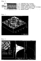
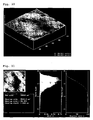
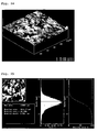
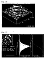
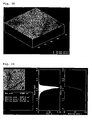
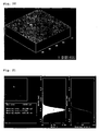
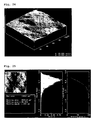
- the surface roughnesses of the molded ferrite sheet and sintered ferrite substrate were determined by measuring the center line average roughness Ra and maximum height Rmax in a region of a square of side 100 ⁇ m using an atomic force microscope AFM (Nano Scope III, manufactured by Digital Instrument).
- the average particle diameter of the ferrite powder was measured by a wet method using Microtrack MT3300 manufactured by Nikkiso Co. Ltd. 5 Gram of the ferrite powder was added to 100 ml of an aqueous solution containing 0.2 % of hexametaphosphoric acid as a dispersant and 0.05 % of a nonionic surfactant (Triton X-100 manufactured by Dow Chemical Company) as a surfactant and the resulting mixture was dispersed for 300 seconds using an ultrasonic homogenizer (Type 300W manufactured by Nikkiso Co. Ltd.). Then, the volumetric distribution was measured under the following conditions; measuring time: 30 seconds, measurement range: from 0.021 to 1408 ⁇ m, solvent refractive index: 1.33, particle refractive index: 2.94 and particle shape: nonspherical.
- the thicknesses of the four corners of a sample piece with an external size of 80 mm x 80 mm cut from the molded sheet were measured with Digimatic Indicator ID-S112 manufactured by Mitsutoyo Corporation and the average of the thicknesses was taken as the thickness of the sheet.
- the sintered density of the sintered ferrite substrate was calculated from its volume obtained from outer dimensions thereof and its weight.
- the sintered ferrite substrate was cut into a test piece having a ring shape with an outer diameter of 14 mm and an inner diameter of 8 mm and its thickness was measured.
- the magnetic permeability of the test piece at a frequency of 13.56 MHz was measured using an Impedance Analyzer HP4291A (manufactured by Hewlett-Packard Development Company) and a jig (HP1645A) attached to the test station thereof or Impedance Analyzer (E4991A manufactured by Agilent Technologies Co., Ltd.) and a jig (16454A) attached to its test station.
- the resonance characteristics of the antenna module were obtained by measuring the resonance characteristics of a conductive loop antenna having a structure as shown in FIG. 1 .
- the frequency characteristics of the impedance of the power supply line for the laminated antenna module configured as shown in FIG. 1 were measured.
- a capacitor was connected in parallel to the power supply line and its capacitance was adjusted.
- the degree of resonance Q was measured using an impedance analyzer HP4291A manufactured by Hewlett-Packard Development Company.
- the resonant frequency and the degree of resonance Q were measured under the same conditions as those set for the case where no iron plate was laminated for comparison.
- the surface electric resistance of the conductive layer was measured by a four probe method (according to JISK 7149) using an electric resistivity meter Loresta-GP (MCP-T600 manufactured by Mitsubishi Chemical Corporation).
- a pressure kneader 1,000 parts by weight of a ferrite powder, obtained by surface-treating 1,000 parts by weight of Ni-Zn-Cu ferrite powder (composition: Fe 2 O 3 : 48.5 mol %, NiO: 20.5 mol %, ZnO: 20.5 mol %, CuO: 10.5 mol %; calcinations conditions: 850°C, 90 minutes; cumulative 50 % volume diameter: adjusted to 0.7 ⁇ m) with 10 parts by weight of a titanate-based coupling agent (KR-TTS manufactured by Ajinomoto Co., Inc.), 50 parts by weight of a thermoplastic elastomer (LUMITAC 22-1 manufactured by Tosoh Corporation), 100 parts by weight of polyethylene having a density of 0.9 g/cm 3 and 20 parts by weight of stearic acid were kneaded at 130°C for 40 minutes.
- a titanate-based coupling agent KR-TTS manufactured by Ajinomoto Co., Inc.
- the thus obtained kneaded mass of a ferrite resin composition was press molded at a temperature of 160°C under a pressure of 9807 kPa (100 kg/cm 2 ) for a pressurization time of 3 minutes using an iron plate, which had been sandblasted to have a center line average roughness of 450 nm and a maximum height of 8 ⁇ m, to obtain a molded ferrite sheet having a thickness of 77 ⁇ m and a size of 100 mm square. Ten such sheets were prepared and stacked one upon another.
- the stacked substrates were placed between top and bottom alumina setters (manufactured by Kikusui Chemical Industries Co., Ltd.) as support plate means and heated at 500°C for 10 hours for removing the organic binder, followed by sintering at 920°C for 2 hours to obtain sintered substrates. After cooling, the sintered substrates were peeled from each other. It was found that the sintered substrate was able to be easily peeled off without causing any damage.
- the sintered substrate had a thickness of 65 ⁇ m and an outer dimension of 80 mm square.
- test piece having an outer diameter of 14 mm and an inner diameter of 8 mm was cut out from the substrate and measured for its magnetic permeability using Impedance Analyzer (HP4291A manufactured by Hewlett-Packard Inc.) and a jig (HP16454A) attached to its test station. It was found that ⁇ r' and ⁇ r" were 98 and 2.2, respectively, at 13.56 MHz. Thus, the obtained sintered ferrite substrates were not stuck to each other and had good magnetic characteristics.
- the above-obtained molded ferrite sheet was found to have a surface roughness such that the center line average roughness was 420 nm, the maximum height was 6.5 ⁇ m and an area occupancy rate of the cross-sectional area, taken along a horizontal plane at a depth of 50 % of the maximum height in a square of side 100 ⁇ m, was 48 %.
- the obtained sintered ferrite substrate was found to have a surface roughness such that the center line average roughness was 400 nm, the maximum height was 5.5 ⁇ m and an area occupancy rate of the cross-sectional area, taken along a horizontal plane at a depth of 50 % of the maximum height in a square of side 100 ⁇ m, was 45 %.
- Example 1 100 parts by weight of the same Ni-Zn-Cu ferrite as used in Example 1, 2 parts by weight of butyl phthalyl butyl glycolate, 12 parts of a polyvinylalcohol resin (ESLEK B BM-1 manufactured by Sekisui Chemical Co., Ltd.) and 60 parts by weight of a mixed solvent composed of 4 parts of n-butanol and 6 parts of toluene were mixed, dissolved or dispersed to obtain a ferrite-dispersed coating liquid.
- ESLEK B BM-1 manufactured by Sekisui Chemical Co., Ltd.
- the ferrite-dispersed coating liquid was defoamed by an oil rotary vacuum pump and uniformly applied with a doctor blade to a PET film (LUMIMAT 50S200 TRES manufactured by Panak Co., Ltd.), one side of which had been sandblasted to have a center line average roughness of 530 nm and a maximum height of 5.6 ⁇ m, to a given thickness.
- the coating was dried with hot wind at 100°C for 30 minutes to obtain a molded ferrite sheet having a thickness of 204 ⁇ m.
- the molded ferrite sheet was cut into squares of side 100 mm. Each of the cut sheets was peeled off from the PET film.
- the sheets were then sintered in the same conditions as those in Example 1 to obtain sintered ferrite substrates.
- the obtained sintered ferrite substrate was evaluated for its physical properties and was found to have a thickness of 160 ⁇ m, an outer dimension of 80 mm square and magnetic permeability with ⁇ r' of 96 and ⁇ r" of 3. Further, the obtained sintered ferrite substrates did not stick to each other and were easily peeled off from each other.
- the above-obtained molded ferrite sheet was found to have a surface roughness such that the center line average roughness was 370 nm, the maximum height was 4.0 ⁇ m and an area occupancy rate of the cross-sectional area, taken along a horizontal plane at a depth of 50 % of the maximum height in a square of side 100 ⁇ m, was 73 %.
- the surface of the above-obtained molded ferrite sheet which had not been brought into contact with the PET film was found to have a center line average roughness of 104 nm, a maximum height of 1.3 ⁇ m and an area occupancy rate of the cross-sectional area, taken along a horizontal plane at a depth of 50 % of the maximum height in a square of side 100 ⁇ m, of 93 %.
- the surface roughness was able to be controlled at will by the PET film used.
- the above-obtained molded ferrite sheet was found to have a surface roughness such that the center line average roughness was 292 nm, the maximum height was 3.5 ⁇ m and an area occupancy rate of the cross-sectional area, taken along a horizontal plane at a depth of 50 % of the maximum height in a square of side 100 ⁇ m, was 12 %.
- a kneaded mass of a ferrite resin composition was prepared in the same manner as that in Example 1 except that a mixture of 300 parts by weight of Ni-Zn-Cu ferrite powder (composition: Fe 2 O 3 : 48.5 mol %, NiO: 20.5 mol %, ZnO: 20.5 mol %, CuO: 10.5 mol %; calcination conditions: 1,000°C, 90 minutes; cumulative 50 % volume diameter: 6 ⁇ m) and 700 parts by weight of the same Ni-Zn-Cu ferrite powder (cumulative 50 % volume diameter: 0.7 ⁇ m) as used in Example 1 was used.
- the thus obtained kneaded mass was press molded at a temperature of 160°C under a pressure of 9807 kPa (100kg/cm 2 ) for a pressurization time of 3 minutes using an iron plate, which had been processed to have a center line average roughness of 120 nm and a maximum roughness of 2 ⁇ m, to obtain a molded ferrite sheet having a thickness of 200 ⁇ m and an outer size of 100 mm.
- sintered ferrite substrates were prepared in the same manner as that in Example 1.
- the obtained sintered ferrite substrate was evaluated for its physical properties and was found to have a thickness of 167 ⁇ m and magnetic permeability with ⁇ r' of 80 and ⁇ r" of 1.1 at 13.56 MHz. Further, the substrates did not stick to each other and were easily peeled off from each other.
- the above-obtained molded ferrite sheet had a center line average roughness of 270 nm, a maximum height of 5.0 ⁇ m and an area occupancy rate of the cross-sectional area, taken along a horizontal plane at a depth of 50 % of the maximum height in a square of side 100 ⁇ m, of 20 %.
- the sintered ferrite substrate had surface roughness such that the center line average roughness was 250 nm, the maximum height was 4.0 ⁇ m and the area occupancy rate of the cross-sectional area, taken along a horizontal plane at a depth of 50 % of the maximum height in a square of side 100 ⁇ m, was 18 %.
- Sintered ferrite substrates were obtained in the same manner as that in Example 2 except that the application of the ferrite-dispersed coating liquid using the doctor blade was carried out under conditions so that a molded ferrite sheet obtained had a thickness of 42 ⁇ m.
- the obtained sintered ferrite substrate was evaluated for its physical properties and was found to have a thickness of 37 ⁇ m and magnetic permeability with ⁇ r' of 95 and ⁇ r" of 2 at 13.56 MHz. Further, the substrates did not stick to each other and were easily peeled off from each other.
- the obtained molded ferrite sheet had surface roughness such that the center line average roughness of 435 nm, the maximum height of 6.3 ⁇ m and the area occupancy rate of the cross-sectional area, taken along a horizontal plane at a depth of 50 % of the maximum height in a square of side 100 ⁇ m, was 52 %.
- the sintered ferrite substrate had surface roughness such that the center line average roughness was 425 nm, the maximum height was 4.9 ⁇ m and the area occupancy rate of the cross-sectional area, taken along a horizontal plane at a depth of 50 % of the maximum height in a square of side 100 ⁇ m, was 50 %.
- Sintered ferrite substrates were obtained in the same manner as that in Example 2 except that the application of the ferrite-dispersed coating liquid using the doctor blade was carried out under conditions so that a molded ferrite sheet obtained had a thickness of 405 ⁇ m.
- the obtained sintered ferrite substrate was evaluated for its physical properties and was found to have a thickness of 350 ⁇ m and magnetic permeability with ⁇ r' of 102 and ⁇ r" of 3.2 at 13.56 MHz. Further, the substrates did not stick to each other and was easily peeled off from each other.
- the obtained molded ferrite sheet had surface roughness such that the center line average roughness of 409 nm, the maximum height of 6.8 ⁇ m and the area occupancy rate of the cross-sectional area, taken along a horizontal plane at a depth of 50 % of the maximum height in a square of side 100 ⁇ m, was 58 %.
- the sintered ferrite substrate had surface roughness such that the center line average roughness was 388 nm, the maximum height was 5.6 ⁇ m and the area occupancy rate of the cross-sectional area, taken along a horizontal plane at a depth of 50 % of the maximum height in a square of side 100 ⁇ m, was 41 %.
- a kneaded mass of a ferrite resin composition was prepared in the same manner as that in Example 1.
- sintered ferrite substrates were prepared in the same manner as that in Example 1 except that an iron plate processed to have a center line average roughness of 120 nm and a maximum roughness of 2 ⁇ m was used in the press molding.
- the substrates stuck so tightly to each other that it was difficult to peel off the substrates from each other. Although the substrate was partly unstuck from each other, breakage occurred when it was forcibly separated therefrom. Thus, no sintered ferrite substrates having a size of 80 mm square were obtained.
- the obtained sintered ferrite substrate had magnetic permeability with ⁇ r' of 98 and ⁇ r" of 1.9 at 13.56 MHz.
- the obtained molded ferrite sheet had surface roughness such that the center line average roughness of 115 nm, the maximum height of 1.8 ⁇ m and the area occupancy rate of the cross-sectional area, taken along a horizontal plane at a depth of 50 % of the maximum height in a square of side 100 ⁇ m, was 2 %.
- the sintered ferrite substrate had surface roughness such that the center line average roughness was 98 nm, the maximum height was 1.1 ⁇ m and the area occupancy rate of the cross-sectional area, taken along a horizontal plane at a depth of 50 % of the maximum height in a square of side 100 ⁇ m, was 2 %.
- a ferrite-dispersed coating liquid was prepared in the same manner as that in Example 2.
- the obtained coating liquid was uniformly applied with a doctor blade to a PET film (not sandblasted) having a center line average roughness of 17 nm, a maximum height of 0.3 ⁇ m and a thickness of 50 ⁇ m. This was dried with hot wind at 100°C for 30 minutes to obtain a molded ferrite sheet having a thickness of 202 ⁇ m.
- the sheet was peeled off from the PET film.
- Ten such sheets were stacked one upon another and heated in the same manner as that in Example 1 to obtain sintered ferrite substrates.
- the obtained substrate was evaluated for its properties and was found to have a thickness of 165 ⁇ m. Since the substrates stuck so tightly to each other it was not possible to peel off the substrates from each other.
- the obtained molded ferrite sheet had surface roughness such that the center line average roughness of 66 nm, the maximum height of 1.3 ⁇ m and the area occupancy rate of the cross-sectional area, taken along a horizontal plane at a depth of 50 % of the maximum height in a square of side 100 ⁇ m, was 90 %.
- the sintered ferrite substrate had surface roughness such that the center line average roughness was 44 nm, the maximum height was 0.9 ⁇ m and the area occupancy rate of the cross-sectional area, taken along a horizontal plane at a depth of 50 % of the maximum height in a square of side 100 ⁇ m, was 1 %.
- a sheet was prepared in the same manner as that in Comparative Example 2 and was peeled off from the PET film. That surface of the molded ferrite sheet which had been in contact with the PET film was applied with 50 mg of zirconia powder having an average particle diameter of 5 ⁇ m by brushing. Thereafter, a calcination treatment was carried out in the same manner as that in Comparative Example 2 to obtain sintered ferrite substrates.
- the evaluation of the sintered ferrite substrate revealed that the substrate had magnetic permeability with ⁇ r' of 96 and ⁇ r" of 1.8 at 13.56 MHz.
- the obtained sintered ferrite substrates had deposits of zirconia powder. During the removal of the zirconia powder deposits using a brush, three of the ten substrates were broken. The application of the powder and the removal of the powder were significantly troublesome. The powder deposits were not able to be completely removed.
- Sintered ferrite substrates were prepared in the same manner as that in Example 1 except that an iron plate processed to have a center line average roughness of 1200 nm and a maximum height of 14 ⁇ m was used in the press molding. The substrates did not stuck to each other and were able to be peeled off from each other.
- the obtained sintered ferrite substrate had magnetic permeability with ⁇ r' of 75 and ⁇ r" of 0.6 at 13.56 MHz and, thus, did not have satisfactory magnetic characteristics. Such deterioration of the magnetic permeability is considered to be attributed to the high surface roughness of the iron plate which resulted in an increase of void spaces in the cross-sections of the sintered ferrite substrate.
- a ferrite-dispersed coating liquid was prepared in the same manner as that in Example 2.
- the obtained coating liquid was uniformly applied with a doctor blade to a PET film (U4-50 manufactured by Teijin DuPont Co., Ltd) which had been processed to have a center line average roughness of 252 nm and a maximum height of 3.3 ⁇ m.
- the coating was dried with hot wind at 100°C for 30 minutes to obtain a molded ferrite sheet having a thickness of 200 ⁇ m.
- the sheet was peeled off from the PET film.
- Ten such sheets were stacked one upon another and heat-treated in the same manner as that in Example 1 to obtain sintered ferrite substrates.
- the obtained substrate was evaluated for its properties and was found to have a thickness of 171 ⁇ m.
- the obtained molded ferrite sheet had surface roughness such that the center line average roughness of 319 nm, the maximum height of 3.3 ⁇ m and the area occupancy rate of the cross-sectional area, taken along a horizontal plane at a depth of 50 % of the maximum height in a square of side 100 ⁇ m, was 95 %.
- the sintered ferrite substrate had surface roughness such that the center line average roughness was 246 nm, the maximum height was 3.3 ⁇ m and the area occupancy rate of the cross-sectional area, taken along a horizontal plane at a depth of 50 % of the maximum height in a square of side 100 ⁇ m, was 96 %.
- a double coated adhesive tape (Product name: 467MP, manufactured by Sumitomo 3M Limited) having a thickness of 50 ⁇ m was adhered onto the surface of the sintered ferrite substrate of Example 1 to which roughness had been imparted, thereby obtaining a laminate composed of a sintered ferrite substrate layer of 63 ⁇ m thick and a adhesive layer of 50 ⁇ m thick.
- the laminate was placed on an urethane foam sheet having a thickness of 10 mm and an expansion ratio of about 10-fold and was then pressed with a rubber roller having an outer dimension of about 50 mm and a width of about 15 cm.
- the rubber roller was displaced in the X and Y directions of the laminate with a roll linear pressure of about 1 kg/cm so that cracks were formed throughout the sintered ferrite substrate.
- a test piece having an outer diameter of 14 mm and an inner diameter of 8 mm was cut out and measured for its magnetic permeability.
- the magnetic permeability was found to have ⁇ r' of 83 and ⁇ r" of 0.8 at 13.56 MHz.
- the similar laminate was wound around an iron rod having an outer diameter of 30 mm.
- a test piece was cut out and measured for its magnetic permeability.
- the magnetic permeability was found to have ⁇ r' of 82.5 and ⁇ r" of 0.8 at 13.56 MHz and was similar to the above.
- the obtained laminates had good bendability and good magnetic permeability ⁇ r' of more than 80.
- a planar antenna composed of a PET film with a thickness of 25 ⁇ m and a 7-turn spiral conductive loop provided on the PET film was prepared.
- the loop had a rectangular shape with a length of 45 mm and a width of 75 mm.
- a molded ferrite sheet having a thickness of 180 ⁇ m was prepared in the same manner as that in Example 2 using the same Ni-Zn-Cu ferrite as used in Example 1. Using a Thomson blade having V-shaped edges of each 30°, V-shaped grooves with a depth of about 90 ⁇ m are formed on one side of the molded sheet. The grooves were arranged at an interval of 2 mm in the form of a grid.
- the obtained molded ferrite sheet having grooves was cut into 100 mm squares and the PET film was peeled off.
- the cut ferrite sheets were calcined in the same manner as that in Example 1 to obtain sintered ferrite substrates each having a thickness of 150 ⁇ m and an outer dimension of 80 mm square.
- a conductive paint (Trade Name: DOTITE XE-9000, manufactured by Fujikura Kasei Co., Ltd.) containing silver and copper powder dispersed in a polyester-based resin was applied to the surface of the substrate which was not formed with the grooves. The applied coating was dried at 50°C for 30 minutes to form a conductive layer having a thickness of 30 ⁇ m and a surface electric resistance of 0.2 ⁇ /square.
- a double coated adhesive tape (Product name: 467MP, manufactured by Sumitomo 3M Limited) was adhered.
- the sintered ferrite substrate layer was divided in the same manner as that in Example 6. The divided pieces were substantially uniform in shape and each in the form of a square of side 2 mm.
- the magnetic permeability of the laminate sheet was found to have ⁇ r' of 84 and ⁇ r" of 0.4.
- an antenna module was prepared by bonding the above-obtained conductive loop antenna and the above-obtained laminate sheet together using a double coated adhesive tape (Product name: 467MP, manufactured by Sumitomo 3M Limited) such that the conductive loop of the antenna faces the opposite surface of the sintered ferrite substrate from the conductive layer.
- the bonding was carried out so that no gaps were formed in each of the bonding surfaces. Since obtained module had a resonant frequency of the antenna module to 10.8 MHz and Q of 68, a capacitor was connected in parallel to the loop antenna to adjust the resonant frequency to a range of 13.5 to 13.6 by changing the capacity. After the adjustment, the Q value was 64.
- the resonant frequency was measured in a state where the conductive layer of the antenna module was in contact with an iron plate having a thickness of 1 mm, no change of the resonant frequency was observed before and after the attachment of the iron plate.
- An antenna module was prepared in the same manner as that in Example 7 except that the conductive layer was formed on the sintered ferrite substrate by applying thereon a nickel-acrylic-based conductive paint (Trade Name: DOTITE FN-101), followed by drying at 50°C for 30 minutes and had a surface electric resistance of 2 ⁇ /square.
- the evaluation of the obtained antenna module revealed that the resonant frequency was 13.6 MHz and the Q value was 60. No change of the resonant frequency was observed before and after the attachment of the iron plate.
- An antenna module was prepared in the same manner as that in Example 7 except that the conductive layer was formed on the sintered ferrite substrate by printing a conductive silver paste on a green sheet of the substrate, followed by sintering the laminate at 900°C and had a thickness of 10 ⁇ m.
- the evaluation of the obtained antenna module revealed that the surface electric resistance of the conductive layer was 0.1 ⁇ /square, the resonant frequency was 13.55 MHz and the Q value was 66. No change of the resonant frequency was observed before and after the attachment of the iron plate.
- An antenna module was prepared in the same manner as that in Example 7 except that a conductive layer was not formed on the sintered ferrite substrate.
- the obtained antenna module without an iron plate laminated thereon had a resonant frequency of 13.55 MHz and a Q value of 67.
- the resonant frequency was measured with an iron plate of 1 mm thick laminated in the same manner as that in Example 7, the resonant frequency was 11.5 MHz and shifted to a low frequency side by 2 MHz, though the Q value was 67 and not changed. Because of the frequency shift, no resonance occurred at 13.56 MHz. The communication strength was considerably low.
- the obtained antenna module had a resonant frequency of 14.1 MHz, when an iron plate was laminated thereon. Thus, the resonant frequency change was smaller as compared with the antenna module of Comparative Example 6. However, the communication strength was reduced.
- the obtained antenna was measured for its resonance characteristics. It was found that the resonant frequency was changed to 10.9 MHz and that the communication strength at 13.56 MHz was reduced.
- a pressure kneader 1,000 parts by weight of a ferrite powder, obtained by surface-treating 1,000 parts by weight of Mg-Zn-Cu ferrite powder (composition: Fe 2 O 3 : 48.5 mol %, MgO: 27.0 mol %, ZnO: 14.5 mol %, CuO: 10.0 mol %; calcination conditions: 850°C, 180 minutes; cumulative 50 % volume diameter: adjusted to 0.7 ⁇ m) with 10 parts by weight of a titanate-based coupling agent (KR-TTS manufactured by Ajinomoto Co., Inc.), 50 parts by weight of a thermoplastic elastomer (LUMITAC 22-1 manufactured by Tosoh Corporation), 100 parts by weight of polyethylene having a density of 0.9 g/cm 3 and 20 parts by weight of stearic acid were kneaded at 130°C for 40 minutes.
- a titanate-based coupling agent KR-TTS manufactured by Ajinomoto Co.,
- the thus obtained kneaded mass of a ferrite resin composition was press molded at a temperature of 160°C under a pressure of 9807 kPa (100 kg/cm 2 ) for a pressurization time of 3 minutes using an iron plate, which had been sandblasted to have a center line average roughness (Ra) of 450 nm and a maximum height (Rmax) of 8 ⁇ m, to obtain a molded ferrite sheet having a thickness of 74 ⁇ m and a size of 100 mm square.
- the obtained sintered substrate had a thickness of 60 ⁇ m and an outer dimension of 80 mm square.
- a test piece having an outer diameter of 14 mm and an inner diameter of 8 mm was cut out from the substrate and measured for its magnetic permeability using Impedance Analyzer (E4991A manufactured by Agilent Technologies Co., Ltd.) and a jig (16454A) attached to its test station. It was found that ⁇ r' and ⁇ r" were 161 and 48, respectively, at 13.56 MHz. Thus, the obtained sintered ferrite substrates were not stuck to each other and had good magnetic characteristics.
- the above-obtained molded ferrite sheet was found to have a surface roughness such that the center line average roughness (Ra) was 380 nm, the maximum height (Rmax) was 4.8 ⁇ m and an area occupancy rate of the cross-sectional area, taken along a horizontal plane at a depth of 50 % of the maximum height in a square of side 100 ⁇ m, was 38 %.
- the obtained sintered ferrite substrate was found to have a surface roughness such that the center line average roughness (Ra) was 366 nm, the maximum height (Rmax) was 4.1 ⁇ m and an area occupancy rate of the cross-sectional area, taken along a horizontal plane at a depth of 50 % of the maximum height in a square of side 100 ⁇ m, was 31 %.
- the ferrite-dispersed coating liquid was defoamed by an oil rotary vacuum pump and uniformly applied with a doctor blade to a PET film (LUMIMAT 50S200 TRES manufactured by Panak Co., Ltd.), one side of which had been sandblasted to have a center line average roughness (Ra) of 530 nm and a maximum height (Rmax) of 5.6 ⁇ m, to a given thickness.
- the coating was dried with hot wind at 100°C for 30 minutes to obtain a molded ferrite sheet having a thickness of 210 ⁇ m.
- the molded ferrite sheet was cut into squares of side 100 mm. Each of the cut sheets was peeled off from the PET film. The sheets were then sintered in the same conditions as those in Example 10 to obtain sintered ferrite substrates.
- the obtained sintered ferrite substrate was evaluated for its physical properties and was found to have a thickness of 174 ⁇ m, an outer dimension of 80 mm square and magnetic permeability with ⁇ r' of 158 and ⁇ r" of 33. Further, the obtained sintered ferrite substrates did not stick to each other and were easily peeled off from each other.
- the above-obtained molded ferrite sheet was found to have a surface roughness such that the center line average roughness (Ra) was 450 nm, the maximum height (Rmax) was 5.1 ⁇ m and an area occupancy rate of the cross-sectional area, taken along a horizontal plane at a depth of 50 % of the maximum height in a square of side 100 ⁇ m, was 40 %.
- the surface of the above-obtained molded ferrite sheet which had not been brought into contact with the PET film was found to have a center line average roughness (Ra) of 131 nm, a maximum height (Rmax) of 1.8 ⁇ m and an area occupancy rate of the cross-sectional area, taken along a horizontal plane at a depth of 50 % of the maximum height in a square of side 100 ⁇ m, of 97 %.
- Ra center line average roughness
- Rmax maximum height
- the above-obtained molded ferrite sheet was found to have a surface roughness such that the center line average roughness (Ra) was 338 nm, the maximum height (Rmax) was 3.6 ⁇ m and an area occupancy rate of the cross-sectional area, taken along a horizontal plane at a depth of 50 % of the maximum height in a square of side 100 ⁇ m, was 21 %.
- a kneaded mass of a ferrite resin composition was prepared in the same manner as that in Example 10 except that a mixture of 300 parts by weight of Mg-Zn-Cu ferrite powder (composition: Fe 2 O 3 : 48.5 mol %, MgO: 27.0 mol %, ZnO: 14.5 mol %, CuO: 10.0 mol %; calcination conditions: 1,000°C, 180 minutes; cumulative 50 % volume diameter: 6 ⁇ m) and 700 parts by weight of the same Mg-Zn-Cu ferrite powder (cumulative 50 % volume diameter: 0.7 ⁇ m) as used in Example 10 was used.
- Mg-Zn-Cu ferrite powder composition: Fe 2 O 3 : 48.5 mol %, MgO: 27.0 mol %, ZnO: 14.5 mol %, CuO: 10.0 mol %
- calcination conditions 1,000°C, 180 minutes
- cumulative 50 % volume diameter: 6 ⁇ m cumulative 50 %
- the thus obtained kneaded mass was press molded at a temperature of 160°C under a pressure of 9807 kPa (100kg/cm 2 ) for a pressurization time of 3 minutes using an iron plate, which had been processed to have a center line average roughness (Ra) of 120 nm and a maximum roughness of 2 ⁇ m, to obtain a molded ferrite sheet having a thickness of 188 ⁇ m and an outer size of 100 mm.
- sintered ferrite substrates were prepared in the same manner as that in Example 10.
- the obtained sintered ferrite substrate was evaluated for its physical properties and was found to have a thickness of 157 ⁇ m and magnetic permeability with ⁇ r' of 144 and ⁇ r" of 21 at 13.56 MHz. Further, the substrates did not stick to each other and were easily peeled off from each other.
- the above-obtained molded ferrite sheet had a center line average roughness (Ra) of 361 nm, a maximum height (Rmax) of 6.2 ⁇ m and an area occupancy rate of the cross-sectional area, taken along a horizontal plane at a depth of 50 % of the maximum height in a square of side 100 ⁇ m, of 67 %.
- the sintered ferrite substrate had surface roughness such that the center line average roughness (Ra) was 305 nm, the maximum height (Rmax) was 4.0 ⁇ m and the area occupancy rate of the cross-sectional area, taken along a horizontal plane at a depth of 50 % of the maximum height in a square of side 100 ⁇ m, was 49 %.
- Sintered ferrite substrates were obtained in the same manner as that in Example 11 except that the application of the ferrite-dispersed coating liquid using the doctor blade was carried out under conditions so that a molded ferrite sheet obtained had a thickness of 43 ⁇ m.
- the obtained sintered ferrite substrate was evaluated for its physical properties and was found to have a thickness of 37 ⁇ m and magnetic permeability with ⁇ r' of 156 and ⁇ r" of 31 at 13.56 MHz. Further, the substrates did not stick to each other and were easily peeled off from each other.
- the obtained molded ferrite sheet had surface roughness such that the center line average roughness (Ra) of 345 nm, the maximum height (Rmax) of 4.0 ⁇ m and the area occupancy rate of the cross-sectional area, taken along a horizontal plane at a depth of 50 % of the maximum height in a square of side 100 ⁇ m, was 23 %.
- the sintered ferrite substrate had surface roughness such that the center line average roughness (Ra) was 289 nm, the maximum height (Rmax) was 3.1 ⁇ m and the area occupancy rate of the cross-sectional area, taken along a horizontal plane at a depth of 50 % of the maximum height in a square of side 100 ⁇ m, was 12 %.
- Sintered ferrite substrates were obtained in the same manner as that in Example 11 except that the application of the ferrite-dispersed coating liquid using the doctor blade was carried out under conditions so that a molded ferrite sheet obtained had a thickness of 377 ⁇ m.
- the obtained sintered ferrite substrate was evaluated for its physical properties and was found to have a thickness of 326 ⁇ m and magnetic permeability with ⁇ r' of 167 and ⁇ r" of 50 at 13.56 MHz. Further, the substrates did not stick to each other and was easily peeled off from each other.
- the obtained molded ferrite sheet had surface roughness such that the center line average roughness (Ra) of 634 nm, the maximum height (Rmax) of 7.8 ⁇ m and the area occupancy rate of the cross-sectional area, taken along a horizontal plane at a depth of 50 % of the maximum height in a square of side 100 ⁇ m, was 66 %.
- the sintered ferrite substrate had surface roughness such that the center line average roughness (Ra) was 593 nm, the maximum height (Rmax) was 7.8 ⁇ m and the area occupancy rate of the cross-sectional area, taken along a horizontal plane at a depth of 50 % of the maximum height in a square of side 100 ⁇ m, was 39 %.
- a kneaded mass of a ferrite resin composition was prepared in the same manner as that in Example 10.
- sintered ferrite substrates were prepared in the same manner as that in Example 10 except that an iron plate processed to have a center line average roughness (Ra) of 120 nm and a maximum roughness of 2 ⁇ m was used in the press molding.
- the substrates stuck so tightly to each other that it was difficult to peel off the substrates from each other. Although the substrate was partly unstuck from each other, breakage occurred when it was forcibly separated therefrom. Thus, no sintered ferrite substrates having a size of 80 mm square were obtained.
- the obtained sintered ferrite substrate had magnetic permeability with ⁇ r' of 160 and ⁇ r" of 48 at 13.56 MHz.
- the obtained molded ferrite sheet had surface roughness such that the center line average roughness (Ra) of 98 nm, the maximum height (Rmax) of 0.9 ⁇ m and the area occupancy rate of the cross-sectional area, taken along a horizontal plane at a depth of 50 % of the maximum height in a square of side 100 ⁇ m, was 5 %.
- the sintered ferrite substrate had surface roughness such that the center line average roughness (Ra) was 81 nm, the maximum height (Rmax) was 0.8 ⁇ m and the area occupancy rate of the cross-sectional area, taken along a horizontal plane at a depth of 50 % of the maximum height in a square of side 100 ⁇ m, was 1 %.
- a ferrite-dispersed coating liquid was prepared in the same manner as that in Example 11.
- the obtained coating liquid was uniformly applied with a doctor blade to a PET film (not sandblasted) having a center line average roughness (Ra) of 17 nm, a maximum height (Rmax) of 0.3 ⁇ m and a thickness of 50 ⁇ m. This was dried with hot wind at 100°C for 30 minutes to obtain a molded ferrite sheet having a thickness of 217 ⁇ m.
- the sheet was peeled off from the PET film. Ten such sheets were stacked one upon another and heated in the same manner as that in Example 10 to obtain sintered ferrite substrates.
- the obtained substrate was evaluated for its properties and was found to have a thickness of 177 ⁇ m. Since the substrates stuck so tightly to each other it was not possible to peel off the substrates from each other.
- the obtained molded ferrite sheet had surface roughness such that the center line average roughness (Ra) of 78 nm, the maximum height (Rmax) of 1.8 ⁇ m and the area occupancy rate of the cross-sectional area, taken along a horizontal plane at a depth of 50 % of the maximum height in a square of side 100 ⁇ m, was 87 %.
- the sintered ferrite substrate had surface roughness such that the center line average roughness (Ra) was 54 nm, the maximum height (Rmax) was 1.3 ⁇ m and the area occupancy rate of the cross-sectional area, taken along a horizontal plane at a depth of 50 % of the maximum height in a square of side 100 ⁇ m, was 0.2 %.
- a sheet was prepared in the same manner as that in Comparative Example 10 and was peeled off from the PET film. That surface of the molded ferrite sheet which had been in contact with the PET film was applied with 50 mg of zirconia powder having an average particle diameter of 5 ⁇ m by brushing. Thereafter, a calcination treatment was carried out in the same manner as that in Comparative Example 10 to obtain sintered ferrite substrates.
- the evaluation of the sintered ferrite substrate revealed that the substrate had magnetic permeability with ⁇ r' of 157 and ⁇ r" of 31 at 13.56 MHz.
- the obtained sintered ferrite substrates had deposits of zirconia powder. During the removal of the zirconia powder deposits using a brush, four of the ten substrates were broken. The application of the powder and the removal of the powder were significantly troublesome. The powder deposits were not able to be completely removed.
- Sintered ferrite substrates were prepared in the same manner as that in Example 10 except that an iron plate processed to have a center line average roughness (Ra) of 1200 nm and a maximum height (Rmax) of 14 ⁇ m was used in the press molding. The substrates did not stuck to each other and were able to be peeled off from each other.
- the obtained sintered ferrite substrate had magnetic permeability with ⁇ r' of 78 and ⁇ r" of 1 at 13.56 MHz and, thus, did not have satisfactory magnetic characteristics. Such deterioration of the magnetic permeability is considered to be attributed to the high surface roughness of the iron plate which resulted in an increase of void spaces in the cross-sections of the sintered ferrite substrate.
- a ferrite-dispersed coating liquid was prepared in the same manner as that in Example 11.
- the obtained coating liquid was uniformly applied with a doctor blade to a PET film (U4-50 manufactured by Teijin DuPont Co., Ltd) which had been processed to have a center line average roughness (Ra) of 252 nm and a maximum height (Rmax) of 3.3 ⁇ m.
- the coating was dried with hot wind at 100°C for 30 minutes to obtain a molded ferrite sheet having a thickness of 198 ⁇ m.
- the sheet was peeled off from the PET film. Ten such sheets were stacked one upon another and heat-treated in the same manner as that in Example 10 to obtain sintered ferrite substrates.
- the obtained substrate was evaluated for its properties and was found to have a thickness of 169 ⁇ m. Since the substrates stuck so tightly to each other it was not possible to peel off the substrates from each other.
- the obtained molded ferrite sheet had surface roughness such that the center line average roughness (Ra) of 246 nm, the maximum height (Rmax) of 2.6 ⁇ m and the area occupancy rate of the cross-sectional area, taken along a horizontal plane at a depth of 50 % of the maximum height in a square of side 100 ⁇ m, was 97 %.
- the sintered ferrite substrate had surface roughness such that the center line average roughness (Ra) was 201 nm, the maximum height (Rmax) was 2.1 ⁇ m and the area occupancy rate of the cross-sectional area, taken along a horizontal plane at a depth of 50 % of the maximum height in a square of side 100 ⁇ m, was 96 %.
- a double coated adhesive tape (Product name: 467MP, manufactured by Sumitomo 3M Limited) having a thickness of 50 ⁇ m was adhered onto the surface of the sintered ferrite substrate of Example 10 to which roughness had been imparted, thereby obtaining a laminate composed of a sintered ferrite substrate layer of 60 ⁇ m thick and a adhesive layer of 50 ⁇ m thick.
- the laminate was placed on an urethane foam sheet having a thickness of 10 mm and an expansion ratio of about 10-fold and was then pressed with a rubber roller having an outer dimension of about 50 mm and a width of about 15 cm.
- the rubber roller was displaced in the X and Y directions of the laminate with a roll linear pressure of about 1 kg/cm so that cracks were formed throughout the sintered ferrite substrate.
- a test piece having an outer diameter of 14 mm and an inner diameter of 8 mm was cut out and measured for its magnetic permeability.
- the magnetic permeability was found to have ⁇ r' of 121 and ⁇ r" of 10 at 13.56 MHz.
- the similar laminate was wound around an iron rod having an outer diameter of 30 mm.
- a test piece was cut out and measured for its magnetic permeability.
- the magnetic permeability was found to have ⁇ r' of 120 and ⁇ r" of 10 at 13.56 MHz and was similar to the above.
- the obtained laminates had good bendability and good magnetic permeability ⁇ r' of more than 80.
- a planar antenna composed of a PET film with a thickness of 25 ⁇ m and a 7-turn spiral conductive loop provided on the PET film was prepared.
- the loop had a rectangular shape with a length of 45 mm and a width of 75 mm.
- a molded ferrite sheet having a thickness of 185 ⁇ m was prepared in the same manner as that in Example 11 using the same Mg-Zn-Cu ferrite as used in Example 10. Using a Thomson blade having V-shaped edges of each 30°, V-shaped grooves with a depth of about 90 ⁇ m are formed on one side of the molded sheet. The grooves were arranged at an interval of 2 mm in the form of a grid. The obtained molded ferrite sheet having grooves was cut into 100 mm squares and the PET film was peeled off. The cut ferrite sheets were calcined in the same manner as that in Example 10 to obtain sintered ferrite substrates.
- the obtained sintered ferrite substrate had a thickness of 143 ⁇ m and an outer dimension of 80 mm square.
- a conductive paint (Trade Name: DOTITE XE-9000, manufactured by Fujikura Kasei Co., Ltd.) containing silver and copper powder dispersed in a polyester-based resin was applied to the surface of the substrate which was not formed with the grooves. The applied coating was dried at 50°C for 30 minutes to form a conductive layer having a thickness of 30 ⁇ m and a surface electric resistance of 0.2 ⁇ /square.
- a double coated adhesive tape (Product name: 467MP, manufactured by Sumitomo 3M Limited) was adhered.
- the sintered ferrite substrate layer was divided in the same manner as that in Example 15. The divided pieces were substantially uniform in shape and each in the form of a square of side 2 mm.
- the magnetic permeability of the laminate sheet was found to have ⁇ r' of 119 and ⁇ r" of 9.0.
- an antenna module was prepared by bonding the above-obtained conductive loop antenna and the above-obtained laminate sheet together using a double coated adhesive tape (Product name: 467MP, manufactured by Sumitomo 3M Limited) such that the conductive loop of the antenna faces the opposite surface of the sintered ferrite substrate from the conductive layer.
- the bonding was carried out so that no gaps were formed in each of the bonding surfaces. Since obtained module had a resonant frequency of the antenna module to 15.5 MHz and Q of 67, a capacitor was connected in parallel to the loop antenna to adjust the resonant frequency to a range of 13.5 to 13.6 by changing the capacity. No change of Q was seen after the adjustment.
- the resonant frequency was measured in a state where the conductive layer of the antenna module was in contact with an iron plate having a thickness of 1 mm, no change of the resonant frequency was observed before and after the attachment of the iron plate.
- An antenna module was prepared in the same manner as that in Example 16 except that the conductive layer was formed on the sintered ferrite substrate by applying thereon a nickel-acrylic-based conductive paint (Trade Name: DOTITE FN-101), followed by drying at 50°C for 30 minutes and had a surface electric resistance of 2 ⁇ /square.
- the evaluation of the obtained antenna module revealed that the resonant frequency was 13.6 MHz and the Q value was 63. No change of the resonant frequency was observed before and after the attachment of the iron plate.
- An antenna module was prepared in the same manner as that in Example 16 except that the conductive layer was formed on the sintered ferrite substrate by printing a conductive silver paste on a green sheet of the substrate, followed by sintering the laminate at 900°C and had a thickness of 10 ⁇ m.
- the evaluation of the obtained antenna module revealed that the surface electric resistance of the conductive layer was 0.1 Q/square, the resonant frequency was 13.55 MHz and the Q value was 63. No change of the resonant frequency was observed before and after the attachment of the iron plate.
- An antenna module was prepared in the same manner as that in Example 16 except that a conductive layer was not formed on the sintered ferrite substrate.
- the obtained antenna module without an iron plate laminated thereon had a resonant frequency of 13.5 MHz and a Q value of 66.
- the resonant frequency was measured with an iron plate of 1 mm thick laminated in the same manner as that in Example 13, the resonant frequency was 15.8 MHz and shifted to a high frequency side by 2.3 MHz, though the Q value was 66 and not changed. Because of the frequency shift, no resonance occurred at 13.56 MHz. The communication strength was considerably low.
- the obtained antenna module had a resonant frequency of 13.9 MHz, when an iron plate was laminated thereon. Thus, the resonant frequency change was smaller as compared with the antenna module of Comparative Example 14. However, the communication strength was reduced.
- the obtained antenna was measured for its resonance characteristics. It was found that the resonant frequency was changed to 15.0 MHz and that the communication strength at 13.56 MHz was reduced.
Claims (12)
- Feuille de ferrite moulée possédant des surfaces opposées et une épaisseur située dans la plage allant de 30 µm à 430 µm, au moins une surface desdites surfaces opposées présentant les caractéristiques (a) à (c) suivantes de rugosité de surface :(a) une rugosité moyenne arithmétique située dans la plage allant de 170 nm à 800 nm,(b) une hauteur maximale située dans la plage allant de 3 µm à 10 µm, et(c) un taux d'occupation de surface d'une section prise le long d'un plan horizontal à une profondeur de 50 % de la hauteur maximale dans un carré de 100 µm de côté situé dans la plage allant de 10 % à 80 %.
- Feuille de ferrite moulée selon la revendication 1, dans laquelle ladite au moins une surface a été rendue rugueuse par sablage.
- Feuille de ferrite moulée selon la revendication 1, qui a été préparée par :(a) moulage sous pression au moyen d'un moule ou d'un cylindre de calandre possédant une surface rugueuse, de sorte que la rugosité de la surface rugueuse dudit moule ou cylindre de calandre est transférée sur une surface de ladite feuille de ferrite moulée en contact avec la surface rugueuse dudit moule ou cylindre de calandre ; ou(b) application d'un revêtement composé d'un liquide de revêtement contenant de la ferrite dispersée sur une surface d'un film plastique qui a été rendu rugueux par sablage et séchage du revêtement appliqué, de sorte que la rugosité dudit film plastique est transférée à une surface du revêtement sec en contact avec la surface rugueuse dudit film plastique ; ou(c) application d'un revêtement composé d'un liquide de revêtement contenant de la ferrite dispersée sur un support et séchage du revêtement appliqué, dans laquelle la ferrite a été obtenue par l'ajustement d'une taille de particule d'une poudre de ferrite possédant un diamètre moyen de particule de 0,1 µm à 10 µm, de sorte que lesdites caractéristiques de rugosité de surface sont conférées à une surface du revêtement sec en contact avec ledit support.
- Feuille de ferrite moulée selon l'une quelconque des revendications précédentes, dans laquelle la ferrite est une ferrite spinelle à base de Ni-Zn-Cu ou une ferrite spinelle à base de Mg-Zn-Cu.
- Substrat de ferrite frittée possédant des surfaces opposées et une épaisseur située dans la plage allant de 25 µm à 360 µm, au moins une surface desdites surfaces opposées présentant les caractéristiques (a) à (c) suivantes de rugosité de surface :(a) une rugosité moyenne arithmétique située dans la plage allant de 150 nm à 700 nm,(b) une hauteur maximale située dans la plage allant de 2 µm à 9 µm, et(c) un taux d'occupation de surface d'une section prise le long d'un plan horizontal à une profondeur de 50 % de la hauteur maximale dans un carré de 100 µm de côté situé dans la plage allant de 10 % à 80 %,dans lequel ledit substrat de ferrite frittée peut être obtenu par le traitement thermique d'une feuille de ferrite moulée selon l'une quelconque des revendications 1 à 4.
- Substrat de ferrite frittée selon la revendication 5, dans lequel la ferrite est :(a) une ferrite spinelle à base de Ni-Zn-Cu et présente une perméabilité magnétique avec une partie réelle µr' et une partie imaginaire µr" qui, respectivement, n'est pas inférieure à 80 et n'est pas supérieure à 20 à 13,56 MHz ; ou(b) une ferrite spinelle à base de Mg-Zn-Cu et présente une perméabilité magnétique avec une partie réelle µr' et une partie imaginaire µr" qui, respectivement, n'est pas inférieure à 80 et n'est pas supérieure à 100 à 13,56 MHz.
- Substrat de ferrite frittée selon la revendication 5 ou 6, qui comporte une couche conductrice sur une des surfaces opposées.
- Substrat de ferrite frittée selon l'une quelconque des revendications 5 à 7, qui présente des rainures sur au moins une des surfaces opposées.
- Substrat de ferrite frittée selon l'une quelconque des revendications 5 à 8, qui comporte un film adhésif collé sur au moins une des surfaces opposées et qui est divisé en une pluralité de parties.
- Module d'antenne utilisable dans un support de radiocommunication et dispositif de traitement de support de radiocommunication, comprenant un élément magnétique, une antenne à boucle conductrice située sur un côté dudit élément magnétique et une couche conductrice située sur le côté opposé dudit élément magnétique à partir de l'antenne à boucle conductrice, ledit élément magnétique étant un substrat de ferrite frittée tel que défini dans l'une quelconque des revendications 5 à 9.
- Module d'antenne selon la revendication 10, dans lequel ladite couche conductrice possède une épaisseur qui n'est pas supérieure à 50 µm et une résistance électrique superficielle qui n'est pas supérieure à 3 Ω/carré.
- Module d'antenne selon la revendication 10 ou 11, dans lequel ledit élément magnétique est :(a) un substrat de ferrite spinelle frittée à base de Ni-Zn-Cu ou de Mg-Zn-Cu sur lequel un revêtement composé d'une peinture conductrice à base de résine acrylique ou à base de résine époxy a été appliqué pour former ladite couche conductrice ; ou(b) un substrat de ferrite spinelle frittée à base de Mg-Zn-Cu ou de Ni-Zn-Cu, dans lequel ledit substrat de ferrite frittée et ladite couche conductrice appliquée dessus ont été formés par la formation d'une impression d'une pâte d'argent sur une feuille de ferrite moulée, puis par le frittage et l'intégration ensemble de ladite impression de peinture d'argent et de ladite feuille de ferrite moulée.
Priority Applications (1)
| Application Number | Priority Date | Filing Date | Title |
|---|---|---|---|
| EP14160562.6A EP2747099B1 (fr) | 2007-03-07 | 2008-03-06 | Substrat de ferrite fritté et module d'antenne |
Applications Claiming Priority (2)
| Application Number | Priority Date | Filing Date | Title |
|---|---|---|---|
| JP2007057892 | 2007-03-07 | ||
| JP2007282576A JP5194717B2 (ja) | 2007-10-31 | 2007-10-31 | フェライト成形シート、焼結フェライト基板およびアンテナモジュール |
Related Child Applications (2)
| Application Number | Title | Priority Date | Filing Date |
|---|---|---|---|
| EP14160562.6A Division EP2747099B1 (fr) | 2007-03-07 | 2008-03-06 | Substrat de ferrite fritté et module d'antenne |
| EP14160562.6A Division-Into EP2747099B1 (fr) | 2007-03-07 | 2008-03-06 | Substrat de ferrite fritté et module d'antenne |
Publications (3)
| Publication Number | Publication Date |
|---|---|
| EP1968079A2 EP1968079A2 (fr) | 2008-09-10 |
| EP1968079A3 EP1968079A3 (fr) | 2010-11-03 |
| EP1968079B1 true EP1968079B1 (fr) | 2014-05-14 |
Family
ID=39493918
Family Applications (2)
| Application Number | Title | Priority Date | Filing Date |
|---|---|---|---|
| EP14160562.6A Active EP2747099B1 (fr) | 2007-03-07 | 2008-03-06 | Substrat de ferrite fritté et module d'antenne |
| EP20080250768 Active EP1968079B1 (fr) | 2007-03-07 | 2008-03-06 | Feuille de ferrite moulée, substrat de ferrite fritté et module d'antenne |
Family Applications Before (1)
| Application Number | Title | Priority Date | Filing Date |
|---|---|---|---|
| EP14160562.6A Active EP2747099B1 (fr) | 2007-03-07 | 2008-03-06 | Substrat de ferrite fritté et module d'antenne |
Country Status (5)
| Country | Link |
|---|---|
| US (3) | US7910214B2 (fr) |
| EP (2) | EP2747099B1 (fr) |
| KR (2) | KR101187172B1 (fr) |
| CN (2) | CN103496960B (fr) |
| TW (1) | TWI430295B (fr) |
Families Citing this family (59)
| Publication number | Priority date | Publication date | Assignee | Title |
|---|---|---|---|---|
| KR101187172B1 (ko) * | 2007-03-07 | 2012-09-28 | 도다 고교 가부시끼가이샤 | 페라이트 성형 시트, 소결 페라이트 기판 및 안테나 모듈 |
| US8154456B2 (en) | 2008-05-22 | 2012-04-10 | Philtech Inc. | RF powder-containing base |
| US8188924B2 (en) * | 2008-05-22 | 2012-05-29 | Philtech Inc. | RF powder and method for manufacturing the same |
| KR101620307B1 (ko) | 2009-07-28 | 2016-05-13 | 삼성전자주식회사 | Y-타입의 육방정 페라이트, 그를 이용한 안테나 장치 및 그의 제조 방법 |
| JP5685827B2 (ja) * | 2010-03-29 | 2015-03-18 | ソニー株式会社 | 磁性シート、アンテナモジュール及び電子機器 |
| US8986568B2 (en) * | 2010-03-31 | 2015-03-24 | Tdk Corporation | Sintered magnet and method for producing the sintered magnet |
| JP5606824B2 (ja) * | 2010-08-18 | 2014-10-15 | 株式会社不二製作所 | 金型の表面処理方法及び前記方法で表面処理された金型 |
| KR101286167B1 (ko) * | 2010-11-17 | 2013-07-15 | 주식회사 이엠따블유 | 페라이트 시트 복합체 및 그 제조 방법 |
| CN102437414A (zh) * | 2011-08-04 | 2012-05-02 | 瑞声声学科技(深圳)有限公司 | 射频识别天线的制作方法 |
| CN102263327A (zh) * | 2011-08-04 | 2011-11-30 | 瑞声声学科技(深圳)有限公司 | 射频识别天线的制作方法 |
| CN102427158A (zh) * | 2011-08-11 | 2012-04-25 | 瑞声声学科技(深圳)有限公司 | 射频识别天线的制作方法 |
| MY166125A (en) * | 2011-09-14 | 2018-05-24 | Microconnections Sas | Rfid antenna |
| US9627117B2 (en) * | 2011-10-27 | 2017-04-18 | Arizona Board Of Regents, A Body Corporate Of The State Of Arizona Acting For And On Behalf Of Arizona State University | Thin film ferrite lamination |
| KR101317896B1 (ko) * | 2012-05-07 | 2013-10-16 | 에이큐 주식회사 | 안테나의 흡수체 및 그 제조방법 |
| FR2992313B1 (fr) * | 2012-06-21 | 2014-11-07 | Eurokera | Article vitroceramique et procede de fabrication |
| KR101823542B1 (ko) * | 2012-10-04 | 2018-01-30 | 엘지이노텍 주식회사 | 무선충전용 전자기 부스터 및 그 제조방법 |
| US9824802B2 (en) | 2012-10-31 | 2017-11-21 | Toda Kogyo Corp. | Ferrite sintered plate and ferrite sintered sheet |
| WO2014085659A1 (fr) | 2012-11-28 | 2014-06-05 | The Board Of Trustees Of The University Of Alabama For And On Behalf Of The University Of Alabama | Antennes magnétiques à double polarisation |
| KR101476044B1 (ko) * | 2012-12-06 | 2014-12-23 | 쓰리엠 이노베이티브 프로퍼티즈 캄파니 | 페라이트 그린 시트, 소결 페라이트 시트, 이를 포함하는 페라이트 복합시트 및 도전 루프 안테나 모듈 |
| WO2014088954A1 (fr) * | 2012-12-06 | 2014-06-12 | 3M Innovative Properties Company | Feuille crue en ferrite, feuille en ferrite frittée, feuille composite en ferrite les comprenant, et module à antenne cadre conductrice |
| KR101410306B1 (ko) * | 2012-12-12 | 2014-06-24 | 주식회사 아모텍 | 표면 요철을 가지는 페라이트 시트, 페라이트 시트의 제조 방법 및 페라이트 시트의 표면 처리 장치 |
| WO2014134054A1 (fr) * | 2013-02-26 | 2014-09-04 | The Board Of Trustees Of The University Of Alabama For And On Behalf Of The University Of Alabama | Modules d'antenne comportant des substrats en ferrite |
| JP5585740B1 (ja) | 2013-03-18 | 2014-09-10 | 株式会社村田製作所 | 積層型インダクタ素子および通信装置 |
| US10505269B2 (en) * | 2013-04-28 | 2019-12-10 | The Board Of Trustees Of The University Of Alabama For And On Behalf Of The University Of Alabama | Magnetic antenna structures |
| KR101488897B1 (ko) * | 2013-05-08 | 2015-02-06 | 플라텔코퍼레이션(주) | 방열기능이 부가된 nfc 복합 안테나 및 이의 제조방법 |
| KR20150010519A (ko) | 2013-07-19 | 2015-01-28 | 삼성전자주식회사 | 연자성 자기교환결합 복합 구조체 및 이를 포함한 고주파소자 부품, 안테나 모듈 및 자기저항소자 |
| CN103553585B (zh) * | 2013-10-22 | 2016-04-27 | 瑞声声学科技(深圳)有限公司 | 铁氧体陶瓷的制备方法 |
| EP3064481B1 (fr) * | 2013-10-31 | 2018-09-05 | Toda Kogyo Corp. | Corps en ferrite fritté, plaque en ferrite frittée, et feuille en ferrite frittée |
| WO2015195523A2 (fr) * | 2014-06-17 | 2015-12-23 | A.K. Stamping Company, Inc. | Procédé de réglage précis d'une antenne de communication en champ proche |
| US9923273B2 (en) | 2013-12-02 | 2018-03-20 | A.K. Stamping Company, Inc. | System for manufacturing and tuning an NFC antenna |
| USD755163S1 (en) | 2014-03-13 | 2016-05-03 | Murata Manufacturing Co., Ltd. | Antenna |
| CN105098365B (zh) * | 2014-05-14 | 2018-08-10 | 3M创新有限公司 | 近场通信模块 |
| WO2015178450A1 (fr) * | 2014-05-22 | 2015-11-26 | 戸田工業株式会社 | Plaque de ferrite frittée et feuille de ferrite frittée |
| DE102014210013A1 (de) * | 2014-05-26 | 2015-11-26 | Schaeffler Technologies AG & Co. KG | Magnetische Platine und Verfahren zu deren Herstellung |
| CN104210015B (zh) * | 2014-07-07 | 2016-08-24 | 东莞市美厚塑磁有限公司 | 粘结永磁铁氧体磁胶片的连轧工艺及生产线 |
| KR102384341B1 (ko) * | 2014-12-12 | 2022-04-08 | 미래나노텍(주) | 페라이트 소결체, 이를 포함하는 페라이트 복합 시트 그리고 그 제조 방법 및 이를 위한 패턴 성형 몰드 |
| KR101656822B1 (ko) * | 2015-03-09 | 2016-09-12 | 에스케이씨 주식회사 | 세라믹 시트 제조용 압출 성형 장치, 세라믹 시트, 및 이의 제조방법 |
| CN107836140B (zh) * | 2015-07-14 | 2019-12-06 | 户田工业株式会社 | 铁氧体叠层体和噪声抑制片 |
| CN108141994B (zh) * | 2015-09-30 | 2020-02-07 | 阿莫善斯有限公司 | 磁场屏蔽单元、包括其的模块及包括其的便携式设备 |
| CN105206413A (zh) * | 2015-10-14 | 2015-12-30 | 无锡斯贝尔磁性材料有限公司 | 一种高效柔性磁片加工工艺 |
| KR101619808B1 (ko) * | 2015-10-15 | 2016-05-11 | 주식회사 이엠따블유 | 페라이트 시트, 이의 제조 방법, 및 이를 포함하는 복합 안테나 모듈 |
| KR101657032B1 (ko) * | 2016-03-17 | 2016-09-12 | 정윤화 | 페라이트 적층 시트 |
| US11431100B2 (en) * | 2016-03-25 | 2022-08-30 | Commscope Technologies Llc | Antennas having lenses formed of lightweight dielectric materials and related dielectric materials |
| WO2017165342A1 (fr) | 2016-03-25 | 2017-09-28 | Commscope Technologies Llc | Antennes comportant des lentilles formées de matériaux diélectriques légers, et matériaux diélectriques correspondants |
| JP6399363B2 (ja) * | 2016-05-02 | 2018-10-03 | パウダーテック株式会社 | フェライト粉末、樹脂組成物、電磁波シールド材、電子回路基板、電子回路部品及び電子機器筐体 |
| CN106182374B (zh) * | 2016-07-18 | 2019-04-09 | 上海华源磁业股份有限公司 | 一种薄型铁氧体片的制备工艺 |
| KR20190085941A (ko) * | 2016-11-29 | 2019-07-19 | 파나소닉 아이피 매니지먼트 가부시키가이샤 | 복합 코일 모듈 및 자성 시트 |
| KR101949396B1 (ko) * | 2017-07-10 | 2019-02-19 | 에스케이씨 주식회사 | 매립된 패턴을 갖는 안테나 소자 및 이의 제조방법 |
| KR101964916B1 (ko) * | 2017-08-22 | 2019-04-02 | 에스케이씨 주식회사 | 도전 자성 복합 시트, 안테나 소자 및 이의 제조방법 |
| WO2019055134A1 (fr) | 2017-09-15 | 2019-03-21 | Commscope Technologies Llc | Procédés de préparation d'un matériau diélectrique composite |
| CN108235675A (zh) * | 2018-02-02 | 2018-06-29 | 上海量子绘景电子股份有限公司 | 一种电磁屏蔽片的生产设备 |
| EP3598571B1 (fr) * | 2018-07-17 | 2021-10-06 | LS Mtron Ltd. | Module d'antenne et?son procédé de fabrication |
| KR101968047B1 (ko) * | 2018-07-20 | 2019-04-10 | 엘에스엠트론 주식회사 | 안테나 모듈의 제조방법 |
| KR101968045B1 (ko) * | 2018-07-17 | 2019-04-10 | 엘에스엠트론 주식회사 | 안테나 모듈 |
| US11765839B2 (en) * | 2018-10-10 | 2023-09-19 | Schlumberger Technology Corporation | Additive manufactured 3D electronic substrate |
| CN113168947A (zh) * | 2018-12-20 | 2021-07-23 | 3M创新有限公司 | 磁膜 |
| US11050144B1 (en) * | 2020-05-08 | 2021-06-29 | W. L. Gore & Associates, Inc. | Assembly with at least one antenna and a thermal insulation component |
| CN112768218B (zh) * | 2020-12-22 | 2022-10-21 | 信维通信(江苏)有限公司 | 低损耗隔磁片及其制备方法 |
| US11770906B2 (en) | 2021-08-27 | 2023-09-26 | Schlumberger Technology Corporation | 3D-printed ceramics with conductor infusion for ultra-high-speed electronics |
Family Cites Families (33)
| Publication number | Priority date | Publication date | Assignee | Title |
|---|---|---|---|---|
| JPS5599843A (en) | 1979-01-25 | 1980-07-30 | Tdk Corp | Reception unit |
| JPS612510A (ja) | 1984-06-15 | 1986-01-08 | 松下電工株式会社 | セラミツクス粗面基板の製法 |
| CN1007847B (zh) * | 1984-12-24 | 1990-05-02 | 住友特殊金属株式会社 | 制造具有改进耐蚀性磁铁的方法 |
| JPH0661740B2 (ja) * | 1988-02-16 | 1994-08-17 | 株式会社住友金属セラミックス | セラミックグリーンシート積層体の製造方法 |
| JPH02305416A (ja) | 1989-05-19 | 1990-12-19 | Hitachi Ferrite Ltd | フェライトシート |
| JPH05279044A (ja) | 1992-03-30 | 1993-10-26 | Nisshin Steel Co Ltd | 噴霧焙焼法によるフェライト粉末の製造方法 |
| US6759137B1 (en) * | 1998-08-28 | 2004-07-06 | Centre National De La Recherche Scientifique, Inc. | Opto-magnetic recording medium with a garnet ferrite recording layer, and opto-magnetic information recording/reproducing device |
| JP2000077224A (ja) | 1998-09-02 | 2000-03-14 | Kawasaki Steel Corp | Mn−Znフェライトの製造方法 |
| JP3675264B2 (ja) * | 1999-12-03 | 2005-07-27 | 株式会社村田製作所 | セラミックスラリー、セラミックグリーンシート及び積層セラミック電子部品の製造方法 |
| US6533956B2 (en) * | 1999-12-16 | 2003-03-18 | Tdk Corporation | Powder for magnetic ferrite, magnetic ferrite, multilayer ferrite components and production method thereof |
| US6821618B2 (en) * | 2000-12-22 | 2004-11-23 | Toda Kogyo Corporation | Magnetic recording medium and process for producing the same |
| JP4330850B2 (ja) | 2002-07-12 | 2009-09-16 | 太陽誘電株式会社 | 薄型コイル部品の製造方法,薄型コイル部品及びそれを使用した回路装置 |
| CN1221987C (zh) * | 2002-11-27 | 2005-10-05 | 横店集团东磁股份有限公司 | 高频细晶粒软磁铁氧体磁体材料及其生产工艺 |
| US7625633B2 (en) * | 2003-03-25 | 2009-12-01 | Shin-Etsu Polymer., Ltd. | Electromagnetic noise suppressor, article with electromagnetic noise suppressing function, and their manufacturing methods |
| JP4152856B2 (ja) | 2003-03-25 | 2008-09-17 | 信越ポリマー株式会社 | 電磁波吸収体及び電磁波ノイズ制御電子機器 |
| JP2005019718A (ja) | 2003-06-26 | 2005-01-20 | Koa Corp | セラミック積層部品の製造方法 |
| JP2005015281A (ja) * | 2003-06-26 | 2005-01-20 | Tdk Corp | 焼結部材の製造方法、成形用組成物、フェライトコアの製造方法及びフェライトコア |
| JP4277596B2 (ja) | 2003-06-27 | 2009-06-10 | 戸田工業株式会社 | 焼結フェライト基板 |
| JP2005101111A (ja) | 2003-09-22 | 2005-04-14 | Kyocera Corp | 高周波回路用デバイス基板およびこれに用いる電磁波吸収体 |
| JP4619026B2 (ja) | 2003-10-24 | 2011-01-26 | 京セラ株式会社 | ガラスセラミック基板およびその製造方法 |
| JP2005268463A (ja) | 2004-03-18 | 2005-09-29 | Murata Mfg Co Ltd | 電波吸収体の製造方法 |
| JP2005340759A (ja) | 2004-04-27 | 2005-12-08 | Sony Corp | アンテナモジュール用磁芯部材、アンテナモジュールおよびこれを備えた携帯情報端末 |
| US7924235B2 (en) * | 2004-07-28 | 2011-04-12 | Panasonic Corporation | Antenna apparatus employing a ceramic member mounted on a flexible sheet |
| JP4587758B2 (ja) * | 2004-09-22 | 2010-11-24 | 京セラ株式会社 | ガラスセラミック基板 |
| EP1815558B1 (fr) * | 2004-09-29 | 2014-08-20 | Panasonic Corporation | Feuille magnetique, appareil d'antenne l'utilisant et procede de production d'une feuille magnetique |
| JP4218635B2 (ja) | 2004-12-17 | 2009-02-04 | パナソニック株式会社 | 磁性材の製造方法およびアンテナ装置 |
| EP1879254A4 (fr) | 2005-03-25 | 2010-01-27 | Toray Industries | Antenne plane et procede de fabrication correspondant |
| JP4631536B2 (ja) | 2005-05-23 | 2011-02-16 | 日立金属株式会社 | アンテナ |
| JP3728320B1 (ja) | 2005-06-21 | 2005-12-21 | ニッタ株式会社 | タグ用磁気シールドシートおよびタグ |
| EP1901394B1 (fr) * | 2005-07-07 | 2016-08-31 | Toda Kogyo Corporation | Antenne magnétique |
| JP2007123866A (ja) | 2005-09-30 | 2007-05-17 | Tdk Corp | 薄膜デバイスおよび薄膜インダクタ |
| JP4529906B2 (ja) | 2006-01-10 | 2010-08-25 | Tdk株式会社 | フェライト部品 |
| KR101187172B1 (ko) * | 2007-03-07 | 2012-09-28 | 도다 고교 가부시끼가이샤 | 페라이트 성형 시트, 소결 페라이트 기판 및 안테나 모듈 |
-
2008
- 2008-03-04 KR KR1020080019984A patent/KR101187172B1/ko active IP Right Grant
- 2008-03-05 CN CN201310409292.XA patent/CN103496960B/zh active Active
- 2008-03-05 CN CN201610182890.1A patent/CN105869820B/zh active Active
- 2008-03-06 US US12/073,565 patent/US7910214B2/en active Active
- 2008-03-06 EP EP14160562.6A patent/EP2747099B1/fr active Active
- 2008-03-06 EP EP20080250768 patent/EP1968079B1/fr active Active
- 2008-03-07 TW TW97108120A patent/TWI430295B/zh active
-
2011
- 2011-02-03 US US12/929,603 patent/US20110129641A1/en not_active Abandoned
- 2011-10-17 KR KR1020110105858A patent/KR101359872B1/ko active IP Right Grant
-
2012
- 2012-05-29 US US13/482,100 patent/US9394204B2/en active Active
Also Published As
| Publication number | Publication date |
|---|---|
| EP2747099A2 (fr) | 2014-06-25 |
| US7910214B2 (en) | 2011-03-22 |
| CN103496960B (zh) | 2015-04-01 |
| TW200901239A (en) | 2009-01-01 |
| CN105869820A (zh) | 2016-08-17 |
| US9394204B2 (en) | 2016-07-19 |
| EP2747099A3 (fr) | 2018-01-24 |
| US20080224937A1 (en) | 2008-09-18 |
| KR101359872B1 (ko) | 2014-02-10 |
| CN103496960A (zh) | 2014-01-08 |
| CN105869820B (zh) | 2018-01-12 |
| EP1968079A3 (fr) | 2010-11-03 |
| KR20080082466A (ko) | 2008-09-11 |
| TWI430295B (zh) | 2014-03-11 |
| EP1968079A2 (fr) | 2008-09-10 |
| US20120237728A1 (en) | 2012-09-20 |
| KR20110128764A (ko) | 2011-11-30 |
| KR101187172B1 (ko) | 2012-09-28 |
| EP2747099B1 (fr) | 2019-05-08 |
| US20110129641A1 (en) | 2011-06-02 |
Similar Documents
| Publication | Publication Date | Title |
|---|---|---|
| EP1968079B1 (fr) | Feuille de ferrite moulée, substrat de ferrite fritté et module d'antenne | |
| JP5360350B2 (ja) | フェライト成形シート、焼結フェライト基板およびアンテナモジュール | |
| KR101476044B1 (ko) | 페라이트 그린 시트, 소결 페라이트 시트, 이를 포함하는 페라이트 복합시트 및 도전 루프 안테나 모듈 | |
| JP5194717B2 (ja) | フェライト成形シート、焼結フェライト基板およびアンテナモジュール | |
| US10930418B2 (en) | Magnetic shielding unit for magnetic security transmission, module comprising same, and portable device comprising same | |
| TWI422320B (zh) | Suppression of noise slices | |
| WO2014088954A1 (fr) | Feuille crue en ferrite, feuille en ferrite frittée, feuille composite en ferrite les comprenant, et module à antenne cadre conductrice | |
| CN107836140B (zh) | 铁氧体叠层体和噪声抑制片 | |
| CN112951537B (zh) | 磁性薄片、和具备磁性薄片的线圈模块以及非接触供电装置 | |
| CN116670933A (zh) | 带状铁氧体板以及使用其的天线装置和线缆 | |
| KR20150029282A (ko) | 적재 소성 타입의 페라이트 시트 제조 방법 | |
| KR102525699B1 (ko) | 무선전력 전송용 자기장 차폐유닛, 이를 포함하는 무선전력 전송모듈 및 이를 포함하는 전자기기 | |
| TW202336784A (zh) | 長條形鐵氧體片及使用其的纜線以及使用其的天線裝置的製造方法 | |
| KR20240043806A (ko) | 페라이트 시트 및, 그것을 이용한 안테나 장치 및 비접촉 급전 장치 | |
| KR20140090337A (ko) | 페라이트 그린 시트 소결용 페라이트 세터 | |
| JP2015032604A (ja) | 電子部品用絶縁基板および電子部品 |
Legal Events
| Date | Code | Title | Description |
|---|---|---|---|
| PUAI | Public reference made under article 153(3) epc to a published international application that has entered the european phase |
Free format text: ORIGINAL CODE: 0009012 |
|
| AK | Designated contracting states |
Kind code of ref document: A2 Designated state(s): AT BE BG CH CY CZ DE DK EE ES FI FR GB GR HR HU IE IS IT LI LT LU LV MC MT NL NO PL PT RO SE SI SK TR |
|
| AX | Request for extension of the european patent |
Extension state: AL BA MK RS |
|
| RAP1 | Party data changed (applicant data changed or rights of an application transferred) |
Owner name: TODA KOGYO CORPORATION |
|
| RIC1 | Information provided on ipc code assigned before grant |
Ipc: H01F 41/02 20060101AFI20100702BHEP Ipc: H01Q 17/00 20060101ALI20100702BHEP |
|
| PUAL | Search report despatched |
Free format text: ORIGINAL CODE: 0009013 |
|
| AK | Designated contracting states |
Kind code of ref document: A3 Designated state(s): AT BE BG CH CY CZ DE DK EE ES FI FR GB GR HR HU IE IS IT LI LT LU LV MC MT NL NO PL PT RO SE SI SK TR |
|
| AX | Request for extension of the european patent |
Extension state: AL BA MK RS |
|
| 17P | Request for examination filed |
Effective date: 20110328 |
|
| AKX | Designation fees paid |
Designated state(s): AT BE BG CH CY CZ DE DK EE ES FI FR GB GR HR HU IE IS IT LI LT LU LV MC MT NL NO PL PT RO SE SI SK TR |
|
| 17Q | First examination report despatched |
Effective date: 20120628 |
|
| RIC1 | Information provided on ipc code assigned before grant |
Ipc: C04B 35/634 20060101ALI20130911BHEP Ipc: C04B 35/622 20060101ALI20130911BHEP Ipc: C04B 35/26 20060101ALI20130911BHEP Ipc: H01F 41/02 20060101AFI20130911BHEP Ipc: H01F 41/16 20060101ALI20130911BHEP Ipc: H01Q 17/00 20060101ALI20130911BHEP |
|
| GRAP | Despatch of communication of intention to grant a patent |
Free format text: ORIGINAL CODE: EPIDOSNIGR1 |
|
| INTG | Intention to grant announced |
Effective date: 20131204 |
|
| RIN1 | Information on inventor provided before grant (corrected) |
Inventor name: DOTE, TOMOHIRO Inventor name: OKANO, YOJI Inventor name: YAMAMOTO, KAZUMI Inventor name: KIMURA, TETSUYA Inventor name: DOI, TAKANORI |
|
| GRAS | Grant fee paid |
Free format text: ORIGINAL CODE: EPIDOSNIGR3 |
|
| GRAA | (expected) grant |
Free format text: ORIGINAL CODE: 0009210 |
|
| AK | Designated contracting states |
Kind code of ref document: B1 Designated state(s): AT BE BG CH CY CZ DE DK EE ES FI FR GB GR HR HU IE IS IT LI LT LU LV MC MT NL NO PL PT RO SE SI SK TR |
|
| REG | Reference to a national code |
Ref country code: GB Ref legal event code: FG4D |
|
| REG | Reference to a national code |
Ref country code: AT Ref legal event code: REF Ref document number: 668836 Country of ref document: AT Kind code of ref document: T Effective date: 20140615 |
|
| REG | Reference to a national code |
Ref country code: DE Ref legal event code: R096 Ref document number: 602008032239 Country of ref document: DE Effective date: 20140618 Ref country code: IE Ref legal event code: FG4D |
|
| REG | Reference to a national code |
Ref country code: NL Ref legal event code: VDEP Effective date: 20140514 Ref country code: AT Ref legal event code: MK05 Ref document number: 668836 Country of ref document: AT Kind code of ref document: T Effective date: 20140514 |
|
| REG | Reference to a national code |
Ref country code: LT Ref legal event code: MG4D |
|
| PG25 | Lapsed in a contracting state [announced via postgrant information from national office to epo] |
Ref country code: LT Free format text: LAPSE BECAUSE OF FAILURE TO SUBMIT A TRANSLATION OF THE DESCRIPTION OR TO PAY THE FEE WITHIN THE PRESCRIBED TIME-LIMIT Effective date: 20140514 Ref country code: GR Free format text: LAPSE BECAUSE OF FAILURE TO SUBMIT A TRANSLATION OF THE DESCRIPTION OR TO PAY THE FEE WITHIN THE PRESCRIBED TIME-LIMIT Effective date: 20140815 Ref country code: FI Free format text: LAPSE BECAUSE OF FAILURE TO SUBMIT A TRANSLATION OF THE DESCRIPTION OR TO PAY THE FEE WITHIN THE PRESCRIBED TIME-LIMIT Effective date: 20140514 Ref country code: CY Free format text: LAPSE BECAUSE OF FAILURE TO SUBMIT A TRANSLATION OF THE DESCRIPTION OR TO PAY THE FEE WITHIN THE PRESCRIBED TIME-LIMIT Effective date: 20140514 Ref country code: NO Free format text: LAPSE BECAUSE OF FAILURE TO SUBMIT A TRANSLATION OF THE DESCRIPTION OR TO PAY THE FEE WITHIN THE PRESCRIBED TIME-LIMIT Effective date: 20140814 Ref country code: IS Free format text: LAPSE BECAUSE OF FAILURE TO SUBMIT A TRANSLATION OF THE DESCRIPTION OR TO PAY THE FEE WITHIN THE PRESCRIBED TIME-LIMIT Effective date: 20140914 |
|
| PG25 | Lapsed in a contracting state [announced via postgrant information from national office to epo] |
Ref country code: LV Free format text: LAPSE BECAUSE OF FAILURE TO SUBMIT A TRANSLATION OF THE DESCRIPTION OR TO PAY THE FEE WITHIN THE PRESCRIBED TIME-LIMIT Effective date: 20140514 Ref country code: AT Free format text: LAPSE BECAUSE OF FAILURE TO SUBMIT A TRANSLATION OF THE DESCRIPTION OR TO PAY THE FEE WITHIN THE PRESCRIBED TIME-LIMIT Effective date: 20140514 Ref country code: PL Free format text: LAPSE BECAUSE OF FAILURE TO SUBMIT A TRANSLATION OF THE DESCRIPTION OR TO PAY THE FEE WITHIN THE PRESCRIBED TIME-LIMIT Effective date: 20140514 Ref country code: SE Free format text: LAPSE BECAUSE OF FAILURE TO SUBMIT A TRANSLATION OF THE DESCRIPTION OR TO PAY THE FEE WITHIN THE PRESCRIBED TIME-LIMIT Effective date: 20140514 Ref country code: HR Free format text: LAPSE BECAUSE OF FAILURE TO SUBMIT A TRANSLATION OF THE DESCRIPTION OR TO PAY THE FEE WITHIN THE PRESCRIBED TIME-LIMIT Effective date: 20140514 Ref country code: ES Free format text: LAPSE BECAUSE OF FAILURE TO SUBMIT A TRANSLATION OF THE DESCRIPTION OR TO PAY THE FEE WITHIN THE PRESCRIBED TIME-LIMIT Effective date: 20140514 |
|
| PG25 | Lapsed in a contracting state [announced via postgrant information from national office to epo] |
Ref country code: PT Free format text: LAPSE BECAUSE OF FAILURE TO SUBMIT A TRANSLATION OF THE DESCRIPTION OR TO PAY THE FEE WITHIN THE PRESCRIBED TIME-LIMIT Effective date: 20140915 |
|
| PG25 | Lapsed in a contracting state [announced via postgrant information from national office to epo] |
Ref country code: DK Free format text: LAPSE BECAUSE OF FAILURE TO SUBMIT A TRANSLATION OF THE DESCRIPTION OR TO PAY THE FEE WITHIN THE PRESCRIBED TIME-LIMIT Effective date: 20140514 Ref country code: SK Free format text: LAPSE BECAUSE OF FAILURE TO SUBMIT A TRANSLATION OF THE DESCRIPTION OR TO PAY THE FEE WITHIN THE PRESCRIBED TIME-LIMIT Effective date: 20140514 Ref country code: RO Free format text: LAPSE BECAUSE OF FAILURE TO SUBMIT A TRANSLATION OF THE DESCRIPTION OR TO PAY THE FEE WITHIN THE PRESCRIBED TIME-LIMIT Effective date: 20140514 Ref country code: BE Free format text: LAPSE BECAUSE OF FAILURE TO SUBMIT A TRANSLATION OF THE DESCRIPTION OR TO PAY THE FEE WITHIN THE PRESCRIBED TIME-LIMIT Effective date: 20140514 Ref country code: EE Free format text: LAPSE BECAUSE OF FAILURE TO SUBMIT A TRANSLATION OF THE DESCRIPTION OR TO PAY THE FEE WITHIN THE PRESCRIBED TIME-LIMIT Effective date: 20140514 Ref country code: CZ Free format text: LAPSE BECAUSE OF FAILURE TO SUBMIT A TRANSLATION OF THE DESCRIPTION OR TO PAY THE FEE WITHIN THE PRESCRIBED TIME-LIMIT Effective date: 20140514 |
|
| REG | Reference to a national code |
Ref country code: DE Ref legal event code: R097 Ref document number: 602008032239 Country of ref document: DE |
|
| PG25 | Lapsed in a contracting state [announced via postgrant information from national office to epo] |
Ref country code: NL Free format text: LAPSE BECAUSE OF FAILURE TO SUBMIT A TRANSLATION OF THE DESCRIPTION OR TO PAY THE FEE WITHIN THE PRESCRIBED TIME-LIMIT Effective date: 20140514 |
|
| PLBE | No opposition filed within time limit |
Free format text: ORIGINAL CODE: 0009261 |
|
| STAA | Information on the status of an ep patent application or granted ep patent |
Free format text: STATUS: NO OPPOSITION FILED WITHIN TIME LIMIT |
|
| 26N | No opposition filed |
Effective date: 20150217 |
|
| PG25 | Lapsed in a contracting state [announced via postgrant information from national office to epo] |
Ref country code: IT Free format text: LAPSE BECAUSE OF FAILURE TO SUBMIT A TRANSLATION OF THE DESCRIPTION OR TO PAY THE FEE WITHIN THE PRESCRIBED TIME-LIMIT Effective date: 20140514 |
|
| REG | Reference to a national code |
Ref country code: DE Ref legal event code: R097 Ref document number: 602008032239 Country of ref document: DE Effective date: 20150217 |
|
| PG25 | Lapsed in a contracting state [announced via postgrant information from national office to epo] |
Ref country code: SI Free format text: LAPSE BECAUSE OF FAILURE TO SUBMIT A TRANSLATION OF THE DESCRIPTION OR TO PAY THE FEE WITHIN THE PRESCRIBED TIME-LIMIT Effective date: 20140514 |
|
| PG25 | Lapsed in a contracting state [announced via postgrant information from national office to epo] |
Ref country code: LU Free format text: LAPSE BECAUSE OF FAILURE TO SUBMIT A TRANSLATION OF THE DESCRIPTION OR TO PAY THE FEE WITHIN THE PRESCRIBED TIME-LIMIT Effective date: 20150306 Ref country code: MC Free format text: LAPSE BECAUSE OF FAILURE TO SUBMIT A TRANSLATION OF THE DESCRIPTION OR TO PAY THE FEE WITHIN THE PRESCRIBED TIME-LIMIT Effective date: 20140514 |
|
| REG | Reference to a national code |
Ref country code: CH Ref legal event code: PL |
|
| REG | Reference to a national code |
Ref country code: IE Ref legal event code: MM4A |
|
| PG25 | Lapsed in a contracting state [announced via postgrant information from national office to epo] |
Ref country code: IE Free format text: LAPSE BECAUSE OF NON-PAYMENT OF DUE FEES Effective date: 20150306 Ref country code: LI Free format text: LAPSE BECAUSE OF NON-PAYMENT OF DUE FEES Effective date: 20150331 Ref country code: CH Free format text: LAPSE BECAUSE OF NON-PAYMENT OF DUE FEES Effective date: 20150331 |
|
| REG | Reference to a national code |
Ref country code: FR Ref legal event code: PLFP Year of fee payment: 9 |
|
| PG25 | Lapsed in a contracting state [announced via postgrant information from national office to epo] |
Ref country code: MT Free format text: LAPSE BECAUSE OF FAILURE TO SUBMIT A TRANSLATION OF THE DESCRIPTION OR TO PAY THE FEE WITHIN THE PRESCRIBED TIME-LIMIT Effective date: 20140514 |
|
| REG | Reference to a national code |
Ref country code: FR Ref legal event code: PLFP Year of fee payment: 10 |
|
| PG25 | Lapsed in a contracting state [announced via postgrant information from national office to epo] |
Ref country code: BG Free format text: LAPSE BECAUSE OF FAILURE TO SUBMIT A TRANSLATION OF THE DESCRIPTION OR TO PAY THE FEE WITHIN THE PRESCRIBED TIME-LIMIT Effective date: 20140514 Ref country code: HU Free format text: LAPSE BECAUSE OF FAILURE TO SUBMIT A TRANSLATION OF THE DESCRIPTION OR TO PAY THE FEE WITHIN THE PRESCRIBED TIME-LIMIT; INVALID AB INITIO Effective date: 20080306 |
|
| PG25 | Lapsed in a contracting state [announced via postgrant information from national office to epo] |
Ref country code: TR Free format text: LAPSE BECAUSE OF FAILURE TO SUBMIT A TRANSLATION OF THE DESCRIPTION OR TO PAY THE FEE WITHIN THE PRESCRIBED TIME-LIMIT Effective date: 20140514 |
|
| REG | Reference to a national code |
Ref country code: FR Ref legal event code: PLFP Year of fee payment: 11 |
|
| PGFP | Annual fee paid to national office [announced via postgrant information from national office to epo] |
Ref country code: FR Payment date: 20230327 Year of fee payment: 16 |
|
| PGFP | Annual fee paid to national office [announced via postgrant information from national office to epo] |
Ref country code: DE Payment date: 20240320 Year of fee payment: 17 Ref country code: GB Payment date: 20240320 Year of fee payment: 17 |