EP1908301B1 - Verarbeiten von farb- und panchromatischen pixeln - Google Patents
Verarbeiten von farb- und panchromatischen pixeln Download PDFInfo
- Publication number
- EP1908301B1 EP1908301B1 EP06788192.0A EP06788192A EP1908301B1 EP 1908301 B1 EP1908301 B1 EP 1908301B1 EP 06788192 A EP06788192 A EP 06788192A EP 1908301 B1 EP1908301 B1 EP 1908301B1
- Authority
- EP
- European Patent Office
- Prior art keywords
- color
- resolution
- image
- pixels
- panchromatic
- Prior art date
- Legal status (The legal status is an assumption and is not a legal conclusion. Google has not performed a legal analysis and makes no representation as to the accuracy of the status listed.)
- Active
Links
Images


Classifications
-
- H—ELECTRICITY
- H04—ELECTRIC COMMUNICATION TECHNIQUE
- H04N—PICTORIAL COMMUNICATION, e.g. TELEVISION
- H04N23/00—Cameras or camera modules comprising electronic image sensors; Control thereof
- H04N23/80—Camera processing pipelines; Components thereof
- H04N23/84—Camera processing pipelines; Components thereof for processing colour signals
-
- H—ELECTRICITY
- H04—ELECTRIC COMMUNICATION TECHNIQUE
- H04N—PICTORIAL COMMUNICATION, e.g. TELEVISION
- H04N25/00—Circuitry of solid-state image sensors [SSIS]; Control thereof
- H04N25/10—Circuitry of solid-state image sensors [SSIS]; Control thereof for transforming different wavelengths into image signals
- H04N25/11—Arrangement of colour filter arrays [CFA]; Filter mosaics
- H04N25/13—Arrangement of colour filter arrays [CFA]; Filter mosaics characterised by the spectral characteristics of the filter elements
- H04N25/133—Arrangement of colour filter arrays [CFA]; Filter mosaics characterised by the spectral characteristics of the filter elements including elements passing panchromatic light, e.g. filters passing white light
-
- H—ELECTRICITY
- H04—ELECTRIC COMMUNICATION TECHNIQUE
- H04N—PICTORIAL COMMUNICATION, e.g. TELEVISION
- H04N25/00—Circuitry of solid-state image sensors [SSIS]; Control thereof
- H04N25/10—Circuitry of solid-state image sensors [SSIS]; Control thereof for transforming different wavelengths into image signals
- H04N25/11—Arrangement of colour filter arrays [CFA]; Filter mosaics
- H04N25/13—Arrangement of colour filter arrays [CFA]; Filter mosaics characterised by the spectral characteristics of the filter elements
- H04N25/134—Arrangement of colour filter arrays [CFA]; Filter mosaics characterised by the spectral characteristics of the filter elements based on three different wavelength filter elements
-
- H—ELECTRICITY
- H04—ELECTRIC COMMUNICATION TECHNIQUE
- H04N—PICTORIAL COMMUNICATION, e.g. TELEVISION
- H04N25/00—Circuitry of solid-state image sensors [SSIS]; Control thereof
- H04N25/10—Circuitry of solid-state image sensors [SSIS]; Control thereof for transforming different wavelengths into image signals
- H04N25/11—Arrangement of colour filter arrays [CFA]; Filter mosaics
- H04N25/13—Arrangement of colour filter arrays [CFA]; Filter mosaics characterised by the spectral characteristics of the filter elements
- H04N25/135—Arrangement of colour filter arrays [CFA]; Filter mosaics characterised by the spectral characteristics of the filter elements based on four or more different wavelength filter elements
Definitions
- This invention relates to processing digital images having color and panchromatic pixels.
- An electronic imaging system depends on an electronic image sensor to create an electronic representation of a visual image.
- electronic image sensors include charge coupled device (CCD) image sensors and active pixel sensor (APS) devices (APS devices are often referred to as CMOS sensors because of the ability to fabricate them in a Complementary Metal Oxide Semiconductor process).
- CCD charge coupled device
- APS active pixel sensor
- CMOS sensors because of the ability to fabricate them in
- Image sensors are either linear or two-dimensional. Generally, these sensors have two different types of applications. The two-dimensional sensors are typically suitable for image capture devices such as digital cameras, cell phones and other applications. Linear sensors are often used for scanning documents. In either case, when color filters are employed the image sensors have reduced sensitivity.
- a linear image sensor the KLI-4104 manufactured by Eastman Kodak Company, includes four linear, single pixel wide arrays of pixels, with color filters applied to three of the arrays to make each array sensitive to either red, green, or blue in its entirety, and with no color filter array applied to the fourth array; furthermore, the three color arrays have larger pixels to compensate for the reduction in light sensitivity due to the color filters, and the fourth array has smaller pixels to capture a high-resolution monochrome image.
- each point in the electronic image includes a monochrome value, a red value, a green value, and a blue value.
- this is a linear image sensor, it requires relative mechanical motion between the image sensor and the image in order to scan the image across the four linear arrays of pixels.
- the overall complexity, size, and cost of the system is greater due to the need for two sensors and a beam splitter. Furthermore, the beam splitter reduces the amount of light to each image sensor by 1 ⁇ 2, limiting the improvement in photographic speed.
- the present invention is directed to an improved method for processing digital images having color and panchromatic pixels according to claim 1.
- Either linear or two-dimensional image array sensors that produce digital images having color and panchromatic pixels can capture these pixels. Specific embodiments of the present invention are defined in the dependent claims.
- an improved final digital color image is provided.
- the panchromatic image can have a high-resolution and the intermediate digital color image can have a lower resolution.
- the resulting final image has improved quality when the image was captured under varying lighting conditions.
- Processing digital images having color and panchromatic pixels in accordance with the present invention is particularly suitable for digital images captured in low level lighting conditions, where such low level lighting conditions are the result of low scene lighting, short exposure time, small aperture, or other restriction on light reaching the sensor.
- Said processing has broad application and numerous types of image capture devices can effectively use this processing.
- FIG. 1 a block diagram of an image capture device shown as a digital camera embodying the present invention is shown.
- a digital camera will now be explained, the present invention is clearly applicable to other types of image capture devices.
- light 10 from the subject scene is input to an imaging stage 11, where the light is focused by lens 12 to form an image on solid state image sensor 20.
- Image sensor 20 converts the incident light to an electrical signal for each picture element (pixel).
- the image sensor 20 of the preferred embodiment is a charge coupled device (CCD) type or an active pixel sensor (APS) type (APS devices are often referred to as CMOS sensors because of the ability to fabricate them in a Complementary Metal Oxide Semiconductor process), Other types of image sensors having two-dimensional array of pixels are used provided that they employ the patterns of the present invention.
- the present invention also makes use of an image sensor 20 having a two-dimensional array of color and panchromatic pixels as will become clear later in this specification after FIG. 1 is described. Examples of the patterns of color and panchromatic pixels of the present invention that are used with the image sensor 20 are seen in FIGS. 4A-D , FIGS. 8A-D , FIG. 9 , FIGS. 10A-B , FIG. 11A, FIG. 11C , FIGS. 13A-C, FIGS. 14A-B, and FIGS. 15A-B , although other patterns are used within the scope of the claims of the present invention.
- the amount of light reaching the sensor 20 is regulated by an iris block 14 that varies the aperture and the neutral density (ND) filter block 13 that includes one or more ND filters interposed in the optical path. Also regulating the overall light level is the time that the shutter block 18 is open.
- the exposure controller block 40 responds to the amount of light available in the scene as metered by the brightness sensor block 16 and controls all three of these regulating functions.
- the digital camera is a relatively simple point and shoot digital camera, where the shutter 18 is a relatively simple movable blade shutter, or the like, instead of the more complicated focal plane arrangement.
- the present invention can also be practiced on imaging components included in non-camera devices such as mobile phones and automotive vehicles.
- the analog signal from image sensor 20 is processed by analog signal processor 22 and applied to analog to digital (A/D) converter 24.
- Timing generator 26 produces various clocking signals to select rows and pixels and synchronizes the operation of analog signal processor 22 and A/D converter 24.
- the image sensor stage 28 includes the image sensor 20, the analog signal processor 22, the A/D converter 24, and the timing generator 26.
- the components of image sensor stage 28 is separately fabricated integrated circuits, or they are fabricated as a single integrated circuit as is commonly done with CMOS image sensors.
- the resulting stream of digital pixel values from A/D converter 24 is stored in memory 32 associated with digital signal processor (DSP) 36.
- DSP digital signal processor
- Digital signal processor 36 is one of three processors or controllers in this embodiment, in addition to system controller 50 and exposure controller 40. Although this partitioning of camera functional control among multiple controllers and processors is typical, these controllers or processors are combined in various ways without affecting the functional operation of the camera and the application of the present invention.
- These controllers or processors can comprise one or more digital signal processor devices, microcontrollers, programmable logic devices, or other digital logic circuits. Although a combination of such controllers or processors has been described, it should be apparent that one controller or processor is designated to perform all of the needed functions. All of these variations can perform the same function and fall within the scope of this invention, and the term "processing stage" will be used as needed to encompass all of this functionality within one phrase, for example, as in processing stage 38 in FIG. 1 .
- DSP 36 manipulates the digital image data in its memory 32 according to a software program permanently stored in program memory 54 and copied to memory 32 for execution during image capture. DSP 36 executes the software necessary for practicing image processing shown in FIG. 18 .
- Memory 32 includes of any type of random access memory, such as SDRAM.
- a bus 30 comprising a pathway for address and data signals connects DSP 36 to its related memory 32, A/D converter 24 and other related devices.
- System controller 50 controls the overall operation of the camera based on a software program stored in program memory 54, which can include Flash EEPROM or other nonvolatile memory. This memory can also be used to store image sensor calibration data, user setting selections and other data which must be preserved when the camera is turned off.
- System controller 50 controls the sequence of image capture by directing exposure controller 40 to operate the lens 12, ND filter 13, iris 14, and shutter 18 as previously described, directing the timing generator 26 to operate the image sensor 20 and associated elements, and directing DSP 36 to process the captured image data. After an image is captured and processed, the final image file stored in memory 32 is transferred to a host computer via interface 57, stored on a removable memory card 64 or other storage device, and displayed for the user on image display 88.
- a bus 52 includes a pathway for address, data and control signals, and connects system controller 50 to DSP 36, program memory 54, system memory 56, host interface 57, memory card interface 60 and other related devices.
- Host interface 57 provides a high speed connection to a personal computer (PC) or other host computer for transfer of image data for display, storage, manipulation or printing.
- PC personal computer
- This interface is an IEEE1394 or USB2.0 serial interface or any other suitable digital interface.
- Memory card 64 is typically a Compact Flash (CF) card inserted into socket 62 and connected to the system controller 50 via memory card interface 60.
- CF Compact Flash
- Other types of storage that are utilized include without limitation PC-Cards, MultiMedia Cards (MMC), or Secure Digital (SD) cards.
- Processed images are copied to a display buffer in system memory 56 and continuously read out via video encoder 80 to produce a video signal.
- This signal is output directly from the camera for display on an external monitor, or processed by display controller 82 and presented on image display 88.
- This display is typically an active matrix color liquid crystal display (LCD), although other types of displays are used as well.
- the user interface including all or any combination of viewfinder display 70, exposure display 72, status display 76 and image display 88, and user inputs 74, is controlled by a combination of software programs executed on exposure controller 40 and system controller 50.
- User inputs 74 typically include some combination of buttons, rocker switches, joysticks, rotary dials or touchscreens.
- Exposure controller 40 operates light metering, exposure mode, autofocus and other exposure functions.
- the system controller 50 manages the graphical user interface (GUI) presented on one or more of the displays, e.g., on image display 88.
- the GUI typically includes menus for making various option selections and review modes for examining captured images.
- Exposure controller 40 accepts user inputs selecting exposure mode, lens aperture, exposure time (shutter speed), and exposure index or ISO speed rating and directs the lens and shutter accordingly for subsequent captures.
- Brightness sensor 16 is employed to measure the brightness of the scene and provide an exposure meter function for the user to refer to when manually setting the ISO speed rating, aperture and shutter speed. In this case, as the user changes one or more settings, the light meter indicator presented on viewfinder display 70 tells the user to what degree the image will be over or underexposed.
- an automatic exposure mode the user changes one setting and the exposure controller 40 automatically alters another setting to maintain correct exposure, e.g., for a given ISO speed rating when the user reduces the lens aperture the exposure controller 40 automatically increases the exposure time to maintain the same overall exposure.
- the ISO speed rating is an important attribute of a digital still camera.
- the exposure time, the lens aperture, the lens transmittance, the level and spectral distribution of the scene illumination, and the scene reflectance determine the exposure level of a digital still camera.
- proper tone reproduction can generally be maintained by increasing the electronic or digital gain, but the image will contain an unacceptable amount of noise.
- the gain is decreased, and therefore the image noise can normally be reduced to an acceptable level.
- the resulting signal in bright areas of the image can exceed the maximum signal level capacity of the image sensor or camera signal processing. This can cause image highlights to be clipped to form a uniformly bright area, or to bloom into surrounding areas of the image.
- An ISO speed rating is intended to serve as such a guide.
- the ISO speed rating for a digital still camera should directly relate to the ISO speed rating for photographic film cameras. For example, if a digital still camera has an ISO speed rating of ISO 200, then the same exposure time and aperture should be appropriate for an ISO 200 rated film/process system.
- the ISO speed ratings are intended to harmonize with film ISO speed ratings.
- Digital still cameras can include variable gain, and can provide digital processing after the image data has been captured, enabling tone reproduction to be achieved over a range of camera exposures. It is therefore possible for digital still cameras to have a range of speed ratings. This range is defined as the ISO speed latitude.
- a single value is designated as the inherent ISO speed rating, with the ISO speed latitude upper and lower limits indicating the speed range, that is, a range including effective speed ratings that differ from the inherent ISO speed rating.
- the inherent ISO speed is a numerical value calculated from the exposure provided at the focal plane of a digital still camera to produce specified camera output signal characteristics.
- the inherent speed is usually the exposure index value that produces peak image quality for a given camera system for normal scenes, where the exposure index is a numerical value that is inversely proportional to the exposure provided to the image sensor.
- the image sensor 20 shown in FIG. 1 typically includes a two-dimensional array of light sensitive pixels fabricated on a silicon substrate that provide a way of converting incoming light at each pixel into an electrical signal that is measured. As the sensor is exposed to light, free electrons are generated and captured within the electronic structure at each pixel. Capturing these free electrons for some period of time and then measuring the number of electrons captured, or measuring the rate at which free electrons are generated can measure the light level at each pixel. In the former case, accumulated charge is shifted out of the array of pixels to a charge to voltage measurement circuit as in a charge coupled device (CCD), or the area close to each pixel can contain elements of a charge to voltage measurement circuit as in an active pixel sensor (APS or CMOS sensor).
- CCD charge coupled device
- image sensor 20 Whenever general reference is made to an image sensor in the following description, it is understood to be representative of the image sensor 20 from FIG. 1 . It is further understood that all examples and their equivalents of image sensor architectures and pixel patterns of the present invention disclosed in this specification is used for image sensor 20.
- a pixel (a contraction of "picture element") refers to a discrete light sensing area and charge shifting or charge measurement circuitry associated with the light sensing area.
- the term pixel commonly refers to a particular location in the image having associated color values.
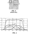
- FIG. 2 shows a pattern of red, green, and blue color filters that is commonly used.
- This particular pattern is commonly known as a Bayer color filter array (CFA) after its inventor Bryce Bayer as disclosed in US 3,971,065 .
- CFA Bayer color filter array
- This pattern is effectively used in image sensors having a two-dimensional array of color pixels.
- each pixel has a particular color photoresponse that, in this case, is a predominant sensitivity to red, green or blue light.
- Another useful variety of color photoresponses is a predominant sensitivity to magenta, yellow, or cyan light.
- the particular color photoresponse has high sensitivity to certain portions of the visible spectrum, while simultaneously having low sensitivity to other portions of the visible spectrum.
- the term color pixel will refer to a pixel having a color photoresponse.
- the set of color photoresponses selected for use in a sensor usually has three colors, as shown in the Bayer CFA, but it can also include four or more.
- a panchromatic photoresponse refers to a photoresponse having a wider spectral sensitivity than those spectral sensitivities represented in the selected set of color photoresponses.
- a panchromatic photosensitivity can have high sensitivity across the entire visible spectrum.
- panchromatic pixel will refer to a pixel having a panchromatic photoresponse.
- each panchromatic pixel can have an associated filter. Such filter is either a neutral density filter or a color filter.
- each such pattern has a repeating unit that is a contiguous subarray of pixels that acts as a basic building block.
- the entire sensor pattern is produced.
- the juxtaposition of the multiple copies of repeating units are done in diagonal directions as well as in the horizontal and vertical directions.
- a minimal repeating unit is a repeating unit such that no other repeating unit has fewer pixels.
- the CFA in FIG. 2 includes a minimal repeating unit that is two pixels by two pixels as shown by pixel block 100 in FIG. 2 . Multiple copies of this minimal repeating unit is tiled to cover the entire array of pixels in an image sensor.
- the minimal repeating unit is shown with a green pixel in the upper right corner, but three alternative minimal repeating units can easily be discerned by moving the heavy outlined area one pixel to the right, one pixel down, or one pixel diagonally to the right and down.
- pixel block 102 is a repeating unit, it is not a minimal repeating unit because pixel block 100 is a repeating unit and block 100 has fewer pixels than block 102.
- An image captured using an image sensor having a two-dimensional array with the CFA of FIG. 2 has only one color value at each pixel.
- CFA interpolation techniques are well known in the art and reference is made to the following patents: US5506619 , US5629734 , and US5652621 .
- FIG. 3 shows the relative spectral sensitivities of the pixels with red, green, and blue color filters in a typical camera application.
- the X-axis in FIG. 3 represents light wavelength in nanometers, and the Y-axis represents efficiency.
- curve 110 represents the spectral transmission characteristic of a typical filter used to block infrared and ultraviolet light from reaching the image sensor. Such a filter is needed because the color filters used for image sensors typically do not block infrared light, hence the pixels are unable to distinguish between infrared light and light that is within the passbands of their associated color filters.
- the infrared blocking characteristic shown by curve 110 prevents infrared light from corrupting the visible light signal.
- the spectral quantum efficiency i.e.
- panchromatic photoresponse is three to four times more sensitive to wide spectrum light than any of the color photoresponses.
- the greater panchromatic sensitivity shown in FIG. 3 permits improving the overall sensitivity of an image sensor by intermixing pixels that include color filters with pixels that do not include color filters.
- the color filter pixels will be significantly less sensitive than the panchromatic pixels.
- the panchromatic pixels are properly exposed to light such that the range of light intensities from a scene cover the full measurement range of the panchromatic pixels, then the color pixels will be significantly underexposed.
- the sensitivity of the color pixels are increased, for example, by increasing the size of the color pixels relative to the panchromatic pixels, with an associated reduction inspatial pixels.
- FIG. 4A represents a two-dimensional array of pixels having two groups. Pixels from the first group of pixels have a narrower spectral photoresponse than pixels from the second group of pixels.
- the first group of pixels includes individual pixels that relate to at least two different spectral photoresponses corresponding to at least two color filters. These two groups of pixels are intermixed to improve the overall sensitivity of the sensor.
- the placement of the first and second groups of pixels defines a pattern that has a minimal repeating unit including at least twelve pixels.
- the minimal repeating unit includes first and second groups of pixels arranged to permit the reproduction of a captured color image under different lighting conditions.
- the complete pattern shown in FIG. 4A represents a minimal repeating unit that is tiled to cover an entire array of pixels.
- FIG. 2 there are several other minimal repeating units that are used to describe this overall arrangement of color and panchromatic pixels, but they are all essentially equivalent in their characteristics and each is a subarray of pixels, the subarray being eight pixels by eight pixels in extent.
- An important feature of this pattern is alternating rows of panchromatic and color pixels with the color rows having pixels with the same color photoresponse grouped together.
- the groups of pixels with the same photoresponse along with some of their neighboring panchromatic pixels are considered to form four cells that make up the minimal repeating unit, a cell being a contiguous subarray of pixels having fewer pixels than a minimal repeating unit.
- These four cells delineated by heavy lines in FIG. 4A and shown as cells 120, 122, 124, and 126 in FIG. 5 , enclose four groups of four-by-four pixels each, with 120 representing the upper left cell, 122 representing the upper right cell, 124 representing the lower left cell, and 126 representing the lower right cell.
- Each of the four cells includes eight panchromatic pixels and eight color pixels of the same color photoresponse. The color pixels in a cell is combined to represent the color for that entire cell.
- cell 120 in FIG. 5 is considered to be a green cell
- cell 122 is considered to be a red cell, and so on.
- Each cell includes at least two pixels of the same color, thereby allowing pixels of the same color to be combined to overcome the difference in photosensitivity between the color pixels and the panchromatic pixels.
- the minimal repeating unit includes sixteen pixels. In the case of a minimal repeating unit with three non-overlapping cells, with each cell having two pixels of the same color and two panchromatic pixels, it is clear that the minimal repeating unit includes twelve pixels.
- the minimal repeating unit of FIG. 4A when considered in light of the cell structure identified in FIG. 5 , can represent the combination of a high-resolution panchromatic image and a low-resolution Bayer pattern color image arranged to permit the reproduction of a captured color image under different lighting conditions.
- the individual elements of the Bayer pattern image represent the combination of the color pixels in the corresponding cells.
- the first group of pixels defines a low-resolution color filter array image and the second group of pixels defines a high-resolution panchromatic image. See FIG. 6A and FIG. 6B.
- FIG. 6A represents the high-resolution panchromatic image corresponding to FIG. 4A , including both the panchromatic pixels P from FIG.
- FIG. 6B represents the low-resolution Bayer pattern color image, with R', G', and B' representing for each of the cells outlined in FIG. 5 the cell color associated with the combined color pixels in the cell.
- each cell of the pattern is rotated 90 degrees to produce the pattern shown in FIG. 4B .
- This is substantially the same pattern, but it places the highest panchromatic sampling frequency in the vertical direction instead of the horizontal direction.
- the choice to use FIG. 4A or FIG. 4B depends on whether or not it is desired to have higher panchromatic spatial sampling in either the horizontal or vertical directions respectively.
- FIG. 4A and FIG. 4B are equivalent from a color perspective.
- FIG. 4A and FIG. 4B are examples of practicing the present invention with the panchromatic pixels arranged linearly in either rows or columns.
- FIG. 4A has single rows of panchromatic pixels with each row separated from a neighboring row of panchromatic pixels by a row of color pixels;
- FIG. 4B has the same characteristic in the column direction.
- FIG. 4C represents yet another alternative minimal repeating unit to FIG. 4A with essentially the same cell color characteristics.
- FIG. 4C shows the panchromatic and color rows staggered on a cell by cell basis. This can improve the vertical panchromatic resolution.
- FIG. 4D Yet another alternative minimal repeating unit to FIG. 4A is represented in FIG. 4D , wherein the panchromatic and color rows are staggered by column pairs. This also has the potential of improving the vertical panchromatic resolution.
- a characteristic of all of the minimal repeating units of FIGS. 4A-D is that groups of two or more same color pixels are arranged side by side in either rows or columns.
- FIGS. 4A-D all have the same color structure with the cells that constitute the minimal repeating unit expressing a low-resolution Bayer pattern. It can therefore be seen that a variety of arrangements of panchromatic pixels and grouped color pixels are constructed within the scope of the claims of the present invention.
- the color pixels within each cell is combined in various ways. For example, the charge from same colored pixels are combined or binned in a CCD image sensor or in types of active pixel sensors that permit binning. Alternatively, the voltages corresponding to the measured amounts of charge in same colored pixels are averaged, for example by connecting in parallel capacitors that are charged to these voltages. In yet another approach, the digital representations of the light levels at same colored pixels are summed or averaged.
- Combining or binning charge from two pixels doubles the signal level, while the noise associated with sampling and reading out the combined signal remains the same, thereby increasing the signal to noise ratio by a factor of two, representing a corresponding two times increase in the photosensitivity of the combined pixels.
- the resulting signal increases by a factor of two, but the corresponding noise levels from reading the two pixels combine in quadrature, thereby increasing the noise by the square root of two; the resulting signal to noise ratio of the combined pixels therefore increases by the square root of two over the uncombined signals.
- a similar analysis applies to voltage or digital averaging.
- each R', G', and B' has twice the sensitivity of the uncombined pixels.
- vertically combining the charge from same colored pixels in groups of two as in FIG. 7A and horizontally summing or averaging the measured values of the combined pixels of FIG. 7A in groups of four produces the final combined color pixels of FIG. 7C , with R", G", and B" representing the final combinations of same colored pixels.
- the final combined color pixels of FIG. 7C each have four times the sensitivity of the uncombined pixels.
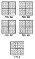
- FIG. 8A shows the cyan, magenta, and yellow equivalent of FIG. 4A , with C representing cyan pixels, M representing magenta pixels, and Y representing yellow pixels.
- the present invention is also usable with pixels having more than three color photoresponses.
- FIG. 8B shows a minimal repeating unit of the present invention that includes cyan pixels (represented by C), magenta pixels (represented by M), yellow pixels (represented by Y), and green pixels (represented by G).
- C cyan pixels
- M magenta pixels
- Y yellow pixels
- G green pixels
- FIG. 8C shows yet another alternative four color arrangement including red pixels (represented by R), blue pixels (represented by B), green pixels with one color photoresponse (represented by G), and alternative green pixels with a different color photoresponse (represented by E).
- FIG. 8D shows yet another alternative four color arrangement, wherein one of the green cells of FIG. 4A is replaced by a yellow cell, with the yellow pixels represented by Y.
- the present invention is practiced with fewer than three colors in addition to the panchromatic pixels.
- a minimal repeating unit with cells corresponding to the colors red and blue is suitable for use.
- FIG. 9 represents an alternative minimal repeating unit of the present invention with the same cell structure as FIG. 4A but with a checkerboard pattern of panchromatic pixels. This pattern provides uniform panchromatic sampling of the image, overcoming the vertical panchromatic sampling deficit of FIGS. 4A, 4C, and 4D .
- FIG. 9 is characterized as an example of practicing the present invention by arranging the panchromatic pixels in diagonal lines.
- FIG. 9 is further characterized as having single diagonal lines of panchromatic pixels with each diagonal line separated from a neighboring diagonal line of panchromatic pixels by a diagonal line of color pixels.
- Yet another characteristic of FIG. 9 is that groups two or more of same color pixels are arranged side by side in diagonal lines.
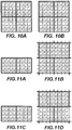
- FIG. 10A shows yet another embodiment of the present invention wherein color pixels are embedded within a grid pattern of panchromatic pixels. This pattern provides very good panchromatic spatial sampling while expressing the same color cell arrangement as FIG. 4A and 9 .
- FIG. 10B provides an example of a four color embodiment of the panchromatic grid pattern.
- the minimal repeating unit of FIG. 10 is characterized as separating each color pixel from a neighboring color pixel by one or more panchromatic pixels.
- a minimal repeating unit has been previously defined as a repeating unit such that no other repeating unit has fewer pixels.
- the sizes of repeating units from different pixel patterns are compared according to the total number of pixels in the repeating unit.
- a repeating unit that is smaller than a repeating unit having eight pixels by eight pixels contains fewer than 64 total pixels.
- the patterns presented so far have exhibited a cell structure wherein each cell contains a single color in addition to panchromatic pixels. Furthermore, all the patterns presented so far have exhibited a minimal repeating unit that is eight by eight pixels in extent.
- a minimal repeating unit can also be used that has cells with more than one color in each cell; also, a minimal repeating unit is defined that is less than eight pixels by eight pixels in extent.
- the minimal repeating unit of FIG. 11A has two cells with each cell including two colors: blue and green (represented by B and G respectively) in the left cell, and red and green (represented by R and G respectively) in the right cell. In FIG. 11A the cells contain two colors, and these colors are arranged to facilitate combining same colors for the purpose of improving color sensitivity.
- FIG. 11A the cells contain two colors, and these colors are arranged to facilitate combining same colors for the purpose of improving color sensitivity.
- FIG. 11B shows how the minimal repeating unit of FIG. 11A is tiled in order to stagger the red and blue colors.
- FIG. 11C provides a minimal repeating unit employing four colors and two colors per cell.
- FIG. 11D shows how the minimal repeating unit of FIG. 11C is tiled in order to stagger the red and blue colors.
- the coarse color pattern is characterized as a checkerboard of two different color photoresponses in the green range (represented by G and E) interleaved with a checkerboard of red and blue (represented by R and B, respectively).
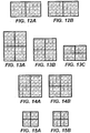
- FIG. 12A provides a panchromatic checkerboard version of FIG. 11A
- FIG. 12B provides a panchromatic checkerboard version of FIG. 11C .
- the minimal repeating units of FIGS. 11A and 11C are characterized as separating each color pixel from a neighboring color pixel in rows and columns by a dissimilar pixel, either a different color pixel or a panchromatic pixel.
- FIG. 13A is analogous to FIG. 4A , but with each color cell being 3 pixels wide by 4 pixels high and with the overall minimal repeating unit being 6 pixels wide by 8 pixels high.
- FIG. 13B eliminates two of the color pixel rows from FIG. 13A , thereby producing cells that are 3 pixels by 3 pixels and a minimal repeating unit that is 6 pixels by 6 pixels.
- FIG. 13C goes further by eliminating two of the panchromatic rows, thereby producing cells that are 3 pixels wide by 2 pixels high (with each cell containing 3 panchromatic pixels and 3 color pixels) and a minimal repeating unit that is 6 pixels wide by 4 pixels tall.
- the patterns shown in FIGS. 13A through 13C are particularly usable if the scheme for combining colors within each cell requires less than the numbers of pixels shown in FIG. 4A and other patterns.
- FIG. 14A shows yet another minimal repeating unit.
- the minimal repeating unit in FIG. 14A is six pixels by six pixels, with each cell including a 4 pixel diamond pattern of a single color with the remaining 5 pixels being panchromatic pixels.
- the panchromatic spatial sampling pattern shown in FIG. 14A is somewhat irregular, suggesting the pattern of FIG. 14B with a panchromatic checkerboard and the remaining pixels in each three pixel by three pixel cell occupied by a single color.
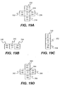
- FIG. 15A shows a minimal repeating unit that is four by four pixels and includes four two by two pixel cells. Note that each cell includes two panchromatic pixels and two same color pixels. The invention requires the placement of two same color pixels in each of the two by two cells in order to facilitate combining the color pixels within each cell.
- FIG. 15B is similar to FIG. 15A but employs a panchromatic checkerboard pattern.
- FIG. 16 the minimal repeating unit of FIG. 5 is shown subdivided into four cells, a cell being a contiguous subarray of pixels having fewer pixels than a minimal repeating unit.
- the software needed to provide the following processing is included in DSP 36 of FIG. 1 .
- Cells 220, 224, 226, and 228 are examples of cells wherein these cells contain pixels having green, red, blue and green photoresponses, respectively.
- cell 220 contains both panchromatic pixels and green pixels, the green pixels being identified as pixel group 222.
- the eventual goal is to produce a single green signal for cell 220 by combining the eight green signals from the green pixels in pixel group 222.
- a single green signal is produced by combining all eight green signals in the analog domain (e.g. by charge binning), or multiple green signals are produce by combining smaller groups of pixels taken from pixel group 222.
- the panchromatic pixels of cell 220 are shown in FIG. 17A . In the following examples, all eight signals from these panchromatic pixels are individually digitized.
- the green pixels of cell 220 are shown in FIGS. 17B-17E wherein they are grouped together according to how their signals are combined in the analog domain.
- FIG. 17B depicts the case in which all eight green pixels are combined to produce a single green signal for cell 220 ( FIG. 16 ).
- the sensor can produce two green signals, for example, by first combining the signals from pixels G21, G22, G23, and G24, and then combining the signals from pixels G41, G42, G43, and G44, as shown in FIG. 17C .
- Two signals are produced in other ways as well.
- the sensor can first combine signals from pixels G21, G22, G41, and G42, and then combine signals from pixels G23, G24, G43, and G44, as shown in FIG. 17D .
- the sensor can also produce four green signals for cell 220 by combining four pairs of signals, for example, combining pixels G21 with G22, then combining G23 with G24, then combining G41 with G42, and finally combining G43 with G44, as shown in FIG. 17E .
- cells 224, 226, and 228 For cells 224, 226, and 228 ( FIG 16 ), similar color signals are produced by the sensor depending on its mode of operation.
- the color signals for cells 224, 226, and 228 are red, blue, and green, respectively.
- the image processing algorithm of the present invention further combines the digitized green values to produce a single green value for the cell.
- One way that a single green value is obtained is by averaging all the digitized green values produced for cell 220.
- all the color data within the cell is similarly combined so that there is a single value for each color photoresponse represented within the cell.
- the digital signal processor block 36 ( FIG. 1 ) is shown receiving captured raw image data from the data bus 30 ( FIG. 1 ).
- the raw image data is passed to both the Low-resolution Partial Color block 202 and the High-resolution Panchrome block 204.
- An example of a minimal repeating unit for an image sensor has already been shown in FIG. 5 and FIG. 16 .
- the captured raw image data includes the panchromatic data that is produced by the individual panchromatic pixels as shown in FIG 17A .
- one or more green (color) values are also included, for example, from the combinations shown in FIGS. 17B-E .
- a partial color image is produced from the captured raw image data, a partial color image being a color image wherein each pixel has at least one color value and each pixel is also missing at least one color value.
- the captured raw data contains some number of color values produced by the color pixels within each cell.
- these color values are reduced to a single value for each color represented within the cell. For the cell 220 ( FIG. 16 ), as an example, a single green color value is produced.
- cells 224, 226 and 228, a single red, blue and green color value is produced, respectively.
- the Low-resolution Partial Color block 202 processes each cell in a similar manner resulting in an array of color values, one for each cell. Because the resulting image array based on cells rather than pixels in the original sensor, it is four times smaller in each dimension than the original captured raw image data array. Because the resulting array is based on cells and because each pixel has some but not all color values, the resulting image is a low-resolution partial color image. At this point, the low-resolution partial color image is color balanced.
- panchromatic values must be estimated for the green pixels in pixel group 222 ( FIG. 16 ).
- panchromatic value is to do vertical averaging.
- we can estimate the panchromatic value at pixel 22 as follows: P 22 P 12 + P 32 / 2
- an adaptive method can also be used.
- panchromatic interpolation is continued throughout the image without regard to cell boundaries.
- the processing of High-resolution Panchrome block 204 is done, the resulting digital panchromatic image is the same size as the original captured raw image, which makes it a high-resolution panchromatic image.
- the Low-resolution Panchrome block 206 receives the high-resolution panchromatic image array produced by block 204 and generates a low-resolution panchromatic image array which is the same size as the low-resolution partial color image produced by block 202.
- Each low-resolution panchromatic value is obtained by averaging the estimated panchromatic values, within a given cell, for those pixels having color filters.
- the high-resolution panchromatic values previously estimated for the green pixels in pixel group 222 ( FIG. 16 ) are now averaged together to produce a single low-resolution panchromatic value for the cell.
- a single low-resolution panchromatic value is computed for cell 224 using high-resolution panchromatic values estimated at the pixels having red filters. In this manner, each cell ends up with a single low-resolution panchromatic value.
- the Low-resolution Color Difference block 208 receives the low-resolution partial color image from block 202 and the low-resolution panchrome array from block 206. A low-resolution intermediate color image is then formed by color interpolating the low-resolution partial color image with guidance from the low-resolution panchrome image. The exact nature of the color interpolation algorithm, to be discussed in detail later, depends on which pattern of pixel photoresponses was used to capture the original raw image data.
- the High-resolution Color Difference block 210 receives the low-resolution color difference image from block 208 and, using bilinear interpolation, upsamples the low-resolution color difference image to match the size of the original raw image data. The result is a high-resolution color difference image that is the same size as the high-resolution panchromatic image produced by block 204.
- the High-resolution Final Image block 212 receives the high-resolution color difference image from block 210 and the high-resolution panchromatic image from block 204.
- a high-resolution final color image is then formed by adding the high-resolution panchromatic image to each of the high-resolution color difference planes.
- the resulting high-resolution final color image can then be further processed. For example, it is stored in the DSP Memory block 32 ( FIG. 1 ) and then sharpened and compressed for storage on the Memory Card block 64 ( FIG. 1 ).
- the sensor filter patterns shown in FIGS. 4A-D , 8A , 9 , 10A , 13A-C, 14A-B and 15A-B have a minimal repeating unit such that the resulting low-resolution partial color image, produced in block 202, exhibits the repeating Bayer pattern for color filters:
- Color interpolation begins by interpolating the green values at pixels not already having green values, shown as pixel234 in FIG. 19A .
- the four neighboring pixels shown as pixels 230, 232, 236, and 238, all have green values and they also all have panchromatic values.
- the center pixel 234 has a panchromatic value, but does not have a green value as indicated by the question marks.
- the first step is to compute two classifier values, the first relating to the horizontal direction, and the second to the vertical direction:
- HCLAS ABS P 4 ⁇ P 2 + ABS 2 * P 3 ⁇ P 2 ⁇ P 4
- VCLAS ABS P 5 ⁇ P 1 + ABS 2 * P 3 ⁇ P 1 ⁇ P 5
- HPRED G 4 + G 2 / 2 + 2 * P 3 ⁇ P 2 ⁇ P 4 / 2
- VPRED G 5 + G 1 / 2 + 2 * P 3 ⁇ P 1 ⁇ P 5 / 2
- THRESH be an empirically determined threshold value
- red and blue values are interpolated.
- pixel 242 is missing a red value but its two horizontal neighbors, pixels 240 and 244, have red values R2 and R4 respectively. All three pixels have green values.
- Missing blue values are computed in a similar way under similar conditions. This completes the interpolation of the low-resolution partial color image and the result is a low-resolution intermediate color image. As described earlier, the low-resolution color differences can now be computed by subtracting the low-resolution panchrome values from each color plane: red, green, and blue in the example just discussed.
- the sensor pattern shown in FIG. 11A determines that each cell receives two color values: either green and red, or green and blue. Consequently, in this case, the color interpolation task within the Low-resolution Color Differences block 208 ( FIG. 18 ) estimates missing values of red or missing values of blue for each pixel.
- a pixel 264 is shown having a green value (G3) but not having a red value (R3).
- R3 red value
- Four of the neighboring pixels 260, 262, 266, and 268 have green values and red values.
- the method for interpolating the red value for pixel 264 ( FIG. 19D ) is similar to the method used to interpolate the green value for pixel 234 ( FIG. 19A ).
- the first step is to compute two classifier values, the first relating to the horizontal direction, and the second to the vertical direction:
- HCLAS ABS G 4 ⁇ G 2 + ABS 2 * G 3 ⁇ G 2 ⁇ G 4
- VCLAS ABS G 5 ⁇ G 1 + ABS 2 * G 3 ⁇ G 1 ⁇ G 5
- HPRED R 4 + R 2 / 2 + 2 * G 3 ⁇ G 2 ⁇ G 4 / 2
- VPRED R 5 + R 1 / 2 + 2 * G 3 ⁇ G 1 ⁇ G 5 / 2
- the missing value G3 is computed adaptively according to:
- the missing blue values are interpolated in exactly the same way using blue values in place of red.
- the low-resolution intermediate color image has been produced. From there, the low-resolution color differences are computed as previously described.
Landscapes
- Engineering & Computer Science (AREA)
- Multimedia (AREA)
- Signal Processing (AREA)
- Physics & Mathematics (AREA)
- Spectroscopy & Molecular Physics (AREA)
- Color Television Image Signal Generators (AREA)
- Facsimile Image Signal Circuits (AREA)
- Color Image Communication Systems (AREA)
- Image Processing (AREA)
- Editing Of Facsimile Originals (AREA)
Claims (3)
- Verfahren zur Ausbildung eines digitalen Farbbildes, umfassend:a) Aufnahme eines Bildes unter Anwendung eines Halbleiterbildsensors (20), der eine Pixelanordnung aufweist, die sowohl panchromatische Pixel als auch Farbpixel umfasst, welche innerhalb eines einzelnen Pixelmusters des Halbleiterbildsensors (20) bereitgestellt sind, worin die Farbpixel mindestens zwei Farbfotoempfindlichkeiten entsprechen, wobei eine Farbfotoempfindlichkeit eine vorherrschende Empfindlichkeit für eine Farbe ist;b) worin die Pixelanordnung aus einer Vielzahl von in Felder aufgeteilten, kleinsten wiederkehrenden Einheiten gebildet ist, wobei jede kleinste wiederkehrende Einheit eine Vielzahl von Zellen umfasst, wobei jede Zelle mindestens zwei panchromatische Pixel und mindestens zwei Pixel, welche dieselbe Farbfotoempfindlichkeit aufweisen, umfasst, worin das aufgenommene Bild eine Anzahl von durch die Farbpixel innerhalb jeder Zelle erzeugten Farbwerten enthält;c) Bereitstellen von Bilddaten aus dem aufgenommenen Bild;dadurch gekennzeichnet, dass:d) die Bilddaten sowohl an einen Teilfarbenblock mit niedriger Auflösung (202) als auch an einen Panchromatischen Block mit hoher Auflösung (204) übermittelt werden;e) im Teilfarbenblock mit niedriger Auflösung (202) die Anzahl von Farbwerten innerhalb jeder Zelle auf einen einzigen Wert für jede Farbe, die innerhalb der Zelle dargestellt ist, reduziert ist, wodurch ein Teilfarbenbild mit niedriger Auflösung von dem aufgenommenen Bild erzeugt wird, wobei ein Teilfarbenbild ein Farbbild ist, worin jedes Pixel einer Zelle entspricht und mindestens einen Farbenwert aufweist und auch mindestens einen Farbenwert nicht aufweist;f) die Bilddaten auch an den Panchromatischen Block mit hoher Auflösung (204) weitergeleitet werden, was ein vollständiges panchromatisches Bild mit hoher Auflösung unter Anwendung lediglich der panchromatischen Werte in den Bilddaten erzeugt, um panchromatische Werte bei denjenigen Pixeln zu schätzen, die noch keine panchromatischen Werte aufweisen;g) an einem Panchromatischen Block mit niedriger Auflösung (206) das durch den Panchromatischen Block mit hoher Auflösung (204) erzeugte panchromatische Bild mit hoher Auflösung empfangen wird und ein panchromatisches Bild mit niedriger Auflösung erzeugt wird, indem für jede Zelle der Mittelwert für die zuvor geschätzten panchromatischen Werte innerhalb der Zelle gebildet wird, um einen einzelnen panchromatischen Wert mit niedriger Auflösung für die Zelle zu erzielen, worin das panchromatische Bild mit niedriger Auflösung dieselbe Auflösung wie das durch den Teilfarbenblock mit niedriger Auflösung (202) erzeugte Teilfarbenbild mit niedriger Auflösung aufweist;h) an einem Farbdifferenzblock mit niedriger Auflösung (208) das Teilfarbenbild mit niedriger Auflösung aus dem Teilfarbenblock mit niedriger Auflösung (202) und ein panchromatisches Bild mit niedriger Auflösung aus dem Panchromatischen Block mit niedriger Auflösung (206) empfangen wird, ein Zwischenfarbenbild mit niedriger Auflösung durch Farbinterpolieren des Teilfarbenbildes mit niedriger Auflösung auf Basis des panchromatischen Bildes mit niedriger Auflösung unter Anwendung eines Farbinterpolationsalgorithmus ausgebildet wird, und dann ein Farbdifferenzbild mit niedriger Auflösung durch Subtrahieren des panchromatischen Bildes mit niedriger Auflösung von jeder Farbebene des Zwischenfarbenbildes mit niedriger Auflösung berechnet wird;i) an einem Farbdifferenzblock mit hoher Auflösung (210) das Farbdifferenzbild mit niedriger Auflösung aus dem Farbdifferenzblock mit niedriger Auflösung (208) empfangen wird und das Farbdifferenzbild mit niedriger Auflösung abtastratenmäßig erhöht wird, um der Auflösung der ursprünglichen Bilddaten zu entsprechen, um ein Farbdifferenzbild mit hoher Auflösung zu erzeugen, das dieselbe Auflösung wie das durch den Panchromatischen Block mit hoher Auflösung (204) erzeugte panchromatische Bild mit hoher Auflösung ist;j) an einem Letzten Bildblock mit hoher Auflösung (212) das panchromatische Bild mit hoher Auflösung aus dem Panchromatischen Block mit hoher Auflösung (204) und das Farbdifferenzbild mit hoher Auflösung aus dem Farbdifferenzblock mit hoher Auflösung (210) empfangen wird, und ein endgültiges Farbbild mit hoher Auflösung durch Hinzufügen des panchromatischen Bildes mit hoher Auflösung zu jeder Farbebene des Farbdifferenzbildes mit hoher Auflösung ausgebildet wird.
- Verfahren nach Anspruch 1, worin das Pixelmuster des Bildsensors (20) eine kleinste wiederkehrende Einheit aufweist, die mindestens zwölf Pixel umfasst.
- Verfahren nach Anspruch 2, worin die kleinste wiederkehrende Einheit mindestens zwei nicht-überlappende Zellen (220, 224, 226, 228) umfasst, die jeweils mindestens zwei panchromatische Pixel und mindestens zwei Farbpixel, welche dieselbe spektrale Fotoempfindlichkeit aufweisen, aufweisen.
Applications Claiming Priority (2)
| Application Number | Priority Date | Filing Date | Title |
|---|---|---|---|
| US11/191,538 US8274715B2 (en) | 2005-07-28 | 2005-07-28 | Processing color and panchromatic pixels |
| PCT/US2006/028493 WO2007015982A2 (en) | 2005-07-28 | 2006-07-20 | Processing color and panchromatic pixels |
Publications (2)
| Publication Number | Publication Date |
|---|---|
| EP1908301A2 EP1908301A2 (de) | 2008-04-09 |
| EP1908301B1 true EP1908301B1 (de) | 2017-08-23 |
Family
ID=37441623
Family Applications (1)
| Application Number | Title | Priority Date | Filing Date |
|---|---|---|---|
| EP06788192.0A Active EP1908301B1 (de) | 2005-07-28 | 2006-07-20 | Verarbeiten von farb- und panchromatischen pixeln |
Country Status (5)
| Country | Link |
|---|---|
| US (2) | US8274715B2 (de) |
| EP (1) | EP1908301B1 (de) |
| JP (1) | JP4971323B2 (de) |
| CN (1) | CN101233763B (de) |
| WO (1) | WO2007015982A2 (de) |
Families Citing this family (138)
| Publication number | Priority date | Publication date | Assignee | Title |
|---|---|---|---|---|
| US8274715B2 (en) | 2005-07-28 | 2012-09-25 | Omnivision Technologies, Inc. | Processing color and panchromatic pixels |
| US8139130B2 (en) | 2005-07-28 | 2012-03-20 | Omnivision Technologies, Inc. | Image sensor with improved light sensitivity |
| US7636115B2 (en) * | 2005-08-11 | 2009-12-22 | Aptina Imaging Corporation | High dynamic range imaging device using multiple pixel cells |
| JP4730082B2 (ja) * | 2005-12-22 | 2011-07-20 | ソニー株式会社 | 画像信号処理装置、撮像装置、および画像信号処理方法、並びにコンピュータ・プログラム |
| US7688368B2 (en) | 2006-01-27 | 2010-03-30 | Eastman Kodak Company | Image sensor with improved light sensitivity |
| US7916362B2 (en) * | 2006-05-22 | 2011-03-29 | Eastman Kodak Company | Image sensor with improved light sensitivity |
| JP4855155B2 (ja) * | 2006-06-27 | 2012-01-18 | 株式会社リコー | 撮像装置及びこれを用いた撮影方法 |
| US8031258B2 (en) | 2006-10-04 | 2011-10-04 | Omnivision Technologies, Inc. | Providing multiple video signals from single sensor |
| US7876956B2 (en) * | 2006-11-10 | 2011-01-25 | Eastman Kodak Company | Noise reduction of panchromatic and color image |
| JP4930109B2 (ja) | 2007-03-06 | 2012-05-16 | ソニー株式会社 | 固体撮像装置、撮像装置 |
| US7913922B1 (en) | 2007-03-15 | 2011-03-29 | Ncr Corporation | Matching bar code colors to painted pixel filters |
| US8594451B2 (en) * | 2007-03-30 | 2013-11-26 | Omnivision Technologies, Inc. | Edge mapping incorporating panchromatic pixels |
| US7844127B2 (en) * | 2007-03-30 | 2010-11-30 | Eastman Kodak Company | Edge mapping using panchromatic pixels |
| US7889921B2 (en) * | 2007-05-23 | 2011-02-15 | Eastman Kodak Company | Noise reduced color image using panchromatic image |
| JP5222625B2 (ja) * | 2007-06-01 | 2013-06-26 | 富士フイルム株式会社 | 撮像装置 |
| JP5033711B2 (ja) * | 2007-06-13 | 2012-09-26 | 富士フイルム株式会社 | 撮像装置及び撮像装置の駆動方法 |
| JP5250315B2 (ja) * | 2007-06-28 | 2013-07-31 | 富士フイルム株式会社 | 信号処理装置、撮像装置、及び同時化処理プログラム |
| US20090046182A1 (en) * | 2007-08-14 | 2009-02-19 | Adams Jr James E | Pixel aspect ratio correction using panchromatic pixels |
| US8452082B2 (en) * | 2007-09-27 | 2013-05-28 | Eastman Kodak Company | Pattern conversion for interpolation |
| US7999870B2 (en) * | 2008-02-01 | 2011-08-16 | Omnivision Technologies, Inc. | Sampling and readout of an image sensor having a sparse color filter array pattern |
| US8035716B2 (en) * | 2008-06-13 | 2011-10-11 | Omnivision Technologies, Inc. | Wide aperture image sensor pixel |
| US7915067B2 (en) * | 2008-07-09 | 2011-03-29 | Eastman Kodak Company | Backside illuminated image sensor with reduced dark current |
| US7859033B2 (en) | 2008-07-09 | 2010-12-28 | Eastman Kodak Company | Wafer level processing for backside illuminated sensors |
| US8587681B2 (en) * | 2008-11-21 | 2013-11-19 | Omnivision Technologies, Inc. | Extended depth of field for image sensor |
| CN106137138A (zh) * | 2009-01-07 | 2016-11-23 | 基文影像公司 | 用于检测体内病变的装置和方法 |
| JP5545612B2 (ja) * | 2009-01-14 | 2014-07-09 | 富士フイルム株式会社 | 画像処理システム、画像処理方法、及びプログラム |
| EP2380345B1 (de) | 2009-01-16 | 2016-10-26 | Dual Aperture International Co. Ltd. | Verbessern der schärfentiefe eines bildgebungssystems |
| DE102009001122B8 (de) | 2009-02-24 | 2020-11-26 | Robert Bosch Gmbh | Kameraanordnung und Verfahren zum Ermitteln von Bildsignalen mit Farbwerten |
| US8224082B2 (en) * | 2009-03-10 | 2012-07-17 | Omnivision Technologies, Inc. | CFA image with synthetic panchromatic image |
| US8068153B2 (en) * | 2009-03-27 | 2011-11-29 | Omnivision Technologies, Inc. | Producing full-color image using CFA image |
| US8218068B2 (en) * | 2009-04-01 | 2012-07-10 | Omnivision Technologies, Inc. | Exposing pixel groups in producing digital images |
| US8045024B2 (en) * | 2009-04-15 | 2011-10-25 | Omnivision Technologies, Inc. | Producing full-color image with reduced motion blur |
| US8203633B2 (en) * | 2009-05-27 | 2012-06-19 | Omnivision Technologies, Inc. | Four-channel color filter array pattern |
| US8237831B2 (en) * | 2009-05-28 | 2012-08-07 | Omnivision Technologies, Inc. | Four-channel color filter array interpolation |
| US8125546B2 (en) * | 2009-06-05 | 2012-02-28 | Omnivision Technologies, Inc. | Color filter array pattern having four-channels |
| US8253832B2 (en) * | 2009-06-09 | 2012-08-28 | Omnivision Technologies, Inc. | Interpolation for four-channel color filter array |
| JP5326943B2 (ja) * | 2009-08-31 | 2013-10-30 | ソニー株式会社 | 画像処理装置、および画像処理方法、並びにプログラム |
| JP5454075B2 (ja) | 2009-10-20 | 2014-03-26 | ソニー株式会社 | 画像処理装置、および画像処理方法、並びにプログラム |
| US20110157395A1 (en) | 2009-12-31 | 2011-06-30 | Compton John T | Image sensor with fractional resolution image processing |
| JP5724185B2 (ja) | 2010-03-04 | 2015-05-27 | ソニー株式会社 | 画像処理装置、および画像処理方法、並びにプログラム |
| US9280768B2 (en) * | 2010-03-17 | 2016-03-08 | Verifone, Inc. | Payment systems and methodologies |
| US8619143B2 (en) * | 2010-03-19 | 2013-12-31 | Pixim, Inc. | Image sensor including color and infrared pixels |
| DE102010003668B4 (de) * | 2010-04-07 | 2020-03-26 | Robert Bosch Gmbh | Farbmaske für einen Bildsensor einer Fahrzeugkamera |
| US8345117B2 (en) * | 2010-06-30 | 2013-01-01 | Hand Held Products, Inc. | Terminal outputting monochrome image data and color image data |
| US9739914B2 (en) | 2010-07-13 | 2017-08-22 | Nokia Technologies Oy | Color image sensing |
| EP2702375A2 (de) * | 2011-04-25 | 2014-03-05 | Skybox Imaging, Inc. | Systeme und verfahren für overhead-bildgebung und video |
| EP2721828B1 (de) | 2011-06-15 | 2015-07-15 | Microsoft Technology Licensing, LLC | Hochauflösende multispektrale bilderfassung |
| JP2013183353A (ja) * | 2012-03-02 | 2013-09-12 | Toshiba Corp | 画像処理装置 |
| JP6131546B2 (ja) * | 2012-03-16 | 2017-05-24 | 株式会社ニコン | 画像処理装置、撮像装置および画像処理プログラム |
| JP5935876B2 (ja) * | 2012-03-27 | 2016-06-15 | ソニー株式会社 | 画像処理装置、撮像素子、および画像処理方法、並びにプログラム |
| DE102012110092A1 (de) * | 2012-10-23 | 2014-04-24 | Conti Temic Microelectronic Gmbh | Sensoranordnung zur Bilderfassung |
| KR101444263B1 (ko) * | 2012-12-04 | 2014-09-30 | (주)실리콘화일 | 분광특성이 강화된 적외선 픽셀을 구비한 씨모스 이미지센서 및 그 제조방법 |
| JP6308760B2 (ja) * | 2012-12-20 | 2018-04-11 | キヤノン株式会社 | 光電変換装置および光電変換装置を有する撮像装置 |
| US9293500B2 (en) | 2013-03-01 | 2016-03-22 | Apple Inc. | Exposure control for image sensors |
| US9276031B2 (en) | 2013-03-04 | 2016-03-01 | Apple Inc. | Photodiode with different electric potential regions for image sensors |
| US9741754B2 (en) | 2013-03-06 | 2017-08-22 | Apple Inc. | Charge transfer circuit with storage nodes in image sensors |
| US9549099B2 (en) | 2013-03-12 | 2017-01-17 | Apple Inc. | Hybrid image sensor |
| US9319611B2 (en) | 2013-03-14 | 2016-04-19 | Apple Inc. | Image sensor with flexible pixel summing |
| GB2526217B (en) * | 2013-03-15 | 2020-11-04 | Intel Corp | Mobile computing device technology and systems and methods utilizing the same |
| US10027930B2 (en) | 2013-03-29 | 2018-07-17 | Magna Electronics Inc. | Spectral filtering for vehicular driver assistance systems |
| US9491377B2 (en) | 2013-08-07 | 2016-11-08 | Trimble Navigation Limited | Methods of extracting 4-band data from a single CCD; methods of generating 4×4 or 3×3 color correction matrices using a single CCD |
| US9596423B1 (en) | 2013-11-21 | 2017-03-14 | Apple Inc. | Charge summing in an image sensor |
| US9596420B2 (en) | 2013-12-05 | 2017-03-14 | Apple Inc. | Image sensor having pixels with different integration periods |
| US9473706B2 (en) | 2013-12-09 | 2016-10-18 | Apple Inc. | Image sensor flicker detection |
| US10285626B1 (en) | 2014-02-14 | 2019-05-14 | Apple Inc. | Activity identification using an optical heart rate monitor |
| US9277144B2 (en) | 2014-03-12 | 2016-03-01 | Apple Inc. | System and method for estimating an ambient light condition using an image sensor and field-of-view compensation |
| US9584743B1 (en) | 2014-03-13 | 2017-02-28 | Apple Inc. | Image sensor with auto-focus and pixel cross-talk compensation |
| US9538106B2 (en) | 2014-04-25 | 2017-01-03 | Apple Inc. | Image sensor having a uniform digital power signature |
| US9686485B2 (en) | 2014-05-30 | 2017-06-20 | Apple Inc. | Pixel binning in an image sensor |
| WO2015192056A1 (en) | 2014-06-13 | 2015-12-17 | Urthecast Corp. | Systems and methods for processing and providing terrestrial and/or space-based earth observation video |
| US8908986B1 (en) | 2014-07-23 | 2014-12-09 | Teespring, Inc. | Systems and methods for selecting ink colors |
| US9225889B1 (en) | 2014-08-18 | 2015-12-29 | Entropix, Inc. | Photographic image acquisition device and method |
| US9479745B2 (en) | 2014-09-19 | 2016-10-25 | Omnivision Technologies, Inc. | Color filter array with reference pixel to reduce spectral crosstalk |
| US9866764B2 (en) | 2014-11-21 | 2018-01-09 | Motorola Mobility Llc | Method and apparatus for synchronizing auto exposure between chromatic pixels and panchromatic pixels in a camera system |
| DE112014007038T5 (de) * | 2014-11-28 | 2017-08-10 | Olympus Corporation | Endoskopvorrichtung |
| US10410398B2 (en) * | 2015-02-20 | 2019-09-10 | Qualcomm Incorporated | Systems and methods for reducing memory bandwidth using low quality tiles |
| US20160255323A1 (en) | 2015-02-26 | 2016-09-01 | Dual Aperture International Co. Ltd. | Multi-Aperture Depth Map Using Blur Kernels and Down-Sampling |
| CA2980920C (en) | 2015-03-25 | 2023-09-26 | King Abdulaziz City Of Science And Technology | Apparatus and methods for synthetic aperture radar with digital beamforming |
| JP6622481B2 (ja) * | 2015-04-15 | 2019-12-18 | キヤノン株式会社 | 撮像装置、撮像システム、撮像装置の信号処理方法、信号処理方法 |
| WO2017044168A2 (en) | 2015-06-16 | 2017-03-16 | King Abdulaziz City Of Science And Technology | Efficient planar phased array antenna assembly |
| US9467665B1 (en) * | 2015-06-29 | 2016-10-11 | Omnivision Technologies, Inc. | Color filter array patterns for reduction of color aliasing |
| KR102329440B1 (ko) * | 2015-10-01 | 2021-11-19 | 에스케이하이닉스 주식회사 | 칼라 필터 어레이의 변환 방법 및 장치 |
| US9686478B2 (en) | 2015-11-19 | 2017-06-20 | Google Inc. | Generating high-dynamic range images using multiple filters |
| US9674460B1 (en) | 2015-11-19 | 2017-06-06 | Google Inc. | Generating high-dynamic range images using varying exposures |
| EP3380864A4 (de) | 2015-11-25 | 2019-07-03 | Urthecast Corp. | Radarbildgebungsvorrichtung mit synthetischer apertur und verfahren |
| JP2017099616A (ja) * | 2015-12-01 | 2017-06-08 | ソニー株式会社 | 手術用制御装置、手術用制御方法、およびプログラム、並びに手術システム |
| US10223061B2 (en) * | 2015-12-17 | 2019-03-05 | International Business Machines Corporation | Display redistribution between a primary display and a secondary display |
| WO2017149932A1 (ja) * | 2016-03-03 | 2017-09-08 | ソニー株式会社 | 医療用画像処理装置、システム、方法及びプログラム |
| WO2017156566A1 (en) | 2016-03-15 | 2017-09-21 | Tech Plas Extrusions Pty Ltd | A scaffold board |
| US9912883B1 (en) | 2016-05-10 | 2018-03-06 | Apple Inc. | Image sensor with calibrated column analog-to-digital converters |
| US10341628B2 (en) * | 2016-08-08 | 2019-07-02 | Google Llc | Monochrome-color mapping using a monochromatic imager and a color map sensor |
| DE102016217282A1 (de) | 2016-09-12 | 2018-03-15 | Conti Temic Microelectronic Gmbh | Bildsensor, bilderfassungsvorrichtung, fahrerassistenzsystem, fahrzeug und verfahren zur auswertung von elektromagnetischer strahlung |
| CN111682039B (zh) | 2016-09-23 | 2021-08-03 | 苹果公司 | 堆叠式背面照明spad阵列 |
| EP3565259A1 (de) * | 2016-12-28 | 2019-11-06 | Panasonic Intellectual Property Corporation of America | Verteilungsverfahren für dreidimensionales modell, empfangsverfahren für dreidimensionales modell, verteilungsvorrichtung für dreidimensionales modell und empfangsvorrichtung für dreidimensionales modell |
| JP6799690B2 (ja) | 2017-01-25 | 2020-12-16 | アップル インコーポレイテッドApple Inc. | 変調感度を有するspad検出器 |
| US10656251B1 (en) | 2017-01-25 | 2020-05-19 | Apple Inc. | Signal acquisition in a SPAD detector |
| US10962628B1 (en) | 2017-01-26 | 2021-03-30 | Apple Inc. | Spatial temporal weighting in a SPAD detector |
| EP3631504B8 (de) | 2017-05-23 | 2023-08-16 | Spacealpha Insights Corp. | Radarbildgebungsvorrichtung mit synthetischer apertur und verfahren |
| WO2018217902A1 (en) | 2017-05-23 | 2018-11-29 | King Abdullah City Of Science And Technology | Synthetic aperture radar imaging apparatus and methods for moving targets |
| US10474908B2 (en) * | 2017-07-06 | 2019-11-12 | GM Global Technology Operations LLC | Unified deep convolutional neural net for free-space estimation, object detection and object pose estimation |
| US10622538B2 (en) | 2017-07-18 | 2020-04-14 | Apple Inc. | Techniques for providing a haptic output and sensing a haptic input using a piezoelectric body |
| US10440301B2 (en) | 2017-09-08 | 2019-10-08 | Apple Inc. | Image capture device, pixel, and method providing improved phase detection auto-focus performance |
| CA3083033A1 (en) | 2017-11-22 | 2019-11-28 | Urthecast Corp. | Synthetic aperture radar apparatus and methods |
| JP7349806B2 (ja) * | 2018-03-28 | 2023-09-25 | ブラックマジック デザイン ピーティーワイ リミテッド | 画像処理方法及びフィルタアレイ |
| US11019294B2 (en) | 2018-07-18 | 2021-05-25 | Apple Inc. | Seamless readout mode transitions in image sensors |
| US10848693B2 (en) | 2018-07-18 | 2020-11-24 | Apple Inc. | Image flare detection using asymmetric pixels |
| US10841488B2 (en) * | 2018-08-03 | 2020-11-17 | Qualcomm Incorporated | Combined monochrome and chromatic camera sensor |
| CN114422766B (zh) * | 2018-08-03 | 2024-06-04 | 杭州海康威视数字技术股份有限公司 | 一种图像采集设备 |
| US10750108B2 (en) | 2018-09-25 | 2020-08-18 | Omnivision Technologies, Inc. | Image sensor with correction of non-uniform dark current |
| WO2020244765A1 (en) * | 2019-06-06 | 2020-12-10 | Huawei Technologies Co., Ltd. | Color filter array apparatus |
| US10819927B1 (en) | 2019-07-02 | 2020-10-27 | Omnivision Technologies, Inc. | Image sensor with self-testing black level correction |
| WO2021046690A1 (zh) | 2019-09-09 | 2021-03-18 | Oppo广东移动通信有限公司 | 图像传感器、摄像头模组、移动终端及图像采集方法 |
| CN110649056B (zh) * | 2019-09-30 | 2022-02-18 | Oppo广东移动通信有限公司 | 图像传感器、摄像头组件及移动终端 |
| EP4033535B1 (de) | 2019-09-30 | 2025-09-10 | Guangdong Oppo Mobile Telecommunications Corp., Ltd. | Bildsensor, kameraanordnung und mobiles endgerät |
| CN114008782B (zh) * | 2019-09-30 | 2026-02-24 | Oppo广东移动通信有限公司 | 图像传感器、摄像头组件及移动终端 |
| CN114008781B (zh) * | 2019-09-30 | 2026-04-17 | Oppo广东移动通信有限公司 | 图像传感器、摄像头组件及移动终端 |
| CN110649057B (zh) * | 2019-09-30 | 2021-03-05 | Oppo广东移动通信有限公司 | 图像传感器、摄像头组件及移动终端 |
| CN111050041B (zh) * | 2019-11-25 | 2021-03-26 | Oppo广东移动通信有限公司 | 图像传感器、控制方法、摄像头组件及移动终端 |
| US12273633B2 (en) | 2020-02-19 | 2025-04-08 | Sony Group Corporation | Image processing method and sensor device for performing coloring processing on an image signal acquired using an array sensor |
| CN111405204B (zh) * | 2020-03-11 | 2022-07-26 | Oppo广东移动通信有限公司 | 图像获取方法、成像装置、电子设备及可读存储介质 |
| CN111385543B (zh) * | 2020-03-13 | 2022-02-18 | Oppo广东移动通信有限公司 | 图像传感器、摄像头组件、移动终端及图像获取方法 |
| CN111314592B (zh) * | 2020-03-17 | 2021-08-27 | Oppo广东移动通信有限公司 | 图像处理方法、摄像头组件及移动终端 |
| CN111510692B (zh) * | 2020-04-23 | 2022-01-18 | Oppo广东移动通信有限公司 | 图像处理方法、终端及计算机可读存储介质 |
| CN111586375B (zh) * | 2020-05-08 | 2021-06-11 | Oppo广东移动通信有限公司 | 高动态范围图像处理系统及方法、电子设备和可读存储介质 |
| CN111711766B (zh) * | 2020-06-17 | 2022-01-04 | Oppo广东移动通信有限公司 | 图像处理方法及装置、终端和计算机可读存储介质 |
| CN111741221B (zh) | 2020-07-08 | 2021-04-09 | Oppo广东移动通信有限公司 | 图像获取方法、摄像头组件及移动终端 |
| CN113766231B (zh) * | 2020-07-08 | 2025-06-10 | Oppo广东移动通信有限公司 | 图像获取方法、摄像头组件及移动终端 |
| US11563910B2 (en) | 2020-08-04 | 2023-01-24 | Apple Inc. | Image capture devices having phase detection auto-focus pixels |
| CN112235485B (zh) * | 2020-10-09 | 2023-04-07 | Oppo广东移动通信有限公司 | 图像传感器、图像处理方法、成像装置、终端及可读存储介质 |
| CN112261391B (zh) * | 2020-10-26 | 2022-01-04 | Oppo广东移动通信有限公司 | 图像处理方法、摄像头组件及移动终端 |
| US11546532B1 (en) | 2021-03-16 | 2023-01-03 | Apple Inc. | Dynamic correlated double sampling for noise rejection in image sensors |
| US20220344382A1 (en) * | 2021-04-22 | 2022-10-27 | Taiwan Semiconductor Manufacturing Company, Ltd. | Deep trench isolation structure in a pixel sensor |
| WO2022262997A1 (en) * | 2021-06-18 | 2022-12-22 | Huawei Technologies Co., Ltd. | A device and method for creating a high-dynamic range colour image |
| US12192644B2 (en) | 2021-07-29 | 2025-01-07 | Apple Inc. | Pulse-width modulation pixel sensor |
| CN113840067B (zh) * | 2021-09-10 | 2023-08-18 | Oppo广东移动通信有限公司 | 图像传感器、图像生成方法、装置和电子设备 |
| US12069384B2 (en) | 2021-09-23 | 2024-08-20 | Apple Inc. | Image capture devices having phase detection auto-focus pixels |
| CN114125240A (zh) * | 2021-11-30 | 2022-03-01 | 维沃移动通信有限公司 | 图像传感器、摄像模组、电子设备及拍摄方法 |
| US20230196621A1 (en) * | 2021-12-17 | 2023-06-22 | Meta Platforms Technologies, Llc | Sparse rgb filter hardware accelerator |
Family Cites Families (315)
| Publication number | Priority date | Publication date | Assignee | Title |
|---|---|---|---|---|
| US2508267A (en) | 1945-10-26 | 1950-05-16 | Du Mont Allen B Lab Inc | Color television |
| US2446791A (en) | 1946-06-11 | 1948-08-10 | Rca Corp | Color television tube |
| US2884483A (en) | 1955-03-09 | 1959-04-28 | Grimson Color Inc | Color image pick up apparatus |
| JPS5016134B1 (de) | 1970-12-26 | 1975-06-11 | ||
| US3971065A (en) * | 1975-03-05 | 1976-07-20 | Eastman Kodak Company | Color imaging array |
| JPS6056030B2 (ja) | 1975-10-24 | 1985-12-07 | 松下電器産業株式会社 | カラー固体撮像装置 |
| US4047203A (en) | 1976-05-12 | 1977-09-06 | Eastman Kodak Company | Color imaging array |
| US4437112A (en) | 1980-02-15 | 1984-03-13 | Canon Kabushiki Kaisha | Solid-state color imaging apparatus |
| JPS5763983A (en) * | 1980-10-07 | 1982-04-17 | Toshiba Corp | Color image pickup device |
| US4500914A (en) | 1981-08-01 | 1985-02-19 | Sharp Kabushiki Kaisha | Color imaging array and color imaging device |
| US4591900A (en) | 1983-03-14 | 1986-05-27 | Rca Corporation | Encoding pattern for single chip CCD camera processing scheme |
| EP0119862B1 (de) | 1983-03-17 | 1990-12-27 | Nec Corporation | Festkörperfarbabbildungsgerät |
| JPS6020111A (ja) | 1983-07-14 | 1985-02-01 | Fuji Electric Corp Res & Dev Ltd | 距離測定装置 |
| EP0138074B1 (de) | 1983-09-16 | 1989-12-13 | Hitachi, Ltd. | Signalverarbeitungsschaltung für eine Farbvideokamera |
| JPS60103790A (ja) | 1983-11-10 | 1985-06-08 | Nec Corp | カラ−固体撮像装置 |
| JPS60226282A (ja) | 1984-04-24 | 1985-11-11 | Canon Inc | 撮像装置 |
| DE3515020A1 (de) | 1984-04-28 | 1985-11-07 | Kabushiki Kaisha Toshiba, Kawasaki, Kanagawa | Ortsfrequenzfilter |
| US4642678A (en) | 1984-09-10 | 1987-02-10 | Eastman Kodak Company | Signal processing method and apparatus for producing interpolated chrominance values in a sampled color image signal |
| US4663661A (en) | 1985-05-23 | 1987-05-05 | Eastman Kodak Company | Single sensor color video camera with blurring filter |
| US5018006A (en) | 1985-10-31 | 1991-05-21 | Canon Kabushiki Kaisha | Multi-plate type image pickup apparatus having picture elements for producing color and luminance signals |
| JPS62258563A (ja) * | 1986-05-01 | 1987-11-11 | Omron Tateisi Electronics Co | 静止撮像カメラ |
| JP2849813B2 (ja) * | 1986-12-19 | 1999-01-27 | 富士写真フイルム株式会社 | 映像信号の形成装置 |
| US4896207A (en) | 1988-06-17 | 1990-01-23 | Eastman Kodak Company | Color imaging apparatus employing a horizontal stripe color filter to reduce rise-time artifacts |
| DE3824639C2 (de) | 1988-07-20 | 1993-11-18 | Geutebrueck Videotechnik Gmbh | Optische Überwachungseinrichtung |
| US4962419A (en) | 1989-02-13 | 1990-10-09 | Eastman Kodak Company | Detail processing method and apparatus providing uniform processing of horizontal and vertical detail components |
| US5264924A (en) | 1989-12-18 | 1993-11-23 | Eastman Kodak Company | Mechanism for deriving noise-reduced estimates of color signal parameters from multiple color/luminance image sensor outputs |
| ATE169790T1 (de) * | 1990-03-05 | 1998-08-15 | Canon Kk | Bildverarbeitungsgerät |
| US5282057A (en) * | 1990-04-23 | 1994-01-25 | Xerox Corporation | Bit-map image resolution converter |
| JPH0488784A (ja) * | 1990-07-31 | 1992-03-23 | Canon Inc | カラー撮像素子及び信号処理方式 |
| US5323233A (en) * | 1990-07-31 | 1994-06-21 | Canon Kabushiki Kaisha | Image signal processing apparatus having a color filter with offset luminance filter elements |
| US5432906A (en) | 1990-09-28 | 1995-07-11 | Eastman Kodak Company | Color image processing system for preparing a composite image transformation module for performing a plurality of selected image transformations |
| US5255330A (en) * | 1990-10-03 | 1993-10-19 | At&T Bell Laboratories | Image acquisition sample clock phase control employing histogram analysis |
| JP3131996B2 (ja) * | 1990-11-20 | 2001-02-05 | 株式会社リコー | 画像の解像度変換方法 |
| US5272518A (en) | 1990-12-17 | 1993-12-21 | Hewlett-Packard Company | Colorimeter and calibration system |
| US5831676A (en) | 1992-08-19 | 1998-11-03 | Canon Kabushiki Kaisha | Image pickup device using plural control parameters for exposure control |
| EP0528433B1 (de) | 1991-08-21 | 2002-03-06 | Canon Kabushiki Kaisha | Videokamera mit einer Mehrzahl von photographischen Betriebsarten |
| US5258854A (en) * | 1991-12-06 | 1993-11-02 | Xerox Corporation | Converting between write-white, write-black and neutral bitmaps |
| KR940005247B1 (ko) * | 1991-12-07 | 1994-06-15 | 삼성전자 주식회사 | 화상처리 시스템의 해상도 변환방법 |
| US5374956A (en) | 1992-05-29 | 1994-12-20 | Eastman Kodak Company | Electronic imaging apparatus with dithered color filter array |
| US5903388A (en) | 1992-06-11 | 1999-05-11 | Sedlmayr Steven R | High efficiency electromagnetic beam projector and systems and method for implementation thereof |
| US5227313A (en) | 1992-07-24 | 1993-07-13 | Eastman Kodak Company | Process for making backside illuminated image sensors |
| US5244817A (en) | 1992-08-03 | 1993-09-14 | Eastman Kodak Company | Method of making backside illuminated image sensors |
| US5373322A (en) | 1993-06-30 | 1994-12-13 | Eastman Kodak Company | Apparatus and method for adaptively interpolating a full color image utilizing chrominance gradients |
| US5493335A (en) | 1993-06-30 | 1996-02-20 | Eastman Kodak Company | Single sensor color camera with user selectable image record size |
| US5382976A (en) | 1993-06-30 | 1995-01-17 | Eastman Kodak Company | Apparatus and method for adaptively interpolating a full color image utilizing luminance gradients |
| JPH0823542A (ja) | 1994-07-11 | 1996-01-23 | Canon Inc | 撮像装置 |
| EP0698994B1 (de) | 1994-08-23 | 2000-02-02 | Hewlett-Packard Company | Sensoranordnung für einen optischen Bildabtaster die Grauwert- und Farbsignale liefert |
| US6292212B1 (en) * | 1994-12-23 | 2001-09-18 | Eastman Kodak Company | Electronic color infrared camera |
| JP3392564B2 (ja) | 1995-02-27 | 2003-03-31 | 三洋電機株式会社 | 単板式カラービデオカメラ |
| US5670817A (en) | 1995-03-03 | 1997-09-23 | Santa Barbara Research Center | Monolithic-hybrid radiation detector/readout |
| US5506619A (en) | 1995-03-17 | 1996-04-09 | Eastman Kodak Company | Adaptive color plan interpolation in single sensor color electronic camera |
| US5629734A (en) | 1995-03-17 | 1997-05-13 | Eastman Kodak Company | Adaptive color plan interpolation in single sensor color electronic camera |
| US5625210A (en) | 1995-04-13 | 1997-04-29 | Eastman Kodak Company | Active pixel sensor integrated with a pinned photodiode |
| US20020024496A1 (en) | 1998-03-20 | 2002-02-28 | Hajime Akimoto | Image display device |
| US5677202A (en) | 1995-11-20 | 1997-10-14 | Eastman Kodak Company | Method for making planar color filter array for image sensors with embedded color filter arrays |
| US5596367A (en) | 1996-02-23 | 1997-01-21 | Eastman Kodak Company | Averaging green values for green photosites in electronic cameras |
| US5652621A (en) | 1996-02-23 | 1997-07-29 | Eastman Kodak Company | Adaptive color plane interpolation in single sensor color electronic camera |
| US5786236A (en) | 1996-03-29 | 1998-07-28 | Eastman Kodak Company | Backside thinning using ion-beam figuring |
| JP3752510B2 (ja) | 1996-04-15 | 2006-03-08 | イーストマン コダック カンパニー | 画像の自動被写体検出方法 |
| US5631703A (en) | 1996-05-29 | 1997-05-20 | Eastman Kodak Company | Particular pattern of pixels for a color filter array which is used to derive luminance and chrominance values |
| FR2755815B1 (fr) | 1996-11-08 | 1998-12-18 | Commissariat Energie Atomique | Dispositif et procede de determination de la position presumee d'un evenement par rapport a un ensemble de photodetecteurs, et application aux gamma-cameras |
| US6246865B1 (en) | 1997-02-04 | 2001-06-12 | Samsung Electronics Co., Ltd. | Device and method for controlling distortion characteristic of predistorter |
| US6243133B1 (en) | 1997-03-07 | 2001-06-05 | Eastman Kodak Company | Method for automatic scene balance of digital images |
| US6115066A (en) | 1997-06-12 | 2000-09-05 | International Business Machines Corporation | Image sensor with direct digital correlated sampling |
| US6366319B1 (en) | 1997-07-03 | 2002-04-02 | Photronics Corp. | Subtractive color processing system for digital imaging |
| JPH1126741A (ja) | 1997-07-04 | 1999-01-29 | Toshiba Corp | 固体撮像装置 |
| US6097835A (en) * | 1997-07-23 | 2000-08-01 | Lockheed Martin Corporation | Projective pan sharpening methods and apparatus |
| US6107655A (en) | 1997-08-15 | 2000-08-22 | Eastman Kodak Company | Active pixel image sensor with shared amplifier read-out |
| JP3977906B2 (ja) | 1997-09-26 | 2007-09-19 | オリンパス株式会社 | 自動焦点調節装置 |
| JP3873157B2 (ja) * | 1997-11-13 | 2007-01-24 | カシオ計算機株式会社 | 電子カメラ装置および撮像方法 |
| US6369853B1 (en) | 1997-11-13 | 2002-04-09 | Foveon, Inc. | Intra-pixel frame storage element, array, and electronic shutter method suitable for electronic still camera applications |
| JP4006075B2 (ja) | 1998-01-30 | 2007-11-14 | キヤノン株式会社 | Cmosセンサ及び撮像システム |
| JP4140077B2 (ja) | 1998-02-18 | 2008-08-27 | ソニー株式会社 | 固体撮像素子の駆動方法及び固体撮像素子、並びにカメラ |
| US6366318B1 (en) | 1998-03-27 | 2002-04-02 | Eastman Kodak Company | CFA correction for CFA images captured at partial resolution |
| US5914749A (en) | 1998-03-31 | 1999-06-22 | Intel Corporation | Magenta-white-yellow (MWY) color system for digital image sensor applications |
| US6011875A (en) | 1998-04-29 | 2000-01-04 | Eastman Kodak Company | Process for enhancing the spatial resolution of multispectral imagery using pan-sharpening |
| US6977684B1 (en) | 1998-04-30 | 2005-12-20 | Canon Kabushiki Kaisha | Arrangement of circuits in pixels, each circuit shared by a plurality of pixels, in image sensing apparatus |
| CN1171462C (zh) | 1998-05-08 | 2004-10-13 | 松下电器产业株式会社 | 固体彩色摄像装置 |
| US6040570A (en) | 1998-05-29 | 2000-03-21 | Sarnoff Corporation | Extended dynamic range image sensor system |
| US6529239B1 (en) | 1998-06-01 | 2003-03-04 | Fairchild Imaging, Inc. | Image sensor with stripes of cyan filter material perpendicular to stripes of yellow filter material |
| JP3592147B2 (ja) | 1998-08-20 | 2004-11-24 | キヤノン株式会社 | 固体撮像装置 |
| US6734906B1 (en) | 1998-09-02 | 2004-05-11 | Canon Kabushiki Kaisha | Image pickup apparatus with photoelectric conversion portions arranged two dimensionally |
| KR100284305B1 (ko) | 1998-10-28 | 2001-03-02 | 김영환 | 이미지 센서에서 녹색 화소의 평균값을 이용하여 화면의 밝기를조절하기 위한 장치 및 방법 |
| JP2000152072A (ja) | 1998-11-11 | 2000-05-30 | Minolta Co Ltd | デジタルカメラ |
| US6153446A (en) | 1998-11-13 | 2000-11-28 | United Microelectronics Corp. | Method for forming a metallic reflecting layer in a semiconductor photodiode |
| US6429036B1 (en) | 1999-01-14 | 2002-08-06 | Micron Technology, Inc. | Backside illumination of CMOS image sensor |
| JP3784602B2 (ja) | 1999-03-08 | 2006-06-14 | シャープ株式会社 | 画像読み取り方法および画像読み取りシステム |
| US6714243B1 (en) | 1999-03-22 | 2004-03-30 | Biomorphic Vlsi, Inc. | Color filter pattern |
| US6947089B1 (en) | 1999-05-14 | 2005-09-20 | Canon Kabushiki Kaisha | Image pickup apparatus |
| US6727521B2 (en) | 2000-09-25 | 2004-04-27 | Foveon, Inc. | Vertical color filter detector group and array |
| AU5871500A (en) * | 1999-06-11 | 2001-01-02 | Sydney Hyman | Image making medium |
| JP4626007B2 (ja) | 1999-06-14 | 2011-02-02 | 株式会社ニコン | 画像処理方法、画像処理プログラムを記録した機械読み取り可能な記録媒体、および画像処理装置 |
| JP4077120B2 (ja) | 1999-07-01 | 2008-04-16 | 富士フイルム株式会社 | 固体撮像装置および信号処理方法 |
| US6168965B1 (en) | 1999-08-12 | 2001-01-02 | Tower Semiconductor Ltd. | Method for making backside illuminated image sensor |
| US6642962B1 (en) | 1999-09-01 | 2003-11-04 | Neomagic Corp. | Merged pipeline for color interpolation and edge enhancement of digital images |
| US6665449B1 (en) | 1999-09-03 | 2003-12-16 | Battelle Memorial Institute | Method and algorithm for image processing |
| US6512838B1 (en) | 1999-09-22 | 2003-01-28 | Canesta, Inc. | Methods for enhancing performance and data acquired from three-dimensional image systems |
| US6694064B1 (en) * | 1999-11-19 | 2004-02-17 | Positive Systems, Inc. | Digital aerial image mosaic method and apparatus |
| US6510283B1 (en) | 1999-11-22 | 2003-01-21 | Canon Kabushiki Kaisha | Photo-taking apparatus, control method adapted for the photo-taking apparatus, and computer program product supplying control program adapted for the photo-taking apparatus |
| JP3467013B2 (ja) | 1999-12-06 | 2003-11-17 | キヤノン株式会社 | 固体撮像装置 |
| US7330209B2 (en) | 1999-12-20 | 2008-02-12 | Texas Instruments Incorporated | Digital still camera system and complementary-color-filtered array interpolation method |
| US6221687B1 (en) | 1999-12-23 | 2001-04-24 | Tower Semiconductor Ltd. | Color image sensor with embedded microlens array |
| JP4368513B2 (ja) * | 1999-12-27 | 2009-11-18 | 富士フイルム株式会社 | 画像処理方法および装置並びに記録媒体 |
| US6757012B1 (en) | 2000-01-13 | 2004-06-29 | Biomorphic Vlsi, Inc. | Color selection for sparse color image reconstruction |
| JP4195169B2 (ja) | 2000-03-14 | 2008-12-10 | 富士フイルム株式会社 | 固体撮像装置および信号処理方法 |
| US20010054723A1 (en) | 2000-03-17 | 2001-12-27 | Tadashi Narui | Image sensor, method of fabricating the same, and exposure apparatus, measuring device, alignment device, and aberration measuring device using the image sensor |
| US6453124B2 (en) | 2000-03-27 | 2002-09-17 | Minolta Co., Ltd. | Digital camera |
| US6876384B1 (en) | 2000-04-19 | 2005-04-05 | Biomorphic Vlsi, Inc. | Pixel selective white balancing |
| US6960817B2 (en) | 2000-04-21 | 2005-11-01 | Canon Kabushiki Kaisha | Solid-state imaging device |
| US6515275B1 (en) | 2000-04-24 | 2003-02-04 | Hewlett-Packard Company | Method and apparatus for determining the illumination type in a scene |
| US6441855B1 (en) | 2000-05-09 | 2002-08-27 | Eastman Kodak Company | Focusing device |
| US6441848B1 (en) | 2000-05-19 | 2002-08-27 | Damon L. Tull | Preventing blur caused by motion of the subject in a digital image |
| US6594388B1 (en) | 2000-05-25 | 2003-07-15 | Eastman Kodak Company | Color image reproduction of scenes with preferential color mapping and scene-dependent tone scaling |
| JP2001346095A (ja) | 2000-06-02 | 2001-12-14 | Nec Corp | デジタルスチルカメラ |
| JP2002010273A (ja) | 2000-06-22 | 2002-01-11 | Olympus Optical Co Ltd | 撮像装置 |
| JP3745948B2 (ja) | 2000-08-25 | 2006-02-15 | シャープ株式会社 | 画像処理装置およびデジタルカメラ |
| US6995795B1 (en) | 2000-09-12 | 2006-02-07 | Eastman Kodak Company | Method for reducing dark current |
| JP4517493B2 (ja) | 2000-10-18 | 2010-08-04 | ソニー株式会社 | 固体撮像素子及びその信号処理方法 |
| EP1328975B1 (de) | 2000-10-19 | 2011-04-27 | Quantum Semiconductor, LLC | Verfahren zur herstellung von mit cmos integrierten heteroübergang-photodioden |
| US6937774B1 (en) * | 2000-10-24 | 2005-08-30 | Lockheed Martin Corporation | Apparatus and method for efficiently increasing the spatial resolution of images |
| US6813046B1 (en) * | 2000-11-07 | 2004-11-02 | Eastman Kodak Company | Method and apparatus for exposure control for a sparsely sampled extended dynamic range image sensing device |
| US6646246B1 (en) * | 2000-11-21 | 2003-11-11 | Eastman Kodak Company | Method and system of noise removal for a sparsely sampled extended dynamic range image sensing device |
| US6765611B1 (en) * | 2000-11-21 | 2004-07-20 | Eastman Kodak Company | Method for compressing an image from a sparsely sampled extended dynamic range image sensing device |
| US6943831B2 (en) * | 2001-01-24 | 2005-09-13 | Eastman Kodak Company | Method and apparatus to extend the effective dynamic range of an image sensing device and use residual images |
| US6889620B2 (en) * | 2001-02-28 | 2005-05-10 | The Mosaic Company | Method for prescribing site-specific fertilizer application in agricultural fields |
| US6476865B1 (en) | 2001-03-07 | 2002-11-05 | Eastman Kodak Company | Sparsely sampled image sensing device with color and luminance photosites |
| JP4139088B2 (ja) | 2001-03-08 | 2008-08-27 | 富士フイルム株式会社 | 固体撮像装置及びその制御方法 |
| US8120690B2 (en) | 2001-04-12 | 2012-02-21 | Nikon Corporation | Imaging device |
| EP1384046B1 (de) * | 2001-05-04 | 2018-10-03 | Vexcel Imaging GmbH | Digitalkamera und verfahren zum erzeugen von sich überdeckenden bildern |
| JP2003092764A (ja) | 2001-09-18 | 2003-03-28 | Sanyo Electric Co Ltd | 画像信号処理装置 |
| KR100436067B1 (ko) | 2001-11-16 | 2004-06-12 | 주식회사 하이닉스반도체 | 이미지센서 및 그 제조 방법 |
| US6611380B2 (en) | 2001-12-21 | 2003-08-26 | Eastman Kodak Company | System and method for calibration of display system with linear array modulator |
| JP3992992B2 (ja) | 2002-02-19 | 2007-10-17 | 株式会社リコー | 被写体像取得装置 |
| JP4198449B2 (ja) | 2002-02-22 | 2008-12-17 | 富士フイルム株式会社 | デジタルカメラ |
| JP3875130B2 (ja) | 2002-03-26 | 2007-01-31 | 株式会社東芝 | 表示装置及びその製造方法 |
| JP2003299112A (ja) * | 2002-03-29 | 2003-10-17 | Fuji Photo Film Co Ltd | デジタルカメラ |
| JP4159307B2 (ja) | 2002-04-23 | 2008-10-01 | 富士フイルム株式会社 | 撮像画像の再現方法 |
| JP3682482B2 (ja) | 2002-04-24 | 2005-08-10 | コニカミノルタフォトイメージング株式会社 | 撮像装置 |
| US7012643B2 (en) * | 2002-05-08 | 2006-03-14 | Ball Aerospace & Technologies Corp. | One chip, low light level color camera |
| WO2004001667A2 (en) | 2002-06-21 | 2003-12-31 | The Trustees Of Columbia University In The City Of New York | Systems and methods for de-blurring motion blurred images |
| US7015961B2 (en) | 2002-08-16 | 2006-03-21 | Ramakrishna Kakarala | Digital image system and method for combining demosaicing and bad pixel correction |
| ATE401666T1 (de) | 2002-09-19 | 2008-08-15 | Quantum Semiconductor Llc | Licht-detektierende vorrichtung |
| US7206072B2 (en) | 2002-10-04 | 2007-04-17 | Fujifilm Corporation | Light source type discriminating method, image forming method, method and apparatus for estimating light source energy distribution, and exposure amount determining method |
| US7084906B2 (en) | 2002-10-15 | 2006-08-01 | Eastman Kodak Company | Reducing computation time in removing color aliasing artifacts from color digital images |
| JP2004147093A (ja) | 2002-10-24 | 2004-05-20 | Canon Inc | 信号処理装置及び方法、及び撮像装置 |
| KR100900485B1 (ko) | 2002-10-26 | 2009-06-03 | 삼성디지털이미징 주식회사 | 구조가 개선된 디지털 카메라용 이미지 센싱 수단 및 이를채용한 디지털 카메라 |
| US7400770B2 (en) * | 2002-11-06 | 2008-07-15 | Hrl Laboratories | Method and apparatus for automatically extracting geospatial features from multispectral imagery suitable for fast and robust extraction of landmarks |
| EP1563544A1 (de) | 2002-11-12 | 2005-08-17 | Micron Technology, Inc. | Geerdete gateelektrode und isolationstechniken für reduzierte dunkelströme in cmos-bildsensoren |
| US7091536B2 (en) | 2002-11-14 | 2006-08-15 | Micron Technology, Inc. | Isolation process and structure for CMOS imagers |
| US7327504B2 (en) * | 2002-12-06 | 2008-02-05 | Eastman Kodak Company | Method of detecting clipped image pixels |
| AU2003294822A1 (en) | 2002-12-09 | 2004-06-30 | Quantum Semiconductor Llc | Cmos image sensor |
| US7453129B2 (en) | 2002-12-18 | 2008-11-18 | Noble Peak Vision Corp. | Image sensor comprising isolated germanium photodetectors integrated with a silicon substrate and silicon circuitry |
| US20060055800A1 (en) | 2002-12-18 | 2006-03-16 | Noble Device Technologies Corp. | Adaptive solid state image sensor |
| JP4019417B2 (ja) | 2003-01-14 | 2007-12-12 | ソニー株式会社 | 画像処理装置および方法、記録媒体、並びにプログラム |
| US7340099B2 (en) | 2003-01-17 | 2008-03-04 | University Of New Brunswick | System and method for image fusion |
| JP3804617B2 (ja) | 2003-02-14 | 2006-08-02 | コニカミノルタフォトイメージング株式会社 | 画像処理装置及び方法 |
| US20040174446A1 (en) | 2003-02-28 | 2004-09-09 | Tinku Acharya | Four-color mosaic pattern for depth and image capture |
| JP2004304706A (ja) | 2003-04-01 | 2004-10-28 | Fuji Photo Film Co Ltd | 固体撮像装置およびその補間処理方法 |
| JP3877695B2 (ja) | 2003-04-03 | 2007-02-07 | 松下電器産業株式会社 | カラー固体撮像装置 |
| FI20030583A7 (fi) | 2003-04-16 | 2004-10-17 | Upstream Eng Oy | Dataprojektori |
| JP4120453B2 (ja) | 2003-04-18 | 2008-07-16 | ソニー株式会社 | 固体撮像装置とその駆動制御方法 |
| JP2004328378A (ja) | 2003-04-24 | 2004-11-18 | Konica Minolta Opto Inc | デジタルカメラ |
| JP2004341206A (ja) | 2003-05-15 | 2004-12-02 | Olympus Corp | 表示装置 |
| US7462553B2 (en) | 2003-06-25 | 2008-12-09 | Semicoa | Ultra thin back-illuminated photodiode array fabrication methods |
| US8264576B2 (en) | 2007-03-05 | 2012-09-11 | DigitalOptics Corporation Europe Limited | RGBW sensor array |
| US6927432B2 (en) | 2003-08-13 | 2005-08-09 | Motorola, Inc. | Vertically integrated photosensor for CMOS imagers |
| US6984816B2 (en) | 2003-08-13 | 2006-01-10 | Motorola, Inc. | Vertically integrated photosensor for CMOS imagers |
| US6809008B1 (en) | 2003-08-28 | 2004-10-26 | Motorola, Inc. | Integrated photosensor for CMOS imagers |
| JP4349048B2 (ja) | 2003-09-22 | 2009-10-21 | セイコーエプソン株式会社 | プロジェクタ |
| JP2005109994A (ja) | 2003-09-30 | 2005-04-21 | Matsushita Electric Ind Co Ltd | 撮像装置 |
| ATE408961T1 (de) | 2003-10-13 | 2008-10-15 | Noble Peak Vision Corp | Mit einem siliziumsubstrat und einem siliziumschaltkreis integrierte isolierte germanium-photodetektoren umfassender bildsensor |
| US7214999B2 (en) | 2003-10-31 | 2007-05-08 | Motorola, Inc. | Integrated photoserver for CMOS imagers |
| JP4075773B2 (ja) | 2003-11-05 | 2008-04-16 | ソニー株式会社 | 固体撮像装置 |
| JP4046069B2 (ja) | 2003-11-17 | 2008-02-13 | ソニー株式会社 | 固体撮像素子及び固体撮像素子の製造方法 |
| JP4412710B2 (ja) | 2003-11-25 | 2010-02-10 | キヤノン株式会社 | 光電変換装置の設計方法 |
| US7379588B2 (en) | 2003-11-25 | 2008-05-27 | Xerox Corporation | Systems for spectral multiplexing of source images to provide a composite image, for rendering the composite image, and for spectral demultiplexing the composite image to obtain a normalized color image |
| US7528997B2 (en) * | 2003-12-22 | 2009-05-05 | Xerox Corporation | Systems and methods for streak detection in image array scanning |
| KR100595898B1 (ko) | 2003-12-31 | 2006-07-03 | 동부일렉트로닉스 주식회사 | 이미지 센서 및 그 제조방법 |
| US7075129B2 (en) | 2004-01-09 | 2006-07-11 | Eastman Kodak Company | Image sensor with reduced p-well conductivity |
| JP2005268738A (ja) | 2004-02-17 | 2005-09-29 | Sony Corp | 固体撮像素子とその製造方法、及び半導体集積回路装置とその製造方法 |
| JP4426885B2 (ja) | 2004-03-23 | 2010-03-03 | オリンパス株式会社 | 固体撮像装置 |
| JP4665422B2 (ja) * | 2004-04-02 | 2011-04-06 | ソニー株式会社 | 撮像装置 |
| EP1594321A3 (de) | 2004-05-07 | 2006-01-25 | Dialog Semiconductor GmbH | Farbbildaufnahmevorrichtung mit erweitertem Dynamikbereich |
| JP2005333265A (ja) | 2004-05-18 | 2005-12-02 | Olympus Corp | 固体撮像素子および装置 |
| JP2005354610A (ja) | 2004-06-14 | 2005-12-22 | Canon Inc | 画像処理装置、画像処理方法および画像処理プログラム |
| JP4211696B2 (ja) | 2004-06-30 | 2009-01-21 | ソニー株式会社 | 固体撮像装置の製造方法 |
| US7298922B1 (en) | 2004-07-07 | 2007-11-20 | Lockheed Martin Corporation | Synthetic panchromatic imagery method and system |
| US7652703B2 (en) | 2004-07-12 | 2010-01-26 | Micron Technology, Inc. | Dual panel pixel readout in an imager |
| US7880785B2 (en) | 2004-07-21 | 2011-02-01 | Aptina Imaging Corporation | Rod and cone response sensor |
| US8570389B2 (en) | 2004-07-22 | 2013-10-29 | Broadcom Corporation | Enhancing digital photography |
| US7385238B2 (en) | 2004-08-16 | 2008-06-10 | Micron Technology, Inc. | Low dark current image sensors with epitaxial SiC and/or carbonated channels for array transistors |
| US7477304B2 (en) | 2004-08-26 | 2009-01-13 | Micron Technology, Inc. | Two narrow band and one wide band color filter for increasing color image sensor sensitivity |
| JP4424120B2 (ja) | 2004-08-31 | 2010-03-03 | ソニー株式会社 | 固体撮像装置および固体撮像装置の製造方法 |
| US20060043189A1 (en) | 2004-08-31 | 2006-03-02 | Sachin Agrawal | Method and apparatus for determining the vertices of a character in a two-dimensional barcode symbol |
| JP4756839B2 (ja) | 2004-09-01 | 2011-08-24 | キヤノン株式会社 | 固体撮像装置及びカメラ |
| JP2006073736A (ja) | 2004-09-01 | 2006-03-16 | Canon Inc | 光電変換装置、固体撮像装置及び固体撮像システム |
| JP4916101B2 (ja) | 2004-09-01 | 2012-04-11 | キヤノン株式会社 | 光電変換装置、固体撮像装置及び固体撮像システム |
| JP4157083B2 (ja) | 2004-09-09 | 2008-09-24 | マイクロン テクノロジー,インコーポレイテッド | オンチップ半列並列パイプラインアナログ‐デジタル変換器を具えるイメージセンサ |
| US7425460B2 (en) | 2004-09-17 | 2008-09-16 | California Institute Of Technology | Method for implementation of back-illuminated CMOS or CCD imagers |
| US7791663B2 (en) | 2004-10-15 | 2010-09-07 | Omnivision Technologies, Inc. | Image sensor and pixel that has positive transfer gate voltage during integration period |
| US7454053B2 (en) | 2004-10-29 | 2008-11-18 | Mitutoyo Corporation | System and method for automatically recovering video tools in a vision system |
| JP4652773B2 (ja) | 2004-11-05 | 2011-03-16 | パナソニック株式会社 | 増幅型固体撮像装置 |
| US7109051B2 (en) | 2004-11-15 | 2006-09-19 | Freescale Semiconductor, Inc. | Method of integrating optical devices and electronic devices on an integrated circuit |
| EP1821128B1 (de) | 2004-11-16 | 2011-03-16 | Citizen Holdings Co., Ltd. | Automatisches fokussierungsgerät |
| EP1659776A1 (de) | 2004-11-23 | 2006-05-24 | Dialog Semiconductor GmbH | Bildsensor mit einstellbarer Auflösung, unter Benutzung von analogen Spaltenmittelung und Zeilenmittelung bei höher Lichtintensität oder Zeilenbinning bei niedriger Lichtintensität. |
| JP4253634B2 (ja) | 2004-11-30 | 2009-04-15 | 富士フイルム株式会社 | デジタルカメラ |
| JP2006154354A (ja) | 2004-11-30 | 2006-06-15 | Seiko Epson Corp | カラーフィルタの形成方法 |
| JP2006165975A (ja) | 2004-12-07 | 2006-06-22 | Konica Minolta Photo Imaging Inc | 撮像素子、撮像装置、画像処理方法 |
| KR100699831B1 (ko) | 2004-12-16 | 2007-03-27 | 삼성전자주식회사 | 베이어 패턴의 컬러 신호를 보간하는 방법 및 보간기 |
| WO2006064564A1 (ja) | 2004-12-16 | 2006-06-22 | Fujitsu Limited | 撮像装置、撮像素子および画像処理方法 |
| JP4841834B2 (ja) | 2004-12-24 | 2011-12-21 | 浜松ホトニクス株式会社 | ホトダイオードアレイ |
| JP2006184567A (ja) | 2004-12-27 | 2006-07-13 | Toshiba Corp | プロジェクション映像表示装置とその明るさ調整方法 |
| US7800145B2 (en) | 2004-12-30 | 2010-09-21 | Ess Technology, Inc. | Method and apparatus for controlling charge transfer in CMOS sensors with a transfer gate work function |
| US7635880B2 (en) | 2004-12-30 | 2009-12-22 | Ess Technology, Inc. | Method and apparatus for proximate CMOS pixels |
| EP1679907A1 (de) | 2005-01-05 | 2006-07-12 | Dialog Semiconductor GmbH | Hexagonale Farbpixel-Struktur mit weissen Pixeln |
| US7554588B2 (en) | 2005-02-01 | 2009-06-30 | TransChip Israel, Ltd. | Dual exposure for image sensor |
| US7723215B2 (en) | 2005-02-11 | 2010-05-25 | Sarnoff Corporation | Dark current reduction in back-illuminated imaging sensors and method of fabricating same |
| US7238583B2 (en) | 2005-02-11 | 2007-07-03 | Sarnoff Corporation | Back-illuminated imaging device and method of fabricating same |
| US8654201B2 (en) | 2005-02-23 | 2014-02-18 | Hewlett-Packard Development Company, L.P. | Method for deblurring an image |
| EP1701536A1 (de) | 2005-03-08 | 2006-09-13 | Sony Ericsson Mobile Communications AB | Verfahren und Vorrichtung zur Bilderzeugung mit globalem Verschluss und mehreren Belichtungen |
| JP4548156B2 (ja) | 2005-03-08 | 2010-09-22 | カシオ計算機株式会社 | カメラ装置、カメラ装置の自動焦点制御方法 |
| IL174531A0 (en) | 2005-04-06 | 2006-08-20 | Given Imaging Ltd | System and method for performing capsule endoscopy diagnosis in remote sites |
| US7705900B2 (en) | 2005-06-01 | 2010-04-27 | Eastman Kodak Company | CMOS image sensor pixel with selectable binning and conversion gain |
| KR100672687B1 (ko) | 2005-06-03 | 2007-01-22 | 동부일렉트로닉스 주식회사 | 씨모스 이미지 센서 및 그 제조방법 |
| KR100660865B1 (ko) | 2005-06-08 | 2006-12-26 | 삼성전자주식회사 | 이미지 센서에서 공유된 배선/트랜지스터를 가지는 픽셀회로 및 구동 방법 |
| US20070002153A1 (en) * | 2005-06-29 | 2007-01-04 | Bart Dierickx | Hue preservation |
| US8306362B2 (en) | 2005-07-20 | 2012-11-06 | Omnivision Technologies, Inc. | Selective pixel binning and averaging based on scene illuminant |
| US8139130B2 (en) | 2005-07-28 | 2012-03-20 | Omnivision Technologies, Inc. | Image sensor with improved light sensitivity |
| US8274715B2 (en) | 2005-07-28 | 2012-09-25 | Omnivision Technologies, Inc. | Processing color and panchromatic pixels |
| US7830430B2 (en) | 2005-07-28 | 2010-11-09 | Eastman Kodak Company | Interpolation of panchromatic and color pixels |
| US8430809B2 (en) | 2005-08-01 | 2013-04-30 | G. I View Ltd. | Capsule for use in small intestine |
| US20070040922A1 (en) | 2005-08-22 | 2007-02-22 | Micron Technology, Inc. | HDR/AB on multi-way shared pixels |
| US20070046807A1 (en) | 2005-08-23 | 2007-03-01 | Eastman Kodak Company | Capturing images under varying lighting conditions |
| US7829832B2 (en) | 2005-08-30 | 2010-11-09 | Aptina Imaging Corporation | Method for operating a pixel cell using multiple pulses to a transistor transfer gate |
| US7315014B2 (en) | 2005-08-30 | 2008-01-01 | Micron Technology, Inc. | Image sensors with optical trench |
| US20070052050A1 (en) | 2005-09-07 | 2007-03-08 | Bart Dierickx | Backside thinned image sensor with integrated lens stack |
| JP2007086596A (ja) | 2005-09-26 | 2007-04-05 | Pentax Corp | カメラ |
| JP2007095917A (ja) | 2005-09-28 | 2007-04-12 | Matsushita Electric Ind Co Ltd | 固体撮像装置 |
| KR100710210B1 (ko) | 2005-09-28 | 2007-04-20 | 동부일렉트로닉스 주식회사 | 씨모스 이미지 센서 및 그 제조방법 |
| KR100775058B1 (ko) | 2005-09-29 | 2007-11-08 | 삼성전자주식회사 | 픽셀 및 이를 이용한 이미지 센서, 그리고 상기 이미지센서를 포함하는 이미지 처리 시스템 |
| JP4622790B2 (ja) | 2005-10-03 | 2011-02-02 | コニカミノルタホールディングス株式会社 | 撮像素子および撮像装置 |
| US7978240B2 (en) | 2005-10-03 | 2011-07-12 | Konica Minolta Photo Imaging, Inc. | Enhancing image quality imaging unit and image sensor |
| EP1961214A4 (de) | 2005-10-13 | 2011-11-16 | Rjs Technology Inc | System und verfahren für eine hochleistungsfähige farbfilter-mosaik-gruppe |
| WO2007051147A2 (en) | 2005-10-26 | 2007-05-03 | Capso Vision, Inc. | Onboard data storage and method |
| US7812301B2 (en) | 2005-10-28 | 2010-10-12 | Sony Corporation | Solid-state imaging device, method of driving solid-state imaging device and imaging apparatus |
| JP2007150643A (ja) | 2005-11-28 | 2007-06-14 | Sony Corp | 固体撮像素子、固体撮像素子の駆動方法および撮像装置 |
| US7576404B2 (en) | 2005-12-16 | 2009-08-18 | Icemos Technology Ltd. | Backlit photodiode and method of manufacturing a backlit photodiode |
| JP2007180761A (ja) | 2005-12-27 | 2007-07-12 | Sanyo Electric Co Ltd | 固体撮像素子の駆動方法及び撮像装置 |
| US7821553B2 (en) | 2005-12-30 | 2010-10-26 | International Business Machines Corporation | Pixel array, imaging sensor including the pixel array and digital camera including the imaging sensor |
| US20070154202A1 (en) | 2006-01-04 | 2007-07-05 | Lee King F | Method and apparatus to facilitate correcting rolling shutter images |
| US7675080B2 (en) | 2006-01-10 | 2010-03-09 | Aptina Imaging Corp. | Uniform color filter arrays in a moat |
| US20070159542A1 (en) | 2006-01-12 | 2007-07-12 | Gang Luo | Color filter array with neutral elements and color image formation |
| US7688368B2 (en) | 2006-01-27 | 2010-03-30 | Eastman Kodak Company | Image sensor with improved light sensitivity |
| US7586139B2 (en) | 2006-02-17 | 2009-09-08 | International Business Machines Corporation | Photo-sensor and pixel array with backside illumination and method of forming the photo-sensor |
| US7468504B2 (en) | 2006-03-09 | 2008-12-23 | Northrop Grumman Corporation | Spectral filter for optical sensor |
| US7680354B2 (en) | 2006-03-22 | 2010-03-16 | Arcsoft, Inc. | Image deblur based on two images |
| JP5000914B2 (ja) | 2006-03-30 | 2012-08-15 | 日東光学株式会社 | 映像プロジェクション装置 |
| JP4449936B2 (ja) | 2006-03-31 | 2010-04-14 | ソニー株式会社 | 撮像装置、カメラシステムおよびその駆動方法 |
| KR100785528B1 (ko) | 2006-05-01 | 2007-12-13 | (주) 픽셀플러스 | 넓은 동작 범위를 가지는 이미지 센서 및 이미지 센서의픽셀 어레이 |
| JP5011814B2 (ja) | 2006-05-15 | 2012-08-29 | ソニー株式会社 | 撮像装置、および画像処理方法、並びにコンピュータ・プログラム |
| US7916362B2 (en) | 2006-05-22 | 2011-03-29 | Eastman Kodak Company | Image sensor with improved light sensitivity |
| JP4908067B2 (ja) | 2006-06-01 | 2012-04-04 | オリンパス株式会社 | 固体撮像装置及びそれを用いた撮像装置システム |
| US7706022B2 (en) | 2006-06-12 | 2010-04-27 | Kabushiki Kaisha Toshiba | Image forming apparatus and image forming method |
| JP5106870B2 (ja) | 2006-06-14 | 2012-12-26 | 株式会社東芝 | 固体撮像素子 |
| US7561789B2 (en) | 2006-06-29 | 2009-07-14 | Eastman Kodak Company | Autofocusing still and video images |
| KR100791336B1 (ko) | 2006-08-10 | 2008-01-07 | 삼성전자주식회사 | 이미지 센서 제조 방법 |
| US7649559B2 (en) | 2006-08-30 | 2010-01-19 | Aptina Imaging Corporation | Amplifier offset cancellation devices, systems, and methods |
| US8031258B2 (en) | 2006-10-04 | 2011-10-04 | Omnivision Technologies, Inc. | Providing multiple video signals from single sensor |
| US7796324B2 (en) | 2006-10-10 | 2010-09-14 | Panasonic Corporation | Wavelength converting apparatus and image displaying apparatus |
| US7876956B2 (en) | 2006-11-10 | 2011-01-25 | Eastman Kodak Company | Noise reduction of panchromatic and color image |
| US8184190B2 (en) | 2006-11-28 | 2012-05-22 | Youliza, Gehts B.V. Limited Liability Company | Simultaneous global shutter and correlated double sampling read out in multiple photosensor pixels |
| US20080123997A1 (en) | 2006-11-29 | 2008-05-29 | Adams James E | Providing a desired resolution color image |
| US7769230B2 (en) | 2006-11-30 | 2010-08-03 | Eastman Kodak Company | Producing low resolution images |
| US7769229B2 (en) | 2006-11-30 | 2010-08-03 | Eastman Kodak Company | Processing images having color and panchromatic pixels |
| US7893976B2 (en) | 2006-12-01 | 2011-02-22 | Eastman Kodak Company | Light sensitivity in image sensors |
| US7936945B2 (en) | 2006-12-18 | 2011-05-03 | Nokia Corporation | System, method, device, and computer program product for providing image correction |
| JP5085140B2 (ja) | 2007-01-05 | 2012-11-28 | 株式会社東芝 | 固体撮像装置 |
| US7733931B2 (en) | 2007-01-09 | 2010-06-08 | Seiko Epson Corporation | Light source device, projector device, monitor device, and lighting device |
| US8184926B2 (en) | 2007-02-28 | 2012-05-22 | Microsoft Corporation | Image deblurring with blurred/noisy image pairs |
| JP4930109B2 (ja) | 2007-03-06 | 2012-05-16 | ソニー株式会社 | 固体撮像装置、撮像装置 |
| US7729602B2 (en) | 2007-03-09 | 2010-06-01 | Eastman Kodak Company | Camera using multiple lenses and image sensors operable in a default imaging mode |
| US7676146B2 (en) | 2007-03-09 | 2010-03-09 | Eastman Kodak Company | Camera using multiple lenses and image sensors to provide improved focusing capability |
| WO2008118525A1 (en) | 2007-03-27 | 2008-10-02 | Sarnoff Corporation | Method of fabricating back-illuminated imaging sensors |
| JP5055026B2 (ja) | 2007-05-31 | 2012-10-24 | 富士フイルム株式会社 | 撮像素子、撮像素子の製造方法、及び、撮像素子用の半導体基板 |
| JP4888261B2 (ja) | 2007-07-12 | 2012-02-29 | セイコーエプソン株式会社 | 光源装置、画像表示装置及びモニタ装置 |
| US8896712B2 (en) | 2007-07-20 | 2014-11-25 | Omnivision Technologies, Inc. | Determining and correcting for imaging device motion during an exposure |
| US7855740B2 (en) | 2007-07-20 | 2010-12-21 | Eastman Kodak Company | Multiple component readout of image sensor |
| US8101981B2 (en) | 2007-08-10 | 2012-01-24 | Array Optronix, Inc. | Back-illuminated, thin photodiode arrays with isolating etched trenches between elements |
| CN101408677B (zh) | 2007-10-11 | 2011-07-27 | 鸿富锦精密工业(深圳)有限公司 | 立体投影光学系统 |
| US7920193B2 (en) | 2007-10-23 | 2011-04-05 | Aptina Imaging Corporation | Methods, systems and apparatuses using barrier self-calibration for high dynamic range imagers |
| KR101388582B1 (ko) | 2007-10-26 | 2014-04-23 | 삼성디스플레이 주식회사 | 전기 영동 표시 장치 |
| US7871165B2 (en) | 2007-11-30 | 2011-01-18 | Eastman Kodak Company | Stereo projection apparatus using polarized solid state light sources |
| US8085331B2 (en) | 2007-12-21 | 2011-12-27 | Panasonic Corporation | Solid-state imaging device, driving method thereof, and camera |
| JP5213670B2 (ja) | 2008-01-16 | 2013-06-19 | 三洋電機株式会社 | 撮像装置及びぶれ補正方法 |
| US7999870B2 (en) | 2008-02-01 | 2011-08-16 | Omnivision Technologies, Inc. | Sampling and readout of an image sensor having a sparse color filter array pattern |
| US7985612B2 (en) | 2008-02-19 | 2011-07-26 | Sri International | Method and device for reducing crosstalk in back illuminated imagers |
| US7667169B2 (en) | 2008-05-22 | 2010-02-23 | Omnivision Technologies, Inc. | Image sensor with simultaneous auto-focus and image preview |
| US8035711B2 (en) | 2008-05-22 | 2011-10-11 | Panavision Imaging, Llc | Sub-pixel array optical sensor |
| US7807955B2 (en) | 2008-05-30 | 2010-10-05 | Eastman Kodak Company | Image sensor having reduced well bounce |
| US20100006908A1 (en) | 2008-07-09 | 2010-01-14 | Brady Frederick T | Backside illuminated image sensor with shallow backside trench for photodiode isolation |
| US7859033B2 (en) | 2008-07-09 | 2010-12-28 | Eastman Kodak Company | Wafer level processing for backside illuminated sensors |
| US8017426B2 (en) | 2008-07-09 | 2011-09-13 | Omnivision Technologies, Inc. | Color filter array alignment mark formation in backside illuminated image sensors |
| US7915067B2 (en) | 2008-07-09 | 2011-03-29 | Eastman Kodak Company | Backside illuminated image sensor with reduced dark current |
| US8211732B2 (en) | 2008-09-11 | 2012-07-03 | Omnivision Technologies, Inc. | Image sensor with raised photosensitive elements |
| US8164682B2 (en) | 2008-10-14 | 2012-04-24 | Omnivision Technologies, Inc. | Dithered focus evaluation |
| US8184184B2 (en) | 2008-12-08 | 2012-05-22 | Omnivision Technologies, Inc. | Analog multiplexer configured to reduce kickback perturbation in image sensor readout |
| US20100149396A1 (en) | 2008-12-16 | 2010-06-17 | Summa Joseph R | Image sensor with inlaid color pixels in etched panchromatic array |
| US8174601B2 (en) | 2008-12-19 | 2012-05-08 | Omnivision Technologies, Inc. | Image sensor with controllable transfer gate off state voltage levels |
| US8203633B2 (en) | 2009-05-27 | 2012-06-19 | Omnivision Technologies, Inc. | Four-channel color filter array pattern |
| US8237831B2 (en) | 2009-05-28 | 2012-08-07 | Omnivision Technologies, Inc. | Four-channel color filter array interpolation |
| US20100309340A1 (en) | 2009-06-03 | 2010-12-09 | Border John N | Image sensor having global and rolling shutter processes for respective sets of pixels of a pixel array |
| US8125546B2 (en) | 2009-06-05 | 2012-02-28 | Omnivision Technologies, Inc. | Color filter array pattern having four-channels |
| US8253832B2 (en) | 2009-06-09 | 2012-08-28 | Omnivision Technologies, Inc. | Interpolation for four-channel color filter array |
| KR20110034930A (ko) | 2009-09-29 | 2011-04-06 | 삼성전자주식회사 | 태양 전지 및 그 제조 방법 |
| US8106427B2 (en) | 2009-12-21 | 2012-01-31 | Omnivision Technologies, Inc. | Image sensor with well bounce correction |
-
2005
- 2005-07-28 US US11/191,538 patent/US8274715B2/en active Active
-
2006
- 2006-07-20 JP JP2008524004A patent/JP4971323B2/ja active Active
- 2006-07-20 CN CN2006800276246A patent/CN101233763B/zh active Active
- 2006-07-20 EP EP06788192.0A patent/EP1908301B1/de active Active
- 2006-07-20 WO PCT/US2006/028493 patent/WO2007015982A2/en not_active Ceased
-
2012
- 2012-09-14 US US13/618,593 patent/US8711452B2/en not_active Expired - Lifetime
Non-Patent Citations (1)
| Title |
|---|
| None * |
Also Published As
| Publication number | Publication date |
|---|---|
| US20070024879A1 (en) | 2007-02-01 |
| JP4971323B2 (ja) | 2012-07-11 |
| WO2007015982A3 (en) | 2007-08-09 |
| US8711452B2 (en) | 2014-04-29 |
| WO2007015982A2 (en) | 2007-02-08 |
| US8274715B2 (en) | 2012-09-25 |
| JP2009504012A (ja) | 2009-01-29 |
| CN101233763B (zh) | 2010-10-27 |
| US20130016250A1 (en) | 2013-01-17 |
| EP1908301A2 (de) | 2008-04-09 |
| CN101233763A (zh) | 2008-07-30 |
Similar Documents
| Publication | Publication Date | Title |
|---|---|---|
| EP1908301B1 (de) | Verarbeiten von farb- und panchromatischen pixeln | |
| US8330839B2 (en) | Image sensor with improved light sensitivity | |
| EP1977614B1 (de) | Bildsensor mit erhöhter lichtempfindlichkeit | |
| US8194296B2 (en) | Image sensor with improved light sensitivity | |
| US7769230B2 (en) | Producing low resolution images | |
| US7769229B2 (en) | Processing images having color and panchromatic pixels | |
| US20070046807A1 (en) | Capturing images under varying lighting conditions | |
| US20090087087A1 (en) | Pattern conversion for interpolation |
Legal Events
| Date | Code | Title | Description |
|---|---|---|---|
| PUAI | Public reference made under article 153(3) epc to a published international application that has entered the european phase |
Free format text: ORIGINAL CODE: 0009012 |
|
| AK | Designated contracting states |
Kind code of ref document: A2 Designated state(s): DE GB NL |
|
| 17P | Request for examination filed |
Effective date: 20080118 |
|
| RBV | Designated contracting states (corrected) |
Designated state(s): DE GB NL |
|
| 17Q | First examination report despatched |
Effective date: 20101201 |
|
| RAP1 | Party data changed (applicant data changed or rights of an application transferred) |
Owner name: OMNIVISION TECHNOLOGIES, INC. |
|
| DAX | Request for extension of the european patent (deleted) | ||
| GRAP | Despatch of communication of intention to grant a patent |
Free format text: ORIGINAL CODE: EPIDOSNIGR1 |
|
| INTG | Intention to grant announced |
Effective date: 20170308 |
|
| GRAS | Grant fee paid |
Free format text: ORIGINAL CODE: EPIDOSNIGR3 |
|
| GRAA | (expected) grant |
Free format text: ORIGINAL CODE: 0009210 |
|
| AK | Designated contracting states |
Kind code of ref document: B1 Designated state(s): DE GB NL |
|
| REG | Reference to a national code |
Ref country code: GB Ref legal event code: FG4D |
|
| REG | Reference to a national code |
Ref country code: DE Ref legal event code: R096 Ref document number: 602006053407 Country of ref document: DE |
|
| REG | Reference to a national code |
Ref country code: NL Ref legal event code: FP |
|
| REG | Reference to a national code |
Ref country code: DE Ref legal event code: R097 Ref document number: 602006053407 Country of ref document: DE |
|
| PLBE | No opposition filed within time limit |
Free format text: ORIGINAL CODE: 0009261 |
|
| STAA | Information on the status of an ep patent application or granted ep patent |
Free format text: STATUS: NO OPPOSITION FILED WITHIN TIME LIMIT |
|
| 26N | No opposition filed |
Effective date: 20180524 |
|
| REG | Reference to a national code |
Ref country code: DE Ref legal event code: R079 Ref document number: 602006053407 Country of ref document: DE Free format text: PREVIOUS MAIN CLASS: H04N0009040000 Ipc: H04N0023100000 |
|
| P01 | Opt-out of the competence of the unified patent court (upc) registered |
Effective date: 20230419 |
|
| PGFP | Annual fee paid to national office [announced via postgrant information from national office to epo] |
Ref country code: GB Payment date: 20250612 Year of fee payment: 20 |
|
| PGFP | Annual fee paid to national office [announced via postgrant information from national office to epo] |
Ref country code: NL Payment date: 20250618 Year of fee payment: 20 |
|
| PGFP | Annual fee paid to national office [announced via postgrant information from national office to epo] |
Ref country code: DE Payment date: 20250616 Year of fee payment: 20 |