US7893976B2 - Light sensitivity in image sensors - Google Patents
Light sensitivity in image sensors Download PDFInfo
- Publication number
- US7893976B2 US7893976B2 US11/565,687 US56568706A US7893976B2 US 7893976 B2 US7893976 B2 US 7893976B2 US 56568706 A US56568706 A US 56568706A US 7893976 B2 US7893976 B2 US 7893976B2
- Authority
- US
- United States
- Prior art keywords
- pixels
- color
- image
- pixel
- repeating unit
- Prior art date
- Legal status (The legal status is an assumption and is not a legal conclusion. Google has not performed a legal analysis and makes no representation as to the accuracy of the status listed.)
- Active, expires
Links
Images


Classifications
-
- H—ELECTRICITY
- H04—ELECTRIC COMMUNICATION TECHNIQUE
- H04N—PICTORIAL COMMUNICATION, e.g. TELEVISION
- H04N25/00—Circuitry of solid-state image sensors [SSIS]; Control thereof
-
- H—ELECTRICITY
- H04—ELECTRIC COMMUNICATION TECHNIQUE
- H04N—PICTORIAL COMMUNICATION, e.g. TELEVISION
- H04N23/00—Cameras or camera modules comprising electronic image sensors; Control thereof
- H04N23/80—Camera processing pipelines; Components thereof
- H04N23/84—Camera processing pipelines; Components thereof for processing colour signals
- H04N23/843—Demosaicing, e.g. interpolating colour pixel values
-
- H—ELECTRICITY
- H04—ELECTRIC COMMUNICATION TECHNIQUE
- H04N—PICTORIAL COMMUNICATION, e.g. TELEVISION
- H04N25/00—Circuitry of solid-state image sensors [SSIS]; Control thereof
- H04N25/10—Circuitry of solid-state image sensors [SSIS]; Control thereof for transforming different wavelengths into image signals
- H04N25/11—Arrangement of colour filter arrays [CFA]; Filter mosaics
- H04N25/13—Arrangement of colour filter arrays [CFA]; Filter mosaics characterised by the spectral characteristics of the filter elements
- H04N25/133—Arrangement of colour filter arrays [CFA]; Filter mosaics characterised by the spectral characteristics of the filter elements including elements passing panchromatic light, e.g. filters passing white light
-
- H—ELECTRICITY
- H04—ELECTRIC COMMUNICATION TECHNIQUE
- H04N—PICTORIAL COMMUNICATION, e.g. TELEVISION
- H04N25/00—Circuitry of solid-state image sensors [SSIS]; Control thereof
- H04N25/10—Circuitry of solid-state image sensors [SSIS]; Control thereof for transforming different wavelengths into image signals
- H04N25/11—Arrangement of colour filter arrays [CFA]; Filter mosaics
- H04N25/13—Arrangement of colour filter arrays [CFA]; Filter mosaics characterised by the spectral characteristics of the filter elements
- H04N25/135—Arrangement of colour filter arrays [CFA]; Filter mosaics characterised by the spectral characteristics of the filter elements based on four or more different wavelength filter elements
-
- H—ELECTRICITY
- H04—ELECTRIC COMMUNICATION TECHNIQUE
- H04N—PICTORIAL COMMUNICATION, e.g. TELEVISION
- H04N2209/00—Details of colour television systems
- H04N2209/04—Picture signal generators
- H04N2209/041—Picture signal generators using solid-state devices
- H04N2209/042—Picture signal generators using solid-state devices having a single pick-up sensor
- H04N2209/045—Picture signal generators using solid-state devices having a single pick-up sensor using mosaic colour filter
Definitions
- This invention relates to a two-dimensional image sensor with improved light sensitivity
- An electronic imaging system depends on an electronic image sensor to create an electronic representation of a visual image.
- electronic image sensors include charge coupled device (CCD) image sensors and active pixel sensor (APS) devices (APS devices are often referred to as CMOS sensors because of the ability to fabricate them in a Complementary Metal Oxide Semiconductor process).
- CCD charge coupled device
- APS active pixel sensor
- CMOS sensors because of the ability to fabricate them in a Complementary Metal Oxide Semiconductor process.
- CMOS sensors active pixel sensor
- CMOS sensors active pixel sensor
- CMOS sensors active pixel sensor
- CMOS sensors active pixel sensor
- CMOS sensors active pixel sensor
- CMOS sensors active pixel sensor
- CMOS sensors active pixel sensor
- CMOS sensors active pixel sensor
- these images sensors include a number of light sensitive pixels, often arranged in a regular pattern of rows and columns.
- a pattern of filters is typically fabricated on the pattern of pixels, with different filter materials being
- Image sensors are either linear or two-dimensional. Generally, these sensors have two different types of applications. The two-dimensional sensors are typically suitable for image capture devices such as digital cameras, cell phones and other applications. Linear sensors are often used for scanning documents. In either case, when color filters are employed the image sensors have reduced sensitivity.
- a linear image sensor the KLI-4104 manufactured by Eastman Kodak Company, includes four linear, single pixel wide arrays of pixels, with color filters applied to three of the arrays to make each array sensitive to either red, green, or blue in its entirety, and with no color filter array applied to the fourth array; furthermore, the three color arrays have larger pixels to compensate for the reduction in light sensitivity due to the color filters, and the fourth array has smaller pixels to capture a high resolution luminance image.
- each point in the electronic image includes a luminance value, a red value, a green value, and a blue value.
- this is a linear image sensor, it requires relative mechanical motion between the image sensor and the image in order to scan the image across the four linear arrays of pixels. This limits the speed with which the image is scanned and precludes the use of this sensor in a handheld camera or in capturing a scene that includes moving objects.
- the overall complexity, size, and cost of the system is greater due to the need for two sensors and a beam splitter. Furthermore, the beam splitter directs only half the light from the image to each sensor, limiting the improvement in photographic speed.
- the present invention is directed to providing an image sensor having a two-dimensional array of color and panchromatic pixels that provides high sensitivity and is effective in producing full color images.
- the invention provides an image sensor for capturing a color image, comprising a two-dimensional array of pixels having a plurality of minimal repeating unit wherein each repeating unit is composed of eight pixels having five panchromatic pixels and three pixels having different color responses.
- Image sensors in accordance with the present invention are particularly suitable for low level lighting conditions, where such low level lighting conditions are the result of low scene lighting, short exposure time, small aperture, or other restriction on light reaching the sensor. They have a broad application and numerous types of image capture devices can effectively use these sensors. Additionally, image sensors in accordance with the present invention facilitate processing of the captured image to produce a final, fully color-rendered image.
- FIG. 1 is a block diagram of a conventional digital still camera system that can employ a conventional sensor and processing methods or the sensor and processing methods of the current invention
- FIG. 2 (prior art) is a conventional Bayer color filter array pattern showing a minimal repeating unit and a non-minimal repeating unit;
- FIG. 3 provides representative spectral quantum efficiency curves for red, green, and blue pixels, as well as a wider spectrum panchromatic quantum efficiency, all multiplied by the transmission characteristics of an infrared cut filter;
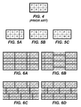
- FIG. 4 (prior art) is a color filter array pattern with both panchromatic and color pixels
- FIGS. 5A-C show several minimal repeating units for color filter array patterns of the present invention
- FIGS. 6A-D show several ways to tile the minimal repeating unit of FIG. 5A ;
- FIGS. 7A-C show several minimal repeating units for color filter array patterns of an alternative embodiment of the present invention employing primary color filters
- FIGS. 8A-D show several ways to tile the minimal repeating unit of FIG. 7A ;
- FIGS. 9A-C show several minimal repeating units for color filter array patterns of an alternative embodiment of the present invention employing complementary color filters
- FIGS. 10A-B show several minimal repeating units for color filter array patterns of an alternative embodiment of the present invention employing panchromatic pixels of different photographic sensitivities;
- FIGS. 11A-C provides alternative minimal repeating units for the color filter arrays of FIGS. 7A-C that results in tiling similar to FIG. 8D ;
- FIG. 12 shows the tiling arrangement for the minimal repeating unit of FIG. 11A ;
- FIGS. 13A-B shows a minimal repeating unit for a color filter array of the present invention in which the pixels are arranged in a octagonal pattern, and includes a tiling arrangement;
- FIG. 14 shows the spatial distribution of color samples from the tiling arrangement of FIG. 8D ;
- FIGS. 15A-B shows a minimal repeating unit for a color filter array of the present invention in which the pixels are arranged in a hexagonal fashion;
- FIG. 16 shows the spatial distribution of color samples from the tiling arrangement of FIG. 15B ;
- FIGS. 17A-E shows the production of lower resolution Bayer images from an image sensor of the present invention
- FIG. 18 is a process diagram of the present invention showing the method of processing the color and panchromatic pixel data from a sensor of the present invention.
- FIG. 19 shows an arrangement of color and panchromatic pixels of the present invention with indices to support the explanation of an interpolation approach.
- FIG. 1 a block diagram of an image capture device shown as a digital camera embodying the present invention is shown.
- a digital camera will now be explained, the present invention is clearly applicable to other types of image capture devices.
- light 10 from the subject scene is input to an imaging stage 11 , where the light is focused by lens 12 to form an image on solid state image sensor 20 .
- Image sensor 20 converts the incident light to an electrical signal for each picture element (pixel).
- the image sensor 20 of the preferred embodiment is a charge coupled device (CCD) type or an active pixel sensor (APS) type (APS devices are often referred to as CMOS sensors because of the ability to fabricate them in a Complementary Metal Oxide Semiconductor Process).
- CCD charge coupled device
- APS active pixel sensor
- FIGS. 4A-D examples of the patterns of color and panchromatic pixels of the present invention that are used with the image sensor 20 are seen in FIGS. 4A-D , FIG. 8A , FIG. 8E , FIGS. 9A-C , FIG. 10A , FIGS. 10C-F , FIGS. 11A-B , FIG. 12 , and FIG. 15 , although other patterns are used within the spirit of the present invention.
- the amount of light reaching the sensor 20 is regulated by an iris block 14 that varies the aperture and the neutral density (ND) filter block 13 that includes one or more ND filters interposed in the optical path. Also regulating the overall light level is the time that the shutter block 18 is open.
- the exposure controller block 40 responds to the amount of light available in the scene as metered by the brightness sensor block 16 and controls all three of these regulating functions.
- the digital camera is a relatively simple point and shoot digital camera, where the shutter 18 is a relatively simple movable blade shutter, or the like, instead of the more complicated focal plane arrangement.
- the present invention can also be practiced on imaging components included in non-camera devices such as mobile phones and automotive vehicles.
- the analog signal from image sensor 20 is processed by analog signal processor 22 and applied to analog to digital (A/D) converter 24 .
- Timing generator 26 produces various clocking signals to select rows and pixels and synchronizes the operation of analog signal processor 22 and A/D converter 24 .
- the image sensor stage 28 includes the image sensor 20 , the analog signal processor 22 , the A/D converter 24 , and the timing generator 26 .
- the components of image sensor stage 28 is separately fabricated integrated circuits, or they are fabricated as a single integrated circuit as is commonly done with CMOS image sensors.
- the resulting stream of digital pixel values from A/D converter 24 is stored in memory 32 associated with digital signal processor (DSP) 36 .
- DSP digital signal processor
- Digital signal processor 36 is one of three processors or controllers in this embodiment, in addition to system controller 50 and exposure controller 40 . Although this partitioning of camera functional control among multiple controllers and processors is typical, these controllers or processors are combined in various ways without affecting the functional operation of the camera and the application of the present invention.
- These controllers or processors can comprise one or more digital signal processor devices, microcontrollers, programmable logic devices, or other digital logic circuits. Although a combination of such controllers or processors has been described, it should be apparent that one controller or processor is designated to perform all of the needed functions. All of these variations can perform the same function and fall within the scope of this invention, and the term “processing stage” will be used as needed to encompass all of this functionality within one phrase, for example, as in processing stage 38 in FIG. 1 .
- DSP 36 manipulates the digital image data in its memory 32 according to a software program permanently stored in program memory 54 and copied to memory 32 for execution during image capture. DSP 36 executes the software necessary for practicing image processing shown in FIG. 18 .
- Memory 32 includes of any type of random access memory, such as SDRAM.
- a bus 30 comprising a pathway for address and data signals connects DSP 36 to its related memory 32 , A/D converter 24 and other related devices.
- System controller 50 controls the overall operation of the camera based on a software program stored in program memory 54 , which can include Flash EEPROM or other nonvolatile memory. This memory can also be used to store image sensor calibration data, user setting selections and other data which must be preserved when the camera is turned off.
- System controller 50 controls the sequence of image capture by directing exposure controller 40 to operate the lens 12 , ND filter 13 , iris 14 , and shutter 18 as previously described, directing the timing generator 26 to operate the image sensor 20 and associated elements, and directing DSP 36 to process the captured image data. After an image is captured and processed, the final image file stored in memory 32 is transferred to a host computer via interface 57 , stored on a removable memory card 64 or other storage device, and displayed for the user on image display 88 .
- a bus 52 includes a pathway for address, data and control signals, and connects system controller 50 to DSP 36 , program memory 54 , system memory 56 , host interface 57 , memory card interface 60 and other related devices.
- Host interface 57 provides a high speed connection to a personal computer (PC) or other host computer for transfer of image data for display, storage, manipulation or printing.
- PC personal computer
- This interface is an IEEE1394 or USB2.0 serial interface or any other suitable digital interface.
- Memory card 64 is typically a Compact Flash (CF) card inserted into socket 62 and connected to the system controller 50 via memory card interface 60 .
- Other types of storage that are used include without limitation PC-Cards, MultiMedia Cards (MMC), or Secure Digital (SD) cards.
- Processed images are copied to a display buffer in system memory 56 and continuously read out via video encoder 80 to produce a video signal.
- This signal is output directly from the camera for display on an external monitor, or processed by display controller 82 and presented on image display 88 .
- This display is typically an active matrix color liquid crystal display (LCD), although other types of displays are used as well.
- a user control and interface status 68 includes all or any combination of viewfinder display 70 , exposure display 72 , status display 76 and image display 88 , and user inputs 74 , is controlled by a combination of software programs executed on exposure controller 40 and system controller 50 .
- User inputs 74 typically include some combination of buttons, rocker switches, joysticks, rotary dials or touchscreens.
- Exposure controller 40 operates light metering, exposure mode, autofocus and other exposure functions.
- the system controller 50 manages the graphical user interface (GUI) presented on one or more of the displays, e.g., on image display 88 .
- the GUI typically includes menus for making various option selections and review modes for examining captured images.
- Exposure controller 40 accepts user inputs selecting exposure mode, lens aperture, exposure time (shutter speed), and exposure index or ISO speed rating and directs the lens and shutter accordingly for subsequent captures.
- Brightness sensor 16 is employed to measure the brightness of the scene and provide an exposure meter function for the user to refer to when manually setting the ISO speed rating, aperture and shutter speed. In this case, as the user changes one or more settings, the light meter indicator presented on viewfinder display 70 tells the user to what degree the image will be over or underexposed.
- an automatic exposure mode the user changes one setting and the exposure controller 40 automatically alters another setting to maintain correct exposure, e.g., for a given ISO speed rating when the user reduces the lens aperture the exposure controller 40 automatically increases the exposure time to maintain the same overall exposure.
- the ISO speed rating is an important attribute of a digital still camera.
- the exposure time, the lens aperture, the lens transmittance, the level and spectral distribution of the scene illumination, and the scene reflectance determine the exposure level of a digital still camera.
- proper tone reproduction can generally be maintained by increasing the electronic or digital gain, but the image will contain an unacceptable amount of noise.
- the gain is decreased, and therefore the image noise can normally be reduced to an acceptable level.
- the resulting signal in bright areas of the image can exceed the maximum signal level capacity of the image sensor or camera signal processing. This can cause image highlights to be clipped to form a uniformly bright area, or to bloom into surrounding areas of the image.
- An ISO speed rating is intended to serve as such a guide.
- the ISO speed rating for a digital still camera should directly relate to the ISO speed rating for photographic film cameras. For example, if a digital still camera has an ISO speed rating of ISO 200, then the same exposure time and aperture should be appropriate for an ISO 200 rated film/process system.
- the ISO speed ratings are intended to harmonize with film ISO speed ratings.
- Digital still cameras can include variable gain, and can provide digital processing after the image data has been captured, enabling tone reproduction to be achieved over a range of camera exposures. It is therefore possible for digital still cameras to have a range of speed ratings. This range is defined as the ISO speed latitude.
- a single value is designated as the inherent ISO speed rating, with the ISO speed latitude upper and lower limits indicating the speed range, that is, a range including effective speed ratings that differ from the inherent ISO speed rating.
- the inherent ISO speed is a numerical value calculated from the exposure provided at the focal plane of a digital still camera to produce specified camera output signal characteristics.
- the inherent speed is usually the exposure index value that produces peak image quality for a given camera system for normal scenes, where the exposure index is a numerical value that is inversely proportional to the exposure provided to the image sensor.
- the image sensor 20 shown in FIG. 1 typically includes a two-dimensional array of light sensitive pixels fabricated on a silicon substrate that provide a way of converting incoming light at each pixel into an electrical signal that is measured. As the sensor is exposed to light, free electrons are generated and captured within the electronic structure at each pixel. Capturing these free electrons for some period of time and then measuring the number of electrons captured or measuring the rate at which free electrons are generated measures the light level at each pixel. In the former case, accumulated charge is shifted out of the array of pixels to a charge to voltage measurement circuit as in a charge coupled device (CCD), or the area close to each pixel contains elements of a charge to voltage measurement circuit as in an active pixel sensor (APS or CMOS sensor).
- CCD charge coupled device
- image sensor 20 Whenever general reference is made to an image sensor in the following description, it is understood to be representative of the image sensor 20 from FIG. 1 . It is further understood that all examples and their equivalents of image sensor architectures and pixel patterns of the present invention disclosed in this specification is used for image sensor 20 .
- a pixel (a contraction of “picture element”) refers to a discrete light sensing area and charge shifting or charge measurement circuitry associated with the light sensing area.
- the term pixel commonly refers to a particular location in the image having associated color values.
- FIG. 2 shows a pattern of red, green, and blue color filters that is commonly used.
- This particular pattern is commonly known as a Bayer color filter array (CFA) after its inventor Bryce Bayer as disclosed in U.S. Pat. No. 3,971,065.
- CFA Bayer color filter array
- This pattern is effectively used in image sensors having a two-dimensional array of color pixels.
- each pixel has a particular color photoresponse that, in this case, is a predominant sensitivity to red, green or blue light.
- Another useful variety of color photoresponses is a predominant sensitivity to magenta, yellow, or cyan light.
- the particular color photoresponse has high sensitivity to certain portions of the visible spectrum, while simultaneously having low sensitivity to other portions of the visible spectrum.
- the term color pixel will refer to a pixel having a color photoresponse.
- the set of color photoresponses selected for use in a sensor usually has three colors, as shown in the Bayer CFA, but it can also include four or more.
- a panchromatic photoresponse refers to a photoresponse having a wider spectral sensitivity than those spectral sensitivities represented in the selected set of color photoresponses.
- a panchromatic photosensitivity can have high sensitivity across the entire visible spectrum.
- panchromatic pixel will refer to a pixel having a panchromatic photoresponse.
- each panchromatic pixel can have an associated filter. Such filter is either a neutral density filter or a color filter.
- each such pattern has a repeating unit that is a contiguous subarray of pixels that acts as a basic building block.
- the entire sensor pattern is produced.
- the juxtaposition of the multiple copies of repeating units is done in diagonal directions as well as in the horizontal and vertical directions.
- a minimal repeating unit is a repeating unit such that no other repeating unit has fewer pixels.
- the CFA in FIG. 2 includes a minimal repeating unit that is two pixels by two pixels as shown by pixel block 100 in FIG. 2 . Multiple copies of this minimal repeating unit are tiled to cover the entire array of pixels in an image sensor.
- the minimal repeating unit is shown with a green pixel in the upper right corner, but three alternative minimal repeating units can easily be discerned by moving the heavy outlined area one pixel to the right, one pixel down, or one pixel diagonally to the right and down.
- pixel block 102 is a repeating unit, it is not a minimal repeating unit because pixel block 100 is a repeating unit and block 100 has fewer pixels than block 102 .
- An image captured using an image sensor having a two-dimensional array with the CFA of FIG. 2 has only one color value at each pixel.
- CFA interpolation techniques are well known in the art and reference is made to the following patents: U.S. Pat. No. 5,506,619, U.S. Pat. No. 5,629,734, and U.S. Pat. No. 5,652,621.
- FIG. 3 shows the relative spectral sensitivities of the pixels with red, green, and blue color filters in a typical camera application.
- the X-axis in FIG. 3 represents light wavelength in nanometers, and the Y-axis represents efficiency.
- curve 110 represents the spectral transmission characteristic of a typical filter used to block infrared and ultraviolet light from reaching the image sensor. Such a filter is needed because the color filters used for image sensors typically do not block infrared light, hence the pixels are unable to distinguish between infrared light and light that is within the passbands of their associated color filters.
- the infrared blocking characteristic shown by curve 110 prevents infrared light from corrupting the visible light signal.
- the spectral quantum efficiency i.e.
- panchromatic photoresponse is three to four times more sensitive to wide spectrum light than any of the color photoresponses.
- another sensor of a different type may have different photoresponses than shown by FIG. 3 , it is clear that the broader panchromatic response will always be more sensitive to wide spectrum light than any of the color photoresponses.
- the greater panchromatic sensitivity shown in FIG. 3 permits improving the overall sensitivity of an image sensor by intermixing pixels that include color filters with pixels that do not include color filters.
- the color filter pixels will be significantly less sensitive than the panchromatic pixels.
- the panchromatic pixels are properly exposed to light such that the range of light intensities from a scene cover the full measurement range of the panchromatic pixels, then the color pixels will be significantly underexposed.
- the sensitivity of the color pixels is increased, for example, by increasing the size of the color pixels relative to the panchromatic pixels, with an associated reduction in spatial pixels.
- panchromatic pixels In an image capture device that includes panchromatic pixels as well as color pixels, the arrangement of panchromatic and color pixels within the pixel array affects the spatial sampling characteristics of the image capture device. To the extent that panchromatic pixels take the place of color pixels, the frequency of color sampling is reduced. For example, if one of the green pixels in minimal repeating unit 100 in FIG. 2 is replaced with a panchromatic pixel, as in Gindele, et al. in U.S. Pat. No. 6,476,865, then the green sampling frequency is reduced because there are half as many green pixels as in the original pattern shown in FIG. 2 . In this particular case, the sampling frequencies of the panchromatic pixels and each of the color pixels are the same.
- panchromatic pixels are generally more sensitive than the color pixels, it is desirable to have higher sampling frequency for the panchromatic pixels than any one of the color pixels, thereby to provide a robust, higher sensitivity panchromatic representation of the image to provide the basis for subsequent image processing and interpolation of missing colors at each pixel.
- Yamagami, et al. in U.S. Pat. No. 5,323,233 shows a pattern with 50% panchromatic pixels, 25% green pixels, and 12.5% each of red and blue pixels. A minimal repeating unit of this pattern is shown in FIG. 4 . Having twice as many green pixels as either of the color pixels is consistent with the widely used Bayer pattern, but it does not necessarily provide an advantage when combined with a robust panchromatic sampling arrangement as shown in Yamagami.
- FIG. 5A shows a minimal repeating unit of the present invention with four panchromatic pixels uniformly disposed throughout the minimal repeating unit, and one red pixel (R), one green pixel (G), one blue pixel (B), and one color pixel having a fourth distinct spectral sensitivity (Q).
- the minimal repeating unit of FIG. 5A takes the additional green pixel of Yamagami ( FIG. 4 ) and replaces it with a pixel having a spectral sensitivity distinct from the other three colors.
- This pattern has 50% panchromatic pixels and 12.5% each of pixels that have one of four distinct spectral sensitivities.
- the Q pixel is a different visible range than provided by R, G, or B; alternatively, the Q pixel encompasses non-visible range.
- the Q pixel can be sensitive to infrared light.
- FIG. 5B shows another minimal repeating unit of the present invention.
- FIG. 5B is similar to FIG. 5A except the green and blue pixels have been exchanged.
- the color sampling frequency for each color remains the same, but the phase relationship between the four color sampling arrangements is different between FIG. 5A and FIG. 5B .
- FIG. 5C shows yet another minimal repeating unit of the present invention.
- FIG. 5C is similar to FIG. 5A except red, green, and blue pixels have been replaced with cyan, yellow, and magenta pixels, respectively, demonstrating that this embodiment of the present invention can be used with any set of four distinct spectral sensitivities.
- FIG. 6A shows a tiling arrangement in which the minimal repeating unit of FIG. 5A is tiled evenly in rows and columns.
- FIG. 6B shows a tiling arrangement for FIG. 5A in which every other column is shifted down (or, equivalently, up) by one pixel; in other words, the minimal repeating unit of FIG. 5A is tiled evenly in columns, with each column shifted vertically by one-half of the minimal repeating unit height with respect to adjacent columns.
- FIG. 6C shows a tiling arrangement in which every row is shifted right by one pixel with respect to the row above; in other words, the minimal repeating unit of FIG.
- FIG. 5A is tiled evenly in rows, with each row shifted right one-quarter of the minimal repeating unit width with respect to the adjacent row above.
- FIG. 6D shows a tiling arrangement in which every other row is shifted right (or, equivalently, left) by two pixels, or one-half of the width of the minimal repeating unit; in other words, the minimal repeating unit of FIG. 5A is tiled evenly in rows, with each row shifted right one-half of the minimal repeating unit width with respect to the adjacent rows.
- FIG. 5A shown in FIGS. 6A through 6C provide pixel arrays with sampling frequencies for the individual colors that are different between the horizontal and vertical directions.
- the tiling arrangement of FIG. 6D provides a pixel array with sampling frequencies for the individual colors that are identical between the horizontal and vertical directions and are identical between the upper-left to lower-right diagonal (slash) and the upper-right to lower left diagonal (backslash) directions; furthermore, the sampling frequencies are identical between colors, and the highest sampling frequency for the colors is associated with the horizontal and vertical directions. Arranging the highest sampling frequency to be associated with the horizontal and vertical directions allows vertical and horizontal edges to be sampled with the lowest chance for aliasing.
- FIG. 6D provides a preferred tiling arrangement for the minimal repeating unit of FIG. 5A .
- Pixels of three different spectral sensitivities are generally sufficient to provide color information for a captured color image.
- the well-known Bayer pattern for example, is commonly implemented with pixels having red, green, and blue sensitivities.
- a panchromatic/color image capture device there is an advantage to providing a greater proportion of panchromatic pixels than any one color pixel in order to capture a robust panchromatic image.
- the pixel with a fourth spectral sensitivity Q in FIG. 5A is made a panchromatic pixel.
- the minimal repeating unit has 62.5% panchromatic pixels and 12.5% each of red, green, and blue pixels. This provides an improved balance between panchromatic sampling to provide a robust panchromatic representation of the image and color sampling to identify colors within the image.
- FIG. 7A shows a minimal repeating unit of an alternative embodiment of the present invention having eight pixels, of which five are panchromatic pixels and the remaining three pixels are three different colors.
- This minimal repeating unit has the proportion of panchromatic pixels and color pixels discussed in the last paragraph.
- the three color pixels are red, green, and blue. Note that several arrangements of three color and five panchromatic pixels are possible.
- FIG. 7B is similar to FIG. 7A except the red and blue pixels are switched, thereby forming a new and distinct minimal repeating unit.
- FIG. 7C is similar to FIG. 7A , except the green and blue pixels are switched.
- FIGS. 8A-8D show tiling arrangements for the minimal repeating unit of FIG. 7A that correspond to the tiling arrangements shown in FIGS. 6A-6D . Based on the discussion regarding FIGS. 6A-6D above, FIG. 8D provides the optimum tiling arrangement for the minimal repeating unit of FIG. 7A .
- FIG. 9A is similar to FIG. 7A except red, green, and blue pixels have been replaced with cyan, yellow, and magenta pixels, respectively, demonstrating that this embodiment of the present invention can be used with any set of three distinct spectral sensitivities for the color pixels.
- FIGS. 9B and 9C show additional arrangements for the cyan, magenta, and yellow color pixels.
- FIG. 10A shows a minimal repeating unit similar to FIG. 5A in which the Q pixel is replaced with a panchromatic pixel of a different photographic speed than the other panchromatic pixels.
- Panchromatic pixels with different photographic sensitivities are used to capture a broader range of light levels.
- FIG. 10B shows another minimal repeating unit with an alternative arrangement of panchromatic pixels with two different photographic speeds, with one row of the minimal repeating unit having one speed and the other row having a different speed.
- FIG. 11A shows a minimal repeating unit of the present invention that is equivalent to the minimal repeating unit of FIG. 7A as tiled in FIG. 8D .
- FIG. 11B is equivalent to FIG. 7B if FIG. 7B is tiled similar to FIG. 8D
- FIG. 11C is equivalent to FIG. 10A if FIG. 10A is tiled similar to FIG. 8D .
- FIG. 13A shows a minimal repeating unit of an arrangement of octagonal pixels that is equivalent to rotating the minimal repeating unit of FIG. 7A forty-five degrees counter-clockwise.
- FIG. 13B shows the minimal repeating unit of FIG. 13A tiled to form a pattern that is equivalent to a forty-five degree counter-clockwise rotation of FIG. 8D .
- each color of the four colors of FIG. 6D or the three colors of FIG. 8D are identical, the phase relationships between the colors are not identical.
- the pixels of each color in FIG. 8D i.e., red, green, and blue
- FIG. 14 which is the same pattern as FIG. 8D with only the color pixels identified.
- each blue pixel is equidistant from four neighboring red pixels, forming a checkerboard of red and blue pixels
- the green pixels are located between red pixels in 45 degree diagonal lines, and between blue pixels in ⁇ 45 degree diagonal lines.
- phase relationship between green and the other two colors is different than between red and blue, even though red, green, and blue individually have identical sampling arrangements. This suggests opportunities for further optimization of a panchromatic/three-color imaging device where the color sampling arrangement is identical for each of the three colors and the phase relationships between the pairs of colors is consistent.
- FIG. 15A shows a minimal repeating unit of yet another embodiment of the present invention.
- the minimal repeating unit of FIG. 15A includes nine pixels, of which six are panchromatic pixels and the remaining three pixels are three different colors.
- This minimal repeating unit represents a pattern that is 2 ⁇ 3 panchromatic pixels, 1/9 red pixels, 1/9 green pixels, and 1/9 blue pixels.
- the three color pixels in FIG. 15A are red, green, and blue, but they could be cyan, magenta, and yellow, or some other set of three colors.
- the panchromatic pixels in FIG. 15A have equal photographic sensitivity, but they could have two or more different sensitivities.
- FIG. 15B shows a tiling arrangement in which the minimal repeating unit of FIG. 15A is tiled evenly in columns, with each column shifted up or down one-half of the minimal repeating unit height with respect to the adjacent columns.
- FIG. 16 shows the pattern of FIG. 15B with only the color pixels identified. It is clear from FIG. 16 that the sampling arrangements for each of the three colors is identical, and the phase relationships between each of the colors is consistent. Where certain of the color pixels in FIG. 14 are closer to certain other colors, all of the color pixels in FIG. 15B are located equidistant from each other.
- DSP 36 provides a processed image from the raw image provided by the sensor and imaging subsystem.
- DSP 36 in many cases provides a hardwired image processing path (as opposed to a programmable image processing path). Such hardwired image processing paths often require sensor data to conform to the Bayer filter pattern:
- FIG. 17A there is shown an arrangement of color and panchromatic pixels of the present invention.
- FIG. 17A is similar to FIG. 8D , with the addition of indices to each pixel to help demonstrate the production of a reduced resolution Bayer image from an image sensor of the present invention.
- FIG. 17A the minimal repeating unit 120 is shown to be the same as that shown in FIG. 7A .
- Let all the green pixels in FIG. 17A e.g., G 12 , G 16 , G 34 , G 38 , etc.
- These green pixels shown circled in FIG. 17B , form the checkerboard of green pixels that are present in the Bayer pattern.
- red and blue pixels in the Bayer pattern combine red and blue pixels in pairs to produce red and blue pixel averages.
- R 21 and R 43 are combined to produce circled red pixel average R′ 32 in FIG. 17B between green pixels G 12 and G 52 .
- Similar diagonal combinations of red pixels provide appropriately positioned red pixel averages in the reduced resolution Bayer image.
- B 45 and B 63 are combined to produce circled blue pixel average B′ 54 in FIG. 17B between green pixels G 34 and G 74 .
- Similar diagonal combinations of blue pixels provide appropriately positioned blue pixel averages in the reduced resolution Bayer image.
- FIG. 17C shows the resulting image: a Bayer image with 1 ⁇ 2 the horizontal resolution and 1 ⁇ 2 the vertical resolution of the original image.
- FIGS. 17A-17C demonstrate the production of a Bayer image that has 1 ⁇ 4 the number of pixels of the original image.
- FIGS. 17D and 17E demonstrate using similar techniques to produce a Bayer image that has 1/16 the number of pixels of the original image.
- Combining pixels as shown in FIG. 17B and FIG. 17 E is done, for example, by combining charge in the pixels, by averaging sampled voltages, or by combining digital representations of the pixel signals.
- the digital signal processor block 36 ( FIG. 1 ) is shown receiving captured raw image data produced by an image sensor of the present invention and carried by the data bus 30 ( FIG. 1 ).
- the raw image data is passed to both the Low-resolution Partial Color block 202 and the High-resolution Panchrome block 204 .
- An example of a minimal repeating unit for an image sensor of the present invention has already been shown in FIG. 7A .
- a partial color image is produced from the captured raw image data, a partial color image being a color image wherein each pixel has at least one color value and each pixel is also missing at least one color value. Since there are proportionately fewer of color pixels with a given spectral response compared to the panchromatic pixels, the partial color image is consequently lower in spatial resolution compared to the image captured by the panchromatic pixels.
- the Low-resolution Partial Color block 202 processes each pixel of the partial color image in a similar manner resulting in an array of color values, one for each low resolution pixel. Although not shown here, it is often advantageous to noise clean the low-resolution partial color image in this step.
- FIG. 19 a filter pattern is shown that is equivalent to the pattern shown in FIG. 17A .
- the minimal repeating unit 220 ( FIG. 19 ) is seen to match the minimal repeating unit 120 ( FIG. 17A ).
- the pixel containing green value G 22 has eight neighboring pan values in the shape of a diamond, namely, P 21 , a, P 12 , b, P 23 , d, P 32 , c.
- clasvert
- classlash
- clasback
- the pan predicted value corresponding to the selected direction produces the interpolated pan value, P 22 .
- pan values have been interpolated for the green pixels, it remains to do the same for the red and blue pixels.
- the same pan interpolation process used for green pixels applies equally well to red and blue pixels.
- the pan pixels P 23 , P 32 , P 34 , and P 43 immediately surround blue pixel B 33 just as pan pixels P 12 , P 21 , P 23 , and P 32 immediately surround green pixel G 22 .
- Neighboring interstitial pan values for pixel B 33 can be computed using equations similar to those given above for green pixel G 22 .
- pan values After pan values have been interpolated at all color pixel positions, there is a pan value, either measured or interpolated, for each pixel position on the sensor. These pan values make up the high resolution panchrome image 204 , as shown in FIG. 19 .
- the low resolution panchrome image 206 is produced by selecting only those pixels having interpolated panchromatic values.
- the low resolution panchrome image 206 is now combined with the low resolution partial color image 202 to produce low resolution color differences 208 .
- the next processing step is to produce the high resolution color differences 210 which begins by finding the green minus pan, G ⁇ P, value for the center pan pixel in each pan diamond. Once a G ⁇ P color difference value is produced, it is then added to the center pan value to produce a green value in the high resolution final image 212 .
- such a center pixel would be P 24 since it is in the center of the diamond shaped collection of pan pixels defined by: P 14 , P 23 , P 24 , P 25 , P 34 .
- the four nearest green values are G 04 , G 22 , G 26 , and G 44 .
- Each of these four green pixels also has an interpolated pan value, so the G ⁇ P color differences can be computed at each location.
- clasvert ( G 04 ⁇ P 04) ⁇ ( G 44 ⁇ P 44)
- the smaller classifier indicates which predictor value to use. The indicated color difference is then added to the pan value at the center pixel, P 24 , to produce the interpolated green value, G 24 .
- the indicated color difference is then added to the pan value at pixel B 33 to produce the interpolated green value, G 33 .
- the same approach is taken for red pixels. Once all these green values have been computed, there are green values for all pixel locations having subscripts that are either both odd or both even.
- the set of equations for interpolating green can be modified and applied to red pixels as well as blue pixels.
- the method of computing a red value involves finding a R ⁇ G color difference value that is then added to an existing green value to produce a red value. Pan values are still used in determining the classifier values.
- the indicated color difference is then added to the green value at the blue pixel, B 24 , to produce the interpolated red value, R 24 .
- a similar set of equations using B ⁇ G color differences can be used to compute blue values at red pixel locations. Once red values have been computed at all blue pixel locations and blue values have been computed at red pixel locations, there are red and blue values for every pixel location having two odd subscripts.
- the next step is to compute red and blue values at pixels having two even subscripts. For example, consider computing a red value at the green pixel location G 44 .
- clasback
- the smaller classifier indicates which predictor value to use.
- the indicated color difference is then added to the green value at pixel G 44 to produce the interpolated red value, R 33 .
- the same approach is taken for blue pixels. Once all the red and blue values have been computed, there are red and blue values for all pixel locations having subscripts that are either both odd or both even.
- the indicated color difference is then added to the green value at the pan pixel location P 32 to produce the interpolated red value, R 32 .
- the same approach, using B-G color differences, is taken to compute the blue value B 32 .
- the color interpolation is done because each pixel has all three color values: red, green, and blue. These pixels make up the high resolution final image 212 .
- PARTS LIST 10 light from subject scene 11 imaging stage 12 lens 13 neutral density filter 14 iris 16 brightness sensor 18 shutter 20 image sensor 22 analog signal processor 24 analog to digital (A/D) converter 26 timing generator 28 image sensor stage 30 digital signal processor (DSP) bus 32 digital signal processor (DSP) memory 36 digital signal processor (DSP) 38 processing stage 40 exposure controller 50 system controller 52 system controller bus 54 program memory 56 system memory 57 host interface 60 memory card interface 62 memory card socket 64 memory card 68 user control and status interface 70 viewfinder display 72 exposure display 74 user inputs 76 status display 80 video encoder 82 display controller 88 image display 100 minimal repeating unit for Bayer pattern 102 repeating unit for Bayer pattern that is not minimal 110 spectral transmission curve of infrared blocking filter 112 unfiltered spectral photoresponse curve of sensor 114 red photoresponse curve of sensor 116 green photoresponse curve of sensor 118 blue photoresponse curve of sensor 120 minimal repeating unit 202 low-resolution partial color block 204 high-resolution
Abstract
Description
| G | R | ||
| B | G | ||
Therefore, it is advantageous to provide the ability to read conveniently a reduced resolution, Bayer image from a sensor of the present invention.
a=(−P30+9*P21+9*P12−P03)/16
b=(−P34+9*P23+9*P12−P01)/16
c=(−P10+9*P21+9*P32−P43)/16
d=(−P14+9*P23+9*P32−P41)/16
Thus, the pixel containing green value G22 has eight neighboring pan values in the shape of a diamond, namely, P21, a, P12, b, P23, d, P32, c. Classifier values can now be computed at pixel G22 using the absolute value of the four center-difference gradients in the horizontal, vertical, slash, and backslash directions:
clashorz=|P23−P21|
clasvert=|P12−P32|
classlash=|b−c|
clasback=|a−d|
The corresponding predictor values for these directions are:
predhorz=(P23+P21)/2
predvert=(P12+P32)/2
predslash=(b+c)/2
predback=(a+d)/2
After selecting the direction having the smallest classifier value, the pan predicted value corresponding to the selected direction produces the interpolated pan value, P22.
clashorz=|(G22−P22)−(G26−P26)|+|P22−2*P24+P26|
clasvert=(G04−P04)−(G44−P44)|+|P04−2*P24+P44|
predhorz=[(G22−P22)+(G26−P26)]/2
predvert=[(G04−P04)+(G44−P44)]/2
The smaller classifier indicates which predictor value to use. The indicated color difference is then added to the pan value at the center pixel, P24, to produce the interpolated green value, G24.
classlash=|(G42−P42)−(G24−P24)|+|P42−2*P33+P24|
clasback=|(G22−P22)−(G44−P44)|+|P22−2*P33+P44|
predslash=[(G42−P42)+(G24−P24)]/2
predback=[(G22−P22)+(G44−P44)]/2
The smaller classifier indicates which predictor value to use. The indicated color difference is then added to the pan value at pixel B33 to produce the interpolated green value, G33. The same approach is taken for red pixels. Once all these green values have been computed, there are green values for all pixel locations having subscripts that are either both odd or both even.
clashorz=|(G31−P31)−(G33−P33)|+|P31−2*P32+P33|
clasvert=|(G22−P22)−(G42−P42)|+|P22−2*P32+P42|
predhorz=[(G31−P31)+(G33−P33)]/2
predvert=[(G22−P22)+(G42−P42)]/2
The smaller classifier indicates which predictor value to use. The indicated color difference is then added to the pan value at the center pixel, P32, to produce the interpolated green value, G32.
clashorz=|(R31−G31)−(R35−G35)|+|P31−2*P33+P35|
clasvert=|(R13−G13)−(R15−G15)|+|P13−2*P33+P15|
predhorz=[(R31−G31)+(R35−G35)]/2
predvert=[(R13−G13)+(R35−G35)]/2
The smaller classifier indicates which predictor value to use. The indicated color difference is then added to the green value at the blue pixel, B24, to produce the interpolated red value, R24. A similar set of equations using B−G color differences can be used to compute blue values at red pixel locations. Once red values have been computed at all blue pixel locations and blue values have been computed at red pixel locations, there are red and blue values for every pixel location having two odd subscripts.
classlash=|(R53−G53)−(R35−G35)|+|P53−2*P44+P35|
clasback=|(R33−G33)−(R55−G55)|+|P33−2*P44+P55|
predslash=[(R53−G53)+(R35−G35)]/2
predback=[(R33−G33)+(R55−G55)]/2
The smaller classifier indicates which predictor value to use. The indicated color difference is then added to the green value at pixel G44 to produce the interpolated red value, R33. The same approach is taken for blue pixels. Once all the red and blue values have been computed, there are red and blue values for all pixel locations having subscripts that are either both odd or both even.
clashorz=|(R31−G31)−(R33−G33)|+|P31−2*P32+P33|
clasvert=|(R22−G22)−(R42−G42)|+|P22−2*P32+P42|
predhorz=[(R31−G31)+(R33−G33)]/2
predvert=[(R22−G22)+(R42−G42)]/2
The smaller classifier indicates which predictor value to use. The indicated color difference is then added to the green value at the pan pixel location P32 to produce the interpolated red value, R32. The same approach, using B-G color differences, is taken to compute the blue value B32. At this point the color interpolation is done because each pixel has all three color values: red, green, and blue. These pixels make up the high resolution
| |
| 10 | light from |
| 11 | |
| 12 | |
| 13 | |
| 14 | |
| 16 | |
| 18 | |
| 20 | |
| 22 | |
| 24 | analog to digital (A/D) |
| 26 | |
| 28 | |
| 30 | digital signal processor (DSP) |
| 32 | digital signal processor (DSP) |
| 36 | digital signal processor (DSP) |
| 38 | |
| 40 | |
| 50 | |
| 52 | |
| 54 | |
| 56 | |
| 57 | |
| 60 | |
| 62 | |
| 64 | |
| 68 | user control and |
| 70 | |
| 72 | |
| 74 | |
| 76 | |
| 80 | |
| 82 | |
| 88 | |
| 100 | minimal repeating unit for |
| 102 | repeating unit for Bayer pattern that is not minimal |
| 110 | spectral transmission curve of |
| 112 | unfiltered spectral photoresponse curve of |
| 114 | red photoresponse curve of |
| 116 | green photoresponse curve of |
| 118 | blue photoresponse curve of |
| 120 | minimal repeating |
| 202 | low-resolution |
| 204 | high-resolution |
| 206 | low-resolution |
| 208 | low-resolution color differences block |
| 210 | high-resolution color differences block |
| 212 | high-resolution |
| 220 | minimal repeating unit of the present invention |
Claims (7)
Priority Applications (6)
| Application Number | Priority Date | Filing Date | Title |
|---|---|---|---|
| US11/565,687 US7893976B2 (en) | 2006-12-01 | 2006-12-01 | Light sensitivity in image sensors |
| EP07840077.7A EP2087725B1 (en) | 2006-12-01 | 2007-11-16 | Improved light sensitivity in image sensors |
| PCT/US2007/024162 WO2008069920A1 (en) | 2006-12-01 | 2007-11-16 | Improved light sensitivity in image sensors |
| JP2009539266A JP5155333B2 (en) | 2006-12-01 | 2007-11-16 | Improved light sensitivity in image sensors |
| TW096145727A TWI435167B (en) | 2006-12-01 | 2007-11-30 | Improved light sensitivity in image sensors |
| JP2012226175A JP5547786B2 (en) | 2006-12-01 | 2012-10-11 | Improved light sensitivity in image sensors |
Applications Claiming Priority (1)
| Application Number | Priority Date | Filing Date | Title |
|---|---|---|---|
| US11/565,687 US7893976B2 (en) | 2006-12-01 | 2006-12-01 | Light sensitivity in image sensors |
Publications (2)
| Publication Number | Publication Date |
|---|---|
| US20080130073A1 US20080130073A1 (en) | 2008-06-05 |
| US7893976B2 true US7893976B2 (en) | 2011-02-22 |
Family
ID=39307035
Family Applications (1)
| Application Number | Title | Priority Date | Filing Date |
|---|---|---|---|
| US11/565,687 Active 2029-12-22 US7893976B2 (en) | 2006-12-01 | 2006-12-01 | Light sensitivity in image sensors |
Country Status (5)
| Country | Link |
|---|---|
| US (1) | US7893976B2 (en) |
| EP (1) | EP2087725B1 (en) |
| JP (2) | JP5155333B2 (en) |
| TW (1) | TWI435167B (en) |
| WO (1) | WO2008069920A1 (en) |
Cited By (18)
| Publication number | Priority date | Publication date | Assignee | Title |
|---|---|---|---|---|
| US20070024879A1 (en) * | 2005-07-28 | 2007-02-01 | Eastman Kodak Company | Processing color and panchromatic pixels |
| US20100232692A1 (en) * | 2009-03-10 | 2010-09-16 | Mrityunjay Kumar | Cfa image with synthetic panchromatic image |
| US20100245636A1 (en) * | 2009-03-27 | 2010-09-30 | Mrityunjay Kumar | Producing full-color image using cfa image |
| US20100265370A1 (en) * | 2009-04-15 | 2010-10-21 | Mrityunjay Kumar | Producing full-color image with reduced motion blur |
| US20100302423A1 (en) * | 2009-05-27 | 2010-12-02 | Adams Jr James E | Four-channel color filter array pattern |
| US20100302418A1 (en) * | 2009-05-28 | 2010-12-02 | Adams Jr James E | Four-channel color filter array interpolation |
| US20100309350A1 (en) * | 2009-06-05 | 2010-12-09 | Adams Jr James E | Color filter array pattern having four-channels |
| US20100309347A1 (en) * | 2009-06-09 | 2010-12-09 | Adams Jr James E | Interpolation for four-channel color filter array |
| US20110115957A1 (en) * | 2008-07-09 | 2011-05-19 | Brady Frederick T | Backside illuminated image sensor with reduced dark current |
| US20110115954A1 (en) * | 2009-11-19 | 2011-05-19 | Eastman Kodak Company | Sparse color pixel array with pixel substitutes |
| US20110211109A1 (en) * | 2006-05-22 | 2011-09-01 | Compton John T | Image sensor with improved light sensitivity |
| US8119435B2 (en) | 2008-07-09 | 2012-02-21 | Omnivision Technologies, Inc. | Wafer level processing for backside illuminated image sensors |
| US8139130B2 (en) | 2005-07-28 | 2012-03-20 | Omnivision Technologies, Inc. | Image sensor with improved light sensitivity |
| US8416339B2 (en) | 2006-10-04 | 2013-04-09 | Omni Vision Technologies, Inc. | Providing multiple video signals from single sensor |
| US9369681B1 (en) | 2014-11-25 | 2016-06-14 | Omnivision Technologies, Inc. | RGBC color filter array patterns to minimize color aliasing |
| US9667933B2 (en) | 2013-07-01 | 2017-05-30 | Omnivision Technologies, Inc. | Color and infrared filter array patterns to reduce color aliasing |
| US9692992B2 (en) | 2013-07-01 | 2017-06-27 | Omnivision Technologies, Inc. | Color and infrared filter array patterns to reduce color aliasing |
| US11470286B2 (en) * | 2019-07-16 | 2022-10-11 | Mritunjay Singh | Image sensors with color, panchromatic and infrared pixels |
Families Citing this family (26)
| Publication number | Priority date | Publication date | Assignee | Title |
|---|---|---|---|---|
| US8594451B2 (en) * | 2007-03-30 | 2013-11-26 | Omnivision Technologies, Inc. | Edge mapping incorporating panchromatic pixels |
| US7844127B2 (en) * | 2007-03-30 | 2010-11-30 | Eastman Kodak Company | Edge mapping using panchromatic pixels |
| JP5250315B2 (en) * | 2007-06-28 | 2013-07-31 | 富士フイルム株式会社 | Signal processing device, imaging device, and synchronization processing program |
| DE102008027188A1 (en) * | 2008-06-06 | 2009-12-10 | Volkswagen Ag | Image acquisition unit for detecting e.g. color information, has light sensors that act as intensity and color sensors, where number of intensity sensors is greater than number of color sensors |
| US7948534B2 (en) * | 2008-10-22 | 2011-05-24 | Eastman Kodak Company | Charge-coupled device image sensor with vertical binning of same-color pixels |
| US8073246B2 (en) * | 2008-11-07 | 2011-12-06 | Omnivision Technologies, Inc. | Modifying color and panchromatic channel CFA image |
| JP4683121B2 (en) * | 2008-12-08 | 2011-05-11 | ソニー株式会社 | Solid-state imaging device, signal processing method for solid-state imaging device, and imaging device |
| JP4626706B2 (en) * | 2008-12-08 | 2011-02-09 | ソニー株式会社 | Solid-state imaging device, signal processing method for solid-state imaging device, and imaging device |
| TWI422020B (en) * | 2008-12-08 | 2014-01-01 | Sony Corp | Solid-state imaging device |
| EP2380038B1 (en) | 2008-12-22 | 2019-01-09 | Koninklijke Philips N.V. | Cmos imager |
| US8198578B2 (en) * | 2009-06-23 | 2012-06-12 | Nokia Corporation | Color filters for sub-diffraction limit-sized light sensors |
| JP2011199452A (en) * | 2010-03-18 | 2011-10-06 | Fuji Xerox Co Ltd | Processor and control program |
| JP5757711B2 (en) * | 2010-09-27 | 2015-07-29 | オリンパス株式会社 | Spectral information measurement method, color sensor, and virtual slide device |
| JP6035744B2 (en) * | 2012-01-10 | 2016-11-30 | 凸版印刷株式会社 | Solid-state image sensor |
| DE102012021736B4 (en) | 2012-03-22 | 2021-08-05 | Volkswagen Aktiengesellschaft | Image sensor for visible and infrared light and camera system |
| RU2014138087A (en) * | 2012-03-27 | 2016-04-10 | Сони Корпорейшн | IMAGE PROCESSING DEVICE, IMAGE FORMING DEVICE, IMAGE PROCESSING METHOD AND PROGRAM |
| EP2677732B1 (en) | 2012-06-22 | 2019-08-28 | Nokia Technologies Oy | Method, apparatus and computer program product for capturing video content |
| DE102012110092A1 (en) * | 2012-10-23 | 2014-04-24 | Conti Temic Microelectronic Gmbh | Sensor arrangement for image acquisition |
| CN103051849B (en) * | 2012-12-18 | 2017-09-29 | 上海集成电路研发中心有限公司 | The pel array of new structure |
| US9883149B2 (en) | 2014-08-01 | 2018-01-30 | Sri International | Imaging sensor and method for color night vision |
| US9998695B2 (en) * | 2016-01-29 | 2018-06-12 | Ford Global Technologies, Llc | Automotive imaging system including an electronic image sensor having a sparse color filter array |
| JP6311771B2 (en) * | 2016-10-31 | 2018-04-18 | 凸版印刷株式会社 | Solid-state image sensor |
| JP7281895B2 (en) * | 2018-12-06 | 2023-05-26 | ソニーセミコンダクタソリューションズ株式会社 | Image sensor and electronic equipment |
| KR20200108953A (en) * | 2019-03-11 | 2020-09-22 | 삼성전자주식회사 | Rgbw image sensor, binning method in image sensor and computer readable medium for performing the method |
| CN111447380B (en) * | 2020-05-22 | 2022-03-22 | Oppo广东移动通信有限公司 | Control method, camera assembly and mobile terminal |
| CN112702490A (en) * | 2020-12-25 | 2021-04-23 | Oppo广东移动通信有限公司 | Control method of electronic device, and storage medium |
Citations (13)
| Publication number | Priority date | Publication date | Assignee | Title |
|---|---|---|---|---|
| US4390895A (en) | 1980-10-07 | 1983-06-28 | Tokyo Shibaura Denki Kabushiki Kaisha | Color image pick-up apparatus |
| US4437112A (en) | 1980-02-15 | 1984-03-13 | Canon Kabushiki Kaisha | Solid-state color imaging apparatus |
| US4760441A (en) | 1983-11-10 | 1988-07-26 | Nec Corporation | Solid-state color imaging apparatus having color filter array which eliminates vertical color error |
| US4823186A (en) | 1986-12-19 | 1989-04-18 | Fuji Photo Film Co., Ltd. | Color video signal generating device using monochrome and color image sensors having different resolutions to form a luminance signal |
| US4939573A (en) * | 1983-03-17 | 1990-07-03 | Nec Corporation | Color filter arrangement comprising transparent or white filters for solid state color imaging apparatus |
| US5323233A (en) | 1990-07-31 | 1994-06-21 | Canon Kabushiki Kaisha | Image signal processing apparatus having a color filter with offset luminance filter elements |
| US6326624B1 (en) | 1996-11-08 | 2001-12-04 | Commissariat A L'energie Atomique | Device and method for determining the assumed position of a phenomenon relative to a set of photodetectors, and application to gamma-cameras |
| US6476865B1 (en) | 2001-03-07 | 2002-11-05 | Eastman Kodak Company | Sparsely sampled image sensing device with color and luminance photosites |
| US20030210332A1 (en) | 2002-05-08 | 2003-11-13 | Frame Wayne W. | One chip, low light level color camera |
| US6876384B1 (en) * | 2000-04-19 | 2005-04-05 | Biomorphic Vlsi, Inc. | Pixel selective white balancing |
| US20060119738A1 (en) * | 2004-12-07 | 2006-06-08 | Konica Minolta Photo Imaging, Inc. | Image sensor, image capturing apparatus, and image processing method |
| US20070076269A1 (en) * | 2005-10-03 | 2007-04-05 | Konica Minolta Photo Imaging, Inc. | Imaging unit and image sensor |
| US20070177236A1 (en) | 2006-01-27 | 2007-08-02 | Eastman Kodak Company | Image sensor with improved light sensitivity |
Family Cites Families (6)
| Publication number | Priority date | Publication date | Assignee | Title |
|---|---|---|---|---|
| JPS5986982A (en) * | 1982-11-11 | 1984-05-19 | Shoichi Tanaka | Solid-state image pickup device |
| JPS6238692A (en) * | 1985-08-13 | 1987-02-19 | Mitsubishi Electric Corp | Color solid-state image pickup element |
| JPH0823542A (en) * | 1994-07-11 | 1996-01-23 | Canon Inc | Image pickup device |
| US6765611B1 (en) * | 2000-11-21 | 2004-07-20 | Eastman Kodak Company | Method for compressing an image from a sparsely sampled extended dynamic range image sensing device |
| EP1594321A3 (en) * | 2004-05-07 | 2006-01-25 | Dialog Semiconductor GmbH | Extended dynamic range in color imagers |
| JP5183880B2 (en) * | 2006-03-14 | 2013-04-17 | ソニー株式会社 | Color filter and image sensor |
-
2006
- 2006-12-01 US US11/565,687 patent/US7893976B2/en active Active
-
2007
- 2007-11-16 EP EP07840077.7A patent/EP2087725B1/en active Active
- 2007-11-16 JP JP2009539266A patent/JP5155333B2/en active Active
- 2007-11-16 WO PCT/US2007/024162 patent/WO2008069920A1/en active Application Filing
- 2007-11-30 TW TW096145727A patent/TWI435167B/en active
-
2012
- 2012-10-11 JP JP2012226175A patent/JP5547786B2/en active Active
Patent Citations (14)
| Publication number | Priority date | Publication date | Assignee | Title |
|---|---|---|---|---|
| US4437112A (en) | 1980-02-15 | 1984-03-13 | Canon Kabushiki Kaisha | Solid-state color imaging apparatus |
| US4567510A (en) * | 1980-02-15 | 1986-01-28 | Canon Kabushiki Kaisha | Solid state color imaging apparatus |
| US4390895A (en) | 1980-10-07 | 1983-06-28 | Tokyo Shibaura Denki Kabushiki Kaisha | Color image pick-up apparatus |
| US4939573A (en) * | 1983-03-17 | 1990-07-03 | Nec Corporation | Color filter arrangement comprising transparent or white filters for solid state color imaging apparatus |
| US4760441A (en) | 1983-11-10 | 1988-07-26 | Nec Corporation | Solid-state color imaging apparatus having color filter array which eliminates vertical color error |
| US4823186A (en) | 1986-12-19 | 1989-04-18 | Fuji Photo Film Co., Ltd. | Color video signal generating device using monochrome and color image sensors having different resolutions to form a luminance signal |
| US5323233A (en) | 1990-07-31 | 1994-06-21 | Canon Kabushiki Kaisha | Image signal processing apparatus having a color filter with offset luminance filter elements |
| US6326624B1 (en) | 1996-11-08 | 2001-12-04 | Commissariat A L'energie Atomique | Device and method for determining the assumed position of a phenomenon relative to a set of photodetectors, and application to gamma-cameras |
| US6876384B1 (en) * | 2000-04-19 | 2005-04-05 | Biomorphic Vlsi, Inc. | Pixel selective white balancing |
| US6476865B1 (en) | 2001-03-07 | 2002-11-05 | Eastman Kodak Company | Sparsely sampled image sensing device with color and luminance photosites |
| US20030210332A1 (en) | 2002-05-08 | 2003-11-13 | Frame Wayne W. | One chip, low light level color camera |
| US20060119738A1 (en) * | 2004-12-07 | 2006-06-08 | Konica Minolta Photo Imaging, Inc. | Image sensor, image capturing apparatus, and image processing method |
| US20070076269A1 (en) * | 2005-10-03 | 2007-04-05 | Konica Minolta Photo Imaging, Inc. | Imaging unit and image sensor |
| US20070177236A1 (en) | 2006-01-27 | 2007-08-02 | Eastman Kodak Company | Image sensor with improved light sensitivity |
Cited By (30)
| Publication number | Priority date | Publication date | Assignee | Title |
|---|---|---|---|---|
| US8711452B2 (en) | 2005-07-28 | 2014-04-29 | Omnivision Technologies, Inc. | Processing color and panchromatic pixels |
| US8139130B2 (en) | 2005-07-28 | 2012-03-20 | Omnivision Technologies, Inc. | Image sensor with improved light sensitivity |
| US20070024879A1 (en) * | 2005-07-28 | 2007-02-01 | Eastman Kodak Company | Processing color and panchromatic pixels |
| US8274715B2 (en) | 2005-07-28 | 2012-09-25 | Omnivision Technologies, Inc. | Processing color and panchromatic pixels |
| US8330839B2 (en) | 2005-07-28 | 2012-12-11 | Omnivision Technologies, Inc. | Image sensor with improved light sensitivity |
| US20110211109A1 (en) * | 2006-05-22 | 2011-09-01 | Compton John T | Image sensor with improved light sensitivity |
| US8194296B2 (en) | 2006-05-22 | 2012-06-05 | Omnivision Technologies, Inc. | Image sensor with improved light sensitivity |
| US8416339B2 (en) | 2006-10-04 | 2013-04-09 | Omni Vision Technologies, Inc. | Providing multiple video signals from single sensor |
| US8119435B2 (en) | 2008-07-09 | 2012-02-21 | Omnivision Technologies, Inc. | Wafer level processing for backside illuminated image sensors |
| US20110115957A1 (en) * | 2008-07-09 | 2011-05-19 | Brady Frederick T | Backside illuminated image sensor with reduced dark current |
| US8224082B2 (en) | 2009-03-10 | 2012-07-17 | Omnivision Technologies, Inc. | CFA image with synthetic panchromatic image |
| US20100232692A1 (en) * | 2009-03-10 | 2010-09-16 | Mrityunjay Kumar | Cfa image with synthetic panchromatic image |
| US8068153B2 (en) | 2009-03-27 | 2011-11-29 | Omnivision Technologies, Inc. | Producing full-color image using CFA image |
| US20100245636A1 (en) * | 2009-03-27 | 2010-09-30 | Mrityunjay Kumar | Producing full-color image using cfa image |
| US8045024B2 (en) | 2009-04-15 | 2011-10-25 | Omnivision Technologies, Inc. | Producing full-color image with reduced motion blur |
| US20100265370A1 (en) * | 2009-04-15 | 2010-10-21 | Mrityunjay Kumar | Producing full-color image with reduced motion blur |
| US8203633B2 (en) | 2009-05-27 | 2012-06-19 | Omnivision Technologies, Inc. | Four-channel color filter array pattern |
| US20100302423A1 (en) * | 2009-05-27 | 2010-12-02 | Adams Jr James E | Four-channel color filter array pattern |
| US20100302418A1 (en) * | 2009-05-28 | 2010-12-02 | Adams Jr James E | Four-channel color filter array interpolation |
| US8237831B2 (en) | 2009-05-28 | 2012-08-07 | Omnivision Technologies, Inc. | Four-channel color filter array interpolation |
| US8125546B2 (en) * | 2009-06-05 | 2012-02-28 | Omnivision Technologies, Inc. | Color filter array pattern having four-channels |
| US20100309350A1 (en) * | 2009-06-05 | 2010-12-09 | Adams Jr James E | Color filter array pattern having four-channels |
| US8253832B2 (en) | 2009-06-09 | 2012-08-28 | Omnivision Technologies, Inc. | Interpolation for four-channel color filter array |
| US20100309347A1 (en) * | 2009-06-09 | 2010-12-09 | Adams Jr James E | Interpolation for four-channel color filter array |
| US20110115954A1 (en) * | 2009-11-19 | 2011-05-19 | Eastman Kodak Company | Sparse color pixel array with pixel substitutes |
| US9667933B2 (en) | 2013-07-01 | 2017-05-30 | Omnivision Technologies, Inc. | Color and infrared filter array patterns to reduce color aliasing |
| US9692992B2 (en) | 2013-07-01 | 2017-06-27 | Omnivision Technologies, Inc. | Color and infrared filter array patterns to reduce color aliasing |
| US9369681B1 (en) | 2014-11-25 | 2016-06-14 | Omnivision Technologies, Inc. | RGBC color filter array patterns to minimize color aliasing |
| US9521381B2 (en) | 2014-11-25 | 2016-12-13 | Omnivision Technologies, Inc. | RGBC color filter array patterns to minimize color aliasing |
| US11470286B2 (en) * | 2019-07-16 | 2022-10-11 | Mritunjay Singh | Image sensors with color, panchromatic and infrared pixels |
Also Published As
| Publication number | Publication date |
|---|---|
| TW200834227A (en) | 2008-08-16 |
| JP2013042530A (en) | 2013-02-28 |
| EP2087725A1 (en) | 2009-08-12 |
| EP2087725B1 (en) | 2018-10-10 |
| US20080130073A1 (en) | 2008-06-05 |
| JP5547786B2 (en) | 2014-07-16 |
| JP2010512050A (en) | 2010-04-15 |
| WO2008069920A1 (en) | 2008-06-12 |
| TWI435167B (en) | 2014-04-21 |
| JP5155333B2 (en) | 2013-03-06 |
Similar Documents
| Publication | Publication Date | Title |
|---|---|---|
| US7893976B2 (en) | Light sensitivity in image sensors | |
| USRE47458E1 (en) | Pattern conversion for interpolation | |
| US7688368B2 (en) | Image sensor with improved light sensitivity | |
| US8139130B2 (en) | Image sensor with improved light sensitivity | |
| US8711452B2 (en) | Processing color and panchromatic pixels | |
| US8237831B2 (en) | Four-channel color filter array interpolation | |
| US8203633B2 (en) | Four-channel color filter array pattern | |
| US20090051984A1 (en) | Image sensor having checkerboard pattern | |
| US8125546B2 (en) | Color filter array pattern having four-channels | |
| JP5345944B2 (en) | Low resolution image generation | |
| US8253832B2 (en) | Interpolation for four-channel color filter array | |
| US7916362B2 (en) | Image sensor with improved light sensitivity | |
| US20110115954A1 (en) | Sparse color pixel array with pixel substitutes |
Legal Events
| Date | Code | Title | Description |
|---|---|---|---|
| AS | Assignment |
Owner name: EASTMAN KODAK COMPANY, NEW YORK Free format text: ASSIGNMENT OF ASSIGNORS INTEREST;ASSIGNORS:COMPTON, JOHN T.;O'BRIEN, MICHELE;HAMILTON, JOHN F., JR.;REEL/FRAME:018570/0556 Effective date: 20061130 |
|
| FEPP | Fee payment procedure |
Free format text: PAYOR NUMBER ASSIGNED (ORIGINAL EVENT CODE: ASPN); ENTITY STATUS OF PATENT OWNER: LARGE ENTITY |
|
| STCF | Information on status: patent grant |
Free format text: PATENTED CASE |
|
| AS | Assignment |
Owner name: OMNIVISION TECHNOLOGIES, INC., CALIFORNIA Free format text: ASSIGNMENT OF ASSIGNORS INTEREST;ASSIGNOR:EASTMAN KODAK COMPANY;REEL/FRAME:026227/0213 Effective date: 20110415 |
|
| FEPP | Fee payment procedure |
Free format text: PAYER NUMBER DE-ASSIGNED (ORIGINAL EVENT CODE: RMPN); ENTITY STATUS OF PATENT OWNER: LARGE ENTITY Free format text: PAYOR NUMBER ASSIGNED (ORIGINAL EVENT CODE: ASPN); ENTITY STATUS OF PATENT OWNER: LARGE ENTITY |
|
| FPAY | Fee payment |
Year of fee payment: 4 |
|
| MAFP | Maintenance fee payment |
Free format text: PAYMENT OF MAINTENANCE FEE, 8TH YEAR, LARGE ENTITY (ORIGINAL EVENT CODE: M1552) Year of fee payment: 8 |
|
| MAFP | Maintenance fee payment |
Free format text: PAYMENT OF MAINTENANCE FEE, 12TH YEAR, LARGE ENTITY (ORIGINAL EVENT CODE: M1553); ENTITY STATUS OF PATENT OWNER: LARGE ENTITY Year of fee payment: 12 |