EP1760127A2 - Polierverfahren - Google Patents
Polierverfahren Download PDFInfo
- Publication number
- EP1760127A2 EP1760127A2 EP06020541A EP06020541A EP1760127A2 EP 1760127 A2 EP1760127 A2 EP 1760127A2 EP 06020541 A EP06020541 A EP 06020541A EP 06020541 A EP06020541 A EP 06020541A EP 1760127 A2 EP1760127 A2 EP 1760127A2
- Authority
- EP
- European Patent Office
- Prior art keywords
- polishing
- metal film
- solution
- abrasive
- cmp
- Prior art date
- Legal status (The legal status is an assumption and is not a legal conclusion. Google has not performed a legal analysis and makes no representation as to the accuracy of the status listed.)
- Withdrawn
Links
- 238000005498 polishing Methods 0.000 title claims abstract description 356
- 238000000034 method Methods 0.000 title claims abstract description 93
- 229910052751 metal Inorganic materials 0.000 claims abstract description 107
- 239000002184 metal Substances 0.000 claims abstract description 107
- 238000004140 cleaning Methods 0.000 claims abstract description 45
- 239000000126 substance Substances 0.000 claims abstract description 32
- 239000007800 oxidant agent Substances 0.000 claims abstract description 21
- 239000010949 copper Substances 0.000 claims description 79
- KRKNYBCHXYNGOX-UHFFFAOYSA-N citric acid Chemical compound OC(=O)CC(O)(C(O)=O)CC(O)=O KRKNYBCHXYNGOX-UHFFFAOYSA-N 0.000 claims description 75
- 229910052802 copper Inorganic materials 0.000 claims description 75
- RYGMFSIKBFXOCR-UHFFFAOYSA-N Copper Chemical compound [Cu] RYGMFSIKBFXOCR-UHFFFAOYSA-N 0.000 claims description 72
- MHAJPDPJQMAIIY-UHFFFAOYSA-N Hydrogen peroxide Chemical group OO MHAJPDPJQMAIIY-UHFFFAOYSA-N 0.000 claims description 70
- 238000005530 etching Methods 0.000 claims description 52
- PNEYBMLMFCGWSK-UHFFFAOYSA-N aluminium oxide Inorganic materials [O-2].[O-2].[O-2].[Al+3].[Al+3] PNEYBMLMFCGWSK-UHFFFAOYSA-N 0.000 claims description 41
- 230000007797 corrosion Effects 0.000 claims description 37
- 238000005260 corrosion Methods 0.000 claims description 37
- 239000000758 substrate Substances 0.000 claims description 33
- 239000003112 inhibitor Substances 0.000 claims description 26
- 239000004065 semiconductor Substances 0.000 claims description 21
- 230000033116 oxidation-reduction process Effects 0.000 claims description 14
- 229910052721 tungsten Inorganic materials 0.000 claims description 14
- WFKWXMTUELFFGS-UHFFFAOYSA-N tungsten Chemical compound [W] WFKWXMTUELFFGS-UHFFFAOYSA-N 0.000 claims description 13
- 239000010937 tungsten Substances 0.000 claims description 13
- 239000002253 acid Substances 0.000 claims description 12
- 238000004519 manufacturing process Methods 0.000 claims description 12
- 230000020477 pH reduction Effects 0.000 claims description 12
- BJEPYKJPYRNKOW-REOHCLBHSA-N (S)-malic acid Chemical compound OC(=O)[C@@H](O)CC(O)=O BJEPYKJPYRNKOW-REOHCLBHSA-N 0.000 claims description 10
- GRYLNZFGIOXLOG-UHFFFAOYSA-N Nitric acid Chemical compound O[N+]([O-])=O GRYLNZFGIOXLOG-UHFFFAOYSA-N 0.000 claims description 10
- BJEPYKJPYRNKOW-UHFFFAOYSA-N alpha-hydroxysuccinic acid Natural products OC(=O)C(O)CC(O)=O BJEPYKJPYRNKOW-UHFFFAOYSA-N 0.000 claims description 10
- 239000001630 malic acid Substances 0.000 claims description 10
- 235000011090 malic acid Nutrition 0.000 claims description 10
- 229910017604 nitric acid Inorganic materials 0.000 claims description 10
- VCJMYUPGQJHHFU-UHFFFAOYSA-N iron(3+);trinitrate Chemical compound [Fe+3].[O-][N+]([O-])=O.[O-][N+]([O-])=O.[O-][N+]([O-])=O VCJMYUPGQJHHFU-UHFFFAOYSA-N 0.000 claims description 9
- VHUUQVKOLVNVRT-UHFFFAOYSA-N Ammonium hydroxide Chemical compound [NH4+].[OH-] VHUUQVKOLVNVRT-UHFFFAOYSA-N 0.000 claims description 8
- 229910000881 Cu alloy Inorganic materials 0.000 claims description 8
- 239000012964 benzotriazole Substances 0.000 claims description 8
- NLXLAEXVIDQMFP-UHFFFAOYSA-N Ammonia chloride Chemical compound [NH4+].[Cl-] NLXLAEXVIDQMFP-UHFFFAOYSA-N 0.000 claims description 7
- 239000000908 ammonium hydroxide Substances 0.000 claims description 7
- 238000001035 drying Methods 0.000 claims description 7
- 150000007524 organic acids Chemical class 0.000 claims description 7
- 238000001514 detection method Methods 0.000 claims description 6
- 230000003287 optical effect Effects 0.000 claims description 6
- 150000003839 salts Chemical class 0.000 claims description 6
- 125000003354 benzotriazolyl group Chemical group N1N=NC2=C1C=CC=C2* 0.000 claims description 5
- 238000001228 spectrum Methods 0.000 claims description 5
- 239000004094 surface-active agent Substances 0.000 claims description 5
- 238000007517 polishing process Methods 0.000 claims description 4
- JLKDVMWYMMLWTI-UHFFFAOYSA-M potassium iodate Chemical compound [K+].[O-]I(=O)=O JLKDVMWYMMLWTI-UHFFFAOYSA-M 0.000 claims description 4
- 239000001230 potassium iodate Substances 0.000 claims description 4
- 229940093930 potassium iodate Drugs 0.000 claims description 4
- 235000006666 potassium iodate Nutrition 0.000 claims description 4
- 239000010936 titanium Substances 0.000 claims description 4
- 229910052719 titanium Inorganic materials 0.000 claims description 4
- PAWQVTBBRAZDMG-UHFFFAOYSA-N 2-(3-bromo-2-fluorophenyl)acetic acid Chemical compound OC(=O)CC1=CC=CC(Br)=C1F PAWQVTBBRAZDMG-UHFFFAOYSA-N 0.000 claims description 3
- RTAQQCXQSZGOHL-UHFFFAOYSA-N Titanium Chemical compound [Ti] RTAQQCXQSZGOHL-UHFFFAOYSA-N 0.000 claims description 3
- NRTOMJZYCJJWKI-UHFFFAOYSA-N Titanium nitride Chemical compound [Ti]#N NRTOMJZYCJJWKI-UHFFFAOYSA-N 0.000 claims description 3
- 235000019270 ammonium chloride Nutrition 0.000 claims description 3
- 229910001069 Ti alloy Inorganic materials 0.000 claims description 2
- 229910001080 W alloy Inorganic materials 0.000 claims description 2
- 230000008859 change Effects 0.000 claims description 2
- QRUDEWIWKLJBPS-UHFFFAOYSA-N benzotriazole Chemical compound C1=CC=C2N[N][N]C2=C1 QRUDEWIWKLJBPS-UHFFFAOYSA-N 0.000 claims 3
- 150000003609 titanium compounds Chemical class 0.000 claims 2
- 239000005749 Copper compound Substances 0.000 claims 1
- 150000003868 ammonium compounds Chemical class 0.000 claims 1
- 150000001880 copper compounds Chemical class 0.000 claims 1
- 150000003658 tungsten compounds Chemical class 0.000 claims 1
- 230000003628 erosive effect Effects 0.000 abstract description 27
- 239000002002 slurry Substances 0.000 abstract description 25
- 230000002829 reductive effect Effects 0.000 abstract description 21
- 230000008569 process Effects 0.000 abstract description 18
- 238000012545 processing Methods 0.000 abstract description 8
- 239000000243 solution Substances 0.000 description 166
- 239000010408 film Substances 0.000 description 79
- 239000010410 layer Substances 0.000 description 57
- VYPSYNLAJGMNEJ-UHFFFAOYSA-N Silicium dioxide Chemical compound O=[Si]=O VYPSYNLAJGMNEJ-UHFFFAOYSA-N 0.000 description 42
- 235000012431 wafers Nutrition 0.000 description 35
- 238000010586 diagram Methods 0.000 description 31
- 239000000377 silicon dioxide Substances 0.000 description 21
- DHMQDGOQFOQNFH-UHFFFAOYSA-N Glycine Chemical compound NCC(O)=O DHMQDGOQFOQNFH-UHFFFAOYSA-N 0.000 description 18
- 235000012239 silicon dioxide Nutrition 0.000 description 18
- XLYOFNOQVPJJNP-UHFFFAOYSA-N water Substances O XLYOFNOQVPJJNP-UHFFFAOYSA-N 0.000 description 17
- ATJFFYVFTNAWJD-UHFFFAOYSA-N Tin Chemical compound [Sn] ATJFFYVFTNAWJD-UHFFFAOYSA-N 0.000 description 14
- 229910052718 tin Inorganic materials 0.000 description 14
- 230000000694 effects Effects 0.000 description 12
- OFOBLEOULBTSOW-UHFFFAOYSA-N Malonic acid Chemical compound OC(=O)CC(O)=O OFOBLEOULBTSOW-UHFFFAOYSA-N 0.000 description 9
- 229960002449 glycine Drugs 0.000 description 9
- 235000013905 glycine and its sodium salt Nutrition 0.000 description 9
- 239000003153 chemical reaction reagent Substances 0.000 description 8
- 239000002245 particle Substances 0.000 description 8
- XNGIFLGASWRNHJ-UHFFFAOYSA-N phthalic acid Chemical compound OC(=O)C1=CC=CC=C1C(O)=O XNGIFLGASWRNHJ-UHFFFAOYSA-N 0.000 description 8
- 230000009467 reduction Effects 0.000 description 8
- 235000011114 ammonium hydroxide Nutrition 0.000 description 7
- 230000003247 decreasing effect Effects 0.000 description 7
- 230000007547 defect Effects 0.000 description 7
- 239000000463 material Substances 0.000 description 7
- 238000007254 oxidation reaction Methods 0.000 description 7
- 238000012360 testing method Methods 0.000 description 7
- KWYUFKZDYYNOTN-UHFFFAOYSA-M Potassium hydroxide Chemical compound [OH-].[K+] KWYUFKZDYYNOTN-UHFFFAOYSA-M 0.000 description 6
- KDYFGRWQOYBRFD-UHFFFAOYSA-N Succinic acid Natural products OC(=O)CCC(O)=O KDYFGRWQOYBRFD-UHFFFAOYSA-N 0.000 description 6
- 239000007864 aqueous solution Substances 0.000 description 6
- 230000007423 decrease Effects 0.000 description 6
- 230000001590 oxidative effect Effects 0.000 description 6
- 239000007787 solid Substances 0.000 description 6
- -1 Cu2+ ion Chemical class 0.000 description 5
- KRHYYFGTRYWZRS-UHFFFAOYSA-N Fluorane Chemical compound F KRHYYFGTRYWZRS-UHFFFAOYSA-N 0.000 description 5
- XUIMIQQOPSSXEZ-UHFFFAOYSA-N Silicon Chemical compound [Si] XUIMIQQOPSSXEZ-UHFFFAOYSA-N 0.000 description 5
- 238000006243 chemical reaction Methods 0.000 description 5
- 239000000428 dust Substances 0.000 description 5
- 239000012530 fluid Substances 0.000 description 5
- 229910052710 silicon Inorganic materials 0.000 description 5
- 239000010703 silicon Substances 0.000 description 5
- 239000010409 thin film Substances 0.000 description 5
- QPLDLSVMHZLSFG-UHFFFAOYSA-N Copper oxide Chemical compound [Cu]=O QPLDLSVMHZLSFG-UHFFFAOYSA-N 0.000 description 4
- 239000005751 Copper oxide Substances 0.000 description 4
- VEXZGXHMUGYJMC-UHFFFAOYSA-N Hydrochloric acid Chemical compound Cl VEXZGXHMUGYJMC-UHFFFAOYSA-N 0.000 description 4
- FEWJPZIEWOKRBE-UHFFFAOYSA-N Tartaric Acid Chemical compound [H+].[H+].[O-]C(=O)C(O)C(O)C([O-])=O FEWJPZIEWOKRBE-UHFFFAOYSA-N 0.000 description 4
- 150000007513 acids Chemical class 0.000 description 4
- 238000011109 contamination Methods 0.000 description 4
- 229910000431 copper oxide Inorganic materials 0.000 description 4
- 238000009413 insulation Methods 0.000 description 4
- BDAGIHXWWSANSR-UHFFFAOYSA-N methanoic acid Natural products OC=O BDAGIHXWWSANSR-UHFFFAOYSA-N 0.000 description 4
- 239000000203 mixture Substances 0.000 description 4
- 230000003647 oxidation Effects 0.000 description 4
- 238000002161 passivation Methods 0.000 description 4
- QTBSBXVTEAMEQO-UHFFFAOYSA-N Acetic acid Chemical compound CC(O)=O QTBSBXVTEAMEQO-UHFFFAOYSA-N 0.000 description 3
- 229910000838 Al alloy Inorganic materials 0.000 description 3
- MUBZPKHOEPUJKR-UHFFFAOYSA-N Oxalic acid Chemical compound OC(=O)C(O)=O MUBZPKHOEPUJKR-UHFFFAOYSA-N 0.000 description 3
- 239000003082 abrasive agent Substances 0.000 description 3
- 230000008901 benefit Effects 0.000 description 3
- 125000003178 carboxy group Chemical group [H]OC(*)=O 0.000 description 3
- 230000003750 conditioning effect Effects 0.000 description 3
- 238000000151 deposition Methods 0.000 description 3
- 238000001312 dry etching Methods 0.000 description 3
- 230000009977 dual effect Effects 0.000 description 3
- 235000005985 organic acids Nutrition 0.000 description 3
- 238000004544 sputter deposition Methods 0.000 description 3
- 230000001629 suppression Effects 0.000 description 3
- OSWFIVFLDKOXQC-UHFFFAOYSA-N 4-(3-methoxyphenyl)aniline Chemical compound COC1=CC=CC(C=2C=CC(N)=CC=2)=C1 OSWFIVFLDKOXQC-UHFFFAOYSA-N 0.000 description 2
- FERIUCNNQQJTOY-UHFFFAOYSA-N Butyric acid Chemical compound CCCC(O)=O FERIUCNNQQJTOY-UHFFFAOYSA-N 0.000 description 2
- JPVYNHNXODAKFH-UHFFFAOYSA-N Cu2+ Chemical compound [Cu+2] JPVYNHNXODAKFH-UHFFFAOYSA-N 0.000 description 2
- VZCYOOQTPOCHFL-OWOJBTEDSA-N Fumaric acid Chemical compound OC(=O)\C=C\C(O)=O VZCYOOQTPOCHFL-OWOJBTEDSA-N 0.000 description 2
- AEMRFAOFKBGASW-UHFFFAOYSA-N Glycolic acid Chemical compound OCC(O)=O AEMRFAOFKBGASW-UHFFFAOYSA-N 0.000 description 2
- UFHFLCQGNIYNRP-UHFFFAOYSA-N Hydrogen Chemical compound [H][H] UFHFLCQGNIYNRP-UHFFFAOYSA-N 0.000 description 2
- XEEYBQQBJWHFJM-UHFFFAOYSA-N Iron Chemical compound [Fe] XEEYBQQBJWHFJM-UHFFFAOYSA-N 0.000 description 2
- 239000004372 Polyvinyl alcohol Substances 0.000 description 2
- QAOWNCQODCNURD-UHFFFAOYSA-N Sulfuric acid Chemical compound OS(O)(=O)=O QAOWNCQODCNURD-UHFFFAOYSA-N 0.000 description 2
- WNLRTRBMVRJNCN-UHFFFAOYSA-N adipic acid Chemical compound OC(=O)CCCCC(O)=O WNLRTRBMVRJNCN-UHFFFAOYSA-N 0.000 description 2
- WPYMKLBDIGXBTP-UHFFFAOYSA-N benzoic acid Chemical compound OC(=O)C1=CC=CC=C1 WPYMKLBDIGXBTP-UHFFFAOYSA-N 0.000 description 2
- 230000015572 biosynthetic process Effects 0.000 description 2
- KDYFGRWQOYBRFD-NUQCWPJISA-N butanedioic acid Chemical compound O[14C](=O)CC[14C](O)=O KDYFGRWQOYBRFD-NUQCWPJISA-N 0.000 description 2
- 238000005229 chemical vapour deposition Methods 0.000 description 2
- 229910001431 copper ion Inorganic materials 0.000 description 2
- 230000006378 damage Effects 0.000 description 2
- 230000006866 deterioration Effects 0.000 description 2
- 238000009792 diffusion process Methods 0.000 description 2
- XBDQKXXYIPTUBI-UHFFFAOYSA-N dimethylselenoniopropionate Natural products CCC(O)=O XBDQKXXYIPTUBI-UHFFFAOYSA-N 0.000 description 2
- 238000002474 experimental method Methods 0.000 description 2
- 235000019253 formic acid Nutrition 0.000 description 2
- 229910001385 heavy metal Inorganic materials 0.000 description 2
- 229910052739 hydrogen Inorganic materials 0.000 description 2
- 239000001257 hydrogen Substances 0.000 description 2
- 230000002401 inhibitory effect Effects 0.000 description 2
- 150000002500 ions Chemical class 0.000 description 2
- JVTAAEKCZFNVCJ-UHFFFAOYSA-N lactic acid Chemical compound CC(O)C(O)=O JVTAAEKCZFNVCJ-UHFFFAOYSA-N 0.000 description 2
- 231100000053 low toxicity Toxicity 0.000 description 2
- 238000005259 measurement Methods 0.000 description 2
- 238000012986 modification Methods 0.000 description 2
- 230000004048 modification Effects 0.000 description 2
- 230000007935 neutral effect Effects 0.000 description 2
- WLJVNTCWHIRURA-UHFFFAOYSA-N pimelic acid Chemical compound OC(=O)CCCCCC(O)=O WLJVNTCWHIRURA-UHFFFAOYSA-N 0.000 description 2
- 229920002451 polyvinyl alcohol Polymers 0.000 description 2
- 238000009877 rendering Methods 0.000 description 2
- YGSDEFSMJLZEOE-UHFFFAOYSA-N salicylic acid Chemical compound OC(=O)C1=CC=CC=C1O YGSDEFSMJLZEOE-UHFFFAOYSA-N 0.000 description 2
- 239000001384 succinic acid Substances 0.000 description 2
- 239000000725 suspension Substances 0.000 description 2
- VZCYOOQTPOCHFL-UHFFFAOYSA-N trans-butenedioic acid Natural products OC(=O)C=CC(O)=O VZCYOOQTPOCHFL-UHFFFAOYSA-N 0.000 description 2
- NQPDZGIKBAWPEJ-UHFFFAOYSA-N valeric acid Chemical compound CCCCC(O)=O NQPDZGIKBAWPEJ-UHFFFAOYSA-N 0.000 description 2
- 230000000007 visual effect Effects 0.000 description 2
- 239000002699 waste material Substances 0.000 description 2
- RTBFRGCFXZNCOE-UHFFFAOYSA-N 1-methylsulfonylpiperidin-4-one Chemical compound CS(=O)(=O)N1CCC(=O)CC1 RTBFRGCFXZNCOE-UHFFFAOYSA-N 0.000 description 1
- CMGDVUCDZOBDNL-UHFFFAOYSA-N 4-methyl-2h-benzotriazole Chemical compound CC1=CC=CC2=NNN=C12 CMGDVUCDZOBDNL-UHFFFAOYSA-N 0.000 description 1
- QGZKDVFQNNGYKY-UHFFFAOYSA-O Ammonium Chemical compound [NH4+] QGZKDVFQNNGYKY-UHFFFAOYSA-O 0.000 description 1
- 239000005711 Benzoic acid Substances 0.000 description 1
- ZOXJGFHDIHLPTG-UHFFFAOYSA-N Boron Chemical compound [B] ZOXJGFHDIHLPTG-UHFFFAOYSA-N 0.000 description 1
- WQZGKKKJIJFFOK-GASJEMHNSA-N Glucose Natural products OC[C@H]1OC(O)[C@H](O)[C@@H](O)[C@@H]1O WQZGKKKJIJFFOK-GASJEMHNSA-N 0.000 description 1
- LEVWYRKDKASIDU-IMJSIDKUSA-N L-cystine Chemical compound [O-]C(=O)[C@@H]([NH3+])CSSC[C@H]([NH3+])C([O-])=O LEVWYRKDKASIDU-IMJSIDKUSA-N 0.000 description 1
- OAICVXFJPJFONN-UHFFFAOYSA-N Phosphorus Chemical compound [P] OAICVXFJPJFONN-UHFFFAOYSA-N 0.000 description 1
- 229920002845 Poly(methacrylic acid) Polymers 0.000 description 1
- ZLMJMSJWJFRBEC-UHFFFAOYSA-N Potassium Chemical compound [K] ZLMJMSJWJFRBEC-UHFFFAOYSA-N 0.000 description 1
- NPYPAHLBTDXSSS-UHFFFAOYSA-N Potassium ion Chemical compound [K+] NPYPAHLBTDXSSS-UHFFFAOYSA-N 0.000 description 1
- 229910052581 Si3N4 Inorganic materials 0.000 description 1
- 229920002125 Sokalan® Polymers 0.000 description 1
- 238000005299 abrasion Methods 0.000 description 1
- 235000011054 acetic acid Nutrition 0.000 description 1
- 230000002378 acidificating effect Effects 0.000 description 1
- 230000009471 action Effects 0.000 description 1
- 239000000654 additive Substances 0.000 description 1
- 239000001361 adipic acid Substances 0.000 description 1
- 235000011037 adipic acid Nutrition 0.000 description 1
- 230000002411 adverse Effects 0.000 description 1
- 229910052782 aluminium Inorganic materials 0.000 description 1
- XAGFODPZIPBFFR-UHFFFAOYSA-N aluminium Chemical compound [Al] XAGFODPZIPBFFR-UHFFFAOYSA-N 0.000 description 1
- 150000003863 ammonium salts Chemical class 0.000 description 1
- JFCQEDHGNNZCLN-UHFFFAOYSA-N anhydrous glutaric acid Natural products OC(=O)CCCC(O)=O JFCQEDHGNNZCLN-UHFFFAOYSA-N 0.000 description 1
- 235000010233 benzoic acid Nutrition 0.000 description 1
- WQZGKKKJIJFFOK-VFUOTHLCSA-N beta-D-glucose Chemical compound OC[C@H]1O[C@@H](O)[C@H](O)[C@@H](O)[C@@H]1O WQZGKKKJIJFFOK-VFUOTHLCSA-N 0.000 description 1
- 229910052796 boron Inorganic materials 0.000 description 1
- 239000005380 borophosphosilicate glass Substances 0.000 description 1
- 150000001732 carboxylic acid derivatives Chemical class 0.000 description 1
- 230000015556 catabolic process Effects 0.000 description 1
- 239000003518 caustics Substances 0.000 description 1
- 239000007795 chemical reaction product Substances 0.000 description 1
- 230000003749 cleanliness Effects 0.000 description 1
- 150000001879 copper Chemical class 0.000 description 1
- 229960003067 cystine Drugs 0.000 description 1
- 230000000994 depressogenic effect Effects 0.000 description 1
- 229910003460 diamond Inorganic materials 0.000 description 1
- 239000010432 diamond Substances 0.000 description 1
- WNAHIZMDSQCWRP-UHFFFAOYSA-N dodecane-1-thiol Chemical compound CCCCCCCCCCCCS WNAHIZMDSQCWRP-UHFFFAOYSA-N 0.000 description 1
- 238000005516 engineering process Methods 0.000 description 1
- 238000005187 foaming Methods 0.000 description 1
- 235000013373 food additive Nutrition 0.000 description 1
- 239000002778 food additive Substances 0.000 description 1
- 239000001530 fumaric acid Substances 0.000 description 1
- 239000011521 glass Substances 0.000 description 1
- 239000008103 glucose Substances 0.000 description 1
- 238000010438 heat treatment Methods 0.000 description 1
- 150000001261 hydroxy acids Chemical class 0.000 description 1
- 230000006872 improvement Effects 0.000 description 1
- 230000005764 inhibitory process Effects 0.000 description 1
- 239000011229 interlayer Substances 0.000 description 1
- 229910052742 iron Inorganic materials 0.000 description 1
- 239000004310 lactic acid Substances 0.000 description 1
- 235000014655 lactic acid Nutrition 0.000 description 1
- 238000001459 lithography Methods 0.000 description 1
- VZCYOOQTPOCHFL-UPHRSURJSA-N maleic acid Chemical compound OC(=O)\C=C/C(O)=O VZCYOOQTPOCHFL-UPHRSURJSA-N 0.000 description 1
- 239000011976 maleic acid Substances 0.000 description 1
- 230000007257 malfunction Effects 0.000 description 1
- 230000007246 mechanism Effects 0.000 description 1
- 229910021645 metal ion Inorganic materials 0.000 description 1
- 150000002739 metals Chemical class 0.000 description 1
- 150000007522 mineralic acids Chemical class 0.000 description 1
- 238000002156 mixing Methods 0.000 description 1
- QPJSUIGXIBEQAC-UHFFFAOYSA-N n-(2,4-dichloro-5-propan-2-yloxyphenyl)acetamide Chemical compound CC(C)OC1=CC(NC(C)=O)=C(Cl)C=C1Cl QPJSUIGXIBEQAC-UHFFFAOYSA-N 0.000 description 1
- 229910000069 nitrogen hydride Inorganic materials 0.000 description 1
- 235000006408 oxalic acid Nutrition 0.000 description 1
- FJKROLUGYXJWQN-UHFFFAOYSA-N papa-hydroxy-benzoic acid Natural products OC(=O)C1=CC=C(O)C=C1 FJKROLUGYXJWQN-UHFFFAOYSA-N 0.000 description 1
- 229910052698 phosphorus Inorganic materials 0.000 description 1
- 239000011574 phosphorus Substances 0.000 description 1
- XNGIFLGASWRNHJ-UHFFFAOYSA-M phthalate(1-) Chemical class OC(=O)C1=CC=CC=C1C([O-])=O XNGIFLGASWRNHJ-UHFFFAOYSA-M 0.000 description 1
- 150000003022 phthalic acids Chemical class 0.000 description 1
- 239000004584 polyacrylic acid Substances 0.000 description 1
- 229920002635 polyurethane Polymers 0.000 description 1
- 239000004814 polyurethane Substances 0.000 description 1
- 229910052700 potassium Inorganic materials 0.000 description 1
- 239000011591 potassium Substances 0.000 description 1
- 229910001414 potassium ion Inorganic materials 0.000 description 1
- 230000002265 prevention Effects 0.000 description 1
- 239000000047 product Substances 0.000 description 1
- 235000019260 propionic acid Nutrition 0.000 description 1
- IUVKMZGDUIUOCP-BTNSXGMBSA-N quinbolone Chemical compound O([C@H]1CC[C@H]2[C@H]3[C@@H]([C@]4(C=CC(=O)C=C4CC3)C)CC[C@@]21C)C1=CCCC1 IUVKMZGDUIUOCP-BTNSXGMBSA-N 0.000 description 1
- 238000004064 recycling Methods 0.000 description 1
- 229960004889 salicylic acid Drugs 0.000 description 1
- 238000006748 scratching Methods 0.000 description 1
- 230000002393 scratching effect Effects 0.000 description 1
- 238000004062 sedimentation Methods 0.000 description 1
- HQVNEWCFYHHQES-UHFFFAOYSA-N silicon nitride Chemical compound N12[Si]34N5[Si]62N3[Si]51N64 HQVNEWCFYHHQES-UHFFFAOYSA-N 0.000 description 1
- 238000009751 slip forming Methods 0.000 description 1
- 230000007928 solubilization Effects 0.000 description 1
- 238000005063 solubilization Methods 0.000 description 1
- 238000003756 stirring Methods 0.000 description 1
- 229940005605 valeric acid Drugs 0.000 description 1
Images


Classifications
-
- C—CHEMISTRY; METALLURGY
- C23—COATING METALLIC MATERIAL; COATING MATERIAL WITH METALLIC MATERIAL; CHEMICAL SURFACE TREATMENT; DIFFUSION TREATMENT OF METALLIC MATERIAL; COATING BY VACUUM EVAPORATION, BY SPUTTERING, BY ION IMPLANTATION OR BY CHEMICAL VAPOUR DEPOSITION, IN GENERAL; INHIBITING CORROSION OF METALLIC MATERIAL OR INCRUSTATION IN GENERAL
- C23F—NON-MECHANICAL REMOVAL OF METALLIC MATERIAL FROM SURFACE; INHIBITING CORROSION OF METALLIC MATERIAL OR INCRUSTATION IN GENERAL; MULTI-STEP PROCESSES FOR SURFACE TREATMENT OF METALLIC MATERIAL INVOLVING AT LEAST ONE PROCESS PROVIDED FOR IN CLASS C23 AND AT LEAST ONE PROCESS COVERED BY SUBCLASS C21D OR C22F OR CLASS C25
- C23F3/00—Brightening metals by chemical means
- C23F3/04—Heavy metals
- C23F3/06—Heavy metals with acidic solutions
-
- H—ELECTRICITY
- H01—ELECTRIC ELEMENTS
- H01L—SEMICONDUCTOR DEVICES NOT COVERED BY CLASS H10
- H01L21/00—Processes or apparatus adapted for the manufacture or treatment of semiconductor or solid state devices or of parts thereof
- H01L21/02—Manufacture or treatment of semiconductor devices or of parts thereof
- H01L21/04—Manufacture or treatment of semiconductor devices or of parts thereof the devices having potential barriers, e.g. a PN junction, depletion layer or carrier concentration layer
- H01L21/18—Manufacture or treatment of semiconductor devices or of parts thereof the devices having potential barriers, e.g. a PN junction, depletion layer or carrier concentration layer the devices having semiconductor bodies comprising elements of Group IV of the Periodic Table or AIIIBV compounds with or without impurities, e.g. doping materials
- H01L21/30—Treatment of semiconductor bodies using processes or apparatus not provided for in groups H01L21/20 - H01L21/26
- H01L21/302—Treatment of semiconductor bodies using processes or apparatus not provided for in groups H01L21/20 - H01L21/26 to change their surface-physical characteristics or shape, e.g. etching, polishing, cutting
-
- B—PERFORMING OPERATIONS; TRANSPORTING
- B24—GRINDING; POLISHING
- B24B—MACHINES, DEVICES, OR PROCESSES FOR GRINDING OR POLISHING; DRESSING OR CONDITIONING OF ABRADING SURFACES; FEEDING OF GRINDING, POLISHING, OR LAPPING AGENTS
- B24B37/00—Lapping machines or devices; Accessories
- B24B37/04—Lapping machines or devices; Accessories designed for working plane surfaces
-
- C—CHEMISTRY; METALLURGY
- C09—DYES; PAINTS; POLISHES; NATURAL RESINS; ADHESIVES; COMPOSITIONS NOT OTHERWISE PROVIDED FOR; APPLICATIONS OF MATERIALS NOT OTHERWISE PROVIDED FOR
- C09G—POLISHING COMPOSITIONS; SKI WAXES
- C09G1/00—Polishing compositions
- C09G1/02—Polishing compositions containing abrasives or grinding agents
-
- C—CHEMISTRY; METALLURGY
- C09—DYES; PAINTS; POLISHES; NATURAL RESINS; ADHESIVES; COMPOSITIONS NOT OTHERWISE PROVIDED FOR; APPLICATIONS OF MATERIALS NOT OTHERWISE PROVIDED FOR
- C09K—MATERIALS FOR MISCELLANEOUS APPLICATIONS, NOT PROVIDED FOR ELSEWHERE
- C09K3/00—Materials not provided for elsewhere
- C09K3/14—Anti-slip materials; Abrasives
- C09K3/1454—Abrasive powders, suspensions and pastes for polishing
- C09K3/1463—Aqueous liquid suspensions
-
- H—ELECTRICITY
- H01—ELECTRIC ELEMENTS
- H01L—SEMICONDUCTOR DEVICES NOT COVERED BY CLASS H10
- H01L21/00—Processes or apparatus adapted for the manufacture or treatment of semiconductor or solid state devices or of parts thereof
- H01L21/02—Manufacture or treatment of semiconductor devices or of parts thereof
- H01L21/02041—Cleaning
- H01L21/02057—Cleaning during device manufacture
- H01L21/02068—Cleaning during device manufacture during, before or after processing of conductive layers, e.g. polysilicon or amorphous silicon layers
- H01L21/02074—Cleaning during device manufacture during, before or after processing of conductive layers, e.g. polysilicon or amorphous silicon layers the processing being a planarization of conductive layers
-
- H—ELECTRICITY
- H01—ELECTRIC ELEMENTS
- H01L—SEMICONDUCTOR DEVICES NOT COVERED BY CLASS H10
- H01L21/00—Processes or apparatus adapted for the manufacture or treatment of semiconductor or solid state devices or of parts thereof
- H01L21/02—Manufacture or treatment of semiconductor devices or of parts thereof
- H01L21/04—Manufacture or treatment of semiconductor devices or of parts thereof the devices having potential barriers, e.g. a PN junction, depletion layer or carrier concentration layer
- H01L21/18—Manufacture or treatment of semiconductor devices or of parts thereof the devices having potential barriers, e.g. a PN junction, depletion layer or carrier concentration layer the devices having semiconductor bodies comprising elements of Group IV of the Periodic Table or AIIIBV compounds with or without impurities, e.g. doping materials
- H01L21/30—Treatment of semiconductor bodies using processes or apparatus not provided for in groups H01L21/20 - H01L21/26
- H01L21/31—Treatment of semiconductor bodies using processes or apparatus not provided for in groups H01L21/20 - H01L21/26 to form insulating layers thereon, e.g. for masking or by using photolithographic techniques; After treatment of these layers; Selection of materials for these layers
- H01L21/3205—Deposition of non-insulating-, e.g. conductive- or resistive-, layers on insulating layers; After-treatment of these layers
- H01L21/321—After treatment
- H01L21/32115—Planarisation
- H01L21/3212—Planarisation by chemical mechanical polishing [CMP]
-
- H—ELECTRICITY
- H01—ELECTRIC ELEMENTS
- H01L—SEMICONDUCTOR DEVICES NOT COVERED BY CLASS H10
- H01L21/00—Processes or apparatus adapted for the manufacture or treatment of semiconductor or solid state devices or of parts thereof
- H01L21/70—Manufacture or treatment of devices consisting of a plurality of solid state components formed in or on a common substrate or of parts thereof; Manufacture of integrated circuit devices or of parts thereof
- H01L21/71—Manufacture of specific parts of devices defined in group H01L21/70
- H01L21/768—Applying interconnections to be used for carrying current between separate components within a device comprising conductors and dielectrics
- H01L21/76838—Applying interconnections to be used for carrying current between separate components within a device comprising conductors and dielectrics characterised by the formation and the after-treatment of the conductors
- H01L21/7684—Smoothing; Planarisation
Definitions
- This invention relates to polishing of a metal film, and in particular to a method of polishing a metal film in a semiconductor device interconnection process.
- CMP chemical mechanical polishing
- slurries used for CMP of a copper alloy interconnection comprise a solid abrasive and oxidizing substance as the main components.
- the basic mechanism of CMP is to mechanically remove the oxide by a solid abrasive while oxidizing the surface of the metal by the oxidizing action of an oxidizing substance. This is disclosed on p.299 of " The Science of CMP", edited by Masahiro Kashiwagi and published by Science Forum on August 20. 1997 (in Japanese).
- an alumina abrasive and silica abrasive are known with a particle diameter of a several 10-several 100nm, but most solid abrasives for metal polishing on the market are of the alumina type.
- H 2 O 2 hydrogen peroxide
- Fe(NO 3 ) 3 ferric nitrate
- KIO 3 potassium iodate
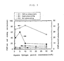
- Fig. 2 is the result of an additional test based on said Japanese Published Unexamined Patent Application No. 7-233485 .
- Fig. 2 shows a concentration of 30% aqueous hydrogen peroxide, and to make a comparison with the above Koho, the results should be multiplied by a factor of 0.3.
- the hard pad IC1000 of the Rodel company was used as a polishing pad.
- the rotation speeds of the platen (diameter: 340 mm) and holder were both 60rpm, and the down force was 220g/cm 2 (same as CMP condition of this invention). From the result of Fig. 2, it is seen that when an abrasive is not included, the CMP rate is barely 20nm/min, i. e. a practical CMP rate is not obtained. When the hydrogen peroxide concentration is low, the etching rate is fast, and stability of polishing becomes poor. The stability rises if the hydrogen peroxide concentration is increased, but the CMP rate becomes very low which is disadvantageous from the viewpoint of throughput.
- the still solution etching rate (the etching rate in the case when a stationary sample was immersed in a polishing solution which was not stirred) does not fall exactly to zero even at high hydrogen peroxide concentration.
- the polishing solution is stirred, and the etching rate is measured (the etching rate in a stirred solution is near to the etching rate during CMP), it is seen that the etching rate increases, and exceeds 1/2 of the polishing rate.
- rate ratio the ratio of the CMP rate and stirred etching rate
- FIG. 22A, 22B A cross-section of the copper interconnection formed is shown in Figs. 22A, 22B. Most of the copper which would have been left in the groove of the silicon dioxide film was etched out. As a result of a continuity test using a meandering pattern (line width 0.3-3 ⁇ m, length 40 mm), the yield was 0%. Therefore, this could not be used as an LSI interconnection. This is due to the fact that as the CMP rate is slow, etching occurred during the long polishing time.
- potassium hydroxide may be added to the polishing solution to adjust the alkalinity to pH10.5.
- a problem occurs in that the selective ratio falls and erosion occurs due to the etching of the silicon dioxide film by potassium hydroxide. Potassium ion which remains behind spreads through the insulating film, and causes deterioration of the characteristics of the semiconductor device.
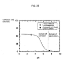
- Fig. 26 shows the difference of corrosion rate (etching rate) in the domain of corrosion and domain of passivation of copper.
- the solid line shows the corrosion rate when the oxidation-reduction potential is the same for the citric acid-based polishing solution and the aminoacetic acid-based polishing solution in Fig. 9.
- corrosion rate was plotted for a polishing solution comprising a mixture of citric acid and aqueous hydrogen peroxide in the domain of corrosion, and a polishing solution comprising a mixture of aminoacetic acid and aqueous hydrogen peroxide in the domain of passivation. Both polishing solutions were prepared with equal mole ratios.
- copper is rendered water-soluble and ionized at a much faster rate than in the domain of passivation.
- This invention which was conceived in view of the aforesaid problems, therefore aims to provide a polishing method and semiconductor manufacturing method which permit at least one of the following to be attained: (1) control of dishing and erosion in the formation of an inlaid interconnection, (2) reduction of scratches, (3) reduction of peeling, (4) simplification of post-CMP cleaning, (5) cost reduction of polishing solutions and polishing pads, (6) simplification of slurry supply/processing equipment, (7) higher throughput, and (8) less dust.
- a metal film polishing method wherein a metal film surface is mechanically rubbed using a polishing solution not comprising a polishing abrasive or comprising a polishing abrasive at a low concentration of less than 1 wt %, and having a pH and oxidation-reduction potential within the domain of corrosion of the metal film.
- a substance for suppressing corrosion may be added to the polishing solution as necessary.
- a polishing solution 1 comprising an oxidizer (substance which removes metal electrons and raises the atomic valence) and a substance which renders oxides water-soluble.
- oxidizer substance which removes metal electrons and raises the atomic valence
- substance which renders oxides water-soluble it may be applied to a metal film of Cu, W, Ti, TiN or Al.
- the above objects are achieved by mechanically rubbing the metal film surface with a polishing solution 2 comprising a substance which renders the aforesaid metal water-soluble.
- a polishing solution 2 comprising a substance which renders the aforesaid metal water-soluble.
- it may be applied to metal films of Al or the like, which are commonly metals having a lower ionization tendency than hydrogen.
- substances which render the metal water-soluble are hydrochloric acid, organic acids, or alkalis such as ammonium hydroxide.
- ammonium hydroxide as the substance which renders the metal water-soluble in the case of copper, which has a higher ionization tendency than hydrogen.
- the metal can be rendered water-soluble, and metal remaining on the surface of the insulating film exposed on the surface of the polished substrate can be reduced.
- the domain of corrosion of each metal is given in the pH-oxidation/reduction potential diagram of Pourbaix mentioned above.
- Cu dissolves as Cu 2+ ion if pH ⁇ 7 and the oxidation reduction potential >0. 2, as shown in Fig. 9. Otherwise, it dissolves as CuO 2 2- ion in the alkaline region of pH>12. 5. Therefore, when polishing copper, it is desirable that it is in either domain of corrosion.
- the Pourbaix diagram relates to an H 2 O system, and when other reagents are contained in the polishing solution, the range of the domain of corrosion in the pH and oxidation-reduction potential diagram will vary.
- the domain of corrosion in the context of this invention is defined by whether or not certain substances, including these substances, are within the range of pH and oxidation-reduction potential in which the polishing solution corrodes the metal.
- the polishing solution contains both a corrosive substance and an inhibitor, the former is within the domain of corrosion shown by this invention.
- the metal surface is first oxidized by the oxidizer, and a thin oxide layer is formed on the surface.
- the oxide layer becomes an aqueous solution, and the thickness of the oxide layer decreases.
- the part of the oxide layer which became thinner is again exposed to the oxidizer, and the thickness of the oxide layer increases. This reaction is repeated as CMP progresses.
- the inhibitor adheres to the metal surface, suppresses the reaction of the depressions and has the final effect of improving flatness. If the polishing solution is within the domain of corrosion of the Pourbaix diagram even when an inhibitor is added, the aforesaid reaction proceeds at the projections on the metal surface where the inhibitor has been removed by rubbing with the polishing pad, and the surface becomes flat. In other words the polishing solution has both a corrosive effect and an inhibitory effect, and it is important to control both effects during CMP.
- the addition concentration of the inhibitor to the polishing solution should be such that inhibitor adhering to the projections on the metal surface is removed by the mechanical friction of the polishing pad.
- the CMP rate is maintained at 50nm/min or more, and that the stirred etching rate should be several nm/min or less (rate ratio of the order of 50).
- the CMP rate may fall. If the CMP rate is sufficiently high without the addition of additives, and the etching rate is no greater than several nm/min, the substrate can be polished to a high degree of flatness even if the inhibitor is not added.
- the metal surface was oxidized by an oxidizer, and the CMP rate was increased by mechanically removing this oxide layer using a polishing abrasive.
- a practical CMP rate is effectively obtained by the mechanical friction of the polishing pad alone by adding a substance which renders the oxide water-soluble.
- Ferric nitrate and potassium iodate contain a metal component, but they have the effect of increasing the CMP rate due to their strong oxidizing power.
- Examples of substances that make the afore said oxide water-soluble are acids, which convert the metal to metal ion (e.g. Cu2+ ion).
- Typical inorganic acids are nitric acid, sulfuric acid and hydrochloric acid.
- Organic acids or their salts have low toxicity and are easy to or handle as a polishing solution.
- Typical examples are hydroxy acid and carboxylic acid such as citric acid, malic acid, malonic acid, succinic acid, phthalic acid, dihydroxysuccinic acid, lactic acid, maleic acid, fumaric acid, pimelic acid, adipic acid, glutaric acid, oxalic acid, salicylic acid, glycolic acid, benzoic acid, formic acid, acetic acid, propionic acid, butyric acid and valeric acid and their salts.
- Salts increase solubility, and preferably comprise ammonium salts, which do not contain a metal component, or an element which does not have an adverse effect on semiconductor elements (e.g. aluminum).
- citric acid malic acid, malonic acid, succinic acid, dihydroxysuccinic acid and formic acid are preferable as the acid used in the polishing solution of this invention due to high CMP rate and low etching rate.
- citric acid and malic acid are generally used as food additives, and due to their low toxicity, low effluent problem, lack of odor and high solubility in water, they are preferable as the acid used in the polishing solution of this invention.
- phthalic acid is used as a polishing solution for copper
- hydrogenphthalate salt is used wherein only one of the two carboxyl groups in the phthalic acid molecule is substituted, the solubility in water increases and the pH can be kept acid (domain of corrosion), so it is suitable as a polishing solution.
- One substance alone may be used both as an oxidizer and as a reagent for rendering the oxide soluble, for example nitric acid which dissolves copper. This makes it possible to reduce the amount of reagent added, so the time and cost required to prepare the polishing solution can be reduced.
- Other oxidizers such as hydrogen peroxide can also be mixed in to increase oxidizing power.
- the substance which renders the oxide water-soluble may be ammonium hydroxide, ammonium nitrate or ammonium chloride.
- Examples of substances which suppress etching or oxidation are inhibitors and surfactants.
- This substance may be a material which, when mixed with the polishing solution, suppresses etching while permitting a sufficient CMP rate to be obtained.
- the most effective inhibitor for copper alloy is benzotriazole (referred to hereafter as BTA).
- BTA benzotriazole
- Other substances with an inhibitory effect are tolyltriazole (referred to hereafter as TTA), BTA derivatives such as BTA carboxylic acids (referred to hereafter as BTA-COOH), cystine, haloacetic acids, glucose and dodecyl mercaptan.
- the effective surfactants are polyacrylic acid, polyammoniumacrylate, polymethacrylic acid, polyammoniummethacrylate.
- the most effective surfactant is polyammoniumacrylate due to high CMP rate and low etching rate.
- a polishing pad may be used wherein more than 1 wt % of polishing abrasive is not supplied to the polishing solution.
- the optimum hardness of the polishing pad is different depending on the object on which CMP is performed, but if for example a copper electrode pattern of 0.1mm side is to be formed, and the permissible amount of dishing is 100nm or less, it is desirable that when the polishing pad is pushed into a 0.1mm opening under the load for performing CMP, the amount by which the polishing pad is compressed and pushed out from the opening is no more than 100nm. A hard polishing pad meets this condition, and by using such a pad, dishing can be suppressed.
- the damascene method is a technique wherein a metal film is formed on an insulating film which has an opening, polished, and the metal film is left in the opening.
- a soft polishing pad can also be used.
- the polishing pad is hard, provided that scratches or peeling is not caused, however it must be sufficiently soft to be able to follow projections on the substrate surface other than the interconnection or plug pattern, such as for example the curve of a wafer.
- the upper limit of polishing abrasive supplied from the polishing pad is different according to the above objects (1)-(8).
- the object (1) of suppressing dishing and erosion is achieved by an abrasive concentration of 0.05 wt % or less.
- a polishing solution having a CMP rate of 10nm/min or less requires 80 min for performing CMP on a metal film of, for example, 800nm. Therefore, it is not practical for preparing an interconnection structure, and as it does not resolve the above problems of throughput and cost, it is not defined as a polishing solution according to this invention.
- the ratio of CMP rate and etching rate is 5 or more, and if possible, 10 or more. If it is less than this, the interconnection structure cannot be formed with high precision due to the etching effect produced in CMP even if the CMP rate is high.
- the etching rate is no higher than several nm/min.
- This invention is most effective for performing CMP on copper alloy or aluminum alloy wherein scratches, dishing and erosion may easily occur. It is also effective for reducing scratches on insulating films in other metal CMP, e. g. tungsten and tungsten alloy, and titanium and titanium alloy (particularly titanium nitride).
- Fig. 1 is a schematic view showing a CMP machine used in this embodiment of the invention.
- a holder 12 which supports a wafer 14 by a backing pad 18 is rotated on a platen 11 to which a polishing pad 17 is attached.
- a retainer ring 13 is provided so that the wafer does not come off during CMP.
- the down force in CMP was 220g/cm 2
- the rotation speed of platen and holder was 60 rpm.
- the down force and rotation speed are not limited to this.
- the CMP rate is faster if the load and rotation speed are increased, but scratches occur more easily as shown in Fig. 25.
- the polishing abrasive concentration is low or zero in this invention, not many scratches occur relative to the load.
- the polishing pad used was the polishing pad IC1000 manufactured by the Rodel company.
- the polishing solution of this invention was dripped from a first supply nozzle 15 provided on the platen onto the polishing pad at a rate of about 30cc/min, and CMP was performed.
- the first supply nozzle 15 was closed to stop supply of polishing solution, and pure water was supplied from a second supply nozzle 16 at a rate of approximately 3000 cc/min to perform rinsing for 15-30 seconds.
- megasonic cleaning was performed to remove polishing solution, and the wafer was dried.
- the basic polishing characteristics of the polishing solution were examined using a wafer on which an interconnection pattern had not been formed.
- a sample was obtained by forming silicon dioxide to a thickness of 200nm on a silicon wafer, and continuously depositing a TiN film of 50nm thickness as adhesion layer and a Cu film of thickness 800nm in vacuum by the sputtering method.
- the diameter of the wafer was 4 inches.
- the polishing solution used in this embodiment was a mixture of an oxidizer and an organic acid, which is a substance for rendering oxide water-soluble.
- the oxidizer was hydrogen peroxide (30% aqueous solution of H 2 O 2 ), and citric acid was used as the organic acid.
- Citric acid has the advantage of high solubility in water. To optimize the mixing ratio, the concentration was varied, and CMP rate and etching rate were examined. The temperature of the polishing solution was room temperature.
- the etching rate is the etching rate of a copper surface when the sample was immersed in the polishing solution. As the interconnection structure cannot be formed when etching during CMP is excessive, the etching rate is preferably as low as possible.
- the still solution etching rate and stirred solution etching rate were examined as in Fig 2. The CMP rate and the etching rate were estimated by converting from the electrical resistivity variation.
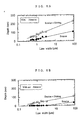
- Fig. 3 shows the result of examining the dependency of the polishing solution on aqueous hydrogen peroxide concentration.
- the citric acid concentration was 0.03 wt %.
- the ratio of the CMP rate to the still solution etching rate is also shown.
- the CMP rate shows a maximum value of 84nm/min when the aqueous hydrogen peroxide concentration is 10 vol %, but as the etching rate has a low value of 5nm/min or less at 5 vol % or lower, the ratio of CMP rate and etching rate shows its highest value of 30 at 5 vol %.
- the CMP rate is 10nm/min or less, which is not sufficient for the purpose of forming an inlaid interconnection. That is, the polishing solution must contain both citric acid and aqueous hydrogen peroxide.
- a copper inlaid interconnection pattern was formed using a polishing solution comprising 5 vol % of aqueous hydrogen peroxide and 0.03 wt % citric acid mixed with pure water. This polishing solution is in the domain of corrosion of copper, as shown in Fig. 9.
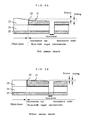
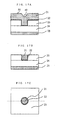
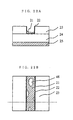
- FIG. 4A A cross-section of a sample with an inlaid interconnection before polishing is shown in Fig. 4A.
- a BPSG film 24 (silicon dioxide to which boron and phosphorus were added) of thickness 500nm and a silicon dioxide film 23 of thickness 500nm were formed on a silicon substrate 25 on which an impurity-doped layer and insulating film had been formed, and an interconnection groove pattern of thickness 500nm was formed in the silicon dioxide layer 23 by a lithography process and dry etching process.
- a copper film of thickness 800nm was continuously formed in vacuum by sputtering. Vacuum heat processing was also performed at 450 °C for 30 min in the sputter machine to improve step covering properties. Impurity-doped layers such as a source and drain were thereby formed in the silicon substrate 25, but these will not be described here.
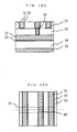
- Figs. 17A - 17C show the structure of a copper plug of 0.5 ⁇ m diameter.
- Fig. 17A is a cross-section of the structure before CMP
- Fig. 17B is a cross-section of the structure after CMP
- Fig. 17C is the structure viewed from above.
- the insulation film opening is no more than one ⁇ m, so the plug could be formed without dishing or erosion as shown in Fig. 17B even using a soft polishing pad (for example, Suba800 or XHGM1158 manufactured by the Rodel company).
- a hard polishing pad (IC1000) may of course also be used.
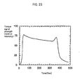
- CMP end point detection was performed without problems.
- a signal shown in Fig. 23 was obtained. Polishing of Cu was completed after approximately 350 seconds elapsed. In the TiN polishing stage, the torque signal strength increased, and the strength dropped after approximately 400 seconds elapsed which was determined as the end point.
- the polishing solution was transparent, but when the copper is polished, copper ion dissolves in the polishing solution which therefore becomes blue.
- citric acid was used as an acid, but the interconnection structure can also be formed if malic acid, malonic acid, succinic acid or dihydroxysuccinic acid is used instead of citric acid.
- hydrogen peroxide was used as an oxidizer, but the interconnection structure can also be formed if ferric nitrate or potassium iodate is used instead of hydrogen peroxide. However, some method is needed against iron or potassium contamination.
- An inlaid interconnection structure may be formed in the same way if CMP is performed using a polishing solution containing ammonium hydroxide, ammonium chloride or ammonium nitrate.
- the etching rate shown in Fig. 3 decreases, and the ratio of CMP rate to etching rate further increases. As a result, excessive etching of the copper surface during CMP can be prevented, and oxidation of the polished copper surface after CMP can be prevented.
- the inhibitor was BTA.
- 0.1 wt % BTA was added to a polishing solution comprising 5 vol % aqueous hydrogen peroxide and 0.03 wt % citric acid mixed with pure water.
- the etching rate was measured as in Embodiment 1, and was found to have decreased to about 1/6 compared with the solution before BTA was added.
- An interconnection structure could also be formed even if the above-mentioned polishing solution was concentrated.
- good results were obtained with a solution comprising 30 vol % aqueous hydrogen peroxide, 0.15 wt % citric acid and 0.3 wt % BTA mixed with pure water.
- the polishing uniformity in the wafer improved, i.e. whereas the uniformity was 10% or more with a dilute polishing solution, it was 8% or less with a concentrated polishing solution.
- a dilute solution has the advantage of being able to be manufactured more cheaply.
- citric acid was used as an acid, but the interconnection structure can also be formed if malic acid, malonic acid, succinic acid or dihydroxysuccinic acid is used instead of citric acid.
- malic acid malonic acid
- succinic acid succinic acid or dihydroxysuccinic acid
- good results were obtained with a solution comprising 30 vol % aqueous hydrogen peroxide, 0.15 wt % malic acid and 0.2 wt % BTA mixed with pure water.
- Embodiment 2 The polishing solution of Embodiment 2 (5 vol % aqueous hydrogen peroxide, 0.03 wt % citric acid and 0.01 % BTA mixed with pure water), and the same polishing solution with 2.5 wt % added alumina abrasive (particle diameter: approx. 200nm) as a comparison, were prepared.
- Figs. 6A, 6B show the measurement results
- Figs. 7A. 7B, 8A, and 8B show sections which were drawn based on the SEM observations.
- Figs. 6A, 6B From Figs. 6A, 6B it is seen that the dishing amount and erosion amount increased as the line width increased. However, the dishing amount decreased to about half by eliminating the alumina abrasive, and the erosion amount at a line width of 4 ⁇ m or less decreased to a level at which it was almost unobservable by SEM (10nm or less). From a comparison of Figs. 8A, 8B, a remarkable difference was observed at a line width of 90 ⁇ m.
- the polishing solution of Embodiment 2 (5 vol % aqueous hydrogen peroxide, 0.03 wt % citric acid and 0.01 % BTA mixed with pure water), and polishing solutions with 0.0001 wt %, 0.001 wt %, 0.01 wt %, 0.05 wt %, 0.1 wt %, 0.5 wt %, 1 wt %, 2.5 wt % and 5 wt % alumina abrasive (particle diameter: approx. 200nm) added to this solution, were prepared.
- CMP was performed using these solutions on a copper thin film surface with no interconnection pattern and a silicon dioxide film surface.
- the down force and platen rotation speed can be increased, so the CMP rate can be increased.
- An inlaid interconnection was formed by the same method as that of Embodiment 1 using the polishing solution having an abrasive concentration of less than 0.1 wt %.
- an effectively 100% yield was obtained.
- the polishing solution of Embodiment 2 (5 vol % aqueous hydrogen peroxide, 0.03 wt % citric acid and 0.01 wt % BTA mixed with pure water), and polishing solutions with 0.0001 wt %, 0.001 wt %, 0.01 wt %, 0.05 wt %, 0.1 wt %, 0.5 wt %, 1 wt %, 5 wt % and 10 wt % alumina abrasive added to this solution, were prepared.
- a sample was prepared by forming a thin copper film of thickness 800nm on a silicon dioxide film surface by sputtering, with a TiN layer of thickness 5nm (1/10 the thickness of Embodiment 1) in between. CMP was performed on this sample using the aforesaid polishing solutions.
- peeling occurred between the copper layer and the TiN layer from the periphery of a wafer on which CMP was performed using a polishing solution having an alumina abrasive concentration of 1 wt % or more. This is considered to be due to the frictional force which occurs between the alumina abrasive and the copper surface.
- the frictional force decreased in a wafer on which CMP was performed using a polishing solution having an alumina abrasive concentration of 0.5 wt % or less, and in this case, no peeling occurred at all. Further, as peeling is reduced, the down force and platen rotation speed can be increased, so the CMP rate can be increased.
- An inlaid interconnection was forme d by the same method as that of Embodiment 2 using the polishing solution having an abrasive concentration of 0.5 wt % or less.
- a sample was used wherein the TiN layer 22 of Figs. 4A - 4C was 5nm. As a result, an inlaid interconnection was formed without any peeling of the thin copper film.
- the polishing solution of Embodiment 2 (5 vol % aqueous hydrogen peroxide, 0.03 wt % citric acid and 0.1 wt % BTA mixed with pure water), and polishing solutions with 0.0001 wt %, 0.001 wt %, 0.01 wt %, 0.05 wt %, 0.1 wt %, 0.5 wt %, 1 wt %, 5 wt % and 10 wt % alumina abrasive added to this solution, were prepared.
- the copper th in film and TiN thin film formed on the silicon dioxide film surface were removed by CMP, and after the silicon dioxide film surface which appeared was washed with pure water, the alumina abrasive (number of defects) which remained was examined with a wafer particle counter.
- the number of defects having a size of 0.2 ⁇ m or larger per wafer was measured.
- the size of the wafer was 4 inches.
- the number of defects decreased according to decrease of alumina abrasive concentration as shown in Fig. 10. and at a concentration of 0.01 wt % or less, the number can be reduced to 100 or less by megasonic cleaning alone.
- the number of CMP processing steps is reduced by reducing the abrasive concentration.
- Fig. 11 shows a CMP process where a prior art polishing solution was used.
- the alumina abrasive concentration was as high as, for example, 1 wt % or more, and conditioning of the polishing pad was performed for several tens of seconds to a few minutes before CMP to prevent clogging of the polishing pad with abrasive.
- CMP was performed on the insulating film from several tens of seconds to about 2 minutes to remove the damaged layer of the insulating film surface, e.g. the silicon dioxide film exposed by polishing. Subsequently, the wafer was subjected to a cleaning step without drying, and a first brush cleaning was performed with ammonia solution to remove abrasive. A second brush cleaning with dilute hydrofluoric acid (HF) was performed to remove metal contamination in the damaged layer of the insulating film surface, e. g. the silicon dioxide film. Finally, after removing abrasive to the desired level by megasonic cleaning, the wafer was dried.
- HF dilute hydrofluoric acid
- Fig. 12 shows the whole CMP process when a polishing solution having a low polishing abrasive concentration of less than 0.01 wt % according to this invention was used. As there is almost no longer any clogging by abrasive in the CMP machine, conditioning is practically unnecessary except in the case of a new polishing pad. If the abrasive concentration was 1/10, the life of the polishing pad was extended 10 times. Also, as there is no damaged layer due to scratching of the silicon dioxide film surface, it is not necessary to perform CMP on the insulating film. In the cleaning step, the prior art level (number of defects) could be attained by megasonic cleaning alone.
- Fig. 12 may be used in practice if the abrasive concentration is 0.01 wt % or less, but it is preferably 0.005 wt % or less.
- the CMP time including over-polishing time for a CMP alumina slurry used for copper CMP is 5 min, and the slurry is supplied to a CMP machine at a rate of 100cc/min, one liter is used for one CMP.
- One polishing pad is consumed approximately every 400 wafers.
- a post-cleaning machine is necessary.
- CMP costs are largely reduced by decreasing the alumina abrasive concentration to 0.001 wt % or less.
- the reagents added to the polishing solution are still required, but the cost is of the order of 1/100 of a prior art alumina slurry. Further, as the conditioning frequency in the prior art is less, the cost of polishing pads can also be reduced.
- the alumina abrasive concentration is 0.0001 wt % or less, a slurry supply equipment, slurry stirring equipment and slurry processing equipment are unnecessary, and if the alumina abrasive concentration is zero, there is no need for dust prevention measures in the clean room and costs can be largely reduced compared to the prior art machine.
- cleaning machine brush-cleaning is unnecessary, so the cost is about half. Hence, about 70% of the cost of CMP as a whole can be reduced by using the polishing solution of this invention.
- Nitric acid has an oxidizing action on copper, and as copper is made water-soluble by the acidic nature of nitric acid, two of the functions of this invention may be realized by one reagent.
- BTA suppresses etching as in the case of Embodiment 2, so the ratio of CMP rate and etching rate is increased. Excessive etching of the copper surface during CMP can therefore be prevented, and excessive oxidation of the polished copper surface after CMP can also be prevented.
- the polishing solution is an aqueous solution comprising nitric acid: 0.2 vol % and BTA: 0.01 wt % mixed with pure water. This polishing solution is in the domain of corrosion of copper, as shown in Fig. 9.
- the etching rate of copper was examined as in Embodiment 1, and found to be reduced to about 1/6 due to the addition of BTA.
- CMP was performed using this polishing solution under the same conditions as those of Embodiment 1, corrosion of the polished copper surface was prevented and an inlaid interconnection could be formed.
- the copper interconnection part is etched and was observed to be more depressed than the surrounding insulating film (in particular, the copper disappeared when the nitric acid concentration was as high as 1 vol % or more). This was suppressed to several 10nm or less as shown in Fig. 16B when a polishing solution with added BTA was used.
- a multilayered interconnection structure was prepared using the polishing solution of Embodiment 2 (30 vol % aqueous hydrogen peroxide, 0.15 wt % malic acid and 0.2 wt % BTA mixed with pure water), and experiments were performed to demonstrate its effect.
- CMP was performed using a prior art polishing solution comprising 1 wt % of alumina abrasive.
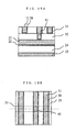
- Figs. 14A - 14C show a two-layer interconnection structure obtained as a result of performing CMP using a prior art polishing solution.
- a semiconductor device was manufactured comprising diffusion layers such as a source and drain in a silicon substrate 25, but this will not be described here (same for Figs. 15 - 20).
- 39 is a TiN layer and 52 is a throughhole layer insulating film.
- Figs. 18A and 18B show a part wherein the first layer interconnection 21 and second layer interconnection 31 are connected by a copper plug 40.
- This device was manufactured by performing CMP using the aforesaid polishing solution on each layer including the plug. There were no electrical short-circuits whatever due to the dishing, erosion and scratches shown in Figs. 14A - 14B.
- a multi-layer interconnection could also be formed in the same way using the polishing solutions described in Embodiment 1 and Embodiment 9.
- the plug may also be formed by a tungsten film using the CVD method which has a high coverage performance, as shown in Figs. 20A - 20B.
- a seam 43 (known also as a keyhole, etc.) is easily formed in the center part of the plug, and polishing solution may seep into the interior of the device and rapidly corrode the base copper interconnection 21.
- Fig. 20A shows this situation.
- 44 is a corroded copper interconnection part.
- a copper inhibitor for example BTA
- Fig. 19 sho ws a sample wherein a two-layer interconnection is formed by a dual damascene method.
- This is a technique wherein a plug for the first layer interconnection and the second layer interconnection are polished in one step. After polishing the first layer interconnection with the aforesaid polishing solution, the plug and second layer interconnection were then polished by CMP with the aforesaid polishing solution.
- Numeral 41 is the plug formed by the dual damascene method. There were no electrical short-circuits whatever due to the dishing, erosion and scratches shown in Figs. 14A and 14B. A multi-layer interconnection could also be formed in the same way using the polishing solutions described in Embodiment 1 and Embodiment 9.
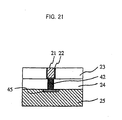
- Fig. 21 shows a situation wherein a tungsten plug 42 is formed on an impurity-doped layer 45 of a silicon substrate and connected to the copper interconnection 21 using the polishing solution of this invention. It was confirmed that, by forming a multi-layer interconnection as described hereabove on this upper layer, an LSI could be manufactured and operated by connecting different semiconductor devices.
Landscapes
- Engineering & Computer Science (AREA)
- Chemical & Material Sciences (AREA)
- Condensed Matter Physics & Semiconductors (AREA)
- General Physics & Mathematics (AREA)
- Manufacturing & Machinery (AREA)
- Computer Hardware Design (AREA)
- Microelectronics & Electronic Packaging (AREA)
- Power Engineering (AREA)
- Physics & Mathematics (AREA)
- Organic Chemistry (AREA)
- Mechanical Engineering (AREA)
- Materials Engineering (AREA)
- Chemical Kinetics & Catalysis (AREA)
- General Chemical & Material Sciences (AREA)
- Metallurgy (AREA)
- Mechanical Treatment Of Semiconductor (AREA)
- Finish Polishing, Edge Sharpening, And Grinding By Specific Grinding Devices (AREA)
Applications Claiming Priority (2)
| Application Number | Priority Date | Filing Date | Title |
|---|---|---|---|
| JP29993797A JP3371775B2 (ja) | 1997-10-31 | 1997-10-31 | 研磨方法 |
| EP98308923A EP0913442B1 (de) | 1997-10-31 | 1998-10-30 | Polierverfahren |
Related Parent Applications (1)
| Application Number | Title | Priority Date | Filing Date |
|---|---|---|---|
| EP98308923A Division EP0913442B1 (de) | 1997-10-31 | 1998-10-30 | Polierverfahren |
Publications (1)
| Publication Number | Publication Date |
|---|---|
| EP1760127A2 true EP1760127A2 (de) | 2007-03-07 |
Family
ID=17878748
Family Applications (2)
| Application Number | Title | Priority Date | Filing Date |
|---|---|---|---|
| EP98308923A Expired - Lifetime EP0913442B1 (de) | 1997-10-31 | 1998-10-30 | Polierverfahren |
| EP06020541A Withdrawn EP1760127A2 (de) | 1997-10-31 | 1998-10-30 | Polierverfahren |
Family Applications Before (1)
| Application Number | Title | Priority Date | Filing Date |
|---|---|---|---|
| EP98308923A Expired - Lifetime EP0913442B1 (de) | 1997-10-31 | 1998-10-30 | Polierverfahren |
Country Status (8)
| Country | Link |
|---|---|
| US (5) | US6117775A (de) |
| EP (2) | EP0913442B1 (de) |
| JP (1) | JP3371775B2 (de) |
| KR (2) | KR100624589B1 (de) |
| CN (2) | CN1974129A (de) |
| DE (1) | DE69836612T2 (de) |
| SG (1) | SG95588A1 (de) |
| TW (1) | TW380083B (de) |
Families Citing this family (194)
| Publication number | Priority date | Publication date | Assignee | Title |
|---|---|---|---|---|
| US8092707B2 (en) | 1997-04-30 | 2012-01-10 | 3M Innovative Properties Company | Compositions and methods for modifying a surface suited for semiconductor fabrication |
| JP3371775B2 (ja) * | 1997-10-31 | 2003-01-27 | 株式会社日立製作所 | 研磨方法 |
| JP2000040679A (ja) | 1998-07-24 | 2000-02-08 | Hitachi Ltd | 半導体集積回路装置の製造方法 |
| JP2000183003A (ja) * | 1998-10-07 | 2000-06-30 | Toshiba Corp | 銅系金属用研磨組成物および半導体装置の製造方法 |
| US6143656A (en) * | 1998-10-22 | 2000-11-07 | Advanced Micro Devices, Inc. | Slurry for chemical mechanical polishing of copper |
| SG99289A1 (en) * | 1998-10-23 | 2003-10-27 | Ibm | Chemical-mechanical planarization of metallurgy |
| US7338908B1 (en) * | 2003-10-20 | 2008-03-04 | Novellus Systems, Inc. | Method for fabrication of semiconductor interconnect structure with reduced capacitance, leakage current, and improved breakdown voltage |
| US6245690B1 (en) | 1998-11-04 | 2001-06-12 | Applied Materials, Inc. | Method of improving moisture resistance of low dielectric constant films |
| US6276996B1 (en) | 1998-11-10 | 2001-08-21 | Micron Technology, Inc. | Copper chemical-mechanical polishing process using a fixed abrasive polishing pad and a copper layer chemical-mechanical polishing solution specifically adapted for chemical-mechanical polishing with a fixed abrasive pad |
| US6206756B1 (en) | 1998-11-10 | 2001-03-27 | Micron Technology, Inc. | Tungsten chemical-mechanical polishing process using a fixed abrasive polishing pad and a tungsten layer chemical-mechanical polishing solution specifically adapted for chemical-mechanical polishing with a fixed abrasive pad |
| JP2000228391A (ja) * | 1998-11-30 | 2000-08-15 | Canon Inc | 半導体基板の精密研磨方法および装置 |
| WO2000039844A1 (fr) * | 1998-12-28 | 2000-07-06 | Hitachi Chemical Company, Ltd. | Materiaux pour liquide de polissage de metal, liquide de polissage de metal, procede de preparation et procede de polissage connexes |
| JP3033574B1 (ja) * | 1999-02-15 | 2000-04-17 | 日本電気株式会社 | 研磨方法 |
| JP4127926B2 (ja) | 1999-04-08 | 2008-07-30 | 株式会社荏原製作所 | ポリッシング方法 |
| JP2000311876A (ja) * | 1999-04-27 | 2000-11-07 | Hitachi Ltd | 配線基板の製造方法および製造装置 |
| JP2000315666A (ja) * | 1999-04-28 | 2000-11-14 | Hitachi Ltd | 半導体集積回路装置の製造方法 |
| US6419554B2 (en) * | 1999-06-24 | 2002-07-16 | Micron Technology, Inc. | Fixed abrasive chemical-mechanical planarization of titanium nitride |
| JP4554011B2 (ja) | 1999-08-10 | 2010-09-29 | ルネサスエレクトロニクス株式会社 | 半導体集積回路装置の製造方法 |
| US6855266B1 (en) | 1999-08-13 | 2005-02-15 | Cabot Microelectronics Corporation | Polishing system with stopping compound and method of its use |
| EP1218464B1 (de) * | 1999-08-13 | 2008-08-20 | Cabot Microelectronics Corporation | Chemisch-mechanische poliersysteme und verfahren zu ihrer verwendung |
| IL147236A0 (en) | 1999-08-13 | 2002-08-14 | Cabot Microelectronics Corp | Polishing system and method of its use |
| TW501197B (en) | 1999-08-17 | 2002-09-01 | Hitachi Chemical Co Ltd | Polishing compound for chemical mechanical polishing and method for polishing substrate |
| US6436302B1 (en) * | 1999-08-23 | 2002-08-20 | Applied Materials, Inc. | Post CU CMP polishing for reduced defects |
| US6443812B1 (en) * | 1999-08-24 | 2002-09-03 | Rodel Holdings Inc. | Compositions for insulator and metal CMP and methods relating thereto |
| JP4832690B2 (ja) * | 1999-08-24 | 2011-12-07 | ローム アンド ハース エレクトロニック マテリアルズ シーエムピー ホウルディングス インコーポレイテッド | 絶縁体及び金属のcmp用組成物及びそれに関する方法 |
| CN1161826C (zh) | 1999-08-26 | 2004-08-11 | 日立化成工业株式会社 | 化学机械研磨用研磨剂及研磨方法 |
| US6492273B1 (en) | 1999-08-31 | 2002-12-10 | Micron Technology, Inc. | Methods and apparatuses for monitoring and controlling mechanical or chemical-mechanical planarization of microelectronic substrate assemblies |
| US6376381B1 (en) * | 1999-08-31 | 2002-04-23 | Micron Technology, Inc. | Planarizing solutions, planarizing machines, and methods for mechanical and/or chemical-mechanical planarization of microelectronic substrate assemblies |
| JP4513145B2 (ja) * | 1999-09-07 | 2010-07-28 | ソニー株式会社 | 半導体装置の製造方法および研磨方法 |
| JP4759779B2 (ja) * | 1999-09-09 | 2011-08-31 | 日立化成工業株式会社 | 基板の研磨方法 |
| US6620725B1 (en) * | 1999-09-13 | 2003-09-16 | Taiwan Semiconductor Manufacturing Company | Reduction of Cu line damage by two-step CMP |
| CN1125862C (zh) * | 1999-09-20 | 2003-10-29 | 长兴化学工业股份有限公司 | 半导体加工用化学机械研磨组合物 |
| US6656842B2 (en) * | 1999-09-22 | 2003-12-02 | Applied Materials, Inc. | Barrier layer buffing after Cu CMP |
| US6303506B1 (en) * | 1999-09-30 | 2001-10-16 | Infineon Technologies Ag | Compositions for and method of reducing/eliminating scratches and defects in silicon dioxide during CMP process |
| JP3307375B2 (ja) * | 1999-10-04 | 2002-07-24 | 日本電気株式会社 | 半導体装置の製造方法 |
| US6435944B1 (en) | 1999-10-27 | 2002-08-20 | Applied Materials, Inc. | CMP slurry for planarizing metals |
| US6720264B2 (en) * | 1999-11-04 | 2004-04-13 | Advanced Micro Devices, Inc. | Prevention of precipitation defects on copper interconnects during CMP by use of solutions containing organic compounds with silica adsorption and copper corrosion inhibiting properties |
| JP3439402B2 (ja) * | 1999-11-05 | 2003-08-25 | Necエレクトロニクス株式会社 | 半導体装置の製造方法 |
| US6432826B1 (en) * | 1999-11-29 | 2002-08-13 | Applied Materials, Inc. | Planarized Cu cleaning for reduced defects |
| US6638143B2 (en) | 1999-12-22 | 2003-10-28 | Applied Materials, Inc. | Ion exchange materials for chemical mechanical polishing |
| JP3805588B2 (ja) | 1999-12-27 | 2006-08-02 | 株式会社日立製作所 | 半導体装置の製造方法 |
| US6881674B2 (en) | 1999-12-28 | 2005-04-19 | Intel Corporation | Abrasives for chemical mechanical polishing |
| JP3490038B2 (ja) * | 1999-12-28 | 2004-01-26 | Necエレクトロニクス株式会社 | 金属配線形成方法 |
| TW572980B (en) | 2000-01-12 | 2004-01-21 | Jsr Corp | Aqueous dispersion for chemical mechanical polishing and chemical mechanical polishing process |
| US6797623B2 (en) * | 2000-03-09 | 2004-09-28 | Sony Corporation | Methods of producing and polishing semiconductor device and polishing apparatus |
| US6228771B1 (en) * | 2000-03-23 | 2001-05-08 | Infineon Technologies North America Corp. | Chemical mechanical polishing process for low dishing of metal lines in semiconductor wafer fabrication |
| JP2001269859A (ja) | 2000-03-27 | 2001-10-02 | Jsr Corp | 化学機械研磨用水系分散体 |
| US6451697B1 (en) | 2000-04-06 | 2002-09-17 | Applied Materials, Inc. | Method for abrasive-free metal CMP in passivation domain |
| US6943113B1 (en) * | 2000-05-11 | 2005-09-13 | Infineon Technologies Ag | Metal chemical polishing process for minimizing dishing during semiconductor wafer fabrication |
| US6858540B2 (en) * | 2000-05-11 | 2005-02-22 | Applied Materials, Inc. | Selective removal of tantalum-containing barrier layer during metal CMP |
| JP3945964B2 (ja) * | 2000-06-01 | 2007-07-18 | 株式会社ルネサステクノロジ | 研磨剤、研磨方法及び半導体装置の製造方法 |
| JP4743941B2 (ja) * | 2000-06-30 | 2011-08-10 | Jsr株式会社 | 化学機械研磨用水系分散体 |
| US6653242B1 (en) | 2000-06-30 | 2003-11-25 | Applied Materials, Inc. | Solution to metal re-deposition during substrate planarization |
| JP3837277B2 (ja) | 2000-06-30 | 2006-10-25 | 株式会社東芝 | 銅の研磨に用いる化学機械研磨用水系分散体及び化学機械研磨方法 |
| KR100338777B1 (ko) * | 2000-07-22 | 2002-05-31 | 윤종용 | 화학 기계적 연마 이후의 구리층 부식을 방지하는 반도체장치 제조방법 및 이에 이용되는 화학 기계적 연마장치 |
| JP2002043256A (ja) * | 2000-07-27 | 2002-02-08 | Hitachi Ltd | 半導体ウエハ平坦化加工方法及び平坦化加工装置 |
| US6872329B2 (en) | 2000-07-28 | 2005-03-29 | Applied Materials, Inc. | Chemical mechanical polishing composition and process |
| JP2002050595A (ja) | 2000-08-04 | 2002-02-15 | Hitachi Ltd | 研磨方法、配線形成方法及び半導体装置の製造方法 |
| US6602436B2 (en) | 2000-08-11 | 2003-08-05 | Rodel Holdings, Inc | Chemical mechanical planarization of metal substrates |
| US7192888B1 (en) | 2000-08-21 | 2007-03-20 | Micron Technology, Inc. | Low selectivity deposition methods |
| US7220322B1 (en) | 2000-08-24 | 2007-05-22 | Applied Materials, Inc. | Cu CMP polishing pad cleaning |
| US6605537B2 (en) | 2000-10-27 | 2003-08-12 | Rodel Holdings, Inc. | Polishing of metal substrates |
| WO2002024413A2 (en) * | 2000-09-20 | 2002-03-28 | Rodel Holdings, Inc. | Polishing by cmp for optimized planarization |
| US6503834B1 (en) * | 2000-10-03 | 2003-01-07 | International Business Machines Corp. | Process to increase reliability CuBEOL structures |
| JP2002117670A (ja) | 2000-10-04 | 2002-04-19 | Mitsubishi Electric Corp | 半導体記憶装置 |
| US6461227B1 (en) * | 2000-10-17 | 2002-10-08 | Cabot Microelectronics Corporation | Method of polishing a memory or rigid disk with an ammonia-and/or halide-containing composition |
| US6569349B1 (en) | 2000-10-23 | 2003-05-27 | Applied Materials Inc. | Additives to CMP slurry to polish dielectric films |
| US6524167B1 (en) | 2000-10-27 | 2003-02-25 | Applied Materials, Inc. | Method and composition for the selective removal of residual materials and barrier materials during substrate planarization |
| US6709316B1 (en) | 2000-10-27 | 2004-03-23 | Applied Materials, Inc. | Method and apparatus for two-step barrier layer polishing |
| US20020068454A1 (en) | 2000-12-01 | 2002-06-06 | Applied Materials, Inc. | Method and composition for the removal of residual materials during substrate planarization |
| KR100407296B1 (ko) * | 2000-12-18 | 2003-11-28 | 주식회사 하이닉스반도체 | 티타늄알루미늄나이트라이드의 화학적기계적연마 방법 |
| US6896776B2 (en) | 2000-12-18 | 2005-05-24 | Applied Materials Inc. | Method and apparatus for electro-chemical processing |
| CN1426343A (zh) * | 2000-12-22 | 2003-06-25 | 皇家菲利浦电子有限公司 | 采用上游和下游流体分配装置的化学机械抛光方法和设备 |
| US7012025B2 (en) * | 2001-01-05 | 2006-03-14 | Applied Materials Inc. | Tantalum removal during chemical mechanical polishing |
| US6579439B1 (en) | 2001-01-12 | 2003-06-17 | Southern Industrial Chemicals, Inc. | Electrolytic aluminum polishing processes |
| US6530824B2 (en) * | 2001-03-09 | 2003-03-11 | Rodel Holdings, Inc. | Method and composition for polishing by CMP |
| US7160432B2 (en) * | 2001-03-14 | 2007-01-09 | Applied Materials, Inc. | Method and composition for polishing a substrate |
| US7582564B2 (en) | 2001-03-14 | 2009-09-01 | Applied Materials, Inc. | Process and composition for conductive material removal by electrochemical mechanical polishing |
| US7323416B2 (en) | 2001-03-14 | 2008-01-29 | Applied Materials, Inc. | Method and composition for polishing a substrate |
| US6899804B2 (en) * | 2001-04-10 | 2005-05-31 | Applied Materials, Inc. | Electrolyte composition and treatment for electrolytic chemical mechanical polishing |
| US7232514B2 (en) * | 2001-03-14 | 2007-06-19 | Applied Materials, Inc. | Method and composition for polishing a substrate |
| US6811680B2 (en) * | 2001-03-14 | 2004-11-02 | Applied Materials Inc. | Planarization of substrates using electrochemical mechanical polishing |
| US7128825B2 (en) | 2001-03-14 | 2006-10-31 | Applied Materials, Inc. | Method and composition for polishing a substrate |
| US6627550B2 (en) | 2001-03-27 | 2003-09-30 | Micron Technology, Inc. | Post-planarization clean-up |
| US6568997B2 (en) | 2001-04-05 | 2003-05-27 | Rodel Holdings, Inc. | CMP polishing composition for semiconductor devices containing organic polymer particles |
| US6849547B2 (en) * | 2001-04-05 | 2005-02-01 | Speedfam Ipec Corporation | Apparatus and process for polishing a workpiece |
| JP2004533115A (ja) | 2001-04-12 | 2004-10-28 | ロデール ホールディングス インコーポレイテッド | 界面活性剤を有する研磨用組成物 |
| KR20020083264A (ko) * | 2001-04-26 | 2002-11-02 | 삼성전자 주식회사 | 화학적 기계적 연마용 슬러리와 그 제조방법 |
| US6632259B2 (en) | 2001-05-18 | 2003-10-14 | Rodel Holdings, Inc. | Chemical mechanical polishing compositions and methods relating thereto |
| US6783432B2 (en) | 2001-06-04 | 2004-08-31 | Applied Materials Inc. | Additives for pressure sensitive polishing compositions |
| JP2002368084A (ja) * | 2001-06-12 | 2002-12-20 | Hitachi Ltd | 半導体集積回路装置の製造方法 |
| US6790768B2 (en) * | 2001-07-11 | 2004-09-14 | Applied Materials Inc. | Methods and apparatus for polishing substrates comprising conductive and dielectric materials with reduced topographical defects |
| US6592742B2 (en) | 2001-07-13 | 2003-07-15 | Applied Materials Inc. | Electrochemically assisted chemical polish |
| US7104869B2 (en) * | 2001-07-13 | 2006-09-12 | Applied Materials, Inc. | Barrier removal at low polish pressure |
| US7008554B2 (en) * | 2001-07-13 | 2006-03-07 | Applied Materials, Inc. | Dual reduced agents for barrier removal in chemical mechanical polishing |
| US6821881B2 (en) * | 2001-07-25 | 2004-11-23 | Applied Materials, Inc. | Method for chemical mechanical polishing of semiconductor substrates |
| US20040197541A1 (en) * | 2001-08-02 | 2004-10-07 | Joseph Zahka | Selective electroless deposition and interconnects made therefrom |
| JP2003051481A (ja) * | 2001-08-07 | 2003-02-21 | Hitachi Ltd | 半導体集積回路装置の製造方法 |
| TW583731B (en) * | 2001-08-23 | 2004-04-11 | Mykrolis Corp | Process, system, and liquid composition for selectively removing a metal film |
| US6800218B2 (en) * | 2001-08-23 | 2004-10-05 | Advanced Technology Materials, Inc. | Abrasive free formulations for chemical mechanical polishing of copper and associated materials and method of using same |
| US6812193B2 (en) | 2001-08-31 | 2004-11-02 | International Business Machines Corporation | Slurry for mechanical polishing (CMP) of metals and use thereof |
| US6638326B2 (en) * | 2001-09-25 | 2003-10-28 | Ekc Technology, Inc. | Compositions for chemical mechanical planarization of tantalum and tantalum nitride |
| US20030077983A1 (en) * | 2001-10-12 | 2003-04-24 | International Business Machines Corporation | Cleaning polish etch composition and process for a superfinished surface of a substrate |
| US7077880B2 (en) * | 2004-01-16 | 2006-07-18 | Dupont Air Products Nanomaterials Llc | Surface modified colloidal abrasives, including stable bimetallic surface coated silica sols for chemical mechanical planarization |
| WO2003038883A1 (en) * | 2001-10-31 | 2003-05-08 | Hitachi Chemical Co., Ltd. | Polishing fluid and polishing method |
| US6821897B2 (en) * | 2001-12-05 | 2004-11-23 | Cabot Microelectronics Corporation | Method for copper CMP using polymeric complexing agents |
| KR100445757B1 (ko) * | 2001-12-28 | 2004-08-25 | 제일모직주식회사 | 금속배선 연마용 슬러리 조성물 |
| US20030134576A1 (en) * | 2002-01-17 | 2003-07-17 | Saket Chadda | Method for polishing copper on a workpiece surface |
| US20060255016A1 (en) * | 2002-01-17 | 2006-11-16 | Novellus Systems, Inc. | Method for polishing copper on a workpiece surface |
| US7524346B2 (en) * | 2002-01-25 | 2009-04-28 | Dupont Air Products Nanomaterials Llc | Compositions of chemical mechanical planarization slurries contacting noble-metal-featured substrates |
| JP4187497B2 (ja) * | 2002-01-25 | 2008-11-26 | Jsr株式会社 | 半導体基板の化学機械研磨方法 |
| US7513920B2 (en) * | 2002-02-11 | 2009-04-07 | Dupont Air Products Nanomaterials Llc | Free radical-forming activator attached to solid and used to enhance CMP formulations |
| US20030162398A1 (en) * | 2002-02-11 | 2003-08-28 | Small Robert J. | Catalytic composition for chemical-mechanical polishing, method of using same, and substrate treated with same |
| US6776810B1 (en) | 2002-02-11 | 2004-08-17 | Cabot Microelectronics Corporation | Anionic abrasive particles treated with positively charged polyelectrolytes for CMP |
| KR20030070191A (ko) * | 2002-02-21 | 2003-08-29 | 주식회사 동진쎄미켐 | 안정성 및 탄탈계 금속막에 대한 연마 속도가 우수한화학-기계적 연마 슬러리 조성물 |
| US6821309B2 (en) * | 2002-02-22 | 2004-11-23 | University Of Florida | Chemical-mechanical polishing slurry for polishing of copper or silver films |
| JP3749867B2 (ja) * | 2002-03-08 | 2006-03-01 | 株式会社東芝 | アルミニウム系金属用研磨液および半導体装置の製造方法 |
| CN1444259A (zh) * | 2002-03-12 | 2003-09-24 | 株式会社东芝 | 半导体器件的制造方法 |
| JP2004006628A (ja) * | 2002-03-27 | 2004-01-08 | Hitachi Ltd | 半導体装置の製造方法 |
| KR100476890B1 (ko) * | 2002-04-11 | 2005-03-17 | 삼성전자주식회사 | 검사패턴 및 이를 이용한 화학적기계적 연마공정 제어방법 |
| JP2003318140A (ja) * | 2002-04-26 | 2003-11-07 | Applied Materials Inc | 研磨方法及び装置 |
| US20030209523A1 (en) * | 2002-05-09 | 2003-11-13 | Applied Materials, Inc. | Planarization by chemical polishing for ULSI applications |
| US6936543B2 (en) * | 2002-06-07 | 2005-08-30 | Cabot Microelectronics Corporation | CMP method utilizing amphiphilic nonionic surfactants |
| US6974777B2 (en) * | 2002-06-07 | 2005-12-13 | Cabot Microelectronics Corporation | CMP compositions for low-k dielectric materials |
| US7037174B2 (en) * | 2002-10-03 | 2006-05-02 | Applied Materials, Inc. | Methods for reducing delamination during chemical mechanical polishing |
| KR100500517B1 (ko) * | 2002-10-22 | 2005-07-12 | 삼성전자주식회사 | 반도체 웨이퍼용 cmp 설비 |
| US20040175942A1 (en) * | 2003-01-03 | 2004-09-09 | Chang Song Y. | Composition and method used for chemical mechanical planarization of metals |
| US7300602B2 (en) * | 2003-01-23 | 2007-11-27 | Rohm And Haas Electronic Materials Cmp Holdings, Inc. | Selective barrier metal polishing solution |
| US7390429B2 (en) | 2003-06-06 | 2008-06-24 | Applied Materials, Inc. | Method and composition for electrochemical mechanical polishing processing |
| US6936534B2 (en) * | 2003-09-17 | 2005-08-30 | Micron Technology, Inc. | Method for the post-etch cleaning of multi-level damascene structures having underlying copper metallization |
| US20050092620A1 (en) * | 2003-10-01 | 2005-05-05 | Applied Materials, Inc. | Methods and apparatus for polishing a substrate |
| USPP17182P3 (en) * | 2003-10-02 | 2006-11-07 | Plantas De Navarra S.A. | Peach tree plant named ‘Plawhite 5’ |
| US7427361B2 (en) * | 2003-10-10 | 2008-09-23 | Dupont Air Products Nanomaterials Llc | Particulate or particle-bound chelating agents |
| US8530359B2 (en) * | 2003-10-20 | 2013-09-10 | Novellus Systems, Inc. | Modulated metal removal using localized wet etching |
| US7972970B2 (en) | 2003-10-20 | 2011-07-05 | Novellus Systems, Inc. | Fabrication of semiconductor interconnect structure |
| US7531463B2 (en) * | 2003-10-20 | 2009-05-12 | Novellus Systems, Inc. | Fabrication of semiconductor interconnect structure |
| US8158532B2 (en) * | 2003-10-20 | 2012-04-17 | Novellus Systems, Inc. | Topography reduction and control by selective accelerator removal |
| US8372757B2 (en) * | 2003-10-20 | 2013-02-12 | Novellus Systems, Inc. | Wet etching methods for copper removal and planarization in semiconductor processing |
| US20050112292A1 (en) * | 2003-11-25 | 2005-05-26 | Parker Russell A. | Methods for treating at least one member of a microarray structure and methods of using the same |
| US7465408B1 (en) * | 2003-12-03 | 2008-12-16 | Advanced Micro Devices, Inc. | Solutions for controlled, selective etching of copper |
| US20050139292A1 (en) * | 2003-12-31 | 2005-06-30 | Suresh Ramarajan | Method and apparatus for minimizing thickness-to-planarity and dishing in CMP |
| US7390744B2 (en) | 2004-01-29 | 2008-06-24 | Applied Materials, Inc. | Method and composition for polishing a substrate |
| US7087564B2 (en) * | 2004-03-05 | 2006-08-08 | Air Liquide America, L.P. | Acidic chemistry for post-CMP cleaning |
| US7497967B2 (en) * | 2004-03-24 | 2009-03-03 | Rohm And Haas Electronic Materials Cmp Holdings, Inc. | Compositions and methods for polishing copper |
| US7253111B2 (en) * | 2004-04-21 | 2007-08-07 | Rohm And Haas Electronic Materials Cmp Holding, Inc. | Barrier polishing solution |
| JP2005317808A (ja) * | 2004-04-28 | 2005-11-10 | Nitta Haas Inc | 薄膜研磨用研磨布およびそれを用いる薄膜の研磨方法 |
| US20050252547A1 (en) * | 2004-05-11 | 2005-11-17 | Applied Materials, Inc. | Methods and apparatus for liquid chemical delivery |
| US7303993B2 (en) * | 2004-07-01 | 2007-12-04 | Rohm And Haas Electronic Materials Cmp Holdings, Inc. | Chemical mechanical polishing compositions and methods relating thereto |
| US7384871B2 (en) * | 2004-07-01 | 2008-06-10 | Rohm And Haas Electronic Materials Cmp Holdings, Inc. | Chemical mechanical polishing compositions and methods relating thereto |
| JP4292117B2 (ja) * | 2004-07-15 | 2009-07-08 | Jsr株式会社 | 化学機械研磨用水系分散体及び化学機械研磨方法 |
| US7210988B2 (en) * | 2004-08-24 | 2007-05-01 | Applied Materials, Inc. | Method and apparatus for reduced wear polishing pad conditioning |
| JP2006080388A (ja) * | 2004-09-10 | 2006-03-23 | Nitta Haas Inc | 金属研磨用組成物 |
| US20080105651A1 (en) * | 2004-09-14 | 2008-05-08 | Katsumi Mabuchi | Polishing Slurry for Cmp |
| US7084064B2 (en) | 2004-09-14 | 2006-08-01 | Applied Materials, Inc. | Full sequence metal and barrier layer electrochemical mechanical processing |
| US20060110923A1 (en) * | 2004-11-24 | 2006-05-25 | Zhendong Liu | Barrier polishing solution |
| US7435356B2 (en) * | 2004-11-24 | 2008-10-14 | Rohm And Haas Electronic Materials Cmp Holdings, Inc. | Abrasive-free chemical mechanical polishing compositions and methods relating thereto |
| US7086935B2 (en) * | 2004-11-24 | 2006-08-08 | Rohm And Haas Electronic Materials Cmp Holdings, Inc. | Cellulose-containing polishing compositions and methods relating thereto |
| US7427362B2 (en) * | 2005-01-26 | 2008-09-23 | Rohm And Haas Electronic Materials Cmp Holdings, Inc. | Corrosion-resistant barrier polishing solution |
| US7381646B2 (en) * | 2005-08-15 | 2008-06-03 | Chartered Semiconductor Manufacturing, Ltd. | Method for using a Cu BEOL process to fabricate an integrated circuit (IC) originally having an al design |
| US7442637B2 (en) * | 2005-08-15 | 2008-10-28 | Chartered Semiconductor Manufacturing, Ltd | Method for processing IC designs for different metal BEOL processes |
| KR101423579B1 (ko) * | 2005-08-22 | 2014-07-25 | 어플라이드 머티어리얼스, 인코포레이티드 | 화학적 기계적 폴리싱의 스펙트럼 기반 모니터링을 위한 장치 및 방법 |
| US7306507B2 (en) | 2005-08-22 | 2007-12-11 | Applied Materials, Inc. | Polishing pad assembly with glass or crystalline window |
| US7605082B1 (en) | 2005-10-13 | 2009-10-20 | Novellus Systems, Inc. | Capping before barrier-removal IC fabrication method |
| US7435162B2 (en) * | 2005-10-24 | 2008-10-14 | 3M Innovative Properties Company | Polishing fluids and methods for CMP |
| WO2007094869A2 (en) | 2005-10-31 | 2007-08-23 | Applied Materials, Inc. | Electrochemical method for ecmp polishing pad conditioning |
| US7226345B1 (en) | 2005-12-09 | 2007-06-05 | The Regents Of The University Of California | CMP pad with designed surface features |
| TWI343945B (en) | 2005-12-27 | 2011-06-21 | Hitachi Chemical Co Ltd | Slurry for metal polishing and polishing method of polished film |
| US20070151866A1 (en) * | 2006-01-05 | 2007-07-05 | Applied Materials, Inc. | Substrate polishing with surface pretreatment |
| US20070158207A1 (en) * | 2006-01-06 | 2007-07-12 | Applied Materials, Inc. | Methods for electrochemical processing with pre-biased cells |
| US20070227902A1 (en) * | 2006-03-29 | 2007-10-04 | Applied Materials, Inc. | Removal profile tuning by adjusting conditioning sweep profile on a conductive pad |
| CN101584028A (zh) * | 2006-04-26 | 2009-11-18 | Nxp股份有限公司 | 制造半导体器件的方法、由此获得的半导体器件和适合该方法中使用的浆料 |
| JP5168966B2 (ja) * | 2007-03-20 | 2013-03-27 | 富士通セミコンダクター株式会社 | 研磨方法及び研磨装置 |
| WO2009017095A1 (ja) | 2007-07-30 | 2009-02-05 | Hitachi Chemical Co., Ltd. | 金属用研磨液及び研磨方法 |
| JP2009088486A (ja) * | 2007-08-29 | 2009-04-23 | Applied Materials Inc | 高スループット低形状銅cmp処理 |
| KR100949250B1 (ko) * | 2007-10-10 | 2010-03-25 | 제일모직주식회사 | 금속 cmp 슬러리 조성물 및 이를 이용한 연마 방법 |
| JP5207002B2 (ja) * | 2008-02-27 | 2013-06-12 | Jsr株式会社 | 化学機械研磨用水系分散体およびそれを用いた化学機械研磨方法、化学機械研磨用水系分散体の再生方法 |
| US8071479B2 (en) | 2008-12-11 | 2011-12-06 | Rohm And Haas Electronic Materials Cmp Holdings, Inc. | Chemical mechanical polishing composition and methods relating thereto |
| KR101962587B1 (ko) | 2009-09-02 | 2019-07-18 | 노벨러스 시스템즈, 인코포레이티드 | 작업물 가공 장치 및 작업물 가공 방법 |
| US8603862B2 (en) * | 2010-05-14 | 2013-12-10 | International Business Machines Corporation | Precise-aligned lock-and-key bonding structures |
| TWI490290B (zh) * | 2010-12-23 | 2015-07-01 | Anji Microelectronics Co Ltd | Chemical mechanical polishing solution |
| JP5858333B2 (ja) * | 2010-12-24 | 2016-02-10 | 日立金属株式会社 | 金属線材の熱処理装置 |
| JP5808201B2 (ja) * | 2011-09-01 | 2015-11-10 | 株式会社ディスコ | 砥粒埋め込み装置、ラッピング装置及びラッピング方法 |
| JP2014027012A (ja) * | 2012-07-24 | 2014-02-06 | Toshiba Corp | 半導体装置の製造方法および半導体装置の製造装置 |
| CN102909639B (zh) * | 2012-10-30 | 2016-02-24 | 上海新傲科技股份有限公司 | 半导体衬底的表面处理方法 |
| US20140308814A1 (en) * | 2013-04-15 | 2014-10-16 | Applied Materials, Inc | Chemical mechanical polishing methods and systems including pre-treatment phase and pre-treatment compositions |
| CN103646866B (zh) * | 2013-11-29 | 2016-03-02 | 上海华力微电子有限公司 | 化学机械抛光装置及方法 |
| JP6206360B2 (ja) * | 2014-08-29 | 2017-10-04 | 株式会社Sumco | シリコンウェーハの研磨方法 |
| KR101677248B1 (ko) | 2015-04-24 | 2016-11-17 | (주) 진우테크 | 웨이퍼 연마장치 |
| KR101693278B1 (ko) * | 2015-09-25 | 2017-01-05 | 유비머트리얼즈주식회사 | 슬러리 및 이를 이용한 기판 연마 방법 |
| CN105922084B (zh) * | 2016-07-11 | 2017-11-28 | 安徽三联学院 | 一种对金属表面涂层的精磨工艺 |
| CN110509114B (zh) * | 2019-08-14 | 2021-01-05 | 大连理工大学 | 一种钨合金的研磨抛光方法 |
| US12359090B2 (en) * | 2020-07-20 | 2025-07-15 | Taiwan Semiconductor Manufacturing Company Ltd. | Composition and method for polishing and integrated circuit |
| CN112067643A (zh) * | 2020-09-08 | 2020-12-11 | 宁波江丰电子材料股份有限公司 | 一种高纯铝靶材组件焊接扩散层sem检测的制样方法 |
| CN115452693A (zh) * | 2022-10-11 | 2022-12-09 | 宜特(昆山)检测技术服务有限公司 | 磷青铜腐蚀性检测试剂及检测方法 |
Family Cites Families (33)
| Publication number | Priority date | Publication date | Assignee | Title |
|---|---|---|---|---|
| US4944836A (en) * | 1985-10-28 | 1990-07-31 | International Business Machines Corporation | Chem-mech polishing method for producing coplanar metal/insulator films on a substrate |
| DE3776530D1 (de) * | 1986-04-05 | 1992-03-12 | Nagase Iron Works Co Ltd | Vorrichtung und verfahren zum schleifen von giessformen. |
| EP0265578A1 (de) * | 1986-10-30 | 1988-05-04 | Jan-Olof Eriksson | Zusammensetzung eines nicht abschleifenden Polier- und Reinigungsmittels und Verfahren zu ihrer Herstellung |
| US5981454A (en) * | 1993-06-21 | 1999-11-09 | Ekc Technology, Inc. | Post clean treatment composition comprising an organic acid and hydroxylamine |
| US5499733A (en) * | 1992-09-17 | 1996-03-19 | Luxtron Corporation | Optical techniques of measuring endpoint during the processing of material layers in an optically hostile environment |
| JP2580939B2 (ja) | 1992-10-15 | 1997-02-12 | 日本電気株式会社 | 埋め込み金属配線の形成方法 |
| JPH0794455A (ja) | 1993-09-24 | 1995-04-07 | Sumitomo Metal Ind Ltd | 配線の形成方法 |
| US5340370A (en) * | 1993-11-03 | 1994-08-23 | Intel Corporation | Slurries for chemical mechanical polishing |
| JP2585963B2 (ja) | 1993-12-10 | 1997-02-26 | 日本エクシード株式会社 | 化合物半導体のための研磨液及びこれを用いた化合物半導体の研磨方法 |
| US5575885A (en) * | 1993-12-14 | 1996-11-19 | Kabushiki Kaisha Toshiba | Copper-based metal polishing solution and method for manufacturing semiconductor device |
| JP3556978B2 (ja) * | 1993-12-14 | 2004-08-25 | 株式会社東芝 | 銅系金属の研磨方法 |
| JP2781954B2 (ja) * | 1994-03-04 | 1998-07-30 | メック株式会社 | 銅および銅合金の表面処理剤 |
| JP2743823B2 (ja) * | 1994-03-25 | 1998-04-22 | 日本電気株式会社 | 半導体基板のウエット処理方法 |
| JP3397501B2 (ja) * | 1994-07-12 | 2003-04-14 | 株式会社東芝 | 研磨剤および研磨方法 |
| US5674443A (en) * | 1994-09-26 | 1997-10-07 | Skc Limited | Process for the preparation of polyester film |
| JP2820059B2 (ja) * | 1995-03-24 | 1998-11-05 | トヨタ自動車株式会社 | 研摩装置 |
| US5695661A (en) * | 1995-06-07 | 1997-12-09 | Micron Display Technology, Inc. | Silicon dioxide etch process which protects metal |
| US5840629A (en) * | 1995-12-14 | 1998-11-24 | Sematech, Inc. | Copper chemical mechanical polishing slurry utilizing a chromate oxidant |
| US5858813A (en) * | 1996-05-10 | 1999-01-12 | Cabot Corporation | Chemical mechanical polishing slurry for metal layers and films |
| US5733176A (en) * | 1996-05-24 | 1998-03-31 | Micron Technology, Inc. | Polishing pad and method of use |
| US5866031A (en) * | 1996-06-19 | 1999-02-02 | Sematech, Inc. | Slurry formulation for chemical mechanical polishing of metals |
| US5875507A (en) * | 1996-07-15 | 1999-03-02 | Oliver Design, Inc. | Wafer cleaning apparatus |
| DE69734868T2 (de) * | 1996-07-25 | 2006-08-03 | Dupont Air Products Nanomaterials L.L.C., Tempe | Zusammensetzung und verfahren zum chemisch-mechanischen polieren |
| US5932486A (en) * | 1996-08-16 | 1999-08-03 | Rodel, Inc. | Apparatus and methods for recirculating chemical-mechanical polishing of semiconductor wafers |
| US5783489A (en) * | 1996-09-24 | 1998-07-21 | Cabot Corporation | Multi-oxidizer slurry for chemical mechanical polishing |
| US5972792A (en) | 1996-10-18 | 1999-10-26 | Micron Technology, Inc. | Method for chemical-mechanical planarization of a substrate on a fixed-abrasive polishing pad |
| US6126853A (en) | 1996-12-09 | 2000-10-03 | Cabot Microelectronics Corporation | Chemical mechanical polishing slurry useful for copper substrates |
| US5954997A (en) * | 1996-12-09 | 1999-09-21 | Cabot Corporation | Chemical mechanical polishing slurry useful for copper substrates |
| US5759917A (en) * | 1996-12-30 | 1998-06-02 | Cabot Corporation | Composition for oxide CMP |
| US5916855A (en) * | 1997-03-26 | 1999-06-29 | Advanced Micro Devices, Inc. | Chemical-mechanical polishing slurry formulation and method for tungsten and titanium thin films |
| US6001269A (en) * | 1997-05-20 | 1999-12-14 | Rodel, Inc. | Method for polishing a composite comprising an insulator, a metal, and titanium |
| JP3371775B2 (ja) * | 1997-10-31 | 2003-01-27 | 株式会社日立製作所 | 研磨方法 |
| US6954997B2 (en) * | 2003-01-28 | 2005-10-18 | Kor Hockey Ltd. | Apparatus, system, and method for engaging toes in footwear |
-
1997
- 1997-10-31 JP JP29993797A patent/JP3371775B2/ja not_active Expired - Lifetime
-
1998
- 1998-10-01 TW TW087116346A patent/TW380083B/zh not_active IP Right Cessation
- 1998-10-13 SG SG9804195A patent/SG95588A1/en unknown
- 1998-10-26 KR KR1019980044809A patent/KR100624589B1/ko not_active Expired - Lifetime
- 1998-10-30 EP EP98308923A patent/EP0913442B1/de not_active Expired - Lifetime
- 1998-10-30 DE DE69836612T patent/DE69836612T2/de not_active Expired - Lifetime
- 1998-10-30 US US09/182,438 patent/US6117775A/en not_active Expired - Lifetime
- 1998-10-30 CN CNA2006101670612A patent/CN1974129A/zh active Pending
- 1998-10-30 CN CNB981236723A patent/CN1298508C/zh not_active Expired - Lifetime
- 1998-10-30 EP EP06020541A patent/EP1760127A2/de not_active Withdrawn
-
2000
- 2000-07-18 US US09/618,999 patent/US6596638B1/en not_active Expired - Lifetime
-
2003
- 2003-05-20 US US10/441,063 patent/US7132367B2/en not_active Expired - Lifetime
-
2005
- 2005-09-12 KR KR1020050084557A patent/KR100724023B1/ko not_active Expired - Lifetime
-
2006
- 2006-10-17 US US11/581,375 patent/US7279425B2/en not_active Expired - Fee Related
-
2007
- 2007-03-29 US US11/693,383 patent/US7563716B2/en not_active Expired - Fee Related
Also Published As
| Publication number | Publication date |
|---|---|
| KR100724023B1 (ko) | 2007-06-04 |
| CN1216727A (zh) | 1999-05-19 |
| EP0913442A2 (de) | 1999-05-06 |
| CN1298508C (zh) | 2007-02-07 |
| US20050074967A1 (en) | 2005-04-07 |
| KR20050101128A (ko) | 2005-10-20 |
| SG95588A1 (en) | 2003-04-23 |
| US6117775A (en) | 2000-09-12 |
| TW380083B (en) | 2000-01-21 |
| CN1974129A (zh) | 2007-06-06 |
| EP0913442A3 (de) | 2002-03-06 |
| US7279425B2 (en) | 2007-10-09 |
| US7563716B2 (en) | 2009-07-21 |
| JP3371775B2 (ja) | 2003-01-27 |
| EP0913442B1 (de) | 2006-12-13 |
| JPH11135466A (ja) | 1999-05-21 |
| KR19990037374A (ko) | 1999-05-25 |
| DE69836612T2 (de) | 2007-10-25 |
| KR100624589B1 (ko) | 2006-11-30 |
| US7132367B2 (en) | 2006-11-07 |
| US20070029285A1 (en) | 2007-02-08 |
| US20070167015A1 (en) | 2007-07-19 |
| US6596638B1 (en) | 2003-07-22 |
| DE69836612D1 (de) | 2007-01-25 |
Similar Documents
| Publication | Publication Date | Title |
|---|---|---|
| EP0913442B1 (de) | Polierverfahren | |
| Kondo et al. | Abrasive‐Free Polishing for Copper Damascene Interconnection | |
| KR100514536B1 (ko) | 연마방법 | |
| EP1163311B1 (de) | Bearbeitungsflüssigkeit und verfahren zur modifikation von struturierten halbleiterscheiben zur herstellung von halbleitern | |
| KR0165145B1 (ko) | 동계 금속용 연마액 및 반도체 장치의 제조 방법 | |
| US6750128B2 (en) | Methods of polishing, interconnect-fabrication, and producing semiconductor devices | |
| JP3970439B2 (ja) | 半導体装置の製造方法 | |
| JP2004006628A (ja) | 半導体装置の製造方法 | |
| JP2005518669A (ja) | 銅または銀の膜を研磨するための改良された化学機械的研磨スラリー | |
| US6071816A (en) | Method of chemical mechanical planarization using a water rinse to prevent particle contamination | |
| Kondo et al. | Slurry chemical corrosion and galvanic corrosion during copper chemical mechanical polishing | |
| TW406329B (en) | Method of cleaning semiconductor wafers after cmp planarization | |
| JP2004072099A (ja) | 研磨方法 | |
| US20040229468A1 (en) | Polishing method | |
| JP3668694B2 (ja) | 半導体装置の製造方法 | |
| JP4618267B2 (ja) | 半導体装置の製造方法 | |
| JP2000299320A (ja) | 配線形成方法 | |
| JP2003324084A (ja) | 研磨方法 | |
| JP2004123931A (ja) | 研磨液及び研磨方法 | |
| JP4774669B2 (ja) | 研磨液及び研磨方法 | |
| Terzieva et al. | New slurry formulation for Copper-CMP process in a damascene integration scheme | |
| JP2002299291A (ja) | 金属研磨用組成物 | |
| JP2004123930A (ja) | 研磨液及び研磨方法 |
Legal Events
| Date | Code | Title | Description |
|---|---|---|---|
| PUAI | Public reference made under article 153(3) epc to a published international application that has entered the european phase |
Free format text: ORIGINAL CODE: 0009012 |
|
| AC | Divisional application: reference to earlier application |
Ref document number: 0913442 Country of ref document: EP Kind code of ref document: P |
|
| AK | Designated contracting states |
Kind code of ref document: A2 Designated state(s): DE FR GB IT |
|
| RIN1 | Information on inventor provided before grant (corrected) |
Inventor name: SAKUMA, NORIYUKI,C/O HITACHI LTD. INT PROP. GRP. Inventor name: HINODE, KENJI Inventor name: HOMMA, YOSHIO Inventor name: TAKEDA, KENICHI |
|
| RAP1 | Party data changed (applicant data changed or rights of an application transferred) |
Owner name: RENESAS TECHNOLOGY CORP. |
|
| STAA | Information on the status of an ep patent application or granted ep patent |
Free format text: STATUS: THE APPLICATION IS DEEMED TO BE WITHDRAWN |
|
| 18D | Application deemed to be withdrawn |
Effective date: 20100504 |