EP1139705A1 - Printed wiring board and method of producing the same - Google Patents
Printed wiring board and method of producing the same Download PDFInfo
- Publication number
- EP1139705A1 EP1139705A1 EP00956887A EP00956887A EP1139705A1 EP 1139705 A1 EP1139705 A1 EP 1139705A1 EP 00956887 A EP00956887 A EP 00956887A EP 00956887 A EP00956887 A EP 00956887A EP 1139705 A1 EP1139705 A1 EP 1139705A1
- Authority
- EP
- European Patent Office
- Prior art keywords
- resin
- capacitor
- circuit board
- printed circuit
- substrate
- Prior art date
- Legal status (The legal status is an assumption and is not a legal conclusion. Google has not performed a legal analysis and makes no representation as to the accuracy of the status listed.)
- Granted
Links
Images




















Classifications
-
- H—ELECTRICITY
- H05—ELECTRIC TECHNIQUES NOT OTHERWISE PROVIDED FOR
- H05K—PRINTED CIRCUITS; CASINGS OR CONSTRUCTIONAL DETAILS OF ELECTRIC APPARATUS; MANUFACTURE OF ASSEMBLAGES OF ELECTRICAL COMPONENTS
- H05K1/00—Printed circuits
- H05K1/18—Printed circuits structurally associated with non-printed electric components
- H05K1/181—Printed circuits structurally associated with non-printed electric components associated with surface mounted components
-
- H—ELECTRICITY
- H05—ELECTRIC TECHNIQUES NOT OTHERWISE PROVIDED FOR
- H05K—PRINTED CIRCUITS; CASINGS OR CONSTRUCTIONAL DETAILS OF ELECTRIC APPARATUS; MANUFACTURE OF ASSEMBLAGES OF ELECTRICAL COMPONENTS
- H05K1/00—Printed circuits
- H05K1/18—Printed circuits structurally associated with non-printed electric components
-
- H—ELECTRICITY
- H05—ELECTRIC TECHNIQUES NOT OTHERWISE PROVIDED FOR
- H05K—PRINTED CIRCUITS; CASINGS OR CONSTRUCTIONAL DETAILS OF ELECTRIC APPARATUS; MANUFACTURE OF ASSEMBLAGES OF ELECTRICAL COMPONENTS
- H05K1/00—Printed circuits
- H05K1/02—Details
- H05K1/0213—Electrical arrangements not otherwise provided for
- H05K1/0216—Reduction of cross-talk, noise or electromagnetic interference
- H05K1/023—Reduction of cross-talk, noise or electromagnetic interference using auxiliary mounted passive components or auxiliary substances
- H05K1/0231—Capacitors or dielectric substances
-
- H—ELECTRICITY
- H05—ELECTRIC TECHNIQUES NOT OTHERWISE PROVIDED FOR
- H05K—PRINTED CIRCUITS; CASINGS OR CONSTRUCTIONAL DETAILS OF ELECTRIC APPARATUS; MANUFACTURE OF ASSEMBLAGES OF ELECTRICAL COMPONENTS
- H05K1/00—Printed circuits
- H05K1/18—Printed circuits structurally associated with non-printed electric components
- H05K1/182—Printed circuits structurally associated with non-printed electric components associated with components mounted in printed circuit boards [PCB], e.g. insert-mounted components [IMC]
- H05K1/185—Printed circuits structurally associated with non-printed electric components associated with components mounted in printed circuit boards [PCB], e.g. insert-mounted components [IMC] associated with components encapsulated in the insulating substrate of the PCBs; associated with components incorporated in internal layers of multilayer circuit boards
-
- H—ELECTRICITY
- H05—ELECTRIC TECHNIQUES NOT OTHERWISE PROVIDED FOR
- H05K—PRINTED CIRCUITS; CASINGS OR CONSTRUCTIONAL DETAILS OF ELECTRIC APPARATUS; MANUFACTURE OF ASSEMBLAGES OF ELECTRICAL COMPONENTS
- H05K1/00—Printed circuits
- H05K1/18—Printed circuits structurally associated with non-printed electric components
- H05K1/182—Printed circuits structurally associated with non-printed electric components associated with components mounted in printed circuit boards [PCB], e.g. insert-mounted components [IMC]
- H05K1/185—Printed circuits structurally associated with non-printed electric components associated with components mounted in printed circuit boards [PCB], e.g. insert-mounted components [IMC] associated with components encapsulated in the insulating substrate of the PCBs; associated with components incorporated in internal layers of multilayer circuit boards
- H05K1/186—Printed circuits structurally associated with non-printed electric components associated with components mounted in printed circuit boards [PCB], e.g. insert-mounted components [IMC] associated with components encapsulated in the insulating substrate of the PCBs; associated with components incorporated in internal layers of multilayer circuit boards manufactured by mounting on or connecting to patterned circuits before or during embedding
-
- H—ELECTRICITY
- H05—ELECTRIC TECHNIQUES NOT OTHERWISE PROVIDED FOR
- H05K—PRINTED CIRCUITS; CASINGS OR CONSTRUCTIONAL DETAILS OF ELECTRIC APPARATUS; MANUFACTURE OF ASSEMBLAGES OF ELECTRICAL COMPONENTS
- H05K1/00—Printed circuits
- H05K1/18—Printed circuits structurally associated with non-printed electric components
- H05K1/182—Printed circuits structurally associated with non-printed electric components associated with components mounted in printed circuit boards [PCB], e.g. insert-mounted components [IMC]
- H05K1/185—Printed circuits structurally associated with non-printed electric components associated with components mounted in printed circuit boards [PCB], e.g. insert-mounted components [IMC] associated with components encapsulated in the insulating substrate of the PCBs; associated with components incorporated in internal layers of multilayer circuit boards
- H05K1/186—Printed circuits structurally associated with non-printed electric components associated with components mounted in printed circuit boards [PCB], e.g. insert-mounted components [IMC] associated with components encapsulated in the insulating substrate of the PCBs; associated with components incorporated in internal layers of multilayer circuit boards manufactured by mounting on or connecting to patterned circuits before or during embedding
- H05K1/187—Printed circuits structurally associated with non-printed electric components associated with components mounted in printed circuit boards [PCB], e.g. insert-mounted components [IMC] associated with components encapsulated in the insulating substrate of the PCBs; associated with components incorporated in internal layers of multilayer circuit boards manufactured by mounting on or connecting to patterned circuits before or during embedding the patterned circuits being prefabricated circuits, which are not yet attached to a permanent insulating substrate, e.g. on a temporary carrier
-
- H—ELECTRICITY
- H05—ELECTRIC TECHNIQUES NOT OTHERWISE PROVIDED FOR
- H05K—PRINTED CIRCUITS; CASINGS OR CONSTRUCTIONAL DETAILS OF ELECTRIC APPARATUS; MANUFACTURE OF ASSEMBLAGES OF ELECTRICAL COMPONENTS
- H05K3/00—Apparatus or processes for manufacturing printed circuits
- H05K3/46—Manufacturing multilayer circuits
- H05K3/4602—Manufacturing multilayer circuits characterized by a special circuit board as base or central core whereon additional circuit layers are built or additional circuit boards are laminated
-
- H—ELECTRICITY
- H10—SEMICONDUCTOR DEVICES; ELECTRIC SOLID-STATE DEVICES NOT OTHERWISE PROVIDED FOR
- H10W—GENERIC PACKAGES, INTERCONNECTIONS, CONNECTORS OR OTHER CONSTRUCTIONAL DETAILS OF DEVICES COVERED BY CLASS H10
- H10W44/00—Electrical arrangements for controlling or matching impedance
- H10W44/501—Inductive arrangements
-
- H—ELECTRICITY
- H10—SEMICONDUCTOR DEVICES; ELECTRIC SOLID-STATE DEVICES NOT OTHERWISE PROVIDED FOR
- H10W—GENERIC PACKAGES, INTERCONNECTIONS, CONNECTORS OR OTHER CONSTRUCTIONAL DETAILS OF DEVICES COVERED BY CLASS H10
- H10W44/00—Electrical arrangements for controlling or matching impedance
- H10W44/601—Capacitive arrangements
-
- H—ELECTRICITY
- H10—SEMICONDUCTOR DEVICES; ELECTRIC SOLID-STATE DEVICES NOT OTHERWISE PROVIDED FOR
- H10W—GENERIC PACKAGES, INTERCONNECTIONS, CONNECTORS OR OTHER CONSTRUCTIONAL DETAILS OF DEVICES COVERED BY CLASS H10
- H10W70/00—Package substrates; Interposers; Redistribution layers [RDL]
- H10W70/01—Manufacture or treatment
- H10W70/05—Manufacture or treatment of insulating or insulated package substrates, or of interposers, or of redistribution layers
-
- H—ELECTRICITY
- H10—SEMICONDUCTOR DEVICES; ELECTRIC SOLID-STATE DEVICES NOT OTHERWISE PROVIDED FOR
- H10W—GENERIC PACKAGES, INTERCONNECTIONS, CONNECTORS OR OTHER CONSTRUCTIONAL DETAILS OF DEVICES COVERED BY CLASS H10
- H10W70/00—Package substrates; Interposers; Redistribution layers [RDL]
- H10W70/60—Insulating or insulated package substrates; Interposers; Redistribution layers
- H10W70/62—Insulating or insulated package substrates; Interposers; Redistribution layers characterised by their interconnections
- H10W70/63—Vias, e.g. via plugs
- H10W70/635—Through-vias
-
- H—ELECTRICITY
- H10—SEMICONDUCTOR DEVICES; ELECTRIC SOLID-STATE DEVICES NOT OTHERWISE PROVIDED FOR
- H10W—GENERIC PACKAGES, INTERCONNECTIONS, CONNECTORS OR OTHER CONSTRUCTIONAL DETAILS OF DEVICES COVERED BY CLASS H10
- H10W70/00—Package substrates; Interposers; Redistribution layers [RDL]
- H10W70/60—Insulating or insulated package substrates; Interposers; Redistribution layers
- H10W70/67—Insulating or insulated package substrates; Interposers; Redistribution layers characterised by their insulating layers or insulating parts
- H10W70/68—Shapes or dispositions thereof
- H10W70/685—Shapes or dispositions thereof comprising multiple insulating layers
-
- H—ELECTRICITY
- H10—SEMICONDUCTOR DEVICES; ELECTRIC SOLID-STATE DEVICES NOT OTHERWISE PROVIDED FOR
- H10W—GENERIC PACKAGES, INTERCONNECTIONS, CONNECTORS OR OTHER CONSTRUCTIONAL DETAILS OF DEVICES COVERED BY CLASS H10
- H10W72/00—Interconnections or connectors in packages
-
- H—ELECTRICITY
- H10—SEMICONDUCTOR DEVICES; ELECTRIC SOLID-STATE DEVICES NOT OTHERWISE PROVIDED FOR
- H10W—GENERIC PACKAGES, INTERCONNECTIONS, CONNECTORS OR OTHER CONSTRUCTIONAL DETAILS OF DEVICES COVERED BY CLASS H10
- H10W72/00—Interconnections or connectors in packages
- H10W72/20—Bump connectors, e.g. solder bumps or copper pillars; Dummy bumps; Thermal bumps
-
- H—ELECTRICITY
- H10—SEMICONDUCTOR DEVICES; ELECTRIC SOLID-STATE DEVICES NOT OTHERWISE PROVIDED FOR
- H10W—GENERIC PACKAGES, INTERCONNECTIONS, CONNECTORS OR OTHER CONSTRUCTIONAL DETAILS OF DEVICES COVERED BY CLASS H10
- H10W90/00—Package configurations
-
- H—ELECTRICITY
- H05—ELECTRIC TECHNIQUES NOT OTHERWISE PROVIDED FOR
- H05K—PRINTED CIRCUITS; CASINGS OR CONSTRUCTIONAL DETAILS OF ELECTRIC APPARATUS; MANUFACTURE OF ASSEMBLAGES OF ELECTRICAL COMPONENTS
- H05K2201/00—Indexing scheme relating to printed circuits covered by H05K1/00
- H05K2201/01—Dielectrics
- H05K2201/0183—Dielectric layers
- H05K2201/0187—Dielectric layers with regions of different dielectrics in the same layer, e.g. in a printed capacitor for locally changing the dielectric properties
-
- H—ELECTRICITY
- H05—ELECTRIC TECHNIQUES NOT OTHERWISE PROVIDED FOR
- H05K—PRINTED CIRCUITS; CASINGS OR CONSTRUCTIONAL DETAILS OF ELECTRIC APPARATUS; MANUFACTURE OF ASSEMBLAGES OF ELECTRICAL COMPONENTS
- H05K2201/00—Indexing scheme relating to printed circuits covered by H05K1/00
- H05K2201/09—Shape and layout
- H05K2201/09209—Shape and layout details of conductors
- H05K2201/095—Conductive through-holes or vias
- H05K2201/09509—Blind vias, i.e. vias having one side closed
-
- H—ELECTRICITY
- H05—ELECTRIC TECHNIQUES NOT OTHERWISE PROVIDED FOR
- H05K—PRINTED CIRCUITS; CASINGS OR CONSTRUCTIONAL DETAILS OF ELECTRIC APPARATUS; MANUFACTURE OF ASSEMBLAGES OF ELECTRICAL COMPONENTS
- H05K2201/00—Indexing scheme relating to printed circuits covered by H05K1/00
- H05K2201/09—Shape and layout
- H05K2201/09209—Shape and layout details of conductors
- H05K2201/095—Conductive through-holes or vias
- H05K2201/09536—Buried plated through-holes, i.e. plated through-holes formed in a core before lamination
-
- H—ELECTRICITY
- H05—ELECTRIC TECHNIQUES NOT OTHERWISE PROVIDED FOR
- H05K—PRINTED CIRCUITS; CASINGS OR CONSTRUCTIONAL DETAILS OF ELECTRIC APPARATUS; MANUFACTURE OF ASSEMBLAGES OF ELECTRICAL COMPONENTS
- H05K2201/00—Indexing scheme relating to printed circuits covered by H05K1/00
- H05K2201/10—Details of components or other objects attached to or integrated in a printed circuit board
- H05K2201/10613—Details of electrical connections of non-printed components, e.g. special leads
- H05K2201/10621—Components characterised by their electrical contacts
- H05K2201/10636—Leadless chip, e.g. chip capacitor or resistor
-
- H—ELECTRICITY
- H05—ELECTRIC TECHNIQUES NOT OTHERWISE PROVIDED FOR
- H05K—PRINTED CIRCUITS; CASINGS OR CONSTRUCTIONAL DETAILS OF ELECTRIC APPARATUS; MANUFACTURE OF ASSEMBLAGES OF ELECTRICAL COMPONENTS
- H05K2201/00—Indexing scheme relating to printed circuits covered by H05K1/00
- H05K2201/10—Details of components or other objects attached to or integrated in a printed circuit board
- H05K2201/10613—Details of electrical connections of non-printed components, e.g. special leads
- H05K2201/10621—Components characterised by their electrical contacts
- H05K2201/10674—Flip chip
-
- H—ELECTRICITY
- H05—ELECTRIC TECHNIQUES NOT OTHERWISE PROVIDED FOR
- H05K—PRINTED CIRCUITS; CASINGS OR CONSTRUCTIONAL DETAILS OF ELECTRIC APPARATUS; MANUFACTURE OF ASSEMBLAGES OF ELECTRICAL COMPONENTS
- H05K2203/00—Indexing scheme relating to apparatus or processes for manufacturing printed circuits covered by H05K3/00
- H05K2203/06—Lamination
- H05K2203/063—Lamination of preperforated insulating layer
-
- H—ELECTRICITY
- H05—ELECTRIC TECHNIQUES NOT OTHERWISE PROVIDED FOR
- H05K—PRINTED CIRCUITS; CASINGS OR CONSTRUCTIONAL DETAILS OF ELECTRIC APPARATUS; MANUFACTURE OF ASSEMBLAGES OF ELECTRICAL COMPONENTS
- H05K3/00—Apparatus or processes for manufacturing printed circuits
- H05K3/46—Manufacturing multilayer circuits
- H05K3/4611—Manufacturing multilayer circuits by laminating two or more circuit boards
-
- H—ELECTRICITY
- H10—SEMICONDUCTOR DEVICES; ELECTRIC SOLID-STATE DEVICES NOT OTHERWISE PROVIDED FOR
- H10W—GENERIC PACKAGES, INTERCONNECTIONS, CONNECTORS OR OTHER CONSTRUCTIONAL DETAILS OF DEVICES COVERED BY CLASS H10
- H10W70/00—Package substrates; Interposers; Redistribution layers [RDL]
- H10W70/01—Manufacture or treatment
- H10W70/05—Manufacture or treatment of insulating or insulated package substrates, or of interposers, or of redistribution layers
- H10W70/093—Connecting or disconnecting other interconnections thereto or therefrom, e.g. connecting bond wires or bumps
-
- H—ELECTRICITY
- H10—SEMICONDUCTOR DEVICES; ELECTRIC SOLID-STATE DEVICES NOT OTHERWISE PROVIDED FOR
- H10W—GENERIC PACKAGES, INTERCONNECTIONS, CONNECTORS OR OTHER CONSTRUCTIONAL DETAILS OF DEVICES COVERED BY CLASS H10
- H10W72/00—Interconnections or connectors in packages
- H10W72/071—Connecting or disconnecting
- H10W72/072—Connecting or disconnecting of bump connectors
- H10W72/07251—Connecting or disconnecting of bump connectors characterised by changes in properties of the bump connectors during connecting
-
- H—ELECTRICITY
- H10—SEMICONDUCTOR DEVICES; ELECTRIC SOLID-STATE DEVICES NOT OTHERWISE PROVIDED FOR
- H10W—GENERIC PACKAGES, INTERCONNECTIONS, CONNECTORS OR OTHER CONSTRUCTIONAL DETAILS OF DEVICES COVERED BY CLASS H10
- H10W72/00—Interconnections or connectors in packages
- H10W72/20—Bump connectors, e.g. solder bumps or copper pillars; Dummy bumps; Thermal bumps
- H10W72/251—Materials
-
- H—ELECTRICITY
- H10—SEMICONDUCTOR DEVICES; ELECTRIC SOLID-STATE DEVICES NOT OTHERWISE PROVIDED FOR
- H10W—GENERIC PACKAGES, INTERCONNECTIONS, CONNECTORS OR OTHER CONSTRUCTIONAL DETAILS OF DEVICES COVERED BY CLASS H10
- H10W72/00—Interconnections or connectors in packages
- H10W72/90—Bond pads, in general
-
- H—ELECTRICITY
- H10—SEMICONDUCTOR DEVICES; ELECTRIC SOLID-STATE DEVICES NOT OTHERWISE PROVIDED FOR
- H10W—GENERIC PACKAGES, INTERCONNECTIONS, CONNECTORS OR OTHER CONSTRUCTIONAL DETAILS OF DEVICES COVERED BY CLASS H10
- H10W72/00—Interconnections or connectors in packages
- H10W72/90—Bond pads, in general
- H10W72/941—Dispositions of bond pads
- H10W72/9415—Dispositions of bond pads relative to the surface, e.g. recessed, protruding
-
- H—ELECTRICITY
- H10—SEMICONDUCTOR DEVICES; ELECTRIC SOLID-STATE DEVICES NOT OTHERWISE PROVIDED FOR
- H10W—GENERIC PACKAGES, INTERCONNECTIONS, CONNECTORS OR OTHER CONSTRUCTIONAL DETAILS OF DEVICES COVERED BY CLASS H10
- H10W74/00—Encapsulations, e.g. protective coatings
-
- H—ELECTRICITY
- H10—SEMICONDUCTOR DEVICES; ELECTRIC SOLID-STATE DEVICES NOT OTHERWISE PROVIDED FOR
- H10W—GENERIC PACKAGES, INTERCONNECTIONS, CONNECTORS OR OTHER CONSTRUCTIONAL DETAILS OF DEVICES COVERED BY CLASS H10
- H10W90/00—Package configurations
- H10W90/701—Package configurations characterised by the relative positions of pads or connectors relative to package parts
- H10W90/721—Package configurations characterised by the relative positions of pads or connectors relative to package parts of bump connectors
- H10W90/724—Package configurations characterised by the relative positions of pads or connectors relative to package parts of bump connectors between a chip and a stacked insulating package substrate, interposer or RDL
-
- Y—GENERAL TAGGING OF NEW TECHNOLOGICAL DEVELOPMENTS; GENERAL TAGGING OF CROSS-SECTIONAL TECHNOLOGIES SPANNING OVER SEVERAL SECTIONS OF THE IPC; TECHNICAL SUBJECTS COVERED BY FORMER USPC CROSS-REFERENCE ART COLLECTIONS [XRACs] AND DIGESTS
- Y02—TECHNOLOGIES OR APPLICATIONS FOR MITIGATION OR ADAPTATION AGAINST CLIMATE CHANGE
- Y02P—CLIMATE CHANGE MITIGATION TECHNOLOGIES IN THE PRODUCTION OR PROCESSING OF GOODS
- Y02P70/00—Climate change mitigation technologies in the production process for final industrial or consumer products
- Y02P70/50—Manufacturing or production processes characterised by the final manufactured product
-
- Y—GENERAL TAGGING OF NEW TECHNOLOGICAL DEVELOPMENTS; GENERAL TAGGING OF CROSS-SECTIONAL TECHNOLOGIES SPANNING OVER SEVERAL SECTIONS OF THE IPC; TECHNICAL SUBJECTS COVERED BY FORMER USPC CROSS-REFERENCE ART COLLECTIONS [XRACs] AND DIGESTS
- Y10—TECHNICAL SUBJECTS COVERED BY FORMER USPC
- Y10T—TECHNICAL SUBJECTS COVERED BY FORMER US CLASSIFICATION
- Y10T29/00—Metal working
- Y10T29/43—Electric condenser making
- Y10T29/435—Solid dielectric type
-
- Y—GENERAL TAGGING OF NEW TECHNOLOGICAL DEVELOPMENTS; GENERAL TAGGING OF CROSS-SECTIONAL TECHNOLOGIES SPANNING OVER SEVERAL SECTIONS OF THE IPC; TECHNICAL SUBJECTS COVERED BY FORMER USPC CROSS-REFERENCE ART COLLECTIONS [XRACs] AND DIGESTS
- Y10—TECHNICAL SUBJECTS COVERED BY FORMER USPC
- Y10T—TECHNICAL SUBJECTS COVERED BY FORMER US CLASSIFICATION
- Y10T29/00—Metal working
- Y10T29/49—Method of mechanical manufacture
- Y10T29/49002—Electrical device making
- Y10T29/49117—Conductor or circuit manufacturing
-
- Y—GENERAL TAGGING OF NEW TECHNOLOGICAL DEVELOPMENTS; GENERAL TAGGING OF CROSS-SECTIONAL TECHNOLOGIES SPANNING OVER SEVERAL SECTIONS OF THE IPC; TECHNICAL SUBJECTS COVERED BY FORMER USPC CROSS-REFERENCE ART COLLECTIONS [XRACs] AND DIGESTS
- Y10—TECHNICAL SUBJECTS COVERED BY FORMER USPC
- Y10T—TECHNICAL SUBJECTS COVERED BY FORMER US CLASSIFICATION
- Y10T29/00—Metal working
- Y10T29/49—Method of mechanical manufacture
- Y10T29/49002—Electrical device making
- Y10T29/49117—Conductor or circuit manufacturing
- Y10T29/49124—On flat or curved insulated base, e.g., printed circuit, etc.
- Y10T29/49126—Assembling bases
-
- Y—GENERAL TAGGING OF NEW TECHNOLOGICAL DEVELOPMENTS; GENERAL TAGGING OF CROSS-SECTIONAL TECHNOLOGIES SPANNING OVER SEVERAL SECTIONS OF THE IPC; TECHNICAL SUBJECTS COVERED BY FORMER USPC CROSS-REFERENCE ART COLLECTIONS [XRACs] AND DIGESTS
- Y10—TECHNICAL SUBJECTS COVERED BY FORMER USPC
- Y10T—TECHNICAL SUBJECTS COVERED BY FORMER US CLASSIFICATION
- Y10T29/00—Metal working
- Y10T29/49—Method of mechanical manufacture
- Y10T29/49002—Electrical device making
- Y10T29/49117—Conductor or circuit manufacturing
- Y10T29/49124—On flat or curved insulated base, e.g., printed circuit, etc.
- Y10T29/4913—Assembling to base an electrical component, e.g., capacitor, etc.
-
- Y—GENERAL TAGGING OF NEW TECHNOLOGICAL DEVELOPMENTS; GENERAL TAGGING OF CROSS-SECTIONAL TECHNOLOGIES SPANNING OVER SEVERAL SECTIONS OF THE IPC; TECHNICAL SUBJECTS COVERED BY FORMER USPC CROSS-REFERENCE ART COLLECTIONS [XRACs] AND DIGESTS
- Y10—TECHNICAL SUBJECTS COVERED BY FORMER USPC
- Y10T—TECHNICAL SUBJECTS COVERED BY FORMER US CLASSIFICATION
- Y10T29/00—Metal working
- Y10T29/49—Method of mechanical manufacture
- Y10T29/49002—Electrical device making
- Y10T29/49117—Conductor or circuit manufacturing
- Y10T29/49124—On flat or curved insulated base, e.g., printed circuit, etc.
- Y10T29/4913—Assembling to base an electrical component, e.g., capacitor, etc.
- Y10T29/49146—Assembling to base an electrical component, e.g., capacitor, etc. with encapsulating, e.g., potting, etc.
-
- Y—GENERAL TAGGING OF NEW TECHNOLOGICAL DEVELOPMENTS; GENERAL TAGGING OF CROSS-SECTIONAL TECHNOLOGIES SPANNING OVER SEVERAL SECTIONS OF THE IPC; TECHNICAL SUBJECTS COVERED BY FORMER USPC CROSS-REFERENCE ART COLLECTIONS [XRACs] AND DIGESTS
- Y10—TECHNICAL SUBJECTS COVERED BY FORMER USPC
- Y10T—TECHNICAL SUBJECTS COVERED BY FORMER US CLASSIFICATION
- Y10T29/00—Metal working
- Y10T29/49—Method of mechanical manufacture
- Y10T29/49002—Electrical device making
- Y10T29/49117—Conductor or circuit manufacturing
- Y10T29/49124—On flat or curved insulated base, e.g., printed circuit, etc.
- Y10T29/49155—Manufacturing circuit on or in base
-
- Y—GENERAL TAGGING OF NEW TECHNOLOGICAL DEVELOPMENTS; GENERAL TAGGING OF CROSS-SECTIONAL TECHNOLOGIES SPANNING OVER SEVERAL SECTIONS OF THE IPC; TECHNICAL SUBJECTS COVERED BY FORMER USPC CROSS-REFERENCE ART COLLECTIONS [XRACs] AND DIGESTS
- Y10—TECHNICAL SUBJECTS COVERED BY FORMER USPC
- Y10T—TECHNICAL SUBJECTS COVERED BY FORMER US CLASSIFICATION
- Y10T29/00—Metal working
- Y10T29/49—Method of mechanical manufacture
- Y10T29/49002—Electrical device making
- Y10T29/49117—Conductor or circuit manufacturing
- Y10T29/49124—On flat or curved insulated base, e.g., printed circuit, etc.
- Y10T29/49155—Manufacturing circuit on or in base
- Y10T29/49165—Manufacturing circuit on or in base by forming conductive walled aperture in base
Definitions
- the present invention relates to a printed board for mounting thereon electronic components such as an IC chip and a method of manufacturing the printed board. More particularly, the present invention relates to a printed circuit board including therein a capacitor or the like and a method of manufacturing the printed circuit board.
- a chip capacitor is often mounted on the surface of a printed circuit board used as a package substrate.
- the reactance of a wiring from the chip capacitor to the IC chip depends on frequency. Due to this, as IC chip driving frequency increases, the chip capacitor cannot exhibit sufficient effect even if the chip capacitor is mounted on the surface of the printed circuit board. Considering this, the applicant of the present invention proposed a technique, identified as Japanese Patent Application No. 11-248311, for forming a concave portion on a core substrate so as to contain therein a chip capacitor. Techniques for embedding a capacitor in a substrate are disclosed in Japanese Patent Unexamined Application Publication (to be referred to as "Publication” hereinafter) Nos. 6-326472, 7-263619, 10-256429, 11-45955, 11-126978, 11-312868 and the like.
- Publication No. 6-326472 discloses a technique for embedding a capacitor in a resin substrate made of glass epoxy. With this constitution, it is possible to reduce power supply noise and to dispense with a space formounting the chip capacitor, thereby making an insulating substrate small in size.
- Publication No.7-263619 discloses a technique for embedding a capacitor in a substrate made of ceramic, alumina or the like. With this constitution, the capacitor is connected between a power supply layer and a ground layer to thereby shorten wiring length and reduce wiring inductance.
- the distance from the IC chip to the capacitor cannot be set too short and the wiring inductance cannot be reduced as currently desired in the higher frequency region of the IC chip.
- a multi-layer buildup wiring board made of resin in particular, due to the difference in the coefficient of thermal expansion and a capacitor made of ceramic and a core substrate as well as interlayer resin insulating layers made of resin, disconnection occurs between the terminal of the chip capacitor and a via, separation occurs between the chip capacitor and the interlayer resin insulating layers and cracks occur to the interlayer resin insulating layers.
- the multi-layer buildup wiring board could not realize high reliability for a long time.
- the present invention has been made to solve the above-stated problems. It is, therefore, an object of the present invention to provide a printed circuit board including therein a capacitor and having enhanced connection reliability and to provide a method of manufacturing the printed circuit board.
- a printed circuit board constituted by alternately laminating interlayer resin insulating layers and conductive circuits in a multilayer manner on a core substrate containing a capacitor, characterized in that the core substrate containing said capacitor is constituted by providing a first resin substrate, a second resin substrate having an opening for containing the capacitor and a third resin substrate in a multilayer manner while interposing bonding plates.
- a printed circuit board manufacturing method characterized by comprising at least the following steps (a) to (d):
- the capacitor can be contained in the core substrate and the distance between the IC chip and the capacitor is shortened. Therefore, it is possible to reduce the loop inductance of the printed circuit board. Further, since the core substrate is constituted by providing resin substrates in amultilayermanner, it can obtain sufficient strength. Besides, since the core substrate is constituted smoothly by providing the first resin substrate and the third resin substrate on the both sides of the core substrate, respectively, it is possible to appropriately form interlayer resin insulating layers and conductor circuits on the core substrate and to thereby decrease the probability of the occurrence of defective printed circuit boards.
- Interlayer resin insulating layers are provided on the core substrate, via holes or through holes are provided in the interlayer resin insulating layers, and conductor circuits serving as conductive layers are formed, which means the circuit is formed by a buildup method.
- a buildup method either a semi-additive method, a full additive method can be employed.
- a gap is filled with a resin.
- the capacitor included in the core substrate behaves less frequently. Even if a stress resulting fromthe capacitor occurs, the stress can be eased by the filled resin.
- the resin can advantageously bond the capacitor to the core substrate and prevent migration.
- each of the bonding plates has a core impregnated with a thermosetting resin. Due to this, the core substrate can obtain high strength.
- each of the first, second and third resin substrates has a core impregnated with a resin. Due to this, the core substrate can obtain high strength.
- a plurality of capacitors are contained in the core substrate. Due to this, it is possible to highly integrate the capacitors.
- the conductor circuits are formed on the second resin substrate. Due to this, it is possible to increase the wiring density of the substrate and to reduce the number of interlayer resin insulating layers.
- the capacitor is contained in the substrate and, at the same time, a capacitor is provided on the surface of the printed circuit board. Since the capacitor is contained in the printed circuit board, the distance between the IC chip and the capacitor is shortened, loop inductance is reduced and power can be supplied momentarily. Since the capacitor is also provided on the surface of the printed circuit board, a mass storage capacitor can be attached and high power can be easily supplied to the IC chip.
- the capacitance of the capacitor on the surface is equal to or higher than that of a capacitor on an inner layer. Due to this, it is possible to ensure the desired operation of the IC chip without lack of power supply in a high frequency region.
- the inductance of the capacitor on the surface is equal to or higher than that of the capacitor on an inner layer. Due to this, it is possible to ensure the desired operation of the IC chip without lack of power supply in a high frequency region.
- the electrode of the chip capacitor on which the metal film is formed is made electrically connectable using a via hole made of a plated material.
- the electrode of the chip capacitor is made by metalization and has irregular portions on the surface thereof.
- the surface of the chip capacitor is smoothed by the metal film and disconnection does not occur to the electrode, the bonding plates or the like even if a heat cycle test is conducted.
- the metal film of the electrode of the capacitor is preferably made of one selected from copper, nickel and noble metal. This is because a layer made of tin or zinc tends to induce migration to the capacitor included in the substrate. For that reason, the metal film can also prevent the occurrence of migration.
- the surface of the chip capacitor may be roughed.
- At least a part of a coating layer of the electrode of the capacitor is exposed and contained in the printed circuit board to thereby make the electrode-exposed from the coating layer electrically connectable.
- the metal exposed from the coating layer mainly consists of copper. This is because connection resistance can be reduced.
- a chip capacitor having electrodes formed inside of an outer edge thereof is employed. Due to this, even if continuity is established through the via hole, a large external electrode can be provided and the allowable range of alignment is widened, so that connection defect can be eliminated.
- a capacitor having electrodes formed in a matrix is employed. Due to this, a large chip capacitor can be contained in the core substrate. Accordingly, capacitance can be increased and electrical problems can be, therefore, solved. Besides, even if going through various heat histories, the printed circuit board does not warp so easily.
- a plurality of chip capacitors for providing many capacitors may be coupled to be employed as the capacitor. By doing so, it is possible to appropriately adjust capacitance and to appropriately operate the IC chip.
- the coefficient of thermal expansion of the insulating bonding agent is set lower than that of the containing layer, i.e., set closer to that of the capacitor made of ceramic. Due to this, even if an internal stress resulting from the difference in the coefficient of thermal expansion between the core substrate and the capacitor occurs in a heat cycle test, cracks, separation and the like less occur to the core substrate, thereby making it possible to attain high reliability.
- the invention recited in claim 17 is a printed circuit board constituted by providing resin insulating layers and conductor circuits on a core substrate in a multilayer manner, technically characterized in that
- the invention recited in claim 18 is a printed circuit board constituted by providing resin insulating layers and conductor circuit on a core substrate in a multilayer manner, technically characterized in that
- the capacitor can be contained in the core substrate and the distance between the IC chip and the capacitor is shortened. Due to this, it is possible to reduce the loop inductance of the printed circuit board.
- the core substrate is formed by providing a plurality of resin substrates on which the conductor circuits are formed in a multilayer manner, the wiring density of the core substrate is increased and the number of interlayer resin insulating layers can be reduced.
- Interlayer resin insulating layers are provided on the core substrate, via holes or through holes are provided in the interlayer resin insulating layers, and conductor circuits serving as conductive layers are formed, which means a circuit formed by a buildup method.
- a buildup method either a semi-additive method, a full additive method can be employed.
- a gap is filled with a resin.
- the capacitor included in the core substrate behaves less frequently. Even if a stress resulting from the capacitor occurs, the stress can be eased by the filled resin.
- the resin can advantageously bond the capacitor to the core substrate and prevent migration.
- a plurality of resin substrates are bonded together with bonding plates interposed therebetween. Due to this, it is possible to strongly bond the resin substrates together.
- each of the bonding plates has a core impregnated with a thermosetting resin. Due to this, the core substrate can obtain high strength.
- each of the resin substrates has a core impregnated with a resin. Due to this, the core substrate can obtain high strength.
- a plurality of capacitors are contained in the core substrate. Due to this, it is possible to highly integrate the capacitors.
- the capacitor is contained in the substrate and, at the same time, a capacitor is provided on the surface of the printed circuit board. Since the capacitor is contained in the printed circuit board, the distance between the IC chip and the capacitor is shortened, loop inductance is reduced and power can be supplied momentarily. Since the capacitor is also provided on the surface of the printed circuit board, a mass storage capacitor can be attached and high power can be easily supplied to the IC chip.
- the capacitance of the capacitor on the surface is equal to or higher than that of a capacitor on an inner layer. Due to this, it is possible to ensure the desired operation of the IC chip without lack of power supply in a high frequency region.
- the inductance of the capacitor on the surface is equal to or higher than that of the chip capacitor on an inner layer. Due to this, it is possible to ensure the desired operation of the IC chip without lack of power supply in a high frequency region.
- the electrode of the chip capacitor on which the metal film is formed is made electrically connectable using a via hole made of a plated material.
- the electrode of the chip capacitor is made by metalization and has irregular portions on the surface thereof.
- the surface of the chip capacitor is smoothed by the metal film and the via hole is formed, resin residue does not remain when a through hole is formed in the resin coated on the electrode and the reliability of the connection between the via hole and the electrode can be enhanced.
- the via hole is formed by plating in the electrode having a plated member formed thereon, the characteristics of the connection between the electrode and the via hole is high and disconnection does not occur between the electrode and the via hole even if a heat cycle test is conducted.
- the metal film of the electrode of the capacitor is preferably made of one selected from copper, nickel and noble metal. This is because a layer made of tin or zinc tends to induce migration to the capacitor included in the substrate. For that reason, the metal film can also prevent the occurrence of migration.
- the surface of the chip capacitor may be roughed.
- the metal exposed from the coating layer mainly consists of copper. This is because high connection characteristics can be ensured and connection resistance can be reduced even if a metal layer is formed by plating on the exposed metal.
- a chip capacitor having electrodes formed inside of an outer edge thereof is employed. Due to this, even if continuity is established through the via hole, a large external electrode can be provided and the allowable range of alignment is widened, so that connection defect can be eliminated.
- a capacitor having electrodes formed in a matrix is employed. Due to this, a large chip capacitor can be contained in the core substrate. Accordingly, capacitance can be increased and electrical problems can be, therefore, solved. Besides, even if going through various heat histories, the printed circuit board does not warp so easily.
- a plurality of chip capacitors for providing many capacitors may be coupled to be employed as the capacitor. By doing so, it is possible to appropriately adjust capacitance and to appropriately operate the IC chip.
- the coefficient of thermal expansion of the insulating bonding agent is set lower than that of the core substrate, i.e., set closer to that of the capacitor made of ceramic. Due to this, even if an internal stress resulting from the difference in the coefficient of thermal expansion between the core substrate and the capacitor occurs in a heat cycle test, cracks, separation and the like less occur to the core substrate, thereby making it possible to attain high reliability.
- a printed circuit board manufacturing method characterized by comprising at least the following steps (a) to (e):
- a printed circuit board manufacturing method comprising at least the following steps (a) to (e) :
- the capacitor can be contained in the core substrate and the distance between the IC chip and the capacitor is shortened. Therefore, it is possible to reduce the loop inductance of the printed circuit board. Also, since the core substrate is formed by providing a plurality of resin substrates, on which conductor circuits are formed, in a multilayer manner, wiring density within the core substrate is increased and the number of interlayer resin insulating layers can be reduced.
- a printed circuit board constituted by alternately providing interlayer resin insulating layers and conductor circuits in a multilayer manner on a core substrate containing a capacitor, characterized in that
- the capacitor can be contained in the core substrate and the distance between the IC chip and the capacitor is shortened. Therefore, it is possible to reduce the loop inductance of the printed circuit board. Further, since the core substrate is constituted by providing resin substrates in amultilayer manner, it can obtain sufficient strength. Besides, since the core substrate is constituted smoothly by providing the first resin substrate and the third resin substrate on the both sides of the core substrate, respectively, it is possible to appropriately form interlayer resin insulating layers and conductor circuits on the core substrate and to thereby decrease the probability of the occurrence of defective printed circuit boards.
- the via holes are provided on the both sides of the core substrate, it is possible to connect the IC chip to the capacitor and an external connection substrate to the capacitor with shortest distances and it is possible to momentarily supply high power from the external connection substrate to the IC chip.
- Interlayer resin insulating layers are provided on the core substrate, via holes or through holes are provided in the interlayer resin insulating layers, and conductor circuits serving as conductive layers are formed, which means the circuit is formed by a buildup method.
- a buildup method either a semi-additive method, a full additive method can be employed.
- connection wirings it is possible to provide wirings below the capacitor. As a result, the degree of freedom for wirings increases, thereby making it possible to realize high density and make the printed circuit board small in size.
- a resin is filled between the capacitor and the substrate.
- the capacitor included in the core substrate behaves less frequently. Even if a stress resulting from the capacitor occurs, the stress can be eased by the filled resin.
- the resin can advantageously bond the capacitor to the core substrate and prevent migration.
- each of the bonding plates has a core impregnated with a thermosetting resin. Due to this, the core substrate can obtain high strength.
- each of the first, second and third resin substrates has a core impregnated with a resin. Due to this, the core substrate can obtain high strength.
- a core impregnated with a reinforcing material such as glass epoxy or glass phenol can be employed.
- the conductor circuits are formed on the second resin substrate. Due to this, it is possible to increase the wiring density of the substrate and to reduce the number of interlayer resin insulating layers.
- the capacitor is contained in the substrate and, at the same time, a capacitor is provided on the surface of the printed circuit board. Since the capacitor is contained in the printed circuit board, the distance between the IC chip and the capacitor is shortened, loop inductance is reduced and power can be supplied momentarily. Since the capacitor is also provided on the surface of the printed circuit board, a mass storage capacitor can be attached and high power can be easily supplied to the IC chip.
- the capacitance of the capacitor on the surface is equal to or higher than that of a capacitor on an inner layer. Due to this, it is possible to ensure the desired operation of the IC chip without lack of power supply in a high frequency region.
- the inductance of the capacitor on the surface is equal to or higher than that of the capacitor on an inner layer. Due to this, it is possible to ensure the desired operation of the IC chip without lack of power supply in a high frequency region.
- the electrode of the chip capacitor on which the metal film is formed is made electrically connectable using a via hole made of a plated material.
- the electrode of the chip capacitor is made by metalization and has irregular portions on the surface thereof.
- the surface of the chip capacitor is smoothed by the metal film and the via hole is formed, resin residue does not remain when a through hole is formed in the resin coated on the electrode and the reliability of the connection between the via hole and the electrode can be enhanced.
- the via hole is formed by plating in the electrode having a plated member formed thereon, the characteristics of the connection between the electrode and the via hole is high and disconnection does not occur between the electrode and the via hole even if a heat cycle test is conducted.
- the metal film of the electrode of the capacitor is preferably made of one selected from copper, nickel and noble metal. This is because a layer made of tin or zinc tends to induce migration to the capacitor included in the substrate. For that reason, the metal film can also prevent the occurrence of migration.
- the surface of the chip capacitor may be roughed.
- the metal exposed from the coating layer mainly consists of copper. This is because high connection characteristics can be ensured and connection resistance can be reduced even if a metal layer is formed by plating on the exposed metal.
- a chip capacitor having electrodes formed inside of an outer edge thereof is employed. Due to this, even if continuity is established through the via hole, a large external electrode can be provided and the allowable range of alignment is widened, so that connection defect can be eliminated.
- a chip capacitor having electrodes formed in a matrix is employed. Due to this, a large chip capacitor can be contained in the core substrate. Accordingly, capacitance can be increased and electrical problems can be, therefore, solved. Besides, even if going through various heat histories, the printed circuit board does not warp so easily.
- a plurality of chip capacitors for providing many capacitors may be coupled to be employed as the capacitor. By doing so, it is possible to appropriately adjust capacitance and to appropriately operate the IC chip.
- the coefficient of thermal expansion of the insulating bonding agent is set lower than that of the containing layer, i.e., set closer to that of the capacitor made of ceramic. Due to this, even if an internal stress resulting from the difference in the coefficient of thermal expansion between the core substrate and the capacitor occurs in a heat cycle test, cracks, separation and the like less occur to the core substrate, thereby making it possible to attain high reliability.
- a printed circuit board manufacturing method characterized by comprising at least the following steps (a) to (d):
- the capacitor can be contained in the core substrate and the distance between the IC chip and the capacitor is shortened. Therefore, it is possible to reduce the loop inductance of the printed circuit board.
- a printed circuit board manufacturing method characterized by comprising at least the following steps (a) to (f):
- the capacitor can be contained in the core substrate and the distance between the IC chip and the capacitor is shortened. Therefore, it is possible to reduce the loop inductance of the printed circuit board.
- an opening is provided in the metal film of the first resin substrate having the metal film formed on one side thereof by etching or the like. By applying laser to the position of the opening, the resin insulating layer exposed from the opening is removed and an opening for a via hole is provided.
- the opening diameter of the via hole depends on the opening diameter of the metal film, so that it is possible to form the via hole to have an appropriate opening diameter.
- the positional accuracy of the via hole opening depends on the opening position of the metal film. Due to this, even if the positional accuracy of the laser application is low, it is possible to form the via hole at an appropriate position.
- a printed circuit board manufacturing method characterized by comprising at least the following steps (a) to (f) :
- the capacitor can be contained in the core substrate and the distance between the IC chip and the capacitor is shortened. Therefore, it is possible to reduce the loop inductance of the printed circuit board.
- openings are provided in the metal films of the first and third resin substrates each having the metal film formed on one side thereof, respectively, by etching or the like. By applying laser to the position of the opening, the resin insulating layer exposed from the opening is removed and an opening for a via hole is provided.
- the opening diameter of the via hole depends on the opening diameter of the metal film, so that it is possible to form the via hole to have an appropriate opening diameter.
- the positional accuracy of the via hole opening depends on the opening position of the metal film. Due to this, even if the positional accuracy of the laser application is low, it is possible to form the via hole at an appropriate position.
- the core substrate is constituted by providing resin substrates in a multilayer manner, it can obtain sufficient strength. Besides, since the core substrate is constituted smoothly by providing the first resin substrate and the third resin substrate on the both sides of the core substrate, respectively, it is possible to appropriately form interlayer resin insulating layers and conductor circuits on the core substrate and to thereby decrease the probability of the occurrence of defective printed circuit boards. Further, since the via holes are provided on the both sides of the core substrate, it is possible to connect the IC chip to the capacitor and an external connection substrate to the capacitor with shortest distances and it is possible to momentarily supply high power from the external connection substrate to the IC chip.
- a printed circuit board manufacturing method characterized by comprising at least the following steps (a) to (g):
- the capacitor can be contained in the core substrate and the distance between the IC chip and the capacitor is shortened. Therefore, it is possible to reduce the loop inductance of the printed circuit board.
- an opening is provided in the metal film of the first resin substrate having the metal film formed on one side thereof by etching or the like. By applying laser to the position of the opening, the resin insulating layer exposed from the opening is removed and an opening for a via hole is provided. Thereafter, the metal film is removed by etching or the like.
- the opening diameter of the via hole depends on the opening diameter of the metal film, so that it is possible to form the via hole to have an appropriate opening diameter.
- the positional accuracy of the via hole opening depends on the opening position of the metal film. Due to this, even if the positional accuracy of the laser application is low, it is possible to form the via hole at an appropriate position.
- wirings can be formed thin and, therefore, formed at fine pitch.
- the core substrate is constituted by providing resin substrates in a multilayer manner, it can obtain sufficient strength. Besides, since the core substrate is constituted smoothly by providing the first resin substrate and the third resin substrate on the both sides of the core substrate, respectively, it is possible to appropriately form interlayer resin insulating layers and conductor circuits on the core substrate and to thereby decrease the probability of the occurrence of defective printed circuit boards.
- a printed circuit board constituted by providing resin insulating layers and conductor circuits on a core substrate in a multilayer manner, characterized in that
- a capacitor is included in the core substrate, a relatively large lower-layer via hole connected to a terminal of the capacitor is formed, and a plurality of relatively small upper-layer via holes connected to one the lower-layer via hole are provided in an interlayer resin insulating layer on an upper surface of the core substrate.
- a concave portion is filled with a resin.
- the capacitor included in the core substrate behaves less frequently. Even if a stress resulting from the capacitor occurs, the stress can be eased by the filled resin. Also, the resin can advantageouslybond the capacitor to the core substrate and prevent migration.
- a filled via hole having a flat surface is employed as the lower-layer via hole. Due to this, it is possible to directly connect a plurality of upper-layer via holes to one lower-layer via hole. Thus, it is possible to enhance the characteristics of the connection between the lower-layer via hole and the upper-layer via hole and to thereby ensure the supply of power from the capacitor to the IC chip.
- one capacitor is contained in a concave portion formed in the core substrate.
- the capacitor is arranged in the core substrate, so that the distance between the IC chip and the capacitor is shortened and it is possible to reduce the loop inductance of the printed circuit board.
- a plurality of capacitors are contained in the concave portion. Due to this, it is possible to realize the high integration of capacitors.
- the electrode of the chip capacitor on which the metal film is formed is made electrically connectable using a via hole made of a plated material.
- the electrode of the chip capacitor is made by metalization and has irregular portions on the surface thereof.
- the surface of the chip capacitor is smoothed by the metal film and the via hole is formed, resin residue does not remain when a through hole is formed in the resin coated on the electrode and the reliability of the connection between the via hole and the electrode can be enhanced.
- the via hole is formed by plating in the electrode having a plated member formed thereon, the characteristics of the connection between the electrode and the via hole is high and disconnection does not occur between the electrode and the via hole even if a heat cycle test is conducted.
- the surface of the chip capacitor may be roughed.
- the metal exposed from the coating layer mainly consists of copper. This is because high connection characteristics can be ensured and connection resistance can be reduced even if a metal layer is formed by plating on the exposed metal.
- a chip capacitor having electrodes formed inside of an outer edge thereof is employed. Due to this, even if continuity is established through the via hole, a large external electrode can be provided and the allowable range of alignment is widened, so that connection defect can be eliminated.
- a capacitor having electrodes formed in a matrix is employed. Due to this, a large chip capacitor can be contained in the core substrate. Accordingly, capacitance can be increased and electrical problems can be, therefore, solved. Besides, even if going through various heat histories, the printed circuit board does not warp so easily.
- a plurality of chip capacitors for providing many capacitors may be coupled to be employed as the capacitor. By doing so, it is possible to appropriately adjust capacitance and to appropriately operate the IC chip.
- a resin is filled between the core substrate and the capacitor, and the coefficient of thermal expansion of the resin is set lower than that of the core substrate, i.e., set closer to that of the capacitor made of ceramic. Due to this, even if an internal stress resulting from the difference in the coefficient of thermal expansion between the core substrate and the capacitor occurs in a heat cycle test, cracks, separation and the like less occur to the core substrate, thereby making it possible to attain high reliability.
- a printed circuit board manufacturing method characterized by comprising at least the following steps (a) to (e):
- a capacitor is included in the core substrate, a relatively large lower-layer via hole connected to a terminal of the capacitor is formed, and a plurality of relatively small upper-layer via holes connected to one the lower-layer via hole are provided in an interlayer resin insulating layer on an upper surface of the core substrate.
- one capacitor is contained in a concave portion formed in the core substrate.
- the capacitor is arranged in the core substrate, so that the distance between the IC chip and the capacitor is shortened and it is possible to reduce the loop inductance of the printed circuit board.
- a plurality of capacitors are contained in the concave portion. Due to this, it is possible to realize the high integration of capacitors.
- a through hole is formed in a resin material containing a resin serving as a core material, and a resinmaterial is bonded to the resinmaterial in which the through hole is formed, thereby forming a core substrate having a concave portion. Due to this, it is possible to form a core substrate having a concave portion which has a flat base.
- a filled via hole having a flat surface is employed as the lower-layer via hole. Due to this, it is possible to directly connect a plurality of upper-layer via holes to one lower-layer via hole. Thus, it is possible to enhance the characteristics of the connection between the lower-layer via hole and the upper-layer via hole and to thereby ensure the supply of power from the capacitor to the IC chip.
- upper surfaces of the plurality of capacitors within the concave portion are pressed or struck from above, thereby making heights of the upper surfaces of the capacitors uniform. Accordingly, in providing a plurality of capacitors within the concave portion, the heights of the capacitors can be made uniform and the core substrate can be made smooth even if the sizes of the plural capacitors are uneven. Thus, it is possible to appropriately form upper interlayer resin insulating layers and conductor circuits without hampering the smoothness of the core substrate, and, therefore, to decrease the probability of the occurrence of defective printed circuit boards.
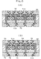
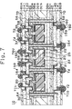
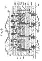
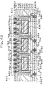
- Fig. 7 is a cross-sectional view of a printed circuit board 10 and Fig. 8 shows a state in which an IC chip 90 is mounted on the printed circuit board 10 shown in Fig. 7 and that the printed circuit board 10 is attached to a daughter board 95.
- the printed circuit board 10 consists of a core substrate 30 containing a plurality of chip capacitors 20 and buildup wiring layers 80A and 80B.
- Each of the buildup wiring layers 80A and 80B consists of a resin layer 40 and interlayer resin insulating layers 140 and 141.
- Conductor circuits 58 and via holes 60 are formed on the upper resin layer 40.
- Conductor circuits 158 and via holes 160 are formed on each of the upper and lower interlayer resin insulating layers 140.
- Conductor circuit 159 and via holes 164 are formed on each of the upper and lower interlayer resin insulating layers 141.
- Solder resist layers 70 are formed on the interlayer resin insulating layers 141, respectively.
- the buildup wiring layers 80A and 80B are connected to each other by way of through holes 56 formed in the core substrate 30.
- Each of the chip capacitors 20 consists of the first electrode 21, the second electrode 22 and a dielectric 23 put between the first and second electrodes as shown in Fig. 7.
- a plurality of pairs of first conductive films 24 connected to the first electrode 21 side and second conductive films 25 connected to the second electrode 22 side are arranged on the dielectric 23 to face one another.
- solder bumps 76U to be connected to the pads 92P1 and 92P2 of the IC chip 90 are formed on the upper buildup wiring layer 80A.
- Solder bumps 76D to be connected to the pads 94P1 and 94P2 of the daughter board 95 are formed on the lower buildup wiring layer 80B.
- the grounding pad 92P1 of the IC chip 90 is connected to the first electrode 21 of the corresponding chip capacitor 20 through the bump 76U - the conductor circuit 159 - the via hole 164 - the conductor circuit 158 - the via hole 160 - the conductor circuit 58 - the via hole 60.
- the grounding pad 94P1 of the daughter board 95 is connected to the first electrode 21 of the corresponding chip capacitor 20 through the bump 76D - the via hole 164 - the conductor circuit 158 - the via hole 160 - the through hole 56 - the conductor circuit 58 - the via hole 60.
- the power supply pad 92P2 of the IC chip 90 is connected to the second electrode 22 of the corresponding chip capacitor 20 through the bump 76U - the via hole 164 - the conductor circuit 158 - the via hole 160 - the conductor circuit 158 - the via hole 60.
- the power supply pad 94P2 of the daughter board 95 is connected to the second electrode 22 of the corresponding chip capacitor 20 through the bump 76D - the via hole 164 - the conductor circuit 158 - the via hole 160 - the through hole 56 - the via hole 60.
- Signal pads of the IC chip are, though not shown, connected to signal pads of the daughter board through the conductor circuits of the printed circuit board, the via holes and the through holes, respectively.
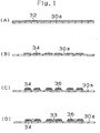
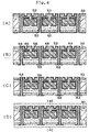
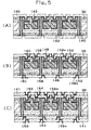
- the core substrate 30 in this embodiment consists of the first resin substrate 30a having conductive pad sections 34 for connecting the chip capacitors 20 formed on one side, the second resin substrate 30b connected to the first resin substrate 30a through a bonding resin layer (bonding plate) 38a and the third resin substrate 30c connected to the second resin substrate 30b through a bonding resin layer (bonding plate) 38b.
- An opening 30B capable of containing the chip capacitors 20 is formed in the second resin substrate 30b.
- the chip capacitors 20 can be contained in the core substrate 30. Due to this, the distance between the IC chip 90 and the chip capacitors 20 is shortened to thereby reduce the loop inductance of the printed circuit board 10. Besides, since the first resin substrate 30a, the second resin substrate 30b and the third resin substrate 30c are provided in a laminated manner, the core substrate 30 can obtain sufficient strength. Further, since the core substrate 30 is constituted smoothly by providing the first substrate 30a and the third substrate 30c on the both sides of the core substrate 30, respectively, the resin layers 40, 140 and 141 and the conductor circuits 58, 158 and 159 can be formed on the core substrate 30 appropriately and the probability of the occurrence of defective printed circuit boards can be thereby decreased.
- an insulating bonding agent 33 is interposed between the first resin substrate 30a and each chip capacitor 20.
- the coefficient of the thermal expansion of the bonding agent 33 is set lower than that of the core substrate 30, i.e., set close to that of the chip capacitors 20 made of ceramic. Due to this, even if an internal stress resulting from the difference in the coefficient of thermal expansion among the core substrate, the bonding layers 40 and the chip capacitors 20, occurs in a heat cycle test, cracks, separation and the like less occur to the core substrate, making it possible to attain high reliability. It is also possible to prevent the occurrence of migration.
- the IC chip 90 is mounted on the printed circuit board 10 thus completed so that the solder pads 92P1 and 92P2 of the IC chip 90 correspond to the solder bumps 76U of the printed circuit board 10 and a reflow process is performed, thereby attaching the IC chip 90 to the printed circuit board 10.
- a reflow process is performed so that the pads 94P1 and 94P2 of the daughter board 95 correspond to the solder bumps 76D of the printed circuit board 10, thereby attaching the printed circuit board 10 to the daughter board 95.
- the above-stated resin films contain a refractory resin, soluble particles, a hardening agent and other components, each of which will be described hereinafter.
- the resin films employed in the manufacturing method of the present invention has particles soluble in an acid or an oxidizer (to be referred to as “soluble particles” hereinafter) which particles are dispersed in a resin refractory to the acid or the oxidizer (to be referred to as “refractory resin” hereinafter).
- the soluble particles are exemplified by resin particles which are soluble in acid or an oxidizer (hereinafter called “soluble resin particles”), inorganic particles which are soluble in acid or an oxidizer (hereinafter called “inorganic soluble particles”) and metal particles which are soluble in acid or an oxidizer (hereinafter called “soluble metal particles”).
- soluble resin particles resin particles which are soluble in acid or an oxidizer
- inorganic soluble particles inorganic particles which are soluble in acid or an oxidizer
- metal particles which are soluble in acid or an oxidizer
- each of the soluble particles is not limited.
- the shape may be a spherical shape or a pulverized shape. It is preferable that the particles have a uniform shape. The reason for this lies in that a rough surface having uniformly rough pits and projections can be formed.
- the mean particle size of the soluble particles is 0.1 ⁇ m to 10 ⁇ m.
- particles having two or more particle sizes may be employed. That is, soluble particles having a mean particle size of 0.1 ⁇ m to 0.5 ⁇ m and soluble particles having a mean particle size of 1 ⁇ m to 3 ⁇ mm may be mixed. Thus, a more complicated rough surface can be formed. Moreover, the adhesiveness with the conductor circuit can be improved.
- the particle size of the soluble particles is the length of a longest portion of each of the soluble particles.
- the soluble resin particles may be particles constituted by thermosetting resin or thermoplastic resin. When the particles are immersed in solution composed of acid or an oxidizer, the particles must exhibit dissolving rate higher than that of the foregoing refractory resin.
- the soluble resin particles are exemplified by particles constituted by epoxy resin, phenol resin, phenoxy resin, polyimide resin, polyphenylene resin, polyolefin resin or fluorine resin.
- the foregoing material may be employed solely or two or more materials may be mixed.
- the soluble resin particles may be resin particles constituted by rubber.
- Rubber above is exemplified by polybutadiene rubber, a variety of denatured polybutadiene rubber, such as denatured epoxy rubber, denatured urethane rubber or denatured (metha) acrylonitrile rubber, and (metha) acrylonitrile butadiene rubber containing a carboxylic group.
- the soluble resin particles can easily be dissolved in acid or an oxidizer. That is, when the soluble resin particles are dissolved with acid, dissolution is permitted with acid except for strong acid. When the soluble resin particles are dissolved, dissolution is permitted with permanganate which has a relatively weak oxidizing power.
- chromic acid When chromic acid is employed, dissolution is permitted even at a low concentration. Therefore, retention of the acid or the oxidizer on the surface of the resin can be prevented.
- a catalyst such as palladium chloride, is supplied after the rough surface has been formed as described later, inhibition of supply of the catalyst and oxidation of the catalyst can be prevented.
- the inorganic soluble particles are exemplified by particles made of at least a material selected from a group consisting of an aluminum compound, a calcium compound, a potassium compound, a magnesium compound and a silicon compound.
- the aluminum compound is exemplified by alumina and aluminum hydroxide.
- the calcium compound is exemplified by calcium carbonate and calcium hydroxide.
- the potassium compound is exemplified by potassium carbonate.
- the magnesium compound is exemplified by magnesia, dolomite and basicmagnesium carbonate.
- the silicon compound is exemplified by silica and zeolite. The foregoing material may be employed solely or two or more materials may be mixed.
- the soluble metal particles are exemplified by particles constituted by at least one material selected from a group consisting of copper, nickel, iron, zinc, lead, gold, silver, aluminum, magnesium, potassium and silicon.
- the soluble metal particles may have surfaces coated with resin or the like in order to maintain an insulating characteristic.
- the combination of the two types of soluble particles is combination of resin particles and inorganic particles. Since each of the particles has low conductivity, an insulating characteristic with the resin film can be maintained. Moreover, the thermal expansion can easily be adjusted with the refractory resin. Thus, occurrence of a crack of the interlayer resin insulating layer constitutedby the resin film can be prevented. Thus, separation between the interlayer resin insulating layer and the conductor circuit can be prevented.
- the refractory resin is not limited when the resin is able to maintain the shape of the rough surface when the rough surface is formed on the interlayer resin insulating layer by using acid or oxidizer.
- the refractory resin is exemplified by thermosetting resin, thermoplastic resin and their composite material.
- the foregoing photosensitive resin of a type having photosensitive characteristic imparted thereto may be employed. When the photosensitive resin is employed, exposure and development processes of the interlayer resin insulating layers can be performed to form the openings for the via.
- the resin containing thermosetting resin is employed.
- the shape of the rough surface can be maintained against plating solution and when a variety of heating processes are performed.
- the refractory resin is exemplified by epoxy resin, phenol resin, phenoxy resin, polyimide resin, polyphenylene resin, polyolefin resin and fluorine resin.
- the foregoing material may be employed solely or two or more types of the materials may be mixed.
- epoxy resin having two or more epoxy groups in one molecule thereof is employed.
- the reason for this lies in that the foregoing rough surface canbe formed. Moreover, excellent heat resistance and the like can be obtained. Thus, concentration of stress onto the metal layer can be prevented even under a heat cycle condition. Thus, occurrence of separation of the metal layer can be prevented.
- the epoxy resin is exemplified by cresol novolac epoxy resin, bisphenol-A epoxy resin, bisphenol-F epoxy resin, phenol novolac epoxy resin, alkylphenol novolac epoxy resin, biphenol-F epoxy resin, naphthalene epoxy resin, dicyclopentadiene epoxy resin, an epoxy material constituted by a condensation material of phenol and an aromatic aldehyde having a phenol hydroxyl group, triglycidyl isocyanurate and alicyclic epoxy resin.
- the foregoing material may be employed solely or two or more material may be mixed. Thus, excellent heat resistance can be realized.
- the soluble particles in the resin film according to the present invention are substantially uniformly dispersed in the refractory resin.
- the reason for this lies in that a rough surface having uniform pits and projections can be formed.
- adhesiveness with the metal layer of the conductor circuit can be maintained.
- a resin film containing soluble particles in only the surface on which the rough surface is formed may be employed.
- the portions of the resin film except for the surface is not exposed to acid or the oxidizer. Therefore, the insulating characteristic between conductor circuits through the interlayer resin insulating layer can reliably be maintained.
- the amount of the soluble particles which are dispersed in the refractory resin is 3 wt% to 40 wt% with respect to the resin film.
- the amount of mixture of the soluble particles is lower than 3 wt%, the rough surface having required pits and projections cannot be formed.
- the amount is higher than 40 wt%, deep portions of the resin film are undesirably dissolved when the soluble particles are dissolved by using acid or the oxidizer.
- the insulating characteristic between the conductor circuits through the interlayer resin insulating layer constituted by the resin film cannot be maintained. Thus, short circuit is sometimes is caused to occur.
- the resin film contains a hardening agent and other components as well as the refractory resin.
- the hardening agent is exemplified by an imidazole hardening agent, an amine hardening agent, a guanidine hardening agent, an epoxy adduct of each of the foregoing hardening agents, a microcapsule of each of the foregoing hardening agents and an organic phosphine compound, such as triphenylphosphine or tetraphenyl phosphonium tetraphenyl borate.
- the content of the hardening agent is 0.05 wt% to 10 wt% with respect to the resin film.
- the content is lower than 0.05 wt%, the resin film cannot sufficiently be hardened. Thus, introduction of acid and the oxidizer into the resin film occurs greatly. In the foregoing case, the insulating characteristic of the resin film sometimes deteriorates.
- the content is higher than 10 wt%, an excessively large quantity of the hardening agent component sometimes denatures the composition of the resin. In the foregoing case, the reliability sometimes deteriorates.
- the other components are exemplified by an inorganic compound which does not exert an influence on the formation of the rough surface and a filler constituted by resin.
- the inorganic compound is exemplified by silica, alumina and dolomite.
- the resin is exemplified by polyimide resin, polyacrylic resin, polyamideimide resin, polyphenylene resin, melanine resin and olefin resin.
- the resin film may contain solvent.
- the solvent is exemplified by ketone, such as acetone, methylethylketone or cyclohexane; aromatic hydrocarbon, such as ethyl acetate, butyl acetate, cellosolve acetate, toluene or xylene.
- ketone such as acetone, methylethylketone or cyclohexane
- aromatic hydrocarbon such as ethyl acetate, butyl acetate, cellosolve acetate, toluene or xylene.
- the foregoing material may be employed solely or two or more materials may be mixed.
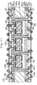
- a printed circuit board according to the first other example of the first embodiment of the present invention will be described hereinafter with reference to Fig. 9.
- the printed circuit board in the first other example of the first embodiment is almost the same as the printed circuit board in the first embodiment stated above.
- conductive connection pins 96 are provided at the printed circuit board and the printed circuit is connected to a daughter board through the conductive connection pins 96.
- chip capacitors 20 contained in the core substrate 30 are provided.
- mass storage chip capacitors 86 are mounted on the front and reverse sides of the substrate.
- the IC chip momentarily consumes high power and performs complex arithmetic operation.
- chip capacitors 20 and chip capacitors 86 for power supply are provided. The advantage derived from these chip capacitors will be described with reference to Fig. 12.
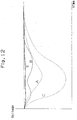
- Fig. 12 is a graph with a vertical axis indicating voltage supplied to the IC chip and a horizontal axis indicating time.
- two-dot chain line C denotes the voltage variation of a printed circuit board which is not provided with power supply capacitors. If power supply capacitors are not provided, voltage attenuates greatly.
- a broken line A denotes the voltage variation of a printed circuit board having chip capacitors mounted on the surfaces thereof. Comparedwith the two-dot chain line C, voltage does not drop greatly. However, since loop length is larger, rate-controlled power supply cannot be conducted sufficiently. Namely, at the start of the supply of power, voltage falls.
- a two-dot chain line B denotes the voltage drop of a printed circuit board including the chip capacitors described above with reference to Fig. 8. In this case, loop length can be shortened; however, mass storage chip capacitors cannot be contained in a core substrate 30 and voltage, therefore, varies.
- a solid line E denotes the voltage variation of the printed circuit board in the first other example which printed circuit board has the chip capacitors 20 mounted in the core substrate and the mass storage chip capacitors 86 mounted on the surfaces thereof. Voltage variation is minimized by providing the chip capacitors 20 and the mass storage chip capacitors 86 (having relatively high inductance) in the vicinity of the IC chip.
- the printed circuit board in the first modification is almost the same in constitution as the printed circuit board in the above-stated first embodiment.
- conductor circuits 35 are formed on one sides of the first resin substrate 30a and the third resin substrate 30c
- conductor circuits 37 are formed on the both sides of the second resin substrate 30b provided with an opening 30B for containing chip capacitors 20.
- the conductor circuits 35 are formed on one sides of the first resin substrate 30a and the third resin substrate 30c and the conductor circuits 37 are formed on the both sides of the second resin substrate 30b. Due to this, it is possible to advantageously increase wiring density and advantageously reduce the number of interlayer resin insulating layers to be built up.
- the first and second electrodes 21 and 22 are coated with copper plated films 29.
- the first and second electrodes 21 and 22 each coated with the copper plated film 29 are electrically connected to each other by a via hole 50 made of a copper plated material.
- the electrodes 21 and 22 of the chip capacitor are made bymetalization and have irregularities on the surfaces thereof.
- the first modification since the surfaces of the first and second electrodes 21 and 22 are smoothed by the copper plated films 29, no migration occurs to thereby cause no disadvantage to the electrodes of the capacitor.
- the copper plated films 29 are provided after the nickel / tin layer (coating layer) coated on the surface of each metal layer 26 in a phase of manufacturing chip capacitors 20 is separated in a phase of mounting the chip capacitors on the printed circuit board.
- the copper plated films 29 can be directly coated on the metal layers 26 in the phase of manufacturing the chip capacitors 20.
- a de-smear process is performed to thereby form via holes by copper plating. Accordingly, even if an oxide film is formed on the surface of the copper plated film 29, the oxide film can be removed by the laser and de-smear processes, thereby making it possible to establish connection appropriately.
- first and second electrodes 21 and 22 of the capacitor 20 it is also possible to employ the first and second electrodes 21 and 22 of the capacitor 20 while removing part of the coats 28 of the electrodes 21 and 22. This is because connection characteristics can be enhanced by exposing the first and second electrodes 21 and 22.
- rough layers 23 ⁇ are provided on the surfaces of a dielectric 23 of the chip capacitor 20 which dielectric is made of ceramic. Due to this, the adhesiveness between the chip capacitor 20 made of ceramic and the first resin substrate 30a made of a resin is high and the first resin substrate 30a is not separated on the interface therebetween even if a heat cycle test is conducted.
- the rough layers 23 ⁇ can be formed by polishing the surfaces of the chip capacitor 20 after sintering them or by roughing the surfaces before sintering them. In the first modification, the surfaces of the capacitor are roughed and the adhesiveness between the capacitor and the resin is thereby enhanced. Alternatively, a silane coupling process can be conducted to the surfaces of the capacitor.
- Fig. 14 is a plan view of chip capacitors.
- Fig. 14 (A) shows a chip capacitor before being cut for providing a plurality of chip capacitors.
- a dashed line denotes a cut line.
- Fig. 14(B) in the printed circuit board in the first embodiment stated above, the first electrodes 21 and the second electrodes 22 are provided on the edges of the chip capacitor.
- Fig. 14(C) shows a chip capacitor before being cut for providing a plurality of chip capacitors in the second modification.
- a dashed line denotes a cut line.
- first electrodes 21 and second electrodes 22 are provided inside of the edges of the chip capacitor.
- the chip capacitors 20 each having electrodes formed inside of the outer edges thereof are employed, so that mass storage chip capacitors can be employed.
- Fig. 15 is a plan view of a chip capacitor 20 contained in the core substrate of the printed circuit board according to the first other example.
- a plurality of small storage chip capacitors are contained in the core substrate.
- a large, mass storage chip capacitor 20 is contained in the core substrate.
- the chip capacitor 20 consists of the first electrodes 21, the second electrodes 22, a dielectric 23, first conductive films 24 connected to the first electrodes 21, second conductive films 25 connected to the second electrodes 22, electrodes 27 which are not connected to the first and second conductive films 24 and 25, for the connection of the upper and lower surfaces of the chip capacitor.
- the IC chip and the daughter board are connected to each other through the electrodes 27.
- the large chip capacitor 20 is employed in the printed circuit board in the first modification, it is possible to employ a mass storage chip capacitor. Further, since the large chip capacitor 20 is employed, the printed circuit board does not warp even if a heat cycle is performed repeatedly.
- Fig. 16(A) shows a chip capacitor before being cut for providing a plurality of chip capacitors.
- a dashed line denotes an ordinary cut line.
- Fig. 16(B) is a plan view of the chip capacitors.
- a plurality of (or in Fig. 16(B), three) chip capacitors for providing multiple capacitors are coupled to one another and employed as a large capacitor as a whole.
- the large chip capacitor 20 since the large chip capacitor 20 is employed, it is possible to employ a mass storage chip capacitor. Further, since the large chip capacitor 20 is employed, the printed circuit board does not warp even if a heat cycle is performed repeatedly.
- the chip capacitors are built in the printed circuit board.
- plate-like capacitors each constituted by providing a conductive film on a ceramic plate may be employed instead of the chip capacitors.
- the manufacturing method in the first embodiment makes it possible to contain the capacitors in the core substrate and to shorten the distance between the IC chip and the capacitors, thereby reducing the loop inductance of the printed circuit board. Further, since the printed circuit board is constituted by providing a plurality of resin layers, the core substrate can obtain sufficient strength. Besides, the first resin substrate and the third resin substrate are provided on the both sides of the core substrate, respectively, thereby constituting the core substrate smoothly. Thus, it is possible to appropriately form interlayer resin insulating layers and conductor circuits on the core substrate and to thereby decrease the probability of the occurrence of defective printed circuit boards.
- Fig. 19 is a cross-sectional view of a printed circuit board 210.
- Fig. 20 shows a state in which an IC chip 290 is mounted on the printed circuit board 210 shown in Fig. 19 and that the printed circuit board 210 is attached to a daughter board 295.
- the printed circuit board 210 consists of a core substrate 230 containing a chip capacitor 220, and buildup wiring layers 280A and 280B.
- the buildup wiring layers 280A and 280B are connected to each other by through holes 256.
- Each of the wiring layers 280A and 280B consists of interlayer resin insulating layers 240 and 340.
- conductor circuits 358 and via holes 260 connected to the first electrode 221 and the second electrode 222 of the chip capacitor 220, respectively, are formed on the interlayer resin insulating layer 240, and conductor circuits 358 and via holes 360 are formed on the interlayer resin insulating layers 340.
- conductor circuits 258 are formed on the interlayer resin insulating layer 240, and conductor circuits 358 and via holes 360 are formed on the interlayer resin insulating layer 340.
- Solder resist layers 270 are formed on the interlayer resin insulating layers 340 of the buildup wiring layers 280A and 280B, respectively.
- the chip capacitor 220 consists of the first electrode 221, the second electrode 222 and a dielectric 23 put between the first and second electrodes.
- a plurality of pairs of first conductive films 224 connected to the first electrode 221 side and second conductive film 225 connected to the second electrode 222 side are arranged to face one another.
- solder bumps 276U to be connected to the pads 292E, 292P and 292S of the IC chip 290 are provided on the upper buildup wiring layer 280A.
- Solder bumps 276D to be connected to the pads 294E, 294P and 294S of the daughter board 295 are provided on the lower buildup wiring layer 280B.
- the signal pads 292S of the IC chip 290 shown in Fig. 20 are connected to the signal pads 294S of the daughter board 295 through the bumps 276U - the conductor circuits 358 - the via holes 360 - the through holes 256 - the via holes 360 - the bumps 276D, respectively.
- the grounding pad 292E of the IC chip 290 is connected to the first electrode 221 of the chip capacitor 220 through the bump 276U - the via hole 360 - the conductor circuit 258 - the via hole 260.
- the grounding pad 294E of the daughter board 295 is connected to the first electrode 221 of the chip capacitor 220 through the bump 276D - the via hole 360 - the through hole 256 - the via hole 260.
- the power supply pad 292P of the IC chip is connected to the second electrode 222 of the chip capacitor 220 through the bump 276U - the via hole 360 - the conductor circuit 258 - the via hole 260.
- the power supply pad 294P of the daughter board 295 is connected to the second electrode 222 of the chip capacitor 220 through the bump 276D - the via hole 360 - the through hole 256 - the via hole 260.
- the core substrate 230 in this embodiment consists of the first resin substrate 230a, the second resin substrate 230b connected to the first resin substrate 230a through a bonding resin layer (bonding plate) 238a and the third resin substrate 230c connected to the second resin substrate 230b through a bonding resin layer (bonding plate) 238b.
- Conductor circuits 235 are formed on the both sides of the first resin substrate 230a, the second resin substrate 230b and the third resin substrate 230c.
- a concave portion 334 capable of containing the chip capacitor 220 is formed in the core substrate 230 by spot facing and the chip capacitor 220 is contained in the concave portion 334.
- the chip capacitor 220 can be contained in the core substrate 230, so that the distance between the IC chip 290 and the chip capacitor 220 becomes short and the loop inductance of the printed circuit board 210 can be reduced. Further, since the core substrate 230 is formed by providing the first, second and third resin substrates 230a, 230b and 230c each having the conductor circuits 235 arranged on the both sides thereof, wiring density within the core substrate 230 increases and the number of interlayer resin insulating layers can be thereby reduced.
- an bonding agent 236 is interposed between the lower surface of the through hole 34 of the core substrate 230 and the chip capacitor 220, and resin filler 233 is filled between the side surface of the through hole 237 and the chip capacitor 220.
- the coefficients of thermal expansion of the bonding agent 236 and the resin filler 233 are set lower than that of the core substrate 230, i.e., set close to that of the chip capacitor 220 made of ceramic. Due to this, even if an internal stress resulting from the difference in the coefficient of thermal expansion occurs between the core substrate 230 and the chip capacitor 220, cracks, separation and the like less occur to the core substrate 230 and high reliability can be, therefore, attained. It is also possible to prevent the occurrence of migration.
- the IC chip 290 is mounted on the printed circuit board 210 thus completed so that the solder pads 292E, 292P and 292S of the IC chip 290 correspond to the solder bumps 276U of the printed circuit board 210 and a reflow process is performed, thereby attaching the IC chip 290 to the printed circuit board 210.
- a reflow process is performed so that the pads 294E, 294P and 294S of the daughter board 295 correspond to the solder bumps 276D of the printed circuit board 210, thereby attaching the printed circuit board 210 to the daughter board 295.
- thermosetting epoxy resin sheets forming the above-stated interlayer resin insulating layers 240 and 340 each contain a refractory resin, soluble particles, a hardening agent and other components, each of which is the same as that in the first embodiment already described above and will not be described herein.
- a printed circuit board 212 according to the first modification of the second embodiment of the present invention will be described with reference to Fig. 23.
- a BGA ball grid array
- the printed circuit board in the first modification of the second embodiment is constituted into a PGA system for establishing connection through conductive connection pins 296 as shown in Fig. 23.
- the concave portion 334 for containing the chip capacitor 220 is provided in the core substrate 230 by spot facing to allow the chip capacitor 220 to be contained in the concave portion 334.
- the first resin substrate 230a provided with through holes 230A, the second and third resin substrates 230b and 230c which are not provided with through holes are bonded to one another through bonding resin layers (bonding plates) 238a and 238b, thereby forming a core substrate 230 provided with a concave portion 335 containing chip capacitors 220 to allow a plurality of chip capacitors 220 to be contained in the concave portion 335.
- a printed circuit board according to the first other example of the first modification of the second embodiment of the present invention will be described with reference to Fig. 24.
- the printed circuit board in the first other example is almost the same as that in the first modification of the second embodiment stated above.
- only the chip capacitors 220 contained in the core substrate 230 are provided in the first modification of the second embodiment, whereas mass storage chip capacitors 286 are mounted on the front and reverse sides of a core substrate in the first other example.
- Fig. 12 is a graph with a vertical axis indicating voltage supplied to the IC chip and a horizontal axis indicating time.
- two-dot chain line C denotes the voltage variation of a printed circuit board which is not provided with power supply capacitors. If power supply capacitors are not provided, voltage attenuates greatly.
- a broken line A denotes the voltage variation of a printed circuit board having chip capacitors mounted on the surfaces thereof. Compared with the two-dot chain line C, voltage does not drop greatly. However, since loop length is larger, rate-controlled power supply cannot be conducted sufficiently. Namely, at the start of the supply of power, voltage falls.
- a two-dot chain line B denotes the voltage drop of a printed circuit board including the chip capacitors described above with reference to Fig. 23.
- loop length can be shortened; however, mass storage chip capacitors cannot be contained in a core substrate 230 and voltage, therefore, varies.
- a solid line E denotes the voltage variation of the printed circuit board in the modification which printed circuit board has the chip capacitors 220 mounted in the core substrate and the mass storage chip capacitors 286 mounted on the surfaces thereof. Voltage variation is minimized by providing the chip capacitors 220 and the mass storage chip capacitors 286 (having relatively high inductance) in the vicinity of the IC chip.
- the first and second electrodes 221 and 222 are coated with copper plated films 29.
- the first and second electrodes 221 and 222 each coated with the copper plated film 29 are electrically connected to each other by a via hole 260 made of a copper plated material.
- the electrodes 221 and 222 of the chip capacitor are made by metalization and have irregular portions on the surfaces thereof.
- the via holes 260 are formed by plating in the electrodes 221 and 222 having the copper plated films 29 formed thereon, respectively, the connection characteristics between the electrodes 221, 222 and the via holes 260 is good and disconnection does not occur between the electrodes 221, 222 and the via holes 260 even if a heat cycle test is conducted. Besides, no migration occurs and no disadvantages are derived in the connection portions of the via holes of the capacitors.
- the copper plated films 29 are provided after the nickel / tin layer (coating layer) coated on the surface of each metal layer 26 in a phase of manufacturing chip capacitors is separated in a phase of mounting the chip capacitors on the printed circuit board.
- the copper plated films 29 can be directly coated on the metal layers 26 in the phase of manufacturing the chip capacitors 220.
- a de-smear process is performed to thereby form via holes by copper plating. Accordingly, even if an oxide film is formed on the surface of the copper plated film 29, the oxide film can be removed by the laser and de-smear processes, thereby making it possible to establish connection appropriately.
- rough layers 23 ⁇ are provided on the surfaces of a dielectric 23 of the chip capacitors 220 which dielectric is made of ceramic. Due to this, the adhesiveness between the chip capacitors 220 made of ceramic and the interlayer resin insulating layer 240 made of a resin is high and the interlayer resin insulating layer 240 is not separated on the interface therebetween even if a heat cycle test is conducted.
- the rough layers 23 ⁇ can be formed by polishing the surfaces of the chip capacitors 220 after sintering them or by roughing the surfaces before sintering them. In the first other example, the surfaces of the capacitors are roughed and the adhesiveness between the capacitors and the resin is thereby enhanced. Alternatively, a silane coupling process can be conducted to the surfaces of the capacitors.
- first and second electrodes 21 and 22 of the first and second capacitors 220 it is also possible to employ the first and second electrodes 21 and 22 of the first and second capacitors 220 while removing part of the coats 28 of the electrodes 21 and 22. This is because connection characteristics can be enhanced by exposing the first and second electrodes 221 and 222.
- Fig. 14 is a plan view of chip capacitors.
- Fig. 14(A) shows a chip capacitor before being cut for providing a plurality of chip capacitors.
- a dashed line denotes a cut line.
- Fig. 14(B) in the printed circuit board in the first embodiment stated above, the first electrodes 21 and the second electrodes 22 are provided on the edges of the chip capacitor.
- Fig. 14(C) shows a chip capacitor before being cut for providing a plurality of chip capacitors in the second modification.
- a dashed line denotes a cut line.
- first electrodes 21 and second electrodes 22 are provided inside of the edges of the chip capacitor.
- the chip capacitors 20 each having electrodes formed inside of the outer edges thereof are employed, so that mass storage chip capacitors can be employed.
- Fig. 15 is a plan view of a chip capacitor 20 contained in the core substrate of the printed circuit board according to the first other example.
- a plurality of small storage chip capacitors are contained in the core substrate.
- a large, mass storage chip capacitor 20 is contained in the core substrate.
- the chip capacitor 20 consists of the first electrodes 21, the second electrodes 22, a dielectric 23, first conductive films 24 connected to the first electrodes 21, second conductive films 25 connected to the second electrodes 22, and electrodes 27 which are not connected to the first and second conductive films 24 and 25, for the connection of the upper and lower surfaces of the chip capacitor.
- the IC chip and the daughter board are connected to each other through the electrodes 27.
- the large chip capacitor 20 is employed in the printed circuit board in the first modification, it is possible to employ a mass storage chip capacitor. Further, since the large chip capacitor 20 is employed, the printed circuit board does not warp even if a heat cycle is performed repeatedly.
- Fig. 16(A) shows a chip capacitor before being cut for providing a plurality of chip capacitors.
- a dashed line denotes an ordinary cut line.
- Fig. 16(B) is a plan view of the chip capacitors.
- a plurality of (or in Fig. 16(B), three) chip capacitors for providing multiple capacitors are coupled to one another and employed as a large capacitor as a whole.
- the large chip capacitor 20 since the large chip capacitor 20 is employed, it is possible to employ a mass storage chip capacitor. Further, since the large chip capacitor is employed, the printed circuit board does not warp even if a heat cycle is performed repeatedly.
- the chip capacitors are built in the printed circuit board.
- plate-like capacitors each constituted by providing a conductive film on a ceramic plate may be employed instead of the chip capacitors.
- the second embodiment it is possible to contain the capacitors in the core substrate and to shorten the distance between the IC chip and the capacitors, thereby reducing the loop inductance of the printed circuit board. Further, since the core substrate is formed by providing a plurality of resin substrates having conductor circuits formed thereon in a multilayer manner, the wiring density within the core substrate is increased and the number of interlayer resin insulating layers can be reduced.
- Fig. 30 is a cross-sectional view of a printed circuit board 410.
- Fig. 31 shows a state in which an IC chip 490 is mounted on the printed circuit board 410 shown in Fig. 30 and that the printed circuit board 410 is attached to a daughter board 495.
- the printed circuit board 410 consists of a core substrate 430 containing a plurality of chip capacitors 420, and buildup wiring layers 480A and 480B.
- Each of the buildup wiring layers 480A and 480B consists of interlayer resin insulating layers 540 and 541.
- Conductor circuits 558 and via holes 560 are formed on the interlayer resin insulating layer 540 of each of the buildup wiring layers 480A and 480B.
- Conductor circuits 559 and via holes 564 are formed on the interlayer rein insulating layer 541 of each of the buildup wiring layers 480A and 480B.
- Solder resist layers 470 are formed on the interlayer resin insulating layers 541, respectively. Via holes 460 and conductor circuits 458 to be connected to the chip capacitors 420 are provided on the core substrate 430.
- the buildup wiring layers 480A and 480B are connected to each other by way of through holes 456 formed in the core substrate 430.
- each of the chip capacitors 420 consists of the first electrode 421, the second electrode 422 and a dielectric 423 put between the first and second electrodes.
- a plurality of pairs of first conductive films 424 connected to the first electrode 421 side and second conductive films 425 connected to the second electrode 422 side are arranged on the dielectric 423 to face one another.
- solder bumps 476U to be connected to the pads 492E, 492P and 492S of the IC chip 490 are provided on the upper buildup wiring layer 480A.
- Solder bumps 476D to be connected to the pads 494E1, 494E2, 494P1, 494P2 and 494S of the daughter board 495 are provided on the lower buildup wiring layer 480B.
- the signal pad 492S of the IC chip 490 is connected to the signal pad 494S of the daughter board 495 through the bump 476U - the conductor circuit 559 - the via hole 564 - the conductor circuit 558 - the via hole 560 - the through hole 456 - the via hole 560 - the conductor circuit 558 - the via hole 564 - the conductor circuit 559 - the bump 476D.
- the grounding pad 492E of the IC chip 490 is connected to the first electrodes 421 of the chip capacitors 420 through the bumps 476U - the via holes 564 - the conductor circuits 558 - the via holes 560 - the conductor circuits 458 - the via holes 460.
- the grounding pad 494E1 of the daughter board 495 is connected to the first electrodes 421 of the chip capacitors 420 through the bumps 476D - the via holes 564 - the conductor circuits 558 - the via holes 560 - the through holes 456 - the conductor circuits 458 - the via holes 460.
- the grounding pad 494E2 is connected to the first electrodes 421 of the chip capacitors 420 through the bumps 476D - the via holes 564 - the conductor circuits 558 - the via holes 560 - the conductor circuits 458 - the via holes 460.
- the power supply pad 492P of the IC chip 490 is connected to the second electrodes 422 of the chip capacitors 420 through the bumps 476U - the via holes 564 - the conductor circuits 558 - the via holes 560 - the conductor circuits 458 - the via holes 460.
- the power supply pad 494P1 of the daughter board 495 is connected to the second electrodes 422 of the chip capacitors 420 through the bumps 476D - the via holes 564 - the conductor circuits 558 - the via holes 560 - the through holes 456 - the conductor circuits 458 - the via holes 460.
- the power supply pad 494P2 is connected to the first electrodes 422 of the chip capacitors 420 through the bumps 476D - the via holes 564 - the conductor circuits 558 - the via holes 560 - the conductor circuits 458 - the via holes 460.
- the daughter board 495 side is connected to the first and second electrodes 421 and 422 of the chip capacitors 420 through the through holes 456. It is also possible to connect the daughter board 495 side thereto without employing the through holes.
- the core substrate 430 in this embodiment consists of the first resin substrate 430a to which the chip capacitors 420 are connected through bonding materials, the second resin substrate 430b connected to the first resin substrate 430a through a bonding resin layer (bonding plate) 438a and the third resin substrate 430c connected to the second resin substrate 430b through a bonding resin layer (bonding plate) 438b.
- An opening 430B capable of containing the chip capacitors 420 are formed in the second resin substrate 430b.
- the chip capacitors 420 can be contained in the core substrate 430, so that the distance between the IC chip 490 and each chip capacitor 420 is shortened and the loop inductance of the printed circuit board 410 can be reduced.
- the core substrate 430 is constituted by providing the first resin substrate 430a, the second resin substrate 430b and the third resin substrate 430c in a multilayer manner, the core substrate 430 can obtain sufficient strength.
- the core substrate 430 is constituted smoothly by providing the first resin substrate 430a and the third resin substrate 430c on the both sides of the core substrate 430, respectively, it is possible to appropriately form the interlayer resin insulating layers 540, 541, the conductor circuits 558, 559 and the via holes 560 and 564 on the core substrate 430 and the probability of the occurrence of defective printed circuit boards can be decreased.
- the via holes 460 are provided on the both sides of the core substrate 430. This makes it possible to connect the daughter board 495 to each chip capacitors 420 at the shortest distance and high electric power can be supplied momentarily from the daughter board to the IC chip.
- an insulating bonding agent 436 is interposed between the first resin substrate 430a and each of the chip capacitors 420.
- the coefficient of the thermal expansion of the bonding agent 436 is set lower than that of the core substrate 430, i.e., set close to that of the chip capacitors 420 made of ceramic. Due to this, even if an internal stress resulting from the difference in the coefficient of thermal expansion among the core substrate, the bonding layers 436 and the chip capacitors 420, occurs in a heat cycle test, cracks, separation and the like less occur to the core substrate, making it possible to attain high reliability. It is also possible to prevent the occurrence of migration.
- a printed circuit board according to the first other example of the third embodiment of the present invention will be described hereinafter with reference to Fig. 32.
- the printed circuit board in the first other example is almost the same as the printed circuit board in the third embodiment stated above.
- conductive connection pins 496 are provided at the printed circuit board and the printed circuit is connected to a daughter board through the conductive connection pins 496.
- chip capacitors 420 contained in the core substrate 430 are provided.
- mass storage chip capacitors 486 are mounted on the front and reverse sides of the substrate.
- the IC chip momentarily consumes high power and performs complex arithmetic operation.
- chip capacitors 420 and chip capacitors 486 for power supply are provided. The advantage derived from these chip capacitors will be described with reference to Fig. 12.
- Fig. 12 is a graph with a vertical axis indicating voltage supplied to the IC chip and a horizontal axis indicating time.
- two-dot chain line C denotes the voltage variation of a printed circuit board which is not provided with power supply capacitors. If power supply capacitors are not provided, voltage attenuates greatly.
- a broken line A denotes the voltage variation of a printed circuit board having chip capacitors mounted on the surfaces thereof. Compared with the two-dot chain line C, voltage does not drop greatly. However, since loop length is larger, rate-controlled power supply cannot be conducted sufficiently. Namely, at the start of the supply of power, voltage falls.
- a two-dot chain line B denotes the voltage drop of a printed circuit board including the chip capacitors described above with reference to Fig. 31. In this case, loop length can be shortened; however, mass storage chip capacitors cannot be contained in a core substrate 430 and voltage, therefore, varies.
- a solid line E denotes the voltage variation of the printed circuit board in the first other example which printed circuit board has the chip capacitors 420 mounted in the core substrate and the mass storage chip capacitors 486 mounted on the surfaces thereof. Voltage variation is minimized by providing the chip capacitors 420 and the mass storage chip capacitors 486 (having relatively high inductance) in the vicinity of the IC chip.
- each conductor circuit 458 consists of three layers, i.e., the copper foil 432, the Ni-Cu metal layer 448 and the electroplated film 452.
- each conductor circuit 458 consists of two layers, i.e., an electroless plated film 443 and an electroplated film 452. Namely, the copper foil 432 is removed and thickness is reduced, thereby forming the conductor circuit 458 at fine pitch.
- conductor circuits 435 are formed on the both sides of the second resin substrate 430b provided with an opening 430B for containing chip capacitors 420.
- the conductor circuits 435 are formed on the both sides of the second resin substrate 430b provided with the opening 430B for containing the chip capacitors 420, it is possible to increase wiring density within the core substrate 430 and to reduce the number of interlayer resin insulating layers to be built up.
- the first and second electrodes 421 and 422 are coated with copper plated films 29.
- the first and second electrodes 421 and 422 each coated with the copper plated film 29 are electrically connected to each other by via holes 460 made of a copper plated material.
- the electrodes 421 and 422 of the chip capacitor are made by metalization and have irregular portions on the surfaces thereof.
- the resin may sometimes remain on the irregular portions in the step of providing non-penetrating holes 442 in the first resin substrate 430a. At this time, the resin residue causes connection defects between the first, second electrodes 421, 422 and the via holes 460.
- the first modification of the third embodiment since the surfaces of the first and second electrodes 421 and 422 are smoothed by the copper plated films 29, no resin remains when providing openings 442 in the coated first resin substrate 430a on the electrodes and the reliability of the connection between the electrodes 421, 422 and the via holes 460 when forming the via holes 460 can be enhanced.
- the via holes 460 are formed by plating in the electrodes 421 and 422 having the copper plated films 29 formed thereon, respectively, the connection characteristic between the electrodes 421, 422 and the via holes 460 is good and disconnection does not occur between the electrodes 421, 422 and the via holes 460 even if a heat cycle test is conducted. Besides, no migration occurs and no disadvantages are derived in the connection section of the via holes of the capacitors.
- the copper plated films 29 are provided after the nickel / tin layer (coating layer) coated on the surface of each metal layer 26 in a phase of manufacturing chip capacitors is separated in a phase of mounting the chip capacitors on the printed circuit board.
- the copperplated films 29 can be directly coated on the metal layers 26 in the phase of manufacturing the chip capacitors 420.
- a de-smear process is performed to thereby form via holes by copper plating. Accordingly, even if an oxide film is formed on the surface of the copper plated film 29, the oxide film can be removed by the laser and de-smear processes, thereby making it possible to establish connection appropriately.
- rough layers 23a are provided on the surfaces of a dielectric 423 of each chip capacitor 420 which dielectric is made of ceramic. Due to this, the adhesiveness between the chip capacitors 420 made of ceramic and the resin substrates 438a and 438bmade of a resin is high and the first resin substrate 430a is not separated on the interface therebetween even if a heat cycle test is conducted.
- the rough layers 23a can be formed by polishing the surfaces of the chip capacitors 420 after sintering them or by roughing the surfaces before sintering them. In the first modification of the third embodiment, the surfaces of the capacitors are roughed and the adhesiveness between the capacitors and the resin is thereby enhanced. Alternatively, a silane coupling process can be conducted to the surfaces of the capacitors.
- first and second electrodes 21 and 22 of the capacitors 420 it is also possible to employ the first and second electrodes 21 and 22 of the capacitors 420 while removing part of the coats 28 of the electrodes 21 and 22. This is because connect ion characteristics can be enhanced by exposing the first and second electrodes 21 and 22.
- the via holes are provided on the both sides of the core substrate. It is also possible to form via holes only on one side of the substrate. Further, the openings 432a of the copper foils 432 on the surfaces of the core substrate 430 are employed as conformal masks in this modification. It is also possible to provide openings reaching the capacitors by applying laser without employing the conformal masks of the core substrate 430.
- Fig. 14 is a plan view of chip capacitors.
- Fig. 14 (A) shows a chip capacitor before being cut for providing a plurality of chip capacitors.
- a dashed line denotes a cut line.
- Fig. 14(B) in the printed circuit board in the first embodiment stated above, the first electrodes 21 and the second electrodes 22 are provided on the edges of the chip capacitor.
- Fig. 14 (C) shows a chip capacitor before being cut for providing a plurality of chip capacitors in the second modification.
- a dashed line denotes a cut line.
- first electrodes 21 and second electrodes 22 are provided inside of the edges of the chip capacitor.
- the chip capacitors 20 each having electrodes formed inside of the outer edges thereof are employed, so that mass storage chip capacitors can be employed.
- Fig. 15 is a plan view of a chip capacitor 20 contained in the core substrate of the printed circuit board according to the first other example.
- a plurality of small storage chip capacitors are contained in the core substrate.
- a large, mass storage chip capacitor 20 is contained in the core substrate.
- the chip capacitor 20 consists of the first electrodes 21, the second electrodes 22, a dielectric 23, the first conductive films 24 connected to the first electrodes 21, the second conductive films 25 connected to the second electrodes 22, electrodes 27 which are not connected to the first and second conductive films 24 and 25, for the connection of the upper and lower surfaces of the chip capacitor.
- the IC chip and the daughter board are connected to each other through the electrodes 27.
- the large chip capacitor is employed in the printed circuit board in the first modification, it is possible to employ a mass storage chip capacitor. Further, since the large chip capacitor 20 is employed, the printed circuit board does not warp even if a heat cycle is performed repeatedly.
- Fig. 16(A) shows a chip capacitor before being cut for providing a plurality of chip capacitors.
- a dashed line denotes an ordinary cut line.
- Fig. 16 (B) is a plan view of the chip capacitors.
- a plurality of (or in Fig. 16(B), three) chip capacitors for providing multiple capacitors are coupled to one another and employed as a large capacitor as a whole.
- the large chip capacitor 20 since the large chip capacitor 20 is employed, it is possible to employ a mass storage chip capacitor. Further, since the large chip capacitor 20 is employed, the printed circuit board does not warp even if a heat cycle is performed repeatedly.
- the chip capacitors are built in the printed circuit board.
- plate-like capacitors each constituted by providing a conductive film on a ceramic plate may be employed instead of the chip capacitors.
- the structure of the third embodiment makes it possible to contain the capacitors in the core substrate and to shorten the distance between the IC chip and each capacitor, thereby reducing the loop inductance of the printed circuit board. Further, since the printed circuit board is constituted by providing resin substrates in a multilayer manner, the core substrate can obtain sufficient strength. Besides, the first resin substrate and the third resin substrate are provided on the both sides of the core substrate, respectively, thereby constituting the core substrate smoothly. Thus, it is possible to appropriately form interlayer resin insulating layers and conductor circuits on the core substrate and to thereby decrease the probability of the occurrence of defective printed circuit boards.
- the opening diameters of the via holes depend on the opening diameters of the openings of metal films, so that it is possible to form each viahole to have an appropriate diameter.
- the positional accuracy of the via hole openings depend on the opening positions of the openings of the metal films, so that it is possible to form the via holes at appropriate positions even if the positional accuracy of the laser application is low.
- the structure allows reducing the loop inductance and increasing the degree of freedom for arrangement.
- Fig. 42 is a cross-sectional view of a printed circuit board 610.
- Fig. 43 shows a state in which an IC chip 690 is mounted on the printed circuit board 610 shown in Fig. 42 and that the printed circuit board 610 is attached to a daughter board 694.
- Fig. 44(A) is an enlarged view of a via hole 660 shown in Fig. 42.
- Fig. 44(B) is a typical view showing a state in which a plurality of via holes 760 are provided in the via hole 660 shown in Fig. 44(A), which view is seen from an arrow B side.
- the printed circuit board 610 consists of a core substrate 630 containing a plurality of chip capacitors 620, and buildup wiring layers 680A and 680B. Relatively large via holes 660 are connected to the electrodes 621 and 622 of the plural chip capacitors 620 contained in the core substrate 630.
- Each of the buildup wiring layers 680A and 680B consists of interlayer resin insulating layers 740 and 741. Conductor circuits 758 and relatively small via holes 760 are formed on the interlayer resin insulating layers 740, whereas conductor circuits 759 and relatively small via holes 764 are formed on the interlayer resin insulating layers 741. Solder resist layers 670 are provided on the interlayer resin insulating layers 741, respectively.
- each of the chip capacitors 620 consists of the first electrode 621, the second electrode 622 and a dielectric 23 put between the first and second electrodes.
- a plurality of pairs of the first conductive films 24 connected to the first electrode 621 side and the second conductive films 25 connected to the second electrode 622 side are arranged on the dielectric 23 to face one another.
- part of coats 28 of the first electrodes 21 and the second electrodes 22 of the capacitors 620 can be removed. This is because the connection characteristics with respect to the via holes made by plating can be enhanced by exposing the first and second electrodes 21 and 22.
- solder bumps 676U to be connected to the pads 692 of the IC chip 690 are formed on the via hole 764 of the upper buildup wiring layer 680A.
- Solder bumps 676D to be connected to the pads 694 of the daughter board 695 are formed on the via holes 764 of the lower buildup wiring layer 680B.
- a resin substrate is employed as the core substrate.
- a resin material used for an ordinary printed circuit board such as a glass epoxy resin impregnated material, a phenol resin impregnated material or the like can be employed.
- substrates made of ceramic or AIN cannot employed as the core substrate. This is because such a substrate has poor workability for the outside shape thereof, sometimes cannot contain capacitors and has gaps even if filled with a resin.
- a plurality of chip capacitors 620 are contained in a concave portion 734 formed in the core substrate, so that it is possible to arrange the chip capacitors 620 with high density. Further, since a plurality of chip capacitors 620 are contained in the concave portion 734, it is possible to make the heights of the chip capacitors 620 uniform. Due to this, the thicknesses of the resin layers 640 on the chip capacitors 620 can be made uniform, so that it is possible to appropriately form via holes 660. Besides, since the distance between the IC chip 690 and each chip capacitor 620 becomes shorter, so that it is possible to reduce loop inductance.
- a plurality of via holes 760 in the upper buildup wiring layer 680A are connected to one via hole 660.
- the large via hole 660 as shown in Fig. 44(B) is formed to have an inside diameter of 125 ⁇ m and a land diameter of 165 ⁇ m
- the small via hole 760 is formed to have an inside diameter of 25 ⁇ m and a land diameter of 65 ⁇ m.
- the chip capacitors 620 are formed rectangularly and the first and the first electrode 621 and the second electrode 621 of each capacitor are formed rectangularly to have one side of 250 ⁇ m.
- the via holes 660 are formed as filled via holes filled with a plated material and having flat surfaces. This makes it possible to directly connect a plurality of via holes 760 onto the via hole 660. Thus, it is possible to enhance the characteristics of the connection between the via holes 660 and 760 and to ensure the supply of power from the chip capacitors 620 to the IC chip 690.
- the filled via holes are formed by filling a plated material within the holes. It is also possible to employ filled via holes each having a metal film provided on the front surface after filling a resin in the holes.
- the coefficients of thermal expansion of resin filler 633 and a bonding material 636 below the chip capacitors 620 are set lower than those of the core substrate 630 and resin insulating layers 640, i.e., set close to those of the chip capacitors 620 made of ceramic. Due to this, even if an internal stress resulting from difference in the coefficient of thermal expansion occurs among the core substrate 630, the resin insulating layers 640 and the chip capacitors 620 during a heat cycle test, cracks, separation and the like less occurs to the core substrate 630 and the resin insulating layers 640, thereby making it possible to attain high reliability.
- a copper plated film 29 is coated on the surface of a metal layer 26 constituting the first electrode 621 and the second electrode 622.
- the plated film coat is formed by plating such as electroplating and electroless plating.
- the first and second electrodes 621 and 622 coated with the copper plated films 29 are electrically connected to the via holes 660 made of a copper plated material.
- the electrodes 621 and 622 of the chip capacitors are formed by metalization and have irregular portions on the surfaces thereof.
- the via holes 660 are formed by plating in the electrodes 621 and 622 having the copper plated films 29 formed thereon, respectively, the characteristic of the connection between the electrodes 621, 622 and the via holes 660 is high and disconnection does not occur between the electrodes 621, 622 and the via holes 660 even if a heat cycle test is conducted.
- the copper plated films 29 are provided after the nickel / tin layer (coating layer) coated on the surface of each metal layer 26 in a phase of manufacturing chip capacitors is separated in a phase of mounting the chip capacitors on the printed circuit board.
- the copper plated films 29 can be directly coated on the metal layers 26 in the phase of manufacturing the chip capacitors 220. Namely, in this embodiment, after openings reaching the copper plated films 29 of the electrodes are provided by applying laser, a de-smear process is performed to thereby form via holes by copper plating. Accordingly, even if an oxide film is formed on the surface of the copper plated film 29, the oxide film can be removed by the laser and de-smear processes, thereby making it possible to establish connection appropriately.
- rough layers 23 ⁇ may be provided on the surfaces of the dielectrics 23 of the chip capacitors 620 which dielectrics are made of ceramic. By doing so, the adhesiveness between the chip capacitors 620 made of ceramic and the interlayer resin insulating layer 640 made of a resin is high and the interlayer resin insulating layer 640 is not separated on the interface therebetween even if a heat cycle test is conducted.
- the rough layers 23 ⁇ can be formed by polishing the surfaces of the chip capacitors 620 after sintering them or by roughing the surfaces before sintering them. In this embodiment, the surfaces of the capacitors are roughed and the adhesiveness between each capacitor and the resin is thereby enhanced.
- a silane coupling process can be conducted to the surfaces of the capacitors.
- the IC chip 690 is mounted on the printed circuit board 610 thus completed so that the solder pads 692 of the IC chip 690 correspond to the solder bumps 676U of the printed circuit board 610 and a reflow process is performed, thereby mounting the IC chip 690 on the printed circuit board 610.
- a reflow process is performed so that the pads 694 of the daughter board 695 correspond to the solder bumps 676D of the printed circuit board 610, thereby attaching the printed circuit board 610 to the daughter board 695.
- the above-stated resin contains a refractory resin, soluble particles, a hardening agent and other components, each of which is the same as that described in the first embodiment and will not be described herein.
- a printed circuit board 612 according to the first modification of the fourth embodiment of the present invention will be described with reference to Fig. 52.
- the first modification of the fourth embodiment is almost the same as the fourth embodiment.
- the printed circuit board in this modification is constituted into a PGA system establishing connection through conductive connection pins 696.
- the IC chip 690 is mounted on the printed circuit board 612 so that the solder pads 692 of the IC chip 690 correspond to the opening 671U side-solder bumps 676U of the printed circuit board 612, and a reflow process is performed, thereby attaching the IC chip 690 (Fig. 53).
- a printed circuit board according to the second modification of the fourth embodiment of the present invention will be described with reference to Fig. 53.
- a printed circuit board 614 in the second modification of the fourth embodiment is almost the same as that in the fourth embodiment stated above.
- one chip capacitor 620 is contained in the concave portion 736 formed in the core substrate 630. Since the chip capacitor 620 is arranged within the core substrate 630, the distance between the IC chip 690 and the chip capacitor 620 becomes short and loop inductance can be reduced.
- Fig. 14 is a plan view of chip capacitors.
- Fig. 14(A) shows a chip capacitor before being cut for providing a plurality of chip capacitors.
- a dashed line denotes a cut line.
- Fig. 14(B) in the printed circuit board in the first embodiment stated above, the first electrodes 21 and the second electrodes 22 are provided on the edges of the chip capacitor.
- Fig. 14 (C) shows a chip capacitor before being cut for providing a plurality of chip capacitors in the third modification.
- a dashed line denotes a cut line.
- first electrodes 21 and second electrodes 22 are provided inside of the edges of the chip capacitor.
- the chip capacitors 20 each having electrodes formed inside of the outer edges thereof are employed, so that mass storage chip capacitors can be employed.
- Fig. 15 is a plan view of a chip capacitor 20 contained in the core substrate of the printed circuit board according to the first other example.
- a plurality of small storage chip capacitors are contained in the core substrate.
- a large, mass storage chip capacitor 20 is contained.
- the chip capacitor 20 consists of the first electrodes 21, the second electrodes 22, a dielectric 23, first conductive films 24 connected to the first electrodes 21, second conductive films 25 connected to the second electrodes 22, electrodes 27 which are not connected to the first and second conductive films 24 and 25, for the connection of the upper and lower surfaces of the chip capacitor.
- the IC chip and the daughter board are connected to each other through the electrodes 27.
- the large chip capacitor is employed in the printed circuit board in the first modification, it is possible to employ a mass storage chip capacitor. Further, since the large chip capacitor 20 is employed, the printed circuit board does not warp even if a heat cycle is performed repeatedly.
- FIG. 16 (A) shows a chip capacitor before being cut for providing a plurality of chip capacitors.
- a dashed line denotes an ordinary cut line.
- Fig. 16(B) is a plan view of the chip capacitors.
- a plurality of (or in Fig. 16(B), three) chip capacitors for providing multiple capacitors are coupled to one another and employed as a large capacitor as a whole.
- the large chip capacitor 20 since the large chip capacitor 20 is employed, it is possible to employ a mass storage chip capacitor. Further, since the large chip capacitor is employed, the printed circuit board does not warp even if a heat cycle is performed repeatedly.
- the chip capacitors are built in the printed circuit board.
- plate-like capacitors each constituted by providing a conductive film on a ceramic plate may be employed instead of the chip capacitors.
- voltage variation can be minimized by providing the chip capacitors 20 in the vicinity of the IC chip and the mass storage chip capacitors (having relatively high inductance) on the front and reverse sides.
- the measurement values of the inductance of the chip capacitor 620 embedded in the core substrate and that of the chip capacitor mounted on the reverse side (daughter board side-surface) of the printed circuit board are shown below.
- Rate of Change of Capacitance (measurement frequency 100Hz) (measurement frequency 1kHz) Steam 168 hours 0.3% 0.4% HAST 100 hours -0.9% -0.9% TS 1000 cycles 1.1% 1.3%
- the printed circuit board including the chip capacitor(s) therein can attain equivalent reliability to that of the existing capacitor surface mount type.
- the TS test it was discovered that even if an internal stress occurs due to the difference in the coefficient of thermal expansion among the capacitors made of ceramic, the core substrate made of a resin and the interlayer resin insulating layers, disconnection does not occur between the electrodes of the chip capacitors and the via holes, separation does not occur between the chip capacitors and the interlayer resin insulating layers and cracks do not occur to the interlayer resin insulating layer, whereby high reliability can be attained for a long time.
- the via holes in the fourth embodiment are formed between the conductor circuits and the capacitors. Due to this, it is possible to maintain desired performance without delaying operation due to lack of power supply and no problems arose even if a reliability test was conducted.
- the via holes because of the via holes, even if the via holes are formed in the interlayer resin insulating layers and positional errors occur to the via holes, the allowance is wide. Thus, electrical connection characteristics can be ensured.
Landscapes
- Engineering & Computer Science (AREA)
- Microelectronics & Electronic Packaging (AREA)
- Manufacturing & Machinery (AREA)
- Physics & Mathematics (AREA)
- Electromagnetism (AREA)
- Production Of Multi-Layered Print Wiring Board (AREA)
- Structures For Mounting Electric Components On Printed Circuit Boards (AREA)
Abstract
Description
the core substrate containing said capacitor is constituted by providing a first resin substrate, a second resin substrate having an opening for containing the capacitor and a third resin substrate in a multilayer manner while interposing bonding plates.
| [Electroplating Solution] | |
| Sulfuric acid | 2.24 mol/l |
| Copper sulfate | 0.26 mol/l |
| Additive (Kaparacid HL manufactured by Atotech Japan | 19.5 mol/l |
| [Electroplating Conditions] | |
| Current density | 1 A/dm2 |
| Duration | 120 |
| temperature | |
| 22±2°C |
| [Electroplating Solution] | |
| Sulfuric acid | 2.24 mol/l |
| Copper sulfate | 0.26 mol/l |
| Additive (Kaparacid HL manufactured by Atotech Japan | 19.5 mol/l |
| [Electroplating Conditions] | |
| Current density | 1 A/dm2 |
| Duration | 120 |
| Temperature | |
| 22±2°C |
| [Electroless Plating Solution] | |
| NiSO4 | 0.003 mol/l |
| tartaric acid | 0.200 mol/l |
| copper sulfate | 0.043 mol/l |
| HCHO | 0.050 mol/l |
| NaOH | 0.100 mol/l |
| α,α'-bipyridyl | 40 mg/l |
| polyethylene glycol (PEG) | 0.10 g/l |
40 minutes at a solution temperature of 35°C. While electroless plating is employed in this embodiment, metal layers of copper, nickel or the like may be formed by sputtering. In some cases, after forming the layers by sputtering, electroless plated films may be formed.
| [Electroplating Solution] | |
| Sulfuric acid | 2.24 mol/l |
| Copper sulfate | 0.26 mol/l |
| Additive | 19.5 mol/l |
| (Kaparacid HL manufactured by Atotech Japan) |
| [Electroplating Conditions] | |
| Current density | 1 A/dm2 |
| Duration | 65 |
| temperature | |
| 22±2°C |
| [Electroplating Solution] | |
| Sulfuric acid | 2.24 mol/l |
| Copper sulfate | 0.26 mol/l |
| Additive (Kaparacid HL manufactured by Atotech Japan) | 19.5 mol/l |
| [Electroplating Conditions] | |
| Current density | 1 A/dm2 |
| Duration | 65 |
| Temperature | |
| 22±2°C |
| [Electroless Plating Solution] | |
| NiSO4 | 0.003 mol/l |
| Tartaric acid | 0.200 mol/l |
| Copper sulfate | 0.030 mol/l |
| HCHO | 0.050 mol/l |
| NaOH | 0.100 mol/l |
| α,α'-bipyridyl | 40 mg/l |
| Polyethylene glycol (PEG) | 0.10 g/l |
40 minutes at a solution temperature of 35°C.
| [Electroplating Solution] | |
| Sulfuric acid | 2.24 mol/l |
| Copper sulfate | 0.26 mol/l |
| Additive | 19.5 mol/l |
| (Kaparacid HL manufactured by Atotech Japan) |
| [Electroplating Conditions] | |
| Current density | 1 A/dm2 |
| Duration | 65 |
| temperature | |
| 22±2°C |
| Embedded type | 137 pH |
| Reverse side mounted type | 287 pH |
| Embedded | 60 pH |
| Reverse side mounted | 72 pH |
| Rate of Change of Capacitance | |||
| (measurement frequency 100Hz) | (measurement frequency 1kHz) | ||
| Steam | 168 hours | 0.3% | 0.4% |
| HAST | 100 hours | -0.9% | -0.9% |
| TS | 1000 cycles | 1.1% | 1.3% |
Claims (72)
- A printed circuit board constituted by alternately laminating interlayer resin insulating layers and conductive circuits on a core substrate containing a capacitor, characterized in that
the core substrate containing said capacitor is constituted by providing a first resin substrate, a second resin substrate having an opening for containing the capacitor and a third resin substrate in a multilayer manner while interposing bonding plates. - A printed circuit board according to claim 1, wherein
each of said bonding plates has a core impregnated with a thermosetting resin. - A printed circuit board according to claim 1 or 2, wherein
each of said first, second and third resin substrates has a core impregnated with a resin. - A printed circuit board according to any one of claims 1 to 3, wherein
a plurality of said capacitors are provided. - A printed circuit board according to any one of claims 1 to 4, wherein
the conductor circuits are formed on said second resin substrate. - A printed circuit board according to any one of claims 1 to 5, wherein
the capacitor is mounted on a surface of said printed circuit board. - A printed circuit board according to claim 6, wherein
a capacitance of the chip capacitor on said surface is equal to or higher than a capacitance of a chip capacitor on an inner layer. - A printed circuit board according to claim 6, wherein
an inductance of the chip capacitor on said surface is equal to or higher than an inductance of the chip capacitor on an inner layer. - A printed circuit board according to any one of claims 1 to 8, wherein
a metal film is formed on an electrode of said capacitor. - A printed circuit board according to claim 9, wherein
the metal film formed on the electrode of said capacitor is a plated film mainly consisting of copper. - A printed circuit board according to claims 1 to 8, wherein
at least a part of a coating layer of the electrode of said capacitor is exposed and electrically connected to the electrode exposed from said coating layer. - A printed circuit board according to any one of claims 1 to 11, wherein
a chip capacitor having electrodes formed inside of an outer edge is employed as said capacitor. - A printed circuit board according to any one of claims 1 to 12, wherein
a chip capacitor having electrodes formed in a matrix is employed as said capacitor. - A printed circuit board according to any one of claims 1 to 13, wherein
a plurality of chip capacitors for providing many capacitors are coupled to be employed as said capacitor. - A printed circuit board according to claim 1, wherein
said first resin substrate and said capacitor are coupled to each other by an insulating bonding agent and the insulating bonding agent is lower in a coefficient of thermal expansion than said first resin substrate. - A printed circuit board manufacturing method
characterized by comprising at least the following steps (a) to (d) :(a) forming a conductor pad section on a first resin substrate;(b) connecting a capacitor to said conductor pad section of said first resin substrate through a conductive bonding agent;(c) providing a third resin substrate, a second resin substrate having an opening for containing said capacitor and said first resin substrate in a multilayer manner while interposing bonding plates so that said capacitor of said first resin substrate is contained in said opening of said second resin substrate and that said opening of said second resin substrate is closed by the third resin substrate; and(d) heating and pressurizing said first resin substrate, said second resin substrate and said third resin substrate, to thereby provide a core substrate. - A printed circuit board constituted by providing resin insulating layers and conductor circuits on a core substrate in a multilayer manner, characterized in thatsaid core substrate is constituted by bonding together a plurality of resin substrates, the conductor circuits formed on said plurality of resin substrates; anda capacitor is contained in said core substrate.
- A printed circuit board constituted by providing resin insulating layers and conductor circuit on a core substrate in a multilayer manner, characterized in thatsaid core substrate is constituted by bonding together a plurality of resin substrates, the conductor circuits formed on said plurality of resin substrates; anda capacitor is contained in a concave portion formed in said core substrate.
- A printed circuit board according to claim 17 or 18, wherein said plurality of resin substrates are bonded together by interposing bonding plates.
- A printed circuit board according to claim 19, wherein
each of said bonding plate has a core impregnated with a thermosetting resin. - A printed circuit board according to any one of claims 17 to 20, wherein
each of said resin substrates has a core impregnated with a resin. - A printed circuit board according to any one of claims 17 to 21, wherein
a plurality of said capacitors are provided. - A printed circuit board according to any one of claims 17 to 21, wherein
the capacitor is mounted on a surface of said printed circuit board. - A printed circuit board according to claim 23, wherein
a capacitance of a chip capacitor on said surface is equal to or higher than a capacitance of a chip capacitor on an inner layer. - A printed circuit board according to claim 23, wherein
an inductance of a chip capacitor on said surface is equal to or higher than an inductance of the chip capacitor on an inner layer. - A printed circuit board according to any one of claims 17 to 25, wherein a metal film is formed on an electrode of said capacitor and is electrically connected to the electrode on which said metal film is formed, by plating.
- A printed circuit board according to claim 26, wherein
the metal film formed on the electrode of said capacitor is a plated film mainly consisting of copper. - A printed circuit board according to claims 17 to 27, wherein
at least a part of a coating layer of the electrode of said capacitor is exposed and electrically connected to the electrode exposed from said coating layer. - A printed circuit board according to any one of claims 17 to 28, wherein
a chip capacitor having electrodes formed inside of an outer edge is employed as said capacitor. - A printed circuit board according to any one of claims 17 to 29, wherein
a chip capacitor having electrodes formed in a matrix is employed as said capacitor. - A printed circuit board according to any one of claims 17 to 30, wherein
a plurality of chip capacitors for providing many capacitors are coupled to be employed as said capacitor. - Aprinted circuit board according to claim 17 or 18, wherein
the capacitor is coupled to said core substrate by an insulating bonding agent and the insulating bonding agent is lower in a coefficient of thermal expansion than said core substrate. - A printed circuit board manufacturing method
characterized by comprising at least the following steps (a) to (e):(a) forming conductor circuits on a plurality of resin substrates;(b) providing a plurality of said resin substrates in a multilayer manner through bonding plates;(c) bonding together said resin substrates through said bonding plates, to thereby provide a core substrate;(d) forming a concave portion in said core substrate; and(e) containing a capacitor in said concave portion. - A printed circuit board manufacturing method comprising at least the following steps (a) to (e):(a) forming a resin substrate with a through hole and having a conductor circuit provided on a surface;(b) forming a resin substrate without a through hole and having a conductor circuit provided on a surface;(c) providing said resin substrate with the through hole and said resin substrate without the through hole through a bonding plate in a multilayer manner;(d) bonding together said resin substrates through said bonding plate, to thereby provide a core substrate; and(e) containing a capacitor in said concave portion.
- A printed circuit board constituted by alternately providing interlayer resin insulating layers and conductor circuits in a multilayer manner on a core substrate containing a capacitor, characterized in thatthe core substrate containing said capacitor is constituted by providing a first resin substrate, a second resin substrate having an opening for containing the capacitor and a third resin substrate in a multilayer manner while interposing bonding plates; andvia holes connected to a terminal of said capacitor are provided on both sides of said core substrate.
- A printed circuit board according to claim 35, wherein
each of said bonding plates has a core impregnated with a thermosetting resin. - Aprinted circuit board according to claim 35 or 36, wherein
each of said first, second and third resin substrates has a core impregnated with a resin. - A printed circuit board according to any one of claims 35 to 37, wherein
a plurality of said capacitors are provided. - A printed circuit board according to any one of claims 35 to 38, wherein
the conductor circuits are formed on said second resin substrate. - A printed circuit board according to any one of claims 35 to 39, wherein
the capacitor is mounted on a surface of said printed circuit board. - A printed circuit board according to claim 40, wherein
a capacitance of a chip capacitor on said surface is equal to or higher than a capacitance of a chip capacitor on an inner layer. - A printed circuit board according to claim 40, wherein
an inductance of a chip capacitor on said surface is equal to or higher than an inductance of the chip capacitor on an inner layer. - A printed circuit board according to any one of claims 35 to 42, wherein
wherein a metal film is formed on an electrode of said capacitor and is electrically connected to the electrode on which said metal film is formed, by plating. - A printed circuit board according to claim 43, wherein
the metal film formed on the electrode of said capacitor is a plated film mainly consisting of copper. - A printed circuit board according to claims 35 to 42, wherein
at least a part of a coating layer of the electrode of said capacitor is exposed and electrically connected to the electrode exposed from said coating layer. - A printed circuit board according to any one of claims 35 to 45, wherein
a chip capacitor having electrodes formed inside of an outer edge is employed as said capacitor. - A printed circuit board according to any one of claims 35 to 46, wherein
a chip capacitor having electrodes formed in a matrix is employed as said capacitor. - A printed circuit board according to any one of claims 35 to 47, wherein
a plurality of chip capacitors for providing many capacitors are coupled to be employed as said capacitor. - A printed circuit board according to claim 35, wherein
said first resin substrate and said capacitor are coupled to each other by an insulating bonding agent and the insulating bonding agent is lower in a coefficient of thermal expansion than said first resin substrate. - A printed circuit board manufacturing method
characterized by comprising at least the following steps (a) to (d) :(a) attaching a capacitor to a first resin substrate through a bonding material;(b) providing a third resin substrate, a second resin substrate having an opening for containing said capacitor and a first resin substrate in a multilayer manner so that said capacitor of said first resin substrate is contained in said opening of said second substrate and that said opening of said second resin substrate is closed by said third resin substrate, thereby providing a core substrate;(c) applying laser and forming a via hole opening reaching said capacitor in said core substrate;(d) forming a via hole in said via hole opening. - A printed circuit board manufacturing method
characterized by comprising at least the following steps (a) to (f) :(a) forming a via hole formation opening in a metal film on one side of a first resin substrate;(b) attaching a capacitor to a metal film unformed surface of said first resin substrate through a bonding material;(c) providing a third resin substrate, a second resin substrate having an opening for containing said capacitor and said first resin substrate in a multilayer manner by interposing bonding plates so that said capacitor of said first resin substrate is contained in said opening of said second resin substrate and that said opening of said second resin substrate is closed by said third resin substrate;(d) heating and pressurizing said first resin substrate, said second resin substrate and said third resin substrate, to thereby provide a core substrate;(e) applying laser to said via hole formation opening formed in said metal film of said first resin substrate, and forming a via hole opening reaching said capacitor; and(f) forming a via hole in said via hole opening. - A printed circuit board manufacturing method
characterized by comprising at least the following steps (a) to (f) :(a) forming via hole formation openings in metal films of a first resin substrate and a third resin substrate, the metal films bonded on one sides of said first resin substrate and said third resin substrate, respectively;(b) attaching a capacitor to a metal film unformed surface of said first resin substrate through a bonding material;(c) providing said third resin substrate, a second resin substrate having an opening for containing said capacitor and said first resin substrate in a multilayer manner by providing a bonding plate on said metal film unformed surface so that said capacitor of said first resin substrate is contained in said opening of said second resin substrate and that said opening of said second resin substrate is closed by said third resin substrate;(d) heating and pressurizing said first resin substrate, said second resin substrate and said third resin substrate, to thereby provide a core substrate;(e) applying laser to said via hole formation openings formed in said first resin substrate and said third resin substrate, and forming a via hole opening reaching said capacitor; and(f) forming a via hole in said via hole opening. - A printed circuit board manufacturing method
characterized by comprising at least the following steps (a) to (g):(a) forming a through hole formation openings in metal films of a first resin substrate and a third resin substrate, the metal films bonded on one sides of said first resin substrate and said third resin substrate, respectively;(b) attaching a capacitor to a metal film unformed surface of said first resin substrate through a bonding material;(c) providing said third resin substrate, a second resin substrate having an opening for containing said capacitor and said first resin substrate in a multilayer manner by providing a bonding plate on said metal film unformed surface so that said capacitor of said first resin substrate is contained in said opening of said second resin substrate and that said opening of said second resin substrate is closed by said third resin substrate;(d) heating and pressurizing said first resin substrate, said second resin substrate and said third resin substrate, to thereby provide a core substrate;(e) applying laser to said through hole formation openings formed in said first resin substrate and said third resin substrate, and forming a via hole opening reaching said capacitor;(f) removing or thinning said metal films; and(g) forming a conductor circuit and a via hole on said core substrate. - A printed circuit board constituted by providing resin insulating layers and conductor circuits on a core substrate in a multilayer manner, characterized in thata capacitor is included in said core substrate, and a relatively large lower-layer via hole connected to an electrode of said capacitor is formed; anda plurality of relatively small upper-layer via holes connected to one said lower-layer via hole are provided in an interlayer resin insulating layer on an upper surface of said core substrate.
- A printed circuit board according to claim 54, wherein
said lower-layer via hole is a filled via hole filled with an plated material and having a flat surface. - A printed circuit board according to claim 54, wherein
said lower-layer via hole is a filled via hole having a resin filled inside and a metal film formed on a surface - A printed circuit board according to claim 54, wherein
said capacitor is singularly contained in a concave portion formed in said core substrate. - A printed circuit board according to claim 54, wherein
a plurality of said capacitors are contained in a concave portion formed in said core substrate. - A printed circuit board according to claim 54, wherein
a metal film is formed on an electrode of said capacitor and electrically connected to the electrode on which said metal film is formed, by plating. - A printed circuit board according to claim 59, wherein
the metal film formed on the electrode of said chip capacitor is a plated film mainly consisting of copper. - A printed circuit board according to claims 54 to 58, wherein
at least a part of a coating layer of the electrode of said capacitor is exposed and electrically connected to the electrode exposed from said coating layer. - A printed circuit board according to any one of claims 54 to 61, wherein
a chip capacitor having electrodes formed inside of an outer edge is employed as said capacitor. - A printed circuit board according to any one of claims 54 to 62, wherein
a chip capacitor having electrodes formed in a matrix is employed as said capacitor. - A printed circuit board according to any one of claims 54 to 63, wherein
a plurality of chip capacitors for providing many capacitors are coupled to be employed as said capacitor. - A printed circuit board according to claim 54, wherein
a resin lower, in a coefficient of thermal expansion, than the core substrate is filled between said core substrate and the capacitor. - A printed circuit board manufacturing method
characterized by comprising at least the following steps (a) to (e):(a) embedding a capacitor in a core substrate;(b) forming a resin insulating layer on an upper surface of said capacitor;(c) forming a relatively large lower-layer via hole connected to an electrode of said capacitor, in said resin insulating layer;(d) forming an interlayer resin insulating layer on an upper surface of said core substrate; and(e) providing a plurality of relatively small upper-layer via holes connected to one said lower-layer via hole, in said interlayer resin insulating layer. - A printed circuit board manufacturing method according to claim 66, comprising, before the step (a), a step of forming a concave portion in said core substrate and containing said capacitor in said concave portion.
- A printed circuit board manufacturing method according to claim 66, comprising, before the step (a), a step of forming a concave portion in said core substrate and containing a plurality of said capacitors in said concave portion.
- A printed circuit board manufacturing method according to claim 66, comprising, before the step (a), a step of forming a through hole in a resin plate, and bonding a resin plate to said resin plate on which said through hole is formed, to thereby form a core substrate having a concave portion.
- A printed circuit board manufacturing method according to claim 66, wherein a filled via hole filled with a platedmaterial and having a flat surface is formed when forming said lower-layer via hole.
- A printed circuit board manufacturing method according to claim 66, wherein a filled via hole formed by filling a resin inside and then providing a metal film on a surface, is formed when forming said lower-layer via hole.
- A printed circuit board manufacturing method according to claim 68, comprising, after the step (a), a step of applying a pressure to upper surfaces of said plurality of capacitors within said concave portion from above, and making heights of the upper surfaces of said capacitors uniform.
Priority Applications (5)
| Application Number | Priority Date | Filing Date | Title |
|---|---|---|---|
| EP10172106A EP2265101B1 (en) | 1999-09-02 | 2000-09-01 | Printed circuit board and method of manufacturing printed circuit board |
| EP09156862.6A EP2077703B1 (en) | 1999-09-02 | 2000-09-01 | Printed circuit board and method of manufacturing printed circuit board |
| EP06024023A EP1771050B1 (en) | 1999-09-02 | 2000-09-01 | Printed circuit board and method of manufacturing printed circuit board |
| EP09156903.8A EP2081419B1 (en) | 1999-09-02 | 2000-09-01 | Printed circuit board and method of manufacturing printed circuit board |
| EP09156857.6A EP2079291B1 (en) | 1999-09-02 | 2000-09-01 | Printed circuit board and method of manufacturing printed circuit board |
Applications Claiming Priority (13)
| Application Number | Priority Date | Filing Date | Title |
|---|---|---|---|
| JP24831199 | 1999-09-02 | ||
| JP24831199 | 1999-09-02 | ||
| JP36900399 | 1999-12-27 | ||
| JP36900399 | 1999-12-27 | ||
| JP2000221350 | 2000-07-21 | ||
| JP2000221350 | 2000-07-21 | ||
| JP2000230868 | 2000-07-31 | ||
| JP2000230870 | 2000-07-31 | ||
| JP2000230868 | 2000-07-31 | ||
| JP2000230869 | 2000-07-31 | ||
| JP2000230870 | 2000-07-31 | ||
| JP2000230869 | 2000-07-31 | ||
| PCT/JP2000/005970 WO2001019148A1 (en) | 1999-09-02 | 2000-09-01 | Printed wiring board and method of producing the same |
Related Child Applications (2)
| Application Number | Title | Priority Date | Filing Date |
|---|---|---|---|
| EP06024023A Division EP1771050B1 (en) | 1999-09-02 | 2000-09-01 | Printed circuit board and method of manufacturing printed circuit board |
| EP10172106A Division EP2265101B1 (en) | 1999-09-02 | 2000-09-01 | Printed circuit board and method of manufacturing printed circuit board |
Publications (3)
| Publication Number | Publication Date |
|---|---|
| EP1139705A1 true EP1139705A1 (en) | 2001-10-04 |
| EP1139705A4 EP1139705A4 (en) | 2004-03-03 |
| EP1139705B1 EP1139705B1 (en) | 2006-11-22 |
Family
ID=27554192
Family Applications (6)
| Application Number | Title | Priority Date | Filing Date |
|---|---|---|---|
| EP00956887A Expired - Lifetime EP1139705B1 (en) | 1999-09-02 | 2000-09-01 | Printed wiring board and method of producing the same |
| EP09156857.6A Expired - Lifetime EP2079291B1 (en) | 1999-09-02 | 2000-09-01 | Printed circuit board and method of manufacturing printed circuit board |
| EP09156903.8A Expired - Lifetime EP2081419B1 (en) | 1999-09-02 | 2000-09-01 | Printed circuit board and method of manufacturing printed circuit board |
| EP10172106A Expired - Lifetime EP2265101B1 (en) | 1999-09-02 | 2000-09-01 | Printed circuit board and method of manufacturing printed circuit board |
| EP06024023A Expired - Lifetime EP1771050B1 (en) | 1999-09-02 | 2000-09-01 | Printed circuit board and method of manufacturing printed circuit board |
| EP09156862.6A Expired - Lifetime EP2077703B1 (en) | 1999-09-02 | 2000-09-01 | Printed circuit board and method of manufacturing printed circuit board |
Family Applications After (5)
| Application Number | Title | Priority Date | Filing Date |
|---|---|---|---|
| EP09156857.6A Expired - Lifetime EP2079291B1 (en) | 1999-09-02 | 2000-09-01 | Printed circuit board and method of manufacturing printed circuit board |
| EP09156903.8A Expired - Lifetime EP2081419B1 (en) | 1999-09-02 | 2000-09-01 | Printed circuit board and method of manufacturing printed circuit board |
| EP10172106A Expired - Lifetime EP2265101B1 (en) | 1999-09-02 | 2000-09-01 | Printed circuit board and method of manufacturing printed circuit board |
| EP06024023A Expired - Lifetime EP1771050B1 (en) | 1999-09-02 | 2000-09-01 | Printed circuit board and method of manufacturing printed circuit board |
| EP09156862.6A Expired - Lifetime EP2077703B1 (en) | 1999-09-02 | 2000-09-01 | Printed circuit board and method of manufacturing printed circuit board |
Country Status (6)
| Country | Link |
|---|---|
| US (11) | US6724638B1 (en) |
| EP (6) | EP1139705B1 (en) |
| KR (8) | KR101384035B1 (en) |
| CN (5) | CN101232783B (en) |
| DE (1) | DE60031949T2 (en) |
| WO (1) | WO2001019148A1 (en) |
Cited By (10)
| Publication number | Priority date | Publication date | Assignee | Title |
|---|---|---|---|---|
| DE102004009825A1 (en) * | 2004-02-28 | 2005-09-22 | Eads Deutschland Gmbh | circuit board |
| EP1848029A1 (en) * | 2006-04-18 | 2007-10-24 | Phoenix Precision Technology Corporation | Carrying structure of electronic components |
| CN100442955C (en) * | 2001-10-26 | 2008-12-10 | 松下电工株式会社 | Sheet material for wiring board and method for manufacturing same, multilayer board and method for manufacturing same |
| EP1729552A3 (en) * | 2005-06-03 | 2009-01-07 | Ngk Spark Plug Co., Ltd. | Wiring board and manufacturing method of wiring board |
| EP1553626A4 (en) * | 2002-08-09 | 2010-05-26 | Ibiden Co Ltd | CONNECTION TABLE PRINTED MULTILAYER |
| GB2441265B (en) * | 2005-06-16 | 2012-01-11 | Imbera Electronics Oy | Method for manufacturing a circuit board structure, and a circuit board structure |
| FR2967843A1 (en) * | 2010-11-19 | 2012-05-25 | Mitsubishi Electric Corp | AUTOMOTIVE ALTERNATOR RECTIFIER |
| US11350529B2 (en) | 2020-03-17 | 2022-05-31 | Samsung Electro-Mechanics Co., Ltd. | Substrate structure and electronic device including the same |
| EP4064803A4 (en) * | 2019-11-18 | 2023-03-15 | Toppan Inc. | GLASS-CORE MULTILAYER WIRING SUBSTRATE AND METHOD OF MAKING IT |
| WO2024030718A1 (en) * | 2022-08-01 | 2024-02-08 | Qualcomm Incorporated | Package with a substrate comprising embedded stacked trench capacitor devices |
Families Citing this family (344)
| Publication number | Priority date | Publication date | Assignee | Title |
|---|---|---|---|---|
| CN1168361C (en) * | 1998-02-26 | 2004-09-22 | 揖斐电株式会社 | Multilayer printed wiring board having filled conductive hole structure |
| WO2000076281A1 (en) | 1999-06-02 | 2000-12-14 | Ibiden Co., Ltd. | Multilayer printed wiring board and method of manufacturing multilayer printed wiring board |
| EP1139705B1 (en) * | 1999-09-02 | 2006-11-22 | Ibiden Co., Ltd. | Printed wiring board and method of producing the same |
| US6876554B1 (en) | 1999-09-02 | 2005-04-05 | Ibiden Co., Ltd. | Printing wiring board and method of producing the same and capacitor to be contained in printed wiring board |
| US6400574B1 (en) * | 2000-05-11 | 2002-06-04 | Micron Technology, Inc. | Molded ball grid array |
| US6775150B1 (en) * | 2000-08-30 | 2004-08-10 | Intel Corporation | Electronic assembly comprising ceramic/organic hybrid substrate with embedded capacitors and methods of manufacture |
| CN1630946A (en) * | 2001-07-12 | 2005-06-22 | 株式会社日立制作所 | Electronic circuit component |
| JP3910387B2 (en) * | 2001-08-24 | 2007-04-25 | 新光電気工業株式会社 | Semiconductor package, manufacturing method thereof, and semiconductor device |
| US6847527B2 (en) * | 2001-08-24 | 2005-01-25 | 3M Innovative Properties Company | Interconnect module with reduced power distribution impedance |
| TW200302685A (en) * | 2002-01-23 | 2003-08-01 | Matsushita Electric Industrial Co Ltd | Circuit component built-in module and method of manufacturing the same |
| KR100481216B1 (en) * | 2002-06-07 | 2005-04-08 | 엘지전자 주식회사 | Ball Grid Array Package And Method Of Fabricating The Same |
| JP4052111B2 (en) * | 2002-06-07 | 2008-02-27 | ソニー株式会社 | Wireless information storage medium |
| US7485489B2 (en) * | 2002-06-19 | 2009-02-03 | Bjoersell Sten | Electronics circuit manufacture |
| JP3711343B2 (en) * | 2002-06-26 | 2005-11-02 | 株式会社トッパンNecサーキットソリューションズ | Printed wiring board, manufacturing method thereof, and semiconductor device |
| US7147141B2 (en) * | 2002-11-13 | 2006-12-12 | Intel Corporation | Preconditioning via plug material for a via-in-pad ball grid array package |
| WO2004053898A2 (en) * | 2002-12-11 | 2004-06-24 | Bourns, Inc. | Encapsulated electronic device and method of manufacturing the same |
| KR100455891B1 (en) * | 2002-12-24 | 2004-11-06 | 삼성전기주식회사 | A printed circuit board with embedded capacitors, and a manufacturing process thereof |
| JP4057921B2 (en) * | 2003-01-07 | 2008-03-05 | 株式会社東芝 | Semiconductor device and assembly method thereof |
| JP4489411B2 (en) * | 2003-01-23 | 2010-06-23 | 新光電気工業株式会社 | Manufacturing method of electronic component mounting structure |
| JP3740469B2 (en) * | 2003-01-31 | 2006-02-01 | 株式会社東芝 | Semiconductor device and manufacturing method of semiconductor device |
| CN1784785A (en) * | 2003-05-09 | 2006-06-07 | 松下电器产业株式会社 | Circuit element built-in module |
| US7566960B1 (en) * | 2003-10-31 | 2009-07-28 | Xilinx, Inc. | Interposing structure |
| US7233061B1 (en) | 2003-10-31 | 2007-06-19 | Xilinx, Inc | Interposer for impedance matching |
| US7326859B2 (en) | 2003-12-16 | 2008-02-05 | Intel Corporation | Printed circuit boards having pads for solder balls and methods for the implementation thereof |
| KR101107975B1 (en) | 2004-02-04 | 2012-01-30 | 이비덴 가부시키가이샤 | Multilayer printed wiring board |
| US7800216B2 (en) * | 2004-02-04 | 2010-09-21 | Ibiden Co., Ltd. | Multilayer printed wiring board |
| JP4298559B2 (en) * | 2004-03-29 | 2009-07-22 | 新光電気工業株式会社 | Electronic component mounting structure and manufacturing method thereof |
| JP2005286112A (en) * | 2004-03-30 | 2005-10-13 | Airex Inc | Printed circuit board and its manufacturing method |
| JP4387231B2 (en) * | 2004-03-31 | 2009-12-16 | 新光電気工業株式会社 | Capacitor-mounted wiring board and manufacturing method thereof |
| DE102004020172A1 (en) * | 2004-04-24 | 2005-11-24 | Robert Bosch Gmbh | Monolithic controller for the generator unit of a motor vehicle |
| JP4339739B2 (en) * | 2004-04-26 | 2009-10-07 | 太陽誘電株式会社 | Multi-layer board with built-in components |
| JP2005347353A (en) * | 2004-05-31 | 2005-12-15 | Sanyo Electric Co Ltd | Circuit device and manufacturing method thereof |
| JP4398305B2 (en) * | 2004-06-02 | 2010-01-13 | カシオ計算機株式会社 | Semiconductor device and manufacturing method thereof |
| TWI251455B (en) * | 2004-07-06 | 2006-03-11 | Advanced Semiconductor Eng | A manufacturing method of a multi-layer circuit board with embedded passive components |
| US7359213B2 (en) * | 2004-07-09 | 2008-04-15 | The Agency For Science, Technology And Research | Circuit board |
| JP3807505B2 (en) * | 2004-07-13 | 2006-08-09 | セイコーエプソン株式会社 | Wiring board manufacturing method |
| KR100598275B1 (en) * | 2004-09-15 | 2006-07-10 | 삼성전기주식회사 | Passive element embedded printed circuit board and its manufacturing method |
| JP2006121046A (en) * | 2004-09-24 | 2006-05-11 | Meiko:Kk | Circuit board |
| US20060094225A1 (en) * | 2004-10-28 | 2006-05-04 | Cheng-Yuan Lin | Methods for forming solder bumps on circuit boards |
| JP5592055B2 (en) | 2004-11-03 | 2014-09-17 | テッセラ,インコーポレイテッド | Improved stacking packaging |
| KR100645625B1 (en) * | 2004-12-01 | 2006-11-15 | 삼성전기주식회사 | Capacitor embedded printed circuit board and its manufacturing method |
| US7521789B1 (en) * | 2004-12-18 | 2009-04-21 | Rinehart Motion Systems, Llc | Electrical assembly having heat sink protrusions |
| KR100688768B1 (en) * | 2004-12-30 | 2007-03-02 | 삼성전기주식회사 | Chip embedded printed circuit board and its manufacturing method |
| KR100688769B1 (en) | 2004-12-30 | 2007-03-02 | 삼성전기주식회사 | Chip embedded printed circuit board by plating and manufacturing method thereof |
| KR100716815B1 (en) * | 2005-02-28 | 2007-05-09 | 삼성전기주식회사 | Chip embedded printed circuit board and its manufacturing method |
| US7452749B2 (en) * | 2005-03-02 | 2008-11-18 | Nec Electronics Corporation | Method for manufacturing flip-chip type semiconductor device featuring nickel electrode pads, and plating apparatus used in such method |
| JP4534062B2 (en) | 2005-04-19 | 2010-09-01 | ルネサスエレクトロニクス株式会社 | Semiconductor device |
| US7468545B2 (en) * | 2005-05-06 | 2008-12-23 | Megica Corporation | Post passivation structure for a semiconductor device and packaging process for same |
| JP4170313B2 (en) * | 2005-05-24 | 2008-10-22 | シャープ株式会社 | Manufacturing method of semiconductor device |
| JP4726546B2 (en) * | 2005-06-03 | 2011-07-20 | 日本特殊陶業株式会社 | Wiring board manufacturing method |
| JP2007027683A (en) * | 2005-06-15 | 2007-02-01 | Ngk Spark Plug Co Ltd | Wiring board and manufacturing method thereof |
| US7582556B2 (en) * | 2005-06-24 | 2009-09-01 | Megica Corporation | Circuitry component and method for forming the same |
| US7742314B2 (en) * | 2005-09-01 | 2010-06-22 | Ngk Spark Plug Co., Ltd. | Wiring board and capacitor |
| JP4546415B2 (en) * | 2005-09-01 | 2010-09-15 | 日本特殊陶業株式会社 | Wiring board, ceramic capacitor |
| JP2007109825A (en) * | 2005-10-12 | 2007-04-26 | Nec Corp | Multilayer wiring board, semiconductor device using multilayer wiring board, and manufacturing method thereof |
| KR100700922B1 (en) * | 2005-10-17 | 2007-03-28 | 삼성전기주식회사 | Substrate with a passive element and its manufacturing method |
| US8058101B2 (en) * | 2005-12-23 | 2011-11-15 | Tessera, Inc. | Microelectronic packages and methods therefor |
| TWI296910B (en) * | 2005-12-27 | 2008-05-11 | Phoenix Prec Technology Corp | Substrate structure with capacitance component embedded therein and method for fabricating the same |
| US7292450B2 (en) * | 2006-01-31 | 2007-11-06 | Microsoft Corporation | High density surface mount part array layout and assembly technique |
| KR100736635B1 (en) | 2006-02-09 | 2007-07-06 | 삼성전기주식회사 | Bare chip embedded printed circuit board and manufacturing method thereof |
| KR100659510B1 (en) * | 2006-02-16 | 2006-12-20 | 삼성전기주식회사 | Cavity formed substrate manufacturing method |
| KR100744903B1 (en) * | 2006-02-22 | 2007-08-01 | 삼성전기주식회사 | Multilayer Board with Decoupling |
| JP2007273583A (en) * | 2006-03-30 | 2007-10-18 | Toshiba Corp | Printed wiring board with built-in component, manufacturing method of printed wiring board with built-in component, and electronic device |
| DE102006018874A1 (en) * | 2006-04-24 | 2007-10-25 | Infineon Technologies Ag | Circuit arrangement for coupling a voltage supply to a semiconductor component, method for producing the circuit arrangement and data processing apparatus comprising the circuit arrangement |
| US7462784B2 (en) * | 2006-05-02 | 2008-12-09 | Ibiden Co., Ltd. | Heat resistant substrate incorporated circuit wiring board |
| US7843302B2 (en) * | 2006-05-08 | 2010-11-30 | Ibiden Co., Ltd. | Inductor and electric power supply using it |
| JP4697037B2 (en) * | 2006-05-09 | 2011-06-08 | 株式会社デンソー | Component built-in board and wiring defect inspection method thereof |
| US8737085B2 (en) * | 2006-05-24 | 2014-05-27 | Dai Nippon Printing Co., Ltd. | Wiring board with a built-in component and method for manufacturing the same |
| KR100792352B1 (en) * | 2006-07-06 | 2008-01-08 | 삼성전기주식회사 | Bottom substrate of package on package and manufacturing method thereof |
| TWI302812B (en) * | 2006-07-20 | 2008-11-01 | Phoenix Prec Technology Corp | Pcb electrical connection terminal structure and manufacturing method thereof |
| KR100809691B1 (en) * | 2006-07-28 | 2008-03-06 | 삼성전자주식회사 | Semiconductor package with passive elements and semiconductor memory module comprising |
| TWI301663B (en) * | 2006-08-02 | 2008-10-01 | Phoenix Prec Technology Corp | Circuit board structure with embedded semiconductor chip and fabrication method thereof |
| TWI302732B (en) * | 2006-08-03 | 2008-11-01 | Unimicron Technology Corp | Embedded chip package process and circuit board with embedded chip |
| JP4783692B2 (en) * | 2006-08-10 | 2011-09-28 | 新光電気工業株式会社 | Capacitor-embedded substrate, manufacturing method thereof, and electronic component device |
| US7505282B2 (en) * | 2006-10-31 | 2009-03-17 | Mutual-Tek Industries Co., Ltd. | Laminated bond of multilayer circuit board having embedded chips |
| JP4305502B2 (en) * | 2006-11-28 | 2009-07-29 | カシオ計算機株式会社 | Manufacturing method of semiconductor device |
| JP4976840B2 (en) * | 2006-12-22 | 2012-07-18 | 株式会社東芝 | Printed wiring board, printed wiring board manufacturing method, and electronic device |
| TWI330401B (en) * | 2006-12-25 | 2010-09-11 | Unimicron Technology Corp | Circuit board structure having embedded semiconductor component and fabrication method thereof |
| JP2008198916A (en) * | 2007-02-15 | 2008-08-28 | Spansion Llc | Semiconductor device and manufacturing method thereof |
| JP2008218552A (en) * | 2007-03-01 | 2008-09-18 | Nec Corp | Electronic component mounting board and mounting method |
| US20080239685A1 (en) * | 2007-03-27 | 2008-10-02 | Tadahiko Kawabe | Capacitor built-in wiring board |
| US7589394B2 (en) * | 2007-04-10 | 2009-09-15 | Ibiden Co., Ltd. | Interposer |
| KR101100557B1 (en) | 2007-04-18 | 2011-12-29 | 이비덴 가부시키가이샤 | Multilayer printed wiring board and its manufacturing method |
| US7936567B2 (en) * | 2007-05-07 | 2011-05-03 | Ngk Spark Plug Co., Ltd. | Wiring board with built-in component and method for manufacturing the same |
| TW200906263A (en) * | 2007-05-29 | 2009-02-01 | Matsushita Electric Industrial Co Ltd | Circuit board and method for manufacturing the same |
| JP5179787B2 (en) * | 2007-06-22 | 2013-04-10 | ラピスセミコンダクタ株式会社 | Semiconductor device and manufacturing method thereof |
| US8829663B2 (en) * | 2007-07-02 | 2014-09-09 | Infineon Technologies Ag | Stackable semiconductor package with encapsulant and electrically conductive feed-through |
| US8455766B2 (en) * | 2007-08-08 | 2013-06-04 | Ibiden Co., Ltd. | Substrate with low-elasticity layer and low-thermal-expansion layer |
| TWI328423B (en) * | 2007-09-14 | 2010-08-01 | Unimicron Technology Corp | Circuit board structure having heat-dissipating structure |
| DE102007044754A1 (en) * | 2007-09-19 | 2009-04-09 | Robert Bosch Gmbh | Method for producing an electronic assembly and electronic assembly |
| DE102007044602A1 (en) * | 2007-09-19 | 2009-04-23 | Continental Automotive Gmbh | Multilayer printed circuit board and use of a multilayer printed circuit board |
| US8238114B2 (en) | 2007-09-20 | 2012-08-07 | Ibiden Co., Ltd. | Printed wiring board and method for manufacturing same |
| KR100867150B1 (en) * | 2007-09-28 | 2008-11-06 | 삼성전기주식회사 | Embedded Circuit Board and Chip Capacitor with Chip Capacitor |
| TW200917446A (en) * | 2007-10-01 | 2009-04-16 | Phoenix Prec Technology Corp | Packaging substrate structure having electronic component embedded therein and fabricating method thereof |
| EP2217045A1 (en) * | 2007-10-18 | 2010-08-11 | Ibiden Co., Ltd. | Wiring substrate and method of manufacturing the same |
| TWI360207B (en) * | 2007-10-22 | 2012-03-11 | Advanced Semiconductor Eng | Chip package structure and method of manufacturing |
| US7759787B2 (en) * | 2007-11-06 | 2010-07-20 | International Business Machines Corporation | Packaging substrate having pattern-matched metal layers |
| US8564967B2 (en) * | 2007-12-03 | 2013-10-22 | Cda Processing Limited Liability Company | Device and method for reducing impedance |
| TW200930173A (en) * | 2007-12-31 | 2009-07-01 | Phoenix Prec Technology Corp | Package substrate having embedded semiconductor element and fabrication method thereof |
| DE102008009220A1 (en) * | 2008-02-06 | 2009-08-13 | Robert Bosch Gmbh | Method for producing a printed circuit board |
| US8024858B2 (en) * | 2008-02-14 | 2011-09-27 | Ibiden Co., Ltd. | Method of manufacturing printed wiring board with built-in electronic component |
| US7935893B2 (en) * | 2008-02-14 | 2011-05-03 | Ibiden Co., Ltd. | Method of manufacturing printed wiring board with built-in electronic component |
| WO2009111714A1 (en) * | 2008-03-07 | 2009-09-11 | Freedom Scientific, Inc. | System and method for the on screen synchronization of selection in virtual document |
| US8018043B2 (en) * | 2008-03-10 | 2011-09-13 | Hynix Semiconductor Inc. | Semiconductor package having side walls and method for manufacturing the same |
| JP2009218545A (en) * | 2008-03-12 | 2009-09-24 | Ibiden Co Ltd | Multilayer printed wiring board and its manufacturing method |
| JP2009231818A (en) * | 2008-03-21 | 2009-10-08 | Ibiden Co Ltd | Multilayer printed circuit board and method for manufacturing the same |
| JP5150518B2 (en) * | 2008-03-25 | 2013-02-20 | パナソニック株式会社 | Semiconductor device, multilayer wiring board, and manufacturing method thereof |
| JP2009239247A (en) * | 2008-03-27 | 2009-10-15 | Ibiden Co Ltd | Method of manufacturing multilayer printed circuit board |
| JP5217640B2 (en) * | 2008-05-30 | 2013-06-19 | 富士通株式会社 | Method for manufacturing printed wiring board and method for manufacturing printed circuit board unit |
| JP5217639B2 (en) * | 2008-05-30 | 2013-06-19 | 富士通株式会社 | Core substrate and printed wiring board |
| JP2009290135A (en) * | 2008-05-30 | 2009-12-10 | Fujitsu Ltd | Manufacturing method of printed wiring board, and conductive cement |
| JP2009290124A (en) * | 2008-05-30 | 2009-12-10 | Fujitsu Ltd | Printed wiring board |
| WO2009147936A1 (en) * | 2008-06-02 | 2009-12-10 | イビデン株式会社 | Method for manufacturing multilayer printed wiring board |
| JP2010003800A (en) * | 2008-06-19 | 2010-01-07 | Murata Mfg Co Ltd | Chip component, method for manufacturing thereof, module with built-in component, and method for manufacturing thereof |
| TWI443789B (en) | 2008-07-04 | 2014-07-01 | 欣興電子股份有限公司 | Circuit board embedded with semiconductor wafer and method of manufacturing same |
| TWI453877B (en) * | 2008-11-07 | 2014-09-21 | 日月光半導體製造股份有限公司 | Buried chip package structure and process |
| CN101631425B (en) * | 2008-07-15 | 2012-08-29 | 鸿富锦精密工业(深圳)有限公司 | Circuit board and coexistence wiring method thereof |
| US8106520B2 (en) * | 2008-09-11 | 2012-01-31 | Micron Technology, Inc. | Signal delivery in stacked device |
| US8076587B2 (en) * | 2008-09-26 | 2011-12-13 | Siemens Energy, Inc. | Printed circuit board for harsh environments |
| KR101055471B1 (en) * | 2008-09-29 | 2011-08-08 | 삼성전기주식회사 | Electronic printed circuit board and its manufacturing method |
| JP2010114434A (en) * | 2008-10-08 | 2010-05-20 | Ngk Spark Plug Co Ltd | Component built-in wiring board and method of manufacturing the same |
| WO2010064467A1 (en) * | 2008-12-05 | 2010-06-10 | イビデン株式会社 | Multilayer printed wiring board and method for manufacturing multilayer printed wiring board |
| TWI389279B (en) * | 2009-01-23 | 2013-03-11 | 欣興電子股份有限公司 | Circuit board structure and its manufacturing method |
| KR101609597B1 (en) * | 2009-02-16 | 2016-04-07 | 삼성디스플레이 주식회사 | Circuit board and display panel assembly having the same |
| JP4833307B2 (en) * | 2009-02-24 | 2011-12-07 | インターナショナル・ビジネス・マシーンズ・コーポレーション | Semiconductor module, terminal plate, method for manufacturing terminal plate, and method for manufacturing semiconductor module |
| JP2010199171A (en) * | 2009-02-24 | 2010-09-09 | Shinko Electric Ind Co Ltd | Chip component mounted wiring board |
| US8552563B2 (en) | 2009-04-07 | 2013-10-08 | Taiwan Semiconductor Manufacturing Company, Ltd. | Three-dimensional semiconductor architecture |
| TWI456715B (en) * | 2009-06-19 | 2014-10-11 | 日月光半導體製造股份有限公司 | Chip package structure and method of manufacturing same |
| US8247906B2 (en) * | 2009-07-06 | 2012-08-21 | Taiwan Semiconductor Manufacturing Company, Ltd. | Supplying power to integrated circuits using a grid matrix formed of through-silicon vias |
| US20110007488A1 (en) * | 2009-07-07 | 2011-01-13 | Chin-Wei Liu | Power supply current circuit structure |
| KR20110041179A (en) * | 2009-10-15 | 2011-04-21 | 한국전자통신연구원 | Package structure |
| US8035218B2 (en) * | 2009-11-03 | 2011-10-11 | Intel Corporation | Microelectronic package and method of manufacturing same |
| JP5590869B2 (en) * | 2009-12-07 | 2014-09-17 | 新光電気工業株式会社 | WIRING BOARD, MANUFACTURING METHOD THEREOF, AND SEMICONDUCTOR PACKAGE |
| KR101084250B1 (en) * | 2009-12-14 | 2011-11-17 | 삼성전기주식회사 | Electronic circuit board and manufacturing method |
| US8569894B2 (en) * | 2010-01-13 | 2013-10-29 | Advanced Semiconductor Engineering, Inc. | Semiconductor package with single sided substrate design and manufacturing methods thereof |
| US8320134B2 (en) * | 2010-02-05 | 2012-11-27 | Advanced Semiconductor Engineering, Inc. | Embedded component substrate and manufacturing methods thereof |
| KR101084252B1 (en) * | 2010-03-05 | 2011-11-17 | 삼성전기주식회사 | Electronic printed circuit board and its manufacturing method |
| TWI411075B (en) | 2010-03-22 | 2013-10-01 | 日月光半導體製造股份有限公司 | Semiconductor package and method of manufacturing same |
| JP5589891B2 (en) * | 2010-05-27 | 2014-09-17 | 株式会社村田製作所 | Ceramic electronic component and method for manufacturing the same |
| US8482111B2 (en) | 2010-07-19 | 2013-07-09 | Tessera, Inc. | Stackable molded microelectronic packages |
| US9159708B2 (en) | 2010-07-19 | 2015-10-13 | Tessera, Inc. | Stackable molded microelectronic packages with area array unit connectors |
| TWI446497B (en) * | 2010-08-13 | 2014-07-21 | 欣興電子股份有限公司 | Package substrate embedded with passive components and method of manufacturing same |
| KR101095161B1 (en) * | 2010-10-07 | 2011-12-16 | 삼성전기주식회사 | Electronic component embedded printed circuit board |
| CN103141164B (en) * | 2010-10-08 | 2016-06-08 | 株式会社村田制作所 | Component built-in substrate and manufacturing method thereof |
| KR101109356B1 (en) * | 2010-10-20 | 2012-01-31 | 삼성전기주식회사 | Manufacturing method of embedded printed circuit board |
| KR101075241B1 (en) | 2010-11-15 | 2011-11-01 | 테세라, 인코포레이티드 | Microelectronic package with terminals in dielectric member |
| US8841171B2 (en) | 2010-11-22 | 2014-09-23 | Bridge Semiconductor Corporation | Method of making stackable semiconductor assembly with bump/flange heat spreader and dual build-up circuitry |
| US8343808B2 (en) | 2010-11-22 | 2013-01-01 | Bridge Semiconductor Corporation | Method of making stackable semiconductor assembly with bump/base/flange heat spreader and build-up circuitry |
| US20120126399A1 (en) | 2010-11-22 | 2012-05-24 | Bridge Semiconductor Corporation | Thermally enhanced semiconductor assembly with bump/base/flange heat spreader and build-up circuitry |
| TWI402007B (en) * | 2010-11-29 | 2013-07-11 | Hon Hai Prec Ind Co Ltd | Printed circuit board |
| US20120146206A1 (en) | 2010-12-13 | 2012-06-14 | Tessera Research Llc | Pin attachment |
| US9406658B2 (en) | 2010-12-17 | 2016-08-02 | Advanced Semiconductor Engineering, Inc. | Embedded component device and manufacturing methods thereof |
| US8912653B2 (en) | 2010-12-30 | 2014-12-16 | Stmicroelectronics Pte Ltd. | Plasma treatment on semiconductor wafers |
| US20120168943A1 (en) * | 2010-12-30 | 2012-07-05 | Stmicroelectronics Pte. Ltd. | Plasma treatment on semiconductor wafers |
| KR101217820B1 (en) * | 2011-01-05 | 2013-01-21 | 삼화콘덴서공업주식회사 | Embedded printed circuit board using flexible multi layer type thin film capacitor |
| US8735739B2 (en) * | 2011-01-13 | 2014-05-27 | Ibiden Co., Ltd. | Wiring board and method for manufacturing the same |
| CH704423A1 (en) * | 2011-01-17 | 2012-07-31 | Medela Holding Ag | Drainage pump unit. |
| JP2012156184A (en) * | 2011-01-24 | 2012-08-16 | Nec Corp | Mounting board and method of manufacturing the same |
| US8487426B2 (en) | 2011-03-15 | 2013-07-16 | Advanced Semiconductor Engineering, Inc. | Semiconductor package with embedded die and manufacturing methods thereof |
| US11830845B2 (en) | 2011-05-03 | 2023-11-28 | Tessera Llc | Package-on-package assembly with wire bonds to encapsulation surface |
| US8618659B2 (en) | 2011-05-03 | 2013-12-31 | Tessera, Inc. | Package-on-package assembly with wire bonds to encapsulation surface |
| KR101128063B1 (en) | 2011-05-03 | 2012-04-23 | 테세라, 인코포레이티드 | Package-on-package assembly with wire bonds to encapsulation surface |
| CN102769000A (en) * | 2011-05-05 | 2012-11-07 | 国碁电子(中山)有限公司 | Internal embedded element packaging structure and manufacturing method |
| JP5600803B2 (en) * | 2011-05-13 | 2014-10-01 | イビデン株式会社 | Wiring board and manufacturing method thereof |
| TWI425886B (en) * | 2011-06-07 | 2014-02-01 | 欣興電子股份有限公司 | Encapsulation structure embedded with electronic components and method of manufacturing the same |
| JP2012256675A (en) * | 2011-06-08 | 2012-12-27 | Shinko Electric Ind Co Ltd | Wiring board, semiconductor device, and manufacturing method of semiconductor device |
| US8908377B2 (en) * | 2011-07-25 | 2014-12-09 | Ibiden Co., Ltd. | Wiring board and method for manufacturing the same |
| US8872318B2 (en) | 2011-08-24 | 2014-10-28 | Tessera, Inc. | Through interposer wire bond using low CTE interposer with coarse slot apertures |
| US8891245B2 (en) * | 2011-09-30 | 2014-11-18 | Ibiden Co., Ltd. | Printed wiring board |
| US9105483B2 (en) | 2011-10-17 | 2015-08-11 | Invensas Corporation | Package-on-package assembly with wire bond vias |
| CN102427685A (en) * | 2011-11-22 | 2012-04-25 | 深圳崇达多层线路板有限公司 | Manufacturing process of HDI (High Density Interconnection) board |
| US9040837B2 (en) * | 2011-12-14 | 2015-05-26 | Ibiden Co., Ltd. | Wiring board and method for manufacturing the same |
| US9117730B2 (en) * | 2011-12-29 | 2015-08-25 | Ibiden Co., Ltd. | Printed wiring board and method for manufacturing printed wiring board |
| JP5574067B2 (en) | 2012-02-17 | 2014-08-20 | 株式会社村田製作所 | Component built-in board |
| JP5574068B2 (en) | 2012-02-17 | 2014-08-20 | 株式会社村田製作所 | Component built-in board |
| US8946757B2 (en) | 2012-02-17 | 2015-02-03 | Invensas Corporation | Heat spreading substrate with embedded interconnects |
| US9349706B2 (en) | 2012-02-24 | 2016-05-24 | Invensas Corporation | Method for package-on-package assembly with wire bonds to encapsulation surface |
| US8372741B1 (en) | 2012-02-24 | 2013-02-12 | Invensas Corporation | Method for package-on-package assembly with wire bonds to encapsulation surface |
| KR101382811B1 (en) * | 2012-03-14 | 2014-04-08 | 엘지이노텍 주식회사 | The printed circuit board and the method for manufacturing the same |
| US20140117559A1 (en) * | 2012-03-30 | 2014-05-01 | Paul A. Zimmerman | Process and material for preventing deleterious expansion of high aspect ratio copper filled through silicon vias (tsvs) |
| JP5910533B2 (en) * | 2012-05-08 | 2016-04-27 | 株式会社村田製作所 | Electronic component, electronic component-embedded substrate, and electronic component manufacturing method |
| US8835228B2 (en) | 2012-05-22 | 2014-09-16 | Invensas Corporation | Substrate-less stackable package with wire-bond interconnect |
| KR101947722B1 (en) * | 2012-06-07 | 2019-04-25 | 삼성전자주식회사 | stack semiconductor package and method of manufacturing the same |
| JP2014007339A (en) * | 2012-06-26 | 2014-01-16 | Ibiden Co Ltd | Inductor component, method of manufacturing the same, and printed wiring board |
| US9391008B2 (en) | 2012-07-31 | 2016-07-12 | Invensas Corporation | Reconstituted wafer-level package DRAM |
| US9502390B2 (en) | 2012-08-03 | 2016-11-22 | Invensas Corporation | BVA interposer |
| JP5236826B1 (en) * | 2012-08-15 | 2013-07-17 | 太陽誘電株式会社 | Electronic component built-in board |
| US8846452B2 (en) | 2012-08-21 | 2014-09-30 | Infineon Technologies Ag | Semiconductor device package and methods of packaging thereof |
| KR101462725B1 (en) * | 2012-09-28 | 2014-11-17 | 삼성전기주식회사 | Passive device for embedded substrate and substrate with passive device embedded therein |
| JP5968753B2 (en) * | 2012-10-15 | 2016-08-10 | 新光電気工業株式会社 | Wiring board |
| KR101422926B1 (en) * | 2012-10-26 | 2014-07-23 | 삼성전기주식회사 | Laminated chip electronic component and board for mounting the same |
| US9035194B2 (en) * | 2012-10-30 | 2015-05-19 | Intel Corporation | Circuit board with integrated passive devices |
| KR101438915B1 (en) * | 2012-11-02 | 2014-09-11 | 엘지이노텍 주식회사 | The printed circuit board and the method for manufacturing the same |
| US8975738B2 (en) | 2012-11-12 | 2015-03-10 | Invensas Corporation | Structure for microelectronic packaging with terminals on dielectric mass |
| US9386701B2 (en) * | 2012-11-30 | 2016-07-05 | Samsung Electro-Mechanics Co., Ltd. | Electronic component embedded printed circuit board |
| US20140153204A1 (en) * | 2012-11-30 | 2014-06-05 | Samsung Electro-Mechanics Co., Ltd. | Electronic component embedded printing circuit board and method for manufacturing the same |
| JP2014116465A (en) * | 2012-12-10 | 2014-06-26 | Ibiden Co Ltd | Inductor component, manufacturing method therefor and printed wiring board |
| US20140167900A1 (en) | 2012-12-14 | 2014-06-19 | Gregorio R. Murtagian | Surface-mount inductor structures for forming one or more inductors with substrate traces |
| US8878353B2 (en) | 2012-12-20 | 2014-11-04 | Invensas Corporation | Structure for microelectronic packaging with bond elements to encapsulation surface |
| US9337182B2 (en) * | 2012-12-28 | 2016-05-10 | Taiwan Semiconductor Manufacturing Co., Ltd. | Method to integrate different function devices fabricated by different process technologies |
| JP6478309B2 (en) * | 2012-12-31 | 2019-03-06 | サムソン エレクトロ−メカニックス カンパニーリミテッド. | Multilayer substrate and method for manufacturing multilayer substrate |
| KR101514504B1 (en) | 2012-12-31 | 2015-04-22 | 삼성전기주식회사 | Electronic component and method of manufacturing the same |
| KR101420543B1 (en) | 2012-12-31 | 2014-08-13 | 삼성전기주식회사 | Multilayered substrate |
| US9136254B2 (en) | 2013-02-01 | 2015-09-15 | Invensas Corporation | Microelectronic package having wire bond vias and stiffening layer |
| US9287049B2 (en) | 2013-02-01 | 2016-03-15 | Apple Inc. | Low acoustic noise capacitors |
| JP5716972B2 (en) * | 2013-02-05 | 2015-05-13 | 株式会社デンソー | Electronic component heat dissipation structure and method of manufacturing the same |
| US8803310B1 (en) * | 2013-02-08 | 2014-08-12 | Unimicron Technology Corp. | Embedded electronic device package structure |
| JP5708903B2 (en) * | 2013-02-14 | 2015-04-30 | 株式会社村田製作所 | Circuit board and manufacturing method thereof |
| JP2014192225A (en) * | 2013-03-26 | 2014-10-06 | Ngk Spark Plug Co Ltd | Wiring board |
| CN104112673B (en) * | 2013-04-19 | 2017-06-23 | 碁鼎科技秦皇岛有限公司 | Chip package base plate and preparation method thereof |
| KR101514518B1 (en) * | 2013-05-24 | 2015-04-22 | 삼성전기주식회사 | A printed circuit board comprising embeded electronic component within and a method for manufacturing |
| AT514564B1 (en) | 2013-07-04 | 2015-02-15 | Austria Tech & System Tech | Method for contacting and rewiring |
| JP2015018979A (en) * | 2013-07-12 | 2015-01-29 | イビデン株式会社 | Printed wiring board |
| US9034696B2 (en) | 2013-07-15 | 2015-05-19 | Invensas Corporation | Microelectronic assemblies having reinforcing collars on connectors extending through encapsulation |
| US9023691B2 (en) | 2013-07-15 | 2015-05-05 | Invensas Corporation | Microelectronic assemblies with stack terminals coupled by connectors extending through encapsulation |
| US8883563B1 (en) | 2013-07-15 | 2014-11-11 | Invensas Corporation | Fabrication of microelectronic assemblies having stack terminals coupled by connectors extending through encapsulation |
| JP2015028986A (en) * | 2013-07-30 | 2015-02-12 | イビデン株式会社 | Printed wiring board and printed wiring board manufacturing method |
| US9167710B2 (en) | 2013-08-07 | 2015-10-20 | Invensas Corporation | Embedded packaging with preformed vias |
| US9685365B2 (en) | 2013-08-08 | 2017-06-20 | Invensas Corporation | Method of forming a wire bond having a free end |
| KR101514539B1 (en) | 2013-08-29 | 2015-04-22 | 삼성전기주식회사 | Substrate embedding electronic component |
| KR101452131B1 (en) * | 2013-08-30 | 2014-10-16 | 삼성전기주식회사 | Embedded multilayer capacitor and print circuit board having embedded multilayer capacitor |
| US20150076714A1 (en) | 2013-09-16 | 2015-03-19 | Invensas Corporation | Microelectronic element with bond elements to encapsulation surface |
| KR101508063B1 (en) * | 2013-09-26 | 2015-04-07 | 삼성전기주식회사 | Electronic component embedded substrate and manufacturing method thereof |
| US9082753B2 (en) | 2013-11-12 | 2015-07-14 | Invensas Corporation | Severing bond wire by kinking and twisting |
| US9087815B2 (en) | 2013-11-12 | 2015-07-21 | Invensas Corporation | Off substrate kinking of bond wire |
| JP2015095587A (en) * | 2013-11-13 | 2015-05-18 | 日本特殊陶業株式会社 | Multilayer wiring board |
| TWI513240B (en) * | 2013-11-19 | 2015-12-11 | Chunghwa Telecom Co Ltd | To enhance the efficiency of the use of PTN network bandwidth circuit installed method |
| US9583456B2 (en) | 2013-11-22 | 2017-02-28 | Invensas Corporation | Multiple bond via arrays of different wire heights on a same substrate |
| US9263394B2 (en) | 2013-11-22 | 2016-02-16 | Invensas Corporation | Multiple bond via arrays of different wire heights on a same substrate |
| US9379074B2 (en) | 2013-11-22 | 2016-06-28 | Invensas Corporation | Die stacks with one or more bond via arrays of wire bond wires and with one or more arrays of bump interconnects |
| US9171795B2 (en) * | 2013-12-16 | 2015-10-27 | Stats Chippac Ltd. | Integrated circuit packaging system with embedded component and method of manufacture thereof |
| US9078373B1 (en) | 2014-01-03 | 2015-07-07 | International Business Machines Corporation | Integrated circuit structures having off-axis in-hole capacitor and methods of forming |
| US9583411B2 (en) | 2014-01-17 | 2017-02-28 | Invensas Corporation | Fine pitch BVA using reconstituted wafer with area array accessible for testing |
| US9628052B2 (en) * | 2014-02-18 | 2017-04-18 | Qualcomm Incorporated | Embedded multi-terminal capacitor |
| US9214454B2 (en) | 2014-03-31 | 2015-12-15 | Invensas Corporation | Batch process fabrication of package-on-package microelectronic assemblies |
| US10381326B2 (en) | 2014-05-28 | 2019-08-13 | Invensas Corporation | Structure and method for integrated circuits packaging with increased density |
| US9646917B2 (en) | 2014-05-29 | 2017-05-09 | Invensas Corporation | Low CTE component with wire bond interconnects |
| US9412714B2 (en) | 2014-05-30 | 2016-08-09 | Invensas Corporation | Wire bond support structure and microelectronic package including wire bonds therefrom |
| KR102333083B1 (en) * | 2014-05-30 | 2021-12-01 | 삼성전기주식회사 | Package board and method for manufacturing the same |
| US9281284B2 (en) * | 2014-06-20 | 2016-03-08 | Freescale Semiconductor Inc. | System-in-packages having vertically-interconnected leaded components and methods for the fabrication thereof |
| CN106031315B (en) * | 2014-06-23 | 2019-06-28 | 三星电机株式会社 | Circuit substrates and circuit substrate assemblies |
| CN104183545B (en) * | 2014-07-14 | 2017-05-17 | 申宇慈 | Method for manufacturing wire frame body and wire frame body |
| JP2016039255A (en) * | 2014-08-07 | 2016-03-22 | イビデン株式会社 | Printed wiring board |
| US20160055976A1 (en) * | 2014-08-25 | 2016-02-25 | Qualcomm Incorporated | Package substrates including embedded capacitors |
| JP2016051847A (en) * | 2014-09-01 | 2016-04-11 | イビデン株式会社 | Printed wiring board, manufacturing method thereof, and semiconductor device |
| JP6393566B2 (en) * | 2014-09-17 | 2018-09-19 | 新光電気工業株式会社 | WIRING BOARD, SEMICONDUCTOR DEVICE, AND WIRING BOARD MANUFACTURING METHOD |
| KR102253473B1 (en) * | 2014-09-30 | 2021-05-18 | 삼성전기주식회사 | Circuit board |
| KR102194720B1 (en) * | 2014-09-30 | 2020-12-23 | 삼성전기주식회사 | Circuit Board including the heat dissipation structure |
| JP2016076658A (en) * | 2014-10-08 | 2016-05-12 | イビデン株式会社 | Electronic component built-in wiring board and method of manufacturing the same |
| US9735084B2 (en) | 2014-12-11 | 2017-08-15 | Invensas Corporation | Bond via array for thermal conductivity |
| US20160234941A1 (en) * | 2015-02-10 | 2016-08-11 | Samsung Electro-Mechanics Co., Ltd. | Printed circuit board, semiconductor package and method of manufacturing the same |
| JP2016149411A (en) * | 2015-02-10 | 2016-08-18 | イビデン株式会社 | Semiconductor element built-in wiring board and manufacturing method of the same |
| US9888579B2 (en) | 2015-03-05 | 2018-02-06 | Invensas Corporation | Pressing of wire bond wire tips to provide bent-over tips |
| KR102186149B1 (en) * | 2015-03-11 | 2020-12-03 | 삼성전기주식회사 | Printed circuit board and method for manufacturing the same |
| KR102253472B1 (en) * | 2015-03-13 | 2021-05-18 | 삼성전기주식회사 | Printed Circuit Board and Method of the Same |
| KR101605172B1 (en) * | 2015-04-07 | 2016-03-22 | 삼성전자주식회사 | Package substrate and methods for fabricating the same |
| US9502372B1 (en) | 2015-04-30 | 2016-11-22 | Invensas Corporation | Wafer-level packaging using wire bond wires in place of a redistribution layer |
| US9761554B2 (en) | 2015-05-07 | 2017-09-12 | Invensas Corporation | Ball bonding metal wire bond wires to metal pads |
| US9748227B2 (en) * | 2015-07-15 | 2017-08-29 | Apple Inc. | Dual-sided silicon integrated passive devices |
| KR20170037331A (en) | 2015-09-25 | 2017-04-04 | 삼성전기주식회사 | Printed circuit board and method for manufacturing the same |
| US9490222B1 (en) | 2015-10-12 | 2016-11-08 | Invensas Corporation | Wire bond wires for interference shielding |
| US10490528B2 (en) | 2015-10-12 | 2019-11-26 | Invensas Corporation | Embedded wire bond wires |
| US10332854B2 (en) | 2015-10-23 | 2019-06-25 | Invensas Corporation | Anchoring structure of fine pitch bva |
| US10181457B2 (en) | 2015-10-26 | 2019-01-15 | Invensas Corporation | Microelectronic package for wafer-level chip scale packaging with fan-out |
| US9911718B2 (en) | 2015-11-17 | 2018-03-06 | Invensas Corporation | ‘RDL-First’ packaged microelectronic device for a package-on-package device |
| US9659848B1 (en) | 2015-11-18 | 2017-05-23 | Invensas Corporation | Stiffened wires for offset BVA |
| US9984992B2 (en) | 2015-12-30 | 2018-05-29 | Invensas Corporation | Embedded wire bond wires for vertical integration with separate surface mount and wire bond mounting surfaces |
| JP6877880B2 (en) * | 2016-02-04 | 2021-05-26 | 株式会社村田製作所 | Manufacturing method of electronic parts |
| US9743526B1 (en) | 2016-02-10 | 2017-08-22 | International Business Machines Corporation | Wiring board with stacked embedded capacitors and method of making |
| US11056436B2 (en) * | 2016-06-07 | 2021-07-06 | Taiwan Semiconductor Manufacturing Co., Ltd. | Integrated fan-out structure with rugged interconnect |
| US9935075B2 (en) | 2016-07-29 | 2018-04-03 | Invensas Corporation | Wire bonding method and apparatus for electromagnetic interference shielding |
| US9924592B2 (en) * | 2016-08-18 | 2018-03-20 | Napra Co., Ltd. | Three-dimensional laminated circuit board, electronic device, information processing system, and information network system |
| JP6711229B2 (en) * | 2016-09-30 | 2020-06-17 | 日亜化学工業株式会社 | Printed circuit board manufacturing method and light emitting device manufacturing method |
| US9984984B1 (en) | 2016-11-29 | 2018-05-29 | Kyocera Corporation | Semiconductor element mounting board |
| KR101963282B1 (en) * | 2016-12-16 | 2019-03-28 | 삼성전기주식회사 | Fan-out semiconductor package |
| US10299368B2 (en) | 2016-12-21 | 2019-05-21 | Invensas Corporation | Surface integrated waveguides and circuit structures therefor |
| US10765009B2 (en) * | 2016-12-21 | 2020-09-01 | Lumileds Llc | Method for addressing misalignment of LEDs on a printed circuit board |
| KR101983188B1 (en) | 2016-12-22 | 2019-05-28 | 삼성전기주식회사 | Fan-out semiconductor package |
| JP6583570B2 (en) | 2016-12-27 | 2019-10-02 | 株式会社村田製作所 | Electronic component device, high-frequency front-end circuit, and communication device |
| US10899940B2 (en) | 2017-01-25 | 2021-01-26 | Xerox Corporation | Interlayer printing process |
| US10257925B2 (en) | 2017-04-10 | 2019-04-09 | Tactotek Oy | Method for manufacturing an electronic assembly |
| JP2019067858A (en) * | 2017-09-29 | 2019-04-25 | イビデン株式会社 | Printed wiring board and manufacturing method thereof |
| KR102426211B1 (en) * | 2017-10-02 | 2022-07-28 | 삼성전기주식회사 | Electronic component and board having the same mounted thereon |
| KR102436222B1 (en) * | 2017-11-10 | 2022-08-25 | 삼성전기주식회사 | Embedded multilayer ceramic electronic component, manufacturing method thereof and print circuit board having embedded multilayer ceramic electronic component |
| JP7046639B2 (en) * | 2018-02-21 | 2022-04-04 | 新光電気工業株式会社 | Wiring board and its manufacturing method |
| JP7464352B2 (en) * | 2018-03-09 | 2024-04-09 | 日東電工株式会社 | Wiring board and manufacturing method thereof |
| JP2019175968A (en) * | 2018-03-28 | 2019-10-10 | 富士通株式会社 | Circuit board and manufacturing method thereof |
| US11640934B2 (en) * | 2018-03-30 | 2023-05-02 | Intel Corporation | Lithographically defined vertical interconnect access (VIA) in dielectric pockets in a package substrate |
| WO2019196569A1 (en) * | 2018-04-09 | 2019-10-17 | 北京比特大陆科技有限公司 | Circuit substrate, chip, series circuit, circuit board, and electronic apparatus |
| US10431537B1 (en) * | 2018-06-21 | 2019-10-01 | Intel Corporation | Electromigration resistant and profile consistent contact arrays |
| US10424530B1 (en) * | 2018-06-21 | 2019-09-24 | Intel Corporation | Electrical interconnections with improved compliance due to stress relaxation and method of making |
| US10998247B2 (en) | 2018-08-16 | 2021-05-04 | Samsung Electronics Co., Ltd. | Board with embedded passive component |
| KR102164794B1 (en) * | 2018-08-27 | 2020-10-13 | 삼성전자주식회사 | Fan-out semiconductor package |
| CN111010797A (en) * | 2018-10-08 | 2020-04-14 | 中兴通讯股份有限公司 | Circuit board, equipment and via hole forming method |
| US10517167B1 (en) * | 2018-10-19 | 2019-12-24 | Eagle Technology, Llc | Systems and methods for providing a high speed interconnect system with reduced crosstalk |
| US10921199B2 (en) * | 2019-01-15 | 2021-02-16 | Pixart Imaging Inc. | Force sensor and manufacturing method thereof |
| US11342256B2 (en) | 2019-01-24 | 2022-05-24 | Applied Materials, Inc. | Method of fine redistribution interconnect formation for advanced packaging applications |
| KR102752625B1 (en) * | 2019-02-15 | 2025-01-10 | 엘지이노텍 주식회사 | Circuit board |
| US11412616B2 (en) | 2019-03-26 | 2022-08-09 | Canon Kabushiki Kaisha | Printed circuit board and electronic device |
| JP2022527389A (en) * | 2019-04-08 | 2022-06-01 | ナノ ディメンション テクノロジーズ,リミテッド | Systems and Methods for Additional Manufacturing of SMT Mounted Sockets |
| US11069605B2 (en) | 2019-04-30 | 2021-07-20 | Advanced Semiconductor Engineering, Inc. | Wiring structure having low and high density stacked structures |
| US10903169B2 (en) * | 2019-04-30 | 2021-01-26 | Advanced Semiconductor Engineering, Inc. | Conductive structure and wiring structure including the same |
| IT201900006740A1 (en) * | 2019-05-10 | 2020-11-10 | Applied Materials Inc | SUBSTRATE STRUCTURING PROCEDURES |
| IT201900006736A1 (en) | 2019-05-10 | 2020-11-10 | Applied Materials Inc | PACKAGE MANUFACTURING PROCEDURES |
| US11931855B2 (en) | 2019-06-17 | 2024-03-19 | Applied Materials, Inc. | Planarization methods for packaging substrates |
| KR102748959B1 (en) * | 2019-07-16 | 2025-01-02 | 삼성전기주식회사 | Printed Circuit Board |
| CN110323061B (en) * | 2019-07-10 | 2024-05-31 | 南方科技大学 | 3D module with multiple firing modes |
| CN110416192A (en) * | 2019-07-12 | 2019-11-05 | 南通沃特光电科技有限公司 | A kind of integrated circuit package structure and its packaging method with capacitance component |
| US11056850B2 (en) | 2019-07-26 | 2021-07-06 | Eagle Technology, Llc | Systems and methods for providing a soldered interface on a printed circuit board having a blind feature |
| US11309295B2 (en) * | 2019-08-26 | 2022-04-19 | Advanced Semiconductor Engineering, Inc. | Semiconductor device package |
| KR102671975B1 (en) | 2019-08-29 | 2024-06-05 | 삼성전기주식회사 | Printed circuit board with embedded electronic component |
| US11602800B2 (en) | 2019-10-10 | 2023-03-14 | Eagle Technology, Llc | Systems and methods for providing an interface on a printed circuit board using pin solder enhancement |
| US12463141B2 (en) | 2019-11-25 | 2025-11-04 | Advanced Semiconductor Engineering, Inc. | Semiconductor substrate, semiconductor package, method of manufacturing the same |
| US11862546B2 (en) | 2019-11-27 | 2024-01-02 | Applied Materials, Inc. | Package core assembly and fabrication methods |
| KR102789025B1 (en) | 2019-12-16 | 2025-04-01 | 삼성전기주식회사 | Electronic component embedded substrate |
| KR102776266B1 (en) | 2019-12-16 | 2025-03-07 | 삼성전기주식회사 | Electronic component embedded substrate |
| KR102789032B1 (en) | 2019-12-17 | 2025-04-01 | 삼성전기주식회사 | Substrate embedding electronic component |
| US11257790B2 (en) | 2020-03-10 | 2022-02-22 | Applied Materials, Inc. | High connectivity device stacking |
| TWI827834B (en) * | 2020-04-08 | 2024-01-01 | 以色列商納米尺寸技術領域股份有限公司 | Systems and methods of additive manufacturing of smt mounting sockets |
| US11454884B2 (en) | 2020-04-15 | 2022-09-27 | Applied Materials, Inc. | Fluoropolymer stamp fabrication method |
| US11400545B2 (en) | 2020-05-11 | 2022-08-02 | Applied Materials, Inc. | Laser ablation for package fabrication |
| KR102950446B1 (en) | 2020-06-30 | 2026-04-09 | 삼성전기주식회사 | Printed circuit board |
| US11232951B1 (en) | 2020-07-14 | 2022-01-25 | Applied Materials, Inc. | Method and apparatus for laser drilling blind vias |
| US11676832B2 (en) | 2020-07-24 | 2023-06-13 | Applied Materials, Inc. | Laser ablation system for package fabrication |
| CZ34499U1 (en) * | 2020-08-17 | 2020-11-03 | MGM COMPRO s.r.o. | Power regulator |
| CN112291927A (en) * | 2020-09-09 | 2021-01-29 | 安捷利美维电子(厦门)有限责任公司 | Element embedded packaging method and integrated circuit component |
| US11521937B2 (en) | 2020-11-16 | 2022-12-06 | Applied Materials, Inc. | Package structures with built-in EMI shielding |
| US11283204B1 (en) | 2020-11-19 | 2022-03-22 | Eagle Technology, Llc | Systems and methods for providing a composite connector for high speed interconnect systems |
| US11404318B2 (en) | 2020-11-20 | 2022-08-02 | Applied Materials, Inc. | Methods of forming through-silicon vias in substrates for advanced packaging |
| TWI819316B (en) * | 2021-01-22 | 2023-10-21 | 日商日興材料股份有限公司 | laminated device |
| CN112928028A (en) * | 2021-01-22 | 2021-06-08 | 广东佛智芯微电子技术研究有限公司 | Board-level chip packaging method with embedded circuit and packaging structure thereof |
| CN114793394B (en) * | 2021-01-25 | 2025-05-27 | 礼鼎半导体科技秦皇岛有限公司 | Packaging circuit structure and manufacturing method thereof |
| CN113053867B (en) * | 2021-03-09 | 2022-10-18 | 歌尔微电子股份有限公司 | Encapsulation module and electronic equipment |
| WO2022240798A1 (en) * | 2021-05-14 | 2022-11-17 | KYOCERA AVX Components Corporation | Embeddable semiconductor-based capacitor |
| DE112022002583T5 (en) * | 2021-05-14 | 2024-05-16 | KYOCERA AVX Components Corporation | SEMICONDUCTOR-BASED EMBEDDING CAPACITOR |
| US11705365B2 (en) | 2021-05-18 | 2023-07-18 | Applied Materials, Inc. | Methods of micro-via formation for advanced packaging |
| DE112022003296T5 (en) | 2021-06-28 | 2024-05-29 | KYOCERA AVX Components Corporation | EMBEDDING ELECTRICALLY INSULATING HEAT SINK COMPONENT AND COMPRISING CIRCUIT BOARD |
| US12183684B2 (en) | 2021-10-26 | 2024-12-31 | Applied Materials, Inc. | Semiconductor device packaging methods |
| US12144113B2 (en) * | 2022-02-15 | 2024-11-12 | Unimicron Technology Corp. | Circuit board structure |
| US12288756B2 (en) * | 2022-03-11 | 2025-04-29 | Chipletz, Inc. | Semiconductor package with integrated capacitors |
| KR20230135215A (en) * | 2022-03-15 | 2023-09-25 | 삼성디스플레이 주식회사 | Circuit board and display appratus including the same |
| CN114980498B (en) * | 2022-05-09 | 2024-04-02 | 江西福昌发电路科技有限公司 | High-density interconnection printed board and processing method thereof |
| WO2024086219A1 (en) | 2022-10-21 | 2024-04-25 | KYOCERA AVX Components Corporation | Single layer capacitor |
| KR102737071B1 (en) * | 2024-01-02 | 2024-12-03 | 엘지이노텍 주식회사 | Circuit board and semiconductor package substrate having the same |
Family Cites Families (121)
| Publication number | Priority date | Publication date | Assignee | Title |
|---|---|---|---|---|
| JPS54157296A (en) * | 1978-06-02 | 1979-12-12 | Tdk Corp | Electrode structure and the manufacturing method |
| US4370009A (en) * | 1980-07-25 | 1983-01-25 | Amp Incorporated | Slotted plate terminal renewable as spade terminal |
| DE3248385A1 (en) * | 1982-12-28 | 1984-06-28 | GAO Gesellschaft für Automation und Organisation mbH, 8000 München | ID CARD WITH INTEGRATED CIRCUIT |
| JPS6164187A (en) | 1984-09-06 | 1986-04-02 | 松下電器産業株式会社 | Method of producing electronic circuit device |
| JPS6199319A (en) | 1984-10-20 | 1986-05-17 | ティーディーケイ株式会社 | Ceramic electronic component |
| JPS61193418A (en) | 1985-02-21 | 1986-08-27 | 株式会社村田製作所 | Laminate ceramic capacitor |
| CN85105842A (en) * | 1985-07-23 | 1987-01-28 | 株式会社日立制作所 | Multilayer printed circuit board |
| JPS62210613A (en) | 1986-03-12 | 1987-09-16 | 松下電器産業株式会社 | Laminated capacitor element |
| FR2599893B1 (en) * | 1986-05-23 | 1996-08-02 | Ricoh Kk | METHOD FOR MOUNTING AN ELECTRONIC MODULE ON A SUBSTRATE AND INTEGRATED CIRCUIT CARD |
| JPS63114299A (en) | 1986-10-31 | 1988-05-19 | 株式会社東芝 | Printed wiring board |
| GB2197540B (en) * | 1986-11-12 | 1991-04-17 | Murata Manufacturing Co | A circuit structure. |
| JPS63169013A (en) | 1987-01-06 | 1988-07-13 | 松下電器産業株式会社 | Method for forming external electrode terminals of chip capacitors |
| JPS63300507A (en) | 1987-05-30 | 1988-12-07 | Murata Mfg Co Ltd | Formation of electrode of laminated ceramic electronic component |
| JPH0780590B2 (en) | 1987-11-30 | 1995-08-30 | 三田工業株式会社 | Image forming device |
| JPH01251778A (en) * | 1988-03-31 | 1989-10-06 | Toshiba Corp | Ic card |
| JPH01256161A (en) | 1988-04-05 | 1989-10-12 | Toshiba Corp | Printed wiring board device |
| US5010641A (en) | 1989-06-30 | 1991-04-30 | Unisys Corp. | Method of making multilayer printed circuit board |
| JP2852372B2 (en) | 1989-07-07 | 1999-02-03 | 株式会社村田製作所 | Multilayer ceramic capacitors |
| DE59105820D1 (en) * | 1990-04-05 | 1995-08-03 | Dyconex Ag | Production of multilayer printed circuit boards with increased conductor density. |
| US5027253A (en) * | 1990-04-09 | 1991-06-25 | Ibm Corporation | Printed circuit boards and cards having buried thin film capacitors and processing techniques for fabricating said boards and cards |
| US5081563A (en) | 1990-04-27 | 1992-01-14 | International Business Machines Corporation | Multi-layer package incorporating a recessed cavity for a semiconductor chip |
| US5161093A (en) | 1990-07-02 | 1992-11-03 | General Electric Company | Multiple lamination high density interconnect process and structure employing a variable crosslinking adhesive |
| US5055966A (en) | 1990-12-17 | 1991-10-08 | Hughes Aircraft Company | Via capacitors within multi-layer, 3 dimensional structures/substrates |
| JPH06120670A (en) | 1991-03-12 | 1994-04-28 | Japan Radio Co Ltd | Multilayer wiring board |
| JP3094481B2 (en) * | 1991-03-13 | 2000-10-03 | 松下電器産業株式会社 | Electronic circuit device and manufacturing method thereof |
| JPH04356998A (en) | 1991-06-01 | 1992-12-10 | Ibiden Co Ltd | Multichip module |
| US5523137A (en) * | 1991-07-24 | 1996-06-04 | Tomoegawa Paper Co., Ltd. | Adhesive paper for tape automated bonding |
| EP0547807A3 (en) | 1991-12-16 | 1993-09-22 | General Electric Company | Packaged electronic system |
| JPH05218660A (en) | 1992-01-31 | 1993-08-27 | Hitachi Aic Inc | Manufacture of multilayer circuit board |
| JPH05235531A (en) | 1992-02-24 | 1993-09-10 | Matsushita Electric Ind Co Ltd | Mounting method of electronic parts and mounting equipment |
| US5800575A (en) | 1992-04-06 | 1998-09-01 | Zycon Corporation | In situ method of forming a bypass capacitor element internally within a capacitive PCB |
| JP2800550B2 (en) | 1992-04-24 | 1998-09-21 | 日立化成工業株式会社 | Manufacturing method of printed wiring board |
| DE4223371A1 (en) | 1992-07-16 | 1994-01-20 | Thomson Brandt Gmbh | Electronic component mounting method for circuit board assembly - with openings in cover layer overlapping each component receiving conductive paste providing required electrical connections |
| JPH06120673A (en) * | 1992-10-07 | 1994-04-28 | Matsushita Electric Ind Co Ltd | Multilayer printed wiring board and manufacturing method thereof |
| JPH06216532A (en) | 1993-01-18 | 1994-08-05 | Toshiba Corp | Multilayer board with built-in element |
| US5353498A (en) * | 1993-02-08 | 1994-10-11 | General Electric Company | Method for fabricating an integrated circuit module |
| US5306670A (en) | 1993-02-09 | 1994-04-26 | Texas Instruments Incorporated | Multi-chip integrated circuit module and method for fabrication thereof |
| JP2970334B2 (en) | 1993-03-02 | 1999-11-02 | 住友金属工業株式会社 | Chip type three-terminal capacitor |
| JPH06283380A (en) | 1993-03-30 | 1994-10-07 | Hitachi Ltd | Manufacture of ceramic multilayer circuit board incorporating capacitor |
| US5422514A (en) | 1993-05-11 | 1995-06-06 | Micromodule Systems, Inc. | Packaging and interconnect system for integrated circuits |
| JPH06326472A (en) | 1993-05-14 | 1994-11-25 | Toshiba Corp | Chip capacitor built-in type board |
| JP3198796B2 (en) * | 1993-06-25 | 2001-08-13 | 富士電機株式会社 | Mold module |
| US5353195A (en) | 1993-07-09 | 1994-10-04 | General Electric Company | Integral power and ground structure for multi-chip modules |
| JP3527766B2 (en) | 1993-11-30 | 2004-05-17 | 京セラ株式会社 | Manufacturing method of laminated circuit board and laminated circuit board |
| JP3678747B2 (en) * | 1993-12-09 | 2005-08-03 | ローベルト ボッシュ ゲゼルシャフト ミット ベシュレンクテル ハフツング | Insulating layer system for electrical isolation of current circuits. |
| JPH07235632A (en) | 1994-02-21 | 1995-09-05 | Hitachi Ltd | Capacitor unit and electronic circuit device with built-in capacitor unit |
| JPH07263619A (en) | 1994-03-17 | 1995-10-13 | Toshiba Corp | Semiconductor device |
| TW256013B (en) * | 1994-03-18 | 1995-09-01 | Hitachi Seisakusyo Kk | Installation board |
| JPH07302859A (en) | 1994-04-29 | 1995-11-14 | Ibiden Co Ltd | Method for manufacturing multilayer wiring board for mounting semiconductor chip and method for manufacturing semiconductor chip mounting device |
| JPH0846085A (en) | 1994-08-02 | 1996-02-16 | Fujitsu Ltd | Semiconductor device and manufacturing method thereof |
| JP2715934B2 (en) | 1994-09-14 | 1998-02-18 | 日本電気株式会社 | Multilayer printed wiring board device and method of manufacturing the same |
| JPH0888473A (en) | 1994-09-16 | 1996-04-02 | Taiyo Yuden Co Ltd | Lamination compound parts |
| US5864178A (en) * | 1995-01-12 | 1999-01-26 | Kabushiki Kaisha Toshiba | Semiconductor device with improved encapsulating resin |
| JPH08241827A (en) * | 1995-03-03 | 1996-09-17 | Murata Mfg Co Ltd | Multilayer electronic part and manufacture thereof |
| US5629578A (en) | 1995-03-20 | 1997-05-13 | Martin Marietta Corp. | Integrated composite acoustic transducer array |
| JPH08302161A (en) * | 1995-05-10 | 1996-11-19 | Hitachi Chem Co Ltd | Resin composition and method for chemically etching same |
| US5559363A (en) * | 1995-06-06 | 1996-09-24 | Martin Marietta Corporation | Off-chip impedance matching utilizing a dielectric element and high density interconnect technology |
| US5661882A (en) * | 1995-06-30 | 1997-09-02 | Ferro Corporation | Method of integrating electronic components into electronic circuit structures made using LTCC tape |
| US5745984A (en) * | 1995-07-10 | 1998-05-05 | Martin Marietta Corporation | Method for making an electronic module |
| JPH0992983A (en) | 1995-07-17 | 1997-04-04 | Sumitomo Kinzoku Electro Device:Kk | Manufacturing method of ceramic multilayer substrate |
| JP3178784B2 (en) | 1995-09-21 | 2001-06-25 | イビデン株式会社 | Inspection apparatus and inspection method for semiconductor package substrate |
| JPH0992978A (en) | 1995-09-21 | 1997-04-04 | Sumitomo Metal Mining Co Ltd | Glass-ceramic substrate with built-in capacitor |
| JP3324916B2 (en) * | 1995-10-16 | 2002-09-17 | 日東紡績株式会社 | Glass cloth, prepreg, laminated board and multilayer printed wiring board |
| JPH09199824A (en) | 1995-11-16 | 1997-07-31 | Matsushita Electric Ind Co Ltd | Printed wiring board and its assembly |
| US5841193A (en) | 1996-05-20 | 1998-11-24 | Epic Technologies, Inc. | Single chip modules, repairable multichip modules, and methods of fabrication thereof |
| JP2842378B2 (en) * | 1996-05-31 | 1999-01-06 | 日本電気株式会社 | High-density mounting structure for electronic circuit boards |
| US5796587A (en) | 1996-06-12 | 1998-08-18 | International Business Machines Corporation | Printed circut board with embedded decoupling capacitance and method for producing same |
| JPH1013024A (en) * | 1996-06-27 | 1998-01-16 | Nec Toyama Ltd | Method for manufacturing multilayer printed wiring board |
| JP3322575B2 (en) * | 1996-07-31 | 2002-09-09 | 太陽誘電株式会社 | Hybrid module and manufacturing method thereof |
| KR19980030876A (en) | 1996-10-30 | 1998-07-25 | 배순훈 | Automatic ice making method for refrigerator |
| JPH10149945A (en) | 1996-11-20 | 1998-06-02 | Tokin Corp | Multilayer ceramic chip component and method of manufacturing the same |
| JPH10150273A (en) | 1996-11-20 | 1998-06-02 | Kokusai Electric Co Ltd | High-density mounting board with surface acoustic wave element chip |
| KR19980030876U (en) * | 1996-11-29 | 1998-08-17 | 조희재 | Ceramic chip capacitors |
| EP1701601B1 (en) * | 1996-12-13 | 2008-06-04 | Ibiden Co., Ltd. | Multilayer printed wiring board |
| JPH10190241A (en) | 1996-12-26 | 1998-07-21 | Kyocera Corp | Multilayer wiring board |
| JPH10229272A (en) | 1997-02-17 | 1998-08-25 | Ibiden Co Ltd | Printed wiring board |
| JPH10242335A (en) | 1997-02-27 | 1998-09-11 | Nec Corp | Semiconductor device |
| JPH10256429A (en) | 1997-03-07 | 1998-09-25 | Toshiba Corp | Semiconductor package |
| US6229203B1 (en) * | 1997-03-12 | 2001-05-08 | General Electric Company | Semiconductor interconnect structure for high temperature applications |
| JP3926880B2 (en) | 1997-03-31 | 2007-06-06 | 富士通株式会社 | Multilayer printed board |
| JPH10322024A (en) | 1997-05-16 | 1998-12-04 | Hitachi Ltd | Build-up multilayer printed wiring board having non-penetrating via holes and method of manufacturing the same |
| JP3051700B2 (en) | 1997-07-28 | 2000-06-12 | 京セラ株式会社 | Method of manufacturing multilayer wiring board with built-in element |
| JP3188856B2 (en) | 1997-08-09 | 2001-07-16 | イビデン株式会社 | Manufacturing method of multilayer printed wiring board |
| JPH1168319A (en) * | 1997-08-11 | 1999-03-09 | Shinko Electric Ind Co Ltd | Multilayer circuit board and method of manufacturing the same |
| US6005197A (en) | 1997-08-25 | 1999-12-21 | Lucent Technologies Inc. | Embedded thin film passive components |
| US6058004A (en) | 1997-09-08 | 2000-05-02 | Delaware Capital Formation, Inc. | Unitized discrete electronic component arrays |
| JPH11126978A (en) * | 1997-10-24 | 1999-05-11 | Kyocera Corp | Multilayer wiring board |
| JPH11144904A (en) | 1997-11-05 | 1999-05-28 | Hokuriku Electric Ind Co Ltd | Chip electronic component |
| US6038133A (en) * | 1997-11-25 | 2000-03-14 | Matsushita Electric Industrial Co., Ltd. | Circuit component built-in module and method for producing the same |
| JP3786512B2 (en) | 1997-11-27 | 2006-06-14 | 京セラ株式会社 | Manufacturing method of multilayer wiring board |
| JP3311977B2 (en) | 1997-12-05 | 2002-08-05 | イビデン株式会社 | Adhesive for electroless plating and multilayer printed wiring board |
| JP3307307B2 (en) | 1997-12-19 | 2002-07-24 | 株式会社村田製作所 | Multilayer type high frequency electronic components |
| JPH11189894A (en) | 1997-12-24 | 1999-07-13 | Murata Mfg Co Ltd | Sn alloy plated film, electronic part and chip type ceramic electronic part |
| WO1999034654A1 (en) * | 1997-12-29 | 1999-07-08 | Ibiden Co., Ltd. | Multilayer printed wiring board |
| US6162652A (en) | 1997-12-31 | 2000-12-19 | Intel Corporation | Process for sort testing C4 bumped wafers |
| JP3322199B2 (en) * | 1998-01-06 | 2002-09-09 | 株式会社村田製作所 | Multilayer ceramic substrate and method of manufacturing the same |
| JPH11233678A (en) | 1998-02-16 | 1999-08-27 | Sumitomo Metal Electronics Devices Inc | Manufacturing method of IC package |
| US5939782A (en) | 1998-03-03 | 1999-08-17 | Sun Microsystems, Inc. | Package construction for integrated circuit chip with bypass capacitor |
| JPH11248311A (en) | 1998-03-05 | 1999-09-14 | Hoshizaki Electric Co Ltd | Heat exchanger |
| SE516991C2 (en) * | 1998-04-28 | 2002-04-02 | Gramtec Innovation Ab | Brake activation mechanism of knee prosthesis |
| JP3236818B2 (en) | 1998-04-28 | 2001-12-10 | 京セラ株式会社 | Method for manufacturing multilayer wiring board with built-in element |
| US6616794B2 (en) | 1998-05-04 | 2003-09-09 | Tpl, Inc. | Integral capacitance for printed circuit board using dielectric nanopowders |
| JP3561147B2 (en) | 1998-05-29 | 2004-09-02 | 京セラ株式会社 | Light emitting diode element array mounting structure |
| JP2000068650A (en) | 1998-08-24 | 2000-03-03 | Ibiden Co Ltd | Multi-layered printed wiring board |
| JP2000091742A (en) | 1998-09-16 | 2000-03-31 | Ibiden Co Ltd | Method for manufacturing printed-wiring board |
| JP2000165046A (en) | 1998-09-24 | 2000-06-16 | Ibiden Co Ltd | Multilayer built-up wiring board |
| JP4127433B2 (en) | 1998-09-17 | 2008-07-30 | イビデン株式会社 | Multilayer buildup wiring board and method for manufacturing multilayer buildup wiring board |
| US6021050A (en) * | 1998-12-02 | 2000-02-01 | Bourns, Inc. | Printed circuit boards with integrated passive components and method for making same |
| JP3672169B2 (en) | 1999-03-05 | 2005-07-13 | 日本特殊陶業株式会社 | Capacitor, manufacturing method of core substrate body, and manufacturing method of core substrate with built-in capacitor |
| US6876554B1 (en) | 1999-09-02 | 2005-04-05 | Ibiden Co., Ltd. | Printing wiring board and method of producing the same and capacitor to be contained in printed wiring board |
| EP1139705B1 (en) | 1999-09-02 | 2006-11-22 | Ibiden Co., Ltd. | Printed wiring board and method of producing the same |
| JP3540976B2 (en) | 2000-02-29 | 2004-07-07 | 京セラ株式会社 | Wiring board with built-in electric element |
| TW533758B (en) | 2000-07-31 | 2003-05-21 | Ngk Spark Plug Co | Printed wiring substrate and method for manufacturing the same |
| JP3748536B2 (en) | 2001-02-09 | 2006-02-22 | 三共株式会社 | Crystals of pyrimidine nucleoside derivatives |
| CA2383255C (en) * | 2002-04-23 | 2010-06-01 | Astrium Sas | Method of controlling the attitude and stabilization of a satellite in low orbit |
| JP4488684B2 (en) | 2002-08-09 | 2010-06-23 | イビデン株式会社 | Multilayer printed wiring board |
| US7800216B2 (en) | 2004-02-04 | 2010-09-21 | Ibiden Co., Ltd. | Multilayer printed wiring board |
| KR101107975B1 (en) * | 2004-02-04 | 2012-01-30 | 이비덴 가부시키가이샤 | Multilayer printed wiring board |
| JP5299808B2 (en) | 2007-12-11 | 2013-09-25 | 綜研化学株式会社 | Method for producing acrylic anti-blocking particles |
| JP5235531B2 (en) | 2008-06-26 | 2013-07-10 | リコーエレメックス株式会社 | Gas meter |
| WO2011007604A1 (en) | 2009-07-13 | 2011-01-20 | 富士通株式会社 | Loop heat pump and startup method therefor |
-
2000
- 2000-09-01 EP EP00956887A patent/EP1139705B1/en not_active Expired - Lifetime
- 2000-09-01 CN CN2008100097711A patent/CN101232783B/en not_active Expired - Lifetime
- 2000-09-01 KR KR1020127022233A patent/KR101384035B1/en not_active Expired - Lifetime
- 2000-09-01 KR KR1020097012262A patent/KR20090068389A/en not_active Ceased
- 2000-09-01 CN CN2008100097694A patent/CN101232777B/en not_active Expired - Lifetime
- 2000-09-01 KR KR1020107013202A patent/KR101084525B1/en not_active Expired - Lifetime
- 2000-09-01 DE DE60031949T patent/DE60031949T2/en not_active Expired - Lifetime
- 2000-09-01 EP EP09156857.6A patent/EP2079291B1/en not_active Expired - Lifetime
- 2000-09-01 EP EP09156903.8A patent/EP2081419B1/en not_active Expired - Lifetime
- 2000-09-01 CN CN2008100097707A patent/CN101232778B/en not_active Expired - Lifetime
- 2000-09-01 KR KR1020017005506A patent/KR100842389B1/en not_active Expired - Lifetime
- 2000-09-01 WO PCT/JP2000/005970 patent/WO2001019148A1/en not_active Ceased
- 2000-09-01 KR KR1020107014038A patent/KR101084526B1/en not_active Expired - Lifetime
- 2000-09-01 CN CNB008018367A patent/CN100381027C/en not_active Expired - Lifetime
- 2000-09-01 CN CN2008100097726A patent/CN101232779B/en not_active Expired - Lifetime
- 2000-09-01 US US09/830,360 patent/US6724638B1/en not_active Expired - Lifetime
- 2000-09-01 KR KR1020087030163A patent/KR20080111567A/en not_active Ceased
- 2000-09-01 EP EP10172106A patent/EP2265101B1/en not_active Expired - Lifetime
- 2000-09-01 KR KR1020077029166A patent/KR100890475B1/en not_active Expired - Lifetime
- 2000-09-01 EP EP06024023A patent/EP1771050B1/en not_active Expired - Lifetime
- 2000-09-01 EP EP09156862.6A patent/EP2077703B1/en not_active Expired - Lifetime
- 2000-09-01 KR KR1020107002059A patent/KR20100018626A/en not_active Ceased
-
2004
- 2004-02-19 US US10/780,856 patent/US7342803B2/en not_active Expired - Lifetime
-
2007
- 2007-07-13 US US11/777,841 patent/US7864542B2/en not_active Expired - Fee Related
- 2007-07-16 US US11/778,139 patent/US7881069B2/en not_active Expired - Fee Related
-
2008
- 2008-02-19 US US12/033,455 patent/US7864543B2/en not_active Expired - Fee Related
- 2008-02-19 US US12/033,302 patent/US7978478B2/en not_active Expired - Fee Related
-
2009
- 2009-09-25 US US12/566,776 patent/US8717772B2/en not_active Expired - Fee Related
-
2010
- 2010-05-21 US US12/784,634 patent/US8830691B2/en not_active Expired - Fee Related
- 2010-09-01 US US12/873,815 patent/US8116091B2/en not_active Expired - Fee Related
-
2011
- 2011-09-22 US US13/239,487 patent/US8763241B2/en not_active Expired - Fee Related
-
2013
- 2013-06-28 US US13/930,617 patent/US8842440B2/en not_active Expired - Fee Related
Cited By (15)
| Publication number | Priority date | Publication date | Assignee | Title |
|---|---|---|---|---|
| CN100442955C (en) * | 2001-10-26 | 2008-12-10 | 松下电工株式会社 | Sheet material for wiring board and method for manufacturing same, multilayer board and method for manufacturing same |
| EP1553626A4 (en) * | 2002-08-09 | 2010-05-26 | Ibiden Co Ltd | CONNECTION TABLE PRINTED MULTILAYER |
| DE102004009825A1 (en) * | 2004-02-28 | 2005-09-22 | Eads Deutschland Gmbh | circuit board |
| US8863378B2 (en) | 2005-06-03 | 2014-10-21 | Ngk Spark Plug Co., Ltd. | Method for manufacturing a wiring board |
| US7696442B2 (en) | 2005-06-03 | 2010-04-13 | Ngk Spark Plug Co., Ltd. | Wiring board and manufacturing method of wiring board |
| EP1729552A3 (en) * | 2005-06-03 | 2009-01-07 | Ngk Spark Plug Co., Ltd. | Wiring board and manufacturing method of wiring board |
| GB2441265B (en) * | 2005-06-16 | 2012-01-11 | Imbera Electronics Oy | Method for manufacturing a circuit board structure, and a circuit board structure |
| US8225499B2 (en) | 2005-06-16 | 2012-07-24 | Imbera Electronics Oy | Method for manufacturing a circuit board structure, and a circuit board structure |
| EP1848029A1 (en) * | 2006-04-18 | 2007-10-24 | Phoenix Precision Technology Corporation | Carrying structure of electronic components |
| FR2967843A1 (en) * | 2010-11-19 | 2012-05-25 | Mitsubishi Electric Corp | AUTOMOTIVE ALTERNATOR RECTIFIER |
| EP4064803A4 (en) * | 2019-11-18 | 2023-03-15 | Toppan Inc. | GLASS-CORE MULTILAYER WIRING SUBSTRATE AND METHOD OF MAKING IT |
| US11877394B2 (en) | 2019-11-18 | 2024-01-16 | Toppan Inc. | Glass core multilayer wiring board and method of producing the same |
| US11350529B2 (en) | 2020-03-17 | 2022-05-31 | Samsung Electro-Mechanics Co., Ltd. | Substrate structure and electronic device including the same |
| US12108534B2 (en) | 2020-03-17 | 2024-10-01 | Samsung Electro-Mechanics Co., Ltd. | Substrate structure and electronic device including the same |
| WO2024030718A1 (en) * | 2022-08-01 | 2024-02-08 | Qualcomm Incorporated | Package with a substrate comprising embedded stacked trench capacitor devices |
Also Published As
Similar Documents
| Publication | Publication Date | Title |
|---|---|---|
| EP1771050B1 (en) | Printed circuit board and method of manufacturing printed circuit board | |
| EP1137332B1 (en) | Printed wiring board and method of producing the same and capacitor to be contained in printed wiring board |
Legal Events
| Date | Code | Title | Description |
|---|---|---|---|
| PUAI | Public reference made under article 153(3) epc to a published international application that has entered the european phase |
Free format text: ORIGINAL CODE: 0009012 |
|
| 17P | Request for examination filed |
Effective date: 20010725 |
|
| AK | Designated contracting states |
Kind code of ref document: A1 Designated state(s): AT BE CH CY DE DK ES FI FR GB GR IE IT LI LU MC NL PT SE |
|
| AX | Request for extension of the european patent |
Free format text: AL;LT;LV;MK;RO;SI |
|
| A4 | Supplementary search report drawn up and despatched |
Effective date: 20040120 |
|
| RIC1 | Information provided on ipc code assigned before grant |
Ipc: 7H 05K 1/18 A |
|
| RBV | Designated contracting states (corrected) |
Designated state(s): DE FI GB NL |
|
| 17Q | First examination report despatched |
Effective date: 20050321 |
|
| GRAP | Despatch of communication of intention to grant a patent |
Free format text: ORIGINAL CODE: EPIDOSNIGR1 |
|
| GRAS | Grant fee paid |
Free format text: ORIGINAL CODE: EPIDOSNIGR3 |
|
| GRAA | (expected) grant |
Free format text: ORIGINAL CODE: 0009210 |
|
| AK | Designated contracting states |
Kind code of ref document: B1 Designated state(s): DE FI GB NL |
|
| PG25 | Lapsed in a contracting state [announced via postgrant information from national office to epo] |
Ref country code: FI Free format text: LAPSE BECAUSE OF FAILURE TO SUBMIT A TRANSLATION OF THE DESCRIPTION OR TO PAY THE FEE WITHIN THE PRESCRIBED TIME-LIMIT Effective date: 20061122 Ref country code: NL Free format text: LAPSE BECAUSE OF FAILURE TO SUBMIT A TRANSLATION OF THE DESCRIPTION OR TO PAY THE FEE WITHIN THE PRESCRIBED TIME-LIMIT Effective date: 20061122 |
|
| REG | Reference to a national code |
Ref country code: GB Ref legal event code: FG4D |
|
| REF | Corresponds to: |
Ref document number: 60031949 Country of ref document: DE Date of ref document: 20070104 Kind code of ref document: P |
|
| NLV1 | Nl: lapsed or annulled due to failure to fulfill the requirements of art. 29p and 29m of the patents act | ||
| PLBE | No opposition filed within time limit |
Free format text: ORIGINAL CODE: 0009261 |
|
| STAA | Information on the status of an ep patent application or granted ep patent |
Free format text: STATUS: NO OPPOSITION FILED WITHIN TIME LIMIT |
|
| 26N | No opposition filed |
Effective date: 20070823 |
|
| PGFP | Annual fee paid to national office [announced via postgrant information from national office to epo] |
Ref country code: GB Payment date: 20120829 Year of fee payment: 13 |
|
| PGFP | Annual fee paid to national office [announced via postgrant information from national office to epo] |
Ref country code: DE Payment date: 20120829 Year of fee payment: 13 |
|
| GBPC | Gb: european patent ceased through non-payment of renewal fee |
Effective date: 20130901 |
|
| REG | Reference to a national code |
Ref country code: DE Ref legal event code: R119 Ref document number: 60031949 Country of ref document: DE Effective date: 20140401 |
|
| PG25 | Lapsed in a contracting state [announced via postgrant information from national office to epo] |
Ref country code: GB Free format text: LAPSE BECAUSE OF NON-PAYMENT OF DUE FEES Effective date: 20130901 |
|
| PG25 | Lapsed in a contracting state [announced via postgrant information from national office to epo] |
Ref country code: DE Free format text: LAPSE BECAUSE OF NON-PAYMENT OF DUE FEES Effective date: 20140401 |