JP4534062B2 - Semiconductor device - Google Patents
Semiconductor device Download PDFInfo
- Publication number
- JP4534062B2 JP4534062B2 JP2006096999A JP2006096999A JP4534062B2 JP 4534062 B2 JP4534062 B2 JP 4534062B2 JP 2006096999 A JP2006096999 A JP 2006096999A JP 2006096999 A JP2006096999 A JP 2006096999A JP 4534062 B2 JP4534062 B2 JP 4534062B2
- Authority
- JP
- Japan
- Prior art keywords
- substrate
- semiconductor chip
- film
- wiring
- wiring board
- Prior art date
- Legal status (The legal status is an assumption and is not a legal conclusion. Google has not performed a legal analysis and makes no representation as to the accuracy of the status listed.)
- Active
Links
Images


Classifications
-
- H—ELECTRICITY
- H01—ELECTRIC ELEMENTS
- H01L—SEMICONDUCTOR DEVICES NOT COVERED BY CLASS H10
- H01L23/00—Details of semiconductor or other solid state devices
- H01L23/48—Arrangements for conducting electric current to or from the solid state body in operation, e.g. leads, terminal arrangements ; Selection of materials therefor
- H01L23/488—Arrangements for conducting electric current to or from the solid state body in operation, e.g. leads, terminal arrangements ; Selection of materials therefor consisting of soldered or bonded constructions
- H01L23/498—Leads, i.e. metallisations or lead-frames on insulating substrates, e.g. chip carriers
- H01L23/49827—Via connections through the substrates, e.g. pins going through the substrate, coaxial cables
-
- H—ELECTRICITY
- H01—ELECTRIC ELEMENTS
- H01L—SEMICONDUCTOR DEVICES NOT COVERED BY CLASS H10
- H01L21/00—Processes or apparatus adapted for the manufacture or treatment of semiconductor or solid state devices or of parts thereof
- H01L21/02—Manufacture or treatment of semiconductor devices or of parts thereof
- H01L21/04—Manufacture or treatment of semiconductor devices or of parts thereof the devices having at least one potential-jump barrier or surface barrier, e.g. PN junction, depletion layer or carrier concentration layer
- H01L21/48—Manufacture or treatment of parts, e.g. containers, prior to assembly of the devices, using processes not provided for in a single one of the subgroups H01L21/06 - H01L21/326
- H01L21/4814—Conductive parts
- H01L21/4846—Leads on or in insulating or insulated substrates, e.g. metallisation
- H01L21/4853—Connection or disconnection of other leads to or from a metallisation, e.g. pins, wires, bumps
-
- H—ELECTRICITY
- H01—ELECTRIC ELEMENTS
- H01L—SEMICONDUCTOR DEVICES NOT COVERED BY CLASS H10
- H01L21/00—Processes or apparatus adapted for the manufacture or treatment of semiconductor or solid state devices or of parts thereof
- H01L21/02—Manufacture or treatment of semiconductor devices or of parts thereof
- H01L21/04—Manufacture or treatment of semiconductor devices or of parts thereof the devices having at least one potential-jump barrier or surface barrier, e.g. PN junction, depletion layer or carrier concentration layer
- H01L21/50—Assembly of semiconductor devices using processes or apparatus not provided for in a single one of the subgroups H01L21/06 - H01L21/326, e.g. sealing of a cap to a base of a container
- H01L21/56—Encapsulations, e.g. encapsulation layers, coatings
- H01L21/563—Encapsulation of active face of flip-chip device, e.g. underfilling or underencapsulation of flip-chip, encapsulation preform on chip or mounting substrate
-
- H—ELECTRICITY
- H01—ELECTRIC ELEMENTS
- H01L—SEMICONDUCTOR DEVICES NOT COVERED BY CLASS H10
- H01L21/00—Processes or apparatus adapted for the manufacture or treatment of semiconductor or solid state devices or of parts thereof
- H01L21/67—Apparatus specially adapted for handling semiconductor or electric solid state devices during manufacture or treatment thereof; Apparatus specially adapted for handling wafers during manufacture or treatment of semiconductor or electric solid state devices or components ; Apparatus not specifically provided for elsewhere
- H01L21/683—Apparatus specially adapted for handling semiconductor or electric solid state devices during manufacture or treatment thereof; Apparatus specially adapted for handling wafers during manufacture or treatment of semiconductor or electric solid state devices or components ; Apparatus not specifically provided for elsewhere for supporting or gripping
- H01L21/6835—Apparatus specially adapted for handling semiconductor or electric solid state devices during manufacture or treatment thereof; Apparatus specially adapted for handling wafers during manufacture or treatment of semiconductor or electric solid state devices or components ; Apparatus not specifically provided for elsewhere for supporting or gripping using temporarily an auxiliary support
-
- H—ELECTRICITY
- H01—ELECTRIC ELEMENTS
- H01L—SEMICONDUCTOR DEVICES NOT COVERED BY CLASS H10
- H01L23/00—Details of semiconductor or other solid state devices
- H01L23/28—Encapsulations, e.g. encapsulating layers, coatings, e.g. for protection
- H01L23/31—Encapsulations, e.g. encapsulating layers, coatings, e.g. for protection characterised by the arrangement or shape
- H01L23/3107—Encapsulations, e.g. encapsulating layers, coatings, e.g. for protection characterised by the arrangement or shape the device being completely enclosed
- H01L23/3142—Sealing arrangements between parts, e.g. adhesion promotors
-
- H—ELECTRICITY
- H01—ELECTRIC ELEMENTS
- H01L—SEMICONDUCTOR DEVICES NOT COVERED BY CLASS H10
- H01L23/00—Details of semiconductor or other solid state devices
- H01L23/28—Encapsulations, e.g. encapsulating layers, coatings, e.g. for protection
- H01L23/31—Encapsulations, e.g. encapsulating layers, coatings, e.g. for protection characterised by the arrangement or shape
- H01L23/3157—Partial encapsulation or coating
-
- H—ELECTRICITY
- H01—ELECTRIC ELEMENTS
- H01L—SEMICONDUCTOR DEVICES NOT COVERED BY CLASS H10
- H01L23/00—Details of semiconductor or other solid state devices
- H01L23/34—Arrangements for cooling, heating, ventilating or temperature compensation ; Temperature sensing arrangements
- H01L23/36—Selection of materials, or shaping, to facilitate cooling or heating, e.g. heatsinks
- H01L23/373—Cooling facilitated by selection of materials for the device or materials for thermal expansion adaptation, e.g. carbon
-
- H—ELECTRICITY
- H01—ELECTRIC ELEMENTS
- H01L—SEMICONDUCTOR DEVICES NOT COVERED BY CLASS H10
- H01L23/00—Details of semiconductor or other solid state devices
- H01L23/48—Arrangements for conducting electric current to or from the solid state body in operation, e.g. leads, terminal arrangements ; Selection of materials therefor
- H01L23/488—Arrangements for conducting electric current to or from the solid state body in operation, e.g. leads, terminal arrangements ; Selection of materials therefor consisting of soldered or bonded constructions
- H01L23/498—Leads, i.e. metallisations or lead-frames on insulating substrates, e.g. chip carriers
- H01L23/49811—Additional leads joined to the metallisation on the insulating substrate, e.g. pins, bumps, wires, flat leads
- H01L23/49816—Spherical bumps on the substrate for external connection, e.g. ball grid arrays [BGA]
-
- H—ELECTRICITY
- H01—ELECTRIC ELEMENTS
- H01L—SEMICONDUCTOR DEVICES NOT COVERED BY CLASS H10
- H01L23/00—Details of semiconductor or other solid state devices
- H01L23/48—Arrangements for conducting electric current to or from the solid state body in operation, e.g. leads, terminal arrangements ; Selection of materials therefor
- H01L23/488—Arrangements for conducting electric current to or from the solid state body in operation, e.g. leads, terminal arrangements ; Selection of materials therefor consisting of soldered or bonded constructions
- H01L23/498—Leads, i.e. metallisations or lead-frames on insulating substrates, e.g. chip carriers
- H01L23/49822—Multilayer substrates
-
- H—ELECTRICITY
- H01—ELECTRIC ELEMENTS
- H01L—SEMICONDUCTOR DEVICES NOT COVERED BY CLASS H10
- H01L23/00—Details of semiconductor or other solid state devices
- H01L23/48—Arrangements for conducting electric current to or from the solid state body in operation, e.g. leads, terminal arrangements ; Selection of materials therefor
- H01L23/488—Arrangements for conducting electric current to or from the solid state body in operation, e.g. leads, terminal arrangements ; Selection of materials therefor consisting of soldered or bonded constructions
- H01L23/498—Leads, i.e. metallisations or lead-frames on insulating substrates, e.g. chip carriers
- H01L23/49838—Geometry or layout
-
- H—ELECTRICITY
- H01—ELECTRIC ELEMENTS
- H01L—SEMICONDUCTOR DEVICES NOT COVERED BY CLASS H10
- H01L23/00—Details of semiconductor or other solid state devices
- H01L23/48—Arrangements for conducting electric current to or from the solid state body in operation, e.g. leads, terminal arrangements ; Selection of materials therefor
- H01L23/488—Arrangements for conducting electric current to or from the solid state body in operation, e.g. leads, terminal arrangements ; Selection of materials therefor consisting of soldered or bonded constructions
- H01L23/498—Leads, i.e. metallisations or lead-frames on insulating substrates, e.g. chip carriers
- H01L23/49866—Leads, i.e. metallisations or lead-frames on insulating substrates, e.g. chip carriers characterised by the materials
- H01L23/49894—Materials of the insulating layers or coatings
-
- H—ELECTRICITY
- H01—ELECTRIC ELEMENTS
- H01L—SEMICONDUCTOR DEVICES NOT COVERED BY CLASS H10
- H01L23/00—Details of semiconductor or other solid state devices
- H01L23/562—Protection against mechanical damage
-
- H—ELECTRICITY
- H01—ELECTRIC ELEMENTS
- H01L—SEMICONDUCTOR DEVICES NOT COVERED BY CLASS H10
- H01L24/00—Arrangements for connecting or disconnecting semiconductor or solid-state bodies; Methods or apparatus related thereto
- H01L24/01—Means for bonding being attached to, or being formed on, the surface to be connected, e.g. chip-to-package, die-attach, "first-level" interconnects; Manufacturing methods related thereto
- H01L24/10—Bump connectors ; Manufacturing methods related thereto
- H01L24/11—Manufacturing methods
-
- H—ELECTRICITY
- H01—ELECTRIC ELEMENTS
- H01L—SEMICONDUCTOR DEVICES NOT COVERED BY CLASS H10
- H01L24/00—Arrangements for connecting or disconnecting semiconductor or solid-state bodies; Methods or apparatus related thereto
- H01L24/01—Means for bonding being attached to, or being formed on, the surface to be connected, e.g. chip-to-package, die-attach, "first-level" interconnects; Manufacturing methods related thereto
- H01L24/10—Bump connectors ; Manufacturing methods related thereto
- H01L24/15—Structure, shape, material or disposition of the bump connectors after the connecting process
- H01L24/16—Structure, shape, material or disposition of the bump connectors after the connecting process of an individual bump connector
-
- H—ELECTRICITY
- H01—ELECTRIC ELEMENTS
- H01L—SEMICONDUCTOR DEVICES NOT COVERED BY CLASS H10
- H01L24/00—Arrangements for connecting or disconnecting semiconductor or solid-state bodies; Methods or apparatus related thereto
- H01L24/01—Means for bonding being attached to, or being formed on, the surface to be connected, e.g. chip-to-package, die-attach, "first-level" interconnects; Manufacturing methods related thereto
- H01L24/26—Layer connectors, e.g. plate connectors, solder or adhesive layers; Manufacturing methods related thereto
- H01L24/28—Structure, shape, material or disposition of the layer connectors prior to the connecting process
- H01L24/29—Structure, shape, material or disposition of the layer connectors prior to the connecting process of an individual layer connector
-
- H—ELECTRICITY
- H01—ELECTRIC ELEMENTS
- H01L—SEMICONDUCTOR DEVICES NOT COVERED BY CLASS H10
- H01L24/00—Arrangements for connecting or disconnecting semiconductor or solid-state bodies; Methods or apparatus related thereto
- H01L24/01—Means for bonding being attached to, or being formed on, the surface to be connected, e.g. chip-to-package, die-attach, "first-level" interconnects; Manufacturing methods related thereto
- H01L24/26—Layer connectors, e.g. plate connectors, solder or adhesive layers; Manufacturing methods related thereto
- H01L24/31—Structure, shape, material or disposition of the layer connectors after the connecting process
- H01L24/32—Structure, shape, material or disposition of the layer connectors after the connecting process of an individual layer connector
-
- H—ELECTRICITY
- H01—ELECTRIC ELEMENTS
- H01L—SEMICONDUCTOR DEVICES NOT COVERED BY CLASS H10
- H01L24/00—Arrangements for connecting or disconnecting semiconductor or solid-state bodies; Methods or apparatus related thereto
- H01L24/74—Apparatus for manufacturing arrangements for connecting or disconnecting semiconductor or solid-state bodies
- H01L24/741—Apparatus for manufacturing means for bonding, e.g. connectors
- H01L24/743—Apparatus for manufacturing layer connectors
-
- H—ELECTRICITY
- H01—ELECTRIC ELEMENTS
- H01L—SEMICONDUCTOR DEVICES NOT COVERED BY CLASS H10
- H01L24/00—Arrangements for connecting or disconnecting semiconductor or solid-state bodies; Methods or apparatus related thereto
- H01L24/80—Methods for connecting semiconductor or other solid state bodies using means for bonding being attached to, or being formed on, the surface to be connected
- H01L24/81—Methods for connecting semiconductor or other solid state bodies using means for bonding being attached to, or being formed on, the surface to be connected using a bump connector
-
- H—ELECTRICITY
- H05—ELECTRIC TECHNIQUES NOT OTHERWISE PROVIDED FOR
- H05K—PRINTED CIRCUITS; CASINGS OR CONSTRUCTIONAL DETAILS OF ELECTRIC APPARATUS; MANUFACTURE OF ASSEMBLAGES OF ELECTRICAL COMPONENTS
- H05K3/00—Apparatus or processes for manufacturing printed circuits
- H05K3/46—Manufacturing multilayer circuits
- H05K3/4602—Manufacturing multilayer circuits characterized by a special circuit board as base or central core whereon additional circuit layers are built or additional circuit boards are laminated
-
- H—ELECTRICITY
- H01—ELECTRIC ELEMENTS
- H01L—SEMICONDUCTOR DEVICES NOT COVERED BY CLASS H10
- H01L21/00—Processes or apparatus adapted for the manufacture or treatment of semiconductor or solid state devices or of parts thereof
- H01L21/02—Manufacture or treatment of semiconductor devices or of parts thereof
- H01L21/04—Manufacture or treatment of semiconductor devices or of parts thereof the devices having at least one potential-jump barrier or surface barrier, e.g. PN junction, depletion layer or carrier concentration layer
- H01L21/50—Assembly of semiconductor devices using processes or apparatus not provided for in a single one of the subgroups H01L21/06 - H01L21/326, e.g. sealing of a cap to a base of a container
- H01L21/60—Attaching or detaching leads or other conductive members, to be used for carrying current to or from the device in operation
- H01L2021/60007—Attaching or detaching leads or other conductive members, to be used for carrying current to or from the device in operation involving a soldering or an alloying process
- H01L2021/60022—Attaching or detaching leads or other conductive members, to be used for carrying current to or from the device in operation involving a soldering or an alloying process using bump connectors, e.g. for flip chip mounting
- H01L2021/60097—Applying energy, e.g. for the soldering or alloying process
- H01L2021/6015—Applying energy, e.g. for the soldering or alloying process using conduction, e.g. chuck heater, thermocompression
-
- H—ELECTRICITY
- H01—ELECTRIC ELEMENTS
- H01L—SEMICONDUCTOR DEVICES NOT COVERED BY CLASS H10
- H01L2224/00—Indexing scheme for arrangements for connecting or disconnecting semiconductor or solid-state bodies and methods related thereto as covered by H01L24/00
- H01L2224/01—Means for bonding being attached to, or being formed on, the surface to be connected, e.g. chip-to-package, die-attach, "first-level" interconnects; Manufacturing methods related thereto
- H01L2224/02—Bonding areas; Manufacturing methods related thereto
- H01L2224/04—Structure, shape, material or disposition of the bonding areas prior to the connecting process
- H01L2224/05—Structure, shape, material or disposition of the bonding areas prior to the connecting process of an individual bonding area
- H01L2224/05001—Internal layers
- H01L2224/05005—Structure
- H01L2224/05008—Bonding area integrally formed with a redistribution layer on the semiconductor or solid-state body, e.g.
-
- H—ELECTRICITY
- H01—ELECTRIC ELEMENTS
- H01L—SEMICONDUCTOR DEVICES NOT COVERED BY CLASS H10
- H01L2224/00—Indexing scheme for arrangements for connecting or disconnecting semiconductor or solid-state bodies and methods related thereto as covered by H01L24/00
- H01L2224/01—Means for bonding being attached to, or being formed on, the surface to be connected, e.g. chip-to-package, die-attach, "first-level" interconnects; Manufacturing methods related thereto
- H01L2224/02—Bonding areas; Manufacturing methods related thereto
- H01L2224/04—Structure, shape, material or disposition of the bonding areas prior to the connecting process
- H01L2224/05—Structure, shape, material or disposition of the bonding areas prior to the connecting process of an individual bonding area
- H01L2224/05001—Internal layers
- H01L2224/05005—Structure
- H01L2224/05009—Bonding area integrally formed with a via connection of the semiconductor or solid-state body
-
- H—ELECTRICITY
- H01—ELECTRIC ELEMENTS
- H01L—SEMICONDUCTOR DEVICES NOT COVERED BY CLASS H10
- H01L2224/00—Indexing scheme for arrangements for connecting or disconnecting semiconductor or solid-state bodies and methods related thereto as covered by H01L24/00
- H01L2224/01—Means for bonding being attached to, or being formed on, the surface to be connected, e.g. chip-to-package, die-attach, "first-level" interconnects; Manufacturing methods related thereto
- H01L2224/02—Bonding areas; Manufacturing methods related thereto
- H01L2224/04—Structure, shape, material or disposition of the bonding areas prior to the connecting process
- H01L2224/05—Structure, shape, material or disposition of the bonding areas prior to the connecting process of an individual bonding area
- H01L2224/05001—Internal layers
- H01L2224/0502—Disposition
- H01L2224/05022—Disposition the internal layer being at least partially embedded in the surface
-
- H—ELECTRICITY
- H01—ELECTRIC ELEMENTS
- H01L—SEMICONDUCTOR DEVICES NOT COVERED BY CLASS H10
- H01L2224/00—Indexing scheme for arrangements for connecting or disconnecting semiconductor or solid-state bodies and methods related thereto as covered by H01L24/00
- H01L2224/01—Means for bonding being attached to, or being formed on, the surface to be connected, e.g. chip-to-package, die-attach, "first-level" interconnects; Manufacturing methods related thereto
- H01L2224/02—Bonding areas; Manufacturing methods related thereto
- H01L2224/04—Structure, shape, material or disposition of the bonding areas prior to the connecting process
- H01L2224/05—Structure, shape, material or disposition of the bonding areas prior to the connecting process of an individual bonding area
- H01L2224/05001—Internal layers
- H01L2224/0502—Disposition
- H01L2224/05023—Disposition the whole internal layer protruding from the surface
-
- H—ELECTRICITY
- H01—ELECTRIC ELEMENTS
- H01L—SEMICONDUCTOR DEVICES NOT COVERED BY CLASS H10
- H01L2224/00—Indexing scheme for arrangements for connecting or disconnecting semiconductor or solid-state bodies and methods related thereto as covered by H01L24/00
- H01L2224/01—Means for bonding being attached to, or being formed on, the surface to be connected, e.g. chip-to-package, die-attach, "first-level" interconnects; Manufacturing methods related thereto
- H01L2224/02—Bonding areas; Manufacturing methods related thereto
- H01L2224/04—Structure, shape, material or disposition of the bonding areas prior to the connecting process
- H01L2224/05—Structure, shape, material or disposition of the bonding areas prior to the connecting process of an individual bonding area
- H01L2224/05001—Internal layers
- H01L2224/0502—Disposition
- H01L2224/05024—Disposition the internal layer being disposed on a redistribution layer on the semiconductor or solid-state body
-
- H—ELECTRICITY
- H01—ELECTRIC ELEMENTS
- H01L—SEMICONDUCTOR DEVICES NOT COVERED BY CLASS H10
- H01L2224/00—Indexing scheme for arrangements for connecting or disconnecting semiconductor or solid-state bodies and methods related thereto as covered by H01L24/00
- H01L2224/01—Means for bonding being attached to, or being formed on, the surface to be connected, e.g. chip-to-package, die-attach, "first-level" interconnects; Manufacturing methods related thereto
- H01L2224/02—Bonding areas; Manufacturing methods related thereto
- H01L2224/04—Structure, shape, material or disposition of the bonding areas prior to the connecting process
- H01L2224/05—Structure, shape, material or disposition of the bonding areas prior to the connecting process of an individual bonding area
- H01L2224/05001—Internal layers
- H01L2224/0502—Disposition
- H01L2224/05025—Disposition the internal layer being disposed on a via connection of the semiconductor or solid-state body
-
- H—ELECTRICITY
- H01—ELECTRIC ELEMENTS
- H01L—SEMICONDUCTOR DEVICES NOT COVERED BY CLASS H10
- H01L2224/00—Indexing scheme for arrangements for connecting or disconnecting semiconductor or solid-state bodies and methods related thereto as covered by H01L24/00
- H01L2224/01—Means for bonding being attached to, or being formed on, the surface to be connected, e.g. chip-to-package, die-attach, "first-level" interconnects; Manufacturing methods related thereto
- H01L2224/02—Bonding areas; Manufacturing methods related thereto
- H01L2224/04—Structure, shape, material or disposition of the bonding areas prior to the connecting process
- H01L2224/05—Structure, shape, material or disposition of the bonding areas prior to the connecting process of an individual bonding area
- H01L2224/05001—Internal layers
- H01L2224/05099—Material
- H01L2224/051—Material with a principal constituent of the material being a metal or a metalloid, e.g. boron [B], silicon [Si], germanium [Ge], arsenic [As], antimony [Sb], tellurium [Te] and polonium [Po], and alloys thereof
- H01L2224/05117—Material with a principal constituent of the material being a metal or a metalloid, e.g. boron [B], silicon [Si], germanium [Ge], arsenic [As], antimony [Sb], tellurium [Te] and polonium [Po], and alloys thereof the principal constituent melting at a temperature of greater than or equal to 400°C and less than 950°C
- H01L2224/05124—Aluminium [Al] as principal constituent
-
- H—ELECTRICITY
- H01—ELECTRIC ELEMENTS
- H01L—SEMICONDUCTOR DEVICES NOT COVERED BY CLASS H10
- H01L2224/00—Indexing scheme for arrangements for connecting or disconnecting semiconductor or solid-state bodies and methods related thereto as covered by H01L24/00
- H01L2224/01—Means for bonding being attached to, or being formed on, the surface to be connected, e.g. chip-to-package, die-attach, "first-level" interconnects; Manufacturing methods related thereto
- H01L2224/02—Bonding areas; Manufacturing methods related thereto
- H01L2224/04—Structure, shape, material or disposition of the bonding areas prior to the connecting process
- H01L2224/05—Structure, shape, material or disposition of the bonding areas prior to the connecting process of an individual bonding area
- H01L2224/0554—External layer
- H01L2224/0556—Disposition
- H01L2224/05571—Disposition the external layer being disposed in a recess of the surface
- H01L2224/05572—Disposition the external layer being disposed in a recess of the surface the external layer extending out of an opening
-
- H—ELECTRICITY
- H01—ELECTRIC ELEMENTS
- H01L—SEMICONDUCTOR DEVICES NOT COVERED BY CLASS H10
- H01L2224/00—Indexing scheme for arrangements for connecting or disconnecting semiconductor or solid-state bodies and methods related thereto as covered by H01L24/00
- H01L2224/01—Means for bonding being attached to, or being formed on, the surface to be connected, e.g. chip-to-package, die-attach, "first-level" interconnects; Manufacturing methods related thereto
- H01L2224/02—Bonding areas; Manufacturing methods related thereto
- H01L2224/04—Structure, shape, material or disposition of the bonding areas prior to the connecting process
- H01L2224/05—Structure, shape, material or disposition of the bonding areas prior to the connecting process of an individual bonding area
- H01L2224/0554—External layer
- H01L2224/05599—Material
- H01L2224/056—Material with a principal constituent of the material being a metal or a metalloid, e.g. boron [B], silicon [Si], germanium [Ge], arsenic [As], antimony [Sb], tellurium [Te] and polonium [Po], and alloys thereof
-
- H—ELECTRICITY
- H01—ELECTRIC ELEMENTS
- H01L—SEMICONDUCTOR DEVICES NOT COVERED BY CLASS H10
- H01L2224/00—Indexing scheme for arrangements for connecting or disconnecting semiconductor or solid-state bodies and methods related thereto as covered by H01L24/00
- H01L2224/01—Means for bonding being attached to, or being formed on, the surface to be connected, e.g. chip-to-package, die-attach, "first-level" interconnects; Manufacturing methods related thereto
- H01L2224/02—Bonding areas; Manufacturing methods related thereto
- H01L2224/04—Structure, shape, material or disposition of the bonding areas prior to the connecting process
- H01L2224/06—Structure, shape, material or disposition of the bonding areas prior to the connecting process of a plurality of bonding areas
- H01L2224/061—Disposition
- H01L2224/0612—Layout
- H01L2224/0613—Square or rectangular array
- H01L2224/06131—Square or rectangular array being uniform, i.e. having a uniform pitch across the array
-
- H—ELECTRICITY
- H01—ELECTRIC ELEMENTS
- H01L—SEMICONDUCTOR DEVICES NOT COVERED BY CLASS H10
- H01L2224/00—Indexing scheme for arrangements for connecting or disconnecting semiconductor or solid-state bodies and methods related thereto as covered by H01L24/00
- H01L2224/01—Means for bonding being attached to, or being formed on, the surface to be connected, e.g. chip-to-package, die-attach, "first-level" interconnects; Manufacturing methods related thereto
- H01L2224/10—Bump connectors; Manufacturing methods related thereto
- H01L2224/11—Manufacturing methods
- H01L2224/11001—Involving a temporary auxiliary member not forming part of the manufacturing apparatus, e.g. removable or sacrificial coating, film or substrate
- H01L2224/11003—Involving a temporary auxiliary member not forming part of the manufacturing apparatus, e.g. removable or sacrificial coating, film or substrate for holding or transferring the bump preform
-
- H—ELECTRICITY
- H01—ELECTRIC ELEMENTS
- H01L—SEMICONDUCTOR DEVICES NOT COVERED BY CLASS H10
- H01L2224/00—Indexing scheme for arrangements for connecting or disconnecting semiconductor or solid-state bodies and methods related thereto as covered by H01L24/00
- H01L2224/01—Means for bonding being attached to, or being formed on, the surface to be connected, e.g. chip-to-package, die-attach, "first-level" interconnects; Manufacturing methods related thereto
- H01L2224/10—Bump connectors; Manufacturing methods related thereto
- H01L2224/12—Structure, shape, material or disposition of the bump connectors prior to the connecting process
- H01L2224/13—Structure, shape, material or disposition of the bump connectors prior to the connecting process of an individual bump connector
- H01L2224/13001—Core members of the bump connector
- H01L2224/13099—Material
- H01L2224/131—Material with a principal constituent of the material being a metal or a metalloid, e.g. boron [B], silicon [Si], germanium [Ge], arsenic [As], antimony [Sb], tellurium [Te] and polonium [Po], and alloys thereof
-
- H—ELECTRICITY
- H01—ELECTRIC ELEMENTS
- H01L—SEMICONDUCTOR DEVICES NOT COVERED BY CLASS H10
- H01L2224/00—Indexing scheme for arrangements for connecting or disconnecting semiconductor or solid-state bodies and methods related thereto as covered by H01L24/00
- H01L2224/01—Means for bonding being attached to, or being formed on, the surface to be connected, e.g. chip-to-package, die-attach, "first-level" interconnects; Manufacturing methods related thereto
- H01L2224/10—Bump connectors; Manufacturing methods related thereto
- H01L2224/15—Structure, shape, material or disposition of the bump connectors after the connecting process
- H01L2224/16—Structure, shape, material or disposition of the bump connectors after the connecting process of an individual bump connector
- H01L2224/161—Disposition
- H01L2224/16151—Disposition the bump connector connecting between a semiconductor or solid-state body and an item not being a semiconductor or solid-state body, e.g. chip-to-substrate, chip-to-passive
- H01L2224/16221—Disposition the bump connector connecting between a semiconductor or solid-state body and an item not being a semiconductor or solid-state body, e.g. chip-to-substrate, chip-to-passive the body and the item being stacked
- H01L2224/16225—Disposition the bump connector connecting between a semiconductor or solid-state body and an item not being a semiconductor or solid-state body, e.g. chip-to-substrate, chip-to-passive the body and the item being stacked the item being non-metallic, e.g. insulating substrate with or without metallisation
- H01L2224/16227—Disposition the bump connector connecting between a semiconductor or solid-state body and an item not being a semiconductor or solid-state body, e.g. chip-to-substrate, chip-to-passive the body and the item being stacked the item being non-metallic, e.g. insulating substrate with or without metallisation the bump connector connecting to a bond pad of the item
-
- H—ELECTRICITY
- H01—ELECTRIC ELEMENTS
- H01L—SEMICONDUCTOR DEVICES NOT COVERED BY CLASS H10
- H01L2224/00—Indexing scheme for arrangements for connecting or disconnecting semiconductor or solid-state bodies and methods related thereto as covered by H01L24/00
- H01L2224/01—Means for bonding being attached to, or being formed on, the surface to be connected, e.g. chip-to-package, die-attach, "first-level" interconnects; Manufacturing methods related thereto
- H01L2224/26—Layer connectors, e.g. plate connectors, solder or adhesive layers; Manufacturing methods related thereto
- H01L2224/28—Structure, shape, material or disposition of the layer connectors prior to the connecting process
- H01L2224/29—Structure, shape, material or disposition of the layer connectors prior to the connecting process of an individual layer connector
- H01L2224/29001—Core members of the layer connector
- H01L2224/29099—Material
- H01L2224/291—Material with a principal constituent of the material being a metal or a metalloid, e.g. boron [B], silicon [Si], germanium [Ge], arsenic [As], antimony [Sb], tellurium [Te] and polonium [Po], and alloys thereof
- H01L2224/29101—Material with a principal constituent of the material being a metal or a metalloid, e.g. boron [B], silicon [Si], germanium [Ge], arsenic [As], antimony [Sb], tellurium [Te] and polonium [Po], and alloys thereof the principal constituent melting at a temperature of less than 400°C
- H01L2224/29111—Tin [Sn] as principal constituent
-
- H—ELECTRICITY
- H01—ELECTRIC ELEMENTS
- H01L—SEMICONDUCTOR DEVICES NOT COVERED BY CLASS H10
- H01L2224/00—Indexing scheme for arrangements for connecting or disconnecting semiconductor or solid-state bodies and methods related thereto as covered by H01L24/00
- H01L2224/01—Means for bonding being attached to, or being formed on, the surface to be connected, e.g. chip-to-package, die-attach, "first-level" interconnects; Manufacturing methods related thereto
- H01L2224/26—Layer connectors, e.g. plate connectors, solder or adhesive layers; Manufacturing methods related thereto
- H01L2224/28—Structure, shape, material or disposition of the layer connectors prior to the connecting process
- H01L2224/29—Structure, shape, material or disposition of the layer connectors prior to the connecting process of an individual layer connector
- H01L2224/29001—Core members of the layer connector
- H01L2224/29099—Material
- H01L2224/2919—Material with a principal constituent of the material being a polymer, e.g. polyester, phenolic based polymer, epoxy
-
- H—ELECTRICITY
- H01—ELECTRIC ELEMENTS
- H01L—SEMICONDUCTOR DEVICES NOT COVERED BY CLASS H10
- H01L2224/00—Indexing scheme for arrangements for connecting or disconnecting semiconductor or solid-state bodies and methods related thereto as covered by H01L24/00
- H01L2224/01—Means for bonding being attached to, or being formed on, the surface to be connected, e.g. chip-to-package, die-attach, "first-level" interconnects; Manufacturing methods related thereto
- H01L2224/26—Layer connectors, e.g. plate connectors, solder or adhesive layers; Manufacturing methods related thereto
- H01L2224/31—Structure, shape, material or disposition of the layer connectors after the connecting process
- H01L2224/32—Structure, shape, material or disposition of the layer connectors after the connecting process of an individual layer connector
- H01L2224/321—Disposition
- H01L2224/32151—Disposition the layer connector connecting between a semiconductor or solid-state body and an item not being a semiconductor or solid-state body, e.g. chip-to-substrate, chip-to-passive
- H01L2224/32221—Disposition the layer connector connecting between a semiconductor or solid-state body and an item not being a semiconductor or solid-state body, e.g. chip-to-substrate, chip-to-passive the body and the item being stacked
- H01L2224/32225—Disposition the layer connector connecting between a semiconductor or solid-state body and an item not being a semiconductor or solid-state body, e.g. chip-to-substrate, chip-to-passive the body and the item being stacked the item being non-metallic, e.g. insulating substrate with or without metallisation
-
- H—ELECTRICITY
- H01—ELECTRIC ELEMENTS
- H01L—SEMICONDUCTOR DEVICES NOT COVERED BY CLASS H10
- H01L2224/00—Indexing scheme for arrangements for connecting or disconnecting semiconductor or solid-state bodies and methods related thereto as covered by H01L24/00
- H01L2224/73—Means for bonding being of different types provided for in two or more of groups H01L2224/10, H01L2224/18, H01L2224/26, H01L2224/34, H01L2224/42, H01L2224/50, H01L2224/63, H01L2224/71
- H01L2224/732—Location after the connecting process
- H01L2224/73201—Location after the connecting process on the same surface
- H01L2224/73203—Bump and layer connectors
- H01L2224/73204—Bump and layer connectors the bump connector being embedded into the layer connector
-
- H—ELECTRICITY
- H01—ELECTRIC ELEMENTS
- H01L—SEMICONDUCTOR DEVICES NOT COVERED BY CLASS H10
- H01L2224/00—Indexing scheme for arrangements for connecting or disconnecting semiconductor or solid-state bodies and methods related thereto as covered by H01L24/00
- H01L2224/73—Means for bonding being of different types provided for in two or more of groups H01L2224/10, H01L2224/18, H01L2224/26, H01L2224/34, H01L2224/42, H01L2224/50, H01L2224/63, H01L2224/71
- H01L2224/732—Location after the connecting process
- H01L2224/73251—Location after the connecting process on different surfaces
- H01L2224/73253—Bump and layer connectors
-
- H—ELECTRICITY
- H01—ELECTRIC ELEMENTS
- H01L—SEMICONDUCTOR DEVICES NOT COVERED BY CLASS H10
- H01L2224/00—Indexing scheme for arrangements for connecting or disconnecting semiconductor or solid-state bodies and methods related thereto as covered by H01L24/00
- H01L2224/80—Methods for connecting semiconductor or other solid state bodies using means for bonding being attached to, or being formed on, the surface to be connected
- H01L2224/81—Methods for connecting semiconductor or other solid state bodies using means for bonding being attached to, or being formed on, the surface to be connected using a bump connector
- H01L2224/8119—Arrangement of the bump connectors prior to mounting
- H01L2224/81193—Arrangement of the bump connectors prior to mounting wherein the bump connectors are disposed on both the semiconductor or solid-state body and another item or body to be connected to the semiconductor or solid-state body
-
- H—ELECTRICITY
- H01—ELECTRIC ELEMENTS
- H01L—SEMICONDUCTOR DEVICES NOT COVERED BY CLASS H10
- H01L2224/00—Indexing scheme for arrangements for connecting or disconnecting semiconductor or solid-state bodies and methods related thereto as covered by H01L24/00
- H01L2224/80—Methods for connecting semiconductor or other solid state bodies using means for bonding being attached to, or being formed on, the surface to be connected
- H01L2224/81—Methods for connecting semiconductor or other solid state bodies using means for bonding being attached to, or being formed on, the surface to be connected using a bump connector
- H01L2224/812—Applying energy for connecting
- H01L2224/81201—Compression bonding
- H01L2224/81205—Ultrasonic bonding
-
- H—ELECTRICITY
- H01—ELECTRIC ELEMENTS
- H01L—SEMICONDUCTOR DEVICES NOT COVERED BY CLASS H10
- H01L2224/00—Indexing scheme for arrangements for connecting or disconnecting semiconductor or solid-state bodies and methods related thereto as covered by H01L24/00
- H01L2224/80—Methods for connecting semiconductor or other solid state bodies using means for bonding being attached to, or being formed on, the surface to be connected
- H01L2224/81—Methods for connecting semiconductor or other solid state bodies using means for bonding being attached to, or being formed on, the surface to be connected using a bump connector
- H01L2224/818—Bonding techniques
- H01L2224/81801—Soldering or alloying
-
- H—ELECTRICITY
- H01—ELECTRIC ELEMENTS
- H01L—SEMICONDUCTOR DEVICES NOT COVERED BY CLASS H10
- H01L2224/00—Indexing scheme for arrangements for connecting or disconnecting semiconductor or solid-state bodies and methods related thereto as covered by H01L24/00
- H01L2224/80—Methods for connecting semiconductor or other solid state bodies using means for bonding being attached to, or being formed on, the surface to be connected
- H01L2224/81—Methods for connecting semiconductor or other solid state bodies using means for bonding being attached to, or being formed on, the surface to be connected using a bump connector
- H01L2224/81909—Post-treatment of the bump connector or bonding area
-
- H—ELECTRICITY
- H01—ELECTRIC ELEMENTS
- H01L—SEMICONDUCTOR DEVICES NOT COVERED BY CLASS H10
- H01L2224/00—Indexing scheme for arrangements for connecting or disconnecting semiconductor or solid-state bodies and methods related thereto as covered by H01L24/00
- H01L2224/80—Methods for connecting semiconductor or other solid state bodies using means for bonding being attached to, or being formed on, the surface to be connected
- H01L2224/83—Methods for connecting semiconductor or other solid state bodies using means for bonding being attached to, or being formed on, the surface to be connected using a layer connector
- H01L2224/831—Methods for connecting semiconductor or other solid state bodies using means for bonding being attached to, or being formed on, the surface to be connected using a layer connector the layer connector being supplied to the parts to be connected in the bonding apparatus
- H01L2224/83102—Methods for connecting semiconductor or other solid state bodies using means for bonding being attached to, or being formed on, the surface to be connected using a layer connector the layer connector being supplied to the parts to be connected in the bonding apparatus using surface energy, e.g. capillary forces
-
- H—ELECTRICITY
- H01—ELECTRIC ELEMENTS
- H01L—SEMICONDUCTOR DEVICES NOT COVERED BY CLASS H10
- H01L2224/00—Indexing scheme for arrangements for connecting or disconnecting semiconductor or solid-state bodies and methods related thereto as covered by H01L24/00
- H01L2224/91—Methods for connecting semiconductor or solid state bodies including different methods provided for in two or more of groups H01L2224/80 - H01L2224/90
- H01L2224/92—Specific sequence of method steps
- H01L2224/921—Connecting a surface with connectors of different types
- H01L2224/9212—Sequential connecting processes
- H01L2224/92122—Sequential connecting processes the first connecting process involving a bump connector
- H01L2224/92125—Sequential connecting processes the first connecting process involving a bump connector the second connecting process involving a layer connector
-
- H—ELECTRICITY
- H01—ELECTRIC ELEMENTS
- H01L—SEMICONDUCTOR DEVICES NOT COVERED BY CLASS H10
- H01L2924/00—Indexing scheme for arrangements or methods for connecting or disconnecting semiconductor or solid-state bodies as covered by H01L24/00
- H01L2924/01—Chemical elements
- H01L2924/01005—Boron [B]
-
- H—ELECTRICITY
- H01—ELECTRIC ELEMENTS
- H01L—SEMICONDUCTOR DEVICES NOT COVERED BY CLASS H10
- H01L2924/00—Indexing scheme for arrangements or methods for connecting or disconnecting semiconductor or solid-state bodies as covered by H01L24/00
- H01L2924/01—Chemical elements
- H01L2924/01006—Carbon [C]
-
- H—ELECTRICITY
- H01—ELECTRIC ELEMENTS
- H01L—SEMICONDUCTOR DEVICES NOT COVERED BY CLASS H10
- H01L2924/00—Indexing scheme for arrangements or methods for connecting or disconnecting semiconductor or solid-state bodies as covered by H01L24/00
- H01L2924/01—Chemical elements
- H01L2924/01013—Aluminum [Al]
-
- H—ELECTRICITY
- H01—ELECTRIC ELEMENTS
- H01L—SEMICONDUCTOR DEVICES NOT COVERED BY CLASS H10
- H01L2924/00—Indexing scheme for arrangements or methods for connecting or disconnecting semiconductor or solid-state bodies as covered by H01L24/00
- H01L2924/01—Chemical elements
- H01L2924/01018—Argon [Ar]
-
- H—ELECTRICITY
- H01—ELECTRIC ELEMENTS
- H01L—SEMICONDUCTOR DEVICES NOT COVERED BY CLASS H10
- H01L2924/00—Indexing scheme for arrangements or methods for connecting or disconnecting semiconductor or solid-state bodies as covered by H01L24/00
- H01L2924/01—Chemical elements
- H01L2924/01019—Potassium [K]
-
- H—ELECTRICITY
- H01—ELECTRIC ELEMENTS
- H01L—SEMICONDUCTOR DEVICES NOT COVERED BY CLASS H10
- H01L2924/00—Indexing scheme for arrangements or methods for connecting or disconnecting semiconductor or solid-state bodies as covered by H01L24/00
- H01L2924/01—Chemical elements
- H01L2924/01022—Titanium [Ti]
-
- H—ELECTRICITY
- H01—ELECTRIC ELEMENTS
- H01L—SEMICONDUCTOR DEVICES NOT COVERED BY CLASS H10
- H01L2924/00—Indexing scheme for arrangements or methods for connecting or disconnecting semiconductor or solid-state bodies as covered by H01L24/00
- H01L2924/01—Chemical elements
- H01L2924/01029—Copper [Cu]
-
- H—ELECTRICITY
- H01—ELECTRIC ELEMENTS
- H01L—SEMICONDUCTOR DEVICES NOT COVERED BY CLASS H10
- H01L2924/00—Indexing scheme for arrangements or methods for connecting or disconnecting semiconductor or solid-state bodies as covered by H01L24/00
- H01L2924/01—Chemical elements
- H01L2924/01033—Arsenic [As]
-
- H—ELECTRICITY
- H01—ELECTRIC ELEMENTS
- H01L—SEMICONDUCTOR DEVICES NOT COVERED BY CLASS H10
- H01L2924/00—Indexing scheme for arrangements or methods for connecting or disconnecting semiconductor or solid-state bodies as covered by H01L24/00
- H01L2924/01—Chemical elements
- H01L2924/0105—Tin [Sn]
-
- H—ELECTRICITY
- H01—ELECTRIC ELEMENTS
- H01L—SEMICONDUCTOR DEVICES NOT COVERED BY CLASS H10
- H01L2924/00—Indexing scheme for arrangements or methods for connecting or disconnecting semiconductor or solid-state bodies as covered by H01L24/00
- H01L2924/01—Chemical elements
- H01L2924/01074—Tungsten [W]
-
- H—ELECTRICITY
- H01—ELECTRIC ELEMENTS
- H01L—SEMICONDUCTOR DEVICES NOT COVERED BY CLASS H10
- H01L2924/00—Indexing scheme for arrangements or methods for connecting or disconnecting semiconductor or solid-state bodies as covered by H01L24/00
- H01L2924/01—Chemical elements
- H01L2924/01078—Platinum [Pt]
-
- H—ELECTRICITY
- H01—ELECTRIC ELEMENTS
- H01L—SEMICONDUCTOR DEVICES NOT COVERED BY CLASS H10
- H01L2924/00—Indexing scheme for arrangements or methods for connecting or disconnecting semiconductor or solid-state bodies as covered by H01L24/00
- H01L2924/01—Chemical elements
- H01L2924/01082—Lead [Pb]
-
- H—ELECTRICITY
- H01—ELECTRIC ELEMENTS
- H01L—SEMICONDUCTOR DEVICES NOT COVERED BY CLASS H10
- H01L2924/00—Indexing scheme for arrangements or methods for connecting or disconnecting semiconductor or solid-state bodies as covered by H01L24/00
- H01L2924/013—Alloys
- H01L2924/0133—Ternary Alloys
-
- H—ELECTRICITY
- H01—ELECTRIC ELEMENTS
- H01L—SEMICONDUCTOR DEVICES NOT COVERED BY CLASS H10
- H01L2924/00—Indexing scheme for arrangements or methods for connecting or disconnecting semiconductor or solid-state bodies as covered by H01L24/00
- H01L2924/013—Alloys
- H01L2924/014—Solder alloys
-
- H—ELECTRICITY
- H01—ELECTRIC ELEMENTS
- H01L—SEMICONDUCTOR DEVICES NOT COVERED BY CLASS H10
- H01L2924/00—Indexing scheme for arrangements or methods for connecting or disconnecting semiconductor or solid-state bodies as covered by H01L24/00
- H01L2924/10—Details of semiconductor or other solid state devices to be connected
- H01L2924/11—Device type
- H01L2924/12—Passive devices, e.g. 2 terminal devices
- H01L2924/1204—Optical Diode
- H01L2924/12042—LASER
-
- H—ELECTRICITY
- H01—ELECTRIC ELEMENTS
- H01L—SEMICONDUCTOR DEVICES NOT COVERED BY CLASS H10
- H01L2924/00—Indexing scheme for arrangements or methods for connecting or disconnecting semiconductor or solid-state bodies as covered by H01L24/00
- H01L2924/10—Details of semiconductor or other solid state devices to be connected
- H01L2924/11—Device type
- H01L2924/12—Passive devices, e.g. 2 terminal devices
- H01L2924/1204—Optical Diode
- H01L2924/12044—OLED
-
- H—ELECTRICITY
- H01—ELECTRIC ELEMENTS
- H01L—SEMICONDUCTOR DEVICES NOT COVERED BY CLASS H10
- H01L2924/00—Indexing scheme for arrangements or methods for connecting or disconnecting semiconductor or solid-state bodies as covered by H01L24/00
- H01L2924/10—Details of semiconductor or other solid state devices to be connected
- H01L2924/11—Device type
- H01L2924/13—Discrete devices, e.g. 3 terminal devices
- H01L2924/1304—Transistor
- H01L2924/1306—Field-effect transistor [FET]
- H01L2924/13091—Metal-Oxide-Semiconductor Field-Effect Transistor [MOSFET]
-
- H—ELECTRICITY
- H01—ELECTRIC ELEMENTS
- H01L—SEMICONDUCTOR DEVICES NOT COVERED BY CLASS H10
- H01L2924/00—Indexing scheme for arrangements or methods for connecting or disconnecting semiconductor or solid-state bodies as covered by H01L24/00
- H01L2924/15—Details of package parts other than the semiconductor or other solid state devices to be connected
- H01L2924/151—Die mounting substrate
- H01L2924/1517—Multilayer substrate
- H01L2924/15172—Fan-out arrangement of the internal vias
- H01L2924/15174—Fan-out arrangement of the internal vias in different layers of the multilayer substrate
-
- H—ELECTRICITY
- H01—ELECTRIC ELEMENTS
- H01L—SEMICONDUCTOR DEVICES NOT COVERED BY CLASS H10
- H01L2924/00—Indexing scheme for arrangements or methods for connecting or disconnecting semiconductor or solid-state bodies as covered by H01L24/00
- H01L2924/15—Details of package parts other than the semiconductor or other solid state devices to be connected
- H01L2924/151—Die mounting substrate
- H01L2924/1517—Multilayer substrate
- H01L2924/15182—Fan-in arrangement of the internal vias
- H01L2924/15184—Fan-in arrangement of the internal vias in different layers of the multilayer substrate
-
- H—ELECTRICITY
- H01—ELECTRIC ELEMENTS
- H01L—SEMICONDUCTOR DEVICES NOT COVERED BY CLASS H10
- H01L2924/00—Indexing scheme for arrangements or methods for connecting or disconnecting semiconductor or solid-state bodies as covered by H01L24/00
- H01L2924/15—Details of package parts other than the semiconductor or other solid state devices to be connected
- H01L2924/151—Die mounting substrate
- H01L2924/153—Connection portion
- H01L2924/1531—Connection portion the connection portion being formed only on the surface of the substrate opposite to the die mounting surface
- H01L2924/15311—Connection portion the connection portion being formed only on the surface of the substrate opposite to the die mounting surface being a ball array, e.g. BGA
-
- H—ELECTRICITY
- H01—ELECTRIC ELEMENTS
- H01L—SEMICONDUCTOR DEVICES NOT COVERED BY CLASS H10
- H01L2924/00—Indexing scheme for arrangements or methods for connecting or disconnecting semiconductor or solid-state bodies as covered by H01L24/00
- H01L2924/15—Details of package parts other than the semiconductor or other solid state devices to be connected
- H01L2924/151—Die mounting substrate
- H01L2924/153—Connection portion
- H01L2924/1531—Connection portion the connection portion being formed only on the surface of the substrate opposite to the die mounting surface
- H01L2924/15312—Connection portion the connection portion being formed only on the surface of the substrate opposite to the die mounting surface being a pin array, e.g. PGA
-
- H—ELECTRICITY
- H01—ELECTRIC ELEMENTS
- H01L—SEMICONDUCTOR DEVICES NOT COVERED BY CLASS H10
- H01L2924/00—Indexing scheme for arrangements or methods for connecting or disconnecting semiconductor or solid-state bodies as covered by H01L24/00
- H01L2924/15—Details of package parts other than the semiconductor or other solid state devices to be connected
- H01L2924/151—Die mounting substrate
- H01L2924/156—Material
- H01L2924/157—Material with a principal constituent of the material being a metal or a metalloid, e.g. boron [B], silicon [Si], germanium [Ge], arsenic [As], antimony [Sb], tellurium [Te] and polonium [Po], and alloys thereof
- H01L2924/15717—Material with a principal constituent of the material being a metal or a metalloid, e.g. boron [B], silicon [Si], germanium [Ge], arsenic [As], antimony [Sb], tellurium [Te] and polonium [Po], and alloys thereof the principal constituent melting at a temperature of greater than or equal to 400 C and less than 950 C
- H01L2924/15724—Aluminium [Al] as principal constituent
-
- H—ELECTRICITY
- H01—ELECTRIC ELEMENTS
- H01L—SEMICONDUCTOR DEVICES NOT COVERED BY CLASS H10
- H01L2924/00—Indexing scheme for arrangements or methods for connecting or disconnecting semiconductor or solid-state bodies as covered by H01L24/00
- H01L2924/15—Details of package parts other than the semiconductor or other solid state devices to be connected
- H01L2924/151—Die mounting substrate
- H01L2924/156—Material
- H01L2924/157—Material with a principal constituent of the material being a metal or a metalloid, e.g. boron [B], silicon [Si], germanium [Ge], arsenic [As], antimony [Sb], tellurium [Te] and polonium [Po], and alloys thereof
- H01L2924/15738—Material with a principal constituent of the material being a metal or a metalloid, e.g. boron [B], silicon [Si], germanium [Ge], arsenic [As], antimony [Sb], tellurium [Te] and polonium [Po], and alloys thereof the principal constituent melting at a temperature of greater than or equal to 950 C and less than 1550 C
- H01L2924/15747—Copper [Cu] as principal constituent
-
- H—ELECTRICITY
- H01—ELECTRIC ELEMENTS
- H01L—SEMICONDUCTOR DEVICES NOT COVERED BY CLASS H10
- H01L2924/00—Indexing scheme for arrangements or methods for connecting or disconnecting semiconductor or solid-state bodies as covered by H01L24/00
- H01L2924/15—Details of package parts other than the semiconductor or other solid state devices to be connected
- H01L2924/151—Die mounting substrate
- H01L2924/156—Material
- H01L2924/1579—Material with a principal constituent of the material being a polymer, e.g. polyester, phenolic based polymer, epoxy
-
- H—ELECTRICITY
- H01—ELECTRIC ELEMENTS
- H01L—SEMICONDUCTOR DEVICES NOT COVERED BY CLASS H10
- H01L2924/00—Indexing scheme for arrangements or methods for connecting or disconnecting semiconductor or solid-state bodies as covered by H01L24/00
- H01L2924/30—Technical effects
- H01L2924/35—Mechanical effects
- H01L2924/351—Thermal stress
-
- H—ELECTRICITY
- H05—ELECTRIC TECHNIQUES NOT OTHERWISE PROVIDED FOR
- H05K—PRINTED CIRCUITS; CASINGS OR CONSTRUCTIONAL DETAILS OF ELECTRIC APPARATUS; MANUFACTURE OF ASSEMBLAGES OF ELECTRICAL COMPONENTS
- H05K1/00—Printed circuits
- H05K1/02—Details
- H05K1/03—Use of materials for the substrate
- H05K1/0313—Organic insulating material
- H05K1/0353—Organic insulating material consisting of two or more materials, e.g. two or more polymers, polymer + filler, + reinforcement
- H05K1/0366—Organic insulating material consisting of two or more materials, e.g. two or more polymers, polymer + filler, + reinforcement reinforced, e.g. by fibres, fabrics
-
- H—ELECTRICITY
- H05—ELECTRIC TECHNIQUES NOT OTHERWISE PROVIDED FOR
- H05K—PRINTED CIRCUITS; CASINGS OR CONSTRUCTIONAL DETAILS OF ELECTRIC APPARATUS; MANUFACTURE OF ASSEMBLAGES OF ELECTRICAL COMPONENTS
- H05K2201/00—Indexing scheme relating to printed circuits covered by H05K1/00
- H05K2201/02—Fillers; Particles; Fibers; Reinforcement materials
- H05K2201/0275—Fibers and reinforcement materials
- H05K2201/029—Woven fibrous reinforcement or textile
Description
本発明は、配線基板上に半導体チップをフリップチップ接続し、この半導体チップの裏面にヒートスプレッダーを設けた半導体装置及びその製造方法に関するものである。 The present invention relates to a semiconductor device in which a semiconductor chip is flip-chip connected on a wiring substrate, and a heat spreader is provided on the back surface of the semiconductor chip, and a method for manufacturing the same.
配線基板に半導体チップをバンプを介してフリップチップ接続した半導体装置が提案されている。この半導体装置において、半導体チップと配線基板の間隙にアンダーフィル樹脂が充填される。また、放熱性を高くするために、半導体チップの裏面にヒートスプレッダーが設けられる。従来は、配線基板を補強し、ヒートスプレッダーの平坦性を持たせるためにスティフナー(補強板)が設けられていた(例えば、特許文献1参照)。 There has been proposed a semiconductor device in which a semiconductor chip is flip-chip connected to a wiring board via bumps. In this semiconductor device, a gap between the semiconductor chip and the wiring board is filled with an underfill resin. Moreover, in order to improve heat dissipation, a heat spreader is provided on the back surface of the semiconductor chip. Conventionally, a stiffener (reinforcing plate) has been provided in order to reinforce the wiring board and provide the flatness of the heat spreader (for example, see Patent Document 1).
また、従来は、配線基板として、ガラスクロスを含有した硬いコア基板の両面に、柔らかい樹脂を塗布又はフィルムを貼り付けることでビルドアップ基板を形成したものを用いていた。そして、ビルドアップ基板に細かいピッチを形成していた。しかし、ビルドアップ基板が柔らかいため、配線基板自体の剛性は高くなかった。 Conventionally, as a wiring board, a hard core board containing glass cloth is used to form a build-up board by applying a soft resin or pasting a film on both sides. And the fine pitch was formed in the buildup board | substrate. However, since the buildup board is soft, the rigidity of the wiring board itself is not high.
上記のように従来の配線基板は剛性が高くないため、コスト削減のためにスティフナーを省略し、ヒートスプレッダーのチップ周囲に突出する部分と、配線基板上面との間に、隙間を有する形状とすると、チップ周囲に突出する部分の配線基板は、ごく一部がアンダーフィル樹脂で覆われるが、その大部分が露出する形状となり、配線基板のよれや歪みが発生する。これにより、配線基板の下面に接合された半田ボールの浮きや、半導体チップのエッジに応力がかかるという問題があった。 As described above, since the conventional wiring board is not high in rigidity, the stiffener is omitted for cost reduction, and a shape having a gap between the portion protruding around the chip of the heat spreader and the upper surface of the wiring board is assumed. A portion of the wiring board that protrudes around the chip is covered with an underfill resin, but most of the wiring board is exposed, and the wiring board is warped or distorted. As a result, there is a problem in that the solder balls bonded to the lower surface of the wiring board float and stress is applied to the edge of the semiconductor chip.
また、半導体チップや配線基板とアンダーフィルとの密着性が良くない場合があり、半導体チップと配線基板の間隙にアンダーフィル樹脂が十分に充填されないという問題があった。そして、アルゴンスパッタ等では、半導体チップと配線基板の狭い間隙にアルゴン等を十分に供給することができず、当該間隙の密着性を十分に改善することができなかった。 Further, there is a case where the adhesion between the semiconductor chip or the wiring board and the underfill is not good, and there is a problem that the gap between the semiconductor chip and the wiring board is not sufficiently filled with the underfill resin. In argon sputtering or the like, argon or the like cannot be sufficiently supplied to the narrow gap between the semiconductor chip and the wiring substrate, and the adhesion of the gap cannot be sufficiently improved.
また、スティフナーをコスト削減のため省略し、ヒートスプレッダーのチップ周囲に突出する部分と、配線基板上面との間に、隙間を有する形状とした場合、放熱樹脂が薄いと半導体チップにクラックやダメージが入り易くなる。一方、放熱樹脂が厚いと熱の発散特性が悪くなる。従って、放熱樹脂の厚み(厚み)を高精度に制御する必要がある。 Also, if the stiffener is omitted for cost reduction and the heat spreader has a gap between the protruding part around the chip and the upper surface of the wiring board, the semiconductor chip may be cracked or damaged if the heat dissipation resin is thin. Easy to enter. On the other hand, when the heat-dissipating resin is thick, the heat diffusing characteristic is deteriorated. Therefore, it is necessary to control the thickness (thickness) of the heat radiation resin with high accuracy.
また、スティフナーを省略し、ヒートスプレッダーのチップ周囲に突出する部分と、配線基板上面との間に、隙間を有する形状とした場合に、配線基板の下面に半田ボールを形成する際や、その後に配線基板及び半導体チップの電気的テストを行う際に、形成器具やテスト器具にヒートスプレッダーが当たって破損するという問題もあった。 Also, when the solder ball is formed on the lower surface of the wiring board when the stiffener is omitted and the gap is formed between the portion that protrudes around the chip of the heat spreader and the upper surface of the wiring board, or after that When performing an electrical test on a wiring board and a semiconductor chip, there is also a problem that the heat spreader hits the forming tool or the test tool and is damaged.
本発明は、上述のような課題を解決するためになされたもので、第1の目的は、スティフナーを省略した場合でも、配線基板のよれや歪みの発生を防ぐことができる半導体装置を得るものである。 The present invention has been made to solve the above-described problems, and a first object is to obtain a semiconductor device capable of preventing the occurrence of warping and distortion of the wiring board even when the stiffener is omitted. It is.
第2の目的は、半導体チップと配線基板の間隙におけるアンダーフィル樹脂の充填率を向上することができる半導体装置の製造方法を得るものである。 The second object is to obtain a semiconductor device manufacturing method capable of improving the filling rate of the underfill resin in the gap between the semiconductor chip and the wiring board.
第3の目的は、スティフナーを省略し、ヒートスプレッダーのチップ周囲に突出する部分と、配線基板上面との間に、隙間を有する形状とした場合に、放熱樹脂の厚みを高精度に制御することができる半導体装置を得るものである。 The third object is to control the thickness of the heat-dissipating resin with high accuracy when the stiffener is omitted and the heat spreader has a gap between the portion protruding around the chip and the upper surface of the wiring board. It is possible to obtain a semiconductor device that can be used.
第4の目的は、スティフナーを省略し、ヒートスプレッダーのチップ周囲に突出する部分と、配線基板上面との間に、隙間を有する形状とした場合でも、半田ボールの形成や電気的テストの際に、形成器具やテスト器具にヒートスプレッダーが当たって破損するのを防ぐことができる半導体装置の製造方法を得るものである。 The fourth purpose is to eliminate the stiffener and form a solder ball or perform an electrical test even when the heat spreader has a gap between the portion protruding around the chip and the upper surface of the wiring board. The present invention provides a method for manufacturing a semiconductor device that can prevent a heat spreader from hitting a forming tool or a test tool and damaging it.
本発明の一実施例に係る半導体装置は、コア基板と、前記コア基板の上面に形成された第1ビルドアップ基板と、前記コア基板の下面に形成された第2ビルドアップ基板とを有する配線基板と、複数の半導体素子が形成された主面と前記主面の反対側の裏面とを有し、前記配線基板の前記第1ビルドアップ基板上に複数の第1バンプ電極を介してフリップチップ接続された半導体チップと、前記配線基板の前記第1ビルドアップ基板と前記半導体チップの間に、前記複数の第1バンプ電極を囲むように形成された樹脂層と、前記配線基板の前記第2ビルドアップ基板上に配置された複数の第2バンプ電極とを備え、前記コア基板は、第1絶縁層と、前記第1絶緑層を厚さ方向に貫通する複数の第1スルーホールと、前記第1絶緑層の上面及び下面に形成され、前記第1スルーホールを介して接続された第1配線層とを有し、前記第1及び第2ビルドアップ基板の各々は、第2絶縁層と、前記第2絶縁層を厚さ方向に貫通する複数の第2スルーホールと、前記第2絶縁層の上面及び下面に形成され、前記第2スルーホールを介して接続された第2配線層とを有し、前記第1及び第2ビルドアップ基板の前記複数の第2スルーホールの直径は、前記コア基板の前記第1スルーホールの直径より小さく形成され、前記コア基板の前記第1絶縁層と、前記第1及び第2ビルドアップ基板の前記第2絶縁層は、それぞれガラスクロスを含有し、前記半導体チップは、シリコン基板と、前記シリコン基板上に形成された多層配線構造と、前記多層配線構造を覆うように形成されたパッシベーション膜と、前記パッシベーション膜から露出するように形成された複数のパッド電極とを有し、前記複数の第1バンプ電極は、前記半導体チップの前記複数のパッド電極にそれぞれ接続され、前記パッシベーション膜は、SiO 2 膜を含み、前記多層配線構造は、前記パッシベーション膜の前記SiO 2 膜より低誘電率を持つ層間絶縁膜を有する。
A semiconductor device according to an embodiment of the present invention includes a core substrate, a first buildup substrate formed on an upper surface of the core substrate, and a second buildup substrate formed on a lower surface of the core substrate. A flip chip having a substrate, a main surface on which a plurality of semiconductor elements are formed, and a back surface opposite to the main surface, and a plurality of first bump electrodes on the first buildup substrate of the wiring substrate A connected semiconductor chip; a resin layer formed between the first buildup substrate of the wiring board and the semiconductor chip so as to surround the plurality of first bump electrodes; and the second of the wiring board. A plurality of second bump electrodes disposed on a build-up substrate, wherein the core substrate includes a first insulating layer, and a plurality of first through holes penetrating the first green layer in the thickness direction; An upper surface of the first green layer and A first wiring layer formed on a surface and connected via the first through hole, and each of the first and second buildup substrates includes a second insulating layer and the second insulating layer. A plurality of second through holes penetrating in the thickness direction; and a second wiring layer formed on the upper and lower surfaces of the second insulating layer and connected via the second through holes, And a diameter of the plurality of second through holes of the second buildup substrate is smaller than a diameter of the first through hole of the core substrate, the first insulating layer of the core substrate, and the first and second The second insulating layers of the two build-up substrates each contain glass cloth, and the semiconductor chip is formed to cover the silicon substrate, the multilayer wiring structure formed on the silicon substrate, and the multilayer wiring structure Passivation And a plurality of pad electrodes formed so as to be exposed from the passivation film, the plurality of first bump electrodes are respectively connected to the plurality of pad electrodes of the semiconductor chip, and the passivation film is It comprises an SiO 2 film, the multilayer interconnection structure has an interlayer insulating film having a low dielectric constant than the SiO 2 film of the passivation film.
本発明の請求項1又は2に係る半導体装置により、ヒートスプレッダーのチップ周囲に突出する部分と、配線基板上面との間に、隙間を有する形状とした場合でも、配線基板のよれや歪みの発生を防ぐことができる。 Even if the semiconductor device according to claim 1 or 2 of the present invention has a shape having a gap between the portion of the heat spreader protruding around the chip and the upper surface of the wiring substrate, the wiring substrate is warped or distorted. Can be prevented.
本発明の請求項3に係る半導体装置の製造方法により、半導体チップと配線基板の間隙におけるアンダーフィル樹脂の充填率を向上することができる。 According to the semiconductor device manufacturing method of the present invention, the filling rate of the underfill resin in the gap between the semiconductor chip and the wiring board can be improved.
本発明の請求項4又は5に係る半導体装置により、ヒートスプレッダーのチップ周囲に突出する部分と、配線基板上面との間に、隙間を有する形状とした場合でも、放熱樹脂の厚みを高精度に制御することができる。 Even if the semiconductor device according to claim 4 or 5 of the present invention has a shape having a gap between the portion of the heat spreader that protrudes around the chip and the upper surface of the wiring board, the thickness of the heat radiation resin can be increased with high accuracy. Can be controlled.
本発明の請求項11に係る半導体装置の製造方法により、ヒートスプレッダーのチップ周囲に突出する部分と、配線基板上面との間に、隙間を有する形状とした場合でも、半田ボールの形成の際に、形成器具やテスト器具にヒートスプレッダーが当たって破損するのを防ぐことができる。 In the method of manufacturing a semiconductor device according to the eleventh aspect of the present invention, even when the solder ball is formed even when the gap is formed between the portion of the heat spreader protruding around the chip and the upper surface of the wiring board. It is possible to prevent the heat spreader from hitting the forming tool or the test tool and damaging it.
実施の形態1.
以下、本発明の実施の形態1に係る半導体装置の製造方法について図面を用いて説明する。
Embodiment 1 FIG.
Hereinafter, a method for manufacturing a semiconductor device according to the first embodiment of the present invention will be described with reference to the drawings.
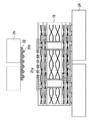
図1は、本発明の実施の形態1に係る半導体装置の配線基板を示す断面図であり、図2はその上面図であり、図3はその下面図である。 1 is a cross-sectional view showing a wiring board of a semiconductor device according to Embodiment 1 of the present invention, FIG. 2 is a top view thereof, and FIG. 3 is a bottom view thereof.
この配線基板10は、コア基板11の上面にビルドアップ基板12a,12bを重ね、下面にビルドアップ基板12c,12dを重ねて、真空プレス等を用いて熱圧着させて一体化させたものである。ただし、配線基板10の反りを防ぐために、コア基板11の上下には同じ枚数のビルドアップ基板を張り合わせている。
The
そして、コア基板11及びビルドアップ基板12a〜12dは、それぞれガラスクロスに絶縁性樹脂を含浸させて板状に固形化した層を含む。ここで、ガラスクロスは、長いガラス繊維からなる織布でも、短いガラス繊維からなる不織布でもよい。そして、ガラスクロスの代わりに、絶縁性樹脂に比べて剛性が高い他の絶縁材料、例えばカーボンファイバー等からなるクロスを用いることもできる。
And the core board |
また、絶縁性樹脂としては、例えばポリサルホン、ポリエーテルサルホン、ポリフェニルサルホン、ポリフタルアミド、ポリアミドイミド、ポリケトン、ポリアセタール、ポリイミド、ポリカーボネート、変性ポリフェニレンエーテル、ポリブチレンテレフタレート、ポリアリレート、ポリスルホン、ポリフェニレンスルフィド、ポリエーテルエーテルケトン、テトラフルオロエチレン、エポキシ、及びビスマレイミド系樹脂等を用いることができる。 Examples of the insulating resin include polysulfone, polyethersulfone, polyphenylsulfone, polyphthalamide, polyamideimide, polyketone, polyacetal, polyimide, polycarbonate, modified polyphenylene ether, polybutylene terephthalate, polyarylate, polysulfone, and polyphenylene. Sulfide, polyether ether ketone, tetrafluoroethylene, epoxy, bismaleimide resin, and the like can be used.
また、コア基板11には、ドリルによりスルーホール13が形成されている。スルーホール13の径は100〜300μmであり、ここでは200μmである。そして、スルーホール13の側壁にはCu等からなるスルーホールビア14がメッキ法等により形成されている。また、コア基板11の上面に、Cu等からなる配線層15がめっき法及びフォトリソグラフィ等により形成されている。そして、コア基板11の下面に、Cu等からなる配線層16が同様にして形成されている。この配線層15と配線層16は、スルーホールビア14を介して接続されている。
Further, a
また、ビルドアップ基板12a〜12dにも、それぞれスルーホール17が形成されている。ただし、ビルドアップ基板12a〜12dはコア基板11に比べて薄く、微細な加工が容易であるため、ビルドアップ基板12a〜12dのスルーホール17はコア基板11のスルーホール13に比べて径が小さく、具体的には30〜100μmであり、ここでは50μmとする。このスルーホール17の形成にはUV−YGAレーザ、炭酸ガスレーザ、エキシマレーザ、プラズマを用いるドライエッチング法等を用いることができる。
The through-
また、ビルドアップ基板12a〜12d上には、それぞれCu等からなる配線層18がめっき法及びフォトリソグラフィ等により形成されている。そして、スルーホール17にCu等の導電ペーストを充填することで、スルーホールビア19が形成されている。
In addition,
また、配線基板10の表面はソルダーレジスト20で覆われている。このソルダーレジスト20には開口が設けられ、最上位及び最下位の配線層18の一部が露出している。ソルダーレジスト20としては、エポキシ系、ポリイミド系、アクリル系、BT系等の電気的及び熱的に優れている樹脂を用いることができる。
Further, the surface of the
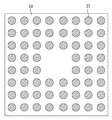
そして、露出している最上位の配線層18上に、鉛フリー半田からなるバンプ21aがメッキ法や蒸着法により形成されている。このバンプ21aは配線基板10上に格子状に並べられている。図2においては、バンプ21aは、半導体チップ22が配置される領域にフルマトリックス状に配置されているが、様々な配列が適宜選択可能である。また、鉛フリー半田とは、鉛が含まれていないか、又は環境負荷が少ない程度(1wt%未満)の鉛しか含まれていない半田である。ここでは、鉛フリー半田として、SnにCuが1〜3%含有したものを用いる。
A
図4は、半導体チップの側面図であり、図5はその下面図である。半導体チップ22の実装面に、鉛フリー半田からなるバンプ21bがメッキ法や蒸着法により形成されている。半導体チップ22の部分拡大断面図を図23に記載する。半導体チップ22は、シリコン基板100と、シリコン基板100上に形成されたMOSFETなどの半導体素子101と、SiO2絶縁膜102、SiCNエッチングストッパ膜103、SiOC低誘電率膜104及びSiOF密着膜105の積層構造からなる層間絶縁膜と、この層間絶縁膜に埋め込まれたタングステンプラグやCu配線などからなるチップ内配線層106と、層間絶縁膜上に形成されたアルミパッド層107と、アルミパッド107を露出するように開口が形成されたSiO2/SiN積層膜からなる無機パシベーション膜108及びポリイミド膜(PiQ膜)からなる有機パシベーション膜109の積層膜と、アルミパッド107上に形成された例えばTi/Cu/Ni積層膜からなるバリアメタル110と、バリアメタル110上に形成された半田バンプ21bとを備えている。半導体チップ22内の層間絶縁膜として、SiO2膜の誘電率K=4.3よりも低い誘電率の膜を使用する場合、層間絶縁膜の強度低下が問題となる。特に、一般的なSiO2膜であるTEOS膜などに比較して、膜の密度を低下させることで誘電率を低減するポーラスLow−k膜においてはその問題は顕著であり、チップにかかる応力を低減する技術は、半導体装置の信頼性を向上する上で非常に重要となる。本実施の形態においては、低誘電率膜としてポーラスSiOC膜を採用する。このポーラスSiOC膜は、主にSi−CH3基を多く含むメチル含有ポリシロキサンであり、CH3の存在により分子構造内に間隙を生じるために多孔質となり、誘電率が低下している。また、半導体チップ22を構成する材料としては、上記に具体例を示したが、これらに限る物ではなく、例えば、低誘電率膜として、SiOCHベースのポーラス低誘電率膜や、Nano Clustering Silica膜などのポーラスシリカ系材料、ポーラスHSQと呼ばれるH含有ポリシロキサン、有機ポリマー膜、有機ポリマーのポーラス膜などが適宜使用可能である。
4 is a side view of the semiconductor chip, and FIG. 5 is a bottom view thereof.
次に、上記の配線基板10上に半導体チップ22をフリップチップボンドする工程について説明する。
Next, a process of flip chip bonding the
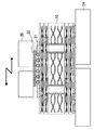
まず、図6に示すように、ボンディングステージ24上の所定の位置に、配線基板10を載置する。そして、ボンディングヘッド25の下面に、バンプ21bを形成した面を下にして半導体チップ22を真空吸着する。そして、ボンディングヘッド25を水平移動させて、半導体チップ22を配線基板10の上方に位置させる。
First, as shown in FIG. 6, the
この際、ボンディングステージ24は、内蔵しているヒータ(不図示)により配線基板10を150℃程度に加熱する。同様に、ボンディングヘッド25は、内蔵しているヒータ(不図示)により半導体チップ22を150℃程度に加熱する。
At this time, the
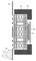
次に、図7に示すように、ボンディングヘッド25を下降させ、半導体チップ22のバンプ21bと配線基板10のバンプ21aとを圧接させる。この状態で、ボンディングヘッド25により半導体チップ22を半田融点以上の260℃程度に加熱し、バンプ21a,21bを溶融した状態で、ボンディングヘッド25を水平方向又は垂直方向へ周期的に律動(スクラブ)させる。この結果、バンプ21aとバンプ21bが一体化してバンプ21が形成される。
Next, as shown in FIG. 7, the
その後、ボンディングヘッド25を半田融点より低い温度に冷却し、バンプ21を固化する。そして、ボンディングヘッド25による半導体チップ22の吸着を解除し、ボンディングヘッド25を上昇させて、ボンディングを終了させる。図8は、配線基板の上面に半導体チップをフリップチップボンドした状態を示す上面図である。
Thereafter, the
上記の工程により、フラックスを用いることなく配線基板10に半導体チップ22をバンプ21を介してフリップチップボンドを行うことができるため、フラックスの洗浄工程を省略することができる。また、フラックス残渣の膨張によりバンプ21内にボイドが形成されることがないため、信頼性を向上させることができる。
Through the above steps, the
次に、熱応力等によりバンプ21が損傷するのを防止するために、半導体チップ22と配線基板10との間にアンダーフィル樹脂を設ける工程について説明する。
Next, a process of providing an underfill resin between the
まず、図9に示すように、配線基板10及び半導体チップ22をO2プラズマに晒す。このO2プラズマはアルゴンスパッタ等に比べて狭い隙間にも入り込むため、半導体チップ22と配線基板10の間隙にもO2プラズマを供給することができる。
First, as shown in FIG. 9, the
このプラズマ処理によって、配線基板10や半導体チップ22の表面保護膜(例えばポリイミド膜などの有機樹脂膜)が清浄化され、また活性化(粗面化)される。これにより、後で形成するアンダーフィル樹脂との密着性を向上することができる。また、半導体チップ22と配線基板10の間隙におけるアンダーフィル樹脂の充填率を向上することができる。
By this plasma treatment, the surface protective film (for example, an organic resin film such as a polyimide film) of the
次に、図10に示すように、半導体チップ22と配線基板10の間隙に、ペースト状または液状のアンダーフィル樹脂28を注入する。アンダーフィル樹脂28としては、エポキシ樹脂等の熱硬化性樹脂を用いることができ、フィラーなどを含有させてもよい。
Next, as shown in FIG. 10, a paste-like or
ここで、アンダーフィル樹脂として、ガラス転移温度(Tg)が100〜120℃、例えば110℃のものを用いる。ただし、Tgの測定方法には様々なものがあるが、ここではDMA法(引張り法)を用いる。 Here, as the underfill resin, one having a glass transition temperature (Tg) of 100 to 120 ° C., for example, 110 ° C. is used. However, there are various methods for measuring Tg, but here, the DMA method (tensile method) is used.
次に、図11に示すように、配線基板10及び半導体チップ22をベーク炉29内に入れ、従来よりも低温である125℃程度で6時間程度のべークを行う。これにより、アンダーフィル樹脂28を硬化する。
Next, as shown in FIG. 11, the
このようにTgを100℃以上とすることで、一般的に動作信頼性が求められる125℃〜150℃程度でも、アンダーフィル樹脂の弾性率を確保することができる。このため、バンプを十分に保護することができる。 Thus, by setting Tg to 100 ° C. or higher, the elastic modulus of the underfill resin can be secured even at about 125 ° C. to 150 ° C., which generally requires operation reliability. For this reason, the bump can be sufficiently protected.
また、Tgを120℃以下とすることで樹脂硬化温度(キュア温度)を低くすることができる。このため、アンダーフィル樹脂を硬化した後、樹脂硬化温度から低温へ変化させた場合の温度差を小さくすることができ、チップにかかる内部応力を小さくすることができる。 Moreover, resin hardening temperature (cure temperature) can be made low by Tg being 120 degrees C or less. For this reason, after hardening underfill resin, the temperature difference at the time of changing from resin hardening temperature to low temperature can be made small, and the internal stress concerning a chip | tip can be made small.
次に、半導体チップ22の裏面(実装面と反対側の面)にヒートスプレッダーを接着する工程について説明する。
Next, a process of adhering a heat spreader to the back surface (surface opposite to the mounting surface) of the
まず、図12に示すように、半導体チップ22の裏面に放熱樹脂31を塗布する。次に、図13に示すように、半導体チップ22の裏面にヒートスプレッダー32を放熱樹脂31により接着する。なお、ヒートスプレッダー32の材質としては、放熱性を考慮して、Cu,Al,Al−Si−Cu合金などを用いることができる。
First, as shown in FIG. 12, a
スティフナーをコスト削減のため省略し、ヒートスプレッダーのチップ周囲に突出する部分と、配線基板上面との間に、チップの厚さと同等以上の隙間を有する形状とするため、放熱樹脂31が薄いと半導体チップ22にクラックやダメージが入り易くなる。一方、放熱樹脂31が厚いと熱の発散特性が悪くなる。従って、放熱樹脂31の厚み(ギャップ)を高精度に制御する必要がある。
The stiffener is omitted for cost reduction, and the
そこで、放熱樹脂31に混入するフィラーのサイズを最適化して、放熱樹脂31の厚みを制御する。ここでは、フィラーの平均粒径が13μmのものを用いる。ただし、フィラーのサイズには分布があるので、メッシュを用いて、粒径が45μm以上のものをカットする。これにより、放熱樹脂の厚みを60±20μmに制御することができる。
Therefore, the thickness of the
即ち、放熱樹脂の所望の厚みをAとし、フィラーの最大粒径をBMAXとして、
A×4/5≧BMAX
の関係を有するようにフィラーを選択する。これにより、放熱樹脂の厚みを所望の厚みを中心とした一定の範囲内に制御することができる。放熱樹脂31としては、作業性の容易さや、熱伝導率の高さから、シリコーン系の熱硬化型放熱樹脂を用いるのが好ましい。シリコーン系放熱樹脂は、シリコーンオイルを基剤に、アルミナなど熱伝導性の高い粉末を配合した樹脂である。硬化前の状態では、粘性の高いグリース状の製品であるため、治具の位置制御を利用することによって、放熱樹脂31の厚さを比較的容易に、かつ、かなり高い精度で制御することができる。放熱樹脂31の粘性としては、少なくともアンダーフィル樹脂28の注入時の粘性よりも高い物が好ましい。フィラーの最大粒径BMAXとしては、放熱樹脂の厚みAの4/5以下に限らないが、放熱樹脂の厚みが最も小さくなる部分AMINよりも、フィラーの最大粒径BMAXが小さくなる関係であることが好ましい。BMAXが、AMINと同じ、又はそれよりも大きくなると、ヒートスプレッダー32と半導体チップ22裏面との間に、フィラーが挟み込まれる可能性が高くなる。特に、本実施の形態のように、半導体チップ22の周囲に、スティフナーなど、ヒートスプレッダー32を強固に支える構造を有さない場合は、ヒートスプレッダーを貼り付ける工程において、荷重制御のみによって放熱樹脂の厚みを制御しようとすると、ヒートスプレッダー32と半導体チップ22との間に挟まれたフィラーによって、半導体チップ22裏面にクラックが入り、半導体装置の信頼性を落とす可能性がある。
That is, the desired thickness of the heat radiation resin is A, and the maximum particle size of the filler is B MAX .
A × 4/5 ≧ B MAX
The filler is selected so as to have the following relationship. Thereby, the thickness of the heat radiating resin can be controlled within a certain range centered on a desired thickness. As the
また、フィラーの形状を球形にして、半導体チップ22やヒートスプレッダー32に対するダメージを小さくする。ここで、フィラーの形状が厳密に球形でない場合は、フィラーの粒径は、最も長い所の径とする。
In addition, the filler is made spherical to reduce damage to the
次に、図14に示すように、配線基板10、半導体チップ22及びヒートスプレッダー32をべーク炉29内に入れてべークを行い、放熱樹脂31を硬化する。これにより、半導体チップ22上にヒートスプレッダー32を搭載する。
Next, as shown in FIG. 14, the
図15は、半導体チップ22上にヒートスプレッダー32を搭載した状態を示す上面図である。ヒートスプレッダー32は配線基板10に比べて小さくする。これにより、コストを低減することができる。ただし、放熱性を確保するために、ヒートスプレッダー32は半導体チップ22より大きくする。
FIG. 15 is a top view showing a state in which the
次に、配線基板10の下面に、外部接続端子となる半田ボールを接合する工程について説明する。
Next, a process for bonding a solder ball serving as an external connection terminal to the lower surface of the
まず、図16に示すように、配線基板10の上面を下にして、配線基板10の上面(半導体チップ22を搭載した面)であってヒートスプレッダー32よりも外側の部分と配線基板10の側面とに接する保持手段33により配線基板10を保持する。これにより、半導体チップ22及びヒートスプレッダー32へストレスを与えることなく配線基板10を保持することができる
First, as shown in FIG. 16, with the upper surface of the
そして、配線基板10を保持した状態で、配線基板10の下面にマスク34を介してフラックス35を塗布する。これにより、配線基板10の下面で露出している配線層18にフラックス35が塗布される。ただし、フラックス35の代わりに半田ペーストを塗布してもよい。
Then, the
次に、図17に示すように、ボール搭載ヘッド36の下面に、鉛フリー半田からなる半田ボール37を真空吸着する。そして、ボール搭載ヘッド36を水平移動させて、半田ボール37を配線基板10の上方に位置させる。そして、ボール搭載ヘッド36を下降させて、半田ボール37を配線基板10のフラックス35上に搭載する。その後、ボール搭載ヘッド36による半田ボール37の吸着を解除し、ボール搭載ヘッド36を上昇させる。
Next, as shown in FIG. 17, a
次に、図18に示すように、半田ボール37を上に向けて配線基板10を保持手段33により保持した状態でコンベア38に載せ、リフロー炉39内に入れ、リフローを行って、半田ボール37を配線基板10に接合する。その後、洗浄を行ってフラックス35を除去する。図19は、半田ボールを接合した配線基板の下面図である。
Next, as shown in FIG. 18, the
次に、図20に示すように、配線基板10の半田ボール37を接合した面を下に向けて、バネ等の弾性部材からなるテストピン41上に半田ボール37を位置合わせする。そして、上側から押え治具42により配線基板10を押えることで、配線基板10の半田ボール37をテストピン41に押し付ける。ただし、押え治具42はヒートスプレッダー32及び半導体チップ22を内包する空間を有し、配線基板10の上面であってヒートスプレッダー32よりも外側の部分を押える。
Next, as shown in FIG. 20, the
この状態で、テストピン41と半田ボール37との間で電気信号をやり取りすることで、配線基板10及び半導体チップ22の電気的テストを行う。
In this state, an electrical signal is exchanged between the
以上の工程により、図21に示すような本発明の実施の形態1に係る半導体装置が完成する。その後、上記の半導体装置は、半田ボール37を用いてマザーボード等に実装される。
Through the above steps, the semiconductor device according to the first embodiment of the present invention as shown in FIG. 21 is completed. Thereafter, the semiconductor device is mounted on a mother board or the like using
この半導体装置は、従来は配線基板を補強し前記ヒートスプレッダーの平坦性を持たせるために設けられていたスティフナーをコスト削減のために省略し、ヒートスプレッダーのチップ周囲に突出する部分の大部分と、配線基板上面との間に、チップの厚さと同等以上の隙間を有する形状としている。アンダーフィル樹脂28の量が多い場合には、ヒートスプレッダーのチップ周囲に突出する部分のごく一部と、配線基板上面との間を埋めるような形状になる場合があるが、スティフナーを有する場合に比較して、配線基板の補強の効果はごく限定的である。このように、チップ周囲の配線基板上面の大部分が露出する形状においては、配線基板自体の剛性の向上が重要となる。そして、配線基板10において、コア基板11だけでなく、ビルドアップ基板12a〜12dもガラスクロスを含有する。
In this semiconductor device, the stiffener conventionally provided to reinforce the wiring board and have the flatness of the heat spreader is omitted for cost reduction, and most of the portion protruding around the chip of the heat spreader The gap is equal to or greater than the thickness of the chip between the upper surface of the wiring board. When the amount of the
即ち、配線基板10は、それぞれ径が異なるスルーホールが設けられた複数の絶縁基板(コア基板11とビルドアップ基板12a〜12d)を有し、各絶縁基板がガラスクロスを含有する。また、配線基板10は、径が100μm以下のスルーホールが設けられた絶縁基板(ビルドアップ基板12a〜12d)を有し、この絶縁基板もガラスクロスを含有する。
That is, the
これにより、配線基板10全体として剛性を高くすることができる。従って、コスト削減のためにスティフナーを省略した場合でも、配線基板10の反りや歪みを防ぐことができる。また、ビルドアップ基板12a〜12dを構成する絶縁層には、コア基板11に比較して、より微細なスルーホールの形成が要求される。スルーホールの直径を小さくすることにより、配線を配置できる部分の面積が広くなり、配線レイアウトの自由度が向上する。特に、半導体チップ22に形成される電極の数、すなわちバンプ21の数が、例えば数百個以上と多い場合には、バンプ21と接続する最上層の配線層18のレイアウト自由度の確保が重要となる。そこで、最上層の配線層18と接続するスルーホールビア19がその内部に形成されるビルドアップ基板12bには、微細加工における加工精度の確保が不可欠となる。本実施の形態においては、ビルドアップ基板12a〜12dの加工精度を確保するため、ビルドアップ基板12a〜12dが含有するガラスクロスの厚さを、コア基板11が含有するガラスクロスの厚さよりも薄くしている。また、ビルドアップ基板12a〜12dの厚さも、コア基板11よりも薄くしている。このように、コア基板11に比較して、薄いガラスクロスを使用し、かつビルドアップ基板12a〜12d各層も薄くする事により、ビルドアップ基板12a〜12dの剛性を保ちつつ、加工精度を向上し、微細なスルーホール17の形成を容易にしている。また、本実施の形態に記載のように、半導体チップ22として、従来のSiO2層間絶縁膜の替わりに、例えばTEOS膜に比較して脆弱なポーラス低誘電率膜などを有するものを用いる場合、ガラスクロスによって強度を増したピルドアップ基板12a〜12dを採用することは特に有効である。即ち、ビルドアップ基板12a〜12dの強度を増すことによって、半導体チップ22に及ぼす内部応力を軽減でき、半導体チップ22内部の脆弱層での剥離の発生を防ぐことができる。また、半導体チップ22として、その主面上には、ポリイミドパシベーション膜などの有機系パシベーション膜が形成されていることが好ましい。ポリイミドなど有機系パシベーション膜は、SiN膜など無機系パシベーション膜に比較して、アンダーフィル樹脂28との密着性が高い。有機系パシベーション膜で半導体チップ22の主面上を覆うことにより、アンダーフィル樹脂28と、半導体チップ22との界面での剥離を防ぐことができる。アンダーフィル樹脂28と半導体チップ22との界面のほぼ均等な接着状態を維持することにより、局所的な応力集中による低誘電率膜内部での剥離などの問題の発生を未然に防ぐことができる。本実施の形態において、配線基板10として、各層にガラスクロスを含有することで高い剛性を有するものを用いる場合について記載した。しかし、配線基板の各層の剛性を向上させる手段としては、ガラス繊維を布状に織ったガラスクロスを用いる方法に限らず、ガラス繊維で形成した不織布型のガラスクロスを用いる方法や、短いガラス繊維を強化剤として含有させる方法などが適宜選択可能である。また、繊維の材質としても、シリカを基材とするガラスに限らず、カーボンファイバーを使用した物などを適宜選択可能である。
Thereby, rigidity can be made high as the
実施の形態2.
図22は、本発明の実施の形態2に係る半導体装置を示す断面図である。実施の形態1との相違は、配線基板10として、コア基板を用いず、径が100μm以下のスルーホールが設けられた薄い絶縁基板43a〜43dを真空プレス等により熱圧着させて一体化させたものを用いる。ただし、各絶縁基板43a〜43dは、それぞれガラスクロスに絶縁性樹脂を含浸させて板状に固形化した層を含む。その他の構成は実施の形態1と同様である。
Embodiment 2. FIG.
FIG. 22 is a sectional view showing a semiconductor device according to the second embodiment of the present invention. The difference from the first embodiment is that the core substrate is not used as the
これにより、配線基板10全体として剛性を高くすることができる。従って、コスト削減のためにスティフナーを省略した場合でも、配線基板10の反りや歪みを防ぐことができる。
Thereby, rigidity can be made high as the
実施の形態3.
実施の形態3では、放熱樹脂31に混入するフィラーとして実施の形態1よりも小さいものを用いて、放熱性を向上させる。具体的には、平均粒径が5.8μm、最大粒径が24μmのフィラーを用いる。
Embodiment 3 FIG.
In the third embodiment, the heat dissipation is improved by using a filler that is smaller than that in the first embodiment as the filler mixed in the
そして、放熱樹脂31の厚みを制御するために、放熱樹脂31に球形ジルコニアからなるスペーサを混入する。具体的には、平均粒径25μm、最大粒径33μmのスペーサを用いる。このスペーサにより、放熱樹脂31の厚みを60±20μmに制御することができる。
In order to control the thickness of the
即ち、放熱樹脂の所望の厚みをAとし、スペーサの平均粒径をCとして、
A×9/10≧C
の関係を有するようにスペーサを選択する。これにより、放熱樹脂の厚みを所望の厚みを中心とした一定の範囲内に制御することができる。
That is, the desired thickness of the heat dissipation resin is A, and the average particle size of the spacer is C.
A × 9/10 ≧ C
The spacer is selected so as to have the following relationship. Thereby, the thickness of the heat radiating resin can be controlled within a certain range centered on a desired thickness.
そして、フィラーの最大粒径をBMAX、スペーサの最大粒径をCMAXとして、
CMAX>BMAX
の関係を有するようにスペーサを選択する。これにより、フィラーではなくスペーサにより放熱樹脂の厚みを制御することができる。
The maximum particle size of the filler is B MAX and the maximum particle size of the spacer is C MAX .
C MAX > B MAX
The spacer is selected so as to have the following relationship. Thereby, the thickness of the heat radiation resin can be controlled not by the filler but by the spacer.
また、フィラーの平均粒径をBとし、スペーサの最小粒径をCMINとし、フィラーの専有率90%を占める粒径をB90%として、
C>BMAX
CMIN>B
CMIN>B90%
の何れかの関係を有するようにスペーサを選択する。これにより、スペーサの利用効率を向上することができる。
Further, the average particle size of the filler is B, the minimum particle size of the spacer is C MIN, and the particle size occupying 90% of the filler is 90% ,
C> B MAX
C MIN > B
C MIN > B 90%
The spacer is selected so as to have any one of the following relationships. Thereby, the utilization efficiency of a spacer can be improved.
また、放熱性を向上させるために、スペーサの放熱樹脂における含有率は10volume%以下、好ましくは5volume%以下にする。 Further, in order to improve heat dissipation, the content of the spacer in the heat dissipation resin is set to 10 volume% or less, preferably 5 volume% or less.
実施の形態4.
実施の形態4では、半導体チップ22とヒートスプレッダー32を接着する放熱樹脂31のフロー性を以下の値に設定する。ここで、放熱樹脂31のフロー性を、室温25℃中において10mm上方から1gの放熱樹脂を平面上に滴下させ、その放熱樹脂の広がりを測定することで決めるものとする。
Embodiment 4 FIG.
In the fourth embodiment, the flow property of the
従来は、この測定方法において広がりが19mmのフロー性の放熱樹脂を用いていた。しかし、スティフナーを省略した場合、半導体チップ22上にヒートスプレッダー32を搭載した後の搬送において、マウントしてからキュアするまではまだ樹脂は固まってない液体状態なので、振動・傾斜によってヒートスプレッダー32のずれが発生するという問題があった。
Conventionally, a flowable heat radiating resin having a spread of 19 mm was used in this measurement method. However, when the stiffener is omitted, since the resin is not in a liquid state until it is cured after mounting after the
これに対し、実施の形態4では、上記の測定方法において広がりが4mm以上12mm以下、例えば8mmのフロー性の放熱樹脂を用いる。このように、広がりが12mm以下のフロー性の放熱樹脂を用いることにより、ヒートスプレッダー32のずれを防ぐことができる。また、広がりが4mm以上のフロー性の放熱樹脂を用いることにより、半導体チップ22上に放熱樹脂31を塗布した場合に十分に濡れ広がるため、ボイドの発生を防ぐことができる。
On the other hand, in the fourth embodiment, in the above measurement method, a heat radiating resin having a spread of 4 mm to 12 mm, for example, 8 mm is used. Thus, the use of the flowable heat radiating resin having a spread of 12 mm or less can prevent the
10 配線基板
11 コア基板
12a〜12d ビルドアップ基板
13,17 スルーホール
14,19 スルーホールビア
15,16,18 配線層
21a,21b,21 バンプ
22 半導体チップ
28 アンダーフィル樹脂
31 放熱樹脂
32 ヒートスプレッダー
33 保持手段
37 半田ボール
41 テストピン
42 押え治具
43a〜43d 絶縁基板
DESCRIPTION OF
Claims (5)
複数の半導体素子が形成された主面と前記主面の反対側の裏面とを有し、前記配線基板の前記第1ビルドアップ基板上に複数の第1バンプ電極を介してフリップチップ接続された半導体チップと、
前記配線基板の前記第1ビルドアップ基板と前記半導体チップの間に、前記複数の第1バンプ電極を囲むように形成された樹脂層と、
前記配線基板の前記第2ビルドアップ基板上に配置された複数の第2バンプ電極とを備え、
前記コア基板は、第1絶縁層と、前記第1絶緑層を厚さ方向に貫通する複数の第1スルーホールと、前記第1絶緑層の上面及び下面に形成され、前記第1スルーホールを介して接続された第1配線層とを有し、
前記第1及び第2ビルドアップ基板の各々は、第2絶縁層と、前記第2絶縁層を厚さ方向に貫通する複数の第2スルーホールと、前記第2絶縁層の上面及び下面に形成され、前記第2スルーホールを介して接続された第2配線層とを有し、
前記第1及び第2ビルドアップ基板の前記複数の第2スルーホールの直径は、前記コア基板の前記第1スルーホールの直径より小さく形成され、
前記コア基板の前記第1絶縁層と、前記第1及び第2ビルドアップ基板の前記第2絶縁層は、それぞれガラスクロスを含有し、
前記半導体チップは、シリコン基板と、前記シリコン基板上に形成された多層配線構造と、前記多層配線構造を覆うように形成されたパッシベーション膜と、前記パッシベーション膜から露出するように形成された複数のパッド電極とを有し、
前記複数の第1バンプ電極は、前記半導体チップの前記複数のパッド電極にそれぞれ接続され、
前記パッシベーション膜は、SiO 2 膜を含み、
前記多層配線構造は、前記パッシベーション膜の前記SiO 2 膜より低誘電率を持つ層間絶縁膜を有することを特徴とする半導体装置。 A wiring substrate having a core substrate, a first buildup substrate formed on an upper surface of the core substrate, and a second buildup substrate formed on a lower surface of the core substrate;
The semiconductor device has a main surface on which a plurality of semiconductor elements are formed and a back surface opposite to the main surface, and is flip-chip connected to the first buildup substrate of the wiring substrate via a plurality of first bump electrodes. A semiconductor chip;
A resin layer formed between the first build-up substrate of the wiring substrate and the semiconductor chip so as to surround the plurality of first bump electrodes;
A plurality of second bump electrodes disposed on the second buildup substrate of the wiring board;
The core substrate is formed on a first insulating layer, a plurality of first through holes penetrating the first green layer in a thickness direction, and an upper surface and a lower surface of the first green layer, and the first through layer A first wiring layer connected through a hole,
Each of the first and second build-up substrates is formed on a second insulating layer, a plurality of second through holes penetrating the second insulating layer in a thickness direction, and an upper surface and a lower surface of the second insulating layer. And a second wiring layer connected through the second through hole,
The diameters of the plurality of second through holes of the first and second buildup boards are formed smaller than the diameter of the first through holes of the core board,
The first insulating layer of the core substrate and the second insulating layer of the first and second buildup substrates each contain glass cloth ,
The semiconductor chip includes a silicon substrate, a multilayer wiring structure formed on the silicon substrate, a passivation film formed so as to cover the multilayer wiring structure, and a plurality of layers formed so as to be exposed from the passivation film. A pad electrode,
The plurality of first bump electrodes are respectively connected to the plurality of pad electrodes of the semiconductor chip,
The passivation film includes a SiO 2 film,
The semiconductor device according to claim 1, wherein the multilayer wiring structure includes an interlayer insulating film having a dielectric constant lower than that of the SiO 2 film of the passivation film .
ことを特徴とする請求項1に記載の半導体装置。The semiconductor device according to claim 1.
Priority Applications (16)
| Application Number | Priority Date | Filing Date | Title |
|---|---|---|---|
| JP2006096999A JP4534062B2 (en) | 2005-04-19 | 2006-03-31 | Semiconductor device |
| US11/406,337 US7521799B2 (en) | 2005-04-19 | 2006-04-19 | Semiconductor device and method of manufacturing the same |
| US12/401,193 US7791204B2 (en) | 2005-04-19 | 2009-03-10 | Semiconductor device and method of manufacturing the same |
| US12/753,521 US8018066B2 (en) | 2005-04-19 | 2010-04-02 | Semiconductor device and method of manufacturing the same |
| US13/183,196 US20110269273A1 (en) | 2005-04-19 | 2011-07-14 | Semiconductor device and method of manufacturing the same |
| US13/367,029 US8314495B2 (en) | 2005-04-19 | 2012-02-06 | Semiconductor device and method of manufacturing the same |
| US13/648,876 US8575757B2 (en) | 2005-04-19 | 2012-10-10 | Semiconductor device and method of manufacturing the same |
| US13/863,241 US8581410B2 (en) | 2005-04-19 | 2013-04-15 | Semiconductor device and method of manufacturing the same |
| US14/044,497 US8822269B2 (en) | 2005-04-19 | 2013-10-02 | Semiconductor device and method of manufacturing the same |
| US14/338,175 US8928147B2 (en) | 2005-04-19 | 2014-07-22 | Semiconductor device and method of manufacturing the same |
| US14/569,423 US9299681B2 (en) | 2005-04-19 | 2014-12-12 | Semiconductor device and method of manufacturing |
| US15/045,978 US9496153B2 (en) | 2005-04-19 | 2016-02-17 | Semiconductor device and method of manufacturing the same |
| US15/241,777 US9576890B2 (en) | 2005-04-19 | 2016-08-19 | Semiconductor device and method of manufacturing the same |
| US15/398,444 US9831166B2 (en) | 2005-04-19 | 2017-01-04 | Semiconductor device |
| US15/796,746 US10283444B2 (en) | 2005-04-19 | 2017-10-27 | Semiconductor device and method of manufacturing the same |
| US16/359,485 US10714415B2 (en) | 2005-04-19 | 2019-03-20 | Semiconductor device and method of manufacturing the same |
Applications Claiming Priority (2)
| Application Number | Priority Date | Filing Date | Title |
|---|---|---|---|
| JP2005121063 | 2005-04-19 | ||
| JP2006096999A JP4534062B2 (en) | 2005-04-19 | 2006-03-31 | Semiconductor device |
Related Child Applications (1)
| Application Number | Title | Priority Date | Filing Date |
|---|---|---|---|
| JP2009168196A Division JP5293477B2 (en) | 2005-04-19 | 2009-07-16 | Semiconductor device |
Publications (3)
| Publication Number | Publication Date |
|---|---|
| JP2006324642A JP2006324642A (en) | 2006-11-30 |
| JP2006324642A5 JP2006324642A5 (en) | 2009-09-03 |
| JP4534062B2 true JP4534062B2 (en) | 2010-09-01 |
Family
ID=37233663
Family Applications (1)
| Application Number | Title | Priority Date | Filing Date |
|---|---|---|---|
| JP2006096999A Active JP4534062B2 (en) | 2005-04-19 | 2006-03-31 | Semiconductor device |
Country Status (2)
| Country | Link |
|---|---|
| US (15) | US7521799B2 (en) |
| JP (1) | JP4534062B2 (en) |
Cited By (2)
| Publication number | Priority date | Publication date | Assignee | Title |
|---|---|---|---|---|
| US8890001B2 (en) | 2012-01-27 | 2014-11-18 | Kyocera Slc Technologies Corporation | Wiring board and mounting structure using the same |
| US8957321B2 (en) | 2011-09-26 | 2015-02-17 | Kyocera Slc Technologies Corporation | Printed circuit board, mount structure thereof, and methods of producing these |
Families Citing this family (65)
| Publication number | Priority date | Publication date | Assignee | Title |
|---|---|---|---|---|
| JP4534062B2 (en) | 2005-04-19 | 2010-09-01 | ルネサスエレクトロニクス株式会社 | Semiconductor device |
| CN102790018A (en) * | 2006-12-05 | 2012-11-21 | 住友电木株式会社 | Semiconductor package, core layer material, buildup layer material, and sealing resin composition |
| TWI416673B (en) * | 2007-03-30 | 2013-11-21 | Sumitomo Bakelite Co | Connection structure for flip-chip semiconductor package, build-up layer material, sealing resin composition, and circuit substrate |
| JP5018182B2 (en) * | 2007-03-30 | 2012-09-05 | ルネサスエレクトロニクス株式会社 | Manufacturing method of semiconductor device |
| WO2009022461A1 (en) * | 2007-08-10 | 2009-02-19 | Sanyo Electric Co., Ltd. | Circuit device, circuit device manufacturing method and portable device |
| US20100043694A1 (en) * | 2008-08-20 | 2010-02-25 | Patel Gordhanbhai N | Tamper evident indicating devices |
| US20100044093A1 (en) * | 2008-08-25 | 2010-02-25 | Wilinx Corporation | Layout geometries for differential signals |
| KR101627574B1 (en) * | 2008-09-22 | 2016-06-21 | 쿄세라 코포레이션 | Wiring substrate and the method of manufacturing the same |
| US8895359B2 (en) * | 2008-12-16 | 2014-11-25 | Panasonic Corporation | Semiconductor device, flip-chip mounting method and flip-chip mounting apparatus |
| JPWO2010086952A1 (en) * | 2009-01-30 | 2012-07-26 | パナソニック株式会社 | Semiconductor device and manufacturing method thereof |
| US9420707B2 (en) * | 2009-12-17 | 2016-08-16 | Intel Corporation | Substrate for integrated circuit devices including multi-layer glass core and methods of making the same |
| US8207453B2 (en) | 2009-12-17 | 2012-06-26 | Intel Corporation | Glass core substrate for integrated circuit devices and methods of making the same |
| US8381965B2 (en) | 2010-07-22 | 2013-02-26 | Taiwan Semiconductor Manufacturing Company, Ltd. | Thermal compress bonding |
| US8946904B2 (en) * | 2010-08-27 | 2015-02-03 | Avago Technologies General Ip (Singapore) Pte. Ltd. | Substrate vias for heat removal from semiconductor die |
| US8104666B1 (en) | 2010-09-01 | 2012-01-31 | Taiwan Semiconductor Manufacturing Company, Ltd. | Thermal compressive bonding with separate die-attach and reflow processes |
| JP5581933B2 (en) * | 2010-09-22 | 2014-09-03 | ソニー株式会社 | Package substrate, module using the same, and electric / electronic device |
| US8177862B2 (en) * | 2010-10-08 | 2012-05-15 | Taiwan Semiconductor Manufacturing Co., Ltd | Thermal compressive bond head |
| US20120090883A1 (en) * | 2010-10-13 | 2012-04-19 | Qualcomm Incorporated | Method and Apparatus for Improving Substrate Warpage |
| CN102034720B (en) | 2010-11-05 | 2013-05-15 | 南通富士通微电子股份有限公司 | Chip packaging method |
| CN102034721B (en) * | 2010-11-05 | 2013-07-10 | 南通富士通微电子股份有限公司 | Method for encapsulating chip |
| US8643154B2 (en) * | 2011-01-31 | 2014-02-04 | Ibiden Co., Ltd. | Semiconductor mounting device having multiple substrates connected via bumps |
| JP5853389B2 (en) * | 2011-03-28 | 2016-02-09 | ソニー株式会社 | Semiconductor device and manufacturing method of semiconductor device. |
| JP2012256675A (en) * | 2011-06-08 | 2012-12-27 | Shinko Electric Ind Co Ltd | Wiring board, semiconductor device, and manufacturing method of semiconductor device |
| TWI473551B (en) | 2011-07-08 | 2015-02-11 | Unimicron Technology Corp | Package substrate and fabrication method thereof |
| US20130026660A1 (en) * | 2011-07-29 | 2013-01-31 | Namics Corporation | Liquid epoxy resin composition for semiconductor encapsulation, and semiconductor device using the same |
| JP5820673B2 (en) | 2011-09-15 | 2015-11-24 | 新光電気工業株式会社 | Semiconductor device and manufacturing method thereof |
| US8633588B2 (en) * | 2011-12-21 | 2014-01-21 | Mediatek Inc. | Semiconductor package |
| US9257276B2 (en) | 2011-12-31 | 2016-02-09 | Intel Corporation | Organic thin film passivation of metal interconnections |
| WO2013101243A1 (en) | 2011-12-31 | 2013-07-04 | Intel Corporation | High density package interconnects |
| US8497579B1 (en) * | 2012-02-16 | 2013-07-30 | Chipbond Technology Corporation | Semiconductor packaging method and structure thereof |
| WO2013133827A1 (en) | 2012-03-07 | 2013-09-12 | Intel Corporation | Glass clad microelectronic substrate |
| KR101382811B1 (en) * | 2012-03-14 | 2014-04-08 | 엘지이노텍 주식회사 | The printed circuit board and the method for manufacturing the same |
| US9001520B2 (en) | 2012-09-24 | 2015-04-07 | Intel Corporation | Microelectronic structures having laminated or embedded glass routing structures for high density packaging |
| US9615453B2 (en) | 2012-09-26 | 2017-04-04 | Ping-Jung Yang | Method for fabricating glass substrate package |
| US10622310B2 (en) | 2012-09-26 | 2020-04-14 | Ping-Jung Yang | Method for fabricating glass substrate package |
| JP2015038911A (en) * | 2012-09-27 | 2015-02-26 | イビデン株式会社 | Printed wiring board and method of manufacturing printed wiring board |
| EP2743972A1 (en) * | 2012-12-17 | 2014-06-18 | Imec | Method for bonding semiconductor substrates and devices obtained thereby |
| JP5941847B2 (en) * | 2013-01-17 | 2016-06-29 | 信越化学工業株式会社 | Silicone / organic resin composite laminate, method for producing the same, and light-emitting semiconductor device using the same |
| JP2014168007A (en) * | 2013-02-28 | 2014-09-11 | Kyocer Slc Technologies Corp | Wiring board and manufacturing method of the same |
| US9704829B2 (en) | 2013-03-06 | 2017-07-11 | Win Semiconductor Corp. | Stacked structure of semiconductor chips having via holes and metal bumps |
| TWI524487B (en) * | 2013-03-06 | 2016-03-01 | 穩懋半導體股份有限公司 | A fabrication method of a semiconductor chip with substrate via holes and metal bumps |
| CN105247972A (en) * | 2013-04-26 | 2016-01-13 | 株式会社电装 | Multi-layer substrate, electronic device using multi-layer substrate, manufacturing method for multi-layer substrate, substrate, and electronic device using substrate |
| US20150101846A1 (en) * | 2013-10-14 | 2015-04-16 | Samsung Electro-Mechanics Co., Ltd. | Printed circuit board and method of manufacturing the same |
| KR101548816B1 (en) * | 2013-11-11 | 2015-08-31 | 삼성전기주식회사 | Printed circuit board and method of manufacturing the same |
| US9799626B2 (en) * | 2014-09-15 | 2017-10-24 | Invensas Corporation | Semiconductor packages and other circuit modules with porous and non-porous stabilizing layers |
| KR102411998B1 (en) * | 2015-06-25 | 2022-06-22 | 삼성전기주식회사 | Circuit board and method of manufacturing the same |
| KR102458034B1 (en) | 2015-10-16 | 2022-10-25 | 삼성전자주식회사 | Semiconductor package, Method of fabricating the Semiconductor package, And Semiconductor module |
| JP2017108070A (en) * | 2015-12-11 | 2017-06-15 | 新光電気工業株式会社 | Wiring board, semiconductor device and wiring board manufacturing method |
| US9812446B2 (en) * | 2016-03-30 | 2017-11-07 | Toyota Motor Engineering & Manufacturing North America, Inc. | Electronic apparatus with pocket of low permittivity material to reduce electromagnetic interference |
| JP6751910B2 (en) | 2016-10-05 | 2020-09-09 | パナソニックIpマネジメント株式会社 | Manufacturing method of multi-layer printed wiring board and multi-layer printed wiring board |
| US11276667B2 (en) * | 2016-12-31 | 2022-03-15 | Intel Corporation | Heat removal between top and bottom die interface |
| US11201066B2 (en) | 2017-01-31 | 2021-12-14 | Skyworks Solutions, Inc. | Control of under-fill using a dam on a packaging substrate for a dual-sided ball grid array package |
| DE102017205247A1 (en) * | 2017-03-28 | 2018-10-04 | Robert Bosch Gmbh | electronic module |
| WO2018213265A1 (en) * | 2017-05-15 | 2018-11-22 | Apex Industrial Technologies Llc | Motorized door assembly with safety features for heated cabinet |
| KR20190018812A (en) | 2017-08-16 | 2019-02-26 | 삼성전기주식회사 | Semiconductor package and electronic device having the same |
| DE112018006764T5 (en) * | 2018-01-05 | 2020-09-10 | Sony Semiconductor Solutions Corporation | SEMI-CONDUCTOR DEVICE |
| CN108649023B (en) * | 2018-03-28 | 2020-03-03 | 宁波市鄞州路麦电子有限公司 | Lead frame and preparation method thereof |
| JP7139862B2 (en) * | 2018-10-15 | 2022-09-21 | 株式会社デンソー | semiconductor equipment |
| JP7225787B2 (en) * | 2018-12-25 | 2023-02-21 | Tdk株式会社 | Circuit board with built-in semiconductor IC and its manufacturing method |
| JP7163205B2 (en) * | 2019-01-18 | 2022-10-31 | ルネサスエレクトロニクス株式会社 | semiconductor equipment |
| KR20210082969A (en) * | 2019-12-26 | 2021-07-06 | 삼성전자주식회사 | Semiconductor package |
| US20220069489A1 (en) * | 2020-08-28 | 2022-03-03 | Unimicron Technology Corp. | Circuit board structure and manufacturing method thereof |
| US11545425B2 (en) * | 2020-10-08 | 2023-01-03 | Qualcomm Incorporated | Substrate comprising interconnects embedded in a solder resist layer |
| US11823983B2 (en) | 2021-03-23 | 2023-11-21 | Qualcomm Incorporated | Package with a substrate comprising pad-on-pad interconnects |
| CN113709972A (en) * | 2021-09-27 | 2021-11-26 | 合肥移瑞通信技术有限公司 | Circuit board, manufacturing method thereof and packaging piece |
Citations (4)
| Publication number | Priority date | Publication date | Assignee | Title |
|---|---|---|---|---|
| JP2001217514A (en) * | 2000-02-03 | 2001-08-10 | Denso Corp | Multi-layered wiring board |
| JP2004083905A (en) * | 2002-08-07 | 2004-03-18 | Dow Corning Toray Silicone Co Ltd | Thermally conductive filler, thermally conductive silicone elastomer composition and semiconductor device |
| JP2004134679A (en) * | 2002-10-11 | 2004-04-30 | Dainippon Printing Co Ltd | Core substrate, manufacturing method thereof, and multilayer wiring board |
| JP2004296843A (en) * | 2003-03-27 | 2004-10-21 | Fujitsu Ltd | Semiconductor device |
Family Cites Families (80)
| Publication number | Priority date | Publication date | Assignee | Title |
|---|---|---|---|---|
| US5917707A (en) | 1993-11-16 | 1999-06-29 | Formfactor, Inc. | Flexible contact structure with an electrically conductive shell |
| JPH02278821A (en) | 1989-04-20 | 1990-11-15 | Fuji Electric Co Ltd | Patterning of polycrystalline silicon |
| JPH02278831A (en) | 1989-04-20 | 1990-11-15 | Fujitsu Ltd | Formation of solder bump |
| JP2830504B2 (en) | 1991-05-16 | 1998-12-02 | 松下電工株式会社 | Substrate for mounting semiconductor devices |
| JPH05251596A (en) | 1992-03-06 | 1993-09-28 | Sony Corp | Ic chip package structure of flip chip system |
| US5677045A (en) | 1993-09-14 | 1997-10-14 | Hitachi, Ltd. | Laminate and multilayer printed circuit board |
| JPH07221125A (en) | 1994-01-27 | 1995-08-18 | Toyota Autom Loom Works Ltd | Mounting structure of semiconductor device and insulating adhesive agent |
| JP4295943B2 (en) | 1994-09-01 | 2009-07-15 | 株式会社東芝 | Semiconductor device |
| US6004887A (en) | 1994-09-01 | 1999-12-21 | Kabushiki Kaisha Toshiba | Semiconductor device with improved adhesion between titanium-based metal wiring layer and insulation film |
| US5753975A (en) | 1994-09-01 | 1998-05-19 | Kabushiki Kaisha Toshiba | Semiconductor device with improved adhesion between titanium-based metal wiring layer and insulation film |
| JPH08162455A (en) | 1994-12-06 | 1996-06-21 | Toshiba Corp | Spherical electrode forming method and device |
| JP3274314B2 (en) | 1995-06-08 | 2002-04-15 | 東芝マイクロエレクトロニクス株式会社 | Resin-sealed semiconductor device and method of manufacturing the same |
| JPH0982882A (en) | 1995-09-20 | 1997-03-28 | Nec Corp | Multi-chip module |
| US6008071A (en) | 1995-09-20 | 1999-12-28 | Fujitsu Limited | Method of forming solder bumps onto an integrated circuit device |
| US5956605A (en) | 1996-09-20 | 1999-09-21 | Micron Technology, Inc. | Use of nitrides for flip-chip encapsulation |
| JP3629345B2 (en) | 1996-12-12 | 2005-03-16 | 新光電気工業株式会社 | Flip chip mounting method |
| AU8502798A (en) | 1997-07-21 | 1999-02-10 | Aguila Technologies, Inc. | Semiconductor flip-chip package and method for the fabrication thereof |
| JP2000022040A (en) | 1998-07-07 | 2000-01-21 | Mitsubishi Electric Corp | Semiconductor device and manufacture thereof |
| JP3152209B2 (en) | 1998-07-07 | 2001-04-03 | 日本電気株式会社 | Semiconductor device and manufacturing method thereof |
| JP3116926B2 (en) | 1998-11-16 | 2000-12-11 | 日本電気株式会社 | Package structure and semiconductor device, package manufacturing method, and semiconductor device manufacturing method |
| JP2000260817A (en) | 1999-03-11 | 2000-09-22 | Mitsubishi Electric Corp | Semiconductor device and manufacture thereof |
| JP2000307225A (en) | 1999-04-21 | 2000-11-02 | Ibiden Co Ltd | Mask for solder printing and print wiring board and manufacture thereof |
| US6184142B1 (en) | 1999-04-26 | 2001-02-06 | United Microelectronics Corp. | Process for low k organic dielectric film etch |
| JP4275806B2 (en) | 1999-06-01 | 2009-06-10 | 株式会社ルネサステクノロジ | Mounting method of semiconductor element |
| US6373717B1 (en) | 1999-07-02 | 2002-04-16 | International Business Machines Corporation | Electronic package with high density interconnect layer |
| KR20080111567A (en) * | 1999-09-02 | 2008-12-23 | 이비덴 가부시키가이샤 | Printed circuit board and method of manufacturing printed circuit board |
| JP3334693B2 (en) | 1999-10-08 | 2002-10-15 | 日本電気株式会社 | Method for manufacturing semiconductor device |
| JP3367554B2 (en) | 1999-10-13 | 2003-01-14 | 日本電気株式会社 | Flip chip package |
| JP2001127095A (en) | 1999-10-29 | 2001-05-11 | Shinko Electric Ind Co Ltd | Semiconductor device and its manufacturing method |
| TW512653B (en) | 1999-11-26 | 2002-12-01 | Ibiden Co Ltd | Multilayer circuit board and semiconductor device |
| JP3397313B2 (en) * | 1999-12-20 | 2003-04-14 | 富士通株式会社 | Semiconductor device manufacturing method and electronic component mounting method |
| US6710446B2 (en) | 1999-12-30 | 2004-03-23 | Renesas Technology Corporation | Semiconductor device comprising stress relaxation layers and method for manufacturing the same |
| JP2001230341A (en) | 2000-02-18 | 2001-08-24 | Hitachi Ltd | Semiconductor device |
| JP3677429B2 (en) * | 2000-03-09 | 2005-08-03 | Necエレクトロニクス株式会社 | Method of manufacturing flip chip type semiconductor device |
| JP2001274556A (en) | 2000-03-23 | 2001-10-05 | Nec Corp | Printed wiring board |
| JP2003535175A (en) * | 2000-05-26 | 2003-11-25 | ダウ グローバル テクノロジーズ インコーポレイテッド | Polyethylene rich / polypropylene blends and their uses |
| US6706975B2 (en) * | 2000-07-13 | 2004-03-16 | Ngk Spark Plug Co., Ltd. | Paste for filling throughhole and printed wiring board using same |
| JP4447143B2 (en) | 2000-10-11 | 2010-04-07 | 新光電気工業株式会社 | Semiconductor device and manufacturing method thereof |
| JP4421118B2 (en) | 2001-01-05 | 2010-02-24 | 富士通マイクロエレクトロニクス株式会社 | Semiconductor device manufacturing method |
| JP2002232135A (en) | 2001-01-30 | 2002-08-16 | Matsushita Electric Ind Co Ltd | Double-sided circuit board for lamination and its manufacturing method, and multilayer printed circuit board using the same |
| JP2002232102A (en) | 2001-01-31 | 2002-08-16 | Ngk Spark Plug Co Ltd | Circuit board |
| JP2002261214A (en) | 2001-03-01 | 2002-09-13 | Toshiba Corp | Semiconductor device, method of manufacturing the same and lid member |
| JP2002270717A (en) | 2001-03-12 | 2002-09-20 | Rohm Co Ltd | Semiconductor device |
| JP2002311084A (en) | 2001-04-11 | 2002-10-23 | Nec Corp | Flip-chip lsi and analysis method for flip-chip lsi |
| EP1408724A4 (en) | 2001-07-18 | 2007-05-23 | Matsushita Electric Ind Co Ltd | Circuit formed substrate and method of manufacturing circuit formed substrate |
| JP2003051568A (en) | 2001-08-08 | 2003-02-21 | Nec Corp | Semiconductor device |
| US6861757B2 (en) * | 2001-09-03 | 2005-03-01 | Nec Corporation | Interconnecting substrate for carrying semiconductor device, method of producing thereof and package of semiconductor device |
| US6617683B2 (en) | 2001-09-28 | 2003-09-09 | Intel Corporation | Thermal performance in flip chip/integral heat spreader packages using low modulus thermal interface material |
| JP2003204171A (en) | 2002-01-04 | 2003-07-18 | Karentekku:Kk | Build-up multi-layer board |
| JP2003273482A (en) | 2002-03-15 | 2003-09-26 | Fujitsu Ltd | Circuit board and manufacturing method thereof, and electronic equipment |
| US6815486B2 (en) * | 2002-04-12 | 2004-11-09 | Dow Corning Corporation | Thermally conductive phase change materials and methods for their preparation and use |
| US6794273B2 (en) * | 2002-05-24 | 2004-09-21 | Fujitsu Limited | Semiconductor device and manufacturing method thereof |
| TWI234253B (en) | 2002-05-31 | 2005-06-11 | Fujitsu Ltd | Semiconductor device and manufacturing method thereof |
| US7078822B2 (en) | 2002-06-25 | 2006-07-18 | Intel Corporation | Microelectronic device interconnects |
| US6791839B2 (en) * | 2002-06-25 | 2004-09-14 | Dow Corning Corporation | Thermal interface materials and methods for their preparation and use |
| US6936919B2 (en) | 2002-08-21 | 2005-08-30 | Texas Instruments Incorporated | Heatsink-substrate-spacer structure for an integrated-circuit package |
| JP4119205B2 (en) | 2002-08-27 | 2008-07-16 | 富士通株式会社 | Multilayer wiring board |
| JP2004095582A (en) | 2002-08-29 | 2004-03-25 | Dainippon Printing Co Ltd | Method for manufacturing core substrate |
| JP3822549B2 (en) | 2002-09-26 | 2006-09-20 | 富士通株式会社 | Wiring board |
| JP3894097B2 (en) | 2002-10-25 | 2007-03-14 | 松下電器産業株式会社 | Semiconductor device |
| AU2003269495A1 (en) | 2002-10-25 | 2004-05-13 | Matsushita Electric Industrial Co., Ltd. | Semiconductor device and resin binder for assembling semiconductor device |
| US7059512B2 (en) * | 2002-11-06 | 2006-06-13 | Ricoh Company, Ltd. | Solder alloy material layer composition, electroconductive and adhesive composition, flux material layer composition, solder ball transferring sheet, bump and bump forming process, and semiconductor device |
| JP2004158671A (en) | 2002-11-07 | 2004-06-03 | Eito Kogyo:Kk | Multilayer board and its producing process |
| US6949404B1 (en) | 2002-11-25 | 2005-09-27 | Altera Corporation | Flip chip package with warpage control |
| JP2004179545A (en) | 2002-11-28 | 2004-06-24 | Kyocera Corp | Wiring board |
| JP2004207338A (en) | 2002-12-24 | 2004-07-22 | Kyocera Corp | Wiring board |
| JP4149289B2 (en) * | 2003-03-12 | 2008-09-10 | 株式会社ルネサステクノロジ | Semiconductor device |
| JP4116911B2 (en) | 2003-03-25 | 2008-07-09 | 富士通株式会社 | Conductive ball mounting jig and conductive ball mounting method |
| JP4873827B2 (en) | 2003-04-28 | 2012-02-08 | イビデン株式会社 | Multilayer printed wiring board |
| TWI300261B (en) | 2003-07-02 | 2008-08-21 | Advanced Semiconductor Eng | Chip package structur |
| TWI229434B (en) | 2003-08-25 | 2005-03-11 | Advanced Semiconductor Eng | Flip chip stacked package |
| JP2005093556A (en) | 2003-09-12 | 2005-04-07 | Matsushita Electric Ind Co Ltd | Printed-circuit board and method of manufacturing same |
| US7067902B2 (en) | 2003-12-02 | 2006-06-27 | International Business Machines Corporation | Building metal pillars in a chip for structure support |
| US20050174738A1 (en) * | 2004-02-06 | 2005-08-11 | International Business Machines Corporation | Method and structure for heat sink attachment in semiconductor device packaging |
| US7119432B2 (en) | 2004-04-07 | 2006-10-10 | Lsi Logic Corporation | Method and apparatus for establishing improved thermal communication between a die and a heatspreader in a semiconductor package |
| CN100499056C (en) * | 2004-06-09 | 2009-06-10 | 株式会社瑞萨科技 | Process for fabricating semiconductor integrated circuit device |
| JP2006019636A (en) | 2004-07-05 | 2006-01-19 | Renesas Technology Corp | Semiconductor apparatus |
| EP1844089B1 (en) * | 2004-12-16 | 2010-09-08 | Dow Corning Corporation | Amide-substituted silicones and methods for their preparation and use |
| JP4534062B2 (en) * | 2005-04-19 | 2010-09-01 | ルネサスエレクトロニクス株式会社 | Semiconductor device |
| JP5035997B2 (en) | 2008-05-29 | 2012-09-26 | ルネサスエレクトロニクス株式会社 | A / D converter |
-
2006
- 2006-03-31 JP JP2006096999A patent/JP4534062B2/en active Active
- 2006-04-19 US US11/406,337 patent/US7521799B2/en active Active
-
2009
- 2009-03-10 US US12/401,193 patent/US7791204B2/en active Active
-
2010
- 2010-04-02 US US12/753,521 patent/US8018066B2/en active Active
-
2011
- 2011-07-14 US US13/183,196 patent/US20110269273A1/en not_active Abandoned
-
2012
- 2012-02-06 US US13/367,029 patent/US8314495B2/en active Active
- 2012-10-10 US US13/648,876 patent/US8575757B2/en active Active
-
2013
- 2013-04-15 US US13/863,241 patent/US8581410B2/en active Active
- 2013-10-02 US US14/044,497 patent/US8822269B2/en active Active
-
2014
- 2014-07-22 US US14/338,175 patent/US8928147B2/en active Active
- 2014-12-12 US US14/569,423 patent/US9299681B2/en active Active
-
2016
- 2016-02-17 US US15/045,978 patent/US9496153B2/en active Active
- 2016-08-19 US US15/241,777 patent/US9576890B2/en active Active
-
2017
- 2017-01-04 US US15/398,444 patent/US9831166B2/en active Active
- 2017-10-27 US US15/796,746 patent/US10283444B2/en active Active
-
2019
- 2019-03-20 US US16/359,485 patent/US10714415B2/en active Active
Patent Citations (4)
| Publication number | Priority date | Publication date | Assignee | Title |
|---|---|---|---|---|
| JP2001217514A (en) * | 2000-02-03 | 2001-08-10 | Denso Corp | Multi-layered wiring board |
| JP2004083905A (en) * | 2002-08-07 | 2004-03-18 | Dow Corning Toray Silicone Co Ltd | Thermally conductive filler, thermally conductive silicone elastomer composition and semiconductor device |
| JP2004134679A (en) * | 2002-10-11 | 2004-04-30 | Dainippon Printing Co Ltd | Core substrate, manufacturing method thereof, and multilayer wiring board |
| JP2004296843A (en) * | 2003-03-27 | 2004-10-21 | Fujitsu Ltd | Semiconductor device |
Cited By (2)
| Publication number | Priority date | Publication date | Assignee | Title |
|---|---|---|---|---|
| US8957321B2 (en) | 2011-09-26 | 2015-02-17 | Kyocera Slc Technologies Corporation | Printed circuit board, mount structure thereof, and methods of producing these |
| US8890001B2 (en) | 2012-01-27 | 2014-11-18 | Kyocera Slc Technologies Corporation | Wiring board and mounting structure using the same |
Also Published As
| Publication number | Publication date |
|---|---|
| US20110269273A1 (en) | 2011-11-03 |
| US20160358846A1 (en) | 2016-12-08 |
| US7791204B2 (en) | 2010-09-07 |
| US20190221509A1 (en) | 2019-07-18 |
| US8822269B2 (en) | 2014-09-02 |
| US20150099331A1 (en) | 2015-04-09 |
| US9576890B2 (en) | 2017-02-21 |
| US20140038361A1 (en) | 2014-02-06 |
| JP2006324642A (en) | 2006-11-30 |
| US20130228913A1 (en) | 2013-09-05 |
| US20140327137A1 (en) | 2014-11-06 |
| US7521799B2 (en) | 2009-04-21 |
| US8581410B2 (en) | 2013-11-12 |
| US9831166B2 (en) | 2017-11-28 |
| US10714415B2 (en) | 2020-07-14 |
| US20090174065A1 (en) | 2009-07-09 |
| US8575757B2 (en) | 2013-11-05 |
| US20170117216A1 (en) | 2017-04-27 |
| US20160196987A1 (en) | 2016-07-07 |
| US9299681B2 (en) | 2016-03-29 |
| US8928147B2 (en) | 2015-01-06 |
| US20100187679A1 (en) | 2010-07-29 |
| US8018066B2 (en) | 2011-09-13 |
| US10283444B2 (en) | 2019-05-07 |
| US8314495B2 (en) | 2012-11-20 |
| US20130037947A1 (en) | 2013-02-14 |
| US20180068936A1 (en) | 2018-03-08 |
| US20120133045A1 (en) | 2012-05-31 |
| US20060244128A1 (en) | 2006-11-02 |
| US9496153B2 (en) | 2016-11-15 |
Similar Documents
| Publication | Publication Date | Title |
|---|---|---|
| JP4534062B2 (en) | Semiconductor device | |
| JP4108643B2 (en) | Wiring board and semiconductor package using the same | |
| JP2004335641A (en) | Method of manufacturing substrate having built-in semiconductor element | |
| JP2003007916A (en) | Method of manufacturing circuit device | |
| JP2003007922A (en) | Method of manufacturing circuit device | |
| JP6123836B2 (en) | Manufacturing method of semiconductor device | |
| JP4599121B2 (en) | Electrical relay plate | |
| JP5309472B2 (en) | Manufacturing method of semiconductor device | |
| JP2001185642A (en) | Package substrate for mounting semiconductor | |
| JP2003133656A (en) | Mounting structure of semiconductor element | |
| JP2004134821A (en) | Semiconductor apparatus | |
| TW202209516A (en) | Method for manufacturing electronic component |
Legal Events
| Date | Code | Title | Description |
|---|---|---|---|
| A621 | Written request for application examination |
Free format text: JAPANESE INTERMEDIATE CODE: A621 Effective date: 20090212 |
|
| A521 | Request for written amendment filed |
Free format text: JAPANESE INTERMEDIATE CODE: A523 Effective date: 20090716 |
|
| A871 | Explanation of circumstances concerning accelerated examination |
Free format text: JAPANESE INTERMEDIATE CODE: A871 Effective date: 20090716 |
|
| A977 | Report on retrieval |
Free format text: JAPANESE INTERMEDIATE CODE: A971007 Effective date: 20091001 |
|
| A975 | Report on accelerated examination |
Free format text: JAPANESE INTERMEDIATE CODE: A971005 Effective date: 20091023 |
|
| A131 | Notification of reasons for refusal |
Free format text: JAPANESE INTERMEDIATE CODE: A131 Effective date: 20091104 |
|
| A521 | Request for written amendment filed |
Free format text: JAPANESE INTERMEDIATE CODE: A523 Effective date: 20091224 |
|
| A131 | Notification of reasons for refusal |
Free format text: JAPANESE INTERMEDIATE CODE: A131 Effective date: 20100406 |
|
| A521 | Request for written amendment filed |
Free format text: JAPANESE INTERMEDIATE CODE: A523 Effective date: 20100412 |
|
| TRDD | Decision of grant or rejection written | ||
| A01 | Written decision to grant a patent or to grant a registration (utility model) |
Free format text: JAPANESE INTERMEDIATE CODE: A01 Effective date: 20100518 |
|
| A01 | Written decision to grant a patent or to grant a registration (utility model) |
Free format text: JAPANESE INTERMEDIATE CODE: A01 |
|
| A711 | Notification of change in applicant |
Free format text: JAPANESE INTERMEDIATE CODE: A712 Effective date: 20100521 |
|
| A61 | First payment of annual fees (during grant procedure) |
Free format text: JAPANESE INTERMEDIATE CODE: A61 Effective date: 20100524 |
|
| FPAY | Renewal fee payment (event date is renewal date of database) |
Free format text: PAYMENT UNTIL: 20130625 Year of fee payment: 3 |
|
| R150 | Certificate of patent or registration of utility model |
Ref document number: 4534062 Country of ref document: JP Free format text: JAPANESE INTERMEDIATE CODE: R150 Free format text: JAPANESE INTERMEDIATE CODE: R150 |
|
| FPAY | Renewal fee payment (event date is renewal date of database) |
Free format text: PAYMENT UNTIL: 20130625 Year of fee payment: 3 |
|
| FPAY | Renewal fee payment (event date is renewal date of database) |
Free format text: PAYMENT UNTIL: 20140625 Year of fee payment: 4 |
|
| S531 | Written request for registration of change of domicile |
Free format text: JAPANESE INTERMEDIATE CODE: R313531 |
|
| R350 | Written notification of registration of transfer |
Free format text: JAPANESE INTERMEDIATE CODE: R350 |