JP4488684B2 - Multilayer printed wiring board - Google Patents
Multilayer printed wiring board Download PDFInfo
- Publication number
- JP4488684B2 JP4488684B2 JP2003064986A JP2003064986A JP4488684B2 JP 4488684 B2 JP4488684 B2 JP 4488684B2 JP 2003064986 A JP2003064986 A JP 2003064986A JP 2003064986 A JP2003064986 A JP 2003064986A JP 4488684 B2 JP4488684 B2 JP 4488684B2
- Authority
- JP
- Japan
- Prior art keywords
- layer
- conductor layer
- conductor
- core substrate
- thickness
- Prior art date
- Legal status (The legal status is an assumption and is not a legal conclusion. Google has not performed a legal analysis and makes no representation as to the accuracy of the status listed.)
- Expired - Lifetime
Links
Images


Classifications
-
- H—ELECTRICITY
- H05—ELECTRIC TECHNIQUES NOT OTHERWISE PROVIDED FOR
- H05K—PRINTED CIRCUITS; CASINGS OR CONSTRUCTIONAL DETAILS OF ELECTRIC APPARATUS; MANUFACTURE OF ASSEMBLAGES OF ELECTRICAL COMPONENTS
- H05K1/00—Printed circuits
- H05K1/02—Details
- H05K1/09—Use of materials for the conductive, e.g. metallic pattern
-
- H—ELECTRICITY
- H05—ELECTRIC TECHNIQUES NOT OTHERWISE PROVIDED FOR
- H05K—PRINTED CIRCUITS; CASINGS OR CONSTRUCTIONAL DETAILS OF ELECTRIC APPARATUS; MANUFACTURE OF ASSEMBLAGES OF ELECTRICAL COMPONENTS
- H05K3/00—Apparatus or processes for manufacturing printed circuits
- H05K3/46—Manufacturing multilayer circuits
-
- H—ELECTRICITY
- H01—ELECTRIC ELEMENTS
- H01L—SEMICONDUCTOR DEVICES NOT COVERED BY CLASS H10
- H01L23/00—Details of semiconductor or other solid state devices
- H01L23/48—Arrangements for conducting electric current to or from the solid state body in operation, e.g. leads, terminal arrangements ; Selection of materials therefor
- H01L23/488—Arrangements for conducting electric current to or from the solid state body in operation, e.g. leads, terminal arrangements ; Selection of materials therefor consisting of soldered or bonded constructions
- H01L23/498—Leads, i.e. metallisations or lead-frames on insulating substrates, e.g. chip carriers
- H01L23/49811—Additional leads joined to the metallisation on the insulating substrate, e.g. pins, bumps, wires, flat leads
- H01L23/49816—Spherical bumps on the substrate for external connection, e.g. ball grid arrays [BGA]
-
- H—ELECTRICITY
- H01—ELECTRIC ELEMENTS
- H01L—SEMICONDUCTOR DEVICES NOT COVERED BY CLASS H10
- H01L23/00—Details of semiconductor or other solid state devices
- H01L23/48—Arrangements for conducting electric current to or from the solid state body in operation, e.g. leads, terminal arrangements ; Selection of materials therefor
- H01L23/488—Arrangements for conducting electric current to or from the solid state body in operation, e.g. leads, terminal arrangements ; Selection of materials therefor consisting of soldered or bonded constructions
- H01L23/498—Leads, i.e. metallisations or lead-frames on insulating substrates, e.g. chip carriers
- H01L23/49822—Multilayer substrates
-
- H—ELECTRICITY
- H05—ELECTRIC TECHNIQUES NOT OTHERWISE PROVIDED FOR
- H05K—PRINTED CIRCUITS; CASINGS OR CONSTRUCTIONAL DETAILS OF ELECTRIC APPARATUS; MANUFACTURE OF ASSEMBLAGES OF ELECTRICAL COMPONENTS
- H05K1/00—Printed circuits
- H05K1/02—Details
-
- H—ELECTRICITY
- H05—ELECTRIC TECHNIQUES NOT OTHERWISE PROVIDED FOR
- H05K—PRINTED CIRCUITS; CASINGS OR CONSTRUCTIONAL DETAILS OF ELECTRIC APPARATUS; MANUFACTURE OF ASSEMBLAGES OF ELECTRICAL COMPONENTS
- H05K1/00—Printed circuits
- H05K1/18—Printed circuits structurally associated with non-printed electric components
- H05K1/182—Printed circuits structurally associated with non-printed electric components associated with components mounted in the printed circuit board, e.g. insert mounted components [IMC]
- H05K1/183—Components mounted in and supported by recessed areas of the printed circuit board
-
- H—ELECTRICITY
- H05—ELECTRIC TECHNIQUES NOT OTHERWISE PROVIDED FOR
- H05K—PRINTED CIRCUITS; CASINGS OR CONSTRUCTIONAL DETAILS OF ELECTRIC APPARATUS; MANUFACTURE OF ASSEMBLAGES OF ELECTRICAL COMPONENTS
- H05K3/00—Apparatus or processes for manufacturing printed circuits
- H05K3/46—Manufacturing multilayer circuits
- H05K3/4602—Manufacturing multilayer circuits characterized by a special circuit board as base or central core whereon additional circuit layers are built or additional circuit boards are laminated
- H05K3/4608—Manufacturing multilayer circuits characterized by a special circuit board as base or central core whereon additional circuit layers are built or additional circuit boards are laminated comprising an electrically conductive base or core
-
- H—ELECTRICITY
- H01—ELECTRIC ELEMENTS
- H01L—SEMICONDUCTOR DEVICES NOT COVERED BY CLASS H10
- H01L2224/00—Indexing scheme for arrangements for connecting or disconnecting semiconductor or solid-state bodies and methods related thereto as covered by H01L24/00
- H01L2224/01—Means for bonding being attached to, or being formed on, the surface to be connected, e.g. chip-to-package, die-attach, "first-level" interconnects; Manufacturing methods related thereto
- H01L2224/02—Bonding areas; Manufacturing methods related thereto
- H01L2224/04—Structure, shape, material or disposition of the bonding areas prior to the connecting process
- H01L2224/05—Structure, shape, material or disposition of the bonding areas prior to the connecting process of an individual bonding area
- H01L2224/0554—External layer
- H01L2224/0556—Disposition
- H01L2224/05568—Disposition the whole external layer protruding from the surface
-
- H—ELECTRICITY
- H01—ELECTRIC ELEMENTS
- H01L—SEMICONDUCTOR DEVICES NOT COVERED BY CLASS H10
- H01L2224/00—Indexing scheme for arrangements for connecting or disconnecting semiconductor or solid-state bodies and methods related thereto as covered by H01L24/00
- H01L2224/01—Means for bonding being attached to, or being formed on, the surface to be connected, e.g. chip-to-package, die-attach, "first-level" interconnects; Manufacturing methods related thereto
- H01L2224/02—Bonding areas; Manufacturing methods related thereto
- H01L2224/04—Structure, shape, material or disposition of the bonding areas prior to the connecting process
- H01L2224/05—Structure, shape, material or disposition of the bonding areas prior to the connecting process of an individual bonding area
- H01L2224/0554—External layer
- H01L2224/05573—Single external layer
-
- H—ELECTRICITY
- H01—ELECTRIC ELEMENTS
- H01L—SEMICONDUCTOR DEVICES NOT COVERED BY CLASS H10
- H01L2224/00—Indexing scheme for arrangements for connecting or disconnecting semiconductor or solid-state bodies and methods related thereto as covered by H01L24/00
- H01L2224/01—Means for bonding being attached to, or being formed on, the surface to be connected, e.g. chip-to-package, die-attach, "first-level" interconnects; Manufacturing methods related thereto
- H01L2224/10—Bump connectors; Manufacturing methods related thereto
- H01L2224/15—Structure, shape, material or disposition of the bump connectors after the connecting process
- H01L2224/16—Structure, shape, material or disposition of the bump connectors after the connecting process of an individual bump connector
- H01L2224/161—Disposition
- H01L2224/16151—Disposition the bump connector connecting between a semiconductor or solid-state body and an item not being a semiconductor or solid-state body, e.g. chip-to-substrate, chip-to-passive
- H01L2224/16221—Disposition the bump connector connecting between a semiconductor or solid-state body and an item not being a semiconductor or solid-state body, e.g. chip-to-substrate, chip-to-passive the body and the item being stacked
- H01L2224/16225—Disposition the bump connector connecting between a semiconductor or solid-state body and an item not being a semiconductor or solid-state body, e.g. chip-to-substrate, chip-to-passive the body and the item being stacked the item being non-metallic, e.g. insulating substrate with or without metallisation
-
- H—ELECTRICITY
- H01—ELECTRIC ELEMENTS
- H01L—SEMICONDUCTOR DEVICES NOT COVERED BY CLASS H10
- H01L2924/00—Indexing scheme for arrangements or methods for connecting or disconnecting semiconductor or solid-state bodies as covered by H01L24/00
- H01L2924/0001—Technical content checked by a classifier
- H01L2924/00014—Technical content checked by a classifier the subject-matter covered by the group, the symbol of which is combined with the symbol of this group, being disclosed without further technical details
-
- H—ELECTRICITY
- H01—ELECTRIC ELEMENTS
- H01L—SEMICONDUCTOR DEVICES NOT COVERED BY CLASS H10
- H01L2924/00—Indexing scheme for arrangements or methods for connecting or disconnecting semiconductor or solid-state bodies as covered by H01L24/00
- H01L2924/01—Chemical elements
- H01L2924/01019—Potassium [K]
-
- H—ELECTRICITY
- H01—ELECTRIC ELEMENTS
- H01L—SEMICONDUCTOR DEVICES NOT COVERED BY CLASS H10
- H01L2924/00—Indexing scheme for arrangements or methods for connecting or disconnecting semiconductor or solid-state bodies as covered by H01L24/00
- H01L2924/01—Chemical elements
- H01L2924/01025—Manganese [Mn]
-
- H—ELECTRICITY
- H01—ELECTRIC ELEMENTS
- H01L—SEMICONDUCTOR DEVICES NOT COVERED BY CLASS H10
- H01L2924/00—Indexing scheme for arrangements or methods for connecting or disconnecting semiconductor or solid-state bodies as covered by H01L24/00
- H01L2924/01—Chemical elements
- H01L2924/01046—Palladium [Pd]
-
- H—ELECTRICITY
- H01—ELECTRIC ELEMENTS
- H01L—SEMICONDUCTOR DEVICES NOT COVERED BY CLASS H10
- H01L2924/00—Indexing scheme for arrangements or methods for connecting or disconnecting semiconductor or solid-state bodies as covered by H01L24/00
- H01L2924/01—Chemical elements
- H01L2924/01078—Platinum [Pt]
-
- H—ELECTRICITY
- H01—ELECTRIC ELEMENTS
- H01L—SEMICONDUCTOR DEVICES NOT COVERED BY CLASS H10
- H01L2924/00—Indexing scheme for arrangements or methods for connecting or disconnecting semiconductor or solid-state bodies as covered by H01L24/00
- H01L2924/01—Chemical elements
- H01L2924/01079—Gold [Au]
-
- H—ELECTRICITY
- H01—ELECTRIC ELEMENTS
- H01L—SEMICONDUCTOR DEVICES NOT COVERED BY CLASS H10
- H01L2924/00—Indexing scheme for arrangements or methods for connecting or disconnecting semiconductor or solid-state bodies as covered by H01L24/00
- H01L2924/095—Indexing scheme for arrangements or methods for connecting or disconnecting semiconductor or solid-state bodies as covered by H01L24/00 with a principal constituent of the material being a combination of two or more materials provided in the groups H01L2924/013 - H01L2924/0715
- H01L2924/097—Glass-ceramics, e.g. devitrified glass
- H01L2924/09701—Low temperature co-fired ceramic [LTCC]
-
- H—ELECTRICITY
- H01—ELECTRIC ELEMENTS
- H01L—SEMICONDUCTOR DEVICES NOT COVERED BY CLASS H10
- H01L2924/00—Indexing scheme for arrangements or methods for connecting or disconnecting semiconductor or solid-state bodies as covered by H01L24/00
- H01L2924/15—Details of package parts other than the semiconductor or other solid state devices to be connected
- H01L2924/151—Die mounting substrate
- H01L2924/153—Connection portion
- H01L2924/1531—Connection portion the connection portion being formed only on the surface of the substrate opposite to the die mounting surface
- H01L2924/15311—Connection portion the connection portion being formed only on the surface of the substrate opposite to the die mounting surface being a ball array, e.g. BGA
-
- H—ELECTRICITY
- H01—ELECTRIC ELEMENTS
- H01L—SEMICONDUCTOR DEVICES NOT COVERED BY CLASS H10
- H01L2924/00—Indexing scheme for arrangements or methods for connecting or disconnecting semiconductor or solid-state bodies as covered by H01L24/00
- H01L2924/15—Details of package parts other than the semiconductor or other solid state devices to be connected
- H01L2924/151—Die mounting substrate
- H01L2924/153—Connection portion
- H01L2924/1531—Connection portion the connection portion being formed only on the surface of the substrate opposite to the die mounting surface
- H01L2924/15312—Connection portion the connection portion being formed only on the surface of the substrate opposite to the die mounting surface being a pin array, e.g. PGA
-
- H—ELECTRICITY
- H01—ELECTRIC ELEMENTS
- H01L—SEMICONDUCTOR DEVICES NOT COVERED BY CLASS H10
- H01L2924/00—Indexing scheme for arrangements or methods for connecting or disconnecting semiconductor or solid-state bodies as covered by H01L24/00
- H01L2924/19—Details of hybrid assemblies other than the semiconductor or other solid state devices to be connected
- H01L2924/191—Disposition
- H01L2924/19101—Disposition of discrete passive components
- H01L2924/19106—Disposition of discrete passive components in a mirrored arrangement on two different side of a common die mounting substrate
-
- H—ELECTRICITY
- H01—ELECTRIC ELEMENTS
- H01L—SEMICONDUCTOR DEVICES NOT COVERED BY CLASS H10
- H01L2924/00—Indexing scheme for arrangements or methods for connecting or disconnecting semiconductor or solid-state bodies as covered by H01L24/00
- H01L2924/30—Technical effects
- H01L2924/301—Electrical effects
- H01L2924/3011—Impedance
-
- H—ELECTRICITY
- H01—ELECTRIC ELEMENTS
- H01L—SEMICONDUCTOR DEVICES NOT COVERED BY CLASS H10
- H01L2924/00—Indexing scheme for arrangements or methods for connecting or disconnecting semiconductor or solid-state bodies as covered by H01L24/00
- H01L2924/30—Technical effects
- H01L2924/35—Mechanical effects
- H01L2924/351—Thermal stress
- H01L2924/3511—Warping
-
- H—ELECTRICITY
- H05—ELECTRIC TECHNIQUES NOT OTHERWISE PROVIDED FOR
- H05K—PRINTED CIRCUITS; CASINGS OR CONSTRUCTIONAL DETAILS OF ELECTRIC APPARATUS; MANUFACTURE OF ASSEMBLAGES OF ELECTRICAL COMPONENTS
- H05K1/00—Printed circuits
- H05K1/02—Details
- H05K1/0213—Electrical arrangements not otherwise provided for
- H05K1/0237—High frequency adaptations
-
- H—ELECTRICITY
- H05—ELECTRIC TECHNIQUES NOT OTHERWISE PROVIDED FOR
- H05K—PRINTED CIRCUITS; CASINGS OR CONSTRUCTIONAL DETAILS OF ELECTRIC APPARATUS; MANUFACTURE OF ASSEMBLAGES OF ELECTRICAL COMPONENTS
- H05K1/00—Printed circuits
- H05K1/02—Details
- H05K1/03—Use of materials for the substrate
- H05K1/05—Insulated conductive substrates, e.g. insulated metal substrate
- H05K1/056—Insulated conductive substrates, e.g. insulated metal substrate the metal substrate being covered by an organic insulating layer
-
- H—ELECTRICITY
- H05—ELECTRIC TECHNIQUES NOT OTHERWISE PROVIDED FOR
- H05K—PRINTED CIRCUITS; CASINGS OR CONSTRUCTIONAL DETAILS OF ELECTRIC APPARATUS; MANUFACTURE OF ASSEMBLAGES OF ELECTRICAL COMPONENTS
- H05K1/00—Printed circuits
- H05K1/18—Printed circuits structurally associated with non-printed electric components
- H05K1/182—Printed circuits structurally associated with non-printed electric components associated with components mounted in the printed circuit board, e.g. insert mounted components [IMC]
- H05K1/185—Components encapsulated in the insulating substrate of the printed circuit or incorporated in internal layers of a multilayer circuit
-
- H—ELECTRICITY
- H05—ELECTRIC TECHNIQUES NOT OTHERWISE PROVIDED FOR
- H05K—PRINTED CIRCUITS; CASINGS OR CONSTRUCTIONAL DETAILS OF ELECTRIC APPARATUS; MANUFACTURE OF ASSEMBLAGES OF ELECTRICAL COMPONENTS
- H05K2201/00—Indexing scheme relating to printed circuits covered by H05K1/00
- H05K2201/03—Conductive materials
- H05K2201/0332—Structure of the conductor
- H05K2201/0335—Layered conductors or foils
- H05K2201/0347—Overplating, e.g. for reinforcing conductors or bumps; Plating over filled vias
-
- H—ELECTRICITY
- H05—ELECTRIC TECHNIQUES NOT OTHERWISE PROVIDED FOR
- H05K—PRINTED CIRCUITS; CASINGS OR CONSTRUCTIONAL DETAILS OF ELECTRIC APPARATUS; MANUFACTURE OF ASSEMBLAGES OF ELECTRICAL COMPONENTS
- H05K2201/00—Indexing scheme relating to printed circuits covered by H05K1/00
- H05K2201/03—Conductive materials
- H05K2201/0332—Structure of the conductor
- H05K2201/0335—Layered conductors or foils
- H05K2201/0352—Differences between the conductors of different layers of a multilayer
-
- H—ELECTRICITY
- H05—ELECTRIC TECHNIQUES NOT OTHERWISE PROVIDED FOR
- H05K—PRINTED CIRCUITS; CASINGS OR CONSTRUCTIONAL DETAILS OF ELECTRIC APPARATUS; MANUFACTURE OF ASSEMBLAGES OF ELECTRICAL COMPONENTS
- H05K2201/00—Indexing scheme relating to printed circuits covered by H05K1/00
- H05K2201/09—Shape and layout
- H05K2201/09209—Shape and layout details of conductors
- H05K2201/0929—Conductive planes
- H05K2201/09309—Core having two or more power planes; Capacitive laminate of two power planes
-
- H—ELECTRICITY
- H05—ELECTRIC TECHNIQUES NOT OTHERWISE PROVIDED FOR
- H05K—PRINTED CIRCUITS; CASINGS OR CONSTRUCTIONAL DETAILS OF ELECTRIC APPARATUS; MANUFACTURE OF ASSEMBLAGES OF ELECTRICAL COMPONENTS
- H05K2201/00—Indexing scheme relating to printed circuits covered by H05K1/00
- H05K2201/09—Shape and layout
- H05K2201/09209—Shape and layout details of conductors
- H05K2201/095—Conductive through-holes or vias
- H05K2201/09536—Buried plated through-holes, i.e. plated through-holes formed in a core before lamination
-
- H—ELECTRICITY
- H05—ELECTRIC TECHNIQUES NOT OTHERWISE PROVIDED FOR
- H05K—PRINTED CIRCUITS; CASINGS OR CONSTRUCTIONAL DETAILS OF ELECTRIC APPARATUS; MANUFACTURE OF ASSEMBLAGES OF ELECTRICAL COMPONENTS
- H05K2201/00—Indexing scheme relating to printed circuits covered by H05K1/00
- H05K2201/09—Shape and layout
- H05K2201/09209—Shape and layout details of conductors
- H05K2201/095—Conductive through-holes or vias
- H05K2201/0959—Plated through-holes or plated blind vias filled with insulating material
-
- H—ELECTRICITY
- H05—ELECTRIC TECHNIQUES NOT OTHERWISE PROVIDED FOR
- H05K—PRINTED CIRCUITS; CASINGS OR CONSTRUCTIONAL DETAILS OF ELECTRIC APPARATUS; MANUFACTURE OF ASSEMBLAGES OF ELECTRICAL COMPONENTS
- H05K2201/00—Indexing scheme relating to printed circuits covered by H05K1/00
- H05K2201/09—Shape and layout
- H05K2201/09209—Shape and layout details of conductors
- H05K2201/095—Conductive through-holes or vias
- H05K2201/096—Vertically aligned vias, holes or stacked vias
-
- H—ELECTRICITY
- H05—ELECTRIC TECHNIQUES NOT OTHERWISE PROVIDED FOR
- H05K—PRINTED CIRCUITS; CASINGS OR CONSTRUCTIONAL DETAILS OF ELECTRIC APPARATUS; MANUFACTURE OF ASSEMBLAGES OF ELECTRICAL COMPONENTS
- H05K2201/00—Indexing scheme relating to printed circuits covered by H05K1/00
- H05K2201/09—Shape and layout
- H05K2201/09209—Shape and layout details of conductors
- H05K2201/09654—Shape and layout details of conductors covering at least two types of conductors provided for in H05K2201/09218 - H05K2201/095
- H05K2201/09809—Coaxial layout
-
- H—ELECTRICITY
- H05—ELECTRIC TECHNIQUES NOT OTHERWISE PROVIDED FOR
- H05K—PRINTED CIRCUITS; CASINGS OR CONSTRUCTIONAL DETAILS OF ELECTRIC APPARATUS; MANUFACTURE OF ASSEMBLAGES OF ELECTRICAL COMPONENTS
- H05K3/00—Apparatus or processes for manufacturing printed circuits
- H05K3/40—Forming printed elements for providing electric connections to or between printed circuits
- H05K3/42—Plated through-holes or plated via connections
- H05K3/429—Plated through-holes specially for multilayer circuits, e.g. having connections to inner circuit layers
-
- H—ELECTRICITY
- H05—ELECTRIC TECHNIQUES NOT OTHERWISE PROVIDED FOR
- H05K—PRINTED CIRCUITS; CASINGS OR CONSTRUCTIONAL DETAILS OF ELECTRIC APPARATUS; MANUFACTURE OF ASSEMBLAGES OF ELECTRICAL COMPONENTS
- H05K3/00—Apparatus or processes for manufacturing printed circuits
- H05K3/46—Manufacturing multilayer circuits
- H05K3/4602—Manufacturing multilayer circuits characterized by a special circuit board as base or central core whereon additional circuit layers are built or additional circuit boards are laminated
-
- H—ELECTRICITY
- H05—ELECTRIC TECHNIQUES NOT OTHERWISE PROVIDED FOR
- H05K—PRINTED CIRCUITS; CASINGS OR CONSTRUCTIONAL DETAILS OF ELECTRIC APPARATUS; MANUFACTURE OF ASSEMBLAGES OF ELECTRICAL COMPONENTS
- H05K3/00—Apparatus or processes for manufacturing printed circuits
- H05K3/46—Manufacturing multilayer circuits
- H05K3/4611—Manufacturing multilayer circuits by laminating two or more circuit boards
- H05K3/4641—Manufacturing multilayer circuits by laminating two or more circuit boards having integrally laminated metal sheets or special power cores
Abstract
Description
【0001】
【発明の属する技術分野】
この発明は、多層プリント配線板に係り、高周波のICチップ、特に3GHz以上の高周波領域でのICチップを実装したとしても誤作動やエラーなどが発生することなく、電気特性や信頼性を向上させることができる多層プリント配線板に関することを提案する。
【0002】
【従来の技術】
ICチップ用のパッケージを構成するビルドアップ式の多層プリント配線板では、スルーホールが形成されたコア基板の両面もしくは片面に、層間絶縁樹脂を形成し、層間導通のためのバイアホールをレーザもしくはフォトエッチングにより開口させて、層間樹脂絶縁層を形成させる。そのバイアホール上にめっきなどにより導体層を形成し、エッチングなどを経て、パターンを形成し、導体回路を作り出させる。さらに、層間絶縁層と導体層を繰り返し形成させることにより、ビルドアップ多層プリント配線板が得られる。必要に応じて、表層には半田バンプ、外部端子(PGA/BGAなど)を形成させることにより、ICチップを実装することができる基板やパッケージ基板となる。ICチップはC4(フリップチップ)実装を行うことにより、ICチップと基板との電気的接続を行っている。
【0003】
ビルドアップ式の多層プリント配線板の従来技術としては、特許文献1、特許文献2などがある。ともに、スルーホールを充填樹脂で充填されたコア基板上に、ランドが形成されて、両面にバイアホールを有する層間絶縁層を施して、アディテイブ法により導体層を施し、ランドと接続することにより、高密度化、微細配線を形成された多層プリント配線板を得られる。
【0004】
【特許文献1】
特開平6-260756号公報
【特許文献2】
特開平6-275959号公報
【0005】
【発明が解決しようとする課題】
しかしながら、ICチップが高周波になるにつれて、誤動作やエラーの発生の頻度が高くなってきた。特に周波数が3GHzを越えたあたりから、その度合いが高くなってきている。5GHzを越えると全く動かなくなることもあった。そのために、該ICチップをCPUとして備えるコンピュータで、機能すべきはずの動作、例えば、画像の認識、スイッチの切り替え、外部へのデータの伝達などの所望の機能や動作を行えなくなってしまった。
【0006】
それらのICチップ、基板をそれぞれ非破壊検査や分解したいところICチップ、基板自体には、短絡やオープンなどの問題は発生しておらず、周波数の小さい(特に1GHz未満)ICチップを実装した場合には、誤動作やエラーの発生はなかった。
【0007】
本発明は、上述した課題を解決するためになされたものであり、その目的とするところは、高周波領域のICチップ、特に3GHzを越えても誤動作やエラーの発生しないプリント基板もしくはパッケージ基板を構成し得る多層プリント配線板を提案することにある。
【0008】
【課題を解決するための手段】
発明者らは、上記目的の実現に向け鋭意研究した結果、以下に示す内容を要旨構成とする発明に想到した。すなわち、
本願発明は、コア基板上に、層間絶縁層と導体層が形成されて、バイアホールを介して、電気的な接続を行われる多層プリント配線板において、コア基板の導体層の厚みは、層間絶縁層上の導体層の厚みよりも厚いことを特徴とする多層プリント配線板にある。
【0009】
第1の効果として、コア基板の電源層の導体層が厚くすることにより、コア基板の強度が増す、それによりコア基板自体を薄くしたとしても、反りや発生した応力を基板自体で緩和することが可能となる。
【0010】
第2の効果として、導体層を厚くすることにより、導体自体の体積を増やすことができる。その体積を増やすことにより、導体での抵抗が低減することができる。そのため流れる信号線などの電気的な伝達などを阻害しなくなる。従って、伝達される信号などに損失を起こさない。それは、コアとなる部分の基板だけを厚くすることにより、その効果を奏する。
【0011】
第3の効果として、導体層を電源層として用いることで、ICチップへの電源の供給能力が向上させることができる。また、導体層をアース層として用いることで、ICチップへの信号、電源に重畳するノイズを低減させることができる。その根拠としては、第2の効果で述べた導体の抵抗の低減が、電源の供給も阻害しなくなる。そのため、該多層プリント基板上にICチップを実装したときに、ICチップ〜基板〜電源までのループインダクタンスを低減することができる。そのために、初期動作における電源不足が小さくなるため、電源不足が起き難くなり、そのためにより高周波領域のICチップを実装したとしても、初期起動における誤動作やエラーなどを引き起こすことがない。
【0012】
また、ICチップ〜基板〜コンデンサもしくは電源層〜電源を経て、ICチップに電源を供給する場合にも、同様の効果を奏する。前述のループインダクタンスを低減することができる。それ故に、コンデンサもしくは誘電体層の電源の供給に損失を起こさない。そもそもICチップは、瞬時的に電力を消費して、複雑な演算処理や動作が行われる。電源層からのICチップへの電力供給により、高周波領域のICチップを実装したとしても、初期動作における電源不足(電圧降下の発生という状況)に対して、大量のコンデンサを実装することなく、電源の供給をすることができる。そもそも高周波領域のICチップを用いるためには初期動作時の電源不足(電圧降下)が発生するが、従来のICチップでは供給されていたコンデンサもしくは誘電体層の容量で足りていた。
【0013】
特に、コア基板の電源層として用いられる導体層の厚みが、コア基板の片面もしくは両面上の層間絶縁層上に導体層の厚みより、厚いときに、上記の3つの効果を最大限にさせることができるのである。この場合の層間絶縁層上の導体層とは、絶縁層の中に心材を含浸されていない樹脂で形成された層間樹脂絶縁層に、層間を接続させるための非貫通孔であるバイアホールを形成したものにめっき、スパッタなどを経て形成された導体層を主として意味する。これ以外にも特に限定されないがバイアホールを形成されたものであれば、上記の導体層に該当する。
【0014】
コア基板の電源層は、基板の表層、内層もしくは、その両方に配置させてもよい。内層の場合は、2層以上に渡り多層化してもよい。基本的には、コア基板の電源層は層間絶縁層の導体層よりも厚くなっていれば、その効果を有するのである。
ただ、内層に形成することが望ましい。内層に形成されるとICチップと外部端もしくはコンデンサとの中間に電源層が配置される。そのため、双方の距離が均一であり、阻害原因が少なくなり、電源不足が抑えられるからである。
【0015】
また、本発明では、コア基板上に、層間絶縁層と導体層が形成されて、バイアホールを介して、電気的な接続を行われる多層プリント配線板において、
コア基板上の導体層の厚みをα1、層間絶縁層上の導体層の厚みをα2に対して、α2<α1≦40α2であることを特徴とする多層プリント配線板にある。
【0016】
α1≦α2の場合は、電源不足に対する効果が全くない。つまり、いいかえると初期動作時に発生する電圧降下に対して、その降下度を抑えるということが明確にならないということである。
α1>40α2を>越えた場合についても検討を行ったが、基本的には電気特性は、40α2とほぼ同等である。つまり、本願の効果の臨界点であると理解できる。これ以上厚くしても、電気的な効果の向上は望めない。ただ、この厚みを越えると、コア基板の表層に導体層を形成した場合にコア基板と接続を行うランド等が形成するのに困難が生じてしまう。さらに上層の層間絶縁層を形成すると、凹凸が大きくなってしまい、層間絶縁層にうねりを生じてしまうために、インピーダンスを整合することが出来なくなってしまうことがある。しかしながら、その範囲(α1>40α2)でも問題がないときもある。
【0017】
導体層の厚みα1は、1.2α2≦α1≦40α2であることがさらに望ましい。その範囲であれば、電源不足(電圧降下)によるICチップの誤動作やエラーなどが発生しないことが確認されている。
【0018】
この場合のコア基板とは、ガラスエポキシ樹脂などの芯材が含浸した樹脂基板、セラミック基板、金属基板、樹脂、セラミック、金属を複合して用いた複合コア基板、それらの基板の内層に(電源用)導体層が設けられた基板、3層以上の多層化した導体層が形成された多層コア基板を用いたもの等をさす。
【0019】
電源層の導体の厚みを、厚くするために、金属を埋め込まれた基板上に、めっき、スパッタなどの一般的に行われる導体層を形成するプリント配線板の方法で形成したものを用いてもよい。
【0020】
多層コア基板の場合であれば、コア基板の表層の導体層と内層の導体層をそれぞれ足した厚みが、コアの導体層の厚みとなる。この場合、表層の導体層と内層の導体層とが電気的な接続があり、かつ、2箇所以上での電気的な接続があるものであるときに適用される。つまり、多層化しても、コア基板の導体層の厚みを厚くすることが本質であり、効果自体はなんら変わりないのである。また、パッド、ランド程度の面積であれば、その面積の導体層の厚みは、足した厚みとはならない。導体層とは、電源層あるひはアース層であることが望ましい。
この場合は、3層(表層+内層)からなるコア基板でもよい。3層以上の多層コア基板でもよい。
必要に応じて、コア基板の内層にコンデンサや誘電体層、抵抗などの部品を埋め込み、形成させた電子部品収納コア基板を用いてもよい。
【0021】
さらに、コア基板の内層の導体層を厚くしたとき、ICチップの直下に該当の導体層を配置したほうがよい。ICチップの直下に配設させることにより、ICチップと電源層との距離を最短にすることができ、そのために、よりループインダクタンスを低減することができるのである。そのためにより効率よく電源供給がなされることとなり、電圧不足が解消されるのである。このときも、コア基板上の導体層の厚みをα1、層間絶縁層上の導体層の厚みをα2に対して、α2<α1≦40α2であることが望ましい。
【0022】
本願発明でのコア基板とは、以下のように定義される。芯材等が含浸された樹脂などの硬質基材であり、その両面もしくは片面に、芯材などを含まない絶縁樹脂層を用いて、フォトビアもしくはレーザによりバイアホールを形成して、導体層を形成して、層間の電気接続を行うときのものである。相対的に、コア基板の厚みは、樹脂絶縁層の厚みよりも厚い。基本的には、コア基板は電源層を主とする導体層が形成されて、その他信号線などは表裏の接続を行うためだけに形成されている。
【0023】
なお、同一厚みの材料で形成されたもので、積層された多層プリント配線板であるならば、プリント基板における導体層として電源層を有する層もしくは基板をコア基板として定義される。
【0024】
更に、多層コア基板は、内層に相対的に厚い導体層を、表層に相対的に薄い導体層を有し、内層の導体層が、主として電源層用の導体層又はアース用の導体層であることが好適である。(相対的に厚い、薄いとは、全ての導体層の厚みを比較して、その傾向がある場合、この場合は、内層は他の導体層と比較すると相対的に厚いということとなり、表層はその逆であると言うことを示している。)
即ち、内層側に厚い導体層を配置させることにより、その厚みを任意に変更したとしても、その内層の導体層を覆うように、樹脂層を形成させることが可能となるため、コアとしての平坦性が得られる。そのため、層間絶縁層の導体層にうねりを生じさせることがない。多層コア基板の表層に薄い導体層を配置しても、内層の導体層と足した厚みでコアの導体層として十分な導体層の厚みを確保することができる。これらを、電源層用の導体層又はアース用の導体層として用いることで、多層プリント配線板の電気特性を改善することが可能になる。
【0025】
コア基板の内層の導体層の厚みを、層間絶縁層上の導体層よりも厚くする。これにより、多層コア基板の表面に導体層を配置しても、内層の厚い導体層と足すことで、コアの導体層として十分な厚みを確保できる。つまり、大容量の電源が供給されたとしても、問題なく、起動することができるため、誤作動や動作不良を引き起こさない。このときも、コア基板上の導体層の厚みをα1、層間絶縁層上の導体層の厚みをα2に対して、α2<α1≦40α2であることが望ましい。
【0026】
多層コア基板にしたとき、内層の導体層は,導体層の厚みを相対的に厚くし、かつ、電源層として用いて、表層の導体層は、内層の導体層を挟むようにし、形成され、かつ、信号線として用いられている場合であることも望ましい。この構造により、前述の電源強化を図ることができる。
【0027】
さらに、コア基板内で導体層と導体層との間に信号線を配置することでマイクロストリップ構造を形成させることができるために、インダクタンスを低下させ、インピーダンス整合を取ることができるのである。そのために、電気特性も安定化することができるのである。また、表層の導体層を相対的に薄くすることがさらに望ましい構造となるのである。コア基板は、スルーホールピッチを600μm以下にしてもよい。
【0028】
多層コア基板は、電気的に接続された金属板の両面に、樹脂層を介在させて内層の導体層が、更に、当該内層の導体層の外側に樹脂層を介在させて表面の導体層が形成されて成ることが好適である。中央部に電気的に隔絶された金属板を配置することで、十分な機械的強度を確保することができる。更に、金属板の両面に樹脂層を介在させて内層の導体層を、更に、当該内層の導体層の外側に樹脂層を介在させて表面の導体層を形成することで、金属板の両面で対称性を持たせ、ヒートサイクル等において、反り、うねりが発生することを防げる。
【0029】
図24は、縦軸にICチップへ供給される電圧、横軸には時間経過を示している。図24は、1GHz以上の高周波ICチップ電源用のコンデンサを備えないプリント配線板をモデルにしたものである。線Aは、1GHzのICチップへの電圧の経時変化を示したものであり、線Bは、3GHzのICチップへの電圧の経時変化を示したものである。その経時変化は、ICチップが起動し始めたとき、瞬時に大量の電源が必要となる。その供給が不足していると電圧が降下する(X点、X'点)。その後、供給する電源が徐々に充足されるので、電圧効果は解消される。しかしながら、電圧が降下したときには、ICチップの誤作動やエラーを引き起こしやすくなる。つまり、電源の供給不足によるICチップの機能が十分に機能、起動しないがために起こる不具合である。この電源不足(電圧降下)はICチップの周波数は増えるにつれて、大きくなってくる。そのために、電圧降下を解消するためには、時間が掛かってしまい、所望の機能、起動を行うために、タイムラグが生じてしまう。
【0030】
前述の電源不足(電圧降下)を補うために、外部のコンデンサと接続させて、該コンデンサ内に蓄積された電源を放出することにより、電源不足もしくは電圧降下を小さくすることができる。
図25には、コンデンサを備えたプリント基板をモデルにしたものである。線Cは、小容量のコンデンサを実装して、1GHzのICチップにおける電圧の経時変化を示したものである。コンデンサを実装していない線Aに比べると電圧降下の度合いが小さくなってきている。さらに、線Dは、線Cで行ったものに比べて大容量のコンデンサを実装して、線C同様に経時変化を示したものである。さらに線Cと比較しても、電圧降下の度合いが小さくなってきている。それにより、短時間で所望のICチップも機能、起動を行うことができるのである。しかしながら、図24に示したように、ICチップがより高周波領域になると、より多くのコンデンサ容量が必要になってしまい、そのためにコンデンサの実装する領域を設定する必要となるため、電圧の確保が困難になってしまい、動作、機能を向上することができないし、高密度化という点でも難しくなってしまう。
【0031】
コア基板の導体層および電源の導体層の厚みα1、層間絶縁層上の導体層の厚みα2としたときグラフを図26に示す。図26中に、線Cは、小容量のコンデンサを実装して、1GHzのICチップで、α1=α2における電圧の経時変化を示している。また、線Fは、小容量のコンデンサを実装して、1GHzのICチップで、α1=1.5α2における電圧の経時変化を示し、線Eは、小容量のコンデンサを実装して、1GHzのICチップで、α1=2.0α2における電圧の経時変化を示している。コアの導体層の厚みが厚くなるにつれて、電源不足もしくは電圧降下が小さくなってきている。そのために、ICチップの機能、動作の不具合の発生が少なくなるということがいえる。コア基板の導体層および電源層の導体層の厚みを厚くすることにより、導体層の体積が増すことになる。体積が増すと導体抵抗が低減させるので、伝達される電源における電圧、電流への損失がなくなる。そのために、ICチップ〜電源間での伝達損失が小さくなり、電源の供給が行われるので、誤動作やエラーなどを引き起こさない。この場合は、特に電源層の導体層の厚みによる要因が大きく、コア基板における電源層の導体層の厚みを他の層間絶縁層上の導体回路よりも厚くすることにより、その効果を奏する。
【0032】
また、コア基板の片面もしくは両面の表層の形成された導体層および電源の導体層を厚くした場合だけでなく、3層以上の多層コア基板にした場合、内層に導体層あるいは内層に電源層用の導体層を形成したコア基板にした場合でも同様の効果を奏することがわかった。つまり、電源不足もしくは電圧降下を小さくする効果があるのである。なお、多層コア基板の場合は、コア基板のすべての層の導体層および電源層の導体層の厚みが、層間絶縁層上の導体層の厚みよりも厚いときでも、コア基板のすべての層の導体層および電源層の導体層の厚みが、層間絶縁層上の導体層の厚みと同等もしくはそれ以下のときでも、全ての層の導体の厚みを足した厚みの総和が、層間絶縁層上の導体層の厚みより、厚くなったときに、その効果を奏する。この場合は、それぞれの導体層の面積の差がない。つまり、ほぼ同一な面積比である場合に、その効果を奏する。例えば、2層の導体層において、片方がベタ層の大面積であるのに対して、もう一方は、バイアホール及びそのランド程度である場合には、もう一方の層の導体層の効果は相殺されてしまう。
【0033】
さらに、コア基板内にコンデンサや誘電体層、抵抗などの電子部品を内蔵した基板であっても、その効果は顕著に表れる。内蔵させることにより、ICチップとコンデンサもしくは誘電体層との距離を短くすることができる。そのために、ループインダクタンスを低減することができる。電源不足もしくは電圧降下を小さくすることができる。例えば、コンデンサや誘電体層を内蔵したコア基板においても、コアの基板の導体層および電源層の導体層の厚みを層間絶縁層上の導体層の厚みよりも厚くすることにより、メインの電源と内蔵されたコンデンサや誘電体層の電源との双方の導体抵抗を減らすことができるので、伝達損失を低減することができ、コンデンサを内蔵した基板の効果をいっそう発揮されるようになる。
【0034】
コア基板の材料は、樹脂基板で検証を行ったが、セラミック、金属コア基板でも同様の効果を奏することがわかった。また、導体層の材質も銅からなる金属で行ったが、その他の金属でも、効果が相殺されて、誤動作やエラーが発生が増加するということは確認されていないことから、コア基板の材料の相違もしくは導体層を形成する材質の相違には、その効果の影響はないものと思われる。より望ましいのは、コア基板の導体層と層間絶縁層の導体層とは、同一金属で形成されることである。電気特性、熱膨張係数などの特性や物性が変わらないことから、本願の効果を奏される。
【0035】
【発明の実施の形態】
【実施例】
[第1実施例]ガラスエポキシ樹脂基板
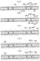
先ず、本発明の第1実施例に係る多層プリント配線板10の構成について、図1〜図7を参照して説明する。図6は、該多層プリント配線板10の断面図を、図7は、図6に示す多層プリント配線板10にICチップ90を取り付け、ドータボード94へ載置した状態を示している。図6に示すように、多層プリント配線板10では、コア基板30の表面に導体回路34、導体層34P、裏面に導体回路34、導体層34Eが形成されている。上側の導体層34Pは、電源用のプレーン層として形成され、下側の導体層34Eは、アース用のプレーン層として形成されている。コア基板30の表面と裏面とはスルーホール36を介して接続されている。更に、該導体層34P、34Eの上にバイアホール60及び導体回路58の形成された層間樹脂絶縁層50と、バイアホール160及び導体回路158の形成された層間樹脂絶縁層150とが配設されている。該バイアホール160及び導体回路158の上層にはソルダーレジスト層70が形成されており、該ソルダーレジスト層70の開口部71を介して、バイアホール160及び導体回路158にバンプ76U、76Dが形成されている。
【0036】
図7中に示すように、多層プリント配線板10の上面側のハンダバンプ76Uは、ICチップ90のランド92へ接続される。更に、チップコンデンサ98が実装される。一方、下側のハンダバンプ76Dは、ドータボード94のランド96へ接続されている。
【0037】
ここで、コア基板30上の導体層34P、34Eは、厚さ1〜250μmに形成され、層間樹脂絶縁層50上の導体回路58及び層間樹脂絶縁層150上の導体回路158は5〜25μm(望ましい範囲10〜20μm)に形成されている。
【0038】
第1実施例の多層プリント配線板では、コア基板30の電源層(導体層)34P、導体層34Eが厚くなることにより、コア基板の強度が増す、それによりコア基板自体の厚みを薄くしたとしても、反りや発生した応力を基板自体で緩和することが可能となる。
【0039】
また、導体層34P、34Eを厚くすることにより、導体自体の体積を増やすことができる。その体積を増やすことにより、導体での抵抗が低減することができる。
【0040】
更に、導体層34Pを電源層として用いることで、ICチップ90への電源の供給能力が向上させることができる。そのため、該多層プリント基板上にICチップを実装したときに、ICチップ〜基板〜電源までのループインダクタンスを低減することができる。そのために、初期動作における電源不足が小さくなるため、電源不足が起き難くなり、そのためにより高周波領域のICチップを実装したとしても、初期起動における誤動作やエラーなどを引き起こすことがない。更に、導体層34Eをアース層として用いることで、ICチップの信号、電力供給にノイズが重畳しなくなり、誤動作やエラーを防ぐことができる。
【0041】
引き続き、図6を参照して上述した多層プリント配線板10の製造方法について図1〜図5を参照して説明する。
(第1実施例−1)
A.層間樹脂絶縁層の樹脂フィルムの作製ビスフェノールA型エポキシ樹脂(エポキシ当量455、油化シェルエポキシ社製エピコート1001)29重量部、クレゾールノボラック型エポキシ樹脂(エポキシ当量215、大日本インキ化学工業社製 エピクロンN−673)39重量部、トリアジン構造含有フェノールノボラック樹脂(フェノール性水酸基当量120、大日本インキ化学工業社製 フェノライトKA−7052)30重量部をエチルジグリコールアセテート20重量部、ソルベントナフサ20重量部に攪拌しながら加熱溶解させ、そこへ末端エポキシ化ポリブタジエンゴム(ナガセ化成工業社製 デナレックスR−45EPT)15重量部と2−フェニル−4、5−ビス(ヒドロキシメチル)イミダゾール粉砕品1.5重量部、微粉砕シリカ2.5重量部、シリコン系消泡剤0.5重量部を添加しエポキシ樹脂組成物を調製した。
得られたエポキシ樹脂組成物を厚さ38μmのPETフィルム上に乾燥後の厚さが50μmとなるようにロールコーターを用いて塗布した後、80〜120℃で10分間乾燥させることにより、層間樹脂絶縁層用樹脂フィルムを作製した。
【0042】
B.樹脂充填材の調製
ビスフェノールF型エポキシモノマー(油化シェル社製、分子量:310、YL983U)100重量部、表面にシランカップリング剤がコーティングされた平均粒径が1.6μmで、最大粒子の直径が15μm以下のSiO2 球状粒子(アドテック社製、CRS 1101−CE)170重量部およびレベリング剤(サンノプコ社製 ペレノールS4)1.5重量部を容器にとり、攪拌混合することにより、その粘度が23±1℃で44〜49Pa・sの樹脂充填材を調製した。なお、硬化剤として、イミダゾール硬化剤(四国化成社製、2E4MZ−CN)6.5重量部を用いた。充填材用樹脂としては、他のエポキシ樹脂(例えば、ビスフェノールA型、ノボラック型など)、ポリイミド樹脂、フェノール樹脂などの熱硬化性樹脂を用いてもよい。
【0043】
C.多層プリント配線板の製造
(1)厚さ0.2〜0.8mmのガラスエポキシ樹脂またはBT(ビスマレイミドトリアジン)樹脂からなる絶縁性基板30の両面に5〜250μmの銅箔32がラミネートされている銅張積層板30Aを出発材料とした(図1(A))。まず、この銅張積層板をドリル削孔し、無電解めっき処理および電解めっき処理を施し、パターン状にエッチングすることにより、基板の両面に導体回路34、導体層34P、34Eとスルーホール36を形成した(図1(B))。
【0044】
(2)スルーホール36および下層導体回路34を形成した基板30を水洗いし、乾燥した後、NaOH(10g/l)、NaClO2 (40g/l)、Na3 PO4 (6g/l)を含む水溶液を黒化浴(酸化浴)とする黒化処理、および、NaOH(10g/l)、NaBH4 (6g/l)を含む水溶液を還元浴とする還元処理を行い、そのスルーホール36内に粗化面36αを形成すると共に、導体回路34、導体層34P、34Eの全表面に粗化面34αを形成した(図1(C))。
【0045】
(3)上記Bに記載した樹脂充填材を調製した後、下記の方法により調製後24時間以内に、スルーホール36内、および、基板の導体回路非形成部に樹脂充填材40の層を形成した(図1(D))。
即ち、スルーホールおよび導体回路非形成部に相当する部分が開口した版を有する樹脂充填用マスクを基板上に載置し、スキージを用いてスルーホール内、凹部となっている下層導体回路非形成部、および、下層導体回路の外縁部に樹脂充填材を充填し、100℃/20分の条件で乾燥させた。
【0046】
(4)上記(3)の処理を終えた基板の片面を、#600のベルト研磨紙(三共理化学製)を用いたベルトサンダー研磨により、導体層34P、34Eの外縁部やスルーホール36のランドの外縁部に樹脂充填材40が残らないように研磨し、次いで、上記ベルトサンダー研磨による傷を取り除くため、導体層34P、34Eの全表面(スルーホールのランド表面を含む)にバフ研磨を行った。このような一連の研磨を基板の他方の面についても同様に行った。次いで、100℃で1時間、150℃で1時間の加熱処理を行って樹脂充填材40を硬化した(図2(A))。
【0047】
このようにして、スルーホール36や導体回路非形成部に形成された樹脂充填材40の表層部および導体層34P、34Eの表面を平坦化し、樹脂充填材40と導体層34P、34Eの側面とが粗化面を介して強固に密着し、またスルーホール36の内壁面と樹脂充填材とが粗化面を介して強固に密着した基板を得た。即ち、この工程により、樹脂充填材の表面と下層導体回路の表面とが略同一平面となる。
コア基板の導体層の厚みはコア基板の導体層の厚みは1〜250μmの間で形成されて、コア基板上に形成された電源層の導体層の厚みは、1〜250μmの間で形成された。このとき、実施例1−1では、銅箔の厚み40μmのものを用いて、コア基板の導体層の厚みは30μm、コア基板上に形成された電源層の導体層の厚みは30μmであった。しかしながら、導体層の厚みは上記厚みの範囲を超えてもよい。
【0048】
(5)上記基板を水洗、酸性脱脂した後、ソフトエッチングし、次いで、エッチング液を基板の両面にスプレイで吹きつけて、導体回路34、導体層34P、34Eの表面とスルーホール36のランド表面と内壁とをエッチングすることにより、導体回路の全表面に粗化面36βを形成した(図2(B))。エッチング液としては、イミダゾール銅(II)錯体10重量部、グリコール酸7.3重量部、塩化カリウム5重量部からなるエッチング液(メック社製、メックエッチボンド)を使用した。
【0049】
(6)基板の両面に、Aで作製した基板より少し大きめの層間樹脂絶縁層用樹脂フィルム50γを基板上に載置し、圧力0.45MPa、温度80℃、圧着時間10秒の条件で仮圧着して裁断した後、さらに、以下の方法により真空ラミネーター装置を用いて貼り付けることにより層間樹脂絶縁層を形成した(図2(C))。すなわち、層間樹脂絶縁層用樹脂フィルムを基板上に、真空度67Pa、圧力0.47MPa、温度85℃、圧着時間60秒の条件で本圧着し、その後、170℃で40分間熱硬化させた。
【0050】
(7)次に、層間樹脂絶縁層上に、厚さ1.2mmの貫通孔が形成されたマスクを介して、波長10.4μmのCO2 ガスレーザにて、ビーム径4.0mm、トップハットモード、パルス幅8.1μ秒、マスクの貫通孔の径1.0mm、1ショットの条件で層間樹脂絶縁層2に、直径60〜100μmの間でのバイアホール用開口50aを形成した(図2(D))。今回は直径60μmと75μmで形成した。
【0051】
(8)バイアホール用開口6を形成した基板を、60g/lの過マンガン酸を含む80℃の溶液に10分間浸漬し、層間樹脂絶縁層2の表面に存在するエポキシ樹脂粒子を溶解除去することにより、バイアホール用開口50aの内壁を含む層間樹脂絶縁層50の表面に粗化面50αを形成した(図2(E))。
【0052】
(9)次に、上記処理を終えた基板を、中和溶液(シプレイ社製)に浸漬してから水洗いした。
さらに、粗面化処理(粗化深さ3μm)した該基板の表面に、パラジウム触媒を付与することにより、層間樹脂絶縁層の表面およびバイアホール用開口の内壁面に触媒核を付着させた。すなわち、上記基板を塩化パラジウム(PbCl2 )と塩化第一スズ(SnCl2 )とを含む触媒液中に浸漬し、パラジウム金属を析出させることにより触媒を付与した。
【0053】
(10)次に、以下の組成の無電解銅めっき水溶液中に、触媒を付与した基板を浸漬して、粗面全体に厚さ0.3〜3.0μmの無電解銅めっき膜を形成し、バイアホール用開口50aの内壁を含む層間樹脂絶縁層50の表面に無電解銅めっき膜52が形成された基板を得た(図3(A))。
〔無電解めっき水溶液〕
NiSO4 0.003 mol/l
酒石酸 0.200 mol/l
硫酸銅 0.032 mol/l
HCHO 0.050 mol/l
NaOH 0.100 mol/l
α、α′−ビピリジル 100 mg/l
ポリエチレングリコール(PEG) 0.10 g/l
〔無電解めっき条件〕
34℃の液温度で45分
【0054】
(11)無電解銅めっき膜52が形成された基板に市販の感光性ドライフィルムを張り付け、マスクを載置して、110mJ/cm2 で露光し、0.8%炭酸ナトリウム水溶液で現像処理することにより、厚さ25μmのめっきレジスト54を設けた(図3(B))。
【0055】
(12)ついで、基板を50℃の水で洗浄して脱脂し、25℃の水で水洗後、さらに硫酸で洗浄してから、以下の条件で電解めっきを施し、めっきレジスト54非形成部に、厚さ20μmの電解銅めっき膜56を形成した(図3(C))。
〔電解めっき液〕
硫酸 2.24 mol/l
硫酸銅 0.26 mol/l
添加剤 19.5 ml/l
(アトテックジャパン社製、カパラシドGL)
〔電解めっき条件〕
電流密度 1 A/dm2
時間 65 分
温度 22±2 ℃
【0056】
(13)さらに、めっきレジスト3を5%KOHで剥離除去した後、そのめっきレジスト下の無電解めっき膜を硫酸と過酸化水素との混合液でエッチング処理して溶解除去し、独立の導体回路58及びバイアホール60とした(図3(D))。
【0057】
(14)ついで、上記(5)と同様の処理を行い、導体回路58及びバイアホール60の表面に粗化面58α、60αを形成した。上層の導体回路58の厚みは15μmの厚みであった(図4(A))。ただし、上層の導体回路の厚みは、5〜25μmの間で形成してもよい。
【0058】
(15)上記(6)〜(14)の工程を繰り返すことにより、さらに上層の導体回路を形成し、多層配線板を得た(図4(B))。
【0059】
(16)次に、ジエチレングリコールジメチルエーテル(DMDG)に60重量%の濃度になるように溶解させた、クレゾールノボラック型エポキシ樹脂(日本化薬社製)のエポキシ基50%をアクリル化した感光性付与のオリゴマー(分子量:4000)45.67重量部、メチルエチルケトンに溶解させた80重量%のビスフェノールA型エポキシ樹脂(油化シェル社製、商品名:エピコート1001)16.0重量部、イミダゾール硬化剤(四国化成社製、商品名:2E4MZ−CN)1.6重量部、感光性モノマーである2官能アクリルモノマー(日本化薬社製、商品名:R604)4.5重量部、同じく多価アクリルモノマー(共栄化学社製、商品名:DPE6A)1.5重量部、分散系消泡剤(サンノプコ社製、S−65)0.71重量部を容器にとり、攪拌、混合して混合組成物を調製し、この混合組成物に対して光重合開始剤としてベンゾフェノン(関東化学社製)1.8重量部、光増感剤としてのミヒラーケトン(関東化学社製)0.2重量部、を加えることにより、粘度を25℃で2.0Pa・sに調整したソルダーレジスト組成物を得た。
なお、粘度測定は、B型粘度計(東京計器社製、DVL−B型)で60min-1の場合はローターNo.4、6min-1の場合はローターNo.3によった。
【0060】
(17)次に、多層配線基板の両面に、上記ソルダーレジスト組成物70を20μmの厚さで塗布し、70℃で20分間、70℃で30分間の条件で乾燥処理を行った後(図4(C))、ソルダーレジスト開口部のパターンが描画された厚さ5mmのフォトマスクをソルダーレジスト層70に密着させて1000mJ/cm2 の紫外線で露光し、DMTG溶液で現像処理し、200μmの直径の開口71を形成した(図5(A))。
そして、さらに、80℃で1時間、100℃で1時間、120℃で1時間、150℃で3時間の条件でそれぞれ加熱処理を行ってソルダーレジスト層を硬化させ、開口を有し、その厚さが15〜25μmのソルダーレジストパターン層を形成した。上記ソルダーレジスト組成物としては、市販のソルダーレジスト組成物を使用することもできる。
【0061】
(18)次に、ソルダーレジスト層70を形成した基板を、塩化ニッケル(2.3×10⁻¹mol/l)、次亜リン酸ナトリウム(2.8×10-1mol/l)、クエン酸ナトリウム(1.6×10-1mol/l)を含むpH=4.5の無電解ニッケルめっき液に20分間浸漬して、開口部71に厚さ5μmのニッケルめっき層72を形成した。さらに、その基板をシアン化金カリウム(7.6×10-3mol/l)、塩化アンモニウム(1.9×10-1mol/l)、クエン酸ナトリウム(1.2×10-1mol/l)、次亜リン酸ナトリウム(1.7×10-1mol/l)を含む無電解金めっき液に80℃の条件で7.5分間浸漬して、ニッケルめっき層72上に、厚さ0.03μmの金めっき層74を形成した(図5(B))。ニッケル−金層以外にも、スズ、貴金属層(金、銀、パラジウム、白金など)の単層を形成してもよい。
【0062】
(19)この後、基板のICチップを載置する面のソルダーレジスト層70の開口71に、スズ−鉛を含有するはんだペーストを印刷し、さらに他方の面のソルダーレジスト層の開口にスズ−アンチモンを含有するはんだペーストを印刷した後、200℃でリフローすることによりはんだバンプ(はんだ体)を形成し、はんだバンプ76U、76Dを有する多層プリント配線板を製造した(図6)。
【0063】
半田バンプ76Uを介してICチップ90を取り付け、チップコンデンサ98を実装する。そして、半田バンプ76Dを介してドータボード94へ取り付ける(図7)。
【0064】
(第1実施例−2)
図6を参照して上述した第1実施例−1と同様であるが以下の様に製造した。
コア基板の導体層の厚み:55μm コア基板の電源層の厚み:55μm
層間絶縁層の導体層の厚み:15μm
【0065】
(第1実施例−3)
第1実施例−1と同様であるが、以下のように製造した。
コア基板の導体層の厚み:75μm コア基板の電源層の厚み:75μm
層間絶縁層の導体層の厚み:15μm
【0066】
(第1実施例−4)
第1実施例と同様であるが、以下のように製造した。
コア基板の導体層の厚み:180μm コア基板の電源層の厚み:180μm
層間絶縁層の導体層の厚み:6μm
【0067】
(第1実施例−5)
第1実施例と同様であるが、以下のように製造した。
コア基板の導体層の厚み:18μm コア基板の電源層の厚み:18μm
層間絶縁層の導体層の厚み:15μm
【0068】
なお、第1実施例において、1<(コア基板の電源層の導体層の厚み/層間絶縁層の導体層の厚み)≦40のものを適合例として、(コア基板の電源層の導体層の厚み/層間絶縁層の導体層の厚み)≦1を比較例とした。また、(コア基板の電源層の導体層の厚み/層間絶縁層の導体層の厚み)>40のものを参考例とした。
【0069】
[第2実施例]セラミック基板
第2実施例に係る多層プリント配線板について説明する。
図6を参照して上述した第1実施例では、コア基板が絶縁樹脂で形成されていた。これに対して、第2実施例では、コア基板がセラミック、ガラス、ALN、ムライトなどからなる無機系硬質基板であるが、他の構成は図6を参照して上述した第1実施例と同様であるため、図示及び説明は省略する。
【0070】
第2実施例の多層プリント配線板においても、コア基板30上の導体層34P、34P及びコア基板内の導体層24は、銅、タングステムなどの金属で形成され、層間樹脂絶縁層50上の導体回路58及び層間樹脂絶縁層150上の導体回路158は銅で形成されている。この第2実施例においても第1実施例と同様な効果を得ている。このとき、コア基板の導体層の厚み、コア基板の電源層の厚み、層間絶縁層の厚みも第1実施例と同様に形成された。また、第2実施例において、1<(コア基板の電源層の導体層の厚み/層間絶縁層の導体層の厚み)≦40のものを適合例として、(コア基板の電源層の導体層の厚み/層間絶縁層の導体層の厚み)≦1を比較例とした。また、(コア基板の電源層の導体層の厚み/層間絶縁層の導体層の厚み)>40のものを参考例とした。
【0071】
(第2実施例−1)
上述した第2実施例と同様であるが以下の様に製造した。
コア基板の導体層の厚み:30μm コア基板の電源層の厚み:30μm
層間絶縁層の導体層の厚み:15μm
【0072】
(第2実施例−2)
上述した第2実施例と同様であるが以下の様に製造した。
コア基板の導体層の厚み:50μm コア基板の電源層の厚み:50μm
層間絶縁層の導体層の厚み:15μm
【0073】
(第2実施例−3)
上述した第2実施例と同様であるが以下の様に製造した。
コア基板の導体層の厚み:75μm コア基板の電源層の厚み:75μm
層間絶縁層の導体層の厚み:15μm
【0074】
(第2実施例−4)
上述した第2実施例と同様であるが以下の様に製造した。
コア基板の導体層の厚み:180μm コア基板の電源層の厚み:180μm
層間絶縁層の導体層の厚み:6μm
【0075】
[第3実施例]金属コア基板
図8及び図9を参照して第3実施例に係る多層プリント配線板について説明する。
図6を参照して上述した第1実施例では、コア基板が樹脂板で形成されていた。これに対して、第3実施例では、コア基板が金属板から成る。
【0076】
図8は、第3実施例に係る多層プリント配線板10の断面図を、図9は、図8に示す多層プリント配線板10にICチップ90を取り付け、ドータボード94へ載置した状態を示している。図8に示すように、多層プリント配線板10では、コア基板30は金属板からなり、電源層として用いられる。コア基板30の両面には、バイアホール60及び導体回路58が配置された層間樹脂絶縁層50が形成され、層間樹脂絶縁層50の上には、バイアホール160及び導体回路158が配置された層間樹脂絶縁層150が形成されている。コア基板30の通孔33内には、スルーホール36が形成され、バイアホールの両端には蓋めっき層37が配置されている。該バイアホール160及び導体回路158の上層にはソルダーレジスト層70が形成されており、該ソルダーレジスト層70の開口部71を介して、バイアホール160及び導体回路158にバンプ76U、76Dが形成されている。
【0077】
図9中に示すように、多層プリント配線板10の上面側のハンダバンプ76Uは、ICチップ90のランド92へ接続される。更に、チップコンデンサ98が実装される。一方、下側のハンダバンプ76Dは、ドータボード94のランド96へ接続されている。
【0078】
ここで、コア基板30は、200〜600μmに形成されている。金属板の厚みは、15〜300μmの間で形成された。層間絶縁層の導体層の厚みは、5〜25μmの間で形成してもよい。しかしながら、金属層の厚みは上述の範囲を超えてもよい。
この第3実施例においても、第1実施例と同様な効果を得ている。
【0079】
(第3実施例−1)
図8を参照して上述した第3実施例と同様であるが以下のように設定した。
コア基板の厚み:550μm コア基板の電源層の厚み:35μm
層間絶縁層の導体層の厚み:15μm
【0080】
(第3実施例−2)
第3実施例と同様であるが以下のように設定した。
コア基板の厚み:600μm コア基板の電源層の厚み:55μm
層間絶縁層の導体層の厚み:15μm
【0081】
(第3実施例−3)
第3実施例と同様であるが以下のように設定した。
コア基板の厚み:550μm コア基板の電源層の厚み:100μm
層間絶縁層の導体層の厚み:10μm
【0082】
(第3実施例−4)
第3実施例と同様であるが以下のように設定した。
コア基板の厚み:550μm コア基板の電源層の厚み:180μm
層間絶縁層の導体層の厚み:6μm
【0083】
(第3実施例−5)
第3実施例と同様であるが以下のように設定した。
コア基板の厚み:550μm コア基板の電源層の厚み:240μm
層間絶縁層の導体層の厚み:6μm
【0084】
なお、第3実施例において、1<(コア基板の電源層の導体層の厚み/層間絶縁層の導体層の厚み)≦40のものを適合例として、(コア基板の電源層の導体層の厚み/層間絶縁層の導体層の厚み)≦1を比較例とした。また、(コア基板の電源層の導体層の厚み/層間絶縁層の導体層の厚み)>40のものを参考例とした。
【0085】
[第4実施例]多層コア基板
図10及び図11を参照して第4実施例に係る多層プリント配線板について説明する。
図6を参照して上述した第1実施例では、コア基板が単板で形成されていた。これに対して、第4実施例では、コア基板が積層板からなり、積層板内に導体層が設けられている。
【0086】
図10は、第4実施例に係る多層プリント配線板10の断面図を、図11は、図10に示す多層プリント配線板10にICチップ90を取り付け、ドータボード94へ載置した状態を示している。図10に示すように、多層プリント配線板10では、コア基板30の表面及び裏面に導体回路34、導体層34Pが形成され、コア基板30内に導体層24が形成されている。導体層34P及び導体層24は、電源用のプレーン層として形成されている。導体層34Pと導体層24とは導電ポスト26により接続されている。(この場合の導電ポストとは、スルーホール、非貫通孔などのバイアホール(含むブラインドスルーホール、ブラインドバイアホール)スルーホールもしくはバイアホール導電性材料で充填したもの意味する。)更に、該導体層34Pの上にバイアホール60及び導体回路58の形成された層間樹脂絶縁層50と、バイアホール160及び導体回路158の形成された層間樹脂絶縁層150とが配置されている。該バイアホール160及び導体回路158の上層にはソルダーレジスト層70が形成されており、該ソルダーレジスト層70の開口部71を介して、バイアホール160及び導体回路158にバンプ76U、76Dが形成されている。
【0087】
図11中に示すように、多層プリント配線板10の上面側のハンダバンプ76Uは、ICチップ90のランド92へ接続される。更に、チップコンデンサ98が実装される。一方、下側のハンダバンプ76Dは、ドータボード94のランド96へ接続されている。
【0088】
ここで、コア基板30上の導体回路34、導体層34P、34P及びコア基板内の導体層24が形成され、層間樹脂絶縁層50上の導体回路58及び層間樹脂絶縁層150上の導体回路158が形成されている。コア基板の導体層34Pおよび導体層24の厚みはコア基板の導体層の厚みは1〜250μmの間で形成されて、コア基板上に形成された電源層としての役目を果たすの導体層の厚みは、1〜250μmの間で形成された。この場合の導体層の厚みは、コア基板の電源層の厚みの総和である。内層である導体層34、表層である導体層24、その双方を足したものであるという意味である。信号線の役目を果たしているものとを足すことではない。この第4実施例においても、3層の導体層34P、34P、24の厚みを合わせることで、第1実施例と同様な効果を得ている。電源層の厚みは上述の範囲を超えてもよい。
なお、第4実施例において、1<(コア基板の電源層の導体層の厚みの総和/層間絶縁層の導体層の厚み)≦40のものを適合例として、(コア基板の電源層の導体層の厚みの総和/層間絶縁層の導体層の厚み)≦1を比較例とした。(コア基板の電源層の導体層の厚みの総和/層間絶縁層の導体層の厚み)>40のものを参考例とした。
【0089】
(第4実施例−1)
図10を参照して上述した第4実施例と同様であるが以下のように設定した。
コア基板の導体層(電源層)の厚み:15μm
中間導体層(電源層)の厚み:20μm
コア基板の電源層の厚みの和:50μm
層間絶縁層の導体層の厚み:15μm
【0090】
(第4実施例−2)
第4実施例と同様であるが、以下のように製造した。
コア基板の導体層(電源層)の厚み:20μm
中間導体層(電源層)の厚み:20μm
コア基板の電源層の厚みの和:60μm
層間絶縁層の導体層の厚み:15μm
【0091】
(第4実施例−3)
第4実施例と同様であるが、以下のように製造した。
コア基板の導体層(電源層)の厚み:25μm
中間導体層(電源層)の厚み:25μm
コア基板の電源層の厚みの和:75μm
層間絶縁層の導体層の厚み:15μm
【0092】
(第4実施例−4)
第4実施例と同様であるが、以下のように製造した。
コア基板の導体層(電源層)の厚み:50μm
中間導体層(電源層)の厚み:100μm
コア基板の電源層の厚みの和:200μm
層間絶縁層の導体層の厚み:10μm
【0093】
(第4実施例−5)
第4実施例と同様であるが、以下のように製造した。
コア基板の導体層(電源層)の厚み:55μm
中間導体層(電源層)の厚み:250μm
コア基板の電源層の厚みの和:360μm
層間絶縁層の導体層の厚み:12μm
【0094】
(第4実施例−6)
第4実施例と同様であるが、以下のように製造した。
コア基板の導体層(電源層)の厚み:55μm
中間導体層(電源層)の厚み:250μm
コア基板の電源層の厚みの和:360μm
層間絶縁層の導体層の厚み:9μm
【0095】
[第5実施例] 多層コア基板
図12〜図20を参照して本発明の第5実施例に係る多層プリント配線板について説明する。
先ず、第5実施例に係る多層プリント配線板10の構成について、図19、図20を参照して説明する。図19は、該多層プリント配線板10の断面図を、図20は、図19に示す多層プリント配線板10にICチップ90を取り付け、ドータボード94へ載置した状態を示している。図19に示すように、多層プリント配線板10では多層コア基板30を用いている。多層コア基板30の表面側に導体回路34、導体層34P、裏面に導体回路34、導体層34Eが形成されている。上側の導体層34Pは、電源用のプレーン層として形成され、下側の導体層34Eは、アース用のプレーン層として形成されている。更に、多層コア基板30の内部の表面側に、内層の導体回路16、導体層16E、裏面に導体回路16、導体層16Pが形成されている。上側の導体層16Eは、アース用のプレーン層として形成され、下側の導体層16Pは、電源用のプレーン層として形成されている。電源用のプレーン層との接続は、スルーホールやバイアホールにより行われる。プレーン層は、片側だけの単層であっても、2層以上に配置したものでもよい。2層〜4層で形成されることが望ましい。4層以上では電気的な特性の向上が確認されていないことからそれ以上多層にしてもその効果は4層と同等程度である。特に、2層で形成されることが、多層コア基板の剛性整合という点において基板の伸び率が揃えられるので反りが出にくいからである。多層コア基板30の中央には、電気的に隔絶された金属板12が収容されている。(該金属板12は、心材としての役目も果たしているが、スルーホールやバイアホールなどどの電気な接続がされていない。主として、基板の反りに対する剛性を向上させているのである。)該金属板12に、絶縁樹脂層14を介して表面側に、内層の導体回路16、導体層16E、裏面に導体回路16、導体層16Pが、更に、絶縁樹脂層18を介して表面側に導体回路34、導体層34Pが、裏面に導体回路34、導体層34Eが形成されている。多層コア基板30は、スルーホール36を介して表面側と裏面側との接続が取られている。
【0096】
多層コア基板30の表面の導体層34P、34Eの上には、バイアホール60及び導体回路58の形成された層間樹脂絶縁層50と、バイアホール160及び導体回路158の形成された層間樹脂絶縁層150とが配設されている。該バイアホール160及び導体回路158の上層にはソルダーレジスト層70が形成されており、該ソルダーレジスト層70の開口部71を介して、バイアホール160及び導体回路158にバンプ76U、76Dが形成されている。
【0097】
図20中に示すように、多層プリント配線板10の上面側のハンダバンプ76Uは、ICチップ90のランド92へ接続される。更に、チップコンデンサ98が実装される。一方、下側の外部端子76Dは、ドータボード94のランド96へ接続されている。この場合における外部端子とは、PGA、BGA,半田バンプ等を指している。
【0098】
ここで、コア基板30表層の導体層34P、34Eは、厚さ10〜60μmに形成され、内層の導体層16P、16Eは、厚さ10〜250μmに形成され、層間樹脂絶縁層50上の導体回路58及び層間樹脂絶縁層150上の導体回路158は10〜25μmに形成されている。
【0099】
第5実施例の多層プリント配線板では、コア基板30の表層の電源層(導体層)34P、導体層34、内層の電源層(導体層)16P、導体層16Eおよび金属板12を厚くすることにより、コア基板の強度が増す。それによりコア基板自体を薄くしたとしても、反りや発生した応力を基板自体で緩和することが可能となる。
【0100】
また、導体層34P、34E、導体層16P、16Eを厚くすることにより、導体自体の体積を増やすことができる。その体積を増やすことにより、導体での抵抗を低減することができる。
【0101】
更に、導体層34P、16Pを電源層として用いることで、ICチップ90への電源の供給能力が向上させることができる。そのため、該多層プリント基板上にICチップを実装したときに、ICチップ〜基板〜電源までのループインダクタンスを低減することができる。そのために、初期動作における電源不足が小さくなるため、電源不足が起き難くなり、そのためにより高周波領域のICチップを実装したとしても、初期起動における誤動作やエラーなどを引き起こすことがない。更に、導体層34E、16Eをアース層として用いることで、ICチップの信号、電力供給にノイズが重畳しなくなり、誤動作やエラーを防ぐことができる。コンデンサを実装することにより、コンデンサ内の蓄積されている電源を補助的に用いることができるので、電源不足を起しにくくなる。特に、ICチップの直下に配設させることにより、その効果(電源不足を起しにくくする)は顕著によくなる。その理由として、ICチップの直下であれば、多層プリント配線板での配線長を短くすることができるからである。
【0102】
第5実施例では、多層コア基板30は、内層に厚い導体層16P、16Eを、表面に薄い導体層34P、34Eを有し、内層の導体層16P、16Eと表面の導体層34P、34Eとを電源層用の導体層、アース用の導体層として用いる。即ち、内層側に厚い導体層16P、16Eを配置しても、導体層を覆う樹脂層が形成されている。そのために、導体層が起因となって凹凸を相殺させることで多層コア基板30の表面を平坦にすることができる。このため、層間絶縁層50、150の導体層58、158にうねりを生じせしめないように、多層コア基板30の表面に薄い導体層34P、34Eを配置しても、内層の導体層16P、16Eと足した厚みでコアの導体層として十分な厚みを確保することができる。うねりが生じないために、層間絶縁層上の導体層のインピーダンスに不具合が起きない。導体層16P、34Pを電源層用の導体層として、導体層16E、34Eをアース用の導体層として用いることで、多層プリント配線板の電気特性を改善することが可能になる。
【0103】
更に、コア基板内で導体層34Pと導体層16Pとの間の信号線16(導体層16Eと同層)を配置することでマイクロストリップ構造を形成させることができる。同様に、導体層16Eと導体層34Eとの間の信号線16(導体層16Pと同層)を配置することでマイクロストリップ構造を形成させることができる。マイクロストリップ構造を形成させることにより、インダクタンスも低下し、インピーダンス整合を取ることができるのである。そのために、電気特性も安定化することができる。
【0104】
即ち、コア基板の内層の導体層16P、16Eの厚みを、層間絶縁層50、150上の導体層58、158よりも厚くする。これにより、多層コア基板30の表面に薄い導体層34E、34Pを配置しても、内層の厚い導体層16P、16Eと足すことで、コアの導体層として十分な厚みを確保できる。その比率は、1<(コアの内層の導体層/層間絶縁層の導体層)≦40であることが望ましい。1.2≦(コアの内層の導体層/層間絶縁層の導体層)≦30であることがさらに望ましい。
【0105】
多層コア基板30は、電気的に隔絶された金属板12の両面に、樹脂層14を介在させて内層の導体層16P、16Eが、更に、当該内層の導体層16P、16Eの外側に樹脂層18を介在させて表面の導体層34P、34Eが形成されて成る。中央部に電気的に隔絶された金属板12を配置することで、十分な機械的強度を確保することができる。更に、金属板12の両面に樹脂層14を介在させて内層の導体層16P、16Eを、更に、当該内層の導体層16P、16Eの外側に樹脂層18を介在させて表面の導体層34P、34Eを形成することで、金属板12の両面で対称性を持たせ、ヒートサイクル等において、反り、うねりが発生することを防げる。
【0106】
図21は、第5実施例の改変例を示している。この改変例では、ICチップ90の直下にコンデンサ98を配置してある。このため、ICチップ90とコンデンサ98との距離が近く、ICチップ90へ供給する電源の電圧降下を防ぐことができる。
【0107】
引き続き、図19に示す多層プリント配線板10の製造方法について図12〜図18を参照して説明する。
(1)金属層の形成
図12(A)に示す厚さ50〜400μmの間の内層金属層(金属板)12に、表裏を買通する開口12aを設ける(図12(B))。金属層の材質としては、銅、ニッケル、亜鉛、アルミニウム、鉄などの金属が配合されているものを用いることができる。開口12aは、パンチング、エッチング、ドリリング、レーザなどによって穿設する。場合によっては、開口12aを形成した金属層12の全面に電解めっき、無電解めっき、置換めっき、スパッタによって、金属膜13を被覆してもよい(図12(C))。なお、金属板12は、単層でも、2層以上の複数層でもよい。また、金属膜13は、開口12aの角部において、曲面を形成するほうが望ましい。それにより、応力の集中するポイントがなくなり、その周辺でのクラックなどの不具合が引き起こしにくい。
【0108】
(2)内層絶縁層の形成
金属層12の全体を覆い、開口12a内を充填するために、絶縁樹脂を用いる。形成方法としては、例えば、厚み30〜200μm程度のBステージ状の樹脂フィルムを金属板12で挟んでから、熱圧着してから硬化させ絶縁樹脂層14を形成することができる(図12(D))。場合によっては、塗布、塗布とフィルム圧着の混合、もしくは閑口部分だけを塗布して、その後、フィルムで形成してもよい。
材料としては、ポリイミド樹脂、エポキシ樹脂、フェノール樹脂、BT樹脂等の熱硬化性樹脂をガラスクロス等の心材に含浸させたプリプレグを用いることが望ましい。それ以外にも樹脂を用いてもよい。
【0109】
(3)金属箔の貼り付け
樹脂層14で覆われた金属層12の両面に、内層金属層16αを形成させる(図12(E))。その一例として、厚み12〜275μmの金属箔を積層させた。金属箔を形成させる以外の方法として、片面銅張積層板を積層させる。金属箔上に、めっきなどで形成される。
【0110】
(4)内層金属層の回路形成
2層以上にしてもよい。アディティブ法により金属層を形成してもよい。
テンティング法、エッチング工程等を経て、内層金属層16αから内層導体層16、16P、16Eを形成させた(図12(F))。このときの内層導体層の厚みは、10〜250μmで形成させた。しかしながら、上述の範囲を超えてもよい。
【0111】
(5)外層絶縁層の形成
内層導体層16、16P、16Eの全体を覆い、および外層金属その回路間の隙間を充填するために、絶縁樹脂を用いる。形成方法としては、例えば、厚み30〜200μm程度のBステージ状の樹脂フィルムを金属板で挟んでから、熱圧着してから硬化させ、外層絶縁樹脂層18を形成する(図13(A))。場合によっては、塗布、塗布とフィルム圧着の混合、もしくは開口部分だけを塗布して、その後、フィルムで形成してもよい。加圧することで表面を平坦にすることができる。
【0112】
(6)最外層の金属箔の貼り付け
外層絶縁樹脂層18で覆われた基板の両面に、最外層の金属層34βを形成させる(図13(B))。その一例として、厚み10〜275μmの金属箔を積層させる。金属箔を形成させる以外の方法として、片面銅張積層板を積層させる。金属箔上に、めっきなどで2層以上にしてもよい。アディティブ法により金属層を形成してもよい。
【0113】
(7)スルーホール形成
基板の表裏を貫通する開口径50〜400μmのスルーホール用通孔36αを形成する(図13(C))。形成方法としては、ドリル、レーザもしくはレーザとドリルの複合により形成させる(最外層の絶縁層の開口をレーザで行い、場合によっては、そのレーザでの開口をターゲットマークとして用いて、その後、ドリルで開口して貫通させる)。形状としては、直線状の側壁を有するものであることが望ましい。場合によっては、テーパ状であってもよい。
【0114】
スルーホールの導電性を確保するために、スルーホール用通孔36α内にめっき膜22を形成し、表面を粗化した後(図13(D))、充填樹脂23を充填することが望ましい(図13(E))。充填樹脂としては、電気的な絶縁されている樹脂材料、(例えば 樹脂成分、硬化剤、粒子等が含有されているもの)、金属粒子による電気的な接続を行っている導電性材料(例えば、金、銅などの金属粒子、樹脂材料、硬化剤などが含有されているもの。)のいずれかを用いることができる。
めっきとしては、電解めっき、無電解めっき、パネルめっき(無電解めっきと電解めっき)などを用いることができる。金属としては、銅、ニッケル、コバルト、リン、等が含有してもので形成されるのである。めっき金属の厚みとしては、5〜30μmの間で形成されることが望ましい。
【0115】
スルーホール用通孔36α内に充填する充填樹脂23は、樹脂材料、硬化剤、粒子などからなるものを絶縁材料を用いることが望ましい。粒子としては、シリカ、アルミナなどの無機粒子、金、銀、銅などの金属粒子、樹脂粒子などの単独もしくは複合で配合させる。粒径が0.1〜5μmのものを同一径もしくは、複合径のもの混ぜたものを用いることができる。樹脂材料としては、エポキシ樹脂(例えば、ビスフェノール型エポキシ樹脂、ノボラック型エポキシ樹脂など)、フェノール樹脂などの熱硬化性樹脂、感光性を有する紫外線硬化樹脂、熱可塑性樹脂などが単一もしくは混合したものを用いることができる。硬化剤としては、イミダゾール系硬化剤、アミン系硬化剤などを用いることができる。それ以外にも、硬化安定剤、反応安定剤、粒子等を含まれていてもよい。導電性材料を用いてもよい。この場合は、金属粒子、樹脂成分、硬化剤などからなるものが導電性材料である導電性ペーストとなる。場合によっては、半田、絶縁樹脂などの絶縁材料の表層に導電性を有する金属膜を形成したものなどを用いてもよい。めっきでスルーホール用通孔36α内を充填することも可能である。導電性ペーストは硬化収縮がなされるので、表層に凹部を形成してしまうことがあるからである。
【0116】
(8)最外層の導体回路の形成
全体にめっき膜を被覆することで、スルーホール36の直上に蓋めっき25を形成してもよい(図14(A))。その後、テンティング法、エッチング工程等を経て、外層の導体回路34、34P、34Eを形成する(図14(B))。これにより、多層コア基板30を完成する。
このとき、図示されていないが多層コア基板の内層の導体層16等との電気接続を、バイアホールやブラインドスルーホール、ブラインドバイアホールにより行ってもよい。
【0117】
その後の製造方法は、図1(C)〜図5を参照して上述した第1実施例と同様に、多層コア基板30に層間樹脂絶縁層50、150、導体回路58、158を形成する。
【0118】
(9)導体回路34を形成した多層コア基板30を黒化処理、および、還元処理を行い、導体回路34、導体層34P、34Eの全表面に粗化面34βを形成する(図14(C))。
【0119】
(10)多層コア基板30の導体回路非形成部に樹脂充填材40の層を形成する(図15(A))。
【0120】
(11)上記処理を終えた基板の片面を、ベルトサンダー等の研磨により、導体層34P、34Eの外縁部に樹脂充填材40が残らないように研磨し、次いで、上記研磨による傷を取り除くため、導体層34P、34Eの全表面(スルーホールのランド表面を含む)にバフ等でさらに研磨を行った。このような一連の研磨を基板の他方の面についても同様に行った。次いで、100℃で1時間、150℃で1時間の加熱処理を行って樹脂充填材40を硬化した(図15(B))。
また、導体回路間の樹脂充填を行わなくてもよい。この場合は、層間絶縁層などの樹脂層で絶縁層の形成と導体回路間の充填を行う。
【0121】
(12)上記多層コア基板30に、エッチング液を基板の両面にスプレイで吹きつけて、導体回路34、導体層34P、34Eの表面とスルーホール36のランド表面と内壁とをエッチング等により、導体回路の全表面に粗化面36βを形成した(図15(C))。
【0122】
(13)多層コア基板30の両面に、層間樹脂絶縁層用樹脂フィルム50γを基板上に載置し、仮圧着して裁断した後、さらに、真空ラミネーター装置を用いて貼り付けることにより層間樹脂絶縁層を形成した(図16(A))。
【0123】
(14)次に、層間樹脂絶縁層上に、厚さ1.2mmの貫通孔が形成されたマスクを介して、波長10.4μmのCO2 ガスレーザにて、ビーム径4.0mm、トップハットモード、パルス幅7.9μ秒、マスクの貫通孔の径1.0mm、1ショットの条件で層間樹脂絶縁層2に、直径80μmのバイアホール用開口50aを形成した(図16(B))。
【0124】
(15)多層コア基板30を、60g/lの過マンガン酸を含む80℃の溶液に10分間浸漬し、バイアホール用開口50aの内壁を含む層間樹脂絶縁層50の表面に粗化面50αを形成した(図15(C))。粗化面は0.1〜5μmの間で形成した。
【0125】
(16)次に、上記処理を終えた多層コア基板30を、中和溶液(シプレイ社製)に浸漬してから水洗いした。さらに、粗面化処理(粗化深さ3μm)した該基板の表面に、パラジウム触媒を付与することにより、層間樹脂絶縁層の表面およびバイアホール用開口の内壁面に触媒核を付着させた。
【0126】
(17)次に、無電解銅めっき水溶液中に、触媒を付与した基板を浸漬して、粗面全体に厚さ0.6〜3.0μmの無電解銅めっき膜を形成し、バイアホール用開口50aの内壁を含む層間樹脂絶縁層50の表面に無電解銅めっき膜52が形成された基板を得る(図15(D))。
【0127】
(18)無電解銅めっき膜52が形成された基板に市販の感光性ドライフィルムを張り付け、マスクを載置して、現像処理することにより、めっきレジスト54を設けた(図17(A))。めっきレジストの厚みは、10〜30μmの間を用いた。
【0128】
(19)ついで、多層コア基板30に電解めっきを施し、めっきレジスト54非形成部に、厚さ5〜20μmの電解銅めっき膜56を形成した(図17(B))。
【0129】
(20)さらに、めっきレジストを5%程度のKOHで剥離除去した後、そのめっきレジスト下の無電解めっき膜を硫酸と過酸化水素との混合液でエッチング処理して溶解除去し、独立の導体回路58及びバイアホール60とした(図17(C))。
【0130】
(21)ついで、上記(12)と同様の処理を行い、導体回路58及びバイアホール60の表面に粗化面58α、60αを形成した。上層の導体回路58の厚みは5〜25μmで形成された。今回の厚みは15μmの厚みであった(図17(D))。
【0131】
(22)上記(14)〜(21)の工程を繰り返すことにより、さらに上層の導体回路を形成し、多層配線板を得た(図18(A))。
【0132】
(23)次に、多層配線基板の両面に、ソルダーレジスト組成物70を12〜30μmの厚さで塗布し、70℃で20分間、70℃で30分間の条件で乾燥処理を行った後(図18(B))、ソルダーレジスト開口部のパターンが描画された厚さ5mmのフォトマスクをソルダーレジスト層70に密着させて1000mJ/cm2 の紫外線で露光し、DMTG溶液で現像処理し、200μmの直径の開口71を形成した(図18(C))。
そして、さらに、80℃で1時間、100℃で1時間、120℃で1時間、150℃で3時間の条件でそれぞれ加熱処理を行ってソルダーレジスト層を硬化させ、開口を有し、その厚さが10〜25μmのソルダーレジストパターン層を形成した。
【0133】
(24)次に、ソルダーレジスト層70を形成した基板を、無電解ニッケルめっき液に浸漬して、開口部71に厚さ5μmのニッケルめっき層72を形成した。さらに、その基板を無電解金めっき液に浸漬して、ニッケルめっき層72上に、厚さ0.03μmの金めっき層74を形成した(図18(D))。ニッケル−金層以外にも、スズ、貴金属層(金、銀、パラジウム、白金など)の単層を形成してもよい。
【0134】
(25)この後、基板のICチップを載置する面のソルダーレジスト層70の開口71に、スズ−鉛を含有する半田ペーストを印刷し、さらに他方の面のソルダーレジスト層の開口にスズ−アンチモンを含有する半田ペーストを印刷した後、200℃でリフローすることにより外部端子を形成し、はんだバンプを有する多層プリント配線板を製造した(図19)。
【0135】
半田バンプ76Uを介してICチップ90を取り付け、チップコンデンサ98を実装する。そして、外部端子76Dを介してドータボード94へ取り付ける(図20)。
また、第5実施例において、1<(コア基板の電源層の厚み/層間絶縁層の導体層の厚み)≦40のものを適合例として、(コア基板の電源層の厚み/層間絶縁層の導体層の厚み)≦1を比較例とした。(コア基板の電源層の厚み/層間絶縁層の導体層の厚み)>40のものを参考例とした。
【0136】
(第5実施例−1)
図19を参照して上述した第5実施例と同様であるが以下のように設定した。
コア基板の内層の導体層の厚み:50μm 表層の導体層の厚み:20μm
コア基板の導体回路の厚みの和:100μm
層間絶縁層の導体層の厚み:15μm
内層の導体層と表層の導体層で、電源層の役目を果たした。しかしながら、表層の導体層の面積は、ランド程度のものであったので、内層の導体層と比較すると面積が小さかったので、電源を降下させる効果は相殺されてしまった。そのために、コア基板の導体層の厚みの和は、内層の2層の導体層を足したものである。
【0137】
(第5実施例−2)
内層の導体層と表層の導体層で、電源層の役目を果たした。表層、内層の各一層ずつでのスルーホールにより、電気的な接続がなされた。
コア基板の内層の導体層の厚み:60μm 外層の導体層の厚み:20μm
コア基板の導体回路の厚みの和:80μm
層間絶縁層の導体層の厚み:15μm
内層の導体層と表層の導体層で、各1層ずつ電源層の役目を果たした。表層の導体層の面積は、内層の導体層の面積同じだった。電源を降下させる効果を有する。そのために、コア基板の導体層の厚みの和は、内層の導体層と表層の導体層を足したものである。
【0138】
(第5実施例−3)
内層の導体層と表層の導体層で、電源層の役目を果たした。表層、内層の各一層ずつでのスルーホールにより、電気的な接続がなされた。
コア基板の内層の導体層の厚み:75μm 外層の導体層の厚み:20μm
コア基板の導体回路の厚みの和:150μm
層間絶縁層の導体層の厚み:15μm
内層の導体層と表層の導体層で、電源層の役目を果たした。しかしながら、表層の導体層の面積は、ランド程度のものであったので、内層の導体層と比較すると面積が小さかったので、電源を降下させる効果は相殺されてしまった。そのために、コア基板の導体層の厚みの和は、内層1層の導体層の厚みである。
【0139】
(第5実施例−4)
第5実施例−3と同様であるが、以下のように製造した。
コア基板の内層の導体層(電源層)の厚み:200μm
表層の導体層(電源層)の厚み:20μm
コア基板の導体回路の厚みの和:200μm
層間絶縁層の導体層の厚み:10μm
コア基板の導体回路の厚みの和は、内層の層の導体層を足したものである。
【0140】
(第5実施例−5)
第5実施例−3と同様であるが、以下のように製造した。
コア基板の内層の導体層(電源層)の厚み:240μm
表層の導体層(電源層)の厚み:20μm
コア基板の導体回路の厚みの和:240μm
層間絶縁層の導体層の厚み:8μm
コア基板の導体回路の厚みの和は、内層の層の導体層を足したものである。
【0141】
(第5実施例−6)
第5実施例−2と同様であるが、以下のように製造した。
コア基板の内層の導体層(電源層)の厚み:250μm
表層の導体層(電源層)の厚み:25μm
コア基板の導体回路の厚みの和:300μm
層間絶縁層の導体層の厚み:7.5μm
【0142】
[第6実施例]コンデンサ内蔵コア基板
図22及び図23を参照して第6実施例に係る多層プリント配線板について説明する。
第6実施例の多層プリント配線板では、コア基板30にチップコンデンサ20が内蔵されている。
【0143】
図22は、第6実施例に係る多層プリント配線板10の断面図を、図23は、図22に示す多層プリント配線板10にICチップ90を取り付けた状態を示している。図22に示すように、多層プリント配線板10では、コア基板30が樹脂基板30A及び樹脂層30Bからなる。樹脂基板30Aにはコンデンサ20を収容するための開口31aが設けられている。コンデンサ20の電極は、樹脂層30Bに設けられたバイアホール33により接続が取られている。コア基板30の上面には、導体回路34及び電源層を形成する導体層34Pが形成され、また、コア基板30の両面には、バイアホール60及び導体回路58が配置された層間樹脂絶縁層50が形成されている。コア基板30には、スルーホール36が形成されている。層間樹脂絶縁層50の上層にはソルダーレジスト層70が形成されており、該ソルダーレジスト層70の開口部71を介して、バイアホール160及び導体回路158にバンプ76U、76Dが形成されている。
【0144】
図23中に示すように、多層プリント配線板10の上面側のハンダバンプ76Uは、ICチップ90のランド92へ接続される。更に、チップコンデンサ98が実装される。一方、下側のハンダバンプへの接続用の導電性接続ピン99が取り付けられている。
【0145】
ここで、導体層34Eは、30μmに形成されている。この第6実施例においては、コア基板30内にコンデンサ20を内蔵するため、第1実施例を上回る効果が得られる。
【0146】
(第6実施例−1)
図22を参照して上述した第6実施例と同様であるが以下のように設定した。
コア基板の導体層の厚み:30μm コア基板の電源層の厚み:30μm
層間絶縁層の導体層の厚み:15μm
【0147】
(第6実施例−2)
第6実施例と同様であるが以下のように設定した。
コア基板の導体層の厚み:55μm コア基板の電源層の厚み:55μm
層間絶縁層の導体層の厚み:15μm
【0148】
(第6実施例−3)
コア基板の導体層の厚み:75μm コア基板の電源層の厚み:75μm
層間絶縁層の導体層の厚み:15μm
【0149】
(第6実施例−4)
第6実施例−1と同様であるが以下のように設定した。
コア基板の導体層(電源層)の厚み:180μm
層間絶縁層の導体層の厚み:6.0μm
【0150】
(比較例)
第1実施例〜第5実施例において、(コア基板の電源層の厚み/層間絶縁層の導体層の厚み)≦1を比較例とした。その実例として、コア基板の電源層の厚み:15μm、層間絶縁層の導体層の厚み:15μmに設定した。
【0151】
(参考例)
第1実施例〜第5実施例において、(コア基板の電源層の厚み/層間絶縁層の導体層の厚み)≦40を参とした。その実例として、コア基板の電源層の厚み:415μm、層間絶縁層の導体層の厚み:10μmに設定した。
参考例とは、適合例と同様な効果を得ることができるが、それ以外で不具合が発生する恐れがあり、適合例よりも若干適合されないというものである。
【0152】
それぞれの実施例と比較例と参考例の基板に周波数3.1GHzのICチップを実装して、同じ量の電源を供給して、起動させたときの電圧の降下した量を測定した。このときの電圧降下量での平均値を示した。電源電圧1.0Vのときの変動した電圧降下量の平均値である。
また、それぞれの実施例と比較例と参考例のバイアス高温高湿条件(130、湿度85wt%、2V印加)下における信頼性試験を行った。試験時間は、100hr、300hr、500hr、1000hrで行い、ICの誤動作の有無、コアの導体層のビア接続オープンの有無についてそれそれ実施例および比較例について検証をした。この結果を図27、図28中の図表に表す。
さらに、導体層の厚みについても検証を行った。横軸に(コアの電源層厚み/層間絶縁層厚みの比)を設定し、縦軸に最大電圧降下量(V)を設定してシュミレートした結果を図29に示した。
【0153】
すべての実施例、比較例、参考例の測定結果を基に行っている。それ以外については、シュミレートで作成した。
【0154】
図27、図28より、適合例で作成したものはICチップの誤動作やオープンなどなりにくい。つまり、電気接続性と信頼性が確保される。
比較例では、ICチップの誤動作を引き起こしてしまうため、電気接続性に問題があるし、導体の厚みが薄いため、信頼性試験下で発生した応力を緩衝できず、ビア接続部での剥がれが生じてしまった。そのために、信頼性が低下してしまった。しかしながら、コア基板の電源層の厚み/層間絶縁層の導体層の厚みの比1.2を越えると、その効果が現れてくる。
コア基板の電源層の厚み/層間絶縁層の導体層の厚み比40を越えると(参考例)、上層の導体回路における不具合(例えば、上層の導体回路への応力の発生やうねりによる密着性の低下を引き起こしてしまう等)のため、信頼性が低下してしまった。通常は問題ないが、材料等の要因によっては、その傾向が現れてしまうことがある。
試験の結果からも電気特性を満たすのは、1<(コア基板の電源層の厚み/層間絶縁層の導体層の厚み)である。また、電気特性と信頼性の要因を満たすのは、1<(コア基板の導体層の厚み/層間絶縁層の厚み)≦40ということになる。
【0155】
図27、図28の結果により、この場合、電源電圧1.0Vのとき、変動許容範囲±10%であれば、電圧の挙動が安定していることになり、ICチップの誤動作などを引き起こさない。つまり、この場合、電圧降下量が0.1V以内であれば、電圧降下によるICチップへの誤動作等を引き起こさないことになる。0.09V以下であれば、安定性が増すことになる。それ故に、(コア基板の電源層の厚み/層間絶縁層の厚み)の比が1.2を越えるの良いのである。さらに、1.2≦(コア基板の電源層の厚み/層間絶縁層の厚み)≦40の範囲であれば、数値が減少傾向にあるため、その効果が得やすいということとなる。また、40<(コア基板の電源層の厚み/層間絶縁層の厚み)という範囲では、電圧降下量が上昇していることから、コア部分でのビア剥離などが原因で電圧供給に問題が起こっていることとなる。材料等の選定でビア剥離を抑えれれば、上記問題は解決される。通常使用する範囲では問題にならない。
更に、5.0<(コア基板の電源層の厚み/層間絶縁層の厚み)≦40未満であれば、電圧降下量がほぼ同じであることから、安定しているということとなる。つまり、この範囲が、最も望ましい比率範囲であるということが言える。
【0156】
【発明の効果】
本願発明により、ICチップ〜基板〜電源の導体における抵抗を低減させることができ、伝達損失が低減される。そのために、伝達される信号や電源が所望の能力が発揮される。そのために、ICチップの機能、動作などが正常に作動するために、誤作動やエラーを発生することがない。ICチップ〜基板〜アースの導体における抵抗を低減させることができ、信号線、電源線でのノイズの重畳を軽減し、誤作動やエラーを防ぐことができる。
また、本願発明により、ICチップの初期起動時に発生する電源不足(電圧降下)の度合いを小さくなることもわかり、高周波領域のICチップ、特に3GHz以上のICチップを実装したとしても、問題なく起動することができることが分かった。そのため、電気的な特性や電気接続性をも向上させることができるのである。
さらに、プリント基板の回路内での抵抗を従来のプリント基板に比べても、小さくすることができる。そのために、バイアスを付加して、高温高湿下で行う信頼性試験(高温高湿バイアス試験)を行っても、破壊する時間も長くなるので、信頼性も向上することができる。
【図面の簡単な説明】
【図1】本発明の第1実施例の多層プリント配線板を製造方法を示す工程図である。
【図2】第1実施例の多層プリント配線板を製造方法を示す工程図である。
【図3】第1実施例の多層プリント配線板を製造方法を示す工程図である。
【図4】第1実施例の多層プリント配線板を製造方法を示す工程図である。
【図5】第1実施例の多層プリント配線板を製造方法を示す工程図である。
【図6】第1実施例に係る多層プリント配線板の断面図である。
【図7】第1実施例に係る多層プリント配線板にICチップを載置した状態を示す断面図である。
【図8】第3実施例に係る多層プリント配線板の断面図である。
【図9】第3実施例に係る多層プリント配線板にICチップを載置した状態を示す断面図である。
【図10】第4実施例に係る多層プリント配線板の断面図である。
【図11】第4実施例に係る多層プリント配線板にICチップを載置した状態を示す断面図である。
【図12】本発明の第5実施例の多層プリント配線板を製造方法を示す工程図である。
【図13】第5実施例の多層プリント配線板を製造方法を示す工程図である。
【図14】第5実施例の多層プリント配線板を製造方法を示す工程図である。
【図15】第5実施例の多層プリント配線板を製造方法を示す工程図である。
【図16】第5実施例の多層プリント配線板を製造方法を示す工程図である。
【図17】第5実施例の多層プリント配線板を製造方法を示す工程図である。
【図18】第5実施例の多層プリント配線板を製造方法を示す工程図である。
【図19】第5実施例に係る多層プリント配線板の断面図である。
【図20】第5実施例に係る多層プリント配線板にICチップを載置した状態を示す断面図である。
【図21】第5実施例の変形例に係る多層プリント配線板にICチップを載置した状態を示す断面図である。
【図22】第6実施例に係る多層プリント配線板の断面図である。
【図23】第6実施例に係る多層プリント配線板にICチップを載置した状態を示す断面図である。
【図24】ICチップの動作中における電圧変化を示したグラフである。
【図25】ICチップの動作中における電圧変化を示したグラフである。
【図26】ICチップの動作中における電圧変化を示したグラフである。
【図27】実施例と比較例との試験結果を示す図表である。
【図28】実施例と比較例との試験結果を示す図表である。
【図29】(コアの電源層厚み/層間絶縁層厚みの比)に対する最大電圧降下量(V)をシュミレートした結果を示したグラフである。
【符号の説明】
12 金属層(金属板)
14 樹脂層
16 導体回路
16P 導体層
16E 導体層
18 樹脂層
30 基板
32 銅箔
34 導体回路
34P 導体層
34E 導体層
36 スルーホール
40 樹脂充填層
50 層間樹脂絶縁層
58 導体回路
60 バイアホール
70 ソルダーレジスト層
71 開口
76U、76D 半田バンプ
90 ICチップ
94 ドータボード
98 チップコンデンサ[0001]
BACKGROUND OF THE INVENTION
The present invention relates to a multilayer printed wiring board, and improves electrical characteristics and reliability without causing malfunction or error even when a high-frequency IC chip, particularly an IC chip in a high-frequency region of 3 GHz or more is mounted. We propose a multilayer printed wiring board that can be used.
[0002]
[Prior art]
In a build-up type multilayer printed wiring board that constitutes a package for an IC chip, an interlayer insulating resin is formed on both sides or one side of a core substrate in which a through hole is formed, and a via hole for interlayer conduction is formed by laser or photo. Opening is performed by etching to form an interlayer resin insulation layer. A conductor layer is formed on the via hole by plating or the like, and a pattern is formed through etching or the like to create a conductor circuit. Furthermore, a build-up multilayer printed wiring board can be obtained by repeatedly forming an interlayer insulating layer and a conductor layer. If necessary, by forming solder bumps and external terminals (PGA / BGA, etc.) on the surface layer, a substrate or package substrate on which an IC chip can be mounted is obtained. The IC chip is electrically connected between the IC chip and the substrate by performing C4 (flip chip) mounting.
[0003]
As conventional techniques of the build-up type multilayer printed wiring board, there are
[0004]
[Patent Document 1]
JP-A-6-260756
[Patent Document 2]
JP-A-6-275959
[0005]
[Problems to be solved by the invention]
However, the frequency of malfunctions and errors has increased as IC chips have increased in frequency. In particular, since the frequency exceeds 3 GHz, the degree is increasing. When it exceeded 5 GHz, it sometimes stopped moving at all. For this reason, a computer having the IC chip as a CPU can no longer perform desired functions and operations such as image recognition, switch switching, and data transmission to the outside.
[0006]
When non-destructive inspection and disassembly of these IC chips and substrates are desired, the IC chip and the substrate itself are free from problems such as short circuit and open, and an IC chip with a low frequency (particularly less than 1 GHz) is mounted. There were no malfunctions or errors.
[0007]
The present invention has been made to solve the above-described problems, and its object is to constitute an IC chip in a high frequency region, particularly a printed circuit board or a package board that does not cause malfunction or error even if it exceeds 3 GHz. It is to propose a multilayer printed wiring board that can be used.
[0008]
[Means for Solving the Problems]
As a result of intensive research aimed at realizing the above object, the inventors have come up with an invention having the following contents as a gist. That is,
The present invention relates to a multilayer printed wiring board in which an interlayer insulating layer and a conductor layer are formed on a core substrate and are electrically connected via via holes. The thickness of the conductor layer of the core substrate is determined by interlayer insulation. The multilayer printed wiring board is characterized by being thicker than the thickness of the conductor layer on the layer.
[0009]
As a first effect, by increasing the thickness of the conductor layer of the power supply layer of the core substrate, the strength of the core substrate is increased, and even if the core substrate itself is thinned, warping and the generated stress are alleviated by the substrate itself. Is possible.
[0010]
As a second effect, by increasing the thickness of the conductor layer, the volume of the conductor itself can be increased. By increasing the volume, the resistance in the conductor can be reduced. For this reason, electrical transmission such as a flowing signal line is not hindered. Therefore, no loss occurs in the transmitted signal. This is achieved by increasing the thickness of only the substrate serving as the core.
[0011]
As a third effect, the power supply capability to the IC chip can be improved by using the conductor layer as the power supply layer. Further, by using the conductor layer as the ground layer, it is possible to reduce the signal superimposed on the signal to the IC chip and the noise superimposed on the power source. The ground for this is that the reduction in the resistance of the conductor described in the second effect does not hinder the supply of power. Therefore, when an IC chip is mounted on the multilayer printed board, the loop inductance from the IC chip to the board to the power source can be reduced. For this reason, the shortage of power supply in the initial operation is reduced, so that the shortage of power supply is less likely to occur. Therefore, even if an IC chip in a high frequency region is mounted, malfunctions and errors at the initial start-up are not caused.
[0012]
The same effect can be obtained when power is supplied to the IC chip via the IC chip to the substrate to the capacitor or the power supply layer to the power source. The aforementioned loop inductance can be reduced. Therefore, no loss occurs in the power supply of the capacitor or the dielectric layer. In the first place, an IC chip consumes power instantaneously, and complicated arithmetic processing and operations are performed. Even if an IC chip in a high frequency region is mounted by supplying power to the IC chip from the power supply layer, the power supply is not mounted without mounting a large amount of capacitors in response to a power shortage in the initial operation (a situation where a voltage drop occurs). Can be supplied. In the first place, in order to use an IC chip in a high frequency region, power shortage (voltage drop) at the time of initial operation occurs. However, the capacity of the capacitor or dielectric layer supplied in the conventional IC chip is sufficient.
[0013]
In particular, when the thickness of the conductor layer used as the power supply layer of the core substrate is thicker than the thickness of the conductor layer on the interlayer insulating layer on one or both sides of the core substrate, the above three effects are maximized. Can do it. In this case, the conductor layer on the interlayer insulating layer is a via hole that is a non-through hole for connecting the layers to the interlayer resin insulating layer formed of a resin not impregnated with the core material in the insulating layer. It mainly means a conductor layer formed by plating, sputtering, or the like. Other than this, there is no particular limitation, but any via hole formed corresponds to the above conductor layer.
[0014]
The power supply layer of the core substrate may be disposed on the surface layer, the inner layer, or both of the substrate. In the case of the inner layer, it may be multi-layered over two or more layers. Basically, if the power layer of the core substrate is thicker than the conductor layer of the interlayer insulating layer, the effect is obtained.
However, it is desirable to form in the inner layer. When formed in the inner layer, the power supply layer is disposed between the IC chip and the external end or the capacitor. Therefore, both distances are uniform, the cause of obstruction is reduced, and power shortage can be suppressed.
[0015]
Further, in the present invention, in the multilayer printed wiring board in which the interlayer insulating layer and the conductor layer are formed on the core substrate and are electrically connected through the via hole,
The multilayer printed wiring board is characterized in that α2 <α1 ≦ 40α2 with respect to α1 for the thickness of the conductor layer on the core substrate and α2 for the thickness of the conductor layer on the interlayer insulating layer.
[0016]
In the case of α1 ≦ α2, there is no effect on power shortage. In other words, it is not clear to suppress the degree of voltage drop that occurs during initial operation.
The case where α1> 40α2 was exceeded was also examined, but basically the electrical characteristics are almost equivalent to 40α2. That is, it can be understood that this is the critical point of the effect of the present application. Even if it is thicker than this, an improvement in electrical effect cannot be expected. However, if this thickness is exceeded, it will be difficult to form lands or the like for connecting to the core substrate when a conductor layer is formed on the surface layer of the core substrate. If an upper interlayer insulating layer is further formed, the unevenness becomes large, and the interlayer insulating layer is swelled, so that impedance cannot be matched in some cases. However, there may be no problem even in the range (α1> 40α2).
[0017]
The thickness α1 of the conductor layer is more preferably 1.2α2 ≦ α1 ≦ 40α2. Within this range, it has been confirmed that no malfunction or error of the IC chip occurs due to power shortage (voltage drop).
[0018]
The core substrate in this case is a resin substrate impregnated with a core material such as glass epoxy resin, a ceramic substrate, a metal substrate, a composite core substrate using a composite of resin, ceramic, and metal, and an inner layer of these substrates (power supply For example, a substrate provided with a conductor layer, or a substrate using a multilayer core substrate formed with three or more layers of conductor layers.
[0019]
In order to increase the thickness of the conductor of the power supply layer, it is possible to use a printed wiring board formed by a generally performed conductor layer such as plating or sputtering on a metal-embedded substrate. Good.
[0020]
In the case of a multilayer core substrate, the thickness obtained by adding the surface conductor layer and the inner conductor layer of the core substrate is the thickness of the core conductor layer. In this case, it is applied when the surface conductor layer and the inner conductor layer are electrically connected and have electrical connection at two or more locations. That is, even when the number of layers is increased, it is essential to increase the thickness of the conductor layer of the core substrate, and the effect itself does not change at all. Further, if the area is about the size of a pad or land, the thickness of the conductor layer in that area is not the sum of the thickness. The conductor layer is preferably a power supply layer or an earth layer.
In this case, a core substrate composed of three layers (surface layer + inner layer) may be used. A multilayer core substrate having three or more layers may be used.
If necessary, an electronic component housing core substrate in which components such as capacitors, dielectric layers, and resistors are embedded in the inner layer of the core substrate may be used.
[0021]
Further, when the inner conductor layer of the core substrate is thickened, it is better to dispose the corresponding conductor layer directly under the IC chip. By disposing the IC chip immediately below the IC chip, the distance between the IC chip and the power supply layer can be minimized, so that the loop inductance can be further reduced. As a result, power is supplied more efficiently, and the voltage shortage is resolved. Also in this case, it is desirable that α2 <α1 ≦ 40α2 with respect to α1 for the thickness of the conductor layer on the core substrate and α2 for the thickness of the conductor layer on the interlayer insulating layer.
[0022]
The core substrate in the present invention is defined as follows. It is a hard base material such as resin impregnated with core material, etc., and via holes are formed by photo vias or lasers on both or one side using an insulating resin layer that does not contain core material, etc. to form a conductor layer Thus, the electrical connection between the layers is performed. In comparison, the thickness of the core substrate is thicker than the thickness of the resin insulating layer. Basically, the core substrate is formed with a conductor layer mainly composed of a power supply layer, and other signal lines are formed only for connecting the front and back sides.
[0023]
In addition, if it is the multilayer printed wiring board formed by the material of the same thickness and is laminated | stacked, the layer or board | substrate which has a power supply layer as a conductor layer in a printed circuit board is defined as a core board | substrate.
[0024]
Further, the multilayer core substrate has a relatively thick conductor layer on the inner layer and a relatively thin conductor layer on the surface layer, and the inner conductor layer is mainly a conductor layer for a power supply layer or a conductor layer for ground. Is preferred. (Relatively thick and thin means that the thickness of all the conductor layers is compared, and in this case, the inner layer is relatively thick compared to the other conductor layers, and the surface layer is Indicating that it is the opposite.)
That is, by disposing a thick conductor layer on the inner layer side, it is possible to form a resin layer so as to cover the inner conductor layer even if the thickness is arbitrarily changed. Sex is obtained. Therefore, no undulation is generated in the conductor layer of the interlayer insulating layer. Even if a thin conductor layer is disposed on the surface layer of the multilayer core substrate, the thickness of the conductor layer sufficient for the core conductor layer can be ensured by the thickness added to the inner conductor layer. By using these as the conductor layer for the power supply layer or the conductor layer for grounding, it becomes possible to improve the electrical characteristics of the multilayer printed wiring board.
[0025]
The thickness of the inner conductor layer of the core substrate is made thicker than the conductor layer on the interlayer insulating layer. Thereby, even if it arrange | positions a conductor layer on the surface of a multilayer core board | substrate, sufficient thickness as a conductor layer of a core is securable by adding with the conductor layer with a thick inner layer. In other words, even if a large-capacity power is supplied, it can be started without any problem, so that no malfunction or malfunction is caused. Also in this case, it is desirable that α2 <α1 ≦ 40α2 with respect to α1 for the thickness of the conductor layer on the core substrate and α2 for the thickness of the conductor layer on the interlayer insulating layer.
[0026]
When the multi-layer core substrate is used, the inner conductor layer is formed by relatively increasing the thickness of the conductor layer and using it as a power supply layer, and the surface conductor layer sandwiches the inner conductor layer. And it is also desirable that it is used as a signal line. With this structure, the aforementioned power supply can be enhanced.
[0027]
Furthermore, since the signal line is disposed between the conductor layers in the core substrate, a microstrip structure can be formed, so that inductance can be reduced and impedance matching can be achieved. Therefore, the electrical characteristics can be stabilized. Further, it is more desirable to make the surface conductive layer relatively thin. The core substrate may have a through hole pitch of 600 μm or less.
[0028]
The multilayer core substrate has an inner conductor layer with a resin layer interposed on both surfaces of an electrically connected metal plate, and further a conductor layer on the surface with a resin layer interposed outside the inner conductor layer. It is preferable to be formed. Sufficient mechanical strength can be ensured by arranging a metal plate that is electrically isolated in the central portion. Further, by forming a resin layer on both sides of the metal plate and forming an inner conductor layer, and further forming a surface conductor layer on the outer side of the inner conductor layer, a resin layer is formed on both sides of the metal plate. By providing symmetry, it is possible to prevent warping and undulation from occurring in a heat cycle or the like.
[0029]
In FIG. 24, the vertical axis represents the voltage supplied to the IC chip, and the horizontal axis represents time. FIG. 24 is a model of a printed wiring board that does not include a capacitor for high frequency IC chip power supply of 1 GHz or higher. Line A shows the change over time of the voltage to the 1 GHz IC chip, and line B shows the change over time of the voltage to the 3 GHz IC chip. The change over time requires a large amount of power supply instantaneously when the IC chip starts to start. If the supply is insufficient, the voltage drops (X point, X ′ point). Thereafter, the voltage effect is eliminated because the power supply to be supplied is gradually satisfied. However, when the voltage drops, it tends to cause malfunctions and errors of the IC chip. That is, this is a problem that occurs because the function of the IC chip is not fully functioning and activated due to insufficient power supply. This power shortage (voltage drop) becomes larger as the frequency of the IC chip increases. Therefore, it takes time to eliminate the voltage drop, and a time lag occurs in order to perform a desired function and activation.
[0030]
In order to compensate for the power shortage (voltage drop) described above, the power shortage or voltage drop can be reduced by connecting to an external capacitor and discharging the power stored in the capacitor.
FIG. 25 is a model of a printed circuit board provided with a capacitor. Line C shows a change with time of voltage in a 1 GHz IC chip with a small-capacitance capacitor mounted thereon. The degree of voltage drop is smaller than that of the line A in which no capacitor is mounted. Further, the line D shows a change with time similar to the line C by mounting a capacitor having a larger capacity than that of the line C. Furthermore, even when compared with the line C, the degree of voltage drop is getting smaller. As a result, the desired IC chip can also function and start up in a short time. However, as shown in FIG. 24, when the IC chip is in a higher frequency region, more capacitor capacity is required, so that it is necessary to set a region where the capacitor is mounted. It becomes difficult to improve the operation and function, and it is difficult to increase the density.
[0031]
FIG. 26 shows a graph when the thickness α1 of the conductor layer of the core substrate and the conductor layer of the power source and the thickness α2 of the conductor layer on the interlayer insulating layer are set. In FIG. 26, a line C indicates a change with time in voltage when α1 = α2 in a 1 GHz IC chip with a small-capacitance capacitor mounted thereon. Line F is a 1 GHz IC chip with a small-capacitance capacitor mounted, and shows a change in voltage over time at α1 = 1.5α2, and line E is a 1 GHz IC with a small-capacitance capacitor mounted. In the chip, the change with time of voltage at α1 = 2.0α2 is shown. As the thickness of the core conductor layer increases, the power shortage or voltage drop becomes smaller. Therefore, it can be said that the occurrence of defects in the function and operation of the IC chip is reduced. By increasing the thickness of the conductor layer of the core substrate and the conductor layer of the power supply layer, the volume of the conductor layer is increased. When the volume is increased, the conductor resistance is reduced, so that there is no loss in voltage and current in the transmitted power source. Therefore, transmission loss between the IC chip and the power supply is reduced, and power is supplied, so that no malfunction or error is caused. In this case, the factor due to the thickness of the conductor layer of the power supply layer is particularly large, and the effect is achieved by making the thickness of the conductor layer of the power supply layer in the core substrate thicker than the conductor circuit on the other interlayer insulating layer.
[0032]
In addition, when the conductor layer on one or both surfaces of the core substrate and the conductor layer of the power supply are thickened, when the multilayer core substrate of three or more layers is used, the inner layer is the conductor layer or the inner layer is for the power layer. It was found that the same effect was obtained even when the core substrate was formed with the conductor layer. That is, there is an effect of reducing power shortage or voltage drop. In the case of a multi-layer core substrate, all the layers of the core substrate are formed even when the conductor layers of all the layers of the core substrate and the conductor layers of the power supply layer are thicker than the conductor layer on the interlayer insulating layer. Even when the thickness of the conductor layer of the conductor layer and the power supply layer is equal to or less than the thickness of the conductor layer on the interlayer insulating layer, the total sum of the thicknesses of the conductors of all the layers is on the interlayer insulating layer. This effect is achieved when the thickness of the conductor layer is increased. In this case, there is no difference in the area of each conductor layer. That is, when the area ratio is almost the same, the effect is exhibited. For example, in the case of two conductor layers, when one is a large area of a solid layer and the other is a via hole and its land, the effect of the conductor layer of the other layer cancels out. Will be.
[0033]
Further, even if the substrate includes electronic components such as capacitors, dielectric layers, and resistors in the core substrate, the effect is prominent. By incorporating it, the distance between the IC chip and the capacitor or dielectric layer can be shortened. Therefore, the loop inductance can be reduced. Power shortage or voltage drop can be reduced. For example, even in a core substrate with a built-in capacitor or dielectric layer, the thickness of the conductor layer of the core substrate and the conductor layer of the power supply layer is made larger than the thickness of the conductor layer on the interlayer insulating layer. Since the conductor resistance of both the built-in capacitor and the power source of the dielectric layer can be reduced, the transmission loss can be reduced, and the effect of the substrate with the built-in capacitor can be further exhibited.
[0034]
The material of the core substrate was verified with a resin substrate, but it was found that the same effect was obtained with a ceramic or metal core substrate. In addition, although the conductor layer was made of a metal made of copper, it has not been confirmed that other metals offset the effect and increase the number of malfunctions and errors. The difference or the difference in the material forming the conductor layer seems not to have an effect on the effect. More preferably, the conductor layer of the core substrate and the conductor layer of the interlayer insulating layer are formed of the same metal. Since the characteristics and physical properties such as electrical characteristics and thermal expansion coefficient do not change, the effect of the present application is achieved.
[0035]
DETAILED DESCRIPTION OF THE INVENTION
【Example】
[First embodiment] Glass epoxy resin substrate
First, the configuration of the multilayer printed
[0036]
As shown in FIG. 7, the solder bumps 76 </ b> U on the upper surface side of the multilayer printed
[0037]
Here, the conductor layers 34P and 34E on the
[0038]
In the multilayer printed wiring board of the first embodiment, the power layer (conductor layer) 34P and the
[0039]
Further, by increasing the thickness of the conductor layers 34P and 34E, the volume of the conductor itself can be increased. By increasing the volume, the resistance in the conductor can be reduced.
[0040]
Furthermore, the ability to supply power to the
[0041]
Next, a method for manufacturing the multilayer printed
(First Example-1)
A. Preparation of resin film of interlayer resin insulation layer 29 parts by weight of bisphenol A type epoxy resin (epoxy equivalent 455, Epicoat 1001 manufactured by Yuka Shell Epoxy), cresol novolak type epoxy resin (epoxy equivalent 215, manufactured by Dainippon Ink and Chemicals, Inc.) N-673) 39 parts by weight, triazine structure-containing phenol novolac resin (phenolic hydroxyl group equivalent 120, Phenolite KA-7052 made by Dainippon Ink & Chemicals) 20 parts by weight ethyl diglycol acetate, 20 parts by weight of solvent naphtha The solution was dissolved by heating with stirring to 15 parts by weight, and 15 parts by weight of terminal epoxidized polybutadiene rubber (Danalex R-45EPT manufactured by Nagase Kasei Kogyo Co., Ltd.) and pulverized 2-phenyl-4,5-bis (hydroxymethyl) imidazole 1.5 Part by weight, fine Crushed silica 2.5 parts by weight, it was added 0.5 part by weight of silicon antifoaming agent to prepare an epoxy resin composition.
The obtained epoxy resin composition was applied on a PET film having a thickness of 38 μm using a roll coater so that the thickness after drying was 50 μm, and then dried at 80 to 120 ° C. for 10 minutes, whereby an interlayer resin was obtained. A resin film for an insulating layer was produced.
[0042]
B. Preparation of resin filler
SiO2 having 100 parts by weight of a bisphenol F type epoxy monomer (manufactured by Yuka Shell Co., Ltd., molecular weight: 310, YL983U), an average particle diameter of 1.6 μm and a maximum particle diameter of 15 μm or less coated on the surface with a silane coupling agent 170 parts by weight of spherical particles (manufactured by Adtech, CRS 1101-CE) and 1.5 parts by weight of a leveling agent (Perenol S4, manufactured by San Nopco) are placed in a container and mixed by stirring. A 49 Pa · s resin filler was prepared. As the curing agent, 6.5 parts by weight of an imidazole curing agent (manufactured by Shikoku Kasei Co., Ltd., 2E4MZ-CN) was used. As the filler resin, thermosetting resins such as other epoxy resins (for example, bisphenol A type, novolac type, etc.), polyimide resins, and phenol resins may be used.
[0043]
C. Manufacture of multilayer printed wiring boards
(1) Copper-clad
[0044]
(2) The
[0045]
(3) After preparing the resin filler described in B above, the layer of the
That is, a resin filling mask having a plate with an opening corresponding to a through hole and a conductor circuit non-forming portion is placed on the substrate, and a lower conductor circuit not forming a recess in the through hole is formed using a squeegee And the outer edge portion of the lower conductor circuit were filled with a resin filler and dried under conditions of 100 ° C./20 minutes.
[0046]
(4) One side of the substrate after the processing of (3) is subjected to belt sander polishing using # 600 belt polishing paper (manufactured by Sankyo Rikagaku), and the outer edges of the conductor layers 34P and 34E and the land of the through
[0047]
In this way, the surface layer portion of the
The thickness of the conductor layer of the core substrate is formed between 1 and 250 μm, and the thickness of the conductor layer of the power supply layer formed on the core substrate is formed between 1 and 250 μm. It was. At this time, in Example 1-1, a copper foil having a thickness of 40 μm was used, the thickness of the conductor layer of the core substrate was 30 μm, and the thickness of the conductor layer of the power supply layer formed on the core substrate was 30 μm. . However, the thickness of the conductor layer may exceed the above thickness range.
[0048]
(5) After washing the substrate with water and acid degreasing, soft etching is performed, and then an etching solution is sprayed on both surfaces of the substrate to spray the surfaces of the
[0049]
(6) An interlayer resin insulation layer resin film 50γ that is slightly larger than the substrate prepared in A is placed on both sides of the substrate and temporarily mounted under conditions of a pressure of 0.45 MPa, a temperature of 80 ° C., and a pressure bonding time of 10 seconds. After crimping and cutting, an interlayer resin insulating layer was further formed by sticking using a vacuum laminator apparatus by the following method (FIG. 2C). That is, the resin film for an interlayer resin insulation layer was subjected to main pressure bonding on a substrate under conditions of a degree of vacuum of 67 Pa, a pressure of 0.47 MPa, a temperature of 85 ° C., and a pressure bonding time of 60 seconds, and then thermally cured at 170 ° C. for 40 minutes.
[0050]
(7) Next, with a CO2 gas laser having a wavelength of 10.4 μm through a mask in which a through hole having a thickness of 1.2 mm is formed on the interlayer resin insulation layer, a beam diameter of 4.0 mm, top hat mode, A via hole opening 50a having a diameter of 60 to 100 μm was formed in the interlayer
[0051]
(8) The substrate on which the via-hole opening 6 has been formed is immersed in an 80 ° C. solution containing 60 g / l permanganic acid for 10 minutes to dissolve and remove the epoxy resin particles present on the surface of the interlayer
[0052]
(9) Next, the substrate after the above treatment was immersed in a neutralization solution (manufactured by Shipley Co., Ltd.) and washed with water.
Further, by applying a palladium catalyst to the surface of the substrate subjected to the roughening treatment (
[0053]
(10) Next, a substrate provided with a catalyst is immersed in an electroless copper plating aqueous solution having the following composition to form an electroless copper plating film having a thickness of 0.3 to 3.0 μm on the entire rough surface. A substrate having an electroless
[Electroless plating aqueous solution]
NiSO4 0.003 mol / l
Tartaric acid 0.200 mol / l
Copper sulfate 0.032 mol / l
HCHO 0.050 mol / l
NaOH 0.100 mol / l
α, α'-
Polyethylene glycol (PEG) 0.10 g / l
[Electroless plating conditions]
45 minutes at a liquid temperature of 34 ° C
[0054]
(11) A commercially available photosensitive dry film is attached to the substrate on which the electroless
[0055]
(12) Next, the substrate is washed with 50 ° C. water for degreasing, washed with 25 ° C. water and further washed with sulfuric acid, and then subjected to electrolytic plating under the following conditions to form a plating resist 54 non-formed portion. Then, an electrolytic
[Electrolytic plating solution]
Sulfuric acid 2.24 mol / l
Copper sulfate 0.26 mol / l
Additive 19.5 ml / l
(Manufactured by Atotech Japan, Kaparaside GL)
[Electrolytic plating conditions]
Current density 1 A / dm2
65 minutes
[0056]
(13) Further, after removing the plating resist 3 with 5% KOH, the electroless plating film under the plating resist is etched and removed with a mixed solution of sulfuric acid and hydrogen peroxide to remove an independent conductor circuit. 58 and via hole 60 (FIG. 3D).
[0057]
(14) Next, the same processing as in the above (5) was performed to form roughened surfaces 58α and 60α on the surfaces of the
[0058]
(15) By repeating the steps (6) to (14) above, an upper conductor circuit was formed to obtain a multilayer wiring board (FIG. 4B).
[0059]
(16) Next, a photosensitizing agent obtained by acrylating 50% of an epoxy group of a cresol novolac type epoxy resin (manufactured by Nippon Kayaku Co., Ltd.) dissolved in diethylene glycol dimethyl ether (DMDG) to a concentration of 60% by weight. 45.67 parts by weight of oligomer (molecular weight: 4000), 80% by weight of bisphenol A type epoxy resin dissolved in methyl ethyl ketone (manufactured by Yuka Shell, trade name: Epicoat 1001), 16.0 parts by weight, imidazole curing agent (Shikoku Kasei Co., Ltd., trade name: 2E4MZ-CN) 1.6 parts by weight, photofunctional monomer bifunctional acrylic monomer (Nippon Kayaku Co., Ltd., trade name: R604) 4.5 parts by weight, also polyvalent acrylic monomer ( Kyoei Chemical Co., Ltd., trade name: DPE6A) 1.5 parts by weight, dispersion antifoaming agent (San Nopco, S-65) Take 1 part by weight in a container, stir and mix to prepare a mixed composition, and 1.8 parts by weight of benzophenone (manufactured by Kanto Chemical Co., Inc.) as a photopolymerization initiator for this mixed composition, as a photosensitizer By adding 0.2 part by weight of Michler's ketone (manufactured by Kanto Chemical Co., Inc.), a solder resist composition having a viscosity adjusted to 2.0 Pa · s at 25 ° C. was obtained.
Viscosity measurement was performed using a B-type viscometer (DVL-B type, manufactured by Tokyo Keiki Co., Ltd.). In the case of 4, 6 min-1, the rotor No. 3 according.
[0060]
(17) Next, after applying the solder resist
Further, the solder resist layer is cured by heating at 80 ° C. for 1 hour, 100 ° C. for 1 hour, 120 ° C. for 1 hour, and 150 ° C. for 3 hours. A solder resist pattern layer having a thickness of 15 to 25 μm was formed. A commercially available solder resist composition can also be used as the solder resist composition.
[0061]
(18) Next, the substrate on which the solder resist
[0062]
(19) Thereafter, a solder paste containing tin-lead is printed on the
[0063]
The
[0064]
(First Example-2)
This was the same as the first embodiment-1 described above with reference to FIG.
Core substrate conductor layer thickness: 55 μm Core substrate power layer thickness: 55 μm
Interlayer insulation layer conductor layer thickness: 15 μm
[0065]
(First Example-3)
The same as Example 1 but manufactured as follows.
Core substrate conductor layer thickness: 75 μm Core substrate power layer thickness: 75 μm
Interlayer insulation layer conductor layer thickness: 15 μm
[0066]
(First Example-4)
Similar to the first example, but manufactured as follows.
Core substrate conductor layer thickness: 180 μm Core substrate power layer thickness: 180 μm
Interlayer insulation layer conductor layer thickness: 6 μm
[0067]
(First Example-5)
Similar to the first example, but manufactured as follows.
Core substrate conductor layer thickness: 18 μm Core substrate power layer thickness: 18 μm
Interlayer insulation layer conductor layer thickness: 15 μm
[0068]
In the first embodiment, a case where 1 <(the thickness of the conductor layer of the power supply layer of the core substrate / the thickness of the conductor layer of the interlayer insulating layer) ≦ 40 is used as a conforming example. The thickness / thickness of the conductor layer of the interlayer insulating layer) ≦ 1 was used as a comparative example. Further, the reference example was (thickness of conductor layer of power supply layer of core substrate / thickness of conductor layer of interlayer insulating layer)> 40.
[0069]
[Second embodiment] Ceramic substrate
A multilayer printed wiring board according to the second embodiment will be described.
In the first embodiment described above with reference to FIG. 6, the core substrate is formed of an insulating resin. On the other hand, in the second embodiment, the core substrate is an inorganic hard substrate made of ceramic, glass, ALN, mullite or the like, but the other configuration is the same as that of the first embodiment described above with reference to FIG. Therefore, illustration and description are omitted.
[0070]
Also in the multilayer printed wiring board of the second embodiment, the conductor layers 34P and 34P on the
[0071]
(Second embodiment-1)
Although it was the same as that of 2nd Example mentioned above, it manufactured as follows.
Core substrate conductor layer thickness: 30 μm Core substrate power layer thickness: 30 μm
Interlayer insulation layer conductor layer thickness: 15 μm
[0072]
(Second embodiment-2)
Although it was the same as that of 2nd Example mentioned above, it manufactured as follows.
Core substrate conductor layer thickness: 50 μm Core substrate power layer thickness: 50 μm
Interlayer insulation layer conductor layer thickness: 15 μm
[0073]
(Second embodiment-3)
Although it was the same as that of 2nd Example mentioned above, it manufactured as follows.
Core substrate conductor layer thickness: 75 μm Core substrate power layer thickness: 75 μm
Interlayer insulation layer conductor layer thickness: 15 μm
[0074]
(Second embodiment-4)
Although it was the same as that of 2nd Example mentioned above, it manufactured as follows.
Core substrate conductor layer thickness: 180 μm Core substrate power layer thickness: 180 μm
Interlayer insulation layer conductor layer thickness: 6 μm
[0075]
[Third embodiment] Metal core substrate
A multilayer printed wiring board according to the third embodiment will be described with reference to FIGS.
In the first embodiment described above with reference to FIG. 6, the core substrate is formed of a resin plate. In contrast, in the third embodiment, the core substrate is made of a metal plate.
[0076]
FIG. 8 is a cross-sectional view of the multilayer printed
[0077]
As shown in FIG. 9, the solder bumps 76 </ b> U on the upper surface side of the multilayer printed
[0078]
Here, the core board |
In the third embodiment, the same effect as in the first embodiment is obtained.
[0079]
(Third embodiment-1)
Although it is the same as that of the 3rd Example mentioned above with reference to FIG. 8, it set as follows.
Core substrate thickness: 550 μm Core substrate power layer thickness: 35 μm
Interlayer insulation layer conductor layer thickness: 15 μm
[0080]
(Third embodiment-2)
Although it was the same as that of 3rd Example, it set as follows.
Core substrate thickness: 600 μm Core substrate power layer thickness: 55 μm
Interlayer insulation layer conductor layer thickness: 15 μm
[0081]
(Third embodiment-3)
Although it was the same as that of 3rd Example, it set as follows.
Core substrate thickness: 550 μm Core substrate power layer thickness: 100 μm
Conductor layer thickness of the interlayer insulation layer: 10 μm
[0082]
(Third embodiment-4)
Although it was the same as that of 3rd Example, it set as follows.
Core substrate thickness: 550 μm Core substrate power layer thickness: 180 μm
Interlayer insulation layer conductor layer thickness: 6 μm
[0083]
(Third embodiment-5)
Although it was the same as that of 3rd Example, it set as follows.
Core substrate thickness: 550 μm Core substrate power layer thickness: 240 μm
Interlayer insulation layer conductor layer thickness: 6 μm
[0084]
In the third embodiment, a case where 1 <(thickness of the conductor layer of the power supply layer of the core substrate / thickness of the conductor layer of the interlayer insulating layer) ≦ 40 is used as a suitable example. The thickness / thickness of the conductor layer of the interlayer insulating layer) ≦ 1 was used as a comparative example. Further, the reference example was (thickness of conductor layer of power supply layer of core substrate / thickness of conductor layer of interlayer insulating layer)> 40.
[0085]
[Fourth Embodiment] Multilayer Core Substrate
A multilayer printed wiring board according to the fourth embodiment will be described with reference to FIGS.
In the first embodiment described above with reference to FIG. 6, the core substrate is formed of a single plate. On the other hand, in the fourth embodiment, the core substrate is made of a laminated plate, and a conductor layer is provided in the laminated plate.
[0086]
FIG. 10 is a cross-sectional view of the multilayer printed
[0087]
As shown in FIG. 11, the solder bumps 76 </ b> U on the upper surface side of the multilayer printed
[0088]
Here, the
In the fourth embodiment, a case where 1 <(total thickness of the conductor layers of the power supply layer of the core substrate / the thickness of the conductor layers of the interlayer insulating layer) ≦ 40 is used as a conforming example. The total thickness of the layers / the thickness of the conductor layer of the interlayer insulating layer) ≦ 1 was taken as a comparative example. (The sum of the thicknesses of the conductor layers of the power supply layer of the core substrate / the thickness of the conductor layers of the interlayer insulating layer)> 40 was used as a reference example.
[0089]
(Fourth embodiment-1)
Although it is the same as that of the 4th Example mentioned above with reference to FIG. 10, it set as follows.
The thickness of the conductor layer (power supply layer) of the core substrate: 15 μm
Intermediate conductor layer (power supply layer) thickness: 20 μm
Sum of thickness of power supply layer of core substrate: 50 μm
Interlayer insulation layer conductor layer thickness: 15 μm
[0090]
(4th Example-2)
Similar to the fourth example, but manufactured as follows.
Core substrate conductor layer (power supply layer) thickness: 20 μm
Intermediate conductor layer (power supply layer) thickness: 20 μm
Sum of thickness of power supply layer of core substrate: 60 μm
Interlayer insulation layer conductor layer thickness: 15 μm
[0091]
(4th Example-3)
Similar to the fourth example, but manufactured as follows.
Core substrate conductor layer (power supply layer) thickness: 25 μm
Intermediate conductor layer (power supply layer) thickness: 25 μm
Sum of thickness of power supply layer of core substrate: 75 μm
Interlayer insulation layer conductor layer thickness: 15 μm
[0092]
(Fourth embodiment-4)
Similar to the fourth example, but manufactured as follows.
Core substrate conductor layer (power supply layer) thickness: 50 μm
Intermediate conductor layer (power supply layer) thickness: 100 μm
Sum of thickness of power supply layer of core substrate: 200 μm
Conductor layer thickness of the interlayer insulation layer: 10 μm
[0093]
(Fourth embodiment-5)
Similar to the fourth example, but manufactured as follows.
Core substrate conductor layer (power supply layer) thickness: 55 μm
Intermediate conductor layer (power supply layer) thickness: 250 μm
Sum of thickness of power supply layer of core substrate: 360 μm
Conductor layer thickness of interlayer insulation layer: 12 μm
[0094]
(Fourth embodiment-6)
Similar to the fourth example, but manufactured as follows.
Core substrate conductor layer (power supply layer) thickness: 55 μm
Intermediate conductor layer (power supply layer) thickness: 250 μm
Sum of thickness of power supply layer of core substrate: 360 μm
Conductor layer thickness of the interlayer insulation layer: 9 μm
[0095]
[Fifth embodiment] Multi-layer core substrate
A multilayer printed wiring board according to a fifth embodiment of the present invention will be described with reference to FIGS.
First, the configuration of the multilayer printed
[0096]
On the conductor layers 34P and 34E on the surface of the
[0097]
As shown in FIG. 20, the solder bumps 76 </ b> U on the upper surface side of the multilayer printed
[0098]
Here, the conductor layers 34P and 34E on the surface layer of the
[0099]
In the multilayer printed wiring board of the fifth embodiment, the surface power layer (conductor layer) 34P, the
[0100]
Further, by increasing the thickness of the conductor layers 34P and 34E and the conductor layers 16P and 16E, the volume of the conductor itself can be increased. By increasing the volume, resistance in the conductor can be reduced.
[0101]
Furthermore, the power supply capability to the
[0102]
In the fifth embodiment, the
[0103]
Further, the microstrip structure can be formed by arranging the signal line 16 (same layer as the
[0104]
That is, the thickness of the inner conductor layers 16P and 16E of the core substrate is made thicker than the conductor layers 58 and 158 on the
[0105]
The
[0106]
FIG. 21 shows a modification of the fifth embodiment. In this modified example, a
[0107]
Next, a method for manufacturing the multilayer printed
(1) Formation of metal layer
An
[0108]
(2) Formation of inner insulating layer
Insulating resin is used to cover the
As a material, it is desirable to use a prepreg in which a core material such as a glass cloth is impregnated with a thermosetting resin such as a polyimide resin, an epoxy resin, a phenol resin, or a BT resin. Besides that, a resin may be used.
[0109]
(3) Pasting metal foil
Inner metal layer 16α is formed on both surfaces of
[0110]
(4) Circuit formation of inner metal layer
Two or more layers may be used. The metal layer may be formed by an additive method.
Through the tenting method, the etching process, and the like, the inner conductor layers 16, 16P, and 16E were formed from the inner metal layer 16α (FIG. 12F). At this time, the inner conductor layer had a thickness of 10 to 250 μm. However, the above range may be exceeded.
[0111]
(5) Formation of outer insulating layer
Insulating resin is used to cover the entire inner conductor layers 16, 16P, 16E and to fill the gaps between the outer layer metal and its circuit. As a forming method, for example, a B-stage resin film having a thickness of about 30 to 200 μm is sandwiched between metal plates, then thermocompression bonded and cured to form the outer insulating resin layer 18 (FIG. 13A). . In some cases, application, mixing of application and film crimping, or application of only the opening may be performed, and then the film may be formed. The surface can be flattened by applying pressure.
[0112]
(6) Attaching the outermost metal foil
The outermost metal layer 34β is formed on both surfaces of the substrate covered with the outer insulating resin layer 18 (FIG. 13B). As an example, a metal foil having a thickness of 10 to 275 μm is laminated. As a method other than forming the metal foil, a single-sided copper-clad laminate is laminated. Two or more layers may be formed on the metal foil by plating or the like. The metal layer may be formed by an additive method.
[0113]
(7) Through hole formation
A through hole through hole 36α having an opening diameter of 50 to 400 μm penetrating the front and back of the substrate is formed (FIG. 13C). As a forming method, it is formed by drilling, laser or a combination of laser and drill (opening of the outermost insulating layer is performed by laser, and in some cases, the opening of the laser is used as a target mark, and then drilling is performed. Open and penetrate). As a shape, it is desirable to have a straight side wall. In some cases, it may be tapered.
[0114]
In order to ensure the conductivity of the through hole, it is desirable to fill the filling resin 23 after forming the
As plating, electrolytic plating, electroless plating, panel plating (electroless plating and electrolytic plating), or the like can be used. The metal is formed because it contains copper, nickel, cobalt, phosphorus, or the like. The thickness of the plated metal is preferably formed between 5 and 30 μm.
[0115]
As the filling resin 23 to be filled in the through hole 36α for the through hole, it is desirable to use an insulating material made of a resin material, a curing agent, particles and the like. As the particles, inorganic particles such as silica and alumina, metal particles such as gold, silver and copper, and resin particles are used alone or in combination. A mixture of particles having a particle diameter of 0.1 to 5 μm having the same diameter or a composite diameter can be used. The resin material is a single or mixed epoxy resin (for example, bisphenol type epoxy resin, novolac type epoxy resin, etc.), thermosetting resin such as phenol resin, photosensitive ultraviolet curable resin, thermoplastic resin, etc. Can be used. As the curing agent, an imidazole curing agent, an amine curing agent, or the like can be used. In addition, a curing stabilizer, a reaction stabilizer, particles, and the like may be included. A conductive material may be used. In this case, what consists of a metal particle, a resin component, a hardening | curing agent, etc. becomes the electrically conductive paste which is an electroconductive material. Depending on the case, a material in which a conductive metal film is formed on the surface layer of an insulating material such as solder or insulating resin may be used. It is also possible to fill the through-hole through hole 36α by plating. This is because the conductive paste undergoes curing shrinkage, and may form recesses in the surface layer.
[0116]
(8) Formation of outermost conductor circuit
The cover plating 25 may be formed immediately above the through
At this time, although not shown, electrical connection with the
[0117]
In the subsequent manufacturing method, the interlayer
[0118]
(9) The
[0119]
(10) A layer of the
[0120]
(11) Polishing one side of the substrate after the above processing by polishing with a belt sander or the like so that the
Moreover, it is not necessary to perform resin filling between conductor circuits. In this case, the insulating layer is formed with a resin layer such as an interlayer insulating layer and the conductor circuit is filled.
[0121]
(12) An etching solution is sprayed on both surfaces of the
[0122]
(13) The resin film 50γ for the interlayer resin insulation layer is placed on both sides of the
[0123]
(14) Next, with a CO2 gas laser having a wavelength of 10.4 μm, a beam diameter of 4.0 mm, a top hat mode, through a mask in which a through hole having a thickness of 1.2 mm is formed on the interlayer resin insulating layer, A via hole opening 50a having a diameter of 80 μm was formed in the interlayer
[0124]
(15) The
[0125]
(16) Next, the
[0126]
(17) Next, a substrate provided with a catalyst is immersed in an electroless copper plating aqueous solution to form an electroless copper plating film having a thickness of 0.6 to 3.0 μm on the entire rough surface. A substrate having an electroless
[0127]
(18) A plating resist 54 is provided by pasting a commercially available photosensitive dry film on the substrate on which the electroless
[0128]
(19) Next, electrolytic plating was applied to the
[0129]
(20) Further, after removing the plating resist with about 5% KOH, the electroless plating film under the plating resist is removed by etching with a mixed solution of sulfuric acid and hydrogen peroxide to remove an independent conductor. A
[0130]
(21) Next, the same processing as in the above (12) was performed to form roughened surfaces 58α and 60α on the surfaces of the
[0131]
(22) By repeating the above steps (14) to (21), a further upper conductor circuit was formed to obtain a multilayer wiring board (FIG. 18A).
[0132]
(23) Next, after applying a solder resist
Further, the solder resist layer is cured by heating at 80 ° C. for 1 hour, 100 ° C. for 1 hour, 120 ° C. for 1 hour, and 150 ° C. for 3 hours. A solder resist pattern layer having a thickness of 10 to 25 μm was formed.
[0133]
(24) Next, the substrate on which the solder resist
[0134]
(25) After that, a solder paste containing tin-lead is printed in the
[0135]
The
Further, in the fifth embodiment, a case where 1 <(thickness of the power layer of the core substrate / thickness of the conductor layer of the interlayer insulating layer) ≦ 40 is used as a conforming example. The thickness of the conductor layer) ≦ 1 was taken as a comparative example. (The thickness of the power supply layer of the core substrate / the thickness of the conductor layer of the interlayer insulating layer)> 40 was used as a reference example.
[0136]
(5th Example-1)
Although it is the same as that of 5th Example mentioned above with reference to FIG. 19, it set as follows.
The thickness of the inner conductor layer of the core substrate: 50 μm The thickness of the outer conductor layer: 20 μm
Sum of conductor circuit thickness of core substrate: 100 μm
Interlayer insulation layer conductor layer thickness: 15 μm
The inner conductor layer and the outer conductor layer served as the power supply layer. However, since the area of the surface conductor layer was about the land, the area was smaller than that of the inner conductor layer, so the effect of lowering the power supply was offset. Therefore, the sum of the thicknesses of the conductor layers of the core substrate is the sum of the two inner conductor layers.
[0137]
(5th Example-2)
The inner conductor layer and the outer conductor layer served as the power supply layer. Electrical connections were made by through holes in each of the surface and inner layers.
The thickness of the inner conductor layer of the core substrate: 60 μm The thickness of the outer conductor layer: 20 μm
Sum of conductor circuit thickness of core substrate: 80 μm
Interlayer insulation layer conductor layer thickness: 15 μm
The inner conductor layer and the surface conductor layer each served as a power source layer. The area of the surface conductor layer was the same as the area of the inner conductor layer. It has the effect of lowering the power supply. Therefore, the sum of the thicknesses of the conductor layers of the core substrate is the sum of the inner conductor layer and the surface conductor layer.
[0138]
(5th Example-3)
The inner conductor layer and the outer conductor layer served as the power supply layer. Electrical connections were made by through holes in each of the surface and inner layers.
The thickness of the inner conductor layer of the core substrate: 75 μm The thickness of the outer conductor layer: 20 μm
Sum of conductor circuit thickness of core substrate: 150 μm
Interlayer insulation layer conductor layer thickness: 15 μm
The inner conductor layer and the outer conductor layer served as the power supply layer. However, since the area of the surface conductor layer was about the land, the area was smaller than that of the inner conductor layer, so the effect of lowering the power supply was offset. Therefore, the sum of the thicknesses of the conductor layers of the core substrate is the thickness of the conductor layer of one inner layer.
[0139]
(5th Example-4)
Same as Example 5 but manufactured as follows.
The thickness of the inner conductor layer (power supply layer) of the core substrate: 200 μm
Surface conductor layer (power supply layer) thickness: 20 μm
Sum of conductor circuit thickness of core substrate: 200 μm
Conductor layer thickness of the interlayer insulation layer: 10 μm
The sum of the conductor circuit thicknesses of the core substrate is obtained by adding the conductor layers of the inner layers.
[0140]
(5th Example-5)
Same as Example 5 but manufactured as follows.
The thickness of the inner conductor layer (power supply layer) of the core substrate: 240 μm
Surface conductor layer (power supply layer) thickness: 20 μm
Sum of conductor circuit thickness of core substrate: 240 μm
Conductor layer thickness of the interlayer insulation layer: 8 μm
The sum of the conductor circuit thicknesses of the core substrate is obtained by adding the conductor layers of the inner layers.
[0141]
(5th Example-6)
Same as Example 5 but manufactured as follows.
The thickness of the inner conductor layer (power supply layer) of the core substrate: 250 μm
Surface conductor layer (power supply layer) thickness: 25 μm
Sum of thickness of conductor circuit on core substrate: 300 μm
Conductor layer thickness of the interlayer insulation layer: 7.5 μm
[0142]
[Sixth embodiment] Core substrate with built-in capacitor
A multilayer printed wiring board according to the sixth embodiment will be described with reference to FIGS.
In the multilayer printed wiring board of the sixth embodiment, the
[0143]
FIG. 22 is a sectional view of the multilayer printed
[0144]
As shown in FIG. 23, the solder bumps 76 </ b> U on the upper surface side of the multilayer printed
[0145]
Here, the
[0146]
(Sixth embodiment-1)
Although it is the same as that of the 6th Example mentioned above with reference to FIG. 22, it set as follows.
Core substrate conductor layer thickness: 30 μm Core substrate power layer thickness: 30 μm
Interlayer insulation layer conductor layer thickness: 15 μm
[0147]
(6th Example-2)
Although it was the same as that of 6th Example, it set as follows.
Core substrate conductor layer thickness: 55 μm Core substrate power layer thickness: 55 μm
Interlayer insulation layer conductor layer thickness: 15 μm
[0148]
(Sixth embodiment-3)
Core substrate conductor layer thickness: 75 μm Core substrate power layer thickness: 75 μm
Interlayer insulation layer conductor layer thickness: 15 μm
[0149]
(Sixth embodiment-4)
Although it was the same as that of 6th Example-1, it set as follows.
Core substrate conductor layer (power supply layer) thickness: 180 μm
Conductor layer thickness of interlayer insulation layer: 6.0 μm
[0150]
(Comparative example)
In the first to fifth examples, (the thickness of the power layer of the core substrate / the thickness of the conductor layer of the interlayer insulating layer) ≦ 1 was set as a comparative example. As an example, the thickness of the power layer of the core substrate was set to 15 μm, and the thickness of the conductor layer of the interlayer insulating layer was set to 15 μm.
[0151]
(Reference example)
In the first to fifth embodiments, (the thickness of the power supply layer of the core substrate / the thickness of the conductor layer of the interlayer insulating layer) ≦ 40 was referred to. As an example, the thickness of the power supply layer of the core substrate was set to 415 μm, and the thickness of the conductor layer of the interlayer insulating layer was set to 10 μm.
In the reference example, the same effect as that of the conforming example can be obtained, but there is a possibility that a malfunction may occur in other cases, and the conforming example is not adapted slightly.
[0152]
An IC chip with a frequency of 3.1 GHz was mounted on the substrates of each of the examples, comparative examples, and reference examples, and the same amount of power was supplied to measure the amount of voltage drop when starting. The average value of the voltage drop at this time is shown. It is an average value of the amount of voltage drop that fluctuates when the power supply voltage is 1.0V.
Moreover, the reliability test under the bias high temperature high humidity conditions (130, humidity 85 wt%, 2V application) of each Example, the comparative example, and the reference example was done. The test time was 100 hr, 300 hr, 500 hr, and 1000 hr, and the examples and comparative examples were verified for the presence or absence of malfunction of the IC and the presence or absence of via connection open of the core conductor layer. The results are shown in the charts of FIGS.
Furthermore, the thickness of the conductor layer was also verified. FIG. 29 shows the result of simulation with the horizontal axis (ratio of power source layer thickness / interlayer insulating layer thickness) set and the maximum voltage drop (V) set on the vertical axis.
[0153]
This is based on the measurement results of all Examples, Comparative Examples, and Reference Examples. Others were created by simulation.
[0154]
From FIG. 27 and FIG. 28, the IC created with the conforming example is unlikely to malfunction or open the IC chip. That is, electrical connectivity and reliability are ensured.
In the comparative example, since the IC chip malfunctions, there is a problem in electrical connectivity, and since the thickness of the conductor is thin, the stress generated under the reliability test cannot be buffered, and the peeling at the via connection portion does not occur. It has occurred. Therefore, the reliability has been reduced. However, if the ratio of the thickness of the power source layer of the core substrate / the thickness of the conductor layer of the interlayer insulating layer exceeds 1.2, the effect appears.
If the ratio of the thickness of the power supply layer of the core substrate / the thickness of the conductor layer of the interlayer insulating layer exceeds 40 (reference example), a defect in the upper-layer conductor circuit (for example, adhesion to the upper-layer conductor circuit due to generation of stress or undulation) The reliability has decreased due to a decrease in the value. Usually, there is no problem, but depending on factors such as materials, the tendency may appear.
It is 1 <(thickness of the power layer of the core substrate / thickness of the conductor layer of the interlayer insulating layer) that satisfies the electrical characteristics from the result of the test. Further, it is 1 <(thickness of conductor layer of core substrate / thickness of interlayer insulating layer) ≦ 40 that satisfies the factors of electrical characteristics and reliability.
[0155]
According to the results of FIGS. 27 and 28, in this case, when the power supply voltage is 1.0 V, if the fluctuation allowable range is ± 10%, the behavior of the voltage is stable and the IC chip does not malfunction. . That is, in this case, if the voltage drop amount is within 0.1V, malfunctions to the IC chip due to the voltage drop will not be caused. If it is 0.09 V or less, stability will increase. Therefore, the ratio of (the thickness of the power supply layer of the core substrate / the thickness of the interlayer insulating layer) should preferably exceed 1.2. Furthermore, if the range is 1.2 ≦ (thickness of the power supply layer of the core substrate / thickness of the interlayer insulating layer) ≦ 40, the numerical value tends to decrease, so that the effect is easily obtained. In addition, in the range of 40 <(thickness of the power supply layer of the core substrate / thickness of the interlayer insulating layer), since the voltage drop amount is increased, a problem occurs in the voltage supply due to via peeling at the core portion. Will be. If via peeling can be suppressed by selecting a material, the above problem can be solved. There is no problem in the normal use range.
Further, if 5.0 <(thickness of the power supply layer of the core substrate / thickness of the interlayer insulating layer) ≦ 40, the voltage drop amount is almost the same, so that it is stable. That is, it can be said that this range is the most desirable ratio range.
[0156]
【The invention's effect】
By this invention, the resistance in the conductor of IC chip-board | substrate-power supply can be reduced, and transmission loss is reduced. For this reason, the signal and power to be transmitted exert the desired ability. For this reason, since the function and operation of the IC chip operate normally, no malfunction or error occurs. Resistance in the IC chip to substrate to ground conductors can be reduced, noise superimposed on signal lines and power supply lines can be reduced, and malfunctions and errors can be prevented.
It can also be seen that the present invention reduces the degree of power shortage (voltage drop) that occurs at the time of initial startup of the IC chip, and even if an IC chip in a high frequency region, particularly an IC chip of 3 GHz or more is mounted, startup without problems I found out that I can do it. Therefore, electrical characteristics and electrical connectivity can be improved.
Furthermore, the resistance in the circuit of the printed circuit board can be reduced as compared with the conventional printed circuit board. Therefore, even when a reliability test (high temperature and high humidity bias test) performed under high temperature and high humidity with a bias applied is performed, the time for destruction increases, so that the reliability can be improved.
[Brief description of the drawings]
FIG. 1 is a process diagram showing a method for producing a multilayer printed wiring board according to a first embodiment of the present invention.
FIG. 2 is a process diagram showing a method of manufacturing the multilayer printed wiring board according to the first embodiment.
FIG. 3 is a process diagram showing a method of manufacturing the multilayer printed wiring board according to the first embodiment.
FIG. 4 is a process diagram showing a method of manufacturing the multilayer printed wiring board according to the first embodiment.
FIG. 5 is a process diagram showing a method of manufacturing the multilayer printed wiring board according to the first embodiment.
FIG. 6 is a cross-sectional view of the multilayer printed wiring board according to the first embodiment.
FIG. 7 is a cross-sectional view showing a state where an IC chip is placed on the multilayer printed wiring board according to the first embodiment.
FIG. 8 is a cross-sectional view of a multilayer printed wiring board according to a third embodiment.
FIG. 9 is a cross-sectional view showing a state where an IC chip is placed on a multilayer printed wiring board according to a third embodiment.
FIG. 10 is a cross-sectional view of a multilayer printed wiring board according to a fourth embodiment.
FIG. 11 is a cross-sectional view showing a state where an IC chip is placed on a multilayer printed wiring board according to a fourth embodiment.
FIG. 12 is a process diagram showing a method of manufacturing a multilayer printed wiring board according to a fifth embodiment of the present invention.
FIG. 13 is a process diagram showing a method for producing a multilayer printed wiring board according to a fifth embodiment.
FIG. 14 is a process diagram showing a method for producing a multilayer printed wiring board according to a fifth embodiment.
FIG. 15 is a process diagram showing a method for producing a multilayer printed wiring board according to a fifth embodiment.
FIG. 16 is a process diagram showing a method for producing a multilayer printed wiring board according to a fifth embodiment.
FIG. 17 is a process diagram showing a method of manufacturing a multilayer printed wiring board according to the fifth embodiment.
FIG. 18 is a process drawing showing the method for producing the multilayer printed wiring board according to the fifth embodiment.
FIG. 19 is a cross-sectional view of a multilayer printed wiring board according to the fifth embodiment.
FIG. 20 is a cross-sectional view showing a state where an IC chip is placed on a multilayer printed wiring board according to a fifth embodiment.
FIG. 21 is a cross-sectional view showing a state in which an IC chip is placed on a multilayer printed wiring board according to a modification of the fifth embodiment.
FIG. 22 is a cross-sectional view of a multilayer printed wiring board according to the sixth embodiment.
FIG. 23 is a cross-sectional view showing a state in which an IC chip is placed on the multilayer printed wiring board according to the sixth embodiment.
FIG. 24 is a graph showing a voltage change during the operation of the IC chip.
FIG. 25 is a graph showing a voltage change during the operation of the IC chip.
FIG. 26 is a graph showing a voltage change during the operation of the IC chip.
FIG. 27 is a chart showing test results of examples and comparative examples.
FIG. 28 is a chart showing test results of examples and comparative examples.
FIG. 29 is a graph showing a result of simulating a maximum voltage drop amount (V) with respect to (ratio of core power source layer thickness / interlayer insulating layer thickness).
[Explanation of symbols]
12 Metal layer (metal plate)
14 Resin layer
16 Conductor circuit
16P conductor layer
16E conductor layer
18 Resin layer
30 substrates
32 Copper foil
34 Conductor circuit
34P conductor layer
34E Conductor layer
36 Through hole
40 Resin filled layer
50 Interlayer resin insulation layer
58 Conductor circuit
60 Bahia Hall
70 Solder resist layer
71 opening
76U, 76D Solder bump
90 IC chip
94 Daughter Board
98 Chip capacitor
Claims (7)
前記コア基板が、表裏に導体層と内層に厚い導体層を有する3層以上の多層コア基板であるとともに、前記コア基板の内層の導体層は、前記層間絶縁層上の導体層よりも厚く形成されてなり、且つ、
前記コア基板の内層の導体層と表裏の導体層の内、少なくとも1層が、電源層用の導体層又はアース用の導体層であることを特徴とする多層プリント配線板。A resin-made core substrate having a conductor layer formed on the surface, an interlayer resin insulating layer formed on the core substrate, a conductor layer formed on the interlayer resin insulating layer, and the core substrate surface In the multilayer printed wiring board having a via hole for electrically connecting the conductor layer and the conductor layer on the interlayer resin insulation layer,
The core substrate is a multilayer core substrate of three or more layers having a conductor layer on the front and back and a thick conductor layer on the inner layer, and the inner conductor layer of the core substrate is formed thicker than the conductor layer on the interlayer insulating layer And
A multilayer printed wiring board, wherein at least one of the inner conductor layer and the front and back conductor layers of the core substrate is a power source conductor layer or a ground conductor layer.
前記コア基板が、表裏に導体層と内層に厚い導体層を有する3層以上の多層コア基板であるとともに、前記コア基板の内層の導体層は、前記層間絶縁層上の導体層よりも厚く形成されてなり、且つ、
前記コア基板の内層の導体層の内、少なくとも1層は、電源層用の導体層又はアース用の導体層であり、表裏の内の少なくとも1層の導体層は信号線からなることを特徴とする多層プリント配線板。A resin-made core substrate having a conductor layer formed on the surface, an interlayer resin insulating layer formed on the core substrate, a conductor layer formed on the interlayer resin insulating layer, and the core substrate surface In the multilayer printed wiring board having a via hole for electrically connecting the conductor layer and the conductor layer on the interlayer resin insulation layer,
The core substrate is a multilayer core substrate of three or more layers having a conductor layer on the front and back and a thick conductor layer on the inner layer, and the inner conductor layer of the core substrate is formed thicker than the conductor layer on the interlayer insulating layer And
At least one of the inner conductor layers of the core substrate is a power source conductor layer or a ground conductor layer, and at least one of the front and back conductor layers is composed of a signal line. Multilayer printed wiring board.
Priority Applications (14)
| Application Number | Priority Date | Filing Date | Title |
|---|---|---|---|
| JP2003064986A JP4488684B2 (en) | 2002-08-09 | 2003-03-11 | Multilayer printed wiring board |
| KR1020117007312A KR20110040990A (en) | 2002-08-09 | 2003-03-24 | Multilayer printed wiring board |
| CNB038189763A CN100461383C (en) | 2002-08-09 | 2003-03-24 | Multilayer printed wiring board |
| EP12154254A EP2458631A2 (en) | 2002-08-09 | 2003-03-24 | Multilayer printed wiring board |
| PCT/JP2003/003561 WO2004015765A1 (en) | 2002-08-09 | 2003-03-24 | Multilayer printed wiring board |
| KR1020097001794A KR20090014425A (en) | 2002-08-09 | 2003-03-24 | Multilayer printed wiring board |
| EP03712876A EP1553626A4 (en) | 2002-08-09 | 2003-03-24 | Multilayer printed wiring board |
| KR1020117007314A KR20110040991A (en) | 2002-08-09 | 2003-03-24 | Multilayer printed wiring board |
| CN2008101881858A CN101471323B (en) | 2002-08-09 | 2003-03-24 | Multilayer printed wiring board |
| US10/522,335 US7507913B2 (en) | 2002-08-09 | 2003-03-24 | Multilayer printed wiring board |
| US12/124,635 US20080296052A1 (en) | 2002-08-09 | 2008-05-21 | Multilayer printed wiring board |
| US12/649,038 US8592688B2 (en) | 2002-08-09 | 2009-12-29 | Multilayer printed wiring board |
| US13/872,650 US20130248234A1 (en) | 2002-08-09 | 2013-04-29 | Multilayer Printed Wiring Board |
| US13/936,420 US9226397B2 (en) | 2002-08-09 | 2013-07-08 | Multilayer printed wiring board having multilayer core substrate |
Applications Claiming Priority (2)
| Application Number | Priority Date | Filing Date | Title |
|---|---|---|---|
| JP2002233775 | 2002-08-09 | ||
| JP2003064986A JP4488684B2 (en) | 2002-08-09 | 2003-03-11 | Multilayer printed wiring board |
Related Child Applications (1)
| Application Number | Title | Priority Date | Filing Date |
|---|---|---|---|
| JP2009252024A Division JP4947121B2 (en) | 2002-08-09 | 2009-11-02 | Multilayer printed wiring board |
Publications (3)
| Publication Number | Publication Date |
|---|---|
| JP2004134724A JP2004134724A (en) | 2004-04-30 |
| JP2004134724A5 JP2004134724A5 (en) | 2005-02-03 |
| JP4488684B2 true JP4488684B2 (en) | 2010-06-23 |
Family
ID=31719878
Family Applications (1)
| Application Number | Title | Priority Date | Filing Date |
|---|---|---|---|
| JP2003064986A Expired - Lifetime JP4488684B2 (en) | 2002-08-09 | 2003-03-11 | Multilayer printed wiring board |
Country Status (6)
| Country | Link |
|---|---|
| US (5) | US7507913B2 (en) |
| EP (2) | EP2458631A2 (en) |
| JP (1) | JP4488684B2 (en) |
| KR (3) | KR20090014425A (en) |
| CN (1) | CN100461383C (en) |
| WO (1) | WO2004015765A1 (en) |
Families Citing this family (64)
| Publication number | Priority date | Publication date | Assignee | Title |
|---|---|---|---|---|
| CN101232778B (en) * | 1999-09-02 | 2011-12-28 | 揖斐电株式会社 | Printed circuit board |
| CN100381026C (en) * | 1999-09-02 | 2008-04-09 | 伊比登株式会社 | Printed wiring board and method of producing same |
| JP4488684B2 (en) * | 2002-08-09 | 2010-06-23 | イビデン株式会社 | Multilayer printed wiring board |
| JP4501464B2 (en) * | 2003-04-25 | 2010-07-14 | 株式会社デンソー | Thick film circuit board, manufacturing method thereof, and integrated circuit device |
| TWI335195B (en) * | 2003-12-16 | 2010-12-21 | Ngk Spark Plug Co | Multilayer wiring board |
| WO2005076683A1 (en) * | 2004-02-04 | 2005-08-18 | Ibiden Co., Ltd. | Multilayer printed wiring board |
| US7800216B2 (en) | 2004-02-04 | 2010-09-21 | Ibiden Co., Ltd. | Multilayer printed wiring board |
| JP4605446B2 (en) * | 2004-09-08 | 2011-01-05 | 日立化成工業株式会社 | Multilayer wiring substrate, semiconductor chip mounting substrate, semiconductor package, and manufacturing method thereof |
| JP4551730B2 (en) | 2004-10-15 | 2010-09-29 | イビデン株式会社 | Multilayer core substrate and manufacturing method thereof |
| US7353490B2 (en) | 2004-10-29 | 2008-04-01 | Synopsys, Inc. | Power network synthesizer for an integrated circuit design |
| US7536658B2 (en) * | 2004-10-29 | 2009-05-19 | Synopsys, Inc. | Power pad synthesizer for an integrated circuit design |
| US7346869B2 (en) | 2004-10-29 | 2008-03-18 | Synopsys, Inc. | Power network analyzer for an integrated circuit design |
| US7778038B2 (en) * | 2004-12-21 | 2010-08-17 | E.I. Du Pont De Nemours And Company | Power core devices and methods of making thereof |
| JP2006216714A (en) * | 2005-02-02 | 2006-08-17 | Ibiden Co Ltd | Multilayered printed wiring board |
| JP2006216711A (en) * | 2005-02-02 | 2006-08-17 | Ibiden Co Ltd | Multilayer printed wiring board |
| JP2007027683A (en) * | 2005-06-15 | 2007-02-01 | Ngk Spark Plug Co Ltd | Wiring board and method for manufacturing the same |
| US7621041B2 (en) | 2005-07-11 | 2009-11-24 | E. I. Du Pont De Nemours And Company | Methods for forming multilayer structures |
| JP2009529790A (en) * | 2006-03-06 | 2009-08-20 | ステイブルコール,インコーポレイティド | Manufacturing process of printed wiring board having conductive suppression core |
| JP2007242879A (en) * | 2006-03-08 | 2007-09-20 | Nec Toppan Circuit Solutions Inc | Subunit substrate |
| WO2007142138A1 (en) * | 2006-06-08 | 2007-12-13 | Nec Corporation | Mram using 2t2mtj cell |
| JP2008016630A (en) * | 2006-07-06 | 2008-01-24 | Matsushita Electric Ind Co Ltd | Printed circuit board, and its manufacturing method |
| JP4870584B2 (en) * | 2007-01-19 | 2012-02-08 | ルネサスエレクトロニクス株式会社 | Semiconductor device |
| US8877565B2 (en) * | 2007-06-28 | 2014-11-04 | Intel Corporation | Method of forming a multilayer substrate core structure using sequential microvia laser drilling and substrate core structure formed according to the method |
| US8440916B2 (en) | 2007-06-28 | 2013-05-14 | Intel Corporation | Method of forming a substrate core structure using microvia laser drilling and conductive layer pre-patterning and substrate core structure formed according to the method |
| CN101527266B (en) * | 2008-03-06 | 2012-03-07 | 钰桥半导体股份有限公司 | Manufacture method for layer-adding circuit board |
| JP5217640B2 (en) * | 2008-05-30 | 2013-06-19 | 富士通株式会社 | Method for manufacturing printed wiring board and method for manufacturing printed circuit board unit |
| JP2009290124A (en) * | 2008-05-30 | 2009-12-10 | Fujitsu Ltd | Printed wiring board |
| JP5217639B2 (en) * | 2008-05-30 | 2013-06-19 | 富士通株式会社 | Core substrate and printed wiring board |
| JP2009290135A (en) * | 2008-05-30 | 2009-12-10 | Fujitsu Ltd | Manufacturing method of printed wiring board, and conductive cement |
| US20090321119A1 (en) * | 2008-06-30 | 2009-12-31 | Yasuhiro Kohara | Device mounting board, semiconductor module, mobile device, and manufacturing method of device mounting board |
| KR20110047795A (en) * | 2009-10-30 | 2011-05-09 | 삼성전기주식회사 | Method of manufacturing printed circuit board having bump |
| JP5351201B2 (en) * | 2011-03-25 | 2013-11-27 | 株式会社東芝 | Nonvolatile semiconductor memory device and manufacturing method thereof |
| US8895873B2 (en) | 2011-09-28 | 2014-11-25 | Ibiden Co., Ltd. | Printed wiring board |
| US20130146345A1 (en) * | 2011-12-12 | 2013-06-13 | Kazuki KAJIHARA | Printed wiring board and method for manufacturing the same |
| JP6208411B2 (en) * | 2012-06-15 | 2017-10-04 | 新光電気工業株式会社 | Wiring board and manufacturing method thereof |
| JP5994484B2 (en) * | 2012-08-24 | 2016-09-21 | イビデン株式会社 | Printed wiring board |
| CN104685978B (en) * | 2012-09-26 | 2018-04-27 | 日立化成株式会社 | The manufacture method of multi-layer wiring board and multi-layer wiring board |
| JP6282425B2 (en) * | 2012-10-29 | 2018-02-21 | 新光電気工業株式会社 | Wiring board manufacturing method |
| JP2014216375A (en) * | 2013-04-23 | 2014-11-17 | イビデン株式会社 | Printed wiring board and method of manufacturing multilayer core board |
| KR20150070810A (en) * | 2013-12-17 | 2015-06-25 | 삼성전기주식회사 | Capacitor embedded substrate and method thereof |
| US10420204B2 (en) * | 2014-03-07 | 2019-09-17 | Bridge Semiconductor Corporation | Wiring board having electrical isolator and moisture inhibiting cap incorporated therein and method of making the same |
| US11291146B2 (en) | 2014-03-07 | 2022-03-29 | Bridge Semiconductor Corp. | Leadframe substrate having modulator and crack inhibiting structure and flip chip assembly using the same |
| JP6341714B2 (en) * | 2014-03-25 | 2018-06-13 | 新光電気工業株式会社 | Wiring board and manufacturing method thereof |
| JP2016063130A (en) * | 2014-09-19 | 2016-04-25 | イビデン株式会社 | Printed wiring board and semiconductor package |
| CN104392934A (en) * | 2014-10-31 | 2015-03-04 | 华进半导体封装先导技术研发中心有限公司 | Solder resist manufacturing method of packaging substrate |
| KR102268781B1 (en) * | 2014-11-12 | 2021-06-28 | 삼성전자주식회사 | Printed circuit board and method for manufacturing the same |
| CN104505383B (en) * | 2014-12-16 | 2017-11-07 | 大连理工大学 | Reduce the layout method between the high-frequency signal plain conductor and substrate of skin effect |
| JP6657609B2 (en) * | 2015-06-12 | 2020-03-04 | 凸版印刷株式会社 | Wiring circuit board, semiconductor device, method of manufacturing wiring circuit board, and method of manufacturing semiconductor device |
| KR101702446B1 (en) | 2015-06-17 | 2017-02-03 | 주식회사 포스코 | Apparatus for cutting burr of metal plate |
| CN108369832B (en) * | 2015-07-15 | 2020-02-21 | 印刷电路板公司 | Method for manufacturing printed circuit board |
| TWI611541B (en) * | 2015-09-07 | 2018-01-11 | 鈺橋半導體股份有限公司 | Method of making wiring board having electrical isolator and moisture inhibiting cap incorporated therein and semiconductor assembly thereof |
| TWI599003B (en) * | 2015-09-07 | 2017-09-11 | 鈺橋半導體股份有限公司 | Thermally enhanced wiring board having metal slug and moisture inhibiting cap incorporated therein and method of making the same |
| JP6531603B2 (en) * | 2015-10-01 | 2019-06-19 | 富士通株式会社 | Electronic component, electronic device, and method of manufacturing electronic device |
| JP2017103282A (en) * | 2015-11-30 | 2017-06-08 | イビデン株式会社 | Printed Wiring Board |
| WO2017154167A1 (en) * | 2016-03-10 | 2017-09-14 | 三井金属鉱業株式会社 | Multilayer laminate plate and production method for multilayered printed wiring board using same |
| US10804251B2 (en) * | 2016-11-22 | 2020-10-13 | Cree, Inc. | Light emitting diode (LED) devices, components and methods |
| MY192082A (en) * | 2016-12-27 | 2022-07-26 | Intel Corp | Interconnect core |
| KR20190012485A (en) * | 2017-07-27 | 2019-02-11 | 삼성전기주식회사 | Printed circuit board and method of fabricating the same |
| US10624213B1 (en) * | 2018-12-20 | 2020-04-14 | Intel Corporation | Asymmetric electronic substrate and method of manufacture |
| CN111508926B (en) * | 2019-01-31 | 2022-08-30 | 奥特斯(中国)有限公司 | Component carrier and method for producing a component carrier |
| JP2021022615A (en) * | 2019-07-25 | 2021-02-18 | イビデン株式会社 | Printed wiring board |
| WO2021081867A1 (en) * | 2019-10-31 | 2021-05-06 | 鹏鼎控股(深圳)股份有限公司 | Thin circuit board and manufacturing method therefor |
| CN110792657B (en) * | 2019-11-20 | 2021-06-04 | 兰州理工大学 | Surface-textured composite hydraulic mute cover plate |
| CN112867243A (en) * | 2021-01-06 | 2021-05-28 | 英韧科技(上海)有限公司 | Multilayer circuit board |
Citations (4)
| Publication number | Priority date | Publication date | Assignee | Title |
|---|---|---|---|---|
| JP2000156565A (en) * | 1998-11-20 | 2000-06-06 | Ibiden Co Ltd | Manufacture of multilayer printed wiring board, and multilayer printed wiring board |
| JP2000244130A (en) * | 1998-12-25 | 2000-09-08 | Ngk Spark Plug Co Ltd | Wiring board, core board, and their manufacture |
| JP2000299404A (en) * | 1999-04-15 | 2000-10-24 | Shinko Electric Ind Co Ltd | Multilayer wiring board and its manufacture |
| JP2001244591A (en) * | 2001-02-06 | 2001-09-07 | Ngk Spark Plug Co Ltd | Wiring board and manufacturing method thereof |
Family Cites Families (28)
| Publication number | Priority date | Publication date | Assignee | Title |
|---|---|---|---|---|
| ATE124599T1 (en) * | 1990-04-05 | 1995-07-15 | Dyconex Ag | PRODUCTION OF MULTI-LAYER CIRCUIT BOARDS WITH INCREASED CONDUCT TRACK DENSITY. |
| US5306670A (en) * | 1993-02-09 | 1994-04-26 | Texas Instruments Incorporated | Multi-chip integrated circuit module and method for fabrication thereof |
| JPH06260756A (en) | 1993-03-04 | 1994-09-16 | Ibiden Co Ltd | Manufacture of printed wiring board |
| JPH06275959A (en) | 1993-03-22 | 1994-09-30 | Hitachi Ltd | Multilayer wiring substrate, manufacture thereof, and manufacture of double side printed wiring board |
| TW331698B (en) * | 1996-06-18 | 1998-05-11 | Hitachi Chemical Co Ltd | Multi-layered printed circuit board |
| JP3961092B2 (en) | 1997-06-03 | 2007-08-15 | 株式会社東芝 | Composite wiring board, flexible substrate, semiconductor device, and method of manufacturing composite wiring board |
| US6323435B1 (en) * | 1998-07-31 | 2001-11-27 | Kulicke & Soffa Holdings, Inc. | Low-impedance high-density deposited-on-laminate structures having reduced stress |
| US6440641B1 (en) * | 1998-07-31 | 2002-08-27 | Kulicke & Soffa Holdings, Inc. | Deposited thin film build-up layer dimensions as a method of relieving stress in high density interconnect printed wiring board substrates |
| US6165892A (en) * | 1998-07-31 | 2000-12-26 | Kulicke & Soffa Holdings, Inc. | Method of planarizing thin film layers deposited over a common circuit base |
| MY144574A (en) | 1998-09-14 | 2011-10-14 | Ibiden Co Ltd | Printed circuit board and method for its production |
| US6214445B1 (en) * | 1998-12-25 | 2001-04-10 | Ngk Spark Plug Co., Ltd. | Printed wiring board, core substrate, and method for fabricating the core substrate |
| US6333857B1 (en) * | 1998-12-25 | 2001-12-25 | Ngk Spark Plug Co., Ltd. | Printing wiring board, core substrate, and method for fabricating the core substrate |
| JP3694601B2 (en) | 1998-12-25 | 2005-09-14 | 京セラ株式会社 | Multilayer wiring board |
| CN101232778B (en) * | 1999-09-02 | 2011-12-28 | 揖斐电株式会社 | Printed circuit board |
| JP3608990B2 (en) * | 1999-10-19 | 2005-01-12 | 新光電気工業株式会社 | Multilayer circuit board and manufacturing method thereof |
| JP4468527B2 (en) * | 1999-11-26 | 2010-05-26 | イビデン株式会社 | Multilayer printed wiring board and manufacturing method thereof. |
| JP4863546B2 (en) | 2000-07-21 | 2012-01-25 | イビデン株式会社 | Capacitor-embedded printed wiring board and manufacturing method of capacitor-embedded printed wiring board |
| JP4023076B2 (en) * | 2000-07-27 | 2007-12-19 | 富士通株式会社 | Front and back conductive substrate and manufacturing method thereof |
| TW533758B (en) * | 2000-07-31 | 2003-05-21 | Ngk Spark Plug Co | Printed wiring substrate and method for manufacturing the same |
| JP2002204076A (en) * | 2000-12-28 | 2002-07-19 | Ibiden Co Ltd | Multilayer printed wiring board and method of manufacture the same |
| EP1363482A1 (en) * | 2001-02-19 | 2003-11-19 | Sony Corporation | Printed wiring board, multilayer printed wiring board, and, method of detecting foreign matter and voids in inner layer of multilayer printed wiring board |
| US6713860B2 (en) * | 2002-02-01 | 2004-03-30 | Intel Corporation | Electronic assembly and system with vertically connected capacitors |
| JP2003023250A (en) * | 2001-07-06 | 2003-01-24 | Denso Corp | Multilayered substrate and its manufacturing method |
| EP1432293A4 (en) * | 2001-09-28 | 2005-12-07 | Ibiden Co Ltd | Printed wiring board and production method for printed wiring board |
| JP4488684B2 (en) * | 2002-08-09 | 2010-06-23 | イビデン株式会社 | Multilayer printed wiring board |
| WO2005032227A1 (en) * | 2003-09-29 | 2005-04-07 | Ibiden Co., Ltd. | Interlayer insulating layer for printed wiring board, printed wiring board and method for manufacturing same |
| US7800216B2 (en) | 2004-02-04 | 2010-09-21 | Ibiden Co., Ltd. | Multilayer printed wiring board |
| WO2005076683A1 (en) * | 2004-02-04 | 2005-08-18 | Ibiden Co., Ltd. | Multilayer printed wiring board |
-
2003
- 2003-03-11 JP JP2003064986A patent/JP4488684B2/en not_active Expired - Lifetime
- 2003-03-24 EP EP12154254A patent/EP2458631A2/en not_active Withdrawn
- 2003-03-24 WO PCT/JP2003/003561 patent/WO2004015765A1/en active Application Filing
- 2003-03-24 KR KR1020097001794A patent/KR20090014425A/en not_active Application Discontinuation
- 2003-03-24 EP EP03712876A patent/EP1553626A4/en not_active Withdrawn
- 2003-03-24 KR KR1020117007314A patent/KR20110040991A/en not_active Application Discontinuation
- 2003-03-24 US US10/522,335 patent/US7507913B2/en not_active Expired - Lifetime
- 2003-03-24 CN CNB038189763A patent/CN100461383C/en not_active Expired - Lifetime
- 2003-03-24 KR KR1020117007312A patent/KR20110040990A/en not_active Application Discontinuation
-
2008
- 2008-05-21 US US12/124,635 patent/US20080296052A1/en not_active Abandoned
-
2009
- 2009-12-29 US US12/649,038 patent/US8592688B2/en not_active Expired - Lifetime
-
2013
- 2013-04-29 US US13/872,650 patent/US20130248234A1/en not_active Abandoned
- 2013-07-08 US US13/936,420 patent/US9226397B2/en not_active Expired - Fee Related
Patent Citations (4)
| Publication number | Priority date | Publication date | Assignee | Title |
|---|---|---|---|---|
| JP2000156565A (en) * | 1998-11-20 | 2000-06-06 | Ibiden Co Ltd | Manufacture of multilayer printed wiring board, and multilayer printed wiring board |
| JP2000244130A (en) * | 1998-12-25 | 2000-09-08 | Ngk Spark Plug Co Ltd | Wiring board, core board, and their manufacture |
| JP2000299404A (en) * | 1999-04-15 | 2000-10-24 | Shinko Electric Ind Co Ltd | Multilayer wiring board and its manufacture |
| JP2001244591A (en) * | 2001-02-06 | 2001-09-07 | Ngk Spark Plug Co Ltd | Wiring board and manufacturing method thereof |
Also Published As
| Publication number | Publication date |
|---|---|
| US20130248234A1 (en) | 2013-09-26 |
| WO2004015765A1 (en) | 2004-02-19 |
| EP2458631A2 (en) | 2012-05-30 |
| KR20090014425A (en) | 2009-02-10 |
| US7507913B2 (en) | 2009-03-24 |
| CN1675760A (en) | 2005-09-28 |
| US20100101838A1 (en) | 2010-04-29 |
| US8592688B2 (en) | 2013-11-26 |
| US20080296052A1 (en) | 2008-12-04 |
| KR20110040990A (en) | 2011-04-20 |
| US20130299218A1 (en) | 2013-11-14 |
| KR20110040991A (en) | 2011-04-20 |
| JP2004134724A (en) | 2004-04-30 |
| EP1553626A1 (en) | 2005-07-13 |
| US20050236177A1 (en) | 2005-10-27 |
| EP1553626A4 (en) | 2010-05-26 |
| US9226397B2 (en) | 2015-12-29 |
| CN100461383C (en) | 2009-02-11 |
Similar Documents
| Publication | Publication Date | Title |
|---|---|---|
| JP4488684B2 (en) | Multilayer printed wiring board | |
| JP4855075B2 (en) | Multilayer printed circuit board | |
| JP4722706B2 (en) | Multilayer printed wiring board | |
| JP4947121B2 (en) | Multilayer printed wiring board | |
| JP4475930B2 (en) | Multilayer printed wiring board | |
| JP4873827B2 (en) | Multilayer printed wiring board | |
| KR20050050077A (en) | Multilayer printed wiring board |
Legal Events
| Date | Code | Title | Description |
|---|---|---|---|
| A521 | Request for written amendment filed |
Free format text: JAPANESE INTERMEDIATE CODE: A523 Effective date: 20040226 |
|
| RD04 | Notification of resignation of power of attorney |
Free format text: JAPANESE INTERMEDIATE CODE: A7424 Effective date: 20050901 |
|
| A621 | Written request for application examination |
Free format text: JAPANESE INTERMEDIATE CODE: A621 Effective date: 20060208 |
|
| A131 | Notification of reasons for refusal |
Free format text: JAPANESE INTERMEDIATE CODE: A131 Effective date: 20080930 |
|
| A521 | Request for written amendment filed |
Free format text: JAPANESE INTERMEDIATE CODE: A523 Effective date: 20081126 |
|
| A131 | Notification of reasons for refusal |
Free format text: JAPANESE INTERMEDIATE CODE: A131 Effective date: 20090908 |
|
| A521 | Request for written amendment filed |
Free format text: JAPANESE INTERMEDIATE CODE: A523 Effective date: 20091102 |
|
| TRDD | Decision of grant or rejection written | ||
| A01 | Written decision to grant a patent or to grant a registration (utility model) |
Free format text: JAPANESE INTERMEDIATE CODE: A01 Effective date: 20100330 |
|
| A01 | Written decision to grant a patent or to grant a registration (utility model) |
Free format text: JAPANESE INTERMEDIATE CODE: A01 |
|
| A61 | First payment of annual fees (during grant procedure) |
Free format text: JAPANESE INTERMEDIATE CODE: A61 Effective date: 20100330 |
|
| FPAY | Renewal fee payment (event date is renewal date of database) |
Free format text: PAYMENT UNTIL: 20130409 Year of fee payment: 3 |
|
| R150 | Certificate of patent or registration of utility model |
Ref document number: 4488684 Country of ref document: JP Free format text: JAPANESE INTERMEDIATE CODE: R150 Free format text: JAPANESE INTERMEDIATE CODE: R150 |
|
| FPAY | Renewal fee payment (event date is renewal date of database) |
Free format text: PAYMENT UNTIL: 20140409 Year of fee payment: 4 |
|
| R250 | Receipt of annual fees |
Free format text: JAPANESE INTERMEDIATE CODE: R250 |
|
| R250 | Receipt of annual fees |
Free format text: JAPANESE INTERMEDIATE CODE: R250 |
|
| R250 | Receipt of annual fees |
Free format text: JAPANESE INTERMEDIATE CODE: R250 |
|
| R250 | Receipt of annual fees |
Free format text: JAPANESE INTERMEDIATE CODE: R250 |
|
| R250 | Receipt of annual fees |
Free format text: JAPANESE INTERMEDIATE CODE: R250 |
|
| R250 | Receipt of annual fees |
Free format text: JAPANESE INTERMEDIATE CODE: R250 |
|
| R250 | Receipt of annual fees |
Free format text: JAPANESE INTERMEDIATE CODE: R250 |
|
| EXPY | Cancellation because of completion of term |