EP1058232A2 - Datentreiber für eine Flüssigkristallanzeige - Google Patents
Datentreiber für eine Flüssigkristallanzeige Download PDFInfo
- Publication number
- EP1058232A2 EP1058232A2 EP00112042A EP00112042A EP1058232A2 EP 1058232 A2 EP1058232 A2 EP 1058232A2 EP 00112042 A EP00112042 A EP 00112042A EP 00112042 A EP00112042 A EP 00112042A EP 1058232 A2 EP1058232 A2 EP 1058232A2
- Authority
- EP
- European Patent Office
- Prior art keywords
- liquid crystal
- video signals
- latch
- column lines
- lines
- Prior art date
- Legal status (The legal status is an assumption and is not a legal conclusion. Google has not performed a legal analysis and makes no representation as to the accuracy of the status listed.)
- Granted
Links
Images


Classifications
-
- G—PHYSICS
- G02—OPTICS
- G02F—OPTICAL DEVICES OR ARRANGEMENTS FOR THE CONTROL OF LIGHT BY MODIFICATION OF THE OPTICAL PROPERTIES OF THE MEDIA OF THE ELEMENTS INVOLVED THEREIN; NON-LINEAR OPTICS; FREQUENCY-CHANGING OF LIGHT; OPTICAL LOGIC ELEMENTS; OPTICAL ANALOGUE/DIGITAL CONVERTERS
- G02F1/00—Devices or arrangements for the control of the intensity, colour, phase, polarisation or direction of light arriving from an independent light source, e.g. switching, gating or modulating; Non-linear optics
- G02F1/01—Devices or arrangements for the control of the intensity, colour, phase, polarisation or direction of light arriving from an independent light source, e.g. switching, gating or modulating; Non-linear optics for the control of the intensity, phase, polarisation or colour
- G02F1/13—Devices or arrangements for the control of the intensity, colour, phase, polarisation or direction of light arriving from an independent light source, e.g. switching, gating or modulating; Non-linear optics for the control of the intensity, phase, polarisation or colour based on liquid crystals, e.g. single liquid crystal display cells
- G02F1/133—Constructional arrangements; Operation of liquid crystal cells; Circuit arrangements
-
- G—PHYSICS
- G09—EDUCATION; CRYPTOGRAPHY; DISPLAY; ADVERTISING; SEALS
- G09G—ARRANGEMENTS OR CIRCUITS FOR CONTROL OF INDICATING DEVICES USING STATIC MEANS TO PRESENT VARIABLE INFORMATION
- G09G3/00—Control arrangements or circuits, of interest only in connection with visual indicators other than cathode-ray tubes
- G09G3/20—Control arrangements or circuits, of interest only in connection with visual indicators other than cathode-ray tubes for presentation of an assembly of a number of characters, e.g. a page, by composing the assembly by combination of individual elements arranged in a matrix no fixed position being assigned to or needed to be assigned to the individual characters or partial characters
- G09G3/34—Control arrangements or circuits, of interest only in connection with visual indicators other than cathode-ray tubes for presentation of an assembly of a number of characters, e.g. a page, by composing the assembly by combination of individual elements arranged in a matrix no fixed position being assigned to or needed to be assigned to the individual characters or partial characters by control of light from an independent source
- G09G3/36—Control arrangements or circuits, of interest only in connection with visual indicators other than cathode-ray tubes for presentation of an assembly of a number of characters, e.g. a page, by composing the assembly by combination of individual elements arranged in a matrix no fixed position being assigned to or needed to be assigned to the individual characters or partial characters by control of light from an independent source using liquid crystals
- G09G3/3611—Control of matrices with row and column drivers
- G09G3/3674—Details of drivers for scan electrodes
- G09G3/3677—Details of drivers for scan electrodes suitable for active matrices only
-
- G—PHYSICS
- G09—EDUCATION; CRYPTOGRAPHY; DISPLAY; ADVERTISING; SEALS
- G09G—ARRANGEMENTS OR CIRCUITS FOR CONTROL OF INDICATING DEVICES USING STATIC MEANS TO PRESENT VARIABLE INFORMATION
- G09G3/00—Control arrangements or circuits, of interest only in connection with visual indicators other than cathode-ray tubes
- G09G3/20—Control arrangements or circuits, of interest only in connection with visual indicators other than cathode-ray tubes for presentation of an assembly of a number of characters, e.g. a page, by composing the assembly by combination of individual elements arranged in a matrix no fixed position being assigned to or needed to be assigned to the individual characters or partial characters
- G09G3/34—Control arrangements or circuits, of interest only in connection with visual indicators other than cathode-ray tubes for presentation of an assembly of a number of characters, e.g. a page, by composing the assembly by combination of individual elements arranged in a matrix no fixed position being assigned to or needed to be assigned to the individual characters or partial characters by control of light from an independent source
- G09G3/36—Control arrangements or circuits, of interest only in connection with visual indicators other than cathode-ray tubes for presentation of an assembly of a number of characters, e.g. a page, by composing the assembly by combination of individual elements arranged in a matrix no fixed position being assigned to or needed to be assigned to the individual characters or partial characters by control of light from an independent source using liquid crystals
- G09G3/3611—Control of matrices with row and column drivers
- G09G3/3648—Control of matrices with row and column drivers using an active matrix
- G09G3/3659—Control of matrices with row and column drivers using an active matrix the addressing of the pixel involving the control of two or more scan electrodes or two or more data electrodes, e.g. pixel voltage dependant on signal of two data electrodes
-
- G—PHYSICS
- G09—EDUCATION; CRYPTOGRAPHY; DISPLAY; ADVERTISING; SEALS
- G09G—ARRANGEMENTS OR CIRCUITS FOR CONTROL OF INDICATING DEVICES USING STATIC MEANS TO PRESENT VARIABLE INFORMATION
- G09G3/00—Control arrangements or circuits, of interest only in connection with visual indicators other than cathode-ray tubes
- G09G3/20—Control arrangements or circuits, of interest only in connection with visual indicators other than cathode-ray tubes for presentation of an assembly of a number of characters, e.g. a page, by composing the assembly by combination of individual elements arranged in a matrix no fixed position being assigned to or needed to be assigned to the individual characters or partial characters
- G09G3/34—Control arrangements or circuits, of interest only in connection with visual indicators other than cathode-ray tubes for presentation of an assembly of a number of characters, e.g. a page, by composing the assembly by combination of individual elements arranged in a matrix no fixed position being assigned to or needed to be assigned to the individual characters or partial characters by control of light from an independent source
- G09G3/36—Control arrangements or circuits, of interest only in connection with visual indicators other than cathode-ray tubes for presentation of an assembly of a number of characters, e.g. a page, by composing the assembly by combination of individual elements arranged in a matrix no fixed position being assigned to or needed to be assigned to the individual characters or partial characters by control of light from an independent source using liquid crystals
- G09G3/3611—Control of matrices with row and column drivers
- G09G3/3685—Details of drivers for data electrodes
- G09G3/3688—Details of drivers for data electrodes suitable for active matrices only
-
- G—PHYSICS
- G09—EDUCATION; CRYPTOGRAPHY; DISPLAY; ADVERTISING; SEALS
- G09G—ARRANGEMENTS OR CIRCUITS FOR CONTROL OF INDICATING DEVICES USING STATIC MEANS TO PRESENT VARIABLE INFORMATION
- G09G2300/00—Aspects of the constitution of display devices
- G09G2300/08—Active matrix structure, i.e. with use of active elements, inclusive of non-linear two terminal elements, in the pixels together with light emitting or modulating elements
- G09G2300/0809—Several active elements per pixel in active matrix panels
- G09G2300/0814—Several active elements per pixel in active matrix panels used for selection purposes, e.g. logical AND for partial update
-
- G—PHYSICS
- G09—EDUCATION; CRYPTOGRAPHY; DISPLAY; ADVERTISING; SEALS
- G09G—ARRANGEMENTS OR CIRCUITS FOR CONTROL OF INDICATING DEVICES USING STATIC MEANS TO PRESENT VARIABLE INFORMATION
- G09G2310/00—Command of the display device
- G09G2310/02—Addressing, scanning or driving the display screen or processing steps related thereto
- G09G2310/0243—Details of the generation of driving signals
- G09G2310/0251—Precharge or discharge of pixel before applying new pixel voltage
-
- G—PHYSICS
- G09—EDUCATION; CRYPTOGRAPHY; DISPLAY; ADVERTISING; SEALS
- G09G—ARRANGEMENTS OR CIRCUITS FOR CONTROL OF INDICATING DEVICES USING STATIC MEANS TO PRESENT VARIABLE INFORMATION
- G09G2310/00—Command of the display device
- G09G2310/02—Addressing, scanning or driving the display screen or processing steps related thereto
- G09G2310/0264—Details of driving circuits
- G09G2310/027—Details of drivers for data electrodes, the drivers handling digital grey scale data, e.g. use of D/A converters
-
- G—PHYSICS
- G09—EDUCATION; CRYPTOGRAPHY; DISPLAY; ADVERTISING; SEALS
- G09G—ARRANGEMENTS OR CIRCUITS FOR CONTROL OF INDICATING DEVICES USING STATIC MEANS TO PRESENT VARIABLE INFORMATION
- G09G2310/00—Command of the display device
- G09G2310/02—Addressing, scanning or driving the display screen or processing steps related thereto
- G09G2310/0264—Details of driving circuits
- G09G2310/0297—Special arrangements with multiplexing or demultiplexing of display data in the drivers for data electrodes, in a pre-processing circuitry delivering display data to said drivers or in the matrix panel, e.g. multiplexing plural data signals to one D/A converter or demultiplexing the D/A converter output to multiple columns
-
- G—PHYSICS
- G09—EDUCATION; CRYPTOGRAPHY; DISPLAY; ADVERTISING; SEALS
- G09G—ARRANGEMENTS OR CIRCUITS FOR CONTROL OF INDICATING DEVICES USING STATIC MEANS TO PRESENT VARIABLE INFORMATION
- G09G2310/00—Command of the display device
- G09G2310/06—Details of flat display driving waveforms
-
- G—PHYSICS
- G09—EDUCATION; CRYPTOGRAPHY; DISPLAY; ADVERTISING; SEALS
- G09G—ARRANGEMENTS OR CIRCUITS FOR CONTROL OF INDICATING DEVICES USING STATIC MEANS TO PRESENT VARIABLE INFORMATION
- G09G3/00—Control arrangements or circuits, of interest only in connection with visual indicators other than cathode-ray tubes
- G09G3/20—Control arrangements or circuits, of interest only in connection with visual indicators other than cathode-ray tubes for presentation of an assembly of a number of characters, e.g. a page, by composing the assembly by combination of individual elements arranged in a matrix no fixed position being assigned to or needed to be assigned to the individual characters or partial characters
- G09G3/34—Control arrangements or circuits, of interest only in connection with visual indicators other than cathode-ray tubes for presentation of an assembly of a number of characters, e.g. a page, by composing the assembly by combination of individual elements arranged in a matrix no fixed position being assigned to or needed to be assigned to the individual characters or partial characters by control of light from an independent source
- G09G3/36—Control arrangements or circuits, of interest only in connection with visual indicators other than cathode-ray tubes for presentation of an assembly of a number of characters, e.g. a page, by composing the assembly by combination of individual elements arranged in a matrix no fixed position being assigned to or needed to be assigned to the individual characters or partial characters by control of light from an independent source using liquid crystals
- G09G3/3611—Control of matrices with row and column drivers
- G09G3/3614—Control of polarity reversal in general
Definitions
- the present invention relates to a liquid crystal display and, more particularly, to a driver of liquid crystal display, in which the driving signal applied to the two scanning lines adjacent to each other is controlled to allow one data line to send two video signal to both pixels, respectively, thereby reducing the number of the data lines by half in comparison with the conventional liquid crystal display.
- a liquid crystal display generally consists of upper and lower plates and a liquid crystal being sealed between the two plates.
- the upper plate has a black matrix, a common electrode and R, G, and B color filter layers for displaying colors formed thereon.
- On the lower plate data lines and gate lines are arranged, intersecting each other, to form pixel regions in matrix form. Each of the pixel regions includes one thin film transistor and one pixel electrode.
- FIG. 1 is a cross-sectional view of a general liquid crystal display.
- thin film transistors each of which consists of a gate electrode extended from a scanning line (gate line), source and drain electrodes S and D extended from a data line are arranged in matrix form on a lower plate 1, having a predetermined distance.
- a pixel electrode 2a connected to the drain electrode D of each thin film transistor 2 is formed in each pixel region.
- An upper plate 3 has black matrix layers 4 formed thereon in mesh form, for blocking light transmitted to regions other than the pixel region 2a.
- R, G, B color filters 5 for displaying colors are formed between the black matrix layers 4.
- a common electrode 6 is formed on the color filters 5 and black matrix layers 4.
- FIG. 2 shows the configuration of the general conventional liquid crystal display.
- the liquid crystal display includes a display panel part 21 consisting of the upper and lower plates and the liquid crystal sealed therebetween to display images, a gate driver part 22 consisting of gate drivers GD each of which applies a driving signal to the panel part 21 in row direction, and a source driver part 23 consisting of source drivers SD each of which supplied a driving signal to the panel part 21 in column direction.
- FIG. 3 shows the configuration of the conventional liquid crystal display.
- a plurality of scanning lines G1, G2, ...., Gn-1, Gn are arranged in row direction, having a predetermined distance, and a plurality of data lines D1, D2, ..., Dn-1, Dn are arranged, intersecting the scanning lines.
- a thin film transistor T1 is formed at the portion where each scanning line intersects each data line intersect.
- a pixel electrode C lc is connected to each thin film transistor T1. Accordingly, a driving voltage is sequentially applied to the scanning lines to turn on the thin film transistors, and signal voltages of corresponding data lines are charged into the pixel electrodes through the turned-on thin film transistors.
- FIG. 4 shows the waveform of a driving signal applied to the scanning lines of the conventional liquid crystal display.
- the driving signal is sequentially applied to the scanning lines, starting from the first one G1 to the nth one Gn during one frame, and the signal voltages of corresponding data lines are delivered to the pixel electrodes through the thin film transistors turned on by corresponding scanning lines, to thereby display an image.
- FIG. 5A shows the configuration of the source driver of the conventional liquid crystal display
- FIG. 5B shows the operation waveforms of the source driver.
- the source driver shown in FIG. 5A is 384-channel 6-bit driver. That is, it has R, G, and B data items each of which is 6-bit and the number of its column lines is 384.
- the source driver includes a shift register 51, a sampling latch 52, a holding latch 53, a digital/analog (D/A) converter 54, and an amplifier 55.
- the shift register 51 shifts a horizontal synchronous signal pulse HSYNC depending on a source pulse clock HCLK, to output a latch clock to the sampling latch 52.
- the sampling latch 52 samples and latches the digital R, G, and B data items by column lines according to the latch clock supplied by the shift register 51.
- the holding latch 53 receives and latches the R, G, and B data items, simultaneously, latched by the sampling latch 52 in response to a load signal LD.
- the D/A converter 54 converts the digital R, G, B data stored in the holding latch 53 into analog R, G, and B data signals.
- the amplifier 55 amplifies the currents of the analog R, G, and B data signals and sends them to the data lines. That is, the digital R, G, and B data is sampled and held, converted into the analog R, G, and B data, and then current-amplified to be outputted.
- the holding latch 53 holds the R, G, and B data corresponding to the nth row line
- the sampling latch 52 samples the R, G, and B data of the (n+1)th row line.
- FIG. 6A shows the configuration of the gate driver of the conventional liquid crystal display
- FIG. 6B shows the input and output waveforms of the gate driver.
- the gate driver consists of a shift register 61, a level shifter 62, and an output buffer 63.
- the shift register 61 shifts a vertical synchronous signal pulse VSYNC depending on a gate pulse clock VCLK, to sequentially enable the scanning lines.
- the level shifter 62 sequentially level-shifts a signal applied to the scanning lines, to output it to the output buffer 63. Accordingly, the plurality of scanning lines connected to the output buffer 63 are sequentially enabled.
- the driving voltage is sequentially applied to the scanning lines to turn on or off the thin film transistors each of which is connected to each data line, and signal voltages of corresponding data lines are transmitted to corresponding pixel regions through the turned on thin film transistors, to thereby display an image.
- the aforementioned conventional liquid crystal display has the following problem.
- the number of pixels increases in order to realize a large-sized liquid crystal display with a higher resolution
- the number and the size of its drivers also increase to raise the cost. This brings about a new problem such as connection between the drivers and panel.
- the present invention is directed to a driver of liquid crystal display that substantially obviate one or more of the problems due to limitations and disadvantages of the related art.
- An object of the present invention is to provide a driver for driving the liquid crystal display, which is able to display images with the same resolution as that of the conventional liquid crystal display while its data lines are as many as half the number of the data lines of the conventional one, resulting in cost reduction.
- a liquid crystal display having first and second plates and a liquid crystal being sealed therebetween, including: a plurality of scanning lines arranged on the first plate in one direction; a plurality of data lines arranged on the first plate, intersecting the scanning lines; first and second pixel regions, located at both sides of each data line, respectively; a first switch for selectively transmitting a video signal loaded on a corresponding data line to the first pixel region; and a second switch for selectively transmitting the video signal loaded on the data line to the second pixel region.
- a source driver for driving a liquid crystal display which includes: an n/3-clock shift register for shifting a start pulse to output a latch clock; a first sampling latch for sampling and latching digital video signals corresponding to odd-numbered column lines among 2n column lines according to the latch clock sent from the shift register; a second sampling latch for sampling and latching digital video signals corresponding to even-numbered column lines among 2n column lines according to the latch clock outputted from the shift register; a holding latch for receiving and latching the data stored in the first sampling latch according to a first load signal, and for receiving and latching the data stored in the second sampling latch according to a second load signal; a D/A converter for converting the digital video signals corresponding to the odd-numbered column lines or the digital video signals corresponding to the even-numbered column lines, stored in the holding latch, into analog data signals; and an amplifier for amplifying the currents of the analog video signals corresponding to the odd-numbered column lines or the analog video signals corresponding to the even-numbered
- a gate driver for driving the liquid crystal display which includes: a shift register for shifting a starting pulse depending on a gate pulse clock; a logic circuit for selectively receives a plurality of output signals of the shift register, logically operating them and outputting them; a level shifter for shifting the output of the logic circuit to a predetermined level, to sequentially output it; and an output buffer for sequentially applying the level-shifted signal to scanning lines.
- a liquid crystal display according to the present invention is characterized in that a driving signal applied to neighboring two scanning lines is controlled to allow one data line to send a video signal to pixel regions placed at both sides thereof, resulting in reduction in the number of the data lines.
- FIG. 7A shows the configuration of a liquid crystal display according to a first embodiment of the present invention.
- a plurality of scanning lines G1, G2, ..., Gn-1, Gn are arranged in row direction whereas a plurality of data lines D1, D2, ..., Dn-1, Dn are arranged in column direction, intersecting the scanning lines.
- first and second switches 71 and 73 transmitting a video signal are located at pixel regions placed on the left and right hands of the data line, respectively.
- First and second pixel electrodes 71c and 73c are respectively connected to the first and second switches 71 and 73.
- each of the first and second switches is preferably configured of an N-type or P-type thin film transistor.
- the configuration of the liquid crystal display of the present invention is described below in more detail with reference to the portion "X" of FIG.7A.
- the first switch 71 located at the left side of a data line D1 includes a first thin film transistor 71a whose source or drain is connected to the data line D1 and whose gate is connected to a corresponding scanning line G1, and a second thin film transistor 71b whose gate is connected to the next scanning line G2, the second thin film transistor 71b being serially connected to the first thin film transistor 71a.
- the second thin film transistor 71b is connected to the first pixel electrode 71c so that a video signal is selectively delivered to the first pixel electrode according to ON/OFF operation of the first and second thin film transistors 71a and 71b.
- the second switch 73 located at the right side of the data line D1 includes a third thin film transistor 73a whose gate is connected to the corresponding scanning line G1 and whose source or drain is connected to the drain line D1, and a fourth thin film transistor 73b whose gate is connected to the corresponding scanning line G1, the fourth thin film transistor 73b being serially connected to the third thin film transistor 73a.
- the second switch 73 may be configured of only the third thin film transistor 73a.
- FIG. 7B shows the waveform of a driving signal applied to the scanning lines of the liquid crystal display according to the first embodiment of the present invention.
- the video signal is applied to both of the pixels located at the left and right sides of the data line D1 during the first section (a), and it is applied to only the right pixel during the second section (b). That is, the first scanning line G1 receives a 'high' signal during the single horizontal period, and the second scanning line G2 receives the 'high' signal only during the first half horizontal period (it may not be exact one half), i.e., section (a), and receives a 'low' signal during the second half horizontal period, i.e., second (b).
- the first and second thin film transistors 71 a and 71 b of the first switch 71 and the third and fourth thin film transistors 73a and 73b of the second switch 73 are all turned on, to deliver the video signal to the first and second electrodes 71c and 73c.
- the second thin film transistor 71b is turned off so that the video signal is not transmitted to the first pixel electrode 71c, being delivered to only the second pixel electrode 73c.
- FIG. 8A shows the configuration of a liquid crystal display according to a second embodiment of the present invention.
- the liquid crystal display of this embodiment has a difference from the first embodiment in the connection points of the gates of the first and second thin film transistors 71a and 71b constructing the first switch 71.
- the first switch 71 includes the first thin film transistor 71a whose source or drain is connected to the data line D1 and whose gate is connected to the scanning line G2 next to the corresponding scanning line G1, and a second thin film transistor 71b whose gate is connected to the corresponding scanning line G1, the second thin film transistor being serially connected to the first thin film transistor 71a.
- the second switch 73 has the same configuration as that of the first switch 71.
- FIG. 9A shows the configuration of a liquid crystal display according to a third embodiment of the present invention
- FIG. 9B shows the waveform of a driving signal applied to the scanning lines of the liquid crystal display of FIG. 9A.
- the first switch 71 is placed at the right side of the data line D1 and the second switch 73 is located at its left side. That is, the first switch 71 is formed at the right side of the data line in the third embodiment whereas it is located at the left side of the data line in the first and second embodiments.
- the liquid crystal display according to the third embodiment of the present invention includes the plurality of scanning lines G1, G2, ..., Gn-1, Gn arranged in row direction, the plurality of data lines D1, D2, ..., Dn-1, Dn intersecting the scanning lines, the first switches 71 each of which is located at the right side of each data line intersecting each scanning line, the second switches 73 each of which is placed at the left side of each data line, the first pixel electrodes 71c each of which is connected to each first switch 71, and the second pixel electrodes 73c each of which is connected to each second switch 73.
- the first switch 71 is disposed at the right side of the data line D1 and the second thin film transistor 71b constructing the first switch 71 is connected to the next scanning line G2. That is, the first switch 71 includes the first thin film transistor 71a whose source or drain is connected to the data line D1 and whose gate is connected to the corresponding scanning line G1, and the second thin film transistor 71b whose gate is connected to the next scanning line G2, the second thin film transistor being serially connected to the first thin film transistor 71a.
- the second switch 73 is located at the left side of the data line D1 and has two thin film transistors. Specifically, the second switch 73 includes the third thin film transistor 73a whose source or data is connected to the data line D1 and whose gate is connected to the corresponding scanning line G1, and the fourth thin film transistor 73b whose gate is connected to the corresponding scanning line G1, the fourth thin film transistor being serially connected to the third thin film transistor 73a.
- the second switch 73 may be configured of a single thin film transistor.
- the liquid crystal display of the third embodiment of the invention is driven by a driving signal having the waveform of FIG. 9B.
- the first scanning line G1 receives a 'high' signal while the second scanning line G2 receives the 'high' signal during the section (a) corresponding to the first half of the horizontal period but receives a 'low' signal during the section (b), i.e., the second half of the horizontal period.
- the thin film transistors constructing the first and second switches 71 and 83 are all turned on, to deliver a video signal to the first and second pixel electrodes 71c and 73c.
- the second thin film transistor of the first switch 71 is turned off so that the video signal is not delivered to the first pixel electrode 71c, being sent to only the first pixel electrode 71c. In this manner, a corresponding image is display, moving from the upper portion to the lower portion of the liquid crystal panel.
- FIG. 10A shows the configuration of a liquid crystal display according to a fourth embodiment of the present invention
- FIG. 10B shows the waveform of a driving signal applied to the scanning lines of the liquid crystal display of FIG. 10A.
- the liquid crystal display according to the fourth embodiment of the present invention has a difference from the third embodiment in the connection points of the gates of the first and second thin film transistors 71a and 71b constructing the first switch 71. That is, the gate of the first thin film transistor 71a of the first switch 71 is connected to the scanning line G2 next to the corresponding scanning line G1 in the fourth embodiment, while the gate of the second thin film transistor 71b of the first switch 71 is connected to the scanning line G2 in the third embodiment.
- the first switch 71 includes the first thin film transistor 71a whose source or drain is connected to the data line D1 and whose gate is connected to the next scanning line G2, and the second thin film transistor 71b whose gate is connected to the corresponding scanning line G1, the second thin film transistor 71b being serially connected to the first thin film transistor 71a. Accordingly, upon application of a driving signal having the waveform of FIG. 10B to the scanning lines, a corresponding video signal can be selectively supplied to the pixels respectively placed at the left and right sides of the data line D1. The image corresponding to the video signal is displayed, moving from the upper portion to the lower portion of the liquid crystal panel.
- FIG. 11A shows the configuration of a liquid crystal display according to a fifth embodiment of the present invention
- FIG. 11 B shows the waveform of a driving signal applied to the scanning lines of the liquid crystal display of FIG. 11A.
- the fifth embodiment has a difference from the first to fourth embodiments in the location where the thin film transistors constructing the first and second switches are formed.
- the thin film transistors and pixel electrodes are located at portions where the data lines D1, D2, ..., Dn-1, Dn intersect the scanning lines G1, G2, ..., Gn-1, Gn, sequentially, starting from the first intersecting portion where the first scanning line intersects the data lines to the (n-1)th intersecting portion where the (n-1)th scanning line intersects the data lines.
- the thin film transistors and the pixel electrodes are not formed at the portion where the nth scanning line intersects the data lines.
- the thin film transistors and the pixel electrodes are not placed at the portion where the first scanning line intersects the data lines, but located at the portions, sequentially starting from the second intersecting portion where the second scanning line intersect the data lines to the nth intersecting portion where the nth scanning line intersects the data line.
- one of the four thin film transistors formed at the portion where (n-1)th scanning line intersects the data lines, is connected to the (n-1)th scanning line in the fifth embodiment, while it is connected to the nth scanning line in the first to fourth embodiments.
- a driving signal having the waveform of FIG. 11B is applied to the scanning lines of the liquid crystal display of the fifth embodiment, a corresponding image is displayed, moving from the lower portion to the upper portion of the liquid crystal panel.
- the scanning lines are provided with the driving signal, in one horizontal period being split into two sections (a) and (b), as shown in FIG. 11 B, so that the video signal can be selectively applied to the pixels respectively located at the left and right sides of each data line.
- the plurality of scanning lines G1, G2,..., Gn-1, Gn are arranged in one direction, and the plurality of data lines D1, D2,..., Dn-1, Dn intersect the scanning lines.
- the first and second switches 71 and 73 are formed at the left and right sides of each data line, respectively.
- Each of the first and second switches 71 and 73 consists of thin film transistors, each thin film transistor being an N-type or P-type thin film transistor.
- the gate of the second thin film transistor 71b of the first switch 71 located at the left of the data line D1 is connected to the (n-1)th scanning line, and the gate of its first thin film transistor 71a is connected to the nth scanning line.
- the second switch 73 formed at the right side of each data line includes the third and fourth thin film transistors both of which are connected to the nth scanning line.
- the second switch 73 can be configured of a single thin film transistor.
- the scanning line Gn receives a 'high' signal during one horizontal period
- the previous scanning line Gn-1 receives the 'high' signal during only the first half section (a) thereof.
- the thin film transistors constructing the first and second switches 71 and 73 are all turned on, to deliver a corresponding video signal to the first and second pixel electrodes 71c and 73c.
- the second thin film transistor of the first switch 71 When a 'low' signal is applied to the previous scanning line Gn-1 during the second half section (b) of the horizontal period, the second thin film transistor of the first switch 71 is turned off, to transmit no video signal to the first pixel electrode 71c. At this time, the switch 73 located at the right side of the data line is held in turn-on state, to deliver the video signal to the second pixel electrode 73c.
- the video signal can be selectively transmitted to the pixels respectively formed at the left and right sides of each data line, resulting in reduction in the total number of the data lines by half.
- FIG. 12A shows the configuration of a liquid crystal display according to a sixth embodiment of the present invention
- FIG. 12B shows the waveform of a driving signal applied to the scanning lines of the liquid crystal display of FIG. 12A.
- the sixth embodiment of the present invention has a difference from the fifth embodiment in the connection points of the gates of the first and second thin film transistors 71a and 71b constructing the first switch 71.
- the gate of the first thin film transistor 71a is connected to the (n-1)th scanning line Gn-1 and that of the second thin film transistor 71b is connected to the nth scanning line Gn in the sixth embodiment: whereas the gate of the first thin film transistor 71a is connected to the nth scanning line Gn and that of the second thin film transistor 71b is connected to the (n-1)th scanning line in the fifth embodiment.
- the second switch 73 has the same configuration as that of the fifth embodiment.
- a video signal from a corresponding data line can be selectively delivered to the pixels located at the left and right of that data line. Further, a corresponding image is displayed, moving from the lower portion to the upper portion of the liquid crystal panel as in the fifth embodiment.
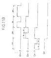
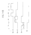
- FIG. 13A shows the configuration of a liquid crystal display according to a seventh embodiment of the present invention
- FIG. 13B shows the waveform of a driving signal applied to the scanning lines of the liquid crystal display of FIG. 13A.
- the liquid crystal display according to the seventh embodiment of the invention is constructed in such a manner that, as shown in FIG. 13A, the first and second switches are located at the right and left sides of each data line, respectively.
- the liquid crystal display of the seventh embodiment includes the plurality of scanning lines G1, G2, ..., Gn-1, Gn arranged in one direction, the plurality of data lines D1, D2, ..., Dn-1, Dn intersecting the scanning lines, the first and second switches 71 and 73 formed at both sides of each data line and controlled by a corresponding scanning line and the scanning line previous thereto, and the first and second pixel electrodes 73a and 73c respectively connected to the first and second switches 71 and 73.
- the first switch 71 includes the first thin film transistor 71a whose source or drain is connected to the data line D1 and whose gate is connected to the corresponding scanning line Gn, and the second thin film transistor 71b whose gate is connected to the previous scanning line Gn-1, the second thin film transistor being serially connected to the first thin film transistor.
- the second switches 73 includes the third thin film transistor 73a whose source or drain is connected to the data line D1 and whose gate is connected to the corresponding scanning line Gn, and the fourth thin film transistor 73b whose gate is connected to the corresponding scanning line Gn, the fourth thin film transistor 73b being serially connected to the third thin film transistor 73a.
- the second switch 73 can be configured of only the third thin film transistor 73a.
- a driving signal with the waveform of FIG. 13B is applied to the scanning lines of the liquid crystal display constructed as above, a corresponding image is displayed, moving from the lower portion to the upper portion of the liquid crystal panel. This is the same operation as that of the fifth and sixth embodiments.
- FIG. 14A shows the configuration of a liquid crystal display according to an eighth embodiment of the present invention
- FIG. 14B shows the waveform of a driving signal applied to the scanning lines of the liquid crystal display of FIG. 14A.
- the eighth embodiment of the present invention has a difference from the seventh embodiment in the connection points of the gates of the first and second thin film transistors 71a and 71b constructing the first switch 71.
- the first switch 71 according to the eighth embodiment of the invention includes the first thin film transistor 71 whose source or drain is connected to the data line D1 and whose gate is connected to the scanning line Gn-1 previous to the corresponding scanning line Gn, and a second thin film transistor 71b whose gate is connected to the corresponding scanning line Gn, the second thin film transistor 71b being connected to the first thin film transistor 71a.
- the second switch 73 has the same configuration as that of the second switch 73 according to the seventh embodiment.
- the liquid crystal display of the present invention can deliver a video signal to the pixels located at the left and right sides of each data line, resulting in reduction in the total number of the data lines by half. This also decreases the number of the source drivers each of which applies a driving signal to each data lines by half.
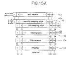
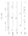
- FIG. 15A shows a source driver according to an embodiment of the present invention.
- the source driver of FIG. 15A includes a sampling latch having cells twice the number of that of the sampling latch of a conventional source driver. This is because the source driver should process image data corresponding to 784 lines though it drives the 384 data lines.
- the source driver of the present invention includes: a 128-clock shift register 151 for shifting a horizontal synchronous signal pulse depending on a source pulse clock HCLK to output a latch clock; a first sampling latch 152 for sampling and latching digital R, G, B data corresponding to odd-numbered column lines among the 768 column lines according to the latch clock sent from the shift register 151; a second sampling latch 153a for sampling and latching digital R, G, B data corresponding to even-numbered column lines among the 768 lines; a holding latch 153 for receiving and latching the data items, respectively stored in the first and second sampling latches 152 and 152, according to first and second load signals LDO and LDE, respectively; a D/A converter 154 for converting the digital R, G, B data corresponding to the odd-numbered column lines or the digital data corresponding to the even-numbered column lines, stored in the holding latch 153, into analog data signals; and an amplifier 155 for amplifying the currents of the analog R, G, and
- the source driver has the first sampling latch 152 which samples and latches the image data corresponding to the odd-numbered column lines among the 768 lines in total, and the second sampling latch 152a which samples and latches the image data corresponding to the even-numbered column lines.
- the R, G, and B data corresponding to the odd-numbered column lines is sampled and latched by the first sampling latch 152 during the first half of the horizontal period (it may not be the exact one-half), and the R, G, and B data corresponding to the even-numbered column lines is sampled and latched by the second sampling latch 152a during the second half.
- the R, G, and B data of the 768 column lines can be sampled.
- the digital video signals latched by the first and second sampling latches 152 and 152a are sequentially transmitted to the holding latch 153.
- the image data stored in the first sampling latch 152 is loaded in the holding latch 153 according to the first load signal LDO whereas the image data stored in the second sampling latch 152a is loaded into the holding latch 153 according to the second load signal LDE.
- the digital R, G, B data loaded into the holding latch 153 is converted into the analog signal by the D/A converter 154, to be amplified by the amplifier 155.
- the R, G, and B data corresponding to the odd-numbered column lines are applied to the liquid crystal panel to be displayed during the first half of the horizontal period, and the R, G, B data of the even-numbered column lines is applied to the panel to be displayed during the second half.
- FIG. 15B shows the operation waveforms of the source driver of FIG. 15A. It can be known from the FIG. 15B that the sampled odd-numbered column data and the sampled even-numbered column data are loaded into the holding latch 153 during one horizontal period.
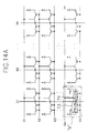
- FIG. 16A shows a source driver according to another embodiment of the present invention.
- the source driver of FIG. 16A has first and second sampling latches 162 and 162a, first and second holding latches 163 and 163a, first and second D/A converters 164 and 164a and first and second amplifiers 165 and 165a for the purpose of applying image data to the liquid crystal panel, dividing it into odd-numbered column data and even-numbered column data, during one horizontal period.
- the source driver according to the second embodiment of the invention includes a switch 166 for selectively delivering the outputs of the two amplifiers 165 and 165a to the data lines.
- the first sampling latch 162 samples image data corresponding to the odd-numbered column lines while the second latch 162a sampled image data of the even-numbered column lines.
- the image data of the odd-numbered column lines latched by the first sampling latch 162 are loaded into the first holding latch 163 according to a load signal LD.
- the image data of the even-numbered column lines latched by the second sampling latch 162a are loaded into the second holding latch 163a according to the load signal LD.
- the digital image data stored in the first holding latch 163 are converted by the first D/A converter 164 into analog signals while the image data stored in the second holding latch 163a are converted by the second D/A converter 164a into analog signals.
- the first and second D/A converters 164 and 164a convert the image data corresponding to the odd-numbered column lines and the image data of the even-numbered column lines into the analog signals, respectively.
- the converted analog video signals corresponding to the odd-numbered and even-numbered column lines are amplified by the first and second amplifiers 165 and 165a, respectively.
- the analog video signals corresponding to the odd-numbered column lines are applied to the data lines under the operation of the switch 166.
- the analog video signals corresponding to the even-numbered column lines are applied to the data lines according to the switch 166.
- the switch 166 electrically connects the outputs of the first amplifier 165 to the data lines D1, D2, ..., Dn-1, Dn during the first half of the horizontal period while it electrically connects the outputs of the second amplifier 165a to the data lines during the second half.
- the source driver consists of two sampling latches, holding latches, D/A converters and amplifiers, to thereby apply the video signals corresponding to 2n column lines using n column lines.
- FIG. 17A shows a gate driver according to a first embodiment of the present invention.
- the gate driver includes a shift register 171, a logic circuit 172, a level shifter 173 and an output buffer 174.
- the shift register 171 shifts a vertical synchronous signal pulse VSYNC depending on a gate pulse clock VCLK.
- the logic circuit 172 consists of a plurality of 3-input OR-gates OR1, OR2, ..., ORn each of which selectively receives three outputs of the shift register 171 and logically operates them.
- the first 3-input OR-gate OR1 receives outputs S1, S3 and S4 from S1 to Sn of the shift register 171, the second one receives outputs S3, S5 and S6, and the third one receives outputs S5, S7 and S8.
- Each of the fourth 3-input OR-gate to the final one also receives three outputs of the shift registers 171 in this manner.
- the level shifter 173 sequentially level-shifts a signal applied to the scanning lines to send the level-shifted signals to the output buffer 174. Accordingly, the plural scanning lines connected to the output buffer 174 are sequentially enabled.
- the operation of the gate driver according to the first embodiment of the present invention is described below with reference to FIG. 17B.
- the first scanning line G1 receives the output waveform of the first OR-gate OR1
- the second scanning line G2 receives the output waveform of the second OR-gate OR2.
- the first scanning line to the last one are sequentially enabled in this manner.
- each of the signals applied to the scanning lines G1, G2, ..., Gn-1, Gn repeats 'high' and 'low' states during one horizontal period. This is the same as the waveform of one of the driving signals shown in FIGS. 7B to 10B.
- the OR-gates shown in FIG. 17A may receive the outputs of the shift register 171 in a different manner.
- the first OR-gate receives the outputs S1 and S2
- the second OR-gate receives the outputs S1, S3 and S4, the third one receives outputs S3, S5 and S6 and so forth.
- Each of the fourth OR-gate to the last one receives three outputs of the shift register according to this rule.
- the driving signal applied to the scanning lines has waveforms G1', G2' and G3' shown in the lower portion of FIG. 17B.
- the liquid crystal display of the present invention which transmits two video signals to two pixels, respectively, during one horizontal period by the gate driver and source driver constructed as above can reduce the total number of the data lines, resulting in decrease in the number of the source drivers.
- the line time during which a video signal is delivered to each pixel is reduced because two video signals are needed to be sent to two pixels during one horizontal period.
- the video signals are written in the order indicated by numbers shown in FIG. 18. Th is precharged at the moment when is is written because both of is and an are positive signals. Thus, charging can be carried out during only one-half of one horizontal period. ar and an require longer time for charging and discharging since their polarities are opposite to those of e and an. Accordingly, during the blanking time between writing of A and an and writing of an and an, the charging and discharging time is reduced by data line precharge or charge sharing between the data lines. There is no writing time problem with because it is precharged during be is written. However, there may be a problem in writing of is. To solve this, the magnitudes of the 'high' and 'low' sections (a) and (b) of the driving signal applied to the scanning lines during one horizontal period are controlled to secure the time required for writing al.
- the liquid crystal display and driving circuit thereof has the following advantages. First of all, one data line can selectively deliver a video signal to two pixels located at the left and right sides thereof, resulting in reduction in the number of the data lines by half. This also decreases the number of the source drivers by half. Accordingly, it is possible to reduce the size of the display and the cost for manufacturing it. Moreover, more images can be displayed in the same size than in the conventional display, realizing a high resolution. It will be apparent to those skilled in the art that various modifications and variations can be made in the liquid crystal display and circuit for driving the same of the present invention without departing from the spirit or scope of the invention. Thus, it is intended that the present invention covers the modifications and variations of this invention provided they come within the scope of the appended claims and their equivalents.
Landscapes
- Engineering & Computer Science (AREA)
- Physics & Mathematics (AREA)
- General Physics & Mathematics (AREA)
- Crystallography & Structural Chemistry (AREA)
- Chemical & Material Sciences (AREA)
- Theoretical Computer Science (AREA)
- Computer Hardware Design (AREA)
- Nonlinear Science (AREA)
- Mathematical Physics (AREA)
- Optics & Photonics (AREA)
- Liquid Crystal Display Device Control (AREA)
- Liquid Crystal (AREA)
- Control Of Indicators Other Than Cathode Ray Tubes (AREA)
- Devices For Indicating Variable Information By Combining Individual Elements (AREA)
- Shift Register Type Memory (AREA)
Applications Claiming Priority (2)
| Application Number | Priority Date | Filing Date | Title |
|---|---|---|---|
| KR1019990020721A KR100291770B1 (ko) | 1999-06-04 | 1999-06-04 | 액정표시장치 |
| KR9920721 | 1999-06-04 |
Publications (3)
| Publication Number | Publication Date |
|---|---|
| EP1058232A2 true EP1058232A2 (de) | 2000-12-06 |
| EP1058232A3 EP1058232A3 (de) | 2001-04-18 |
| EP1058232B1 EP1058232B1 (de) | 2011-11-02 |
Family
ID=19590163
Family Applications (3)
| Application Number | Title | Priority Date | Filing Date |
|---|---|---|---|
| EP00112043A Expired - Lifetime EP1061498B1 (de) | 1999-06-04 | 2000-06-02 | Gate-Treiber für eine Flüssigkristallanzeige |
| EP00112044A Ceased EP1058233A3 (de) | 1999-06-04 | 2000-06-02 | Flüssigkristallanzeigegerät |
| EP00112042A Expired - Lifetime EP1058232B1 (de) | 1999-06-04 | 2000-06-02 | Flüssigkristallanzeige |
Family Applications Before (2)
| Application Number | Title | Priority Date | Filing Date |
|---|---|---|---|
| EP00112043A Expired - Lifetime EP1061498B1 (de) | 1999-06-04 | 2000-06-02 | Gate-Treiber für eine Flüssigkristallanzeige |
| EP00112044A Ceased EP1058233A3 (de) | 1999-06-04 | 2000-06-02 | Flüssigkristallanzeigegerät |
Country Status (7)
| Country | Link |
|---|---|
| US (2) | US6525710B1 (de) |
| EP (3) | EP1061498B1 (de) |
| JP (3) | JP2001027751A (de) |
| KR (1) | KR100291770B1 (de) |
| CN (3) | CN1129026C (de) |
| AT (1) | ATE532168T1 (de) |
| TW (1) | TW559765B (de) |
Cited By (12)
| Publication number | Priority date | Publication date | Assignee | Title |
|---|---|---|---|---|
| GB2380848A (en) * | 2001-10-13 | 2003-04-16 | Lg Philips Lcd Co Ltd | Data driving apparatus and method for liquid crystal display |
| GB2380849A (en) * | 2001-10-13 | 2003-04-16 | Lg Philips Lcd Co Ltd | Data driving apparatus and method for liquid crystal display |
| GB2381645A (en) * | 2001-11-03 | 2003-05-07 | Lg Philips Lcd Co Ltd | Data driving apparatus and method for liquid crystal display |
| NL1022335C2 (nl) * | 2003-01-09 | 2004-07-13 | Lg Philips Lcd Co | Gegevensbesturingstoestel en werkwijze voor vloeibaar-kristalbeeldscherm. |
| NL1022334C2 (nl) * | 2003-01-09 | 2004-07-13 | Lg Philips Lcd Co | Gegevensbesturingstoestel en werkwijze voor vloeibaar-kristalscherm. |
| NL1022336C2 (nl) * | 2003-01-09 | 2004-07-13 | Lg Philips Lcd Co | Gegevensbesturingstoestel en werkwijze voor vloeibaar-kristalbeeldscherm. |
| US6933914B2 (en) | 2001-07-24 | 2005-08-23 | International Business Machines Corporation | Image display apparatus |
| EP1492078A3 (de) * | 2003-06-23 | 2006-05-17 | Samsung Electronics Co., Ltd. | Anzeigesteuervorrichtung mit unterteilter Gatetreibereinheit und Flüssigkristallanzeigegerät und Verfahren mit Verwendung dieser Anzeigesteuervorrichtung |
| CN100383618C (zh) * | 2004-05-31 | 2008-04-23 | Lg.菲利浦Lcd株式会社 | 具有内置驱动电路的液晶显示板 |
| CN100410996C (zh) * | 2003-03-26 | 2008-08-13 | 恩益禧电子股份有限公司 | 具有两个不同交错象素的保持型图像显示装置及驱动方法 |
| CN101110187B (zh) * | 2006-07-20 | 2010-07-21 | 晶门科技有限公司 | 在显示系统中提高列线输出的均匀性的驱动电路、系统以及方法 |
| US10281788B2 (en) | 2007-05-17 | 2019-05-07 | Semiconductor Energy Laboratory Co., Ltd. | Liquid crystal display device |
Families Citing this family (97)
| Publication number | Priority date | Publication date | Assignee | Title |
|---|---|---|---|---|
| KR100848099B1 (ko) | 2002-05-27 | 2008-07-24 | 삼성전자주식회사 | 액정 표시 장치용 박막 트랜지스터 기판 |
| TW525127B (en) * | 2000-05-29 | 2003-03-21 | Hannstar Display Corp | Point inversion active matrix type liquid crystal display having pre-write circuit |
| KR100741903B1 (ko) * | 2000-10-23 | 2007-07-24 | 엘지.필립스 엘시디 주식회사 | 액정 적하 방식의 lcd 패널 및 그 제조방법 |
| US6747626B2 (en) * | 2000-11-30 | 2004-06-08 | Texas Instruments Incorporated | Dual mode thin film transistor liquid crystal display source driver circuit |
| JP2002175036A (ja) * | 2000-12-07 | 2002-06-21 | Sanyo Electric Co Ltd | アクティブマトリクス型表示装置 |
| JP4540219B2 (ja) * | 2000-12-07 | 2010-09-08 | エーユー オプトロニクス コーポレイション | 画像表示素子、画像表示装置、画像表示素子の駆動方法 |
| KR100367014B1 (ko) * | 2000-12-29 | 2003-01-09 | 엘지.필립스 엘시디 주식회사 | 액정 표시장치 및 그 구동방법 |
| TW525139B (en) * | 2001-02-13 | 2003-03-21 | Samsung Electronics Co Ltd | Shift register, liquid crystal display using the same and method for driving gate line and data line blocks thereof |
| JP3579368B2 (ja) * | 2001-05-09 | 2004-10-20 | 三洋電機株式会社 | 駆動回路および表示装置 |
| JP4647843B2 (ja) * | 2001-06-28 | 2011-03-09 | 株式会社日立製作所 | 液晶表示装置 |
| US7006072B2 (en) | 2001-11-10 | 2006-02-28 | Lg.Philips Lcd Co., Ltd. | Apparatus and method for data-driving liquid crystal display |
| JPWO2003060868A1 (ja) | 2002-01-17 | 2005-05-19 | インターナショナル・ビジネス・マシーンズ・コーポレーションInternational Business Maschines Corporation | 表示装置、走査線用ドライバ回路 |
| JP4117134B2 (ja) * | 2002-02-01 | 2008-07-16 | シャープ株式会社 | 液晶表示装置 |
| JP3872377B2 (ja) * | 2002-04-30 | 2007-01-24 | インターナショナル・ビジネス・マシーンズ・コーポレーション | 画像表示素子および画像表示装置 |
| KR100853773B1 (ko) * | 2002-05-28 | 2008-08-25 | 엘지디스플레이 주식회사 | 액정패널의 구동방법 |
| JP4090799B2 (ja) * | 2002-07-01 | 2008-05-28 | 奇美電子股▲ふん▼有限公司 | 画像表示素子及び画像表示装置 |
| KR100909047B1 (ko) * | 2002-10-19 | 2009-07-23 | 엘지디스플레이 주식회사 | 액정표시장치 |
| KR100909048B1 (ko) * | 2002-10-24 | 2009-07-23 | 엘지디스플레이 주식회사 | 액정표시장치 및 그 구동방법 |
| KR100942836B1 (ko) * | 2002-12-20 | 2010-02-18 | 엘지디스플레이 주식회사 | 액정표시장치의 구동장치 및 방법 |
| KR100923350B1 (ko) * | 2002-12-20 | 2009-10-22 | 엘지디스플레이 주식회사 | 액정표시장치 및 그의 구동방법 |
| KR100898791B1 (ko) | 2002-12-21 | 2009-05-20 | 엘지디스플레이 주식회사 | 액정표시장치의 구동장치 및 방법 |
| KR100961945B1 (ko) * | 2003-03-26 | 2010-06-08 | 삼성전자주식회사 | 액정 표시 장치 및 그에 사용되는 표시판 |
| WO2004090622A1 (fr) * | 2003-04-11 | 2004-10-21 | Quanta Display Inc. | Afficheur a cristaux liquides comportant une structure de pixels a transistors a film mince double |
| KR100913303B1 (ko) * | 2003-05-06 | 2009-08-26 | 삼성전자주식회사 | 액정표시장치 |
| CN1315330C (zh) * | 2003-05-12 | 2007-05-09 | 瑞昱半导体股份有限公司 | 视频信号处理方法及其装置 |
| CN100363971C (zh) * | 2003-06-03 | 2008-01-23 | 友达光电股份有限公司 | 数字型数据驱动器及液晶显示器 |
| KR100933446B1 (ko) * | 2003-06-20 | 2009-12-23 | 엘지디스플레이 주식회사 | 액정표시장치의 구동장치 및 구동방법 |
| KR100922794B1 (ko) * | 2003-06-24 | 2009-10-21 | 엘지디스플레이 주식회사 | 액정표시장치 |
| KR100933448B1 (ko) * | 2003-06-24 | 2009-12-23 | 엘지디스플레이 주식회사 | 액정표시장치의 구동장치 및 구동방법 |
| KR100552905B1 (ko) | 2003-06-30 | 2006-02-22 | 엘지.필립스 엘시디 주식회사 | 액정표시장치의 구동장치 및 구동방법 |
| KR100541534B1 (ko) * | 2003-06-30 | 2006-01-11 | 엘지.필립스 엘시디 주식회사 | 액정표시장치용 어레이기판과 그 제조방법 |
| JP3726910B2 (ja) * | 2003-07-18 | 2005-12-14 | セイコーエプソン株式会社 | 表示ドライバ及び電気光学装置 |
| US7173600B2 (en) | 2003-10-15 | 2007-02-06 | International Business Machines Corporation | Image display device, pixel drive method, and scan line drive circuit |
| KR100963403B1 (ko) * | 2003-12-08 | 2010-06-14 | 엘지디스플레이 주식회사 | 액정표시장치 및 그의 구동방법 |
| JP4168339B2 (ja) * | 2003-12-26 | 2008-10-22 | カシオ計算機株式会社 | 表示駆動装置及びその駆動制御方法並びに表示装置 |
| FR2866465A1 (fr) * | 2004-02-18 | 2005-08-19 | Thomson Licensing Sa | Dispositif d'affichage avec valve lcos de taille reduite |
| JP2005300885A (ja) * | 2004-04-12 | 2005-10-27 | Koninkl Philips Electronics Nv | 液晶表示装置 |
| KR101090248B1 (ko) * | 2004-05-06 | 2011-12-06 | 삼성전자주식회사 | 칼럼 드라이버 및 이를 갖는 평판 표시 장치 |
| KR101028947B1 (ko) * | 2004-05-31 | 2011-04-12 | 엘지디스플레이 주식회사 | 쉬프트 레지스터 회로 |
| CN100392483C (zh) * | 2004-07-30 | 2008-06-04 | 精工爱普生株式会社 | 电光装置用驱动电路、电光装置及电子设备 |
| KR101061854B1 (ko) * | 2004-10-01 | 2011-09-02 | 삼성전자주식회사 | 액정 표시 장치 및 그 구동 방법 |
| KR100595099B1 (ko) * | 2004-11-08 | 2006-06-30 | 삼성에스디아이 주식회사 | 데이터 집적회로와 이를 이용한 발광 표시장치 및 그의구동방법 |
| CN1779770B (zh) * | 2004-11-19 | 2010-10-13 | 中华映管股份有限公司 | 平面显示器与栅极驱动方法 |
| JP2006267999A (ja) * | 2005-02-28 | 2006-10-05 | Nec Electronics Corp | 駆動回路チップ及び表示装置 |
| KR101209289B1 (ko) * | 2005-04-07 | 2012-12-10 | 삼성디스플레이 주식회사 | 표시 패널과, 이를 구비한 표시 장치 및 구동 방법 |
| CN101958095B (zh) * | 2005-04-26 | 2012-10-03 | 株式会社半导体能源研究所 | 发光装置及其驱动方法 |
| KR100665943B1 (ko) * | 2005-06-30 | 2007-01-09 | 엘지.필립스 엘시디 주식회사 | 유기전계 발광 디스플레이 장치 및 구동방법 |
| KR101230303B1 (ko) * | 2005-08-29 | 2013-02-06 | 삼성디스플레이 주식회사 | 접촉 감지 기능이 있는 표시 장치 |
| KR100662988B1 (ko) * | 2005-10-31 | 2006-12-28 | 삼성에스디아이 주식회사 | 데이터 구동회로와 이를 이용한 발광 표시장치 및 그의구동방법 |
| KR100732809B1 (ko) * | 2005-11-03 | 2007-06-27 | 삼성에스디아이 주식회사 | 데이터 구동부 및 이를 이용한 유기 발광표시장치 |
| TWI345213B (en) * | 2006-03-09 | 2011-07-11 | Au Optronics Corp | Low color-shift liquid crystal display and its driving method |
| TWI326068B (en) | 2006-03-31 | 2010-06-11 | Au Optronics Corp | Pixel drive method and flat panel display |
| KR100719670B1 (ko) * | 2006-04-06 | 2007-05-18 | 삼성에스디아이 주식회사 | 데이터 구동부 및 이를 이용한 유기 전계발광 표시장치 |
| CN100414365C (zh) * | 2006-04-25 | 2008-08-27 | 友达光电股份有限公司 | 扫描驱动方法及其平面显示器 |
| CN100388071C (zh) * | 2006-04-26 | 2008-05-14 | 友达光电股份有限公司 | 液晶显示面板的驱动方法 |
| CN100426372C (zh) * | 2006-06-14 | 2008-10-15 | 友达光电股份有限公司 | 数据驱动电路、液晶显示面板、液晶显示模块以及显示器 |
| KR101286506B1 (ko) * | 2006-06-19 | 2013-07-16 | 엘지디스플레이 주식회사 | 액정 표시장치와 그의 구동방법 |
| KR100801416B1 (ko) * | 2006-06-21 | 2008-02-11 | 한양대학교 산학협력단 | 액정표시장치의 게이트 라인 및 데이터 라인 공유 회로 및이의 구동방법 |
| KR101252854B1 (ko) * | 2006-06-29 | 2013-04-09 | 엘지디스플레이 주식회사 | 액정 패널, 데이터 드라이버, 이를 구비한 액정표시장치 및그 구동 방법 |
| TW200811796A (en) * | 2006-08-22 | 2008-03-01 | Quanta Display Inc | Display method for improving PLM image quality and device used the same |
| TWI330746B (en) * | 2006-08-25 | 2010-09-21 | Au Optronics Corp | Liquid crystal display and operation method thereof |
| KR101429905B1 (ko) * | 2006-09-29 | 2014-08-14 | 엘지디스플레이 주식회사 | 액정표시장치 |
| TWI341505B (en) * | 2006-11-27 | 2011-05-01 | Chimei Innolux Corp | Liquid crystal panel and driving method thereof |
| CN101191922B (zh) * | 2006-12-01 | 2010-04-14 | 群康科技(深圳)有限公司 | 液晶显示面板 |
| US7920668B2 (en) * | 2007-01-05 | 2011-04-05 | Chimei Innolux Corporation | Systems for displaying images by utilizing vertical shift register circuit to generate non-overlapped output signals |
| TW200830247A (en) * | 2007-01-09 | 2008-07-16 | Denmos Technology Inc | Gate driver |
| TWI326789B (en) * | 2007-02-15 | 2010-07-01 | Au Optronics Corp | Active device array substrate and driving method thereof |
| TWI366174B (en) * | 2007-03-03 | 2012-06-11 | Au Optronics Corp | Pixel control device and display apparatus utilizing said pixel control device |
| JP4270310B2 (ja) | 2007-03-29 | 2009-05-27 | カシオ計算機株式会社 | アクティブマトリックス型表示装置の駆動回路、駆動方法及びアクティブマトリックス型表示装置 |
| KR101385467B1 (ko) * | 2007-06-01 | 2014-04-17 | 엘지디스플레이 주식회사 | 액정표시장치 |
| KR101492885B1 (ko) | 2007-08-10 | 2015-02-12 | 삼성전자주식회사 | 구동회로 및 이를 포함하는 액정 표시 장치 |
| US20090046044A1 (en) * | 2007-08-14 | 2009-02-19 | Himax Technologies Limited | Apparatus for driving a display panel |
| JP5211585B2 (ja) * | 2007-08-30 | 2013-06-12 | カシオ計算機株式会社 | アクティブマトリックス型表示装置 |
| US7598894B2 (en) * | 2007-10-19 | 2009-10-06 | Himax Technologies Limited | Source driver and digital-to-analog converter thereof |
| KR101563692B1 (ko) * | 2007-10-19 | 2015-10-27 | 가부시키가이샤 한도오따이 에네루기 켄큐쇼 | 표시장치 및 그 구동 방법 |
| JP4483945B2 (ja) | 2007-12-27 | 2010-06-16 | ソニー株式会社 | 表示装置及び電子機器 |
| TWI375061B (en) * | 2008-05-30 | 2012-10-21 | Chimei Innolux Corp | Liquid crystal display panel |
| JP4775407B2 (ja) * | 2008-05-30 | 2011-09-21 | カシオ計算機株式会社 | 表示装置 |
| JP2010049041A (ja) * | 2008-08-22 | 2010-03-04 | Sony Corp | 画像表示装置及び画像表示装置の駆動方法 |
| JP5211972B2 (ja) * | 2008-09-17 | 2013-06-12 | カシオ計算機株式会社 | 表示装置及び表示装置の駆動方法 |
| TWI369563B (en) * | 2008-11-06 | 2012-08-01 | Au Optronics Corp | Pixel circuit and driving method thereof |
| JP5273391B2 (ja) * | 2009-12-21 | 2013-08-28 | 株式会社ジャパンディスプレイ | 液晶表示装置 |
| KR101094291B1 (ko) | 2010-04-09 | 2011-12-20 | 삼성모바일디스플레이주식회사 | 액정 표시 장치 |
| JP2010224564A (ja) * | 2010-05-20 | 2010-10-07 | Casio Computer Co Ltd | 表示装置 |
| JP5370264B2 (ja) * | 2010-05-20 | 2013-12-18 | カシオ計算機株式会社 | 表示装置 |
| WO2013172243A1 (ja) * | 2012-05-16 | 2013-11-21 | シャープ株式会社 | 液晶ディスプレイ |
| TWI502579B (zh) * | 2013-12-11 | 2015-10-01 | Au Optronics Corp | 顯示面板 |
| KR20150078310A (ko) * | 2013-12-30 | 2015-07-08 | 삼성디스플레이 주식회사 | 표시 장치 |
| CN104298041B (zh) * | 2014-11-10 | 2017-04-26 | 深圳市华星光电技术有限公司 | 阵列基板、液晶面板以及液晶显示器 |
| CN104474148A (zh) * | 2015-01-16 | 2015-04-01 | 杜卫兵 | 用于治疗真菌性皮肤病的中药组合物及其制备方法 |
| CN105185325A (zh) | 2015-08-12 | 2015-12-23 | 深圳市华星光电技术有限公司 | 一种液晶显示驱动系统及驱动方法 |
| DE112016006644B4 (de) * | 2016-03-23 | 2021-11-04 | Mitsubishi Electric Corporation | Heizvorrichtung vom wärmepumpentyp |
| CN106501984B (zh) * | 2016-12-28 | 2019-12-13 | 武汉华星光电技术有限公司 | 内嵌式触控液晶显示面板及制作方法 |
| JP6359732B2 (ja) * | 2017-07-06 | 2018-07-18 | 株式会社半導体エネルギー研究所 | 液晶表示装置 |
| KR102513173B1 (ko) * | 2017-11-15 | 2023-03-24 | 삼성전자주식회사 | 픽셀 그룹별 독립적 제어가 가능한 디스플레이 장치 및 방법 |
| KR102392336B1 (ko) * | 2017-11-15 | 2022-04-28 | 삼성전자주식회사 | 디스플레이 구동 장치 및 이를 포함하는 디스플레이 시스템 |
| CN113728375B (zh) * | 2020-02-20 | 2023-01-24 | 京东方科技集团股份有限公司 | 显示面板、其驱动方法及显示装置 |
Family Cites Families (29)
| Publication number | Priority date | Publication date | Assignee | Title |
|---|---|---|---|---|
| JPS59225683A (ja) * | 1983-06-07 | 1984-12-18 | Seiko Epson Corp | テレビ用デイスプレイの駆動方法 |
| US4822142A (en) * | 1986-12-23 | 1989-04-18 | Hosiden Electronics Co. Ltd. | Planar display device |
| GB2205191A (en) * | 1987-05-29 | 1988-11-30 | Philips Electronic Associated | Active matrix display system |
| JPS6437585A (en) * | 1987-08-04 | 1989-02-08 | Nippon Telegraph & Telephone | Active matrix type display device |
| US5151689A (en) * | 1988-04-25 | 1992-09-29 | Hitachi, Ltd. | Display device with matrix-arranged pixels having reduced number of vertical signal lines |
| JPH0287190A (ja) * | 1988-09-22 | 1990-03-28 | Toshiba Corp | フルライン駆動方式のディスプレイ装置 |
| EP0368572B1 (de) * | 1988-11-05 | 1995-08-02 | SHARP Corporation | Steuereinrichtung und -verfahren für eine Flüssigkristallanzeigetafel |
| KR950001360B1 (ko) * | 1990-11-26 | 1995-02-17 | 가부시키가이샤 한도오따이 에네루기 겐큐쇼 | 전기 광학장치와 그 구동방법 |
| KR960010723B1 (ko) * | 1990-12-20 | 1996-08-07 | 가부시끼가이샤 한도오따이 에네루기 겐큐쇼 | 전기광학장치 |
| JPH0535200A (ja) * | 1991-07-31 | 1993-02-12 | Hitachi Ltd | 表示装置とその駆動方法 |
| JPH05188395A (ja) * | 1992-01-14 | 1993-07-30 | Toshiba Corp | 液晶表示素子 |
| JP3091300B2 (ja) * | 1992-03-19 | 2000-09-25 | 富士通株式会社 | アクティブマトリクス型液晶表示装置及びその駆動回路 |
| JPH05303114A (ja) * | 1992-04-27 | 1993-11-16 | Toshiba Corp | 液晶表示素子 |
| US5313222A (en) * | 1992-12-24 | 1994-05-17 | Yuen Foong Yu H. K. Co., Ltd. | Select driver circuit for an LCD display |
| KR950007126B1 (ko) * | 1993-05-07 | 1995-06-30 | 삼성전자주식회사 | 액정 디스플레이 구동장치 |
| JP2671772B2 (ja) * | 1993-09-06 | 1997-10-29 | 日本電気株式会社 | 液晶ディスプレイとその駆動方法 |
| JP3438190B2 (ja) * | 1994-03-14 | 2003-08-18 | 株式会社日立製作所 | Tftディスプレイ装置 |
| JP3219640B2 (ja) * | 1994-06-06 | 2001-10-15 | キヤノン株式会社 | ディスプレイ装置 |
| US5528256A (en) * | 1994-08-16 | 1996-06-18 | Vivid Semiconductor, Inc. | Power-saving circuit and method for driving liquid crystal display |
| JP3184069B2 (ja) * | 1994-09-02 | 2001-07-09 | シャープ株式会社 | 画像表示装置 |
| US5883609A (en) * | 1994-10-27 | 1999-03-16 | Nec Corporation | Active matrix type liquid crystal display with multi-media oriented drivers and driving method for same |
| JPH08234703A (ja) * | 1995-02-28 | 1996-09-13 | Sony Corp | 表示装置 |
| KR0161918B1 (ko) * | 1995-07-04 | 1999-03-20 | 구자홍 | 액정표시장치의 데이타 드라이버 |
| JPH09281931A (ja) * | 1996-04-10 | 1997-10-31 | Fujitsu Ltd | 表示装置および該表示装置の駆動回路ならびに表示装置の駆動方法 |
| KR100214484B1 (ko) * | 1996-06-07 | 1999-08-02 | 구본준 | 순차 및 이중스캐닝방식을 위한 티에프티-엘씨디구동회로 |
| JPH10177370A (ja) * | 1996-10-16 | 1998-06-30 | Oki Lsi Technol Kansai:Kk | 多階調出力回路及び液晶表示装置 |
| KR100236333B1 (ko) * | 1997-03-05 | 1999-12-15 | 구본준, 론 위라하디락사 | 액정표시장치의 데이터 구동 장치 및 구동 방법 |
| JP3516840B2 (ja) * | 1997-07-24 | 2004-04-05 | アルプス電気株式会社 | 表示装置およびその駆動方法 |
| JPH11126051A (ja) * | 1997-10-24 | 1999-05-11 | Canon Inc | マトリクス基板と液晶表示装置及びこれを用いる投写型液晶表示装置 |
-
1999
- 1999-06-04 KR KR1019990020721A patent/KR100291770B1/ko not_active IP Right Cessation
-
2000
- 2000-06-02 US US09/587,145 patent/US6525710B1/en not_active Expired - Lifetime
- 2000-06-02 EP EP00112043A patent/EP1061498B1/de not_active Expired - Lifetime
- 2000-06-02 EP EP00112044A patent/EP1058233A3/de not_active Ceased
- 2000-06-02 AT AT00112042T patent/ATE532168T1/de active
- 2000-06-02 EP EP00112042A patent/EP1058232B1/de not_active Expired - Lifetime
- 2000-06-02 US US09/585,760 patent/US6486930B1/en not_active Expired - Lifetime
- 2000-06-03 TW TW089110913A patent/TW559765B/zh not_active IP Right Cessation
- 2000-06-04 CN CN00126436A patent/CN1129026C/zh not_active Expired - Lifetime
- 2000-06-04 CN CNB001200216A patent/CN1154000C/zh not_active Expired - Lifetime
- 2000-06-04 CN CNB001201654A patent/CN1139909C/zh not_active Expired - Lifetime
- 2000-06-05 JP JP2000167912A patent/JP2001027751A/ja active Pending
- 2000-06-05 JP JP2000167947A patent/JP2001042842A/ja active Pending
- 2000-06-05 JP JP2000167959A patent/JP2001027893A/ja active Pending
Non-Patent Citations (1)
| Title |
|---|
| None |
Cited By (28)
| Publication number | Priority date | Publication date | Assignee | Title |
|---|---|---|---|---|
| US6933914B2 (en) | 2001-07-24 | 2005-08-23 | International Business Machines Corporation | Image display apparatus |
| US7180499B2 (en) | 2001-10-13 | 2007-02-20 | Lg. Philips Lcd Co., Ltd. | Data driving apparatus and method for liquid crystal display |
| GB2380849A (en) * | 2001-10-13 | 2003-04-16 | Lg Philips Lcd Co Ltd | Data driving apparatus and method for liquid crystal display |
| US7916110B2 (en) | 2001-10-13 | 2011-03-29 | Lg Display Co., Ltd. | Data driving apparatus and method for liquid crystal display |
| FR2830968A1 (fr) * | 2001-10-13 | 2003-04-18 | Lg Philips Lcd Co Ltd | Dispositif et procede de commande de donnees dans un afficheur a cristaux liquides |
| GB2380848A (en) * | 2001-10-13 | 2003-04-16 | Lg Philips Lcd Co Ltd | Data driving apparatus and method for liquid crystal display |
| GB2380849B (en) * | 2001-10-13 | 2003-11-26 | Lg Philips Lcd Co Ltd | Data driving apparatus and method for liquid crystal display |
| GB2380848B (en) * | 2001-10-13 | 2003-11-26 | Lg Philips Lcd Co Ltd | Data driving apparatus and method for liquid crystal display |
| FR2830969A1 (fr) * | 2001-10-13 | 2003-04-18 | Lg Philips Lcd Co Ltd | Dispositif de pilotage de donnees et procede d'utilisation pour un panneau d'affichage a cristaux liquides |
| US7196685B2 (en) | 2001-10-13 | 2007-03-27 | Lg.Philips Lcd Co., Ltd | Data driving apparatus and method for liquid crystal display |
| GB2381645B (en) * | 2001-11-03 | 2003-12-24 | Lg Philips Lcd Co Ltd | Data driving apparatus and method for liquid crystal display |
| FR2831983A1 (fr) * | 2001-11-03 | 2003-05-09 | Lg Philips Lcd Co Ltd | Afficheur a cristaux liquides et, plus particulierement, dispositif et procede de commande de donnees pour un afficheur a cristaux liquides |
| US7382344B2 (en) | 2001-11-03 | 2008-06-03 | Lg.Philips Lcd Co., Ltd. | Data driving apparatus and method for liquid crystal display |
| GB2381645A (en) * | 2001-11-03 | 2003-05-07 | Lg Philips Lcd Co Ltd | Data driving apparatus and method for liquid crystal display |
| NL1022334C2 (nl) * | 2003-01-09 | 2004-07-13 | Lg Philips Lcd Co | Gegevensbesturingstoestel en werkwijze voor vloeibaar-kristalscherm. |
| NL1022336C2 (nl) * | 2003-01-09 | 2004-07-13 | Lg Philips Lcd Co | Gegevensbesturingstoestel en werkwijze voor vloeibaar-kristalbeeldscherm. |
| NL1022335C2 (nl) * | 2003-01-09 | 2004-07-13 | Lg Philips Lcd Co | Gegevensbesturingstoestel en werkwijze voor vloeibaar-kristalbeeldscherm. |
| CN100410996C (zh) * | 2003-03-26 | 2008-08-13 | 恩益禧电子股份有限公司 | 具有两个不同交错象素的保持型图像显示装置及驱动方法 |
| US8274460B2 (en) | 2003-06-23 | 2012-09-25 | Samsung Electronics Co., Ltd. | Display driving device and method and liquid crystal display apparatus having the same |
| US7385576B2 (en) | 2003-06-23 | 2008-06-10 | Samsung Electronics Co., Ltd. | Display driving device and method and liquid crystal display apparatus having the same |
| EP1492078A3 (de) * | 2003-06-23 | 2006-05-17 | Samsung Electronics Co., Ltd. | Anzeigesteuervorrichtung mit unterteilter Gatetreibereinheit und Flüssigkristallanzeigegerät und Verfahren mit Verwendung dieser Anzeigesteuervorrichtung |
| CN100383618C (zh) * | 2004-05-31 | 2008-04-23 | Lg.菲利浦Lcd株式会社 | 具有内置驱动电路的液晶显示板 |
| CN101110187B (zh) * | 2006-07-20 | 2010-07-21 | 晶门科技有限公司 | 在显示系统中提高列线输出的均匀性的驱动电路、系统以及方法 |
| US10281788B2 (en) | 2007-05-17 | 2019-05-07 | Semiconductor Energy Laboratory Co., Ltd. | Liquid crystal display device |
| US10948794B2 (en) | 2007-05-17 | 2021-03-16 | Semiconductor Energy Laboratory Co., Ltd. | Liquid crystal display device |
| US10989974B2 (en) | 2007-05-17 | 2021-04-27 | Semiconductor Energy Laboratory Co., Ltd. | Liquid crystal display device |
| US11493816B2 (en) | 2007-05-17 | 2022-11-08 | Semiconductor Energy Laboratory Co., Ltd. | Liquid crystal display device |
| US11803092B2 (en) | 2007-05-17 | 2023-10-31 | Semiconductor Energy Laboratory Co., Ltd. | Liquid crystal display device |
Also Published As
| Publication number | Publication date |
|---|---|
| EP1061498A3 (de) | 2001-02-21 |
| EP1058232B1 (de) | 2011-11-02 |
| EP1058232A3 (de) | 2001-04-18 |
| CN1281155A (zh) | 2001-01-24 |
| KR20010001483A (ko) | 2001-01-05 |
| EP1061498A2 (de) | 2000-12-20 |
| US6486930B1 (en) | 2002-11-26 |
| EP1058233A2 (de) | 2000-12-06 |
| CN1154000C (zh) | 2004-06-16 |
| CN1276590A (zh) | 2000-12-13 |
| US6525710B1 (en) | 2003-02-25 |
| JP2001027893A (ja) | 2001-01-30 |
| CN1139909C (zh) | 2004-02-25 |
| ATE532168T1 (de) | 2011-11-15 |
| KR100291770B1 (ko) | 2001-05-15 |
| EP1061498B1 (de) | 2012-10-10 |
| EP1058233A3 (de) | 2001-04-18 |
| CN1278073A (zh) | 2000-12-27 |
| TW559765B (en) | 2003-11-01 |
| JP2001042842A (ja) | 2001-02-16 |
| JP2001027751A (ja) | 2001-01-30 |
| CN1129026C (zh) | 2003-11-26 |
Similar Documents
| Publication | Publication Date | Title |
|---|---|---|
| EP1061498B1 (de) | Gate-Treiber für eine Flüssigkristallanzeige | |
| EP0275140B1 (de) | Verfahren und Schaltung zum Abtasten von kapazitiven Belastungen | |
| KR101388588B1 (ko) | 액정표시장치 | |
| KR100378101B1 (ko) | 액정 드라이버 회로 및 고속 데이타 기입 능력을 갖는lcd | |
| JP3638121B2 (ja) | データ信号線駆動回路およびそれを備える画像表示装置 | |
| EP2610852B1 (de) | Flüssigkristallanzeigevorrichtung, Antriebsvorrichtung für Flüssigkristallanzeigetafel und Flüssigkristallanzeigetafel | |
| KR101393628B1 (ko) | 액정 표시 장치 | |
| EP1074966A1 (de) | Einrichtung und Verfahren zur Steuerung von Daten-Leitungen in einer Flüssigkristallanzeige | |
| US7268764B2 (en) | Liquid crystal display and driving method thereof | |
| US20060274028A1 (en) | Display drive device, display device having the same and method for driving display panel | |
| US7352314B2 (en) | Digital-to-analog converter circuit | |
| JP2008116556A (ja) | 液晶表示装置の駆動方法およびそのデータ側駆動回路 | |
| KR100549983B1 (ko) | 액정표시장치 및 그 구동방법 | |
| KR20080057501A (ko) | 액정표시장치 및 이의 구동방법 | |
| KR20060080778A (ko) | 표시장치의 구동방법 및 이를 수행하기 위한 표시장치 | |
| US8736531B2 (en) | Driving device for liquid crystal display panel | |
| KR100291768B1 (ko) | 액정표시장치의 소오스 드라이버 | |
| US7675499B2 (en) | Display device | |
| KR100291769B1 (ko) | 액정표시장치의 게이트 드라이버 | |
| KR100764047B1 (ko) | 액정 디스플레이 장치 및 그 구동방법 | |
| KR20010036307A (ko) | 플리커링을 줄이기 위한 액정 표시 장치 및 이의 구동 방법 | |
| JPH02141725A (ja) | アクティブマトリクス方式液晶表示装置 | |
| KR100363329B1 (ko) | 소스 드라이브 아이씨의 개수가 감소된 액정 디스플레이모듈 및 소스 라인들을 구동하는 방법 | |
| KR101238006B1 (ko) | 컬럼-게이트 구동부를 구비한 액정 표시장치 | |
| JPH11133934A (ja) | 液晶駆動装置及び液晶駆動方法 |
Legal Events
| Date | Code | Title | Description |
|---|---|---|---|
| PUAI | Public reference made under article 153(3) epc to a published international application that has entered the european phase |
Free format text: ORIGINAL CODE: 0009012 |
|
| AK | Designated contracting states |
Kind code of ref document: A2 Designated state(s): AT BE CH CY DE DK ES FI FR GB GR IE IT LI LU MC NL PT SE |
|
| AX | Request for extension of the european patent |
Free format text: AL;LT;LV;MK;RO;SI |
|
| PUAL | Search report despatched |
Free format text: ORIGINAL CODE: 0009013 |
|
| AK | Designated contracting states |
Kind code of ref document: A3 Designated state(s): AT BE CH CY DE DK ES FI FR GB GR IE IT LI LU MC NL PT SE |
|
| AX | Request for extension of the european patent |
Free format text: AL;LT;LV;MK;RO;SI |
|
| 17P | Request for examination filed |
Effective date: 20011016 |
|
| AKX | Designation fees paid |
Free format text: AT BE CH CY DE DK ES FI FR GB GR IE IT LI LU MC NL PT SE |
|
| RAP1 | Party data changed (applicant data changed or rights of an application transferred) |
Owner name: NEO TEK RESEARCH CO., LTD. |
|
| RIN1 | Information on inventor provided before grant (corrected) |
Inventor name: KWON, OH-KYONG |
|
| RAP1 | Party data changed (applicant data changed or rights of an application transferred) |
Owner name: SAMSUNG ELECTRONICS CO., LTD. |
|
| 17Q | First examination report despatched |
Effective date: 20080102 |
|
| RTI1 | Title (correction) |
Free format text: LIQUID CRYSTAL DISPLAY |
|
| GRAP | Despatch of communication of intention to grant a patent |
Free format text: ORIGINAL CODE: EPIDOSNIGR1 |
|
| GRAS | Grant fee paid |
Free format text: ORIGINAL CODE: EPIDOSNIGR3 |
|
| GRAA | (expected) grant |
Free format text: ORIGINAL CODE: 0009210 |
|
| AK | Designated contracting states |
Kind code of ref document: B1 Designated state(s): AT BE CH CY DE DK ES FI FR GB GR IE IT LI LU MC NL PT SE |
|
| REG | Reference to a national code |
Ref country code: GB Ref legal event code: FG4D |
|
| REG | Reference to a national code |
Ref country code: CH Ref legal event code: EP |
|
| REG | Reference to a national code |
Ref country code: IE Ref legal event code: FG4D |
|
| REG | Reference to a national code |
Ref country code: DE Ref legal event code: R096 Ref document number: 60046616 Country of ref document: DE Effective date: 20120112 |
|
| REG | Reference to a national code |
Ref country code: NL Ref legal event code: VDEP Effective date: 20111102 |
|
| PG25 | Lapsed in a contracting state [announced via postgrant information from national office to epo] |
Ref country code: NL Free format text: LAPSE BECAUSE OF FAILURE TO SUBMIT A TRANSLATION OF THE DESCRIPTION OR TO PAY THE FEE WITHIN THE PRESCRIBED TIME-LIMIT Effective date: 20111102 Ref country code: BE Free format text: LAPSE BECAUSE OF FAILURE TO SUBMIT A TRANSLATION OF THE DESCRIPTION OR TO PAY THE FEE WITHIN THE PRESCRIBED TIME-LIMIT Effective date: 20111102 Ref country code: SE Free format text: LAPSE BECAUSE OF FAILURE TO SUBMIT A TRANSLATION OF THE DESCRIPTION OR TO PAY THE FEE WITHIN THE PRESCRIBED TIME-LIMIT Effective date: 20111102 Ref country code: GR Free format text: LAPSE BECAUSE OF FAILURE TO SUBMIT A TRANSLATION OF THE DESCRIPTION OR TO PAY THE FEE WITHIN THE PRESCRIBED TIME-LIMIT Effective date: 20120203 Ref country code: PT Free format text: LAPSE BECAUSE OF FAILURE TO SUBMIT A TRANSLATION OF THE DESCRIPTION OR TO PAY THE FEE WITHIN THE PRESCRIBED TIME-LIMIT Effective date: 20120302 |
|
| PG25 | Lapsed in a contracting state [announced via postgrant information from national office to epo] |
Ref country code: CY Free format text: LAPSE BECAUSE OF FAILURE TO SUBMIT A TRANSLATION OF THE DESCRIPTION OR TO PAY THE FEE WITHIN THE PRESCRIBED TIME-LIMIT Effective date: 20111102 |
|
| PG25 | Lapsed in a contracting state [announced via postgrant information from national office to epo] |
Ref country code: DK Free format text: LAPSE BECAUSE OF FAILURE TO SUBMIT A TRANSLATION OF THE DESCRIPTION OR TO PAY THE FEE WITHIN THE PRESCRIBED TIME-LIMIT Effective date: 20111102 |
|
| PG25 | Lapsed in a contracting state [announced via postgrant information from national office to epo] |
Ref country code: IT Free format text: LAPSE BECAUSE OF FAILURE TO SUBMIT A TRANSLATION OF THE DESCRIPTION OR TO PAY THE FEE WITHIN THE PRESCRIBED TIME-LIMIT Effective date: 20111102 |
|
| PLBE | No opposition filed within time limit |
Free format text: ORIGINAL CODE: 0009261 |
|
| STAA | Information on the status of an ep patent application or granted ep patent |
Free format text: STATUS: NO OPPOSITION FILED WITHIN TIME LIMIT |
|
| REG | Reference to a national code |
Ref country code: AT Ref legal event code: MK05 Ref document number: 532168 Country of ref document: AT Kind code of ref document: T Effective date: 20111102 |
|
| RAP2 | Party data changed (patent owner data changed or rights of a patent transferred) |
Owner name: SAMSUNG ELECTRONICS CO., LTD. |
|
| 26N | No opposition filed |
Effective date: 20120803 |
|
| REG | Reference to a national code |
Ref country code: DE Ref legal event code: R097 Ref document number: 60046616 Country of ref document: DE Effective date: 20120803 |
|
| PG25 | Lapsed in a contracting state [announced via postgrant information from national office to epo] |
Ref country code: MC Free format text: LAPSE BECAUSE OF NON-PAYMENT OF DUE FEES Effective date: 20120630 Ref country code: AT Free format text: LAPSE BECAUSE OF FAILURE TO SUBMIT A TRANSLATION OF THE DESCRIPTION OR TO PAY THE FEE WITHIN THE PRESCRIBED TIME-LIMIT Effective date: 20111102 |
|
| REG | Reference to a national code |
Ref country code: CH Ref legal event code: PL |
|
| REG | Reference to a national code |
Ref country code: CH Ref legal event code: PL |
|
| GBPC | Gb: european patent ceased through non-payment of renewal fee |
Effective date: 20120602 |
|
| REG | Reference to a national code |
Ref country code: IE Ref legal event code: MM4A |
|
| REG | Reference to a national code |
Ref country code: DE Ref legal event code: R119 Ref document number: 60046616 Country of ref document: DE Effective date: 20130101 |
|
| PG25 | Lapsed in a contracting state [announced via postgrant information from national office to epo] |
Ref country code: CH Free format text: LAPSE BECAUSE OF NON-PAYMENT OF DUE FEES Effective date: 20120630 Ref country code: LI Free format text: LAPSE BECAUSE OF NON-PAYMENT OF DUE FEES Effective date: 20120630 Ref country code: DE Free format text: LAPSE BECAUSE OF NON-PAYMENT OF DUE FEES Effective date: 20130101 Ref country code: GB Free format text: LAPSE BECAUSE OF NON-PAYMENT OF DUE FEES Effective date: 20120602 Ref country code: IE Free format text: LAPSE BECAUSE OF NON-PAYMENT OF DUE FEES Effective date: 20120602 Ref country code: ES Free format text: LAPSE BECAUSE OF FAILURE TO SUBMIT A TRANSLATION OF THE DESCRIPTION OR TO PAY THE FEE WITHIN THE PRESCRIBED TIME-LIMIT Effective date: 20120213 |
|
| PG25 | Lapsed in a contracting state [announced via postgrant information from national office to epo] |
Ref country code: FI Free format text: LAPSE BECAUSE OF FAILURE TO SUBMIT A TRANSLATION OF THE DESCRIPTION OR TO PAY THE FEE WITHIN THE PRESCRIBED TIME-LIMIT Effective date: 20111102 |
|
| PG25 | Lapsed in a contracting state [announced via postgrant information from national office to epo] |
Ref country code: LU Free format text: LAPSE BECAUSE OF NON-PAYMENT OF DUE FEES Effective date: 20120602 |
|
| REG | Reference to a national code |
Ref country code: FR Ref legal event code: PLFP Year of fee payment: 17 |
|
| REG | Reference to a national code |
Ref country code: FR Ref legal event code: PLFP Year of fee payment: 18 |
|
| REG | Reference to a national code |
Ref country code: FR Ref legal event code: PLFP Year of fee payment: 19 |
|
| PGFP | Annual fee paid to national office [announced via postgrant information from national office to epo] |
Ref country code: FR Payment date: 20190522 Year of fee payment: 20 |