EP0847091A2 - Transistors à basse tension pour EEPROM et NVRAM et procédé de fabrication - Google Patents
Transistors à basse tension pour EEPROM et NVRAM et procédé de fabrication Download PDFInfo
- Publication number
- EP0847091A2 EP0847091A2 EP97309893A EP97309893A EP0847091A2 EP 0847091 A2 EP0847091 A2 EP 0847091A2 EP 97309893 A EP97309893 A EP 97309893A EP 97309893 A EP97309893 A EP 97309893A EP 0847091 A2 EP0847091 A2 EP 0847091A2
- Authority
- EP
- European Patent Office
- Prior art keywords
- channel
- floating gate
- drain
- vertical
- horizontal
- Prior art date
- Legal status (The legal status is an assumption and is not a legal conclusion. Google has not performed a legal analysis and makes no representation as to the accuracy of the status listed.)
- Granted
Links
- 238000000034 method Methods 0.000 title claims description 84
- 238000007667 floating Methods 0.000 claims abstract description 282
- 238000002347 injection Methods 0.000 claims abstract description 76
- 239000007924 injection Substances 0.000 claims abstract description 76
- 239000000758 substrate Substances 0.000 claims abstract description 31
- 239000004020 conductor Substances 0.000 claims abstract 10
- 229910021420 polycrystalline silicon Inorganic materials 0.000 claims description 191
- 229920005591 polysilicon Polymers 0.000 claims description 191
- 230000015654 memory Effects 0.000 claims description 78
- 238000009792 diffusion process Methods 0.000 claims description 53
- 230000005641 tunneling Effects 0.000 claims description 34
- 230000008878 coupling Effects 0.000 claims description 27
- 238000010168 coupling process Methods 0.000 claims description 27
- 238000005859 coupling reaction Methods 0.000 claims description 27
- VYPSYNLAJGMNEJ-UHFFFAOYSA-N Silicium dioxide Chemical compound O=[Si]=O VYPSYNLAJGMNEJ-UHFFFAOYSA-N 0.000 claims description 21
- 238000004519 manufacturing process Methods 0.000 claims description 20
- 229910052785 arsenic Inorganic materials 0.000 claims description 17
- RQNWIZPPADIBDY-UHFFFAOYSA-N arsenic atom Chemical compound [As] RQNWIZPPADIBDY-UHFFFAOYSA-N 0.000 claims description 17
- 239000003990 capacitor Substances 0.000 claims description 16
- 229910052698 phosphorus Inorganic materials 0.000 claims description 15
- 239000011574 phosphorus Substances 0.000 claims description 15
- OAICVXFJPJFONN-UHFFFAOYSA-N Phosphorus Chemical compound [P] OAICVXFJPJFONN-UHFFFAOYSA-N 0.000 claims description 13
- 238000005530 etching Methods 0.000 claims description 12
- 239000007943 implant Substances 0.000 claims description 12
- 238000000151 deposition Methods 0.000 claims description 10
- 239000002131 composite material Substances 0.000 claims description 9
- 150000002500 ions Chemical class 0.000 claims description 9
- 230000033001 locomotion Effects 0.000 claims description 9
- 239000000463 material Substances 0.000 claims description 9
- 229910052787 antimony Inorganic materials 0.000 claims description 7
- WATWJIUSRGPENY-UHFFFAOYSA-N antimony atom Chemical compound [Sb] WATWJIUSRGPENY-UHFFFAOYSA-N 0.000 claims description 7
- 230000007246 mechanism Effects 0.000 claims description 7
- 239000004065 semiconductor Substances 0.000 claims description 5
- 229910052814 silicon oxide Inorganic materials 0.000 claims description 5
- 230000005669 field effect Effects 0.000 claims description 3
- 238000000059 patterning Methods 0.000 claims 4
- 230000008569 process Effects 0.000 description 35
- 230000005684 electric field Effects 0.000 description 29
- XUIMIQQOPSSXEZ-UHFFFAOYSA-N Silicon Chemical compound [Si] XUIMIQQOPSSXEZ-UHFFFAOYSA-N 0.000 description 28
- 239000002784 hot electron Substances 0.000 description 28
- 229910052710 silicon Inorganic materials 0.000 description 28
- 239000010703 silicon Substances 0.000 description 28
- 150000004767 nitrides Chemical class 0.000 description 27
- 229920002120 photoresistant polymer Polymers 0.000 description 22
- 238000013459 approach Methods 0.000 description 19
- 230000015572 biosynthetic process Effects 0.000 description 19
- 238000013461 design Methods 0.000 description 13
- 230000006870 function Effects 0.000 description 12
- 238000001020 plasma etching Methods 0.000 description 11
- 230000008021 deposition Effects 0.000 description 9
- 230000003647 oxidation Effects 0.000 description 9
- 238000007254 oxidation reaction Methods 0.000 description 9
- 238000003860 storage Methods 0.000 description 9
- 230000015556 catabolic process Effects 0.000 description 8
- 238000002955 isolation Methods 0.000 description 8
- 238000002161 passivation Methods 0.000 description 8
- 235000012239 silicon dioxide Nutrition 0.000 description 8
- 239000000377 silicon dioxide Substances 0.000 description 8
- 125000006850 spacer group Chemical group 0.000 description 7
- 239000000126 substance Substances 0.000 description 7
- 229910052581 Si3N4 Inorganic materials 0.000 description 6
- 238000005468 ion implantation Methods 0.000 description 6
- HQVNEWCFYHHQES-UHFFFAOYSA-N silicon nitride Chemical compound N12[Si]34N5[Si]62N3[Si]51N64 HQVNEWCFYHHQES-UHFFFAOYSA-N 0.000 description 6
- 230000004888 barrier function Effects 0.000 description 5
- 230000008901 benefit Effects 0.000 description 4
- 239000012212 insulator Substances 0.000 description 4
- 238000001465 metallisation Methods 0.000 description 4
- 235000004522 Pentaglottis sempervirens Nutrition 0.000 description 3
- 229910052782 aluminium Inorganic materials 0.000 description 3
- -1 either source Chemical compound 0.000 description 3
- 238000001803 electron scattering Methods 0.000 description 3
- 230000008030 elimination Effects 0.000 description 3
- 238000003379 elimination reaction Methods 0.000 description 3
- 238000005516 engineering process Methods 0.000 description 3
- 238000011049 filling Methods 0.000 description 3
- 230000009467 reduction Effects 0.000 description 3
- 239000011819 refractory material Substances 0.000 description 3
- 229910021332 silicide Inorganic materials 0.000 description 3
- FVBUAEGBCNSCDD-UHFFFAOYSA-N silicide(4-) Chemical compound [Si-4] FVBUAEGBCNSCDD-UHFFFAOYSA-N 0.000 description 3
- 239000000243 solution Substances 0.000 description 3
- NBIIXXVUZAFLBC-UHFFFAOYSA-N Phosphoric acid Chemical compound OP(O)(O)=O NBIIXXVUZAFLBC-UHFFFAOYSA-N 0.000 description 2
- 238000000137 annealing Methods 0.000 description 2
- 238000003491 array Methods 0.000 description 2
- 238000005229 chemical vapour deposition Methods 0.000 description 2
- 238000011109 contamination Methods 0.000 description 2
- 229910052802 copper Inorganic materials 0.000 description 2
- 238000001312 dry etching Methods 0.000 description 2
- 230000006872 improvement Effects 0.000 description 2
- 238000001459 lithography Methods 0.000 description 2
- 230000014759 maintenance of location Effects 0.000 description 2
- 230000000873 masking effect Effects 0.000 description 2
- 230000004048 modification Effects 0.000 description 2
- 238000012986 modification Methods 0.000 description 2
- 229910021421 monocrystalline silicon Inorganic materials 0.000 description 2
- 230000000717 retained effect Effects 0.000 description 2
- 239000007787 solid Substances 0.000 description 2
- 229910052721 tungsten Inorganic materials 0.000 description 2
- 239000002699 waste material Substances 0.000 description 2
- ZOXJGFHDIHLPTG-UHFFFAOYSA-N Boron Chemical compound [B] ZOXJGFHDIHLPTG-UHFFFAOYSA-N 0.000 description 1
- 230000005535 acoustic phonon Effects 0.000 description 1
- 230000002411 adverse Effects 0.000 description 1
- XAGFODPZIPBFFR-UHFFFAOYSA-N aluminium Chemical compound [Al] XAGFODPZIPBFFR-UHFFFAOYSA-N 0.000 description 1
- 229910000147 aluminium phosphate Inorganic materials 0.000 description 1
- 230000006399 behavior Effects 0.000 description 1
- 229910052796 boron Inorganic materials 0.000 description 1
- 230000008859 change Effects 0.000 description 1
- 238000012512 characterization method Methods 0.000 description 1
- 238000004140 cleaning Methods 0.000 description 1
- 239000013078 crystal Substances 0.000 description 1
- 230000007423 decrease Effects 0.000 description 1
- 239000003989 dielectric material Substances 0.000 description 1
- XUFQPHANEAPEMJ-UHFFFAOYSA-N famotidine Chemical compound NC(N)=NC1=NC(CSCCC(N)=NS(N)(=O)=O)=CS1 XUFQPHANEAPEMJ-UHFFFAOYSA-N 0.000 description 1
- 101150110946 gatC gene Proteins 0.000 description 1
- 239000011521 glass Substances 0.000 description 1
- 230000010354 integration Effects 0.000 description 1
- 238000005259 measurement Methods 0.000 description 1
- 229910052751 metal Inorganic materials 0.000 description 1
- 239000002184 metal Substances 0.000 description 1
- 238000005457 optimization Methods 0.000 description 1
- 238000012545 processing Methods 0.000 description 1
- 238000000926 separation method Methods 0.000 description 1
Images


Classifications
-
- H—ELECTRICITY
- H01—ELECTRIC ELEMENTS
- H01L—SEMICONDUCTOR DEVICES NOT COVERED BY CLASS H10
- H01L29/00—Semiconductor devices adapted for rectifying, amplifying, oscillating or switching, or capacitors or resistors with at least one potential-jump barrier or surface barrier, e.g. PN junction depletion layer or carrier concentration layer; Details of semiconductor bodies or of electrodes thereof ; Multistep manufacturing processes therefor
- H01L29/66—Types of semiconductor device ; Multistep manufacturing processes therefor
- H01L29/66007—Multistep manufacturing processes
- H01L29/66075—Multistep manufacturing processes of devices having semiconductor bodies comprising group 14 or group 13/15 materials
- H01L29/66227—Multistep manufacturing processes of devices having semiconductor bodies comprising group 14 or group 13/15 materials the devices being controllable only by the electric current supplied or the electric potential applied, to an electrode which does not carry the current to be rectified, amplified or switched, e.g. three-terminal devices
- H01L29/66409—Unipolar field-effect transistors
- H01L29/66477—Unipolar field-effect transistors with an insulated gate, i.e. MISFET
- H01L29/66825—Unipolar field-effect transistors with an insulated gate, i.e. MISFET with a floating gate
-
- H—ELECTRICITY
- H01—ELECTRIC ELEMENTS
- H01L—SEMICONDUCTOR DEVICES NOT COVERED BY CLASS H10
- H01L29/00—Semiconductor devices adapted for rectifying, amplifying, oscillating or switching, or capacitors or resistors with at least one potential-jump barrier or surface barrier, e.g. PN junction depletion layer or carrier concentration layer; Details of semiconductor bodies or of electrodes thereof ; Multistep manufacturing processes therefor
- H01L29/40—Electrodes ; Multistep manufacturing processes therefor
- H01L29/401—Multistep manufacturing processes
- H01L29/4011—Multistep manufacturing processes for data storage electrodes
- H01L29/40114—Multistep manufacturing processes for data storage electrodes the electrodes comprising a conductor-insulator-conductor-insulator-semiconductor structure
-
- H—ELECTRICITY
- H01—ELECTRIC ELEMENTS
- H01L—SEMICONDUCTOR DEVICES NOT COVERED BY CLASS H10
- H01L29/00—Semiconductor devices adapted for rectifying, amplifying, oscillating or switching, or capacitors or resistors with at least one potential-jump barrier or surface barrier, e.g. PN junction depletion layer or carrier concentration layer; Details of semiconductor bodies or of electrodes thereof ; Multistep manufacturing processes therefor
- H01L29/40—Electrodes ; Multistep manufacturing processes therefor
- H01L29/41—Electrodes ; Multistep manufacturing processes therefor characterised by their shape, relative sizes or dispositions
- H01L29/423—Electrodes ; Multistep manufacturing processes therefor characterised by their shape, relative sizes or dispositions not carrying the current to be rectified, amplified or switched
- H01L29/42312—Gate electrodes for field effect devices
- H01L29/42316—Gate electrodes for field effect devices for field-effect transistors
- H01L29/4232—Gate electrodes for field effect devices for field-effect transistors with insulated gate
- H01L29/42324—Gate electrodes for transistors with a floating gate
-
- H—ELECTRICITY
- H01—ELECTRIC ELEMENTS
- H01L—SEMICONDUCTOR DEVICES NOT COVERED BY CLASS H10
- H01L29/00—Semiconductor devices adapted for rectifying, amplifying, oscillating or switching, or capacitors or resistors with at least one potential-jump barrier or surface barrier, e.g. PN junction depletion layer or carrier concentration layer; Details of semiconductor bodies or of electrodes thereof ; Multistep manufacturing processes therefor
- H01L29/66—Types of semiconductor device ; Multistep manufacturing processes therefor
- H01L29/68—Types of semiconductor device ; Multistep manufacturing processes therefor controllable by only the electric current supplied, or only the electric potential applied, to an electrode which does not carry the current to be rectified, amplified or switched
- H01L29/76—Unipolar devices, e.g. field effect transistors
- H01L29/772—Field effect transistors
- H01L29/78—Field effect transistors with field effect produced by an insulated gate
- H01L29/788—Field effect transistors with field effect produced by an insulated gate with floating gate
- H01L29/7881—Programmable transistors with only two possible levels of programmation
- H01L29/7884—Programmable transistors with only two possible levels of programmation charging by hot carrier injection
- H01L29/7885—Hot carrier injection from the channel
-
- H—ELECTRICITY
- H10—SEMICONDUCTOR DEVICES; ELECTRIC SOLID-STATE DEVICES NOT OTHERWISE PROVIDED FOR
- H10B—ELECTRONIC MEMORY DEVICES
- H10B41/00—Electrically erasable-and-programmable ROM [EEPROM] devices comprising floating gates
- H10B41/20—Electrically erasable-and-programmable ROM [EEPROM] devices comprising floating gates characterised by three-dimensional arrangements, e.g. with cells on different height levels
- H10B41/23—Electrically erasable-and-programmable ROM [EEPROM] devices comprising floating gates characterised by three-dimensional arrangements, e.g. with cells on different height levels with source and drain on different levels, e.g. with sloping channels
- H10B41/27—Electrically erasable-and-programmable ROM [EEPROM] devices comprising floating gates characterised by three-dimensional arrangements, e.g. with cells on different height levels with source and drain on different levels, e.g. with sloping channels the channels comprising vertical portions, e.g. U-shaped channels
-
- H—ELECTRICITY
- H10—SEMICONDUCTOR DEVICES; ELECTRIC SOLID-STATE DEVICES NOT OTHERWISE PROVIDED FOR
- H10B—ELECTRONIC MEMORY DEVICES
- H10B41/00—Electrically erasable-and-programmable ROM [EEPROM] devices comprising floating gates
- H10B41/30—Electrically erasable-and-programmable ROM [EEPROM] devices comprising floating gates characterised by the memory core region
-
- H—ELECTRICITY
- H10—SEMICONDUCTOR DEVICES; ELECTRIC SOLID-STATE DEVICES NOT OTHERWISE PROVIDED FOR
- H10B—ELECTRONIC MEMORY DEVICES
- H10B69/00—Erasable-and-programmable ROM [EPROM] devices not provided for in groups H10B41/00 - H10B63/00, e.g. ultraviolet erasable-and-programmable ROM [UVEPROM] devices
Definitions
- the invention relates to methods and resulting electrically programmable read-only memories (EPROM)and electrically erasable programmable read only-memories EEPROM) device structures.
- EPROM electrically programmable read-only memories
- EEPROM electrically erasable programmable read only-memories
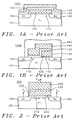
- Transistor 100b has a split channel consisting of a section 110 whose conductivity is controlled by floating gate 140 and control gate 145, in series with a section 118, whose conductivity is controlled by control gate 145.
- Passivation layer 900 is shown in Fig. 1B. In both type transistors 100a and 100b, programming takes place by injection of hot electron near the silicon surface and near the drain junction.
- Fig. 2 presents the cross sectional view of a typical double polysilicon stack gate EPROM transistor 200, which was used to explain his lucky model.
- the transistor is an NMOS transistor with source 204, drain 206, substrate 201, floating gate 240 and control gate 245.
- the electrons gain energy and momentum from the horizontal field reaching maximum energy near the drain edge 206.
- a small portion of electrons obtain higher energy than the tunnel oxide (220) barrier height.
- the insulator barrier height it becomes possible that electrons may be emitted into the insulator 220 and reach the floating gate polysilicon 240 if the momentum (motion) of electrons is redirected upward to the floating gate by acoustic phonon scattering without suffering energy loss. It was observed that the probability of injection from the channel into the polysilicon is less than the orders of IE-6 to IE-9. Also the model suggested that channel hot electron emission into a floating gate would be negligible if Vd-Vs is less than 2.5V, no matter how small the channel length or junction depth.
- EEPROM electrically erasable and programmable read-only memories
- electrons stored on the floating gate are removed electrically by applying the appropriate voltages to the transistor terminals.
- One approach is with the double polysilicon EEPROM cell, which removes electrons from the floating gate to downward silicon (i.e., either source, drain diffusions or substrate).
- Another approach is with the triple polysilicon EEPROM cell which removes electrons from the floating gate to a separate third gate.
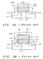
- FIG. 3A A typical double polysilicon stack gate EEPROM cell by H. Kume, which removeselectrons from floating gate to downward silicon, is shown in Fig. 3A.
- Erase in double polysilicon EEPROM transistor 300a is achieved through tunnel oxide 320, between floating gate 340 and source diffusion junction 304 when the electric field across the tunnel oxide exceeds the critical electric field for F-N tunneling of ⁇ 10 MV/cm.
- the tunnel oxide is 10nm
- the diffusion junction is 12V
- the control gate is 0V
- the drain voltage is floating. Since this approach requires high voltage on the source junction, the junction is susceptible to avalanche breakdown.
- This stack gate cell is a variation of EPROM cell 100a in Fig. 1A, but with an asymmetrical deep source junction. It is noted that the double poly split gate transistor 100b offers a junction on only one side and so cannot be used for EE applications requiring asymmetric diffusions.
- the triple polysilicon transistor overcomes this problem because electrons are not removed to the junction, but to a third polysilicon.
- the triple silicon EEPROM cell is claimed to solve the density disadvantages associated with a deep junction for scaled-down memory technologies.
- a triple polysilicon device is described by J. Kupec et al. in 1980 IEDM Technical Digest, p.602 in an article entitled, "Triple Level Polysilicon EEPROM with Single Transistor per Bit".
- An improvement to the Kupec device was proposed by F. Masuoka and H. Iizuka in US Pat No. 4,531,203 issued July 23, 1985. Variations on the same cell are described by C.K. Kuo and S.C. Tsaur in US Pat. No.
- All of these various triple polysilicon memory cells utilize one of the polysilicon levels as an erase gate.
- An erase gate passes through each memory cell transistor closely adjacent to the surface of the floating gate, but insulated therefrom by a thin tunnel dielectric. Charge is then removed from the floating gate to the erase gate, when appropriate voltages are applied to all of the transistor elements.
- the EEPROM transistor 300b with the third polysilicon for erase by Kupec is shown in Fig. 3B. In transistor 300b, electrons stored on the floating gate 340 are removed from the side wall of the floating gate to the third polysilicon 350.
- Typical voltages applied to each node during erase are the following: 12-15V on the triple erase polysilicon for 20nm ONO 325, and 0V for the second polysilicon of control gate 345 and the diffusion junctions of 304 and 306.
- the highest junction voltage is about 5V on the drain, during program.
- junction avalanche breakdown and junction leakage problems do not exist in the triple polysilicon EEPROM transistor.
- the solution of a triple polysilicon transistor has its own cost however. The disadvantages:
- This invention relates to an improvement for electrically programmable read-only memories (EPROM) and electrically erasable programmable read only-memories (EEPROM), specifically to device structures and operating techniques to effectively utilize the structure for extended applications in non-volatile memories.
- EPROM electrically programmable read-only memories
- EEPROM electrically erasable programmable read only-memories
- the invention also relates to methods for making such device structures.
- An electrically programmable read-only memory utilizes a floating (unconnected) conductive gate in a field effect transistor structure, positioned over but insulated from, a channel region on a semiconductor substrate, between the source and drain regions.
- a control gate is provided over the floating gate, but also insulated therefrom.
- the memory state is determined by the amount of charge retained on the floating gate, which controls the threshold characteristics of the transistor.
- the mechanism of the charge storage phenomena in channel hot electron (CHE) is explained by the following.
- the state of a memory cell transistor is read by placing a voltage across its source and drain, and on its control gate, the same way a normal MOSFET transistor is operated.
- the amount of current flow between the source and the drain is influenced by the threshold voltage, namely, the amount of stored electrons.
- the state of the memory is determined by the current level. Only a small portion of channel electrons are injected onto the floating gate, typically one out of millions. Programming time to inject electrons onto the floating gate is very slow, compared to the read time of the same memory transistor.
- high drain and control gate voltages are employed in EPROM and flash EEPROM cells. The requirement of high voltage is a major obstacle to scaling down the memory array.
- the present invention seeks to provide an improved memory device.
- an electrically programable memory device as specified in Claim 1.
- the present invention can provide a new memory cell configuration and structure which improves, by many orders of magnitude, the electron injection efficiency.
- the memory cell configuration and structure allows reliable, programming and reliable erasing from the same drain junction.
- the preferred embodiment can reduce the drain and control gate voltages necessary for electron injection, to allow future scaling of the memory cell and high density memories, as well as improve reliability and endurance of the memory cell. It can also provide faster programming time to attain the target level of electron storage, which, when combined with controllability of electron injection, makes applications of multi-level/multi-bit storage on a single memory transistor, more effective.
- Another embodiment provides a feature for EPROM function in a single polysilicon cell with a new structure and operating techniques of program and read for that singel polysilicon cell.
- an operating technique for tunneling erase from the floating gate to the control gate by utilizing a feature of the new structure as a double polysilicon EEPROM cell instead of the triple polysilicon EEPROM in prior art.
- An embodiment provides a feature for Non-Volatile RAM function in a split gate cell with a new structure, and provides an operating technique to write 'O' (program) or '1' (erase) for a selected word line (control gate).
- a single polysilicon EPROM cell can be achieved, distinguished from the prior art double polysilicon cell at low voltage programmability of as low as 5V, utilizing the first embodiment of a step channel/drain structure by simply adjusting the overlap drain region to be slightly longer than the horizontal channel length.
- the simplicity of the structure and its manufacturing process, as well as its low operating voltage makes the EPROM compatible with logic or DRAM and provides wider application such as intergration of EPROM onto a logic chip, or redundancy personalization to repalce aluminum or polysilicon fuses on a DRAM chip.
- a new feature of reliable erase and program operations at the same junction can be achieved by adjusting the N-drain length longer, junction depth deeper, and dosage lighter, to withstand the high voltage needed to induce tunneling from the floating gate to diffusion without adversely affecting the injection efficiency very much.
- a reliable erase operation by tunneling to diffusion is only implementable at the deep source side junction, and not at the shallow drain junction which is used for programming. Therefore a split gate structure, as well as a stack gate structure, can be adapted to use this feature, otherwise same side erase and program is impractical since the split gate cell has only one junction next to the floating gate.
- Another preferred feature for erase operation by tunneling from the floating gate to the control gate in a double polysilicon EEPROM transistor with a step channel/drain is also enabled by adjusting the length of overlapped floating gate over the N-drain diffusion.
- electron removal from the floating gate to another polysilicon by tunneling required a triple polysilicon structure instead of double in an EPROM transistor.
- This double polysilicon EEPROM transistor feature provides a shallower drain junction (compared to tunneling from floating gate to diffusion), reduced process complexity (double polysilicon vs. triple polysilicon), smaller erase block size such as by word line (control line) level, and extended endurance due to reduction of unnecessary program/erase cycles, resulting from the size of the large block erase.
- Non-volatile RAM operation using a split gate double poly transistor with a step channel/drain structure can be enabled by combining the operating features of low voltage programming and poly to poly tunnel erase.
- the nature of Random Access Memory is the capability to write "O"'s (program) and "1"'s (erase) to different transistor locations at the same time, for an electrically connected and selected control gate. With proper design and application of voltages on the drain and the source, RAM functionally can be achieved for a split gate double poly transistor with a step channel/drain structure. This double polysilicon split gate transistor with injection step channel will find much wider application since it behaves like RAM but is also non-volatile. Also, the bit by bit program and erase capability extends the endurance of program/erase cycles, as well as improves program/erase time.
- a triple polysilicon EEPROM transistor with an arbitrary vertical floating gate channel in series with a horizontal channel (without N-drain region but with vertical channel) can be provided, which is a variation of the double polysilicon EEPROM transistor with a step channel/drain and utilises the same concept of high injection efficiency due to straight injection of electrons, in the direction of movement, into the vertical component of the floating gate.
- a described embodiment demonstrates the manufacturability of the step channel device structure.
- a simple method to fabricate the step channel with self aligned N-drain to the step is first shown, in which the floating polysilicon gate to cover the step channel in a non-self aligning process.
- This simple method to create a step processes to fabricate stack and split gate transistors in EPROM/EEPROM are also shown.
- Fig. 1A is a cross section of the stack EPROM prior art cell which programs by injecting channel hot electrons into the floating gate.
- Fig. 1B is a cross section of the split EPROM prior art cell which programs by injecting channel hot electrons into the floating gate.
- Fig. 2 is a cross section of the stack EPROM prior art cell which is used to explain 'Lucky-Electron Model' of injecting channel hot electrons into the floating gate.
- Fig. 3A is a cross section of the stack EEPROM prior art cell which erases by tunneling of electrons from the floating gate to the source diffusion.
- Fig. 3B is a cross section of the flash EEPROM prior art cell with triple polysilicon which erases by tunneling from the floating gate to an erase gate.
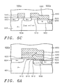
- Fig. 4A is a cross section of the stack gate EEPROM cell with a step channel/drain structure, in accordance with the first embodiment of this invention wherein channel hot electrons are injected straight in the direction of the moving electrons, into the floating gate through the side wall channel oxide.
- electrons on the floating gate are removed by tunneling from the floating gate to the step drain diffusion.
- Fig. 4B is a cross section of the split gate EEPROM cell with a step channel/drain structure, in accordance with the first embodiment of this invention wherein channel hot electrons are injected straight in the direction of the moving electrons, into the floating gate through the side wall channel oxide.
- electrons on the floating gate are removed by tunneling from the floating gate to the step drain diffusion.
- Fig. 4C is an illustration of the angle measurement of the step, which is measured from the channel silicon surface and is appropriately larger than 30 degrees, due to density considerations.
- Fig. 5A is a cross section of the single polysilicon EPROM cell with a step channel/drain structure in accordance with the second embodiment of this invention wherein channel hot electrons are injected straight in the direction of the moving electrons, into the floating gate through the side wall channel oxide.
- Fig. 5B is a cross section of a capacitor wherein the polysilicon gate is electrically connected to the floating gate polysilicon of the EPROM cell in Fig. 5A providing control/select gate function.
- Fig. 5C is a cross section of the EPROM memory cell wherein the EPROM transistor 500a in Fig. 5A is in series to a normal FET transistor 500cwhich provides the select function of memory transistor.
- Fig. 6A is a cross section of the stack gate EEPROM cell with a step channel/large overlapped drain structure designed for another feature of tunnel erase, in accordance with the fourth embodiment of this invention wherein electrons on the floating gate are removed by tunneling from the floating gate to the control gate, in addition to the feature of first embodiment of straight injection of electrons in the direction of moving via step channel oxide.
- Fig. 6B is a cross section of the split gate EEPROM cell with a step channel/large overlapped drain structure designed for another feature of tunnel erase, in accordance with the fourth embodiment of this invention wherein electrons on the floating gate are removed by tunneling from the floating gate to the control gate. Also this transistor is operated as a Nonvolatile RAM by proper designs and conditions which is the fifth embodiment of this invention.
- Fig. 6C is a cross section of another split gate EEPROM cell structure with a step channel, which is a variation of, and operates with identical functionality to, the transistor 600b in Fig. 6B.
- Figs. 6D and 6E are variations of the double polysilicon split gate transistor of Fig. 6B with the step channel.
- Fig. 7A is a simplified capacitance model for the transistors in Figs. 6A, 6B, 6C, 6D ,6E to explain the operation of poly tunnel erase EEPROM and Non-volatile RAM.
- Fig. 7B contains Table which shows example voltage conditions for writing '0' and '1' for Non-volatile RAM operation in accordance with the fifth embodiment of this invention.
- Fig. 8A is a cross section of the triple polysilicon split gate EEPROM cell with a vertical (step) long channel for floating gate, in accordance with the sixth embodiment of this invention wherein channel hot electrons are injected straight in the direction of the moving electrons from source, into the floating gate through the vertical channel oxide. Electrons on the floating gate are removed by tunneling from the floating gate to the drain diffusion or from the floating gate to the select gate.
- Fig. 8B is a cross section of the triple polysilicon split gate EEPROM cell with a vertical channel for normal gate, which is a variation of transistor Fig. 8A, in accordance with the sixth embodiment of this invention wherein channel hot electrons are injected straight in the direction of the moving electrons from source, into the floating gate through the horizontal channel oxide. Electrons on the floating gate are removed by tunneling from the floating gate to the drain diffusion.
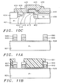
- Figs. 9A and 9B are cross-sections of the forming step channel with a self aligned drain n-diffusion during key stages in manufacturing process example in accordance with the seventh embodiment of this invention.
- Figs. 9C and 9D are cross-sections of the fonning stack gatc cell of Fig. 4A, Fig. 5A and Fig. 6A during various stages of the manufacturing process.
- Fig. 10A through 10C are cross-sections of the forming split gate cell of Fig. 4B, and Fig. 6B during various stages of the manufacturing process.
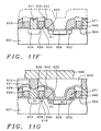
- Fig. 11A through 11G are cross-sections during the formation of the split gate of Fig. 6C, during various stages in the manufacturing process, in which the horizontal floating channel is at least 150nm.
- Fig. 11G is a crossectional view taken along the line 11G - 11G' of Fig. 11H.
- Fig. 11H is a top view of the split gate With the step injection channel.
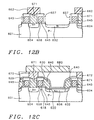
- Figs. 12A through 12C are cross-sections during the formation of the split gate of Fig. 6C, during various stages in the manufacturing process, in which the horizontal floating channel is less than 100nm.
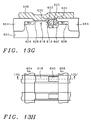
- Figs. 13A through 13G are cross-sections of transistor 600d and transistor 600e, during various stages ofthe manufacturing process.
- Fig. 13G is a crosssectional view taken along the line 13G - 13G' of Fig. 13H.
- Fig. 13H is a top view of transistor 600d in a memory array, after completion of process.
- Transistor 400a in Fig. 4A has a p-type silicon substrate 401 (which can alternatively be a ptype epitaxial layer grown on top of a p+ doped silicon substrate), N+ source diffusion 404, a horizontal channel region of 410, a step channel 413, a drain diffusion 406, a control gate 445, and a floating gate 440 which uniformly covers both the horizontal and step channel.
- the floating gate is dielectrically isolated from the surface of the silicon substrate by dielectric film 420, which is thermally grown dioxide.
- Control gate 445 is capacitively coupled to floating gate 440 through dielectric film 430, which can either be thermally grown silicon dioxide or a combination of thin layers of silicon dioxide and silicon nitride.
- P-type 401 is typically doped in the range of between about 1E16cm-3 to 5E17cm-3
- dielectric film 420 is typically 5 to 10 nanometers thick
- floating gate 440 is usually a heavily N+ doped film of polysilicon of a thickness which can be as low as 100nm or as high as 300nm.
- Control gate 445 is either a heavily N+ doped film of polysilicon or a low resistivity interconnect material like silicide, or another refractory material.
- N+ source diffusion 404 is formed by ion implantation of Arsenic, Phosphorus, or Antimony.
- N+ drain 402 is formed by the same ion implant material, but self-aligned to step channel edge 413, immediately after formation of step and prior to formation of oxide layer 420.
- the angle of the step measured from the horizontal plane of the original silicon surface as illustrated in Fig. 4C is not critical as long as a reasonable area of more than 20 nm in vertical depth is exposed for injection. If the angle is too small , the length of step channel region gets too long, which is a density penalty. Therefore it is reasonable that the step angle will be greater than 30 degrees.
- the depth of this step 413 is at least 20 nm or larger. The purpose of the step 413 is to inject hot electrons more efficiently onto floating gate 440.
- control gate 445 When a proper voltage level is applied to control gate 445, the floating gate potential which is capacitively coupled to the control gate becomes higher than the threshold voltage in the horizontal channel region 410 and electrons are supplied into channel from source junction 404. The electrons are then accelerated by the horizontal drain field, as in a MOSFET transistor, when the drain diffusion 406 is biased with a positive voltage. Electrons flow near the silicon surface within an inversion layer of horizontal channel region 410 (typically within 10 nm).
- the N-drain covers the corner of channel 415 with proper doping concentration(typically in the order of 1E18 per cm-3), maximum electric field can be created near the corner 415, along the side channel 413, which becomes the injection point because the electrons reach maximum speed and the momentum of the electrons is still close to horizontal.
- the energy level of electrons gained in the channel transport is higher than the barrier height (3eV for silicon dioxide) and the floating gate potential is higher than the potential at the comer 415, the high energy electrons penetrate straight into the floating gate.
- prior art relied on the indirect process of electron scattering by phonon and the 90 degree upward redirection of motion to the floating gate without suffering energy loss in conventional CHE EPROM.
- the configuration ofthis invention's step structure enhances the efficiency of electron injection from the channel to the floating gate by many orders magnitude.
- the present invention of EPROM structure has a high efficiency injection of hot electrons onto the floating gate, obtained by a drain voltage of around 3V, which is significantly lower than the 5V required for the low injection efficiency of prior art EPROM cells. Therefore the control gate voltage required for the present invention EPROM cell is proportionally reduced from 9v to 5v. High injection at lower voltage eliminates all the disadvantages listed in the section, "Description of Prior Art".
- the drain voltage of the present invention can be as low as the theoretical limit of 2.5 ⁇ 3.0V which is almost half of the prior art EPROM requirement, since enough hot electron emission is already achieved by the high injection efficiency.
- the control voltage for the present invention is also reduced proportionally to the reduction of drain voltage, which is almost halved.
- the program time to store a target level of injection electrons onto the floating gate can be reduced, due to high injection efficiency by the present invention.
- Multi-level storage on the floating gate becomes easier since the program time to achieve the target level set by the control gate voltage is shorter.
- the oxide thickness and the channel length of high voltage periphery circuits can be significantly reduced due to the reduced voltage requirement for the control gate.
- the power consumption during programming is improved by many orders of magnitude, due to high injection efficiency and lower voltage operation, a very attractive feature in portable operation.
- a single polysilicon n-channel EPROM cell distinguished from prior art by low voltage programmability is achieved.
- Low voltage operation of less than 5V is attractive since the processes needed for high voltage devices with thick oxide and drain engineering can be eliminated.
- Figs. 5A, 5B and 5C presents cross-sectional views of a single polysilicon n-channel EPROM transistor in accordance with a second embodiment of this invention.
- the transistor is a modification of transistor 400a, in which the second polysilicon has been eliminated, and the dimension of the gate overlapping the drain Ln region has been adjusted.
- Transistor 500a has ptype substrate 501, N+ source diffusion 504, a channel region of horizontal 510, step 513, N-drain diffusion 502, N+ drain 506, and a floating gate 540 which uniformly covers both the horizontal and step channels.
- Floating gate 540 is dielectrically isolated from the surface of the silicon substrate by dielectric film 520, which is thermally grown dioxide.
- the passivation layer 900 is the same as mentioned during the first embodiment.
- p-type 501 is typically doped in the range of 1E16cm-3 to 5E17cm-3.
- the dielectric film 520 is typically 5 to 10 nanometers thick, and the floating gate 540 is usually a heavily N+ doped film of polysilicon with a thickness range of 100nm to 400nm.
- N+ source diffusion 504 is formed by ion implantation of Arsenic, Phosphorus, or Antimony.
- N drain 502 is formed by the same implant material, but self-aligned to the step channel edge 513 immediately after formation of the step, and prior to formation of oxide layer 520.
- the concentration of 502 under the floating gate region is in the range of 1E18 ⁇ 5E19cm-3, slightly lower than diffusion junction 504/506's concentration, which is greater than 5E20 cm-3.
- the angle of the step, measured from the horizontal plane, is preferable larger than 30 degrees.
- the depth of step 513 is 30nm or more.
- the purpose of step 513 is to inject hot electrons more efficiently onto floating gate 604, at the corner of step channel 515.
- the program conditions of electron injection onto floating gate are the same as described in the first embodiment, "EPROM N-channel transistor with step channel at drain edge": (1) The potential at the injection point 515 > 2.5V ⁇ 3.0V and (2) the floating gate potential 2.5V ⁇ 3.0V is higher than the voltage at the injection point.
- the first condition (1) is easily achieved by applying a drain voltage greater than 3V.
- the second condition in which the floating gate potential must be greater than 2.5V ⁇ 3.0V, can be obtained by two approaches.
- the first approach specifies that the length of Ln (502) be slightly longer than the horizontal channel region length (510), which increases the drain-to-floating gate coupling capacitance. In this case, when 5V is applied to the drain 506, the floating gate voltage reaches 2.5V ⁇ 3.0V.
- the second approach forms coupling capacitance 500b outside of the EPROM transistor as shown in Fig. 5A with the gate of capacitor 541 being the same polysilicon as floating gate 540 and connected electrically each other.
- the Ln length can be minimal, since the floating gate voltage is rasied by coupling from the external capacitor.
- the area of coupling capacitance is designed to be slightly larger than the EPROM transistor gate area, to achieve a coupling ratio of 0.6.
- the external capacitor acts in the same function on the control gate in the double polysilicon EEPROM memory cell.
- the transistor has a function of storage but it does not have a function of select. Therefore, in order to use this device as an EPROM memory cell, a conventional n-channel FET device 500c is added in series to this single EPROM transistor 500a as shown in Fig. 5A.
- the gate of the conventional FET transistor 500c provides the select function (control gate) to access the information on the storage transistor 500a.
- the storage EPROM transistor is normally 'on' (depletion device by implanting the channel region 510 with Arsenic or phosphorus, concentration of 5E16 to 5E17/cm3). After storing injected electrons, the threshold voltage is increased and the 'off' condition is obtained.
- a single polysilicon n-channel EPROM cell distinguished from prior art by a step injection channel, provides low voltage programming as low as 5V.
- the advantages obtained from this single poly EPROM are (i) the elimination of the double polysilicon requirement, (ii) the elimination of high voltage devices (iii) EPROM compatibility with Logic or DRAM due to process simplification from this elimination of double polysilicon and high voltage devices (iv) wider application such as integration of EPROM onto a logic chip, as well as redundancy personalization to replace fuses on a DRAM chip.
- Transistor 400a in Fig. 4A is a modification of the double polysilicon EEPROM transistor 300a in Fig. 3A, in which the drain junction is replaced by a step channel/drain, and the depth ofsource junction 404 is reduced.
- the source junction depth can be reduced because erase is done at the side of the step channel/drain instead of the source side.
- the step junction is also already equipped with a lightly doped junction for an improved ability to withstand 10-12V before breakdown.
- Both transistors 400a and 400b consist of a p-type silicon substrate 401, N+ source diffusion 404, a channel region of horizontal 410 of which conductivity is controlled by floating gate 440, a control gate 445, a step 413, a N-drain diffusion 404, N+ drain diffusion, a floating gate 440 uniformly covering both the horizontal and step channel, and a control gate 445.
- Split gate 400b has an extra channel region 418 the conductivity of which is controlled by control gate 445 in series with a section of channel 410.
- the floating gate is dielectrically isolated from the surface of the silicon substrate by dielectric film 420, which is thermally grown dioxide.
- Control gate 445 is capacitively coupled to floating gate 440 through dielectric film 430, which can be either thermally grown silicon dioxide or a combination of thin layers of silicon dioxide and silicon nitride.
- P-type 401 is typically doped in the range of 1E16cm-3 to 5E17cm-3
- dielectric film 420 is typically 5 to 10 nanometers thick
- floating gate 440 is usually a heavily N+ doped film of polysilicon, the thickness of which can be as low as 100nm or as high as 300nm.
- Control gate 445 is either a heavily N+ doped film of polysilicon, low resistivity interconnect material like silicide, or a refractory material.
- N+ diffusions 404 and 406 are formed by ion implantation of Arsenic, Phosphorus, or Antimony.
- N-drain 402 is formed by the same ion implant material, but self aligned to step channel edge 413, immediately after formation of the step, and prior to formation of oxide layer 420.
- the N-junction 402 for 10V erase is typically doped in the range of 1E17 to 1E18 cm-3 and its depth is chosen to be 250 to 300nm, which is slightly deeper than the source junction of 150 to 200 nm.
- the erase operation is basically the same as explained for transistor 300a, which is the most commonly used transistor in industry practice. Assuming a tunnel oxide 410 of 9 nm, an ONO of 20nm and a coupling ratio of 0.55, when ⁇ 10V is applied to the drain junction and 0V is applied to the control gate in either transistor 400a and 400b, the electric field across the oxide 422 exceeds the critical value of F-N tunneling, which is ⁇ 10 MV/cm. Electrons stored on the floating gate are then released to drain junction by F-N tunneling, which is implemented at the source side in transistor 300a, but at the drain side in this step channel/drain transistor. Since this approach requires high voltage on the drain junction, the drain junction is susceptible to the avalanche breakdown.
- the N-junction 402 is lightly doped and deeper than source junction 404.
- the invention of an operation of program and erase using the same step channel/drain junction is achieved.
- a split gate structure as well as a stack gate structure is able to be implemented with a double polysilicon EEPROM transistor by this invention.
- tunnel gate oxide 620 is in the range of 5 to 10 nm
- dielectric 630 such as ONO or nitrided oxide is about equal to or thicker than tunnel oxide, typically 8 to 15 nm and
- the lengths of channel region 610 and overlap diffusion Ln 602 are roughly the same.
- Typical critical electric fields for tunneling from polysilicon to polysilicon through ONO which is a thermal oxide over polysilicon or CVD deposited oxide/nitride, are reported to be about 6 MV/cm (lower when compared to the electric field for a thermally grown substrate oxide of 10 MV/cm in E. Harari and F. Masuoka). Therefore, the electric field across dielectric 630 must be more than 6 MV/cm for tunnel erase from the floating gate to the control gate. On the otherhand, the electric field across the ONO during channel hot electron injection must be maintained to be less than 3 MV/cm, considering process noise margins and residual charge. In transistors 600a and 600b, operation and design of the double polysilicon EEPROM are illustrated using a simple model.
- a simplified capacitance model for transistors 600a and 600b is provided in Fig. 7A.
- the capacitor Ccg-fg is the capacitance between the control gate 645 and the floating gate 640.
- Cfg-Ln is the capacitance between floating gate 640 and the underneath n-diffusion region 602.
- Cfg-ch is the capacitance between the floating gate 640 and the channel region 610 (in more accurate predictions, source to floating gate overlap capacitance in Cfg-ch also needs to be included for the stack gate cell).
- all three capacitances are chosen to be equal, which makes the explanation easier, but the assumption is also practical and reasonable.
- Transistors 600c, 600d, and 600e shown in Figs. 6C, 6B and 6C are variations of the double poly split gate transistor 600b with the step channel. Programming and erase for all these transistor variations utilize the same electron injection mechanism as previously explained for transistor 600b.
- the floating gate of transistor 600c is formed on the sidewall of the split gate, as shown in Fig. 6C.
- the coupling capacitor is obtained through sidewall, between the split gate and the floating gate.
- erase is performed by tunneling through the sidewall.
- the floating gate in transistor 600d is recessed into the silicon surface.
- Transistor 600e has the recessed floating gate of transistor 600d, but the function of N+ drain 606 is combined into the 602 region with a penalty of higher sheet resistance. This transistor 600e can be used to build high density memory arrays, when placed in series.
- the concept of operation and design as Random Access Memory is the fifth embodiment of this invention.
- tunnel gate oxide 620 thickness is in the range of 5 to 10 nm
- dielectric 630 such as ONO or nitrided oxide is equal to or thicker than tunnel oxide thickness, which is typically 8 to 15 nm
- the lengths of channel region 610 and the overlap diffusion Ln 602 are roughly same.
- Typical critical electric fields for tunnel from polysilicon to polysilicon through ONO which is a thermal oxide over polysilicon or CVD deposited oxide/nitride are reported about 6 MV/cm (lower than when compared to a thermally grown substrate oxide of 10 MV/cm in E. Harare and F. Mazurka). Therefore, the electric field across the dielectric 630 must be more than 6 MV/cm for tunnel erase from floating gate to control gate. On the otherhand, the electric field across the ONO during Channel Hot Electron Injection must be maintained to be less than 3 MV/cm, considering process noise margin and residual charge. In double polysilicon EEPROM transistor 600b, operation and design of non-volatile RAM is illustrated using a simple model.
- a simplified capacitance model of transistor 600b is provided in Fig. 7A.
- the capacitor Ccg-fg is the capacitance between the control gate 645 and the floating gate 640.
- Cfg-Ln is the capacitance between floating gate 640 and the underneath n-diffusion region 602.
- Cfg-ch is the capacitance between floating gate 640 and the channel region 610.
- all three capacitances are chosen to be equal, which makes the explanation easier, but the assumption is provides a practical and reasonable operating point.
- more precise optimization can be obtained by extending the concept utilizing more detailed modeling.
- the tunnel gate oxide is 8 nm
- the ONO is 11 nm
- write operating voltage conditions are met
- the resulting floating gate potential and the electric field across the ONO are summarized in the Table given in Fig. 7B for write "0", "1" and "no change".
- the control gate voltage is 5V when unselected and 10V when selected.
- the electric field across the ONO is always kept below 3 MV/cm except during erase, which is safe enough below the critical tunnel field of 6 MV/cm.
- a "0" or “1” can be written at any time by choosing the appropriate voltages for the drain and source as long as the control gate is selected and raised to 10V.
- the operation of writing "0'''s and “1"s in random access memory, namely, program and erase at the same time and at different transistor locations for an electrically connected and selected control gate, is achieved by choosing proper voltages on the drain and source in exactly the same manner that a bit line is selected in Random Access Memory.
- non-volatile RAM capability not achievable in prior art EEPROM, is enabled in the present invention transistor for a split gate double polysilicon transistor.
- FIG. 8A and Fig. 8B presents a cross-sectional view of a triple polysilicon EEPROM transistor with an arbitrary vertical floating gate channel in series to horizontal channel.
- Transistors 800a and 800b consist of p-type silicon substrate 801, N+ source diffusion 804, a channel region of horizontal 818 whose conductivity is controlled by a third polysilicon for the select gate (word line).
- the vertical channel 810 is controlled by floating gate 840 and control gate 845.
- the floating gate 840 covers only the vertical channel and a drain diffusion 806 at bottom of the vertical trench.
- the floating gate is dielectrically isolated from thermally grown silicon dioxide 820.
- Control gate 845 is capacitively coupled to floating gate 840 through dielectric film 830, which can be either thermally grown silicon dioxide or a combination of thin layers of silicon dioxide and silicon nitride.
- P-type 801 is typically doped in the range of 1E16cm-3 to 5E17cm-3
- vertical gate dielectric film 820 is typically 5 to 10 nanometers thick
- the horizontal channel gate oxide is slightly thicker at 8 to 15 nm
- floating gate 840 is usually a heavily N+ doped film of polysilicon with a thickness that can be as low as 100nm or as high as 300nm.
- Control gate 845 is a heavily N+ doped film of polysilicon.
- the select gate 850 is polysilicon or a low resistivity interconnect material like silicide, or a refractory material.
- N+ source diffusion 804 and is formed by ion implantation of Arsenic, Phosphorus, or Antimony.
- N+ drain 806 is formed by the same ion implant material, but self-aligned to the vertical channel edge 810, immediately after formation of the step, and prior to deposition of floating gate polysilicon 840.
- the junction 806 is doped with phosphorus as well as Arsenic to increase junction depth for higher junction breakdown.
- the drain junction depth can be a normal Arsenic-doped junction.
- the channel electrons are supplied from N+ junction 804, but the electrons can be inverted layers of channel electrons instead of N+ junction as long as it supplies electrons into the select gate channel.
- control gate 845 When a certain voltage level is applied to control gate 845, the floating gate potential which is capacitively coupled to the control gate becomes higher than the threshold voltage in the vertical channel region 810, and electrons start flowing from source junction 804 to drain junction 806, if select gate 850 is also raised higher than the threshold voltage. The electrons are then accelerated by the horizontal field, as in a MOSFET transistor.
- control gate 845 When control gate 845 is biased high enough to raise the floating gate potential higher than the sum of the drain and threshold voltages, the channel potential at 815 approaches the voltage applied to drain 806, as long as select gate 850 is biased slightly higher than the threshold voltage and the horizontal channel resistance is high compared to the vertical channel resistance. Then, maximum electric field is created at the intersection 815 of the horizontal and vertical channel, which becomes the injection point because electrons reach maximum speed and the momentum of the electrons is still horizontal. When the energy level of electrons gained in channel transport is higher than the barrier height, high energy electrons penetrate straight into the floating gate. In contrast, prior art relied on the indirect process of electron scattering by phonon and 90 degree redirection upward to the floating gate. Thus the configuration of this vertical channel structure enhances the efficiency of electron injection from the channel to the floating gate by many orders of magnitude.
- the prime objective of this invention is to introduce a new configuration for the EPROM device structure, and device operations for EPROM, EEPROM and NVRAM transistors with the new structure.
- Another objective is to demonstrate methods to fabricate the structure. A few approaches from among many possible methods to fabricate the step channel at drain edge, are described.
- the first approach is a simple non-self aligned method to cover the channel step with a floating gate polysilicon.
- the second approach is to minimize the misalignment during the masking process in the first non-self-alignment approach.
- Fig. 9A and Fig. 9B show the fabrication method for the step channel/drain structure in accordance with seventh embodiment of this invention.
- Step formation starts immediately after device isolation of LOCOS or shallow trench isolation 454, as shown in Fig. 8A.
- the device area is still covered with a dielectric 452 of thin silicon oxide and CVD deposited nitride.
- Photoresist 462 in Fig. 8B is applied and defined for the step region.
- the dielectric layer 452 is etched by dry RIE or wet etch like KOH. Then the silicon substrate is carefully etched at least 30nm.
- the angle of the step should be maintained to be greater than 30 degrees in order to achieve high injection efficiency, by injecting electrons directly with horizontal momentum into the floating gate.
- the angle can be controlled by setting the etching conditions in RIE.
- n-region 402 is implanted by self alignment to drain edge 415 with a species of Arsenic, Phosphorus or Antimony.
- the implant dosage for the n-region is less than 5E19 cm-3, in order to maintain good gate oxide quality and to control channel oxide thickness over step 413.
- a structure of an n-junction self-aligned to the step channel/drain region is achieved with this simple process.
- the tunnel oxide 420 is thermally grown. After this formation of step channel/drain, the normal EEPROM process follows.
- the methods to fabricate transistor 400a in Fig. 4A and transistor 600a in Fig. 6A are provided next.
- the difference between the two transistors is simply in the N-drain junction.
- the N-drain in transistor 400a is designed for a high voltage during tunnel erase from the floating gate to its N-drain. Therefore the N-drain junction in transistor 400a is deeper than that of 600a, obtained by the implant of high diffusitivity, Phosphorus with the dosage range of SE13/cm 3 ⁇ 5E14/cm 3 and at the energy range of 100 keV ⁇ 180 keV.
- the N-drain in transistor 600a is formed with a reduced energy in the range of 30 keV ⁇ 100keV for Phosphorus ion implant.
- Arsenic can also be used for the N-drain in transistor 600a.
- the N-drain junction depth for transistor 600a is as shallow as the Arsenic source junction.
- Floating gate polysilicon 440 is deposited over the thermally grown tunnel oxide 420 and thin oxide is grown over the polysilicon layer.
- photoresist mask 464 for floating gate separation from the adjacent cell (in the vertical dimension) is applied, shown in Fig. 9C, as floating gate definition over isolation oxide 454.
- a composite dielectric layer 430 such as ONO or nitrided oxide is deposited and followed by second control gate polysilicon 445. After formation of dielectric layer 454 over control gate polysilicon, photoresist mask 466 in Fig.
- 9D defines the control gate and floating gate by careful reactive ion etching followed by ion implantation of the source/drain junction region. Normal FET processes follow such as sidewall spacer formation, diffusion annealing, passivation, contact hole opening, and metalization for wiring. Thus, the final device structures for stack transistors 400a in Fig. 4A and transistor 600a in Fig. 6A are obtained.
- split gate transistors 400b and 600b with the step channel/drain, there is no difference the fabrication of the two transistors from commonly practiced split gate processes, after formation of the step channel.
- N-drain junction requirements are different between the transistors.
- the N-drain in transistor 400b is designed for a high voltage during tunnel erase from the floating gate to its N-drain. Therefore the N-drain junction in transistor 400b is deeper than that of 600b, obtained by the implant of high diffusitivity, Phosphorus with the dosage range of 5E13/cm 3 ⁇ 5E14/cm 3 and at the energy range of 100 keV ⁇ 180 keV.
- the N-drain in transistor 600b is formed with a reduced energy in the range of 30 keV ⁇ 100keV for Phosphorus ion implant.
- Arsenic can also be used for the N-drain in transistor 600b.
- the N-drain junction depth for transistor 600b is as shallow as the Arsenic source junction.
- the floating gate is defined first as shown in Fig. 10A 464, instead of separating between adjacent cells in stack gate transistor in Fig. 9C (shown as floating gate definition over field oxide).
- Photoresist mask 465 in Fig. 10B to form the N+ junction is inserted prior to the second polysilicon definition, followed by ion implantation with the species of Arsenic, Phosphorus or Antimony.
- split gate channel gate oxide and poly oxide are thermally grown. Then, a composite dielectric layer such as ONO or nitrided oxide followed by second control gate polysilicon 445 in Fig. 10C are deposited.
- the dosage of N+ for 404 is chosen to be relatively high, in the range of 5E20 to 5E21 cm-3, to grow oxide 424 thicker over N+ diffusion 404, compared to gate oxide 428 over the split channel 418 in Fig. 10C.
- photoresist mask defines at the same time the control gate and floating gate, separating adjacent cells over the field oxide by careful reactive ion etch. Sidewall spacer formation and diffusion annealing, passivation, contact hole opening and metalization for wiring in the normal FET process, follows.
- the final device structures for split gate transistor 400b in Fig. 4A and transistor 600b in Fig. 6A are obtained.
- step channel with a self-aligned diffusion of high injection area can be achieved by simple processes for transistors 400a, 400b, 600a and 600b. Once the step channel/drain is formed, existing fabrication processes for the stack gate transistor and split gate transistor follow.
- the second approach is a fabrication method for the split gate transistor 600c with precisely controlled lengths of horizontal channel and overlapped LNG under the floating gate. Two fabrication methods are described: the first, for a relatively large horizontal channel under the floating gate and the next for a minimal length of the horizontal channel length.
- Fig. 11A through Fig. 11G shows a fabrication method of a variation of a split gate transistor 600c with a step channel/drain structure in accordance with the above embodiment of this invention. After device isolation of LOCOS or shallow trench isolation, word line gate 645 (equivalent in function to the split gate channel 618 in transistor 600b) is defined as shown in Fig.
- the height of the polysilicon 645 is about 250 nm to 400 nm and the polysilicon is covered with a dielectric layer 655 of 100 to 200 nm.
- a thin oxide (10-20 nm) 656 is thermally grown over poly sidewall and followed by thin nitride 657 deposition by Chemical Vapor Deposition in Fig. 11B.
- Photoresist 661 is applied to define contact area. Using the photoresist mask, the nitride film 657 is isotropically etched by RIE and ion species of Arsenic is implanted to form the N+ source junction. After removing the photoresist, the side wall oxide (50- 80 nm) 658 in Fig.
- 11C is thermally grown selectively in the contact hole area which is several times thicker than that for 656 of the other side of polysilicon gate 645.
- the bottom oxide of contact hole is vertically etched by RIE, during which, the nitride 656 prevents oxidation of the area underneath and also acts as an etch stop during etching of the oxide over junction N+ 604.
- Polysilicon 670 with a thickness of 180-200 nm is deposited as shown by dotted line in Fig. 11D.
- Directional dry etch is performed to form sidewall spacer 672, which determines horizontal channel length 610 under the floating gate.
- the gate width and space 645 is 0.3 um, so the contact opening after thick side wall oxidation 658 is about 0.25 um. Therefore, the contact hole 671 is still completely filled with this polysilicon even after poly sidewall etching when the polysilicon 670 is thicker than 150 nm.
- the filled polysilicon is used to form the self aligned contact.
- Phosphorus for N-drain 602 is implanted with a dosage in the range of 1E14-7E15 per cm 2 at 50-100 keV. Then the thin nitride layer 657 is etched directionally using poly spacer 672 as a etching mask.
- the cross sectional view at this point looks like the figure in Fig. 11D.
- the combination of creating the horizontal channel, filling the contact hole and providing self aligned borderline contacts by one polysilicon deposition is one of unique features in this process.
- Photoresist 662 is provided to protect polysilicon in the contact hole during removal of the sidewall polysilicon, which was used to define the step and self aligned N-drain region 602 in Fig 11E.
- Thin nitride 657 is used to define thermal oxide underlayer 656. Then nitride 657 is removed selectively and isotropically by Chemical Dry Etch. Vertical dry etching of the silicon substrate is continued to create about a 50 nm step. At this point, the cross-section is as viewed in Fig.
- the oxide 656 is wet etched in a diluted buffer of HF solution.
- Thermal oxide 50-100 nm
- the oxide layer is nitrided in a N 2 O environment and another oxidation is repeated to minimize the pin hole.
- a thin CVD nitride layer (about 6 nm) can be deposited.
- floating gate polysilicon is deposited conformally by CVD and vertically etched by RIE as shown in Fig. 10F.
- the thickness ofthe polysilicon dictates the sidewall dimension, which defines the floating gate length. Since the CVD thickness is controlled very tightly (within 5%), the dimensions of horizontal channel length and Ln length are very accurately defined, to meet the precise design goals, by these two sidewall process.
- the objective of nitridation and presence of the nitride layer over poly side wall oxide 630 is to reduce leakage current between word gate 645 and floating gate 640, in order to improve retention time.
- the silicon nitride can be also be replaced by a silicon rich silicon oxide to reduce the tunnel erase voltage.
- the floating gate and the contact poly between adjacent cells are separated at the same time by using a photoresist mask (like the slit mask in a conventional floating gate EEPROM process) and by careful reactive ion etch marked as 640S and 671S in Fig. 11H.
- thermal oxidation of poly silicon floating gate and deposition of CVD oxide and nitride composite layer 629 follows.
- the purpose of composite layer 629 is to protect the floating gate polysilicon 640 from contamination and moisture. Normal process follows: deposition of a passivation layer such as jphosphosilicate glass (PSG), planarization by Chemical Mechanical Polish, opening of the contact hole, filling of the contact hole by W or Al or Cu, and metalization for wiring.
- the cross sectional view after processing is shown in Fig. 11G.
- the bird's eye or top view of the memory cell is shown in Fig. 11H.
- a structure of self aligned n-junction to step channel/drain region is achieved with this simple process.
- channel length, horizontal channel and step N-drain lengths under the floating gate of the split gate can be precisely defined by sidewall techniques. Also the polysilicon used to define the horizontal channel under the floating gate is also utilized to fill the self aligned contact hole.
- Figs. 12A through Fig. 12C show a fabrication method of a variation of the split gate transistor 600c with a step channel/drain structure, wherein the horizontal channel length under the floating gate is very small, typically less than 100nm compared to the previously large horizontal channel length (larger than 150nm). The processes of these two transistors is very similar.
- word line gate 645 (equivalent in function to the split gate channel 618 in transistor 600b) is defined as shown in Fig. 11A where the height of the polysilicon 645 is about 250 nm to 400 nm and the polysilicon is covered with a dielectric layer 655 of 100 to 200 nm. Then a thin oxide (10-20 nm) 656 is thermally grown over polysilicon sidewall and followed by thin silicon nitride 657 deposition by Chemical Vapor Deposition in Fig. 11B. Here, the nitride thickness determines the horizontal channel length (less than 100nm). Photoresist 661 is applied to define contact area.
- the nitride film 657 is isotropically etched by RIE and ion species of Arsenic is implanted to form the N+ source junction.
- the side wall oxide (50- 80 nm) 658 in Fig. 11C is thermally grown selectively in the contact hole area which is several times thicker than that for 656 of the other side of polysilicon gate 645.
- the bottom oxide of contact hole is vertically etched by RIE, during which, the nitride 656 prevents oxidation of the area underneath and also acts as an etch stop during etching of the oxide over junction N+ 604.
- Polysilicon 670 with a thickness of 180-200 nm is deposited as shown by dotted line in Fig. 11D.
- Directional dry etch is performed to form sidewall spacer 672.
- the gate width and space 645 is 0.3 um, so the contact opening after thick side wall oxidation 658 is about 0.25 um. Therefore the contact hole 671 is still completely filled with this polysilicon even after poly sidewall etching when the polysilicon 670 is thicker than 150 nm.
- the filled polysilicon is used to form the self aligned contact.
- Photoresist 662 is provided to protect polysilicon in the contact hole during removal of the sidewall polysilicon.
- nitride 657 is vertically etched and the nitride spacer shown by the dotted line in Fig. 12B is used to define the thermal oxide under layer 656. Then nitride 657 is removed selectively and isotropically by Chemical Dry Etch. After defining the step, Phosphorus for N-drain 602 is implanted with a dosage in the range of 1E14-7E15 per cm 2 at 50-100 keV. Vertical dry etching of the silicon substrate is continued to create about a 50 nm step. At this point, the cross-section is as viewed in Fig. 12B. After removing photoresist 662, the oxide 656 is wet etched in a diluted buffered HF solution.
- Thermal oxide (50-100 nm) is grown over the channel region 620 and the sidewall of polysilicon 630 (sidewall oxide over poly is slightly thicker than that over single crystal silicon substrate).
- the oxide layer is nitrided in a N 2 O environment and another oxidation is repeated to minimize the pin hole.
- a thin CVD silicaon nitride layer (about 6 nm) can be deposited.
- floating gate polysilicon is deposited conformally by CVD and vertically etched by RIE as shown in Fig. 12C. The thickness of the polysilicon dictates the sidewall dimension, which defines the floating gate length.
- the CVD thickness is controlled very tightly (within 5%), the small dimensions of horizontal channel length and Ln length are very accurately defined, to meet the precise design goals, by these two sidewall process of nitride and polysilicon.
- the objective of nitridation and presence of the nitride layer over poly side wall oxide 630 is to reduce leakage current between word gate 645 and floating gate 640, in order to improve retention time.
- the nitride can be also be replaced by a silicon rich oxide to reduce the tunnel erase voltage.
- the floating gate and the contact poly between adjacent cells are separated at the same time by using a photoresist mask (like the slit mask in a conventional floating gate EEPROM process) and by careful reactive ion etch marked as 640S and 671S in Fig. 11H.
- a photoresist mask like the slit mask in a conventional floating gate EEPROM process
- reactive ion etch marked as 640S and 671S in Fig. 11H Then thermal oxidation of poly silicon floating gate and deposition of CVD oxide and nitride composite layer 629 follows.
- the purpose of composite layer 629 is to protect the floating gate polysilicon 640 from contamination and moisture.
- a passivation layer such as PSG, planarization by Chemical Mechanical Polish, opening of the contact hole, filling of the contact hole by W or Al or Cu, and metalization for wiring.
- the bird's eye or top view of the memory cell is exactly the same as shown in Fig. 10H.
- a structure of self aligned n-junction to step channel/drain region is achieved.
- channel length, horizontal channel and step N-drain lengths under the floating gate of the split gate can be precisely defined by two sidewall techniques.
- Self aligned contacts filled with polysilicon are also provided.
- Fig. 13A through Fig. 13G show a fabrication method for transistors 600d and 600e, which are also variations of transistor 600b.
- the nitride film 652 still remains with a thickness of 50nm, over the device area as shown in Fig. 13A.
- This nitride film is removed by using a photoresist mask for the source 604 and drain 606 regions in Fig. 13B.
- a CVD oxide film which is slightly thicker than the nitride film is deposited as shown by the dotted line in Fig. 13C, and followed by Chemical Mechanical Planarization.
- the planarization fills the hole over the diffusion layer provides an oxide thickness of at least 50nm.
- the floating gate area is exposed with a photoresist mask 662 and the silicon is etched 100nm-300nm by gentle RIE, as shown in Fig. 13D.
- Multiple Arsenic implants, adjusting the tilted angle of implant and with different dosages, are performed to achieve shallow junction 603, which will have a surface concentration in the range of 1E17cm 3 to 5E17cm 3 for the step sidewall 613, while the bottom surface of step 602 will have a higher doping level but less than 5E19cm 3 .
- Boron can be implanted slightly deeper than the shallow Arsenic sidewall junction to create a higher electric field at the horizontal and vertical corner, which becomes the injection point.
- a thin oxide of 7-12nm is thermally grown, also shown in Fig. 13E.
- a polysilicon layer which should be slightly thicker than the step depth, is then conformally deposited by CVD, as shown by the dotted line in Fig. 13E.
- the polysilicon layer is planarized by chemical mechanical polish (CMP) and the surface is slightly recessed by dry RIE.
- CMP chemical mechanical polish
- the remaining filled polysilicon in the step region of Fig. 13E becomes the floating gate.
- the nitride film 652 is selectively removed by Phosphoric acid or chemical dry etch.
- oxide 628 (7nm ⁇ 15nm thick) is thermally grown over select channel gate 618 and the coupling oxide 630, which is over the floating gate.
- Oxide 630 over the polysilicon is slightly thicker than oxide over the silicon substrate, due to the high growth rate of the doped polysilicon.
- the oxide layer in nitrided in an N0 environment, and another slight oxidation is repeated to minimize pinholes.
- a thin CVD nitride layer (about 6nm) can be deposited, as shown in Fig. 13F.
- Polysilicon for the select gate is deposited conformally by CVD.
- the polysilicon layer is etched to separate adjacent select gates over the STI region, as illustrated in Fig. 13G.
- the memory cell transistor 600d is obtained.
- Normal FET processes follow, such as passivation, contact hole definition and metal wiring.
- the bird's eye view of the memory cell is shown in Fig. 13H.
- High density memory arrays can be realised by placing many 600e-type transistors in series.
Priority Applications (1)
| Application Number | Priority Date | Filing Date | Title |
|---|---|---|---|
| EP05004977A EP1548841A3 (fr) | 1996-12-06 | 1997-12-08 | Transistors à basse tension pour EEPROM et NVRAM et procédé de fabrication |
Applications Claiming Priority (2)
| Application Number | Priority Date | Filing Date | Title |
|---|---|---|---|
| US762212 | 1996-12-06 | ||
| US08/762,212 US5780341A (en) | 1996-12-06 | 1996-12-06 | Low voltage EEPROM/NVRAM transistors and making method |
Related Child Applications (1)
| Application Number | Title | Priority Date | Filing Date |
|---|---|---|---|
| EP05004977A Division EP1548841A3 (fr) | 1996-12-06 | 1997-12-08 | Transistors à basse tension pour EEPROM et NVRAM et procédé de fabrication |
Publications (3)
| Publication Number | Publication Date |
|---|---|
| EP0847091A2 true EP0847091A2 (fr) | 1998-06-10 |
| EP0847091A3 EP0847091A3 (fr) | 1998-10-07 |
| EP0847091B1 EP0847091B1 (fr) | 2005-06-29 |
Family
ID=25064419
Family Applications (2)
| Application Number | Title | Priority Date | Filing Date |
|---|---|---|---|
| EP05004977A Withdrawn EP1548841A3 (fr) | 1996-12-06 | 1997-12-08 | Transistors à basse tension pour EEPROM et NVRAM et procédé de fabrication |
| EP97309893A Expired - Lifetime EP0847091B1 (fr) | 1996-12-06 | 1997-12-08 | Transistors à basse tension pour EEPROM et NVRAM et procédé de fabrication |
Family Applications Before (1)
| Application Number | Title | Priority Date | Filing Date |
|---|---|---|---|
| EP05004977A Withdrawn EP1548841A3 (fr) | 1996-12-06 | 1997-12-08 | Transistors à basse tension pour EEPROM et NVRAM et procédé de fabrication |
Country Status (5)
| Country | Link |
|---|---|
| US (2) | US5780341A (fr) |
| EP (2) | EP1548841A3 (fr) |
| DE (1) | DE69733630T2 (fr) |
| SG (1) | SG86317A1 (fr) |
| TW (1) | TW411626B (fr) |
Cited By (14)
| Publication number | Priority date | Publication date | Assignee | Title |
|---|---|---|---|---|
| EP0935293A2 (fr) * | 1998-01-16 | 1999-08-11 | Matsushita Electric Industrial Co., Ltd. | Dispositif de mémoire rémanente à semi-conducteurs, méthode pour sa fabrication et circuit intégré à semi-conducteurs |
| EP0997930A1 (fr) | 1998-10-30 | 2000-05-03 | Halo Lsi Design and Device Technology Inc. | Procédé d'intégration d'un transistor FLASH à grille divisée d'espaceur |
| EP1087443A2 (fr) * | 1999-09-22 | 2001-03-28 | Silicon Storage Technology, Inc. | Cellule auto-alignée de mémoire non-volatile à accès aléatoire et son procédé de fabrication |
| EP1089332A2 (fr) * | 1999-09-30 | 2001-04-04 | Micronas GmbH | Procédé de fabrication d'une mémoire integrée à CMOS |
| EP1105880A1 (fr) * | 1999-05-28 | 2001-06-13 | Koninklijke Philips Electronics N.V. | Procede et appareil de technologie de memoire eeprom integree |
| EP1205978A2 (fr) * | 2000-11-09 | 2002-05-15 | Innotech Corporation | Dispositif de mémoire à semi-conducteur, son procédé de fabrication et sa méthode de commande |
| EP1310994A1 (fr) * | 2000-07-17 | 2003-05-14 | Fujitsu Limited | Dispositif de memoire non volatile et procede de fabrication associe |
| WO2005076357A1 (fr) * | 2004-01-29 | 2005-08-18 | Infineon Technologies Ag | Element de fusible base sur deux transistors a une seule couche de polysilicium |
| DE10034004B4 (de) * | 2000-07-07 | 2005-12-29 | Infineon Technologies Ag | Nicht-flüchtige Halbleiter-Speicherzelle mit verbesserten Programmiereigenschaften sowie zugehöriges Herstellungsverfahren |
| GB2423415A (en) * | 2005-01-31 | 2006-08-23 | Texas Instruments Inc | Drain extended MOS transistors with multiple capacitors and methods of fabrication |
| EP1721321A2 (fr) * | 2004-02-04 | 2006-11-15 | Atmel Corporation | Ensemble memoire remanente possedant une caracteristique d'ecriture et d'effacement simultanes |
| US7265413B2 (en) | 2002-09-05 | 2007-09-04 | Infineon Technologies Ag | Semiconductor memory with vertical memory transistors and method for fabricating it |
| CN108695331A (zh) * | 2017-04-05 | 2018-10-23 | 中芯国际集成电路制造(北京)有限公司 | 存储器及其编程方法、擦除方法和读取方法、电子装置 |
| CN110190060A (zh) * | 2018-02-23 | 2019-08-30 | 爱思开海力士系统集成电路有限公司 | 编程效率增强的一次性可编程存储器件及其制造方法 |
Families Citing this family (143)
| Publication number | Priority date | Publication date | Assignee | Title |
|---|---|---|---|---|
| US6081449A (en) * | 1987-05-12 | 2000-06-27 | Altera Corporation | High-density nonvolatile memory cell |
| US5998263A (en) * | 1996-05-16 | 1999-12-07 | Altera Corporation | High-density nonvolatile memory cell |
| KR100209212B1 (ko) * | 1996-10-22 | 1999-07-15 | 김영환 | 반도체메모리장치및그제조방법 |
| KR100223832B1 (ko) * | 1996-12-27 | 1999-10-15 | 구본준 | 반도체 소자 및 그 제조방법 |
| US6051465A (en) * | 1997-07-30 | 2000-04-18 | Matsushita Electronics Corporation | Method for fabricating nonvolatile semiconductor memory device |
| US6121655A (en) * | 1997-12-30 | 2000-09-19 | Matsushita Electric Industrial Co., Ltd. | Nonvolatile semiconductor memory device and method for fabricating the same and semiconductor integrated circuit |
| US6303438B1 (en) | 1998-02-02 | 2001-10-16 | Matsushita Electric Industrial Co., Ltd. | Method for manufacturing a nonvolatile semiconductor memory device having increased hot electron injection efficiency |
| TW469650B (en) * | 1998-03-20 | 2001-12-21 | Seiko Epson Corp | Nonvolatile semiconductor memory device and its manufacturing method |
| US6147379A (en) * | 1998-04-13 | 2000-11-14 | Matsushita Electric Industrial Co., Ltd. | Semiconductor device and method for fabricating the same |
| KR100262457B1 (ko) * | 1998-05-04 | 2000-08-01 | 윤종용 | 반도체 장치의 오픈 드레인 입출력단 구조 및 그 제조방법 |
| US6017795A (en) * | 1998-05-06 | 2000-01-25 | Taiwan Semiconductor Manufacturing Company | Method of fabricating buried source to shrink cell dimension and increase coupling ratio in split-gate flash |
| US6026019A (en) * | 1998-06-19 | 2000-02-15 | International Business Machines Corporation | Two square NVRAM cell |
| US6180461B1 (en) | 1998-08-03 | 2001-01-30 | Halo Lsi Design & Device Technology, Inc. | Double sidewall short channel split gate flash memory |
| US6015984A (en) * | 1998-09-18 | 2000-01-18 | Winbond Electronics Corp. | Capacitor with oxide/nitride/oxide composite dielectric suitable for embedded nonvolatile memory in analog applications |
| US6190968B1 (en) | 1998-11-04 | 2001-02-20 | National Semiconductor Corporation | Method for forming EPROM and flash memory cells with source-side injection |
| US5982669A (en) * | 1998-11-04 | 1999-11-09 | National Semiconductor Corporation | EPROM and flash memory cells with source-side injection |
| JP3669221B2 (ja) | 1998-12-11 | 2005-07-06 | セイコーエプソン株式会社 | 半導体装置の製造方法 |
| TW399288B (en) * | 1998-12-24 | 2000-07-21 | United Microelectronics Corp | Structure of flash memory and the manufacturing method thereof |
| JP3973819B2 (ja) | 1999-03-08 | 2007-09-12 | 株式会社東芝 | 半導体記憶装置およびその製造方法 |
| US6667506B1 (en) | 1999-04-06 | 2003-12-23 | Peregrine Semiconductor Corporation | Variable capacitor with programmability |
| US6690056B1 (en) | 1999-04-06 | 2004-02-10 | Peregrine Semiconductor Corporation | EEPROM cell on SOI |
| US6348710B1 (en) * | 1999-05-21 | 2002-02-19 | Sanyo Electric Co., Ltd. | Non-volatile semiconductor memory device |
| JP2000349175A (ja) | 1999-06-03 | 2000-12-15 | Mitsubishi Electric Corp | 半導体装置の製造方法 |
| US6901006B1 (en) * | 1999-07-14 | 2005-05-31 | Hitachi, Ltd. | Semiconductor integrated circuit device including first, second and third gates |
| JP4012341B2 (ja) * | 1999-07-14 | 2007-11-21 | 株式会社ルネサステクノロジ | 半導体集積回路装置 |
| US6245685B1 (en) | 1999-09-01 | 2001-06-12 | Taiwan Semiconductor Manufacturing Company | Method for forming a square oxide structure or a square floating gate structure without rounding effect |
| US6365449B1 (en) * | 1999-09-08 | 2002-04-02 | Fairchild Semiconductor Corporation | Process for making a non-volatile memory cell with a polysilicon spacer defined select gate |
| JP3971873B2 (ja) * | 1999-09-10 | 2007-09-05 | 株式会社ルネサステクノロジ | 半導体集積回路装置およびその製造方法 |
| US6177318B1 (en) | 1999-10-18 | 2001-01-23 | Halo Lsi Design & Device Technology, Inc. | Integration method for sidewall split gate monos transistor |
| JP2001195890A (ja) * | 2000-01-12 | 2001-07-19 | Sharp Corp | 不揮発性半導体メモリ装置の書込み方式および書込み回路 |
| US6225163B1 (en) * | 2000-02-18 | 2001-05-01 | National Semiconductor Corporation | Process for forming high quality gate silicon dioxide layers of multiple thicknesses |
| US6324095B1 (en) * | 2000-05-09 | 2001-11-27 | Agere Systems Guardian Corp. | Low voltage flash EEPROM memory cell with improved data retention |
| US6504207B1 (en) * | 2000-06-30 | 2003-01-07 | International Business Machines Corporation | Method to create EEPROM memory structures integrated with high performance logic and NVRAM, and operating conditions for the same |
| EP1172861A3 (fr) * | 2000-07-12 | 2003-11-05 | Matsushita Electric Industrial Co., Ltd. | Dispositif semi-conducteur de mémoire rémanente et procédé pour sa fabrication |
| US6342164B1 (en) * | 2000-07-31 | 2002-01-29 | Motorola, Inc. | Pinhole-free dielectric films |
| US6868015B2 (en) * | 2000-09-20 | 2005-03-15 | Silicon Storage Technology, Inc. | Semiconductor memory array of floating gate memory cells with control gate spacer portions |
| US6627946B2 (en) | 2000-09-20 | 2003-09-30 | Silicon Storage Technology, Inc. | Semiconductor memory array of floating gate memory cells with control gates protruding portions |
| US6727545B2 (en) | 2000-09-20 | 2004-04-27 | Silicon Storage Technology, Inc. | Semiconductor memory array of floating gate memory cells with low resistance source regions and high source coupling |
| JP2002110823A (ja) | 2000-09-29 | 2002-04-12 | Matsushita Electric Ind Co Ltd | 半導体記憶装置及びその製造方法 |
| US6632686B1 (en) * | 2000-09-29 | 2003-10-14 | Intel Corporation | Silicon on insulator device design having improved floating body effect |
| US6445029B1 (en) | 2000-10-24 | 2002-09-03 | International Business Machines Corporation | NVRAM array device with enhanced write and erase |
| US6396108B1 (en) * | 2000-11-13 | 2002-05-28 | Advanced Micro Devices, Inc. | Self-aligned double gate silicon-on-insulator (SOI) device |
| US6563167B2 (en) | 2001-01-05 | 2003-05-13 | Silicon Storage Technology, Inc. | Semiconductor memory array of floating gate memory cells with floating gates having multiple sharp edges |
| US6584016B2 (en) * | 2001-01-08 | 2003-06-24 | Azalea Microelectronics Corporation | Non-volatile memory architecture and method of operation |
| US6436765B1 (en) * | 2001-02-09 | 2002-08-20 | United Microelectronics Corp. | Method of fabricating a trenched flash memory cell |
| US6396745B1 (en) * | 2001-02-15 | 2002-05-28 | United Microelectronics Corp. | Vertical two-transistor flash memory |
| US6627942B2 (en) | 2001-03-29 | 2003-09-30 | Silicon Storage Technology, Inc | Self-aligned floating gate poly for a flash E2PROM cell |
| US6501139B1 (en) * | 2001-03-30 | 2002-12-31 | Matrix Semiconductor, Inc. | High-voltage transistor and fabrication process |
| US6967372B2 (en) | 2001-04-10 | 2005-11-22 | Silicon Storage Technology, Inc. | Semiconductor memory array of floating gate memory cells with vertical control gate sidewalls and insulation spacers |
| TWI234275B (en) * | 2001-05-25 | 2005-06-11 | Amic Technology Taiwan Inc | Method of fabricating a flash memory cell |
| JP4147765B2 (ja) * | 2001-06-01 | 2008-09-10 | ソニー株式会社 | 不揮発性半導体メモリ装置およびその電荷注入方法 |
| US6440798B1 (en) * | 2001-07-26 | 2002-08-27 | Macronix International Co. Ltd. | Method of forming a mixed-signal circuit embedded NROM memory and MROM memory |
| KR100407573B1 (ko) * | 2001-08-09 | 2003-11-28 | 삼성전자주식회사 | 부유 트랩형 비휘발성 메모리 장치 형성 방법 |
| US6521944B1 (en) | 2001-08-09 | 2003-02-18 | National Semiconductor Corporation | Split gate memory cell with a floating gate in the corner of a trench |
| US6624025B2 (en) | 2001-08-27 | 2003-09-23 | Taiwan Semiconductor Manufacturing Company | Method with trench source to increase the coupling of source to floating gate in split gate flash |
| JP2003078041A (ja) * | 2001-08-31 | 2003-03-14 | Matsushita Electric Ind Co Ltd | 半導体記憶装置及びその製造方法 |
| US6743674B2 (en) * | 2001-09-18 | 2004-06-01 | Silicon Storage Technology, Inc. | Method of forming a semiconductor array of floating gate memory cells and strap regions, and a memory array and strap regions made thereby |
| US6661705B1 (en) * | 2001-09-20 | 2003-12-09 | Agere Systems Inc. | Low voltage flash EEPROM memory cell with improved data retention |
| US6917069B2 (en) | 2001-10-17 | 2005-07-12 | Silicon Storage Technology, Inc. | Semiconductor memory array of floating gate memory cells with buried bit-line and vertical word line transistor |
| US6952033B2 (en) | 2002-03-20 | 2005-10-04 | Silicon Storage Technology, Inc. | Semiconductor memory array of floating gate memory cells with buried bit-line and raised source line |
| US6566706B1 (en) | 2001-10-31 | 2003-05-20 | Silicon Storage Technology, Inc. | Semiconductor array of floating gate memory cells and strap regions |
| US6541324B1 (en) | 2001-11-02 | 2003-04-01 | Silicon Storage Technology, Inc. | Method of forming a semiconductor array of floating gate memory cells having strap regions and a peripheral logic device region |
| US20030102504A1 (en) * | 2001-12-05 | 2003-06-05 | Geeng-Chuan Chern | Method of forming different oxide thickness for high voltage transistor and memory cell tunnel dielectric |
| US6756633B2 (en) * | 2001-12-27 | 2004-06-29 | Silicon Storage Technology, Inc. | Semiconductor memory array of floating gate memory cells with horizontally oriented floating gate edges |
| US6861698B2 (en) * | 2002-01-24 | 2005-03-01 | Silicon Storage Technology, Inc. | Array of floating gate memory cells having strap regions and a peripheral logic device region |
| US6878591B2 (en) * | 2002-02-07 | 2005-04-12 | Silicon Storage Technology, Inc. | Self aligned method of forming non-volatile memory cells with flat word line |
| US7411246B2 (en) * | 2002-04-01 | 2008-08-12 | Silicon Storage Technology, Inc. | Self aligned method of forming a semiconductor memory array of floating gate memory cells with buried bit-line and raised source line, and a memory array made thereby |
| US6952034B2 (en) * | 2002-04-05 | 2005-10-04 | Silicon Storage Technology, Inc. | Semiconductor memory array of floating gate memory cells with buried source line and floating gate |
| US6891220B2 (en) * | 2002-04-05 | 2005-05-10 | Silicon Storage Technology, Inc. | Method of programming electrons onto a floating gate of a non-volatile memory cell |
| US6706592B2 (en) * | 2002-05-14 | 2004-03-16 | Silicon Storage Technology, Inc. | Self aligned method of forming a semiconductor array of non-volatile memory cells |
| US20040004863A1 (en) * | 2002-07-05 | 2004-01-08 | Chih-Hsin Wang | Nonvolatile electrically alterable memory device and array made thereby |
| JP3964811B2 (ja) * | 2002-07-09 | 2007-08-22 | 株式会社東芝 | 半導体装置及びその製造方法 |
| US7019353B2 (en) | 2002-07-26 | 2006-03-28 | Micron Technology, Inc. | Three dimensional flash cell |
| US6882573B2 (en) * | 2002-08-13 | 2005-04-19 | General Semiconductor, Inc. | DMOS device with a programmable threshold voltage |
| KR100485485B1 (ko) * | 2002-09-19 | 2005-04-27 | 동부아남반도체 주식회사 | 플래시 메모리 장치의 셀 트랜지스터 및 그 제조 방법 |
| JP4096687B2 (ja) * | 2002-10-09 | 2008-06-04 | 株式会社デンソー | Eepromおよびその製造方法 |
| US6784039B2 (en) * | 2002-10-16 | 2004-08-31 | Taiwan Semiconductor Manufacturing Company | Method to form self-aligned split gate flash with L-shaped wordline spacers |
| US6849905B2 (en) * | 2002-12-23 | 2005-02-01 | Matrix Semiconductor, Inc. | Semiconductor device with localized charge storage dielectric and method of making same |
| US6803284B2 (en) * | 2003-02-10 | 2004-10-12 | Macronix International Co., Ltd. | Method for manufacturing embedded non-volatile memory with two polysilicon layers |
| US6873006B2 (en) * | 2003-03-21 | 2005-03-29 | Silicon Storage Technology, Inc. | Semiconductor memory array of floating gate memory cells with burried floating gate and pointed channel region |
| US6958273B2 (en) * | 2003-03-21 | 2005-10-25 | Silicon Storage Technology, Inc. | Self-aligned method of forming a semiconductor memory array of floating gate memory cells with buried floating gate, pointed floating gate and pointed channel region, and a memory array made thereby |
| US6699757B1 (en) | 2003-03-26 | 2004-03-02 | Macronix International Co., Ltd. | Method for manufacturing embedded non-volatile memory with sacrificial layers |
| US20040188777A1 (en) * | 2003-03-31 | 2004-09-30 | Macronix International Co., Ltd. | Mixed signal embedded mask ROM with virtual ground array and method for manufacturing same |
| US6998670B2 (en) * | 2003-04-25 | 2006-02-14 | Atmel Corporation | Twin EEPROM memory transistors with subsurface stepped floating gates |
| US7613041B2 (en) * | 2003-06-06 | 2009-11-03 | Chih-Hsin Wang | Methods for operating semiconductor device and semiconductor memory device |
| US7759719B2 (en) * | 2004-07-01 | 2010-07-20 | Chih-Hsin Wang | Electrically alterable memory cell |
| US7550800B2 (en) | 2003-06-06 | 2009-06-23 | Chih-Hsin Wang | Method and apparatus transporting charges in semiconductor device and semiconductor memory device |
| US7297634B2 (en) * | 2003-06-06 | 2007-11-20 | Marvell World Trade Ltd. | Method and apparatus for semiconductor device and semiconductor memory device |
| US6958513B2 (en) | 2003-06-06 | 2005-10-25 | Chih-Hsin Wang | Floating-gate memory cell having trench structure with ballistic-charge injector, and the array of memory cells |
| US7115942B2 (en) * | 2004-07-01 | 2006-10-03 | Chih-Hsin Wang | Method and apparatus for nonvolatile memory |
| US6906379B2 (en) * | 2003-08-28 | 2005-06-14 | Silicon Storage Technology, Inc. | Semiconductor memory array of floating gate memory cells with buried floating gate |
| US6958939B2 (en) * | 2003-09-15 | 2005-10-25 | Taiwan Semiconductor Manufacturing Co., Ltd. | Flash memory cell having multi-program channels |
| US7081655B2 (en) * | 2003-12-03 | 2006-07-25 | Advanced Micro Devices, Inc. | Formation of abrupt junctions in devices by using silicide growth dopant snowplow effect |
| US7372091B2 (en) * | 2004-01-27 | 2008-05-13 | Micron Technology, Inc. | Selective epitaxy vertical integrated circuit components |
| US7315056B2 (en) | 2004-06-07 | 2008-01-01 | Silicon Storage Technology, Inc. | Semiconductor memory array of floating gate memory cells with program/erase and select gates |
| KR100564628B1 (ko) * | 2004-06-16 | 2006-03-28 | 삼성전자주식회사 | 스플릿 게이트형 플래쉬 메모리 소자 및 그 제조방법 |
| US20080203464A1 (en) * | 2004-07-01 | 2008-08-28 | Chih-Hsin Wang | Electrically alterable non-volatile memory and array |
| US7335941B2 (en) * | 2004-07-14 | 2008-02-26 | Taiwan Semiconductor Manufacturing Company, Ltd. | Uniform channel programmable erasable flash EEPROM |
| KR100598106B1 (ko) * | 2004-08-27 | 2006-07-07 | 삼성전자주식회사 | 소노스 기억 셀 및 그 형성 방법 |
| US7129536B2 (en) * | 2004-09-02 | 2006-10-31 | Silicon Storage Technology, Inc. | Non-planar non-volatile memory cell with an erase gate, an array therefor, and a method of making same |
| CN100390961C (zh) * | 2004-11-02 | 2008-05-28 | 力晶半导体股份有限公司 | 快闪存储单元及其制造方法 |
| KR100611140B1 (ko) * | 2004-12-28 | 2006-08-09 | 삼성전자주식회사 | 트랜지스터의 게이트, 이의 제조 방법 및 게이트 구조를포함하는 불휘발성 메모리 장치, 이의 제조 방법. |
| US7411244B2 (en) * | 2005-06-28 | 2008-08-12 | Chih-Hsin Wang | Low power electrically alterable nonvolatile memory cells and arrays |
| US7504685B2 (en) | 2005-06-28 | 2009-03-17 | Micron Technology, Inc. | Oxide epitaxial isolation |
| US7528015B2 (en) * | 2005-06-28 | 2009-05-05 | Freescale Semiconductor, Inc. | Tunable antifuse element and method of manufacture |
| US7211487B2 (en) * | 2005-07-25 | 2007-05-01 | Freescale Semiconductor, Inc. | Process for forming an electronic device including discontinuous storage elements |
| US7560335B2 (en) * | 2005-08-30 | 2009-07-14 | Micron Technology, Inc. | Memory device transistors |
| US7342272B2 (en) * | 2005-08-31 | 2008-03-11 | Micron Technology, Inc. | Flash memory with recessed floating gate |
| US7471570B2 (en) * | 2005-09-19 | 2008-12-30 | Texas Instruments Incorporated | Embedded EEPROM array techniques for higher density |
| US20070099386A1 (en) * | 2005-10-31 | 2007-05-03 | International Business Machines Corporation | Integration scheme for high gain fet in standard cmos process |
| TWI300251B (en) * | 2006-07-14 | 2008-08-21 | Ind Tech Res Inst | Manufacturing method of vertical thin film transistor |
| KR100795907B1 (ko) * | 2006-09-07 | 2008-01-21 | 삼성전자주식회사 | 이이피롬 소자 및 그 형성 방법 |
| US8325530B2 (en) * | 2006-10-03 | 2012-12-04 | Macronix International Co., Ltd. | Cell operation methods using gate-injection for floating gate NAND flash memory |
| US7641226B2 (en) * | 2006-11-01 | 2010-01-05 | Autoliv Development Ab | Side airbag module with an internal guide fin |
| US8138524B2 (en) | 2006-11-01 | 2012-03-20 | Silicon Storage Technology, Inc. | Self-aligned method of forming a semiconductor memory array of floating memory cells with source side erase, and a memory array made thereby |
| US8803217B2 (en) * | 2007-03-13 | 2014-08-12 | Freescale Semiconductor, Inc. | Process of forming an electronic device including a control gate electrode, a semiconductor layer, and a select gate electrode |
| US7796442B2 (en) * | 2007-04-02 | 2010-09-14 | Denso Corporation | Nonvolatile semiconductor memory device and method of erasing and programming the same |
| US8072023B1 (en) | 2007-11-12 | 2011-12-06 | Marvell International Ltd. | Isolation for non-volatile memory cell array |
| US8120088B1 (en) | 2007-12-07 | 2012-02-21 | Marvell International Ltd. | Non-volatile memory cell and array |
| US7816726B2 (en) * | 2007-12-20 | 2010-10-19 | Promos Technologies Pte. Ltd. | Nonvolatile memories with laterally recessed charge-trapping dielectric |
| US8710576B2 (en) | 2008-02-12 | 2014-04-29 | Halo Lsi Inc. | High density vertical structure nitride flash memory |
| KR101057189B1 (ko) * | 2008-11-12 | 2011-08-16 | 주식회사 하이닉스반도체 | 단채널 효과를 억제하는 트랜지스터 및 그 제조방법 |
| US8148768B2 (en) * | 2008-11-26 | 2012-04-03 | Silicon Storage Technology, Inc. | Non-volatile memory cell with self aligned floating and erase gates, and method of making same |
| US7851846B2 (en) * | 2008-12-03 | 2010-12-14 | Silicon Storage Technology, Inc. | Non-volatile memory cell with buried select gate, and method of making same |
| KR101024336B1 (ko) * | 2009-02-13 | 2011-03-23 | 매그나칩 반도체 유한회사 | 비휘발성 메모리 셀 및 그의 제조방법 |
| US9059302B2 (en) * | 2009-04-06 | 2015-06-16 | Infineon Technologies Ag | Floating gate memory device with at least partially surrounding control gate |
| US8211774B2 (en) * | 2009-09-18 | 2012-07-03 | Vanguard International Semiconductor Corporation | Method for forming semiconductor structure |
| CN102088000B (zh) * | 2009-12-04 | 2013-03-27 | 中芯国际集成电路制造(上海)有限公司 | Eeprom的存储单元及其制造方法 |
| US8629032B2 (en) * | 2011-01-18 | 2014-01-14 | Systems On Silicon Manufacturing Co. Pte. Ltd. | Non-volatile memory cell structure and a method of fabricating the same |
| US8923049B2 (en) | 2011-09-09 | 2014-12-30 | Aplus Flash Technology, Inc | 1T1b and 2T2b flash-based, data-oriented EEPROM design |
| US8811093B2 (en) * | 2012-03-13 | 2014-08-19 | Silicon Storage Technology, Inc. | Non-volatile memory device and a method of operating same |
| US9293204B2 (en) | 2013-04-16 | 2016-03-22 | Silicon Storage Technology, Inc. | Non-volatile memory cell with self aligned floating and erase gates, and method of making same |
| FR3008545B1 (fr) | 2013-07-11 | 2017-03-31 | Semiconsultor | Cellule de memoire non volatile, procede pour programmer, effacer et lire une telle cellule et dispositif de memoire non volatile |
| FR3011123B1 (fr) | 2013-09-20 | 2016-12-23 | Semiconsultor | Cellule de memoire non volatile, procede de programmation d'effacement et de lecture d'une telle cellule et dispositif de memoire non volatile |
| US20150179749A1 (en) | 2013-12-19 | 2015-06-25 | Silicon Storage Technology, Inc | Non-volatile Memory Cell With Self Aligned Floating And Erase Gates, And Method Of Making Same |
| US9853148B2 (en) * | 2016-02-02 | 2017-12-26 | Taiwan Semiconductor Manufacturing Company Ltd. | Power MOSFETs and methods for manufacturing the same |
| CN107316868B (zh) * | 2016-04-22 | 2020-04-07 | 中芯国际集成电路制造(上海)有限公司 | 一种半导体器件及其制作方法、电子装置 |
| JP2018125518A (ja) * | 2017-02-03 | 2018-08-09 | ソニーセミコンダクタソリューションズ株式会社 | トランジスタ、製造方法 |
| TWI742299B (zh) * | 2017-09-15 | 2021-10-11 | 美商綠芯智慧財產有限責任公司 | 電可抹除可程式化非揮發性記憶體單元及操作記憶體單元之方法 |
| US10896979B2 (en) | 2017-09-28 | 2021-01-19 | International Business Machines Corporation | Compact vertical injection punch through floating gate analog memory and a manufacture thereof |
| CN110546708B (zh) * | 2017-12-15 | 2023-04-21 | 成都锐成芯微科技股份有限公司 | 快闪存储器的编程电路、编程方法及快闪存储器 |
| CN113013235B (zh) * | 2019-12-20 | 2023-10-24 | 合肥晶合集成电路股份有限公司 | 一种存储器及其制造方法 |
| CN111180512A (zh) * | 2020-01-06 | 2020-05-19 | 中南大学 | 一种结合浮栅的igbt器件结构 |
Citations (6)
| Publication number | Priority date | Publication date | Assignee | Title |
|---|---|---|---|---|
| US5146426A (en) * | 1990-11-08 | 1992-09-08 | North American Philips Corp. | Electrically erasable and programmable read only memory with trench structure |
| US5424233A (en) * | 1994-05-06 | 1995-06-13 | United Microflectronics Corporation | Method of making electrically programmable and erasable memory device with a depression |
| US5502321A (en) * | 1993-11-08 | 1996-03-26 | Sharp Kabushiki Kaisha | Flash memory having inclined channel |
| US5519653A (en) * | 1994-03-11 | 1996-05-21 | Thomas; Mammen | Channel accelerated carrier tunneling-(CACT) method for programming memories |
| EP0718895A2 (fr) * | 1994-12-20 | 1996-06-26 | Sharp Kabushiki Kaisha | Mémoire non-volatile et son procédé de fabrication |
| DE19612948A1 (de) * | 1995-05-12 | 1996-11-14 | Lg Semicon Co Ltd | Halbleitereinrichtung mit vertiefter Kanalstruktur und Verfahren zu deren Herstellung |
Family Cites Families (11)
| Publication number | Priority date | Publication date | Assignee | Title |
|---|---|---|---|---|
| US4037242A (en) * | 1975-12-29 | 1977-07-19 | Texas Instruments Incorporated | Dual injector, floating gate MOS electrically alterable, non-volatile semiconductor memory device |
| DE2916884C3 (de) * | 1979-04-26 | 1981-12-10 | Deutsche Itt Industries Gmbh, 7800 Freiburg | Programmierbare Halbleiterspeicherzelle |
| US4561004A (en) * | 1979-10-26 | 1985-12-24 | Texas Instruments | High density, electrically erasable, floating gate memory cell |
| US4531203A (en) * | 1980-12-20 | 1985-07-23 | Tokyo Shibaura Denki Kabushiki Kaisha | Semiconductor memory device and method for manufacturing the same |
| US5198380A (en) * | 1988-06-08 | 1993-03-30 | Sundisk Corporation | Method of highly compact EPROM and flash EEPROM devices |
| US5262987A (en) * | 1988-11-17 | 1993-11-16 | Seiko Instruments Inc. | Floating gate semiconductor nonvolatile memory having impurity doped regions for low voltage operation |
| JP2899133B2 (ja) * | 1991-06-05 | 1999-06-02 | 松下電工株式会社 | 静電アクチュエータ |
| US5331188A (en) * | 1992-02-25 | 1994-07-19 | International Business Machines Corporation | Non-volatile DRAM cell |
| US5479368A (en) * | 1993-09-30 | 1995-12-26 | Cirrus Logic, Inc. | Spacer flash cell device with vertically oriented floating gate |
| US5376572A (en) * | 1994-05-06 | 1994-12-27 | United Microelectronics Corporation | Method of making an electrically erasable programmable memory device with improved erase and write operation |
| US5576568A (en) * | 1995-01-18 | 1996-11-19 | Actel Corporation | Single-transistor electrically-alterable switch employing fowler nordheim tunneling for program and erase |
-
1996
- 1996-12-06 US US08/762,212 patent/US5780341A/en not_active Expired - Lifetime
-
1997
- 1997-11-05 SG SG9703951A patent/SG86317A1/en unknown
- 1997-12-05 TW TW086118321A patent/TW411626B/zh not_active IP Right Cessation
- 1997-12-08 EP EP05004977A patent/EP1548841A3/fr not_active Withdrawn
- 1997-12-08 EP EP97309893A patent/EP0847091B1/fr not_active Expired - Lifetime
- 1997-12-08 DE DE69733630T patent/DE69733630T2/de not_active Expired - Fee Related
-
1998
- 1998-07-08 US US09/111,720 patent/US6157058A/en not_active Expired - Lifetime
Patent Citations (6)
| Publication number | Priority date | Publication date | Assignee | Title |
|---|---|---|---|---|
| US5146426A (en) * | 1990-11-08 | 1992-09-08 | North American Philips Corp. | Electrically erasable and programmable read only memory with trench structure |
| US5502321A (en) * | 1993-11-08 | 1996-03-26 | Sharp Kabushiki Kaisha | Flash memory having inclined channel |
| US5519653A (en) * | 1994-03-11 | 1996-05-21 | Thomas; Mammen | Channel accelerated carrier tunneling-(CACT) method for programming memories |
| US5424233A (en) * | 1994-05-06 | 1995-06-13 | United Microflectronics Corporation | Method of making electrically programmable and erasable memory device with a depression |
| EP0718895A2 (fr) * | 1994-12-20 | 1996-06-26 | Sharp Kabushiki Kaisha | Mémoire non-volatile et son procédé de fabrication |
| DE19612948A1 (de) * | 1995-05-12 | 1996-11-14 | Lg Semicon Co Ltd | Halbleitereinrichtung mit vertiefter Kanalstruktur und Verfahren zu deren Herstellung |
Cited By (29)
| Publication number | Priority date | Publication date | Assignee | Title |
|---|---|---|---|---|
| EP0935293A3 (fr) * | 1998-01-16 | 2000-06-28 | Matsushita Electric Industrial Co., Ltd. | Dispositif de mémoire rémanente à semi-conducteurs, méthode pour sa fabrication et circuit intégré à semi-conducteurs |
| US6184553B1 (en) | 1998-01-16 | 2001-02-06 | Matsushita Electric Industrial Co., Ltd. | Nonvolatile semiconductor memory device and method for fabricating the same, and semiconductor integrated circuit device |
| US6358799B2 (en) | 1998-01-16 | 2002-03-19 | Matsushita Electric Industrial Co., Ltd. | Nonvolatile semiconductor memory device and method for fabricating the same, and semiconductor integrated circuit device |
| EP0935293A2 (fr) * | 1998-01-16 | 1999-08-11 | Matsushita Electric Industrial Co., Ltd. | Dispositif de mémoire rémanente à semi-conducteurs, méthode pour sa fabrication et circuit intégré à semi-conducteurs |
| EP0997930A1 (fr) | 1998-10-30 | 2000-05-03 | Halo Lsi Design and Device Technology Inc. | Procédé d'intégration d'un transistor FLASH à grille divisée d'espaceur |
| EP1105880A4 (fr) * | 1999-05-28 | 2004-12-01 | Koninkl Philips Electronics Nv | Procede et appareil de technologie de memoire eeprom integree |
| EP1105880A1 (fr) * | 1999-05-28 | 2001-06-13 | Koninklijke Philips Electronics N.V. | Procede et appareil de technologie de memoire eeprom integree |
| EP1087443A2 (fr) * | 1999-09-22 | 2001-03-28 | Silicon Storage Technology, Inc. | Cellule auto-alignée de mémoire non-volatile à accès aléatoire et son procédé de fabrication |
| EP1087443A3 (fr) * | 1999-09-22 | 2008-03-05 | Silicon Storage Technology, Inc. | Cellule auto-alignée de mémoire non-volatile à accès aléatoire et son procédé de fabrication |
| EP1089332A2 (fr) * | 1999-09-30 | 2001-04-04 | Micronas GmbH | Procédé de fabrication d'une mémoire integrée à CMOS |
| DE10034004B4 (de) * | 2000-07-07 | 2005-12-29 | Infineon Technologies Ag | Nicht-flüchtige Halbleiter-Speicherzelle mit verbesserten Programmiereigenschaften sowie zugehöriges Herstellungsverfahren |
| EP1310994A4 (fr) * | 2000-07-17 | 2006-01-25 | Fujitsu Ltd | Dispositif de memoire non volatile et procede de fabrication associe |
| EP1310994A1 (fr) * | 2000-07-17 | 2003-05-14 | Fujitsu Limited | Dispositif de memoire non volatile et procede de fabrication associe |
| US7057229B2 (en) | 2000-07-17 | 2006-06-06 | Fujitsu Limited | Nonvolatile memory device for storing multi-bit data |
| US7462529B2 (en) | 2000-07-17 | 2008-12-09 | Spansion Llc | Nonvolatile memory device for storing multi-bit data |
| EP1205978A3 (fr) * | 2000-11-09 | 2003-06-25 | Innotech Corporation | Dispositif de mémoire à semi-conducteur, son procédé de fabrication et sa méthode de commande |
| EP1205978A2 (fr) * | 2000-11-09 | 2002-05-15 | Innotech Corporation | Dispositif de mémoire à semi-conducteur, son procédé de fabrication et sa méthode de commande |
| US7265413B2 (en) | 2002-09-05 | 2007-09-04 | Infineon Technologies Ag | Semiconductor memory with vertical memory transistors and method for fabricating it |
| DE10241172B4 (de) * | 2002-09-05 | 2008-01-10 | Qimonda Ag | Halbleiterspeicher mit vertikalen Speichertransistoren und Verfahren zu dessen Herstellung |
| US7075127B2 (en) | 2004-01-29 | 2006-07-11 | Infineon Technologies Ag | Single-poly 2-transistor based fuse element |
| WO2005076357A1 (fr) * | 2004-01-29 | 2005-08-18 | Infineon Technologies Ag | Element de fusible base sur deux transistors a une seule couche de polysilicium |
| EP1721321A4 (fr) * | 2004-02-04 | 2007-02-28 | Atmel Corp | Ensemble memoire remanente possedant une caracteristique d'ecriture et d'effacement simultanes |
| EP1721321A2 (fr) * | 2004-02-04 | 2006-11-15 | Atmel Corporation | Ensemble memoire remanente possedant une caracteristique d'ecriture et d'effacement simultanes |
| US7166903B2 (en) | 2005-01-31 | 2007-01-23 | Texas Instruments Incorporated | Drain extended MOS transistors with multiple capacitors and methods of fabrication |
| US7157784B2 (en) | 2005-01-31 | 2007-01-02 | Texas Instruments Incorporated | Drain extended MOS transistors with multiple capacitors and methods of fabrication |
| GB2423415A (en) * | 2005-01-31 | 2006-08-23 | Texas Instruments Inc | Drain extended MOS transistors with multiple capacitors and methods of fabrication |
| CN108695331A (zh) * | 2017-04-05 | 2018-10-23 | 中芯国际集成电路制造(北京)有限公司 | 存储器及其编程方法、擦除方法和读取方法、电子装置 |
| CN110190060A (zh) * | 2018-02-23 | 2019-08-30 | 爱思开海力士系统集成电路有限公司 | 编程效率增强的一次性可编程存储器件及其制造方法 |
| CN110190060B (zh) * | 2018-02-23 | 2024-01-09 | 爱思开海力士系统集成电路有限公司 | 编程效率增强的一次性可编程存储器件及其制造方法 |
Also Published As
| Publication number | Publication date |
|---|---|
| EP1548841A2 (fr) | 2005-06-29 |
| EP0847091A3 (fr) | 1998-10-07 |
| EP1548841A3 (fr) | 2006-03-08 |
| SG86317A1 (en) | 2002-02-19 |
| EP0847091B1 (fr) | 2005-06-29 |
| US5780341A (en) | 1998-07-14 |
| TW411626B (en) | 2000-11-11 |
| DE69733630T2 (de) | 2006-05-11 |
| US6157058A (en) | 2000-12-05 |
| DE69733630D1 (de) | 2005-08-04 |
Similar Documents
| Publication | Publication Date | Title |
|---|---|---|
| US6157058A (en) | Low voltage EEPROM/NVRAM transistors and making method | |
| US6434053B1 (en) | Nonvolatile semiconductor memory device and method of operation thereof | |
| US5851881A (en) | Method of making monos flash memory for multi-level logic | |
| US7208376B2 (en) | Self aligned method of forming a semiconductor memory array of floating gate memory cells with buried floating gate and pointed channel region | |
| KR101079562B1 (ko) | 독립 게이트 구조들을 구비한 트랜지스터 | |
| US6873004B1 (en) | Virtual ground single transistor memory cell, memory array incorporating same, and method of operation thereof | |
| US6177703B1 (en) | Method and apparatus for producing a single polysilicon flash EEPROM having a select transistor and a floating gate transistor | |
| US6844584B2 (en) | Memory cell, memory cell configuration and fabrication method | |
| US6614072B2 (en) | High coupling split-gate transistor | |
| US20020024092A1 (en) | Memory cell, memory cell arrangement and fabrication method | |
| US20020149060A1 (en) | Nonvolatile memory cell, operating method of the same and nonvolatile memory array | |
| US20020000592A1 (en) | Nonvolatile semiconductor memory device and method of operation thereof | |
| US6903408B2 (en) | Flash memory cell with high programming efficiency by coupling from floating gate to sidewall | |
| US20060043457A1 (en) | Nonvolatile semiconductor memory device having a recessed gate and a charge trapping layer and methods of forming the same, and methods of operating the same | |
| US20070145467A1 (en) | EEPROMs with Trenched Active Region Structures and Methods of Fabricating and Operating Same | |
| JP2004505460A (ja) | マルチビットメモリセルを作製する方法 | |
| US20050285177A1 (en) | Vertical memory cell and manufacturing method thereof | |
| US20020182829A1 (en) | Method for forming nitride read only memory with indium pocket region | |
| US6483145B1 (en) | Electrically erasable programmable read-only memory (EEPROM) devices including multilayer sense and select transistor gates | |
| JP4367979B2 (ja) | 不揮発性半導体記憶装置の製造方法 | |
| US6521944B1 (en) | Split gate memory cell with a floating gate in the corner of a trench | |
| US6465303B1 (en) | Method of manufacturing spacer etch mask for silicon-oxide-nitride-oxide-silicon (SONOS) type nonvolatile memory | |
| US8664706B2 (en) | Current in one-time-programmable memory cells | |
| US7439572B2 (en) | Stacked gate memory cell with erase to gate, array, and method of manufacturing | |
| US6627947B1 (en) | Compact single-poly two transistor EEPROM cell |
Legal Events
| Date | Code | Title | Description |
|---|---|---|---|
| PUAI | Public reference made under article 153(3) epc to a published international application that has entered the european phase |
Free format text: ORIGINAL CODE: 0009012 |
|
| AK | Designated contracting states |
Kind code of ref document: A2 Designated state(s): DE FR GB IT SE |
|
| AX | Request for extension of the european patent |
Free format text: AL;LT;LV;MK;RO;SI |
|
| PUAL | Search report despatched |
Free format text: ORIGINAL CODE: 0009013 |
|
| AK | Designated contracting states |
Kind code of ref document: A3 Designated state(s): AT BE CH DE DK ES FI FR GB GR IE IT LI LU MC NL PT SE |
|
| 17P | Request for examination filed |
Effective date: 19990118 |
|
| AKX | Designation fees paid |
Free format text: DE FR GB IT SE |
|
| 17Q | First examination report despatched |
Effective date: 20011106 |
|
| GRAP | Despatch of communication of intention to grant a patent |
Free format text: ORIGINAL CODE: EPIDOSNIGR1 |
|
| GRAP | Despatch of communication of intention to grant a patent |
Free format text: ORIGINAL CODE: EPIDOSNIGR1 |
|
| RTI1 | Title (correction) |
Free format text: LOW-VOLTAGE EEPROM/NVRAM TRANSISTORS AND METHOD OF MAKING |
|
| GRAS | Grant fee paid |
Free format text: ORIGINAL CODE: EPIDOSNIGR3 |
|
| GRAA | (expected) grant |
Free format text: ORIGINAL CODE: 0009210 |
|
| AK | Designated contracting states |
Kind code of ref document: B1 Designated state(s): DE FR GB IT SE |
|
| PG25 | Lapsed in a contracting state [announced via postgrant information from national office to epo] |
Ref country code: IT Free format text: LAPSE BECAUSE OF FAILURE TO SUBMIT A TRANSLATION OF THE DESCRIPTION OR TO PAY THE FEE WITHIN THE PRESCRIBED TIME-LIMIT;WARNING: LAPSES OF ITALIAN PATENTS WITH EFFECTIVE DATE BEFORE 2007 MAY HAVE OCCURRED AT ANY TIME BEFORE 2007. THE CORRECT EFFECTIVE DATE MAY BE DIFFERENT FROM THE ONE RECORDED. Effective date: 20050629 |
|
| REG | Reference to a national code |
Ref country code: GB Ref legal event code: FG4D |
|
| REF | Corresponds to: |
Ref document number: 69733630 Country of ref document: DE Date of ref document: 20050804 Kind code of ref document: P |
|
| PG25 | Lapsed in a contracting state [announced via postgrant information from national office to epo] |
Ref country code: SE Free format text: LAPSE BECAUSE OF FAILURE TO SUBMIT A TRANSLATION OF THE DESCRIPTION OR TO PAY THE FEE WITHIN THE PRESCRIBED TIME-LIMIT Effective date: 20050929 |
|
| ET | Fr: translation filed | ||
| PLBE | No opposition filed within time limit |
Free format text: ORIGINAL CODE: 0009261 |
|
| STAA | Information on the status of an ep patent application or granted ep patent |
Free format text: STATUS: NO OPPOSITION FILED WITHIN TIME LIMIT |
|
| 26N | No opposition filed |
Effective date: 20060330 |
|
| PGFP | Annual fee paid to national office [announced via postgrant information from national office to epo] |
Ref country code: GB Payment date: 20071227 Year of fee payment: 11 |
|
| PGFP | Annual fee paid to national office [announced via postgrant information from national office to epo] |
Ref country code: DE Payment date: 20071214 Year of fee payment: 11 |
|
| GBPC | Gb: european patent ceased through non-payment of renewal fee |
Effective date: 20081208 |
|
| PG25 | Lapsed in a contracting state [announced via postgrant information from national office to epo] |
Ref country code: DE Free format text: LAPSE BECAUSE OF NON-PAYMENT OF DUE FEES Effective date: 20090701 |
|
| PG25 | Lapsed in a contracting state [announced via postgrant information from national office to epo] |
Ref country code: GB Free format text: LAPSE BECAUSE OF NON-PAYMENT OF DUE FEES Effective date: 20081208 |
|
| PGFP | Annual fee paid to national office [announced via postgrant information from national office to epo] |
Ref country code: FR Payment date: 20110118 Year of fee payment: 14 |
|
| REG | Reference to a national code |
Ref country code: FR Ref legal event code: ST Effective date: 20120831 |
|
| PG25 | Lapsed in a contracting state [announced via postgrant information from national office to epo] |
Ref country code: FR Free format text: LAPSE BECAUSE OF NON-PAYMENT OF DUE FEES Effective date: 20120102 |