US7528015B2 - Tunable antifuse element and method of manufacture - Google Patents
Tunable antifuse element and method of manufacture Download PDFInfo
- Publication number
- US7528015B2 US7528015B2 US11/169,962 US16996205A US7528015B2 US 7528015 B2 US7528015 B2 US 7528015B2 US 16996205 A US16996205 A US 16996205A US 7528015 B2 US7528015 B2 US 7528015B2
- Authority
- US
- United States
- Prior art keywords
- tunable
- gate
- active area
- oxide
- dgo
- Prior art date
- Legal status (The legal status is an assumption and is not a legal conclusion. Google has not performed a legal analysis and makes no representation as to the accuracy of the status listed.)
- Expired - Lifetime
Links
Images


Classifications
-
- H—ELECTRICITY
- H10—SEMICONDUCTOR DEVICES; ELECTRIC SOLID-STATE DEVICES NOT OTHERWISE PROVIDED FOR
- H10B—ELECTRONIC MEMORY DEVICES
- H10B20/00—Read-only memory [ROM] devices
-
- H—ELECTRICITY
- H10—SEMICONDUCTOR DEVICES; ELECTRIC SOLID-STATE DEVICES NOT OTHERWISE PROVIDED FOR
- H10B—ELECTRONIC MEMORY DEVICES
- H10B20/00—Read-only memory [ROM] devices
- H10B20/20—Programmable ROM [PROM] devices comprising field-effect components
- H10B20/25—One-time programmable ROM [OTPROM] devices, e.g. using electrically-fusible links
-
- H—ELECTRICITY
- H10—SEMICONDUCTOR DEVICES; ELECTRIC SOLID-STATE DEVICES NOT OTHERWISE PROVIDED FOR
- H10W—GENERIC PACKAGES, INTERCONNECTIONS, CONNECTORS OR OTHER CONSTRUCTIONAL DETAILS OF DEVICES COVERED BY CLASS H10
- H10W20/00—Interconnections in chips, wafers or substrates
- H10W20/40—Interconnections external to wafers or substrates, e.g. back-end-of-line [BEOL] metallisations or vias connecting to gate electrodes
- H10W20/49—Adaptable interconnections, e.g. fuses or antifuses
- H10W20/491—Antifuses, i.e. interconnections changeable from non-conductive to conductive
-
- Y—GENERAL TAGGING OF NEW TECHNOLOGICAL DEVELOPMENTS; GENERAL TAGGING OF CROSS-SECTIONAL TECHNOLOGIES SPANNING OVER SEVERAL SECTIONS OF THE IPC; TECHNICAL SUBJECTS COVERED BY FORMER USPC CROSS-REFERENCE ART COLLECTIONS [XRACs] AND DIGESTS
- Y10—TECHNICAL SUBJECTS COVERED BY FORMER USPC
- Y10S—TECHNICAL SUBJECTS COVERED BY FORMER USPC CROSS-REFERENCE ART COLLECTIONS [XRACs] AND DIGESTS
- Y10S438/00—Semiconductor device manufacturing: process
- Y10S438/981—Utilizing varying dielectric thickness
Definitions
- the present invention generally relates to semiconductor integrated circuit technology, and more particularly to tunable antifuse element structures, and a method of manufacturing tunable antifuse elements, in semiconductor devices.
- OTP One-time programmable non-volatile memories
- ROM read only memory
- a fuse element the device is programmed by blowing fusible links at selected nodes to create an open circuit.
- the combination of blown and unblown links represents a digital bit pattern of ones and zeros signifying data that a user wishes to store in OTP.
- a high power is normally required (e.g. ⁇ 50 mA for a poly fuse link in a 0.25 um CMOS flow) to blow the link.
- a large area with supporting circuits is required as well as a large separation from adjacent circuits, including other fuse elements. If the resultant damage to the fuse is not extensive enough, the disconnected blown links may become reconnected during long-term operation of the links, resulting in a circuit malfunction and reliability issues.
- the programming mechanism is opposite the process of causing an open circuit in the fuse structure to be formed. Instead, the antifuse element programming mechanism creates a short circuit or a low resistance path.
- the antifuse element can include an insulating dielectric layer, such as a gate oxide, between two conducting layers.
- the unprogrammed state of an antifuse element is an open circuit with intact dielectric.
- the programmed state is a shorting path at a damaged point or region, known as the rupture point or region, in the dielectric layer, such as a gate oxide, formed by applying a voltage higher than the dielectric rupture voltage.
- CMOS complementary metal oxide semiconductor
- previous antifuse elements are characterized by: (1) a program voltage higher than a low voltage CMOS transistor operation voltage; (2) long programming time (the charge-to-breakdown (QBD) is a function of gate oxide thickness, area and defects); and (3) large post program resistance and variation due to random rupture locations in the gate oxide.
- QBD charge-to-breakdown
- FIGS. 1-2 are a top schematic diagram and a cross-sectional schematic diagram of a tunable antifuse element in accordance with a first embodiment of the present invention
- FIG. 3 is a cross-sectional schematic diagram of a tunable gate oxide in accordance with a first embodiment of the present invention
- FIGS. 4-5 are a top schematic diagram and a cross-sectional schematic diagram of a tunable antifuse element in accordance with a second embodiment of the present invention.
- FIGS. 6-11 are top schematic diagrams showing various geometries of the tunable gate oxide in accordance with the present invention.
- FIGS. 12-19 are cross-sectional schematic diagrams of a method of fabricating a tunable antifuse element according to the present invention.
- FIGS. 20-21 are schematic diagrams illustrating a bit cell array including a tunable antifuse element in accordance with the present invention.
- a tunable antifuse element including a tunable dielectric layer whereby a rupture voltage is tunable, a method of forming the tunable antifuse element, and incorporation of the tunable antifuse element in a bit cell array.
- the rupture voltage can be controlled (or tuned) through the manipulation of stepped transition regions between areas of different dielectric layer thickness.
- the formation process of the different dielectric layers, the geometries of the areas of different thicknesses and the physical properties of the substrate on which it is formed can all be used to modify the properties of these transition regions.
- CMOS capacitor CMOS capacitor
- the tunable antifuse element of the present invention can be built on an NMOS transistor, a PMOS transistor, or MOS capacitor.
- FIGS. 1-2 illustrate a top and a cross sectional view taken along line 2 - 2 of FIG. 1 , of an embodiment of a tunable antifuse element according to the present invention.
- a semiconductor device 100 more particularly a tunable antifuse element 102 , is formed as a unique gate capacitor comprising a gate material and an active area formed in a substrate material 101 , shown in FIG. 2 .
- Tunable antifuse element 102 may optionally be bounded by shallow trench isolation (STI) (not shown) when isolation of antifuse element 102 is required.
- STI shallow trench isolation
- Substrate material 101 may be a standard semiconductor substrate such as bulk or epitaxial silicon wafer.
- Tunable antifuse element 102 is comprised of a top gate electrode 104 and an active area 106 , that serves as a bottom electrode.
- the surface of active area 106 may include a heavily doped diffusion contact or a well contact 114 in the form of n-type or p-type implants to provide for good electrical contact.
- Gate electrode 104 may be formed of polysilicon and serves as a top electrode for tunable antifuse element 102 .
- gate electrode 104 can have a minimum width, usually submicron, and is formed proximate active area 106 .
- gate electrode 104 is formed of a p-doped polysilicon material as is well known in the art and includes a contact 108 formed on an upper surface 111 thereof.
- a dielectric layer, also known as a gate oxide 110 is formed between gate electrode 104 and active area 106 .
- gate oxide 110 is a dielectric material, such as any material suitable for a dielectric or insulating layer.
- Gate electrode 104 is formed over gate oxide 110 .
- antifuse element 102 is formed on an uppermost surface of substrate 101 .
- Anticipated by this disclosure is the fabrication of antifuse element 102 on a sidewall of substrate 101 such as when fabricating a dual gate metal oxide field effect transistor (MOSFET) wherein the channel and gate oxide are formed on a sidewall of a silicon mesa.
- MOSFET dual gate metal oxide field effect transistor
- this disclosure is not limited to fabrication of the tunable antifuse element on an uppermost surface of a substrate, but includes fabrication on any surface of a silicon substrate.
- FIG. 2 illustrates tunable antifuse element 102 including a doped pwell 112 , also shown in FIG. 1 , formed in a surface of substrate material 101 , to have the same doping type as p-doped gate electrode 104 .
- tunable antifuse element 102 may include a doped nwell 112 , when gate electrode 104 is n-doped.
- a diffusion contact or well contact 114 in conjunction with an associated terminal 115 , serves as a contact to pwell 112 and can be formed proximate a rupture region (discussed below) of overlying gate oxide 110 .
- well contact 114 may act as a combination well contact and minority carrier injector.
- Anticipated by this disclosure is any combination of gate and well doping, including but not limited to a device including a doped pwell and p-doped gate electrode, or a doped pwell and n-doped gate electrode, or a doped nwell and p-doped gate electrode.
- device 100 is a CMOS capacitor that functions as an antifuse by becoming conductive after undergoing programming.
- a voltage is applied between contacts 108 and 114 , via a terminal 109 and terminal 115 respectively, the path between gate contact 108 and diffusion or well contact 114 is an open circuit.
- the programming voltage is a voltage that is equal to or above the rupture voltage that causes tunable antifuse element 102 to change from an open state to a closed state, by causing a rupture (i.e. a breakdown of gate oxide 110 between gate electrode 104 and active area 106 ).
- a programming voltage is applied between gate electrode 104 and the active area, or bottom electrode, 106 .
- the programming event creates a vertical current path between gate electrode 104 and active area 106 , the bottom electrode.
- Rupture, or breakdown, of gate oxide 110 formed there between, will occur at a rupture region 130 where the electric field is the highest.
- the highest electric fields will occur at a stepped portion (discussed below) of gate oxide 110 below gate electrode 104 that overlies or is positioned proximate active region 106 .
- a dual gate oxide (DGO) mask illustrated by dashed line 120 in FIG. 1 and described in detail below, allows for the fabrication of tunable gate oxide 110 .
- the term “dual gate oxide” is defined as gate oxide or dielectric having two or more thicknesses.
- DGO mask layer 120 covers a left portion of semiconductor device 100 .
- gate oxide 110 is described as including a stepped structure 127 , comprised of a thin oxide portion 122 having a thickness (T 1 ) and a thick oxide portion 124 having a thickness (T 2 ), formed under gate electrode 104 , wherein T 1 is less than T 2 .
- Gate oxide 110 will be stepped along an edge of DGO mask 120 that overlies gate oxide 110 .
- the highest electric field is generated along stepped structure 127 . The localization of the electric field promotes the gate rupture process at rupture point or region 130 using a low program voltage, energy, and time.
- FIGS. 4-5 are a top view and a cross sectional view taken along line 5 - 5 of FIG. 4 of another embodiment of a tunable antifuse element according to the present invention.
- a semiconductor device 200 more particularly a plurality of tunable antifuse elements 202 and 204 , are formed as unique gate capacitors comprising gate materials and an active area 106 formed in a substrate material 101 .
- Antifuse elements 202 and 204 may optionally be bounded by shallow trench isolation (STI) (not shown).
- Antifuse elements 202 and 204 are formed similar to tunable antifuse element 100 of FIGS. 1-3 having like numerals to indicate like elements. Not all elements in FIGS. 4-5 that are similar to elements in FIGS. 1-3 will be described.
- device 200 includes two antifuse elements 202 and 204 formed side-by-side on a single substrate 101 .
- Tunable antifuse elements 202 and 204 share active area 106 and contact well 114 .
- the highest electric fields will occur in a stepped portion of gate oxide 110 (described below) of each element 202 and 204 below gate electrodes 104 .
- a dual gate oxide (DGO) mask layer covers a portion of antifuse elements 202 and 204 .
- Tunable gate oxides 110 are formed of dual dielectric thicknesses, and described as each including a stepped structure 127 comprised of a thin oxide portion 122 and a thick oxide portion 124 .
- Tunable gate oxide 110 will have a stepped structure along an edge of the DGO mask that overlies gate oxide 110 during fabrication.
- the highest electric field is generated at rupture points or regions 130 of each tunable antifuse element 202 and 204 . The localization of the electric field promotes the gate oxide rupture process at rupture points or regions 130 using a low program voltage, energy, and time.
- FIGS. 6-11 are examples of top schematic diagrams of a plurality of gate oxide geometries in accordance with a tunable antifuse element of the present invention.
- the shape and dimensions of tunable gate oxide 110 are chosen to produce a specific breakdown voltage with the given oxide thicknesses and etch profiles. It should be understood that in FIGS. 6-11 , the specific thick and thin portions can be interchangeable to form additional gate oxide geometries.
- Gate oxide 110 is formed using DGO mask 120 and is described as tunable dependent upon the geometry of gate oxide 110 and the comparative thickness of the oxide layers that form the geometries.
- FIG. 6 illustrates the most typical geometry for a tunable gate oxide according to the present invention. More specifically, FIG.
- FIG. 6 illustrates a gate oxide 310 , generally similar to gate oxide 110 of FIGS. 1-3 , including a stepped structure 327 comprised of a thick oxide portion 324 and a thin oxide portion 322 .
- a transition area 328 is formed where thick oxide portion 324 and thin oxide portion 322 intersect.
- Gate oxide 310 has a rupture region located along transition area 328 where the electric field is most enhanced.
- FIG. 7 illustrates another geometry for a tunable gate oxide according to the present invention. More specifically, FIG. 7 illustrates a gate oxide 410 , generally similar to gate oxide 110 of FIGS. 1-3 , including a stepped structure comprised of a plurality of thick oxide portions 424 , having a thin oxide portion 422 sandwiched between. Dual transition areas 428 are formed where thick oxide portions 424 intersect with thin oxide portion 422 . Gate oxide 410 has a rupture region located along transition areas 428 where the electric field is most enhanced.
- FIG. 8 illustrates another geometry for a tunable gate oxide according to the present invention. More specifically, FIG. 8 illustrates a gate oxide 510 , generally similar to gate oxide 110 of FIGS. 1-3 , including a stepped structure comprised of a thick oxide portion 524 , having a thin oxide portion 522 formed to surround thick oxide portion 524 on at least two sides. A transition area 528 is formed where thick oxide portion 524 and thin oxide portion 522 intersect. Gate oxide 510 has a rupture region located along transition area 528 where the electric field is most enhanced.
- FIG. 9 illustrates another geometry for a tunable gate oxide according to the present invention. More specifically, FIG. 9 illustrates a gate oxide 610 , generally similar to gate oxide 110 of FIGS. 1-3 , including a stepped structure comprised of a thick oxide portion 624 and a thin oxide portion 622 . A plurality of transition areas 628 are formed where oxide portion 624 and thin oxide portion 622 intersect. Gate oxide 610 has a rupture region located along transition areas 628 where the electric field is most enhanced.
- FIG. 10 illustrates another geometry for a tunable gate oxide according to the present invention. More specifically, FIG. 10 illustrates a gate oxide 710 , generally similar to gate oxide 110 of FIGS. 1-3 , including a stepped structure comprised of a thick oxide portion 724 and a thin oxide portion 722 . This particular geometry of gate oxide 710 has thick oxide portion 724 completely surrounded by a thinner gate oxide, more particularly thin oxide portion 722 . A transition area 728 is formed where thick oxide portion 724 and thin oxide portion 722 intersect. Gate oxide 710 has a rupture region located along transition area 728 where the electric field is most enhanced.
- FIG. 11 illustrates another geometry for a tunable gate oxide according to the present invention. More specifically, FIG. 11 illustrates a gate oxide 810 , generally similar to gate oxide 110 of FIGS. 1-3 , including a stepped structure comprised of a thick oxide portion 824 and a thin oxide portion 822 .
- This particular geometry of gate oxide 810 has thick oxide portion 824 completely surrounded by a thinner gate oxide, more particularly thin oxide portion 822 in a similar manner as gate geometry 710 shown in FIG. 10 .
- thick oxide portion 824 is formed having a cross shape to promote formation of rupture points or a rupture region.
- a transition area 828 is formed where thick oxide portion 824 and thin oxide portion 822 intersect.
- Gate oxide 810 has a rupture region located along transition area 824 where the electric field is most enhanced.
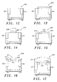
- FIGS. 12-19 are cross-sectional schematic diagrams of a method of fabricating a tunable antifuse element according to the present invention. More specifically, FIGS. 12-19 illustrate a method of fabricating a tunable antifuse element including a tunable gate oxide having a geometry as described in FIG. 10 . It should be understood that the method described and illustrated in FIGS. 12-19 could also be used to fabricate a tunable antifuse element similar to the tunable antifuse elements described with respect to FIGS. 1-5 , or having any gate oxide geometry such as those described in FIGS. 6-9 and 11 . In general, the tunable antifuse element of the present invention uses conventional DGO processes to create a tunable gate oxide comprised of a plurality of dielectric thicknesses and varying geometries.
- FIGS. 12-19 illustrate the fabrication steps of a tunable antifuse element 904 .
- the process steps are offered by way of example as one method for reduction to practice of conceived embodiments. Other methods are anticipated as would be obvious to one skilled in the art, and the scope of this description is not intended to be limited to this general process description.
- a substrate 101 is provided having a pwell 112 formed therein.
- Substrate material 101 may be a standard semiconductor substrate such-as bulk or epitaxial silicon substrate and is intended to encompass the relatively pure silicon materials typically used in the semiconductor industry, silicon-on-insulator, as well as silicon compound semiconductors, such as silicon germanium and the like. Metals and other conductive materials may be considered when forming metal-insulator-metal (MIM) capacitor.
- MIM metal-insulator-metal
- Pwell 112 is formed by ion implantation of boron or other means to a concentration of between ⁇ 1 ⁇ 10 14 /cm 3 and ⁇ 5 ⁇ 10 17 /cm 3 .
- shallow trench isolation (STI) 103 is next formed by conventional etch and refill methods. STI 103 provides separation between tunable antifuse element 904 and any devices proximate antifuse element 904 .
- a thick insulating layer 906 is formed over the entire substrate 101 .
- Thick insulating layer 906 is typically formed of silicon nitride, silicon oxide, a high K dielectric, or other similar insulating material.
- Thick insulating layer 906 is next patterned using a mask layer 908 as illustrated in FIG. 14 , such as a DGO mask, such that a portion of thick insulating layer 906 formed on an active area of tunable antifuse element 904 , similar to active area 106 of tunable antifuse element 102 ( FIG. 10 ) is etched way.
- mask layer 908 is removed.
- FIG. 15 illustrates the possible subtraction of a portion 909 of substrate 101 due to over-etch when substrate 101 undergoes undesirable silicon loss due to the etch step to remove thick insulating layer 906 .
- FIG. 16 illustrates a thin oxide layer 910 that is next grown over the active area of tunable antifuse element 904 .
- Layer of thin oxide 910 that is grown directly on substrate 101 in portions 909 will grow at a faster speed than layer of thin oxide 910 that is grown in an active area of tunable antifuse element 904 where growth is over thick oxide layer 906 .
- the resulting layers 910 formed in portions 909 will remain thinner than the combination layer grown in areas covered by thick oxide layer 906 .
- thin oxide layer 910 may be accomplished by using standard deposition techniques in which thin oxide layer 910 will grow on a surface of thick oxide layer 906 , or by using thermal oxidation techniques in which thin oxide layer 910 actually grows underneath layer 906 as illustrated in FIG. 16 .
- the resultant dual oxide layers in active area 106 of tunable antifuse element 904 serve as a stepped tunable gate oxide comprising a geometry similar to that described in FIG. 10 . More specifically, a single thin oxide layer 910 surrounds a central portion 911 , comprised of thick oxide layer 906 formed on top of thin oxide layer 910 .
- Gate oxide 110 has a stepped structure 912 defined by thin oxide layer 910 and thick oxide layer 906 as shown in FIG. 16 .
- a layer of polysilicon 914 is deposited on the surface of the device as illustrated in FIG. 17 .
- a mask layer 918 is next deposited providing for subsequent patterning and etching of polysilicon layer 914 and fabrication of gate 916 as illustrated in FIGS. 18 and 19 .
- the formation of well contacts 920 by implantation follows, as illustrated in FIG. 19 .
- tunable antifuse element 904 is fabricated in generally the same manner as a conventional antifuse element, except that additional photolithography and etch steps are performed during fabrication of tunable antifuse element 904 to provide for varying gate oxide thicknesses and geometries.
- the additional mask and wet etch step are actually part of standard CMOS process flow. Accordingly, the method described is most compatible with extant CMOS flows but other methods, such as an etchback, can also be used.
- FIG. 20 illustrates an antifuse array 950 , including a plurality of antifuse elements 952 , formed generally similar to tunable antifuse element 102 of FIGS. 1-3 .
- Antifuse elements 952 are capacitors and may optionally be combined with a series select transistor 954 to form a plurality of bit cells 956 .
- Antifuse array 950 is comprised of plurality of tunable antifuse elements 952 and a plurality of series select transistors 954 that in combination form plurality of bit cells 956 .
- a sector 958 indicated by the dashed line, is being programmed.
- bit cells 956 are arranged to form array 950 , the use of low PROGRAM and READ biases allows low voltage (LV) and dual gate oxide (DGO) transistors to be used as select transistors 954 , and provide increased array density.
- Antifuse elements 952 have a dielectric breakdown that is below that of logic and DGO transistors. This low breakdown voltage allows for a high-density array and produces low cost per bit.
- Array 950 can be programmed one row at a time without PROGRAM DISTURB in unselected rows. During programming, only one row and certain select transistor 954 gates are at non-zero biases. The bits to be programmed experience a bias close to the programming voltage (Vp). Select gates protect the bits that are not being programmed in the selected rows.
- FIG. 21 illustrates reading of antifuse array 950 without READ DISTURB in unselected rows.
- sector 958 indicated by the dashed line, is being read.
- READ bias polarity in antifuse elements 952 can be opposite to the PROGRAM bias polarity.
- Shorted bits connect their wordlines 960 and source lines 962 , resulting in current flow on their word lines 960 .
- Unprogrammed bit cells 956 do not experience significant conduction at these lower biases.
- the architecture of array 950 and operation allows reliability to be maintained over many READ cycles and allows for reverse polarity programming and readings, adding a degree of freedom to further optimize reliability.
- bit-count antifuse array in a cost-effective manner, allows for applications such as: (i) security applications; (ii) IC customization by customer; (iii) IC customization by manufacturer; (iv) IC identification and tracking; (v) “black-box” writes; (vi) more extensive and distributed trim; (vii) storage of very small programs; and (viii) field programmability.
- a tunable antifuse element comprising: a substrate material; an active area formed in a surface of the substrate material; a gate electrode having at least a portion positioned above the active area; and a tunable dielectric layer including a stepped structure, the tunable dielectric layer disposed between the gate electrode and the active area such that a voltage between the gate electrode and the active area creates a current path through the tunable dielectric layer and a rupture of the tunable dielectric layer in a rupture region.
- the tunable antifuse element is a capacitor.
- the substrate material is a semiconductor material.
- the active area comprises an electrically conductive doped region.
- the tunable dielectric layer is a tunable gate oxide layer.
- the tunable gate oxide layer is comprised of at least one thin oxide portion having a thickness T 1 and at least one thick oxide portion having a thickness T 2 , wherein T 1 is less than T 2 , the stepped structure defined by a thickness variation between the thin oxide portion and the thick oxide portion.
- the stepped structure includes a plurality of thick oxide portions and at least one thin oxide portion.
- the stepped structure includes a plurality of thin oxide portions and at least one thick oxide portion.
- the rupture region is located at a transition region between the at least one thick oxide portion and the at least one thin oxide portion.
- a method of fabricating a tunable antifuse element comprising: providing a substrate material; forming an active area in a surface of the substrate material; forming a gate electrode having at least a portion positioned above the active area; and forming a tunable dielectric layer including a stepped structure, the tunable dielectric layer disposed between the gate electrode and the active area such that a voltage between the gate electrode and the active area creates a current path through the tunable dielectric layer and a rupture of the tunable dielectric layer at a rupture region.
- the step of forming a tunable dielectric layer includes forming at least one thick oxide portion having a thickness T 2 and at least one thin oxide portion having a thickness T 1 , wherein T 1 is less than T 2 .
- the at least one thick oxide portion and the at least one thin oxide portion of the tunable gate oxide layer are formed using a dual gate oxide mask.
- the step of forming a tunable dielectric layer includes forming a first insulating layer over the substrate material, etching away a portion of the first insulating layer to expose a portion of the substrate material, and forming a second insulating layer, wherein a portion of the second insulating layer is formed as one of over or under the first insulating layer and a portion is formed over the exposed portion of the substrate material, thereby defining the stepped gate oxide structure.
- a tunable antifuse array comprising: a plurality of bit cells, each of the plurality of bit cells comprising at least one tunable antifuse element, wherein each of the at least one tunable antifuse elements is comprised of: a substrate material; an active area formed in a surface of the substrate material; a gate electrode having at least a portion positioned above the active area; and a tunable dielectric layer including a stepped structure, the tunable dielectric layer disposed between the gate electrode and the active area such that a voltage between the gate electrode and the active area creates a current path through the tunable dielectric layer and a rupture of the tunable dielectric layer in a rupture region.
- the tunable antifuse array further includes at least one select transistor.
- the at least one tunable antifuse element is a capacitor.
- the tunable dielectric layer is comprised of at least one thin oxide portion having a thickness T 1 and at least one thick oxide portion having a thickness T 2 , wherein T 1 is less than T 2, a stepped structure defined by a thickness variation between the thin oxide portion and the thick oxide portion.
- the stepped structure includes a plurality of thick oxide portions and at least one thin oxide portion.
- the stepped structure includes a plurality of thin oxide portions and at least one thick oxide portion. The rupture region is located at a transition region between the at least one thick oxide portion and the at least one thin oxide portion.
Landscapes
- Design And Manufacture Of Integrated Circuits (AREA)
- Semiconductor Memories (AREA)
- Semiconductor Integrated Circuits (AREA)
Abstract
Description
Claims (5)
Priority Applications (4)
| Application Number | Priority Date | Filing Date | Title |
|---|---|---|---|
| US11/169,962 US7528015B2 (en) | 2005-06-28 | 2005-06-28 | Tunable antifuse element and method of manufacture |
| PCT/US2006/022278 WO2007001782A2 (en) | 2005-06-28 | 2006-06-08 | Tunable antifuse element and method of manufacture |
| TW095121896A TWI399847B (en) | 2005-06-28 | 2006-06-19 | Tunable anti-fuse element and method of manufacturing same |
| US12/361,944 US7700996B2 (en) | 2005-06-28 | 2009-01-29 | Tunable antifuse elements |
Applications Claiming Priority (1)
| Application Number | Priority Date | Filing Date | Title |
|---|---|---|---|
| US11/169,962 US7528015B2 (en) | 2005-06-28 | 2005-06-28 | Tunable antifuse element and method of manufacture |
Related Child Applications (1)
| Application Number | Title | Priority Date | Filing Date |
|---|---|---|---|
| US12/361,944 Division US7700996B2 (en) | 2005-06-28 | 2009-01-29 | Tunable antifuse elements |
Publications (2)
| Publication Number | Publication Date |
|---|---|
| US20060292755A1 US20060292755A1 (en) | 2006-12-28 |
| US7528015B2 true US7528015B2 (en) | 2009-05-05 |
Family
ID=37568035
Family Applications (2)
| Application Number | Title | Priority Date | Filing Date |
|---|---|---|---|
| US11/169,962 Expired - Lifetime US7528015B2 (en) | 2005-06-28 | 2005-06-28 | Tunable antifuse element and method of manufacture |
| US12/361,944 Expired - Lifetime US7700996B2 (en) | 2005-06-28 | 2009-01-29 | Tunable antifuse elements |
Family Applications After (1)
| Application Number | Title | Priority Date | Filing Date |
|---|---|---|---|
| US12/361,944 Expired - Lifetime US7700996B2 (en) | 2005-06-28 | 2009-01-29 | Tunable antifuse elements |
Country Status (3)
| Country | Link |
|---|---|
| US (2) | US7528015B2 (en) |
| TW (1) | TWI399847B (en) |
| WO (1) | WO2007001782A2 (en) |
Families Citing this family (14)
| Publication number | Priority date | Publication date | Assignee | Title |
|---|---|---|---|---|
| JP4981661B2 (en) | 2004-05-06 | 2012-07-25 | サイデンス コーポレーション | Split channel antifuse array structure |
| US8767433B2 (en) | 2004-05-06 | 2014-07-01 | Sidense Corp. | Methods for testing unprogrammed OTP memory |
| US7755162B2 (en) | 2004-05-06 | 2010-07-13 | Sidense Corp. | Anti-fuse memory cell |
| US9123572B2 (en) | 2004-05-06 | 2015-09-01 | Sidense Corporation | Anti-fuse memory cell |
| US8735297B2 (en) | 2004-05-06 | 2014-05-27 | Sidense Corporation | Reverse optical proximity correction method |
| US7511982B2 (en) | 2004-05-06 | 2009-03-31 | Sidense Corp. | High speed OTP sensing scheme |
| US8159895B2 (en) | 2006-08-17 | 2012-04-17 | Broadcom Corporation | Method and system for split threshold voltage programmable bitcells |
| US7471540B2 (en) * | 2007-01-24 | 2008-12-30 | Kilopass Technology, Inc. | Non-volatile semiconductor memory based on enhanced gate oxide breakdown |
| US7892907B2 (en) * | 2008-10-31 | 2011-02-22 | Freescale Semiconductor, Inc. | CMOS latch-up immunity |
| CN105849861B (en) * | 2014-04-03 | 2018-08-10 | 新诺普系统公司 | Antifuse memory cell |
| US9202815B1 (en) * | 2014-06-20 | 2015-12-01 | Infineon Technologies Ag | Method for processing a carrier, a carrier, and a split gate field effect transistor structure |
| US10032783B2 (en) * | 2015-10-30 | 2018-07-24 | Globalfoundries Singapore Pte. Ltd. | Integrated circuits having an anti-fuse device and methods of forming the same |
| CA3005838C (en) | 2015-11-18 | 2022-06-07 | Corning Optical Communications LLC | System and method for monitoring strain in roadway optical cable |
| FR3091018B1 (en) | 2018-12-21 | 2023-01-20 | St Microelectronics Sa | microchip memory |
Citations (20)
| Publication number | Priority date | Publication date | Assignee | Title |
|---|---|---|---|---|
| US4016588A (en) * | 1974-12-27 | 1977-04-05 | Nippon Electric Company, Ltd. | Non-volatile semiconductor memory device |
| US4115914A (en) * | 1976-03-26 | 1978-09-26 | Hughes Aircraft Company | Electrically erasable non-volatile semiconductor memory |
| US4521796A (en) | 1980-12-11 | 1985-06-04 | General Instrument Corporation | Memory implant profile for improved channel shielding in electrically alterable read only memory semiconductor device |
| US4672409A (en) * | 1980-12-25 | 1987-06-09 | Fujitsu Limited | Nonvolatile semiconductor memory device |
| US5215934A (en) * | 1989-12-21 | 1993-06-01 | Tzeng Jyh Cherng J | Process for reducing program disturbance in eeprom arrays |
| US5352618A (en) * | 1993-07-30 | 1994-10-04 | Atmel Corporation | Method for forming thin tunneling windows in EEPROMs |
| US5475253A (en) | 1992-08-21 | 1995-12-12 | Xilinx, Inc. | Antifuse structure with increased breakdown at edges |
| US5780341A (en) * | 1996-12-06 | 1998-07-14 | Halo Lsi Design & Device Technology, Inc. | Low voltage EEPROM/NVRAM transistors and making method |
| US5915171A (en) | 1997-10-20 | 1999-06-22 | United Semiconductor Corp. | Process of fabricating an antifuse structure |
| US6096580A (en) | 1999-09-24 | 2000-08-01 | International Business Machines Corporation | Low programming voltage anti-fuse |
| US6130469A (en) | 1998-04-24 | 2000-10-10 | International Business Machines Corporation | Electrically alterable antifuse using FET |
| US6207588B1 (en) * | 1997-10-17 | 2001-03-27 | Samsung Electronics Co., Ltd. | Method for simultaneously forming thinner and thicker parts of a dual oxide layer having varying thicknesses |
| US6281558B1 (en) * | 1998-03-26 | 2001-08-28 | Mitsubishi Denki Kabushiki Kaisha | Semiconductor device and manufacturing method thereof |
| US6515344B1 (en) | 1999-10-28 | 2003-02-04 | Advanced Micro Devices, Inc. | Thin oxide anti-fuse |
| US6531410B2 (en) * | 2001-02-27 | 2003-03-11 | International Business Machines Corporation | Intrinsic dual gate oxide MOSFET using a damascene gate process |
| US20040156234A1 (en) * | 2002-04-26 | 2004-08-12 | Peng Jack Zezhong | High density semiconductor memory cell and memory array using a single transistor and having variable gate oxide breakdown |
| US6794726B2 (en) | 2002-04-17 | 2004-09-21 | International Business Machines Corporation | MOS antifuse with low post-program resistance |
| US20040238916A1 (en) | 2002-08-01 | 2004-12-02 | Trivedi Jigish D. | Edge intensive antifuse and method for making the same |
| US20050007855A1 (en) | 2003-06-28 | 2005-01-13 | Korea Advanced Institute Of Science And Technology | 3-Transistor OTP ROM using CMOS gate oxide antifuse |
| US7268387B2 (en) | 2001-05-31 | 2007-09-11 | Semiconductor Energy Laboratory Co., Ltd. | Semiconductor device and an electronic device |
Family Cites Families (2)
| Publication number | Priority date | Publication date | Assignee | Title |
|---|---|---|---|---|
| US5057451A (en) * | 1990-04-12 | 1991-10-15 | Actel Corporation | Method of forming an antifuse element with substantially reduced capacitance using the locos technique |
| US7126172B2 (en) * | 2004-10-12 | 2006-10-24 | Freescale Semiconductor, Inc. | Integration of multiple gate dielectrics by surface protection |
-
2005
- 2005-06-28 US US11/169,962 patent/US7528015B2/en not_active Expired - Lifetime
-
2006
- 2006-06-08 WO PCT/US2006/022278 patent/WO2007001782A2/en not_active Ceased
- 2006-06-19 TW TW095121896A patent/TWI399847B/en not_active IP Right Cessation
-
2009
- 2009-01-29 US US12/361,944 patent/US7700996B2/en not_active Expired - Lifetime
Patent Citations (23)
| Publication number | Priority date | Publication date | Assignee | Title |
|---|---|---|---|---|
| US4016588A (en) * | 1974-12-27 | 1977-04-05 | Nippon Electric Company, Ltd. | Non-volatile semiconductor memory device |
| US4115914A (en) * | 1976-03-26 | 1978-09-26 | Hughes Aircraft Company | Electrically erasable non-volatile semiconductor memory |
| US4521796A (en) | 1980-12-11 | 1985-06-04 | General Instrument Corporation | Memory implant profile for improved channel shielding in electrically alterable read only memory semiconductor device |
| US4672409A (en) * | 1980-12-25 | 1987-06-09 | Fujitsu Limited | Nonvolatile semiconductor memory device |
| US5215934A (en) * | 1989-12-21 | 1993-06-01 | Tzeng Jyh Cherng J | Process for reducing program disturbance in eeprom arrays |
| US5475253A (en) | 1992-08-21 | 1995-12-12 | Xilinx, Inc. | Antifuse structure with increased breakdown at edges |
| US5502000A (en) | 1992-08-21 | 1996-03-26 | Xilinx, Inc. | Method of forming a antifuse structure with increased breakdown at edges |
| US5352618A (en) * | 1993-07-30 | 1994-10-04 | Atmel Corporation | Method for forming thin tunneling windows in EEPROMs |
| US5780341A (en) * | 1996-12-06 | 1998-07-14 | Halo Lsi Design & Device Technology, Inc. | Low voltage EEPROM/NVRAM transistors and making method |
| US6207588B1 (en) * | 1997-10-17 | 2001-03-27 | Samsung Electronics Co., Ltd. | Method for simultaneously forming thinner and thicker parts of a dual oxide layer having varying thicknesses |
| US5915171A (en) | 1997-10-20 | 1999-06-22 | United Semiconductor Corp. | Process of fabricating an antifuse structure |
| US6281558B1 (en) * | 1998-03-26 | 2001-08-28 | Mitsubishi Denki Kabushiki Kaisha | Semiconductor device and manufacturing method thereof |
| US6130469A (en) | 1998-04-24 | 2000-10-10 | International Business Machines Corporation | Electrically alterable antifuse using FET |
| US6096580A (en) | 1999-09-24 | 2000-08-01 | International Business Machines Corporation | Low programming voltage anti-fuse |
| US6515344B1 (en) | 1999-10-28 | 2003-02-04 | Advanced Micro Devices, Inc. | Thin oxide anti-fuse |
| US6531410B2 (en) * | 2001-02-27 | 2003-03-11 | International Business Machines Corporation | Intrinsic dual gate oxide MOSFET using a damascene gate process |
| US20030109090A1 (en) | 2001-02-27 | 2003-06-12 | International Business Machines Corporation | Intrinsic dual gate oxide mosfet using a damascene gate process |
| US7268387B2 (en) | 2001-05-31 | 2007-09-11 | Semiconductor Energy Laboratory Co., Ltd. | Semiconductor device and an electronic device |
| US6794726B2 (en) | 2002-04-17 | 2004-09-21 | International Business Machines Corporation | MOS antifuse with low post-program resistance |
| US20040156234A1 (en) * | 2002-04-26 | 2004-08-12 | Peng Jack Zezhong | High density semiconductor memory cell and memory array using a single transistor and having variable gate oxide breakdown |
| US20040238916A1 (en) | 2002-08-01 | 2004-12-02 | Trivedi Jigish D. | Edge intensive antifuse and method for making the same |
| US20040238917A1 (en) | 2002-08-01 | 2004-12-02 | Trivedi Jigish D. | Edge intensive antifuse and method for making the same |
| US20050007855A1 (en) | 2003-06-28 | 2005-01-13 | Korea Advanced Institute Of Science And Technology | 3-Transistor OTP ROM using CMOS gate oxide antifuse |
Non-Patent Citations (4)
| Title |
|---|
| Candelier et al., "One Time Programmable Drift Antifuse Cell Reliability," IEEE 38th Annual International Reliability Physics Symposium, San Jose, CA 2000, pp. 169-173. |
| Henley, W.B. et al., "Effects of Iron Contamination on Thin Oxide Breakdowns and Reliability Characteristics", Proc. Intl. Reliability Physics Symposium, pp. 22-27, 1993. |
| International Search Report and Written Opinion for correlating PCT Patent Application No. PCT/US06/22278 dated Jul. 3, 2008. |
| Li, F. et al, "Evaluation of SiO2 Antifuse in a 3D-OTP Memory", IEEE Trans. Dev. and Mat. Reliability, vol. 4, No. 3, pp. 416-421, Sep. 2004. |
Also Published As
| Publication number | Publication date |
|---|---|
| US20060292755A1 (en) | 2006-12-28 |
| WO2007001782A2 (en) | 2007-01-04 |
| US20090127587A1 (en) | 2009-05-21 |
| WO2007001782A3 (en) | 2009-04-16 |
| TW200717781A (en) | 2007-05-01 |
| TWI399847B (en) | 2013-06-21 |
| US7700996B2 (en) | 2010-04-20 |
Similar Documents
| Publication | Publication Date | Title |
|---|---|---|
| US7700996B2 (en) | Tunable antifuse elements | |
| US7834417B2 (en) | Antifuse elements | |
| US7511352B2 (en) | Rail Schottky device and method of making | |
| US8299570B2 (en) | Efuse containing sige stack | |
| KR101287015B1 (en) | High―density nonvolatile memory array fabricated at low temperature comprising semiconductor diodes | |
| US4922319A (en) | Semiconductor programmable memory device | |
| US8722518B2 (en) | Methods for protecting patterned features during trench etch | |
| KR101873281B1 (en) | Anti-fuse memory cell | |
| TWI518849B (en) | Electronic device including non-volatile memory structure with anti-fuse assembly and method of forming same | |
| US8163640B2 (en) | Metal gate compatible electrical fuse | |
| US6335228B1 (en) | Method for making an anti-fuse | |
| US7279772B2 (en) | Edge intensive antifuse and method for making the same | |
| US20100181643A1 (en) | Efuse with partial sige layer and design structure therefor | |
| US7256471B2 (en) | Antifuse element and electrically redundant antifuse array for controlled rupture location | |
| KR20070010077A (en) | Isolated Channel Antifuse Array Architecture | |
| US9478555B2 (en) | Method for processing a carrier, a carrier, and a split gate field effect transistor structure | |
| KR100890018B1 (en) | Isolation of memory cells in cross point arrays | |
| US20230020696A1 (en) | Memory device and formation method thereof | |
| TWI878794B (en) | Semiconductor device having fuse component | |
| US20050124097A1 (en) | Integrated circuit with two phase fuse material and method of using and making same | |
| US6277724B1 (en) | Method for forming an array of sidewall-contacted antifuses having diffused bit lines | |
| JP2010245102A (en) | Semiconductor device and manufacturing method thereof | |
| CN117377314A (en) | Semiconductor components |
Legal Events
| Date | Code | Title | Description |
|---|---|---|---|
| AS | Assignment |
Owner name: FREESCALE SEMICONDUCTOR, INC., TEXAS Free format text: ASSIGNMENT OF ASSIGNORS INTEREST;ASSIGNORS:PARRIS, PATRICE M.;CHEN, WEIZE;MCKENNA, JOHN M.;AND OTHERS;REEL/FRAME:016750/0174 Effective date: 20050624 |
|
| AS | Assignment |
Owner name: CITIBANK, N.A. AS COLLATERAL AGENT, NEW YORK Free format text: SECURITY AGREEMENT;ASSIGNORS:FREESCALE SEMICONDUCTOR, INC.;FREESCALE ACQUISITION CORPORATION;FREESCALE ACQUISITION HOLDINGS CORP.;AND OTHERS;REEL/FRAME:018855/0129 Effective date: 20061201 Owner name: CITIBANK, N.A. AS COLLATERAL AGENT,NEW YORK Free format text: SECURITY AGREEMENT;ASSIGNORS:FREESCALE SEMICONDUCTOR, INC.;FREESCALE ACQUISITION CORPORATION;FREESCALE ACQUISITION HOLDINGS CORP.;AND OTHERS;REEL/FRAME:018855/0129 Effective date: 20061201 |
|
| FEPP | Fee payment procedure |
Free format text: PAYOR NUMBER ASSIGNED (ORIGINAL EVENT CODE: ASPN); ENTITY STATUS OF PATENT OWNER: LARGE ENTITY |
|
| STCF | Information on status: patent grant |
Free format text: PATENTED CASE |
|
| AS | Assignment |
Owner name: CITIBANK, N.A., NEW YORK Free format text: SECURITY AGREEMENT;ASSIGNOR:FREESCALE SEMICONDUCTOR, INC.;REEL/FRAME:023273/0099 Effective date: 20090804 Owner name: CITIBANK, N.A.,NEW YORK Free format text: SECURITY AGREEMENT;ASSIGNOR:FREESCALE SEMICONDUCTOR, INC.;REEL/FRAME:023273/0099 Effective date: 20090804 |
|
| AS | Assignment |
Owner name: CITIBANK, N.A., AS COLLATERAL AGENT,NEW YORK Free format text: SECURITY AGREEMENT;ASSIGNOR:FREESCALE SEMICONDUCTOR, INC.;REEL/FRAME:024397/0001 Effective date: 20100413 Owner name: CITIBANK, N.A., AS COLLATERAL AGENT, NEW YORK Free format text: SECURITY AGREEMENT;ASSIGNOR:FREESCALE SEMICONDUCTOR, INC.;REEL/FRAME:024397/0001 Effective date: 20100413 |
|
| FPAY | Fee payment |
Year of fee payment: 4 |
|
| AS | Assignment |
Owner name: CITIBANK, N.A., AS NOTES COLLATERAL AGENT, NEW YORK Free format text: SECURITY AGREEMENT;ASSIGNOR:FREESCALE SEMICONDUCTOR, INC.;REEL/FRAME:030633/0424 Effective date: 20130521 Owner name: CITIBANK, N.A., AS NOTES COLLATERAL AGENT, NEW YOR Free format text: SECURITY AGREEMENT;ASSIGNOR:FREESCALE SEMICONDUCTOR, INC.;REEL/FRAME:030633/0424 Effective date: 20130521 |
|
| AS | Assignment |
Owner name: CITIBANK, N.A., AS NOTES COLLATERAL AGENT, NEW YORK Free format text: SECURITY AGREEMENT;ASSIGNOR:FREESCALE SEMICONDUCTOR, INC.;REEL/FRAME:031591/0266 Effective date: 20131101 Owner name: CITIBANK, N.A., AS NOTES COLLATERAL AGENT, NEW YOR Free format text: SECURITY AGREEMENT;ASSIGNOR:FREESCALE SEMICONDUCTOR, INC.;REEL/FRAME:031591/0266 Effective date: 20131101 |
|
| AS | Assignment |
Owner name: FREESCALE SEMICONDUCTOR, INC., TEXAS Free format text: PATENT RELEASE;ASSIGNOR:CITIBANK, N.A., AS COLLATERAL AGENT;REEL/FRAME:037354/0823 Effective date: 20151207 Owner name: FREESCALE SEMICONDUCTOR, INC., TEXAS Free format text: PATENT RELEASE;ASSIGNOR:CITIBANK, N.A., AS COLLATERAL AGENT;REEL/FRAME:037354/0225 Effective date: 20151207 Owner name: FREESCALE SEMICONDUCTOR, INC., TEXAS Free format text: PATENT RELEASE;ASSIGNOR:CITIBANK, N.A., AS COLLATERAL AGENT;REEL/FRAME:037356/0553 Effective date: 20151207 Owner name: FREESCALE SEMICONDUCTOR, INC., TEXAS Free format text: PATENT RELEASE;ASSIGNOR:CITIBANK, N.A., AS COLLATERAL AGENT;REEL/FRAME:037356/0143 Effective date: 20151207 |
|
| AS | Assignment |
Owner name: MORGAN STANLEY SENIOR FUNDING, INC., MARYLAND Free format text: ASSIGNMENT AND ASSUMPTION OF SECURITY INTEREST IN PATENTS;ASSIGNOR:CITIBANK, N.A.;REEL/FRAME:037486/0517 Effective date: 20151207 |
|
| AS | Assignment |
Owner name: MORGAN STANLEY SENIOR FUNDING, INC., MARYLAND Free format text: ASSIGNMENT AND ASSUMPTION OF SECURITY INTEREST IN PATENTS;ASSIGNOR:CITIBANK, N.A.;REEL/FRAME:037518/0292 Effective date: 20151207 |
|
| AS | Assignment |
Owner name: MORGAN STANLEY SENIOR FUNDING, INC., MARYLAND Free format text: SUPPLEMENT TO THE SECURITY AGREEMENT;ASSIGNOR:FREESCALE SEMICONDUCTOR, INC.;REEL/FRAME:039138/0001 Effective date: 20160525 |
|
| FPAY | Fee payment |
Year of fee payment: 8 |
|
| AS | Assignment |
Owner name: NXP, B.V., F/K/A FREESCALE SEMICONDUCTOR, INC., NETHERLANDS Free format text: RELEASE BY SECURED PARTY;ASSIGNOR:MORGAN STANLEY SENIOR FUNDING, INC.;REEL/FRAME:040925/0001 Effective date: 20160912 Owner name: NXP, B.V., F/K/A FREESCALE SEMICONDUCTOR, INC., NE Free format text: RELEASE BY SECURED PARTY;ASSIGNOR:MORGAN STANLEY SENIOR FUNDING, INC.;REEL/FRAME:040925/0001 Effective date: 20160912 |
|
| AS | Assignment |
Owner name: NXP B.V., NETHERLANDS Free format text: RELEASE BY SECURED PARTY;ASSIGNOR:MORGAN STANLEY SENIOR FUNDING, INC.;REEL/FRAME:040928/0001 Effective date: 20160622 |
|
| AS | Assignment |
Owner name: NXP USA, INC., TEXAS Free format text: CHANGE OF NAME;ASSIGNOR:FREESCALE SEMICONDUCTOR INC.;REEL/FRAME:040652/0180 Effective date: 20161107 |
|
| AS | Assignment |
Owner name: NXP USA, INC., TEXAS Free format text: CORRECTIVE ASSIGNMENT TO CORRECT THE NATURE OF CONVEYANCE LISTED CHANGE OF NAME SHOULD BE MERGER AND CHANGE PREVIOUSLY RECORDED AT REEL: 040652 FRAME: 0180. ASSIGNOR(S) HEREBY CONFIRMS THE MERGER AND CHANGE OF NAME;ASSIGNOR:FREESCALE SEMICONDUCTOR INC.;REEL/FRAME:041354/0148 Effective date: 20161107 |
|
| AS | Assignment |
Owner name: MORGAN STANLEY SENIOR FUNDING, INC., MARYLAND Free format text: CORRECTIVE ASSIGNMENT TO CORRECT THE REMOVE PATENTS 8108266 AND 8062324 AND REPLACE THEM WITH 6108266 AND 8060324 PREVIOUSLY RECORDED ON REEL 037518 FRAME 0292. ASSIGNOR(S) HEREBY CONFIRMS THE ASSIGNMENT AND ASSUMPTION OF SECURITY INTEREST IN PATENTS;ASSIGNOR:CITIBANK, N.A.;REEL/FRAME:041703/0536 Effective date: 20151207 |
|
| AS | Assignment |
Owner name: SHENZHEN XINGUODU TECHNOLOGY CO., LTD., CHINA Free format text: CORRECTIVE ASSIGNMENT TO CORRECT THE TO CORRECT THE APPLICATION NO. FROM 13,883,290 TO 13,833,290 PREVIOUSLY RECORDED ON REEL 041703 FRAME 0536. ASSIGNOR(S) HEREBY CONFIRMS THE THE ASSIGNMENT AND ASSUMPTION OF SECURITYINTEREST IN PATENTS.;ASSIGNOR:MORGAN STANLEY SENIOR FUNDING, INC.;REEL/FRAME:048734/0001 Effective date: 20190217 Owner name: SHENZHEN XINGUODU TECHNOLOGY CO., LTD., CHINA Free format text: CORRECTIVE ASSIGNMENT TO CORRECT THE TO CORRECT THE APPLICATION NO. FROM 13,883,290 TO 13,833,290 PREVIOUSLY RECORDED ON REEL 041703 FRAME 0536. ASSIGNOR(S) HEREBY CONFIRMS THE THE ASSIGNMENT AND ASSUMPTION OF SECURITY INTEREST IN PATENTS.;ASSIGNOR:MORGAN STANLEY SENIOR FUNDING, INC.;REEL/FRAME:048734/0001 Effective date: 20190217 |
|
| AS | Assignment |
Owner name: NXP B.V., NETHERLANDS Free format text: RELEASE BY SECURED PARTY;ASSIGNOR:MORGAN STANLEY SENIOR FUNDING, INC.;REEL/FRAME:050744/0097 Effective date: 20190903 |
|
| AS | Assignment |
Owner name: MORGAN STANLEY SENIOR FUNDING, INC., MARYLAND Free format text: CORRECTIVE ASSIGNMENT TO CORRECT THE REMOVE APPLICATION11759915 AND REPLACE IT WITH APPLICATION 11759935 PREVIOUSLY RECORDED ON REEL 037486 FRAME 0517. ASSIGNOR(S) HEREBY CONFIRMS THE ASSIGNMENT AND ASSUMPTION OF SECURITYINTEREST IN PATENTS;ASSIGNOR:CITIBANK, N.A.;REEL/FRAME:053547/0421 Effective date: 20151207 Owner name: MORGAN STANLEY SENIOR FUNDING, INC., MARYLAND Free format text: CORRECTIVE ASSIGNMENT TO CORRECT THE REMOVE APPLICATION 11759915 AND REPLACE IT WITH APPLICATION 11759935 PREVIOUSLY RECORDED ON REEL 037486 FRAME 0517. ASSIGNOR(S) HEREBY CONFIRMS THE ASSIGNMENT AND ASSUMPTION OF SECURITY INTEREST IN PATENTS;ASSIGNOR:CITIBANK, N.A.;REEL/FRAME:053547/0421 Effective date: 20151207 |
|
| AS | Assignment |
Owner name: NXP B.V., NETHERLANDS Free format text: CORRECTIVE ASSIGNMENT TO CORRECT THE REMOVEAPPLICATION 11759915 AND REPLACE IT WITH APPLICATION11759935 PREVIOUSLY RECORDED ON REEL 040928 FRAME 0001. ASSIGNOR(S) HEREBY CONFIRMS THE RELEASE OF SECURITYINTEREST;ASSIGNOR:MORGAN STANLEY SENIOR FUNDING, INC.;REEL/FRAME:052915/0001 Effective date: 20160622 Owner name: NXP B.V., NETHERLANDS Free format text: CORRECTIVE ASSIGNMENT TO CORRECT THE REMOVE APPLICATION 11759915 AND REPLACE IT WITH APPLICATION 11759935 PREVIOUSLY RECORDED ON REEL 040928 FRAME 0001. ASSIGNOR(S) HEREBY CONFIRMS THE RELEASE OF SECURITY INTEREST;ASSIGNOR:MORGAN STANLEY SENIOR FUNDING, INC.;REEL/FRAME:052915/0001 Effective date: 20160622 |
|
| AS | Assignment |
Owner name: NXP, B.V. F/K/A FREESCALE SEMICONDUCTOR, INC., NETHERLANDS Free format text: CORRECTIVE ASSIGNMENT TO CORRECT THE REMOVEAPPLICATION 11759915 AND REPLACE IT WITH APPLICATION11759935 PREVIOUSLY RECORDED ON REEL 040925 FRAME 0001. ASSIGNOR(S) HEREBY CONFIRMS THE RELEASE OF SECURITYINTEREST;ASSIGNOR:MORGAN STANLEY SENIOR FUNDING, INC.;REEL/FRAME:052917/0001 Effective date: 20160912 Owner name: NXP, B.V. F/K/A FREESCALE SEMICONDUCTOR, INC., NETHERLANDS Free format text: CORRECTIVE ASSIGNMENT TO CORRECT THE REMOVE APPLICATION 11759915 AND REPLACE IT WITH APPLICATION 11759935 PREVIOUSLY RECORDED ON REEL 040925 FRAME 0001. ASSIGNOR(S) HEREBY CONFIRMS THE RELEASE OF SECURITY INTEREST;ASSIGNOR:MORGAN STANLEY SENIOR FUNDING, INC.;REEL/FRAME:052917/0001 Effective date: 20160912 |
|
| MAFP | Maintenance fee payment |
Free format text: PAYMENT OF MAINTENANCE FEE, 12TH YEAR, LARGE ENTITY (ORIGINAL EVENT CODE: M1553); ENTITY STATUS OF PATENT OWNER: LARGE ENTITY Year of fee payment: 12 |