EP0807953A1 - Inductively coupled RF plasma reactor having an overhead solenoidal antenna - Google Patents
Inductively coupled RF plasma reactor having an overhead solenoidal antenna Download PDFInfo
- Publication number
- EP0807953A1 EP0807953A1 EP97303244A EP97303244A EP0807953A1 EP 0807953 A1 EP0807953 A1 EP 0807953A1 EP 97303244 A EP97303244 A EP 97303244A EP 97303244 A EP97303244 A EP 97303244A EP 0807953 A1 EP0807953 A1 EP 0807953A1
- Authority
- EP
- European Patent Office
- Prior art keywords
- reactor
- antenna
- ceiling
- center
- workpiece
- Prior art date
- Legal status (The legal status is an assumption and is not a legal conclusion. Google has not performed a legal analysis and makes no representation as to the accuracy of the status listed.)
- Withdrawn
Links
Images


Classifications
-
- H—ELECTRICITY
- H01—ELECTRIC ELEMENTS
- H01L—SEMICONDUCTOR DEVICES NOT COVERED BY CLASS H10
- H01L21/00—Processes or apparatus adapted for the manufacture or treatment of semiconductor or solid state devices or of parts thereof
- H01L21/02—Manufacture or treatment of semiconductor devices or of parts thereof
- H01L21/04—Manufacture or treatment of semiconductor devices or of parts thereof the devices having potential barriers, e.g. a PN junction, depletion layer or carrier concentration layer
- H01L21/18—Manufacture or treatment of semiconductor devices or of parts thereof the devices having potential barriers, e.g. a PN junction, depletion layer or carrier concentration layer the devices having semiconductor bodies comprising elements of Group IV of the Periodic Table or AIIIBV compounds with or without impurities, e.g. doping materials
- H01L21/30—Treatment of semiconductor bodies using processes or apparatus not provided for in groups H01L21/20 - H01L21/26
- H01L21/302—Treatment of semiconductor bodies using processes or apparatus not provided for in groups H01L21/20 - H01L21/26 to change their surface-physical characteristics or shape, e.g. etching, polishing, cutting
- H01L21/306—Chemical or electrical treatment, e.g. electrolytic etching
- H01L21/3065—Plasma etching; Reactive-ion etching
-
- H—ELECTRICITY
- H01—ELECTRIC ELEMENTS
- H01J—ELECTRIC DISCHARGE TUBES OR DISCHARGE LAMPS
- H01J37/00—Discharge tubes with provision for introducing objects or material to be exposed to the discharge, e.g. for the purpose of examination or processing thereof
- H01J37/32—Gas-filled discharge tubes
- H01J37/32431—Constructional details of the reactor
- H01J37/32458—Vessel
-
- B—PERFORMING OPERATIONS; TRANSPORTING
- B01—PHYSICAL OR CHEMICAL PROCESSES OR APPARATUS IN GENERAL
- B01D—SEPARATION
- B01D53/00—Separation of gases or vapours; Recovering vapours of volatile solvents from gases; Chemical or biological purification of waste gases, e.g. engine exhaust gases, smoke, fumes, flue gases, aerosols
- B01D53/22—Separation of gases or vapours; Recovering vapours of volatile solvents from gases; Chemical or biological purification of waste gases, e.g. engine exhaust gases, smoke, fumes, flue gases, aerosols by diffusion
- B01D53/225—Multiple stage diffusion
- B01D53/226—Multiple stage diffusion in serial connexion
-
- B—PERFORMING OPERATIONS; TRANSPORTING
- B01—PHYSICAL OR CHEMICAL PROCESSES OR APPARATUS IN GENERAL
- B01D—SEPARATION
- B01D53/00—Separation of gases or vapours; Recovering vapours of volatile solvents from gases; Chemical or biological purification of waste gases, e.g. engine exhaust gases, smoke, fumes, flue gases, aerosols
- B01D53/26—Drying gases or vapours
- B01D53/268—Drying gases or vapours by diffusion
-
- C—CHEMISTRY; METALLURGY
- C23—COATING METALLIC MATERIAL; COATING MATERIAL WITH METALLIC MATERIAL; CHEMICAL SURFACE TREATMENT; DIFFUSION TREATMENT OF METALLIC MATERIAL; COATING BY VACUUM EVAPORATION, BY SPUTTERING, BY ION IMPLANTATION OR BY CHEMICAL VAPOUR DEPOSITION, IN GENERAL; INHIBITING CORROSION OF METALLIC MATERIAL OR INCRUSTATION IN GENERAL
- C23C—COATING METALLIC MATERIAL; COATING MATERIAL WITH METALLIC MATERIAL; SURFACE TREATMENT OF METALLIC MATERIAL BY DIFFUSION INTO THE SURFACE, BY CHEMICAL CONVERSION OR SUBSTITUTION; COATING BY VACUUM EVAPORATION, BY SPUTTERING, BY ION IMPLANTATION OR BY CHEMICAL VAPOUR DEPOSITION, IN GENERAL
- C23C16/00—Chemical coating by decomposition of gaseous compounds, without leaving reaction products of surface material in the coating, i.e. chemical vapour deposition [CVD] processes
- C23C16/44—Chemical coating by decomposition of gaseous compounds, without leaving reaction products of surface material in the coating, i.e. chemical vapour deposition [CVD] processes characterised by the method of coating
- C23C16/50—Chemical coating by decomposition of gaseous compounds, without leaving reaction products of surface material in the coating, i.e. chemical vapour deposition [CVD] processes characterised by the method of coating using electric discharges
- C23C16/517—Chemical coating by decomposition of gaseous compounds, without leaving reaction products of surface material in the coating, i.e. chemical vapour deposition [CVD] processes characterised by the method of coating using electric discharges using a combination of discharges covered by two or more of groups C23C16/503 - C23C16/515
-
- H—ELECTRICITY
- H01—ELECTRIC ELEMENTS
- H01J—ELECTRIC DISCHARGE TUBES OR DISCHARGE LAMPS
- H01J37/00—Discharge tubes with provision for introducing objects or material to be exposed to the discharge, e.g. for the purpose of examination or processing thereof
- H01J37/32—Gas-filled discharge tubes
- H01J37/32009—Arrangements for generation of plasma specially adapted for examination or treatment of objects, e.g. plasma sources
- H01J37/32082—Radio frequency generated discharge
- H01J37/321—Radio frequency generated discharge the radio frequency energy being inductively coupled to the plasma
-
- H—ELECTRICITY
- H01—ELECTRIC ELEMENTS
- H01J—ELECTRIC DISCHARGE TUBES OR DISCHARGE LAMPS
- H01J37/00—Discharge tubes with provision for introducing objects or material to be exposed to the discharge, e.g. for the purpose of examination or processing thereof
- H01J37/32—Gas-filled discharge tubes
- H01J37/32009—Arrangements for generation of plasma specially adapted for examination or treatment of objects, e.g. plasma sources
- H01J37/32082—Radio frequency generated discharge
- H01J37/32137—Radio frequency generated discharge controlling of the discharge by modulation of energy
- H01J37/32146—Amplitude modulation, includes pulsing
-
- H—ELECTRICITY
- H01—ELECTRIC ELEMENTS
- H01J—ELECTRIC DISCHARGE TUBES OR DISCHARGE LAMPS
- H01J37/00—Discharge tubes with provision for introducing objects or material to be exposed to the discharge, e.g. for the purpose of examination or processing thereof
- H01J37/32—Gas-filled discharge tubes
- H01J37/32009—Arrangements for generation of plasma specially adapted for examination or treatment of objects, e.g. plasma sources
- H01J37/32082—Radio frequency generated discharge
- H01J37/32137—Radio frequency generated discharge controlling of the discharge by modulation of energy
- H01J37/32155—Frequency modulation
- H01J37/32165—Plural frequencies
-
- H—ELECTRICITY
- H01—ELECTRIC ELEMENTS
- H01J—ELECTRIC DISCHARGE TUBES OR DISCHARGE LAMPS
- H01J37/00—Discharge tubes with provision for introducing objects or material to be exposed to the discharge, e.g. for the purpose of examination or processing thereof
- H01J37/32—Gas-filled discharge tubes
- H01J37/32431—Constructional details of the reactor
- H01J37/32458—Vessel
- H01J37/32467—Material
-
- H—ELECTRICITY
- H01—ELECTRIC ELEMENTS
- H01J—ELECTRIC DISCHARGE TUBES OR DISCHARGE LAMPS
- H01J37/00—Discharge tubes with provision for introducing objects or material to be exposed to the discharge, e.g. for the purpose of examination or processing thereof
- H01J37/32—Gas-filled discharge tubes
- H01J37/32431—Constructional details of the reactor
- H01J37/32458—Vessel
- H01J37/32522—Temperature
-
- H—ELECTRICITY
- H01—ELECTRIC ELEMENTS
- H01J—ELECTRIC DISCHARGE TUBES OR DISCHARGE LAMPS
- H01J37/00—Discharge tubes with provision for introducing objects or material to be exposed to the discharge, e.g. for the purpose of examination or processing thereof
- H01J37/32—Gas-filled discharge tubes
- H01J37/32431—Constructional details of the reactor
- H01J37/3266—Magnetic control means
- H01J37/32688—Multi-cusp fields
-
- H—ELECTRICITY
- H01—ELECTRIC ELEMENTS
- H01J—ELECTRIC DISCHARGE TUBES OR DISCHARGE LAMPS
- H01J37/00—Discharge tubes with provision for introducing objects or material to be exposed to the discharge, e.g. for the purpose of examination or processing thereof
- H01J37/32—Gas-filled discharge tubes
- H01J37/32431—Constructional details of the reactor
- H01J37/32697—Electrostatic control
- H01J37/32706—Polarising the substrate
-
- H—ELECTRICITY
- H01—ELECTRIC ELEMENTS
- H01J—ELECTRIC DISCHARGE TUBES OR DISCHARGE LAMPS
- H01J37/00—Discharge tubes with provision for introducing objects or material to be exposed to the discharge, e.g. for the purpose of examination or processing thereof
- H01J37/32—Gas-filled discharge tubes
- H01J37/32431—Constructional details of the reactor
- H01J37/32798—Further details of plasma apparatus not provided for in groups H01J37/3244 - H01J37/32788; special provisions for cleaning or maintenance of the apparatus
- H01J37/32853—Hygiene
- H01J37/32871—Means for trapping or directing unwanted particles
-
- H—ELECTRICITY
- H01—ELECTRIC ELEMENTS
- H01L—SEMICONDUCTOR DEVICES NOT COVERED BY CLASS H10
- H01L21/00—Processes or apparatus adapted for the manufacture or treatment of semiconductor or solid state devices or of parts thereof
- H01L21/02—Manufacture or treatment of semiconductor devices or of parts thereof
- H01L21/04—Manufacture or treatment of semiconductor devices or of parts thereof the devices having potential barriers, e.g. a PN junction, depletion layer or carrier concentration layer
- H01L21/18—Manufacture or treatment of semiconductor devices or of parts thereof the devices having potential barriers, e.g. a PN junction, depletion layer or carrier concentration layer the devices having semiconductor bodies comprising elements of Group IV of the Periodic Table or AIIIBV compounds with or without impurities, e.g. doping materials
- H01L21/30—Treatment of semiconductor bodies using processes or apparatus not provided for in groups H01L21/20 - H01L21/26
- H01L21/31—Treatment of semiconductor bodies using processes or apparatus not provided for in groups H01L21/20 - H01L21/26 to form insulating layers thereon, e.g. for masking or by using photolithographic techniques; After treatment of these layers; Selection of materials for these layers
- H01L21/3105—After-treatment
- H01L21/311—Etching the insulating layers by chemical or physical means
- H01L21/31105—Etching inorganic layers
- H01L21/31111—Etching inorganic layers by chemical means
- H01L21/31116—Etching inorganic layers by chemical means by dry-etching
-
- H—ELECTRICITY
- H01—ELECTRIC ELEMENTS
- H01L—SEMICONDUCTOR DEVICES NOT COVERED BY CLASS H10
- H01L21/00—Processes or apparatus adapted for the manufacture or treatment of semiconductor or solid state devices or of parts thereof
- H01L21/67—Apparatus specially adapted for handling semiconductor or electric solid state devices during manufacture or treatment thereof; Apparatus specially adapted for handling wafers during manufacture or treatment of semiconductor or electric solid state devices or components ; Apparatus not specifically provided for elsewhere
- H01L21/683—Apparatus specially adapted for handling semiconductor or electric solid state devices during manufacture or treatment thereof; Apparatus specially adapted for handling wafers during manufacture or treatment of semiconductor or electric solid state devices or components ; Apparatus not specifically provided for elsewhere for supporting or gripping
- H01L21/6831—Apparatus specially adapted for handling semiconductor or electric solid state devices during manufacture or treatment thereof; Apparatus specially adapted for handling wafers during manufacture or treatment of semiconductor or electric solid state devices or components ; Apparatus not specifically provided for elsewhere for supporting or gripping using electrostatic chucks
-
- H—ELECTRICITY
- H01—ELECTRIC ELEMENTS
- H01F—MAGNETS; INDUCTANCES; TRANSFORMERS; SELECTION OF MATERIALS FOR THEIR MAGNETIC PROPERTIES
- H01F29/00—Variable transformers or inductances not covered by group H01F21/00
- H01F29/14—Variable transformers or inductances not covered by group H01F21/00 with variable magnetic bias
- H01F2029/143—Variable transformers or inductances not covered by group H01F21/00 with variable magnetic bias with control winding for generating magnetic bias
-
- H—ELECTRICITY
- H01—ELECTRIC ELEMENTS
- H01J—ELECTRIC DISCHARGE TUBES OR DISCHARGE LAMPS
- H01J2237/00—Discharge tubes exposing object to beam, e.g. for analysis treatment, etching, imaging
- H01J2237/32—Processing objects by plasma generation
- H01J2237/33—Processing objects by plasma generation characterised by the type of processing
- H01J2237/334—Etching
- H01J2237/3343—Problems associated with etching
- H01J2237/3345—Problems associated with etching anisotropy
-
- H—ELECTRICITY
- H01—ELECTRIC ELEMENTS
- H01J—ELECTRIC DISCHARGE TUBES OR DISCHARGE LAMPS
- H01J2237/00—Discharge tubes exposing object to beam, e.g. for analysis treatment, etching, imaging
- H01J2237/32—Processing objects by plasma generation
- H01J2237/33—Processing objects by plasma generation characterised by the type of processing
- H01J2237/334—Etching
- H01J2237/3343—Problems associated with etching
- H01J2237/3346—Selectivity
Definitions
- the invention is related to inductively coupled RF plasma reactors of the type having a reactor chamber ceiling overlying a workpiece being processed and an inductive coil antenna adjacent the ceiling.
- Inductively coupled RF plasma reactors are employed to perform a variety of processes on workpieces such as semiconductor wafers.
- one type of inductively coupled RF plasma reactor has a reactor chamber 10 including a ceiling 12 and a cylindrical side wall 14.
- a pedestal 16 supports the workpiece 18, such as a semiconductor wafer, so that the workpiece generally lies in a workpiece support plane, and a bias RF power generator is coupled to the pedestal 16.
- a generally planar coil antenna 20 overlies the ceiling 12 and is coupled to a plasma source RF power generator 22.
- etch selectivity refers to the ratio of etch rates of two different materials exposed to etching in the reactor.
- etch selectivity refers to the ratio of etch rates of two different materials exposed to etching in the reactor.
- Polymer precursor gases e.g., fluorocarbon or fluorohydrocarbon gases
- Polymer precursor gases tend to polymerize strongly on non-oxygen-containing surfaces (such as silicon or photoresist), particularly at higher chamber pressures, and only weakly on oxygen-containing surfaces (such as silicon dioxide), so that the non-oxygen-containing surfaces are relatively well-protected from etching while oxygen-containing surfaces (such as silicon dioxide) are relatively unprotected and are etched.
- non-oxygen-containing surfaces such as silicon or photoresist
- oxygen-containing surfaces such as silicon dioxide
- Such a polymerization process enhances the oxide-to-silicon etch selectivity better at higher chamber pressures because the polymerization rate is higher at higher pressures such as 100 mT.
- the electron-to-neutral species elastic collision mean free path length which is inversely proportional to chamber pressure, determines the extent to which electrons can avoid recombination with other gas particles and diffuse through the plasma to produce a more uniform electron and ion distribution in the chamber.
- electrons are not generated uniformly throughout the chamber (due, for example, to a non-uniform inductive antenna pattern) and electron diffusion through the plasma compensates for this and provides greater electron and plasma ion spatial density distribution uniformity.
- Electrode spatial density distribution across the wafer surface directly affects plasma ion spatial density distribution because plasma ions are produced by collisions of process gas particles with energetic electrons.
- Increasing chamber pressure suppresses electron diffusion in the plasma, thereby reducing (degrading) plasma ion spatial density distribution uniformity.
- the inductive antenna 20 due to its circular symmetry, has an antenna pattern (i.e., a spatial distribution of the magnitude of the induced electric field) with a null or local minimum along the antenna axis of symmetry so that very few if any electrons are produced over the wafer center.
- antenna pattern i.e., a spatial distribution of the magnitude of the induced electric field
- null or local minimum along the antenna axis of symmetry
- a related problem is that the overall plasma density is greater near the ceiling 12 (where the density of hot electrons is greatest) than at the workpiece 18, and falls off more rapidly away from the ceiling 12 as chamber pressure is increased.
- the electron mean free path in an argon plasma with a mean electron temperature of 5eV at a chamber pressure of 1 mT is on the order of 10 cm, at 10 mT it is 1.0 cm and at 100 mT it is 0.1 cm.
- a high pressure regime is one in which the mean free path length is about 1/10 or more of the ceiling-to-workpiece gap.
- the inductive field skin depth corresponds to the depth through the plasma --measured downward from the ceiling 12-- within which the inductive field of the antenna 20 is nearly completely absorbed.
- FIG. 2 illustrates how skin depth in an argon plasma increases with chamber pressure above a threshold pressure or about 0.003 mT (below which the skin depth is virtually constant over pressure).
- FIG. 2 also illustrates in the dashed-line curve how electron-to-neutral elastic collision mean free path length decreases linearly with increasing pressure.
- the skin depth function graphed in FIG. 2 assumes a source frequency of 2 MHz and an argon plasma density of 5 ⁇ 10 17 electrons/m 3 .
- the graph of FIG. 2 was derived using a collision cross-section for an electron temperature of 5eV in argon. (It should be noted that with a molecular gas such as C 2 F 6 instead of argon, the collision cross-section is greater so that the skin depth is greater at a given pressure and the entire curve of FIG.
- the chamber pressure is such that the inductive field is absorbed within a small fraction --e.g., 1/10th-- of the ceiling-to-workpiece gap adjacent the ceiling 12 (corresponding to a pressure of 1 mT for a 5 cm gap in the example of FIG. 2), then electron diffusion --throughout the remaining 3/10ths of the gap-- produces a more uniform plasma ion distribution at the workpiece surface.
- a measure of a high skin depth regime is that in which the skin depth is at about 1/10 or more of the source-to-workpiece gap length.
- any antenna pattern null or local minimum extends to the surface of the workpiece 18, effectively preventing electron diffusion from compensating for the effects of the antenna pattern null on the processing of the workpiece.
- Such problems can arise, for example, when the ceiling-to-workpiece spacing is decreased in order to increase overall plasma density at the workpiece surface.
- a related problem with a small ceiling-to-workpiece spacing and a high chamber pressure is that electrons are lost not only to recombination with particles in the processing gas but are also lost to recombination by collisions with the surface of the ceiling 12 and the workpiece 18, so that it is even more difficult for electrons generated in other regions to diffuse into the region adjacent the workpiece center.
- plasma ion density at the wafer can be enhanced by reducing the gap between the axially symmetrical antenna/ceiling 20, 12 and the workpiece 13. But if the gap is reduced so much that the inductive field skin depth becomes a substantial fracticn ( ⁇ 10%) of the gap, then ion density at the workpiece center falls off significantly relative to the edge due to the antenna pattern's center null. However, for a smaller fraction of skin depth over gap and sufficient electron diffusion (characteristic of a low chamber pressure), electrons produced far from the workpiece center may diffuse into the center region before being lost to gas phase recombination or surface recombination, thereby compensating for the antenna pattern's center null.
- the plasma ion density decreases at the wafer center and ultimately, at very short wafer-to-antenna distances, becomes a center null giving rise to an unacceptable process non-uniformity.
- the etch rate at the wafer center may be so much less than elsewhere that it becomes impossible to perform a complete etch across the entire wafer surface without over-etching near the wafer periphery.
- the problem is to find a way to decrease the wafer-to-antenna distance without incurring a concomitant penalty in process non-uniformity.
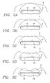
- FIG. 3A illustrates the plasma ion density as a function of radius from the center of the workpiece 18 for a workpiece-to-ceiling height of 4 inches (10 cm), the curve labelled A being the ion density produced by the outer coil antenna 24 and the curve labelled B being the ion density produced by the inner coil antenna 20.
- the total resulting plasma ion density is the sum of these two curves but is not depicted in the drawing for the sake of simplicity.
- FIG. 3A shows that at a height of 4 inches (10 cm), the outer coil antenna 24 produces a uniform plasma ion density distribution, the inner coil antenna 20 not being required.
- FIG. 3B corresponds to FIG.
- FIG. 3A for a reduced workpiece-to-ceiling height of 3 inches (7.5 cm), and shows that a dip in plasma ion density produced by the outer coil antenna 24 is compensated by the center-dominated ion density produced by the inner ccil antenna 20.
- FIG. 3C corresponds to FIG. 3A for a further reduced workpiece-to-ceiling height of 2.5 inches (6.25 cm), and shows that the compensation by the inner coil 20 for the center dip in the plasma ion density produced by the outer coil 24 remains fairly effective as the workpiece-to-ceiling height is further reduced, although a slight dip in the total resulting plasma ion density near the center would begin to appear belcw this height.
- FIG. 3C corresponds to FIG. 3A for a further reduced workpiece-to-ceiling height of 2.5 inches (6.25 cm), and shows that the compensation by the inner coil 20 for the center dip in the plasma ion density produced by the outer coil 24 remains fairly effective as the workpiece-to-ceiling height is further reduced,
- FIGS. 3A-3E show is that even the use of inner and outer coil antennas to solve the problem of the null in plasma ion density near the workpiece center may lose effectiveness as the workpiece-to-ceiling height is reduced below certain values. Thus, the wafer-to-ceiling height cannot be reduced below a factor of the skin depth without sacrificing process uniformity. On the other hand, unless the wafer-to-ceiling height can be so reduced, plasma density and process performance is limited. Accordingly, there is a need for a way to reduce the workpiece-co-ceiling height without sacrificing process uniformity.
- the invention is embodied in an inductively coupled RF plasma reactor including a reactor chamber enclosure defining a plasma reactor chamber and a support for holding a workpiece inside the chamber, a non-planar inductive antenna adjacent the reactor chamber enclosure, the non-planar inductive antenna including inductive elements spatially distributed in a non-planar manner relative to a plane of the workpiece, and a plasma source RF power supply coupled to the non-planar inductive antenna.
- the non-planar distribution of the antenna's inductive elements is such that the inductive elements are spatially distributed approximately in respective planes intersecting the axis of symmetry.
- the inductive antenna may be either asymmetrical or symmetrical, the inductive antenna preferably includes a symmetrical solenoid winding such as a vertical stack of inductive windings.
- the invention provides a means for adjusting such processing parameters as plasma ion density distribution across the surface of the workpiece. More specifically, the invention compensates for a null in an RF inductive pattern of the antenna, which is typically near an axis of symmetry of the antenna.
- the windings are at a minimum radial distance from the axis of symmetry of the antenna so as to concentrate the induction field over the workpiece center for optimum process uniformity at small workpiece-to-antenna distances.
- the windings are at a radial distance from the axis of symmetry which is a substantial fraction of a radius of the chamber.
- This radial distance is selected to be an optimum value which provides the greatest uniformity in plasma ion density under particular conditions which may include sources of process non-uniformities in addition to the antenna pattern center null.
- the determination of the optimum radial distance can be carried out by the skilled worker by trial and error steps of placing the solenoid winding at different radial locations and employing conventional techniques to determine the radial profile of the plasma ion density at each step.
- the reactor may further include a second inductive antenna adjacent the reactor enclosure at an outer radial location relative to the solenoid winding and, preferably, a second plasma source RF power supply coupled to the second inductive antenna for independent adjustment of RF power applied to the inner and outer antennas.
- the second inductive antenna is a second non-planar inductive antenna.
- the second non-planar inductive antenna is a solenoid winding.
- the reactor solenoid winding may be a doubly wound solenoid winding, which may consist of either a pair of concentric single solenoid windings or a vertical stack of pairs of windings. Likewise, if there is a second radially outward solenoid winding, then the second solenoid winding may be a doubly wound solenoid winding.
- the vertical stack of conductive windings may have a right cylindrical shape, an upright conical shape or an inverted conical shape or a non-symmetrical shape.
- a planar coil conductor may extend radially outwardly from a bottom winding of the vertical stack of conductive windings.
- the invention is not confined to any particular non-planar configuration or shape, and any suitable shape can be employed which performs the function of providing the requisite concentration of the RF induction field near the center axis to compensate for the antenna pattern center null.
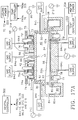
- FIG. 1 is a cut-away side view of an inductively coupled plasma reactor of the type employed in a co-pending U.S. patent application referred to above employing generally planar coil antennas.
- FIG. 2 is a log-log scale graph of induction field skin depth in a plasma in cm (solid line) and of electron-to-neutral elastic collision mean free path length (dashed line) as functions of pressure in torr (horizontal axis).
- FIG. 3A is a graph of plasma ion density as a function of radial position relative to the workpiece center in the reactor of FIG. 1 for a workpiece-to-ceiling height of 4 inches, the curves labelled A and B corresponding to plasma ion densities produced by outer and inner coil antennas respectively.
- FIG. 3B is a graph of plasma ion density as a function of radial position relative to the workpiece center in the reactor of FIG. 1 for a workpiece-to-ceiling height of 3 inches, the curves labelled A and B corresponding to plasma ion densities produced by outer and inner coil antennas respectively.
- FIG. 3C is a graph of plasma ion density as a function of radial position relative to the workpiece center in the reactor of FIG. 1 for a workpiece-to-ceiling height of 2.5 inches, the curves labelled A and B corresponding to plasma ion densities produced by outer and inner coil antennas respectively.
- FIG. 3D is a graph of plasma ion density as a function of radial position relative to the workpiece center in the reactor of FIG. 1 for a workpiece-to-ceiling height of 1.25 inches, the curves labelled A and B corresponding to plasma ion densities produced by outer and inner coil antennas respectively.
- FIG. 3E is a graph of plasma ion density as a function of radial position relative to the workpiece center in the reactor of FIG. 1 for a workpiece-to-ceiling height of 0.8 inches, the curves labelled A and B corresponding to plasma ion densities produced by outer and inner coil antennas respectively.
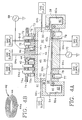
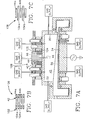
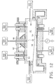
- FIG. 4A is a cut-away side view of a plasma reactor in accordance with an alternative embodiment of the invention employing a single three-dimensional center non-planar solenoid winding.
- FIG. 4B is an enlarged view of a portion of the reactor of FIG. 4A illustrating a preferred way of winding the solenoidal winding.
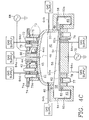
- FIG. 4C is a cut-away side view of a plasma reactor corresponding to FIG. 4A but having a dome-shaped ceiling.
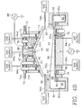
- FIG. 4D is a cut-away side view of a plasma reactor corresponding to FIG. 4A but having a conical ceiling.
- FIG. 4E is a cut-away side view of a plasma reactor corresponding to FIG. 4D but having a truncated conical ceiling.
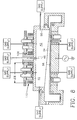
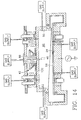
- FIG. 5 is a cut-away side view of a plasma reactor in accordance with the preferred embodiment of the invention employing inner and outer vertical solenoid windings.
- FIG. 6 is a cut-away side view of a plasma reactor in accordance with a second alternative embodiment of the invention corresponding to FIG. 5 in which the outer winding is flat.
- FIG. 7A is a cut-away side view of a plasma reactor in accordance with a third alternative embodiment of the invention corresponding to FIG. 4A in which the center solenoid winding consists of plural upright cylindrical windings.
- FIG. 73 is a detailed view of a first implementation of the embodiment of FIG. 7A.
- FIG. 7C is a detailed view of a second implementation of the embodiment of FIG. 7A.
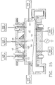
- FIG. 8 is a cut-away side view of a plasma reactor in accordance with a fourth alternative embodiment of the invention corresponding to FIG. 5 in which both the inner and outer windings consist of plural upright cylindrical windings.
- FIG. 9 is a cut-away side view of a plasma reactor in accordance with a fifth alternative embodiment of the invention corresponding to FIG. 5 in which the inner winding consists of plural upright cylindrical windings and the outer winding consists of a single upright cylindrical winding.
- FIG. 10 is a cut-away side view of a plasma reactor in accordance with a sixth alternative embodiment of the invention in which a single solenoid winding is placed at an optimum radial position for maximum plasma ion density uniformity.
- FIG. 11 is a cut-away side view of a plasma reactor in accordance with a seventh alternative embodiment of the invention corresponding to FIG. 4A in which the solenoid winding is an inverted conical shape.
- FIG. 12 is a cut-away side view of a plasma reactor in accordance with an eighth alternative embodiment of the invention corresponding to FIG. 4A in which the solenoid winding is an upright conical shape.
- FIG. 13 is a cut-away side view of a plasma reactor in accordance with a ninth alternative embodiment of the invention corresponding to FIG. 4A in which the solenoid winding consists of an inner upright cylindrical portion and an outer flat portion.
- FIG. 14 is a cut-away side view of a plasma reactor in accordance with a tenth alternative embodiment of the invention corresponding to FIG. 10 in which the solenoid winding includes both an inverted conical portion and a flat portion.
- FIG. 15 is a cut-away side view of a plasma reactor in accordance with an eleventh alternative embodiment of the invention corresponding to FIG. 12 in which the solenoid winding includes both an upright conical portion and a flat portion.
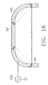
- FIG. 16 illustrates another embodiment of the invention employing a combination of planar, conical and dome-shaped ceiling elements.
- FIG. 17A illustrates an alternative embodiment of the invention employing a separately biased silicon side wall and ceiling and employing electrical heaters.
- FIG. 17B illustrates an alternative embodiment of the invention employing separately biased inner and outer silicon ceiling portions and employing electrical heaters.
- the invention In a plasma reactor having a small antenna-to-workpiece gap, in order to minimize the decrease in plasma ion density near the center region of the workpiece corresponding to the inductive antenna pattern center null, it is an object of the invention to increase the magnitude of the induced electric field at the center region.
- the invention accomplishes this by concentrating the turns of an inductive coil overlying the ceiling near the axis of symmetry of the antenna and maximizing the rate of change (at the RF source frequency) of magnetic flux linkage between the antenna and the plasma in that center region.
- a solenoidal coil around the symmetry axis simultaneously concentrates its inductive coil turns near the axis and maximizes the rate of change of magnetic flux linkage between the antenna and the plasma in the center region adjacent the workpiece. This is because the number of turns is large and the coil radius is small, as required for strong flux linkage and close mutual coupling to the plasma in the center region.
- a solenoid-like antenna is one which has plural inductive elements distributed in a non-planar manner relative to a plane of the workpiece or workpiece support surface or overlying chamber ceiling, or spaced at different distances transversely to the workpiece support plane (defined by a workpiece supporting pedestal within the chamber) or spaced at different distances transversely to an overlying chamber ceiling.
- an inductive element is a current-carrying element mutually coupled with the plasma in the chamber and/or with other inductive elements of the antenna.
- a preferred embodiment of the invention includes dual solenoidal coil antennas with one solenoid near the center and another one at an outer peripheral radius.
- the two solenoids may be driven at different RF frequencies or at the same frequency, in which case they are preferably phase-locked and more preferably phase-locked in such a manner that their fields constructively interact.
- the greatest practical displacement between the inner and outer solenoid is preferred because it provides the most versatile control of etch rate at the workpiece center relative to etch rate at the workpiece periphery.
- FIG. 4A illustrates a single solenoid embodiment (not the preferred embodiment) of an inductively coupled RF plasma reactor having a short workpiece-to-ceiling gap, meaning that the skin depth of the induction field is on the order of the gap length.
- a skin depth which is on the order of the gap length is that which is within a factor of ten of (i.e., between about one tenth and about ten times) the gap length.
- FIG. 5 illustrates a dual solenoid embodiment of an inductively coupled RF plasma reactor, and is the preferred embodiment of the invention. Except for the dual solenoid feature, the reactor structure of the embodiments of FIGS. 4A and 5 is nearly the same, and will now be described with reference to FIG. 4A.
- the reactor includes a cylindrical chamber 40 similar to that of FIG. 1, except that the reactor of FIG. 4A has a non-planar coil antenna 42 whose windings 44 are closely concentrated in non-planar fashion near the antenna symmetry axis 46. While in the illustrated embodiment the windings 44 are symmetrical and their symmetry axis 46 coincides with the center axis of the chamber, the invention may be carried out differently. For example, the windings may not be symmetrical and/or their axis of symmetry may not coincide. However, in the case of a symmetrical antenna, the antenna has a radiation pattern null near its symmetry axis 46 coinciding with the center of the chamber or the workpiece center.
- the RF power applied to the non-planar coil antenna 42 produces greater induction [d/dt] [N•I] at the wafer center --at the antenna symmetry axis 46-- (relative to the peripheral regions) and therefore produces greater plasma ion density in that region, so that the resulting plasma ion density is more nearly uniform despite the small workpiece-to-ceiling height.
- the invention provides a way for reducing the ceiling height for enhanced plasma process performance without sacrificing process uniformity.
- FIG. 4B best shows a preferred implementation of the windings employed in the embodiments of FIGS. 4A and 5.
- the windings 44 be at least nearly parallel to the plane of the workpiece 56, they preferably are not wound in the usual manner of a helix but, instead, are preferably wound so that each individual turn is parallel to the (horizontal) plane of the workpiece 56 except at a step or transition 44a between turns (from one horizontal plane to the next).
- the cylindrical chamber 40 consists of a cylindrical side wall 50 and a circular ceiling 52 integrally formed with the side wall 50 so that the side wall 50 and ceiling 52 constitute a single piece of material, such as silicon.
- the invention may be carried out with the side wall 50 and ceiling 52 formed as separate pieces, as will be described later in this specification.
- the circular ceiling 52 may be of any suitable cross-sectional shape such as planar (FIG. 4A), dome (FIG. 4C), conical (FIG. 4D), truncated conical (FIG. 4E), cylindrical or any combination of such shapes or curve of rotation. Such a combination will be discussed later in this specification.
- the vertical pitch of the solenoid 42 exceeds the vertical pitch of the ceiling 52, even for ceilings defining 3-dimensional surfaces such as dome, conical, truncated conical and so forth.
- the purpose for this, at least in the preferred embodiment, is to concentrate the induction of the antenna near the antenna symmetry axis, as discussed previously in this specification.
- a solenoid having a pitch exceeding that of the ceiling 52 is referred to herein as a non-conformal solenoid, meaning that, in general, its shape does not conform with the shape of the ceiling, and more specifically that its vertical pitch exceeds the vertical pitch of the ceiling.
- a 2-dimensional or flat ceiling has a vertical pitch of zero, while a 3-dimensional ceiling has a non-zero vertical pitch.
- a pedestal 54 at the bottom of the chamber 40 supports a planar workpiece 56 in a workpiece support plane during processing.
- the workpiece 56 is typically a semiconductor wafer and the workpiece support plane is generally the plane of the wafer or workpiece 56.
- the chamber 40 is evacuated by a pump (not shown in the drawing) through an annular passage 58 to a pumping annulus 60 surrounding the lower portion of the chamber 40.
- the interior of the pumping annulus may be lined with a replaceable metal liner 60a.
- the annular passage 58 is defined by the bottom edge 50a of the cylindrical side wall 50 and a planar ring 62 surrounding the pedestal 54.
- Process gas is furnished into the chamber 40 through any one or all of a variety of gas feeds.
- a center gas feed 64a can extend downwardly through the center of the ceiling 52 toward the center of the workpiece 56 (or the center of the workpiece support plane).
- plural radial gas feeds 64b which can be controlled independently of the center gas feed 64a, extend radially inwardly from the side wall 50 toward the workpiece periphery (or toward the workpiece support plane periphery), or base axial gas feeds 64c extend upwardly from near the pedestal 54 toward the workpiece periphery, or ceiling axial gas feeds 64d can extend downwardly from the ceiling 52 toward the workpiece periphery.
- Etch rates at the workpiece center and periphery can be adjusted independently relative to one another to achieve a more radially uniform etch rate distribution across the workpiece by controlling the process gas flow rates toward the workpiece center and periphery through, respectively, the center gas feed 64a and any one of the outer gas feeds 64b-d.
- This feature of the invention can be carried out with the center gas feed 64a and only one of the peripheral gas feeds 64b-d.
- the solenoidal coil antenna 42 is wound around a housing 66 surrounding the center gas feed 64a.
- a plasma source RF power supply 68 is connected across the coil antenna 42 and a bias RF power supply 70 is connected to the pedestal 54.
- Coolant passages 74a contain a coolant of a known variety having a high thermal conductivity but a low electrical conductivity, to avoid electrically loading down the antenna or solenoid 42.
- the cold plate 74 provides constant cooling of the ceiling 52 while the maximum power of the radiant heaters 72 is selected so as to be able to overwhelm, if necessary, the cooling by the cold plate 74, facilitating responsive and stable temperature control of the ceiling 52.
- the large ceiling area irradiated by the heaters 72 provides greater uniformity and efficiency of temperature control. (It should be noted that radiant heating is not necessarily required in carrying out the invention, and the skilled worker may choose to employ an electric heating element instead, as will be described later in this specification.) If the ceiling 52 is silicon, as disclosed in co-pending U.S. application Serial No. 08/597,577 filed February 2, 1996 by Kenneth S.
- a polymer precursor and etchant precursor process gas e.g., a fluorocarbon gas
- the etchant e.g., fluorine
- the rate of polymer deposition across the entire ceiling 52 and/or the rate at which the ceiling 52 furnishes a fluorine etchant scavenger material (silicon) into the plasma is better controlled by increasing the contact area of the ceiling 52 with the temperature control heater 72.
- the solenoid antenna 42 increases the available contact area on the ceiling 52 because the solenoid windings 44 are concentrated at the center axis of the ceiling 52.
- a highly thermally conductive torus 75 formed of a ceramic such as aluminum nitride, aluminum oxide or silicon nitride or of a non-ceramic like silicon either lightly doped or undoped
- a highly thermally conductive torus 75 formed of a ceramic such as aluminum nitride, aluminum oxide or silicon nitride or of a non-ceramic like silicon either lightly doped or undoped
- One feature of the torus 75 is that it displaces the cold plate 74 well-above the top of the solenoid 42. This feature substantially mitigates or nearly eliminates the reduction in inductive coupling between the solenoid 42 and the plasma which would otherwise result from a close proximity of the conductive plane of the cold place 74 to the solenoid 42.
- the distance between the cold plate 74 and the top winding of the solenoid 42 be at least a substantial fraction (e.g., one half) of the total height of the solenoid 42.
- Plural axial holes 75a extending through the torus 75 are spaced along two concentric circles and hold the plural radiant heaters or lamps 72 and permit them to directly irradiate the ceiling 52.
- the hole interior surface may be lined with a reflective (e.g., aluminum) layer.
- the center gas feed 64a of FIG. 4A may be replaced by a radiant heater 72 (as shown in FIG. 5), depending upon the particular reactor design and process conditions.
- the ceiling temperature is sensed by a sensor such as a thermocouple 76 extending through one of the holes 75a not occupied by a lamp heater 72.
- a sensor such as a thermocouple 76 extending through one of the holes 75a not occupied by a lamp heater 72.
- a highly thermally conductive elastomer 73 such as silicone rubber impregnated with boron nitride is placed between the ceramic torus 75 and the copper cold plate 74 and between the ceramic torus 75 and the silicon ceiling 52.
- the chamber 40 may be an all-semiconductor chamber, in which case the ceiling 52 and the side wall 50 are both a semiconductor material such as silicon.
- controlling the temperature of, and RF bias power applied to, either the ceiling 52 or the wall 50 regulates the extent to which it furnishes fluorine scavenger precursor material (silicon) into the plasma or, alternatively, the extent to which it is coated with polymer.
- the material of the ceiling 52 is nct limited to silicon but may be, in the alternative, silicon carbide, silicon dioxide (quartz), silicon nitride or a ceramic.
- the chamber wall or ceiling 50, 52 need not be used as the source of a fluorine scavenger material.
- a disposable silicon member can be placed inside the chamber 40 and maintained at a sufficiently high temperature to prevent polymer condensation thereon and permit silicon material to be removed therefrom into the plasma as fluorine scavenging material.
- the wall 50 and ceiling 52 need not necessarily be silicon, or if they are silicon they may be maintained at a temperature (and/or RF bias) near or below the polymer condensation temperature (and/or a polymer condensation RF bias threshold) so that they are coated with polymer from the plasma so as to be protected from being consumed. While the disposable silicon member may take any appropriate form, in the embodiment of FIG.
- the disposable silicon member is an annular ring 62 surrounding the pedestal 54.
- the annular ring 62 is high purity silicon and may be doped to alter its electrical or optical properties.
- plural radiant (e.g., tungsten halogen lamp) heaters 77 arranged in a circle under the annular ring 62 heat the silicon ring 62 through a quartz window 78.
- the heaters 77 are controlled in accordance with the measured temperature of the silicon ring 62 sensed by a temperature sensor 79 which may be a remote sensor such as an optical pyrometer or a fluoro-optical probe.
- the sensor 79 may extend partially intc a very deep hole 62a in the ring 62, the deepness and narrowness of the hole tending at least partially to mask temperature-dependent variations in thermal emissivity of the silicon ring 62, so that it behaves more like a gray-body radiator for more reliable temperature measurement.
- an advantage of an all-semiconductor chamber is that the plasma is free of contact with contaminant producing materials such as metal, fcr example.
- plasma confinement magnets 80, 82 adjacent the annular opening 58 prevent or reduce plasma flow into the pumping annulus 60.
- any polymer precursor and/or active species succeeds in entering the pumping annulus 60, any resulting polymer or contaminant deposits on the replaceable interior liner 60a may be prevented from reentering the plasma chamber 40 by maintaining the liner 60a at a temperature significantly below the polymer condensation temperature, for example, as disclosed in the referenced co-pending application.
- a wafer slit valve 84 through the exterior wall of the pumping annulus 60 accommodates wafer ingress and egress.
- the annular opening 58 between the chamber 40 and pumping annulus 60 is larger adjacent the wafer slit valve 84 and smallest on the opposite side by virtue of a slant of the bottom edge 50a of the cylindrical side wall 50 so as to make the chamber pressure distribution more symmetrical with a non-symmetrical pump port location.
- a second outer vertical stack or solenoid 90 of windings 92 at an outer location is displaced by a radial distance 6R from the inner vertical stack of solenoidal windings 44.
- confinement of the inner solenoidal antenna 42 to the center and the outer solenoidal antenna 90 to the periphery leaves a large portion of the top surface of the ceiling 52 available for direct contact with the temperature control apparatus 72, 74, 75, as in FIG. 4A.
- the wafer-to-ceiling gap is 3 in (7.5 cm)
- the mean diameter of the inner solenoid was 3.75 in (9.3 cm) while the mean diameter of the outer solenoid was 11.75 in (29.3 cm) using 3/16 in diameter hollow copper tubing covered with a 0.03 thick teflon insulation layer, each solenoid consisting of four turns and being 1 in (2.54 cm) high.
- the outer stack or solenoid 90 is energized by a second independently controllable plasma source RF power supply 96.
- etch performance at the workpiece center may be adjusted relative to etch performance at the edge by adjusting the RF power applied to the inner solenoid 42 relative to that applied to the outer solenoid 90 and adjusting the gas flow rate through the center gas feed 64a relative to the flow rate through the outer gas feeds 64b-d.
- the present invention solves or at least ameliorates the problem of a center null or dip in the inductance field as described above, there may be other plasma processing non-uniformity problems, and these can be compensated in the versatile embodiment of FIG. 5 by adjusting the relative RF power levels applied to the inner and outer antennas 42, 90.
- the respective RF power supplies 68, 96 for the inner and outer solenoids 42, 90 may be replaced by a common power supply 97a and a power splitter 97b which permits the user to change the relative apportionment of power between the inner and outer solenoids 42, 90 while preserving a fixed phase relationship between the fields of the inner and outer solenoids 42, 90.
- the two solenoids 42, 90 receive RF power at the same frequency.
- the two independent power supplies 68, 96 may be powered at different RF frequencies, in which case it is preferable to install RF filters at the output cf each RF power supply 68, 96 to avoid off-frequency feedback from coupling between the two solenoids.
- the frequency difference should be sufficient to time-average out coupling between the two solenoids and, furthermore, should exceed the rejection bandwidth of the RF filters.
- Another option is to make each frequency independently resonantly matched to the respective solenoid, and each frequency may be varied to follow changes in the plasma impedance (thereby maintaining resonance) in lieu of conventional impedance matching techniques.
- the RF frequency applied to the antenna is made to follow the resonant frequency of the antenna as loaded by the impedance of the plasma in the chamber.
- the frequency ranges of the two solenoids should be mutually exclusive.
- the two solenoids are driven at the same RF frequency and in this case it is preferable that the phase relationship between the two be such as to cause constructive interaction or superposition of the fields of the two solenoids.
- this requirement will be met by a zero phase angle between the signals applied to the two solenoids if they are both wound in the same sense. Otherwise, if they are oppositely wound, the phase angle is preferably 180°.
- coupling between the inner and outer solenoids can be minimized or eliminated by having a relatively large space between the inner and outer solenoids 42, 90, as will be discussed below in this specification.
- the range attainable by such adjustments is increased by increasing the radius of the outer solenoid 90 to increase the spacing between the inner and outer solenoids 42, 90, so that the effects of the two solenoids 42, 90 are more confined to the workpiece center and edge, respectively.
- the radius cf the inner solenoid 42 should be no greater than about half the workpiece radius and preferably no more than about a third thereof.
- the minimum radius of the inner solenoid 42 is affected in part by the diameter of the conductor forming the solenoid 42 and in part by the need to provide a finite non-zero circumference for an arcuate --e.g., circular-- current path to produce inductance.
- the radius of the outer coil 90 should be at least equal to the workpiece radius and preferably 1.5 or more times the workpiece radius. With such a configuration, the respective center and edge effects of the inner and outer solenoids 42, 90 are so pronounced that by increasing power to the inner solenoid the chamber pressure can be raised into the hundreds of mT while providing a uniform plasma, and by increasing power to the outer solenoid 90 the chamber pressure can be reduced to on the order of 0.01 mT while providing a uniform plasma. Another advantage of such a large radius of the outer solenoid 90 is that it minimizes coupling between the inner and outer solenoids 42, 90.
- FIG. 5 indicates in dashed line that a third solenoid 94 may be added as an option, which is desireable for a very large chamber diameter.
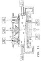
- FIG. 6 illustrates a variation of the embodiment of FIG. 5 in which the outer solenoid 90 is replaced by a planar winding 100.
- FIG. 7A illustrates a variation of the embodiment of FIG. 4A in which the center solenoidal winding includes not only the vertical stack 42 of windings 44 but in addition a second vertical stack 102 of windings 104 closely adjacent to the first stack 42 so that the two stacks constitute a double-wound solenoid 106.
- the doubly wound solenoid 106 may consist of two independently wcund single solenoids 42, 102, the inner solenoid 42 consisting of the windings 44a, 44b, and so forth and the outer solenoid 102 consisting of the winding 104a, 104b and so forth.
- FIG. 7A illustrates a variation of the embodiment of FIG. 4A in which the center solenoidal winding includes not only the vertical stack 42 of windings 44 but in addition a second vertical stack 102 of windings 104 closely adjacent to the first stack 42 so that the two stacks constitute a double-wound solenoid 106.
- the doubly wound solenoid 106 may consist of
- the doubly wound solenoid 106 may consist of vertically stacked pairs of at least nearly co-planar windings.
- each pair of nearly co-planar windings e.g., the pair 44a, 104a or the pair 44b, 104b
- each pair of nearly co-planar windings may be formed by helically winding a single conductor.
- the term "doubly wound” used herein refers to winding of the type shown in either FIG. 7B or 7C.
- the solenoid winding may not be merely doubly wound but may be triply wound or more and in general it can consists of plural windings at each plane along the axis of symmetry.
- Such multiple-wound solenoids may be employed in either one cr both the inner and outer solenoids 42, 90 of the dual-solenoid embodiment of FIG. 5.
- FIG. 8 illustrates a variation of the embodiment of FIG. 7A in which an outer doubly wound solenoid 110 concentric with the inner doubly wound solenoid 106 is placed at a radial distance ⁇ R from the inner solenoid 106.
- FIG. 9 illustrates a variation of the embodiment of FIG. 8 in which the outer doubly wound solenoid 110 is replaced by an ordinary outer solenoid 112 corresponding to the outer solenoid employed in the embodiment of FIG. 5.
- FIG. 10 illustrates another preferred embodiment in which the solenoid 42 of FIG. 5 is placed at a location displaced by a radial distance ⁇ R from the center gas feed housing 66.
- ⁇ R is zero while in the embodiment of FIG. 10 ⁇ R is a significant fraction of the radius of the cylindrical side wall 50.
- Increasing ⁇ R to the extent illustrated in FIG. 10 may be helpful as an alternative to the embodiments of FIGS. 4A, 5, 7A and 8 for compensating for non-uniformities in addition to the usual center dip in plasma ion density described with reference to FIGS. 3D and 3E.
- ⁇ R is selected to be an optimum value which provides the greatest uniformity in plasma ion density.
- ⁇ R is selected to avoid both under-correction and over-correction for the usual center dip in plasma ion density.
- the determination of the optimum value for ⁇ R can be carried out by the skilled worker by trial and error steps of placing the solenoid 42 at different radial locations and employing conventional techniques to determine the radial profile of the plasma ion density at each step.
- FIG. 11 illustrates an embodiment in which the solenoid 42 has an inverted conical shape while FIG. 12 illustrates an embodiment in which the solenoid 42 has an upright conical shape.
- FIG. 13 illustrates an embodiment in which the solenoid 42 is combined with a planar helical winding 120.
- the planar helical winding has the effect of reducing the severity with which the solenoid winding 42 concentrates the induction field near the center of the workpiece by distributing some of the RF power somewhat away from the center. This feature may be useful in cases where it is necessary to avoid overcorrecting for the usual center null. The extent of such diversion of the induction field away from the center corresponds to the radius of the planar helical winding 120.
- FIG. 14 illustrates a variation of the embodiment of FIG. 13 in which the solenoid 42 has an inverted conical shape as in FIG. 11.
- FIG. 15 illustrates another variation of the embodiment of FIG. 13 in which the solenoid 42 has an upright conical shape as in the embodiment of FIG. 12.
- the RF potential on the ceiling 52 may be increased, for example to prevent polymer deposition thereon, by reducing its effective capacitive electrode area relative to other electrodes of the chamber (e.g., the workpiece and the sidewalls).
- FIG. 16 illustrates how this can be accomplished by supporting a smaller-area version of the ceiling 52' on an outer annulus 200, from which the smaller-area ceiling 52' is insulated.
- the annulus 200 may be formed of the same material (e.g., silicon) as the ceiling 52' and may be of a truncated conical shape (indicated in solid line) or a truncated dome shape (indicated in dashed line).
- a separate RF power supply 205 may be connected to the annulus 200 to permit more workpiece center versus edge process adjustments.
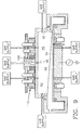
- FIG. 17A illustrates a variation of the embodiment of FIG. 5 in which the ceiling 52 and side wall 50 are separate semiconductor (e.g., silicon) pieces insulated from one another having separately controlled RF bias power levels applied to them from respective RF sources 210, 212 to enhance control over the center etch rate and selectivity relative to the edge.
- the ceiling 52 and side wall 50 are separate semiconductor (e.g., silicon) pieces insulated from one another having separately controlled RF bias power levels applied to them from respective RF sources 210, 212 to enhance control over the center etch rate and selectivity relative to the edge.
- the ceiling 52 may be a semiconductor (e.g., silicon) material doped so that it will act as an electrode capacitively coupling the RF bias power applied to it into the chamber 40 and simultaneously as a window through which RF power applied to the solenoid 42 may be inductively coupled into the chamber 40.
- a window-electrode is that an RF potential may be established directly over the wafer 56 (e.g., for controlling ion energy) while at the same time inductively coupling RF power directly over the wafer 56.
- This latter feature in combination with the separately controlled inner and outer solenoids 42, 90 and center and peripheral gas feeds 64a, 64b-d greatly enhances the ability to adjust various plasma process parameters such as ion density, ion energy, etch rate and etch selectivity at the workpiece center relative to the workpiece edge to achieve an optimum uniformity.
- the respective gas flow rates through individual gas feeds are individually and separately controlled to achieve such optimum uniformity of plasma process parameters.
- FIG. 17A illustrates how the lamp heaters 72 may be replaced by electric heating elements 72'.
- the disposable silicon member is an annular ring 62 surrounding the pedestal 54.
- FIG. 17B illustrates another variation in which the ceiling 52 itself may be divided into an inner disk 52a and an outer annulus 52b electrically insulated from one another and separately biased by independent RF power sources 214, 216 which may be separate outputs of a single differentially controlled RF power source.
- a user-accessible central controller 300 shown in FIGS. 17A and 17B such as a programmable electronic controller including, for example, a conventional microprocessor and memory, is connected to simultaneously control gas flow rates through the central gas feed 64a and the peripheral gas feeds 64b-d, RF plasma source power levels applied to the inner and outer antennas 42, 90 and RF bias power levels applied to the ceiling 52 and side wall 50 respectively (in FIG. 17A) and the RF bias power levels applied to the inner and outer ceiling portions 52a, 52b (in FIG. 17B), temperature of the ceiling 52 and the temperature of the silicon ring 62.
- a programmable electronic controller including, for example, a conventional microprocessor and memory
- a ceiling temperature controller 218 governs the power applied by a power source 220 to the heaters 72' by comparing the temperature measured by the ceiling temperature sensor 76 with a desired temperature known to the controller 300.
- a ring temperature controller 222 controls the power applied by a heater power source 224 to the heater lamps 77 facing the silicon ring 62 by comparing the ring temperature measured by the ring sensor 79 with a desired ring temperature stored known to the controller 222.
- the master controller 300 governs the desired temperatures of the temperature controllers 218 and 222, the RF power levels of the solenoid power sources 68, 96, the RF power levels of the bias power sources 210, 212 (FIG. 17A) or 214, 216 (FIG.
- the wafer bias level applied by the RF power source 70 and the gas flow rates supplied by the various gas supplies (or separate valves) to the gas inlets 64a-d is the RF potential difference between the wafer pedestal 54 and the ceiling 52.
- the pedestal RF power source 70 or the ceiling RF power source 210 may be simply a short to RF ground.
- the user can easily optimize apportionment of RF source power, RF bias power and gas flow rate between the workpiece center and periphery to achieve the greatest center-to-edge process uniformity across the surface of the workpiece (e.g., uniform radial distribution of etch rate and etch selectivity).
- the user can operate the reactor in a predominantly inductively coupled mode or in a predominantly capacitively coupled mode.
- the high thermal conductivity spacer 75, the ceiling 52 and the side wall 50 are integrally formed together from a single piece of crystalline silicon.
- RF sources depicted herein may derive their outputs from separate RF generators or from a common RF generator with different outputs at different RF power levels, frequencies and phases synthesized with variable power dividers, frequency multipliers and/or phase delays, as may be appropriate.
- process gas supplies may be derived from a common process gas supply which is divided among the plural separately controlled gas inlets 64.
Landscapes
- Chemical & Material Sciences (AREA)
- Engineering & Computer Science (AREA)
- Physics & Mathematics (AREA)
- Analytical Chemistry (AREA)
- Plasma & Fusion (AREA)
- General Chemical & Material Sciences (AREA)
- Chemical Kinetics & Catalysis (AREA)
- Oil, Petroleum & Natural Gas (AREA)
- Power Engineering (AREA)
- Manufacturing & Machinery (AREA)
- Computer Hardware Design (AREA)
- Microelectronics & Electronic Packaging (AREA)
- General Physics & Mathematics (AREA)
- Condensed Matter Physics & Semiconductors (AREA)
- Metallurgy (AREA)
- Materials Engineering (AREA)
- Mechanical Engineering (AREA)
- Inorganic Chemistry (AREA)
- Organic Chemistry (AREA)
- Health & Medical Sciences (AREA)
- Epidemiology (AREA)
- Public Health (AREA)
- Plasma Technology (AREA)
- Drying Of Semiconductors (AREA)
- ing And Chemical Polishing (AREA)
Applications Claiming Priority (2)
| Application Number | Priority Date | Filing Date | Title |
|---|---|---|---|
| US08/648,254 US6165311A (en) | 1991-06-27 | 1996-05-13 | Inductively coupled RF plasma reactor having an overhead solenoidal antenna |
| US648254 | 1996-05-13 |
Publications (1)
| Publication Number | Publication Date |
|---|---|
| EP0807953A1 true EP0807953A1 (en) | 1997-11-19 |
Family
ID=24600054
Family Applications (1)
| Application Number | Title | Priority Date | Filing Date |
|---|---|---|---|
| EP97303244A Withdrawn EP0807953A1 (en) | 1996-05-13 | 1997-05-13 | Inductively coupled RF plasma reactor having an overhead solenoidal antenna |
Country Status (5)
| Country | Link |
|---|---|
| US (4) | US6165311A (enExample) |
| EP (1) | EP0807953A1 (enExample) |
| JP (1) | JP4236294B2 (enExample) |
| KR (1) | KR970077318A (enExample) |
| TW (1) | TW329018B (enExample) |
Cited By (7)
| Publication number | Priority date | Publication date | Assignee | Title |
|---|---|---|---|---|
| EP0892422A3 (en) * | 1997-07-15 | 1999-04-14 | Applied Materials, Inc. | Improvements in or relating to plasma reactors |
| WO1999014784A3 (en) * | 1997-09-16 | 1999-06-03 | Lam Res Corp | Vacuum plasma processor having coil with added conducting segments to its peripheral part |
| WO2002080219A1 (en) * | 2001-03-30 | 2002-10-10 | Lam Research Corporation | Stacked rf excitation coil for inductive plasma processor |
| US6610212B2 (en) | 1998-04-24 | 2003-08-26 | Micron Technology, Inc. | Method of forming high aspect ratio apertures |
| US8444926B2 (en) | 2007-01-30 | 2013-05-21 | Applied Materials, Inc. | Processing chamber with heated chamber liner |
| EP2422359A4 (en) * | 2009-04-20 | 2013-07-03 | Applied Materials Inc | REINFORCED ABSORPTION OF RESTFLUORRADIKALEN WITH THE HELP OF A SILICONE COATING ON PROCESS CHAMBER WALLS |
| CN111638569A (zh) * | 2020-07-17 | 2020-09-08 | 中国人民解放军空军工程大学 | 一种射频感性耦合等离子体叠加相位梯度超表面吸波结构 |
Families Citing this family (135)
| Publication number | Priority date | Publication date | Assignee | Title |
|---|---|---|---|---|
| US6165311A (en) * | 1991-06-27 | 2000-12-26 | Applied Materials, Inc. | Inductively coupled RF plasma reactor having an overhead solenoidal antenna |
| US6063233A (en) | 1991-06-27 | 2000-05-16 | Applied Materials, Inc. | Thermal control apparatus for inductively coupled RF plasma reactor having an overhead solenoidal antenna |
| TW279240B (en) | 1995-08-30 | 1996-06-21 | Applied Materials Inc | Parallel-plate icp source/rf bias electrode head |
| US6231776B1 (en) | 1995-12-04 | 2001-05-15 | Daniel L. Flamm | Multi-temperature processing |
| US6534922B2 (en) * | 1996-09-27 | 2003-03-18 | Surface Technology Systems, Plc | Plasma processing apparatus |
| JP3567736B2 (ja) * | 1998-05-25 | 2004-09-22 | 株式会社日立製作所 | プラズマ処理装置 |
| JP4014300B2 (ja) * | 1998-06-19 | 2007-11-28 | 東京エレクトロン株式会社 | プラズマ処理装置 |
| EP1125314A1 (en) | 1998-07-10 | 2001-08-22 | Applied Materials, Inc. | Improved endpoint detection for substrate fabrication processes |
| JP2000315598A (ja) * | 1999-03-03 | 2000-11-14 | Anelva Corp | プラズマ処理装置 |
| JP3959200B2 (ja) * | 1999-03-19 | 2007-08-15 | 株式会社東芝 | 半導体装置の製造装置 |
| KR100338057B1 (ko) * | 1999-08-26 | 2002-05-24 | 황 철 주 | 유도 결합형 플라즈마 발생용 안테나 장치 |
| US6320320B1 (en) * | 1999-11-15 | 2001-11-20 | Lam Research Corporation | Method and apparatus for producing uniform process rates |
| KR20010047103A (ko) * | 1999-11-17 | 2001-06-15 | 윤종용 | 웨이퍼 식각장치 |
| KR100581998B1 (ko) * | 1999-11-17 | 2006-05-23 | 삼성전자주식회사 | 웨이퍼 식각장치 |
| JP3645768B2 (ja) * | 1999-12-07 | 2005-05-11 | シャープ株式会社 | プラズマプロセス装置 |
| US6598559B1 (en) | 2000-03-24 | 2003-07-29 | Applied Materials, Inc. | Temperature controlled chamber |
| US7096819B2 (en) * | 2001-03-30 | 2006-08-29 | Lam Research Corporation | Inductive plasma processor having coil with plural windings and method of controlling plasma density |
| US6554954B2 (en) | 2001-04-03 | 2003-04-29 | Applied Materials Inc. | Conductive collar surrounding semiconductor workpiece in plasma chamber |
| US6676760B2 (en) * | 2001-08-16 | 2004-01-13 | Appiled Materials, Inc. | Process chamber having multiple gas distributors and method |
| WO2003030239A1 (en) * | 2001-09-28 | 2003-04-10 | Sumitomo Precision Products Co., Ltd. | Silicon substrate etching method and etching apparatus |
| US7084832B2 (en) * | 2001-10-09 | 2006-08-01 | Plasma Control Systems, Llc | Plasma production device and method and RF driver circuit with adjustable duty cycle |
| US7132996B2 (en) * | 2001-10-09 | 2006-11-07 | Plasma Control Systems Llc | Plasma production device and method and RF driver circuit |
| US7100532B2 (en) * | 2001-10-09 | 2006-09-05 | Plasma Control Systems, Llc | Plasma production device and method and RF driver circuit with adjustable duty cycle |
| US6597117B2 (en) * | 2001-11-30 | 2003-07-22 | Samsung Austin Semiconductor, L.P. | Plasma coil |
| US20030141178A1 (en) * | 2002-01-30 | 2003-07-31 | Applied Materials, Inc. | Energizing gas for substrate processing with shockwaves |
| TWI241868B (en) * | 2002-02-06 | 2005-10-11 | Matsushita Electric Industrial Co Ltd | Plasma processing method and apparatus |
| US6737358B2 (en) * | 2002-02-13 | 2004-05-18 | Intel Corporation | Plasma etching uniformity control |
| JP3820188B2 (ja) * | 2002-06-19 | 2006-09-13 | 三菱重工業株式会社 | プラズマ処理装置及びプラズマ処理方法 |
| JP2004047696A (ja) * | 2002-07-11 | 2004-02-12 | Matsushita Electric Ind Co Ltd | プラズマドーピング方法及び装置、整合回路 |
| US20040018741A1 (en) * | 2002-07-26 | 2004-01-29 | Applied Materials, Inc. | Method For Enhancing Critical Dimension Uniformity After Etch |
| US20040025791A1 (en) * | 2002-08-09 | 2004-02-12 | Applied Materials, Inc. | Etch chamber with dual frequency biasing sources and a single frequency plasma generating source |
| US6837937B2 (en) * | 2002-08-27 | 2005-01-04 | Hitachi High-Technologies Corporation | Plasma processing apparatus |
| KR100457844B1 (ko) * | 2002-08-27 | 2004-11-18 | 삼성전자주식회사 | 반도체 장치의 식각 방법 |
| JP4753276B2 (ja) * | 2002-11-26 | 2011-08-24 | 東京エレクトロン株式会社 | プラズマ処理方法及びプラズマ処理装置 |
| US6872909B2 (en) * | 2003-04-16 | 2005-03-29 | Applied Science And Technology, Inc. | Toroidal low-field reactive gas and plasma source having a dielectric vacuum vessel |
| US6905624B2 (en) * | 2003-07-07 | 2005-06-14 | Applied Materials, Inc. | Interferometric endpoint detection in a substrate etching process |
| US20050178336A1 (en) * | 2003-07-15 | 2005-08-18 | Heng Liu | Chemical vapor deposition reactor having multiple inlets |
| US20050011459A1 (en) * | 2003-07-15 | 2005-01-20 | Heng Liu | Chemical vapor deposition reactor |
| US20050106873A1 (en) * | 2003-08-15 | 2005-05-19 | Hoffman Daniel J. | Plasma chamber having multiple RF source frequencies |
| KR101038204B1 (ko) * | 2004-02-25 | 2011-05-31 | 주성엔지니어링(주) | 플라즈마 발생용 안테나 |
| US20050227382A1 (en) * | 2004-04-02 | 2005-10-13 | Hui Angela T | In-situ surface treatment for memory cell formation |
| JP4550507B2 (ja) * | 2004-07-26 | 2010-09-22 | 株式会社日立ハイテクノロジーズ | プラズマ処理装置 |
| US7886688B2 (en) * | 2004-09-29 | 2011-02-15 | Sekisui Chemical Co., Ltd. | Plasma processing apparatus |
| US8328942B2 (en) * | 2004-12-17 | 2012-12-11 | Lam Research Corporation | Wafer heating and temperature control by backside fluid injection |
| JP2006216903A (ja) * | 2005-02-07 | 2006-08-17 | Hitachi High-Technologies Corp | プラズマ処理装置 |
| JP2006237479A (ja) * | 2005-02-28 | 2006-09-07 | Mitsubishi Heavy Ind Ltd | プラズマ処理装置 |
| US7674393B2 (en) | 2005-03-25 | 2010-03-09 | Tokyo Electron Limited | Etching method and apparatus |
| US7651587B2 (en) * | 2005-08-11 | 2010-01-26 | Applied Materials, Inc. | Two-piece dome with separate RF coils for inductively coupled plasma reactors |
| US7695633B2 (en) * | 2005-10-18 | 2010-04-13 | Applied Materials, Inc. | Independent control of ion density, ion energy distribution and ion dissociation in a plasma reactor |
| US8911590B2 (en) * | 2006-02-27 | 2014-12-16 | Lam Research Corporation | Integrated capacitive and inductive power sources for a plasma etching chamber |
| JP4782585B2 (ja) * | 2006-02-28 | 2011-09-28 | 株式会社日立ハイテクノロジーズ | プラズマエッチング装置及び方法 |
| US8187415B2 (en) * | 2006-04-21 | 2012-05-29 | Applied Materials, Inc. | Plasma etch reactor with distribution of etch gases across a wafer surface and a polymer oxidizing gas in an independently fed center gas zone |
| US20070249173A1 (en) * | 2006-04-21 | 2007-10-25 | Applied Materials, Inc. | Plasma etch process using etch uniformity control by using compositionally independent gas feed |
| US20070245961A1 (en) * | 2006-04-24 | 2007-10-25 | Applied Materials, Inc. | Dual plasma source process using a variable frequency capacitively coupled source for controlling plasma ion dissociation |
| US7645357B2 (en) * | 2006-04-24 | 2010-01-12 | Applied Materials, Inc. | Plasma reactor apparatus with a VHF capacitively coupled plasma source of variable frequency |
| US20070246163A1 (en) * | 2006-04-24 | 2007-10-25 | Applied Materials, Inc. | Plasma reactor apparatus with independent capacitive and inductive plasma sources |
| US20070246162A1 (en) * | 2006-04-24 | 2007-10-25 | Applied Materials, Inc. | Plasma reactor apparatus with an inductive plasma source and a VHF capacitively coupled plasma source with variable frequency |
| US20070246443A1 (en) * | 2006-04-24 | 2007-10-25 | Applied Materials, Inc. | Process using combined capacitively and inductively coupled plasma process for controlling plasma ion dissociation |
| US20070245960A1 (en) * | 2006-04-24 | 2007-10-25 | Applied Materials, Inc. | Process using combined capacitively and inductively coupled plasma sources for controlling plasma ion density |
| US20070245958A1 (en) * | 2006-04-24 | 2007-10-25 | Applied Materials, Inc. | Dual plasma source process using a variable frequency capacitively coupled source for controlling ion radial distribution |
| US7727413B2 (en) * | 2006-04-24 | 2010-06-01 | Applied Materials, Inc. | Dual plasma source process using a variable frequency capacitively coupled source to control plasma ion density |
| US20070246161A1 (en) * | 2006-04-24 | 2007-10-25 | Applied Materials, Inc. | Plasma reactor apparatus with a toroidal plasma source and a VHF capacitively coupled plasma source with variable frequency |
| US7780864B2 (en) * | 2006-04-24 | 2010-08-24 | Applied Materials, Inc. | Process using combined capacitively and inductively coupled plasma sources for controlling plasma ion radial distribution |
| US7264688B1 (en) | 2006-04-24 | 2007-09-04 | Applied Materials, Inc. | Plasma reactor apparatus with independent capacitive and toroidal plasma sources |
| US20070254483A1 (en) * | 2006-04-28 | 2007-11-01 | Applied Materials, Inc. | Plasma etch process using polymerizing etch gases and an inert diluent gas in independent gas injection zones to improve etch profile or etch rate uniformity |
| US7540971B2 (en) * | 2006-04-28 | 2009-06-02 | Applied Materials, Inc. | Plasma etch process using polymerizing etch gases across a wafer surface and additional polymer managing or controlling gases in independently fed gas zones with time and spatial modulation of gas content |
| US7541292B2 (en) * | 2006-04-28 | 2009-06-02 | Applied Materials, Inc. | Plasma etch process with separately fed carbon-lean and carbon-rich polymerizing etch gases in independent inner and outer gas injection zones |
| US7431859B2 (en) * | 2006-04-28 | 2008-10-07 | Applied Materials, Inc. | Plasma etch process using polymerizing etch gases with different etch and polymer-deposition rates in different radial gas injection zones with time modulation |
| CN101136279B (zh) * | 2006-08-28 | 2010-05-12 | 北京北方微电子基地设备工艺研究中心有限责任公司 | 电感耦合线圈及电感耦合等离子体装置 |
| US7845310B2 (en) * | 2006-12-06 | 2010-12-07 | Axcelis Technologies, Inc. | Wide area radio frequency plasma apparatus for processing multiple substrates |
| US8956500B2 (en) * | 2007-04-24 | 2015-02-17 | Applied Materials, Inc. | Methods to eliminate “M-shape” etch rate profile in inductively coupled plasma reactor |
| US20090096349A1 (en) * | 2007-04-26 | 2009-04-16 | Moshtagh Vahid S | Cross flow cvd reactor |
| US8216419B2 (en) * | 2008-03-28 | 2012-07-10 | Bridgelux, Inc. | Drilled CVD shower head |
| US20090004873A1 (en) * | 2007-06-26 | 2009-01-01 | Intevac, Inc. | Hybrid etch chamber with decoupled plasma controls |
| US7879250B2 (en) * | 2007-09-05 | 2011-02-01 | Applied Materials, Inc. | Method of processing a workpiece in a plasma reactor with independent wafer edge process gas injection |
| US7832354B2 (en) * | 2007-09-05 | 2010-11-16 | Applied Materials, Inc. | Cathode liner with wafer edge gas injection in a plasma reactor chamber |
| JP5347294B2 (ja) * | 2007-09-12 | 2013-11-20 | 東京エレクトロン株式会社 | 成膜装置、成膜方法及び記憶媒体 |
| US8668775B2 (en) * | 2007-10-31 | 2014-03-11 | Toshiba Techno Center Inc. | Machine CVD shower head |
| KR100881954B1 (ko) * | 2007-11-09 | 2009-02-06 | 한국전자통신연구원 | 반응성 스퍼터링 증착 장치 |
| US8062472B2 (en) * | 2007-12-19 | 2011-11-22 | Applied Materials, Inc. | Method of correcting baseline skew by a novel motorized source coil assembly |
| US8137463B2 (en) * | 2007-12-19 | 2012-03-20 | Applied Materials, Inc. | Dual zone gas injection nozzle |
| US8999106B2 (en) * | 2007-12-19 | 2015-04-07 | Applied Materials, Inc. | Apparatus and method for controlling edge performance in an inductively coupled plasma chamber |
| US20090162570A1 (en) * | 2007-12-19 | 2009-06-25 | Applied Materials, Inc. | Apparatus and method for processing a substrate using inductively coupled plasma technology |
| US8066895B2 (en) * | 2008-02-28 | 2011-11-29 | Applied Materials, Inc. | Method to control uniformity using tri-zone showerhead |
| US20090220865A1 (en) * | 2008-02-29 | 2009-09-03 | Applied Materials, Inc. | Method and apparatus for source field shaping in a plasma etch reactor |
| US8849585B2 (en) * | 2008-06-26 | 2014-09-30 | Lam Research Corporation | Methods for automatically characterizing a plasma |
| US8164349B2 (en) | 2008-07-07 | 2012-04-24 | Lam Research Corporation | Capacitively-coupled electrostatic (CCE) probe arrangement for detecting strike step in a plasma processing chamber and methods thereof |
| WO2010005932A2 (en) * | 2008-07-07 | 2010-01-14 | Lam Research Corporation | Plasma-facing probe arrangement including vacuum gap for use in a plasma processing chamber |
| CN102084471B (zh) | 2008-07-07 | 2012-11-28 | 朗姆研究公司 | 用于检测等离子体处理室中的等离子体不稳定的无源电容耦合静电(cce)探针装置 |
| TWI458850B (zh) * | 2008-07-07 | 2014-11-01 | Lam Res Corp | 用來鑑定電漿處理腔室中之薄膜之特性的射頻偏壓電容耦合靜電探針裝置 |
| WO2010005929A2 (en) | 2008-07-07 | 2010-01-14 | Lam Research Corporation | Passive capacitively-coupled electrostatic (cce) probe arrangement for detecting in-situ arcing events in a plasma processing chamber |
| WO2010005931A2 (en) * | 2008-07-07 | 2010-01-14 | Lam Research Corporation | Capacitively-coupled electrostatic (cce) probe arrangement for detecting dechucking in a plasma processing chamber and methods thereof |
| US8540844B2 (en) * | 2008-12-19 | 2013-09-24 | Lam Research Corporation | Plasma confinement structures in plasma processing systems |
| US8627783B2 (en) * | 2008-12-19 | 2014-01-14 | Lam Research Corporation | Combined wafer area pressure control and plasma confinement assembly |
| US20100297347A1 (en) * | 2009-04-24 | 2010-11-25 | Applied Materials, Inc. | Substrate support having side gas outlets and methods |
| US20110120375A1 (en) * | 2009-11-23 | 2011-05-26 | Jusung Engineering Co., Ltd. | Apparatus for processing substrate |
| US8591755B2 (en) * | 2010-09-15 | 2013-11-26 | Lam Research Corporation | Methods for controlling plasma constituent flux and deposition during semiconductor fabrication and apparatus for implementing the same |
| US9653264B2 (en) * | 2010-12-17 | 2017-05-16 | Mattson Technology, Inc. | Inductively coupled plasma source for plasma processing |
| US20120152900A1 (en) * | 2010-12-20 | 2012-06-21 | Applied Materials, Inc. | Methods and apparatus for gas delivery into plasma processing chambers |
| US8808561B2 (en) * | 2011-11-15 | 2014-08-19 | Lam Research Coporation | Inert-dominant pulsing in plasma processing systems |
| JP5929429B2 (ja) * | 2012-03-30 | 2016-06-08 | 東京エレクトロン株式会社 | 成膜装置 |
| JP6011417B2 (ja) * | 2012-06-15 | 2016-10-19 | 東京エレクトロン株式会社 | 成膜装置、基板処理装置及び成膜方法 |
| KR102104018B1 (ko) * | 2013-03-12 | 2020-04-23 | 어플라이드 머티어리얼스, 인코포레이티드 | 방위각 및 방사상 분배 제어되는 다중-구역 가스 주입 조립체 |
| JP6362670B2 (ja) * | 2013-03-15 | 2018-07-25 | アプライド マテリアルズ インコーポレイテッドApplied Materials,Incorporated | ポリマーを管理することによるエッチングシステムの生産性の向上 |
| US9275869B2 (en) | 2013-08-02 | 2016-03-01 | Lam Research Corporation | Fast-gas switching for etching |
| JP6169701B2 (ja) | 2013-08-09 | 2017-07-26 | 東京エレクトロン株式会社 | プラズマ処理装置及びプラズマ処理方法 |
| US20150162169A1 (en) * | 2013-12-05 | 2015-06-11 | Taiwan Semiconductor Manufacturing Co., Ltd. | Etching apparatus and method |
| CN104743496B (zh) * | 2013-12-29 | 2017-03-22 | 北京北方微电子基地设备工艺研究中心有限责任公司 | 深硅刻蚀方法和用于深硅刻蚀的设备 |
| US10249511B2 (en) | 2014-06-27 | 2019-04-02 | Lam Research Corporation | Ceramic showerhead including central gas injector for tunable convective-diffusive gas flow in semiconductor substrate processing apparatus |
| WO2016040547A1 (en) | 2014-09-11 | 2016-03-17 | Massachusetts Institute Of Technology | Processing system for small substrates |
| US10658222B2 (en) | 2015-01-16 | 2020-05-19 | Lam Research Corporation | Moveable edge coupling ring for edge process control during semiconductor wafer processing |
| CN113382551B (zh) * | 2015-05-06 | 2025-01-10 | 哈钦森技术股份有限公司 | 用于硬盘驱动器的挠曲部的等离子体处理 |
| CN104918401A (zh) * | 2015-05-26 | 2015-09-16 | 山东专利工程总公司 | 一种感应耦合型等离子体处理装置 |
| US10957561B2 (en) | 2015-07-30 | 2021-03-23 | Lam Research Corporation | Gas delivery system |
| US10825659B2 (en) | 2016-01-07 | 2020-11-03 | Lam Research Corporation | Substrate processing chamber including multiple gas injection points and dual injector |
| US10651015B2 (en) | 2016-02-12 | 2020-05-12 | Lam Research Corporation | Variable depth edge ring for etch uniformity control |
| US10699878B2 (en) * | 2016-02-12 | 2020-06-30 | Lam Research Corporation | Chamber member of a plasma source and pedestal with radially outward positioned lift pins for translation of a substrate c-ring |
| US10410832B2 (en) | 2016-08-19 | 2019-09-10 | Lam Research Corporation | Control of on-wafer CD uniformity with movable edge ring and gas injection adjustment |
| US10504720B2 (en) | 2016-11-29 | 2019-12-10 | Taiwan Semiconductor Manufacturing Company, Ltd. | Etching using chamber with top plate formed of non-oxygen containing material |
| US11424104B2 (en) | 2017-04-24 | 2022-08-23 | Applied Materials, Inc. | Plasma reactor with electrode filaments extending from ceiling |
| US10510515B2 (en) | 2017-06-22 | 2019-12-17 | Applied Materials, Inc. | Processing tool with electrically switched electrode assembly |
| US11355321B2 (en) | 2017-06-22 | 2022-06-07 | Applied Materials, Inc. | Plasma reactor with electrode assembly for moving substrate |
| US11114284B2 (en) * | 2017-06-22 | 2021-09-07 | Applied Materials, Inc. | Plasma reactor with electrode array in ceiling |
| CN118380375A (zh) | 2017-11-21 | 2024-07-23 | 朗姆研究公司 | 底部边缘环和中部边缘环 |
| WO2019124119A1 (ja) * | 2017-12-21 | 2019-06-27 | 東京エレクトロン株式会社 | 基板支持部材、基板処理装置及び基板搬送装置 |
| US11153960B1 (en) * | 2018-06-08 | 2021-10-19 | Innoveering, LLC | Plasma-based electro-optical sensing and methods |
| US11114306B2 (en) * | 2018-09-17 | 2021-09-07 | Applied Materials, Inc. | Methods for depositing dielectric material |
| KR102041518B1 (ko) * | 2019-07-18 | 2019-11-06 | 에이피티씨 주식회사 | 분리형 플라즈마 소스 코일 및 이의 제어 방법 |
| JP7466686B2 (ja) | 2020-03-23 | 2024-04-12 | ラム リサーチ コーポレーション | 基板処理システムにおける中間リング腐食補償 |
| US12033835B2 (en) * | 2020-06-10 | 2024-07-09 | Applied Materials, Inc. | Modular microwave source with multiple metal housings |
| CN112011774B (zh) * | 2020-08-25 | 2022-09-16 | 北京北方华创微电子装备有限公司 | 半导体设备及其半导体腔室以及半导体冷却方法 |
| KR102787323B1 (ko) | 2020-09-24 | 2025-03-27 | 삼성전자주식회사 | 플라즈마 처리 장치 및 플라즈마 처리 방법 |
| JP2024535295A (ja) * | 2021-09-20 | 2024-09-30 | ラム リサーチ コーポレーション | Icp源におけるrf電力の増加を軽減するための筐体 |
| KR102696031B1 (ko) * | 2022-04-26 | 2024-08-16 | 주식회사 테스 | 램프유닛 및 하이브리드 챔버 |
| US12074390B2 (en) | 2022-11-11 | 2024-08-27 | Tokyo Electron Limited | Parallel resonance antenna for radial plasma control |
Citations (9)
| Publication number | Priority date | Publication date | Assignee | Title |
|---|---|---|---|---|
| EP0403418A2 (en) * | 1989-06-13 | 1990-12-19 | PLASMA & MATERIALS TECHNOLOGIES, INC. | High density plasma deposition and etching apparatus |
| EP0413282A2 (en) * | 1989-08-14 | 1991-02-20 | Lam Research Corporation | Method and apparatus for producing magnetically-coupled planar plasma |
| US5277751A (en) * | 1992-06-18 | 1994-01-11 | Ogle John S | Method and apparatus for producing low pressure planar plasma using a coil with its axis parallel to the surface of a coupling window |
| JPH06196446A (ja) * | 1992-12-24 | 1994-07-15 | Nec Corp | 高周波磁場励起処理装置 |
| JPH07288196A (ja) * | 1994-02-22 | 1995-10-31 | Tokyo Electron Ltd | プラズマ発生装置 |
| EP0680072A2 (en) * | 1994-04-28 | 1995-11-02 | Applied Materials, Inc. | A method of operating a high density plasma CVD reactor with combined inductive and capacitive coupling |
| JPH0817799A (ja) * | 1994-06-28 | 1996-01-19 | Plasma Syst:Kk | プラズマ処理装置 |
| EP0727807A1 (en) * | 1995-02-15 | 1996-08-21 | Applied Materials, Inc. | Plasma reactor |
| EP0742577A2 (en) * | 1995-05-08 | 1996-11-13 | Applied Materials, Inc. | Inductively and multi-capacitively coupled plasma reactor |
Family Cites Families (133)
| Publication number | Priority date | Publication date | Assignee | Title |
|---|---|---|---|---|
| GB231197A (en) | 1924-03-24 | 1925-08-06 | Peter August Nordling | Improvement in hooks and the like |
| DE2518853C3 (de) * | 1975-04-28 | 1979-03-22 | Siemens Ag, 1000 Berlin Und 8000 Muenchen | Vorrichtung zum Abscheiden von elementarem Silicium aus einem Reaktionsgas |
| GB1550853A (en) * | 1975-10-06 | 1979-08-22 | Hitachi Ltd | Apparatus and process for plasma treatment |
| US4233109A (en) | 1976-01-16 | 1980-11-11 | Zaidan Hojin Handotai Kenkyu Shinkokai | Dry etching method |
| JPS559464A (en) | 1978-07-07 | 1980-01-23 | Toshiba Corp | Production method of bipolar integrated circuit containing i2 l |
| JPS55154582A (en) * | 1979-05-21 | 1980-12-02 | Chiyou Lsi Gijutsu Kenkyu Kumiai | Gas plasma etching method |
| US4261762A (en) * | 1979-09-14 | 1981-04-14 | Eaton Corporation | Method for conducting heat to or from an article being treated under vacuum |
| JPS6056431B2 (ja) * | 1980-10-09 | 1985-12-10 | 三菱電機株式会社 | プラズマエツチング装置 |
| JPS57155732A (en) * | 1981-03-20 | 1982-09-25 | Sharp Corp | Dry etching |
| US4368092A (en) | 1981-04-02 | 1983-01-11 | The Perkin-Elmer Corporation | Apparatus for the etching for semiconductor devices |
| US4350578A (en) * | 1981-05-11 | 1982-09-21 | International Business Machines Corporation | Cathode for etching |
| US4427516A (en) * | 1981-08-24 | 1984-01-24 | Bell Telephone Laboratories, Incorporated | Apparatus and method for plasma-assisted etching of wafers |
| EP0082015A1 (en) * | 1981-12-16 | 1983-06-22 | Konica Corporation | Method of forming an image with a photographic cuprous halide material |
| US4512391A (en) * | 1982-01-29 | 1985-04-23 | Varian Associates, Inc. | Apparatus for thermal treatment of semiconductor wafers by gas conduction incorporating peripheral gas inlet |
| US4457359A (en) * | 1982-05-25 | 1984-07-03 | Varian Associates, Inc. | Apparatus for gas-assisted, solid-to-solid thermal transfer with a semiconductor wafer |
| JPS6060060A (ja) * | 1983-09-12 | 1985-04-06 | 株式会社日立製作所 | 鉄道車両の扉開閉装置 |
| US4579080A (en) | 1983-12-09 | 1986-04-01 | Applied Materials, Inc. | Induction heated reactor system for chemical vapor deposition |
| JPS6191377A (ja) * | 1984-10-12 | 1986-05-09 | Anelva Corp | 表面処理装置 |
| US4735902A (en) | 1984-10-23 | 1988-04-05 | Matti Siren | Stabilized composition containing inositoltriphosphate |
| JPH07118474B2 (ja) * | 1984-12-17 | 1995-12-18 | ソニー株式会社 | エツチングガス及びこれを用いたエツチング方法 |
| JPS61147531A (ja) * | 1984-12-21 | 1986-07-05 | Toshiba Corp | 反応性イオンエツチング方法 |
| US4572759A (en) | 1984-12-26 | 1986-02-25 | Benzing Technology, Inc. | Troide plasma reactor with magnetic enhancement |
| US4870245A (en) * | 1985-04-01 | 1989-09-26 | Motorola, Inc. | Plasma enhanced thermal treatment apparatus |
| US4810935A (en) * | 1985-05-03 | 1989-03-07 | The Australian National University | Method and apparatus for producing large volume magnetoplasmas |
| JPS627268A (ja) | 1985-07-03 | 1987-01-14 | Nec Corp | フアクシミリ装置 |
| JPS6212129A (ja) * | 1985-07-10 | 1987-01-21 | Hitachi Ltd | プラズマ処理装置 |
| US4711698A (en) * | 1985-07-15 | 1987-12-08 | Texas Instruments Incorporated | Silicon oxide thin film etching process |
| US4807016A (en) * | 1985-07-15 | 1989-02-21 | Texas Instruments Incorporated | Dry etch of phosphosilicate glass with selectivity to undoped oxide |
| JPH0680650B2 (ja) | 1986-04-23 | 1994-10-12 | 株式会社日立マイコンシステム | 半導体集積回路装置の製造方法 |
| JPS62254428A (ja) * | 1986-04-28 | 1987-11-06 | Nippon Telegr & Teleph Corp <Ntt> | 反応性スパツタエツチング方法と反応性スパツタエツチング装置 |
| DE3717985A1 (de) | 1986-05-28 | 1987-12-03 | Minolta Camera Kk | Elektrochrome vorrichtung |
| JPS639120A (ja) * | 1986-06-30 | 1988-01-14 | Canon Inc | ドライエツチング用ウエハステ−ジ |
| US4755345A (en) * | 1986-08-01 | 1988-07-05 | The United States Of America As Represented By The United States Department Of Energy | Impedance matched, high-power, rf antenna for ion cyclotron resonance heating of a plasma |
| US4786352A (en) * | 1986-09-12 | 1988-11-22 | Benzing Technologies, Inc. | Apparatus for in-situ chamber cleaning |
| US4859908A (en) | 1986-09-24 | 1989-08-22 | Matsushita Electric Industrial Co., Ltd. | Plasma processing apparatus for large area ion irradiation |
| DE3632340C2 (de) | 1986-09-24 | 1998-01-15 | Leybold Ag | Induktiv angeregte Ionenquelle |
| KR900007687B1 (ko) | 1986-10-17 | 1990-10-18 | 가부시기가이샤 히다찌세이사꾸쇼 | 플라즈마처리방법 및 장치 |
| US4756810A (en) * | 1986-12-04 | 1988-07-12 | Machine Technology, Inc. | Deposition and planarizing methods and apparatus |
| GB8629634D0 (en) | 1986-12-11 | 1987-01-21 | Dobson C D | Reactive ion & sputter etching |
| US4842683A (en) * | 1986-12-19 | 1989-06-27 | Applied Materials, Inc. | Magnetic field-enhanced plasma etch reactor |
| US5000113A (en) * | 1986-12-19 | 1991-03-19 | Applied Materials, Inc. | Thermal CVD/PECVD reactor and use for thermal chemical vapor deposition of silicon dioxide and in-situ multi-step planarized process |
| JPS63155728A (ja) | 1986-12-19 | 1988-06-28 | Canon Inc | プラズマ処理装置 |
| US4793897A (en) * | 1987-03-20 | 1988-12-27 | Applied Materials, Inc. | Selective thin film etch process |
| US4786359A (en) * | 1987-06-24 | 1988-11-22 | Tegal Corporation | Xenon enhanced plasma etch |
| JPS6415928A (en) | 1987-07-10 | 1989-01-19 | Hitachi Ltd | Dry etching method |
| JPH0741153Y2 (ja) * | 1987-10-26 | 1995-09-20 | 東京応化工業株式会社 | 試料処理用電極 |
| DE58904540D1 (de) * | 1988-03-24 | 1993-07-08 | Siemens Ag | Verfahren und vorrichtung zum herstellen von aus amorphen silizium-germanium-legierungen bestehenden halbleiterschichten nach der glimmentladungstechnik, insbesondere fuer solarzellen. |
| JPH01296600A (ja) * | 1988-05-23 | 1989-11-29 | Nissin Electric Co Ltd | プラズマ発生源 |
| JPH02148235A (ja) | 1988-11-30 | 1990-06-07 | Toshiba Corp | データ退避方式 |
| US4918031A (en) * | 1988-12-28 | 1990-04-17 | American Telephone And Telegraph Company,At&T Bell Laboratories | Processes depending on plasma generation using a helical resonator |
| US5015330A (en) * | 1989-02-28 | 1991-05-14 | Kabushiki Kaisha Toshiba | Film forming method and film forming device |
| US5421891A (en) | 1989-06-13 | 1995-06-06 | Plasma & Materials Technologies, Inc. | High density plasma deposition and etching apparatus |
| US5122251A (en) | 1989-06-13 | 1992-06-16 | Plasma & Materials Technologies, Inc. | High density plasma deposition and etching apparatus |
| US5556501A (en) * | 1989-10-03 | 1996-09-17 | Applied Materials, Inc. | Silicon scavenger in an inductively coupled RF plasma reactor |
| US5032202A (en) | 1989-10-03 | 1991-07-16 | Martin Marietta Energy Systems, Inc. | Plasma generating apparatus for large area plasma processing |
| US5210466A (en) | 1989-10-03 | 1993-05-11 | Applied Materials, Inc. | VHF/UHF reactor system |
| US5142198A (en) * | 1989-12-21 | 1992-08-25 | Applied Science And Technology, Inc. | Microwave reactive gas discharge device |
| DE3942964A1 (de) | 1989-12-23 | 1991-06-27 | Leybold Ag | Einrichtung fuer die erzeugung eines plasmas |
| US5203956A (en) * | 1990-01-08 | 1993-04-20 | Lsi Logic Corporation | Method for performing in-situ etch of a CVD chamber |
| US5085727A (en) * | 1990-05-21 | 1992-02-04 | Applied Materials, Inc. | Plasma etch apparatus with conductive coating on inner metal surfaces of chamber to provide protection from chemical corrosion |
| US5707486A (en) | 1990-07-31 | 1998-01-13 | Applied Materials, Inc. | Plasma reactor using UHF/VHF and RF triode source, and process |
| US5258824A (en) * | 1990-08-09 | 1993-11-02 | Applied Materials, Inc. | In-situ measurement of a thin film deposited on a wafer |
| US5169487A (en) * | 1990-08-27 | 1992-12-08 | Micron Technology, Inc. | Anisotropic etch method |
| US5074456A (en) * | 1990-09-18 | 1991-12-24 | Lam Research Corporation | Composite electrode for plasma processes |
| US5356515A (en) | 1990-10-19 | 1994-10-18 | Tokyo Electron Limited | Dry etching method |
| EP0484908A3 (en) | 1990-11-08 | 1993-04-07 | Lonza A.G. | Microbiological process for the preparation of hydroxylated pyrazinederivatives |
| EP0489407A3 (en) | 1990-12-03 | 1992-07-22 | Applied Materials, Inc. | Plasma reactor using uhf/vhf resonant antenna source, and processes |
| EP0584252B1 (en) * | 1991-05-17 | 1998-03-04 | Lam Research Corporation | A PROCESS FOR DEPOSITING A SIOx FILM HAVING REDUCED INTRINSIC STRESS AND/OR REDUCED HYDROGEN CONTENT |
| US6063233A (en) | 1991-06-27 | 2000-05-16 | Applied Materials, Inc. | Thermal control apparatus for inductively coupled RF plasma reactor having an overhead solenoidal antenna |
| US5392018A (en) * | 1991-06-27 | 1995-02-21 | Applied Materials, Inc. | Electronically tuned matching networks using adjustable inductance elements and resonant tank circuits |
| US6036877A (en) | 1991-06-27 | 2000-03-14 | Applied Materials, Inc. | Plasma reactor with heated source of a polymer-hardening precursor material |
| US6095083A (en) * | 1991-06-27 | 2000-08-01 | Applied Materiels, Inc. | Vacuum processing chamber having multi-mode access |
| KR100255703B1 (ko) * | 1991-06-27 | 2000-05-01 | 조셉 제이. 스위니 | 전자기 rf연결부를 사용하는 플라즈마 처리기 및 방법 |
| US6074512A (en) | 1991-06-27 | 2000-06-13 | Applied Materials, Inc. | Inductively coupled RF plasma reactor having an overhead solenoidal antenna and modular confinement magnet liners |
| US5187454A (en) * | 1992-01-23 | 1993-02-16 | Applied Materials, Inc. | Electronically tuned matching network using predictor-corrector control system |
| US6090303A (en) * | 1991-06-27 | 2000-07-18 | Applied Materials, Inc. | Process for etching oxides in an electromagnetically coupled planar plasma apparatus |
| US6165311A (en) * | 1991-06-27 | 2000-12-26 | Applied Materials, Inc. | Inductively coupled RF plasma reactor having an overhead solenoidal antenna |
| US5477975A (en) * | 1993-10-15 | 1995-12-26 | Applied Materials Inc | Plasma etch apparatus with heated scavenging surfaces |
| US6024826A (en) | 1996-05-13 | 2000-02-15 | Applied Materials, Inc. | Plasma reactor with heated source of a polymer-hardening precursor material |
| US6077384A (en) * | 1994-08-11 | 2000-06-20 | Applied Materials, Inc. | Plasma reactor having an inductive antenna coupling power through a parallel plate electrode |
| US5164945A (en) * | 1991-07-01 | 1992-11-17 | Laser Centers Of America, Inc. | Laser device with intermediate refraction index layer for reduced fresnel losses |
| KR100297358B1 (ko) | 1991-07-23 | 2001-11-30 | 히가시 데쓰로 | 플라즈마에칭장치 |
| US5249251A (en) * | 1991-09-16 | 1993-09-28 | The United States Of America As Represented By The Administrator Of The National Aeronautics And Space Administration | Optical fiber sensor having an active core |
| US5275683A (en) | 1991-10-24 | 1994-01-04 | Tokyo Electron Limited | Mount for supporting substrates and plasma processing apparatus using the same |
| JP3221025B2 (ja) * | 1991-12-19 | 2001-10-22 | ソニー株式会社 | プラズマプロセス装置 |
| US5349313A (en) * | 1992-01-23 | 1994-09-20 | Applied Materials Inc. | Variable RF power splitter |
| US5423945A (en) * | 1992-09-08 | 1995-06-13 | Applied Materials, Inc. | Selectivity for etching an oxide over a nitride |
| DE69226253T2 (de) * | 1992-01-24 | 1998-12-17 | Applied Materials, Inc., Santa Clara, Calif. | Plasmaätzverfahren und Reaktor zur Plasmabearbeitung |
| EP0552490A1 (en) * | 1992-01-24 | 1993-07-28 | Applied Materials, Inc. | Process for etching an oxide layer over a nitride |
| US5241245A (en) * | 1992-05-06 | 1993-08-31 | International Business Machines Corporation | Optimized helical resonator for plasma processing |
| US5286344A (en) | 1992-06-15 | 1994-02-15 | Micron Technology, Inc. | Process for selectively etching a layer of silicon dioxide on an underlying stop layer of silicon nitride |
| JP2625072B2 (ja) * | 1992-09-08 | 1997-06-25 | アプライド マテリアルズ インコーポレイテッド | 電磁rf結合を用いたプラズマ反応装置及びその方法 |
| US5346578A (en) | 1992-11-04 | 1994-09-13 | Novellus Systems, Inc. | Induction plasma source |
| KR100281345B1 (ko) * | 1992-12-01 | 2001-03-02 | 조셉 제이. 스위니 | 전자기 결합성 플래너 플라즈마 장치에서의 산화물 에칭 공정 |
| KR100238627B1 (ko) * | 1993-01-12 | 2000-01-15 | 히가시 데쓰로 | 플라즈마 처리장치 |
| US5401350A (en) * | 1993-03-08 | 1995-03-28 | Lsi Logic Corporation | Coil configurations for improved uniformity in inductively coupled plasma systems |
| JP3252518B2 (ja) | 1993-03-19 | 2002-02-04 | ソニー株式会社 | ドライエッチング方法 |
| US5770098A (en) | 1993-03-19 | 1998-06-23 | Tokyo Electron Kabushiki Kaisha | Etching process |
| JP3081885B2 (ja) * | 1993-03-26 | 2000-08-28 | 東京エレクトロン株式会社 | プラズマ処理装置 |
| JPH0722322A (ja) * | 1993-06-30 | 1995-01-24 | Kokusai Electric Co Ltd | プラズマ発生装置 |
| US5614055A (en) | 1993-08-27 | 1997-03-25 | Applied Materials, Inc. | High density plasma CVD and etching reactor |
| KR100264445B1 (ko) * | 1993-10-04 | 2000-11-01 | 히가시 데쓰로 | 플라즈마처리장치 |
| JP3172759B2 (ja) * | 1993-12-02 | 2001-06-04 | 東京エレクトロン株式会社 | プラズマ処理方法及びプラズマ処理装置 |
| JP3045444B2 (ja) * | 1993-10-20 | 2000-05-29 | 東京エレクトロン株式会社 | プラズマ処理装置およびその制御方法 |
| US5449432A (en) | 1993-10-25 | 1995-09-12 | Applied Materials, Inc. | Method of treating a workpiece with a plasma and processing reactor having plasma igniter and inductive coupler for semiconductor fabrication |
| JPH07161702A (ja) * | 1993-10-29 | 1995-06-23 | Applied Materials Inc | 酸化物のプラズマエッチング方法 |
| US5518547A (en) | 1993-12-23 | 1996-05-21 | International Business Machines Corporation | Method and apparatus for reducing particulates in a plasma tool through steady state flows |
| US5414246A (en) * | 1993-12-27 | 1995-05-09 | Ford Motor Company | Apparatus for scaleless induction heating |
| US5468341A (en) | 1993-12-28 | 1995-11-21 | Nec Corporation | Plasma-etching method and apparatus therefor |
| US5399237A (en) * | 1994-01-27 | 1995-03-21 | Applied Materials, Inc. | Etching titanium nitride using carbon-fluoride and carbon-oxide gas |
| JPH07245195A (ja) * | 1994-03-07 | 1995-09-19 | Matsushita Electric Ind Co Ltd | プラズマ処理方法及び装置 |
| US5435881A (en) * | 1994-03-17 | 1995-07-25 | Ogle; John S. | Apparatus for producing planar plasma using varying magnetic poles |
| US5514246A (en) | 1994-06-02 | 1996-05-07 | Micron Technology, Inc. | Plasma reactors and method of cleaning a plasma reactor |
| US5587038A (en) * | 1994-06-16 | 1996-12-24 | Princeton University | Apparatus and process for producing high density axially extending plasmas |
| US5540824A (en) * | 1994-07-18 | 1996-07-30 | Applied Materials | Plasma reactor with multi-section RF coil and isolated conducting lid |
| JP3410558B2 (ja) * | 1994-08-11 | 2003-05-26 | アネルバ株式会社 | プラズマ処理装置 |
| JP3140934B2 (ja) * | 1994-08-23 | 2001-03-05 | 東京エレクトロン株式会社 | プラズマ装置 |
| JPH0878191A (ja) * | 1994-09-06 | 1996-03-22 | Kobe Steel Ltd | プラズマ処理方法及びその装置 |
| US5783101A (en) | 1994-09-16 | 1998-07-21 | Applied Materials, Inc. | High etch rate residue free metal etch process with low frequency high power inductive coupled plasma |
| ATE181637T1 (de) | 1994-10-31 | 1999-07-15 | Applied Materials Inc | Plasmareaktoren zur halbleiterscheibenbehandlung |
| US5607542A (en) | 1994-11-01 | 1997-03-04 | Applied Materials Inc. | Inductively enhanced reactive ion etching |
| US5683538A (en) | 1994-12-23 | 1997-11-04 | International Business Machines Corporation | Control of etch selectivity |
| US5688357A (en) | 1995-02-15 | 1997-11-18 | Applied Materials, Inc. | Automatic frequency tuning of an RF power source of an inductively coupled plasma reactor |
| US5523261A (en) | 1995-02-28 | 1996-06-04 | Micron Technology, Inc. | Method of cleaning high density inductively coupled plasma chamber using capacitive coupling |
| EP0756309A1 (en) | 1995-07-26 | 1997-01-29 | Applied Materials, Inc. | Plasma systems for processing substrates |
| JPH09180897A (ja) * | 1995-12-12 | 1997-07-11 | Applied Materials Inc | 高密度プラズマリアクタのためのガス供給装置 |
| US5772771A (en) * | 1995-12-13 | 1998-06-30 | Applied Materials, Inc. | Deposition chamber for improved deposition thickness uniformity |
| US6095084A (en) * | 1996-02-02 | 2000-08-01 | Applied Materials, Inc. | High density plasma process chamber |
| US6054013A (en) * | 1996-02-02 | 2000-04-25 | Applied Materials, Inc. | Parallel plate electrode plasma reactor having an inductive antenna and adjustable radial distribution of plasma ion density |
| US5683548A (en) * | 1996-02-22 | 1997-11-04 | Motorola, Inc. | Inductively coupled plasma reactor and process |
| JPH1079372A (ja) | 1996-09-03 | 1998-03-24 | Matsushita Electric Ind Co Ltd | プラズマ処理方法及びプラズマ処理装置 |
| JP3220394B2 (ja) | 1996-09-27 | 2001-10-22 | 東京エレクトロン株式会社 | プラズマ処理装置 |
| US5944942A (en) * | 1998-03-04 | 1999-08-31 | Ogle; John Seldon | Varying multipole plasma source |
-
1996
- 1996-05-13 US US08/648,254 patent/US6165311A/en not_active Expired - Fee Related
-
1997
- 1997-04-24 TW TW086105338A patent/TW329018B/zh active
- 1997-05-13 JP JP12267997A patent/JP4236294B2/ja not_active Expired - Lifetime
- 1997-05-13 EP EP97303244A patent/EP0807953A1/en not_active Withdrawn
- 1997-05-13 KR KR1019970018374A patent/KR970077318A/ko not_active Abandoned
-
2000
- 2000-09-29 US US09/675,319 patent/US6444085B1/en not_active Expired - Fee Related
-
2001
- 2001-10-02 US US09/970,121 patent/US6736931B2/en not_active Expired - Fee Related
-
2004
- 2004-02-25 US US10/786,424 patent/US20040163764A1/en not_active Abandoned
Patent Citations (9)
| Publication number | Priority date | Publication date | Assignee | Title |
|---|---|---|---|---|
| EP0403418A2 (en) * | 1989-06-13 | 1990-12-19 | PLASMA & MATERIALS TECHNOLOGIES, INC. | High density plasma deposition and etching apparatus |
| EP0413282A2 (en) * | 1989-08-14 | 1991-02-20 | Lam Research Corporation | Method and apparatus for producing magnetically-coupled planar plasma |
| US5277751A (en) * | 1992-06-18 | 1994-01-11 | Ogle John S | Method and apparatus for producing low pressure planar plasma using a coil with its axis parallel to the surface of a coupling window |
| JPH06196446A (ja) * | 1992-12-24 | 1994-07-15 | Nec Corp | 高周波磁場励起処理装置 |
| JPH07288196A (ja) * | 1994-02-22 | 1995-10-31 | Tokyo Electron Ltd | プラズマ発生装置 |
| EP0680072A2 (en) * | 1994-04-28 | 1995-11-02 | Applied Materials, Inc. | A method of operating a high density plasma CVD reactor with combined inductive and capacitive coupling |
| JPH0817799A (ja) * | 1994-06-28 | 1996-01-19 | Plasma Syst:Kk | プラズマ処理装置 |
| EP0727807A1 (en) * | 1995-02-15 | 1996-08-21 | Applied Materials, Inc. | Plasma reactor |
| EP0742577A2 (en) * | 1995-05-08 | 1996-11-13 | Applied Materials, Inc. | Inductively and multi-capacitively coupled plasma reactor |
Non-Patent Citations (3)
| Title |
|---|
| PATENT ABSTRACTS OF JAPAN vol. 018, no. 545 (E - 1617) 18 October 1994 (1994-10-18) * |
| PATENT ABSTRACTS OF JAPAN vol. 096, no. 002 29 February 1996 (1996-02-29) * |
| PATENT ABSTRACTS OF JAPAN vol. 096, no. 005 31 May 1996 (1996-05-31) * |
Cited By (13)
| Publication number | Priority date | Publication date | Assignee | Title |
|---|---|---|---|---|
| EP0892422A3 (en) * | 1997-07-15 | 1999-04-14 | Applied Materials, Inc. | Improvements in or relating to plasma reactors |
| WO1999014784A3 (en) * | 1997-09-16 | 1999-06-03 | Lam Res Corp | Vacuum plasma processor having coil with added conducting segments to its peripheral part |
| US6028395A (en) * | 1997-09-16 | 2000-02-22 | Lam Research Corporation | Vacuum plasma processor having coil with added conducting segments to its peripheral part |
| US7163641B2 (en) | 1998-04-24 | 2007-01-16 | Micron Technology, Inc. | Method of forming high aspect ratio apertures |
| US7608196B2 (en) | 1998-04-24 | 2009-10-27 | Micron Technology, Inc. | Method of forming high aspect ratio apertures |
| US6610212B2 (en) | 1998-04-24 | 2003-08-26 | Micron Technology, Inc. | Method of forming high aspect ratio apertures |
| WO2002080219A1 (en) * | 2001-03-30 | 2002-10-10 | Lam Research Corporation | Stacked rf excitation coil for inductive plasma processor |
| CN1326190C (zh) * | 2001-03-30 | 2007-07-11 | 拉姆研究有限公司 | 用于感应式等离子体处理器的层叠rf激励线圈 |
| US6527912B2 (en) | 2001-03-30 | 2003-03-04 | Lam Research Corporation | Stacked RF excitation coil for inductive plasma processor |
| US8444926B2 (en) | 2007-01-30 | 2013-05-21 | Applied Materials, Inc. | Processing chamber with heated chamber liner |
| EP2422359A4 (en) * | 2009-04-20 | 2013-07-03 | Applied Materials Inc | REINFORCED ABSORPTION OF RESTFLUORRADIKALEN WITH THE HELP OF A SILICONE COATING ON PROCESS CHAMBER WALLS |
| CN111638569A (zh) * | 2020-07-17 | 2020-09-08 | 中国人民解放军空军工程大学 | 一种射频感性耦合等离子体叠加相位梯度超表面吸波结构 |
| CN111638569B (zh) * | 2020-07-17 | 2022-04-22 | 中国人民解放军空军工程大学 | 一种射频感性耦合等离子体叠加相位梯度超表面吸波结构 |
Also Published As
| Publication number | Publication date |
|---|---|
| US6736931B2 (en) | 2004-05-18 |
| TW329018B (en) | 1998-04-01 |
| US20040163764A1 (en) | 2004-08-26 |
| JP4236294B2 (ja) | 2009-03-11 |
| US6165311A (en) | 2000-12-26 |
| US6444085B1 (en) | 2002-09-03 |
| JPH1092598A (ja) | 1998-04-10 |
| US20020020499A1 (en) | 2002-02-21 |
| KR970077318A (ko) | 1997-12-12 |
Similar Documents
| Publication | Publication Date | Title |
|---|---|---|
| US6165311A (en) | Inductively coupled RF plasma reactor having an overhead solenoidal antenna | |
| US6238588B1 (en) | High pressure high non-reactive diluent gas content high plasma ion density plasma oxide etch process | |
| US6790311B2 (en) | Plasma reactor having RF power applicator and a dual-purpose window | |
| US6036877A (en) | Plasma reactor with heated source of a polymer-hardening precursor material | |
| US5990017A (en) | Plasma reactor with heated source of a polymer-hardening precursor material | |
| US6589437B1 (en) | Active species control with time-modulated plasma | |
| US6454898B1 (en) | Inductively coupled RF Plasma reactor having an overhead solenoidal antenna and modular confinement magnet liners | |
| US6818140B2 (en) | Low ceiling temperature process for a plasma reactor with heated source of a polymer-hardening precursor material | |
| US6524432B1 (en) | Parallel-plate electrode plasma reactor having an inductive antenna and adjustable radial distribution of plasma ion density | |
| US6036878A (en) | Low density high frequency process for a parallel-plate electrode plasma reactor having an inductive antenna | |
| JP4387299B2 (ja) | 磁気プラズマ制御を伴う容量結合プラズマリアクタ | |
| KR100553483B1 (ko) | 하이브리드컨덕터및다중반경돔실링을갖는rf플라즈마반응기 | |
| US20020092618A1 (en) | Parallel-plate electrode plasma reactor having an inductive antenna coupling power through a parallel plate electrode | |
| US6514376B1 (en) | Thermal control apparatus for inductively coupled RF plasma reactor having an overhead solenoidal antenna |
Legal Events
| Date | Code | Title | Description |
|---|---|---|---|
| PUAI | Public reference made under article 153(3) epc to a published international application that has entered the european phase |
Free format text: ORIGINAL CODE: 0009012 |
|
| AK | Designated contracting states |
Kind code of ref document: A1 Designated state(s): AT BE CH DE ES FR GB GR IE IT LI NL SE |
|
| 17P | Request for examination filed |
Effective date: 19971110 |
|
| 17Q | First examination report despatched |
Effective date: 19990803 |
|
| STAA | Information on the status of an ep patent application or granted ep patent |
Free format text: STATUS: THE APPLICATION IS DEEMED TO BE WITHDRAWN |
|
| 18D | Application deemed to be withdrawn |
Effective date: 20021130 |