EP0701259B1 - Selbst-Programmierschaltung für eine nicht-flüchtige Speicheranordnung - Google Patents
Selbst-Programmierschaltung für eine nicht-flüchtige Speicheranordnung Download PDFInfo
- Publication number
- EP0701259B1 EP0701259B1 EP95114118A EP95114118A EP0701259B1 EP 0701259 B1 EP0701259 B1 EP 0701259B1 EP 95114118 A EP95114118 A EP 95114118A EP 95114118 A EP95114118 A EP 95114118A EP 0701259 B1 EP0701259 B1 EP 0701259B1
- Authority
- EP
- European Patent Office
- Prior art keywords
- program
- voltage
- program voltage
- memory cells
- auto
- Prior art date
- Legal status (The legal status is an assumption and is not a legal conclusion. Google has not performed a legal analysis and makes no representation as to the accuracy of the status listed.)
- Expired - Lifetime
Links
Images





Classifications
-
- G—PHYSICS
- G11—INFORMATION STORAGE
- G11C—STATIC STORES
- G11C16/00—Erasable programmable read-only memories
- G11C16/02—Erasable programmable read-only memories electrically programmable
- G11C16/06—Auxiliary circuits, e.g. for writing into memory
- G11C16/10—Programming or data input circuits
- G11C16/12—Programming voltage switching circuits
-
- G—PHYSICS
- G11—INFORMATION STORAGE
- G11C—STATIC STORES
- G11C16/00—Erasable programmable read-only memories
- G11C16/02—Erasable programmable read-only memories electrically programmable
- G11C16/06—Auxiliary circuits, e.g. for writing into memory
- G11C16/10—Programming or data input circuits
-
- G—PHYSICS
- G11—INFORMATION STORAGE
- G11C—STATIC STORES
- G11C16/00—Erasable programmable read-only memories
- G11C16/02—Erasable programmable read-only memories electrically programmable
- G11C16/06—Auxiliary circuits, e.g. for writing into memory
- G11C16/30—Power supply circuits
-
- G—PHYSICS
- G11—INFORMATION STORAGE
- G11C—STATIC STORES
- G11C16/00—Erasable programmable read-only memories
- G11C16/02—Erasable programmable read-only memories electrically programmable
- G11C16/06—Auxiliary circuits, e.g. for writing into memory
- G11C16/34—Determination of programming status, e.g. threshold voltage, overprogramming or underprogramming, retention
- G11C16/3436—Arrangements for verifying correct programming or erasure
- G11C16/3454—Arrangements for verifying correct programming or for detecting overprogrammed cells
- G11C16/3459—Circuits or methods to verify correct programming of nonvolatile memory cells
Definitions
- the present invention relates to a non-volatile semiconductor memory device, and more particularly to an auto-program circuit in the non-volatile semiconductor memory device.
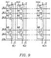
- a memory cell array with NAND structured cells has a plurality of NAND cell units arranged in a matrix with columns and rows.
- Fig. 9 is an equivalent circuit diagram showing a part of the memory cell array with conventional NAND structured cells.
- each of the NAND cell units NU1 to NUm has a first selection transistor 120 with its drain connected to the corresponding bit line and a second selection transistor 121 with its source connected to a common source line CSL.
- the drain-source channels of memory cell transistors M1 to M8 (hereinafter referred to as "memory cells”) are serially connected between a source of the first selection transistor 120 and a drain of the second selection transistor 121.
- the gates of the first selection transistors 120, the control gates of the memory cells M1 to M8 and the gates of the second selection transistors 121 are connected to a first selection line SL1, word lines WL1 to WL8 and a second selection line SL2, respectively.
- the first and second selection transistors 120 and 121 and the memory cells M1 to M8 are formed in the P type well formed on the main surface of a semiconductor substrate.
- the source-drain common region between the source of the first selection transistor 120 and the drain of the memory cell M1, the source-drain common regions of the memory cells M1 to M8, and the drain-source common region between the drain of the second selection transistor 121 and the source of the memory cell M8 are formed in the P type well.
- a floating gate made of polysilicon is formed on each channel of the memory cells M1 to M8 through a tunnel oxide layer, and a floating gate made of polysilicon or of metal silicide with a high melting point is formed thereon through an intermediate insulating layer.
- the drain regions of the first selection transistors 120 formed in the P type well are respectively connected to the corresponding bit lines made of metal silicide or metal through openings, the source regions of the second selection transistors 121 formed in the P type well are connected to the common source line CSL made of the metal silicide or metal.
- the erase operation for the memory cells is performed before programming, i.e., writing data.
- the erase operation for the memory cells is performed by applying an erase voltage of about 20 V to the P type well region and reference a voltage, i.e., ground voltage to the word lines WL1 to WL8. With the electrons stored in the floating gates being emitted to the P type well region through the tunnel oxide layer, the memory cells are changed to enhancement mode transistors. It can be assumed that the erased memory cells store the data "1".
- the programming operation for the memory cells connected to the selected word line i.e., the writing operation of the data "0" is performed by applying a program voltage of about 18 V to the selected word line and the reference voltage, i.e., the ground voltage Vss to the sources and drains of the memory cells in which the data "0" is written. Then, the floating gates of the memory cells to be programmed accumulate electrons through the tunnel oxide layers, and these memory cells are changed to depletion mode transistors.
- the program verification operation is performed to verify whether or not the selected memory cells are successfully programmed to have a predetermined constant threshold voltage value.
- the size of the memory cell such as the width and thickness of the gate oxide layer and the width and length of the channel region, has been reduced.
- variance of the manufacturing process cannot secure the uniformity of the width and thickness of the gate oxide layer, intermediate the insulating layer and channel region.
- a program verification device has been proposed for verifying whether or not the selected memory cells are successfully programmed.
- such a program verification technique is disclosed in the aforementioned Korean Patent Publication No. 94-18870.
- the threshold voltages of the programmed memory cells are still unequal.
- the variance of the circumstances and conditions such as power supply voltage or operating temperature may deteriorate the reliability of the EEPROM.
- Patent Abstract vol.11, no.216 (P-595) of JP 62 033 397 describes a circuit according to the preamble of claim 1.
- IBM Technical disclosure Bulletin , November 1984, US, Vol-27, NR-6, PG - 3302-3307 discloses a memory device similar to those described above.
- US patent 5,175,706 describes a ramp generator, and a combined ramp generator and voltage reference, for gradually applying a predetermined programming voltage to selected memory cells.
- the present invention provides an auto-program voltage generator for use in a non-volatile semiconductor memory having a plurality of memory cells and means for performing repeated sequential program and program verification operations on selected memory cells until the selected memory cells are successfully programmed.
- the auto-program voltage generator comprises means for generating a program voltage which sequentially increases after unsuccessful program operations on the selected memory cells, and comprises: a high voltage generator for generating a program voltage; and a himming circuit for adjusting the level of the program voltage to increase sequentially the program voltage within a predetermined voltage range every time the selected memory cells are not successfully programmed.
- the trimming circuit comprises: a first resistive element connected between a common node and a ground node; a second resistive element connected between the common node and a program voltage output of the high voltage generator, means for varying a resistance of the first resistive element; and means for maintaining a potential difference between the ground voltage and the common node at a fixed, predetermined value by adjusting the program voltage.
- a plurality of controllable bypass means are preferably each connected between the ground node and a respective node between a respective pair of adjacent sub-elements for selectively short-circuiting selected ones of the resistive sub-elements.
- the ground node is connected to the ground voltage only when programming is being carried out.
- the means for varying the resistance may comprise means for activating a selected one of the bypass means.
- the first and second resistive elements may comprise a plurality of resistors serially connected between a program voltage generation terminal of the high voltage generator and a reference voltage.
- the bypass means may comprise a plurality of transistors for respectively bypassing selected ones of the said plurality of resistors to increase sequentially the program voltage.
- a trimming signal generator may be connected to control each of the said plurality of bypass means, for increasing sequentially the program voltage.
- the trimming signal generator may comprise latch means for generating a constant voltage after the program voltage has been sequentially increased. Any such auto-program voltage generator may further comprise a binary counter connected to the trimming signal generator, for sequentially activating the plurality of bypass means.
- a loop counting circuit may be provided, for stopping the generation of the program voltage in response to counting signals output from the binary counter.
- the present invention provides a method of programming a non-volatile semiconductor memory having a plurality of memory cells comprising sequentially performing program and program verification operations on selected memory cells until the selected memory cells are successfully programmed.
- the program voltage is increased each time the selected memory cells are not successfully programmed.
- the method comprises: (a) generating a program voltage in a high voltage generator; (b) passing a current through a series connection of: a first resistive element connected between a common node and a ground voltage; and a second resistive element connected between the common node and a program voltage output; (c) comparing the level of a voltage at the common node with a reference voltage; (d) generating a comparing signal according to the result of the comparison of step (c); (e) activating the high voltage generator in response to the comparing signal, to adjust the program voltage such that the common node voltage level is substantially equal to the reference voltage; and (f) sequentially increasing the program voltage within a predetermined voltage range every time the selected memory cells are not successfully programmed, by sequentially reducing the resistance of the first resistive element, and repeating steps (b)-(e).
- the first resistive element may comprise a series-connected plurality of resistive sub-elements, and wherein the resistance of the first resistive element is varied by selectively short-circuiting selected ones of the resistive sub-elements.
- a plurality of controllable bypass means may each be connected between a ground node and a respective node between a respective pair of adjacent sub-elements for selectively short-circuiting selected ones of the resistive sub-elements.
- the resistance of the first resistive element may be sequentially reduced by selectively activating one of the bypass means.
- the program voltage is sequentially increased within a predetermined voltage range and then maintains a constant voltage level.
- the constant voltage level is preferably set to prevent the junction break down and the break down of the gate oxide layer of memory cells.
- the predetermined voltage range may be about from 15V to 19.5V.
- the present invention further provides a non-volatile semiconductor memory having a plurality of memory cells, means for performing sequential program and program verification operations on selected memory cells until the selected memory cells are successfully programmed, and an auto-program voltage generator as described.
- the memory comprises: a plurality of NAND cell units arranged in a memory cell array in a matrix with columns and rows, each NAND cell unit having a plurality of the said memory cells having their channels serially connected to one another, each memory cell-being a floating gate type transistor with a floating gate and a control gate, and including a plurality of word lines connected to the control gates of the said memory cells arranged in the same column; program means for programming predetermined memory cells of the cells connected to a selected word line and program verification means for verifying whether or not the said predetermined memory cells are successfully programmed; and a pass voltage generator for providing to unselected word lines a pass voltage which increases sequentially while maintaining a predetermined voltage difference as compared with the sequentially increasing program voltage.
- the pass voltage generator comprises a voltage generator for generating a pass voltage; and a trimming circuit for adjusting the level of the pass voltage to increase sequentially the pass voltage within a predetermined voltage range every time the selected memory cells are not successfully programmed.
- the trimming circuit preferably comprises a first resistive element connected between a common node and a ground node; a second resistive element connected between the common node and a pass voltage output of the voltage generator, means for varying a resistance of the first resistive element; and means for maintaining a potential difference between the ground voltage and the common node at a fixed, predetermined value.
- N-channel transistors of depletion mode (hereinafter referred to as "D type transistors") having a threshold voltage of -1.8V
- N type transistors of enhancement mode (hereinafter referred to as “N type transistors”) having a threshold voltage of 0.7V
- P type transistors P-channel MOS transistors
- Fig. 1 illustrates a program voltage generator 200.
- a high voltage generator 10 functions to generate a program voltage Vpgm in response to a charge pumping signal ⁇ pp and its complementary signal ⁇ pp output from a high voltage generation control circuit 20.
- the high voltage generator 10 is a well-known circuit for generating a program voltage Vpgm higher than the power supply voltage Vcc by utilizing a charge pumping method.
- the high voltage generator 10 comprises an N type transistor 17 providing an initial voltage Vcc-Vth to a node 1, N type transistors 11 to 16 having their own channels serially connected between the node 1 and an output node 2, and MOS capacitors 3 to 8 respectively connected to the gates of the N type transistors 11 to 16.
- the gates of the N type transistors 11 to 16 are respectively connected to their drains.
- the drain-source common nodes of odd MOS capacitors 3, 5, and 7 and the drain-source common nodes of even MOS capacitors 4, 6, and 8 are connected to the charge pumping signal ⁇ pp and its complementary signal ⁇ pp, respectively.
- the channels of the D type transistors 18 and 19 are serially connected between the output node 2 of the high voltage generator 10 and the power supply voltage Vcc, and the gates thereof are respectively connected to a program control signal PGM and the power supply voltage Vcc.
- the D type transistors 18 and 19 function to discharge the program voltage Vpgm to the power supply voltage Vcc.
- a trimming circuit 30 for sequentially increasing the program voltage Vpgm during the program operation is connected to the output node 2.
- the trimming circuit 30 in which the channel of an N type transistor 31 and the resistors R 1 to R 10 , R n and R m are serially connected to one another and the gate of the N type transistor 31 is connected to the program control signal PGM through an inverter 32.
- a connection node 37 between the resistors R n and R 10 is connected to a connection node 38 between the resistor R 1 and the drain of the N type transistor 31 through the channel of an N type transistor 33.
- the connection nodes between the resistors R 10 to R 1 are respectively connected to the connection node 38 through the channels of the transistors 34 and 35.
- the gates of the transistors 33 to 35 are respectively connected to the trimming signals TRM P1 to TRM P10 .
- the transistors 33 to 35 are bypass means for bypassing the resistors R 1 to R 10 , sequentially.
- a comparing circuit 40 functions to compare the reference voltage Vpref with the voltage V 36 of the connection node 36 between the resistors R m and R n .
- the channel of a transistor 41 is connected between the ground voltage Vss and a common node 46, and the gate thereof is connected to the program control signal PGM through an inverter 47.
- a first branch in which the channels of the P type transistor 44 and N type transistor 42 are serially connected and a second branch in which the channels of the P type transistor 45 and N type transistor 43 are serially connected are connected in parallel between the power supply voltage Vcc and the common node 46.
- the gates of the P type transistors 44 and 45 are commonly connected to each other and are also connected to a connection node 48 between the P type transistor 45 and the N type transistor 43.
- the reference voltage Vpref i.e., about 1.67V is applied to the gate of the N type transistor 43.
- the gate of the N type transistor 42 is connected to the common node 36.
- the connection node 49 between the P type transistor 44 and the N type transistor 42 serves as an output terminal of the comparing circuit 40.
- the comparing circuit 40 outputs the logic "low” state if the voltage V 36 > the reference voltage Vpref, and outputs the logic "high” state if V 36 ⁇ Vpref.
- the high voltage generation control circuit 20 is connected between the comparing circuit 40 and the high voltage generator 10 and functions to control the program voltage Vpgm to maintain a predetermined constant voltage level.
- the high voltage generation control circuit 20 comprises a NAND gate 22 having one input connected to the connection node 49 and the other connected to the program control signal PGM through an inverter 21.
- the first inputs of the NAND gates 24 and 25 receive the output of the NAND gate 22 through an inverter 23, and the second inputs thereof respectively receive the clock pulses ⁇ p and ⁇ p from a ring oscillator (not shown). At this time, the clock pulses ⁇ p and ⁇ p have a frequency of about 8MHz.
- the NAND gates 24 and 25 output the charge pumping signals ⁇ pp and ⁇ pp through inverters 26 and 27.
- V 36 > Vpref the high voltage generation control circuit 20 is inactivated, and if V 36 ⁇ Vpref, it becomes activated.
- the program voltage Vpgm increases, the voltage V 36 also increases. Therefore, the high voltage generation control circuit 20 is inactivated and thus the high voltage generator 10 reduces the program voltage Vpgm.
- the program voltage Vpgm is reduced, the high voltage generator 10 increases the program voltage Vpgm.
- the program voltage Vpgm maintains a constant voltage level by the control of the high voltage generation control circuit 20.
- Vpgmin Vpref (1+ R m R 1 +R 2 +.... +R 10 +R n )
- V pgm1 Vpref (1 + R m R 2 +.... +R 10 +R n )
- V pgm2 Vpref (1+ R m R 3 +.... +R 10 +R n )
- the program voltage on the output node 2 is sequentially increased. Accordingly, by sequentially performing the program and program verification operations while increasing the program voltage sequentially within a predetermined voltage range, i.e., from 15V to 19.5V, the memory cells having constant threshold voltages regardless of various changes such as process changes and the changes in conditions can be implemented.
- Fig. 2 is a trimming signal generator 300 for generating trimming signals which sequentially increase the program voltage Vpgm by sequentially turning on the transistors 35 to 33 in Fig. 1.
- the trimming signal generator 300 has a plurality of NOR gates 51 to 55 which receive the combinations of the output signals LP 1 to LP 4 of a binary counter and their complementary signals LP 1 to LP 4 .
- the output of the NOR gate 55 is coupled to one input of a NOR gate 56 in a flip-flop.
- the output of the NOR gate 56 is applied to the NOR gates 51 to 55 through an inverter 58, and also to one input of a NOR gate 57.
- the other input of the NOR gate 57 in the flip-flop is coupled to the program control signal PGM , and the output thereof is connected to the trimming signal TRM P10 and also to the other input of the NOR gate 56.
- the flip-flop composed of the NOR gates 56 and 57 latches the trimming signal TRM P10 to the logic "high” state if the NOR gate 55 is selected, i.e., the NOR gate 55 outputs the logic "high” state.
- the inverter 58 provides the output of the NOR gate 56 as a feedback signal.
- the NOR gates 56 and 57 and the inverter 58 are latch means for latching the trimming signals TRM P1 to TRM P10 to the logic "low" state. Therefore, if the selected memory cell is not successfully programmed even after the completion of the tenth program verification operation, the program operations thereafter maintain the increased maximum program voltage Vpgmmax level, i.e., 19.5V according to the preferred embodiment of the present invention.
- Vpgmmax is selected as the value capable of preventing the junction break down and the break down of the gate oxide layer of the memory cell
- the present invention is not limited to the maximum program voltage level of 19.5V.
- the present invention employs 10 trimming signals, however, it is not limited thereto, either. However, it is desired that the program voltage increment ⁇ V by which it is increased every program operation should be below 1V, preferably below 0.5V.
- Fig. 3A shows the binary counter and Fig. 3B a schematic circuit diagram of each stage in the binary counter of Fig. 3A.
- the channels of N type transistors 65 to 68 are serially connected between an output terminal Oi+1 and its complementary output terminal O i+1, the gates of the transistors 66 and 67 are commonly connected to a complementary clock input terminal O i, and the gates of the transistors 65 and 68 to the clock input terminal Oi.
- An inverter 64 is connected between the output terminal Oi+1 and its complementary output terminal O i+1.
- a second input of a NAND gate 61 is coupled to a connection node between the transistors 65 and 66, and the output thereof to a connection node between the transistors 66 and 67 through an inverter 63.
- a second input of the NAND gate 62 is coupled to a connection node between the transistors 67 and 68, and the output thereof to the complementary output terminal O i+1.
- the binary counter 400 of Fig. 3A is composed of 7 stages serially connected one another.
- the reset terminal R is coupled to the reset signal RST , and the clock input terminal Oi and its complementary clock input terminal O i at the first stage are respectively connected to the clock signal CK and its complementary clock signal CK .
- the 7 stages 71 to 77 output complementary counting signals LP 1 to LP 7
- the 4 stages 71 to 74 output the counting signals LP 1 to LP 4 . Every time the clock signal CK goes to the logic "low" state, the counting signals LP 1 to LP 4 are counted up and the complementary counting signals LP 1 to LP 7 are counted down.
- Fig. 4 is a circuit diagram showing a clock signal generator for generating the clock signal to be provided to the binary counter 400 of Fig. 3A.
- a program and verification signal PGMs is generated from a timer (not shown) in response to the program control signal PGM .
- the clock signal generator comprises a short pulse generator 80 composed of inverters 81 to 83 and a NAND gate 84, inverters 85 to 88, and NOR gates 89 and 90.
- the NOR gates 89 and 90 are comprised in a flip-flop.
- the short pulse generator 80 generates the short pulse of logic "low” state when the program and verification signal PGMs goes to the logic "high” state.
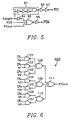
- Fig. 5 is a schematic circuit diagram of a control signal generator for generating the reset signal RST and the program control signal PGM .
- the control signal generator of Fig. 5 generates the reset signal RST through a short pulse generator 91 and inverters 92 and 93 in response to an auto-program flag signal Sapgm outputted from a command register (not shown).
- the auto-program flag signal Sapgm is applied to a first input of a NOR gate 95 through an inverter 94, a program detection signal PDS to a second input thereof and a loop counting signal PCout to a third input thereof.
- the NOR gate 95 outputs the program control signal PGM through an inverter 96.
- the program detection signal PDS is generated according to the program verification operation.
- the program detection signal PDS becomes the logic "high” state. On the contrary, if at least one of the selected memory cells has not been successfully programmed, the program detection signal PDS becomes the logic "low” state.
- Such a program verification technique is disclosed in the aforementioned Korean Patent Publication No. 94-18870.
- Fig. 6 shows a loop counting circuit 500 for generating the loop counting signal PCout.
- the loop counting circuit 500 is a logic circuit composed of NAND gates 101 to 110 and a NOR gate 111.
- the complementary counting signals LP 1 to LP 7 are applied from the binary counter 400 to the NAND gates 101 to 107, respectively.
- the terminals N0 to N6 are connected to the ground voltage Vss or to the power supply voltage Vcc according to the loop counting frequency.
- the loop counting frequency is set to 20 according to the preferred embodiment of the present invention, the terminals N2 and N5 are connected to the power supply voltage Vcc, and the remaining terminals N0, N1, N3, N4, and N6 are connected to the ground voltage Vss.
- the auto-program operation starts in response to the transition of the auto-program flag signal Sapgm from the logic “low” state to the logic "high” state.
- the control signal generator generates a program control signal PGM of logic "low” state in response to the transition of the auto-program flag signal Sapgm from the logic "low” state to the logic "high” state.
- the short pulse generator 91 in response to the auto-program flag signal Sapgm which goes to the logic "high” state, the short pulse generator 91 generates the short pulse of logic "low” state and thereby the binary counter 400 of Fig. 3A is reset.
- the timer (not shown) generates the program and verification signal pGMs in response to the transition of the program control signal from the logic "high” state to the logic "low” state.
- the program and verification signal PGMs is the clock pulse which has the logic “low” state of 30 ⁇ sec and the logic "high” state of 10 ⁇ sec when the program control signal PGM is in the logic "low” state.
- the duration when the program control signal remains in the logic “low” state is for the program operation, and the duration when the program control signal remains the logic "high” state is for the program verification operation.
- the program voltage generator 200 of Fig. 1 is enabled. That is, the transistor 41 is turned on, thus activating the comparing circuit 40, and the transistor 31 is turned on, thus activating the trimming circuit 30.
- the comparing circuit 40 outputs the logic "high” state.
- the inverter 23 outputs the logic "high” state and thereby the high voltage generation control circuit 20 generates the charge pumping signal ⁇ pp and its complementary signal ⁇ pp.
- the high voltage generator 10 generates the gradually increasing high voltage by the signals ⁇ pp and ⁇ pp.
- the program voltage Vpgm increases until the voltage V 36 at the connection node 36 reaches the reference voltage Vpref. Consequentially, the program voltage Vpgm maintains the initial program voltage Vpgmin shown in the above-described equation (1).
- the technique for programming the selected memory cells with the program voltage Vpgm is disclosed in the Korean Patent Publication No. 94-18870.
- the program and verification signal PGMs goes to the logic "high” state, and the program verification operation for the programmed memory cells is performed during the time between t 1 and t 2 .
- the short pulse generator 80 of Fig. 4 In response to the program and verification signal PGMs which goes to the logic "high” state at time t 2 , the short pulse generator 80 of Fig. 4 generates the short pulse and the inverter 86 generates the short pulse signal ⁇ sp of logic "low” state.
- the clock signal CK is generated as a similar signal to the short pulse signal ⁇ sp.
- the binary counter 400 of Fig. 3A makes the counting signal LP 1 the logic "high” state as shown in Fig. 7. Thereby, the NOR gate 51 of Fig.
- a reprogram operation is automatically performed with the increased program voltage V pgm1 during the time between t 3 and t 4 .
- the short pulse generator 80 of Fig. 4 generates the short pulse of logic "low” state, and the inverter 86 outputs the short pulse ⁇ sp of logic "low” state as shown in Fig. 7.
- the clock signal CK becomes the short pulse of logic "low” state, and the counting signals LP 1 and LP 2 of the binary counter 400 become the logic "low” and logic “high” states, respectively.
- the NOR gate 52 of Fig. 2 generates the trimming signal TRM P2 which goes to the logic "high” state.
- the high voltage generation control circuit 20 is activated, and thereby the high voltage generator 10 generates the program voltage V pgm2 as shown in the above equation (3).
- the program operation is performed again during the time between t 5 and t 6 .
- the program and program verification operations are automatically performed until all the selected memory cells are successfully programmed.
- the timing diagram of Fig. 7 shows the case that the selected memory cells are successfully programmed at the fifth program operation.
- the program detection signal PDS indicating that the selected memory cells have been successfully programmed goes to the logic "high” state at the program verification operation between the time t 10 and t 11 .
- the control signal generator of Fig. 5 makes the program control signal PGM logic "high” state, and the circuits related to the program like a ring counter (not shown) are inactivated.
- the auto-program flag signal Sapgm becomes the logic "low” state. It is possible to detect how many program loops have occurred during the 2.5 ⁇ sec with the complementary counting signals LP 1 to LP 7 outputted from the binary counter 400.
- Fig. 8 is a diagram showing the relation between the program loop and the program voltage according to the preferred embodiment of the present invention.
- the program operations for the selected memory cells can be performed as much as 20 times.
- the program voltage Vpgm sequentially increases from 15V to 19.5V by 0.5V until the tenth program operation.
- the program voltage Vpgm maintains the maximum constant voltage level Vpgmmax of 19.5V by the latch operation of the flip-flop composed of the NOR gates 56 and 57.
- the loop counting circuit 500 of Fig. 6 generates the loop counting signal PCout which goes to the logic "high” state, and thereby the control signal generator of Fig. 5 generates the program control signal PGM which goes to the logic "high” state, thus stopping the generation of the program voltage Vpgm.
- the ground voltage Vss is applied to the bit line BL2 related to the memory cell M2 which is to be programmed as the data "0" within the NAND cell unit NU2
- the power supply voltage Vcc of 5V is applied to the bit line BL1 related to the memory cell M2 which should be kept the erase state, i.e., the data "1" within the NAND cell unit NU1.
- the first selection transistor 120 within the NAND cell unit NU2 is turned on and thereby the memory cell M2 within the NAND cell unit NU2 is programmed as the data "0".
- the source of the first selection transistor 120 is charged with the pass voltage Vpass, and thereby the first selection transistor 120 is turned off.
- the memory cell M2 within the NAND cell unit NU1 receives the voltage stress of 9.5V and the thin tunnel oxide layer due to the variance of the manufacturing process or the intermediate insulating layer may be broken down. Meanwhile, the threshold voltage of the memory cell M2 within the NAND cell unit NU2 is varied. Therefore, the application of the constant pass voltage Vpass to the unselected word lines deteriorates the reliability of the EEPROM. To solve this problem, the preferred embodiment of the present invention will be described with reference to Figs. 10 to 12.
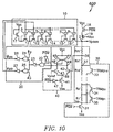
- Fig. 10 shows a pass voltage generator for generating the pass voltage to be applied to the unselected word lines.
- the pass voltage generator 600 has the same structure as the program voltage generator 200 of Fig. 1 except that the values of the resistors R 1 ' to R 10 ', R n ' and R m ' in the pass voltage generator 600 are different from those of the resistors R 1 to R 10 , R n and R m in the program voltage generator 200, and that the pass voltage Vpass instead of the program voltage Vpgm is outputted from the output node 2.
- the control signal generators shown in Figs. 2 to 6 are also employed to control the pass voltage generator 600.
- the pass voltage generator 600 generates the pass voltage Vpass which increases sequentially from the initial pass voltage Vpassin of 8V to the maximum pass voltage Vpassmax of 12.5V according to the program loop.
- the generation of the increasing pass voltage Vpass can be implemented by using the proper values of the resistors R 1 ' to R 10 ', R n and R m .
- the operations of the pass voltage generator 600 are identical to those of the program voltage generator 200 except the value of the pass voltage Vpass, and such will not be described.
- the control signal generators shown in Figs. 2 to 6 are employed in the pass voltage generator 600 of Fig. 10, and such will not be described, either.
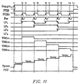
- Fig. 11 is a timing diagram for describing the operations of the pass voltage generator of Fig. 10.
- Fig. 11 is identical to Fig. 7 except that the pass voltage Vpass is generated instead of the program voltage Vpgm.
- Fig. 12 is a diagram showing the relation between the program voltage Vpgm and the pass voltage Vpass according to the program loop. As can be seen in the figure, the voltage difference between the program voltage Vpgm and the pass voltage Vpass maintains 5V until the tenth program operation. Such a voltage difference can be set properly according to the structure or properties of the memory cells to prevent the insulation break down or the variance of the threshold voltage of the memory cells which should not be programmed.
- the auto-program voltage generator and the pass voltage generator according to the present invention generate program and pass voltages which increase sequentially within a predetermined voltage range, the reliability of the chip can be enhanced without breakdown of the insulating layer or variance of the threshold voltage of the memory cells which should not be programmed. In addition, it is possible to achieve uniform threshold voltages, and to enhance the performance of the chip regardless of process variations and variations in conditions.
Landscapes
- Read Only Memory (AREA)
- For Increasing The Reliability Of Semiconductor Memories (AREA)
Claims (17)
- Selbstprogrammier-Spannungsgenerator (200) zur Verwendung in einem nicht-flüchtigen Halbleiterspeicher, der eine Vielzahl von Speicherzellen (M) und Mittel zur Ausführung von wiederholten, aufeinanderfolgenden Programmier- und Programmverifikationsoperationen auf ausgewählten Speicherzellen bis die ausgewählten Speicherzellen erfolgreich programmiert sind aufweist, wobei der Selbstprogrammier-Spannungsgenerator Mittel zur Erzeugung einer Programmierspannung aufweist, die sich nach erfolglosen Programmieroperationen auf den ausgewählten Speicherzellen schrittweise erhöht, wobei der Selbstprogrammier-Spannungsgenerator aufweist:wobei die Trimmschaltung aufweist:einen Hochspannungsgenerator (10) zur Erzeugung einer Programmierspannung (Vpgm);eine Trimmschaltung (30) zur Einstellung des Pegels der Programmierspannung, um die Programmierspannung schrittweise (TRMp1-TRMp10; 33-35) innerhalb eines vorbestimmten Spannungsbereiches jedes Mal zu erhöhen, wenn die ausgewählten Speicherzellen nicht erfolgreich programmiert werden;dadurch gekennzeichnet, daß sie auchein erstes Widerstandselement (Rn, R1-R10), das zwischen einen gemeinsamen Knoten (36) und einen Erdungsknoten (38) geschaltet ist;ein zweites Widerstandselement (Rm), das zwischen den gemeinsamen Knoten und einen Programmierspannungsausgang (Vpgm) des Hochspannungsgenerators geschaltet ist;Mittel (33-35) zur Änderung des Widerstandes des ersten Widerstandselementes; undMittel (40, 20, 10) aufweist, um eine Potentialdifferenz (V36) zwischen der Erdspannung und dem gemeinsamen Knoten durch Anpassung der Programmierspannung auf einem festen, vorbestimmten Wert (Vpref) zu halten.
- Selbstprogrammier-Spannungsgenerator nach Anspruch 1, wobei das erste Widerstandselement in Reihenschaltung eine Vielzahl von Teilwiderstandselementen (R1-R10) aufweist, und wobei der Widerstand des ersten Widerstandselementes durch selektives Kurzschließen (TRMp) von ausgewählten Teilwiderstandselementen verändert wird.
- Selbstprogrammier-Spannungsgenerator nach Anspruch 2, wobei eine Vielzahl von steuerbaren Überbrückungsmitteln (33-35) jeweils zwischen den Erdungsknoten (38) und einen jeweiligen Knoten zwischen einem jeweiligen Paar von direkt benachbarten Teilelementen geschaltet ist, um ausgewählte Teilwiderstandselemente selektiv kurzzuschließen.
- Selbstprogrammier-Spannungsgenerator nach einem der Ansprüche 1-3, wobei der Erdungsknoten (38) mit der Erdspannung (Vss) nur dann verbunden ist, wenn die Programmierung durchgeführt wird.
- Selbstprogrammier-Spannungsgenerator nach Anspruch 3 oder 4, wobei die Mittel zur Änderung des Widerstandes Mittel zur Aktivierung eines ausgewählten Überbrückungsmittels aufweisen.
- Selbstprogrammier-Spannungsgenerator nach einem der Ansprüche 3-5, wobei das erste und zweite Widerstandelement eine Vielzahl von Widerständen (Rm-R1), die in Reihe zwischen einen Programmierspannungserzeugungsanschluß (2) des Hochspannungsgenerators und eine Referenzspannung (38; Vss) geschaltet sind, und die Überbrückungsmittel eine Vielzahl von Transistoren zur jeweiligen Überbrückung von ausgewählten aus der Vielzahl der Widerstände aufweisen, um die Programmierspannung schrittweise zu erhöhen.
- Selbstprogrammier-Spannungsgenerator nach Anspruch 5 oder 6, der außerdem einen Trimmsignalgenerator (300) aufweist, der angeschlossen ist, um jedes aus der Vielzahl der Überbrückungsmittel zu steuern, um die Programmierspannung schrittweise zu erhöhen.
- Selbstprogrammier-Spannungsgenerator nach Anspruch 7, wobei der Trimmsignalgenerator Haltemittel (56-58) aufweist, um eine konstante Spannung zu erzeugen, nachdem die Programmierspannung schrittweise erhöht worden ist.
- Selbstprogrammier-Spannungsgenerator nach Anspruch 7 oder 8, der außerdem einen binären Zähler (400) aufweist, der mit dem Trimmsignalgenerator verbunden ist, um die Vielzahl von Überbrückungsmitteln nacheinander zu aktivieren.
- Selbstprogrammier-Spannungsgenerator nach Anspruch 9, der außerdem eine Schleifenzählerschaltung (500) zum Beenden der Erzeugung der Programmierspannung in Reaktion auf von dem binären Zähler ausgegebene Zählsignale aufweist.
- Verfahren zur Programmierung eines nicht-flüchtigen Halbleiterspeichers, der eine Vielzahl von Speicherzellen (M) hat, das die aufeinanderfolgende Ausführung von Programmier- und Programmverifikationsoperationen auf ausgewählten Speicherzellen bis die ausgewählten Speicherzellen erfolgreich programmiert sind umfaßt, und bei dem die Programmierspannung jedes Mal erhöht wird, wenn die ausgewählten Speicherzellen nicht erfolgreich programmiert werden, wobei das Verfahren umfaßt:(a) Erzeugung einer Programmierspannung (Vpgm) in einem Hochspannungsgenerator (10);(b) Durchleiten eines Stroms durch eine Reihenschaltung aus:gekennzeichnet durch:einem ersten Widerstandselement (Rn, R1-R10), das zwischen einen gemeinsamen Knoten (36) und eine Erdspannung (Vss) geschaltet ist; undein zweites Widerstandselement (rm), das zwischen den gemeinsamen Knoten und einen Programmierspannungsausgang (Vpgm) geschaltet ist;(c) Vergleich des Pegels einer Spannung (V36) an dem gemeinsamen Knoten (36) mit einer Referenzspannung (Vpref);(d) Erzeugung eines Vergleichssignals (4) entsprechend dem Ergebnis des Vergleichs von Schritt (c);(e) Aktivierung des Hochspannungsgenerators in Reaktion auf das Vergleichssignal, um die Programmierspannung so einzustellen, daß der Spannungspegel (V36) des gemeinsamen Knotens im wesentlichen gleich der Referenzspannung ist; und(f) schrittweise Erhöhung (TRMp1-TRMp10; 33-35) der Programmierspannung innerhalb eines vorbestimmten Spannungsbereiches jedes Mal, wenn die ausgewählten Speicherzellen nicht erfolgreich programmiert werden, durch schrittweise Erniedrigung des Widerstandes des ersten Widerstandselementes und Wiederholung der Schritte (b)-(e).
- Verfahren nach Anspruch 11, wobei das erste Widerstandselement in Reihenschaltung eine Vielzahl von Teilwiderstandselementen (R1-R10) aufweist, und wobei der Widerstand des ersten Widerstandselementes durch selektives Kurzschließen (TRMp) von ausgewählten Teilwiderstandselementen verändert wird.
- Verfahren nach Anspruch 12, wobei eine Vielzahl von steuerbaren Überbrückungsmitteln (TRMp1-TRMp10) jeweils zwischen den Erdungsknoten (38) und einen jeweiligen Knoten zwischen einem jeweiligen Paar von direkt benachbarten Teilelementen geschaltet wird, um ausgewählte Teilwiderstandselemente selektiv kurzzuschließen (TRMp).
- Verfahren nach Anspruch 12 oder 13, wobei der Widerstand des ersten Widerstandselementes durch selektive Aktivierung von einem der Überbrückungsmittel schrittweise erniedrigt wird.
- Verfahren nach einem der Ansprüche 11-14, wobei die Programmierspannung innerhalb eines vorbestimmten Spannungsbereichs schrittweise erhöht wird und dann einen konstanten Spannungspegel hält.
- Verfahren nach Anspruch 15, wobei der konstante Spannungspegel eingestellt ist, um den Grenzschichtdurchbruch und den Durchbruch der Gate-Oxidschicht der Speicherzellen zu verhindern.
- Verfahren nach Anspruch 15 oder 16, wobei der vorbestimmte Spannungsbereich ungefähr zwischen 15V und 19.5V liegt.
Applications Claiming Priority (4)
| Application Number | Priority Date | Filing Date | Title |
|---|---|---|---|
| KR19940022769 | 1994-09-09 | ||
| KR9422769 | 1994-09-09 | ||
| KR1019950001144A KR0142368B1 (ko) | 1994-09-09 | 1995-01-24 | 불휘발성 반도체 메모리장치의 자동프로그램 회로 |
| KR9501144 | 1995-01-24 |
Publications (3)
| Publication Number | Publication Date |
|---|---|
| EP0701259A2 EP0701259A2 (de) | 1996-03-13 |
| EP0701259A3 EP0701259A3 (de) | 1998-09-23 |
| EP0701259B1 true EP0701259B1 (de) | 2001-12-12 |
Family
ID=26630558
Family Applications (1)
| Application Number | Title | Priority Date | Filing Date |
|---|---|---|---|
| EP95114118A Expired - Lifetime EP0701259B1 (de) | 1994-09-09 | 1995-09-08 | Selbst-Programmierschaltung für eine nicht-flüchtige Speicheranordnung |
Country Status (6)
| Country | Link |
|---|---|
| US (1) | US5642309A (de) |
| EP (1) | EP0701259B1 (de) |
| JP (1) | JP2895779B2 (de) |
| KR (1) | KR0142368B1 (de) |
| CN (1) | CN1095171C (de) |
| DE (1) | DE69524507T2 (de) |
Families Citing this family (69)
| Publication number | Priority date | Publication date | Assignee | Title |
|---|---|---|---|---|
| DE19528476C2 (de) * | 1995-08-03 | 1997-11-27 | Deere & Co | Zusatzgewicht zur Fahrzeugballastierung |
| EP1260989A3 (de) | 1995-12-29 | 2005-11-30 | STMicroelectronics S.r.l. | Verfahren zum Verhindern von Störungen während des Löschens eines nichtflüchtigen Speichers |
| EP0782149B1 (de) * | 1995-12-29 | 2003-05-28 | STMicroelectronics S.r.l. | Anordnung zum Erzeugen und Regeln einer Gate-Spannung in einem nichtflüchtigen Speicher |
| JP3920943B2 (ja) * | 1996-05-10 | 2007-05-30 | 株式会社ルネサステクノロジ | 不揮発性半導体記憶装置 |
| TW338165B (en) * | 1996-09-09 | 1998-08-11 | Sony Co Ltd | Semiconductor nand type flash memory with incremental step pulse programming |
| JP3207768B2 (ja) * | 1996-09-30 | 2001-09-10 | 株式会社東芝 | 半導体装置 |
| FR2756411B1 (fr) * | 1996-11-28 | 1998-12-31 | Sgs Thomson Microelectronics | Procede d'effacement d'une memoire non volatile et electriquement effacable, et dispositifs associes |
| FR2756658B1 (fr) * | 1996-11-29 | 1999-01-22 | Sgs Thomson Microelectronics | Memoire electronique non volatile et son procede de gestion |
| US7023729B2 (en) | 1997-01-31 | 2006-04-04 | Renesas Technology Corp. | Microcomputer and microprocessor having flash memory operable from single external power supply |
| FR2768274B1 (fr) * | 1997-09-10 | 1999-11-05 | Sgs Thomson Microelectronics | Circuit de generation d'une haute tension de programmation ou d'effacement d'une memoire |
| JP2002150785A (ja) | 2000-11-08 | 2002-05-24 | Hitachi Ltd | 不揮発性半導体記憶装置 |
| DE10125164C1 (de) * | 2001-05-23 | 2003-01-16 | Infineon Technologies Ag | Halbleiter-Chip mit trimmbarem Oszillator |
| KR100453854B1 (ko) * | 2001-09-07 | 2004-10-20 | 삼성전자주식회사 | 향상된 프로그램 방지 특성을 갖는 불휘발성 반도체메모리 장치 및 그것의 프로그램 방법 |
| JP2003123493A (ja) * | 2001-10-12 | 2003-04-25 | Fujitsu Ltd | ソース電位を制御してプログラム動作を最適化した不揮発性メモリ |
| AU2003267123A1 (en) * | 2002-09-11 | 2004-04-30 | Atmel Corporation | Dac-based voltage regulator for flash memory array |
| US7038523B2 (en) * | 2003-10-08 | 2006-05-02 | Infineon Technologies Ag | Voltage trimming circuit |
| KR100521385B1 (ko) * | 2003-12-15 | 2005-10-12 | 삼성전자주식회사 | 고전압 발생 회로 및 그것을 포함한 반도체 메모리 장치 |
| US7161833B2 (en) | 2004-02-06 | 2007-01-09 | Sandisk Corporation | Self-boosting system for flash memory cells |
| US7466590B2 (en) | 2004-02-06 | 2008-12-16 | Sandisk Corporation | Self-boosting method for flash memory cells |
| KR100632940B1 (ko) * | 2004-05-06 | 2006-10-12 | 삼성전자주식회사 | 프로그램 사이클 시간을 가변시킬 수 있는 불 휘발성반도체 메모리 장치 |
| KR100632944B1 (ko) * | 2004-05-31 | 2006-10-12 | 삼성전자주식회사 | 동작 모드에 따라 프로그램 전압의 증가분을 가변할 수있는 불 휘발성 메모리 장치 |
| KR100626377B1 (ko) * | 2004-06-07 | 2006-09-20 | 삼성전자주식회사 | 동작 모드에 따라 프로그램 전압의 증가분을 가변할 수있는 불 휘발성 메모리 장치 |
| CN100345748C (zh) * | 2004-07-07 | 2007-10-31 | 日立住友重机械建机起重机株式会社 | 用于建筑机械的配重装置 |
| KR100560822B1 (ko) * | 2004-09-02 | 2006-03-13 | 삼성전자주식회사 | 리플-프리 내부 전압을 발생하는 반도체 장치 |
| KR100634412B1 (ko) * | 2004-09-02 | 2006-10-16 | 삼성전자주식회사 | 향상된 프로그램 특성을 갖는 불 휘발성 메모리 장치 |
| KR100632951B1 (ko) | 2004-09-22 | 2006-10-11 | 삼성전자주식회사 | 리플 안정화 기능을 갖는 고전압 발생 회로 |
| KR100645049B1 (ko) * | 2004-10-21 | 2006-11-10 | 삼성전자주식회사 | 프로그램 특성을 향상시킬 수 있는 불 휘발성 메모리 장치및 그것의 프로그램 방법 |
| KR100572332B1 (ko) * | 2004-10-26 | 2006-04-18 | 삼성전자주식회사 | 불 휘발성 메모리 장치 및 그것의 프로그램 방법 |
| KR100645054B1 (ko) | 2004-10-27 | 2006-11-10 | 삼성전자주식회사 | 기생 커패시턴스의 영향을 줄인 전압 분배 회로 및 그것을포함한 워드라인 전압 발생회로 |
| KR100645055B1 (ko) | 2004-10-28 | 2006-11-10 | 삼성전자주식회사 | 플래시 메모리 장치 및 그것의 프로그램 방법 |
| KR100645059B1 (ko) * | 2004-11-04 | 2006-11-10 | 삼성전자주식회사 | 정밀한 전압 조정을 수행하는 트리밍 회로 및 이를 구비한반도체 메모리 장치 |
| KR100748553B1 (ko) * | 2004-12-20 | 2007-08-10 | 삼성전자주식회사 | 리플-프리 고전압 발생회로 및 방법, 그리고 이를 구비한반도체 메모리 장치 |
| KR100732756B1 (ko) * | 2005-04-08 | 2007-06-27 | 주식회사 하이닉스반도체 | 전압 펌핑장치 |
| KR100621636B1 (ko) * | 2005-06-01 | 2006-09-07 | 삼성전자주식회사 | 워드 라인 전압 발생 회로 및 그것을 갖는 불 휘발성메모리 장치 |
| KR100725979B1 (ko) * | 2005-07-23 | 2007-06-08 | 삼성전자주식회사 | 비휘발성 메모리의 기입/독출 내구력 개선 장치 및 그 방법 |
| US7362615B2 (en) | 2005-12-27 | 2008-04-22 | Sandisk Corporation | Methods for active boosting to minimize capacitive coupling effect between adjacent gates of flash memory devices |
| US7436703B2 (en) | 2005-12-27 | 2008-10-14 | Sandisk Corporation | Active boosting to minimize capacitive coupling effect between adjacent gates of flash memory devices |
| EP2528096B1 (de) * | 2005-12-27 | 2016-08-31 | SanDisk Technologies LLC | Programmierverfahren einer Flash-Speichervorrichtung mit einer Verstärkerplatte |
| US7511995B2 (en) | 2006-03-30 | 2009-03-31 | Sandisk Corporation | Self-boosting system with suppression of high lateral electric fields |
| US7428165B2 (en) | 2006-03-30 | 2008-09-23 | Sandisk Corporation | Self-boosting method with suppression of high lateral electric fields |
| KR100861647B1 (ko) * | 2006-04-06 | 2008-10-02 | 주식회사 하이닉스반도체 | 낸드 플래시 메모리 소자의 채널 부스팅 전압 측정 방법 |
| CN100538888C (zh) * | 2006-05-11 | 2009-09-09 | 盛群半导体股份有限公司 | 具有省电及速度提升能力的存储单元检测电路及其方法 |
| KR100829791B1 (ko) * | 2006-10-12 | 2008-05-19 | 삼성전자주식회사 | 플래시 메모리 장치의 전압 공급 회로, 이를 포함하는 플래시 메모리 장치 및 플래시 메모리 장치의 프로그램 전압 공급 방법 |
| KR100889780B1 (ko) | 2007-04-24 | 2009-03-20 | 삼성전자주식회사 | 패스 전압 윈도우를 향상시킬 수 있는 플래시 메모리 장치및 그것의 프로그램 방법 |
| KR100890016B1 (ko) * | 2007-05-10 | 2009-03-25 | 삼성전자주식회사 | 비휘발성 메모리 장치, 그것을 포함하는 메모리 시스템 및그것의 프로그램 방법 |
| KR100884234B1 (ko) * | 2007-05-25 | 2009-02-18 | 삼성전자주식회사 | 프로그램 성능을 향상시킬 수 있는 플래시 메모리 장치 및그것의 프로그램 방법 |
| KR101321472B1 (ko) * | 2007-07-23 | 2013-10-25 | 삼성전자주식회사 | 비휘발성 메모리 장치 및 그것의 프로그램 방법 |
| KR101358752B1 (ko) * | 2007-08-06 | 2014-02-06 | 삼성전자주식회사 | 비휘발성 메모리 장치, 그것을 포함하는 메모리 시스템 및그것의 프로그램 방법 |
| JP5178167B2 (ja) | 2007-12-04 | 2013-04-10 | 株式会社東芝 | 半導体記憶装置及びそのデータ書き込み方法 |
| JP2009146467A (ja) * | 2007-12-11 | 2009-07-02 | Toshiba Corp | 半導体集積回路装置 |
| KR101347287B1 (ko) * | 2008-02-20 | 2014-01-03 | 삼성전자주식회사 | 프로그램 전압을 가변적으로 제어할 수 있는 플래쉬 메모리장치 및 그 프로그래밍 방법 |
| KR100894490B1 (ko) * | 2008-03-03 | 2009-04-22 | 주식회사 하이닉스반도체 | 반도체 메모리장치의 내부전압 생성회로 |
| JP5217848B2 (ja) * | 2008-09-29 | 2013-06-19 | ルネサスエレクトロニクス株式会社 | 不揮発性半導体記憶装置 |
| KR101495789B1 (ko) * | 2008-11-17 | 2015-02-26 | 삼성전자주식회사 | 불휘발성 메모리 장치 및 그것의 프로그램 방법 |
| US8238161B2 (en) | 2008-11-17 | 2012-08-07 | Samsung Electronics Co., Ltd. | Nonvolatile memory device |
| KR101005165B1 (ko) * | 2009-05-29 | 2011-01-04 | 주식회사 하이닉스반도체 | 전압 발생 회로 및 이를 이용한 불휘발성 메모리 장치 |
| US7995394B2 (en) * | 2009-07-30 | 2011-08-09 | Sandisk Technologies Inc. | Program voltage compensation with word line bias change to suppress charge trapping in memory |
| JP5359663B2 (ja) * | 2009-08-03 | 2013-12-04 | ソニー株式会社 | 半導体メモリデバイスおよびその動作方法 |
| JP2011198419A (ja) * | 2010-03-19 | 2011-10-06 | Toshiba Corp | 不揮発性半導体記憶装置およびその書き込み方法 |
| JP5259667B2 (ja) * | 2010-09-22 | 2013-08-07 | 株式会社東芝 | 不揮発性半導体記憶装置 |
| JP5242730B2 (ja) * | 2011-04-18 | 2013-07-24 | 株式会社東芝 | 半導体記憶装置 |
| TWI534810B (zh) | 2011-12-09 | 2016-05-21 | Toshiba Kk | Nonvolatile semiconductor memory device |
| JP5622712B2 (ja) * | 2011-12-09 | 2014-11-12 | 株式会社東芝 | 不揮発性半導体記憶装置 |
| CN102623058B (zh) * | 2012-03-26 | 2015-01-07 | 北京兆易创新科技股份有限公司 | 非易失存储器的擦除电压产生电路及方法 |
| JP6444803B2 (ja) * | 2015-05-01 | 2018-12-26 | ラピスセミコンダクタ株式会社 | 書込電圧生成回路及びメモリ装置 |
| US9715924B2 (en) * | 2015-10-22 | 2017-07-25 | Sandisk Technologies Llc | Three dimensional non-volatile memory with current sensing programming status |
| CN106816174B (zh) * | 2015-11-30 | 2021-04-09 | 紫光同芯微电子有限公司 | 一种flash存储器编程电路及其电压控制方法 |
| CN113994315A (zh) * | 2021-08-30 | 2022-01-28 | 长江存储科技有限责任公司 | 存储器及其操作方法、存储器系统 |
| US20250349325A1 (en) * | 2024-05-09 | 2025-11-13 | Silicon Storage Technology, Inc. | High voltage generation block with trimming circuit |
Family Cites Families (17)
| Publication number | Priority date | Publication date | Assignee | Title |
|---|---|---|---|---|
| JPS6224499A (ja) * | 1985-07-24 | 1987-02-02 | Mitsubishi Electric Corp | 半導体装置 |
| JPS6233397A (ja) * | 1985-08-05 | 1987-02-13 | Mitsubishi Electric Corp | 半導体装置 |
| JPS62231500A (ja) * | 1986-03-31 | 1987-10-12 | Toshiba Corp | 半導体記憶装置 |
| JPS63153799A (ja) * | 1986-08-08 | 1988-06-27 | Nec Corp | 半導体メモリ |
| JPH01112596A (ja) * | 1987-07-07 | 1989-05-01 | Seiko Instr & Electron Ltd | 不揮発性メモリの高電圧印加方法 |
| JP2635619B2 (ja) * | 1987-09-30 | 1997-07-30 | 株式会社東芝 | 不揮発性半導体記憶装置 |
| US5053990A (en) * | 1988-02-17 | 1991-10-01 | Intel Corporation | Program/erase selection for flash memory |
| US5268870A (en) * | 1988-06-08 | 1993-12-07 | Eliyahou Harari | Flash EEPROM system and intelligent programming and erasing methods therefor |
| US5175706A (en) * | 1989-12-07 | 1992-12-29 | Sgs-Thomson Microelectronics S.A. | Programming voltage generator circuit for programmable memory |
| DE4205061C2 (de) * | 1991-02-19 | 2000-04-06 | Toshiba Kawasaki Kk | Nichtflüchtige Halbleiter-Speicheranordnung |
| KR960002006B1 (ko) * | 1991-03-12 | 1996-02-09 | 가부시끼가이샤 도시바 | 2개의 기준 레벨을 사용하는 기록 검증 제어기를 갖는 전기적으로 소거 가능하고 프로그램 가능한 불휘발성 메모리 장치 |
| US5396468A (en) * | 1991-03-15 | 1995-03-07 | Sundisk Corporation | Streamlined write operation for EEPROM system |
| JP2716906B2 (ja) * | 1992-03-27 | 1998-02-18 | 株式会社東芝 | 不揮発性半導体記憶装置 |
| JPH0643952A (ja) * | 1992-07-24 | 1994-02-18 | Sony Corp | 昇圧電圧調整回路 |
| US5450341A (en) * | 1992-08-31 | 1995-09-12 | Nippon Steel Corporation | Non-volatile semiconductor memory device having memory cells, each for at least three different data writable thereinto selectively and a method of using the same |
| JP3152756B2 (ja) * | 1992-09-14 | 2001-04-03 | 株式会社東芝 | 不揮発性半導体記憶装置 |
| US5291446A (en) * | 1992-10-22 | 1994-03-01 | Advanced Micro Devices, Inc. | VPP power supply having a regulator circuit for controlling a regulated positive potential |
-
1995
- 1995-01-24 KR KR1019950001144A patent/KR0142368B1/ko not_active Expired - Fee Related
- 1995-09-07 JP JP22985095A patent/JP2895779B2/ja not_active Expired - Lifetime
- 1995-09-08 CN CN95117154A patent/CN1095171C/zh not_active Expired - Lifetime
- 1995-09-08 EP EP95114118A patent/EP0701259B1/de not_active Expired - Lifetime
- 1995-09-08 DE DE69524507T patent/DE69524507T2/de not_active Expired - Lifetime
- 1995-09-11 US US08/526,422 patent/US5642309A/en not_active Expired - Lifetime
Also Published As
| Publication number | Publication date |
|---|---|
| EP0701259A2 (de) | 1996-03-13 |
| KR0142368B1 (ko) | 1998-07-15 |
| JPH0896591A (ja) | 1996-04-12 |
| DE69524507D1 (de) | 2002-01-24 |
| CN1095171C (zh) | 2002-11-27 |
| DE69524507T2 (de) | 2002-08-08 |
| US5642309A (en) | 1997-06-24 |
| JP2895779B2 (ja) | 1999-05-24 |
| CN1139276A (zh) | 1997-01-01 |
| KR960012023A (ko) | 1996-04-20 |
| EP0701259A3 (de) | 1998-09-23 |
Similar Documents
| Publication | Publication Date | Title |
|---|---|---|
| EP0701259B1 (de) | Selbst-Programmierschaltung für eine nicht-flüchtige Speicheranordnung | |
| KR0185611B1 (ko) | 불휘발성 반도체 메모리장치의 고전압 레벨 최적화 회로 및 그 방법 | |
| US5299162A (en) | Nonvolatile semiconductor memory device and an optimizing programming method thereof | |
| US5801987A (en) | Automatic transition charge pump for nonvolatile memories | |
| US6262926B1 (en) | Nonvolatile semiconductor memory device | |
| US6031760A (en) | Semiconductor memory device and method of programming the same | |
| KR0159455B1 (ko) | 반도체 집적회로장치 | |
| US5841721A (en) | Multi-block erase and verification circuit in a nonvolatile semiconductor memory device and a method thereof | |
| KR0157342B1 (ko) | 불휘발성 반도체 메모리의 전압 센싱 방법 | |
| US5428568A (en) | Electrically erasable and programmable non-volatile memory device and a method of operating the same | |
| KR960000616B1 (ko) | 불휘발성 반도체 메모리 장치 | |
| US6807102B2 (en) | Nonvolatile semiconductor memory and its test method | |
| JP3836643B2 (ja) | 不揮発性集積回路メモリ装置とその駆動方法 | |
| US7457165B2 (en) | Non-volatile memory device and method of programming same | |
| KR100395771B1 (ko) | 불휘발성 반도체 메모리 장치 및 그것의 프로그램 방법 | |
| US20020060926A1 (en) | Flash memory device capable of preventing program disturb and method for programming the same | |
| JP2005267821A (ja) | 不揮発性半導体メモリ | |
| JP2755936B2 (ja) | ブロック単位でストレス印加可能なストレス電圧印加回路 | |
| US6031774A (en) | Internal power supply voltage generating ciruit and the method for controlling thereof | |
| JP3184366B2 (ja) | 不揮発性半導体記憶装置 | |
| JP3176011B2 (ja) | 半導体記憶装置 | |
| JP2729432B2 (ja) | 電気的に書込消去可能な半導体記憶装置 | |
| US7180790B2 (en) | Non-volatile memory device having controlled bulk voltage and method of programming same | |
| JPH1186573A (ja) | 不揮発性半導体記憶装置 | |
| KR0172417B1 (ko) | 불휘발성 반도체 메모리장치의 프로그램 및 소거전압 인가방법 및 회로 |
Legal Events
| Date | Code | Title | Description |
|---|---|---|---|
| PUAI | Public reference made under article 153(3) epc to a published international application that has entered the european phase |
Free format text: ORIGINAL CODE: 0009012 |
|
| 17P | Request for examination filed |
Effective date: 19950913 |
|
| AK | Designated contracting states |
Kind code of ref document: A2 Designated state(s): DE FR GB |
|
| PUAL | Search report despatched |
Free format text: ORIGINAL CODE: 0009013 |
|
| AK | Designated contracting states |
Kind code of ref document: A3 Designated state(s): DE FR GB |
|
| 17Q | First examination report despatched |
Effective date: 19991008 |
|
| GRAG | Despatch of communication of intention to grant |
Free format text: ORIGINAL CODE: EPIDOS AGRA |
|
| GRAG | Despatch of communication of intention to grant |
Free format text: ORIGINAL CODE: EPIDOS AGRA |
|
| GRAH | Despatch of communication of intention to grant a patent |
Free format text: ORIGINAL CODE: EPIDOS IGRA |
|
| GRAH | Despatch of communication of intention to grant a patent |
Free format text: ORIGINAL CODE: EPIDOS IGRA |
|
| GRAH | Despatch of communication of intention to grant a patent |
Free format text: ORIGINAL CODE: EPIDOS IGRA |
|
| GRAH | Despatch of communication of intention to grant a patent |
Free format text: ORIGINAL CODE: EPIDOS IGRA |
|
| GRAA | (expected) grant |
Free format text: ORIGINAL CODE: 0009210 |
|
| AK | Designated contracting states |
Kind code of ref document: B1 Designated state(s): DE FR GB |
|
| REG | Reference to a national code |
Ref country code: GB Ref legal event code: IF02 |
|
| REF | Corresponds to: |
Ref document number: 69524507 Country of ref document: DE Date of ref document: 20020124 |
|
| ET | Fr: translation filed | ||
| PLBE | No opposition filed within time limit |
Free format text: ORIGINAL CODE: 0009261 |
|
| STAA | Information on the status of an ep patent application or granted ep patent |
Free format text: STATUS: NO OPPOSITION FILED WITHIN TIME LIMIT |
|
| 26N | No opposition filed | ||
| PGFP | Annual fee paid to national office [announced via postgrant information from national office to epo] |
Ref country code: DE Payment date: 20140822 Year of fee payment: 20 |
|
| PGFP | Annual fee paid to national office [announced via postgrant information from national office to epo] |
Ref country code: GB Payment date: 20140822 Year of fee payment: 20 |
|
| PGFP | Annual fee paid to national office [announced via postgrant information from national office to epo] |
Ref country code: FR Payment date: 20140922 Year of fee payment: 20 |
|
| REG | Reference to a national code |
Ref country code: DE Ref legal event code: R071 Ref document number: 69524507 Country of ref document: DE |
|
| REG | Reference to a national code |
Ref country code: GB Ref legal event code: PE20 Expiry date: 20150907 |
|
| PG25 | Lapsed in a contracting state [announced via postgrant information from national office to epo] |
Ref country code: GB Free format text: LAPSE BECAUSE OF EXPIRATION OF PROTECTION Effective date: 20150907 |