EP0549374B1 - Nicht-flüchtiger Halbleiterspeicher - Google Patents
Nicht-flüchtiger Halbleiterspeicher Download PDFInfo
- Publication number
- EP0549374B1 EP0549374B1 EP92311829A EP92311829A EP0549374B1 EP 0549374 B1 EP0549374 B1 EP 0549374B1 EP 92311829 A EP92311829 A EP 92311829A EP 92311829 A EP92311829 A EP 92311829A EP 0549374 B1 EP0549374 B1 EP 0549374B1
- Authority
- EP
- European Patent Office
- Prior art keywords
- voltage
- source voltage
- semiconductor memory
- verify
- nonvolatile semiconductor
- Prior art date
- Legal status (The legal status is an assumption and is not a legal conclusion. Google has not performed a legal analysis and makes no representation as to the accuracy of the status listed.)
- Expired - Lifetime
Links
Images


Classifications
-
- G—PHYSICS
- G11—INFORMATION STORAGE
- G11C—STATIC STORES
- G11C16/00—Erasable programmable read-only memories
-
- G—PHYSICS
- G11—INFORMATION STORAGE
- G11C—STATIC STORES
- G11C16/00—Erasable programmable read-only memories
- G11C16/02—Erasable programmable read-only memories electrically programmable
- G11C16/06—Auxiliary circuits, e.g. for writing into memory
- G11C16/30—Power supply circuits
-
- G—PHYSICS
- G11—INFORMATION STORAGE
- G11C—STATIC STORES
- G11C16/00—Erasable programmable read-only memories
- G11C16/02—Erasable programmable read-only memories electrically programmable
- G11C16/06—Auxiliary circuits, e.g. for writing into memory
- G11C16/26—Sensing or reading circuits; Data output circuits
-
- G—PHYSICS
- G11—INFORMATION STORAGE
- G11C—STATIC STORES
- G11C29/00—Checking stores for correct operation ; Subsequent repair; Testing stores during standby or offline operation
- G11C29/04—Detection or location of defective memory elements, e.g. cell constructio details, timing of test signals
-
- G—PHYSICS
- G06—COMPUTING OR CALCULATING; COUNTING
- G06F—ELECTRIC DIGITAL DATA PROCESSING
- G06F2201/00—Indexing scheme relating to error detection, to error correction, and to monitoring
- G06F2201/81—Threshold
Definitions
- This invention relates to a nonvolatile semiconductor memory, particularly to an EPROM and an EEPROM including a nonvolatile memory circuit and, more particularly to a circuit construction of a nonvolatile semiconductor memory of the batch erasure type (hereinafter referred to as a flash memory).
- the invention further relates particularly to a circuit construction concerning a sense amplifying (S/A) circuit, supply of a supply voltage, improvement in the reliability of a writing operation, and a high speed reading operation in a nonvolatile semiconductor memory.
- S/A sense amplifying
- Fig. 8 shows diagrammatically a structure of a cell used in a flash memory.
- V G is a gate terminal, at V D a drain terminal, at V S a source terminal, at 27 a control gate CG connected to the gate terminal V G , and at 25 a floating gate FG which is controlled by the potential of the control gate CG.
- a semiconductor substrate e.g., a semiconductor substrate having P-type conductivity.
- well portions 23, 24 made of semiconductor having N-type conductivity.
- the well portion 23 forms a drain while the well portion 24 forms a source.
- Indicated at 26, 28 are insulating films.
- the write verification and erase verification are carried out so as to confirm whether the degree of writing and the degree of erasing have a sufficient margin for the read voltage, i.e., a variation range of the normal supply voltage V CC (5V ⁇ 0.5V). Generally, these verifications are carried out to confirm that an operation margin of about 0.5V to 1.0V is available for a voltage range of V CC . In this case, the verify voltage including the operation margin is 6V to 6.5V in the write verification, and 3.5V to 4V in the erase verification.
- the write verification and the erase verification can be accomplished easily if the verify voltage including the operation margin to be secured is applied to word lines (for example, word lines WL l to WL m of the flash memory shown in Fig. 1), so that the sensitivity of the S/A circuit is the same regardless of whether the voltage V CC or the verify voltage is applied as the supply voltage of the S/A circuit.
- word lines for example, word lines WL l to WL m of the flash memory shown in Fig. 1
- US4875188 discloses a flash EPROM (nonvolatile semiconductor memory) in which such write and erase verification are accomplished by applying the appropriate verify voltage to the selected word lines.
- This nonvolatile semiconductor memory may be considered to have circuitry including a matrix of nonvolatile erasable memory cells formed at intersections of word lines and bit lines, a row decoder, a column decoder, and sense amplifiers connected to the bit lines, the nonvolatile semiconductor memory further including an internal source voltage generator for connection when the memory is in use to an external power source and operable selectively to produce predetermined internal source voltages in dependence upon the voltage of the external power source, such internal source voltages being applied to the said circuitry such that it carries out predetermined operations according to the internal source voltages, one of the said predetermined internal source voltages being a predetermined verify source voltage of a level suitable for performing a preselected verify operation on one of the said memory cells.
- the internal source voltage generator is operable selectively to apply either a write verify source voltage or an erase verify source voltage to the selected word line during the write or erase verify operation, as the case may be, but is not capable of generating a normal source voltage of a level suitable for a normal reading operation.
- Fig. 9 shows a construction of a general S/A circuit used in the nonvolatile semiconductor memory such as an EPROM.
- V CC is a line of a supply voltage 5V
- V SS a line of a supply voltage 0V.
- a gate of the transistor 11 is connected to power supply line V SS
- a gate of the transistor 12 is connected to a data line (i.e., a bit line).
- a data line i.e., a bit line.
- an n-channel transistor 13 whose gate is connected to drains of the respective transistors 11, 12.
- a p-channel transistor 14 and an n-channel transistor 15 in series.
- a gate of the transistor 14 is connected to the power supply line V SS
- a gate of the transistor 15 is connected to the drains of the respective transistors 11, 12.
- An output (data output) of the S/A circuit is taken from drains of the respective transistors 14, 15.
- the transistor 15 is provided with a function of transmitting the level of the bit line to the data output line (bit line level adjustment), and the transistor 14 is provided with a function of discriminating the data of the memory cell according to the state (on/off) of the transistor 15.
- the sensitivity of the S/A circuit becomes dependent on the voltage V CC since the voltage V CC is used as a supply voltage, thus presenting the problem that an original object of the verification cannot be accomplished.
- the desired object can be accomplished if the voltage V CC is replaced by the verify voltage.
- the size, i.e., the current supplying performance of a power supply circuit for supplying the verify voltage is disadvantageously required to be increased.
- the present invention seeks to provide a nonvolatile semiconductor memory capable of solving the aforementioned various problems collectively and having high utility value and in particular an embodiment seeks to provide a nonvolatile semiconductor memory in which an S/A circuit is permitted to have the sensitivity compatible with any of a write verification and an erase verification even if a normal supply voltage is used, that is, a verification can be conducted sufficiently.
- nonvolatile semiconductor memory in which a read voltage is reduced to a low voltage so as to consume less power so that the nonvolatile semiconductor memory is capable of carrying out verification satisfactorily and assuring a stable device operation even when it is operated at a voltage obtained by reducing a supply voltage internally.
- the prior art has also the problem that, when a read mode is executed in the nonvolatile semiconductor memory such as a flash type memory, the write data and the erase data in the read mode are erroneously determined, and thereby write and erase errors are liable to occur. It is desirable to overcome such defects residing in the prior art and to provide a power supply circuit used in a nonvolatile semiconductor memory such a flash type memory, the power supply circuit being provided with a supply voltage generating function with which a plurality of different supply voltages can be generated easily.
- a nonvolatile semiconductor memory having circuitry including a matrix of nonvolatile erasable memory cells formed at intersections of word lines and bit lines, a row decoder, a column decoder, and sense amplifiers connected to the bit lines, the nonvolatile semiconductor memory further including an internal source voltage generator for connection when the memory is in use to an external power source and operable selectively to produce predetermined internal source voltages in dependence upon the voltage of the external power source, such internal source voltages being applied to the said circuitry such that it carries out predetermined operations according to the internal source voltages, one of the said predetermined internal source voltages being a predetermined verify source voltage of a level suitable for performing a preselected verify operation on one of the said memory cells; characterised in that another one of the said internal source voltages selectively producible by the internal source voltage generator is a normal source voltage of a level suitable for performing a normal reading operation on one of the said memory cells.
- the nonvolatile semiconductor memory in one preferred embodiment comprises a cell matrix including erasable nonvolatile memory cells arranged at the intersections of the plurality of word lines and the plurality of bit lines, sense amplifying (S/A) circuits having two different kinds of source voltages supplied thereto and adapted to apply sense amplification to data of the selected line in the cell matrix, and a verify source voltage supply circuit for generating the two different kinds of source voltages in accordance with a control signal for instructing a write verification or erase verification, wherein a normal source voltage and a specific verify source voltage different from the normal source voltage are generated as the two different kinds of source voltage during the verification and the verify source voltage is applied to the selected word line.
- S/A sense amplifying
- the specific verify source voltage different from the normal source voltage V CC is applied to the S/A circuit during the write verification or erase verification, and also to the selected word line. Accordingly, the sensitivity of the S/A circuit to the normal source voltage during a reading operation can be made equal to that of the S/A circuit to the verify source voltage during the verification. Further, margins during a data writing operation and an erasing operation can be checked sufficiently.
- the voltage supply circuit for supplying the verify source voltage V VER is used to reduce or boost the external source voltage of, e.g., 5V, to a specified level.
- the size of the voltage supply circuit is determined by the places to which the verify source voltage needs to be supplied. Accordingly, a preferred feature of the invention is to limit a place where the verify source voltage is supplied.
- the reading operation can be executed in the same state as in the prior art by supplying the verify source voltage to limited places.
- This enables a capacity of the verify source voltage supply circuit to be small, thereby permitting an area of the semiconductor memory itself to be reduced.
- the internal source voltage generator comprises voltage reducing means for reducing an external supply voltage to a specified internal voltage, the voltage reducing means including a transistor connected between a line of the external supply voltage and a node where the internal voltage is generated, wherein a reference voltage of a predetermined level is applied to a gate of the transistor thereby to take out the reduced internal voltage from the internal voltage generating node.
- the nonvolatile semiconductor memory may comprise external voltage reducing means constructed similar to that mentioned above but adapted to receive a read external supply voltage and a write external supply voltage, and having means for reducing the read external supply voltage to a given value so as to operate a circuit for carrying out a reading operation in the nonvolatile semiconductor memory, and means for generating a word line potential at which verification is carried out after a writing operation by reducing the write external supply voltage.
- the nonvolatile semiconductor memory which includes a plurality of read modes and requires different supply voltages in the respective read modes, further comprises a supply voltage input portion, reference voltage generating means, boosting means including a capacity element, and charging means for charging the capacity element, the charging means including charge amount changing means for changing a charge amount of the capacity element to a plurality of values in response to the mutually different voltages required in the respective read modes.
- Fig. 1 partially a block diagram, shows an overall construction of a flash type memory as a specific example of a nonvolatile semiconductor memory embodying the invention.
- indicated at 1 is a cell array formed by arranging erasable nonvolatile memory cells M ij at intersections of a plurality of word lines WL l to WL m and a plurality of bit lines BL ll to BL lk , ..., BL nl to BL nk .
- the cell array is divided into n blocks, in each of which (k ⁇ m) memory cells are arranged.
- Indicated at 2 is a row address buffer for buffering a row address RAD of an address signal fed externally thereto, at 3 a row decoder for decoding the row address and selecting any one of the word lines WL l to WL m , at 4 a column address buffer for buffering a column address CAD of the address signal, and at 5 a column decoder for decoding the column address and selecting any one of column lines CL l to CL k corresponding to the bit lines BLi l to BLi k for each of the aforementioned blocks.
- Indicated at 6 is a column gate circuit including transfer gate transistors Q l to Q k corresponding to the bit lines BL il , to BL ik for each of the aforementioned blocks. The respective transistors Q l to Q k are turned on when the corresponding column lines CL l to CL k are selected, to thereby connect the selected bit line BL ij to a data line D i .
- Indicated at 7 l to 7 n are respectively writing circuits and S/A circuits for applying amplification to a write data and sense amplification to a read data between corresponding internal data lines D l to D n and external input/output data lines I/O l to I/O n .
- Indicated at 8 is a verify source voltage generating circuit for generating a verify voltage V VER in accordance with a control signal C fed externally thereto. The generated verify source voltage V VER is supplied to the selected word lines WL l to WL m through the row decoder 3 as described later, and to the S/A circuit corresponding to the selected word line.
- Indicated at 9 is a source voltage supply circuit for supplying a source voltage in common to the respective sources of the nonvolatile memory cells M ij .
- Fig. 2 shows an exemplary construction of the S/A circuit used in an embodiment of the present invention.
- the circuit illustrated in Figure 2 corresponds to a part of one of the writing circuits and S/A circuits 7 l to 7 n and a construction thereof is basically the same as the one of the conventional S/A circuits shown in Fig. 9, and accordingly no description is given of the construction.
- the Figure 2 construction differs from the one shown in Fig. 9 in that the verify voltage V VER is supplied to a source of a transistor 14 illustrated as a load resistance element 14 for discriminating the data stored in the memory cell.
- this verify voltage V VER is a variable voltage set such that it is at the same level as a supply voltage V CC during a normal reading operation but is at the same level as the potential of the word line during a verifying operation.
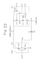
- a sense voltage curve of the S/A circuit in this embodiment is as shown in Fig. 3.
- a curve (3) represents a cell current characteristic curve after the data is written; and a curve (4) represents the cell current characteristic curve after the data is erased.
- Indicated at V W is a write verify source voltage
- V E is an erase verify source voltage. The data is discriminated to be "1" when a larger amount of current flows through the cell, and is discriminated to be "0" when a smaller amount of current flows through the cell, compared to the current indicated by the sense characteristic curves (1), (2).
- the Figure 2 embodiment provides another method for checking the verification which is carried out by applying the verify source voltage to the selected word line and this voltage is also applied only to a transistor used for comparing with a voltage level of the sense amplifier used in the reading operation, while the normal source voltage V CC is applied to any other components provided in the circuitry as in the normal reading operation.
- these two methods do not differ significantly from one another in terms of the discriminating level of the sensitivity of the sense amplifier. Accordingly, the verification can still be carried out at a specified operating power supply margin in a memory embodying the present invention.
- the verify voltage circuit 8 supplies the voltage only to the transistor 14, this embodiment is advantageous in terms of a supply ability of the verify voltage circuit. In other words, the size of a transistor contributing to supply the current, provided in the circuit, can be prevented from being increased by avoiding waste.
- Fig. 4 shows an exemplary construction of the verify voltage circuit 8.
- the circuit illustrated in Fig. 4 includes resistors 31 to 33 connected in series between a write/erase voltage line V PP and a power supply line V SS , an n-channel transistor 34 having a source thereof connected to a connection node between the resistors 31, 32 and responsive to a write verify signal WV, an n-channel transistor 35 having a source thereof connected to a connection node between the resistors 32, 33 and responsive to an erase verify signal EV, an n-channel transistor 36 whose source is connected to the respective drains of the transistors 34, 35 and whose gate is connected to its own drain, a p-channel transistor 37 whose source is connected to the respective drains of the transistors 34, 35 and whose gate is connected to its own drain, a current supply 38 connected between the voltage line V PP and the drain of the transistor 36, a current supply 39 connected between the drain of the transistor 37 and the power supply line V SS , an n-channel transistor 40 and a p-channel transistor 41 connected in series between the voltage line V
- the resistors 31 to 33 divide the write/erase voltage V PP (12V).
- resistance values of the respective resistors are set so that the potential at the connection node between the resistors 31, 32 is 6.5V (maximum voltage for the write verification) and the potential at the connection node between the resistors 32, 33 is 3.5V (minimum voltage for the erase verification).
- the transistors 36, 37, 40, 41 and the current supplies 38, 39 constitute a form of current mirror circuit, which functions so that an output voltage (verify voltage V VER ) becomes equal to the potential at the connection node between the transistors 36, 37.
- the normal supply voltage (V CC ) is an intermediate value between a first verify voltage which is the erase verify voltage and a second verify voltage which is the write verify voltage.
- the desirable range of the write verify source voltage V W and the erase verify source voltage V E can be determined with reference to the graphs as shown in Fig. 3.
- the transistor 34 is turned on.
- the potential at the node of the resistors 31, 32 i.e., the voltage of 6.5V
- the transistor 35 is turned on.
- the potential at the node of the resistors 32, 33 i.e., the voltage of 3.5V
- the potential at the node of the resistors 32, 33 i.e., the voltage of 3.5V
- the verify voltage V VER of 3.5V can be obtained by the current mirror action.
- the transistors 34, 35 are cut off. As a result, only the current mirror circuit operates and an intermediate level (5V) between 6.5V and 3.5V is output as the output voltage V VER . This output voltage is at the same level as the normal supply voltage V CC .
- an output signal of the S/A circuit is normally a weak signal in terms of the amplitude and drive ability, it is preferable to provide a buffer circuit for the purpose of stabilizing the output signal.
- the verify voltage V VER in which the voltage is changed from the bit line potential (about 1V) to the verify voltage V VER during the verification, it is preferable to supply the verify voltage V VER as a source voltage of the buffer circuit.
- Fig. 5 shows an exemplary construction of the S/A circuit including a buffer circuit.
- the illustrated circuit is obtainable by adding the buffer circuit to the construction of Fig. 2.
- This buffer circuit includes a p-channel transistor 16 and n-channel transistors 17, 18 which are connected in series between the verify source voltage line V VER and the power supply line V SS and are responsive to the drain potentials of the respective transistors 14, 15, and a p-channel transistor 19 which is connected between the voltage line V VER and a connection node between the transistors 17, 18 and is responsive to the drain potentials of the respective transistors 14, 15.
- the output of the S/A circuit (data output) is taken from the drains of the respective transistors 16, 17.
- the sense characteristic curves shown in Fig. 3 are ideally required to be devised.
- the inclination of the sense characteristic curve is preferably large in the neighborhood of the write verify source voltage V W so that a large power supply margin is taken for a change of a threshold voltage of the cell transistor.
- the inclination of the sense characteristic curve is preferably small in the neighborhood of the erase verify source voltage V E so as to make it easier to adjust the voltage V E finely and in order to improve the stability of the characteristic in terms of differences among cell transistors.
- Fig. 6 shows ideal sense characteristic curves
- Fig. 7 shows an exemplary construction of a preferable S/A circuit for realizing this characteristic.
- the illustrated circuit is obtainable by adding two transistors 20 and 21 to the construction of the S/A circuit including the buffer circuit shown in Fig. 5.
- the transistor 20 is a p-channel transistor, and is connected between the verify source voltage V VER and the source of the transistor 14. A gate of the transistor 20 is connected to a drain thereof. Accordingly, this transistor 20 functions as a voltage reducing element.
- the transistor 21 is an n-channel transistor of the depletion type, and is connected between the voltage V VER and the commonly-connected drains of the transistors 14,15. A gate of the transistor 21 is connected to a source thereof. Accordingly, this transistor 21 functions as a constant current supplying element.
- the portion of the overall memory circuit to which the verify source voltage should be applied may be confined just to the selected word line and the transistor used for comparing with a voltage level provided in the sense amplifier.
- the number of the portions to which the verify source voltage should be applied in the verify operation can be significantly reduced as compared with the conventional method in which the source voltage V CC applied to each of the components provided in the memory circuit is simply and uniformly converted to the verify source voltage. Accordingly, in the present invention, the number of the circuit elements to which the source voltage should be applied is remarkably small, thereby making it possible to reduce the performance required of the verify source voltage generating circuit used for supplying the verify source voltage. Accordingly, this generating circuit can be made significantly smaller than the comparable generating circuit required by the conventional method and thus the area to be occupied by the verify source voltage generating circuit can be significantly reduced whilst still maintaining suitable sensitivity in the verifying operation.
- a plurality of different power-supply voltages are used at different places, and many of them are supplied from external power supplies.
- a single external power supply should preferably be used to produce a plurality of different power-supply voltages within the flash-type memory embodying the present invention.
- an external power-supply voltage (normally, 5V) is dropped to a suitable low voltage within the device (namely, the power-supply voltage is simply dropped).
- the transistors are adapted to the reduced voltage so as to maintain characteristics thereof.
- Fig. 10 shows an example voltage dropping circuit used in the conventional semiconductor device
- Fig. 11 shows its operational characteristic waveform.
- Vcc indicates an external power-supply voltage (power line), Vss a reference power-supply voltage (power line) of the semiconductor device, and Vci an internally dropped voltage.
- the circuit illustrated in Fig. 10 comprises a constant-current source IS connected to the power line Vcc, n-channel transistors QT1 to QTn connected in series between the output terminal of the constant-current source IS and the power line Vss and each of which has a gate connected to the drain thereof, and an n-channel transistor Q30 connected between the power line Vcc and the internal-voltage (Vci) delivery node and which responds to a signal at the drain terminal of the transistor QT1.
- the internal voltage Vci is stabilized at the level of V2 when the external voltage Vcc is higher than the level of V1, thus advantageously, an ideal voltage drop is obtainable.
- the gate potential (reference voltage) of the transistor Q30 for conversion of the external voltage Vcc to the dropped voltage Vci is determined based on the voltage drop (threshold level) of each of the transistors QT1 to QTn, a problem will occur when the ambient temperature changes, the power-supply voltage varies or the like. Namely, the voltage drop of each of the transistors QT1 to QTn varies and the gate potential of the transistor Q30 also varies correspondingly, so that the operation of the transistor Q30 loses stability, thereby resulting in unstable delivery of the lowered voltage Vci.
- the constant-current source IS is used to generate a voltage drop in each of the transistors QT1 to QTn,some current is always consumed, which is a significant disadvantage.
- Fig. 12 shows an example address input circuit used in the conventional semiconductor device.
- the circuit shown in Fig. 12 comprises a p-channel transistor Q31 driven by a dropped voltage Vci produced in, for example, the voltage dropping circuit shown in Fig. 10.
- the p-channel transistor Q31 is connected at the source thereof to the potential Vss.
- a CMOS inverter (composed of a p-channel transistor Q32 and n-channel transistor Q33) is connected between the drain of the transistor Q31 and the power line Vss and responds to the address input signal; an n-channel transistor Q34 is connected parallel to the transistor Q33 and receives at its gate the potential Vss; and a CMOS inverter (composed of a p-channel transistor Q35 and n-channel transistor Q36) is connected between the power lines Vci and Vss and responds to the output from the inverter (Q32 and Q33).
- the circuit Since the input threshold level of the input circuit is lower because this circuit is driven by the internally dropped voltage Vci, the circuit is susceptible to noise compared to the case when driven by an ordinary power-supply voltage Vcc higher than the voltage Vci. For example, the transistor will possibly malfunction as a result of an internally developed noise.
- the noise component (coupling noise) caused by the capacitive coupling with the external signal line and will be larger.
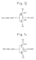
- Fig. 13 shows an example data output circuit used in the conventional semiconductor device.
- this circuit comprises a CMOS inverter (composed of a p-channel transistor Q37 and an n-channel transistor Q38) driven by the dropped voltage Vci produced in, for example, the voltage dropping circuit shown in Fig. 10.
- the inverter is connected between the dropped voltage line Vci and the power line Vss and responds to the data signal from the internal circuit.
- this circuit Since this circuit is driven by the internally dropped voltage Vci, when the data signal from the internal circuit changes in amplitude to the levels of the voltages Vci to Vss, the output signal also changes correspondingly with the amplitude at the levels of the voltages Vci to Vss. Thus, if a circuit connected to the output stage of this data output circuit is driven by an ordinary power-supply voltage (5V), matching with elements used in that circuit will be poor. A signal at a predetermined logical level may not be transmitted stably, as the case may be.
- Fig. 14 shows another example data output circuit in the conventional semiconductor device.
- This circuit comprises a CMOS inverter (composed of a p-channel transistor Q39 and an n-channel transistor Q40) driven by the external power-supply voltage Vcc .
- the inverter in this case is connected between the power lines vcc and Vss and which responds to the data signal from the internal circuit.
- an internal power-supply voltage generation circuit for use in a flash-type memory that can maintain a good matching with various elements including external elements even in the case that an external voltage and an internally dropped voltage are used together, and which contributes to the improvement of operational reliability by eliminating the influence of noise.
- the internal power-supply voltage generation circuit should also have a simple configuration, should not develop therein such through currents as in the conventional voltage dropping circuit, and should be very suitable for building an internal power-supply voltage generation circuit in which the CMOS configuration is adopted.
- the basic technical concept is to adjust the threshold of the main transistors composing the internal power-supply source voltage generation circuit while both the external power-supply voltage and reference voltage are kept at a stable fixed level to generate a dropped voltage at a predetermined level.
- the internal power-supply voltage generation circuit incorporates a circuit that drops an external power-supply voltage and the performance of which can be ensured with a wide range of power-supply voltages.
- the internal power-supply voltage generation circuit in the preferred embodiment of the present invention comprises, to solve the aforementioned problems, a means of dropping an external power-supply voltage to a predetermined internal voltage.
- This voltage dropping means is characterized in that a transistor is connected between the power-supply voltage line and the node at which the internal voltage is developed and that a reference voltage at a predetermined level is applied to the gate of the transistor so as to deliver the internally dropped voltage at the internal-voltage delivery node.
- the flash-type memory comprises a cell matrix circuit (1) having disposed therein reloadable nonvolatile memory cells (Mij) at the intersections of a plurality of word lines WL1 to WLm and a plurality of bit lines BLll to BLlk, ..., BLnl to BLnk, a row decoder circuit 3, a column decoder 5, sense amplifier circuits 71 to 7n connected to the bit lines BLll to BLlk, ..., BLnl to BLnk of the cell matrix circuit (1), and an internal power-source voltage generation circuit connected to at least an external power supply and in which an external power-supply voltage Vcc is used to produce different kinds of internal voltages.
- reloadable nonvolatile memory cells Mij
- the internal power-supply voltage generation circuit comprises a means of dropping an external power-supply voltage Vcc to a predetermined internal voltage Vci.
- This voltage dropping means has a transistor Q connected between the external power-supply voltage line and the node N at which the internal voltage is delivered.
- a reference voltage at a predetermined level is applied to the gate of the transistor Q to deliver the internally dropped voltage at the internal-voltage delivery node.
- the transistor Q should preferably be a depletion-type n-channel transistor.
- a smoothing capacitor C may be provided in the internal-voltage delivery node in the internal power-source voltage generation circuit, whereby the internal source voltage resulting from noise or the like can be prevented from fluctuating.
- the voltage dropping level can be adjusted by changing the threshold of the aforementioned transistor Q.
- the fixed reference voltage applied to the gate of the transistor Q should preferably be a single voltage supplied from the reference power line Vss of the semiconductor device.
- the reference voltage at the predetermined level applied to the gate of the transistor Q may be supplied to the reference power line of the semiconductor device, whereby only the dropped voltage is delivered at the internal-voltage delivery node.
- nonvolatile memory elements may be used and the reference voltage at the predetermined level applied to the gate of the transistor Q should be set to either the level of the external power-source voltage or that of the reference power-source voltage of the semiconductor device, whereby a dropped voltage or an ordinary power-source voltage is selectively delivered at the internal-voltage delivery node.
- a smoothing capacitor may be provided in the internal-voltage delivery node to further stabilize the level of the internally dropped voltage delivered at the node.
- Embodiments of the preferred internal power-supply voltage generation circuit will be described with reference to Figs. 15 to 20.
- Fig. 15 shows an example configuration of the voltage dropping circuit in the internal power-supply voltage generation circuit.
- a depression-type n-channel transistor Q is used to convert an external power-supply voltage Vcc to an internal voltage dropped for the internal circuit.
- a smoothing capacitor C is connected between the internal-voltage delivery node N and the lower-potential power line Vss.
- the transistor Q provided for converting a stable external power-source voltage Vcc to a dropped internal voltage Vci is connected at the gate thereof to the reference voltage line Vss, the potential of which is stable and does not fluctuate. Since there is no problem that a current is always supplied as in the circuit configuration shown in Fig. 10, a stable internally-dropped voltage Vci can be obtained.
- the threshold of the transistor used in the internal power-source voltage generation circuit embodying the present invention can be adjusted by changing, for example, the silicon oxide film thickness.
- Fig. 16 shows an example of such a circuit.
- the circuit shown in Fig. 16 comprises a nonvolatile memory cell QM such as EPROM to determine whether the internally dropped voltage Vci or the external voltage Vcc is to be delivered.
- the nonvolatile memory cell QM is connected between the reference power line Vss and an internal-voltage delivery node P and has its control gate connected to the supply line of the external voltage Vcc.
- the nonvolatile memory cell QM supplies or does not supply a current according to its contents. Therefore, the potential at the internal-voltage delivery node P takes the L level when the memory cell QM supplies a current, and takes the H level when the memory cell does not supply a current.
- a p-channel transistor Q1 is connected between the power line Vcc having a high potential and the internal-voltage delivery node P. Also a CMOS inverter (composed of a p-channel transistor Q2 and an n-channel transistor Q3) is connected between the power line Vcc and the low voltage line Vss, and these transistors are connected at the respective gates thereof to the internal-voltage delivery node P and at the respective drains thereof to the gate of the p-channel transistor Q1.
- CMOS inverter Composed of a p-channel transistor Q4 and an n-channel transistor Q5, the gates of which are connected to the output terminals of the inverter (Q2 and Q3) and the drains of which are connected to the gate of the transistor Q (Fig. 15).
- the gate of the transistor Q provided for conversion of the power-source voltage Vcc to an internal source voltage Vci is so arranged as to receive a voltage determined in dependence upon the contents of the nonvolatile memory cell QM (namely, the H or L level developed at the internal-source voltage delivery node P) instead of receiving the fixed reference potential Vss as in the embodiment shown in Fig. 15.
- the internal-source voltage delivery P takes the L level.
- the transistor Q is supplied at the gate thereof with an L-level signal through the two-stage inverter, and this transistor is cut off.
- a dropped internal source voltage vci is delivered at the internal-source voltage delivery node N.
- the internal-source voltage delivery node P takes the H level, so that the transistor Q is turned on and thus the external power-source voltage Vcc is delivered at the internal-source voltage delivery node N.
- Fig. 17 shows an example configuration of the input-stage circuit in a semiconductor device in which the aforementioned voltage dropping circuit is adopted.
- the input-stage circuit shown in Figure comprises circuitry driven by an external power-source voltage Vcc and circuitry driven by the dropped internal source voltage Vci, and it is so configured as to transmit an input signal Si (for example, an address signal in case of a semiconductor memory) to an internal circuit of which at least a part is driven by the internally dropped voltage Vci.
- Si for example, an address signal in case of a semiconductor memory
- the circuitry driven by the external power-source voltage Vcc comprises: a p-channel transistor Q11, connected at the source thereof to the power line Vcc, that responds to the potential Vss; a CMOS inverter (composed of a p-channel transistor Q12 and an n-channel transistor Q13), connected between the drain of the transistor Q11 and the power line Vss,that responds to the input signal Si; an n-channel transistor Q14, connected parallel to the transistor Q13,that responds to the potential Vss; and a CMOS inverter (composed of a p-channel transistor Q15 and an n-channel transistor Q16), connected between the power lines Vcc and Vss,that responds to the output from the inverter (Q12 and Q13).
- the transistors Q15 and Q16 function to stabilize the level of signals having amplitudes Vcc to Vss delivered from the circuit provided upstream thereof and transmit them to the circuit provided downstream thereof.
- the circuitry driven by the internally dropped voltage Vci comprises: a CMOS inverter (composed of a p-channel transistor Q17 and an n-channel transistor Q18),connected between the internally-dropped voltage line Vci and the power line Vss,that responds to the output from the inverter (Q15 and Q16); and a CMOS inverter (composed of a p-channel transistor Q19 and an n-channel transistor Q20), connected between the power lines Vci and Vss, that responds to the output from the inverter (Q17 and Q18).
- the input threshold level can be set high compared to that in the conventional circuit configuration (shown in Fig. 12 ). Namely the circuitry is not susceptible to noise in an external input signal (that is, improvement in the noise margin of the circuit) and the possibility of a transistor malfunction can be eliminated.
- the gate withstand voltage of each transistor used in that circuitry is preferably selected so as to be relatively high.
- the drain or gate withstand voltage of each transistor used in the circuitry driven by the external power-supply voltage Vc should preferably be set high.
- Fig. 18 shows an example configuration of the output-stage circuit in a semiconductor device in which the aforementioned voltage dropping circuit is adopted.
- the output-stage circuit shown in the Figure comprises circuitry driven by the dropped internal voltage Vci and circuitry driven by the external power-supply voltage Vcc, and it is so configured as to deliver outside the circuit, as data output So, a data signal from an internal circuit (not shown) at least a part of which internal circuit is driven by the internally dropped voltage Vci.
- the circuitry driven by the internally dropped voltage Vci comprises a CMOS inverter (composed of a p-channel transistor Q21 and an n-channel transistor Q22), connected between the internally dropped voltage line Vci and the power line Vss, that responds to the above-mentioned data signal, and an n-channel transistor Q23 connected at the source thereof to the output terminal of the CMOS inverter and at the gate thereof to the internally dropped voltage line Vci.
- CMOS inverter composed of a p-channel transistor Q21 and an n-channel transistor Q22
- the circuitry driven by the external power-supply voltage Vcc comprises: a p-channel transistor Q24 connected between the drain of the transistor Q23 and the power line Vcc; a CMOS inverter (composed of a p-channel transistor Q25 and an n-channel transistor Q26), connected between the power lines Vcc and Vss, that responds to the signal at the drain terminal of the transistor Q24 and that provides an output signal applied to the gate of the p-channel transistor Q24; and a CMOS inverter (composed of a p-channel transistor Q27 and an n-channel transistor Q28), also connected between the power lines Vcc and Vss, that is operative in response to the output signal from the inverter (Q25 and Q26) to produce a data output So.
- the data signal from an internal circuit is converted to the level of the external power-supply voltage Vcc by means of the level converting means (transistors Q23 and Q24) and delivered outside the circuit as a data output So having amplitudes of the voltage Vcc to Vss. Therefore, in the case that the external circuit connected to this output-stage circuit is driven by an ordinary power-supply voltage (5V), matching with the elements used in this external circuit can be maintained. Namely, a stable predetermined logical-level signal can be transmitted.
- the above-mentioned level converting means works in such a manner that the transistors Q25 and Q26 are supplied at the gates thereof with signals having amplitudes of the voltages Vcc to Vss. Thus both transistors are not turned on together, so that a through current will not flow from the power line Vcc to the power line vss through these transistors.
- the drain or gate withstand voltage of each transistor used in the circuitry driven by the external power-source voltage Vcc should preferably be relatively high.
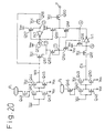
- Fig. 19 shows the configuration of a semiconductor device in which the circuit shown in Fig.16 is adopted.
- the reference numeral 410 denotes a voltage dropping circuit comprising a data write/erase circuit (see Fig.20 ) of the nonvolatile memory cell and the voltage dropping circuit shown in Fig.16.
- the voltage dropping circuit 410 works with the normal source voltage Vcc and a high voltage Vpp for data write/erase with respect to the nonvolatile memory cell.
- the reference numeral 420 denotes circuitry comprising an address buffer, a decoder, a memory cell and a sense amplifier, and this circuitry works with an internally dropped voltage developed at the output terminal (node N) of the voltage dropping circuit 410.
- reference numeral 430 denotes a first-stage address buffer which, upon receiving the power-source voltage Vcc, buffers and address input, and 440 an output buffer which, also upon receiving the power-source voltage Vcc, delivers a data output.
- Fig. 20 shows an example configuration of the data write/erase circuit of the nonvolatile memory cell in the voltage dropping circuit 410.
- the circuit for controlling the write operation to the nonvolatile memory cell QM comprises a p-channel transistor Q41 connected at the source thereof to a pad P1 and at the gate to the drain thereof, a CMOS inverter (composed of a p-channel transistor Q42 and an n-channel transistor Q43) connected between the drain of the transistor Q41 and the power line Vss that responds to the power-supply voltage Vcc, and a CMOS inverter (composed of a p-channel transistor Q44 and an n-channel transistor Q45) connected between the power lines Vcc and Vss that is operative in response to the output from the inverter (Q42 and Q43) so as to generate a write signal WX.
- the circuit for controlling the erase operation of the nonvolatile memory cell comprises a p-channel transistor Q46 connected at the source thereof to a pad P2 and at the gate to the drain thereof, a CMOS inverter (composed of a p-channel transistor Q47 and an n-channel transistor Q48) connected to the drain of the transistor Q46 and the power line Vss that responds to the power-supply voltage Vcc, and a CMOS inverter (composed of a p-channel transistor Q49 and an n-channel transistor Q50) connected between the power lines Vcc and Vss that is operative in response to the output from the inverter (Q47 and Q48) so as to produce an erase signal EX.
- the data write/erase circuitry of the nonvolatile memory cell QM comprises an n-channel transistor Q51 connected at the drain thereof to the power line Vcc that responds to the write signal WX, an n-channel transistor Q52 connected at the drain thereof to the high voltage power line Vpp that responds to the potential at a node 3, an n-channel transistor Q53 connected at the drain thereof to the source of each of the transistors Q51 and Q52 and at the gate to the source thereof node 1), an n-channel transistor Q54 connected between the node 1 and the power line Vss that responds to the potential at a node 4, an n-channel transistor Q55 connected between the output terminal of erase signal EX and node 5 that responds to the power-supply voltage Vcc, a p-channel transistor Q56 connected between the high voltage power line Vpp and the node 5 that responds to the potential at the node 4, an inverter IV1 connected in the forward direction between the nodes 5 and 4, a p-channel transistor Q57 connected between the
- the data write/erase circuit shown in Fig. 20 functions as explained below:
- both the write signal WX and the erase signal EX take the L level.
- the Figures 15 to 20 embodiments of of the present invention can permit a reduction in power consumption and stably supply an internally dropped voltage in a semiconductor device in which a circuit to drop an external power-source voltage is incorporated.
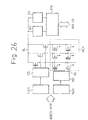
- Fig. 26 is a block diagram of an EPROM used in the conventional flash-type memory.
- the EPROM comprises a memory cell array MCA disposed in a matrix, a column address buffer CAB, a column decoder CD, a row address buffer RAB, a row decoder RD, a write circuit WC, a sense amplifier SA and an input/output data buffer IOB.
- the row decoder RD selects the word line WL
- the column decoder CD selects the bit line BL, thus selecting a single memory cell with respect to which write or read data is put through the input/output buffer IOB.
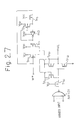
- Fig. 27 is a circuit diagram of the decoder.
- the write control signal W# (# means that the signal in consideration is a negative-logic signal) takes the L level, and the power-supply voltage Vpp is applied to the word line WL.
- the write control signal W# takes the H level and the power-supply voltage is applied to the word line WL. Further, for verification the write control signal W# remains at the H level and verification is completed with the power-supply voltage Vcc raised above the ordinary read voltage.
- a write operation to the EPROM is effected with a specially designed writer, and when a conventional writer is used for such a write, the power source-voltage Vcc will be 5 or 6V. Therefore, it is necessary to use the voltage dropping circuit shown in Figs. 10 and 11 in order to inhibit the power-source voltage Vcc (Vci) to the internal circuit from rising above a predetermined value. In this case, verification of the type referred to above is impossible since the power-source voltage Vci to the internal circuit is inhibited by the voltage dropping circuit from rising above the predetermined value.
- the conventional flash-type memory it is necessary to change the read voltage to a lower voltage in order to minimize power consumption as described in the foregoing. If the conventional write operation is used for a data write to the memory, the power-source voltage to the internal circuit should be prohibited by the voltage dropping circuit from rising above a predetermined value. However, verification in the conventional manner cannot be done in this case.
- preferred embodiments of the present invention seek to solve the above problems by providing a flash-type memory in which the read voltage is changed to a lower voltage to minimize power consumption and that can effect the verification and provide a stable device operation even when operated with a voltage produced by internally dropping the power-source voltage.
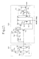
- a first embodiment shown in Fig. 21 relates to an internal power-source voltage generation circuit adapted so as to receive an external power-source voltage vcc for a data read and an external power-source voltage vpp for a data write, and which comprises a means of operating the read circuit in the flash-type memory by dropping the read external power-source voltage Vcc to a predetermined value and a means of producing a word-line potential for post-write verification by dropping the write external power-source voltage Vpp.
- a second embodiment shown in Fig. 22 provides an internal power-source voltage generation circuit adapted to receive a read external power-source voltage Vcc and a write external power-source voltage Vpp that comprises a means of operating the read circuit inside the flash-type memory by dropping the read external power-source voltage Vcc to a predetermined value and a means of producing a word-line potential for post-write verification by internally generating a voltage higher than a voltage obtained by dropping the read external power-source voltage Vcc.
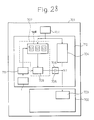
- Fig. 23 shows a third embodiment of the preferred internal power-supply voltage generation circuit, which is adapted to receive a read external power-source voltage Vcc and a write external power-source voltage Vpp, and comprises a means of operating the read circuit in the flash-type memory by dropping the read external power-source voltage Vcc to a predetermined value and a means of inhibiting the read external power-source voltage Vcc from being dropped at the time of post-write verification.
- the internal power-source voltage generation circuit is adapted to receive a read external power-source voltage Vcc and a write external power-source voltage Vpp, and comprises a means of operating the read circuit inside the flash-type memory by dropping the read external power-source voltage Vcc to a predetermined value and a means of normally making the sense current of a sense amplifier smaller than the read sense current.
- the first embodiment has a power-source voltage selector comprising, as shown in Fig. 21, a Vpp detection circuit 501 that detects whether or not the write external power-source voltage Vpp is supplied, and a selection circuit 503 that supplies a word-line potential.
- This power-source voltage selector is so arranged that when the write external power-source voltage Vpp is supplied, the voltage Vci (power to the internal circuit) provided by dropping the read external power-source voltage Vcc to a predetermined value is disconnected and for verification, the write external power-source voltage Vpp is dropped to provide a word-line potential for post-write verification.
- the power-source voltage selector comprises, as shown in Fig. 22, a Vpp detection circuit 501 that determines whether or not the write external power-source voltage Vpp is supplied, and a selection circuit 503' that supplies a word-line potential. It is so arranged that when the write external power-source voltage Vpp is supplied, the voltage Vci (power to the internal circuit) derived from dropping the read external power-source voltage Vcc to a predetermined value is supplied as a word-line potential, whereas for the post-write verification, a voltage obtained by raising the voltage produced by dropping the read external power-source voltage Vcc is supplied as the word-line potential. Thus, good verification can be implemented.
- the power-source voltage selector in the third embodiment comprises, as shown in Fig. 23, a voltage dropping circuit provided for the read circuit in the flash-type memory that drops the read external power-source voltage Vcc to a predetermined voltage, and a means of inhibiting the voltage supply produced by dropping the read external power-source voltage Vcc under control of the Vpp detection circuit 501, which detects whether or not the write external power-source voltage Vpp is supplied, whereby the read external power-source voltage Vcc is used as it is for the word-line potential for post-write verification.
- a good verification can be effected.
- the sense current of the sense amplifier is made smaller than that for the ordinary read for verification, as shown in Fig. 24, so that a stable operation on the power-source voltage Vci to the internal circuit can be ensured and a good verification can be effected.
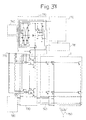
- Fig. 21 is a circuit diagram of the power-source voltage selector in the flash-type memory according to the first embodiment.
- the general configuration of the flash-type memory according to this embodiment is the same as that shown in the block diagram in Fig. 26 and additionally includes the power-supply voltage selector shown in Fig.21 and the voltage dropping circuit shown in Fig. 10.
- the power-supply voltage selector in the flash-type memory comprises a Vpp detection circuit 501 that determines whether or not the write external power-source voltage Vpp is supplied, and a selection circuit 503 that supplies the column decoder and the row decoder with the power-source voltage (word-line potential) after changing.
- the Vpp detection circuit 501 comprises p-channel MOS transistors Tpl, Tp2 and Tp3 and n-channel MOS transistors Tnl and Tn2, thereby changing the Vpp detection signal R to L level when the write external power-source voltage Vpp is supplied.
- the selection circuit 503 supplies, as a power-source voltage (word-line potential) to the column decoder and the row decoder, a voltage produced by dropping the write external power-source voltage Vpp. Namely, when the write external power-source voltage Vpp is supplied, the Vpp detection signal R takes the L level and the power-source voltage Vci (to the internal circuit) produced by dropping the reads external power-source voltage Vcc by the voltage dropping circuit shown in Fig. 10 is disconnected by the n-channel MOS transistor Tn7.
- the n-channel MOS transistor Tn6 is turned on and the write external power-supply voltage Vpp is supplied as a power-source voltage to the column decoder and the row decoder, respectively, or when the Vpp detection signal R is at the L level, the p-channel MOS transistor Tp5 is turned on so that if the write control signal W# is at the H level (for verification), a voltage Vpp' derived from voltage division of the write external power-source voltage Vpp by resistors R1 and R2 is supplied to the column decoder and the row decoder, respectively.
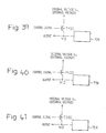
- Fig. 22(A) is a circuit diagram of the power-source voltage selector in the flash-type memory according to the second embodiment.
- the general configuration of the flash-type memory according to this embodiment is the same as that shown in the block diagram in Fig. 26 and additionally includes the power-source voltage selector shown in Fig. 22(A) and the voltage dropping circuit shown in Fig.10.
- the power-source voltage selector comprises a Vpp detection circuit 501 that is identical to that shown in Fig. 21 and a selection circuit 503'.
- the selection circuit 503' supplies a voltage produced by an internal verification source voltage generation circuit 513 as a power-source voltage to the column and row decoders.
- the verification source voltage generation circuit 513 comprises a booster circuit composed of n-channel MOS transistors Tnll, Tn12 and Tn13 and capacitors C1 and C2 as shown in Fig. 22(B). Namely, the power-source voltage Vci to the internal circuit, produced by the voltage dropping circuit shown in Fig. 10, is raised and used as a power-source voltage to the column and row decoders. Note that the capacitors C1 and C2 are supplied with voltages ⁇ 1 and ⁇ 2 having the waveforms shown in Fig. 22 (C).
- the selection circuit 503' is so arranged that when the write external power-source voltage Vpp is supplied (the Vpp detection signal R is at the L level), the power-source voltage Vci is disconnected by the n-channel MOS transistor Tn7. If the write control signal W# is at the L level (for write), the write external power-source voltage Vpp is supplied as the power-source voltage to the column and row columns, respectively. If the write control signal W# is at the H level (for verification), the internal voltage boosted by the verification source voltage generation circuit 513 is supplied as the power-source voltage to the column and the row decoders, respectively.
- Fig. 23 is a circuit diagram of the power-source voltage selector in the flash-type memory according to the third embodiment. Note that the general configuration of this flash-type memory is identical to that shown in the block diagram in Fig.26 and additionally includes the power-source voltage selector shown in Fig. 23.
- the power-source voltage selector in this embodiment includes a p-channel MOS transistor Tp21 added to the voltage dropping circuit shown in Fig. 10 that is controlled with the Vpp detection signal R from the Vpp detection circuit 501; the transistor Tp21 serving to inhibit the word-line drive component from being dropped for the verification.
- the write external power-source voltage Vpp is supplied and the Vpp detection signal R takes the L level and the p-channel MOS transistor Tp21 is turned on so that the read external power-source voltage Vcc is supplied as it is as the power-source voltage (word-line potential) to the column and row decoders, respectively.
- the Vpp detection signal R takes the L level and the p-channel MOS transistor Tp21 is turned on so that the read external power-source voltage Vcc is supplied as it is as the power-source voltage (word-line potential) to the column and row decoders, respectively.
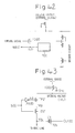
- Fig. 24 is a circuit diagram of the sense amplifier in the flash-type memory according to the fourth embodiment. It should be noted that the general configuration of the flash-type memory according to this fourth embodiment is identical to that shown in Fig. 26 and additionally includes the Vpp detection circuit shown in Fig. 21 and the voltage dropping circuit shown in Fig. 10.
- the sense current of the sense amplifier SA is made smaller than that for the ordinary read, thereby attaining a good verification.
- the sense amplifier SA has two p-channel transistors Tp41 and Tp42 which form together a load circuit.
- the Vpp detection signal R# from the Vpp detection circuit is supplied to the gate of one (Tp42) of these transistors to supply a sense current to the bit line BL of the memory cell.
- the Vpp detection signal R# takes the L level for data read, the p-channel MOS transistor Tp42 is turned on and the sense current has a larger value as shown in Fig. 5.
- the characteristic of the memory cell changes as indicated with the curve A for the verification, but by changing it to the sense current value for the data read, it is possible to provide an operational voltage margin for Vw-Vci.
- the sense current of the sense amplifier SA is made smaller than that for the ordinary read, whereby a stable operation with the power-supply voltage Vci to the internal circuit can be ensured.
- the first embodiment ( Figure 21) is so configured that when the write external power-source voltage-is supplied, the voltage produced by dropping the read external power-source voltage to a predetermined value for the verification, the voltage obtained by dropping the write external power-source voltage is supplied as the word-line potential for the post-write verification.
- an internal power-source voltage generation circuit can be provided in which verification can be effected even when the memory is operated with a voltage produced by internally dropping the power-source voltage and a stable device operation can be ensured.
- the second embodiment ( Figure 22) is so arranged that, when the write external power-source voltage is supplied, the voltage produced by dropping the read external power-source voltage V to a predetermined value is disconnected and a voltage produced by boosting a voltage derived from dropping of the read external power-source voltage is supplied as the word-line potential for the post-write verification.
- the second embodiment provides an internal power-source voltage generation circuit for a flash-type memory, which can provide a good verification.
- the third embodiment provides an internal power-source voltage generation circuit for a flash-type memory, comprising a voltage dropping circuit provided for the read circuit in the flash-type memory that drops the read external power-source voltage Vcc to a predetermined value, and a means of inhibiting the supply of a voltage derived by dropping the read external power-source voltage under the control of the Vpp detection circuit, which detects whether or not the write external power-source voltage is supplied, whereby the read external power-source voltage Vcc is supplied as it is as the word-line potential for the post-write verification so that a good verification can be ensured.
- a read external power-source voltage Vcc and a write external power-source voltage Vpp are used and the read circuit in the flash-type memory is operated with a voltage produced by raising or boosting the read external power-source voltage Vcc to a predetermined voltage, and for the verification, the sense current of the sense amplifier SA is made smaller than that for the ordinary read, whereby a stable operation with the power-source voltage Vci to the internal circuit can be ensured and a good verification can be done.
- the data readout operation alone, for example, includes the readout modes of at least three different kinds of systems, that is, the normal readout mode, the erase verify mode at the time of erase and the write verify mode after writing.
- a power supply voltage generation circuit 790 for the first readout mode a power supply voltage generation circuit 791 for the second readout model
- a power supply voltage generation circuit 792 for the n th readout mode by the use of a mode selection circuit 793, and to supply the selected voltages to a decoder through a suitable booster circuit.
- a variance necessarily occurs between these power supply voltages, and the correlationship described above is likely to collapse.
- Such a problem results from the fact that a predetermined power supply voltage is formed from different power supply voltages by individual booster circuits.
- the or each power supply voltage that cannot be supplied directly from an external power supply must be generated inside the semiconductor memory device to match each mode.
- a power supply circuit for use in a semiconductor memory device such as a flash memory having a power supply voltage generation function, which can solve the problems with the prior art described above, and which can easily generate a plurality of kinds of different power supply voltages.
- the power supply circuit for a non-volatile semiconductor memory device embodying the present invention preferably employs the following technical construction.
- the semiconductor memory device has a plurality of kinds of readout modes and requires a different power supply voltage for each of these modes, and comprises power source voltage input unit, reference voltage generation means, boost means including a capacitance device, and charge means for charging the capacitance device, the charge means of the capacitance device including charge quantity change means for changing the charge quantity of the capacitance device into a plurality of kinds in response to mutually different voltages.
- such a power supply voltage circuit uses a single external reference power supply source and one booster circuit, and generates a plurality of kinds of power supply voltages. More definitely, the reference source voltage is used as the first power source voltage by the use of one capacitance device and at the same time, a voltage necessary for generating mutually different voltages necessary for the readout modes is charged in advance in the capacitance device constituting the boost means, and at a predetermined timing control signals each having a voltage amplitude necessary to generate respective voltage the level of which is different from each other from the capacitance device, are applied to the capacitance device so that a plurality of kinds of mutually different, necessary power supply voltages can be generated by adding and combining the output charged voltage with the reference voltage.
- the correlationship between the power supply voltages of the readout modes is determined only by the amplitude of the signal input to the capacitance device, or only by the voltage charged in advance in the capacitance device, or by both of them.
- the power supply voltage can be controlled by controlling only the input signal or the charge voltage, so that setting of the power supply voltages becomes easier and the correlationship between the power supply voltages of the readout modes can be set more correctly.
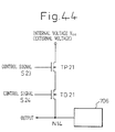
- Fig. 28 is a block diagram showing an example of the construction of the power supply voltage generation circuit 710 used in the semiconductor memory device according to this definite example.
- Fig. 28 illustrates a semiconductor memory device 701 which includes a logical circuit unit 702 having a plurality of kinds of readout modes, and which requires different power supply voltages for these readout modes.
- the semiconductor memory device 701 includes a power supply voltage input unit 703 and a power supply voltage generation circuit 710, which, in turn, includes reference voltage generation means 704, boost means 706 including a capacitance device 705, and charge means 707 for charging the capacitance device 705, the charge means 707 being equipped with charge quantity change means 707 for changing a charge quantity of the capacitance device 705 into a plurality of kinds in response to mutually different voltages required by the readout modes, respectively.
- the power supply voltage generation circuit 710 in the semiconductor memory device 701 generates a plurality of kinds of power supply voltages required by the logical circuit unit 702 by boosting the reference voltage by the capacitance device 705 and at the same time, changes the amplitude of a clock pulse signal input to the capacitance device 705 for generating the power supply voltage required by each readout mode in response to each of a plurality of kinds of power supply voltages required by the logical circuit unit 702, or changes the charge voltage to be charged in the capacitance device 705.
- the clock pulse signal having a different amplitude or the charge voltage having a different voltage is charged in the capacitance device 705 in accordance with a predetermined clock signal, and is added to, or subtracted from, the reference voltage so as to obtain a predetermined power supply voltage, which is output to the power supply voltage input unit 703 of the logical circuit unit 702 as the predetermined power supply voltage.
- the reference voltage generation means 704 in this definite example functions also as charge means for charging the capacitance device 705 constituting the boost means 706.
- its construction is not limited in particular, it may be constituted by connecting a P-channel enhancement type field effect transistor TP5 and an N-channel depletion type field effect transistor TD2 in series, connecting the gate of the P-channel enhancement type field effect transistor to the gate of the N-channel type depletion type field effect transistor TD2 through an inverter INV2, and connecting their common terminal to a suitable control terminal S1, as shown in Fig. 29.
- the free end portion of the P-channel type enhancement type field effect transistor TP5 in the reference voltage generation means 704 may be connected to a predetermined external power supply, or may be connected to an internal power supply voltage Vcc.
- the free end portion of the N-channel type depletion field effect transistor TD2 is connected to one of the ends of the capacitance device 705 disposed in the boost means 706.
- the power supply voltage generation circuit 710 in the semiconductor memory device 701 includes a suitable charge circuit 709 and charge quantity selection means 708 for changing the charge voltage to be charged in the capacitance device 705 constituting the boost means 706 into a plurality of kinds in accordance with the mutually different voltages required by the readout modes, respectively.
- the charge quantity selection means 708 is provided in advance with a plurality of kinds of voltage generation circuits capable of outputting a plurality of predetermined voltage levels, selects these voltage generation circuits by suitable selection means, supplies the selected voltage to the capacitance device 705, and boosts the voltage charged to the capacitance device 705 from the reference voltage generation means 704.
- the boost voltage is input to the power supply voltage input unit 703 of the logical circuit unit from a node portion N1 shown in Fig. 28.
- a predetermined clock pulse can be used as the charge quantity selection means.
- the charge quantity selection means 708 in this definite example may even be controlled by the signal from the clock circuit 711.
- the charge quantity change means 707 includes a suitable charge circuit 709 and at the same time, may be equipped with amplitude change means 712 for changing the amplitude of the clock pulse into the capacitance device 705 into a plurality of kinds in response to the mutually different voltages required by the readout modes, respectively.
- the amplitude change means 712 generates a predetermined pulse width control signal for the clock circuit 711 and changes the amplitude of this clock pulse into a plurality of kinds, so that the charge voltage charged in the capacitance device 705 disposed in the boost means 706 is changed.
- all of a plurality of kinds of readout modes in the semiconductor memory device according to this definite example may be connected to the power supply voltage circuit such as the one described above, or at least a part of the readout modes may be connected to such a power supply voltage circuit.
- the mutually different voltages required for a plurality of kinds of readout modes in this definite example are preferably generated from the same internal power supply voltage.
- Fig. 29 is a block diagram useful for explaining a definite example of the power supply voltage generation circuit 710 of the semiconductor memory device 701 of this definite example.
- the reference voltage generation means 704 in this definite example is constituted by connecting the P-channel enhancement field effect transistor TP5 in series with the N-channel depletion field effect transistor TD2, connecting the gate of the P-channel enhancement field effect transistor to the gate of the N-channel depletion field effect transistor TD2 through the inverter INV2, and further connecting their common terminal to a suitable first control terminal S1.
- the free end portion of the P-channel enhancement field effect transistor TP5 in the reference voltage generation means 704 may be connected to a predetermined external power supply or to the internal power supply voltage Vcc.
- the free end portion of the N-channel depletion field effect transistor TD2 is connected to one of the end portions of the capacitance device 705 disposed in the boost means 706 and to the power supply voltage input unit 703 in the logical circuit unit 702 of the semiconductor memory device.
- the charge quantity change means 707 in the power supply voltage generation circuit 710 includes a first transistor train 712 formed by connecting in series an N-channel depletion field effect transistor TD1, P-channel enhancement field effect transistors TP3 and TP4, and N-channel enhancement field effect transistor TN4 and TN5 in the order named, between the internal power supply voltage Vcc and the ground potential GND.
- the charge quantity change means 7 in the power supply voltage generation circuit 710 includes a second transistor train 713 formed by connecting in series P-channel enhancement field effect transistors TP1 and TP2, N-channel enhancement field effect transistors TN1 and TN2, and an N-channel enhancement field effect transistor TN3 between the internal power supply voltage Vcc and the ground potential GND in the order named.
- a clock terminal portion CLK1 which is disposed separately is connected to the gate of each of the P-channel enhancement field effect transistor TP4 and the N-channel enhancement field effect transistor TN4 and also to the gate of each of the P-channel enhancement field effect transistor TP2 and the N-channel enhancement field effect transistor TN2.
- a second control terminal S2 is connected to the gate of each of the N-channel enhancement field effect transistor TN3 and the P-channel enhancement field effect transistor TP3, and at the same time, to the gate of each of the N-channel enhancement field effect transistor TN5 and the P-channel enhancement field effect transistor PT1 through the inverter INV1.
- a third control terminal S3 is connected to the gate of the N-channel depletion field effect transistor TD1, and the internal power supply voltage Vcc is connected to the gate of the N-channel enhancement field effect transistor TN1.
- the output terminals N2-1 and N2-2 of the first and second transistor trains 712 and 713 are commonly connected to one of the end portions of the capacitance device 705.
- the charge voltage charged in the capacitance device 705 can be set to a predetermined voltage level by appropriately switching the control voltage applied to the control terminals S1, S2 and S3 and simultaneously applying the clock in a suitable cycle. Therefore, this voltage is added to the voltage which is in advance generated in the reference voltage generation means 704 and charged in the capacitance device 705, and the reference voltage is output as the boosted voltage from the output node portion N3.
- the control signal S1 is set to the "H” level so as to drive the reference voltage generation circuit 704. Accordingly, the voltage of the power supply voltage output unit N3 is charged to the power supply voltage Vcc (this will be referred to as the "first power supply voltage").
- the first control signal S1 is set to the "L” level at the point tl at which the power supply voltage output unit N3 is sufficiently charged, and the clock CLK1 is set to the "L” level at the point t2 which is somewhat retarded from the point tl at which the control signal S1 changes from the "H" level to the "L” level.
- the second inverter 712 constituted by the first transistor train 712 becomes effective, and since the third control signal S3 is at the "H” level, the potential at the connection node N1 between the N-channel depletion field effect transistor TD1 and the P-channel enhancement field effect transistor TP3 in the second inverter 712 becomes Vcc, so that the potential of the output node N2-1 changes from 0 V to Vcc.
- the potential at the power supply voltage output unit N3 is raised from Vcc to 2Vcc, and here, the second power supply voltage is generated.
- the control signal S1 is set to the "H” level and the voltage of the power supply voltage output unit N3 is charged to the internal power supply voltage Vcc.
- the first control signal S1 is kept at the "L” level and at the time t2 slightly delayed from the time t1, at which the signal level of the first control signal S1 is changed from “H” level to “L” level, the clock CLK1 is set to the "L” level.
- the potential of the power supply voltage output unit N3 is boosted from Vcc to Vcc + Vtd, and here, the third power supply voltage is generated (refer to Fig.30 (D)).
- the second control signal S2 is set to the "H” level.
- the control signal S1 is set to the "H” level, and the voltage of the power supply voltage output unit N3 is charged to the internal power supply voltage Vcc.
- the first control signal S1 is kept at “L” level and at the time t2 slightly delayed from the time tl, at which signal level of the first control signal S1 is changed from “H” level to “L” level, the clock CLK1 is set to the "L” level.
- the P-channel enhancement field effect transistor TP2 and the N-channel enhancement field effect transistors TN1 and TN2 are turned ON, so that the third inverter 713 consisting of the second transistor train 713 becomes effective, and the potential of the output node N2-2 as the connection node between the N-channel enhancement field effect transistors TN1 and TN2 in the third inverter 713 changes from 0 V to Vcc - Vth which is the difference obtained by subtracting the threshold voltage Vth of the N-channel enhancement field effect transistor TNI from Vcc.
- the potential of the power supply voltage output unit N3 is boosted from Vcc to 2Vcc + Vtn, and here, the fourth power supply voltage is generated (refer to Fig. 30(E)).
- control signals S1 to S3 in this definite example constitute the charge quantity selection means 708 for changing the charge voltage to be charged in the capacitance device 705 in this definite example into a plurality of kinds of voltages.
- this definite example makes it possible to extract four different kinds of power supply voltages from the same internal power supply voltage Vcc, and this operation can be executed by adjusting the application timings of the control signals S1 to S3 and the clock CLK.
- the construction of the reference voltage generation means 704 shown in Fig. 31 and its connection relation with the boost means 706 including the capacitance device 705 are the same as the construction of the definite example explained with reference to Fig. 29 , but the construction of the charge quantity change means 707 is different.
- a P-channel enhancement field effect transistor TP6, N-channel enhancement field effect transistors TN6, TN7, a P-channel enhancement field effect transistor TP9 and an N-channel enhancement field effect transistor TN8 are connected in series in the order named between the internal power supply voltage Vcc and the ground potential GND, the internal power supply voltage Vcc is connected to the gate of the N-channel enhancement field effect transistor TN6, and the clock CLK2 is connected to the gate each of the P-channel enhancement field effect transistor TP6 and the N-channel enhancement field effect transistor TN8.
- a P-channel enhancement field effect transistor TP7 to the gate of which a fifth control signal S5 is input, is connected to a connection node N4 between the P-channel enhancement field effect transistor TP6 and the N-channel enhancement field effect transistor TN6, and a P-channel enhancement field effect transistor TP8, to the gate of which a sixth control signal S6 is input, is connected to a connection node N5 between the N-channel enhancement field effect transistors TN6 and TN7.
- the other end of each of the P-channel enhancement field effect transistors TP7, TP8 is connected to the connection node N6 between the P-channel enhancement field effect transistor TP9 and an N-channel enhancement field effect transistor TN8 to the gates of which a seventh control signal S7 is input.
- the other end of each of the transistors TP7 and TP8 is further connected in common to one of the ends of the capacitance device 705.
- the gate of the N-channel enhancement field effect transistor TN7 is connected to the connection node N5 between the N-channel enhancement field effect transistors TN6 and TN7.
- the control signal S1 is set to the "H” level and the reference voltage generation means 704 is driven so that the voltage of the power supply voltage output unit N3 is charged to the internal power supply voltage Vcc.
- the clock CLK1 is set to the "H” level as shown in Fig. 32 (A)
- the first control signal S1 is set to the "L” level at the point t1 at which the power supply voltage output unit N3 is sufficiently charged
- the clock CLK1 is set to the "L" level at the point t2 which is somewhat behind the point tl at which the control signal S1 changes from the "H" level to the "L” level.
- control signal S5 is fixed to the "L” level and the control signals S6 and S7 are fixed to the "H” level among the control signals S5 to S7 applied to the gate of each of the P-channel enhancement field effect transistors TP7 to TP9.
- the P-channel enhancement field effect transistors TP6 and TP7 are turned ON as shown in Fig. 32 (B), and the current is supplied from the internal power supply voltage Vcc to the connection node N7 through the P-channel enhancement field effect transistors TP6 and TP7. Therefore, the potential of this connection node N7 changes from 0 V to Vcc.
- the potential of the power supply voltage output unit N3 is boosted from Vcc to 2Vcc and here, the second power supply voltage is generated (refer to Fig. 32 (B)).
- connection node N5 the potential at the connection node N5 between the N-channel enhancement field effect transistors TN6 and TN7 is fixed to a potential which is reduced by the threshold value Vth of the transistor TN6 from the internal power supply voltage Vcc. Accordingly, the potential of this connection node N7 changes from Vcc to Vcc - Vth.
- the potential of the power supply voltage output unit N3 is boosted to 2Vcc - Vth, and here, the third power supply voltage is generated (refer to Fig. 32(C)).
- control signal S7 among the control signals applied to the gate of each of the P-channel enhancement field effect transistor TP7 to TP9 is fixed to the "L” level and the control signals S5 and S6 are fixed to the "H” level.
- the timing t2 at which the clock CLK2 changes from the "H” level to the "L” level only the P-channel enhancement field effect transistor TP9 becomes effective as shown in Fig. 32 (D), and the current is supplied from the N-channel enhancement field effect transistors TN6 and TN7, which are turned ON by the internal power supply voltage Vcc, to the connection node N7 through the P-channel enhancement field effect transistor TP9.
- connection node N6 between the N-channel enhancement field effect transistor TN7 and the P-channel enhancement field effect transistor TP9 is fixed to a potential which is lower by 2Vth of the threshold values of these transistors TN6 and TN7. Accordingly, the potential of the connection node N7 changes from 0 V to Vcc - 2Vth.
- the potential of the power supply voltage output unit N3 is boosted to 2Vcc - 2Vth, and here, the fourth power supply voltage is generated (refer to Fig. 32 (D)).
- Fig. 33 shows the circuit construction of the power supply voltage generation circuit 710 according to this definite example.
- an N-channel depletion field effect transistor TD5 a P-channel enhancement field effect transistor TPll and an N-channel depletion field effect transistor TD6 are connected in series in the order named between the internal power supply voltage Vcc and the power supply voltage input unit 3, the control signal S8 is connected to the gate of this transistor TD5, the control signal S10 is connected to the connection node N10 between the transistors TD5 and TN10, and an N-channel enhancement field effect transistor TN11 connected to the internal power supply voltage Vcc is connected to this connection node N10.
- the gate of this transistor TN10 is connected to the gate of the transistor TD6 through an inverter INV3, and the control signal S9 is connected to their common node.
- boost means 706 including the capacitance device 705 connected thereto at one of the ends thereof is disposed at the connection node 11 between the transistor TD6 and the power supply voltage input unit 3, and the other end of the capacitance device 705 is connected to an inverter INV4 to which the clock CLK is input.
- the inverter INV4 has the construction in which a P-channel enhancement field effect transistor TP10 and an N-channel enhancement field effect transistor TN9 are connected in series in order named between the internal power supply voltage Vcc and the ground potential GND, and the clock CLK3 is input to the gates of both transistors.
- Figs. 34(A) to 34(H) The operation of the power supply voltage generation circuit 710 will be explained with reference to the timing chart shown in Figs. 34(A) to 34(H).
- the control signal S10 is set to the "L” level.
- the control signal S8 is set to the "H” level and the control signal S9, too, is set to the "H” level.
- the potential at the connection node N11 is then charged to Vcc at the timing t3 as represented by a solid line in Fig. 34(F) (first power supply voltage).
- control signals S8 and S9 are changed to the "L" level at suitable timings t4 and t5 after the timing t3 at which the connection node N11 is charged to Vcc, and at the same time, the clock CLK3 is changed to the "L" level at a timing t6. Then, the potential of the output portion of the inverter INV4 changes from 0 V to Vcc.
- the potential at the power supply voltage output unit N11 is boosted from Vcc to 2Vcc as represented by a solid line in Fig. 34(F) and here, the second power supply voltage is generated.
- control signal S10 is set to the "L” level and the control signal S8 is set to the "L” level will be considered. Since the control signal S8 is at the "L” level, the potential at the connection node 10 is Vtd which is the threshold voltage of the transistor TD5. Accordingly, if the control signal S9 is set to the "H” level, the power supply voltage output unit N11 is charged to Vtd.
- the potential of the output portion N9 of the inverter INV4 changes from 0 V to Vcc, so that the potential of the power supply voltage output unit N11 is boosted from Vcc to Vcc + Vtd as represented by a dotted line in Fig.34(F) in the same way as in the definite example described above, and here, the third power supply voltage is generated.
- control signal S10 is set to the "H” level and the control signal S8 is set to the "L” level. Since the control signal S10 is at the "H” level, the potential of the connection node N10 is Vcc - Vth which is lower by the threshold voltage Vth of the transistor TN11, and the transistor TD5 is cut OFF.
- the power supply voltage output unit N11 is charged to Vcc - Vtn as shown in Fig. 34(G)by setting the control signal S9 to the "H" level.
- the control signal S9 and the clock CLK3 are changed to the "L" level at the timings t5 and t6, respectively, at the point at which the potential of the power supply voltage output unit N11 is sufficiently charged. Then, the potential of the output portion N9 of the inverter INV4 changes from 0 V to Vcc. Accordingly, the potential of the power supply voltage output unit N11 is boosted from Vcc to 2Vcc - Vtn as represented by a solid line shown in Fig. 34(H) and here, the fourth power supply voltage is generated.
- Fig. 35 shows the construction of still another definite example of the power supply voltage generation circuit 710 in this embodiment.
- the construction uses the reference voltage generation means 704 shown in Fig. 33 as the reference voltage generation means 704, and uses the charge quantity change means shown in Fig. 29 as the charge quantity change means 707. Since the principle of operation is the same as those of the foregoing definite examples, the explanation of the operation will be omitted.
- each definite example of this embodiment provides the advantage that since the correlationship between the power supply voltages is determined by the amplitude of the clock signal and the charge voltage, the correlationship can be controlled easily.
- the power supply voltage generation circuit 710 in this definite example is used as the power supply voltage of the decoder, but is particularly preferably used as a power supply voltage circuit of a decoder in a flash memory.
- Fig. 36 shows an example wherein the power supply voltage generation circuit 710 according to this definite example is supplied to a row decoder of a flash memory.
- reference numeral 1 denotes a cell matrix
- reference numeral 730 denotes a column decoder
- reference numeral 740 denotes a Y gate
- reference numeral 750 denotes a sense amplifier data-out buffer
- reference numeral 760 denotes a control circuit
- reference numeral 770 denotes an internal power supply circuit.
- Fig. 38 shows in more detail the circuit construction of a semiconductor memory device using the power supply voltage generation circuit 710 according to this definite example, and basically, the circuit construction is the same as that shown in Fig. 36.
- Reference numerals 770 and 780 denote an address buffer and a pre-decoder, respectively, and reference numeral 781 denotes a negative charge pump.
- the reference voltage generation means 704 charges the internal power supply voltage Vcc or the external power source voltage Vcc to the power supply voltage output units N3 and Nll, as already described. Therefore, any construction can be employed so long as it has such a circuit function.
- a P-channel enhancement field effect transistor, an N-channel enhancement field effect transistor and an N-channel depletion field effect transistor shown in Figs. 39 to 41 can be used individually.
- the boosting voltage is not higher than the control signal S by at least the threshold voltage value, too, the current flows from the output terminal to the N-well if the boosting voltage is higher than Vcc by the ON voltage of the P-N junction. Therefore, the power is consumed.
- boosting must be done by each N-well but if such a construction is employed, the capacity of the boosting circuit must be improved to a considerable extent, so that another problem occurs in that the boosting circuit becomes greater in size and the cost of production becomes higher.
- the output terminal N12 of the boosting circuit (boost means) 706 is charged by setting the control signal S to the "H" level at the time of charging, and no current flows from the output terminal to the power supply or to the substrate at the time of boosting.
- the N-channel enhancement field effect transistor TN20 is used, there remains the problem in that the output terminal N12 can be charged only up to Vcc - Vtn when the threshold voltage of the N-channel enhancement field effect transistor is Vtn.
- the output terminal N12 of the boosting circuit 706 can be charged to Vcc by setting the control signal S to the "H" level at the time of charging.
- the reference voltage generation means 704 of the power supply voltage generation circuit 710 in this embodiment preferably has the circuit construction which does not generate the problems described above.
- a preferred circuit construction of the reference voltage generation means 704 connected to the boost means 706 comprises a P-channel enhancement field effect transistor TP21 which is connected to an internal power supply voltage supplied through an N-channel depletion field effect transistor TD22, for example, and to the gate of which the first control signal is inputted, and an N-channel depletion field effect transistor TD21 the drain of which is connected to the drain of the P-channel enhancement field effect transistor TP21, to the gate of which the control signal is input and at the source of which the boosting voltage appears.
- the first and second control signals 23, 24 in this definite example may be input independently and individually as shown in Fig. 43, or their complementary signals may be input through an inverter INV20, etc., using one control signal S22, as shown in Fig. 42 .
- the leakage current from the output terminal N12 is cut off by the P-channel enhancement field effect transistor TP21 at the time of boosting, and the leakage current from the P-type region of this P-channel enhancement field effect transistor TP21 to the N-well does not occur because the threshold voltage Vtd of the N-channel depletion field effect transistor TD21 limits the potential difference between the P-type region and the N-well below the ON voltage of the O-N junction.
- the reference voltage generation means 704 in this definite example consists of the P-channel enhancement field effect transistor TP21 and the N-channel depletion field effect transistor TD21. Accordingly, the charge voltage of the output terminal N21 can be secured at a sufficiently high level.
- the control signal S22 is set to the "L" level when the potential of the connection node N14 is sufficiently charged.
- the transistor TP21 is turned OFF and the transistor TD21 is weakly turned ON.
- control means for setting the first control signal S23 to the "L” level after the second control signal S24 reaches the "H” level and for setting the first control signal S23 to the "H” level after the second control signal S24 reaches the "L” level at the time of boosting.
- connection node N14 can be charged to a sufficient high voltage, and no leakage current is allowed to flow at the time of boosting. Furthermore, boosting efficiency of the booster circuit can also be improved.
- this definite example employs the technical construction described above, the power supply voltage can be controlled by controlling only the input signal and the charge voltage. Therefore, setting of the power supply voltage becomes easy and moreover, the correlationship between the power supply voltages of each mode can be set very accurately. In this way, since the correlationship of the power supply voltages of each mode can be set very accurately, this definite example makes a great contribution to the reduction of erase defects and write defects in the flash memory.
Landscapes
- Read Only Memory (AREA)
Claims (42)
- Nichtflüchtiger Halbleiterspeicher mit einer Schaltungsanordnung, enthaltend eine Matrix (1) nichtflüchtiger löschbarer Speicherzellen (Mij), die an Schnittstellen von Wortleitungen (WL1 bis WLm) und Bitleitungen (3L11 bis BLlk, ..., BLn1 bis BLnk) gebildet sind, einen Reihendecodierer (3), einen Spaltendecodierer (5) und Leseverstärker (71 bis 7n), die mit den Bitleitungen (BL11 bis BL1k, ..., BLnl bis Blnk) verbunden sind, welcher nichtflüchtige Halbleiterspeicher ferner einen internen Quellenspannung-Generator (8) für eine Verbindung, wenn der Speicher in Gebrauch ist, mit einer externen Energiequelle enthält und selektiv betreibbar ist, um vorbestimmte interne Quellenspannungen (VCC, VWVER, VEVER) in Abhängigkeit von der Spannung (VPP) der externen Energiequelle zu erzeugen, wobei solche internen Quellenspannungen an die Schaltungsanordnung derart angelegt werden, daß sie vorbestimmte Operationen gemäß den internen Quellenspannungen ausführt, wobei eine der vorbestimmten internen Quellenspannungen (VWVER, VEVER) eine vorbestimmte Verifizierquellenspannung eines Pegels ist, der zum Ausführen einer vorausgewählten Verifizieroperation an einer der Speicherzellen geeignet ist;
dadurch gekennzeichnet, daß eine andere der internen Quellenspannungen, die durch den Interne-Quellenspannung-Generator (8) selektiv erzeugbar sind, eine normale Quellenspannung (VCC) eines Pegels ist, der zum Ausführen einer normalen Leseoperation an einer der Speicherzellen geeignet ist. - Nichtflüchtiger Halbleiterspeicher nach Anspruch 1, worin die vorausgewählte Verifizieroperation eine Schreib-Verifizieroperation oder eine Lösch-Verifizieroperation ist, in der der Interne-Quellenspannung-Generator (8) betreibbar ist, um eine Spannung (VWVER, VEVER) zu erzeugen, die von der internen Quellenspannung (VCC) verschieden ist, die von dem Interne-Quellenspannung-Generator (8) abgegeben wird, wenn solch eine normale Leseoperation ausgeführt wird.
- Nichtflüchtiger Halbleiterspeicher nach Anspruch 2, worin der Interne-Quellenspannung-Generator eine Verifizier-Energiequelle (8) enthält, die selektiv steuerbar ist, um eine Schreib-Verifizierquellenspannung (VWVER) und eine Lösch-Verifizierquellenspannung (VEVER) zu erzeugen, die von der Schreib-Verifizierquellenspannung verschieden ist.
- Nichtflüchtiger Halbleiterspeicher nach Anspruch 3, worin der Interne-Quellenspannung-Generator (8) betreibbar ist, um die normale Quellenspannung (VCC) zu erzeugen, wenn die Verifizier-Energiequelle (8) weder die Schreib-Verifizierquellenspannung (VWVER) noch die Lösch-Verifizierquellenspannung (VEVER) erzeugt.
- Nichtflüchtiger Halbleiterspeicher nach Anspruch 2, worin in der vorausgewählten Verifizieroperation der Interne-Quellenspannung-Generator (8) die vorbestimmte Verifizierquellenspannung (vWVER; VEVER) an die Leseverstärker (71 bis 7n) und die Wortleitungen (WL1 bis WLm) liefert, die in der betreffenden vorausgewählten Verifizieroperation ausgewählt werden.
- Nichtflüchtiger Halbleiterspeicher nach Anspruch 5, worin in der vorausgewählten Verifizieroperation der Interne-Quellenspannung-Generator (8) die vorbestimmte Verifizierquellenspannung (vWVER; VEVER) genau an die Leseverstärker und die Wortleitungen liefert, die in der betreffenden vorausgewählten Verifizieroperation ausgewählt werden, während die normale Quellenspannung (VCC) an die verbleibenden Teile (5) der Schaltungsanordnung des nichtflüchtigen Halbleiterspeichers geliefert wird, die bei dieser normalen Quellenspannung arbeiten.
- Nichtflüchtiger Halbleiterspeicher nach Anspruch 3, worin die Schreib-Verifizierquellenspannung (VWVER) höher als die normale Quellenspannung (VCC) ist und die Lösch-Verifizierquellenspannung (VEVER) niedriger als die normale Quellenspannung (VCC) ist.
- Nichtflüchtiger Halbleiterspeicher nach Anspruch 3, worin die Verifizier-Energiequelle (8) als Antwort auf ein Steuersignal (C) selektiv eine der Schreib-Verifizierquellenspannung (VWVER) und Lösch-Verifizierquellenspannung (VEVER) erzeugt.
- Nichtflüchtiger Halbleiterspeicher nach Anspruch 1, worin der Interne-Quellenspannung-Generator (8) für eine Verbindung angepaßt ist, wenn der Speicher in Gebrauch ist, um zumindest eine einer normalen Quellenspannung (Vcc) und einer Schreib/Lösch-Quellenspannung (Vpp) von der externen Energiequelle zu empfangen.
- Nichtflüchtiger Halbleiterspeicher gemäß Anspruch 3, worin die Verifizier-Energiequelle (8) aufweist:Spannungsteiler (31 bis 33) zum Ableiten, von einer durch die externe Energiequelle zugeführten Spannung (VPP), einer ersten Verifizierspannung (VWVER), die für solch eine Schreib-Verifizieroperation geeignet ist, und einer zweiten Verifizierspannung (VEVER), die für solch eine Lösch-Verifizieroperation geeignet ist;Gateschaltungen (34, 35) zum Durchlassen der ersten Verifizierspannung (VWVER) als Antwort auf ein Schreib-Verifiziersignal (WV) und zum Durchlassen der zweiten Verifizierspannung (VEVER) als Antwort auf ein Lösch-Verifiziersignal (EV); undSchaltungen (36 bis 41) mit einer Stromspiegelkonfiguration zum Liefern der vorbestimmten Verifizierquellenspannung (VVER) entsprechend der einen der ersten und zweiten Verifizierspannungen, die durch die Gateschaltungen durchgelassen wird.
- Nichtflüchtiger Halbleiterspeicher nach Anspruch 6, worin ein Eingangsanschluß von jedem der Leseverstärker (7i), an welchem Anschluß die Verifizierquellenspannung (VWVER/VEVER) an den betreffenden Leseverstärker angelegt ist, ein Mittel (14) zum Liefern einer Lastwiderstandsfunktion aufweist.
- Nichtflüchtiger Halbleiterspeicher nach einem der vorhergehenden Ansprüche, worin jeder der Leseverstärker (7i) aufweist:ein Lastwiderstandselement (14); undeinen Pegelübertragungstransistor (15), der mit dem Lastwiderstandselement (14) zwischen der Verifizierquellenspannung (VVER) und einer Datenleitung (Di) der Schaltungsanordnung in Reihe geschaltet ist, die einer Vielzahl der Bitleitungen (BLi1 bis BLik) entspricht;einen Knoten, an dem das Lastwiderstandselement (14) mit dem Pegelübertragungstransistor (15) verbunden ist, mit einem Ausgangsende (I/Oi) des Leseverstärkers (7i) verbunden seiend;wobei der Pegelübertragungstransistor (15) dazu dient, einen Pegel der Datenleitung zum Ausgabeende (I/Oi) zu übertragen; unddas Lastwiderstandselement (14) dazu dient, Zellendaten auf der Datenleitung (Di) entsprechend einem EIN/AUS-Zustand des Pegelübertragungstransistors (15) zu unterscheiden.
- Nichtflüchtiger Halbleiterspeicher nach Anspruch 12, worin:das Lastwiderstandselement (14) ein P-Kanal-Transistor ist, dessen Source, Gate und Drain mit der Verifizierquellenspannung (VWVER/VEVER), einer Referenzspannung (VSS) bzw. dem Ausgabeende (I/Oi) des Leseverstärkers (7i) verbunden sind; undder Pegelübertragungstransistor (15) ein n-Kanal-Transistor ist, dessen Drain, Gate und Source mit dem Ausgabeende (I/Oi) des Leseverstärkers (7i), einem eine Inversion des Datenleitungspegels liefernden Knoten bzw. der Datenleitung (Di) verbunden sind.
- Nichtflüchtiger Halbleiterspeicher nach Anspruch 12 oder 13, ferner mit:
einer Pufferschaltung (16 bis 19), die an dem Ausgabeende des Leseverstärkers angeordnet ist und die Verifizierquellenspannung (VVER) als ihre Quellenspannung aufweist. - Nichtflüchtiger Halbleiterspeicher nach Anspruch 12, 13 oder 14, ferner mit:einem Spannungsabfallelement (20), das zwischen die Verifizierquellenspannung (VVER) und das Lastwiderstandselement (14) geschaltet ist; undeinem Konstantstromelement (21), das zwischen die Verifizierquellenspannung und das Ausgabeende des Leseverstärkers geschaltet ist.
- Nichtflüchtiger Halbleiterspeicher nach Anspruch 15, worin das Spannungsabfallelement ein p-Kanal-Transistor (20) ist, dessen Gate mit seinem Drain verbunden ist.
- Nichtflüchtiger Halbleiterspeicher nach Anspruch 15 oder 16, worin das Konstantstromelement ein n-Kanal-Transistor (21) ist, dessen Gate mit seiner Source verbunden ist.
- Nichtflüchtiger Halbleiterspeicher nach einem der vorhergehenden Ansprüche, ferner mit:
einer Energiequelle (9) zum Liefern einer externen Quellenspannung an die Source jedes Transistors von jeder der nichtflüchtigen Speicherzellen. - Nichtflüchtiger Halbleiterspeicher nach Anspruch 1, worin der Interne-Quellenspannung-Generator aufweist:
ein Spannungsabfallmittel zum Abfallen einer externen Quellenspannung (VCC) auf eine vorbestimmte interne Spannung (Vci), welches Spannnungsabfallmittel einen Spannungsumwandlungstransistor (Q) aufweist, der zwischen die externe Quellenspannung und einen Knoten (N) zum Liefern der internen Spannung geschaltet ist, wobei das Gate des Transistors (Q) eine Referenzspannung empfängt, so daß der Knoten (N) die abgefallene interne Spannung liefern kann. - Nichtflüchtiger Halbleiterspeicher nach Anspruch 19, worin der Spannungsumwandlungstransistor (Q) ein n-Kanal-Verarmungs-Transistor ist.
- Nichtflüchtiger Halbleiterspeicher nach Anspruch 19, ferner mit:
einem Glättungskondensator (C), der mit dem eine interne Spannung liefernden Knoten (N) verbunden ist. - Nichtflüchtiger Halbleiterspeicher nach Anspruch 20, worin eine Schwelle des Spannungsumwandlungstransistors (Q) geändert wird, um einen Spannungsabfallpegel einzustellen.
- Nichtflüchtiger Halbleiterspeicher nach Anspruch 19, worin die an das Gate des Spannungsumwandlungstransistors (Q) angelegte Referenzspannung eine einzige Spannung ist, die von einer Referenzenergiequellenleitung (VSS) des Halbleiterspeichers geliefert wird.
- Nichtflüchtiger Halbleiterspeicher nach Anspruch 19, ferner mit:einem nichtflüchtigen Speicherelement (QM); undeiner Schaltung (Q1 bis Q5) zum Bestimmen der an das Gate des Transistors (Q) angelegten Referenzspannung gemäß den Inhalten des Speicherelements (QM),wobei die Referenzspannung auf eine der externen Quellenspannung (VCC) und Referenzquellenspannung (VSS) des Halbleiterspeichers gemäß den Inhalten des Speicherelements eingestellt ist, so daß der die interne Spannung liefernde Knoten (N) eine der abgefallenen internen Spannung (Vci) und normalen Quellenspannung (Vcc) liefern kann.
- Nichtflüchtiger Halbleiterspeicher nach Anspruch 19, ferner mit:einer Eingabeschaltung (Q11 bis Q20) zum Übertragen eines Eingangssignals (Si) zu internen Schaltungen, von denen zumindest einige durch die abgefallene interne Spannung (Vci) angesteuert werden,ersten Elementen (Qll bis Q16) der Eingabeschaltung, die durch die externe Quellenspannung (Vcc) angesteuert werden und dazu dienen, das Eingangssignal direkt zu empfangen, den Pegel des Eingangssignals zu stabilisieren und das stabilisierte Eingangssignal zu liefern,zweiten Elementen (Q17 bis Q20) der Eingangsschaltung, die durch die abgefallene interne Spannung (Vci) angesteuert werden und dazu dienen, das stabilisierte Eingangssignal zu den internen Schaltungen zu übertragen.
- Nichtflüchtiger Halbleiterspeicher nach Anspruch 25, worin zumindest ein erster Teil (Q17, Q18) der zweiten Elemente (Q17 bis Q20), die durch die abgefallene interne Spannung (Vci) angesteuert werden, aus Transistoren mit einer relativ hohen Gate-Haltespannung bestehen und die ersten Elemente (Q11 bis Q16), die durch die externe Quellenspannung (Vcc) angesteuert werden, aus Transistoren mit einer relativ hohen Drain- oder Gate-Haltespannung bestehen.
- Nichtflüchtiger Halbleiterspeicher nach Anspruch 19, ferner mit:einer Ausgabeschaltung (Q21 bis Q28) zum Empfangen eines Datensignals von internen Schaltungen, von denen zumindest einige durch die abgefallene interne Spannung (Vci) angesteuert werden, und Liefern des Datensignals als Datenausgabe (So) nach außen,ersten Elementen (Q21 bis Q24) der Ausgabeschaltung, die durch die abgefallene interne Spannung (Vci) und externe Quellenspannung (Vcc) angesteuert werden und dazu dienen, den Spannungspegel des Datensignals in den Pegel der externen Quellenspannung umzuwandeln, undzweiten Elementen (Q25 bis Q28) der Ausgabeschaltung, die durch die externe Quellenspannung (Vcc) angesteuert werden und dazu dienen, daß pegel-umgewandelte Signal als die Datenausgabe zu liefern.
- Nichtflüchtiger Halbleiterspeicher nach Anspruch 27, worin die Elemente (Q24, Q25 bis Q28), die durch die externe Quellenspannung (Vcc) angesteuert werden, aus Transistoren bestehen, die eine relativ hohe Drain- oder Gate-Haltespannung aufweisen.
- Nichtflüchtiger Halbleiterspeicher nach Anspruch 19, worin das Spannungsabfallmittel eine externe Quellenspannung (Vcc) zum Lesen und eine externe Quellenspannung (Vpp) zum Schreiben empfängt und ferner aufweist:
ein Mittel (503) zum Abfallen der externen Quellenspannung (Vpp) zum Schreiben, um ein Wortleitungspotential für eine Verifizieroperation nach einem Schreiben zu erzeugen. - Nichtflüchtiger Halbleiterspeicher nach Anspruch 19, worin das Spannungsabfallmittel eine externe Quellenspannung (Vcc) zum Lesen und eine externe Quellenspannung (Vpp) zum Schreiben empfängt und ferner aufweist:ein Mittel (503') zum Abfallen der externen Quellenspannung (Vcc) zum Lesen auf einen festen Wert, um eine Schaltung zum Ausführen einer Leseoperation in dem nichtflüchtigen Halbleiterspeicher anzusteuern; undein Mittel (513) zum internen Erzeugen einer Spannung (Vci), die höher als die abgefallene Spannung der externen Quellenspannung (Vcc) zum Lesen ist, und Liefern dieser als ein Wortleitungspotential für eine Verifizieroperation nach einem Schreiben.
- Nichtflüchtiger Halbleiterspeicher nach Anspruch 19, worin das Spannungsabfallmittel eine externe Quellenspannung (Vcc) zum Lesen und eine externe Quellenspannung (Vpp) zum Schreiben empfängt und ferner aufweist:ein Mittel (Tp21) zum Abfallen der externen Quellenspannung (Vcc) zum Lesen auf einen festen Wert, um eine Schaltung zum Ausführen einer Leseoperation in dem nichtflüchtigen Halbleiterspeicher anzusteuern; undein Mittel zum Verhindern des Abfallens der externen Quellenspannung (Vcc) zum Lesen zumindest für einige Schaltungen während einer Verifizieroperation nach einem Schreiben.
- Nichtflüchtiger Halbleiterspeicher nach Anspruch 31, worin das Abfallen der externen Quellenspannung (Vcc) zum Lesen für den Reihendecodierer verhindert wird.
- Nichtflüchtiger Halbleiterspeicher nach Anspruch 19, worin das Spannungsabfallmittel eine externe Quellenspannung (Vcc) zum Lesen und eine externe Quellenspannung (Vpp) zum Schreiben empfängt und ferner aufweist:ein Mittel zum Abfallen der externen Quellenspannung (Vcc) zum Lesen auf einen festen Wert, um eine Schaltung zum Ausführen einer Leseoperation in dem nichtflüchtigen Halbleiterspeicher anzusteuern; undMittel (Tp41, Tp42) zum Reduzieren eines Abfühlstroms zu den Leseverstärkern für eine Verifizieroperation nach einem Schreiben, kleiner als ein Abfühlstrom dazu für eine normale Leseoperation.
- Nichtflüchtiger Halbleiterspeicher nach Anspruch 1, mit einer Vielzahl von Lesemodi, die verschiedene Quellenspannungen erfordern, wobei der nichtflüchtige Halbleiterspeicher aufweist:einen Quellenspannung-Eingabeabschnitt (710);ein Referenzspannung-Erzeugungsmittel (704);ein Verstärkungsmittel (706), das ein Kapazitätselement (705) enthält; undein Lademittel (707) zum Laden des Kapazitätselements, enthaltend ein Ladungsmenge-Änderungsmittel (707) zum Ändern der Ladungsmenge des Kapazitätselements in mehreren Pegeln gemäß den verschiedenen Spannungen, die für die Lesemodi erforderlich sind.
- Nichtflüchtiger Halbleiterspeicher nach Anspruch 34, worin das Lademittel das Referenzspannung-Erzeugungsmittel (704) enthält.
- Nichtflüchtiger Halbleiterspeicher nach Anspruch 34, worin das Ladungsmenge-Änderungsmittel, das für das Lademittel vorgesehen ist, ein Amplitudenänderungsmittel (712) zum Ändern der Amplitude eines an das Kapazitätselement (705) gelieferten Taktpulses in mehreren Pegeln gemäß den verschiedenen Spannungen enthält, die für die Lesemodi erforderlich sind.
- Nichtflüchtiger Halbleiterspeicher nach Anspruch 34, worin das Ladungsmenge-Änderungsmittel (707), das für das Lademittel vorgesehen ist, ein Ladungsmenge-Auswahlmittel (708) zum Ändern der Ladungsspannung des Kapazitätselements in mehreren Pegeln gemäß den verschiedenen Spannungen enthält, die für die Lesemodi erforderlich sind.
- Nichtflüchtiger Halbleiterspeicher nach Anspruch 36, worin das Amplitudenänderungsmittel (712) einen Taktpuls (CLK1) mit einer vorbestimmten Amplitude verwendet.
- Nichtflüchtiger Halbleiterspeicher nach Anspruch 37, worin das Ladungsmenge-Auswahlmittel (708) durch eine Taktschaltung (711) gesteuert wird.
- Nichtflüchtiger Halbleiterspeicher nach Anspruch 34, worin die verschiedenen Spannungen, die für die Lesemodi erforderlich sind, erhalten werden, indem eine Ausgangsspannung des Referenzspannung-Erzeugungsmittels (704) zu einer Ausgangsspannung des Verstärkungsmittels (706) selektiv addiert wird.
- Nichtflüchtiger Halbleiterspeicher nach Anspruch 34, worin das mit dem Verstärkungsmittel verbundene Referenzspannung-Erzeugungsmittel aufweist:einen p-Kanal-Anreicherungs-FET (TP5) mit einer Source, die mit einer internen oder externen Energiequelle (Vcc) verbunden ist, und einem Gate, das ein erstes Steuersignal (S1) empfängt; undeinen n-Kanal-Verarmungs-FET (TD2) mit einem Drain, der mit dem Drain des p-Kanal-Anreicherungs-FET (TP5) verbunden ist, einem ein zweites Steuersignal (S1) empfangenden Gate und einer Source, die mit einem Knoten (N3) verbunden ist, wo eine erhöhte Spannung erscheint.
- Nichtflüchtiger Halbleiterspeicher nach Anspruch 41, ferner mit:
einem Steuermittel (INV2), das das zweite Steuersignal (S1) auf einen Pegel "H" und dann das erste Steuersignal (S1) auf einen Pegel "L" einstellt, wenn geladen wird, und das zweite Steuersignal (S1) auf einen Pegel "L" und dann das erste Steuersignal (S1) auf einen Pegel "H" einstellt, wenn die Spannung erhöht wird.
Priority Applications (5)
| Application Number | Priority Date | Filing Date | Title |
|---|---|---|---|
| EP98121757A EP0903752B1 (de) | 1991-12-27 | 1992-12-29 | Nicht-flüchtige Halbleiter-Speicher-Vorrichtung |
| EP98114709A EP0884734B1 (de) | 1992-05-28 | 1992-12-29 | Nichtflüchtiger Halbleiterspeicher |
| EP98121760A EP0933778B1 (de) | 1991-12-27 | 1992-12-29 | Nicht-flüchtiger Halbleiterspeicher |
| EP98121758A EP0903753B1 (de) | 1991-12-27 | 1992-12-29 | Nicht-flüchtige Halbleiter-Speicher-Vorrichtung |
| EP98121759A EP0903754B1 (de) | 1991-12-27 | 1992-12-29 | Nicht-flüchtige Halbleiter-Speicher-Vorrichtung |
Applications Claiming Priority (24)
| Application Number | Priority Date | Filing Date | Title |
|---|---|---|---|
| JP34666391 | 1991-12-27 | ||
| JP3346663A JP2732471B2 (ja) | 1991-12-27 | 1991-12-27 | 不揮発性半導体記憶装置 |
| JP346663/91 | 1991-12-27 | ||
| JP13708092A JPH05334882A (ja) | 1992-05-28 | 1992-05-28 | 不揮発性半導体記憶装置 |
| JP13708092 | 1992-05-28 | ||
| JP137080/92 | 1992-05-28 | ||
| JP191793/92 | 1992-07-20 | ||
| JP19179392 | 1992-07-20 | ||
| JP19179392A JPH0636581A (ja) | 1992-07-20 | 1992-07-20 | 半導体記憶装置 |
| JP24802392A JP3221929B2 (ja) | 1992-09-17 | 1992-09-17 | 半導体装置 |
| JP24802392 | 1992-09-17 | ||
| JP248023/92 | 1992-09-17 | ||
| JP27186992A JPH06124597A (ja) | 1992-10-09 | 1992-10-09 | 不揮発性半導体記憶装置 |
| JP27186992 | 1992-10-09 | ||
| JP271869/92 | 1992-10-09 | ||
| JP27435592A JPH06124595A (ja) | 1992-10-13 | 1992-10-13 | フラッシュ・メモリ |
| JP27435592 | 1992-10-13 | ||
| JP274355/92 | 1992-10-13 | ||
| JP32430292 | 1992-12-03 | ||
| JP32430292A JP3544678B2 (ja) | 1992-12-03 | 1992-12-03 | 半導体記憶装置 |
| JP324302/92 | 1992-12-03 | ||
| JP325544/92 | 1992-12-04 | ||
| JP32554492 | 1992-12-04 | ||
| JP32554492A JP3162214B2 (ja) | 1992-12-04 | 1992-12-04 | 半導体記憶装置 |
Related Child Applications (5)
| Application Number | Title | Priority Date | Filing Date |
|---|---|---|---|
| EP98121760A Division EP0933778B1 (de) | 1991-12-27 | 1992-12-29 | Nicht-flüchtiger Halbleiterspeicher |
| EP98121758A Division EP0903753B1 (de) | 1991-12-27 | 1992-12-29 | Nicht-flüchtige Halbleiter-Speicher-Vorrichtung |
| EP98121759A Division EP0903754B1 (de) | 1991-12-27 | 1992-12-29 | Nicht-flüchtige Halbleiter-Speicher-Vorrichtung |
| EP98121757A Division EP0903752B1 (de) | 1991-12-27 | 1992-12-29 | Nicht-flüchtige Halbleiter-Speicher-Vorrichtung |
| EP98114709A Division EP0884734B1 (de) | 1992-05-28 | 1992-12-29 | Nichtflüchtiger Halbleiterspeicher |
Publications (3)
| Publication Number | Publication Date |
|---|---|
| EP0549374A2 EP0549374A2 (de) | 1993-06-30 |
| EP0549374A3 EP0549374A3 (en) | 1996-05-22 |
| EP0549374B1 true EP0549374B1 (de) | 1999-06-16 |
Family
ID=27573162
Family Applications (1)
| Application Number | Title | Priority Date | Filing Date |
|---|---|---|---|
| EP92311829A Expired - Lifetime EP0549374B1 (de) | 1991-12-27 | 1992-12-29 | Nicht-flüchtiger Halbleiterspeicher |
Country Status (4)
| Country | Link |
|---|---|
| US (5) | US5490107A (de) |
| EP (1) | EP0549374B1 (de) |
| KR (1) | KR960000619B1 (de) |
| DE (1) | DE69229437T2 (de) |
Families Citing this family (109)
| Publication number | Priority date | Publication date | Assignee | Title |
|---|---|---|---|---|
| JP3739102B2 (ja) * | 1994-07-07 | 2006-01-25 | 富士通株式会社 | 不揮発性半導体記憶装置 |
| KR0142364B1 (ko) * | 1995-01-07 | 1998-07-15 | 김광호 | 소거된 메모리 쎌의 임계전압 마아진 확보를 위한 공통 소오스라인 구동회로 |
| KR100566464B1 (ko) | 1995-01-31 | 2006-03-31 | 가부시끼가이샤 히다치 세이사꾸쇼 | 반도체 메모리 장치 |
| JP2780674B2 (ja) * | 1995-06-20 | 1998-07-30 | 日本電気株式会社 | 不揮発性半導体記憶装置 |
| US6320785B1 (en) | 1996-07-10 | 2001-11-20 | Hitachi, Ltd. | Nonvolatile semiconductor memory device and data writing method therefor |
| JP3062730B2 (ja) * | 1996-07-10 | 2000-07-12 | 株式会社日立製作所 | 不揮発性半導体記憶装置および書込み方法 |
| JPH1064288A (ja) * | 1996-08-23 | 1998-03-06 | Nec Ic Microcomput Syst Ltd | フラッシュ消去型不揮発性メモリ及びその消去方法 |
| US5805510A (en) * | 1996-10-18 | 1998-09-08 | Kabushiki Kaisha Toshiba | Data erase mechanism for nonvolatile memory of boot block type |
| US6201732B1 (en) | 1997-01-02 | 2001-03-13 | John M. Caywood | Low voltage single CMOS electrically erasable read-only memory |
| US5790455A (en) * | 1997-01-02 | 1998-08-04 | John Caywood | Low voltage single supply CMOS electrically erasable read-only memory |
| US5986931A (en) | 1997-01-02 | 1999-11-16 | Caywood; John M. | Low voltage single CMOS electrically erasable read-only memory |
| JP3501916B2 (ja) * | 1997-02-28 | 2004-03-02 | シャープ株式会社 | 半導体記憶装置およびその一括消去ベリファイ方法 |
| US6781883B1 (en) | 1997-03-20 | 2004-08-24 | Altera Corporation | Apparatus and method for margin testing single polysilicon EEPROM cells |
| US6268623B1 (en) * | 1997-03-20 | 2001-07-31 | Altera Corporation | Apparatus and method for margin testing single polysilicon EEPROM cells |
| US6768165B1 (en) | 1997-08-01 | 2004-07-27 | Saifun Semiconductors Ltd. | Two bit non-volatile electrically erasable and programmable semiconductor memory cell utilizing asymmetrical charge trapping |
| US6088264A (en) * | 1998-01-05 | 2000-07-11 | Intel Corporation | Flash memory partitioning for read-while-write operation |
| US6182189B1 (en) | 1998-01-05 | 2001-01-30 | Intel Corporation | Method and apparatus for placing a memory in a read-while-write mode |
| US6260103B1 (en) * | 1998-01-05 | 2001-07-10 | Intel Corporation | Read-while-write memory including fewer verify sense amplifiers than read sense amplifiers |
| TW440841B (en) * | 1998-03-17 | 2001-06-16 | Sanyo Electric Co | Sensor amplifier |
| JP3482908B2 (ja) * | 1999-05-26 | 2004-01-06 | 日本電気株式会社 | 駆動回路、駆動回路システム、バイアス回路及び駆動回路装置 |
| DE10031806B4 (de) * | 1999-07-29 | 2012-08-16 | Fujitsu Semiconductor Ltd. | Taktsteuerschaltung, Verfahren zum Erzeugen eines internen Taktsignals und synchroner Flash-Speicher |
| US6240044B1 (en) * | 1999-07-29 | 2001-05-29 | Fujitsu Limited | High speed address sequencer |
| US6104667A (en) * | 1999-07-29 | 2000-08-15 | Fujitsu Limited | Clock control circuit for generating an internal clock signal with one or more external clock cycles being blocked out and a synchronous flash memory device using the same |
| US6594185B1 (en) | 1999-10-04 | 2003-07-15 | Seiko Epson Corporation | Write-inhibit circuit, semiconductor integrated circuit using the same, ink cartridge including the semiconductor integrated circuit, and ink-jet recording apparatus |
| US6205084B1 (en) * | 1999-12-20 | 2001-03-20 | Fujitsu Limited | Burst mode flash memory |
| DE60019081D1 (de) * | 2000-01-31 | 2005-05-04 | St Microelectronics Srl | Verschachtelter Burst-Speicher mit Burst-Zugriff bei synchronen Lesezyklen, wobei die beiden untergeordneten Speicherfelder unabhängig lesbar sind mit wahlfreiem Zugriff während asynchroner Lesezyklen |
| JP4756724B2 (ja) * | 2000-02-24 | 2011-08-24 | エルピーダメモリ株式会社 | 半導体記憶装置 |
| US6584017B2 (en) | 2001-04-05 | 2003-06-24 | Saifun Semiconductors Ltd. | Method for programming a reference cell |
| JP4907011B2 (ja) * | 2001-04-27 | 2012-03-28 | 株式会社半導体エネルギー研究所 | 不揮発性メモリとその駆動方法、及び半導体装置 |
| JP2003091999A (ja) * | 2001-09-19 | 2003-03-28 | Seiko Epson Corp | 不揮発性半導体記憶装置 |
| US6700818B2 (en) | 2002-01-31 | 2004-03-02 | Saifun Semiconductors Ltd. | Method for operating a memory device |
| US7190620B2 (en) | 2002-01-31 | 2007-03-13 | Saifun Semiconductors Ltd. | Method for operating a memory device |
| US6917544B2 (en) | 2002-07-10 | 2005-07-12 | Saifun Semiconductors Ltd. | Multiple use memory chip |
| US7324393B2 (en) | 2002-09-24 | 2008-01-29 | Sandisk Corporation | Method for compensated sensing in non-volatile memory |
| US7046568B2 (en) * | 2002-09-24 | 2006-05-16 | Sandisk Corporation | Memory sensing circuit and method for low voltage operation |
| US6987693B2 (en) * | 2002-09-24 | 2006-01-17 | Sandisk Corporation | Non-volatile memory and method with reduced neighboring field errors |
| KR100615975B1 (ko) * | 2002-09-24 | 2006-08-28 | 쌘디스크 코포레이션 | 비휘발성 메모리 및 그 감지 방법 |
| US7327619B2 (en) * | 2002-09-24 | 2008-02-05 | Sandisk Corporation | Reference sense amplifier for non-volatile memory |
| US7443757B2 (en) * | 2002-09-24 | 2008-10-28 | Sandisk Corporation | Non-volatile memory and method with reduced bit line crosstalk errors |
| US7196931B2 (en) * | 2002-09-24 | 2007-03-27 | Sandisk Corporation | Non-volatile memory and method with reduced source line bias errors |
| US7136304B2 (en) | 2002-10-29 | 2006-11-14 | Saifun Semiconductor Ltd | Method, system and circuit for programming a non-volatile memory array |
| US7178004B2 (en) | 2003-01-31 | 2007-02-13 | Yan Polansky | Memory array programming circuit and a method for using the circuit |
| JP3797337B2 (ja) * | 2003-02-25 | 2006-07-19 | ソニー株式会社 | シフトレジスタおよび表示装置 |
| US7142464B2 (en) | 2003-04-29 | 2006-11-28 | Saifun Semiconductors Ltd. | Apparatus and methods for multi-level sensing in a memory array |
| US7152040B1 (en) * | 2003-05-27 | 2006-12-19 | Microsoft Corporation | Electronic shelf label |
| US7123532B2 (en) | 2003-09-16 | 2006-10-17 | Saifun Semiconductors Ltd. | Operating array cells with matched reference cells |
| US7064980B2 (en) * | 2003-09-17 | 2006-06-20 | Sandisk Corporation | Non-volatile memory and method with bit line coupled compensation |
| US6956770B2 (en) * | 2003-09-17 | 2005-10-18 | Sandisk Corporation | Non-volatile memory and method with bit line compensation dependent on neighboring operating modes |
| JP4469649B2 (ja) * | 2003-09-17 | 2010-05-26 | 株式会社ルネサステクノロジ | 半導体フラッシュメモリ |
| US7652930B2 (en) | 2004-04-01 | 2010-01-26 | Saifun Semiconductors Ltd. | Method, circuit and system for erasing one or more non-volatile memory cells |
| US7490283B2 (en) | 2004-05-13 | 2009-02-10 | Sandisk Corporation | Pipelined data relocation and improved chip architectures |
| US7009889B2 (en) * | 2004-05-28 | 2006-03-07 | Sandisk Corporation | Comprehensive erase verification for non-volatile memory |
| US7317633B2 (en) | 2004-07-06 | 2008-01-08 | Saifun Semiconductors Ltd | Protection of NROM devices from charge damage |
| US7095655B2 (en) | 2004-08-12 | 2006-08-22 | Saifun Semiconductors Ltd. | Dynamic matching of signal path and reference path for sensing |
| JP2006086892A (ja) * | 2004-09-16 | 2006-03-30 | Seiko Instruments Inc | 半導体集積回路装置 |
| US7638850B2 (en) | 2004-10-14 | 2009-12-29 | Saifun Semiconductors Ltd. | Non-volatile memory structure and method of fabrication |
| US7242618B2 (en) * | 2004-12-09 | 2007-07-10 | Saifun Semiconductors Ltd. | Method for reading non-volatile memory cells |
| US7535765B2 (en) | 2004-12-09 | 2009-05-19 | Saifun Semiconductors Ltd. | Non-volatile memory device and method for reading cells |
| US7420847B2 (en) * | 2004-12-14 | 2008-09-02 | Sandisk Corporation | Multi-state memory having data recovery after program fail |
| US7158421B2 (en) * | 2005-04-01 | 2007-01-02 | Sandisk Corporation | Use of data latches in multi-phase programming of non-volatile memories |
| US7120051B2 (en) * | 2004-12-14 | 2006-10-10 | Sandisk Corporation | Pipelined programming of non-volatile memories using early data |
| US7849381B2 (en) * | 2004-12-21 | 2010-12-07 | Sandisk Corporation | Method for copying data in reprogrammable non-volatile memory |
| US7447964B2 (en) * | 2005-01-03 | 2008-11-04 | International Business Machines Corporation | Difference signal path test and characterization circuit |
| CN1838328A (zh) | 2005-01-19 | 2006-09-27 | 赛芬半导体有限公司 | 擦除存储器阵列上存储单元的方法 |
| US8053812B2 (en) | 2005-03-17 | 2011-11-08 | Spansion Israel Ltd | Contact in planar NROM technology |
| US7463521B2 (en) * | 2005-04-01 | 2008-12-09 | Sandisk Corporation | Method for non-volatile memory with managed execution of cached data |
| US7447078B2 (en) * | 2005-04-01 | 2008-11-04 | Sandisk Corporation | Method for non-volatile memory with background data latch caching during read operations |
| US7206230B2 (en) * | 2005-04-01 | 2007-04-17 | Sandisk Corporation | Use of data latches in cache operations of non-volatile memories |
| US8400841B2 (en) | 2005-06-15 | 2013-03-19 | Spansion Israel Ltd. | Device to program adjacent storage cells of different NROM cells |
| US7184313B2 (en) | 2005-06-17 | 2007-02-27 | Saifun Semiconductors Ltd. | Method circuit and system for compensating for temperature induced margin loss in non-volatile memory cells |
| US7355905B2 (en) | 2005-07-01 | 2008-04-08 | P.A. Semi, Inc. | Integrated circuit with separate supply voltage for memory that is different from logic circuit supply voltage |
| JP2007027760A (ja) | 2005-07-18 | 2007-02-01 | Saifun Semiconductors Ltd | 高密度不揮発性メモリアレイ及び製造方法 |
| US7668017B2 (en) | 2005-08-17 | 2010-02-23 | Saifun Semiconductors Ltd. | Method of erasing non-volatile memory cells |
| JP2007066459A (ja) * | 2005-09-01 | 2007-03-15 | Matsushita Electric Ind Co Ltd | 不揮発性半導体記憶装置及びその書き換え方法 |
| US8116142B2 (en) * | 2005-09-06 | 2012-02-14 | Infineon Technologies Ag | Method and circuit for erasing a non-volatile memory cell |
| US7221138B2 (en) | 2005-09-27 | 2007-05-22 | Saifun Semiconductors Ltd | Method and apparatus for measuring charge pump output current |
| US7352627B2 (en) | 2006-01-03 | 2008-04-01 | Saifon Semiconductors Ltd. | Method, system, and circuit for operating a non-volatile memory array |
| US7808818B2 (en) | 2006-01-12 | 2010-10-05 | Saifun Semiconductors Ltd. | Secondary injection for NROM |
| JP2007193867A (ja) * | 2006-01-17 | 2007-08-02 | Matsushita Electric Ind Co Ltd | 不揮発性半導体記憶装置及びその書き換え方法 |
| US7263006B2 (en) * | 2006-01-26 | 2007-08-28 | Micron Technology, Inc. | Memory block erasing in a flash memory device |
| US7760554B2 (en) | 2006-02-21 | 2010-07-20 | Saifun Semiconductors Ltd. | NROM non-volatile memory and mode of operation |
| US8253452B2 (en) | 2006-02-21 | 2012-08-28 | Spansion Israel Ltd | Circuit and method for powering up an integrated circuit and an integrated circuit utilizing same |
| US7692961B2 (en) | 2006-02-21 | 2010-04-06 | Saifun Semiconductors Ltd. | Method, circuit and device for disturb-control of programming nonvolatile memory cells by hot-hole injection (HHI) and by channel hot-electron (CHE) injection |
| US7638835B2 (en) | 2006-02-28 | 2009-12-29 | Saifun Semiconductors Ltd. | Double density NROM with nitride strips (DDNS) |
| US7586795B2 (en) | 2006-03-20 | 2009-09-08 | Cypress Semiconductor Corporation | Variable reference voltage circuit for non-volatile memory |
| US7701779B2 (en) | 2006-04-27 | 2010-04-20 | Sajfun Semiconductors Ltd. | Method for programming a reference cell |
| JP4829029B2 (ja) | 2006-08-02 | 2011-11-30 | 株式会社東芝 | メモリシステム及びメモリチップ |
| US7605579B2 (en) | 2006-09-18 | 2009-10-20 | Saifun Semiconductors Ltd. | Measuring and controlling current consumption and output current of charge pumps |
| KR100809715B1 (ko) * | 2007-01-04 | 2008-03-07 | 삼성전자주식회사 | 고정 컨트롤 데이터 생성회로 및 이를 구비하는디스플레이용 구동회로 |
| ITMI20071012A1 (it) | 2007-05-18 | 2008-11-19 | St Microelectronics Srl | Dispositivo di memoria migliorato a veloce programmazione |
| US7813167B2 (en) * | 2008-03-21 | 2010-10-12 | Micron Technology, Inc. | Memory cell |
| JP2009146467A (ja) * | 2007-12-11 | 2009-07-02 | Toshiba Corp | 半導体集積回路装置 |
| US7590001B2 (en) | 2007-12-18 | 2009-09-15 | Saifun Semiconductors Ltd. | Flash memory with optimized write sector spares |
| US7838342B2 (en) * | 2008-06-06 | 2010-11-23 | Spansion Llc | Memory device and method |
| US7830716B2 (en) * | 2008-06-06 | 2010-11-09 | Spansion Llc | Non-volatile memory string module with buffer and method |
| US7983089B2 (en) | 2008-06-06 | 2011-07-19 | Spansion Llc | Sense amplifier with capacitance-coupled differential sense amplifier |
| JP2010282684A (ja) * | 2009-06-03 | 2010-12-16 | Toshiba Corp | 半導体記憶装置 |
| JP2011216136A (ja) * | 2010-03-31 | 2011-10-27 | Fujitsu Semiconductor Ltd | 半導体集積回路装置 |
| WO2011125456A1 (en) | 2010-04-09 | 2011-10-13 | Semiconductor Energy Laboratory Co., Ltd. | Semiconductor device |
| US8472280B2 (en) | 2010-12-21 | 2013-06-25 | Sandisk Technologies Inc. | Alternate page by page programming scheme |
| US8867278B2 (en) | 2011-02-28 | 2014-10-21 | Samsung Electronics Co., Ltd. | Nonvolatile memory device, memory system including the same, and method of operating nonvolatile memory device |
| JP2013200932A (ja) * | 2012-03-26 | 2013-10-03 | Toshiba Corp | 不揮発性半導体記憶装置 |
| JP5911834B2 (ja) * | 2013-09-11 | 2016-04-27 | 株式会社東芝 | 不揮発性半導体記憶装置 |
| US9704572B2 (en) * | 2015-03-20 | 2017-07-11 | Sandisk Technologies Llc | Sense amplifier with integrating capacitor and methods of operation |
| US10990465B2 (en) * | 2016-09-27 | 2021-04-27 | Spin Memory, Inc. | MRAM noise mitigation for background operations by delaying verify timing |
| KR20180115846A (ko) * | 2017-04-13 | 2018-10-24 | 에스케이하이닉스 주식회사 | 메모리 장치 및 그것을 포함하는 데이터 저장 장치 |
| JP7122936B2 (ja) * | 2018-10-29 | 2022-08-22 | ルネサスエレクトロニクス株式会社 | 半導体装置 |
| CN113160859B (zh) * | 2021-03-31 | 2021-12-14 | 珠海博雅科技有限公司 | 灵敏放大器及存储器 |
| US12094549B2 (en) * | 2021-09-01 | 2024-09-17 | Micron Technology, Inc. | Defect detection during erase operations |
Family Cites Families (23)
| Publication number | Priority date | Publication date | Assignee | Title |
|---|---|---|---|---|
| US4585955B1 (en) * | 1982-12-15 | 2000-11-21 | Tokyo Shibaura Electric Co | Internally regulated power voltage circuit for mis semiconductor integrated circuit |
| US4527251A (en) * | 1982-12-17 | 1985-07-02 | Honeywell Information Systems Inc. | Remap method and apparatus for a memory system which uses partially good memory devices |
| JPS60253090A (ja) * | 1984-05-30 | 1985-12-13 | Hitachi Ltd | 半導体装置 |
| US4831592A (en) * | 1986-07-09 | 1989-05-16 | Kabushiki Kaisha Toshiba | Nonvolatile semiconductor memory device |
| JPS63153799A (ja) * | 1986-08-08 | 1988-06-27 | Nec Corp | 半導体メモリ |
| JP2639650B2 (ja) * | 1987-01-14 | 1997-08-13 | 日本テキサス・インスツルメンツ株式会社 | 半導体装置 |
| JPH01100788A (ja) * | 1987-10-13 | 1989-04-19 | Hitachi Ltd | 半導体集積回路装置 |
| US4875188A (en) * | 1988-01-12 | 1989-10-17 | Intel Corporation | Voltage margining circuit for flash eprom |
| FR2630573B1 (fr) * | 1988-04-26 | 1990-07-13 | Sgs Thomson Microelectronics | Memoire programmable electriquement avec plusieurs bits d'information par cellule |
| US5046052A (en) * | 1988-06-01 | 1991-09-03 | Sony Corporation | Internal low voltage transformation circuit of static random access memory |
| JP2869791B2 (ja) * | 1988-08-31 | 1999-03-10 | 株式会社日立製作所 | 半導体集積回路装置およびそれを応用した電子装置 |
| JPH07105140B2 (ja) * | 1988-12-16 | 1995-11-13 | 日本電気株式会社 | 半導体メモリ |
| US5341329A (en) * | 1988-12-28 | 1994-08-23 | Kabushiki Kaisha Toshiba | Nonvolatile semiconductor memory device capable of preventing read error caused by overerase state and method therefor |
| US5247480A (en) * | 1989-05-02 | 1993-09-21 | Kabushiki Kaisha Toshiba | Electrically erasable progammable read-only memory with nand cell blocks |
| JP3153538B2 (ja) * | 1989-05-02 | 2001-04-09 | 株式会社東芝 | 不揮発性半導体メモリ装置 |
| US5075890A (en) * | 1989-05-02 | 1991-12-24 | Kabushiki Kaisha Toshiba | Electrically erasable programmable read-only memory with nand cell |
| KR920010749B1 (ko) * | 1989-06-10 | 1992-12-14 | 삼성전자 주식회사 | 반도체 집적소자의 내부전압 변환회로 |
| US5077691A (en) * | 1989-10-23 | 1991-12-31 | Advanced Micro Devices, Inc. | Flash EEPROM array with negative gate voltage erase operation |
| EP0448935B1 (de) * | 1990-03-30 | 1994-12-07 | Kabushiki Kaisha Toshiba | Klimagerät |
| GB2246001B (en) * | 1990-04-11 | 1994-06-15 | Digital Equipment Corp | Array architecture for high speed cache memory |
| JP2805973B2 (ja) * | 1990-05-11 | 1998-09-30 | 日本電気株式会社 | ブートストラップ回路 |
| JPH04238197A (ja) * | 1991-01-22 | 1992-08-26 | Nec Corp | センスアンプ回路 |
| JPH04259991A (ja) * | 1991-02-15 | 1992-09-16 | Nec Ic Microcomput Syst Ltd | 電流センスアンプ回路 |
-
1992
- 1992-12-28 KR KR1019920025724A patent/KR960000619B1/ko not_active Expired - Fee Related
- 1992-12-28 US US07/996,942 patent/US5490107A/en not_active Expired - Lifetime
- 1992-12-29 EP EP92311829A patent/EP0549374B1/de not_active Expired - Lifetime
- 1992-12-29 DE DE69229437T patent/DE69229437T2/de not_active Expired - Fee Related
-
1994
- 1994-07-06 US US08/268,580 patent/US5487036A/en not_active Expired - Lifetime
-
1995
- 1995-04-04 US US08/416,281 patent/US5572463A/en not_active Expired - Lifetime
- 1995-06-05 US US08/465,461 patent/US5537356A/en not_active Expired - Lifetime
- 1995-06-06 US US08/466,732 patent/US5590074A/en not_active Expired - Lifetime
Also Published As
| Publication number | Publication date |
|---|---|
| EP0549374A3 (en) | 1996-05-22 |
| US5572463A (en) | 1996-11-05 |
| DE69229437D1 (de) | 1999-07-22 |
| US5490107A (en) | 1996-02-06 |
| DE69229437T2 (de) | 1999-10-07 |
| US5537356A (en) | 1996-07-16 |
| KR960000619B1 (ko) | 1996-01-10 |
| KR930014613A (ko) | 1993-07-23 |
| US5487036A (en) | 1996-01-23 |
| EP0549374A2 (de) | 1993-06-30 |
| US5590074A (en) | 1996-12-31 |
Similar Documents
| Publication | Publication Date | Title |
|---|---|---|
| EP0549374B1 (de) | Nicht-flüchtiger Halbleiterspeicher | |
| US5510749A (en) | Circuitry and method for clamping a boost signal | |
| US6219277B1 (en) | Device and method for the reading of EEPROM cells | |
| US5371705A (en) | Internal voltage generator for a non-volatile semiconductor memory device | |
| US5524094A (en) | Nonvolatile memory device with NAND array | |
| KR900003932B1 (ko) | 개량된 기입확인 동작 반도체 메모리장치 | |
| JP3661162B2 (ja) | 不揮発性半導体メモリ装置のセンスアンプ | |
| US6788601B2 (en) | Semiconductor memory device and current mirror circuit | |
| EP0814484B1 (de) | Nichtflüchtiger Speicher mit Einzelzellenreferenzsignalgeneratorschaltung zum Auslesen von Speicherzellen | |
| US6504761B2 (en) | Non-volatile semiconductor memory device improved sense amplification configuration | |
| US6243313B1 (en) | Semiconductor memory device, nonvolatile semiconductor memory device, and their data reading method | |
| US5859798A (en) | Read circuit for non-volatile memory working with a low supply voltage | |
| US5940322A (en) | Constant voltage generating circuit with improved line voltage control | |
| US5333122A (en) | Electrically erasable and programmable non-volatile semiconductor memory device having word line voltage control circuit using internal voltage booster circuit | |
| US6532174B2 (en) | Semiconductor memory device having high speed data read operation | |
| US6038180A (en) | Semiconductor memory capable of detecting memory cells with small margins as well as sense amplifier | |
| KR0180329B1 (ko) | 상이한 전력 전압을 선택적으로 공급하는 간단하고 안정된 전환 회로를 갖는 반도체 장치 | |
| US6404680B1 (en) | Circuit to check overerasing of repair fuse cells | |
| US5907505A (en) | Power source circuit device used for a semiconductor memory | |
| JP2021034066A (ja) | センスアンプ回路及び半導体メモリ装置 | |
| US6614270B2 (en) | Potential detecting circuit having wide operating margin and semiconductor device including the same | |
| US5293344A (en) | Write circuit for non-volatile memory device | |
| KR20130037061A (ko) | 반도체 메모리 장치 및 이의 동작 방법 | |
| EP1473732A1 (de) | Vorrichtung und Verfahren zum Auslesen eines Multibit-Speichers | |
| EP0903754B1 (de) | Nicht-flüchtige Halbleiter-Speicher-Vorrichtung |
Legal Events
| Date | Code | Title | Description |
|---|---|---|---|
| PUAI | Public reference made under article 153(3) epc to a published international application that has entered the european phase |
Free format text: ORIGINAL CODE: 0009012 |
|
| AK | Designated contracting states |
Kind code of ref document: A2 Designated state(s): DE FR GB IT |
|
| PUAL | Search report despatched |
Free format text: ORIGINAL CODE: 0009013 |
|
| AK | Designated contracting states |
Kind code of ref document: A3 Designated state(s): DE FR GB IT |
|
| 17P | Request for examination filed |
Effective date: 19960808 |
|
| 17Q | First examination report despatched |
Effective date: 19960920 |
|
| GRAG | Despatch of communication of intention to grant |
Free format text: ORIGINAL CODE: EPIDOS AGRA |
|
| GRAG | Despatch of communication of intention to grant |
Free format text: ORIGINAL CODE: EPIDOS AGRA |
|
| GRAG | Despatch of communication of intention to grant |
Free format text: ORIGINAL CODE: EPIDOS AGRA |
|
| GRAH | Despatch of communication of intention to grant a patent |
Free format text: ORIGINAL CODE: EPIDOS IGRA |
|
| GRAH | Despatch of communication of intention to grant a patent |
Free format text: ORIGINAL CODE: EPIDOS IGRA |
|
| GRAA | (expected) grant |
Free format text: ORIGINAL CODE: 0009210 |
|
| ITF | It: translation for a ep patent filed | ||
| AK | Designated contracting states |
Kind code of ref document: B1 Designated state(s): DE FR GB IT |
|
| REF | Corresponds to: |
Ref document number: 69229437 Country of ref document: DE Date of ref document: 19990722 |
|
| ET | Fr: translation filed | ||
| PLBE | No opposition filed within time limit |
Free format text: ORIGINAL CODE: 0009261 |
|
| STAA | Information on the status of an ep patent application or granted ep patent |
Free format text: STATUS: NO OPPOSITION FILED WITHIN TIME LIMIT |
|
| 26N | No opposition filed | ||
| REG | Reference to a national code |
Ref country code: GB Ref legal event code: IF02 |
|
| PGFP | Annual fee paid to national office [announced via postgrant information from national office to epo] |
Ref country code: GB Payment date: 20071227 Year of fee payment: 16 Ref country code: FR Payment date: 20071210 Year of fee payment: 16 |
|
| PGFP | Annual fee paid to national office [announced via postgrant information from national office to epo] |
Ref country code: IT Payment date: 20071228 Year of fee payment: 16 Ref country code: DE Payment date: 20071231 Year of fee payment: 16 |
|
| GBPC | Gb: european patent ceased through non-payment of renewal fee |
Effective date: 20081229 |
|
| REG | Reference to a national code |
Ref country code: FR Ref legal event code: ST Effective date: 20090831 |
|
| PG25 | Lapsed in a contracting state [announced via postgrant information from national office to epo] |
Ref country code: DE Free format text: LAPSE BECAUSE OF NON-PAYMENT OF DUE FEES Effective date: 20090701 |
|
| PG25 | Lapsed in a contracting state [announced via postgrant information from national office to epo] |
Ref country code: GB Free format text: LAPSE BECAUSE OF NON-PAYMENT OF DUE FEES Effective date: 20081229 |
|
| PG25 | Lapsed in a contracting state [announced via postgrant information from national office to epo] |
Ref country code: FR Free format text: LAPSE BECAUSE OF NON-PAYMENT OF DUE FEES Effective date: 20081231 |
|
| PG25 | Lapsed in a contracting state [announced via postgrant information from national office to epo] |
Ref country code: IT Free format text: LAPSE BECAUSE OF NON-PAYMENT OF DUE FEES Effective date: 20081229 |