EP0459771A2 - Elektrode für Halbleiteranordnung und Verfahren zur Herstellung - Google Patents
Elektrode für Halbleiteranordnung und Verfahren zur Herstellung Download PDFInfo
- Publication number
- EP0459771A2 EP0459771A2 EP91304828A EP91304828A EP0459771A2 EP 0459771 A2 EP0459771 A2 EP 0459771A2 EP 91304828 A EP91304828 A EP 91304828A EP 91304828 A EP91304828 A EP 91304828A EP 0459771 A2 EP0459771 A2 EP 0459771A2
- Authority
- EP
- European Patent Office
- Prior art keywords
- area
- semiconductor
- electrode
- semiconductor device
- drain
- Prior art date
- Legal status (The legal status is an assumption and is not a legal conclusion. Google has not performed a legal analysis and makes no representation as to the accuracy of the status listed.)
- Granted
Links
Images


Classifications
-
- H—ELECTRICITY
- H01—ELECTRIC ELEMENTS
- H01L—SEMICONDUCTOR DEVICES NOT COVERED BY CLASS H10
- H01L21/00—Processes or apparatus adapted for the manufacture or treatment of semiconductor or solid state devices or of parts thereof
- H01L21/70—Manufacture or treatment of devices consisting of a plurality of solid state components formed in or on a common substrate or of parts thereof; Manufacture of integrated circuit devices or of parts thereof
- H01L21/71—Manufacture of specific parts of devices defined in group H01L21/70
- H01L21/74—Making of localized buried regions, e.g. buried collector layers, internal connections substrate contacts
- H01L21/743—Making of internal connections, substrate contacts
-
- H—ELECTRICITY
- H01—ELECTRIC ELEMENTS
- H01L—SEMICONDUCTOR DEVICES NOT COVERED BY CLASS H10
- H01L27/00—Devices consisting of a plurality of semiconductor or other solid-state components formed in or on a common substrate
- H01L27/02—Devices consisting of a plurality of semiconductor or other solid-state components formed in or on a common substrate including semiconductor components specially adapted for rectifying, oscillating, amplifying or switching and having at least one potential-jump barrier or surface barrier; including integrated passive circuit elements with at least one potential-jump barrier or surface barrier
- H01L27/04—Devices consisting of a plurality of semiconductor or other solid-state components formed in or on a common substrate including semiconductor components specially adapted for rectifying, oscillating, amplifying or switching and having at least one potential-jump barrier or surface barrier; including integrated passive circuit elements with at least one potential-jump barrier or surface barrier the substrate being a semiconductor body
- H01L27/08—Devices consisting of a plurality of semiconductor or other solid-state components formed in or on a common substrate including semiconductor components specially adapted for rectifying, oscillating, amplifying or switching and having at least one potential-jump barrier or surface barrier; including integrated passive circuit elements with at least one potential-jump barrier or surface barrier the substrate being a semiconductor body including only semiconductor components of a single kind
- H01L27/085—Devices consisting of a plurality of semiconductor or other solid-state components formed in or on a common substrate including semiconductor components specially adapted for rectifying, oscillating, amplifying or switching and having at least one potential-jump barrier or surface barrier; including integrated passive circuit elements with at least one potential-jump barrier or surface barrier the substrate being a semiconductor body including only semiconductor components of a single kind including field-effect components only
- H01L27/088—Devices consisting of a plurality of semiconductor or other solid-state components formed in or on a common substrate including semiconductor components specially adapted for rectifying, oscillating, amplifying or switching and having at least one potential-jump barrier or surface barrier; including integrated passive circuit elements with at least one potential-jump barrier or surface barrier the substrate being a semiconductor body including only semiconductor components of a single kind including field-effect components only the components being field-effect transistors with insulated gate
- H01L27/092—Devices consisting of a plurality of semiconductor or other solid-state components formed in or on a common substrate including semiconductor components specially adapted for rectifying, oscillating, amplifying or switching and having at least one potential-jump barrier or surface barrier; including integrated passive circuit elements with at least one potential-jump barrier or surface barrier the substrate being a semiconductor body including only semiconductor components of a single kind including field-effect components only the components being field-effect transistors with insulated gate complementary MIS field-effect transistors
- H01L27/0928—Devices consisting of a plurality of semiconductor or other solid-state components formed in or on a common substrate including semiconductor components specially adapted for rectifying, oscillating, amplifying or switching and having at least one potential-jump barrier or surface barrier; including integrated passive circuit elements with at least one potential-jump barrier or surface barrier the substrate being a semiconductor body including only semiconductor components of a single kind including field-effect components only the components being field-effect transistors with insulated gate complementary MIS field-effect transistors comprising both N- and P- wells in the substrate, e.g. twin-tub
Definitions
- the present invention relates to a semiconductor integrated circuit such as a memory, a photoelectric converting device, a signal processing device or the like adapted for use in various electronic appliances, and more particularly to a semiconductor device featured in the electrode structure of functional elements and a method for producing the same.
- a MOS transistor with a submicron gate length For providing a highly integrated semiconductor circuit device, the development of miniaturized functional elements, such as a MOS transistor with a submicron gate length, is desired in recent years.
- a MOS transistor with a gate length of 0.8 ⁇ m occupies an area of ca. 20 ⁇ m2, suitable for a high level of integration.
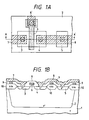
- Fig. 1A is a schematic plan view of an example of the conventional function element
- Fig. 1B is a schematic cross-sectional view along a line A-A′ in Fig. 1A.
- a drain area 3 and a source area 4 both of an n+-type semiconductor and a sub area 5 for ohmic connection of the p ⁇ well 2 with an electrode.
- a gate electrode 6 across a gate insulation film, and an n-channel MOSFET is thus formed.
- a drain electrode 7 and a source electrode 8 respectively contact with the drain area 3, and with the source and sub areas 4, 5 through contact holes formed in an insulation layer 9.
- Multi-terminal elements such as functional elements, are often used with a fixed potential at a terminal.
- the above-explained MOSFET is used with the source and sub areas thereof maintained at a same potential.
- the sub area 5 is positioned horizontally next to the source area 4 across a field insulation film 10, and said source area 4 and sub area 5 are short-circuited by the source electrode 8 connected through the contact holes.
- Such structure requires a plurality of field insulation films 10 and contact holes positioned in the horizontal direction, thus occupying a large area, and cannot achieve a sufficiently high level of integration even if a fine geometry can be realized.
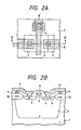
- Figs. 2A and 2B are respectively a schematic plan view and a schematic cross-sectional view along a line B-B′ in Fig. 2A.
- the source area 4 and the sub area 5 are positioned in mutually contacting manner, thereby dispensing with the field insulation film therebetween and requiring only one contact hole for said two areas, instead of one contact hole for each area.
- the horizontal positioning of the source area 4 and the sub area 5 requires an excessive surface area.
- the contact hole requires a certain large diameter for achieving sufficient short-circuiting of the source area 4 and the sub area 5, so that the design freedom of the production process is difficut to increase.
- planar CMOS transistor In the following there will be explained an example of the planar CMOS transistor.
- CMOS transistors are recently used as the elements meeting such requirements for constituting the logic circuit.
- Fig. 3 schematically illustrates the structure of an inversion logic circuit composed of conventional planar CMOS transistors.
- a p-type substrate 501 On a p-type substrate 501, there are formed an n ⁇ layer 502, a p ⁇ layer 503, a LOCOS oxide film 504, and an interlayer insulation film 505.
- the PMOS transistor includes an n+ layer 506 for obtaining the substrate potential, a p+ drain layer 507 and a p+ source layer 508, while the NMOS transistor includes an n+ source layer 509, an n+ drain layer 510 and a p+ layer 511 for obtaining the substrate potential.
- a gate oxide film 512, a gate electrode 513 for the PMOS transistor and a gate electrode 514 for the NMOS transistor There are further provided a gate oxide film 512, a gate electrode 513 for the PMOS transistor and a gate electrode 514 for the NMOS transistor.
- the drain 507 and the n+ layer 506 of the PMOS transistor are given a highest potential, while the drain 510 and the p+ layer 511 of the NMOS transistor are given a lowest potential.
- the gate electrodes 513, 514 of the PMOS and NMOS transistors are mutually connected by a metal wiring to constitute an input terminal, while the sources 508, 509 of said transistors are mutually connected by a metal wiring to constitute an output terminal, whereby an inversion logic circuit is constructed.
- the inverter function is thus realized, as the output terminal is maintained at the lowest or highest potential respectively when the highest or lowest potential is given to the input terminal.
- the device dimension is reduced by miniaturization of the gate length, contact holes and wiring width.
- the conventional structure requires formation of gate areas on the surface, and isolation of the NMOS and PMOS transistors by a LOCOS oxide film, so that the device dimension has a limitation and a further reduction in size is difficult to achieve.
- an object of the present invention is to provide a semiconductor device suitable for achieving a fine geometry and a higher level of integration.
- Another object of the present invention is to provide a semiconductor device including very small-sized functional elements.
- Still another object of the present invention is to provide a semiconductor device in which the number of electrodes is reduced and the element isolation area can be reduced in size, that the dimension of the element can be further reduced.
- Still another object of the present invention is to provide a method for producing a semiconductor device suitable for achieving a fine geometry and a higher level of integration.
- Still another object of the present invention is to provide a method for producing a semiconductor device capable of filling a fine contact hole or a fine, deep trench, thereby realizing satisfactory electrical connection.
- Still another object of the present invention is to provide a method for producing a semiconductor device, capable of significantly improving the electrical characteristics of the above-mentioned semiconductor device and of improving the production yield.
- the semiconductor device of the present invention provided with a first semiconductor area of a first conductive type, and a second semiconductor area, formed on said first semiconductor area, of a second conductive type different from said first conductive, is featured by facts that an electrode electrically connected to said first semiconductor area is formed through said second semiconductor area, and that said first and second semiconductor areas are electrically short-circuited by said electrode.
- the above-explained structure is additionally featured by facts that said second semiconductor area is a source or drain area of a field effect transistor, and that said electrode is composed of aluminum or a conductive material principally composed of aluminum.
- the field effect transistor has a buried drain area and a buried gate area, that a PMOS transistor and an NMOS transistor are formed on respective sides of said buried gate, that said second semiconductor area constitutes said buried drain area, and that said electrode reaching the drain area is provided in at least either of said PMOS and NMOS transistors.
- Said structure is further featured by a fact that said electrode is composed of aluminum or a conductive material principally composed of aluminum.
- said semiconductor device is a NOT circuit element, a NOR circuit element or a NAND circuit element.
- the semiconductor device producing method of the present invention is featured by a first step for forming an aperture in said second semiconductor area thereby exposing a part of said first semiconductor area, and a second step for depositing a conductive material in said aperture, wherein said second step is to deposit aluminum or a conductive material principally composed of aluminum into said aperture by a CVD method utilizing alkylaluminum hydride gas and hydrogen.
- Said method is further featured by a fact that said alkylaluminum hydride is dimethylaluminum hydride.
- the semiconductor device producing method of the present invention is furthermore featured by: a step for burying drain areas of PMOS transistor and an NMOS transistor in a semiconductor substrate; a step for forming an aperture so as to penetrate the junction portion between the drain area of said PMOS transistor and the drain area of said NMOS transistor; a step for forming an insulation film covering the internal surface of said aperture; a step for depositing, in said aperture, a common gate for said PMOS and NMOS transistors; and a step for forming a buried electrode reaching at least either of the buried drain area of said PMOS transistor and the buried drain area of said NMOS transistor.
- Said method is further featured by a fact that said buried electrode is formed by formation of an aperture reaching at least either of said two buried drain areas, and by selective deposition of aluminum in said aperture by a CVD method utilizing dimethylaluminum hydride and hydrogen.
- the present invention can provide a semiconductor device including very small functional elements which can be formed with necessary minimum components without unnecessary planar areas, thereby being capable of significantly reducing the layout area and adapted for achieving a fine geometry and a high level of integration.
- the present invention allows to reduce the number of electrodes and reduce the element isolation area in size, thereby further decreasing the dimension of the element.
- the present invention utilizes aluminum electrode formation by low-temperature aluminum deposition by a CVD method utilizing alkylaluminum hydride gas and hydrogen, thereby significantly improving the electrical characteristics and the production yield.
- a preferred embodiment of the present invention is constructed in the following manner.
- terminals to be used in an electrically short-circuited state are formed by forming, on a first semiconductor area of a first conductive type, a second semiconductor area of a second conductive type, and forming an electrode contacting said first semiconductor area through said second semiconductor area.
- Figs. 4A to 4D are schematic cross-sectional views showing various modes of the present invention.
- an electrode 120 which reaches a first semiconductor area 102, penetrating the center of a second semiconductor area 104.
- the electrode 120 reaches the first semiconductor area 102 through an end portion of the second semiconductor area 104.
- the electrode 120 does not sink into the first semiconductor area 102, as in the case of Fig. 4A, but merely contacts the upper surface thereof.
- 121 indicates a source electrode wiring.
- Figs. 4A to 4C do not show the sub area. Such sub area can be dispensed with if the material of the electrode 120 can make ohmic contact with the first semiconductor area 102. If necessary, a sub area 105 may be formed, as shown in Fig. 4D, at a position where the electrode contacts the first semiconductor area 102.
- the electrode 120 is preferably provided with an insulation film on a large part of the lateral wall thereof and contacts the area 104 through a silicon area exposed in said insulation film.
- Fig. 5A is a schematic cross-sectioanl view of another embodiment of the present invention
- Fig. 5B is an equivalent circuit diagram thereof.
- a p-type substrate 57 an n ⁇ diffusion layer 56, a buried drain area 51 of a PMOS transistor, a channel area 52 of the PMOS transistor, a source area 53 thereof, a gate oxide film 54 common for PMOS and NMOS transistor, a poly-silicon gate 55, an insulation film 58, a source area 201 of an NMOS transistor, a channel area 202 thereof, a buried drain area 203 thereof, a buried electrode 60 common for the drain and well of the PMOS transistor, a buried electrode 61 common for the drain and well of the NMOS transistor, source electrodes 62, 63 respectively of the PMOS and NMOS transistors, and a common gate electrode 64.
- a highest potential is given to the drain 51 and the well 52 of the PMOS transistor 30, while a lowest potential is given to the drain 203 and the well 202 of the NMOS transistor 31.
- the common gate 55 of the PMOS and NMOS transistors constitutes an input terminal, while the sources 53, 201 of the PMOS and NMOS transistors are mutually connected to constitute an output terminal, whereby an inversion logic circuit is constituted.
- the NMOS transistor 31 is rendered conductive to provide the output terminal with the lowest potential.
- the PMOS transistor 30 is rendered conductive to provide the output terminal with the highest potential. The inversion logic operation is thus realized.
- fine buried electrodes 60, 61 are buried deep into the semiconductor substrate.
- the present invention is based on a finding that a metal of satisfactory quality can be deposited with extremely good selectively by a novel CVD method to be explained later.
- the n ⁇ diffusion layer 56 was formed by ion implantation and an annealing step (Fig. 6).
- n+ drain layer 203 in the substrate 57 and the p+ drain layer 51 in the n ⁇ layer 56 were formed respectively by ion implantation and annealing (Fig. 7).
- the n ⁇ layer 52 was subsequently formed over the entire surface by CVD (Fig. 8).
- Ion implantation was conducted in an area for forming the NMOS transistor in the n ⁇ layer, followed by annealing, the form the p ⁇ layer 202 (Fig. 10).
- the p+ source area 53 and the n+ layer 59 for electrode connection were formed in the n ⁇ layer 52, and the n+ source area 201 and the p+ area 204 for electrode connection were formed in the p ⁇ layer 202, respectively by ion implantation and annealing (Fig. 11).
- the gate oxide film 54 was formed by thermal oxidation (Fig. 12).
- the interlayer insulation film 58 was deposited by CVD (Fig. 14), and the contact holes for the drains 51, 203 and the wells 52, 202 were formed by etching (Fig. 15).
- A1 was deposited in the contact holes by the above-mentioned CVD utilizing DMAH and H2, thereby forming the electrodes 60, 61 common for the drains and wells (Fig. 16).
- A1 was deposited in the contact holes by CVD, and the source electrodes 111, 112 and the gate electrode 63 were formed to complete the structure shown in Fig. 5A.
- the inversion logic circuit was formed by patterning the A1 wirings in such a manner that the source electrodes of the PMOS and NMOS transistors are mutually connected.
- the present embodiment can be constructed with only one gate electrode, and does not require an isolation area, as the gate serves to separate the PMOS and NMOS transistors. It is therefore rendered possible to reduce the number of electrodes and to reduce the isolation area in size, thereby obtaining a logic circuit of a reduced dimension.
- the source electrodes 62, 63 and the gate electrode 64 may be composed, like the electrode 120 in the aforementioned first example or the buried electrodes 60, 61 in the second example, of polycrystalline silicon, Al, W, Mo, Cu, Al-Ci, Al-Cu, Al-Ti, Al-Si-Ti, Al-Si-Cu, WSi2, MoSi2 or TiSi2, but, in consideration of the production process, they are preferably composed of aluminum or a material principally composed of aluminum such as Al-Si, Al-Cu, Al-Ti, Al-Si-Ti or Al-Si-Cu. Besides such material is preferably deposited by a depositing method to be explained in the following.
- Said method is adapted for filling an aperture with a conductive material, for forming the electrode of the above-explained structure.
- Said film forming method consists of forming a deposited film by a surface reaction on an electron donating substrate, utilizing alkylaluminum hydride gas and hydrogen gas (said method being hereinafter called Al-CVD method).
- An aluminum film of satisfactory quality can be deposited by heating the surface of the substrate in the presence of a gaseous mixture particularly consisting of monomethylaluminum hydride (MMAH) or dimethylaluminum hydride (DMAH) as the raw material gas and hydrogen as the reaction gas.
- MMAH monomethylaluminum hydride
- DMAH dimethylaluminum hydride
- the substrate surface is preferably maintained at a temperature at least equal to the decomposition temperature of alkylaluminum hydride but lower than 450°C, more preferably between 260°C and 440°C, by direct or indirect heating.
- the heating of the substrate in the above-mentioned temperature range may be achieved by direct or indirect heating, but formation of an Al film of satisfactory quality can be achieved with a high deposition speed, particularly by direct heating.
- a satisfactory film can be obtained with a deposition speed of 300 - 5000 ⁇ /min. which is higher than in the resistance heating.
- Such direct heating (substrate being heated by direct transmission of energy from the heating means) can be achieved by heating with a lamp such as a halogen lamp or a xenon lamp.
- indirect heating may be achieved for example by resistance heating, conducted by a heat generating member provided in a substrate support member, for supporting the substrate to be subjected to film deposition, provided in a film depositing space.
- This method if applied to a substrate having both an electron donating surface area and an electron non-donating surface area, allows to form single crystal of aluminum with satisfactory selectively solely on the electron donating surface area.
- Such aluminum is excellent in all the properties required for the electrode/wiring material, including a low hillock frequency and a low alloy spike frequency.
- Such Al film when employed as an electrode of a semiconductor device, provides the advantages far exeeding the concept of the conventional Al electrode and not anticipated in the prior technology.
- the Al deposited in an aperture with an electron donating surface for example an aperture formed in an insulating film and exposing the surface of a semiconductor substrate therein, has a monocrystalline structure.
- said Al-CVD method can achieve selective deposition of following metal films principally composed of aluminum, with likewise satisfactory quality.
- the electrode may be formed by selective deposition of various conductive materials such as Al-Si, Al-Ti, Al-Cu, Al-Si-Ti or Al-Si-Cu by the use of a mixed gaseous atmosphere employing, in addition to alkylaluminum hydride gas and hydrogen, a suitable combination of:
- Si-containing gas such as SiH4, Si2H6, Si3H8, Si(CH3)4, SiCl4, SiH2Cl2 or SiHCl3;
- Ti-containing gas such as TiCl4, TiBr4 or Ti(CH3)4;
- Cu-containing gas such as copper bisacetylacetonate Cu(C5H7O2)2, copper bisdipyvaloylmethanite Cu(C11H19O2)2 or copper bishexafluoroacetylacetonate Cu(C5HF6O2)2.
- said Al-CVD method is excellent in selectivity and provides satisfactory surface characteristics on the deposited film, there can be obtained a metal film suitable and widely usable for the wirings of a semiconductor device, by employing a non-selective film forming method in a next deposition step to form a metal film composed solely or principally of aluminum not only on the selectively deposited aluminum film mentioned above but also on the SiO2 insulation film.
- metal films examples include combinations of selectively deposited Al, Al-Si, Al-Ti, Al-Cu, Al-Si-Ti or Al-Si-Cu and non-selectively deposited Al, Al-Si, Al-Ti, Al-Cu, Al-Si-Ti or Al-Si-Cu.
- Said non-selective film deposition may be achieved by CVD other than the aforementioned Al-CVD, or by sputtering.
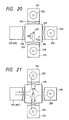
- Figs. 18 to 20 schematically illustrate a continuous metal film forming apparatus suitable for executing the film forming method explained above.
- said apparatus is composed of a loading chamber 311, a CVD reaction chamber (first film forming chamber) 312, an Rf etching chamber 313, a sputtering chamber (second film forming chamber) 314 and an unloading chamber 315, which are rendered sealable from the external atmosphere and mutually communicatable by means of gate valves 310a - 310f and can be respectively made vacuum or reduced in pressure by vacuum systems 316a - 316e.
- the loading chamber 311 is used for eliminating the atmosphere of substrate and replacing it with H2 prior to the deposition, in order to improve the throughput.
- the next CVD reaction chamber 312, for selective deposition onto the substrate under normal or reduced pressure is provided therein with a substrate holder 318 with a resistance heater 317 for heating the substrate surface subjected to film formation at least within a temperature range of 200° - 450°C, and receives the raw material gas such as of alkylaluminum hydride, which is gasified by bubbling with hydrogen in a bubbler 319-1, through a raw material gas supply line 319, and hydrogen as the reaction gas through a gas line 319′.
- the raw material gas such as of alkylaluminum hydride
- the Rf etching chamber 313, for cleaning (etching) of the substrate surface in Ar atmosphere after the selective deposition, is provided therein with a substrate holder 320 capable of heating the substrate at least within a range of 100° - 250°C and an Rf etching electrode line 321, and is connected to an Ar gas supply line 322.
- the sputtering chamber 314, for non-selective deposition of a metal film by sputtering in Ar atmosphere, is provided therein with a substrate holder 323 to be heated at least within a range of 200° - 250°C and a target electrode 324 for mounting a sputtering target 324a, and is connected to an Ar gas supply line 325.
- the final unloading chamber 315, for adjustment of the substrate after metal film deposition and prior to the exposure to the external atmosphere, is designed to be capable of replacing the atmosphere with N2.
- Fig. 19 shows another example of the continuous metal film forming apparatus, wherein same components as those in Fig. 18 are represented by same numbers.
- the apparatus in Fig. 19 is different from that in Fig. 18 in that the substrate surface is directly heated by halogen lamps 330, and, for this purpose, the substrate holder 312 is provided with projections 331 for supporting the substrate in a floating state.
- Direct heating of the substrate surface with such structure further increases the deposition speed as explained before.
- the continuous metal film forming apparatus of the above-explained structure is equivalent, in practice, to a structure shown in Fig. 20, in which the loading chamber 311, CVD reaction chamber 312, Rf etching chamber 313, sputtering chamber 314 and unloading chamber 315 are mutually combined by a transport chamber 326.
- the loading chamber 311 serves also as the chamber 315.
- an arm 327 constituting transport means, rotatable in both directions A-A and extendable and retractable in direction B-B, whereby the substrate can be transferred in succession from the loading chamber 311 to the CVD reaction chamber 312, Rf etching chamber 313, sputtering chamber 314, and finally to the unloading chamber 315 without exposure to the external atmosphere, as indicated by arrows in Fig. 21.
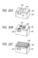
- Fig. 22 illustrates the film forming procedure for forming the electrodes and wirings according to the present invention, in schematic perspective views.
- a semiconductor substrate with an insulating film having apertures therein is placed in the film forming chamber, and the surface thereof is maintained for example at 250° - 450°C.
- Thermal CVD conducted in a mixed atmosphere of DMAH gas as alkylaluminum hydride and hydrogen gas causes selective deposition of Al on the semiconductor exposed in the apertures.
- DMAH gas alkylaluminum hydride and hydrogen gas
- a metal film principally composed of Al for example Al-Si
- Si-containing gas introduction for example of Si-containing gas
- a substrate consisting for example of a monocrystalline silicon wafer bearing thereon grooves of different sizes, and covered by an insulation film except for the bottoms of said grooves.
- Fig. 22A schematically shows a part of said substrate, wherein shown are a monocrystalline silicon substrate 401 constituting a conductive substrate; a thermal silicon oxide film 402 constituting an insulation film; apertures 403, 404 of different sizes; and a groove 410.
- Al film constituting a first wiring layer, on the substrate is conducted in the following manner, with the apparatus shown in Fig. 19.
- the above-explained substrate is placed in the loading chamber 311, in which a hydrogen atmosphere is established by introduction of hydrogen as explained before. Then the reaction chamber 312 is evacuated by the vacuum system 316b approximately to 1 x 10 ⁇ 8 Torr, though Al film formation is still possible with a higher pressure.
- DMAH gas obtained by bubbling is supplied from the gas line 319, utilizing H2 as the carrier gas.
- reaction gas is introduced from the second gas line 319′, and the interior of the reaction chamber 312 is maintained at a predetermined pressure, by the adjustment of an unrepresented slow leak valve.
- a typical pressure is about 1.5 Torr.
- DMAH is introduced into the reaction chamber from the DMAH line, with a total pressure of about 1.5 Torr and a DMAH partial pressure of about 5.0 x 10 ⁇ 3 Torr. Then the halogen lamps 330 are energized to directly heat the wafer, thereby causing selective Al deposition.
- the DMAH supply is interrupted. Said deposition time is so selected that the Al film on Si (monocrystalline silicon substrate 1) becomes equally thick as SiO2 (thermal silicon oxide film 2), and can be experimentally determined in advance.
- the substrate surface is heated to ca. 270°C by direct heating, and the procedure explained above causes selective deposition of an Al film 405 in the aperture, as shown in Fig. 22B.
- the foregoing is called a first film forming step for forming an electrode in an aperture.
- the CVD reaction chamber 312 is evacuated, by the vacuum system 316b, to a pressure not exceeding 5 x 10 ⁇ 3 Torr.
- the Rf etching chamber 313 is evacuated to a pressure not exceeding 5 x 10 ⁇ 6 Torr.
- the gate valve 310c is opened, then the substrate is moved from the CVD reaction chamber 312 to the Rf etching chamber 313 by the transport means, and said gate valve is closed.
- the Rf etching chamber 313 is evacuated to a pressure not exceeding 10 ⁇ 6 Torr, and is then maintained in argon atmosphere of 10 ⁇ 1 - 10 ⁇ 3 Torr by argon supply from the supply line 322.
- the substrate holder 320 is maintained at ca. 200°C, and an Rf power of 100 W is supplied to the Rf etching electrode 321 for about 60 seconds to generate an argon discharge in said chamber 313, whereby the substrate surface is etched with argon ions and the unnecessary surfacial layer of the CVD deposition film can be eliminated.
- the etch depth in this case is about 100 ⁇ , corresponding to the oxide film.
- Said surface etching, of the CVD deposition film, conducted in the Rf etching chamber may be dispensed with since said surfacial layer is free from oxygen etc. as the substrate is transported in vacuum.
- the Rf etching chamber 313 may serve for varying the temperature within a short time if the temperature is significantly different between the CVD reaction chamber 312 and the sputtering chamber 314.
- the argon supply is terminated, and the Rf etching chamber 313 is evacuated to 5 x 10 ⁇ 6 Torr. Then the sputtering chamber is also evacuated to 5 x 10 ⁇ 6 Torr or lower, and the gate valve 310d is opened. The substrate is transferred from the Rf etching chamber 313 to the sputtering chamber 314 by the transport means, and said gate valve 310d is closed.
- the sputtering chamber is maintained at argon atmosphere of 10 ⁇ 1 - 10 ⁇ 3 Torr as in the Rf etching chamber 313, and the substrate holder 323 is maintained at 200° - 250°C.
- Argon discharge is induced by a DC power of 5 - 10 kW to scrape the target of Al or Al-Si (Si: 0.5%) with argon ions, thereby depositing Al or Al-Si onto the substrate with a deposition speed of ca. 10000 ⁇ /min.
- This is a non-selective deposition step, and is called a second film forming step for forming wirings connected to the electrodes.
- the argon supply and the DC power application are terminated.
- the loading chamber 311 is evacuated to a pressure of 5 x 10 ⁇ 3 Torr or lower, then the gate valve 310e is opened and the substrate is moved. After the gate valve 310e is closed, the loading chamber 311 is supplied with nitrogen gas to the atmospheric pressure. Subsequently the gate valve 310f is opened and the substrate is taken out.
- the second Al film deposition step explained above forms an Al film 406 on the SiO2 film 402, as shown in Fig. 22C.
- the Al film in the apertures obtained in a substrate surface temperature range of 260° - 440°C, showed satisfactory characteristics, with no carbon content, a resistivity of 2.8 - 3.4 ⁇ cm, a reflectance of 90 - 95%, a hillock ( ⁇ 1 ⁇ m) density of 0 - 10 cm ⁇ 2, and an almost zero spike formation (frequency of destruction of 0.15 ⁇ m junction).
- the quality of the Al film in the apertures were deteriorated, with a reflectance of 60% or lower, a hillock ( ⁇ 1 ⁇ m) density of 10 - 104 cm ⁇ 2 and an alloy spike formation of 0 - 30%.
- Said method can be advantageously applied to the grooves composed of the materials explained in the following.
- the Al film formation was conducted on the following substrates (samples) under the same conditions as in the Al film formation on the above-mentioned samples 1-1.
- Samples 1-2 were prepared by forming, on monocrystalline silicon constituting a first substrate surface material, a silicon oxide film constituting a second substrate surface material by means of CVD method, and forming grooves by a photolithographic process to locally expose the surface of monocrystalline silicon in the bottoms of said grooves.
- the thermal SiO2 film was 8000 ⁇ thick, and the exposed areas of monocrystalline silicon were sizes from 0.25 x 0.25 ⁇ m to 100 x 100 ⁇ m, with a groove depth of 2 ⁇ m. (Such samples will hereinafter be represented as "CVD SiO2 (or simply SiO2)/monocrystalline silicon”.)
- a sample 1-3 of boron-doped oxide film formed by normal pressure CVD (hereinafter written as BSG)/monocrystalline silicon; a sample 1-4 of phosphor-doped oxide film formed by normal pressure CVD (PSG)/monocrystalline silicon; a smaple 1-5 of boron- and phosphor-doped oxide film formed by normal pressure CVD (BSPG)/monocrystalline silicon; a sample 1-6 of nitride film formed by plasma CVD (P-SiN)/monocrystalline silicon; a sample 1-7 of thermal nitride film (T-Sin)/monocrystalline silicon; a sample 1-8 of nitride film formed by low pressure CVD (LP-SiN)/monocrystalline silicon; and a sample 1-9 of nitride film formed by ECR (ECR-SiN)/monocrystalline silicon.
- BSG normal pressure CVD
- PSG normal pressure CVD
- BSPG normal pressure CVD
- samples 1-11 to 1-179 were prepared by taking all the combinations of the first surface materials of 18 kinds and the second surface materials of 9 kinds shown in the following. (It is to be noted that the sample numbers 1-10, 20, 30, 40, 50, 60, 70, 80, 90, 100, 110, 120, 130, 140, 150, 160 and 170 are lacking.)
- the first surface materials employed were monocrystalline silicon (mono-Si), polycrystalline silicon (poly-Si), amorphous silicon (a-Si), tungsten (W), molybdenum (Mo), tantalum (Ta), tungsten silicide (WSi), titanium silicide (TiSi), aluminum (Al), aluminum silicon (Al-Si), titanium aluminum (Al-Ti), titanium nitride (Ti-N), copper (Cu), aluminum silicon copper (Al-Si-Cu), aluminum palladium (Al-Pd), titanium (Ti), molybdenum silicide (Mo-Si), and tantalum silicide (T
- the second substrate surface materials employed were T-SiO2, SiO2, BSG, PSG, BPSG, P-SiN, T-SiN, LP-SiN and ECR-SiN. In all these samples, there could be obtained satisfactory Al films comparable to those in the aforementioned samples 1-1.
- the Al was non-selectively deposited by sputtering on the substrates subjected to the selective Al deposition as explained above, and was then patterned.
- Such deposited film is effective for three-dimensional connections of buried wirings.
- the Al film obtained by sputtering and the selectively deposited Al film in the apertures showed electrically and mechanically satisfactory contact, because of the improved surface state of the Al film in the apertures.
- Fig. 23A is a schematic plan view of a MOSFET of said first embodiment
- Fig. 23B is a schematic cross-sectional view along a line X-X′ in Fig. 23A.
- a silicon substrate 101 of n-type semiconductor There are shown a silicon substrate 101 of n-type semiconductor; a p ⁇ well 102; a drain area 103 of n+ type formed in the p ⁇ well 102; a source area 104 formed similarly to the drain area 103; a p+ sub area 105 for making ohmic contact between the p ⁇ well 102 and the source electrode; a polycrystalline silicon gate electrode 106; a gate electrode wiring 106′ connected to said gate electrode 106 by a through-hole; an insulation film 109 of silicon oxide; and a field insulation film 110 with bird's beak formed by selective oxidation.
- An electrode 120 constituting the most characteristic structure of the present invention, is composed of monocrystalline aluminum, and penetrates the contact hole in the insulation layer 109 and the source area 104 and reaches the sub area 105 buried in the p ⁇ well 102.
- a source electrode wiring 121 formed on the insulation layer 109 and the electrode 120, is composed of aluminum.
- a drain electrode 122 buried in the contact hole on the drain area 103, is composed of monocrystalline aluminum. There is also provided a drain electrode wiring 123.
- the contact hole is formed in the insulation layer 109 on the drain area 103 by a known process as shown in Fig. 24D (hole opening step), and aluminum was deposited by the above-mentioned Al-CVD method.
- the device was completed then by forming the source electrode wiring 121 and the drain electrode wiring 123 respectively on said electrode 102 and on the drain area 103 by sputtering as shown in Fig. 24E (Al wiring step).
- the present invention allows to constitute a MOSFET, which is to be used with the source area and the sub area thereof in an electrically shortcircuited state, with necessary minimum components and without any unnecessary surface area.
- Fig. 25A illustrates a second embodiment of the present invention.
- the present invention is applied to a CMOS inverter circuit.
- the production method will not be explained as it is basically same as that of the first embodiment.
- Fig. 25B is a circuit diagram of the present embodiment
- Fig. 25C is a similar device obtained by the prior art, for the purpose of comparison.
- the layout area of the device can be significantly reduced by the use of the electrode structure of the present invention in the connecting part of the source area and the sub area in the inverter circuit.
- FIG. 26A and 26B A third embodiment of the present invention is illustrated in Figs. 26A and 26B, and in a circuit diagram in Fig. 26C.
- the producing process of the present embodiment will not be explained as it is basically same as that of the foregoing first embodiment.
- the present third embodiment also provides a CMOS inverter, but is different from the second embodiment in that the MOS transistors have a vertical structure.
- the electrode structure of the present invention is even more effective for reducing the layout area in a circuit employing vertical MOS transistors.
- FIG. 27A and 27B A fourth embodiment of the present invention is illustrated in Figs. 27A and 27B, and shown in a circuit diagram in Fig. 27C.
- the producing process of the present embodiment will not be explained, as it is basically same as that of the foregoing first embodiment.
- the present invention is applied to a NAND circuit composed again with vertical MOS transistors.
- the electrode structure of the present invention is effective, also in this embodiment, for reducing the layout area.
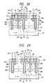
- Fig. 28 is a schematic cross-sectional view of a NOR circuit element constituting a fifth embodiment of the present invention.
- Fig. 28 there are shown polysilicon gates 205, 207 respectively of PMOS and NMOS transistors; gate insulation films 206, 208; a p+ drain layer 209 of the PMOS transistor; an n+ source layer 210 of the NMOS transistor; and electrodes 211, 212, 213, 214 respectively for the drain 209, source 210, and polysilicon gates 205, 207.
- the source 53 of the PMOS transistor and the sources 201, 210 of the NMOS transistor are mutually connected.
- These two electrodes 61, 211 are formed by selective deposition by the aforementioned Al-CVD method.
- the structure shown in Fig. 28 can be formed by steps similar to those shown in Figs. 6 to 17.
- a first input terminal 215 of the NOR circuit is connected to the gate 207 of the NMOS transistor and the gate 205 of the PMOS transistor.
- a second input terminal 216 of the NOR circuit is connected to the common gate 55 of the NMOS and PMOS transistors.
- the present device functions in the following manner.
- the first input terminal 215 receives a voltage equal to or larger than V th of the NMOS transistor, for example a highest potential and the second input terminal 216 receives a voltage euqal to or lower than [highest potential + V th of PMOS transistor], for example a lowest potential
- a channel is formed below the NMOS transistor, whereby the drain 203 and the source 210 thereof are connected and the output terminal 217 is maintained at the lowest potential.
- the p+ layer 101 and the source area 53 are connected through the channel, but the source 53 is not connected to the power supply since a channel is not formed between the drain 209 and the p+ layer 51.
- the drain 203 and the source 201 of the NMOS transistor are connected through the channel, whereby the output terminal is maintained at the lowest potential.
- the drain 209 and the p+ layer 51 of the PMOS transistor are connected through the channel, but the source 53 is not connected to the power supply, since a channel is not formed between the source 53 and the p+ layer 51 of the PMOS transistor.
- the first and second input terminals 215, 216 both receive a voltage equal to or higher than V th of the NMOS transistor, for example the highest potential, a channel is formed below the NMOS transistor, whereby the drain 203 is connected with the sources 201, 210 through said channel and the output terminal 217 is maintained at the lowest potential.
- the source 53 is not connected to the power supply, since a channel is not formed below the PMOS transistor.
- the first and second input terminals 215, 216 both receive a voltage equal to or lower than [highest potential + V th of PMOS transistor], for example the lowest potential, a channel is formed below the PMOS transistor, whereby the source 53 is connected to the drain 209 through the p+ layer 51 and the output terminal 217 is maintained at the highest potential. In this state the sources 201, 210 are not connected to the power supply, since a channel is not formed below the NMOS transistor.
- the NOR function is achieved as explained above, since the output terminal is maintained at the highest potential only when the first and second input termianls are given the lowest potential and at the lowest potential in other combinations of the input potentials.
- the present embodiment can reduce the number of electrode and the dimension of the element, as in the example shown in Fig. 5.
- Fig. 29 is a schematic cross-sectional view of a NAND circuit device constituting a sixth embodiment of the present invention.
- a p+ source layer 218 of the PMOS transistor and an n+ drain layer 219 of the NMOS transistor.
- a buried electrode 60 reaching a p+ drain layer 51 is formed at the PMOS side, and an electrode 220 for the n+ drain 219 is formed at the NMOS side.
- Said electrode 220 is also formed by selective aluminum deposition utilizing DMAH and hydrogen.
- the structure shown in Fig. 29 can be prepared by steps similar to those in Figs. 6 to 17.
- a first input terminal 221 of the NAND circuit is connected to the gate 207 of the NMOS transistor and the gate 205 of the PMOS transistor.
- a second input terminal 222 of the NAND circuit is connected to the common gate 55 of the NMOS and PMOS transistors.
- the device of the present embodiment functions in the following manner.
- the first input terminal 221 receives a voltage equal to or higher than V th of the NMOS transistor, for example a highest potential
- the second input terminal 222 receives a voltage equal to or lower than [highest potential + V th of PMOS transistor], for example a lowest potential
- a channel is formed below the PMOS transistor whereby the drain 51 and the source 53 thereof are connected and an output terminal 223 is maintained at the highest potential.
- the n+ layer 203 is connected with the drain 219 through the channel, but the source 201 is not connected to the power source since a channel is not formed between the source 201 and the n+ layer 203.
- the drain 51 and the source 218 of the PMOS transistor are connected through the channel whereby the output terminal 223 is maintained at the highest potential.
- the source 201 is not connected to the power source since a channel is not formed between the drain 219 and the n+ layer 203 of the NMOS transistor.
- the first and second input terminals both receive a voltage equal to or lower than [highest potential + V th of PMOS transistor], for example the lowest potential, a channel is formed below the PMOS transistor, whereby the drain 51 is connected with the source 53, 218 through said channel and the output terminal 223 is maintained at the highest potential.
- the source 201 is not connected to the power source, since a channel is not formed below the NMOS transistor. Then, when the first and second input terminals both receive a voltage equal to or higher than V th of the NMOS transistor, for example the highest potential, a channel is formed below the NMOS transistor, whereby the drain 219 is connected with the source 200 through the n+ layer 203 and the output terminal is maintained at the lowest potential. In this state the sources 53, 218 are not connected to the power source, since a channel is not formed below the PMOS transistor.
- the NAND function is thus achieved, as the output terminal is maintained at the lowest potential only when the first and second input terminals are given the highest potential, but is maintained at the highest potential at other combinations of the input potentials.
- this NAND circuit device is provided with a reduced number of electrodes and can therefore reduce the dimension of the device.
- the present invention allows to obtain a semiconductor device provided with very small functional elements, which can be constructed by necessary minimum components without any unnecessary surface area, thereby being capable of significantly reducing the layout area and adapted for achieving a fine geometry and a high level of integration.
Applications Claiming Priority (4)
| Application Number | Priority Date | Filing Date | Title |
|---|---|---|---|
| JP13961890 | 1990-05-31 | ||
| JP139618/90 | 1990-05-31 | ||
| JP208145/90 | 1990-08-08 | ||
| JP20814590 | 1990-08-08 |
Publications (3)
| Publication Number | Publication Date |
|---|---|
| EP0459771A2 true EP0459771A2 (de) | 1991-12-04 |
| EP0459771A3 EP0459771A3 (en) | 1992-02-05 |
| EP0459771B1 EP0459771B1 (de) | 1997-08-27 |
Family
ID=26472367
Family Applications (1)
| Application Number | Title | Priority Date | Filing Date |
|---|---|---|---|
| EP91304828A Expired - Lifetime EP0459771B1 (de) | 1990-05-31 | 1991-05-29 | Elektrode für einen vertikalen Feldeffekttransistor und Verfahren zu deren Herstellung |
Country Status (10)
| Country | Link |
|---|---|
| US (2) | US5378914A (de) |
| EP (1) | EP0459771B1 (de) |
| JP (1) | JP3067263B2 (de) |
| CN (1) | CN1052343C (de) |
| AT (1) | ATE157482T1 (de) |
| DE (1) | DE69127402T2 (de) |
| DK (1) | DK0459771T3 (de) |
| ES (1) | ES2104668T3 (de) |
| GR (1) | GR3025139T3 (de) |
| MY (1) | MY107475A (de) |
Cited By (2)
| Publication number | Priority date | Publication date | Assignee | Title |
|---|---|---|---|---|
| EP0657930A2 (de) * | 1993-12-07 | 1995-06-14 | Siemens Aktiengesellschaft | Integrierte Schaltungsstruktur mit mindestens einem CMOS-NAND-Gatter und Verfahren zu deren Herstellung |
| US7786530B2 (en) | 2002-07-15 | 2010-08-31 | Infineon Technologies Ag | Vertical field-effect transistor |
Families Citing this family (51)
| Publication number | Priority date | Publication date | Assignee | Title |
|---|---|---|---|---|
| JPH0661266A (ja) * | 1992-08-06 | 1994-03-04 | Mitsubishi Electric Corp | 半導体装置とその製造方法 |
| JPH07130871A (ja) * | 1993-06-28 | 1995-05-19 | Toshiba Corp | 半導体記憶装置 |
| DE4340967C1 (de) * | 1993-12-01 | 1994-10-27 | Siemens Ag | Verfahren zur Herstellung einer integrierten Schaltungsanordnung mit mindestens einem MOS-Transistor |
| JP3338178B2 (ja) * | 1994-05-30 | 2002-10-28 | 株式会社東芝 | 半導体装置およびその製造方法 |
| US5510287A (en) * | 1994-11-01 | 1996-04-23 | Taiwan Semiconductor Manuf. Company | Method of making vertical channel mask ROM |
| US5455190A (en) * | 1994-12-07 | 1995-10-03 | United Microelectronics Corporation | Method of making a vertical channel device using buried source techniques |
| JP3303601B2 (ja) * | 1995-05-19 | 2002-07-22 | 日産自動車株式会社 | 溝型半導体装置 |
| GB9512089D0 (en) * | 1995-06-14 | 1995-08-09 | Evans Jonathan L | Semiconductor device fabrication |
| US6917083B1 (en) * | 1995-07-27 | 2005-07-12 | Micron Technology, Inc. | Local ground and VCC connection in an SRAM cell |
| EP0864178A4 (de) * | 1995-10-02 | 2001-10-10 | Siliconix Inc | Grabengate-mosfet mit integraler temperatur-erkennungsdiode |
| JP3141769B2 (ja) * | 1996-02-13 | 2001-03-05 | 富士電機株式会社 | 絶縁ゲート型サイリスタ及びその製造方法 |
| US5929476A (en) * | 1996-06-21 | 1999-07-27 | Prall; Kirk | Semiconductor-on-insulator transistor and memory circuitry employing semiconductor-on-insulator transistors |
| JP3397057B2 (ja) * | 1996-11-01 | 2003-04-14 | 日産自動車株式会社 | 半導体装置 |
| JPH10290007A (ja) * | 1997-04-14 | 1998-10-27 | Sharp Corp | 半導体装置およびその製造方法 |
| US5909618A (en) * | 1997-07-08 | 1999-06-01 | Micron Technology, Inc. | Method of making memory cell with vertical transistor and buried word and body lines |
| US6150687A (en) * | 1997-07-08 | 2000-11-21 | Micron Technology, Inc. | Memory cell having a vertical transistor with buried source/drain and dual gates |
| US6222271B1 (en) | 1997-07-15 | 2001-04-24 | Micron Technology, Inc. | Method of using hydrogen gas in sputter deposition of aluminum-containing films and aluminum-containing films derived therefrom |
| US5969423A (en) * | 1997-07-15 | 1999-10-19 | Micron Technology, Inc. | Aluminum-containing films derived from using hydrogen and oxygen gas in sputter deposition |
| US6528837B2 (en) * | 1997-10-06 | 2003-03-04 | Micron Technology, Inc. | Circuit and method for an open bit line memory cell with a vertical transistor and trench plate trench capacitor |
| US6066869A (en) * | 1997-10-06 | 2000-05-23 | Micron Technology, Inc. | Circuit and method for a folded bit line memory cell with vertical transistor and trench capacitor |
| JPH11186194A (ja) * | 1997-12-19 | 1999-07-09 | Nec Corp | 半導体装置の製造方法 |
| US6100123A (en) | 1998-01-20 | 2000-08-08 | International Business Machines Corporation | Pillar CMOS structure |
| US6025225A (en) * | 1998-01-22 | 2000-02-15 | Micron Technology, Inc. | Circuits with a trench capacitor having micro-roughened semiconductor surfaces and methods for forming the same |
| US6020239A (en) * | 1998-01-28 | 2000-02-01 | International Business Machines Corporation | Pillar transistor incorporating a body contact |
| US6246083B1 (en) * | 1998-02-24 | 2001-06-12 | Micron Technology, Inc. | Vertical gain cell and array for a dynamic random access memory |
| US6124729A (en) | 1998-02-27 | 2000-09-26 | Micron Technology, Inc. | Field programmable logic arrays with vertical transistors |
| US6057238A (en) * | 1998-03-20 | 2000-05-02 | Micron Technology, Inc. | Method of using hydrogen and oxygen gas in sputter deposition of aluminum-containing films and aluminum-containing films derived therefrom |
| US6208164B1 (en) | 1998-08-04 | 2001-03-27 | Micron Technology, Inc. | Programmable logic array with vertical transistors |
| US6204123B1 (en) * | 1998-10-30 | 2001-03-20 | Sony Corporation | Vertical floating gate transistor with epitaxial channel |
| US6194741B1 (en) * | 1998-11-03 | 2001-02-27 | International Rectifier Corp. | MOSgated trench type power semiconductor with silicon carbide substrate and increased gate breakdown voltage and reduced on-resistance |
| WO2000052760A1 (en) * | 1999-03-01 | 2000-09-08 | General Semiconductor, Inc. | Trench dmos transistor structure having a low resistance path to a drain contact located on an upper surface |
| US6500744B2 (en) | 1999-09-02 | 2002-12-31 | Micron Technology, Inc. | Methods of forming DRAM assemblies, transistor devices, and openings in substrates |
| JP3899231B2 (ja) * | 2000-12-18 | 2007-03-28 | 株式会社豊田中央研究所 | 半導体装置 |
| US6551881B1 (en) * | 2001-10-01 | 2003-04-22 | Koninklijke Philips Electronics N.V. | Self-aligned dual-oxide umosfet device and a method of fabricating same |
| US6838723B2 (en) * | 2002-08-29 | 2005-01-04 | Micron Technology, Inc. | Merged MOS-bipolar capacitor memory cell |
| US7224024B2 (en) * | 2002-08-29 | 2007-05-29 | Micron Technology, Inc. | Single transistor vertical memory gain cell |
| JP4028333B2 (ja) * | 2002-09-02 | 2007-12-26 | 株式会社東芝 | 半導体装置 |
| US6804142B2 (en) * | 2002-11-12 | 2004-10-12 | Micron Technology, Inc. | 6F2 3-transistor DRAM gain cell |
| US7838875B1 (en) | 2003-01-22 | 2010-11-23 | Tsang Dean Z | Metal transistor device |
| US6747306B1 (en) | 2003-02-04 | 2004-06-08 | International Business Machines Corporation | Vertical gate conductor with buried contact layer for increased contact landing area |
| US6956256B2 (en) * | 2003-03-04 | 2005-10-18 | Micron Technology Inc. | Vertical gain cell |
| US6838332B1 (en) * | 2003-08-15 | 2005-01-04 | Freescale Semiconductor, Inc. | Method for forming a semiconductor device having electrical contact from opposite sides |
| DE102006030631B4 (de) * | 2006-07-03 | 2011-01-05 | Infineon Technologies Austria Ag | Halbleiterbauelementanordnung mit einem Leistungsbauelement und einem Logikbauelement |
| KR100949890B1 (ko) * | 2007-12-11 | 2010-03-25 | 주식회사 하이닉스반도체 | 반도체 소자 및 그 제조 방법 |
| KR100922557B1 (ko) * | 2007-12-27 | 2009-10-21 | 주식회사 동부하이텍 | Cmos 트랜지스터 및 그 제조 방법 |
| JP5493669B2 (ja) * | 2009-10-07 | 2014-05-14 | ソニー株式会社 | 固体撮像装置、撮像装置、および固体撮像装置の製造方法 |
| CN102403256B (zh) * | 2010-09-08 | 2014-02-26 | 上海华虹宏力半导体制造有限公司 | 赝埋层及制造方法、深孔接触及三极管 |
| JP5075959B2 (ja) * | 2010-09-14 | 2012-11-21 | 株式会社東芝 | 抵抗変化メモリ |
| US8704297B1 (en) * | 2012-10-12 | 2014-04-22 | Force Mos Technology Co., Ltd. | Trench metal oxide semiconductor field effect transistor with multiple trenched source-body contacts for reducing gate charge |
| CN103137646A (zh) * | 2013-03-15 | 2013-06-05 | 中国科学院微电子研究所 | 用于双极型阻变存储器交叉阵列集成方式的选通器件单元 |
| US9397094B2 (en) | 2014-09-25 | 2016-07-19 | International Business Machines Corporation | Semiconductor structure with an L-shaped bottom plate |
Citations (7)
| Publication number | Priority date | Publication date | Assignee | Title |
|---|---|---|---|---|
| GB2055247A (en) * | 1979-07-28 | 1981-02-25 | Itt | Method of fabricating VMOS transistors |
| JPS5935463A (ja) * | 1982-08-24 | 1984-02-27 | Toshiba Corp | 相補型mos半導体装置及びその製造方法 |
| JPS618969A (ja) * | 1984-06-25 | 1986-01-16 | Nec Corp | 半導体集積回路装置 |
| JPS61136682A (ja) * | 1984-12-05 | 1986-06-24 | Nec Corp | レ−ザcvd方法 |
| EP0284065A2 (de) * | 1987-03-26 | 1988-09-28 | Nec Corporation | Komplementäre Feldeffekttransistorstruktur |
| JPS63288057A (ja) * | 1987-05-20 | 1988-11-25 | Sanyo Electric Co Ltd | Cmos半導体装置 |
| JPH01244646A (ja) * | 1988-03-25 | 1989-09-29 | Mitsubishi Electric Corp | 半導体装置の製造方法 |
Family Cites Families (16)
| Publication number | Priority date | Publication date | Assignee | Title |
|---|---|---|---|---|
| JPS57162457A (en) * | 1981-03-31 | 1982-10-06 | Fujitsu Ltd | Semiconductor memory unit |
| JPS60148147A (ja) * | 1984-01-13 | 1985-08-05 | Nec Corp | 半導体装置 |
| US4768076A (en) * | 1984-09-14 | 1988-08-30 | Hitachi, Ltd. | Recrystallized CMOS with different crystal planes |
| JPH0793282B2 (ja) * | 1985-04-15 | 1995-10-09 | 株式会社日立製作所 | 半導体装置の製造方法 |
| JPS6252969A (ja) * | 1985-08-30 | 1987-03-07 | Nippon Texas Instr Kk | 絶縁ゲ−ト型電界効果半導体装置 |
| US4740826A (en) * | 1985-09-25 | 1988-04-26 | Texas Instruments Incorporated | Vertical inverter |
| US4845051A (en) * | 1987-10-29 | 1989-07-04 | Siliconix Incorporated | Buried gate JFET |
| JPH01194437A (ja) * | 1988-01-29 | 1989-08-04 | Mitsubishi Electric Corp | 半導体装置 |
| JPH01244546A (ja) * | 1988-03-25 | 1989-09-28 | Hokuriku Nippon Denki Software Kk | データ処理装置の機能診断方式 |
| US4898835A (en) * | 1988-10-12 | 1990-02-06 | Sgs-Thomson Microelectronics, Inc. | Single mask totally self-aligned power MOSFET cell fabrication process |
| US5016070A (en) * | 1989-06-30 | 1991-05-14 | Texas Instruments Incorporated | Stacked CMOS sRAM with vertical transistors and cross-coupled capacitors |
| JP2721023B2 (ja) * | 1989-09-26 | 1998-03-04 | キヤノン株式会社 | 堆積膜形成法 |
| EP0420594B1 (de) * | 1989-09-26 | 1996-04-17 | Canon Kabushiki Kaisha | Verfahren zur Herstellung von einer abgeschiedenen Metallschicht, die Aluminium als Hauptkomponent enthält, mit Anwendung von Alkalimetallaluminiumhydride |
| US5077228A (en) * | 1989-12-01 | 1991-12-31 | Texas Instruments Incorporated | Process for simultaneous formation of trench contact and vertical transistor gate and structure |
| US5010386A (en) * | 1989-12-26 | 1991-04-23 | Texas Instruments Incorporated | Insulator separated vertical CMOS |
| DE69120446T2 (de) * | 1990-02-19 | 1996-11-14 | Canon Kk | Verfahren zum Herstellen von abgeschiedener Metallschicht, die Aluminium als Hauptkomponente enthält, mit Anwendung von Alkylaluminiumhydrid |
-
1991
- 1991-05-27 MY MYPI91000927A patent/MY107475A/en unknown
- 1991-05-29 DK DK91304828.6T patent/DK0459771T3/da active
- 1991-05-29 DE DE69127402T patent/DE69127402T2/de not_active Expired - Fee Related
- 1991-05-29 AT AT91304828T patent/ATE157482T1/de not_active IP Right Cessation
- 1991-05-29 EP EP91304828A patent/EP0459771B1/de not_active Expired - Lifetime
- 1991-05-29 ES ES91304828T patent/ES2104668T3/es not_active Expired - Lifetime
- 1991-05-31 CN CN91104371.3A patent/CN1052343C/zh not_active Expired - Fee Related
- 1991-05-31 JP JP03129771A patent/JP3067263B2/ja not_active Expired - Fee Related
-
1992
- 1992-12-24 US US07/997,135 patent/US5378914A/en not_active Expired - Fee Related
-
1994
- 1994-12-05 US US08/352,050 patent/US5583075A/en not_active Expired - Lifetime
-
1997
- 1997-10-22 GR GR970402771T patent/GR3025139T3/el unknown
Patent Citations (7)
| Publication number | Priority date | Publication date | Assignee | Title |
|---|---|---|---|---|
| GB2055247A (en) * | 1979-07-28 | 1981-02-25 | Itt | Method of fabricating VMOS transistors |
| JPS5935463A (ja) * | 1982-08-24 | 1984-02-27 | Toshiba Corp | 相補型mos半導体装置及びその製造方法 |
| JPS618969A (ja) * | 1984-06-25 | 1986-01-16 | Nec Corp | 半導体集積回路装置 |
| JPS61136682A (ja) * | 1984-12-05 | 1986-06-24 | Nec Corp | レ−ザcvd方法 |
| EP0284065A2 (de) * | 1987-03-26 | 1988-09-28 | Nec Corporation | Komplementäre Feldeffekttransistorstruktur |
| JPS63288057A (ja) * | 1987-05-20 | 1988-11-25 | Sanyo Electric Co Ltd | Cmos半導体装置 |
| JPH01244646A (ja) * | 1988-03-25 | 1989-09-29 | Mitsubishi Electric Corp | 半導体装置の製造方法 |
Non-Patent Citations (5)
| Title |
|---|
| PATENT ABSTRACTS OF JAPAN vol. 10, no. 150 (E-408)31 May 1986 & JP-A-61 008 969 ( NIPPON DENKI K.K. ) 16 January 1986 * |
| PATENT ABSTRACTS OF JAPAN vol. 10, no. 328 (C-383)7 November 1986 & JP-A-61 136 682 ( NEC CORP ) 24 June 1986 * |
| PATENT ABSTRACTS OF JAPAN vol. 13, no. 117 (E-731)22 March 1989 & JP-A-63 288 057 ( SANYO ELECTRIC CO LTD ) 25 November 1988 * |
| PATENT ABSTRACTS OF JAPAN vol. 13, no. 581 (E-865)21 December 1989 & JP-A-1 244 646 ( MITSUBISHI ELECTRIC CORP ) 29 September 1989 * |
| PATENT ABSTRACTS OF JAPAN vol. 8, no. 123 (E-249)8 June 1984 & JP-A-59 035 463 ( TOKYO SHIBAURA DENKI K.K. ) 27 February 1984 * |
Cited By (3)
| Publication number | Priority date | Publication date | Assignee | Title |
|---|---|---|---|---|
| EP0657930A2 (de) * | 1993-12-07 | 1995-06-14 | Siemens Aktiengesellschaft | Integrierte Schaltungsstruktur mit mindestens einem CMOS-NAND-Gatter und Verfahren zu deren Herstellung |
| EP0657930A3 (de) * | 1993-12-07 | 1998-01-07 | Siemens Aktiengesellschaft | Integrierte Schaltungsstruktur mit mindestens einem CMOS-NAND-Gatter und Verfahren zu deren Herstellung |
| US7786530B2 (en) | 2002-07-15 | 2010-08-31 | Infineon Technologies Ag | Vertical field-effect transistor |
Also Published As
| Publication number | Publication date |
|---|---|
| CN1052343C (zh) | 2000-05-10 |
| DE69127402T2 (de) | 1998-01-02 |
| ATE157482T1 (de) | 1997-09-15 |
| ES2104668T3 (es) | 1997-10-16 |
| US5378914A (en) | 1995-01-03 |
| GR3025139T3 (en) | 1998-02-27 |
| JPH04226075A (ja) | 1992-08-14 |
| JP3067263B2 (ja) | 2000-07-17 |
| DK0459771T3 (da) | 1997-09-22 |
| CN1057736A (zh) | 1992-01-08 |
| EP0459771B1 (de) | 1997-08-27 |
| EP0459771A3 (en) | 1992-02-05 |
| MY107475A (en) | 1995-12-30 |
| US5583075A (en) | 1996-12-10 |
| DE69127402D1 (de) | 1997-10-02 |
Similar Documents
| Publication | Publication Date | Title |
|---|---|---|
| EP0459771B1 (de) | Elektrode für einen vertikalen Feldeffekttransistor und Verfahren zu deren Herstellung | |
| US5218232A (en) | Semiconductor device having two-level wiring | |
| US5404046A (en) | Flat semiconductor wiring layers | |
| US5665630A (en) | Device separation structure and semiconductor device improved in wiring structure | |
| US5599741A (en) | Method for making semiconductor device with metal deposited on electron donating surface of gate electrode | |
| US5483104A (en) | Self-aligning contact and interconnect structure | |
| US6287964B1 (en) | Method for forming a metallization layer of a semiconductor device | |
| KR100360396B1 (ko) | 반도체소자의 콘택 구조체 형성방법 | |
| KR100281307B1 (ko) | 선택에피택셜성장을 사용한 반도체장치의 제조방법 | |
| KR900008387B1 (ko) | 반도체장치 제조방법 | |
| JPH09237838A (ja) | 金属配線構造及びその形成方法 | |
| US6010955A (en) | Electrical connection forming process for semiconductor devices | |
| US6218223B1 (en) | Process for producing electrode for semiconductor element and semiconductor device having the electrode | |
| US6746952B2 (en) | Diffusion barrier layer for semiconductor wafer fabrication | |
| JPH10294294A (ja) | 半導体デバイスの金属配線の形成方法 | |
| JP2790362B2 (ja) | 半導体装置 | |
| JP3061891B2 (ja) | 半導体装置の製造方法 | |
| KR950006481B1 (ko) | 반도체장치 및 그 제조방법 | |
| JP3067264B2 (ja) | 半導体装置 | |
| CN117199072B (zh) | 一种半导体结构及其制作方法 | |
| JP2895167B2 (ja) | 半導体装置およびその製造方法 | |
| JPH0563200A (ja) | 半導体装置 | |
| US6117768A (en) | Void-free tungsten-plug contact for ULSI interconnection | |
| JP2786313B2 (ja) | 半導体装置およびその製造方法 | |
| JPH0529248A (ja) | 半導体装置およびその製造方法 |
Legal Events
| Date | Code | Title | Description |
|---|---|---|---|
| PUAI | Public reference made under article 153(3) epc to a published international application that has entered the european phase |
Free format text: ORIGINAL CODE: 0009012 |
|
| AK | Designated contracting states |
Kind code of ref document: A2 Designated state(s): AT BE CH DE DK ES FR GB GR IT LI LU NL SE |
|
| PUAL | Search report despatched |
Free format text: ORIGINAL CODE: 0009013 |
|
| AK | Designated contracting states |
Kind code of ref document: A3 Designated state(s): AT BE CH DE DK ES FR GB GR IT LI LU NL SE |
|
| 17P | Request for examination filed |
Effective date: 19920623 |
|
| 17Q | First examination report despatched |
Effective date: 19941031 |
|
| GRAG | Despatch of communication of intention to grant |
Free format text: ORIGINAL CODE: EPIDOS AGRA |
|
| GRAH | Despatch of communication of intention to grant a patent |
Free format text: ORIGINAL CODE: EPIDOS IGRA |
|
| GRAH | Despatch of communication of intention to grant a patent |
Free format text: ORIGINAL CODE: EPIDOS IGRA |
|
| GRAA | (expected) grant |
Free format text: ORIGINAL CODE: 0009210 |
|
| AK | Designated contracting states |
Kind code of ref document: B1 Designated state(s): AT BE CH DE DK ES FR GB GR IT LI LU NL SE |
|
| REF | Corresponds to: |
Ref document number: 157482 Country of ref document: AT Date of ref document: 19970915 Kind code of ref document: T |
|
| REG | Reference to a national code |
Ref country code: CH Ref legal event code: EP |
|
| REG | Reference to a national code |
Ref country code: DK Ref legal event code: T3 |
|
| REG | Reference to a national code |
Ref country code: CH Ref legal event code: NV Representative=s name: BOVARD AG PATENTANWAELTE |
|
| REF | Corresponds to: |
Ref document number: 69127402 Country of ref document: DE Date of ref document: 19971002 |
|
| REG | Reference to a national code |
Ref country code: ES Ref legal event code: FG2A Ref document number: 2104668 Country of ref document: ES Kind code of ref document: T3 |
|
| ET | Fr: translation filed | ||
| ITF | It: translation for a ep patent filed |
Owner name: SOCIETA' ITALIANA BREVETTI S.P.A. |
|
| REG | Reference to a national code |
Ref country code: GR Ref legal event code: FG4A Free format text: 3025139 |
|
| PLBE | No opposition filed within time limit |
Free format text: ORIGINAL CODE: 0009261 |
|
| STAA | Information on the status of an ep patent application or granted ep patent |
Free format text: STATUS: NO OPPOSITION FILED WITHIN TIME LIMIT |
|
| 26N | No opposition filed | ||
| REG | Reference to a national code |
Ref country code: GB Ref legal event code: IF02 |
|
| PGFP | Annual fee paid to national office [announced via postgrant information from national office to epo] |
Ref country code: ES Payment date: 20030505 Year of fee payment: 13 |
|
| PGFP | Annual fee paid to national office [announced via postgrant information from national office to epo] |
Ref country code: CH Payment date: 20030512 Year of fee payment: 13 Ref country code: AT Payment date: 20030512 Year of fee payment: 13 |
|
| PGFP | Annual fee paid to national office [announced via postgrant information from national office to epo] |
Ref country code: SE Payment date: 20030513 Year of fee payment: 13 |
|
| PGFP | Annual fee paid to national office [announced via postgrant information from national office to epo] |
Ref country code: DK Payment date: 20030521 Year of fee payment: 13 |
|
| PGFP | Annual fee paid to national office [announced via postgrant information from national office to epo] |
Ref country code: GR Payment date: 20030523 Year of fee payment: 13 |
|
| PGFP | Annual fee paid to national office [announced via postgrant information from national office to epo] |
Ref country code: FR Payment date: 20030526 Year of fee payment: 13 |
|
| PGFP | Annual fee paid to national office [announced via postgrant information from national office to epo] |
Ref country code: BE Payment date: 20030611 Year of fee payment: 13 |
|
| PGFP | Annual fee paid to national office [announced via postgrant information from national office to epo] |
Ref country code: LU Payment date: 20030703 Year of fee payment: 13 |
|
| PG25 | Lapsed in a contracting state [announced via postgrant information from national office to epo] |
Ref country code: LU Free format text: LAPSE BECAUSE OF NON-PAYMENT OF DUE FEES Effective date: 20040529 Ref country code: AT Free format text: LAPSE BECAUSE OF NON-PAYMENT OF DUE FEES Effective date: 20040529 |
|
| PG25 | Lapsed in a contracting state [announced via postgrant information from national office to epo] |
Ref country code: SE Free format text: LAPSE BECAUSE OF NON-PAYMENT OF DUE FEES Effective date: 20040530 |
|
| PG25 | Lapsed in a contracting state [announced via postgrant information from national office to epo] |
Ref country code: LI Free format text: LAPSE BECAUSE OF NON-PAYMENT OF DUE FEES Effective date: 20040531 Ref country code: ES Free format text: LAPSE BECAUSE OF NON-PAYMENT OF DUE FEES Effective date: 20040531 Ref country code: CH Free format text: LAPSE BECAUSE OF NON-PAYMENT OF DUE FEES Effective date: 20040531 Ref country code: BE Free format text: LAPSE BECAUSE OF NON-PAYMENT OF DUE FEES Effective date: 20040531 |
|
| PG25 | Lapsed in a contracting state [announced via postgrant information from national office to epo] |
Ref country code: DK Free format text: LAPSE BECAUSE OF NON-PAYMENT OF DUE FEES Effective date: 20040601 |
|
| BERE | Be: lapsed |
Owner name: *CANON K.K. Effective date: 20040531 |
|
| PG25 | Lapsed in a contracting state [announced via postgrant information from national office to epo] |
Ref country code: GR Free format text: LAPSE BECAUSE OF NON-PAYMENT OF DUE FEES Effective date: 20041203 |
|
| EUG | Se: european patent has lapsed | ||
| REG | Reference to a national code |
Ref country code: DK Ref legal event code: EBP |
|
| REG | Reference to a national code |
Ref country code: CH Ref legal event code: PL |
|
| PG25 | Lapsed in a contracting state [announced via postgrant information from national office to epo] |
Ref country code: FR Free format text: LAPSE BECAUSE OF NON-PAYMENT OF DUE FEES Effective date: 20050131 |
|
| REG | Reference to a national code |
Ref country code: FR Ref legal event code: ST |
|
| PGFP | Annual fee paid to national office [announced via postgrant information from national office to epo] |
Ref country code: NL Payment date: 20050513 Year of fee payment: 15 |
|
| PGFP | Annual fee paid to national office [announced via postgrant information from national office to epo] |
Ref country code: GB Payment date: 20050516 Year of fee payment: 15 |
|
| PG25 | Lapsed in a contracting state [announced via postgrant information from national office to epo] |
Ref country code: IT Free format text: LAPSE BECAUSE OF NON-PAYMENT OF DUE FEES Effective date: 20050529 |
|
| PGFP | Annual fee paid to national office [announced via postgrant information from national office to epo] |
Ref country code: DE Payment date: 20050720 Year of fee payment: 15 |
|
| REG | Reference to a national code |
Ref country code: ES Ref legal event code: FD2A Effective date: 20040531 |
|
| PG25 | Lapsed in a contracting state [announced via postgrant information from national office to epo] |
Ref country code: GB Free format text: LAPSE BECAUSE OF NON-PAYMENT OF DUE FEES Effective date: 20060529 |
|
| PG25 | Lapsed in a contracting state [announced via postgrant information from national office to epo] |
Ref country code: NL Free format text: LAPSE BECAUSE OF NON-PAYMENT OF DUE FEES Effective date: 20061201 Ref country code: DE Free format text: LAPSE BECAUSE OF NON-PAYMENT OF DUE FEES Effective date: 20061201 |
|
| GBPC | Gb: european patent ceased through non-payment of renewal fee |
Effective date: 20060529 |
|
| NLV4 | Nl: lapsed or anulled due to non-payment of the annual fee |
Effective date: 20061201 |