EP0098775B1 - Verfahren zur Realisierung von einem Feldoxide für eine integrierte Schaltung - Google Patents
Verfahren zur Realisierung von einem Feldoxide für eine integrierte Schaltung Download PDFInfo
- Publication number
- EP0098775B1 EP0098775B1 EP83401332A EP83401332A EP0098775B1 EP 0098775 B1 EP0098775 B1 EP 0098775B1 EP 83401332 A EP83401332 A EP 83401332A EP 83401332 A EP83401332 A EP 83401332A EP 0098775 B1 EP0098775 B1 EP 0098775B1
- Authority
- EP
- European Patent Office
- Prior art keywords
- substrate
- etching
- resin
- layer
- region
- Prior art date
- Legal status (The legal status is an assumption and is not a legal conclusion. Google has not performed a legal analysis and makes no representation as to the accuracy of the status listed.)
- Expired
Links
Images

Classifications
-
- H10P95/064—
-
- H10W10/0121—
-
- H10W10/0124—
-
- H10W10/0126—
-
- H10W10/13—
-
- Y—GENERAL TAGGING OF NEW TECHNOLOGICAL DEVELOPMENTS; GENERAL TAGGING OF CROSS-SECTIONAL TECHNOLOGIES SPANNING OVER SEVERAL SECTIONS OF THE IPC; TECHNICAL SUBJECTS COVERED BY FORMER USPC CROSS-REFERENCE ART COLLECTIONS [XRACs] AND DIGESTS
- Y10—TECHNICAL SUBJECTS COVERED BY FORMER USPC
- Y10S—TECHNICAL SUBJECTS COVERED BY FORMER USPC CROSS-REFERENCE ART COLLECTIONS [XRACs] AND DIGESTS
- Y10S438/00—Semiconductor device manufacturing: process
- Y10S438/978—Semiconductor device manufacturing: process forming tapered edges on substrate or adjacent layers
Definitions
- the present invention relates to a process for producing the field oxide of an integrated circuit. It applies in particular in the field of manufacturing MOS integrated circuits.
- LOCOS One of the main processes for producing known field oxide is that generally called the “LOCOS • process.
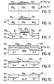
- Figures 1 to 4 show the different stages of this LOCOS process.
- the first step of this process consists, as shown in FIG. 1, in thermally growing on a silicon substrate 2, for example of type P, a layer of silicon oxide 4, of small thickness, that is to say -to say of the order of 0.07 microns, then to deposit a layer of silicon nitride 6 on the oxide layer 4, generally having a thickness close to 0.08 microns.
- a resin mask 8 has been produced on the region 6a of the silicon nitride layer 6, situated above the region of the substrate in which the elementary component of the integrated circuit will be produced subsequently, for example on the central region of the silicon nitride layer as shown in FIG. 1, an etching of the silicon nitride layer 6 is carried out for example by a plasma attack.
- FIG. 2 The structure thus obtained is shown in FIG. 2.
- ions are implanted, through the oxide layer 4, giving a doping of the same type as that of the substrate.
- This ion implantation makes it possible to obtain, in the substrate 2, two lateral regions 10 and 12, for example of the P + type in the case of a P-type substrate and of an implantation of boron ions.
- This implantation is carried out with a dose of 2.10 12 atoms / cm 2 and at an energy of 140 keV, for example.
- the resin mask 8 is then eliminated.
- the next step consists in producing the field oxide by thermal oxidation of the silicon, the active zones where it is desired to produce the elementary components being masked by the region 6a of the layer of silicon nitride 6 during this oxidation. Two lateral regions 14 and 16 of silica are thus obtained, having a thickness generally between 0.6 and 0.8 micrometers.
- This process ends by eliminating the region 6a of the layer of silicon nitride 6 and the region of the oxide layer 4, situated above the region of the substrate 2 in which the component will be produced subsequently. This elimination is done for example by a chemical attack. The structure thus obtained is shown in FIG. 4.
- This process for producing the field oxide of an integrated circuit has a number of drawbacks.
- the thermal oxidation step so as to obtain the regions 14 and 16 in silica is a long and tedious step.
- this thermal oxidation is carried out at a relatively low temperature, of the order of 900 ° C., for approximately 10 hours.
- This method of producing the field oxide also has the major drawback of limiting the integration density of the integrated circuits. Indeed, the field oxide, produced by this process, has a significant lateral extension, referenced L in FIG. 4.
- the subject of the present invention is precisely a process for producing the field oxide of an integrated circuit which makes it possible to remedy these various drawbacks.
- This process makes it possible in particular to avoid prolonged heat treatment, to decrease the dose of the ions to be implanted and, to increase the density of integration of the integrated circuits.
- said second etching of the resin layer and of the oxide layer is carried out with identical attack speeds. for resin and insulation.
- this second etching is done by reactive ion etching using a gas mixture containing trifluoromethane (CHF 3 ) and oxygen in adequate proportions. It is also possible to use other gases such as a mixture of carbon tetrafluoride (CF 4 ) and oxygen, or else sulfur hexafluoride (SF 6 ).
- CHF 3 trifluoromethane
- SF 6 sulfur hexafluoride
- this protective layer produced in particular from silicon nitride, makes it possible to protect the surface of the semiconductor substrate from the various etchings, thus avoiding the formation of defects in the active areas of the substrate and the contamination thereof.
- the etching step d) is carried out by an anisotropic etching process such as, for example, reactive ion etching.
- an anisotropic etching process such as, for example, reactive ion etching.
- an etching is carried out on a slope of the first region of the substrate (20) during step d).
- a sloping etching is carried out using a sloping profile of the resin mask produced during step b, and an anisotropic reactive ion etching .
- a thermal oxidation of the substrate is carried out, for example over a thickness of the order of 0.05 to 0.1 ⁇ m .
- a thermal oxide layer in fact makes it possible to ensure a good quality interface between the substrate and the insulating layer subsequently deposited.
- the first step of the method according to the invention consists in depositing on a doped semiconductor substrate 20.
- a protective layer 22 made for example of nitride of silicon.
- This protective layer 22 makes it possible to avoid any subsequent contamination of the substrate 20 during the various stages of the process according to the invention.
- This protective layer 22, deposited for example by the chemical vapor deposition technique, at low pressure or not, has for example a thickness of 0.1 microns.
- a resin mask 24 is produced on the protective layer 22 so as to mask only the region 22a of this layer 22, located on the region 20a of the semiconductor substrate 20, in which will be subsequently produced the active component, then an anisotropic etching of the protective layer 22 is carried out, for example by means of reactive ion etching with SF 6 (sulfur hexafluoride). This etching eliminates the regions 22b of the protective layer 22, located above the regions 20b of the semiconductor substrate 20, in which the field oxide according to the invention will be produced. The structure obtained, after this engraving, is shown in FIG. 6.
- an anisotropic etching of the regions 20b of the substrate is preferably carried out over a height h of about 0.8 microns. This etching is done for example by reactive ion etching with SF s .
- the resin layer 24 can be subjected, before etching the protective layer and the substrate, to a heat treatment, that is to say to a heating of the order of 120 ° C. , or to the action of an oxygen plasma so as to effect a slight attack on the resin.
- This heat treatment where this slight attack makes it possible to obtain an inclined profile of the resin mask 24, causing, during the anisotropic etching of the substrate, an inclined profile of the region 20a of the substrate.
- the slope of this profile will depend on the slope of the profile of the resin mask 24 and the respective attack speeds of the resin and the substrate during the etching of the latter.
- the next step of the method according to the invention consists, always using the same mask 24, disposed on the region 22a of the protective layer 22, in implanting ions, in the remaining regions 20b of the substrate, these ions giving a doping of the same type as that of the substrate.
- this implantation can be carried out with boron ions at an energy of 50 keV and at a dose of 10 12 atoms / cm 2 . This implantation makes it possible to obtain lateral regions 28 and 30, for example of the P + type.
- a thermal oxidation of the substrate (not shown) is carried out on a thickness of 0.05 ⁇ rn for example. Such an oxidation can be carried out at 900 ° C for 1 hour.
- an insulating layer 32 is deposited on the entire substrate 20 and on the region 22a of the layer of silicon nitride. remaining, for example by the chemical vapor deposition technique, at low pressure or not, an insulating layer 32, made for example of silica. This insulating layer 32 has for example a thickness of 1 micron.
- this silica layer 32 by deposition and not by thermal oxidation makes it possible to use, during ion implantation, a lesser quantity of ions than that used during the processes for producing field oxide of the prior art, since the diffusion of ions into the substrate is completely avoided. Furthermore, this makes it possible to completely eliminate the lateral extensions of the oxide and therefore to increase the integration density of the integrated circuits.
- the next step of the process consists in covering the oxide layer 32 with a resin layer 34.
- This resin layer 34 which can be made of a resin such as the resins commonly used in photolithography has for example a thickness of 1 , 5 J, Lm.
- the resin layer 34 can be subjected to a heat treatment, for example to heating at a temperature of 200 ° C. for 1/2 hour, in order to obtain good spreading of this resin layer and therefore a surface.
- plane 36 as shown in FIG. 8.
- an etching of the resin layer 34 and of the oxide layer 32 is carried out simultaneously with identical attack speeds for the resin and the oxide until the region 32a of the oxide layer 32 is completely eliminated. , located above region 20a of the substrate; the end of etching control is done by any known means.
- the structure obtained is shown in FIG. 9.
- This etching can be carried out for example by a mixture of tri or tetrafluoromethane (CHF 3 , CF 4 ) and oxygen; fluorinated compounds used for etching the oxide and oxygen for etching the resin.
- sulfur hexafluoride (SF 6 ) can also be used.
- the last step of the method according to the invention consists in eliminating the region 22a of the remaining silicon nitride layer, for example by etching said region by means of chemical etching.
- the final structure obtained is shown in Figure 10.
Landscapes
- Drying Of Semiconductors (AREA)
- Element Separation (AREA)
- Local Oxidation Of Silicon (AREA)
Claims (12)
Applications Claiming Priority (2)
| Application Number | Priority Date | Filing Date | Title |
|---|---|---|---|
| FR8211570 | 1982-07-01 | ||
| FR8211570A FR2529714A1 (fr) | 1982-07-01 | 1982-07-01 | Procede de realisation de l'oxyde de champ d'un circuit integre |
Publications (3)
| Publication Number | Publication Date |
|---|---|
| EP0098775A2 EP0098775A2 (de) | 1984-01-18 |
| EP0098775A3 EP0098775A3 (en) | 1984-02-22 |
| EP0098775B1 true EP0098775B1 (de) | 1987-09-09 |
Family
ID=9275585
Family Applications (1)
| Application Number | Title | Priority Date | Filing Date |
|---|---|---|---|
| EP83401332A Expired EP0098775B1 (de) | 1982-07-01 | 1983-06-28 | Verfahren zur Realisierung von einem Feldoxide für eine integrierte Schaltung |
Country Status (5)
| Country | Link |
|---|---|
| US (1) | US4455193A (de) |
| EP (1) | EP0098775B1 (de) |
| JP (1) | JPS5913334A (de) |
| DE (1) | DE3373592D1 (de) |
| FR (1) | FR2529714A1 (de) |
Families Citing this family (373)
| Publication number | Priority date | Publication date | Assignee | Title |
|---|---|---|---|---|
| JPS59161069A (ja) * | 1983-03-04 | 1984-09-11 | Oki Electric Ind Co Ltd | Mos型半導体装置の製造方法 |
| DE3329074A1 (de) * | 1983-08-11 | 1985-02-28 | Siemens AG, 1000 Berlin und 8000 München | Verhinderung der oxidationsmitteldiffusion bei der herstellung von halbleiterschichtanordnungen |
| US4566889A (en) * | 1983-10-28 | 1986-01-28 | Chevron Research Company | Process of fabricating a portion of an optical fiber capable of reflecting predetermined wavelength bands of light |
| US4511430A (en) * | 1984-01-30 | 1985-04-16 | International Business Machines Corporation | Control of etch rate ratio of SiO2 /photoresist for quartz planarization etch back process |
| JPS60223165A (ja) * | 1984-04-19 | 1985-11-07 | Toshiba Corp | 半導体装置の製造方法 |
| JPS614240A (ja) * | 1984-06-18 | 1986-01-10 | Toshiba Corp | 半導体装置の製造方法 |
| US4687543A (en) * | 1986-02-21 | 1987-08-18 | Tegal Corporation | Selective plasma etching during formation of integrated circuitry |
| US4689869A (en) * | 1986-04-07 | 1987-09-01 | International Business Machines Corporation | Fabrication of insulated gate gallium arsenide FET with self-aligned source/drain and submicron channel length |
| FR2599892B1 (fr) * | 1986-06-10 | 1988-08-26 | Schiltz Andre | Procede d'aplanissement d'un substrat semiconducteur revetu d'une couche dielectrique |
| US4726879A (en) * | 1986-09-08 | 1988-02-23 | International Business Machines Corporation | RIE process for etching silicon isolation trenches and polycides with vertical surfaces |
| FR2610141B1 (fr) * | 1987-01-26 | 1990-01-19 | Commissariat Energie Atomique | Circuit integre cmos et procede de fabrication de zones d'isolation electrique dans ce circuit |
| FR2610140B1 (fr) * | 1987-01-26 | 1990-04-20 | Commissariat Energie Atomique | Circuit integre cmos et procede de fabrication de ses zones d'isolation electrique |
| NL8700541A (nl) * | 1987-03-06 | 1988-10-03 | Philips Nv | Werkwijze voor het vervaardigen van een halfgeleiderinrichting waarbij een plak silicium plaatselijk wordt voorzien van veldoxidegebieden. |
| US4764248A (en) * | 1987-04-13 | 1988-08-16 | Cypress Semiconductor Corporation | Rapid thermal nitridized oxide locos process |
| IT1225636B (it) * | 1988-12-15 | 1990-11-22 | Sgs Thomson Microelectronics | Metodo di scavo con profilo di fondo arrotondato per strutture di isolamento incassate nel silicio |
| KR100479172B1 (ko) * | 1997-05-22 | 2005-07-12 | 삼성전자주식회사 | 선택적다결정실리콘산화법을이용한필드산화막형성방법 |
| US10378106B2 (en) | 2008-11-14 | 2019-08-13 | Asm Ip Holding B.V. | Method of forming insulation film by modified PEALD |
| US9394608B2 (en) | 2009-04-06 | 2016-07-19 | Asm America, Inc. | Semiconductor processing reactor and components thereof |
| US8802201B2 (en) | 2009-08-14 | 2014-08-12 | Asm America, Inc. | Systems and methods for thin-film deposition of metal oxides using excited nitrogen-oxygen species |
| US9312155B2 (en) | 2011-06-06 | 2016-04-12 | Asm Japan K.K. | High-throughput semiconductor-processing apparatus equipped with multiple dual-chamber modules |
| US10364496B2 (en) | 2011-06-27 | 2019-07-30 | Asm Ip Holding B.V. | Dual section module having shared and unshared mass flow controllers |
| US10854498B2 (en) | 2011-07-15 | 2020-12-01 | Asm Ip Holding B.V. | Wafer-supporting device and method for producing same |
| US20130023129A1 (en) | 2011-07-20 | 2013-01-24 | Asm America, Inc. | Pressure transmitter for a semiconductor processing environment |
| US9017481B1 (en) | 2011-10-28 | 2015-04-28 | Asm America, Inc. | Process feed management for semiconductor substrate processing |
| US9659799B2 (en) | 2012-08-28 | 2017-05-23 | Asm Ip Holding B.V. | Systems and methods for dynamic semiconductor process scheduling |
| US10714315B2 (en) | 2012-10-12 | 2020-07-14 | Asm Ip Holdings B.V. | Semiconductor reaction chamber showerhead |
| US20160376700A1 (en) | 2013-02-01 | 2016-12-29 | Asm Ip Holding B.V. | System for treatment of deposition reactor |
| US9484191B2 (en) | 2013-03-08 | 2016-11-01 | Asm Ip Holding B.V. | Pulsed remote plasma method and system |
| US9589770B2 (en) | 2013-03-08 | 2017-03-07 | Asm Ip Holding B.V. | Method and systems for in-situ formation of intermediate reactive species |
| US9240412B2 (en) | 2013-09-27 | 2016-01-19 | Asm Ip Holding B.V. | Semiconductor structure and device and methods of forming same using selective epitaxial process |
| US10683571B2 (en) | 2014-02-25 | 2020-06-16 | Asm Ip Holding B.V. | Gas supply manifold and method of supplying gases to chamber using same |
| US10167557B2 (en) | 2014-03-18 | 2019-01-01 | Asm Ip Holding B.V. | Gas distribution system, reactor including the system, and methods of using the same |
| US11015245B2 (en) | 2014-03-19 | 2021-05-25 | Asm Ip Holding B.V. | Gas-phase reactor and system having exhaust plenum and components thereof |
| US10858737B2 (en) | 2014-07-28 | 2020-12-08 | Asm Ip Holding B.V. | Showerhead assembly and components thereof |
| US9890456B2 (en) | 2014-08-21 | 2018-02-13 | Asm Ip Holding B.V. | Method and system for in situ formation of gas-phase compounds |
| US9657845B2 (en) | 2014-10-07 | 2017-05-23 | Asm Ip Holding B.V. | Variable conductance gas distribution apparatus and method |
| US10941490B2 (en) | 2014-10-07 | 2021-03-09 | Asm Ip Holding B.V. | Multiple temperature range susceptor, assembly, reactor and system including the susceptor, and methods of using the same |
| KR102263121B1 (ko) | 2014-12-22 | 2021-06-09 | 에이에스엠 아이피 홀딩 비.브이. | 반도체 소자 및 그 제조 방법 |
| US10529542B2 (en) | 2015-03-11 | 2020-01-07 | Asm Ip Holdings B.V. | Cross-flow reactor and method |
| US10276355B2 (en) | 2015-03-12 | 2019-04-30 | Asm Ip Holding B.V. | Multi-zone reactor, system including the reactor, and method of using the same |
| US10458018B2 (en) | 2015-06-26 | 2019-10-29 | Asm Ip Holding B.V. | Structures including metal carbide material, devices including the structures, and methods of forming same |
| US10600673B2 (en) | 2015-07-07 | 2020-03-24 | Asm Ip Holding B.V. | Magnetic susceptor to baseplate seal |
| US9960072B2 (en) | 2015-09-29 | 2018-05-01 | Asm Ip Holding B.V. | Variable adjustment for precise matching of multiple chamber cavity housings |
| US10211308B2 (en) | 2015-10-21 | 2019-02-19 | Asm Ip Holding B.V. | NbMC layers |
| US10322384B2 (en) | 2015-11-09 | 2019-06-18 | Asm Ip Holding B.V. | Counter flow mixer for process chamber |
| US11139308B2 (en) | 2015-12-29 | 2021-10-05 | Asm Ip Holding B.V. | Atomic layer deposition of III-V compounds to form V-NAND devices |
| US10529554B2 (en) | 2016-02-19 | 2020-01-07 | Asm Ip Holding B.V. | Method for forming silicon nitride film selectively on sidewalls or flat surfaces of trenches |
| US10468251B2 (en) | 2016-02-19 | 2019-11-05 | Asm Ip Holding B.V. | Method for forming spacers using silicon nitride film for spacer-defined multiple patterning |
| US10501866B2 (en) | 2016-03-09 | 2019-12-10 | Asm Ip Holding B.V. | Gas distribution apparatus for improved film uniformity in an epitaxial system |
| US10343920B2 (en) | 2016-03-18 | 2019-07-09 | Asm Ip Holding B.V. | Aligned carbon nanotubes |
| US9892913B2 (en) | 2016-03-24 | 2018-02-13 | Asm Ip Holding B.V. | Radial and thickness control via biased multi-port injection settings |
| US10190213B2 (en) | 2016-04-21 | 2019-01-29 | Asm Ip Holding B.V. | Deposition of metal borides |
| US10865475B2 (en) | 2016-04-21 | 2020-12-15 | Asm Ip Holding B.V. | Deposition of metal borides and silicides |
| US10367080B2 (en) | 2016-05-02 | 2019-07-30 | Asm Ip Holding B.V. | Method of forming a germanium oxynitride film |
| US10032628B2 (en) | 2016-05-02 | 2018-07-24 | Asm Ip Holding B.V. | Source/drain performance through conformal solid state doping |
| KR102592471B1 (ko) | 2016-05-17 | 2023-10-20 | 에이에스엠 아이피 홀딩 비.브이. | 금속 배선 형성 방법 및 이를 이용한 반도체 장치의 제조 방법 |
| US11453943B2 (en) | 2016-05-25 | 2022-09-27 | Asm Ip Holding B.V. | Method for forming carbon-containing silicon/metal oxide or nitride film by ALD using silicon precursor and hydrocarbon precursor |
| US10388509B2 (en) | 2016-06-28 | 2019-08-20 | Asm Ip Holding B.V. | Formation of epitaxial layers via dislocation filtering |
| US10612137B2 (en) | 2016-07-08 | 2020-04-07 | Asm Ip Holdings B.V. | Organic reactants for atomic layer deposition |
| US9859151B1 (en) | 2016-07-08 | 2018-01-02 | Asm Ip Holding B.V. | Selective film deposition method to form air gaps |
| US10714385B2 (en) | 2016-07-19 | 2020-07-14 | Asm Ip Holding B.V. | Selective deposition of tungsten |
| KR102354490B1 (ko) | 2016-07-27 | 2022-01-21 | 에이에스엠 아이피 홀딩 비.브이. | 기판 처리 방법 |
| KR102532607B1 (ko) | 2016-07-28 | 2023-05-15 | 에이에스엠 아이피 홀딩 비.브이. | 기판 가공 장치 및 그 동작 방법 |
| US9812320B1 (en) | 2016-07-28 | 2017-11-07 | Asm Ip Holding B.V. | Method and apparatus for filling a gap |
| US9887082B1 (en) | 2016-07-28 | 2018-02-06 | Asm Ip Holding B.V. | Method and apparatus for filling a gap |
| US10395919B2 (en) | 2016-07-28 | 2019-08-27 | Asm Ip Holding B.V. | Method and apparatus for filling a gap |
| KR102613349B1 (ko) | 2016-08-25 | 2023-12-14 | 에이에스엠 아이피 홀딩 비.브이. | 배기 장치 및 이를 이용한 기판 가공 장치와 박막 제조 방법 |
| US10410943B2 (en) | 2016-10-13 | 2019-09-10 | Asm Ip Holding B.V. | Method for passivating a surface of a semiconductor and related systems |
| US10643826B2 (en) | 2016-10-26 | 2020-05-05 | Asm Ip Holdings B.V. | Methods for thermally calibrating reaction chambers |
| US11532757B2 (en) | 2016-10-27 | 2022-12-20 | Asm Ip Holding B.V. | Deposition of charge trapping layers |
| US10229833B2 (en) | 2016-11-01 | 2019-03-12 | Asm Ip Holding B.V. | Methods for forming a transition metal nitride film on a substrate by atomic layer deposition and related semiconductor device structures |
| US10435790B2 (en) | 2016-11-01 | 2019-10-08 | Asm Ip Holding B.V. | Method of subatmospheric plasma-enhanced ALD using capacitively coupled electrodes with narrow gap |
| US10643904B2 (en) | 2016-11-01 | 2020-05-05 | Asm Ip Holdings B.V. | Methods for forming a semiconductor device and related semiconductor device structures |
| US10714350B2 (en) | 2016-11-01 | 2020-07-14 | ASM IP Holdings, B.V. | Methods for forming a transition metal niobium nitride film on a substrate by atomic layer deposition and related semiconductor device structures |
| US10134757B2 (en) | 2016-11-07 | 2018-11-20 | Asm Ip Holding B.V. | Method of processing a substrate and a device manufactured by using the method |
| KR102546317B1 (ko) | 2016-11-15 | 2023-06-21 | 에이에스엠 아이피 홀딩 비.브이. | 기체 공급 유닛 및 이를 포함하는 기판 처리 장치 |
| US10340135B2 (en) | 2016-11-28 | 2019-07-02 | Asm Ip Holding B.V. | Method of topologically restricted plasma-enhanced cyclic deposition of silicon or metal nitride |
| KR102762543B1 (ko) | 2016-12-14 | 2025-02-05 | 에이에스엠 아이피 홀딩 비.브이. | 기판 처리 장치 |
| US11581186B2 (en) | 2016-12-15 | 2023-02-14 | Asm Ip Holding B.V. | Sequential infiltration synthesis apparatus |
| US11447861B2 (en) | 2016-12-15 | 2022-09-20 | Asm Ip Holding B.V. | Sequential infiltration synthesis apparatus and a method of forming a patterned structure |
| KR102700194B1 (ko) | 2016-12-19 | 2024-08-28 | 에이에스엠 아이피 홀딩 비.브이. | 기판 처리 장치 |
| US10269558B2 (en) | 2016-12-22 | 2019-04-23 | Asm Ip Holding B.V. | Method of forming a structure on a substrate |
| US10867788B2 (en) | 2016-12-28 | 2020-12-15 | Asm Ip Holding B.V. | Method of forming a structure on a substrate |
| US11390950B2 (en) | 2017-01-10 | 2022-07-19 | Asm Ip Holding B.V. | Reactor system and method to reduce residue buildup during a film deposition process |
| US10655221B2 (en) | 2017-02-09 | 2020-05-19 | Asm Ip Holding B.V. | Method for depositing oxide film by thermal ALD and PEALD |
| US10468261B2 (en) | 2017-02-15 | 2019-11-05 | Asm Ip Holding B.V. | Methods for forming a metallic film on a substrate by cyclical deposition and related semiconductor device structures |
| US10529563B2 (en) | 2017-03-29 | 2020-01-07 | Asm Ip Holdings B.V. | Method for forming doped metal oxide films on a substrate by cyclical deposition and related semiconductor device structures |
| US10283353B2 (en) | 2017-03-29 | 2019-05-07 | Asm Ip Holding B.V. | Method of reforming insulating film deposited on substrate with recess pattern |
| KR102457289B1 (ko) | 2017-04-25 | 2022-10-21 | 에이에스엠 아이피 홀딩 비.브이. | 박막 증착 방법 및 반도체 장치의 제조 방법 |
| US10770286B2 (en) * | 2017-05-08 | 2020-09-08 | Asm Ip Holdings B.V. | Methods for selectively forming a silicon nitride film on a substrate and related semiconductor device structures |
| US10446393B2 (en) | 2017-05-08 | 2019-10-15 | Asm Ip Holding B.V. | Methods for forming silicon-containing epitaxial layers and related semiconductor device structures |
| US10892156B2 (en) | 2017-05-08 | 2021-01-12 | Asm Ip Holding B.V. | Methods for forming a silicon nitride film on a substrate and related semiconductor device structures |
| US10504742B2 (en) | 2017-05-31 | 2019-12-10 | Asm Ip Holding B.V. | Method of atomic layer etching using hydrogen plasma |
| US10886123B2 (en) | 2017-06-02 | 2021-01-05 | Asm Ip Holding B.V. | Methods for forming low temperature semiconductor layers and related semiconductor device structures |
| US12040200B2 (en) | 2017-06-20 | 2024-07-16 | Asm Ip Holding B.V. | Semiconductor processing apparatus and methods for calibrating a semiconductor processing apparatus |
| US11306395B2 (en) | 2017-06-28 | 2022-04-19 | Asm Ip Holding B.V. | Methods for depositing a transition metal nitride film on a substrate by atomic layer deposition and related deposition apparatus |
| US10685834B2 (en) | 2017-07-05 | 2020-06-16 | Asm Ip Holdings B.V. | Methods for forming a silicon germanium tin layer and related semiconductor device structures |
| KR20190009245A (ko) | 2017-07-18 | 2019-01-28 | 에이에스엠 아이피 홀딩 비.브이. | 반도체 소자 구조물 형성 방법 및 관련된 반도체 소자 구조물 |
| US10541333B2 (en) | 2017-07-19 | 2020-01-21 | Asm Ip Holding B.V. | Method for depositing a group IV semiconductor and related semiconductor device structures |
| US11018002B2 (en) | 2017-07-19 | 2021-05-25 | Asm Ip Holding B.V. | Method for selectively depositing a Group IV semiconductor and related semiconductor device structures |
| US11374112B2 (en) | 2017-07-19 | 2022-06-28 | Asm Ip Holding B.V. | Method for depositing a group IV semiconductor and related semiconductor device structures |
| US10312055B2 (en) | 2017-07-26 | 2019-06-04 | Asm Ip Holding B.V. | Method of depositing film by PEALD using negative bias |
| US10590535B2 (en) | 2017-07-26 | 2020-03-17 | Asm Ip Holdings B.V. | Chemical treatment, deposition and/or infiltration apparatus and method for using the same |
| US10605530B2 (en) | 2017-07-26 | 2020-03-31 | Asm Ip Holding B.V. | Assembly of a liner and a flange for a vertical furnace as well as the liner and the vertical furnace |
| TWI815813B (zh) | 2017-08-04 | 2023-09-21 | 荷蘭商Asm智慧財產控股公司 | 用於分配反應腔內氣體的噴頭總成 |
| US10770336B2 (en) | 2017-08-08 | 2020-09-08 | Asm Ip Holding B.V. | Substrate lift mechanism and reactor including same |
| US10692741B2 (en) | 2017-08-08 | 2020-06-23 | Asm Ip Holdings B.V. | Radiation shield |
| US11769682B2 (en) | 2017-08-09 | 2023-09-26 | Asm Ip Holding B.V. | Storage apparatus for storing cassettes for substrates and processing apparatus equipped therewith |
| US10249524B2 (en) | 2017-08-09 | 2019-04-02 | Asm Ip Holding B.V. | Cassette holder assembly for a substrate cassette and holding member for use in such assembly |
| US11139191B2 (en) | 2017-08-09 | 2021-10-05 | Asm Ip Holding B.V. | Storage apparatus for storing cassettes for substrates and processing apparatus equipped therewith |
| USD900036S1 (en) | 2017-08-24 | 2020-10-27 | Asm Ip Holding B.V. | Heater electrical connector and adapter |
| US11830730B2 (en) | 2017-08-29 | 2023-11-28 | Asm Ip Holding B.V. | Layer forming method and apparatus |
| US11056344B2 (en) | 2017-08-30 | 2021-07-06 | Asm Ip Holding B.V. | Layer forming method |
| KR102491945B1 (ko) | 2017-08-30 | 2023-01-26 | 에이에스엠 아이피 홀딩 비.브이. | 기판 처리 장치 |
| US11295980B2 (en) | 2017-08-30 | 2022-04-05 | Asm Ip Holding B.V. | Methods for depositing a molybdenum metal film over a dielectric surface of a substrate by a cyclical deposition process and related semiconductor device structures |
| KR102401446B1 (ko) | 2017-08-31 | 2022-05-24 | 에이에스엠 아이피 홀딩 비.브이. | 기판 처리 장치 |
| US10607895B2 (en) | 2017-09-18 | 2020-03-31 | Asm Ip Holdings B.V. | Method for forming a semiconductor device structure comprising a gate fill metal |
| KR102630301B1 (ko) | 2017-09-21 | 2024-01-29 | 에이에스엠 아이피 홀딩 비.브이. | 침투성 재료의 순차 침투 합성 방법 처리 및 이를 이용하여 형성된 구조물 및 장치 |
| US10844484B2 (en) | 2017-09-22 | 2020-11-24 | Asm Ip Holding B.V. | Apparatus for dispensing a vapor phase reactant to a reaction chamber and related methods |
| US10658205B2 (en) | 2017-09-28 | 2020-05-19 | Asm Ip Holdings B.V. | Chemical dispensing apparatus and methods for dispensing a chemical to a reaction chamber |
| US10403504B2 (en) | 2017-10-05 | 2019-09-03 | Asm Ip Holding B.V. | Method for selectively depositing a metallic film on a substrate |
| US10319588B2 (en) | 2017-10-10 | 2019-06-11 | Asm Ip Holding B.V. | Method for depositing a metal chalcogenide on a substrate by cyclical deposition |
| US10923344B2 (en) | 2017-10-30 | 2021-02-16 | Asm Ip Holding B.V. | Methods for forming a semiconductor structure and related semiconductor structures |
| KR102443047B1 (ko) | 2017-11-16 | 2022-09-14 | 에이에스엠 아이피 홀딩 비.브이. | 기판 처리 장치 방법 및 그에 의해 제조된 장치 |
| US10910262B2 (en) | 2017-11-16 | 2021-02-02 | Asm Ip Holding B.V. | Method of selectively depositing a capping layer structure on a semiconductor device structure |
| US11022879B2 (en) | 2017-11-24 | 2021-06-01 | Asm Ip Holding B.V. | Method of forming an enhanced unexposed photoresist layer |
| CN111344522B (zh) | 2017-11-27 | 2022-04-12 | 阿斯莫Ip控股公司 | 包括洁净迷你环境的装置 |
| JP7214724B2 (ja) | 2017-11-27 | 2023-01-30 | エーエスエム アイピー ホールディング ビー.ブイ. | バッチ炉で利用されるウェハカセットを収納するための収納装置 |
| US10290508B1 (en) | 2017-12-05 | 2019-05-14 | Asm Ip Holding B.V. | Method for forming vertical spacers for spacer-defined patterning |
| US10872771B2 (en) | 2018-01-16 | 2020-12-22 | Asm Ip Holding B. V. | Method for depositing a material film on a substrate within a reaction chamber by a cyclical deposition process and related device structures |
| US11482412B2 (en) | 2018-01-19 | 2022-10-25 | Asm Ip Holding B.V. | Method for depositing a gap-fill layer by plasma-assisted deposition |
| TWI852426B (zh) | 2018-01-19 | 2024-08-11 | 荷蘭商Asm Ip私人控股有限公司 | 沈積方法 |
| USD903477S1 (en) | 2018-01-24 | 2020-12-01 | Asm Ip Holdings B.V. | Metal clamp |
| US11018047B2 (en) | 2018-01-25 | 2021-05-25 | Asm Ip Holding B.V. | Hybrid lift pin |
| US10535516B2 (en) | 2018-02-01 | 2020-01-14 | Asm Ip Holdings B.V. | Method for depositing a semiconductor structure on a surface of a substrate and related semiconductor structures |
| USD880437S1 (en) | 2018-02-01 | 2020-04-07 | Asm Ip Holding B.V. | Gas supply plate for semiconductor manufacturing apparatus |
| US11081345B2 (en) | 2018-02-06 | 2021-08-03 | Asm Ip Holding B.V. | Method of post-deposition treatment for silicon oxide film |
| JP7124098B2 (ja) | 2018-02-14 | 2022-08-23 | エーエスエム・アイピー・ホールディング・ベー・フェー | 周期的堆積プロセスにより基材上にルテニウム含有膜を堆積させる方法 |
| US10896820B2 (en) | 2018-02-14 | 2021-01-19 | Asm Ip Holding B.V. | Method for depositing a ruthenium-containing film on a substrate by a cyclical deposition process |
| US10731249B2 (en) | 2018-02-15 | 2020-08-04 | Asm Ip Holding B.V. | Method of forming a transition metal containing film on a substrate by a cyclical deposition process, a method for supplying a transition metal halide compound to a reaction chamber, and related vapor deposition apparatus |
| KR102636427B1 (ko) | 2018-02-20 | 2024-02-13 | 에이에스엠 아이피 홀딩 비.브이. | 기판 처리 방법 및 장치 |
| US10658181B2 (en) | 2018-02-20 | 2020-05-19 | Asm Ip Holding B.V. | Method of spacer-defined direct patterning in semiconductor fabrication |
| US10975470B2 (en) | 2018-02-23 | 2021-04-13 | Asm Ip Holding B.V. | Apparatus for detecting or monitoring for a chemical precursor in a high temperature environment |
| US11473195B2 (en) | 2018-03-01 | 2022-10-18 | Asm Ip Holding B.V. | Semiconductor processing apparatus and a method for processing a substrate |
| US11629406B2 (en) | 2018-03-09 | 2023-04-18 | Asm Ip Holding B.V. | Semiconductor processing apparatus comprising one or more pyrometers for measuring a temperature of a substrate during transfer of the substrate |
| US11114283B2 (en) | 2018-03-16 | 2021-09-07 | Asm Ip Holding B.V. | Reactor, system including the reactor, and methods of manufacturing and using same |
| KR102646467B1 (ko) | 2018-03-27 | 2024-03-11 | 에이에스엠 아이피 홀딩 비.브이. | 기판 상에 전극을 형성하는 방법 및 전극을 포함하는 반도체 소자 구조 |
| US11230766B2 (en) | 2018-03-29 | 2022-01-25 | Asm Ip Holding B.V. | Substrate processing apparatus and method |
| US10510536B2 (en) | 2018-03-29 | 2019-12-17 | Asm Ip Holding B.V. | Method of depositing a co-doped polysilicon film on a surface of a substrate within a reaction chamber |
| US11088002B2 (en) | 2018-03-29 | 2021-08-10 | Asm Ip Holding B.V. | Substrate rack and a substrate processing system and method |
| KR102501472B1 (ko) | 2018-03-30 | 2023-02-20 | 에이에스엠 아이피 홀딩 비.브이. | 기판 처리 방법 |
| KR102600229B1 (ko) | 2018-04-09 | 2023-11-10 | 에이에스엠 아이피 홀딩 비.브이. | 기판 지지 장치, 이를 포함하는 기판 처리 장치 및 기판 처리 방법 |
| KR102709511B1 (ko) | 2018-05-08 | 2024-09-24 | 에이에스엠 아이피 홀딩 비.브이. | 기판 상에 산화물 막을 주기적 증착 공정에 의해 증착하기 위한 방법 및 관련 소자 구조 |
| US12025484B2 (en) | 2018-05-08 | 2024-07-02 | Asm Ip Holding B.V. | Thin film forming method |
| US12272527B2 (en) | 2018-05-09 | 2025-04-08 | Asm Ip Holding B.V. | Apparatus for use with hydrogen radicals and method of using same |
| TWI879056B (zh) | 2018-05-11 | 2025-04-01 | 荷蘭商Asm Ip私人控股有限公司 | 用於基板上形成摻雜金屬碳化物薄膜之方法及相關半導體元件結構 |
| KR102596988B1 (ko) | 2018-05-28 | 2023-10-31 | 에이에스엠 아이피 홀딩 비.브이. | 기판 처리 방법 및 그에 의해 제조된 장치 |
| TWI840362B (zh) | 2018-06-04 | 2024-05-01 | 荷蘭商Asm Ip私人控股有限公司 | 水氣降低的晶圓處置腔室 |
| US11718913B2 (en) | 2018-06-04 | 2023-08-08 | Asm Ip Holding B.V. | Gas distribution system and reactor system including same |
| US11286562B2 (en) | 2018-06-08 | 2022-03-29 | Asm Ip Holding B.V. | Gas-phase chemical reactor and method of using same |
| US10797133B2 (en) | 2018-06-21 | 2020-10-06 | Asm Ip Holding B.V. | Method for depositing a phosphorus doped silicon arsenide film and related semiconductor device structures |
| KR102568797B1 (ko) | 2018-06-21 | 2023-08-21 | 에이에스엠 아이피 홀딩 비.브이. | 기판 처리 시스템 |
| CN112292477A (zh) | 2018-06-27 | 2021-01-29 | Asm Ip私人控股有限公司 | 用于形成含金属的材料的循环沉积方法及包含含金属的材料的膜和结构 |
| US11492703B2 (en) | 2018-06-27 | 2022-11-08 | Asm Ip Holding B.V. | Cyclic deposition methods for forming metal-containing material and films and structures including the metal-containing material |
| US10612136B2 (en) | 2018-06-29 | 2020-04-07 | ASM IP Holding, B.V. | Temperature-controlled flange and reactor system including same |
| KR102686758B1 (ko) | 2018-06-29 | 2024-07-18 | 에이에스엠 아이피 홀딩 비.브이. | 박막 증착 방법 및 반도체 장치의 제조 방법 |
| US10388513B1 (en) | 2018-07-03 | 2019-08-20 | Asm Ip Holding B.V. | Method for depositing silicon-free carbon-containing film as gap-fill layer by pulse plasma-assisted deposition |
| US10755922B2 (en) | 2018-07-03 | 2020-08-25 | Asm Ip Holding B.V. | Method for depositing silicon-free carbon-containing film as gap-fill layer by pulse plasma-assisted deposition |
| US10767789B2 (en) | 2018-07-16 | 2020-09-08 | Asm Ip Holding B.V. | Diaphragm valves, valve components, and methods for forming valve components |
| US10483099B1 (en) | 2018-07-26 | 2019-11-19 | Asm Ip Holding B.V. | Method for forming thermally stable organosilicon polymer film |
| US11053591B2 (en) | 2018-08-06 | 2021-07-06 | Asm Ip Holding B.V. | Multi-port gas injection system and reactor system including same |
| US10883175B2 (en) | 2018-08-09 | 2021-01-05 | Asm Ip Holding B.V. | Vertical furnace for processing substrates and a liner for use therein |
| US10829852B2 (en) | 2018-08-16 | 2020-11-10 | Asm Ip Holding B.V. | Gas distribution device for a wafer processing apparatus |
| US11430674B2 (en) | 2018-08-22 | 2022-08-30 | Asm Ip Holding B.V. | Sensor array, apparatus for dispensing a vapor phase reactant to a reaction chamber and related methods |
| KR102707956B1 (ko) | 2018-09-11 | 2024-09-19 | 에이에스엠 아이피 홀딩 비.브이. | 박막 증착 방법 |
| US11024523B2 (en) | 2018-09-11 | 2021-06-01 | Asm Ip Holding B.V. | Substrate processing apparatus and method |
| US11049751B2 (en) | 2018-09-14 | 2021-06-29 | Asm Ip Holding B.V. | Cassette supply system to store and handle cassettes and processing apparatus equipped therewith |
| CN110970344B (zh) | 2018-10-01 | 2024-10-25 | Asmip控股有限公司 | 衬底保持设备、包含所述设备的系统及其使用方法 |
| US11232963B2 (en) | 2018-10-03 | 2022-01-25 | Asm Ip Holding B.V. | Substrate processing apparatus and method |
| KR102592699B1 (ko) | 2018-10-08 | 2023-10-23 | 에이에스엠 아이피 홀딩 비.브이. | 기판 지지 유닛 및 이를 포함하는 박막 증착 장치와 기판 처리 장치 |
| US10847365B2 (en) | 2018-10-11 | 2020-11-24 | Asm Ip Holding B.V. | Method of forming conformal silicon carbide film by cyclic CVD |
| US10811256B2 (en) | 2018-10-16 | 2020-10-20 | Asm Ip Holding B.V. | Method for etching a carbon-containing feature |
| KR102605121B1 (ko) | 2018-10-19 | 2023-11-23 | 에이에스엠 아이피 홀딩 비.브이. | 기판 처리 장치 및 기판 처리 방법 |
| KR102546322B1 (ko) | 2018-10-19 | 2023-06-21 | 에이에스엠 아이피 홀딩 비.브이. | 기판 처리 장치 및 기판 처리 방법 |
| USD948463S1 (en) | 2018-10-24 | 2022-04-12 | Asm Ip Holding B.V. | Susceptor for semiconductor substrate supporting apparatus |
| US10381219B1 (en) | 2018-10-25 | 2019-08-13 | Asm Ip Holding B.V. | Methods for forming a silicon nitride film |
| US12378665B2 (en) | 2018-10-26 | 2025-08-05 | Asm Ip Holding B.V. | High temperature coatings for a preclean and etch apparatus and related methods |
| US11087997B2 (en) | 2018-10-31 | 2021-08-10 | Asm Ip Holding B.V. | Substrate processing apparatus for processing substrates |
| KR102748291B1 (ko) | 2018-11-02 | 2024-12-31 | 에이에스엠 아이피 홀딩 비.브이. | 기판 지지 유닛 및 이를 포함하는 기판 처리 장치 |
| US11572620B2 (en) | 2018-11-06 | 2023-02-07 | Asm Ip Holding B.V. | Methods for selectively depositing an amorphous silicon film on a substrate |
| US11031242B2 (en) | 2018-11-07 | 2021-06-08 | Asm Ip Holding B.V. | Methods for depositing a boron doped silicon germanium film |
| US10847366B2 (en) | 2018-11-16 | 2020-11-24 | Asm Ip Holding B.V. | Methods for depositing a transition metal chalcogenide film on a substrate by a cyclical deposition process |
| US10818758B2 (en) | 2018-11-16 | 2020-10-27 | Asm Ip Holding B.V. | Methods for forming a metal silicate film on a substrate in a reaction chamber and related semiconductor device structures |
| US10559458B1 (en) | 2018-11-26 | 2020-02-11 | Asm Ip Holding B.V. | Method of forming oxynitride film |
| US12040199B2 (en) | 2018-11-28 | 2024-07-16 | Asm Ip Holding B.V. | Substrate processing apparatus for processing substrates |
| US11217444B2 (en) | 2018-11-30 | 2022-01-04 | Asm Ip Holding B.V. | Method for forming an ultraviolet radiation responsive metal oxide-containing film |
| KR102636428B1 (ko) | 2018-12-04 | 2024-02-13 | 에이에스엠 아이피 홀딩 비.브이. | 기판 처리 장치를 세정하는 방법 |
| US11158513B2 (en) | 2018-12-13 | 2021-10-26 | Asm Ip Holding B.V. | Methods for forming a rhenium-containing film on a substrate by a cyclical deposition process and related semiconductor device structures |
| TWI874340B (zh) | 2018-12-14 | 2025-03-01 | 荷蘭商Asm Ip私人控股有限公司 | 形成裝置結構之方法、其所形成之結構及施行其之系統 |
| TWI819180B (zh) | 2019-01-17 | 2023-10-21 | 荷蘭商Asm 智慧財產控股公司 | 藉由循環沈積製程於基板上形成含過渡金屬膜之方法 |
| KR102727227B1 (ko) | 2019-01-22 | 2024-11-07 | 에이에스엠 아이피 홀딩 비.브이. | 기판 처리 장치 |
| CN111524788B (zh) | 2019-02-01 | 2023-11-24 | Asm Ip私人控股有限公司 | 氧化硅的拓扑选择性膜形成的方法 |
| JP7509548B2 (ja) | 2019-02-20 | 2024-07-02 | エーエスエム・アイピー・ホールディング・ベー・フェー | 基材表面内に形成された凹部を充填するための周期的堆積方法および装置 |
| TWI838458B (zh) | 2019-02-20 | 2024-04-11 | 荷蘭商Asm Ip私人控股有限公司 | 用於3d nand應用中之插塞填充沉積之設備及方法 |
| TWI873122B (zh) | 2019-02-20 | 2025-02-21 | 荷蘭商Asm Ip私人控股有限公司 | 填充一基板之一表面內所形成的一凹槽的方法、根據其所形成之半導體結構、及半導體處理設備 |
| KR102626263B1 (ko) | 2019-02-20 | 2024-01-16 | 에이에스엠 아이피 홀딩 비.브이. | 처리 단계를 포함하는 주기적 증착 방법 및 이를 위한 장치 |
| TWI842826B (zh) | 2019-02-22 | 2024-05-21 | 荷蘭商Asm Ip私人控股有限公司 | 基材處理設備及處理基材之方法 |
| KR102782593B1 (ko) | 2019-03-08 | 2025-03-14 | 에이에스엠 아이피 홀딩 비.브이. | SiOC 층을 포함한 구조체 및 이의 형성 방법 |
| KR102762833B1 (ko) | 2019-03-08 | 2025-02-04 | 에이에스엠 아이피 홀딩 비.브이. | SiOCN 층을 포함한 구조체 및 이의 형성 방법 |
| KR102858005B1 (ko) | 2019-03-08 | 2025-09-09 | 에이에스엠 아이피 홀딩 비.브이. | 실리콘 질화물 층을 선택적으로 증착하는 방법, 및 선택적으로 증착된 실리콘 질화물 층을 포함하는 구조체 |
| KR20200116033A (ko) | 2019-03-28 | 2020-10-08 | 에이에스엠 아이피 홀딩 비.브이. | 도어 개방기 및 이를 구비한 기판 처리 장치 |
| KR102809999B1 (ko) | 2019-04-01 | 2025-05-19 | 에이에스엠 아이피 홀딩 비.브이. | 반도체 소자를 제조하는 방법 |
| US11447864B2 (en) | 2019-04-19 | 2022-09-20 | Asm Ip Holding B.V. | Layer forming method and apparatus |
| KR20200125453A (ko) | 2019-04-24 | 2020-11-04 | 에이에스엠 아이피 홀딩 비.브이. | 기상 반응기 시스템 및 이를 사용하는 방법 |
| KR20200130121A (ko) | 2019-05-07 | 2020-11-18 | 에이에스엠 아이피 홀딩 비.브이. | 딥 튜브가 있는 화학물질 공급원 용기 |
| KR102869364B1 (ko) | 2019-05-07 | 2025-10-10 | 에이에스엠 아이피 홀딩 비.브이. | 비정질 탄소 중합체 막을 개질하는 방법 |
| KR20200130652A (ko) | 2019-05-10 | 2020-11-19 | 에이에스엠 아이피 홀딩 비.브이. | 표면 상에 재료를 증착하는 방법 및 본 방법에 따라 형성된 구조 |
| JP7598201B2 (ja) | 2019-05-16 | 2024-12-11 | エーエスエム・アイピー・ホールディング・ベー・フェー | ウェハボートハンドリング装置、縦型バッチ炉および方法 |
| JP7612342B2 (ja) | 2019-05-16 | 2025-01-14 | エーエスエム・アイピー・ホールディング・ベー・フェー | ウェハボートハンドリング装置、縦型バッチ炉および方法 |
| USD947913S1 (en) | 2019-05-17 | 2022-04-05 | Asm Ip Holding B.V. | Susceptor shaft |
| USD975665S1 (en) | 2019-05-17 | 2023-01-17 | Asm Ip Holding B.V. | Susceptor shaft |
| USD935572S1 (en) | 2019-05-24 | 2021-11-09 | Asm Ip Holding B.V. | Gas channel plate |
| USD922229S1 (en) | 2019-06-05 | 2021-06-15 | Asm Ip Holding B.V. | Device for controlling a temperature of a gas supply unit |
| KR20200141002A (ko) | 2019-06-06 | 2020-12-17 | 에이에스엠 아이피 홀딩 비.브이. | 배기 가스 분석을 포함한 기상 반응기 시스템을 사용하는 방법 |
| KR102918757B1 (ko) | 2019-06-10 | 2026-01-28 | 에이에스엠 아이피 홀딩 비.브이. | 석영 에피택셜 챔버를 세정하는 방법 |
| KR20200143254A (ko) | 2019-06-11 | 2020-12-23 | 에이에스엠 아이피 홀딩 비.브이. | 개질 가스를 사용하여 전자 구조를 형성하는 방법, 상기 방법을 수행하기 위한 시스템, 및 상기 방법을 사용하여 형성되는 구조 |
| USD944946S1 (en) | 2019-06-14 | 2022-03-01 | Asm Ip Holding B.V. | Shower plate |
| USD931978S1 (en) | 2019-06-27 | 2021-09-28 | Asm Ip Holding B.V. | Showerhead vacuum transport |
| KR102911421B1 (ko) | 2019-07-03 | 2026-01-12 | 에이에스엠 아이피 홀딩 비.브이. | 기판 처리 장치용 온도 제어 조립체 및 이를 사용하는 방법 |
| JP7499079B2 (ja) | 2019-07-09 | 2024-06-13 | エーエスエム・アイピー・ホールディング・ベー・フェー | 同軸導波管を用いたプラズマ装置、基板処理方法 |
| CN112216646B (zh) | 2019-07-10 | 2026-02-10 | Asmip私人控股有限公司 | 基板支撑组件及包括其的基板处理装置 |
| KR102895115B1 (ko) | 2019-07-16 | 2025-12-03 | 에이에스엠 아이피 홀딩 비.브이. | 기판 처리 장치 |
| KR102860110B1 (ko) | 2019-07-17 | 2025-09-16 | 에이에스엠 아이피 홀딩 비.브이. | 실리콘 게르마늄 구조를 형성하는 방법 |
| KR20210010816A (ko) | 2019-07-17 | 2021-01-28 | 에이에스엠 아이피 홀딩 비.브이. | 라디칼 보조 점화 플라즈마 시스템 및 방법 |
| US11643724B2 (en) | 2019-07-18 | 2023-05-09 | Asm Ip Holding B.V. | Method of forming structures using a neutral beam |
| KR102903090B1 (ko) | 2019-07-19 | 2025-12-19 | 에이에스엠 아이피 홀딩 비.브이. | 토폴로지-제어된 비정질 탄소 중합체 막을 형성하는 방법 |
| TWI839544B (zh) | 2019-07-19 | 2024-04-21 | 荷蘭商Asm Ip私人控股有限公司 | 形成形貌受控的非晶碳聚合物膜之方法 |
| CN112309843B (zh) | 2019-07-29 | 2026-01-23 | Asmip私人控股有限公司 | 实现高掺杂剂掺入的选择性沉积方法 |
| KR20210015655A (ko) | 2019-07-30 | 2021-02-10 | 에이에스엠 아이피 홀딩 비.브이. | 기판 처리 장치 및 방법 |
| CN112309900B (zh) | 2019-07-30 | 2025-11-04 | Asmip私人控股有限公司 | 基板处理设备 |
| CN112309899B (zh) | 2019-07-30 | 2025-11-14 | Asmip私人控股有限公司 | 基板处理设备 |
| US11587815B2 (en) | 2019-07-31 | 2023-02-21 | Asm Ip Holding B.V. | Vertical batch furnace assembly |
| US11227782B2 (en) | 2019-07-31 | 2022-01-18 | Asm Ip Holding B.V. | Vertical batch furnace assembly |
| US11587814B2 (en) | 2019-07-31 | 2023-02-21 | Asm Ip Holding B.V. | Vertical batch furnace assembly |
| KR20210018759A (ko) | 2019-08-05 | 2021-02-18 | 에이에스엠 아이피 홀딩 비.브이. | 화학물질 공급원 용기를 위한 액체 레벨 센서 |
| CN112342526A (zh) | 2019-08-09 | 2021-02-09 | Asm Ip私人控股有限公司 | 包括冷却装置的加热器组件及其使用方法 |
| USD965044S1 (en) | 2019-08-19 | 2022-09-27 | Asm Ip Holding B.V. | Susceptor shaft |
| USD965524S1 (en) | 2019-08-19 | 2022-10-04 | Asm Ip Holding B.V. | Susceptor support |
| JP7810514B2 (ja) | 2019-08-21 | 2026-02-03 | エーエスエム・アイピー・ホールディング・ベー・フェー | 成膜原料混合ガス生成装置及び成膜装置 |
| USD940837S1 (en) | 2019-08-22 | 2022-01-11 | Asm Ip Holding B.V. | Electrode |
| USD949319S1 (en) | 2019-08-22 | 2022-04-19 | Asm Ip Holding B.V. | Exhaust duct |
| KR20210024423A (ko) | 2019-08-22 | 2021-03-05 | 에이에스엠 아이피 홀딩 비.브이. | 홀을 구비한 구조체를 형성하기 위한 방법 |
| USD979506S1 (en) | 2019-08-22 | 2023-02-28 | Asm Ip Holding B.V. | Insulator |
| USD930782S1 (en) | 2019-08-22 | 2021-09-14 | Asm Ip Holding B.V. | Gas distributor |
| TWI838570B (zh) | 2019-08-23 | 2024-04-11 | 荷蘭商Asm Ip私人控股有限公司 | 使用雙(二乙基胺基)矽烷藉由peald沉積具有經改良品質之氧化矽膜的方法 |
| US11286558B2 (en) | 2019-08-23 | 2022-03-29 | Asm Ip Holding B.V. | Methods for depositing a molybdenum nitride film on a surface of a substrate by a cyclical deposition process and related semiconductor device structures including a molybdenum nitride film |
| CN112442674A (zh) | 2019-09-03 | 2021-03-05 | Asm Ip私人控股有限公司 | 用于沉积硫族化物膜的方法和设备以及包括膜的结构 |
| KR102806450B1 (ko) | 2019-09-04 | 2025-05-12 | 에이에스엠 아이피 홀딩 비.브이. | 희생 캡핑 층을 이용한 선택적 증착 방법 |
| KR102733104B1 (ko) | 2019-09-05 | 2024-11-22 | 에이에스엠 아이피 홀딩 비.브이. | 기판 처리 장치 |
| US12469693B2 (en) | 2019-09-17 | 2025-11-11 | Asm Ip Holding B.V. | Method of forming a carbon-containing layer and structure including the layer |
| US11562901B2 (en) | 2019-09-25 | 2023-01-24 | Asm Ip Holding B.V. | Substrate processing method |
| CN112593212B (zh) | 2019-10-02 | 2023-12-22 | Asm Ip私人控股有限公司 | 通过循环等离子体增强沉积工艺形成拓扑选择性氧化硅膜的方法 |
| TW202128273A (zh) | 2019-10-08 | 2021-08-01 | 荷蘭商Asm Ip私人控股有限公司 | 氣體注入系統、及將材料沉積於反應室內之基板表面上的方法 |
| KR20210042810A (ko) | 2019-10-08 | 2021-04-20 | 에이에스엠 아이피 홀딩 비.브이. | 활성 종을 이용하기 위한 가스 분배 어셈블리를 포함한 반응기 시스템 및 이를 사용하는 방법 |
| TWI846953B (zh) | 2019-10-08 | 2024-07-01 | 荷蘭商Asm Ip私人控股有限公司 | 基板處理裝置 |
| KR102879443B1 (ko) | 2019-10-10 | 2025-11-03 | 에이에스엠 아이피 홀딩 비.브이. | 포토레지스트 하부층을 형성하기 위한 방법 및 이를 포함한 구조체 |
| US12009241B2 (en) | 2019-10-14 | 2024-06-11 | Asm Ip Holding B.V. | Vertical batch furnace assembly with detector to detect cassette |
| TWI834919B (zh) | 2019-10-16 | 2024-03-11 | 荷蘭商Asm Ip私人控股有限公司 | 氧化矽之拓撲選擇性膜形成之方法 |
| US11637014B2 (en) | 2019-10-17 | 2023-04-25 | Asm Ip Holding B.V. | Methods for selective deposition of doped semiconductor material |
| KR102845724B1 (ko) | 2019-10-21 | 2025-08-13 | 에이에스엠 아이피 홀딩 비.브이. | 막을 선택적으로 에칭하기 위한 장치 및 방법 |
| KR20210050453A (ko) | 2019-10-25 | 2021-05-07 | 에이에스엠 아이피 홀딩 비.브이. | 기판 표면 상의 갭 피처를 충진하는 방법 및 이와 관련된 반도체 소자 구조 |
| US11646205B2 (en) | 2019-10-29 | 2023-05-09 | Asm Ip Holding B.V. | Methods of selectively forming n-type doped material on a surface, systems for selectively forming n-type doped material, and structures formed using same |
| KR102890638B1 (ko) | 2019-11-05 | 2025-11-25 | 에이에스엠 아이피 홀딩 비.브이. | 도핑된 반도체 층을 갖는 구조체 및 이를 형성하기 위한 방법 및 시스템 |
| US11501968B2 (en) | 2019-11-15 | 2022-11-15 | Asm Ip Holding B.V. | Method for providing a semiconductor device with silicon filled gaps |
| KR102861314B1 (ko) | 2019-11-20 | 2025-09-17 | 에이에스엠 아이피 홀딩 비.브이. | 기판의 표면 상에 탄소 함유 물질을 증착하는 방법, 상기 방법을 사용하여 형성된 구조물, 및 상기 구조물을 형성하기 위한 시스템 |
| KR20210065848A (ko) | 2019-11-26 | 2021-06-04 | 에이에스엠 아이피 홀딩 비.브이. | 제1 유전체 표면과 제2 금속성 표면을 포함한 기판 상에 타겟 막을 선택적으로 형성하기 위한 방법 |
| CN112951697B (zh) | 2019-11-26 | 2025-07-29 | Asmip私人控股有限公司 | 基板处理设备 |
| CN112885692B (zh) | 2019-11-29 | 2025-08-15 | Asmip私人控股有限公司 | 基板处理设备 |
| CN120432376A (zh) | 2019-11-29 | 2025-08-05 | Asm Ip私人控股有限公司 | 基板处理设备 |
| JP7527928B2 (ja) | 2019-12-02 | 2024-08-05 | エーエスエム・アイピー・ホールディング・ベー・フェー | 基板処理装置、基板処理方法 |
| KR20210070898A (ko) | 2019-12-04 | 2021-06-15 | 에이에스엠 아이피 홀딩 비.브이. | 기판 처리 장치 |
| US11885013B2 (en) | 2019-12-17 | 2024-01-30 | Asm Ip Holding B.V. | Method of forming vanadium nitride layer and structure including the vanadium nitride layer |
| US11527403B2 (en) | 2019-12-19 | 2022-12-13 | Asm Ip Holding B.V. | Methods for filling a gap feature on a substrate surface and related semiconductor structures |
| KR20210089077A (ko) | 2020-01-06 | 2021-07-15 | 에이에스엠 아이피 홀딩 비.브이. | 가스 공급 어셈블리, 이의 구성 요소, 및 이를 포함하는 반응기 시스템 |
| JP7636892B2 (ja) | 2020-01-06 | 2025-02-27 | エーエスエム・アイピー・ホールディング・ベー・フェー | チャネル付きリフトピン |
| US11993847B2 (en) | 2020-01-08 | 2024-05-28 | Asm Ip Holding B.V. | Injector |
| KR102882467B1 (ko) | 2020-01-16 | 2025-11-05 | 에이에스엠 아이피 홀딩 비.브이. | 고 종횡비 피처를 형성하는 방법 |
| KR102675856B1 (ko) | 2020-01-20 | 2024-06-17 | 에이에스엠 아이피 홀딩 비.브이. | 박막 형성 방법 및 박막 표면 개질 방법 |
| TWI889744B (zh) | 2020-01-29 | 2025-07-11 | 荷蘭商Asm Ip私人控股有限公司 | 污染物捕集系統、及擋板堆疊 |
| TWI871421B (zh) | 2020-02-03 | 2025-02-01 | 荷蘭商Asm Ip私人控股有限公司 | 包括釩或銦層的裝置、結構及其形成方法、系統 |
| KR20210100010A (ko) | 2020-02-04 | 2021-08-13 | 에이에스엠 아이피 홀딩 비.브이. | 대형 물품의 투과율 측정을 위한 방법 및 장치 |
| US11776846B2 (en) | 2020-02-07 | 2023-10-03 | Asm Ip Holding B.V. | Methods for depositing gap filling fluids and related systems and devices |
| KR20210103953A (ko) | 2020-02-13 | 2021-08-24 | 에이에스엠 아이피 홀딩 비.브이. | 가스 분배 어셈블리 및 이를 사용하는 방법 |
| KR102916725B1 (ko) | 2020-02-13 | 2026-01-23 | 에이에스엠 아이피 홀딩 비.브이. | 수광 장치를 포함하는 기판 처리 장치 및 수광 장치의 교정 방법 |
| TWI855223B (zh) | 2020-02-17 | 2024-09-11 | 荷蘭商Asm Ip私人控股有限公司 | 用於生長磷摻雜矽層之方法 |
| TWI895326B (zh) | 2020-02-28 | 2025-09-01 | 荷蘭商Asm Ip私人控股有限公司 | 專用於零件清潔的系統 |
| KR20210113043A (ko) | 2020-03-04 | 2021-09-15 | 에이에스엠 아이피 홀딩 비.브이. | 반응기 시스템용 정렬 고정구 |
| KR20210116240A (ko) | 2020-03-11 | 2021-09-27 | 에이에스엠 아이피 홀딩 비.브이. | 조절성 접합부를 갖는 기판 핸들링 장치 |
| US11876356B2 (en) | 2020-03-11 | 2024-01-16 | Asm Ip Holding B.V. | Lockout tagout assembly and system and method of using same |
| CN113394086A (zh) | 2020-03-12 | 2021-09-14 | Asm Ip私人控股有限公司 | 用于制造具有目标拓扑轮廓的层结构的方法 |
| US12173404B2 (en) | 2020-03-17 | 2024-12-24 | Asm Ip Holding B.V. | Method of depositing epitaxial material, structure formed using the method, and system for performing the method |
| KR102755229B1 (ko) | 2020-04-02 | 2025-01-14 | 에이에스엠 아이피 홀딩 비.브이. | 박막 형성 방법 |
| TWI887376B (zh) | 2020-04-03 | 2025-06-21 | 荷蘭商Asm Ip私人控股有限公司 | 半導體裝置的製造方法 |
| TWI888525B (zh) | 2020-04-08 | 2025-07-01 | 荷蘭商Asm Ip私人控股有限公司 | 用於選擇性蝕刻氧化矽膜之設備及方法 |
| US11821078B2 (en) | 2020-04-15 | 2023-11-21 | Asm Ip Holding B.V. | Method for forming precoat film and method for forming silicon-containing film |
| KR20210128343A (ko) | 2020-04-15 | 2021-10-26 | 에이에스엠 아이피 홀딩 비.브이. | 크롬 나이트라이드 층을 형성하는 방법 및 크롬 나이트라이드 층을 포함하는 구조 |
| US11996289B2 (en) | 2020-04-16 | 2024-05-28 | Asm Ip Holding B.V. | Methods of forming structures including silicon germanium and silicon layers, devices formed using the methods, and systems for performing the methods |
| TW202143328A (zh) | 2020-04-21 | 2021-11-16 | 荷蘭商Asm Ip私人控股有限公司 | 用於調整膜應力之方法 |
| KR102866804B1 (ko) | 2020-04-24 | 2025-09-30 | 에이에스엠 아이피 홀딩 비.브이. | 냉각 가스 공급부를 포함한 수직형 배치 퍼니스 어셈블리 |
| US11898243B2 (en) | 2020-04-24 | 2024-02-13 | Asm Ip Holding B.V. | Method of forming vanadium nitride-containing layer |
| TW202539998A (zh) | 2020-04-24 | 2025-10-16 | 荷蘭商Asm Ip私人控股有限公司 | 包含釩化合物之組成物與容器及用於穩定釩化合物之方法及系統 |
| TW202208671A (zh) | 2020-04-24 | 2022-03-01 | 荷蘭商Asm Ip私人控股有限公司 | 形成包括硼化釩及磷化釩層的結構之方法 |
| KR20210132600A (ko) | 2020-04-24 | 2021-11-04 | 에이에스엠 아이피 홀딩 비.브이. | 바나듐, 질소 및 추가 원소를 포함한 층을 증착하기 위한 방법 및 시스템 |
| KR102783898B1 (ko) | 2020-04-29 | 2025-03-18 | 에이에스엠 아이피 홀딩 비.브이. | 고체 소스 전구체 용기 |
| KR20210134869A (ko) | 2020-05-01 | 2021-11-11 | 에이에스엠 아이피 홀딩 비.브이. | Foup 핸들러를 이용한 foup의 빠른 교환 |
| JP7726664B2 (ja) | 2020-05-04 | 2025-08-20 | エーエスエム・アイピー・ホールディング・ベー・フェー | 基板を処理するための基板処理システム |
| JP7736446B2 (ja) | 2020-05-07 | 2025-09-09 | エーエスエム・アイピー・ホールディング・ベー・フェー | 同調回路を備える反応器システム |
| KR20210137395A (ko) | 2020-05-07 | 2021-11-17 | 에이에스엠 아이피 홀딩 비.브이. | 불소계 라디칼을 이용하여 반응 챔버의 인시츄 식각을 수행하기 위한 장치 및 방법 |
| KR102788543B1 (ko) | 2020-05-13 | 2025-03-27 | 에이에스엠 아이피 홀딩 비.브이. | 반응기 시스템용 레이저 정렬 고정구 |
| KR20210141384A (ko) | 2020-05-15 | 2021-11-23 | 에이에스엠 아이피 홀딩 비.브이. | 다중 전구체를 사용하여 실리콘 게르마늄 균일도를 제어하기 위한 방법 |
| KR102905441B1 (ko) | 2020-05-19 | 2025-12-30 | 에이에스엠 아이피 홀딩 비.브이. | 기판 처리 장치 |
| KR102795476B1 (ko) | 2020-05-21 | 2025-04-11 | 에이에스엠 아이피 홀딩 비.브이. | 다수의 탄소 층을 포함한 구조체 및 이를 형성하고 사용하는 방법 |
| KR20210145079A (ko) | 2020-05-21 | 2021-12-01 | 에이에스엠 아이피 홀딩 비.브이. | 기판을 처리하기 위한 플랜지 및 장치 |
| KR102702526B1 (ko) | 2020-05-22 | 2024-09-03 | 에이에스엠 아이피 홀딩 비.브이. | 과산화수소를 사용하여 박막을 증착하기 위한 장치 |
| KR20210146802A (ko) | 2020-05-26 | 2021-12-06 | 에이에스엠 아이피 홀딩 비.브이. | 붕소 및 갈륨을 함유한 실리콘 게르마늄 층을 증착하는 방법 |
| TWI876048B (zh) | 2020-05-29 | 2025-03-11 | 荷蘭商Asm Ip私人控股有限公司 | 基板處理方法 |
| TW202212620A (zh) | 2020-06-02 | 2022-04-01 | 荷蘭商Asm Ip私人控股有限公司 | 處理基板之設備、形成膜之方法、及控制用於處理基板之設備之方法 |
| KR20210156219A (ko) | 2020-06-16 | 2021-12-24 | 에이에스엠 아이피 홀딩 비.브이. | 붕소를 함유한 실리콘 게르마늄 층을 증착하는 방법 |
| CN113838794B (zh) | 2020-06-24 | 2024-09-27 | Asmip私人控股有限公司 | 用于形成设置有硅的层的方法 |
| TWI873359B (zh) | 2020-06-30 | 2025-02-21 | 荷蘭商Asm Ip私人控股有限公司 | 基板處理方法 |
| TWI896694B (zh) | 2020-07-01 | 2025-09-11 | 荷蘭商Asm Ip私人控股有限公司 | 沉積方法、半導體結構、及沉積系統 |
| KR102707957B1 (ko) | 2020-07-08 | 2024-09-19 | 에이에스엠 아이피 홀딩 비.브이. | 기판 처리 방법 |
| KR20220010438A (ko) | 2020-07-17 | 2022-01-25 | 에이에스엠 아이피 홀딩 비.브이. | 포토리소그래피에 사용하기 위한 구조체 및 방법 |
| TWI878570B (zh) | 2020-07-20 | 2025-04-01 | 荷蘭商Asm Ip私人控股有限公司 | 用於沉積鉬層之方法及系統 |
| KR20220011092A (ko) | 2020-07-20 | 2022-01-27 | 에이에스엠 아이피 홀딩 비.브이. | 전이 금속층을 포함하는 구조체를 형성하기 위한 방법 및 시스템 |
| TW202219303A (zh) | 2020-07-27 | 2022-05-16 | 荷蘭商Asm Ip私人控股有限公司 | 薄膜沉積製程 |
| KR20220020210A (ko) | 2020-08-11 | 2022-02-18 | 에이에스엠 아이피 홀딩 비.브이. | 기판 상에 티타늄 알루미늄 카바이드 막 구조체 및 관련 반도체 구조체를 증착하는 방법 |
| KR102915124B1 (ko) | 2020-08-14 | 2026-01-19 | 에이에스엠 아이피 홀딩 비.브이. | 기판 처리 방법 |
| US12040177B2 (en) | 2020-08-18 | 2024-07-16 | Asm Ip Holding B.V. | Methods for forming a laminate film by cyclical plasma-enhanced deposition processes |
| KR20220026500A (ko) | 2020-08-25 | 2022-03-04 | 에이에스엠 아이피 홀딩 비.브이. | 표면을 세정하는 방법 |
| US11725280B2 (en) | 2020-08-26 | 2023-08-15 | Asm Ip Holding B.V. | Method for forming metal silicon oxide and metal silicon oxynitride layers |
| KR20220027772A (ko) | 2020-08-27 | 2022-03-08 | 에이에스엠 아이피 홀딩 비.브이. | 다중 패터닝 공정을 사용하여 패터닝된 구조체를 형성하기 위한 방법 및 시스템 |
| TWI904232B (zh) | 2020-09-10 | 2025-11-11 | 荷蘭商Asm Ip私人控股有限公司 | 沉積間隙填充流體之方法及相關系統和裝置 |
| USD990534S1 (en) | 2020-09-11 | 2023-06-27 | Asm Ip Holding B.V. | Weighted lift pin |
| KR20220036866A (ko) | 2020-09-16 | 2022-03-23 | 에이에스엠 아이피 홀딩 비.브이. | 실리콘 산화물 증착 방법 |
| USD1012873S1 (en) | 2020-09-24 | 2024-01-30 | Asm Ip Holding B.V. | Electrode for semiconductor processing apparatus |
| TWI889903B (zh) | 2020-09-25 | 2025-07-11 | 荷蘭商Asm Ip私人控股有限公司 | 基板處理方法 |
| US12009224B2 (en) | 2020-09-29 | 2024-06-11 | Asm Ip Holding B.V. | Apparatus and method for etching metal nitrides |
| KR20220045900A (ko) | 2020-10-06 | 2022-04-13 | 에이에스엠 아이피 홀딩 비.브이. | 실리콘 함유 재료를 증착하기 위한 증착 방법 및 장치 |
| CN114388427A (zh) | 2020-10-06 | 2022-04-22 | Asm Ip私人控股有限公司 | 用于在特征的侧壁上形成氮化硅的方法和系统 |
| CN114293174A (zh) | 2020-10-07 | 2022-04-08 | Asm Ip私人控股有限公司 | 气体供应单元和包括气体供应单元的衬底处理设备 |
| TW202229613A (zh) | 2020-10-14 | 2022-08-01 | 荷蘭商Asm Ip私人控股有限公司 | 於階梯式結構上沉積材料的方法 |
| KR102873665B1 (ko) | 2020-10-15 | 2025-10-17 | 에이에스엠 아이피 홀딩 비.브이. | 반도체 소자의 제조 방법, 및 ether-cat을 사용하는 기판 처리 장치 |
| KR20220053482A (ko) | 2020-10-22 | 2022-04-29 | 에이에스엠 아이피 홀딩 비.브이. | 바나듐 금속을 증착하는 방법, 구조체, 소자 및 증착 어셈블리 |
| TW202223136A (zh) | 2020-10-28 | 2022-06-16 | 荷蘭商Asm Ip私人控股有限公司 | 用於在基板上形成層之方法、及半導體處理系統 |
| TW202229620A (zh) | 2020-11-12 | 2022-08-01 | 特文特大學 | 沉積系統、用於控制反應條件之方法、沉積方法 |
| TW202229795A (zh) | 2020-11-23 | 2022-08-01 | 荷蘭商Asm Ip私人控股有限公司 | 具注入器之基板處理設備 |
| TW202235649A (zh) | 2020-11-24 | 2022-09-16 | 荷蘭商Asm Ip私人控股有限公司 | 填充間隙之方法與相關之系統及裝置 |
| TW202235675A (zh) | 2020-11-30 | 2022-09-16 | 荷蘭商Asm Ip私人控股有限公司 | 注入器、及基板處理設備 |
| US12255053B2 (en) | 2020-12-10 | 2025-03-18 | Asm Ip Holding B.V. | Methods and systems for depositing a layer |
| TW202233884A (zh) | 2020-12-14 | 2022-09-01 | 荷蘭商Asm Ip私人控股有限公司 | 形成臨限電壓控制用之結構的方法 |
| CN114639631A (zh) | 2020-12-16 | 2022-06-17 | Asm Ip私人控股有限公司 | 跳动和摆动测量固定装置 |
| TW202232639A (zh) | 2020-12-18 | 2022-08-16 | 荷蘭商Asm Ip私人控股有限公司 | 具有可旋轉台的晶圓處理設備 |
| TW202242184A (zh) | 2020-12-22 | 2022-11-01 | 荷蘭商Asm Ip私人控股有限公司 | 前驅物膠囊、前驅物容器、氣相沉積總成、及將固態前驅物裝載至前驅物容器中之方法 |
| TW202226899A (zh) | 2020-12-22 | 2022-07-01 | 荷蘭商Asm Ip私人控股有限公司 | 具匹配器的電漿處理裝置 |
| TW202231903A (zh) | 2020-12-22 | 2022-08-16 | 荷蘭商Asm Ip私人控股有限公司 | 過渡金屬沉積方法、過渡金屬層、用於沉積過渡金屬於基板上的沉積總成 |
| USD980814S1 (en) | 2021-05-11 | 2023-03-14 | Asm Ip Holding B.V. | Gas distributor for substrate processing apparatus |
| USD1023959S1 (en) | 2021-05-11 | 2024-04-23 | Asm Ip Holding B.V. | Electrode for substrate processing apparatus |
| USD981973S1 (en) | 2021-05-11 | 2023-03-28 | Asm Ip Holding B.V. | Reactor wall for substrate processing apparatus |
| USD980813S1 (en) | 2021-05-11 | 2023-03-14 | Asm Ip Holding B.V. | Gas flow control plate for substrate processing apparatus |
| USD990441S1 (en) | 2021-09-07 | 2023-06-27 | Asm Ip Holding B.V. | Gas flow control plate |
| USD1099184S1 (en) | 2021-11-29 | 2025-10-21 | Asm Ip Holding B.V. | Weighted lift pin |
| USD1060598S1 (en) | 2021-12-03 | 2025-02-04 | Asm Ip Holding B.V. | Split showerhead cover |
Citations (3)
| Publication number | Priority date | Publication date | Assignee | Title |
|---|---|---|---|---|
| EP0035111A2 (de) * | 1980-03-03 | 1981-09-09 | International Business Machines Corporation | Struktur und Verfahren zur Herstellung einer integrierten Schaltung |
| EP0044082A2 (de) * | 1980-07-16 | 1982-01-20 | Kabushiki Kaisha Toshiba | Verfahren zur Herstellung einer Halbleiteranordnung mit einer dielektrischen isolierenden Zone |
| EP0073370A2 (de) * | 1981-08-27 | 1983-03-09 | International Business Machines Corporation | Integrierte Schaltungsanordnung und Verfahren zur Herstellung von einer versenkten Isolationsstruktur für integrierte Schaltungen |
Family Cites Families (6)
| Publication number | Priority date | Publication date | Assignee | Title |
|---|---|---|---|---|
| JPS5158071A (ja) * | 1974-11-18 | 1976-05-21 | Nichiden Varian Kk | Supatsutaetsuchinguho |
| JPS5240978A (en) * | 1975-09-27 | 1977-03-30 | Fujitsu Ltd | Process for production of semiconductor device |
| US4378627A (en) * | 1980-07-08 | 1983-04-05 | International Business Machines Corporation | Self-aligned metal process for field effect transistor integrated circuits using polycrystalline silicon gate electrodes |
| US4307180A (en) * | 1980-08-22 | 1981-12-22 | International Business Machines Corp. | Process of forming recessed dielectric regions in a monocrystalline silicon substrate |
| JPS5772346A (en) * | 1980-10-24 | 1982-05-06 | Toshiba Corp | Manufacture of semiconductor device |
| CA1165014A (en) * | 1981-04-13 | 1984-04-03 | Kei Kurosawa | Method for manufacturing semiconductor device |
-
1982
- 1982-07-01 FR FR8211570A patent/FR2529714A1/fr active Granted
-
1983
- 1983-06-28 EP EP83401332A patent/EP0098775B1/de not_active Expired
- 1983-06-28 DE DE8383401332T patent/DE3373592D1/de not_active Expired
- 1983-06-29 US US06/508,911 patent/US4455193A/en not_active Expired - Fee Related
- 1983-06-30 JP JP58117187A patent/JPS5913334A/ja active Pending
Patent Citations (3)
| Publication number | Priority date | Publication date | Assignee | Title |
|---|---|---|---|---|
| EP0035111A2 (de) * | 1980-03-03 | 1981-09-09 | International Business Machines Corporation | Struktur und Verfahren zur Herstellung einer integrierten Schaltung |
| EP0044082A2 (de) * | 1980-07-16 | 1982-01-20 | Kabushiki Kaisha Toshiba | Verfahren zur Herstellung einer Halbleiteranordnung mit einer dielektrischen isolierenden Zone |
| EP0073370A2 (de) * | 1981-08-27 | 1983-03-09 | International Business Machines Corporation | Integrierte Schaltungsanordnung und Verfahren zur Herstellung von einer versenkten Isolationsstruktur für integrierte Schaltungen |
Non-Patent Citations (1)
| Title |
|---|
| IBM TECHNICAL DISCLOSURE BULLETIN, Vol.25, May 1983, p.6611-6614 * |
Also Published As
| Publication number | Publication date |
|---|---|
| FR2529714B1 (de) | 1984-12-21 |
| US4455193A (en) | 1984-06-19 |
| EP0098775A3 (en) | 1984-02-22 |
| JPS5913334A (ja) | 1984-01-24 |
| FR2529714A1 (fr) | 1984-01-06 |
| EP0098775A2 (de) | 1984-01-18 |
| DE3373592D1 (en) | 1987-10-15 |
Similar Documents
| Publication | Publication Date | Title |
|---|---|---|
| EP0098775B1 (de) | Verfahren zur Realisierung von einem Feldoxide für eine integrierte Schaltung | |
| US4505025A (en) | Method for manufacturing a semiconductor device | |
| EP0164281B1 (de) | Verfahren zur Herstellung einer vergrabenen Isolierschicht in einem Halbleitersubstrat durch Ionenimplantation | |
| US4509249A (en) | Method for fabricating isolation region in semiconductor devices | |
| US3913211A (en) | Method of MOS transistor manufacture | |
| US4465532A (en) | Method for forming an isolation region for electrically isolating elements | |
| EP0167437A1 (de) | Verfahren zur Autoalignierung eines lokalisierten Feldoxids mit Rücksicht auf die Isolationswärme | |
| FR2586860A1 (fr) | Dispositif semi-conducteur mos a structure d'isolement perfectionnee et son procede de preparation. | |
| FR2765394A1 (fr) | Procede d'obtention d'un transistor a grille en silicium-germanium | |
| JPH0548617B2 (de) | ||
| US4403392A (en) | Method of manufacturing a semiconductor device | |
| US4261765A (en) | Method of manufacturing a semiconductor device | |
| EP0021931B1 (de) | Selbstausrichtungsverfahren für unterschiedlich dotierte Bereiche einer Halbleiterstruktur und Verwendung dieses Verfahrens zur Herstellung eines Transistors | |
| US4630343A (en) | Product for making isolated semiconductor structure | |
| EP0190243B1 (de) | Verfahren zur herstellung einer integrierten schaltung vom mis-typ | |
| EP0206929A1 (de) | Verfahren zum Herstellen einer integrierten Schaltung, insbesondere eines EPROM-Speichers mit zwei unterschiedlichen, elektrisch voneinander isolierten Komponenten | |
| FR2881575A1 (fr) | Transistor mos a grille totalement siliciuree | |
| FR2564241A1 (fr) | Procede de fabrication de circuits integres du type silicium sur isolant | |
| JPH0473296B2 (de) | ||
| FR2581795A1 (fr) | Procede de fabrication d'une couche isolante continue enterree dans un substrat semi-conducteur, par implantation ionique | |
| JPS5812732B2 (ja) | 半導体装置の製法 | |
| KR100531467B1 (ko) | 반도체 소자의 층간절연막 형성 방법 | |
| FR2495379A1 (fr) | Circuit integre a semiconducteurs et procede de fabrication de ce dernier | |
| US4727048A (en) | Process for making isolated semiconductor structure | |
| JP2020194880A (ja) | 半導体装置の製造方法 |
Legal Events
| Date | Code | Title | Description |
|---|---|---|---|
| PUAI | Public reference made under article 153(3) epc to a published international application that has entered the european phase |
Free format text: ORIGINAL CODE: 0009012 |
|
| PUAL | Search report despatched |
Free format text: ORIGINAL CODE: 0009013 |
|
| AK | Designated contracting states |
Designated state(s): BE CH DE GB IT LI NL |
|
| AK | Designated contracting states |
Designated state(s): BE CH DE GB IT LI NL |
|
| 17P | Request for examination filed |
Effective date: 19840723 |
|
| GRAA | (expected) grant |
Free format text: ORIGINAL CODE: 0009210 |
|
| AK | Designated contracting states |
Kind code of ref document: B1 Designated state(s): BE CH DE GB IT LI NL |
|
| REF | Corresponds to: |
Ref document number: 3373592 Country of ref document: DE Date of ref document: 19871015 |
|
| ITF | It: translation for a ep patent filed | ||
| GBT | Gb: translation of ep patent filed (gb section 77(6)(a)/1977) | ||
| BECN | Be: change of holder's name |
Effective date: 19870909 |
|
| RAP2 | Party data changed (patent owner data changed or rights of a patent transferred) |
Owner name: COMMISSARIAT A L'ENERGIE ATOMIQUE |
|
| NLXE | Nl: other communications concerning ep-patents (part 3 heading xe) |
Free format text: IN PAT.BUL.23/87,PAGES 2926 AND 2929:SHOULD BE MODIFIED INTO:COMMISSARIAT A L'ENERGIE ATOMIQUE |
|
| PLBE | No opposition filed within time limit |
Free format text: ORIGINAL CODE: 0009261 |
|
| STAA | Information on the status of an ep patent application or granted ep patent |
Free format text: STATUS: NO OPPOSITION FILED WITHIN TIME LIMIT |
|
| 26N | No opposition filed | ||
| PGFP | Annual fee paid to national office [announced via postgrant information from national office to epo] |
Ref country code: DE Payment date: 19910601 Year of fee payment: 9 |
|
| PGFP | Annual fee paid to national office [announced via postgrant information from national office to epo] |
Ref country code: CH Payment date: 19910605 Year of fee payment: 9 Ref country code: BE Payment date: 19910605 Year of fee payment: 9 |
|
| PGFP | Annual fee paid to national office [announced via postgrant information from national office to epo] |
Ref country code: GB Payment date: 19910625 Year of fee payment: 9 |
|
| ITTA | It: last paid annual fee | ||
| PGFP | Annual fee paid to national office [announced via postgrant information from national office to epo] |
Ref country code: NL Payment date: 19910630 Year of fee payment: 9 |
|
| PG25 | Lapsed in a contracting state [announced via postgrant information from national office to epo] |
Ref country code: GB Effective date: 19920628 |
|
| PG25 | Lapsed in a contracting state [announced via postgrant information from national office to epo] |
Ref country code: LI Effective date: 19920630 Ref country code: CH Effective date: 19920630 Ref country code: BE Effective date: 19920630 |
|
| BERE | Be: lapsed |
Owner name: COMMISSARIAT A L'ENERGIE ATOMIQUE Effective date: 19920630 |
|
| PG25 | Lapsed in a contracting state [announced via postgrant information from national office to epo] |
Ref country code: NL Effective date: 19930101 |
|
| NLV4 | Nl: lapsed or anulled due to non-payment of the annual fee | ||
| GBPC | Gb: european patent ceased through non-payment of renewal fee |
Effective date: 19920628 |
|
| REG | Reference to a national code |
Ref country code: CH Ref legal event code: PL |
|
| PG25 | Lapsed in a contracting state [announced via postgrant information from national office to epo] |
Ref country code: DE Effective date: 19930302 |