EP0060729B1 - Anordnung zur Ausbildung von Mustern - Google Patents
Anordnung zur Ausbildung von Mustern Download PDFInfo
- Publication number
- EP0060729B1 EP0060729B1 EP82301377A EP82301377A EP0060729B1 EP 0060729 B1 EP0060729 B1 EP 0060729B1 EP 82301377 A EP82301377 A EP 82301377A EP 82301377 A EP82301377 A EP 82301377A EP 0060729 B1 EP0060729 B1 EP 0060729B1
- Authority
- EP
- European Patent Office
- Prior art keywords
- pattern
- liquid
- lens system
- photoresist layer
- substrate
- Prior art date
- Legal status (The legal status is an assumption and is not a legal conclusion. Google has not performed a legal analysis and makes no representation as to the accuracy of the status listed.)
- Expired
Links
- 239000007788 liquid Substances 0.000 claims description 40
- 229920002120 photoresistant polymer Polymers 0.000 claims description 25
- 239000000758 substrate Substances 0.000 claims description 25
- 239000004065 semiconductor Substances 0.000 claims description 16
- 230000003287 optical effect Effects 0.000 claims description 13
- MVPPADPHJFYWMZ-UHFFFAOYSA-N chlorobenzene Chemical compound ClC1=CC=CC=C1 MVPPADPHJFYWMZ-UHFFFAOYSA-N 0.000 claims description 6
- 238000005286 illumination Methods 0.000 claims description 4
- BOSAWIQFTJIYIS-UHFFFAOYSA-N 1,1,1-trichloro-2,2,2-trifluoroethane Chemical compound FC(F)(F)C(Cl)(Cl)Cl BOSAWIQFTJIYIS-UHFFFAOYSA-N 0.000 claims description 3
- 238000000034 method Methods 0.000 description 9
- 238000001514 detection method Methods 0.000 description 5
- 230000015572 biosynthetic process Effects 0.000 description 4
- 238000010276 construction Methods 0.000 description 4
- 230000010354 integration Effects 0.000 description 3
- 238000001459 lithography Methods 0.000 description 3
- 238000010586 diagram Methods 0.000 description 2
- 230000000694 effects Effects 0.000 description 2
- 238000000206 photolithography Methods 0.000 description 2
- 230000008021 deposition Effects 0.000 description 1
- 230000023077 detection of light stimulus Effects 0.000 description 1
- 238000004821 distillation Methods 0.000 description 1
- 239000000428 dust Substances 0.000 description 1
- 230000008030 elimination Effects 0.000 description 1
- 238000003379 elimination reaction Methods 0.000 description 1
- 238000005516 engineering process Methods 0.000 description 1
- 238000009432 framing Methods 0.000 description 1
- 238000007654 immersion Methods 0.000 description 1
- 230000001788 irregular Effects 0.000 description 1
- 238000004519 manufacturing process Methods 0.000 description 1
- 239000000463 material Substances 0.000 description 1
- 230000008018 melting Effects 0.000 description 1
- 238000002844 melting Methods 0.000 description 1
- 239000002245 particle Substances 0.000 description 1
- 230000007261 regionalization Effects 0.000 description 1
- 239000007787 solid Substances 0.000 description 1
- 230000002459 sustained effect Effects 0.000 description 1
- XLYOFNOQVPJJNP-UHFFFAOYSA-N water Substances O XLYOFNOQVPJJNP-UHFFFAOYSA-N 0.000 description 1
Images

Classifications
-
- G—PHYSICS
- G03—PHOTOGRAPHY; CINEMATOGRAPHY; ANALOGOUS TECHNIQUES USING WAVES OTHER THAN OPTICAL WAVES; ELECTROGRAPHY; HOLOGRAPHY
- G03F—PHOTOMECHANICAL PRODUCTION OF TEXTURED OR PATTERNED SURFACES, e.g. FOR PRINTING, FOR PROCESSING OF SEMICONDUCTOR DEVICES; MATERIALS THEREFOR; ORIGINALS THEREFOR; APPARATUS SPECIALLY ADAPTED THEREFOR
- G03F7/00—Photomechanical, e.g. photolithographic, production of textured or patterned surfaces, e.g. printing surfaces; Materials therefor, e.g. comprising photoresists; Apparatus specially adapted therefor
- G03F7/70—Microphotolithographic exposure; Apparatus therefor
- G03F7/70216—Mask projection systems
- G03F7/70241—Optical aspects of refractive lens systems, i.e. comprising only refractive elements
-
- G—PHYSICS
- G03—PHOTOGRAPHY; CINEMATOGRAPHY; ANALOGOUS TECHNIQUES USING WAVES OTHER THAN OPTICAL WAVES; ELECTROGRAPHY; HOLOGRAPHY
- G03F—PHOTOMECHANICAL PRODUCTION OF TEXTURED OR PATTERNED SURFACES, e.g. FOR PRINTING, FOR PROCESSING OF SEMICONDUCTOR DEVICES; MATERIALS THEREFOR; ORIGINALS THEREFOR; APPARATUS SPECIALLY ADAPTED THEREFOR
- G03F7/00—Photomechanical, e.g. photolithographic, production of textured or patterned surfaces, e.g. printing surfaces; Materials therefor, e.g. comprising photoresists; Apparatus specially adapted therefor
- G03F7/20—Exposure; Apparatus therefor
- G03F7/2041—Exposure; Apparatus therefor in the presence of a fluid, e.g. immersion; using fluid cooling means
-
- G—PHYSICS
- G03—PHOTOGRAPHY; CINEMATOGRAPHY; ANALOGOUS TECHNIQUES USING WAVES OTHER THAN OPTICAL WAVES; ELECTROGRAPHY; HOLOGRAPHY
- G03F—PHOTOMECHANICAL PRODUCTION OF TEXTURED OR PATTERNED SURFACES, e.g. FOR PRINTING, FOR PROCESSING OF SEMICONDUCTOR DEVICES; MATERIALS THEREFOR; ORIGINALS THEREFOR; APPARATUS SPECIALLY ADAPTED THEREFOR
- G03F7/00—Photomechanical, e.g. photolithographic, production of textured or patterned surfaces, e.g. printing surfaces; Materials therefor, e.g. comprising photoresists; Apparatus specially adapted therefor
- G03F7/70—Microphotolithographic exposure; Apparatus therefor
- G03F7/70216—Mask projection systems
- G03F7/70341—Details of immersion lithography aspects, e.g. exposure media or control of immersion liquid supply
Definitions
- This invention relates to an apparatus for forming a pattern of a large scale integration semiconductor element by utilizing a fine pattern.
- lithography process for the formation of a fine pattern on a substrate is the most important and photolithography using light plays the leading role today in the lithography process.
- the wavelength of light for exposure constrains the resolution to a limit in the formation of a fine pattern having a line width of about turn.
- This invention contemplates the elimination of the above drawbacks and has for its object to provide a novel pattern forming apparatus effective to improve resolution of a fine pattern and precision of the pattern alignment.
- a pattern forming apparatus for projecting semiconductor device pattern which is formed on a reticle, upon a photoresist layer on a substrate, including: an illumination system for illuminating said pattern to project an optical pattern image; a reduction lens system including at least one lens for projecting said optical pattern image at a certain reduction ratio upon the photoresist layer formed on the substrate for exposing the photoresist layer; and liquid sustaining means for filling the gap between said at least one lens of said reduction lens system and said photoresist layer with an optically transparent liquid having a refractive index of more than 1.
- An object of the present invention is to provide for an improved flow pattern of the liquid supplied to the space between the reduction lens system and the photoresist layer which is of importance controlling framing and obtaining a good positioning using a pattern detector using reflected light.
- the present invention is characterised in that a member surrounding the lower end of the reduction lens system projects downwardly to bound a space beneath the lens system, and in that said liquid supplying means comprises a nozzle for supplying said liquid directly at a position below said reduction lens system for injecting liquid directly into said space beneath the lens system to ensure the flow of the liquid along the optical path of the reduction lens system.
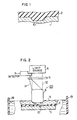
- a pattern 10 formed on a substrate 1 and to be detected for aligning the substrate 1 is covered with a photoresist layer 2 with an uneven surface. Therefore, refraction of light for pattern detection becomes irregular, thus impairing precise position detection.
- the resolution limit R (pm) of a pattern projection optics used for the pattern formation for semiconductor elements is expressed as, where
- the pattern for the formation of the semiconductor element should be finely drawn and the resolution limit R of the pattern projection optics should be improved.
- a pattern forming apparatus 20 using such an optically transparent liquid has a fundamental construction as shown in Fig. 2.
- the apparatus 20 comprises an illumination system 6 comprised of a lamp housing unit and condenser lenses (not shown), a reticle 5 provided with a pattern, reduction lenses 4, a semiconductor substrate 1 carried on a wafer stage (not shown) and having a surface on which a photoresist layer 2 is formed, a liquid layer 3 filling a gap between the photoresist layer 2 and at least a portion of the reduction lenses 4, and a pattern detector 7 for positioning the reticle 5 and the substrate 1.
- an illumination system 6 comprised of a lamp housing unit and condenser lenses (not shown), a reticle 5 provided with a pattern, reduction lenses 4, a semiconductor substrate 1 carried on a wafer stage (not shown) and having a surface on which a photoresist layer 2 is formed, a liquid layer 3 filling a gap between the photoresist layer 2 and at least a portion of the reduction lenses 4, and a
- a positioning pattern formed on the reticle 5 and a positioning pattern 10 formed on the substrate 1 are first brought into alignment by means of the pattern detector 7 through the reduction lenses 4.
- An optical path 11 in this alignment process is shown by solid lines.
- the reticle 5 provided with a predetermined magnified pattern is illuminated by the illumination system 6 to form an optical pattern image of the magnified pattern.
- This optical pattern image is reduced and projected by the reduction lenses 4 upon the photoresist layer 2 coated on the semiconductor substrate 1 to expose the photoresist layer 2.
- An optical path 12 in this process is, shown by dotted lines.
- the wafer stage carrying the semiconductor substrate 1 is moved (stepped) and a next exposure field is exposed (i.e. exposure is repeated) in the same manner as the first exposure process.
- the pattern forming apparatus 20 of the type described above is usually termed a reduction projection aligner, and its general construction, but without the optically transparent liquid, is referred to as Step & Repeat Camera, for the detail of which reference may be made to US Patent No. 4,057,347.
- the pattern forming apparatus 20, as shown in Fig. 2 has the liquid layer 3 formed and sustained between the reduction lenses 4 and the photoresist layer 2 as has already been described above.
- the semiconductor substrate 1 provided with the photoresist layer 2 and a portion or a whole of the reduction lenses 4 are immersed in the liquid layer 3.
- This liquid layer 3 contains a liquid which can transmit the optical pattern image, that is, optically transparent and has a refractive index of more than 1 (one). Needless to say, the liquid should not be reactive with materials of the reduction lenses 4, photoresist layer 2 and semiconductor substrate 1, i.e. should have chemically stable characteristics. Exemplified as the liquid of this nature are trichlorotrifluoroethane (C 2 CI 3 F 3 ), chlorobenzene (C s H s CI), and water.
- the liquid is filled in a pool 19 and the reduction lenses 4 and the semiconductor substrate 1 are disposed in the pool 19.
- FIG. 3 An embodiment 20' of the invention is shown in Fig. 3.
- a member 9 is provided which surrounds the reduction lenses 4 and forms and sustains the liquid layer 3, and the sustaining member 9 is equipped with a nozzle 13. Liquid supplied to the nozzle 13 in a direction of an arrow 8 is drawn out toward the semiconductor substrate 1. The reduction lenses 4 and the photoresist layer 2 are put in immersion in the liquid layer 3.
- the refractive indices of the photoresist layer 2 formed on the substrate 1 and of the liquid layer 3 are made equal or almost equal, there occurs no or almost no such error in position detection, which is ascribed to the unevenness of the photoresist layer and has occurred in the conventional system upon detection of the pattern 10 by the position detector 7, even with a photoresist layer 2 having an uneven surface as shown in Fig. 3.
- the optical affect of the unevenness of the photoresist layer 2 can be eliminated essentially by melting the optical interface at the photoresist surface in an optically uniform medium, thereby ensuring a stable and highly precise pattern detection.
- the apparatus described above is also advantageous in that since the liquid used in the invention can be kept clean by, for example, distillation. It is expected that failure due to the deposition of dusts contained in air to the surface of the photoresist layer 2, which would occur in the conventional apparatus without a liquid layer, can be prevented. Especially, when forming a fine exposure field of less than 1 11m line width with a reduction projection aligner, difficulties have been encountered in removing fine dusts contained in air which may otherwise be deposited to the fine pattern. But, such difficulties can advantageously be overcome by the use of a liquid layer.
- the substrate 1 can be less affected by temperature variations in the course of exposure and possible alignment error due to in-plane distortion of the substrate can be prevented in advance.
Landscapes
- Physics & Mathematics (AREA)
- General Physics & Mathematics (AREA)
- Exposure Of Semiconductors, Excluding Electron Or Ion Beam Exposure (AREA)
- Exposure And Positioning Against Photoresist Photosensitive Materials (AREA)
Claims (3)
Applications Claiming Priority (2)
| Application Number | Priority Date | Filing Date | Title |
|---|---|---|---|
| JP56037977A JPS57153433A (en) | 1981-03-18 | 1981-03-18 | Manufacturing device for semiconductor |
| JP37977/81 | 1981-03-18 |
Publications (3)
| Publication Number | Publication Date |
|---|---|
| EP0060729A2 EP0060729A2 (de) | 1982-09-22 |
| EP0060729A3 EP0060729A3 (en) | 1983-03-16 |
| EP0060729B1 true EP0060729B1 (de) | 1986-08-13 |
Family
ID=12512621
Family Applications (1)
| Application Number | Title | Priority Date | Filing Date |
|---|---|---|---|
| EP82301377A Expired EP0060729B1 (de) | 1981-03-18 | 1982-03-17 | Anordnung zur Ausbildung von Mustern |
Country Status (5)
| Country | Link |
|---|---|
| US (1) | US4480910A (de) |
| EP (1) | EP0060729B1 (de) |
| JP (1) | JPS57153433A (de) |
| CA (1) | CA1159160A (de) |
| DE (1) | DE3272511D1 (de) |
Cited By (1)
| Publication number | Priority date | Publication date | Assignee | Title |
|---|---|---|---|---|
| US8384874B2 (en) | 2004-07-12 | 2013-02-26 | Nikon Corporation | Immersion exposure apparatus and device manufacturing method to detect if liquid on base member |
Families Citing this family (438)
| Publication number | Priority date | Publication date | Assignee | Title |
|---|---|---|---|---|
| GB8919617D0 (en) * | 1989-08-30 | 1989-10-11 | Crosfield Electronics Ltd | Film transparency holder |
| JP2753930B2 (ja) * | 1992-11-27 | 1998-05-20 | キヤノン株式会社 | 液浸式投影露光装置 |
| JP3221226B2 (ja) * | 1994-03-30 | 2001-10-22 | キヤノン株式会社 | 照明装置及びそれを用いた投影露光装置 |
| WO1999049504A1 (fr) * | 1998-03-26 | 1999-09-30 | Nikon Corporation | Procede et systeme d'exposition par projection |
| US7187503B2 (en) * | 1999-12-29 | 2007-03-06 | Carl Zeiss Smt Ag | Refractive projection objective for immersion lithography |
| KR100866818B1 (ko) * | 2000-12-11 | 2008-11-04 | 가부시키가이샤 니콘 | 투영광학계 및 이 투영광학계를 구비한 노광장치 |
| WO2002091078A1 (en) * | 2001-05-07 | 2002-11-14 | Massachusetts Institute Of Technology | Methods and apparatus employing an index matching medium |
| US7092069B2 (en) * | 2002-03-08 | 2006-08-15 | Carl Zeiss Smt Ag | Projection exposure method and projection exposure system |
| DE10210899A1 (de) * | 2002-03-08 | 2003-09-18 | Zeiss Carl Smt Ag | Refraktives Projektionsobjektiv für Immersions-Lithographie |
| JP2005536775A (ja) * | 2002-08-23 | 2005-12-02 | 株式会社ニコン | 投影光学系、フォトリソグラフィ方法および露光装置、並びに露光装置を用いた方法 |
| US6788477B2 (en) * | 2002-10-22 | 2004-09-07 | Taiwan Semiconductor Manufacturing Co., Ltd. | Apparatus for method for immersion lithography |
| US9482966B2 (en) | 2002-11-12 | 2016-11-01 | Asml Netherlands B.V. | Lithographic apparatus and device manufacturing method |
| KR100585476B1 (ko) * | 2002-11-12 | 2006-06-07 | 에이에스엠엘 네델란즈 비.브이. | 리소그래피 장치 및 디바이스 제조방법 |
| SG121822A1 (en) * | 2002-11-12 | 2006-05-26 | Asml Netherlands Bv | Lithographic apparatus and device manufacturing method |
| DE60335595D1 (de) * | 2002-11-12 | 2011-02-17 | Asml Netherlands Bv | Lithographischer Apparat mit Immersion und Verfahren zur Herstellung einer Vorrichtung |
| SG121819A1 (en) | 2002-11-12 | 2006-05-26 | Asml Netherlands Bv | Lithographic apparatus and device manufacturing method |
| US10503084B2 (en) | 2002-11-12 | 2019-12-10 | Asml Netherlands B.V. | Lithographic apparatus and device manufacturing method |
| CN101382738B (zh) | 2002-11-12 | 2011-01-12 | Asml荷兰有限公司 | 光刻投射装置 |
| EP1429188B1 (de) * | 2002-11-12 | 2013-06-19 | ASML Netherlands B.V. | Lithographischer Projektionsapparat |
| US7372541B2 (en) | 2002-11-12 | 2008-05-13 | Asml Netherlands B.V. | Lithographic apparatus and device manufacturing method |
| EP1420298B1 (de) * | 2002-11-12 | 2013-02-20 | ASML Netherlands B.V. | Lithographischer Apparat |
| US7110081B2 (en) * | 2002-11-12 | 2006-09-19 | Asml Netherlands B.V. | Lithographic apparatus and device manufacturing method |
| SG131766A1 (en) * | 2002-11-18 | 2007-05-28 | Asml Netherlands Bv | Lithographic apparatus and device manufacturing method |
| DE10253679A1 (de) * | 2002-11-18 | 2004-06-03 | Infineon Technologies Ag | Optische Einrichtung zur Verwendung bei einem Lithographie-Verfahren, insbesondere zur Herstellung eines Halbleiter-Bauelements, sowie optisches Lithographieverfahren |
| TWI255971B (en) * | 2002-11-29 | 2006-06-01 | Asml Netherlands Bv | Lithographic apparatus and device manufacturing method |
| DE10258718A1 (de) * | 2002-12-09 | 2004-06-24 | Carl Zeiss Smt Ag | Projektionsobjektiv, insbesondere für die Mikrolithographie, sowie Verfahren zur Abstimmung eines Projektionsobjektives |
| JP4352874B2 (ja) | 2002-12-10 | 2009-10-28 | 株式会社ニコン | 露光装置及びデバイス製造方法 |
| EP1571700A4 (de) | 2002-12-10 | 2007-09-12 | Nikon Corp | Optische vorrichtung und projektionsbelichtungsvorrichtung unter verwendung der optischen vorrichtung |
| SG171468A1 (en) | 2002-12-10 | 2011-06-29 | Nikon Corp | Exposure apparatus and method for producing device |
| DE10257766A1 (de) * | 2002-12-10 | 2004-07-15 | Carl Zeiss Smt Ag | Verfahren zur Einstellung einer gewünschten optischen Eigenschaft eines Projektionsobjektivs sowie mikrolithografische Projektionsbelichtungsanlage |
| US7948604B2 (en) | 2002-12-10 | 2011-05-24 | Nikon Corporation | Exposure apparatus and method for producing device |
| EP1429190B1 (de) * | 2002-12-10 | 2012-05-09 | Canon Kabushiki Kaisha | Belichtungsapparat und -verfahren |
| CN101872135B (zh) * | 2002-12-10 | 2013-07-31 | 株式会社尼康 | 曝光设备和器件制造法 |
| EP1571695A4 (de) | 2002-12-10 | 2008-10-15 | Nikon Corp | Belichtungsvorrichtung und verfahren zur herstellung der vorrichtung |
| US7242455B2 (en) | 2002-12-10 | 2007-07-10 | Nikon Corporation | Exposure apparatus and method for producing device |
| AU2003289271A1 (en) * | 2002-12-10 | 2004-06-30 | Nikon Corporation | Exposure apparatus, exposure method and method for manufacturing device |
| USRE48515E1 (en) * | 2002-12-19 | 2021-04-13 | Asml Netherlands B.V. | Method and device for irradiating spots on a layer |
| EP1732075A3 (de) * | 2002-12-19 | 2007-02-21 | Koninklijke Philips Electronics N.V. | Verfahren und Vorrichtung zur Punktbestrahlung auf einer Schicht |
| DE10261775A1 (de) * | 2002-12-20 | 2004-07-01 | Carl Zeiss Smt Ag | Vorrichtung zur optischen Vermessung eines Abbildungssystems |
| EP2466621B1 (de) | 2003-02-26 | 2015-04-01 | Nikon Corporation | Belichtungsvorrichtung, Belichtungsverfahren und Verfahren zur Herstellung des Geräts |
| CN101354539B (zh) * | 2003-02-26 | 2011-01-26 | 株式会社尼康 | 曝光装置和器件制造方法 |
| KR101181688B1 (ko) | 2003-03-25 | 2012-09-19 | 가부시키가이샤 니콘 | 노광 장치 및 디바이스 제조 방법 |
| AU2003219097A1 (en) * | 2003-03-26 | 2004-10-18 | Carl Zeiss Smt Ag | Device for the low-deformation replaceable mounting of an optical element |
| JP4902201B2 (ja) | 2003-04-07 | 2012-03-21 | 株式会社ニコン | 露光装置、露光方法及びデバイス製造方法 |
| WO2004093159A2 (en) | 2003-04-09 | 2004-10-28 | Nikon Corporation | Immersion lithography fluid control system |
| KR20170018113A (ko) | 2003-04-09 | 2017-02-15 | 가부시키가이샤 니콘 | 노광 방법 및 장치, 그리고 디바이스 제조 방법 |
| JP4656057B2 (ja) * | 2003-04-10 | 2011-03-23 | 株式会社ニコン | 液浸リソグラフィ装置用電気浸透素子 |
| EP2921905B1 (de) | 2003-04-10 | 2017-12-27 | Nikon Corporation | Ablaufweg zum sammeln von flüssigkeiten für eine immersionslithografievorrichtung |
| KR101177330B1 (ko) | 2003-04-10 | 2012-08-30 | 가부시키가이샤 니콘 | 액침 리소그래피 장치 |
| WO2004090634A2 (en) * | 2003-04-10 | 2004-10-21 | Nikon Corporation | Environmental system including vaccum scavange for an immersion lithography apparatus |
| WO2004092830A2 (en) | 2003-04-11 | 2004-10-28 | Nikon Corporation | Liquid jet and recovery system for immersion lithography |
| KR101159564B1 (ko) | 2003-04-11 | 2012-06-25 | 가부시키가이샤 니콘 | 액침 리소그래피 머신에서 웨이퍼 교환동안 투영 렌즈 아래의 갭에서 액침액체를 유지하는 장치 및 방법 |
| KR20170016014A (ko) | 2003-04-11 | 2017-02-10 | 가부시키가이샤 니콘 | 액침 리소그래피에 의한 광학기기의 세정방법 |
| ATE542167T1 (de) | 2003-04-17 | 2012-02-15 | Nikon Corp | Lithographisches immersionsgerät |
| US7348575B2 (en) | 2003-05-06 | 2008-03-25 | Nikon Corporation | Projection optical system, exposure apparatus, and exposure method |
| SG10201405231YA (en) | 2003-05-06 | 2014-09-26 | Nippon Kogaku Kk | Projection optical system, exposure apparatus, and exposure method |
| JP4025683B2 (ja) * | 2003-05-09 | 2007-12-26 | 松下電器産業株式会社 | パターン形成方法及び露光装置 |
| TWI295414B (en) | 2003-05-13 | 2008-04-01 | Asml Netherlands Bv | Lithographic apparatus and device manufacturing method |
| CN100437358C (zh) | 2003-05-15 | 2008-11-26 | 株式会社尼康 | 曝光装置及器件制造方法 |
| TWI424470B (zh) | 2003-05-23 | 2014-01-21 | 尼康股份有限公司 | A method of manufacturing an exposure apparatus and an element |
| TWI421911B (zh) | 2003-05-23 | 2014-01-01 | 尼康股份有限公司 | An exposure method, an exposure apparatus, and an element manufacturing method |
| CN100541717C (zh) | 2003-05-28 | 2009-09-16 | 株式会社尼康 | 曝光方法、曝光装置以及器件制造方法 |
| TWI347741B (en) * | 2003-05-30 | 2011-08-21 | Asml Netherlands Bv | Lithographic apparatus and device manufacturing method |
| EP1482372B1 (de) | 2003-05-30 | 2014-10-08 | ASML Netherlands B.V. | Lithographischer Apparat und Verfahren zur Herstellung einer Vorrichtung |
| US7213963B2 (en) | 2003-06-09 | 2007-05-08 | Asml Netherlands B.V. | Lithographic apparatus and device manufacturing method |
| EP2261742A3 (de) * | 2003-06-11 | 2011-05-25 | ASML Netherlands BV | Lithographischer Apparat und Verfahren zur Herstellung einer Vorrichtung |
| US7317504B2 (en) | 2004-04-08 | 2008-01-08 | Asml Netherlands B.V. | Lithographic apparatus and device manufacturing method |
| KR101520591B1 (ko) | 2003-06-13 | 2015-05-14 | 가부시키가이샤 니콘 | 노광 방법, 기판 스테이지, 노광 장치, 및 디바이스 제조 방법 |
| TWI515770B (zh) | 2003-06-19 | 2016-01-01 | 尼康股份有限公司 | An exposure apparatus, an exposure method, and an element manufacturing method |
| US6867844B2 (en) * | 2003-06-19 | 2005-03-15 | Asml Holding N.V. | Immersion photolithography system and method using microchannel nozzles |
| JP2005019616A (ja) | 2003-06-25 | 2005-01-20 | Canon Inc | 液浸式露光装置 |
| EP1498778A1 (de) * | 2003-06-27 | 2005-01-19 | ASML Netherlands B.V. | Lithographischer Apparat und Verfahren zur Herstellung einer Vorrichtung |
| EP1491956B1 (de) * | 2003-06-27 | 2006-09-06 | ASML Netherlands B.V. | Lithographischer Apparat und Verfahren zur Herstellung eines Artikels |
| US6809794B1 (en) * | 2003-06-27 | 2004-10-26 | Asml Holding N.V. | Immersion photolithography system and method using inverted wafer-projection optics interface |
| EP1494074A1 (de) * | 2003-06-30 | 2005-01-05 | ASML Netherlands B.V. | Lithographischer Apparat und Verfahren zur Herstellung einer Vorrichtung |
| EP1975721A1 (de) * | 2003-06-30 | 2008-10-01 | ASML Netherlands B.V. | Lithographischer Apparat und Verfahren zur Herstellung eines Artikels |
| WO2005006026A2 (en) * | 2003-07-01 | 2005-01-20 | Nikon Corporation | Using isotopically specified fluids as optical elements |
| EP2466382B1 (de) * | 2003-07-08 | 2014-11-26 | Nikon Corporation | Wafertisch für die Immersionslithografie |
| WO2005006418A1 (ja) | 2003-07-09 | 2005-01-20 | Nikon Corporation | 露光装置及びデバイス製造方法 |
| ATE513309T1 (de) * | 2003-07-09 | 2011-07-15 | Nikon Corp | Belichtungsvorrichtung und verfahren zur bauelementeherstellung |
| WO2005006416A1 (ja) * | 2003-07-09 | 2005-01-20 | Nikon Corporation | 結合装置、露光装置、及びデバイス製造方法 |
| EP1646074A4 (de) * | 2003-07-09 | 2007-10-03 | Nikon Corp | Belichtungsvorrichtung und verfahren zur bauelementeherstellung |
| SG109000A1 (en) * | 2003-07-16 | 2005-02-28 | Asml Netherlands Bv | Lithographic apparatus and device manufacturing method |
| EP1500982A1 (de) | 2003-07-24 | 2005-01-26 | ASML Netherlands B.V. | Lithographischer Apparat und Verfahren zur Herstellung eines Artikels |
| US7006209B2 (en) * | 2003-07-25 | 2006-02-28 | Advanced Micro Devices, Inc. | Method and apparatus for monitoring and controlling imaging in immersion lithography systems |
| EP1650787A4 (de) * | 2003-07-25 | 2007-09-19 | Nikon Corp | Untersuchungsverfahren und untersuchungseinrichtung für ein optisches projektionssystem und herstellungsverfahren für ein optisches projektionssystem |
| CN102043350B (zh) * | 2003-07-28 | 2014-01-29 | 株式会社尼康 | 曝光装置、器件制造方法、及曝光装置的控制方法 |
| US7175968B2 (en) * | 2003-07-28 | 2007-02-13 | Asml Netherlands B.V. | Lithographic apparatus, device manufacturing method and a substrate |
| US7326522B2 (en) | 2004-02-11 | 2008-02-05 | Asml Netherlands B.V. | Device manufacturing method and a substrate |
| EP1503244A1 (de) | 2003-07-28 | 2005-02-02 | ASML Netherlands B.V. | Lithographischer Projektionsapparat und Verfahren zur Herstellung einer Vorrichtung |
| US7779781B2 (en) | 2003-07-31 | 2010-08-24 | Asml Netherlands B.V. | Lithographic apparatus and device manufacturing method |
| US7061578B2 (en) * | 2003-08-11 | 2006-06-13 | Advanced Micro Devices, Inc. | Method and apparatus for monitoring and controlling imaging in immersion lithography systems |
| SG109614A1 (en) * | 2003-08-11 | 2005-03-30 | Taiwan Semiconductor Mfg | Lithography apparatus for manufacture of integrated circuits |
| US7700267B2 (en) * | 2003-08-11 | 2010-04-20 | Taiwan Semiconductor Manufacturing Company, Ltd. | Immersion fluid for immersion lithography, and method of performing immersion lithography |
| US7579135B2 (en) * | 2003-08-11 | 2009-08-25 | Taiwan Semiconductor Manufacturing Company, Ltd. | Lithography apparatus for manufacture of integrated circuits |
| KR101381563B1 (ko) * | 2003-08-21 | 2014-04-04 | 가부시키가이샤 니콘 | 노광 장치, 노광 방법 및 디바이스 제조 방법 |
| US8149381B2 (en) * | 2003-08-26 | 2012-04-03 | Nikon Corporation | Optical element and exposure apparatus |
| EP2278402B1 (de) | 2003-08-26 | 2013-03-06 | Nikon Corporation | Belichtungsvorrichtung |
| TWI263859B (en) | 2003-08-29 | 2006-10-11 | Asml Netherlands Bv | Lithographic apparatus and device manufacturing method |
| CN100407371C (zh) | 2003-08-29 | 2008-07-30 | 株式会社尼康 | 曝光装置和器件加工方法 |
| US6954256B2 (en) | 2003-08-29 | 2005-10-11 | Asml Netherlands B.V. | Gradient immersion lithography |
| TWI245163B (en) * | 2003-08-29 | 2005-12-11 | Asml Netherlands Bv | Lithographic apparatus and device manufacturing method |
| EP2261740B1 (de) | 2003-08-29 | 2014-07-09 | ASML Netherlands BV | Lithographischer Apparat |
| US7014966B2 (en) * | 2003-09-02 | 2006-03-21 | Advanced Micro Devices, Inc. | Method and apparatus for elimination of bubbles in immersion medium in immersion lithography systems |
| KR101523180B1 (ko) | 2003-09-03 | 2015-05-26 | 가부시키가이샤 니콘 | 액침 리소그래피용 유체를 제공하기 위한 장치 및 방법 |
| KR101162527B1 (ko) * | 2003-09-03 | 2012-07-09 | 가부시키가이샤 니콘 | 노광 장치 및 디바이스 제조 방법 |
| US7166418B2 (en) | 2003-09-03 | 2007-01-23 | Matsushita Electric Industrial Co., Ltd. | Sulfonamide compound, polymer compound, resist material and pattern formation method |
| WO2005029559A1 (ja) * | 2003-09-19 | 2005-03-31 | Nikon Corporation | 露光装置及びデバイス製造方法 |
| KR101248325B1 (ko) * | 2003-09-26 | 2013-03-27 | 가부시키가이샤 니콘 | 투영노광장치 및 투영노광장치의 세정방법, 메인터넌스방법 그리고 디바이스의 제조방법 |
| CN1860585B (zh) * | 2003-09-29 | 2010-04-28 | 株式会社尼康 | 液浸型透镜系统和投影曝光装置 |
| EP1519230A1 (de) * | 2003-09-29 | 2005-03-30 | ASML Netherlands B.V. | Lithographischer Apparat und Methode zur Herstellung einer Vorrichtung |
| WO2005031824A1 (ja) * | 2003-09-29 | 2005-04-07 | Nikon Corporation | 投影露光装置、投影露光方法およびデバイス製造方法 |
| DE60302897T2 (de) * | 2003-09-29 | 2006-08-03 | Asml Netherlands B.V. | Lithographischer Apparat und Verfahren zur Herstellung einer Vorrichtung |
| KR101664642B1 (ko) | 2003-09-29 | 2016-10-11 | 가부시키가이샤 니콘 | 노광장치, 노광방법 및 디바이스 제조방법 |
| US7158211B2 (en) * | 2003-09-29 | 2007-01-02 | Asml Netherlands B.V. | Lithographic apparatus and device manufacturing method |
| US7056646B1 (en) * | 2003-10-01 | 2006-06-06 | Advanced Micro Devices, Inc. | Use of base developers as immersion lithography fluid |
| US7169530B2 (en) | 2003-10-02 | 2007-01-30 | Matsushita Electric Industrial Co., Ltd. | Polymer compound, resist material and pattern formation method |
| ITMI20031914A1 (it) * | 2003-10-03 | 2005-04-04 | Solvay Solexis Spa | Perfluoropolieteri. |
| US7369217B2 (en) * | 2003-10-03 | 2008-05-06 | Micronic Laser Systems Ab | Method and device for immersion lithography |
| EP1672682A4 (de) | 2003-10-08 | 2008-10-15 | Zao Nikon Co Ltd | Substrat-transport-vorrichtung und -verfahren, belichtungs-vorrichtung und -verfahren und bauelementherstellungsverfahren |
| JP2005136364A (ja) * | 2003-10-08 | 2005-05-26 | Zao Nikon Co Ltd | 基板搬送装置、露光装置、並びにデバイス製造方法 |
| WO2005036621A1 (ja) | 2003-10-08 | 2005-04-21 | Zao Nikon Co., Ltd. | 基板搬送装置及び基板搬送方法、露光装置及び露光方法、デバイス製造方法 |
| TWI598934B (zh) | 2003-10-09 | 2017-09-11 | 尼康股份有限公司 | Exposure apparatus, exposure method, and device manufacturing method |
| EP1524557A1 (de) * | 2003-10-15 | 2005-04-20 | ASML Netherlands B.V. | Lithographischer Apparat und Methode zur Herstellung einer Vorrichtung |
| EP1524558A1 (de) | 2003-10-15 | 2005-04-20 | ASML Netherlands B.V. | Lithographischer Apparat und Verfahren zur Herstellung einer Vorrichtung |
| WO2005050321A1 (de) | 2003-10-22 | 2005-06-02 | Carl Zeiss Smt Ag | Refraktives projektionsobjektiv für die immersions-lithographie |
| US7411653B2 (en) * | 2003-10-28 | 2008-08-12 | Asml Netherlands B.V. | Lithographic apparatus |
| US7352433B2 (en) | 2003-10-28 | 2008-04-01 | Asml Netherlands B.V. | Lithographic apparatus and device manufacturing method |
| EP1679738A4 (de) * | 2003-10-28 | 2008-08-06 | Nikon Corp | Belichtungsvorrichtung, belichtungsverfahren und bauelementeherstellungsverfahren |
| TW201834020A (zh) | 2003-10-28 | 2018-09-16 | 日商尼康股份有限公司 | 照明光學裝置、曝光裝置、曝光方法以及元件製造方法 |
| US7113259B2 (en) * | 2003-10-31 | 2006-09-26 | Asml Netherlands B.V. | Lithographic apparatus and device manufacturing method |
| CN100461336C (zh) | 2003-10-31 | 2009-02-11 | 株式会社尼康 | 曝光装置以及器件制造方法 |
| EP1531362A3 (de) * | 2003-11-13 | 2007-07-25 | Matsushita Electric Industrial Co., Ltd. | Vorrichtung zur Herstellung von Halbleitern und Methode zur Bildung von Mustern |
| US7528929B2 (en) | 2003-11-14 | 2009-05-05 | Asml Netherlands B.V. | Lithographic apparatus and device manufacturing method |
| TW201809801A (zh) | 2003-11-20 | 2018-03-16 | 日商尼康股份有限公司 | 光學照明裝置、曝光裝置、曝光方法、以及元件製造方法 |
| US7545481B2 (en) * | 2003-11-24 | 2009-06-09 | Asml Netherlands B.V. | Lithographic apparatus and device manufacturing method |
| EP2717295B1 (de) | 2003-12-03 | 2018-07-18 | Nikon Corporation | Belichtungsvorrichtung, Belichtungsverfahren, und Verfahren zur Herstellung einer Vorrichtung |
| JP2005175034A (ja) * | 2003-12-09 | 2005-06-30 | Canon Inc | 露光装置 |
| DE602004030481D1 (de) | 2003-12-15 | 2011-01-20 | Nippon Kogaku Kk | Bühnensystem, belichtungsvorrichtung und belichtungsverfahren |
| KR101111363B1 (ko) * | 2003-12-15 | 2012-04-12 | 가부시키가이샤 니콘 | 투영노광장치 및 스테이지 장치, 그리고 노광방법 |
| JP2005183438A (ja) * | 2003-12-16 | 2005-07-07 | Matsushita Electric Ind Co Ltd | パターン形成方法 |
| US7460206B2 (en) * | 2003-12-19 | 2008-12-02 | Carl Zeiss Smt Ag | Projection objective for immersion lithography |
| US7589818B2 (en) * | 2003-12-23 | 2009-09-15 | Asml Netherlands B.V. | Lithographic apparatus, alignment apparatus, device manufacturing method, and a method of converting an apparatus |
| US7394521B2 (en) | 2003-12-23 | 2008-07-01 | Asml Netherlands B.V. | Lithographic apparatus and device manufacturing method |
| EP3376523A1 (de) * | 2004-01-05 | 2018-09-19 | Nikon Corporation | Belichtungsvorrichtung, belichtungsverfahren und verfahren zur herstellung einer vorrichtung |
| JP4253592B2 (ja) * | 2004-01-06 | 2009-04-15 | オリンパス株式会社 | 液浸対物レンズ、蛍光分析装置および倒立型顕微鏡。 |
| CN1938646B (zh) | 2004-01-20 | 2010-12-15 | 卡尔蔡司Smt股份公司 | 曝光装置和用于投影透镜的测量装置 |
| TWI259319B (en) | 2004-01-23 | 2006-08-01 | Air Prod & Chem | Immersion lithography fluids |
| US20050161644A1 (en) * | 2004-01-23 | 2005-07-28 | Peng Zhang | Immersion lithography fluids |
| US7697110B2 (en) * | 2004-01-26 | 2010-04-13 | Nikon Corporation | Exposure apparatus and device manufacturing method |
| US7589822B2 (en) | 2004-02-02 | 2009-09-15 | Nikon Corporation | Stage drive method and stage unit, exposure apparatus, and device manufacturing method |
| JP2007520893A (ja) * | 2004-02-03 | 2007-07-26 | ロチェスター インスティテュート オブ テクノロジー | 流体を使用したフォトリソグラフィ法及びそのシステム |
| EP1713114B1 (de) | 2004-02-03 | 2018-09-19 | Nikon Corporation | Belichtungsvorrichtung und verfahren zur herstellung einer vorrichtung |
| TW200537255A (en) * | 2004-02-04 | 2005-11-16 | Nikon Corp | Exposure equipment and method, position control method and device manufacturing method |
| EP1713115B1 (de) | 2004-02-04 | 2016-05-04 | Nikon Corporation | Belichtungsvorrichtung, belichtungsverfahren und bauelementeherstellungsverfahren |
| TWI389174B (zh) | 2004-02-06 | 2013-03-11 | 尼康股份有限公司 | 偏光變換元件、光學照明裝置、曝光裝置以及曝光方法 |
| US7050146B2 (en) | 2004-02-09 | 2006-05-23 | Asml Netherlands B.V. | Lithographic apparatus and device manufacturing method |
| JP4529141B2 (ja) * | 2004-02-09 | 2010-08-25 | 好彦 岡本 | 露光装置及びそれを用いた半導体装置の製造方法 |
| JP4018647B2 (ja) * | 2004-02-09 | 2007-12-05 | キヤノン株式会社 | 投影露光装置およびデバイス製造方法 |
| US20070030467A1 (en) * | 2004-02-19 | 2007-02-08 | Nikon Corporation | Exposure apparatus, exposure method, and device fabricating method |
| WO2005081291A1 (ja) * | 2004-02-19 | 2005-09-01 | Nikon Corporation | 露光装置及びデバイスの製造方法 |
| KR101106497B1 (ko) * | 2004-02-20 | 2012-01-20 | 가부시키가이샤 니콘 | 노광 장치, 공급 방법 및 회수 방법, 노광 방법, 및디바이스 제조 방법 |
| TWI371657B (en) | 2004-02-20 | 2012-09-01 | Fujifilm Corp | Positive resist composition for immersion exposure and method of pattern formation with the same |
| JP4365236B2 (ja) | 2004-02-20 | 2009-11-18 | 富士フイルム株式会社 | 液浸露光用レジスト組成物及びそれを用いたパターン形成方法 |
| WO2005081295A1 (ja) * | 2004-02-20 | 2005-09-01 | Nikon Corporation | 露光方法、露光装置及び露光システム並びにデバイス製造方法 |
| WO2005081063A1 (ja) * | 2004-02-20 | 2005-09-01 | Daikin Industries, Ltd. | 液浸リソグラフィーに用いるレジスト積層体 |
| US8488102B2 (en) * | 2004-03-18 | 2013-07-16 | Taiwan Semiconductor Manufacturing Company, Ltd. | Immersion fluid for immersion lithography, and method of performing immersion lithography |
| US7906268B2 (en) | 2004-03-18 | 2011-03-15 | Fujifilm Corporation | Positive resist composition for immersion exposure and pattern-forming method using the same |
| KR101851511B1 (ko) | 2004-03-25 | 2018-04-23 | 가부시키가이샤 니콘 | 노광 장치 및 디바이스 제조 방법 |
| EP1737024A4 (de) * | 2004-03-25 | 2008-10-15 | Nikon Corp | Belichtungsgeräte, belichtungsverfahren und bauelemente-herstellungsverfahren |
| TW200605191A (en) * | 2004-03-30 | 2006-02-01 | Nikon Corp | Exposure apparatus, exposure method, device manufacturing method, and surface shape detecting device |
| US7227619B2 (en) * | 2004-04-01 | 2007-06-05 | Asml Netherlands B.V. | Lithographic apparatus and device manufacturing method |
| US7034917B2 (en) * | 2004-04-01 | 2006-04-25 | Asml Netherlands B.V. | Lithographic apparatus, device manufacturing method and device manufactured thereby |
| US7295283B2 (en) * | 2004-04-02 | 2007-11-13 | Asml Netherlands B.V. | Lithographic apparatus and device manufacturing method |
| US7898642B2 (en) | 2004-04-14 | 2011-03-01 | Asml Netherlands B.V. | Lithographic apparatus and device manufacturing method |
| EP1753016B1 (de) | 2004-04-19 | 2012-06-20 | Nikon Corporation | Belichtungsvorrichtung und bauelemente-herstellungsverfahren |
| US7379159B2 (en) | 2004-05-03 | 2008-05-27 | Asml Netherlands B.V. | Lithographic apparatus and device manufacturing method |
| EP1747499A2 (de) | 2004-05-04 | 2007-01-31 | Nikon Corporation | Vorrichtung und verfahren zur bereitstellung eines fluids für die immersionslithographie |
| US7091502B2 (en) * | 2004-05-12 | 2006-08-15 | Taiwan Semiconductor Manufacturing, Co., Ltd. | Apparatus and method for immersion lithography |
| ATE450813T1 (de) | 2004-05-17 | 2009-12-15 | Fujifilm Corp | Verfahren zur erzeugung eines musters |
| US7616383B2 (en) | 2004-05-18 | 2009-11-10 | Asml Netherlands B.V. | Lithographic apparatus and device manufacturing method |
| US7486381B2 (en) * | 2004-05-21 | 2009-02-03 | Asml Netherlands B.V. | Lithographic apparatus and device manufacturing method |
| CN1954408B (zh) * | 2004-06-04 | 2012-07-04 | 尼康股份有限公司 | 曝光装置、曝光方法及元件制造方法 |
| EP1774405B1 (de) | 2004-06-04 | 2014-08-06 | Carl Zeiss SMT GmbH | System zur messung der bildqualität eines optischen bildgebungssystems |
| US20070103661A1 (en) * | 2004-06-04 | 2007-05-10 | Nikon Corporation | Exposure apparatus, exposure method, and method for producing device |
| WO2005122242A1 (ja) * | 2004-06-07 | 2005-12-22 | Nikon Corporation | ステージ装置、露光装置及び露光方法 |
| SG186621A1 (en) * | 2004-06-09 | 2013-01-30 | Nikon Corp | Substrate holding device, exposure apparatus having same, exposure method, method for producing device, and liquid repellent plate |
| WO2005122218A1 (ja) * | 2004-06-09 | 2005-12-22 | Nikon Corporation | 露光装置及びデバイス製造方法 |
| US8508713B2 (en) * | 2004-06-10 | 2013-08-13 | Nikon Corporation | Exposure apparatus, exposure method, and method for producing device |
| KR20070026603A (ko) * | 2004-06-10 | 2007-03-08 | 가부시키가이샤 니콘 | 노광 장치, 노광 방법, 및 디바이스 제조 방법 |
| US8373843B2 (en) * | 2004-06-10 | 2013-02-12 | Nikon Corporation | Exposure apparatus, exposure method, and method for producing device |
| US8717533B2 (en) | 2004-06-10 | 2014-05-06 | Nikon Corporation | Exposure apparatus, exposure method, and method for producing device |
| US20070222959A1 (en) * | 2004-06-10 | 2007-09-27 | Nikon Corporation | Exposure apparatus, exposure method, and method for producing device |
| KR20180072867A (ko) | 2004-06-10 | 2018-06-29 | 가부시키가이샤 니콘 | 노광 장치, 노광 방법 및 디바이스 제조 방법 |
| US20070139628A1 (en) * | 2004-06-10 | 2007-06-21 | Nikon Corporation | Exposure apparatus, exposure method, and method for producing device |
| JP4543767B2 (ja) * | 2004-06-10 | 2010-09-15 | 株式会社ニコン | 露光装置及びデバイス製造方法 |
| JP4551701B2 (ja) | 2004-06-14 | 2010-09-29 | 富士フイルム株式会社 | 液浸露光用保護膜形成組成物及びそれを用いたパターン形成方法 |
| US7481867B2 (en) | 2004-06-16 | 2009-01-27 | Edwards Limited | Vacuum system for immersion photolithography |
| EP3098835B1 (de) * | 2004-06-21 | 2017-07-26 | Nikon Corporation | Belichtungsvorrichtung, belichtungsverfahren und vorrichtungsherstellungsverfahren |
| US8698998B2 (en) * | 2004-06-21 | 2014-04-15 | Nikon Corporation | Exposure apparatus, method for cleaning member thereof, maintenance method for exposure apparatus, maintenance device, and method for producing device |
| US8368870B2 (en) * | 2004-06-21 | 2013-02-05 | Nikon Corporation | Exposure apparatus and device manufacturing method |
| CN100547488C (zh) * | 2004-06-23 | 2009-10-07 | 台湾积体电路制造股份有限公司 | 浸入式光学投影系统与集成电路晶片的制造方法 |
| US7057702B2 (en) * | 2004-06-23 | 2006-06-06 | Asml Netherlands B.V. | Lithographic apparatus and device manufacturing method |
| US7463330B2 (en) | 2004-07-07 | 2008-12-09 | Asml Netherlands B.V. | Lithographic apparatus and device manufacturing method |
| TWI368825B (en) | 2004-07-07 | 2012-07-21 | Fujifilm Corp | Positive type resist composition for use in liquid immersion exposure and a method of forming the pattern using the same |
| JP4551704B2 (ja) | 2004-07-08 | 2010-09-29 | 富士フイルム株式会社 | 液浸露光用保護膜形成組成物及びそれを用いたパターン形成方法 |
| DE102004033195A1 (de) * | 2004-07-09 | 2006-02-23 | Leica Microsystems Semiconductor Gmbh | Vorrichtung zur Inspektion eines mikroskopischen Bauteils |
| CN100533661C (zh) * | 2004-07-12 | 2009-08-26 | 株式会社尼康 | 曝光条件的决定方法、曝光方法及装置、组件制造方法 |
| EP1801852A4 (de) * | 2004-07-16 | 2008-04-09 | Nikon Corp | Trägerverfahren und trägerstruktur für optische elemente, optische vorrichtung, belichtungsvorrichtung und herstellungsverfahren für vorrichtung |
| US7161663B2 (en) * | 2004-07-22 | 2007-01-09 | Asml Netherlands B.V. | Lithographic apparatus |
| CN102998910A (zh) * | 2004-08-03 | 2013-03-27 | 株式会社尼康 | 曝光装置的控制方法、曝光方法及组件制造方法 |
| TW200615716A (en) * | 2004-08-05 | 2006-05-16 | Nikon Corp | Stage device and exposure device |
| JP4621451B2 (ja) | 2004-08-11 | 2011-01-26 | 富士フイルム株式会社 | 液浸露光用保護膜形成組成物及びそれを用いたパターン形成方法 |
| US7304715B2 (en) | 2004-08-13 | 2007-12-04 | Asml Netherlands B.V. | Lithographic apparatus and device manufacturing method |
| KR20070048164A (ko) * | 2004-08-18 | 2007-05-08 | 가부시키가이샤 니콘 | 노광 장치 및 디바이스 제조 방법 |
| US7701550B2 (en) | 2004-08-19 | 2010-04-20 | Asml Netherlands B.V. | Lithographic apparatus and device manufacturing method |
| US20060044533A1 (en) * | 2004-08-27 | 2006-03-02 | Asmlholding N.V. | System and method for reducing disturbances caused by movement in an immersion lithography system |
| US20080318152A1 (en) * | 2004-09-17 | 2008-12-25 | Takeyuki Mizutani | Substrate for Exposure, Exposure Method and Device Manufacturing Method |
| US8102512B2 (en) * | 2004-09-17 | 2012-01-24 | Nikon Corporation | Substrate holding device, exposure apparatus, and device manufacturing method |
| KR101700547B1 (ko) * | 2004-09-17 | 2017-01-26 | 가부시키가이샤 니콘 | 노광 장치, 노광 방법 및 디바이스 제조 방법 |
| US7133114B2 (en) * | 2004-09-20 | 2006-11-07 | Asml Netherlands B.V. | Lithographic apparatus and device manufacturing method |
| US20060060653A1 (en) * | 2004-09-23 | 2006-03-23 | Carl Wittenberg | Scanner system and method for simultaneously acquiring data images from multiple object planes |
| US7522261B2 (en) * | 2004-09-24 | 2009-04-21 | Asml Netherlands B.V. | Lithographic apparatus and device manufacturing method |
| US7355674B2 (en) * | 2004-09-28 | 2008-04-08 | Asml Netherlands B.V. | Lithographic apparatus, device manufacturing method and computer program product |
| US7894040B2 (en) | 2004-10-05 | 2011-02-22 | Asml Netherlands B.V. | Lithographic apparatus and device manufacturing method |
| US7209213B2 (en) * | 2004-10-07 | 2007-04-24 | Asml Netherlands B.V. | Lithographic apparatus and device manufacturing method |
| JP4448767B2 (ja) | 2004-10-08 | 2010-04-14 | 富士フイルム株式会社 | ポジ型レジスト組成物及びそれを用いたパターン形成方法 |
| EP1806771A4 (de) * | 2004-10-08 | 2008-06-18 | Nikon Corp | Belichtungseinrichtung und bauelementeherstellungsverfahren |
| KR20070068340A (ko) * | 2004-10-13 | 2007-06-29 | 가부시키가이샤 니콘 | 노광 장치, 노광 방법 및 디바이스 제조 방법 |
| US7852456B2 (en) * | 2004-10-13 | 2010-12-14 | Nikon Corporation | Exposure apparatus, exposure method, and method for producing device |
| EP2426700B1 (de) * | 2004-10-15 | 2018-01-10 | Nikon Corporation | Belichtungsvorrichtung und bauelementeherstellungsverfahren |
| US7379155B2 (en) | 2004-10-18 | 2008-05-27 | Asml Netherlands B.V. | Lithographic apparatus and device manufacturing method |
| US7119876B2 (en) * | 2004-10-18 | 2006-10-10 | Asml Netherlands B.V. | Lithographic apparatus and device manufacturing method |
| US20070242248A1 (en) * | 2004-10-26 | 2007-10-18 | Nikon Corporation | Substrate processing method, exposure apparatus, and method for producing device |
| TWI436403B (zh) * | 2004-10-26 | 2014-05-01 | 尼康股份有限公司 | A cleaning method, a substrate processing method, an exposure apparatus, and an element manufacturing method |
| WO2006049134A1 (ja) | 2004-11-01 | 2006-05-11 | Nikon Corporation | 露光装置及びデバイス製造方法 |
| EP1816671A4 (de) | 2004-11-11 | 2010-01-13 | Nikon Corp | Belichtungsverfahren, bauelementeherstellungsverfahren und substrat |
| US7414699B2 (en) * | 2004-11-12 | 2008-08-19 | Asml Netherlands B.V. | Lithographic apparatus and device manufacturing method |
| US7423720B2 (en) | 2004-11-12 | 2008-09-09 | Asml Netherlands B.V. | Lithographic apparatus and device manufacturing method |
| US7583357B2 (en) * | 2004-11-12 | 2009-09-01 | Asml Netherlands B.V. | Lithographic apparatus and device manufacturing method |
| US7251013B2 (en) | 2004-11-12 | 2007-07-31 | Asml Netherlands B.V. | Lithographic apparatus and device manufacturing method |
| US7411657B2 (en) * | 2004-11-17 | 2008-08-12 | Asml Netherlands B.V. | Lithographic apparatus and device manufacturing method |
| TWI654661B (zh) | 2004-11-18 | 2019-03-21 | Nikon Corporation | 位置測量方法、位置控制方法、測量方法、裝載方法、曝光方法及曝光裝置、及元件製造方法 |
| EP1814146A4 (de) * | 2004-11-19 | 2009-02-11 | Nikon Corp | Aufrechterhaltungsverfahren, belichtungsverfahren, belichtungsvorrichtung und bauelemente-herstellungsverfahren |
| US7119035B2 (en) * | 2004-11-22 | 2006-10-10 | Taiwan Semiconductor Manufacturing Company, Ltd. | Method using specific contact angle for immersion lithography |
| US7732123B2 (en) * | 2004-11-23 | 2010-06-08 | Taiwan Semiconductor Manufacturing Company, Ltd. | Immersion photolithography with megasonic rinse |
| US7145630B2 (en) * | 2004-11-23 | 2006-12-05 | Asml Netherlands B.V. | Lithographic apparatus and device manufacturing method |
| KR101280166B1 (ko) * | 2004-11-25 | 2013-06-28 | 가부시키가이샤 니콘 | 이동체 시스템, 노광 장치 및 디바이스 제조 방법 |
| US7161654B2 (en) * | 2004-12-02 | 2007-01-09 | Asml Netherlands B.V. | Lithographic apparatus and device manufacturing method |
| KR20070083492A (ko) * | 2004-12-02 | 2007-08-24 | 가부시키가이샤 니콘 | 노광 장치, 노광 방법 및 디바이스 제조 방법 |
| US7256121B2 (en) * | 2004-12-02 | 2007-08-14 | Texas Instruments Incorporated | Contact resistance reduction by new barrier stack process |
| US20080106718A1 (en) * | 2004-12-02 | 2008-05-08 | Nikon Corporation | Exposure Apparatus and Device Manufacturing Method |
| US7446850B2 (en) * | 2004-12-03 | 2008-11-04 | Asml Netherlands B.V. | Lithographic apparatus and device manufacturing method |
| WO2006062065A1 (ja) | 2004-12-06 | 2006-06-15 | Nikon Corporation | メンテナンス方法、メンテナンス機器、露光装置、及びデバイス製造方法 |
| TW200625026A (en) * | 2004-12-06 | 2006-07-16 | Nikon Corp | Substrate processing method, method of exposure, exposure device and device manufacturing method |
| US7196770B2 (en) * | 2004-12-07 | 2007-03-27 | Asml Netherlands B.V. | Prewetting of substrate before immersion exposure |
| US7248334B2 (en) * | 2004-12-07 | 2007-07-24 | Asml Netherlands B.V. | Sensor shield |
| US7397533B2 (en) | 2004-12-07 | 2008-07-08 | Asml Netherlands B.V. | Lithographic apparatus and device manufacturing method |
| EP1833081A4 (de) * | 2004-12-07 | 2010-11-24 | Nikon Corp | Belichtungsvorrichtung und verfahren zur bauelementeherstellung |
| US7365827B2 (en) | 2004-12-08 | 2008-04-29 | Asml Netherlands B.V. | Lithographic apparatus and device manufacturing method |
| JP4752473B2 (ja) | 2004-12-09 | 2011-08-17 | 株式会社ニコン | 露光装置、露光方法及びデバイス製造方法 |
| US7352440B2 (en) * | 2004-12-10 | 2008-04-01 | Asml Netherlands B.V. | Substrate placement in immersion lithography |
| WO2006064851A1 (ja) | 2004-12-15 | 2006-06-22 | Nikon Corporation | 基板保持装置、露光装置、及びデバイス製造方法 |
| US7403261B2 (en) * | 2004-12-15 | 2008-07-22 | Asml Netherlands B.V. | Lithographic apparatus and device manufacturing method |
| US7880860B2 (en) | 2004-12-20 | 2011-02-01 | Asml Netherlands B.V. | Lithographic apparatus and device manufacturing method |
| US7528931B2 (en) | 2004-12-20 | 2009-05-05 | Asml Netherlands B.V. | Lithographic apparatus and device manufacturing method |
| US7491661B2 (en) * | 2004-12-28 | 2009-02-17 | Asml Netherlands B.V. | Device manufacturing method, top coat material and substrate |
| US7405805B2 (en) | 2004-12-28 | 2008-07-29 | Asml Netherlands B.V. | Lithographic apparatus and device manufacturing method |
| US20060147821A1 (en) | 2004-12-30 | 2006-07-06 | Asml Netherlands B.V. | Lithographic apparatus and device manufacturing method |
| US7450217B2 (en) * | 2005-01-12 | 2008-11-11 | Asml Netherlands B.V. | Exposure apparatus, coatings for exposure apparatus, lithographic apparatus, device manufacturing method, and device manufactured thereby |
| EP1681597B1 (de) | 2005-01-14 | 2010-03-10 | ASML Netherlands B.V. | Lithografische Vorrichtung und Herstellungsverfahren |
| SG124351A1 (en) | 2005-01-14 | 2006-08-30 | Asml Netherlands Bv | Lithographic apparatus and device manufacturing method |
| EP1843386A1 (de) * | 2005-01-18 | 2007-10-10 | Nikon Corporation | Flüssigkeits-entfernungsvorrichtung, belichtungsvorrichtung und bauelemente-herstellungsverfahren |
| US7947421B2 (en) | 2005-01-24 | 2011-05-24 | Fujifilm Corporation | Positive resist composition for immersion exposure and pattern-forming method using the same |
| WO2006080516A1 (ja) | 2005-01-31 | 2006-08-03 | Nikon Corporation | 露光装置及びデバイス製造方法 |
| JP4565271B2 (ja) * | 2005-01-31 | 2010-10-20 | 株式会社ニコン | 露光方法、露光装置、及びデバイス製造方法 |
| US8692973B2 (en) | 2005-01-31 | 2014-04-08 | Nikon Corporation | Exposure apparatus and method for producing device |
| CN102360170B (zh) | 2005-02-10 | 2014-03-12 | Asml荷兰有限公司 | 浸没液体、曝光装置及曝光方法 |
| US20070258068A1 (en) * | 2005-02-17 | 2007-11-08 | Hiroto Horikawa | Exposure Apparatus, Exposure Method, and Device Fabricating Method |
| US7378025B2 (en) | 2005-02-22 | 2008-05-27 | Asml Netherlands B.V. | Fluid filtration method, fluid filtered thereby, lithographic apparatus and device manufacturing method |
| US7224431B2 (en) * | 2005-02-22 | 2007-05-29 | Asml Netherlands B.V. | Lithographic apparatus and device manufacturing method |
| US8018573B2 (en) * | 2005-02-22 | 2011-09-13 | Asml Netherlands B.V. | Lithographic apparatus and device manufacturing method |
| US7282701B2 (en) | 2005-02-28 | 2007-10-16 | Asml Netherlands B.V. | Sensor for use in a lithographic apparatus |
| US7428038B2 (en) | 2005-02-28 | 2008-09-23 | Asml Netherlands B.V. | Lithographic apparatus, device manufacturing method and apparatus for de-gassing a liquid |
| US8741537B2 (en) | 2005-03-04 | 2014-06-03 | Fujifilm Corporation | Positive resist composition and pattern-forming method using the same |
| US7324185B2 (en) | 2005-03-04 | 2008-01-29 | Asml Netherlands B.V. | Lithographic apparatus and device manufacturing method |
| US7684010B2 (en) * | 2005-03-09 | 2010-03-23 | Asml Netherlands B.V. | Lithographic apparatus, device manufacturing method, seal structure, method of removing an object and a method of sealing |
| WO2006101024A1 (ja) * | 2005-03-18 | 2006-09-28 | Nikon Corporation | 露光方法及び露光装置、デバイス製造方法、並びに露光装置の評価方法 |
| TWI424260B (zh) * | 2005-03-18 | 2014-01-21 | 尼康股份有限公司 | A board member, a substrate holding device, an exposure apparatus and an exposure method, and a device manufacturing method |
| US7330238B2 (en) * | 2005-03-28 | 2008-02-12 | Asml Netherlands, B.V. | Lithographic apparatus, immersion projection apparatus and device manufacturing method |
| US9239524B2 (en) * | 2005-03-30 | 2016-01-19 | Nikon Corporation | Exposure condition determination method, exposure method, exposure apparatus, and device manufacturing method involving detection of the situation of a liquid immersion region |
| US20090226846A1 (en) * | 2005-03-30 | 2009-09-10 | Nikon Corporation | Exposure Apparatus, Exposure Method, and Device Manufacturing Method |
| TW200644079A (en) * | 2005-03-31 | 2006-12-16 | Nikon Corp | Exposure apparatus, exposure method, and device production method |
| KR20070115863A (ko) * | 2005-03-31 | 2007-12-06 | 가부시키가이샤 니콘 | 노광 방법, 노광 장치 및 디바이스 제조 방법 |
| US7411654B2 (en) | 2005-04-05 | 2008-08-12 | Asml Netherlands B.V. | Lithographic apparatus and device manufacturing method |
| US7291850B2 (en) * | 2005-04-08 | 2007-11-06 | Asml Netherlands B.V. | Lithographic apparatus and device manufacturing method |
| USRE43576E1 (en) | 2005-04-08 | 2012-08-14 | Asml Netherlands B.V. | Dual stage lithographic apparatus and device manufacturing method |
| EP1873816A4 (de) | 2005-04-18 | 2010-11-24 | Nikon Corp | Belichtungseinrichtung, belichtungsverfahren und bauelemente-herstellungsverfahren |
| US20060232753A1 (en) * | 2005-04-19 | 2006-10-19 | Asml Holding N.V. | Liquid immersion lithography system with tilted liquid flow |
| WO2006115186A1 (ja) | 2005-04-25 | 2006-11-02 | Nikon Corporation | 露光方法及び露光装置、並びにデバイス製造方法 |
| WO2006118108A1 (ja) * | 2005-04-27 | 2006-11-09 | Nikon Corporation | 露光方法、露光装置、デバイス製造方法、及び膜の評価方法 |
| US20090135382A1 (en) * | 2005-04-28 | 2009-05-28 | Nikon Corporation | Exposure method, exposure apparatus, and method for producing device |
| US8236467B2 (en) | 2005-04-28 | 2012-08-07 | Nikon Corporation | Exposure method, exposure apparatus, and device manufacturing method |
| EP1720072B1 (de) | 2005-05-01 | 2019-06-05 | Rohm and Haas Electronic Materials, L.L.C. | Zusammensetzungen und Verfahren für Immersionslithografie |
| US7317507B2 (en) * | 2005-05-03 | 2008-01-08 | Asml Netherlands B.V. | Lithographic apparatus and device manufacturing method |
| US7433016B2 (en) | 2005-05-03 | 2008-10-07 | Asml Netherlands B.V. | Lithographic apparatus and device manufacturing method |
| US8248577B2 (en) * | 2005-05-03 | 2012-08-21 | Asml Netherlands B.V. | Lithographic apparatus and device manufacturing method |
| EP2660854B1 (de) | 2005-05-12 | 2017-06-21 | Nikon Corporation | Optisches Projektionssystem, Belichtungsvorrichtung und Belichtungsverfahren |
| US7751027B2 (en) | 2005-06-21 | 2010-07-06 | Asml Netherlands B.V. | Lithographic apparatus and device manufacturing method |
| US20070085989A1 (en) * | 2005-06-21 | 2007-04-19 | Nikon Corporation | Exposure apparatus and exposure method, maintenance method, and device manufacturing method |
| US7652746B2 (en) * | 2005-06-21 | 2010-01-26 | Asml Netherlands B.V. | Lithographic apparatus and device manufacturing method |
| US7924416B2 (en) * | 2005-06-22 | 2011-04-12 | Nikon Corporation | Measurement apparatus, exposure apparatus, and device manufacturing method |
| WO2007000995A1 (ja) * | 2005-06-28 | 2007-01-04 | Nikon Corporation | 露光装置及び方法、並びにデバイス製造方法 |
| US7474379B2 (en) * | 2005-06-28 | 2009-01-06 | Asml Netherlands B.V. | Lithographic apparatus and device manufacturing method |
| US20080204682A1 (en) * | 2005-06-28 | 2008-08-28 | Nikon Corporation | Exposure method and exposure apparatus, and device manufacturing method |
| US7468779B2 (en) * | 2005-06-28 | 2008-12-23 | Asml Netherlands B.V. | Lithographic apparatus and device manufacturing method |
| US7834974B2 (en) | 2005-06-28 | 2010-11-16 | Asml Netherlands B.V. | Lithographic apparatus and device manufacturing method |
| SG162801A1 (en) * | 2005-06-29 | 2010-07-29 | Nikon Corp | Exposure apparatus, substrate processing method, and device producing method |
| JP2007012375A (ja) * | 2005-06-29 | 2007-01-18 | Toyota Motor Corp | 燃料電池、燃料電池用電極触媒層の製造方法、及び燃料電池の運転方法 |
| US7522258B2 (en) | 2005-06-29 | 2009-04-21 | Asml Netherlands B.V. | Lithographic apparatus and device manufacturing method utilizing movement of clean air to reduce contamination |
| US8179517B2 (en) * | 2005-06-30 | 2012-05-15 | Nikon Corporation | Exposure apparatus and method, maintenance method for exposure apparatus, and device manufacturing method |
| JP4861767B2 (ja) | 2005-07-26 | 2012-01-25 | 富士フイルム株式会社 | ポジ型レジスト組成物およびそれを用いたパターン形成方法 |
| US7535644B2 (en) * | 2005-08-12 | 2009-05-19 | Asml Netherlands B.V. | Lens element, lithographic apparatus, device manufacturing method, and device manufactured thereby |
| US8054445B2 (en) * | 2005-08-16 | 2011-11-08 | Asml Netherlands B.V. | Lithographic apparatus and device manufacturing method |
| US7580112B2 (en) * | 2005-08-25 | 2009-08-25 | Nikon Corporation | Containment system for immersion fluid in an immersion lithography apparatus |
| US8070145B2 (en) | 2005-08-26 | 2011-12-06 | Nikon Corporation | Holding unit, assembly system, sputtering unit, and processing method and processing unit |
| US7812926B2 (en) * | 2005-08-31 | 2010-10-12 | Nikon Corporation | Optical element, exposure apparatus based on the use of the same, exposure method, and method for producing microdevice |
| US8111374B2 (en) * | 2005-09-09 | 2012-02-07 | Nikon Corporation | Analysis method, exposure method, and device manufacturing method |
| CN101258581B (zh) * | 2005-09-09 | 2011-05-11 | 株式会社尼康 | 曝光装置及曝光方法以及设备制造方法 |
| TWI403843B (zh) | 2005-09-13 | 2013-08-01 | Fujifilm Corp | 正型光阻組成物及使用它之圖案形成方法 |
| JP4562628B2 (ja) | 2005-09-20 | 2010-10-13 | 富士フイルム株式会社 | ポジ型レジスト組成物及びそれを用いたパターン形成方法 |
| US20070070323A1 (en) * | 2005-09-21 | 2007-03-29 | Nikon Corporation | Exposure apparatus, exposure method, and device fabricating method |
| US7357768B2 (en) * | 2005-09-22 | 2008-04-15 | William Marshall | Recliner exerciser |
| JP4568668B2 (ja) | 2005-09-22 | 2010-10-27 | 富士フイルム株式会社 | 液浸露光用ポジ型レジスト組成物及びそれを用いたパターン形成方法 |
| US7411658B2 (en) | 2005-10-06 | 2008-08-12 | Asml Netherlands B.V. | Lithographic apparatus and device manufacturing method |
| US7420188B2 (en) * | 2005-10-14 | 2008-09-02 | Taiwan Semiconductor Manufacturing Company, Ltd. | Exposure method and apparatus for immersion lithography |
| US7986395B2 (en) * | 2005-10-24 | 2011-07-26 | Taiwan Semiconductor Manufacturing Company, Ltd. | Immersion lithography apparatus and methods |
| US20070127135A1 (en) * | 2005-11-01 | 2007-06-07 | Nikon Corporation | Exposure apparatus, exposure method and device manufacturing method |
| US20070127002A1 (en) * | 2005-11-09 | 2007-06-07 | Nikon Corporation | Exposure apparatus and method, and device manufacturing method |
| US7656501B2 (en) * | 2005-11-16 | 2010-02-02 | Asml Netherlands B.V. | Lithographic apparatus |
| US7864292B2 (en) * | 2005-11-16 | 2011-01-04 | Asml Netherlands B.V. | Lithographic apparatus and device manufacturing method |
| US7804577B2 (en) | 2005-11-16 | 2010-09-28 | Asml Netherlands B.V. | Lithographic apparatus |
| JP2007142181A (ja) | 2005-11-18 | 2007-06-07 | Toshiba Corp | 基板処理方法及びリンス装置 |
| US7803516B2 (en) * | 2005-11-21 | 2010-09-28 | Nikon Corporation | Exposure method, device manufacturing method using the same, exposure apparatus, and substrate processing method and apparatus |
| US7633073B2 (en) * | 2005-11-23 | 2009-12-15 | Asml Netherlands B.V. | Lithographic apparatus and device manufacturing method |
| US7773195B2 (en) * | 2005-11-29 | 2010-08-10 | Asml Holding N.V. | System and method to increase surface tension and contact angle in immersion lithography |
| US8125610B2 (en) * | 2005-12-02 | 2012-02-28 | ASML Metherlands B.V. | Method for preventing or reducing contamination of an immersion type projection apparatus and an immersion type lithographic apparatus |
| KR100768849B1 (ko) * | 2005-12-06 | 2007-10-22 | 엘지전자 주식회사 | 계통 연계형 연료전지 시스템의 전원공급장치 및 방법 |
| JP4691442B2 (ja) | 2005-12-09 | 2011-06-01 | 富士フイルム株式会社 | ポジ型レジスト組成物およびそれを用いたパターン形成方法 |
| JP4881687B2 (ja) | 2005-12-09 | 2012-02-22 | 富士フイルム株式会社 | ポジ型レジスト組成物及びそれを用いたパターン形成方法 |
| JP4881686B2 (ja) | 2005-12-09 | 2012-02-22 | 富士フイルム株式会社 | ポジ型レジスト組成物及びそれを用いたパターン形成方法 |
| EP1795960B1 (de) | 2005-12-09 | 2019-06-05 | Fujifilm Corporation | Positive Resistzusammensetzung, Verfahren zur Musterbildung unter Verwendung der positiven Resistzusammensetzung, Verwendung der positiven Resistzusammensetzung |
| US8426101B2 (en) | 2005-12-21 | 2013-04-23 | Fujifilm Corporation | Photosensitive composition, pattern-forming method using the photosensitve composition and compound in the photosensitive composition |
| US7420194B2 (en) | 2005-12-27 | 2008-09-02 | Asml Netherlands B.V. | Lithographic apparatus and substrate edge seal |
| TWI479266B (zh) | 2005-12-27 | 2015-04-01 | Fujifilm Corp | 正型光阻組成物及使用它之圖案形成方法 |
| US7839483B2 (en) * | 2005-12-28 | 2010-11-23 | Asml Netherlands B.V. | Lithographic apparatus, device manufacturing method and a control system |
| US8411271B2 (en) * | 2005-12-28 | 2013-04-02 | Nikon Corporation | Pattern forming method, pattern forming apparatus, and device manufacturing method |
| JP4866605B2 (ja) | 2005-12-28 | 2012-02-01 | 富士フイルム株式会社 | 感光性組成物、該感光性組成物を用いたパターン形成方法及び該感光性組成物に用いられる化合物 |
| US8404427B2 (en) | 2005-12-28 | 2013-03-26 | Fujifilm Corporation | Photosensitive composition, and pattern-forming method and resist film using the photosensitive composition |
| US7649611B2 (en) * | 2005-12-30 | 2010-01-19 | Asml Netherlands B.V. | Lithographic apparatus and device manufacturing method |
| KR101323565B1 (ko) * | 2006-01-19 | 2013-10-29 | 가부시키가이샤 니콘 | 이동체 구동 방법 및 이동체 구동 시스템, 패턴 형성 방법및 패턴 형성 장치, 노광 방법 및 노광 장치, 그리고디바이스 제조 방법 |
| US7848516B2 (en) * | 2006-01-20 | 2010-12-07 | Chiou-Haun Lee | Diffused symmetric encryption/decryption method with asymmetric keys |
| JP5114022B2 (ja) | 2006-01-23 | 2013-01-09 | 富士フイルム株式会社 | パターン形成方法 |
| JP5114021B2 (ja) | 2006-01-23 | 2013-01-09 | 富士フイルム株式会社 | パターン形成方法 |
| US8134681B2 (en) * | 2006-02-17 | 2012-03-13 | Nikon Corporation | Adjustment method, substrate processing method, substrate processing apparatus, exposure apparatus, inspection apparatus, measurement and/or inspection system, processing apparatus, computer system, program and information recording medium |
| JP4682057B2 (ja) | 2006-02-20 | 2011-05-11 | 富士フイルム株式会社 | 感光性組成物、該感光性組成物を用いたパターン形成方法及び該感光性組成物に用いられる化合物 |
| CN101385120B (zh) | 2006-02-21 | 2012-09-05 | 株式会社尼康 | 测定装置及方法、处理装置及方法、图案形成装置及方法、曝光装置及方法、以及元件制造方法 |
| EP3267258A1 (de) | 2006-02-21 | 2018-01-10 | Nikon Corporation | Belichtungsvorrichtung, belichtungsverfahren und verfahren zur herstellung einer vorrichtung |
| CN101980084B (zh) | 2006-02-21 | 2013-01-23 | 株式会社尼康 | 曝光装置、曝光方法及组件制造方法 |
| US7893047B2 (en) * | 2006-03-03 | 2011-02-22 | Arch Chemicals, Inc. | Biocide composition comprising pyrithione and pyrrole derivatives |
| JP4682064B2 (ja) | 2006-03-09 | 2011-05-11 | 富士フイルム株式会社 | 感光性組成物、該組成物を用いたパターン形成方法及び該組成物に用いる化合物 |
| EP1995768A4 (de) * | 2006-03-13 | 2013-02-06 | Nikon Corp | Belichtungsvorrichtung, wartungsverfahren, belichtungsverfahren sowie herstellungsverfahren für die vorrichtung |
| US8045134B2 (en) | 2006-03-13 | 2011-10-25 | Asml Netherlands B.V. | Lithographic apparatus, control system and device manufacturing method |
| US9477158B2 (en) | 2006-04-14 | 2016-10-25 | Asml Netherlands B.V. | Lithographic apparatus and device manufacturing method |
| DE102006021797A1 (de) | 2006-05-09 | 2007-11-15 | Carl Zeiss Smt Ag | Optische Abbildungseinrichtung mit thermischer Dämpfung |
| US8477283B2 (en) * | 2006-05-10 | 2013-07-02 | Nikon Corporation | Exposure apparatus and device manufacturing method |
| US7969548B2 (en) * | 2006-05-22 | 2011-06-28 | Asml Netherlands B.V. | Lithographic apparatus and lithographic apparatus cleaning method |
| JPWO2007139017A1 (ja) * | 2006-05-29 | 2009-10-08 | 株式会社ニコン | 液体回収部材、基板保持部材、露光装置、及びデバイス製造方法 |
| US8564759B2 (en) * | 2006-06-29 | 2013-10-22 | Taiwan Semiconductor Manufacturing Company, Ltd. | Apparatus and method for immersion lithography |
| JP4911682B2 (ja) | 2006-07-20 | 2012-04-04 | 富士フイルム株式会社 | 露光装置 |
| WO2008026593A1 (en) * | 2006-08-30 | 2008-03-06 | Nikon Corporation | Exposure apparatus, device production method, cleaning method, and cleaning member |
| TWI596444B (zh) | 2006-08-31 | 2017-08-21 | 尼康股份有限公司 | Exposure method and device, and device manufacturing method |
| TWI547771B (zh) | 2006-08-31 | 2016-09-01 | 尼康股份有限公司 | Mobile body drive system and moving body driving method, pattern forming apparatus and method, exposure apparatus and method, component manufacturing method, and method of determining |
| SG10201507256WA (en) | 2006-08-31 | 2015-10-29 | Nikon Corp | Movable Body Drive Method And Movable Body Drive System, Pattern Formation Method And Apparatus, Exposure Method And Apparatus, And Device Manufacturing Method |
| KR101770082B1 (ko) | 2006-09-01 | 2017-08-21 | 가부시키가이샤 니콘 | 이동체 구동 방법 및 이동체 구동 시스템, 패턴 형성 방법 및 장치, 노광 방법 및 장치, 디바이스 제조 방법, 그리고 캘리브레이션 방법 |
| SG10201407218XA (en) | 2006-09-01 | 2015-01-29 | Nippon Kogaku Kk | Movable Body Drive Method And Movable Body Drive System, Pattern Formation Method And Apparatus, Exposure Method And Apparatus, And Device Manufacturing Method |
| US7872730B2 (en) * | 2006-09-15 | 2011-01-18 | Nikon Corporation | Immersion exposure apparatus and immersion exposure method, and device manufacturing method |
| KR101400824B1 (ko) | 2006-09-25 | 2014-05-29 | 후지필름 가부시키가이샤 | 레지스트 조성물, 이 레지스트 조성물에 사용되는 수지, 이수지의 합성에 사용되는 화합물, 및 상기 레지스트조성물을 사용한 패턴형성방법 |
| JP5055971B2 (ja) * | 2006-11-16 | 2012-10-24 | 株式会社ニコン | 表面処理方法及び表面処理装置、露光方法及び露光装置、並びにデバイス製造方法 |
| US7973910B2 (en) | 2006-11-17 | 2011-07-05 | Nikon Corporation | Stage apparatus and exposure apparatus |
| US8045135B2 (en) * | 2006-11-22 | 2011-10-25 | Asml Netherlands B.V. | Lithographic apparatus with a fluid combining unit and related device manufacturing method |
| US8013975B2 (en) * | 2006-12-01 | 2011-09-06 | Nikon Corporation | Exposure apparatus, exposure method, and method for producing device |
| US8040490B2 (en) * | 2006-12-01 | 2011-10-18 | Nikon Corporation | Liquid immersion exposure apparatus, exposure method, and method for producing device |
| US20080156356A1 (en) | 2006-12-05 | 2008-07-03 | Nikon Corporation | Cleaning liquid, cleaning method, liquid generating apparatus, exposure apparatus, and device fabricating method |
| US9632425B2 (en) * | 2006-12-07 | 2017-04-25 | Asml Holding N.V. | Lithographic apparatus, a dryer and a method of removing liquid from a surface |
| US8634053B2 (en) | 2006-12-07 | 2014-01-21 | Asml Netherlands B.V. | Lithographic apparatus and device manufacturing method |
| US7791709B2 (en) * | 2006-12-08 | 2010-09-07 | Asml Netherlands B.V. | Substrate support and lithographic process |
| JP4554665B2 (ja) | 2006-12-25 | 2010-09-29 | 富士フイルム株式会社 | パターン形成方法、該パターン形成方法に用いられる多重現像用ポジ型レジスト組成物、該パターン形成方法に用いられるネガ現像用現像液及び該パターン形成方法に用いられるネガ現像用リンス液 |
| JP2008209889A (ja) | 2007-01-31 | 2008-09-11 | Fujifilm Corp | ポジ型レジスト組成物及び該ポジ型レジスト組成物を用いたパターン形成方法 |
| US8817226B2 (en) | 2007-02-15 | 2014-08-26 | Asml Holding N.V. | Systems and methods for insitu lens cleaning using ozone in immersion lithography |
| US8654305B2 (en) | 2007-02-15 | 2014-02-18 | Asml Holding N.V. | Systems and methods for insitu lens cleaning in immersion lithography |
| US8237911B2 (en) * | 2007-03-15 | 2012-08-07 | Nikon Corporation | Apparatus and methods for keeping immersion fluid adjacent to an optical assembly during wafer exchange in an immersion lithography machine |
| JP4621754B2 (ja) | 2007-03-28 | 2011-01-26 | 富士フイルム株式会社 | ポジ型レジスト組成物およびパターン形成方法 |
| EP1975705B1 (de) | 2007-03-28 | 2016-04-27 | FUJIFILM Corporation | Positive Resistzusammensetzung und Verfahren zur Strukturformung |
| JP4839253B2 (ja) | 2007-03-28 | 2011-12-21 | 富士フイルム株式会社 | ポジ型レジスト組成物およびパターン形成方法 |
| US7635554B2 (en) | 2007-03-28 | 2009-12-22 | Fujifilm Corporation | Positive resist composition and pattern forming method |
| EP1975714A1 (de) | 2007-03-28 | 2008-10-01 | FUJIFILM Corporation | Positive Resistzusammensetzung und Verfahren zur Strukturformung |
| US8877421B2 (en) | 2007-03-28 | 2014-11-04 | Fujifilm Corporation | Positive resist composition and pattern-forming method |
| KR100990106B1 (ko) | 2007-04-13 | 2010-10-29 | 후지필름 가부시키가이샤 | 패턴형성방법, 이 패턴형성방법에 사용되는 레지스트 조성물, 현상액 및 린스액 |
| US8034547B2 (en) | 2007-04-13 | 2011-10-11 | Fujifilm Corporation | Pattern forming method, resist composition to be used in the pattern forming method, negative developing solution to be used in the pattern forming method and rinsing solution for negative development to be used in the pattern forming method |
| US8011377B2 (en) * | 2007-05-04 | 2011-09-06 | Asml Netherlands B.V. | Cleaning device and a lithographic apparatus cleaning method |
| US7900641B2 (en) | 2007-05-04 | 2011-03-08 | Asml Netherlands B.V. | Cleaning device and a lithographic apparatus cleaning method |
| US7866330B2 (en) * | 2007-05-04 | 2011-01-11 | Asml Netherlands B.V. | Cleaning device, a lithographic apparatus and a lithographic apparatus cleaning method |
| US8947629B2 (en) | 2007-05-04 | 2015-02-03 | Asml Netherlands B.V. | Cleaning device, a lithographic apparatus and a lithographic apparatus cleaning method |
| KR100989567B1 (ko) | 2007-05-15 | 2010-10-25 | 후지필름 가부시키가이샤 | 패턴형성방법 |
| US8164736B2 (en) * | 2007-05-29 | 2012-04-24 | Nikon Corporation | Exposure method, exposure apparatus, and method for producing device |
| US8632942B2 (en) | 2007-06-12 | 2014-01-21 | Fujifilm Corporation | Method of forming patterns |
| JP4590431B2 (ja) | 2007-06-12 | 2010-12-01 | 富士フイルム株式会社 | パターン形成方法 |
| WO2008153110A1 (ja) | 2007-06-12 | 2008-12-18 | Fujifilm Corporation | ネガ型現像用レジスト組成物及びこれを用いたパターン形成方法 |
| JP4617337B2 (ja) | 2007-06-12 | 2011-01-26 | 富士フイルム株式会社 | パターン形成方法 |
| US8617794B2 (en) | 2007-06-12 | 2013-12-31 | Fujifilm Corporation | Method of forming patterns |
| TWI481961B (zh) | 2007-08-10 | 2015-04-21 | 富士軟片股份有限公司 | 正型光阻組成物及使用該組成物之圖案形成方法 |
| JP5449675B2 (ja) | 2007-09-21 | 2014-03-19 | 富士フイルム株式会社 | 感光性組成物、該感光性組成物を用いたパターン形成方法及び該感光性組成物に用いられる化合物 |
| JP5267029B2 (ja) | 2007-10-12 | 2013-08-21 | 株式会社ニコン | 照明光学装置、露光装置及びデバイスの製造方法 |
| US8379187B2 (en) | 2007-10-24 | 2013-02-19 | Nikon Corporation | Optical unit, illumination optical apparatus, exposure apparatus, and device manufacturing method |
| US9116346B2 (en) | 2007-11-06 | 2015-08-25 | Nikon Corporation | Illumination apparatus, illumination method, exposure apparatus, and device manufacturing method |
| JP2009122325A (ja) | 2007-11-14 | 2009-06-04 | Fujifilm Corp | トップコート組成物、それを用いたアルカリ現像液可溶性トップコート膜及びそれを用いたパターン形成方法 |
| NL1036186A1 (nl) * | 2007-12-03 | 2009-06-04 | Asml Netherlands Bv | Lithographic apparatus and device manufacturing method. |
| KR101448152B1 (ko) * | 2008-03-26 | 2014-10-07 | 삼성전자주식회사 | 수직 포토게이트를 구비한 거리측정 센서 및 그를 구비한입체 컬러 이미지 센서 |
| US9176393B2 (en) | 2008-05-28 | 2015-11-03 | Asml Netherlands B.V. | Lithographic apparatus and a method of operating the apparatus |
| JP5530651B2 (ja) | 2008-07-14 | 2014-06-25 | 富士フイルム株式会社 | 感活性光線性または感放射線性樹脂組成物、及び該組成物を用いたパターン形成方法 |
| NL2003363A (en) * | 2008-09-10 | 2010-03-15 | Asml Netherlands Bv | Lithographic apparatus, method of manufacturing an article for a lithographic apparatus and device manufacturing method. |
| JP5377172B2 (ja) | 2009-03-31 | 2013-12-25 | 富士フイルム株式会社 | 感活性光線性又は感放射線性樹脂組成物及びそれを用いたパターン形成方法 |
| JP5586294B2 (ja) | 2009-03-31 | 2014-09-10 | 富士フイルム株式会社 | 感活性光線性または感放射線性樹脂組成物、及び該組成物を用いたパターン形成方法 |
| JP5544130B2 (ja) | 2009-09-01 | 2014-07-09 | 富士フイルム株式会社 | 感活性光線性または感放射線性樹脂組成物及びそれを用いたパターン形成方法 |
| NL2005207A (en) * | 2009-09-28 | 2011-03-29 | Asml Netherlands Bv | Heat pipe, lithographic apparatus and device manufacturing method. |
| EP2381310B1 (de) | 2010-04-22 | 2015-05-06 | ASML Netherlands BV | Flüssigkeitshandhabungsstruktur und lithographischer Apparat |
| DE102011003140A1 (de) * | 2011-01-25 | 2012-07-26 | Hamilton Bonaduz Ag | Optisches Analyseverfahren für Flüssigkeit in einem Probenbehälter und Analyseeinrichtung zur Durchführung des Verfahrens |
Family Cites Families (12)
| Publication number | Priority date | Publication date | Assignee | Title |
|---|---|---|---|---|
| US2073287A (en) * | 1934-04-17 | 1937-03-09 | Eastman Kodak Co | Method and apparatus for reproducing sound |
| US3115815A (en) * | 1960-11-07 | 1963-12-31 | Visual Graphics Corp | Photographic composing device and method |
| GB1114597A (en) * | 1965-08-19 | 1968-05-22 | Newman And Guardia Ltd | Improvements in or relating to optical gates |
| GB1242527A (en) * | 1967-10-20 | 1971-08-11 | Kodak Ltd | Optical instruments |
| US3554641A (en) * | 1968-08-08 | 1971-01-12 | Movielab Inc | Apparatus and process for the liquid gate printing of a photographic film |
| US3614223A (en) * | 1969-07-03 | 1971-10-19 | Eastman Kodak Co | Liquid gate |
| JPS5411704B1 (de) * | 1971-03-22 | 1979-05-17 | ||
| US3893763A (en) * | 1974-01-31 | 1975-07-08 | Eastman Kodak Co | Liquid gate for individual film frame printing |
| JPS52109875A (en) * | 1976-02-25 | 1977-09-14 | Hitachi Ltd | Position matching system for mask and wafer and its unit |
| US4209250A (en) * | 1978-12-26 | 1980-06-24 | James Randall P | System for making multiple original holograms or copies of a hologram and method |
| ATE1462T1 (de) * | 1979-07-27 | 1982-08-15 | Werner W. Dr. Tabarelli | Optisches lithographieverfahren und einrichtung zum kopieren eines musters auf eine halbleiterscheibe. |
| FR2474708B1 (fr) * | 1980-01-24 | 1987-02-20 | Dme | Procede de microphotolithographie a haute resolution de traits |
-
1981
- 1981-03-18 JP JP56037977A patent/JPS57153433A/ja active Granted
-
1982
- 1982-03-15 US US06/358,436 patent/US4480910A/en not_active Expired - Lifetime
- 1982-03-17 DE DE8282301377T patent/DE3272511D1/de not_active Expired
- 1982-03-17 EP EP82301377A patent/EP0060729B1/de not_active Expired
- 1982-03-17 CA CA000398647A patent/CA1159160A/en not_active Expired
Cited By (2)
| Publication number | Priority date | Publication date | Assignee | Title |
|---|---|---|---|---|
| US8384874B2 (en) | 2004-07-12 | 2013-02-26 | Nikon Corporation | Immersion exposure apparatus and device manufacturing method to detect if liquid on base member |
| US9250537B2 (en) | 2004-07-12 | 2016-02-02 | Nikon Corporation | Immersion exposure apparatus and method with detection of liquid on members of the apparatus |
Also Published As
| Publication number | Publication date |
|---|---|
| CA1159160A (en) | 1983-12-20 |
| JPS57153433A (en) | 1982-09-22 |
| JPS6349893B2 (de) | 1988-10-06 |
| DE3272511D1 (en) | 1986-09-18 |
| EP0060729A2 (de) | 1982-09-22 |
| EP0060729A3 (en) | 1983-03-16 |
| US4480910A (en) | 1984-11-06 |
Similar Documents
| Publication | Publication Date | Title |
|---|---|---|
| EP0060729B1 (de) | Anordnung zur Ausbildung von Mustern | |
| US4509852A (en) | Apparatus for the photolithographic manufacture of integrated circuit elements | |
| US4346164A (en) | Photolithographic method for the manufacture of integrated circuits | |
| US8018657B2 (en) | Optical arrangement of autofocus elements for use with immersion lithography | |
| US7256868B2 (en) | Projection exposure apparatus, device manufacturing method, and sensor unit | |
| KR101476903B1 (ko) | 노광 장치 및 노광 방법, 디바이스 제조 방법 | |
| TWI467340B (zh) | An exposure method and an element manufacturing method, and a substrate and a manufacturing method thereof | |
| US20040169834A1 (en) | Optical device for use with a lithography method | |
| CN101385125A (zh) | 曝光方法及装置、维修方法、以及组件制造方法 | |
| US8305553B2 (en) | Exposure apparatus and device manufacturing method | |
| WO2006080212A1 (ja) | 投影光学系、露光装置、および露光方法 | |
| JP2901201B2 (ja) | フォトマスク | |
| US4666292A (en) | Projection optical apparatus and a photographic mask therefor | |
| US6778285B1 (en) | Automatic in situ pellicle height measurement system | |
| JP2007116073A (ja) | 露光方法及び露光装置、並びにデバイス製造方法 | |
| US6567153B1 (en) | Multiple image photolithography system and method | |
| US6741333B2 (en) | Multiple image photolithography system and method | |
| US8368869B2 (en) | Lithography apparatus with an optical fiber module | |
| Grenville et al. | Characterization of a 193 nm optical lithography system for 0.18 μm and below | |
| US20070002312A1 (en) | Methods for reducing spherical aberration effects in photolithography | |
| US20100220301A1 (en) | Apparatus and method to control liquid stagnation in immersion liquid recovery | |
| JPH0684748A (ja) | 露光装置 | |
| JPS6132849A (ja) | マスク |
Legal Events
| Date | Code | Title | Description |
|---|---|---|---|
| PUAI | Public reference made under article 153(3) epc to a published international application that has entered the european phase |
Free format text: ORIGINAL CODE: 0009012 |
|
| AK | Designated contracting states |
Designated state(s): DE FR GB NL |
|
| PUAL | Search report despatched |
Free format text: ORIGINAL CODE: 0009013 |
|
| AK | Designated contracting states |
Designated state(s): DE FR GB NL |
|
| 17P | Request for examination filed |
Effective date: 19830514 |
|
| GRAA | (expected) grant |
Free format text: ORIGINAL CODE: 0009210 |
|
| AK | Designated contracting states |
Kind code of ref document: B1 Designated state(s): DE FR GB NL |
|
| PG25 | Lapsed in a contracting state [announced via postgrant information from national office to epo] |
Ref country code: NL Effective date: 19860813 |
|
| REF | Corresponds to: |
Ref document number: 3272511 Country of ref document: DE Date of ref document: 19860918 |
|
| ET | Fr: translation filed | ||
| NLV1 | Nl: lapsed or annulled due to failure to fulfill the requirements of art. 29p and 29m of the patents act | ||
| PLBE | No opposition filed within time limit |
Free format text: ORIGINAL CODE: 0009261 |
|
| STAA | Information on the status of an ep patent application or granted ep patent |
Free format text: STATUS: NO OPPOSITION FILED WITHIN TIME LIMIT |
|
| 26N | No opposition filed | ||
| PGFP | Annual fee paid to national office [announced via postgrant information from national office to epo] |
Ref country code: FR Payment date: 19911211 Year of fee payment: 11 |
|
| PGFP | Annual fee paid to national office [announced via postgrant information from national office to epo] |
Ref country code: GB Payment date: 19911223 Year of fee payment: 11 |
|
| PG25 | Lapsed in a contracting state [announced via postgrant information from national office to epo] |
Ref country code: GB Effective date: 19930317 |
|
| GBPC | Gb: european patent ceased through non-payment of renewal fee |
Effective date: 19930317 |
|
| PG25 | Lapsed in a contracting state [announced via postgrant information from national office to epo] |
Ref country code: FR Effective date: 19931130 |
|
| REG | Reference to a national code |
Ref country code: FR Ref legal event code: ST |
|
| PGFP | Annual fee paid to national office [announced via postgrant information from national office to epo] |
Ref country code: DE Payment date: 19970327 Year of fee payment: 16 |
|
| PG25 | Lapsed in a contracting state [announced via postgrant information from national office to epo] |
Ref country code: DE Free format text: LAPSE BECAUSE OF NON-PAYMENT OF DUE FEES Effective date: 19981201 |