DE112012007290B3 - Semiconductor device - Google Patents

Semiconductor device Download PDF

Info

Publication number
DE112012007290B3
DE112012007290B3 DE112012007290.1T DE112012007290T DE112012007290B3 DE 112012007290 B3 DE112012007290 B3 DE 112012007290B3 DE 112012007290 T DE112012007290 T DE 112012007290T DE 112012007290 B3 DE112012007290 B3 DE 112012007290B3
Authority
DE
Germany
Prior art keywords
film
oxide semiconductor
insulating film
semiconductor film
oxide
Prior art date
Legal status (The legal status is an assumption and is not a legal conclusion. Google has not performed a legal analysis and makes no representation as to the accuracy of the status listed.)
Active
Application number
DE112012007290.1T
Other languages
German (de)
Inventor
Shunpei Yamazaki
Tatsuya Honda
Takashi Shimazu
Yusuke Nonaka
Masashi TSUBUKU
Current Assignee (The listed assignees may be inaccurate. Google has not performed a legal analysis and makes no representation or warranty as to the accuracy of the list.)
Semiconductor Energy Laboratory Co Ltd
Original Assignee
Semiconductor Energy Laboratory Co Ltd
Priority date (The priority date is an assumption and is not a legal conclusion. Google has not performed a legal analysis and makes no representation as to the accuracy of the date listed.)
Filing date
Publication date
Application filed by Semiconductor Energy Laboratory Co Ltd filed Critical Semiconductor Energy Laboratory Co Ltd
Application granted granted Critical
Publication of DE112012007290B3 publication Critical patent/DE112012007290B3/en
Active legal-status Critical Current
Anticipated expiration legal-status Critical

Links

Images

Classifications

    • HELECTRICITY
    • H01ELECTRIC ELEMENTS
    • H01LSEMICONDUCTOR DEVICES NOT COVERED BY CLASS H10
    • H01L29/00Semiconductor devices adapted for rectifying, amplifying, oscillating or switching, or capacitors or resistors with at least one potential-jump barrier or surface barrier, e.g. PN junction depletion layer or carrier concentration layer; Details of semiconductor bodies or of electrodes thereof  ; Multistep manufacturing processes therefor
    • H01L29/66Types of semiconductor device ; Multistep manufacturing processes therefor
    • H01L29/68Types of semiconductor device ; Multistep manufacturing processes therefor controllable by only the electric current supplied, or only the electric potential applied, to an electrode which does not carry the current to be rectified, amplified or switched
    • H01L29/76Unipolar devices, e.g. field effect transistors
    • H01L29/772Field effect transistors
    • H01L29/78Field effect transistors with field effect produced by an insulated gate
    • H01L29/786Thin film transistors, i.e. transistors with a channel being at least partly a thin film
    • H01L29/7869Thin film transistors, i.e. transistors with a channel being at least partly a thin film having a semiconductor body comprising an oxide semiconductor material, e.g. zinc oxide, copper aluminium oxide, cadmium stannate
    • HELECTRICITY
    • H01ELECTRIC ELEMENTS
    • H01LSEMICONDUCTOR DEVICES NOT COVERED BY CLASS H10
    • H01L27/00Devices consisting of a plurality of semiconductor or other solid-state components formed in or on a common substrate
    • H01L27/02Devices consisting of a plurality of semiconductor or other solid-state components formed in or on a common substrate including semiconductor components specially adapted for rectifying, oscillating, amplifying or switching and having at least one potential-jump barrier or surface barrier; including integrated passive circuit elements with at least one potential-jump barrier or surface barrier
    • H01L27/12Devices consisting of a plurality of semiconductor or other solid-state components formed in or on a common substrate including semiconductor components specially adapted for rectifying, oscillating, amplifying or switching and having at least one potential-jump barrier or surface barrier; including integrated passive circuit elements with at least one potential-jump barrier or surface barrier the substrate being other than a semiconductor body, e.g. an insulating body
    • H01L27/1214Devices consisting of a plurality of semiconductor or other solid-state components formed in or on a common substrate including semiconductor components specially adapted for rectifying, oscillating, amplifying or switching and having at least one potential-jump barrier or surface barrier; including integrated passive circuit elements with at least one potential-jump barrier or surface barrier the substrate being other than a semiconductor body, e.g. an insulating body comprising a plurality of TFTs formed on a non-semiconducting substrate, e.g. driving circuits for AMLCDs
    • H01L27/1222Devices consisting of a plurality of semiconductor or other solid-state components formed in or on a common substrate including semiconductor components specially adapted for rectifying, oscillating, amplifying or switching and having at least one potential-jump barrier or surface barrier; including integrated passive circuit elements with at least one potential-jump barrier or surface barrier the substrate being other than a semiconductor body, e.g. an insulating body comprising a plurality of TFTs formed on a non-semiconducting substrate, e.g. driving circuits for AMLCDs with a particular composition, shape or crystalline structure of the active layer
    • H01L27/1225Devices consisting of a plurality of semiconductor or other solid-state components formed in or on a common substrate including semiconductor components specially adapted for rectifying, oscillating, amplifying or switching and having at least one potential-jump barrier or surface barrier; including integrated passive circuit elements with at least one potential-jump barrier or surface barrier the substrate being other than a semiconductor body, e.g. an insulating body comprising a plurality of TFTs formed on a non-semiconducting substrate, e.g. driving circuits for AMLCDs with a particular composition, shape or crystalline structure of the active layer with semiconductor materials not belonging to the group IV of the periodic table, e.g. InGaZnO
    • HELECTRICITY
    • H01ELECTRIC ELEMENTS
    • H01LSEMICONDUCTOR DEVICES NOT COVERED BY CLASS H10
    • H01L29/00Semiconductor devices adapted for rectifying, amplifying, oscillating or switching, or capacitors or resistors with at least one potential-jump barrier or surface barrier, e.g. PN junction depletion layer or carrier concentration layer; Details of semiconductor bodies or of electrodes thereof  ; Multistep manufacturing processes therefor
    • H01L29/40Electrodes ; Multistep manufacturing processes therefor
    • H01L29/41Electrodes ; Multistep manufacturing processes therefor characterised by their shape, relative sizes or dispositions
    • H01L29/423Electrodes ; Multistep manufacturing processes therefor characterised by their shape, relative sizes or dispositions not carrying the current to be rectified, amplified or switched
    • H01L29/42312Gate electrodes for field effect devices
    • H01L29/42316Gate electrodes for field effect devices for field-effect transistors
    • H01L29/4232Gate electrodes for field effect devices for field-effect transistors with insulated gate
    • H01L29/42384Gate electrodes for field effect devices for field-effect transistors with insulated gate for thin film field effect transistors, e.g. characterised by the thickness or the shape of the insulator or the dimensions, the shape or the lay-out of the conductor
    • HELECTRICITY
    • H01ELECTRIC ELEMENTS
    • H01LSEMICONDUCTOR DEVICES NOT COVERED BY CLASS H10
    • H01L29/00Semiconductor devices adapted for rectifying, amplifying, oscillating or switching, or capacitors or resistors with at least one potential-jump barrier or surface barrier, e.g. PN junction depletion layer or carrier concentration layer; Details of semiconductor bodies or of electrodes thereof  ; Multistep manufacturing processes therefor
    • H01L29/66Types of semiconductor device ; Multistep manufacturing processes therefor
    • H01L29/68Types of semiconductor device ; Multistep manufacturing processes therefor controllable by only the electric current supplied, or only the electric potential applied, to an electrode which does not carry the current to be rectified, amplified or switched
    • H01L29/76Unipolar devices, e.g. field effect transistors
    • H01L29/772Field effect transistors
    • H01L29/78Field effect transistors with field effect produced by an insulated gate
    • H01L29/786Thin film transistors, i.e. transistors with a channel being at least partly a thin film
    • H01L29/78606Thin film transistors, i.e. transistors with a channel being at least partly a thin film with supplementary region or layer in the thin film or in the insulated bulk substrate supporting it for controlling or increasing the safety of the device
    • HELECTRICITY
    • H01ELECTRIC ELEMENTS
    • H01LSEMICONDUCTOR DEVICES NOT COVERED BY CLASS H10
    • H01L29/00Semiconductor devices adapted for rectifying, amplifying, oscillating or switching, or capacitors or resistors with at least one potential-jump barrier or surface barrier, e.g. PN junction depletion layer or carrier concentration layer; Details of semiconductor bodies or of electrodes thereof  ; Multistep manufacturing processes therefor
    • H01L29/66Types of semiconductor device ; Multistep manufacturing processes therefor
    • H01L29/68Types of semiconductor device ; Multistep manufacturing processes therefor controllable by only the electric current supplied, or only the electric potential applied, to an electrode which does not carry the current to be rectified, amplified or switched
    • H01L29/76Unipolar devices, e.g. field effect transistors
    • H01L29/772Field effect transistors
    • H01L29/78Field effect transistors with field effect produced by an insulated gate
    • H01L29/786Thin film transistors, i.e. transistors with a channel being at least partly a thin film
    • H01L29/78651Silicon transistors
    • HELECTRICITY
    • H01ELECTRIC ELEMENTS
    • H01LSEMICONDUCTOR DEVICES NOT COVERED BY CLASS H10
    • H01L29/00Semiconductor devices adapted for rectifying, amplifying, oscillating or switching, or capacitors or resistors with at least one potential-jump barrier or surface barrier, e.g. PN junction depletion layer or carrier concentration layer; Details of semiconductor bodies or of electrodes thereof  ; Multistep manufacturing processes therefor
    • H01L29/66Types of semiconductor device ; Multistep manufacturing processes therefor
    • H01L29/68Types of semiconductor device ; Multistep manufacturing processes therefor controllable by only the electric current supplied, or only the electric potential applied, to an electrode which does not carry the current to be rectified, amplified or switched
    • H01L29/76Unipolar devices, e.g. field effect transistors
    • H01L29/772Field effect transistors
    • H01L29/78Field effect transistors with field effect produced by an insulated gate
    • H01L29/786Thin film transistors, i.e. transistors with a channel being at least partly a thin film
    • H01L29/7869Thin film transistors, i.e. transistors with a channel being at least partly a thin film having a semiconductor body comprising an oxide semiconductor material, e.g. zinc oxide, copper aluminium oxide, cadmium stannate
    • H01L29/78693Thin film transistors, i.e. transistors with a channel being at least partly a thin film having a semiconductor body comprising an oxide semiconductor material, e.g. zinc oxide, copper aluminium oxide, cadmium stannate the semiconducting oxide being amorphous

Abstract

Halbleitervorrichtung, die umfasst: einen Oxidhalbleiterfilm (106) über einem Substrat (102); eine Source-Elektrode (108a) und eine Drain-Elektrode (108b) über dem Oxidhalbleiterfilm (106); einen Gate-Isolierfilm (110) über dem Oxidhalbleiterfilm (106), wobei der Gate-Isolierfilm (110) ein Oxid, das Silizium enthält, umfasst; und eine Gate-Elektrode (112) über dem Gate-Isolierfilm (110), wobei der Oxidhalbleiterfilm (106) umfasst: einen ersten Bereich (106a), in dem eine Konzentration von Silizium niedriger als oder gleich 1,0 Atom-% ist; und ein Paar von zweiten Bereichen (106e, 106f), wobei jeder von dem Paar von zweiten Bereichen einen Dotierstoff umfasst, wobei der erste Bereich (106a) an einer Grenzfläche zwischen dem Oxidhalbleiterfilm (106) und dem Gate-Isolierfilm (110) liegt und in Kontakt mit dem Gate-Isolierfilm (110) ist, und wobei der erste Bereich (106a) einen Kristallbereich umfasst.A semiconductor device comprising: an oxide semiconductor film (106) over a substrate (102); a source electrode (108a) and a drain electrode (108b) over the oxide semiconductor film (106); a gate insulating film (110) over the oxide semiconductor film (106), the gate insulating film (110) comprising an oxide containing silicon; and a gate electrode over the gate insulating film, wherein the oxide semiconductor film includes: a first region in which a concentration of silicon is less than or equal to 1.0 at%; and a pair of second regions (106e, 106f), each of the pair of second regions comprising a dopant, the first region (106a) being at an interface between the oxide semiconductor film (106) and the gate insulating film (110) is in contact with the gate insulating film (110), and wherein the first region (106a) comprises a crystal region.

Description

Technisches GebietTechnical area

Die vorliegende Erfindung betrifft eine Halbleitervorrichtung und ein Verfahren zum Herstellen der Halbleitervorrichtung.The present invention relates to a semiconductor device and a method of manufacturing the semiconductor device.

In dieser Beschreibung bedeutet eine Halbleitervorrichtung im Allgemeinen eine Vorrichtung, die durch Anwenden von Halbleitercharakteristiken arbeiten kann, und eine elektrooptische Vorrichtung, eine Halbleiterschaltung und ein elektronisches Gerät sind alle Halbleitervorrichtungen.In this specification, a semiconductor device generally means a device that can operate by applying semiconductor characteristics, and an electro-optical device, a semiconductor circuit, and an electronic device are all semiconductor devices.

Stand der TechnikState of the art

Eine Technik zum Ausbilden von Transistoren unter Verwendung eines Halbleiterdünnfilms, der über einem Substrat ausgebildet ist, welches eine isolierende Oberfläche aufweist, hat Aufmerksamkeit erregt. Der Transistor wird in einem breiten Bereich von elektronischen Geräten verwendet, wie z. B. einer integrierten Schaltung (integrated circuit: IC) oder einer Bildanzeigevorrichtung (Anzeigevorrichtung). Als Halbleiterdünnfilm, der für den Transistor verwendbar ist, ist beispielsweise ein Halbleitermaterial auf Silizium-Basis weithin bekannt; des Weiteren hat ein Oxidhalbleiter als weiteres Material Aufmerksamkeit erregt.A technique of forming transistors using a semiconductor thin film formed over a substrate having an insulating surface has attracted attention. The transistor is used in a wide range of electronic devices, such. As an integrated circuit (IC) or an image display device (display device). As a semiconductor thin film usable for the transistor, for example, a silicon-based semiconductor material is widely known; Furthermore, an oxide semiconductor attracted attention as another material.

Beispielsweise ist ein Transistor offenbart, dessen aktive Schicht ein amorphes Oxid aufweist, welches Indium (In), Gallium (Ga) und Zink (Zn) enthält (siehe Patentdokument 1).For example, a transistor is disclosed whose active layer has an amorphous oxide containing indium (In), gallium (Ga) and zinc (Zn) (see Patent Document 1).

Transistoren, die Oxidhalbleiter aufweisen, haben bessere Eigenschaften im Durchlasszustand (on-state characteristics) (Durchlassstrom (on-state current)) als Transistoren, die amorphes Silizium aufweisen. Um die Transistoren, die Oxidhalbleiter aufweisen, für hochleistungsfähige Vorrichtungen anzuwenden, fordert man, dass derartige Transistoren weiter verbesserte Eigenschaften haben. Somit sind Techniken zur Kristallisierung von Oxidhalbleitern entwickelt worden (siehe Patentdokument 2). In Patentdokument 2 ist eine Technik offenbart, bei der ein Oxidhalbleiter durch eine Wärmebehandlung kristallisiert wird.Transistors having oxide semiconductors have better on-state characteristics than transistors comprising amorphous silicon. In order to apply the transistors having oxide semiconductors to high performance devices, such transistors are required to have further improved characteristics. Thus, techniques for crystallizing oxide semiconductors have been developed (see Patent Document 2). In Patent Document 2, there is disclosed a technique in which an oxide semiconductor is crystallized by a heat treatment.

[Referenz][Reference]

[Patentdokument][Patent Document]

  • [Patentdokument 1] Japanische Patentoffenlegungsschrift Nr. JP 2006-165528 A [Patent Document 1] Japanese Patent Laid-Open Publication No. JP 2006-165528 A
  • [Patentdokument 2] Japanische Patentoffenlegungsschrift Nr. JP 2008-311342 A [Patent Document 2] Japanese Patent Laid-Open Publication No. JP 2008-311342 A

Die US 2011/0017990 A1 beschreibt einen Dünnschicht-Transistor und einen Prozess zu seiner Herstellung. Ein erster Oxidhalbleiterfilm wird auf einem zweiten Oxidhalbleiterfilm gebildet, um einen Kanalfilm zu bilden. Source und Drain werden gebildet, so dass sie Kontakt zu jeweils zwei gegenüberliegenden Seiten des Kanalfilms bilden. Der Gate-Isolierfilm und das Gate werden nacheinander gebildet.The US 2011/0017990 A1 describes a thin film transistor and a process for its manufacture. A first oxide semiconductor film is formed on a second oxide semiconductor film to form a channel film. The source and drain are formed to make contact with two opposite sides of the channel film, respectively. The gate insulating film and the gate are formed one after another.

Offenbarung der ErfindungDisclosure of the invention

In dem Fall, in dem ein Transistor mit obenliegendem Gate (top-gate transistor), der einen Oxidhalbleiterfilm aufweist, ausgebildet wird, wird ein Gate-Isolierfilm über dem Oxidhalbleiterfilm ausgebildet. Wenn der Gate-Isolierfilm ausgebildet wird, kann ein Bestandteil des Gate-Isolierfilms in den Oxidhalbleiterfilm eindringen, über dem der Gate-Isolierfilm ausgebildet wird.In the case where a top gate transistor having an oxide semiconductor film is formed, a gate insulating film is formed over the oxide semiconductor film. When the gate insulating film is formed, a part of the gate insulating film may penetrate into the oxide semiconductor film over which the gate insulating film is formed.

Beispielsweise werden in dem Fall, in dem ein Siliziumoxid-(SiOx, x = 2 oder mehr)Film als Gate-Isolierfilm nach dem Ausbilden eines Oxidhalbleiterfilms durch ein Sputterverfahren ausgebildet wird, Silizium, das ein Bestandteil des Siliziumoxides ist, und ein Edelgaselement wie z. B. Argon, das beim Sputtern verwendet wird, zusammen in den Oxidhalbleiterfilm implantiert. Solches Silizium bricht eine Bindung zwischen Bestandteilen des Oxidhalbleiterfilms (einem Indiumatom und einem Sauerstoffatom (In-O-Bindung)) auf und wird als Verunreinigungselement in dem Oxidhalbleiterfilm eingeschlossen. Das Verunreinigungselement kann mit einer hohen Konzentration besonders in der Nähe der Grenzfläche zwischen dem Oxidhalbleiterfilm und dem Gate-Isolierfilm enthalten sein. In der Nähe der Grenzfläche zwischen dem Oxidhalbleiterfilm und dem Gate-Isolierfilm wird ein Kanalbildungsbereich ausgebildet; somit wird dann, wenn ein Verunreinigungselement wie z. B. Silizium enthalten ist, der Widerstand des Oxidhalbleiterfilms erhöht. Als Ergebnis wird der Durchlassstrom, der eine der elektrischen Eigenschaften eines Transistors ist, verringert. Wie oben beschrieben worden ist, wird das Verunreinigungselement, das in dem Oxidhalbleiterfilm verbleibt, zu einer Ursache, die elektrische Eigenschaften des Transistors beeinflusst.For example, in the case where a silicon oxide (SiOx, x = 2 or more) film is formed as a gate insulating film after forming an oxide semiconductor film by a sputtering method, silicon which is a constituent of the silicon oxide and a rare gas element such as silicon oxide are formed , For example, argon used in sputtering is implanted together in the oxide semiconductor film. Such silicon breaks a bond between components of the oxide semiconductor film (an indium atom and an oxygen atom (In-O bond)), and is included as an impurity element in the oxide semiconductor film. The impurity element may be contained at a high concentration particularly in the vicinity of the interface between the oxide semiconductor film and the gate insulating film. In the vicinity of the interface between the oxide semiconductor film and the gate insulating film, a channel formation region is formed; Thus, if an impurity element such. As silicon is included, the resistance of the oxide semiconductor film increases. As a result, the Forward current, which is one of the electrical properties of a transistor, reduced. As described above, the impurity element remaining in the oxide semiconductor film becomes a cause that affects electrical characteristics of the transistor.

Ferner wird in dem Fall, in dem der Oxidhalbleiterfilm einen Kristallbereich aufweist, eine Bindung in dem Kristallbereich des Oxidhalbleiterfilms durch das Eindringen des Bestandteils des Gate-Isolierfilms in den Oxidhalbleiterfilm aufgebrochen; somit werden mehr amorphe Bereiche in dem Oxidhalbleiterfilm in der Nähe des Gate-Isolierfilms ausgebildet.Further, in the case where the oxide semiconductor film has a crystal region, a bond in the crystal region of the oxide semiconductor film is broken by penetration of the component of the gate insulating film into the oxide semiconductor film; thus, more amorphous regions are formed in the oxide semiconductor film in the vicinity of the gate insulating film.

Angesichts der obigen Probleme ist eine Aufgabe, die Konzentration eines Verunreinigungselements, das in einem Oxidhalbleiterfilm in der Nähe eines Gate-Isolierfilms enthalten ist, zu verringern. Eine weitere Aufgabe ist, die Kristallinität des Oxidhalbleiterfilms in der Nähe des Gate-Isolierfilms zu verbessern. Außerdem ist eine weitere Aufgabe, eine Halbleitervorrichtung mit stabilen elektrischen Eigenschaften unter Verwendung des Oxidhalbleiterfilms bereitzustellen.In view of the above problems, an object is to reduce the concentration of an impurity element contained in an oxide semiconductor film in the vicinity of a gate insulating film. Another object is to improve the crystallinity of the oxide semiconductor film in the vicinity of the gate insulating film. In addition, another object is to provide a semiconductor device having stable electrical characteristics using the oxide semiconductor film.

Die Erfindung stellt eine Halbleitervorrichtung nach einem der Ansprüche 1 oder 2 bereit. Vorteilhafte Weiterbildungen werden in den abhängigen Ansprüchen beschrieben.The invention provides a semiconductor device according to one of claims 1 or 2. Advantageous developments are described in the dependent claims.

Entsprechend einer Ausführungsform der vorliegenden Erfindung, die offenbart wird, kann die Konzentration eines Verunreinigungselements, das in dem Oxidhalbleiterfilm in der Nähe des Gate-Isolierfilms enthalten ist, verringert werden. Des Weiteren kann die Kristallinität des Oxidhalbleiterfilms in der Nähe des Gate-Isolierfilms verbessert werden. Außerdem kann eine Halbleitervorrichtung mit stabilen elektrischen Eigenschaften bereitgestellt werden.According to an embodiment of the present invention which is disclosed, the concentration of an impurity element contained in the oxide semiconductor film in the vicinity of the gate insulating film can be reduced. Furthermore, the crystallinity of the oxide semiconductor film in the vicinity of the gate insulating film can be improved. In addition, a semiconductor device having stable electrical characteristics can be provided.

Kurze Beschreibung der ZeichnungenBrief description of the drawings

1A und 1B sind eine Draufsicht und eine Querschnittsansicht, die eine Ausführungsform einer Halbleitervorrichtung zeigen. 1A and 1B FIG. 16 is a plan view and a cross-sectional view showing an embodiment of a semiconductor device. FIG.

2A bis 2D sind Querschnittsansichten, die ein Beispiel für einen Herstellungsprozess einer Halbleitervorrichtung zeigen. 2A to 2D FIG. 15 are cross-sectional views showing an example of a manufacturing process of a semiconductor device. FIG.

3A und 3B sind eine Draufsicht und eine Querschnittsansicht, die eine Ausführungsform einer Halbleitervorrichtung zeigen. 3A and 3B FIG. 16 is a plan view and a cross-sectional view showing an embodiment of a semiconductor device. FIG.

4A bis 4D sind Querschnittsansichten, die ein Beispiel für einen Herstellungsprozess einer Halbleitervorrichtung zeigen. 4A to 4D FIG. 15 are cross-sectional views showing an example of a manufacturing process of a semiconductor device. FIG.

5A und 5B sind Querschnittsansichten, die ein Beispiel für einen Herstellungsprozess einer Halbleitervorrichtung zeigen. 5A and 5B FIG. 15 are cross-sectional views showing an example of a manufacturing process of a semiconductor device. FIG.

6A bis 6C zeigen eine Ausführungsform einer Halbleitervorrichtung. 6A to 6C show an embodiment of a semiconductor device.

7A und 7B zeigen eine Ausführungsform einer Halbleitervorrichtung. 7A and 7B show an embodiment of a semiconductor device.

8A und 8B zeigen eine Ausführungsform einer Halbleitervorrichtung. 8A and 8B show an embodiment of a semiconductor device.

9 zeigt eine Ausführungsform einer Halbleitervorrichtung. 9 shows an embodiment of a semiconductor device.

10 zeigt eine Ausführungsform einer Halbleitervorrichtung. 10 shows an embodiment of a semiconductor device.

11 zeigt eine Ausführungsform einer Halbleitervorrichtung. 11 shows an embodiment of a semiconductor device.

12A und 12B sind Modelldiagramme für Berechnung. 12A and 12B are model diagrams for calculation.

13A und 13B sind Modelldiagramme für Berechnung. 13A and 13B are model diagrams for calculation.

14 zeigt Berechnungsergebnisse. 14 shows calculation results.

15A und 15B sind Modelldiagramme für Berechnung. 15A and 15B are model diagrams for calculation.

16 zeigt Berechnungsergebnisse. 16 shows calculation results.

17 zeigt Messergebnisse entsprechend dem Beispiel der vorliegenden Erfindung. 17 shows measurement results according to the example of the present invention.

18A und 18B zeigen Messergebnisse entsprechend dem Beispiel der vorliegenden Erfindung. 18A and 18B show measurement results according to the example of the present invention.

Beste Art zum Ausführen der ErfindungBest way to carry out the invention

Nachstehend werden Ausführungsformen der Erfindung, die in dieser Beschreibung offenbart wird, mit Bezug auf die beiliegenden Zeichnungen beschrieben. Es sei angemerkt, dass die vorliegende Erfindung nicht auf die folgende Beschreibung beschränkt ist und sich einem Fachmann auf dem einschlägigen Gebiet ohne Weiteres erschließt, dass Modi und Details auf verschiedene Weisen modifiziert werden können, ohne vom Wesen und Umfang der vorliegenden Erfindung abzugehen. Daher sollte die Erfindung nicht so verstanden werden, dass sie auf die Beschreibung bei den folgenden Ausführungsformen beschränkt ist.Hereinafter, embodiments of the invention disclosed in this specification will be described with reference to the accompanying drawings. It should be understood that the present invention is not limited to the following description and will be readily apparent to those skilled in the art that modes and details may be modified in various ways without departing from the spirit and scope of the present invention. Therefore, the invention should not be construed as being limited to the description in the following embodiments.

Es sei angemerkt, dass die Position, die Größe, der Bereich oder dergleichen von jeder Struktur in den Zeichnungen und dergleichen in einigen Fällen für ein leichtes Verständnis nicht genau dargestellt ist. Die offenbarte Erfindung ist daher nicht notwendigerweise auf die Position, die Größe, den Bereich oder dergleichen, die in den Zeichnungen und dergleichen offenbart ist, begrenzt.It should be noted that the position, size, area, or the like of each structure in the drawings and the like are not shown in detail in some cases for easy understanding. Therefore, the disclosed invention is not necessarily limited to the position, size, area or the like disclosed in the drawings and the like.

In dieser Beschreibung und dergleichen werden Ordnungszahlen wie z. B. „erster”, „zweiter” und „dritter” verwendet, um eine Verwechselung von Komponenten zu vermeiden, wobei diese Begriffe die Komponenten numerisch nicht einschränken sollen.In this description and the like, ordinal numbers such. For example, "first," "second," and "third" are used to avoid confusion of components, which terms are not intended to limit the components numerically.

Es sei angemerkt, dass in dieser Beschreibung und dergleichen der Begriff wie z. B. ”über” oder ”unter” nicht notwendig bedeutet, dass eine Komponente ”direkt auf” oder ”direkt unter” einer anderen Komponente angeordnet ist. Zum Beispiel kann der Ausdruck ”eine Gate-Elektrode über einer Gate-Isolierschicht” den Fall bedeuten, in dem zwischen der Gate-Isolierschicht und der Gate-Elektrode eine weitere Komponente angeordnet ist.It should be noted that in this description and the like the term such. For example, "over" or "under" does not necessarily mean that one component is "directly on" or "directly under" another component. For example, the expression "a gate electrode over a gate insulating layer" may mean the case where another component is interposed between the gate insulating layer and the gate electrode.

Darüber hinaus begrenzt in dieser Beschreibung und dergleichen der Begriff wie z. B. „Elektrode” oder „Leitung” keine Funktion einer Komponente. Beispielsweise wird eine „Elektrode” bisweilen als Teil einer „Leitung” verwendet, und umgekehrt. Des Weiteren kann der Begriff „Elektrode” oder „Leitung” denjenigen Fall beinhalten, in dem eine Vielzahl von „Elektroden” oder „Leitungen” auf integrierte Weise gebildet sind.Moreover, in this description and the like, the term such as, for example, As "electrode" or "line" no function of a component. For example, an "electrode" is sometimes used as part of a "lead," and vice versa. Further, the term "electrode" or "lead" may include the case in which a plurality of "electrodes" or "leads" are formed in an integrated manner.

Funktionen von „Source” und „Drain” werden bisweilen gegeneinander ausgetauscht, wenn beispielsweise ein Transistor von entgegengesetzter Polarität verwendet wird oder wenn die Richtung des Stromflusses im Schaltungsbetrieb geändert wird. Somit können die Begriffe „Source” und „Drain” in dieser Beschreibung und dergleichen gegeneinander ausgetauscht werden.Functions of "source" and "drain" are sometimes interchanged when, for example, a transistor of opposite polarity is used or when the direction of current flow is changed in circuit operation. Thus, the terms "source" and "drain" may be interchanged in this specification and the like.

Es sei angemerkt, dass in dieser Beschreibung und dergleichen der Begriff „elektrisch verbunden” denjenigen Fall beinhaltet, in dem Komponenten durch ein Objekt verbunden sind, das eine beliebige elektrische Funktion aufweist. Es ist keine besondere Beschränkung hinsichtlich eines Objekts vorhanden, das eine beliebige elektrische Funktion aufweist, solange elektrische Signale zwischen Komponenten, die durch das Objekt verbunden sind, gesendet und empfangen werden können. Beispiele für ein „Objekt, das eine beliebige elektrische Funktion aufweist”, sind ein Schaltelement wie z. B. ein Transistor, ein Widerstand, eine Spule, ein Kondensator und ein Element mit einer Vielzahl von Funktionen wie auch eine Elektrode und eine Leitung.It should be noted that in this specification and the like, the term "electrically connected" includes the case where components are connected by an object having any electric function. There is no particular limitation on an object having any electrical function as long as electrical signals can be transmitted and received between components connected by the object. Examples of an "object that has any electrical function" are a switching element such as. As a transistor, a resistor, a coil, a capacitor and an element with a variety of functions as well as an electrode and a line.

(Ausführungsform 1)(Embodiment 1)

Bei dieser Ausführungsform werden eine Ausführungsform einer Halbleitervorrichtung und eine Ausführungsform eines Verfahrens zum Herstellen der Halbleitervorrichtung anhand von 1A, 1B und 2A bis 2D beschrieben.In this embodiment, an embodiment of a semiconductor device and an embodiment of a method of manufacturing the semiconductor device will be described with reference to FIG 1A . 1B and 2A to 2D described.

<Beispiel für eine Struktur einer Halbleitervorrichtung><Example of Structure of Semiconductor Device>

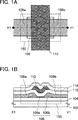
Als Beispiel für eine Halbleitervorrichtung ist ein Transistor mit obenliegendem Gate (top-gate transistor) in 1A und 1B gezeigt. 1A ist eine Draufsicht, und 1B ist eine Querschnittsansicht entlang der gestrichelten Linie X1-Y1 in 1A. Es sei angemerkt, dass einige Komponenten eines Transistors 150 (z. B. ein Gate-Isolierfilm 110) der Einfachheit halber in 1A wegfallen.As an example of a semiconductor device, a top-gate transistor is shown in FIG 1A and 1B shown. 1A is a top view, and 1B FIG. 12 is a cross-sectional view taken along the dashed line X1-Y1 in FIG 1A , It should be noted that some components of a transistor 150 (For example, a gate insulating film 110 ) for the sake of simplicity 1A eliminated.

Der Transistor 150 in 1A und 1B beinhaltet über einem Substrat 102 einen Basis-Isolierfilm 104, einen Oxidhalbleiterfilm 106, der über dem Basis-Isolierfilm 104 ausgebildet ist und einen Bereich 106a und einen Bereich 106b aufweist, eine Source-Elektrode 108a und eine Drain-Elektrode 108b, die über dem Basis-Isolierfilm 104 und dem Oxidhalbleiterfilm 106 ausgebildet sind, den Gate-Isolierfilm 110, der über dem Oxidhalbleiterfilm 106, der Source-Elektrode 108a und der Drain-Elektrode 108b ausgebildet ist, und eine Gate-Elektrode 112, die in Kontakt mit dem Gate-Isolierfilm 110 steht und zumindest mit dem Oxidhalbleiterfilm 106 überlappt. Außerdem ist ein Zwischenschicht-Isolierfilm 114 über dem Transistor 150 ausgebildet. The transistor 150 in 1A and 1B includes over a substrate 102 a base insulating film 104 , an oxide semiconductor film 106 that over the base insulating film 104 is formed and an area 106a and an area 106b comprising a source electrode 108a and a drain electrode 108b that over the base insulating film 104 and the oxide semiconductor film 106 are formed, the gate insulating film 110 that over the oxide semiconductor film 106 , the source electrode 108a and the drain electrode 108b is formed, and a gate electrode 112 in contact with the gate insulating film 110 is and at least with the oxide semiconductor film 106 overlaps. In addition, an interlayer insulating film 114 over the transistor 150 educated.

Die Dicke des Oxidhalbleiterfilms 106 ist größer als 5 nm und kleiner als oder gleich 200 nm, bevorzugt größer als oder gleich 10 nm und kleiner als oder gleich 30 nm. Außerdem hat der Oxidhalbleiterfilm 106 vorzugsweise eine Struktur mit Kristallinität (z. B. eine Einkristallstruktur, eine mikrokristalline Struktur oder dergleichen).The thickness of the oxide semiconductor film 106 is greater than 5 nm and less than or equal to 200 nm, preferably greater than or equal to 10 nm and less than or equal to 30 nm. In addition, the oxide semiconductor film 106 preferably, a structure having crystallinity (eg, a single crystal structure, a microcrystalline structure, or the like).

Wie in 1B gezeigt ist, verjüngt sich vorzugsweise ein Endbereich des Oxidhalbleiterfilms 106 unter einem Winkel von 20° bis 50°. Wenn der Oxidhalbleiterfilm 106 einen senkrechten Endbereich hat, wird Sauerstoff mit höherer Wahrscheinlichkeit von dem Endbereich des Oxidhalbleiterfilms 106 abgegeben; somit werden wahrscheinlich Sauerstofffehlstellen (oxygen vacancies) erzeugt. Wenn der Oxidhalbleiterfilm 106 einen sich verjüngenden Endbereich hat, wird eine Erzeugung von Sauerstofffehlstellen unterdrückt, und daher kann eine Erzeugung von Leckstrom des Transistors 150 verringert werden.As in 1B is shown, an end portion of the oxide semiconductor film preferably tapers 106 at an angle of 20 ° to 50 °. When the oxide semiconductor film 106 has a vertical end portion, oxygen is more likely to be from the end portion of the oxide semiconductor film 106 issued; thus, oxygen vacancies are likely to be generated. When the oxide semiconductor film 106 has a tapered end portion, generation of oxygen vacancies is suppressed, and therefore generation of leakage current of the transistor can be prevented 150 be reduced.

Bei dieser Ausführungsform ist der Oxidhalbleiterfilm 106 vorzugsweise ein Film aus einem kristallinen Oxidhalbleiter mit Ausrichtung bezüglich der c-Achse (c-axis aligned crystalline oxide semiconductor film: CAAC-OS-Film). Es sei angemerkt, dass der CAAC-OS-Film später ausführlich bei einem Herstellungsverfahren des Transistors 150 beschrieben wird.In this embodiment, the oxide semiconductor film is 106 Preferably, a c-axis aligned crystalline oxide semiconductor film (CAAC-OS film) crystalline oxide semiconductor film. It should be noted that the CAAC-OS film will be described later in detail in a manufacturing process of the transistor 150 is described.

Für den Gate-Isolierfilm 110 wird vorzugsweise ein Oxid, das Silizium enthält und eine ausreichende Spannungsfestigkeit (withstand voltage) und ausreichende isolierende Eigenschaften aufweist, verwendet. In dem Fall, in dem der Gate-Isolierfilm 110 eine einschichtige Struktur hat, kann beispielsweise ein Isolierfilm wie z. B. ein Siliziumoxidfilm verwendet werden.For the gate insulating film 110 For example, an oxide containing silicon and having sufficient withstand voltage and sufficient insulating properties is preferably used. In the case where the gate insulating film 110 has a single-layer structure, for example, an insulating film such. For example, a silicon oxide film may be used.

Alternativ kann der Gate-Isolierfilm 110 eine gestapelte Struktur aufweisen. In dem Fall, in dem der Gate-Isolierfilm 110 eine gestapelte Struktur aufweist, kann ein Oxid, das Silizium enthält, über einem Galliumoxid, einem Aluminiumoxid, einem Siliziumnitrid, einem Siliziumoxynitrid, einem Aluminiumoxynitrid, einem Yttriumoxid, einem Lanthanoxid, einem Siliziumnitridoxid oder dergleichen gestapelt werden. Alternativ kann ein Oxid, das Silizium enthält, über einem Material mit hohem k, wie z. B. Hafniumoxid, Hafniumsilikat (HfSixOy (x > 0, y > 0)), Hafniumsilikat, dem Stickstoff zugesetzt worden ist (HfSiOxNy (x > 0, y > 0)) oder Hafniumaluminat (HfAlxOy (x > 0, y > 0)) gestapelt werden.Alternatively, the gate insulating film 110 have a stacked structure. In the case where the gate insulating film 110 has a stacked structure, an oxide containing silicon may be stacked over a gallium oxide, an alumina, a silicon nitride, a silicon oxynitride, an aluminum oxynitride, an yttria, a lanthana, a silicon nitride, or the like. Alternatively, an oxide containing silicon may overlay a high-k material, such as silicon. Hafnium oxide, hafnium silicate (HfSi x O y (x> 0, y> 0)), hafnium silicate to which nitrogen has been added (HfSiO x N y (x> 0, y> 0)) or hafnium aluminate (HfAl x O y (x> 0, y> 0)) are stacked.

Im Fall der Verwendung eines Oxides, das Silizium enthält, als der Gate-Isolierfilm 110 kann ein Teil des enthaltenen Sauerstoffs von dem Isolierfilm abgegeben werden, wenn der Isolierfilm erwärmt wird. Daher kann Sauerstoff zu dem Oxidhalbleiterfilm 106 zugeführt werden, und Sauerstofffehlstellen in dem Oxidhalbleiterfilm 106 können gefüllt werden. Insbesondere enthält vorzugsweise der Gate-Isolierfilm 110 eine große Menge an Sauerstoff, die zumindest seine Stöchiometrie überschreitet. Beispielsweise wird ein Film von Siliziumoxid, das durch die Formel SiO2+α (α > 0) dargestellt wird, vorzugsweise als der Gate-Isolierfilm 110 verwendet. Wenn ein derartiger Siliziumoxidfilm als der Gate-Isolierfilm 110 verwendet wird, kann Sauerstoff zu dem Oxidhalbleiterfilm 106 zugeführt werden, so dass der Transistor 150, bei dem der Oxidhalbleiterfilm 106 verwendet wird, vorteilhafte Transistoreigenschaften aufweisen kann.In the case of using an oxide containing silicon as the gate insulating film 110 For example, part of the contained oxygen may be released from the insulating film when the insulating film is heated. Therefore, oxygen can be added to the oxide semiconductor film 106 and oxygen vacancies in the oxide semiconductor film 106 can be filled. In particular, preferably, the gate insulating film 110 a large amount of oxygen that exceeds at least its stoichiometry. For example, a film of silicon oxide represented by the formula SiO 2 + α (α> 0) is preferably used as the gate insulating film 110 used. When such a silicon oxide film as the gate insulating film 110 can be used, oxygen to the oxide semiconductor film 106 be supplied, so that the transistor 150 in which the oxide semiconductor film 106 used, may have advantageous transistor properties.

Jedoch könnte im Fall der Verwendung eines Siliziumoxidfilms als der Gate-Isolierfilm 110 Silizium, das ein Bestandteil des Gate-Isolierfilms 110 ist, als Verunreinigung in den Oxidhalbleiterfilm 106 aufgenommen werden. Silizium oder dergleichen, das ein Bestandteil des Gate-Isolierfilms 110 ist, dringt in den Oxidhalbleiterfilm 106 ein und dient als Verunreinigung, die die Eigenschaften des Transistors beeinflusst.However, in the case of using a silicon oxide film as the gate insulating film 110 Silicon, which is a part of the gate insulating film 110 is as an impurity in the oxide semiconductor film 106 be recorded. Silicon or the like, which is a part of the gate insulating film 110 is penetrates into the oxide semiconductor film 106 and serves as an impurity that affects the characteristics of the transistor.

Ferner dringt in dem Fall, in dem der Oxidhalbleiterfilm 106 ein CAAC-OS-Film ist, Silizium oder dergleichen, das ein Bestandteil des Gate-Isolierfilms 110 ist, in den Oxidhalbleiterfilm 106 ein, und eine Bindung in dem Kristallbereich in dem Oxidhalbleiterfilm 106 wird aufgebrochen. Deshalb werden mehr amorphe Bereiche in dem Oxidhalbleiterfilm 106 in der Nähe des Gate-Isolierfilms 110 ausgebildet.Further, in the case where the oxide semiconductor film penetrates 106 is a CAAC-OS film, silicon or the like which is a part of the gate insulating film 110 is in the oxide semiconductor film 106 and bonding in the crystal region in the oxide semiconductor film 106 is broken up. Therefore, more amorphous regions become in the oxide semiconductor film 106 near the gate insulating film 110 educated.

Insbesondere dringen wahrscheinlich Verunreinigungen wie z. B. Silizium in den Oxidhalbleiterfilm 106 in der Nähe des Gate-Isolierfilms 110 ein. Ein Kanalbildungsbereich des Transistors 150 wird in dem Oxidhalbleiterfilm 106 in der Nähe der Grenzfläche zu dem Gate-Isolierfilm 110 ausgebildet; somit könnten die Eigenschaften des Transistors 150 verändert werden, wenn Verunreinigungen wie z. B. Silizium in die Nähe der Grenzfläche zwischen dem Oxidhalbleiterfilm 106 und dem Gate-Isolierfilm 110 eindringen.In particular, probably penetrate impurities such. For example, silicon in the oxide semiconductor film 106 near the gate insulating film 110 one. A channel formation region of the transistor 150 is in the oxide semiconductor 106 near the interface with the gate insulating film 110 educated; thus, the properties of the transistor could be 150 be changed when contaminants such. For example, silicon near the interface between the oxide semiconductor film 106 and the gate insulating film 110 penetration.

Die Veränderung der Struktur des Oxidhalbleiterfilms 106, die auftritt, wenn SiO2, ein Oxid, das Silizium enthält, als Verunreinigung zugesetzt wird, wurde durch klassische Moleküldynamikrechnung (classical molecular dynamics calculation) untersucht. Die Ergebnisse werden anhand von 12A, 12B, 13A, 13B und 14 beschrieben. Es sei angemerkt, dass eine Simulierungssoftware „SCIGRESS ME”, die von Fujitsu Limited hergestellt wird, für die klassische Moleküldynamikrechnung verwendet wurde. Ein empirisches Potential, das die Wechselwirkung zwischen Atomen charakterisiert, wird bei dem klassischen Moleküldynamikverfahren definiert, so dass die Kraft, die auf jedes Atom einwirkt, geschätzt wird. Newtonsches Gesetz der Bewegung wird numerisch gelöst, wodurch Bewegung (zeitabhängige Veränderung (time-dependent change)) jedes Atoms deterministisch verfolgt werden kann.The change of the structure of the oxide semiconductor film 106 , which occurs when SiO 2 , an oxide containing silicon, is added as an impurity was studied by classical molecular dynamics calculation. The results are based on 12A . 12B . 13A . 13B and 14 described. It should be noted that a simulation software "SCIGRESS ME" manufactured by Fujitsu Limited was used for classical molecular dynamics calculation. An empirical potential that characterizes the interaction between atoms is defined in the classical molecular dynamics method, so that the force acting on each atom is estimated. Newton's law of motion is solved numerically, whereby movement (time-dependent change) of each atom can be tracked deterministically.

Nachstehend werden Berechnungsmodelle und Berechnungsbedingungen beschrieben. Es sei angemerkt, dass in dieser Berechnung das Born-Mayer-Huggins-Potential verwendet wurde.The following describes calculation models and calculation conditions. It should be noted that the Born-Mayer-Huggins potential was used in this calculation.

Eine Einkristallstruktur von InGaZnO4, das 1680 Atome hat (siehe 12A) und eine Struktur von InGaZnO4, das 1680 Atome hat, wobei 20 Atome eines jeden von In, Ga und Zn durch Silizium-(Si-)Atome ersetzt werden (Siehe 12B), wurden als Berechnungsmodelle ausgebildet. In dem Modell in 12B, in dem Ersatz durch Silizium (Si) durchgeführt wird, sind Siliziumatome mit 3,57 Atom-% (2,34 Gew.-%) enthalten. Ferner ist die Dichte des Modells des Einkristalls in 12A 6,36 g/cm3, und die Dichte des Modells in 12B, in dem Ersatz durch Si durchgeführt wird, ist 6,08 g/cm3.A single crystal structure of InGaZnO 4 , which has 1680 atoms (see 12A ) and a structure of InGaZnO 4 , which has 1680 atoms, replacing 20 atoms of each of In, Ga, and Zn with silicon (Si) atoms (See 12B ), were designed as calculation models. In the model in 12B in which replacement is performed by silicon (Si), silicon atoms are included at 3.57 atomic% (2.34 wt%). Further, the density of the model of the single crystal is in 12A 6.36 g / cm 3 , and the density of the model in 12B in which substitution by Si is performed is 6.08 g / cm 3 .

Bei 1727°C, was niedriger als der Schmelzpunkt des InGaZnO4-Einkristalls ist (ca. 2000°C laut der Schätzung durch die klassische Moleküldynamikrechnung), wurde eine Strukturentspannung 150 ps lang (Zeitschrittbreite 0,2 fs × 750000 Schritte) mit einem konstanten Druck (1 Atom) an den Berechnungsmodellen in 12A und 12B durch die klassische Moleküldynamikrechnung durchgeführt. Die radialen Verteilungsfunktionen g(r) der zwei Strukturen wurden berechnet. Es sei angemerkt, dass die radiale Verteilungsfunktion g(r) eine Funktion ist, die die Wahrscheinlichkeitsdichte von Atomen darstellt, die in einer Entfernung von r von einem Atom existieren. Wenn die Korrelation zwischen Atomen verschwindet, nähert sich g(r) an 1 an.At 1727 ° C, which is lower than the melting point of InGaZnO 4 single crystal (about 2000 ° C as estimated by classical molecular dynamics theory), a relaxation of structure became 150 ps long (time step 0.2 fs × 750,000 steps) with a constant Pressure (1 atom) on the calculation models in 12A and 12B performed by classical molecular dynamics. The radial distribution functions g (r) of the two structures were calculated. It should be noted that the radial distribution function g (r) is a function representing the probability density of atoms existing at a distance of r from one atom. When the correlation between atoms disappears, g (r) approaches unity.

13A und 13B zeigen letzte Strukturen, die durch die klassische Moleküldynamikrechnung an den obigen zwei Berechnungsmodellen für 150 ps erhalten wurden. Zusätzlich zeigt 14 die radiale Verteilungsfunktion g(r) bei jeder Struktur. 13A and 13B show last structures obtained by the classical molecular dynamics calculation on the above two calculation models for 150 ps. Additionally shows 14 the radial distribution function g (r) for each structure.

Das Modell des Einkristalls in 13A ist stabil und bewahrt die Kristallstruktur auch bei der letzten Struktur, während das Modell in 13B, in dem Ersatz durch Si durchgeführt wird, instabil ist. Es kann beobachtet werden, dass die Kristallstruktur mit der Zeit verzerrt wird und sich in eine amorphe Struktur verändert. Wenn die radialen Verteilungsfunktionen g(r) der Strukturmodelle in 14 miteinander verglichen werden, findet man, dass das Einkristallmodell auch in einer großen Entfernung Peaks aufweist und eine Fernordnung (long-range order) aufweist. Im Gegensatz dazu findet man, dass in dem Modell, in dem Ersatz durch Si durchgeführt wird, der Peak in einer Entfernung von 0,6 nm verschwindet, und das Modell, in dem Ersatz durch Si durchgeführt wird, keine Fernordnung aufweist.The model of the single crystal in 13A is stable and preserves the crystal structure even in the last structure, while the model in 13B in which replacement is performed by Si is unstable. It can be observed that the crystal structure is distorted over time and changes into an amorphous structure. If the radial distribution functions g (r) of the structural models in 14 are compared with each other, it is found that the single crystal model has peaks even at a long distance and has a long-range order. In contrast, it is found that in the model in which substitution by Si is performed, the peak disappears at a distance of 0.6 nm, and the model in which substitution by Si is performed does not have long-range order.

Die obigen Berechnungsergebnisse deuten darauf hin, dass dann, wenn Silizium (Si) in InGaZnO4 enthalten ist, InGaZnO4 wahrscheinlich amorph wird. Ferner wird derartiges InGaZnO4 laut der obigen Ergebnisse nicht kristallisiert, auch wenn InGaZnO4, das Silizium (Si) enthält, bei hoher Temperatur erwärmt wird.The above calculation results indicate that, when silicon (Si) is contained in InGaZnO 4 , InGaZnO 4 is likely to become amorphous. Further, such InGaZnO 4 is not crystallized according to the above results, although InGaZnO 4 containing silicon (Si) is heated at a high temperature.

Dann wurde eine Veränderung der Struktur des Oxidhalbleiterfilms 106, die auftritt, wenn Kohlenstoffatome (C) zugesetzt werden, durch die klassische Moleküldynamikrechnung untersucht. Die Ergebnisse werden anhand von 12A, 15A, 15B und 16 beschrieben. Es sei angemerkt, dass die Simulierungssoftware „SCIGRESS ME”, die von Fujitsu Limited hergestellt wird, für die klassische Moleküldynamikrechnung verwendet wurde.Then, a change of the structure of the oxide semiconductor film became 106 that occurs when carbon atoms (C) are added are studied by classical molecular dynamics theory. The results are based on 12A . 15A . 15B and 16 described. It should be noted that the simulation software "SCIGRESS ME" manufactured by Fujitsu Limited was used for classical molecular dynamics calculation.

Berechnungsmodelle und Berechnungsbedingungen sind wie folgt. Es sei angemerkt, dass in dieser Berechnung das Born-Mayer-Huggins-Potential verwendet wurde. Des Weiteren wurde für die Wechselwirkung zwischen Kohlenstoffatomen (C) ein Lennard-Jones-Potential verwendet.Calculation models and calculation conditions are as follows. It should be noted that the Born-Mayer-Huggins potential was used in this calculation. Furthermore, a Lennard-Jones potential was used for the interaction between carbon atoms (C).

Eine Einkristallstruktur von InGaZnO4, das 1680 Atome hat (siehe 12A) und eine Struktur von InGaZnO4, das 1680 Atome hat, wobei 20 Atome eines jeden von In, Ga und Zn durch Kohlenstoffatome (C) ersetzt werden und 80 Atome von Sauerstoff (O) durch Kohlenstoffatome (C) ersetzt werden (siehe 15A), wurden als Berechnungsmodelle ausgebildet. In dem Modell in 15A, in dem Ersatz durch C durchgeführt wird, sind Kohlenstoffatome (C) mit 8,33 Atom-% enthalten. Ferner ist die Dichte des Modells des Einkristalls in 12A 6,36 g/cm3, und die Dichte des Modells in 15A, in dem Ersatz durch C durchgeführt wird, ist 5,89 g/cm3. A single crystal structure of InGaZnO 4 , which has 1680 atoms (see 12A and a structure of InGaZnO 4 having 1680 atoms, replacing 20 atoms of each of In, Ga, and Zn with carbon atoms (C) and replacing 80 atoms of oxygen (O) with carbon atoms (C) (see 15A ), were designed as calculation models. In the model in 15A in which replacement is performed by C, carbon atoms (C) are contained at 8.33 at%. Further, the density of the model of the single crystal is in 12A 6.36 g / cm 3 , and the density of the model in 15A in which replacement is performed by C is 5.89 g / cm 3 .

Bei 1727°C, was niedriger als der Schmelzpunkt des InGaZnO4-Einkristalls ist (ca. 2000°C laut der Schätzung durch die klassische Moleküldynamikrechnung), wurde eine Strukturentspannung 150 ps lang (Zeitschrittbreite 0,2 fs × 750000 Schritte) mit einem konstanten Druck (1 Atom) an den Berechnungsmodellen in 12A und 15A durch die klassische Moleküldynamikrechnung durchgeführt. Die radialen Verteilungsfunktionen g(r) der zwei Strukturen wurden gerechnet. Es sei angemerkt, dass die radiale Verteilungsfunktion g(r) eine Funktion ist, die die Wahrscheinlichkeitsdichte von Atomen darstellt, die in einer Entfernung von r von einem Atom existieren. Wenn die Korrelation zwischen Atomen verschwindet, nähert sich g(r) an 1 an.At 1727 ° C, which is lower than the melting point of InGaZnO 4 single crystal (about 2000 ° C as estimated by classical molecular dynamics theory), a relaxation of structure became 150 ps long (time step 0.2 fs × 750,000 steps) with a constant Pressure (1 atom) on the calculation models in 12A and 15A performed by classical molecular dynamics. The radial distribution functions g (r) of the two structures were calculated. It should be noted that the radial distribution function g (r) is a function representing the probability density of atoms existing at a distance of r from one atom. When the correlation between atoms disappears, g (r) approaches unity.

13A und 15B zeigen letzte Strukturen, die durch die klassische Moleküldynamikrechnung an den obigen zwei Berechnungsmodellen für 150 ps erhalten wurden. Die radiale Verteilungsfunktion g(r) bei jeder Struktur ist in 16 gezeigt. 13A and 15B show last structures obtained by the classical molecular dynamics calculation on the above two calculation models for 150 ps. The radial distribution function g (r) in each structure is in 16 shown.

Das Modell des Einkristalls in 13A ist stabil und bewahrt die Kristallstruktur auch bei der letzten Struktur, während das Modell in 15B, in dem Ersatz durch C durchgeführt wird, instabil ist. Es kann beobachtet werden, dass die Kristallstruktur mit der Zeit verzerrt wird und sich in eine amorphe Struktur verändert. Durch Vergleichen der radialen Verteilungsfunktionen g(r) der Strukturmodelle miteinander wie in 16 findet man, dass das Einkristallmodell auch in einer großen Entfernung Peaks aufweist und die Fernordnung aufweist. Im Gegensatz dazu findet man, dass in dem Modell, in dem Ersatz durch C durchgeführt wird, der Peak in einer Entfernung von 0,7 nm verschwindet, und das Modell, in dem Ersatz durch C durchgeführt wird, keine Fernordnung aufweist.The model of the single crystal in 13A is stable and preserves the crystal structure even in the last structure, while the model in 15B in which replacement is performed by C is unstable. It can be observed that the crystal structure is distorted over time and changes into an amorphous structure. By comparing the radial distribution functions g (r) of the structural models with each other as in 16 it is found that the single-crystal model also peaks at a great distance and has the long-range order. In contrast, it is found that in the model in which replacement is performed by C, the peak disappears at a distance of 0.7 nm and the model in which replacement is performed by C does not have long-range ordering.

Die obigen Berechnungsergebnisse deuten darauf hin, dass dann, wenn Kohlenstoff (C) in InGaZnO4 enthalten ist, InGaZnO4 wahrscheinlich amorph wird. Ferner wird derartiges InGaZnO4 laut der obigen Ergebnisse nicht kristallisiert, auch wenn InGaZnO4, das Kohlenstoff (C) enthält, bei hoher Temperatur erwärmt wird.The above calculation results indicate that when carbon (C) is contained in InGaZnO 4 , InGaZnO 4 is likely to become amorphous. Further, such InGaZnO 4 is not crystallized according to the above results, although InGaZnO 4 containing carbon (C) is heated at a high temperature.

Daher wird in der Halbleitervorrichtung, die bei dieser Ausführungsform beschrieben wird, das Eindringen von Verunreinigungen wie z. B. Silizium in den Oxidhalbleiterfilm 106 in der Nähe der Grenzfläche zu dem Gate-Isolierfilm 110 unterdrückt. Folglich wird in dem Oxidhalbleiterfilm 106 ein Bereich ausgebildet, in dem die Konzentration von Silizium, das von einer Grenzfläche zu dem Gate-Isolierfilm 110 zum Inneren des Oxidhalbleiterfilms 106 hin verteilt ist, niedriger als oder gleich 1,0 Atom-% ist. Ein derartiger Bereich wird wie in 1B ein Bereich 106a genannt. Die Siliziumkonzentration in dem Bereich 106a ist stärker bevorzugt niedriger als oder gleich 0,1 Atom-%. Außerdem wird der Bereich 106a in Kontakt mit dem Gate-Isolierfilm 110 bereitgestellt und hat eine Dicke von kleiner als oder gleich 5 nm.Therefore, in the semiconductor device described in this embodiment, the intrusion of impurities such as e.g. For example, silicon in the oxide semiconductor film 106 near the interface with the gate insulating film 110 suppressed. As a result, in the oxide semiconductor film 106 formed a region in which the concentration of silicon, that from an interface to the gate insulating film 110 to the inside of the oxide semiconductor film 106 is less than or equal to 1.0 atomic%. Such an area becomes as in 1B an area 106a called. The silicon concentration in the range 106a More preferably, it is lower than or equal to 0.1 at%. In addition, the area becomes 106a in contact with the gate insulating film 110 provided and has a thickness of less than or equal to 5 nm.

Es sei angemerkt, dass, wie in 1B, ein Bereich in dem Oxidhalbleiterfilm 106, der verschieden von dem Bereich 106a ist, ein Bereich 106b genannt wird.It should be noted that, as in 1B a region in the oxide semiconductor film 106 that is different from the area 106a is, an area 106b is called.

In dem Fall, in dem ferner Verunreinigungen wie z. B. Kohlenstoff in dem Gate-Isolierfilm 110 enthalten sind, könnten solche Verunreinigungen auch in den Oxidhalbleiterfilm 106 eindringen und dienen als Verunreinigungen, wie beim Fall von Silizium. In diesem Fall ist die Konzentration von Kohlenstoff in dem Bereich 106a niedriger als oder gleich 1,0 × 10²⁰ Atome/cm3, bevorzugt niedriger als oder gleich 1,0 × 10¹⁹ Atome/cm3.In the case in which further impurities such. For example, carbon in the gate insulating film 110 may contain such impurities in the oxide semiconductor film 106 penetrate and serve as impurities, as in the case of silicon. In this case, the concentration of carbon is in the range 106a lower than or equal to 1.0 x 10 20 atoms / cm 3 , preferably lower than or equal to 1.0 x 10 19 atoms / cm 3 .

Um zu verhindern, dass Verunreinigungen wie z. B. Silizium in den Oxidhalbleiterfilm 106 eindringen, kann der Gate-Isolierfilm derart ausgebildet werden, dass der Oxidhalbleiterfilm 106 nicht beschädigt wird. In dem Fall, in dem beispielsweise ein Siliziumoxidfilm als der Gate-Isolierfilm 110 durch ein Sputterverfahren ausgebildet wird, kann die Auswirkung von Silizium (das ein Bestandteil des Gate-Isolierfilms 110 ist), das mit dem Oxidhalbleiterfilm 106 kollidiert, verringert werden. Damit man den obigen Effekt erzielen kann, kann man beispielsweise das Folgende verwenden: ein Verfahren, bei dem die Leistung zur Abscheidung des Gate-Isolierfilms 110 niedrig ist, ein Verfahren, bei dem der Druck zur Abscheidung des Gate-Isolierfilms 110 hoch ist, ein Verfahren, bei dem eine Distanz zwischen einem Target und einem Substrat (T-S-Distanz) bei der Abscheidung des Gate-Isolierfilms 110 verlängert wird, oder dergleichen. Jedoch ist ein Verfahren zum Ausbilden des Gate-Isolierfilms 110 nicht auf die obigen Verfahren beschränkt. Beispielsweise kann ein Siliziumoxidfilm, ein Siliziumoxynitridfilm, ein Siliziumnitridoxidfilm oder dergleichen, der durch ein PE-CVD-Verfahren ausgebildet wird, verwendet werden. Ein PE-CVD-Verfahren wird gegenüber einem Sputterverfahren bevorzugt, weil unter Verwendung des PE-CVD-Verfahrens der Oxidhalbleiterfilm 106, der als Basisfilm dient, weniger beschädigt wird.To prevent contaminants such. For example, silicon in the oxide semiconductor film 106 penetrate, the gate insulating film may be formed such that the oxide semiconductor film 106 not damaged. In the case where, for example, a silicon oxide film is used as the gate insulating film 110 is formed by a sputtering process, the effect of silicon (which is a component of the gate insulating film 110 ) with the oxide semiconductor film 106 collides, be reduced. For example, to obtain the above effect, one can use the following: a method in which the performance for depositing the gate insulating film 110 is low, a method in which the pressure for depositing the gate insulating film 110 is high, a method in which a distance between a target and a substrate (TS distance) in the deposition of the gate insulating film 110 is extended, or the like. However, a method of forming the gate insulating film is 110 not limited to the above methods. For example, a silicon oxide film, a Silicon oxynitride film, a silicon nitride oxide film or the like formed by a PE-CVD method. A PE-CVD method is preferred over a sputtering method because, using the PE-CVD method, the oxide semiconductor film 106 , which serves as a base film, less damaged.

Wie oben beschrieben worden ist, wird die Konzentration von Verunreinigungen wie z. B. Silizium und Kohlenstoff, die in den Bereich 106a in dem Oxidhalbleiterfilm 106 eindringen, verringert, wodurch eine Veränderung der Eigenschaften des Transistors 150 unterdrückt werden kann. Ferner kann in dem Fall, in dem der Oxidhalbleiterfilm 106 ein CAAC-OS-Film ist, ein Kristallbereich auch in der Nähe des Gate-Isolierfilms 110 ausgebildet werden. Wenn der Transistor 150 unter Verwendung eines derartigen Oxidhalbleiterfilms 106 ausgebildet wird, kann eine Halbleitervorrichtung mit stabilen elektrischen Eigenschaften bereitgestellt werden.As described above, the concentration of impurities such. As silicon and carbon in the area 106a in the oxide semiconductor film 106 penetrate, reducing, causing a change in the properties of the transistor 150 can be suppressed. Further, in the case where the oxide semiconductor film 106 a CAAC-OS film is a crystal region also near the gate insulating film 110 be formed. When the transistor 150 using such an oxide semiconductor film 106 is formed, a semiconductor device having stable electrical characteristics can be provided.

Es sei angemerkt, dass die Details der anderen Komponenten des Transistors anhand von 2A bis 2D beim Beschreiben eines Verfahrens zum Herstellen des Transistors 150 nachstehend beschrieben werden.It should be noted that the details of the other components of the transistor based on 2A to 2D in describing a method of manufacturing the transistor 150 will be described below.

<Herstellungsverfahren des Transistors 150><Production method of the transistor 150 >

Nachstehend wird ein Beispiel für ein Verfahren zum Herstellen des Transistors 150 in 1A und 1B dieser Ausführungsform anhand von 2A bis 2D beschrieben.Below is an example of a method of manufacturing the transistor 150 in 1A and 1B this embodiment with reference to 2A to 2D described.

Zuerst wird das Substrat 102 vorbereitet. Es gibt zwar keine bestimmte Begrenzung auf ein Substrat, das als das Substrat 102 verwendet werden kann, es ist jedoch nötig, dass das Substrat Wärmebeständigkeit aufweist, mit der es später zumindest eine Wärmebehandlung aushalten kann. Beispielsweise kann ein Glassubstrat wie z. B. ein Bariumborosilikatglassubstrat oder ein Alumoborosilikatglassubstrat, ein Keramiksubstrat, ein Quarzsubstrat, ein Saphirsubstrat oder dergleichen verwendet werden. Alternativ kann ein einkristallines Halbleitersubstrat oder ein polykristallines Halbleitersubstrat aus Silizium oder Siliziumkarbid, ein Verbund-Halbleitersubstrat aus Siliziumgermanium oder dergleichen, ein SOI-Substrat oder dergleichen verwendet werden.First, the substrate 102 prepared. While there is no particular limitation on a substrate, as the substrate 102 can be used, but it is necessary that the substrate has heat resistance, with which it can endure at least one heat treatment later. For example, a glass substrate such. For example, a barium borosilicate glass substrate or an aluminoborosilicate glass substrate, a ceramic substrate, a quartz substrate, a sapphire substrate or the like may be used. Alternatively, a single-crystalline semiconductor substrate or a polycrystalline semiconductor substrate of silicon or silicon carbide, a compound semiconductor substrate of silicon germanium or the like, an SOI substrate or the like may be used.

Ein flexibles Substrat kann als das Substrat 102 verwendet werden. Im Fall der Verwendung eines flexiblen Substrats kann ein Transistor, der den Oxidhalbleiterfilm 106 beinhaltet, direkt über dem flexiblen Substrat ausgebildet werden. Alternativ kann ein Transistor, der den Oxidhalbleiterfilm 106 beinhaltet, über einem anderen Substrat ausgebildet werden und dann kann der Transistor abgetrennt und zu einem flexiblen Substrat versetzt werden. Damit man den Transistor von dem Substrat abtrennen und zu dem flexiblen Substrat versetzen kann, kann eine Trennschicht zwischen dem Substrat und dem Transistor, der den Oxidhalbleiterfilm 106 beinhaltet, angeordnet werden.A flexible substrate may be considered the substrate 102 be used. In the case of using a flexible substrate, a transistor including the oxide semiconductor film 106 includes formed directly over the flexible substrate. Alternatively, a transistor including the oxide semiconductor film 106 can be formed over another substrate and then the transistor can be separated and added to a flexible substrate. In order to separate the transistor from the substrate and allow it to move to the flexible substrate, a separating layer may be formed between the substrate and the transistor including the oxide semiconductor film 106 includes, be arranged.

Als Nächstes wird der Basis-Isolierfilm 104 über dem Substrat 102 ausgebildet (siehe 2A). Der Basis-Isolierfilm 104 hat einen Effekt, dass er die Diffusion eines Verunreinigungselements wie z. B. Wasserstoff oder Feuchtigkeit aus dem Substrat 102 verhindert, und kann mit einer einschichtigen Struktur oder einer gestapelten Struktur, die einen oder mehrere von einem Siliziumnitridfilm, einem Siliziumoxidfilm, einem Siliziumnitridoxidfilm und einem Siliziumoxynitridfilm verwendet, ausgebildet werden.Next, the base insulating film becomes 104 above the substrate 102 trained (see 2A ). The base insulating film 104 has an effect of preventing the diffusion of a contaminant such as e.g. As hydrogen or moisture from the substrate 102 and can be formed with a single-layered structure or a stacked structure using one or more of a silicon nitride film, a silicon oxide film, a silicon nitride oxide film, and a silicon oxynitride film.

Darüber hinaus kann als anderer Effekt des Basis-Isolierfilms 104 Sauerstoff zu dem später ausgebildeten Oxidhalbleiterfilm 106 zugeführt werden. Beispielsweise kann in dem Fall, in dem ein Isolierfilm, der ein Oxid enthält, als der Basis-Isolierfilm 104 ausgebildet wird, ein Teil enthaltenen Sauerstoffs durch Erwärmung des Basis-Isolierfilms 104 abgegeben werden. Daher kann Sauerstoff zu dem Oxidhalbleiterfilm 106 zugeführt werden, und Sauerstofffehlstellen in dem Oxidhalbleiterfilm 106 können somit gefüllt werden. Insbesondere enthält vorzugsweise der Basis-Isolierfilm 104 eine große Menge an Sauerstoff, die zumindest seine Stöchiometrie überschreitet. Beispielsweise wird ein Film von Siliziumoxid, das durch die Formel SiO2+α (α > 0) dargestellt wird, vorzugsweise als der Basis-Isolierfilm 104 verwendet. Wenn ein derartiger Siliziumoxidfilm als der Basis-Isolierfilm 104 verwendet wird, kann Sauerstoff zu dem Oxidhalbleiterfilm 106 zugeführt werden, so dass der Transistor 150, bei dem der Oxidhalbleiterfilm 106 verwendet wird, vorteilhafte Transistoreigenschaften aufweisen kann.In addition, as a different effect of the base insulating film 104 Oxygen to the later formed oxide semiconductor film 106 be supplied. For example, in the case where an insulating film containing an oxide may be used as the base insulating film 104 a portion of contained oxygen is formed by heating the base insulating film 104 be delivered. Therefore, oxygen can be added to the oxide semiconductor film 106 and oxygen vacancies in the oxide semiconductor film 106 can thus be filled. In particular, preferably, the base insulating film contains 104 a large amount of oxygen that exceeds at least its stoichiometry. For example, a film of silicon oxide represented by the formula SiO 2 + α (α> 0) is preferably used as the base insulating film 104 used. When such a silicon oxide film as the base insulating film 104 can be used, oxygen to the oxide semiconductor film 106 be supplied, so that the transistor 150 in which the oxide semiconductor film 106 used, may have advantageous transistor properties.

Bevor der Basis-Isolierfilm 104 ausgebildet wird, kann eine Plasmabehandlung oder dergleichen an dem Substrat 102 durchgeführt werden. Als Plasmabehandlung kann ein umgekehrtes Sputtern, bei dem ein Argongas eingeführt wird und Plasma erzeugt wird, durchgeführt werden. Das umgekehrte Sputtern ist ein Verfahren, bei dem eine HF-Leistungsquelle zum Anlegen einer Spannung an die Substrat 102-Seite in einer Argon-Atmosphäre verwendet wird, so dass Plasma in der Nähe des Substrats 102 erzeugt wird, um eine Oberfläche des Substrats zu modifizieren. Es sei angemerkt, dass statt einer Argon-Atmosphäre eine Stickstoff-Atmosphäre, eine Helium-Atmosphäre, eine Sauerstoff-Atmosphäre oder dergleichen verwendet werden kann. Das umgekehrte Sputtern kann teilchenförmige Substanzen (auch als Partikel oder Staub bezeichnet), die an der Oberfläche des Substrats 102 haften, entfernen.Before the base insulating film 104 is formed, a plasma treatment or the like on the substrate 102 be performed. As the plasma treatment, reverse sputtering in which an argon gas is introduced and plasma is generated can be performed. Inverse sputtering is a process in which an RF power source is used to apply a voltage to the substrate 102 Page in one Argon atmosphere is used, allowing plasma near the substrate 102 is generated to modify a surface of the substrate. It should be noted that instead of an argon atmosphere, a nitrogen atmosphere, a helium atmosphere, an oxygen atmosphere or the like may be used. The reverse sputtering may be particulate substances (also referred to as particles or dust) attached to the surface of the substrate 102 stick, remove.

Als Nächstes wird der Oxidhalbleiterfilm 106 über dem Basis-Isolierfilm 104 ausgebildet (siehe 2A). Der Oxidhalbleiterfilm 106 ist vorzugsweise ein CAAC-OS-Film. Es sei angemerkt, dass der Basis-Isolierfilm 104 und der Oxidhalbleiterfilm 106 vorzugsweise sukzessiv ausgebildet werden, ohne der Luft ausgesetzt zu werden.Next, the oxide semiconductor film 106 above the base insulating film 104 trained (see 2A ). The oxide semiconductor film 106 is preferably a CAAC-OS movie. It should be noted that the base insulating film 104 and the oxide semiconductor film 106 preferably be formed successively without being exposed to the air.

Der CAAC-OS-Film, der für den Oxidhalbleiterfilm 106 verwendet werden kann, wird nachstehend detailliert beschrieben.The CAAC-OS film used for the oxide semiconductor film 106 will be described in detail below.

Der CAAC-OS-Film ist weder vollständig einkristallin noch vollständig amorph. Der CAAC-OS-Film ist ein Oxidhalbleiterfilm mit einer kristallinen/amorphen Mischphasenstruktur, bei der Kristallbereiche in einer amorphen Phase eingeschlossen sind. Es sei angemerkt, dass in den meisten Fällen der Kristallbereich in einen Würfel mit einer Kantenlänge von weniger als 100 nm passt. Aus einem mit einem Transmissionselektronenmikroskop (TEM) erhaltenen Beobachtungsbild wird in dem CAAC-OS-Film eine Grenze zwischen einem amorphen Bereich und einem Kristallbereich nicht deutlich. Außerdem wird mittels TEM in dem CAAC-OS-Film keine Korngrenze erkannt. Folglich ist in dem CAAC-OS-Film eine Verringerung der Elektronenbeweglichkeit, die der Korngrenze zugeschrieben wird, unterdrückt.The CAAC-OS film is neither completely single crystalline nor completely amorphous. The CAAC-OS film is an oxide semiconductor film having a crystalline / amorphous mixed phase structure in which crystal regions are enclosed in an amorphous phase. It should be noted that in most cases the crystal region fits into a cube with an edge length of less than 100 nm. From a observation image obtained by a transmission electron microscope (TEM), a boundary between an amorphous region and a crystal region does not become apparent in the CAAC-OS film. In addition, no grain boundary is detected by TEM in the CAAC-OS film. Consequently, in the CAAC-OS film, a reduction in electron mobility attributed to the grain boundary is suppressed.

Bei jedem der in dem CAAC-OS-Film eingeschlossenen Kristallbereiche ist eine c-Achse in einer Richtung ausgerichtet, die parallel zu einem Normalenvektor einer Oberfläche ist, auf der der CAAC-OS-Film ausgebildet ist, oder parallel zu einem Normalenvektor einer Oberfläche des CAAC-OS-Films ist, eine dreieckige oder hexagonale Atomanordnung, gesehen aus der Richtung, die senkrecht zur a-b-Fläche ist, ist ausgebildet und Metallatome sind in einer geschichteten Weise angeordnet oder Metallatome und Sauerstoffatome sind in einer geschichteten Weise angeordnet, gesehen aus der Richtung, die senkrecht zur c-Achse ist. Es sei angemerkt, dass bei den Kristallbereichen die Richtungen einer a-Achse und einer b-Achse eines Kristallbereichs unterschiedlich von denjenigen eines anderen Kristallbereichs sein können. In dieser Beschreibung und dergleichen umfasst der einfache Ausdruck „senkrecht” einen Bereich von 85° bis 95°. Außerdem umfasst der einfache Ausdruck „parallel” einen Bereich von –5° bis 5°.In each of the crystal regions included in the CAAC-OS film, a c-axis is aligned in a direction parallel to a normal vector of a surface on which the CAAC-OS film is formed, or parallel to a normal vector of a surface of the surface CAAC-OS film is a triangular or hexagonal atom arrangement as viewed from the direction perpendicular to the ab surface, is formed, and metal atoms are arranged in a layered manner, or metal atoms and oxygen atoms are arranged in a layered manner as viewed in FIG Direction that is perpendicular to the c-axis. It should be noted that, in the crystal regions, the directions of an a-axis and a b-axis of one crystal region may be different from those of another crystal region. In this specification and the like, the simple term "perpendicular" includes a range of 85 ° to 95 °. In addition, the simple term "parallel" includes a range of -5 ° to 5 °.

In dem CAAC-OS-Film ist die Verteilung der Kristallbereiche nicht unbedingt gleichmäßig. Beispielsweise ist in dem Fall, in dem beim Ausbildungsprozess des CAAC-OS-Films das Kristallwachstum von einer Oberflächenseite des Oxidhalbleiterfilms aus stattfindet, der Anteil der Kristallbereiche in der Nähe der Oberfläche des Oxidhalbleiterfilms in einigen Fällen höher als derjenige in der Nähe einer Oberfläche, auf der der Oxidhalbleiterfilm ausgebildet ist.In the CAAC-OS film, the distribution of the crystal areas is not necessarily uniform. For example, in the case where crystal growth occurs from a surface side of the oxide semiconductor film in the formation process of the CAAC-OS film, the proportion of the crystal regions near the surface of the oxide semiconductor film is higher in some cases than near a surface the oxide semiconductor film is formed.

Da die c-Achsen der in dem CAAC-OS-Film enthaltenen Kristallbereiche in der Richtung ausgerichtet sind, die parallel zu einem Normalenvektor einer Oberfläche, auf der der CAAC-OS-Film ausgebildet ist, oder parallel zu einem Normalenvektor einer Oberfläche des CAAC-OS-Films ist, können sich in Abhängigkeit von der Form des CAAC-OS-Films (der Querschnittsform der Oberfläche, auf der der CAAC-OS-Film ausgebildet ist, oder der Querschnittsform der Oberfläche des CAAC-OS-Films) die Richtungen der c-Achsen voneinander unterscheiden. Es sei angemerkt, dass dann, wenn der CAAC-OS-Film ausgebildet wird, die Richtung der c-Achse des Kristallbereichs eine Richtung ist, die parallel zu einem Normalenvektor der Oberfläche, auf der der CAAC-OS-Film ausgebildet ist, oder parallel zu einem Normalenvektor der Oberfläche des CAAC-OS-Films ist. Der Kristallbereich wird durch die Filmausbildung oder durch eine Behandlung zur Kristallbildung, wie z. B. eine Wärmebehandlung nach der Filmausbildung, gebildet.Since the c-axes of the crystal regions included in the CAAC-OS film are aligned in the direction parallel to a normal vector of a surface on which the CAAC-OS film is formed, or parallel to a normal vector of a surface of the CAAC-OS film. Depending on the shape of the CAAC-OS film (the cross-sectional shape of the surface on which the CAAC-OS film is formed, or the cross-sectional shape of the surface of the CAAC-OS film), the directions of the films may be OSC films c-axes differ from each other. It should be noted that when the CAAC-OS film is formed, the direction of the c-axis of the crystal region is a direction parallel to a normal vector of the surface on which the CAAC-OS film is formed, or in parallel to a normal vector of the surface of the CAAC-OS film. The crystal region is formed by the film formation or by a treatment for crystal formation, such. As a heat treatment after film formation formed.

Unter Verwendung des CAAC-OS Films in einem Transistor kann eine Veränderung der elektrischen Eigenschaften des Transistors aufgrund von Bestrahlung mit sichtbarem Licht oder UV-Licht verringert werden. Eine Veränderung und Schwankungen der Schwellenspannung können unterdrückt werden. Somit hat der Transistor eine hohe Zuverlässigkeit.By using the CAAC-OS film in a transistor, a change in the electrical characteristics of the transistor due to irradiation with visible light or UV light can be reduced. A change and fluctuation of the threshold voltage can be suppressed. Thus, the transistor has high reliability.

In einem Oxidhalbleiter, der eine Kristallinität besitzt (einem kristallinen Oxidhalbleiter), können Defekte in dem Bulk weiter reduziert werden. Ferner kann dann, wenn die Oberflächenglattheit des kristallinen Oxidhalbleiterfilms erhöht wird, ein Transistor mit obenliegendem Gate (top-gate transistor), der einen derartigen Oxidhalbleiter aufweist, höhere Feld-Effekt-Beweglichkeit erzielen, als ein Transistor, der einen amorphen Oxidhalbleiter aufweist. Um die Oberflächenglattheit des Oxidhalbleiterfilms zu erhöhen, wird der Oxidhalbleiter vorzugsweise über einer glatten Oberfläche ausgebildet. Insbesondere wird der Oxidhalbleiter vorzugsweise über einer Oberfläche mit einer durchschnittlichen Oberflächenrauheit (Ra) von weniger als oder gleich 0,15 nm, bevorzugt weniger als oder gleich 0,1 nm ausgebildet.In an oxide semiconductor having a crystallinity (a crystalline oxide semiconductor), defects in the bulk can be further reduced. Further, when the surface smoothness of the crystalline oxide semiconductor film is increased, a top gate transistor having such an oxide semiconductor can achieve higher field effect mobility than a transistor having an amorphous one Having oxide semiconductor. In order to increase the surface smoothness of the oxide semiconductor film, the oxide semiconductor is preferably formed over a smooth surface. In particular, the oxide semiconductor is preferably formed over a surface having an average surface roughness (R a ) of less than or equal to 0.15 nm, preferably less than or equal to 0.1 nm.

Es sei angemerkt, dass die durchschnittliche Oberflächenrauheit (Ra) durch eine dreidimensionale Erweiterung einer arithmetischen mittleren Oberflächenrauheit derart, dass sie auf eine gekrümmte Oberfläche angewendet werden kann, erhalten wird. Die Ra kann als ein ”Mittelwert der Absolutwerte der Abweichungen von einer Referenzoberfläche zu einer bestimmten Oberfläche” ausgedrückt werden und ist durch die folgende Formel definiert. [FORMEL 1]

Figure DE112012007290B3_0002
It should be noted that the average surface roughness (R a ) is obtained by a three-dimensional extension of an arithmetic mean surface roughness such that it can be applied to a curved surface. The R a can be expressed as an "average of the absolute values of the deviations from a reference surface to a certain surface" and is defined by the following formula. [FORMULA 1]
Figure DE112012007290B3_0002

Die bestimmte Oberfläche ist hier eine Oberfläche, die ein Gegenstand der Rauheitsmessung ist, wobei sie ein viereckiges Gebiet ist, das von vier durch die Koordinaten (x1, y1, f(x1, y1)), (x1, y2, f(x1, y2)), (x2, y1, f(x2, y1)) und (x2, y2, f(x2, y2)) bezeichneten Punkten dargestellt ist. Darüber hinaus stellt So die Fläche eines Rechtecks, das durch Projizieren der bestimmten Oberfläche auf die x-y Fläche erhalten ist, dar und Z0 stellt die Höhe der Bezugsoberfläche (die durchschnittliche Höhe der bestimmten Oberfläche) dar. Die Ra kann unter Verwendung eines Rasterkraftmikroskops (atomic force microsope: AFM) gemessen werden.The particular surface here is a surface which is an object of roughness measurement, being a quadrilateral area divided into four by the coordinates (x 1 , y 1 , f (x 1 , y 1 )), (x 1 , y 2 , f (x 1 , y 2 )), (x 2 , y 1 , f (x 2 , y 1 )) and (x 2 , y 2 , f (x 2 , y 2 )). In addition, So represents the area of a rectangle obtained by projecting the specific surface on the xy surface, and Z 0 represents the height of the reference surface (the average height of the particular surface). The R a can be calculated using an atomic force microscope (FIG. atomic force microsope: AFM).

Ein Oxidhalbleiter, der für den Oxidhalbleiterfilm 106 verwendet wird, enthält vorzugsweise zumindest Indium (In) oder Zink (Zn). Insbesondere sind vorzugsweise In und Zn enthalten. Als Stabilisator zur Verringerung von Schwankungen der elektrischen Eigenschaften eines Transistors, der den Oxidhalbleiterfilm aufweist, ist vorzugsweise zusätzlich Gallium (Ga) enthalten. Zinn (Sn) ist vorzugsweise als Stabilisator enthalten. Zudem ist vorzugsweise als Stabilisator ein oder mehrere Elemente enthalten, die aus Hafnium (Hf), Zirkonium (Zr), Titan (Ti), Scandium (Sc), Yttrium (Y) und einem Lanthanoidelement (wie z. B. Cer (Ce), Neodym (Nd) oder Gadolinium (Gd)) ausgewählt werden.An oxide semiconductor used for the oxide semiconductor film 106 is used, preferably contains at least indium (In) or zinc (Zn). In particular, In and Zn are preferably contained. As a stabilizer for reducing variations in electrical characteristics of a transistor having the oxide semiconductor film, gallium (Ga) is preferably additionally contained. Tin (Sn) is preferably included as a stabilizer. In addition, it is preferable to contain as the stabilizer one or more elements composed of hafnium (Hf), zirconium (Zr), titanium (Ti), scandium (Sc), yttrium (Y), and a lanthanoid element (such as cerium (Ce)). , Neodymium (Nd) or gadolinium (Gd)).

Als Oxidhalbleiter kann beispielsweise eines der Folgenden verwendet werden: Indiumoxid, Zinnoxid, Zinkoxid, ein Oxid auf In-Zn-Basis, ein Oxid auf Sn-Zn-Basis, ein Oxid auf Al-Zn-Basis, ein Oxid auf Zn-Mg-Basis, ein Oxid auf Sn-Mg-Basis, ein Oxid auf In-Mg-Basis, ein Oxid auf In-Ga-Basis, ein Oxid auf In-Ga-Zn-Basis (auch als IGZO bezeichnet), ein Oxid auf In-Al-Zn-Basis, ein Oxid auf In-Sn-Zn-Basis, ein Oxid auf Sn-Ga-Zn-Basis, ein Oxid auf Al-Ga-Zn-Basis, ein Oxid auf Sn-Al-Zn-Basis, ein Oxid auf In-Hf-Zn-Basis, ein Oxid auf In-Zr-Zn-Basis, ein Oxid auf In-Ti-Zn-Basis, ein Oxid auf In-Sc-Zn-Basis, ein Oxid auf In-Y-Zn-Basis, ein Oxid auf In-La-Zn-Basis, ein Oxid auf In-Ce-Zn-Basis, ein Oxid auf In-Pr-Zn-Basis, ein Oxid auf In-Nd-Zn-Basis, ein Oxid auf In-Sm-Zn-Basis, ein Oxid auf In-Eu-Zn-Basis, ein Oxid auf In-Gd-Zn-Basis, ein Oxid auf In-Tb-Zn-Basis, ein Oxid auf In-Dy-Zn-Basis, ein Oxid auf In-Ho-Zn-Basis, ein Oxid auf In-Er-Zn-Basis, ein Oxid auf In-Tm-Zn-Basis, ein Oxid auf In-Yb-Zn-Basis, ein Oxid auf In-Lu-Zn-Basis, ein Oxid auf In-Sn-Ga-Zn-Basis, ein Oxid auf In-Hf-Ga-Zn-Basis, ein Oxid auf In-Al-Ga-Zn-Basis, ein Oxid auf In-Sn-Al-Zn-Basis, ein Oxid auf In-Sn-Hf-Zn-Basis und ein Oxid auf In-Hf-Al-Zn-Basis.As the oxide semiconductor, for example, one of the following may be used: indium oxide, tin oxide, zinc oxide, an In-Zn-based oxide, an Sn-Zn-based oxide, an Al-Zn-based oxide, an oxide on Zn-Mg- Base, an Sn-Mg-based oxide, an In-Mg-based oxide, an In-Ga-based oxide, an In-Ga-Zn-based oxide (also referred to as IGZO), an In oxide Al-Zn base, an In-Sn-Zn-based oxide, an Sn-Ga-Zn-based oxide, an Al-Ga-Zn-based oxide, an Sn-Al-Zn-based oxide , an In-Hf-Zn-based oxide, an In-Zr-Zn-based oxide, an In-Ti-Zn-based oxide, an In-Sc-Zn-based oxide, an oxide on In Y-Zn base, an In-La-Zn-based oxide, an In-Ce-Zn-based oxide, an In-Pr-Zn-based oxide, an In-Nd-Zn-based oxide, an In-Sm-Zn-based oxide, an In-Eu-Zn-based oxide, an In-Gd-Zn-based oxide, an In-Tb-Zn-based oxide, an oxide on In-Dy Zn-base, an In-Ho-Zn-based oxide, an In-Er-Zn-based oxide, an In-Tm-Zn-based oxide, an oxide on In Yb-Zn base, an In-Lu-Zn-based oxide, an In-Sn-Ga-Zn-based oxide, an In-Hf-Ga-Zn-based oxide, an In-Al oxide. Ga-Zn base, an In-Sn-Al-Zn-based oxide, an In-Sn-Hf-Zn-based oxide, and an In-Hf-Al-Zn-based oxide.

Hier hat ein „Oxid auf In-Ga-Zn-Basis” die Bedeutung eines In, Ga und Zn als Hauptkomponenten enthaltenden Oxides, wobei es keine besondere Einschränkung bezüglich des Verhältnisses von In:Ga:Zn gibt. Das Oxid auf In-Ga-Zn-Basis kann ein Metallelement zusätzlich zu In, Ga und Zn enthalten.Here, an "In-Ga-Zn-based oxide" has the meaning of an oxide containing In, Ga and Zn as main components, and there is no particular restriction on the ratio of In: Ga: Zn. The In-Ga-Zn-based oxide may contain a metal element in addition to In, Ga and Zn.

Alternativ kann ein Material, das durch InMO3(ZnO)m (m > 0, wobei m keine ganze Zahl ist) dargestellt wird, als Oxidhalbleiter verwendet werden. Es sei angemerkt, dass M ein oder mehrere Metallelemente bezeichnet, die aus Ga, Fe, Mn und Co ausgewählt werden, oder das oben als Stabilisator beschriebene Element bezeichnet. Als Alternative dazu kann ein Material als Oxidhalbleiter verwendet werden, das durch eine chemische Formel, In2SnO5(ZnO)n (n > 0, wobei n eine natürliche Zahl ist), dargestellt wird.Alternatively, a material represented by InMO 3 (ZnO) m (m> 0, where m is not an integer) may be used as the oxide semiconductor. It should be noted that M denotes one or more metal elements selected from Ga, Fe, Mn and Co or the element described above as a stabilizer. Alternatively, a material may be used as the oxide semiconductor represented by a chemical formula, In 2 SnO 5 (ZnO) n (n> 0, where n is a natural number).

Beispielsweise kann ein Oxid auf In-Ga-Zn-Basis mit einem Atomverhältnis in dem In:Ga:Zn = 1:1:1, In:Ga:Zn = 3:1:2 oder In:Ga:Zn = 2:1:3 oder eines der Oxide, deren Zusammensetzung den obigen Zusammensetzungen nahe ist, verwendet werden.For example, an In-Ga-Zn-based oxide having an atomic ratio in the In: Ga: Zn = 1: 1: 1, In: Ga: Zn = 3: 1: 2 or In: Ga: Zn = 2: 1 : 3 or one of the oxides whose composition is close to the above compositions.

In einem Herstellungsschritt des Oxidhalbleiterfilms 106 ist bevorzugt, dass möglichst wenig Wasserstoff oder Wasser in dem Oxidhalbleiterfilm 106 enthalten ist. Beispielsweise ist bevorzugst, dass das Substrat 102, auf dem der Basis-Isolierfilm 104 schon ausgebildet worden ist, in einer Vorheizkammer einer Sputtereinrichtung als Vorbehandlung zum Ausbilden des Oxidhalbleiterfilms 106 vorgeheizt wird, so dass Verunreinigungen wie z. B. Wasser und Feuchtigkeit, die an dem Substrat 102 und dem Basis-Isolierilm 104 adsorbiert sind, entfernt und beseitigt werden. Dann wird der Oxidhalbleiterfilm 106 vorzugsweise in einer Abscheidungskammer, von der verbleibende Feuchtigkeit entfernt wird, ausgebildet. In a manufacturing step of the oxide semiconductor film 106 It is preferable that as little as possible hydrogen or water in the oxide semiconductor film 106 is included. For example, it is preferable that the substrate 102 on which the base insulating film 104 has already been formed in a preheating chamber of a sputtering device as a pretreatment for forming the oxide semiconductor film 106 is preheated so that impurities such. B. water and moisture attached to the substrate 102 and the base insulating film 104 are adsorbed, removed and eliminated. Then, the oxide semiconductor film becomes 106 is preferably formed in a deposition chamber from which residual moisture is removed.

Zum Entfernen der Feuchtigkeit in der Vorheizkammer und der Abscheidungskammer wird vorzugsweise eine Einfang-Vakuumpumpe, wie z. B. eine Kryopumpe, eine Ionenpumpe oder eine Titan-Sublimationspumpe verwendet. Eine Evakuierungseinrichtung kann ferner eine Turbopumpe, die mit einer Kühlfalle versehen ist, sein. Von der Vorheizkammer und der Abscheidungskammer, die mit der Kryopumpe entleert werden, werden ein Wasserstoffatom, eine Verbindung, die ein Wasserstoffatom enthält, wie z. B. Wasser (H2O) (stärker bevorzugt auch eine Verbindung, die ein Kohlenstoffatom enthält) und dergleichen entfernt, wodurch die Konzentration der Verunreinigungen wie z. B. Wasserstoff oder Feuchtigkeit in dem Oxidhalbleiterfilm 106, der ausgebildet wird, verringert werden kann.To remove the moisture in the preheating chamber and the deposition chamber, a trapping vacuum pump, such as a vacuum pump, is preferably used. B. a cryopump, an ion pump or a titanium sublimation pump used. An evacuation device may further be a turbopump provided with a cold trap. Of the preheating chamber and the deposition chamber, which are discharged with the cryopump, a hydrogen atom, a compound containing a hydrogen atom, such as. As water (H 2 O) (more preferably also contains a compound containing a carbon atom) and the like, whereby the concentration of impurities such. Hydrogen or moisture in the oxide semiconductor film 106 which is formed, can be reduced.

Es sei angemerkt, dass bei dieser Ausführungsform ein Oxid auf In-Ga-Zn-Basis als der Oxidhalbleiterfilm 106 durch ein Sputterverfahren abgeschieden wird. Der Oxidhalbleiterfilm 106 kann durch ein Sputterverfahren in einer Edelgasatmosphäre (typischerweise Argonatmosphäre), einer Sauerstoffatmosphäre oder einer gemischten Atmosphäre von einem Edelgas und Sauerstoff ausgebildet werden.It should be noted that in this embodiment, an In-Ga-Zn-based oxide is used as the oxide semiconductor film 106 is deposited by a sputtering process. The oxide semiconductor film 106 can be formed by a sputtering method in a noble gas atmosphere (typically argon atmosphere), an oxygen atmosphere, or a mixed atmosphere of a noble gas and oxygen.

Als Target zum Ausbilden eines Oxidfilms auf In-Ga-Zn-Basis als der Oxidhalbleiterfilm 106 durch ein Sputterverfahren kann beispielsweise ein Metalloxidtarget mit einem Atomverhältnis, in dem In:Ga:Zn = 1:1:1, ein Metalloxidtarget mit einem Atomverhältnis, in dem In:Ga:Zn = 3:1:2, oder ein Metalloxidtarget mit einem Atomverhältnis, in dem In:Ga:Zn = 2:1:3, verwendet werden. Jedoch sind ein Material und eine Zusammensetzung eines Targets zum Ausbilden des Oxidhalbleiterfilms 106 nicht auf die Obigen beschränkt.As a target for forming an In-Ga-Zn-based oxide film as the oxide semiconductor film 106 For example, by a sputtering method, a metal oxide target having an atomic ratio in which In: Ga: Zn = 1: 1: 1, a metal oxide target having an atomic ratio in which In: Ga: Zn = 3: 1: 2, or a metal oxide target having a Atomic ratio using In: Ga: Zn = 2: 1: 3. However, a material and a composition of a target for forming the oxide semiconductor film 106 not limited to the above.

Wenn ferner der Oxidhalbleiterfilm 106 unter Verwendung des obigen Metalloxidtargets ausgebildet wird, ist die Zusammensetzung des Targets in einigen Fällen unterschiedlich von der Zusammensetzung eines Films, der über dem Substrat ausgebildet wird. Beispielsweise wird dann, wenn das Metalloxidtarget mit einem Molverhältnis, in dem In2O3:Ga2O3:ZnO = 1:1:1, verwendet wird, in einigen Fällen das Zusammensetzungsverhältnis des dünnen Oxidhalbleiterfilms 106 zu In2O3:Ga2O3:ZnO = 1:1:0,6 bis 1:1:0,8 [Molverhältnis], was von den Bedingungen zum Ausbilden des Films abhängt. Das liegt daran, dass beim Ausbilden des Oxidhalbleiterfilms 106 ZnO sublimiert wird, oder dass die Sputter-Rate zwischen den Komponenten, In2O3, Ga2O3 und ZnO, variiert.Further, when the oxide semiconductor film 106 is formed using the above metal oxide target, in some cases, the composition of the target is different from the composition of a film formed over the substrate. For example, when the metal oxide target having a molar ratio in which In 2 O 3 : Ga 2 O 3 : ZnO = 1: 1: 1 is used, in some cases, the composition ratio of the thin oxide semiconductor film 106 to In 2 O 3 : Ga 2 O 3 : ZnO = 1: 1: 0.6 to 1: 1: 0.8 [molar ratio], depending on the conditions for forming the film. This is because when forming the oxide semiconductor film 106 ZnO is sublimed or that the sputtering rate varies between the components, In 2 O 3 , Ga 2 O 3 and ZnO.

Folglich muss dann, wenn ein dünner Film mit einem vorteilhaften Zusammensetzungsverhältnis ausgebildet wird, ein Zusammensetzungsverhältnis des Metalloxidtargets im Voraus reguliert werden. Damit beispielsweise das Zusammensetzungsverhältnis des dünnen Oxidhalbleiterfilms 106 In2O3:Ga2O3:ZnO = 1:1:1 [Molverhältnis] sein soll, wird das Zusammensetzungsverhältnis des Metalloxidtargets auf In2O3:Ga2O3:ZnO = 1:1:1,5 [Molverhältnis] eingestellt. Mit anderen Worten: der ZnO-Gehalt in dem Metalloxidtarget wird im Voraus erhöht. Das Zusammensetzungsverhältnis des Targets ist nicht auf den obigen Wert beschränkt und kann angemessen in Abhängigkeit von den Bedingungen zum Ausbilden des Films oder der Zusammensetzung des auszubildenden dünnen Films reguliert werden. Zudem ist bevorzugt, den ZnO-Gehalt in dem Metalloxidtarget zu erhöhen, weil in diesem Fall die Kristallinität des erhaltenen dünnen Films verbessert wird.Consequently, when a thin film having an advantageous composition ratio is formed, a composition ratio of the metal oxide target must be regulated in advance. With this, for example, the composition ratio of the thin oxide semiconductor film 106 In 2 O 3 : Ga 2 O 3 : ZnO = 1: 1: 1 [molar ratio], the composition ratio of the metal oxide target to In 2 O 3 : Ga 2 O 3 : ZnO = 1: 1: 1.5 [molar ratio ]. In other words, the ZnO content in the metal oxide target is increased in advance. The composition ratio of the target is not limited to the above value and can be appropriately regulated depending on the conditions for forming the film or the composition of the thin film to be formed. In addition, it is preferable to increase the ZnO content in the metal oxide target because, in this case, the crystallinity of the obtained thin film is improved.

Die relative Dichte des Metalloxidtargets ist 90% bis einschließlich 100%, bevorzugt 95% bis einschließlich 99,9%. Durch Verwendung des Metalloxidtargets mit hoher relativer Dichte kann ein dichter Oxidhalbleiterfilm 106 ausgebildet werden.The relative density of the metal oxide target is 90% to 100% inclusive, preferably 95% to 99.9% inclusive. By using the high relative density metal oxide target, a dense oxide semiconductor film can be formed 106 be formed.

Als Sputtergas zum Ausbilden des Oxidhalbleiterfilms 106 ist zu bevorzugen, ein hochreines Gas, von dem eine Verunreinigung wie z. B. Wasserstoff, Wasser, eine Hydroxylgruppe oder ein Hydrid entfernt worden ist, zu verwenden.As a sputtering gas for forming the oxide semiconductor film 106 is preferable, a high-purity gas from which an impurity such. As hydrogen, water, a hydroxyl group or a hydride has been removed to use.

Es gibt drei Verfahren zum Ausbilden eines CAAC-OS-Films, wenn der CAAC-OS-Film als der Oxidhalbleiterfilm 106 verwendet wird. Bei einem der Verfahren (einem ersten Verfahren) wird ein Oxidhalbleiterfilm bei einer Temperatur von höher als oder gleich 100°C und niedriger als oder gleich 450°C ausgebildet, wodurch Kristallbereiche, in denen die c-Achsen in der Richtung ausgerichtet sind, die parallel zu einem Normalenvektor einer Oberfläche ist, auf der der Oxidhalbleiterfilm ausgebildet ist, oder parallel zu einem Normalenvektor einer Oberfläche des Oxidhalbleiterfilms ist, in dem Oxidhalbleiterfilm gebildet werden. Beim einem weiteren Verfahren (einem zweiten Verfahren) wird ein Oxidhalbleiterfilm mit einer kleinen Dicke ausgebildet, und dann wird er bei einer Temperatur von höher als oder gleich 200°C und niedriger als oder gleich 700°C erwärmt, wodurch Kristallbereiche, in denen die c-Achsen in der Richtung ausgerichtet sind, die parallel zu einem Normalenvektor einer Oberfläche ist, auf der der Oxidhalbleiterfilm ausgebildet ist, oder parallel zu einem Normalenvektor einer Oberfläche des Oxidhalbleiterfilms ist, in dem Oxidhalbleiterfilm gebildet werden. Bei einem weiteren Verfahren (einem dritten Verfahren) wird ein erster Oxidhalbleiterfilm mit einer kleinen Dicke ausgebildet, dann wird er bei einer Temperatur von höher als oder gleich 200°C und niedriger als oder gleich 700°C erwärmt, und ein zweiter Oxidhalbleiterfilm wird ausgebildet, wodurch Kristallbereiche, in denen die c-Achsen in der Richtung ausgerichtet sind, die parallel zu einem Normalenvektor einer Oberfläche ist, auf der der Oxidhalbleiterfilm ausgebildet ist, oder parallel zu einem Normalenvektor einer Oberfläche des Oxidhalbleiterfilms ist, in dem Oxidhalbleiterfilm gebildet werden.There are three methods of forming a CAAC-OS film when the CAAC-OS film is used as the oxide semiconductor film 106 is used. In one of the methods (a first method), an oxide semiconductor film is formed at a temperature higher than or equal to 100 ° C and lower than or equal to 450 ° C, whereby crystal regions in which the c-axes are aligned in the direction parallel to a normal vector of a surface on which the oxide semiconductor film is formed, or parallel to one Normal vector of a surface of the oxide semiconductor film is formed in the oxide semiconductor film. In another method (a second method), an oxide semiconductor film having a small thickness is formed, and then it is heated at a temperature higher than or equal to 200 ° C and lower than or equal to 700 ° C, whereby crystal regions in which the c Axes are aligned in the direction parallel to a normal vector of a surface on which the oxide semiconductor film is formed, or parallel to a normal vector of a surface of the oxide semiconductor film in which the oxide semiconductor film is formed. In another method (a third method), a first oxide semiconductor film having a small thickness is formed, then it is heated at a temperature higher than or equal to 200 ° C and lower than or equal to 700 ° C, and a second oxide semiconductor film is formed, whereby crystal regions in which the c-axes are aligned in the direction parallel to a normal vector of a surface on which the oxide semiconductor film is formed, or parallel to a normal vector of a surface of the oxide semiconductor film are formed in the oxide semiconductor film.

Beispielsweise wird der CAAC-OS-Film durch ein Sputterverfahren mit einem polykristallinen Oxidhalbleiter-Sputtertarget ausgebildet. Wenn Ionen mit dem Sputtertarget zusammenstoßen, kann ein in dem Sputtertarget enthaltener Kristallbereich entlang einer a-b-Fläche von dem Target abgetrennt werden. Mit anderen Worten: ein gesputtertes Teilchen mit einer Fläche, die parallel zu der a-b-Fläche ist (flachplatteähnliches gesputtertes Teilchen oder pelletähnliches gesputtertes Teilchen) kann von dem Sputtertarget abplatzen. In diesem Fall erreicht das flachplatteähnliche gesputterte Teilchen unter Bewahrung seines Kristallzustandes ein Substrat, wodurch der CAAC-OS-Film ausgebildet werden kann.For example, the CAAC-OS film is formed by a sputtering method with a polycrystalline oxide semiconductor sputtering target. When ions collide with the sputtering target, a crystal region contained in the sputtering target may be separated along an a-b surface from the target. In other words, a sputtered particle having an area parallel to the a-b surface (flat-plate-like sputtered particle or pellet-like sputtered particle) may flake off the sputtering target. In this case, the flat-plate-like sputtered particle, while retaining its crystal state, reaches a substrate, whereby the CAAC-OS film can be formed.

Für die Herstellung des CAAC-OS-Films finden vorzugsweise die folgenden Bedingungen Anwendung.For the production of the CAAC-OS film, the following conditions are preferably used.

Durch Verringern der Menge an Verunreinigungen, die in den CAAC-OS-Film während der Abscheidung eindringen, kann verhindert werden, dass der Kristallzustand durch die Verunreinigungen aufgebrochen wird. Beispielsweise kann die Konzentration der in der Abscheidungskammer vorhandenen Verunreinigungen (z. B. Wasserstoff, Wasser, Kohlenstoffdioxid oder Stickstoff) verringert werden. Außerdem kann die Konzentration der Verunreinigungen in einem Abscheidungsgas verringert werden. Insbesondere wird ein Abscheidungsgas verwendet, dessen Taupunkt bei –80°C oder niedriger, vorzugsweise bei –100°C oder niedriger liegt.By reducing the amount of impurities entering the CAAC-OS film during deposition, the crystal state can be prevented from being broken by the impurities. For example, the concentration of impurities present in the deposition chamber (eg, hydrogen, water, carbon dioxide, or nitrogen) may be reduced. In addition, the concentration of impurities in a deposition gas can be reduced. In particular, a deposition gas whose dew point is -80 ° C or lower, preferably -100 ° C or lower is used.

Durch Erhöhen der Erwärmungstemperatur des Substrats während der Abscheidung tritt wahrscheinlich eine Wanderung eines gesputterten Teilchens auf, nachdem das gesputterte Teilchen eine Oberfläche eines Substrats erreicht hat. Im Besonderen ist die Erwärmungstemperatur des Substrats während der Abscheidung höher als oder gleich 100°C und niedriger als oder gleich 740°C, bevorzugt höher als oder gleich 150°C und niedriger als oder gleich 500°C. Durch Erhöhen der Erwärmungstemperatur des Substrats während der Abscheidung findet dann, wenn das flachplattenähnliche gesputterte Teilchen das Substrat erreicht, auf der Oberfläche des Substrats eine Wanderung statt, derart, dass eine ebene Fläche des flachplattenähnlichen gesputterten Teilchens an dem Substrat haftet.By increasing the heating temperature of the substrate during deposition, migration of a sputtered particle is likely to occur after the sputtered particle has reached a surface of a substrate. In particular, the heating temperature of the substrate during deposition is higher than or equal to 100 ° C and lower than or equal to 740 ° C, preferably higher than or equal to 150 ° C and lower than or equal to 500 ° C. By increasing the heating temperature of the substrate during the deposition, when the flat plate-like sputtered particle reaches the substrate, migration takes place on the surface of the substrate such that a flat surface of the flat plate-like sputtered particle adheres to the substrate.

Außerdem ist bevorzugt, dass der Sauerstoffanteil am Abscheidungsgas erhöht wird und die Leistung optimiert wird, um Plasmaschäden bei der Abscheidung zu verringern. Der Sauerstoffanteil am Abscheidungsgas beträgt 30 Vol.-% oder höher, vorzugsweise 100 Vol.-%.In addition, it is preferable that the oxygen content of the deposition gas is increased and the performance is optimized to reduce plasma damage in the deposition. The oxygen content of the deposition gas is 30% by volume or higher, preferably 100% by volume.

Es sei angemerkt, dass dann, wenn ein kristalliner (einkristalliner oder mikrokristalliner) Oxidhalbleiterfilm außer einem CAAC-OS-Film als der Oxidhalbleiterfilm 106 ausgebildet wird, es keine besondere Beschränkung bezüglich der Abscheidungstemperatur gibt.It should be noted that when a crystalline (single-crystal or microcrystalline) oxide semiconductor film except a CAAC-OS film is used as the oxide semiconductor film 106 is formed, there is no particular limitation on the deposition temperature.

Als Nächstes wird ein leitender Film, der für eine Source-Elektrode und eine Drain-Elektrode (einschließlich einer Leitung, die in derselben Schicht wie die Gate-Elektrode ausgebildet ist) verwendet wird, über dem Basis-Isolierfilm 104 und dem Oxidhalbleiterfilm 106 ausgebildet. Als der leitende Film, der für die Source-Elektrode und die Drain-Elektrode verwendet wird, kann beispielsweise ein Metallfilm, der ein Element enthält, das aus Aluminium, Chrom, Kupfer, Tantal, Titan, Molybdän und Wolfram ausgewählt wird, oder ein Metallnitridfilm, der irgendeines der oben genannten Elemente als seine Komponente enthält (z. B. ein Titannitridfilm, ein Molybdännitridfilm oder ein Wolframnitridfilm), verwendet werden. Alternativ kann der leitende Film eine Struktur aufweisen, bei der ein Film aus einem einen hohen Schmelzpunkt aufweisenden Metall, wie z. B. Titan, Molybdän oder Wolfram, oder ein Nitridfilm aus irgendeinem dieser Elemente (z. B. ein Titannitridfilm, ein Molybdännitridfilm oder ein Wolframnitrifilm) auf der Bodenfläche und/oder der nach oben weisenden Fläche eines Metallfilms aus Aluminium, Kupfer oder dergleichen gestapelt ist. Ferner kann der leitende Film, der für die Source-Elektrode und die Drain-Elektrode verwendet wird, aus einem leitenden Metalloxid ausgebildet werden. Als das leitende Metalloxid kann Indiumoxid (In2O3), Zinnoxid (SnO2), Zinkoxid (ZnO), Indiumzinnoxid (In2O3-SnO2; welches in einigen Fällen zu ITO abgekürzt wird) oder Indiumzinkoxid (In2O3-ZnO) verwendet werden. Der leitende Film, der für die Source-Elektrode und die Drain-Elektrode verwendet wird, kann unter Verwendung eines der obigen Materialien ausgebildet werden, um eine einschichtige Struktur oder eine gestapelte Struktur aufzuweisen. Bezüglich des Verfahrens zum Ausbilden des leitenden Films gibt es keine besondere Beschränkung, und verschiedene Verfahren zum Ausbilden des Films, wie z. B. ein Verdampfungsverfahren, ein CVD-Verfahren, ein Sputterverfahren und ein Rotationsbeschichtungsverfahren, können verwendet werden.Next, a conductive film used for a source electrode and a drain electrode (including a lead formed in the same layer as the gate electrode) is deposited over the base insulating film 104 and the oxide semiconductor film 106 educated. As the conductive film used for the source electrode and the drain electrode, for example, a metal film containing an element selected from among aluminum, chromium, copper, tantalum, titanium, molybdenum and tungsten or a metal nitride film may be used containing any of the above-mentioned elements as its component (for example, a titanium nitride film, a molybdenum nitride film, or a tungsten nitride film). Alternatively, the conductive film may have a structure in which a film of a high-melting-point metal such. Titanium, molybdenum or tungsten, or a nitride film of any of these elements (e.g., a titanium nitride film, a molybdenum nitride film or a tungsten nitrile film) is stacked on the bottom surface and / or the upwardly facing surface of a metal film of aluminum, copper or the like , Further, the conductive film used for the source electrode and the drain electrode may be formed of a conductive metal oxide. As the conductive metal oxide, indium oxide (In 2 O 3 ), tin oxide (SnO 2 ), zinc oxide (ZnO), Indium tin oxide (In 2 O 3 -SnO 2 , which in some cases is abbreviated to ITO) or indium zinc oxide (In 2 O 3 -ZnO). The conductive film used for the source electrode and the drain electrode may be formed using one of the above materials to have a single-layered structure or a stacked structure. There is no particular limitation on the method of forming the conductive film, and various methods of forming the film, such as film. For example, an evaporation method, a CVD method, a sputtering method and a spin coating method may be used.

Als Nächstes wird eine Fotolackmaske über dem leitenden Film durch einen Fotolithografieschritt ausgebildet, und selektives Ätzen wird durchgeführt, so dass die Source-Elektrode 108a und die Drain-Elektrode 108b ausgebildet werden. Dann wird die Fotolackmaske entfernt (siehe 2B). Für die Belichtung zum Ausbilden der Fotolackmaske bei dem Fotolithografieschritt kann Ultraviolett, ein KrF-Laser oder ein ArF-Laser verwendet werden.Next, a photoresist mask is formed over the conductive film by a photolithography step, and selective etching is performed so that the source electrode 108a and the drain electrode 108b be formed. Then the photoresist mask is removed (see 2 B ). For the exposure for forming the resist mask in the photolithography step, ultraviolet, KrF laser or ArF laser can be used.

In diesem Schritt wird eine Kanallänge L des später fertiggestellten Transistors 150 durch eine Distanz zwischen einem unteren Ende der Source-Elektrode 108a und einem unteren Ende der Drain-Elektrode 108b bestimmt, die einander über dem Oxidhalbleiterfilm 106 benachbart sind. Wenn eine Belichtung für eine Kanallänge L von weniger als 25 nm durchgeführt wird, kann die Belichtung zum Ausbilden der Fotolackmaske in dem Fotolithographieschritt beispielsweise unter Verwendung von extremem ultraviolettem Licht mit einer extrem kurzen Wellenlänge von mehreren Nanometern bis mehreren zehn Nanometern durchgeführt werden. Bei der Belichtung durch ein extremes ultraviolettes Licht ist die Auflösung hoch und die Fokustiefe ist groß. Die Kanallänge L des später fertiggestellten Transistors 150 kann also verringert werden, wodurch die Betriebsgeschwindigkeit einer Schaltung erhöht werden kann.In this step, a channel length L of the later completed transistor becomes 150 by a distance between a lower end of the source electrode 108a and a lower end of the drain electrode 108b determined over each other over the oxide semiconductor film 106 are adjacent. When exposure is performed for a channel length L of less than 25 nm, the exposure for forming the photoresist mask in the photolithography step may be performed using, for example, extreme ultraviolet light having an extremely short wavelength of several nanometers to tens of nanometers. When exposed to extreme ultraviolet light, the resolution is high and the depth of focus is large. The channel length L of the later completed transistor 150 can therefore be reduced, whereby the operating speed of a circuit can be increased.

Um die Anzahl der Fotomasken in einem Fotolithografieschritt und die Anzahl der Fotolithografieschritte zu reduzieren, kann ein Ätzschritt unter Verwendung einer Mehrtonmaske durchgeführt werden, die eine Belichtungsmaske ist und durch die Licht durchgelassen wird, um eine Vielzahl von Intensitäten aufzuweisen. Eine Fotolackmaske, die unter Verwendung einer Mehrtonmaske ausgebildet wird, weist eine Vielzahl von Dicken auf und kann ferner durch Ätzen in der Form verändert werden; somit kann die Fotolackmaske in einer Vielzahl von Ätzschritten zum Verarbeiten in verschiedene Muster verwendet werden. Daher kann eine Fotolackmaske für mindestens zwei oder mehr Arten unterschiedlicher Muster unter Verwendung einer Mehrtonmaske ausgebildet werden. Infolgedessen kann die Anzahl der Belichtungsmasken reduziert werden, und damit kann auch die Anzahl entsprechender Fotolithografieschritte reduziert werden, wodurch ein Prozess vereinfacht werden kann.In order to reduce the number of photomasks in a photolithography step and the number of photolithography steps, an etching step may be performed using a multi-tone mask which is an exposure mask and through which light is transmitted to have a plurality of intensities. A photoresist mask formed using a multi-tone mask has a plurality of thicknesses and may be further changed by etching in the mold; thus, the photoresist mask can be used in a variety of etching steps for processing into various patterns. Therefore, a resist mask for at least two or more kinds of different patterns can be formed by using a multi-tone mask. As a result, the number of exposure masks can be reduced, and thus the number of corresponding photolithography steps can also be reduced, whereby a process can be simplified.

Es sei angemerkt, dass es bevorzugt ist, dass die Ätzbedingungen optimiert werden, um nicht den Oxidhalbleiterfilm 106 beim Ätzen des leitenden Films zu ätzen und teilen. Jedoch ist es schwer, solche Ätzbedingungen zu erreichen, unter denen nur der leitende Film geätzt wird und der Oxidhalbleiterfilm 106 gar nicht geätzt wird. In einigen Fällen wird nur ein Teil des Oxidhalbleiterfilms 106, z. B. 5% bis 50% der Dicke des Oxidhalbleiterfilms 106 geätzt, so dass der Oxidhalbleiterfilm 106 eine Rille (einen niedrigen Teil) aufweist, wenn der leitende Film geätzt wird.It should be noted that it is preferable that the etching conditions be optimized so as not to form the oxide semiconductor film 106 to etch and etch when etching the conductive film. However, it is difficult to achieve such etching conditions as to etch only the conductive film and the oxide semiconductor film 106 not etched at all. In some cases, only part of the oxide semiconductor film becomes 106 , z. B. 5% to 50% of the thickness of the oxide semiconductor film 106 etched so that the oxide semiconductor film 106 a groove (a low part) when the conductive film is etched.

Als Nächstes wird der Gate-Isolierfilm 110 ausgebildet, um den Oxidhalbleiterfilm 106, die Source-Elektrode 108a und die Drain-Elektrode 108b zu bedecken. Der Gate-Isolierfilm 110 kann eine Dicke von größer als oder gleich 1 nm und kleiner als oder gleich 500 nm aufweisen. Es gibt keine besondere Beschränkung bezüglich des Verfahrens zum Ausbilden des Gate-Isolierfilms 110. Beispielsweise kann ein Sputterverfahren, ein MBE-Verfahren, ein CVD-Verfahren, ein Laserstrahlverdampfungsverfahren, ein ALD-Verfahren oder dergleichen angemessen zum Ausbilden des Gate-Isolierfilms 110 verwendet werden.Next, the gate insulating film becomes 110 formed to the oxide semiconductor film 106 , the source electrode 108a and the drain electrode 108b to cover. The gate insulating film 110 may have a thickness of greater than or equal to 1 nm and less than or equal to 500 nm. There is no particular limitation on the method of forming the gate insulating film 110 , For example, a sputtering method, an MBE method, a CVD method, a laser beam evaporation method, an ALD method, or the like may be appropriate for forming the gate insulating film 110 be used.

Für den Gate-Isolierfilm 110 wird vorzugsweise ein Oxidisolierfilm mit einer ausreichenden Spannungsfestigkeit und ausreichenden isolierenden Eigenschaften verwendet. In dem Fall, in dem der Gate-Isolierfilm 110 eine einschichtige Struktur hat, kann ein Oxid, das Silizium enthält, wie z. B. ein Siliziumoxidfilm, verwendet werden.For the gate insulating film 110 For example, an oxide insulating film having a sufficient withstand voltage and sufficient insulating properties is preferably used. In the case where the gate insulating film 110 has a single-layer structure, an oxide containing silicon, such as. A silicon oxide film.

Des Weiteren werden dann, wenn der Gate-Isolierfilm 110 ausgebildet wird, Verunreinigungen wie z. B. Silizium in den Oxidhalbleiterfilm 106 in der Nähe der Grenzfläche zu dem Gate-Isolierfilm 110 aufgenommen. Als Ergebnis wird in dem Oxidhalbleiterfilm 106 der Bereich 106a in der Nähe der Grenzfläche zu dem Gate-Isolierfilm 110 ausgebildet, wobei ein Bereich in dem Oxidhalbleiterfilm 106 außer dem Bereich 106a der Bereich 106b ist.Furthermore, when the gate insulating film 110 is formed, impurities such. For example, silicon in the oxide semiconductor film 106 near the interface with the gate insulating film 110 added. As a result, in the oxide semiconductor film 106 the area 106a near the interface with the gate insulating film 110 formed, wherein a region in the oxide semiconductor film 106 except the area 106a the area 106b is.

Es sei angemerkt, dass die Siliziumkonzentration in dem Bereich 106a niedriger als oder gleich 1,0 Atom-%, bevorzugt niedriger als oder gleich 0,1 Atom-% beträgt. Der Bereich 106a ist in Kontakt mit dem Gate-Isolierfilm 110 vorgesehen, um eine Dicke von kleiner als oder gleich 5 nm aufzuweisen. It should be noted that the silicon concentration in the range 106a is less than or equal to 1.0 at%, preferably lower than or equal to 0.1 at%. The area 106a is in contact with the gate insulating film 110 provided to have a thickness of less than or equal to 5 nm.

Weiterhin dringen in dem Fall, in dem Verunreinigungen wie z. B. Kohlenstoff in dem Gate-Isolierfilm 110 enthalten sind, solche Verunreinigungen auch in den Bereich 106a in dem Oxidhalbleiterfilm 106 ein und dienen als Verunreinigungen, wie beim Fall von Silizium. In diesem Fall ist die Konzentration von Kohlenstoff in dem Bereich 106a niedriger als oder gleich 1,0 × 10²⁰ Atome/cm3, bevorzugt niedriger als oder gleich 1,0 × 10¹⁹ Atome/cm3.Furthermore, in the case in which impurities such. For example, carbon in the gate insulating film 110 are included, such impurities also in the area 106a in the oxide semiconductor film 106 and serve as impurities, as in the case of silicon. In this case, the concentration of carbon is in the range 106a lower than or equal to 1.0 x 10 20 atoms / cm 3 , preferably lower than or equal to 1.0 x 10 19 atoms / cm 3 .

Alternativ kann der Gate-Isolierfilm 110 eine gestapelte Struktur aufweisen. In dem Fall, in dem der Gate-Isolierfilm 110 eine gestapelte Struktur aufweist, kann beispielsweise Galliumoxid, Aluminiumoxid, Siliziumnitrid, Siliziumoxynitrid, Aluminiumoxynitrid, Yttriumoxid, Lanthanoxid, Siliziumnitridoxid oder dergleichen über einem Oxid, das Silizium enthält, gestapelt werden. Alternativ kann ein Material mit hohem k wie z. B. Hafniumoxid, Hafniumsilikat (HfSixOy (x > 0, y > 0)), Hafniumsilikat, zu dem Stickstoff zugesetzt worden ist (HfSiOxNy (x > 0, y > 0)) oder Hafniumaluminat (HfAlxOy (x > 0, y > 0)) über einem Oxid, das Silizium enthält, gestapelt werden.Alternatively, the gate insulating film 110 have a stacked structure. In the case where the gate insulating film 110 For example, gallium oxide, alumina, silicon nitride, silicon oxynitride, aluminum oxynitride, yttria, lanthana, silicon nitride, or the like may be stacked over an oxide containing silicon. Alternatively, a material with a high k such. Hafnium oxide, hafnium silicate (HfSi x O y (x> 0, y> 0)), hafnium silicate to which nitrogen has been added (HfSiO x N y (x> 0, y> 0)) or hafnium aluminate (HfAl x O) y (x> 0, y> 0)) over an oxide containing silicon are stacked.

Wenn ein Oxid, das Silizium enthält, als der Gate-Isolierfilm 110 verwendet wird, kann ein Teil von Sauerstoff, der in dem Isolierfilm enthalten ist, durch eine später erwähnte Wärmebehandlung abgegeben werden. Daher kann Sauerstoff zu dem Oxidhalbleiterfilm 106 zugeführt werden, und Sauerstofffehlstellen in dem Oxidhalbleiterfilm 106 können gefüllt werden. Insbesondere enthält vorzugsweise der Gate-Isolierfilm 110 eine große Menge an Sauerstoff, die zumindest seine Stöchiometrie überschreitet. Beispielsweise wird ein Film von Siliziumoxid, das durch die Formel SiO2+α (α > 0) dargestellt wird, vorzugsweise als der Gate-Isolierfilm 110 verwendet. Wenn ein derartiger Siliziumoxidfilm als der Gate-Isolierfilm 110 verwendet wird, kann Sauerstoff zu dem Oxidhalbleiterfilm 106 zugeführt werden, so dass der Transistor 150, bei dem der Oxidhalbleiterfilm 106 verwendet wird, bevorzugte Transistoreigenschaften aufweisen kann.When an oxide containing silicon is used as the gate insulating film 110 is used, a part of oxygen contained in the insulating film may be discharged by a later-mentioned heat treatment. Therefore, oxygen can be added to the oxide semiconductor film 106 and oxygen vacancies in the oxide semiconductor film 106 can be filled. In particular, preferably, the gate insulating film 110 a large amount of oxygen that exceeds at least its stoichiometry. For example, a film of silicon oxide represented by the formula SiO 2 + α (α> 0) is preferably used as the gate insulating film 110 used. When such a silicon oxide film as the gate insulating film 110 can be used, oxygen to the oxide semiconductor film 106 be supplied, so that the transistor 150 in which the oxide semiconductor film 106 used, may have preferred transistor properties.

Um zu verhindern, dass Verunreinigungen wie z. B. Silizium in den Oxidhalbleiterfilm 106 eindringen, wird der Gate-Isolierfilm 110 derart ausgebildet, dass der Oxidhalbleiterfilm 106 nicht beschädigt wird. In dem Fall, in dem beispielsweise ein Siliziumoxidfilm als der Gate-Isolierfilm 110 durch ein Sputterverfahren ausgebildet wird, kann die Auswirkung von Silizium (das ein Bestandteil des Gate-Isolierfilms 110 ist), das mit dem Oxidhalbleiterfilm 106 kollidiert, verringert werden. Damit man den obigen Effekt erzielen kann, kann man beispielsweise das Folgende verwenden: ein Verfahren, bei dem die Leistung zur Abscheidung des Gate-Isolierfilms 110 niedrig ist, ein Verfahren, bei dem der Druck zur Abscheidung des Gate-Isolierfilms 110 hoch ist, ein Verfahren, bei dem eine Distanz zwischen einem Target und einem Substrat (T-S-Distanz) bei der Abscheidung des Gate-Isolierfilms 110 verlängert wird, oder dergleichen. Jedoch ist ein Verfahren zum Ausbilden des Gate-Isolierfilms 110 nicht auf die obigen Verfahren beschränkt. Beispielsweise kann ein Siliziumoxidfilm, ein Siliziumoxynitridfilm, ein Siliziumnitridoxidfilm oder dergleichen, der durch ein PE-CVD-Verfahren ausgebildet wird, verwendet werden. Ein PE-CVD-Verfahren wird gegenüber einem Sputterverfahren bevorzugt, weil unter Verwendung des PE-CVD-Verfahrens der Oxidhalbleiterfilm 106, der als Basisfilm dient, weniger beschädigt wird.To prevent contaminants such. For example, silicon in the oxide semiconductor film 106 penetrate, the gate insulating film 110 is formed such that the oxide semiconductor film 106 not damaged. In the case where, for example, a silicon oxide film is used as the gate insulating film 110 is formed by a sputtering process, the effect of silicon (which is a component of the gate insulating film 110 ) with the oxide semiconductor film 106 collides, be reduced. For example, to obtain the above effect, one can use the following: a method in which the performance for depositing the gate insulating film 110 is low, a method in which the pressure for depositing the gate insulating film 110 is high, a method in which a distance between a target and a substrate (TS distance) in the deposition of the gate insulating film 110 is extended, or the like. However, a method of forming the gate insulating film is 110 not limited to the above methods. For example, a silicon oxide film, a silicon oxynitride film, a silicon nitride oxide film or the like formed by a PE-CVD method may be used. A PE-CVD method is preferred over a sputtering method because, using the PE-CVD method, the oxide semiconductor film 106 , which serves as a base film, less damaged.

Als Nächstes wird ein leitender Film zum Ausbilden einer Gate-Elektrode (sowie eine Leitung, die in derselben Schicht wie die Gate-Elektrode ausgebildet wird) über dem Gate-Isolierfilm 110 ausgebildet. Der leitende Film für die Gate-Elektrode kann beispielsweise unter Verwendung eines Metallmaterials ausgebildet werden, wie z. B. Molybdän, Titan, Tantal, Wolfram, Aluminium, Kupfer, Neodym oder Scandium oder eines Legierungsmaterials, das eines dieser Materialien als seine Hauptkomponente enthält. Alternativ kann der leitende Film für die Gate-Elektrode unter Verwendung eines leitenden Metalloxides ausgebildet werden. Als das leitende Metalloxid kann Indiumoxid (In2O3), Zinnoxid (SnO2), Zinkoxid (ZnO), Indiumzinnoxid (In2O3-SnO2; welches in einigen Fällen zu ITO abgekürzt wird) oder Indiumzinkoxid (In2O3-ZnO) oder eines dieser Metalloxidmaterialien, das Silizium oder Siliziumoxid enthält, verwendet werden. Die Gate-Elektrode kann unter Verwendung eines der obigen Materialien ausgebildet werden, um eine einschichtige Struktur oder gestapelte Struktur aufzuweisen. Bezüglich des Verfahrens zum Ausbilden des leitenden Films gibt es keine besondere Beschränkung, und verschiedene Verfahren zum Ausbilden des Films wie z. B. ein Verdampfungsverfahren, ein CVD-Verfahren, ein Sputterverfahren und ein Rotationsbeschichtungsverfahren können verwendet werden.Next, a conductive film for forming a gate electrode (as well as a line formed in the same layer as the gate electrode) is formed over the gate insulating film 110 educated. The conductive film for the gate electrode may be formed using, for example, a metal material such as a metal substrate. Molybdenum, titanium, tantalum, tungsten, aluminum, copper, neodymium or scandium, or an alloy material containing one of these materials as its main component. Alternatively, the conductive film for the gate electrode may be formed using a conductive metal oxide. As the conductive metal oxide, indium oxide (In 2 O 3 ), tin oxide (SnO 2 ), zinc oxide (ZnO), indium tin oxide (In 2 O 3 -SnO 2 ; abbreviated to ITO in some cases) or indium zinc oxide (In 2 O 3 -ZnO) or one of these metal oxide materials containing silicon or silicon oxide. The gate electrode may be formed using one of the above materials to have a single-layered structure or stacked structure. With respect to the method of forming the conductive film, there is no particular limitation, and various methods of forming the film, such as the film. For example, an evaporation method, a CVD method, a sputtering method and a spin coating method may be used.

Als Nächstes wird eine Fotolackmaske über dem leitenden Film durch einen Fotolithografieschritt ausgebildet, und selektives Ätzen wird durchgeführt, so dass die Gate-Elektrode 112 ausgebildet wird. Dann wird die Fotolackmaske entfernt (siehe 2C). Die Fotolackmaske zum Ausbilden der Gate-Elektrode 112 kann durch ein Tintenstrahlverfahren ausgebildet werden. Das Ausbilden der Fotolackmaske durch ein Tintenstrahlverfahren braucht keine Fotomaske, und somit können sich die Herstellungskosten ermäßigen. Zum Ätzen der Gate-Elektrode 112 kann Nassätzen und/oder Trockenätzen verwendet werden. Es sei angemerkt, dass dann, wenn die Gate-Elektrode 112 ausgebildet wird, der Transistors 150 fertiggestellt wird.Next, a resist mask is formed over the conductive film by a photolithography step, and selective etching is performed so that the gate electrode 112 is trained. Then the photoresist mask is removed (see 2C ). The photoresist mask for forming the gate electrode 112 can be formed by an ink jet method. The formation of the photoresist mask by an ink jet method does not need a photomask, and thus the manufacturing cost may be lowered. For etching the gate electrode 112 can be used wet etching and / or dry etching. It should be noted that if the gate electrode 112 is formed, the transistor 150 is completed.

Anschließend wird der Zwischenschicht-Isolierfilm 114 über dem Gate-Isolierfilm 110 und der Gate-Elektrode 112 ausgebildet (siehe 2D).Subsequently, the interlayer insulating film becomes 114 over the gate insulating film 110 and the gate electrode 112 trained (see 2D ).

Der Zwischenschicht-Isolierfilm 114 wird vorzugsweise unter Verwendung eines anorganischen Isolierfilms ausgebildet, um eine einschichtige Struktur oder eine gestapelte Struktur eines Oxidisolierfilms, wie z. B. eines Siliziumoxidfilms, eines Siliziumoxynitridfilms, eines Aluminiumoxidfilms, eines Aluminiumoxynitridfilms, eines Galliumoxidfilms oder eines Hafniumoxidfilms, aufzuweisen. Außerdem kann über dem obigen Oxidisolierfilm eine Einzelschicht oder eine gestapelte Schicht eines Nitridisolierfilms wie z. B. eines Siliziumnitridfilms, eines Siliziumnitridoxidfilms, eines Aluminiumnitridfilms oder eines Aluminiumnitridoxidfilms, ausgebildet werden. Beispielsweise werden als gestapelte Schicht ein Siliziumoxidfilm und ein Aluminiumoxidfilm in dieser Reihenfolge über der Gate-Elektrode 112 abgeschieden.The interlayer insulating film 114 is preferably formed by using an inorganic insulating film to form a single-layered structure or a stacked structure of an oxide insulating film, such as an oxide insulating film. A silicon oxide film, a silicon oxynitride film, an alumina film, an aluminum oxynitride film, a gallium oxide film or a hafnium oxide film. In addition, over the above oxide insulating film, a single layer or a stacked layer of a nitride insulating film such as a nitride insulating film may be used. A silicon nitride film, a silicon nitride oxide film, an aluminum nitride film or an aluminum nitride oxide film. For example, as a stacked layer, a silicon oxide film and an alumina film become above the gate electrode in this order 112 deposited.

Nach dem Ausbilden des Zwischenschicht-Isolierfilms 114 wird vorzugsweise eine Wärmebehandlung an dem Oxidhalbleiterfilm 106 durchgeführt. Die Temperatur der Wärmebehandlung ist höher als oder gleich 300°C und niedriger als oder gleich 700°C, oder niedriger als die untere Entspannungsgrenze (strain point) eines Substrats.After forming the interlayer insulating film 114 Preferably, a heat treatment is performed on the oxide semiconductor film 106 carried out. The temperature of the heat treatment is higher than or equal to 300 ° C and lower than or equal to 700 ° C, or lower than the lower strain limit of a substrate.

Die Wärmebehandlung kann in einer Atmosphäre von Stickstoff, Sauerstoff, ultratrockener Luft (Luft, in der der Wassergehalt weniger als oder gleich 20 ppm, bevorzugt weniger als oder gleich 1 ppm, stärker bevorzugt weniger als oder gleich 10 ppb beträgt) oder einem Edelgas (wie z. B. Argon oder Helium) durchgeführt werden. Es sei angemerkt, dass es bevorzugt ist, dass in der Atmosphäre von Stickstoff, Sauerstoff, ultratrockener Luft, einem Edelgas oder dergleichen kein Wasser, Wasserstoff und dergleichen enthalten sind. Es ist auch möglich, dass die Reinheit von Stickstoff, Sauerstoff oder dem Edelgas, der/das in eine Wärmebehandlungseinrichtung eingeleitet wird, auf mehr als oder gleich 6 N (99,9999%), bevorzugt mehr als oder gleich 7 N (99,99999%) (d. h. die Verunreinigungskonzentration beträgt weniger als oder gleich 1 ppm, bevorzugt weniger als oder gleich 0,1 ppm) eingestellt wird.The heat treatment may be carried out in an atmosphere of nitrogen, oxygen, ultra-dry air (air in which the water content is less than or equal to 20 ppm, preferably less than or equal to 1 ppm, more preferably less than or equal to 10 ppb) or a noble gas (such as eg argon or helium). It should be noted that it is preferable that no water, hydrogen and the like are contained in the atmosphere of nitrogen, oxygen, ultra-dry air, noble gas or the like. It is also possible that the purity of nitrogen, oxygen or noble gas introduced into a heat treatment device is greater than or equal to 6 N (99.9999%), preferably greater than or equal to 7 N (99.99999 %) (ie, the impurity concentration is less than or equal to 1 ppm, preferably less than or equal to 0.1 ppm).

In dem Fall, in dem eine Wärmebehandlung nach dem Ausbilden des Oxidhalbleiterfilms durchgeführt wird, könnte Sauerstoff, der eine der Hauptkomponentenmaterialien in dem Oxidhalbleiter ist, verringert werden. Jedoch kann während der Wärmebehandlung in diesem Schritt Sauerstoff zu dem Oxidhalbleiterfilm 106 von dem Basis-Isolierfilm 104 oder dem Gate-Isolierfilm 110, der unter Verwendung eines Silizium enthaltenden Oxides ausgebildet wird, zugeführt werden; somit können Sauerstofffehlstellen in dem Oxidhalbleiterfilm 106 gefüllt werden.In the case where a heat treatment is performed after the formation of the oxide semiconductor film, oxygen, which is one of the main component materials in the oxide semiconductor, may be reduced. However, oxygen may be added to the oxide semiconductor film during the heat treatment in this step 106 from the base insulating film 104 or the gate insulating film 110 supplied using a silicon-containing oxide; Thus, oxygen vacancies in the oxide semiconductor film 106 be filled.

Indem wie oben beschrieben die Wärmebehandlung durchgeführt wird, kann der Oxidhalbleiterfilm 106 hochgereinigt werden, so dass er möglichst wenige Verunreinigungen, die nicht Hauptkomponenten sind, enthält. Der hochgereinigte Oxidhalbleiterfilm 106 enthält äußerst wenig (nahezu null) Ladungsträger, die von einem Donator abgeleitet sind, und seine Ladungsträgerkonzentration beträgt niedriger als 1 × 10¹⁴/cm3, bevorzugt niedriger als 1 × 10¹²/cm3, stärker bevorzugt niedriger als 1 × 10¹¹/cm3. Auf diese Weise kann der Oxidhalbleiterfilm 106, der zu einem i-Typ-(intrinsischen)Oxidhalbleiter wird, ausgebildet werden.By performing the heat treatment as described above, the oxide semiconductor film 106 be cleaned so that it contains as few impurities that are not major components. The highly purified oxide semiconductor film 106 contains extremely few (nearly zero) charge carriers derived from a donor, and its carrier concentration is lower than 1 × 10 14 / cm 3 , preferably lower than 1 × 10 12 / cm 3 , more preferably lower than 1 × 10 11 / cm 3 . In this way, the oxide semiconductor film 106 which becomes an i-type (intrinsic) oxide semiconductor.

Durch die obigen Schritte wird der Transistor 150 ausgebildet. Bei dem Transistor 150 ist die Konzentration von Verunreinigungen wie z. B. Silizium, die in den Bereich 106a des Oxidhalbleiterfilms 106 aufgenommen werden, niedrig. Ferner kann in dem Fall, in dem der Oxidhalbleiterfilm ein CAAC-OS-Film ist, ein Kristallbereich auch in der Nähe der Grenzfläche zwischen dem Oxidhalbleiterfilm und dem Gate-Isolierfilm 110 ausgebildet werden. Deshalb kann der Transistor 150 stabile elektrische Eigenschaften aufweisen.Through the above steps, the transistor becomes 150 educated. At the transistor 150 is the concentration of impurities such. As silicon, in the area 106a of the oxide semiconductor film 106 be recorded low. Further, in the case where the oxide semiconductor film is a CAAC-OS film, a crystal region may also be in the vicinity of the interface between the oxide semiconductor film and the gate insulating film 110 be formed. Therefore, the transistor can 150 have stable electrical properties.

Über dem Zwischenschicht-Isolierfilm 114 kann ein Planarisierungsisolierfilm weiterhin ausgebildet werden. Der Planarisierungsisolierfilm kann unter Verwendung eines organischen Materials mit Wärmebeständigkeit ausgebildet werden, und z. B. kann ein Acrylharz, ein Polyimidharz, ein Harz auf Benzocyclobuten-Basis, ein Polyamidharz oder ein Epoxidharz verwendet werden. Zusätzlich zu solchen organischen Materialien kann ein Material mit niedriger Dielektrizitätskonstante (Material mit niedrigem k) oder ein Harz auf Siloxan-Basis verwendet werden. Es sei angemerkt, dass der Planarisierungsisolierfilm durch Stapeln einer Vielzahl von Isolierfilmen, die aus einem dieser Materialien ausgebildet werden, ausgebildet werden kann.Over the interlayer insulating film 114 For example, a planarization insulating film may be formed. The planarization insulating film may be formed by using an organic material having heat resistance, and e.g. For example, an acrylic resin, a polyimide resin, a benzocyclobutene-based resin, a polyamide resin or an epoxy resin may be used. In addition to such organic materials, a low-dielectric-constant material (low-k material) or a siloxane-based resin may be used. It should be noted that the planarization insulating film may be formed by stacking a plurality of insulating films formed of one of these materials.

Die Verfahren und Strukturen dieser Ausführungsform können angemessen mit einem/einer der Verfahren und Strukturen der anderen Ausführungsformen kombiniert werden. The methods and structures of this embodiment may be appropriately combined with one of the methods and structures of the other embodiments.

(Ausführungsform 2)(Embodiment 2)

Bei dieser Ausführungsform werden Modifikationsbeispiele für die Halbleitervorrichtung und das Verfahren zum Herstellen der Halbleitervorrichtung der Ausführungsform 1, welche in 1A, 1B und 2A bis 2D gezeigt sind, anhand von 3A, 3B, 4A bis 4D, 5A und 5B beschrieben. Es sei angemerkt, dass Teile ähnlich wie diejenige in 1A, 1B und 2A bis 2D durch die gleichen Bezugszeichen bezeichnet werden, und eine Beschreibung davon wird weggelassen.In this embodiment, modification examples of the semiconductor device and the method of manufacturing the semiconductor device of the embodiment 1 which are described in FIG 1A . 1B and 2A to 2D are shown, based on 3A . 3B . 4A to 4D . 5A and 5B described. It should be noted that parts similar to those in 1A . 1B and 2A to 2D are denoted by the same reference numerals, and a description thereof will be omitted.

<Beispiel für eine Struktur einer Halbleitervorrichtung (Modifikationsbeispiel)><Example of Structure of Semiconductor Device (Modification Example)>

In 3A und 3B ist ein Transistor mit obenliegendem Gate (top-gate transistor) als Beispiel für eine Halbleitervorrichtung gezeigt. 3A ist eine Draufsicht, und 3B ist eine Querschnittsansicht entlang der gestrichelten Linie X2-Y2 in 3A. Es sei angemerkt, dass einige Komponenten eines Transistors 160 (z. B. ein Gate-Isolierfilm 110) der Einfachheit halber in 3A weggelassen sind.In 3A and 3B For example, a top-gate transistor is shown as an example of a semiconductor device. 3A is a top view, and 3B is a cross-sectional view along the dashed line X2-Y2 in FIG 3A , It should be noted that some components of a transistor 160 (For example, a gate insulating film 110 ) for the sake of simplicity 3A are omitted.

Der Transistor 160 in 3A und 3B beinhaltet über einem Substrat 102 einen Basis-Isolierfilm 104, einen Oxidhalbleiterfilm 106, der über dem Basis-Isolierfilm 104 ausgebildet ist und einen Bereich 106c, einen Bereich 106d, einen Bereich 106e und einen Bereich 106f aufweist, den Gate-Isolierfilm 110, der über dem Oxidhalbleiterfilm 106 ausgebildet ist, eine Gate-Elektrode 112, die in Kontakt mit dem Gate-Isolierfilm 110 steht und zumindest mit dem Oxidhalbleiterfilm 106 überlappt, einen Zwischenschicht-Isolierfilm 114, der über dem Gate-Isolierfilm 110 und der Gate-Elektrode 112 ausgebildet ist, und eine Source-Elektrode 108a und eine Drain-Elektrode 108b, die über dem Zwischenschicht-Isolierfilm 114 ausgebildet sind und elektrisch mit dem Oxidhalbleiterfilm 106 verbunden sind.The transistor 160 in 3A and 3B includes over a substrate 102 a base insulating film 104 , an oxide semiconductor film 106 that over the base insulating film 104 is formed and an area 106c , an area 106d , an area 106e and an area 106f has the gate insulating film 110 that over the oxide semiconductor film 106 is formed, a gate electrode 112 in contact with the gate insulating film 110 is and at least with the oxide semiconductor film 106 overlaps, an interlayer insulating film 114 that over the gate insulating film 110 and the gate electrode 112 is formed, and a source electrode 108a and a drain electrode 108b that over the interlayer insulating film 114 are formed and electrically connected to the oxide semiconductor film 106 are connected.

Der Oxidhalbleiterfilm 106 beinhaltet den Bereich 106c und den Bereich 106d, die als Kanalbildungsbereich dienen, und den Bereich 106e und den Bereich 106f, die als Paar von niederohmigen Bereichen dienen, welche derart bereitgestellt sind, dass der Kanalbildungsbereich dazwischen liegt.The oxide semiconductor film 106 includes the area 106c and the area 106d , which serve as a channel forming area, and the area 106e and the area 106f serving as a pair of low-resistance regions provided such that the channel formation region is interposed therebetween.

Wie in 3B gezeigt ist, verjüngt sich ferner ein Endbereich des Oxidhalbleiterfilms 106 vorzugsweise unter einem Winkel von 20° bis 50°. Wenn der Oxidhalbleiterfilm 106 einen senkrechten Endbereich hat, wird Sauerstoff mit höherer Wahrscheinlichkeit von dem Endbereich des Oxidhalbleiterfilms 106 abgegeben; somit werden Sauerstofffehlstellen (oxygen vacancies) wahrscheinlich erzeugt. Wenn der Oxidhalbleiterfilm 106 einen sich verjüngenden Endbereich hat, wird eine Erzeugung von Sauerstofffehlstellen unterdrückt, und daher kann eine Erzeugung von Leckstrom des Transistors 160 verringert werden.As in 3B Further, an end portion of the oxide semiconductor film is tapered 106 preferably at an angle of 20 ° to 50 °. When the oxide semiconductor film 106 has a vertical end portion, oxygen is more likely to be from the end portion of the oxide semiconductor film 106 issued; thus, oxygen vacancies are likely to be generated. When the oxide semiconductor film 106 has a tapered end portion, generation of oxygen vacancies is suppressed, and therefore generation of leakage current of the transistor can be prevented 160 be reduced.

Für den Gate-Isolierfilm 110 wird vorzugsweise ein Oxidisolierfilm, der eine ausreichende Spannungsfestigkeit und ausreichende isolierende Eigenschaften aufweist, verwendet. In dem Fall, in dem der Gate-Isolierfilm 110 eine einschichtige Struktur hat, kann beispielsweise ein Oxid, das Silizium enthält, wie z. B. ein Siliziumoxidfilm verwendet werden.For the gate insulating film 110 For example, an oxide insulating film having sufficient withstand voltage and sufficient insulating properties is preferably used. In the case where the gate insulating film 110 has a single-layer structure, for example, an oxide containing silicon, such as. For example, a silicon oxide film may be used.

Wenn ein Oxid, das Silizium enthält, als der Gate-Isolierfilm 110 verwendet wird, kann ein Teil des Sauerstoffs, der in dem Isolierfilm enthalten ist, durch eine Wärmebehandlung abgegeben werden. Daher kann Sauerstoff zu dem Oxidhalbleiterfilm 106 zugeführt werden, und Sauerstofffehlstellen in dem Oxidhalbleiterfilm 106 können gefüllt werden. Insbesondere enthält vorzugsweise der Gate-Isolierfilm 110 eine große Menge an Sauerstoff, die zumindest seine Stöchiometrie überschreitet. Beispielsweise wird ein Film von Siliziumoxid, das durch die Formel SiO2+α (α > 0) dargestellt wird, vorzugsweise als der Gate-Isolierfilm 110 verwendet. Wenn ein derartiger Siliziumoxidfilm als der Gate-Isolierfilm 110 verwendet wird, kann Sauerstoff zu dem Oxidhalbleiterfilm 106 zugeführt werden, so dass der Transistor 160, bei dem der Oxidhalbleiterfilm 106 verwendet wird, vorteilhafte Transistoreigenschaften aufweisen kann.When an oxide containing silicon is used as the gate insulating film 110 is used, a part of the oxygen contained in the insulating film may be discharged by a heat treatment. Therefore, oxygen can be added to the oxide semiconductor film 106 and oxygen vacancies in the oxide semiconductor film 106 can be filled. In particular, preferably, the gate insulating film 110 a large amount of oxygen that exceeds at least its stoichiometry. For example, a film of silicon oxide represented by the formula SiO 2 + α (α> 0) is preferably used as the gate insulating film 110 used. When such a silicon oxide film as the gate insulating film 110 can be used, oxygen to the oxide semiconductor film 106 be supplied, so that the transistor 160 in which the oxide semiconductor film 106 used, may have advantageous transistor properties.

Jedoch könnte im Fall der Verwendung eines Siliziumoxidfilms als der Gate-Isolierfilm 110 Silizium, das ein Bestandteil des Gate-Isolierfilms 110 ist, als Verunreinigung in den Oxidhalbleiterfilm 106 aufgenommen werden. Silizium, das ein Bestandteil des Gate-Isolierfilms 110 oder dergleichen ist, dringt in den Oxidhalbleiterfilm 106 ein, und dient als Verunreinigung, die die Eigenschaften des Transistors beeinflusst. Ferner dringt in dem Fall, in dem der Oxidhalbleiterfilm 106 ein CAAC-OS-Film ist, ein Bestandteil des Gate-Isolierfilms 110 in den Oxidhalbleiterfilm 106 ein, und eine Bindung in dem Kristallbereich in dem Oxidhalbleiterfilm 106 wird aufgebrochen. Deshalb werden mehr amorphe Bereiche in dem Oxidhalbleiterfilm 106 in der Nähe des Gate-Isolierfilms 110 ausgebildet.However, in the case of using a silicon oxide film as the gate insulating film 110 Silicon, which is a part of the gate insulating film 110 is as an impurity in the oxide semiconductor film 106 be recorded. Silicon, which is a part of the gate insulating film 110 or the like penetrates into the oxide semiconductor film 106 and serves as an impurity affecting the characteristics of the transistor. Further, in the case where the oxide semiconductor film penetrates 106 a CAAC-OS film is a component of the gate insulating film 110 in the oxide semiconductor film 106 and bonding in the crystal region in the oxide semiconductor film 106 becomes broken up. Therefore, more amorphous regions become in the oxide semiconductor film 106 near the gate insulating film 110 educated.

Insbesondere dringen wahrscheinlich Verunreinigungen wie z. B. Silizium in den Oxidhalbleiterfilm 106 in der Nähe des Gate-Isolierfilms 110 ein. Ein Kanalbildungsbereich des Transistors 160 wird in dem Oxidhalbleiterfilm 106 in der Nähe der Grenzfläche zu dem Gate-Isolierfilm 110 ausgebildet; somit könnten die Eigenschaften des Transistors 150 verändert werden, wenn Verunreinigungen wie z. B. Silizium in die Nähe der Grenzfläche zwischen dem Oxidhalbleiterfilm 106 und dem Gate-Isolierfilm 110 eindringen.In particular, probably penetrate impurities such. For example, silicon in the oxide semiconductor film 106 near the gate insulating film 110 one. A channel formation region of the transistor 160 becomes in the oxide semiconductor film 106 near the interface with the gate insulating film 110 educated; thus, the properties of the transistor could be 150 be changed when contaminants such. For example, silicon near the interface between the oxide semiconductor film 106 and the gate insulating film 110 penetration.

Somit wird in der Halbleitervorrichtung, die bei dieser Ausführungsform beschrieben wird, das Eindringen von Verunreinigungen wie z. B. Silizium in den Oxidhalbleiterfilm 106 in der Nähe der Grenzfläche zu dem Gate-Isolierfilm 110 unterdrückt. Folglich wird in dem Oxidhalbleiterfilm 106 ein Bereich ausgebildet, in dem die Konzentration von Silizium, das von einer Grenzfläche zu dem Gate-Isolierfilm 110 zum Inneren des Oxidhalbleiterfilms 106 hin verteilt wird, niedriger als oder gleich 1,0 Atom-% ist. Ein derartiger Bereich wird in 3B der Bereich 106c und der Bereich 106e genannt. Die Konzentrationen von Silizium in dem Bereich 106c und dem Bereich 106e sind stärker bevorzugt niedriger als oder gleich 0,1 Atom-%. Außerdem sind der Bereich 106c und der Bereich 106e in Kontakt mit dem Gate-Isolierfilm 110 bereitgestellt und haben eine Dicke von kleiner als oder gleich 5 nm.Thus, in the semiconductor device described in this embodiment, the intrusion of impurities such as e.g. For example, silicon in the oxide semiconductor film 106 near the interface with the gate insulating film 110 suppressed. As a result, in the oxide semiconductor film 106 formed a region in which the concentration of silicon, that from an interface to the gate insulating film 110 to the inside of the oxide semiconductor film 106 is less than or equal to 1.0 atomic%. Such area will be in 3B the area 106c and the area 106e called. The concentrations of silicon in the range 106c and the area 106e More preferably, they are lower than or equal to 0.1 at%. In addition, the area 106c and the area 106e in contact with the gate insulating film 110 provided and have a thickness of less than or equal to 5 nm.

Es sei angemerkt, dass in 3B in dem Oxidhalbleiterfilm 106 Bereiche an der Seite des Basis-Isolierfilms 104 der Bereich 106d und der Bereich 106f sind, und dass Bereiche an der Seite des Gate-Isolierfilms 110 der Bereich 106c und der Bereich 106e sind.It should be noted that in 3B in the oxide semiconductor film 106 Areas on the side of the base insulating film 104 the area 106d and the area 106f are, and that areas on the side of the gate insulating film 110 the area 106c and the area 106e are.

In dem Fall, in dem ferner Verunreinigungen wie z. B. Kohlenstoff in dem Gate-Isolierfilm 110 enthalten sind, könnten solche Verunreinigungen auch in den Oxidhalbleiterfilm 106 eindringen und dienen als Verunreinigungen, wie beim Fall von Silizium. In diesem Fall sind die Konzentrationen von Kohlenstoff in dem Bereich 106c und dem Bereich 106e niedriger als oder gleich 1,0 × 10²⁰ Atome/cm3, bevorzugt niedriger als oder gleich 1,0 × 10¹⁹ Atome/cm3.In the case in which further impurities such. For example, carbon in the gate insulating film 110 may contain such impurities in the oxide semiconductor film 106 penetrate and serve as impurities, as in the case of silicon. In this case, the concentrations of carbon are in the range 106c and the area 106e lower than or equal to 1.0 x 10 20 atoms / cm 3 , preferably lower than or equal to 1.0 x 10 19 atoms / cm 3 .

Um zu verhindern, dass Verunreinigungen wie z. B. Silizium in den Oxidhalbleiterfilm 106 eindringen, kann der Gate-Isolierfilm 110 derart ausgebildet werden, dass der Oxidhalbleiterfilm 106 nicht beschädigt wird. In dem Fall, in dem beispielsweise ein Siliziumoxidfilm als der Gate-Isolierfilm 110 durch ein Sputterverfahren ausgebildet wird, kann die Auswirkung von Silizium (das ein Bestandteil des Gate-Isolierfilms 110 ist), das mit dem Oxidhalbleiterfilm 106 kollidiert, verringert werden. Damit man den obigen Effekt erzielen kann, kann man beispielsweise das Folgende verwenden: ein Verfahren, bei dem die Leistung zur Abscheidung des Gate-Isolierfilms 110 niedrig ist, ein Verfahren, bei dem der Druck zur Abscheidung des Gate-Isolierfilms 110 hoch ist, ein Verfahren, bei dem eine Distanz zwischen einem Target und einem Substrat (T-S-Distanz) bei der Abscheidung des Gate-Isolierfilms 110 verlängert wird, oder dergleichen. Jedoch ist ein Verfahren zum Ausbilden des Gate-Isolierfilms 110 nicht auf die obigen Verfahren beschränkt. Beispielsweise kann ein Siliziumoxidfilm, ein Siliziumoxynitridfilm, ein Siliziumnitridoxidfilm oder dergleichen, der durch ein PE-CVD-Verfahren ausgebildet wird, verwendet werden. Ein PE-CVD-Verfahren wird gegenüber einem Sputterverfahren bevorzugt, weil unter Verwendung des PE-CVD-Verfahrens der Oxidhalbleiterfilm 106, der als Basisfilm dient, weniger beschädigt wird.To prevent contaminants such. For example, silicon in the oxide semiconductor film 106 can penetrate, the gate insulating film 110 be formed such that the oxide semiconductor film 106 not damaged. In the case where, for example, a silicon oxide film is used as the gate insulating film 110 is formed by a sputtering process, the effect of silicon (which is a component of the gate insulating film 110 ) with the oxide semiconductor film 106 collides, be reduced. For example, to obtain the above effect, one can use the following: a method in which the performance for depositing the gate insulating film 110 is low, a method in which the pressure for depositing the gate insulating film 110 is high, a method in which a distance between a target and a substrate (TS distance) in the deposition of the gate insulating film 110 is extended, or the like. However, a method of forming the gate insulating film is 110 not limited to the above methods. For example, a silicon oxide film, a silicon oxynitride film, a silicon nitride oxide film or the like formed by a PE-CVD method may be used. A PE-CVD method is preferred over a sputtering method because, using the PE-CVD method, the oxide semiconductor film 106 , which serves as a base film, less damaged.

Wie oben beschrieben worden ist, werden die Konzentrationen von Verunreinigungen wie z. B. Silizium und Kohlenstoff, die in den Bereich 106c und den Bereich 106e in dem Oxidhalbleiterfilm 106 eindringen, verringert, wodurch eine Veränderung der Eigenschaften des Transistors 160 unterdrückt werden kann. Ferner kann in dem Fall, in dem der Oxidhalbleiterfilm 106 ein CAAC-OS-Film ist, ein Kristallbereich auch in der Nähe des Gate-Isolierfilms 110 ausgebildet werden. Wenn der Transistor 160 unter Verwendung eines derartigen Oxidhalbleiterfilms 106 ausgebildet wird, kann eine Halbleitervorrichtung mit stabilen elektrischen Eigenschaften bereitgestellt werden.As described above, the concentrations of impurities such. As silicon and carbon in the area 106c and the area 106e in the oxide semiconductor film 106 penetrate, reducing, causing a change in the properties of the transistor 160 can be suppressed. Further, in the case where the oxide semiconductor film 106 a CAAC-OS film is a crystal region also near the gate insulating film 110 be formed. When the transistor 160 using such an oxide semiconductor film 106 is formed, a semiconductor device having stable electrical characteristics can be provided.

Es sei angemerkt, dass die Details der anderen Komponenten des Transistors anhand von 4A bis 4D und 5A und 5B beim Beschreiben eines Verfahrens zum Herstellen des Transistors 160 nachstehend beschrieben werden.It should be noted that the details of the other components of the transistor based on 4A to 4D and 5A and 5B in describing a method of manufacturing the transistor 160 will be described below.

<Herstellungsverfahren des Transistors 160><Production method of the transistor 160 >

Nachstehend wird ein Beispiel für ein Verfahren zum Herstellen des Transistors 160 in 3A und 3B dieser Ausführungsform anhand von 4A bis 4D und 5A und 5B beschrieben.Below is an example of a method of manufacturing the transistor 160 in 3A and 3B this embodiment with reference to 4A to 4D and 5A and 5B described.

Zuerst wird das Substrat 102 vorbereitet. Ein Substrat mit einer Struktur, die derjenigen der Ausführungsform 1 ähnlich ist, kann als das Substrat 102 verwendet werden. First, the substrate 102 prepared. A substrate having a structure similar to that of Embodiment 1 may be used as the substrate 102 be used.

Als Nächstes wird der Basis-Isolierfilm 104 über dem Substrat 102 ausgebildet (siehe 4A). Der Basis-Isolierfilm 104 hat eine Funktion zum Verhindern der Diffusion eines Verunreinigungselements wie z. B. Wasserstoff oder Feuchtigkeit aus dem Substrat 102 und kann mit einer einschichtigen Struktur oder einer gestapelten Struktur, die einen oder mehrere von einem Siliziumnitridfilm, einem Siliziumoxidfilm, einem Siliziumnitridoxidfilm und einem Siliziumoxynitridfilm verwendet, ausgebildet werden.Next, the base insulating film becomes 104 above the substrate 102 trained (see 4A ). The base insulating film 104 has a function for preventing the diffusion of an impurity element such. As hydrogen or moisture from the substrate 102 and may be formed with a single-layered structure or a stacked structure using one or more of a silicon nitride film, a silicon oxide film, a silicon nitride oxide film, and a silicon oxynitride film.

Darüber hinaus hat der Basis-Isolierfilm 104 eine weitere Funktion, Sauerstoff zu dem später ausgebildeten Oxidhalbleiterfilm 106 zuzuführen. Beispielsweise kann in dem Fall, in dem ein Isolierfilm, der ein Oxid enthält, als der Basis-Isolierfilm 104 ausgebildet wird, ein Teil enthaltenden Sauerstoffs durch Erwärmung des Basis-Isolierfilms 104 abgegeben werden. Daher kann Sauerstoff zu dem Oxidhalbleiterfilm 106 zugeführt werden, und Sauerstofffehlstellen in dem Oxidhalbleiterfilm 106 können gefüllt werden. Insbesondere enthält vorzugsweise der Basis-Isolierfilm 104 eine große Menge an Sauerstoff, die zumindest seine Stöchiometrie überschreitet. Beispielsweise wird ein Film von Siliziumoxid, das durch die Formel SiO2+α (α > 0) dargestellt wird, vorzugsweise als der Basis-Isolierfilm 104 verwendet. Wenn ein derartiger Siliziumoxidfilm als der Basis-Isolierfilm 104 verwendet wird, kann Sauerstoff zu dem Oxidhalbleiterfilm 106 zugeführt werden, so dass der Transistor 160, bei dem der Oxidhalbleiterfilm 106 verwendet wird, bevorzugte Transistoreigenschaften aufweisen kann.In addition, the base insulating film has 104 another function, oxygen to the later formed oxide semiconductor film 106 supply. For example, in the case where an insulating film containing an oxide may be used as the base insulating film 104 is formed, a part-containing oxygen by heating the base insulating film 104 be delivered. Therefore, oxygen can be added to the oxide semiconductor film 106 and oxygen vacancies in the oxide semiconductor film 106 can be filled. In particular, preferably, the base insulating film contains 104 a large amount of oxygen that exceeds at least its stoichiometry. For example, a film of silicon oxide represented by the formula SiO 2 + α (α> 0) is preferably used as the base insulating film 104 used. When such a silicon oxide film as the base insulating film 104 can be used, oxygen to the oxide semiconductor film 106 be supplied, so that the transistor 160 in which the oxide semiconductor film 106 used, may have preferred transistor properties.

Bevor der Basis-Isolierfilm 104 ausgebildet wird, kann eine Plasmabehandlung oder dergleichen an dem Substrat 102 durchgeführt werden. Als Plasmabehandlung kann ein umgekehrtes Sputtern, bei dem ein Argongas eingeführt wird und Plasma erzeugt wird, durchgeführt werden. Als Plasmabehandlung kann ein umgekehrtes Sputtern, bei dem ein Argongas eingeführt wird und Plasma erzeugt wird, durchgeführt werden. Das umgekehrte Sputtern ist ein Verfahren, bei dem eine HF-Leistungsquelle zum Anlegen einer Spannung an das Substrat 102 in einer Argon-Atmosphäre verwendet wird, so dass Plasma in der Nähe des Substrats 102 erzeugt wird, um eine Oberfläche des Substrats zu modifizieren. Es sei angemerkt, dass statt einer Argon-Atmosphäre eine Stickstoff-Atmosphäre, eine Helium-Atmosphäre, eine Sauerstoff-Atmosphäre oder dergleichen verwendet werden kann. Das umgekehrte Sputtern kann teilchenförmige Substanzen (auch als Partikel oder Staub bezeichnet), die an der Oberfläche des Substrats 102 haften, entfernen.Before the base insulating film 104 is formed, a plasma treatment or the like on the substrate 102 be performed. As the plasma treatment, reverse sputtering in which an argon gas is introduced and plasma is generated can be performed. As the plasma treatment, reverse sputtering in which an argon gas is introduced and plasma is generated can be performed. Reverse sputtering is a process in which an RF power source is used to apply a voltage to the substrate 102 is used in an argon atmosphere, allowing plasma near the substrate 102 is generated to modify a surface of the substrate. It should be noted that instead of an argon atmosphere, a nitrogen atmosphere, a helium atmosphere, an oxygen atmosphere or the like may be used. The reverse sputtering may be particulate substances (also referred to as particles or dust) attached to the surface of the substrate 102 stick, remove.

Als Nächstes wird der Oxidhalbleiterfilm 106 über dem Basis-Isolierfilm 104 ausgebildet (siehe 4A). Der Oxidhalbleiterfilm 106 ist vorzugsweise ein CAAC-OS-Film. Es sei angemerkt, dass der Basis-Isolierfilm 104 und der Oxidhalbleiterfilm 106 vorzugsweise sukzessiv ausgebildet werden, ohne der Luft ausgesetzt zu werden.Next, the oxide semiconductor film 106 above the base insulating film 104 trained (see 4A ). The oxide semiconductor film 106 is preferably a CAAC-OS movie. It should be noted that the base insulating film 104 and the oxide semiconductor film 106 preferably be formed successively without being exposed to the air.

Der Oxidhalbleiterfilm 106 kann eine Struktur, die derjenigen der Ausführungsform 1 ähnlich ist, aufweisen.The oxide semiconductor film 106 may have a structure similar to that of Embodiment 1.

Als Nächstes wird der Gate-Isolierfilm 110 ausgebildet, um den Oxidhalbleiterfilm 106 zu bedecken (siehe 4B). Die Dicke des Gate-Isolierfilms 110 kann größer als oder gleich 1 nm und kleiner als oder gleich 500 nm sein. Es gibt keine besondere Beschränkung bezüglich des Verfahrens zum Ausbilden des Gate-Isolierfilms 110. Beispielsweise kann ein Sputterverfahren, ein MBE-Verfahren, ein CVD-Verfahren, ein Laserstrahlverdampfungsverfahren, ein ALD-Verfahren oder dergleichen angemessen zum Ausbilden des Gate-Isolierfilms 110 verwendet werden.Next, the gate insulating film becomes 110 formed to the oxide semiconductor film 106 to cover (see 4B ). The thickness of the gate insulating film 110 may be greater than or equal to 1 nm and less than or equal to 500 nm. There is no particular limitation on the method of forming the gate insulating film 110 , For example, a sputtering method, an MBE method, a CVD method, a laser beam evaporation method, an ALD method, or the like may be appropriate for forming the gate insulating film 110 be used.

Für den Gate-Isolierfilm 110 wird vorzugsweise ein Oxidisolierfilm mit einer ausreichenden Spanungsfestigkeit und ausreichenden isolierenden Eigenschaften verwendet. In dem Fall, in dem der Gate-Isolierfilm 110 eine einschichtige Struktur hat, kann beispielsweise ein Oxid, das ein Silizium film enthält, wie z. B. ein Siliziumoxidfilm, verwendet werden.For the gate insulating film 110 For example, it is preferable to use an oxide insulating film having sufficient withstand voltage and sufficient insulating properties. In the case where the gate insulating film 110 has a single-layer structure, for example, an oxide containing a silicon film, such as. A silicon oxide film.

Des Weiteren dringen dann, wenn der Gate-Isolierfilm 110 ausgebildet wird, Verunreinigungen wie z. B. Silizium in den Oxidhalbleiterfilm 106 in der Nähe der Grenzfläche zu dem Gate-Isolierfilm 110 ein. Als Ergebnis wird in dem Oxidhalbleiterfilm 106 ein Bereich 106g in der Nähe der Grenzfläche zu dem Gate-Isolierfilm 110 ausgebildet, und ein Bereich in dem Oxidhalbleiterfilm 106 außer dem Bereich 106g ist ein Bereich 106h. Es sei angemerkt, dass der Bereich 106g später zu dem Bereich 106c und dem Bereich 106e wird, und der Bereich 106h später zu dem Bereich 106d und dem Bereich 106f wird.Furthermore, when the gate insulating film penetrates 110 is formed, impurities such. For example, silicon in the oxide semiconductor film 106 near the interface with the gate insulating film 110 one. As a result, in the oxide semiconductor film 106 an area 106g near the interface with the gate insulating film 110 formed, and a region in the oxide semiconductor film 106 except the area 106g is an area 106h , It should be noted that the area 106g later to the area 106c and the area 106e will, and the area 106h later to the area 106d and the area 106f becomes.

Die Siliziumkonzentration in dem Bereich 106g ist niedriger als oder gleich 1,0 Atom-%, bevorzugt niedriger als oder gleich 0,1 Atom-%. Der Bereich 106g ist ferner in Kontakt mit dem Gate-Isolierfilm 110 bereitgestellt, um eine Dicke von kleiner als oder gleich 5 nm aufzuweisen. The silicon concentration in the range 106g is less than or equal to 1.0 at%, preferably lower than or equal to 0.1 at%. The area 106g is further in contact with the gate insulating film 110 provided to have a thickness of less than or equal to 5 nm.

In dem Fall, in dem ferner Verunreinigungen wie z. B. Kohlenstoff in dem Gate-Isolierfilm 110 enthalten sind, dringen solche Verunreinigungen auch in den Bereich 106g in dem Oxidhalbleiterfilm 106 ein und dienen als Verunreinigungen, wie beim Fall von Silizium. In diesem Fall ist die Kohlenstoffkonzentration in dem Bereich 106g niedriger als oder gleich 1,0 × 10²⁰ Atome/cm3, bevorzugt niedriger als oder gleich 1,0 × 10¹⁹ Atome/cm3.In the case in which further impurities such. For example, carbon in the gate insulating film 110 are included, such impurities also penetrate into the area 106g in the oxide semiconductor film 106 and serve as impurities, as in the case of silicon. In this case, the carbon concentration is in the range 106g lower than or equal to 1.0 x 10 20 atoms / cm 3 , preferably lower than or equal to 1.0 x 10 19 atoms / cm 3 .

Der Gate-Isolierfilm 110 kann eine gestapelte Struktur aufweisen. In dem Fall, in dem der Gate-Isolierfilm 110 eine gestapelte Struktur aufweist, kann beispielsweise Galliumoxid, Aluminiumoxid, Siliziumnitrid, Siliziumoxynitrid, Aluminiumoxynitrid, Yttriumoxid, Lanthanoxid, Siliziumnitridoxid oder dergleichen über einem Oxid, das Silizium enthält, gestapelt werden. Alternativ kann ein Material mit hohem k wie z. B. Hafniumoxid, Hafniumsilikat (HfSixOy (x > 0, y > 0)), Hafniumsilikat, zu dem Stickstoff zugesetzt worden ist (HfSiOxNy (x > 0, y > 0)) oder Hafniumaluminat (HfAlxOy (x > 0, y > 0)) über einem Oxid, das Silizium enthält, gestapelt werden.The gate insulating film 110 may have a stacked structure. In the case where the gate insulating film 110 For example, gallium oxide, alumina, silicon nitride, silicon oxynitride, aluminum oxynitride, yttria, lanthana, silicon nitride, or the like may be stacked over an oxide containing silicon. Alternatively, a material with a high k such. Hafnium oxide, hafnium silicate (HfSi x O y (x> 0, y> 0)), hafnium silicate to which nitrogen has been added (HfSiO x N y (x> 0, y> 0)) or hafnium aluminate (HfAl x O) y (x> 0, y> 0)) over an oxide containing silicon are stacked.

Wenn ein Oxid, das Silizium enthält, als der Gate-Isolierfilm 110 verwendet wird, kann ein Teil von Sauerstoff, der in dem Isolierfilm enthalten ist, durch eine Wärmebehandlung abgegeben werden. Daher kann Sauerstoff zu dem Oxidhalbleiterfilm 106 zugeführt werden, und Sauerstofffehlstellen in dem Oxidhalbleiterfilm 106 können gefüllt werden. Insbesondere enthält vorzugsweise der Gate-Isolierfilm 110 eine große Menge an Sauerstoff, die zumindest seine Stöchiometrie überschreitet. Beispielsweise wird ein Film von Siliziumoxid, das durch die Formel SiO2+α (α > 0) dargestellt wird, vorzugsweise als der Gate-Isolierfilm 110 verwendet. Wenn ein derartiger Siliziumoxidfilm als der Gate-Isolierfilm 110 verwendet wird, kann Sauerstoff zu dem Oxidhalbleiterfilm 106 zugeführt werden, so dass der Transistor 160, bei dem der Oxidhalbleiterfilm 106 verwendet wird, bevorzugte Transistoreigenschaften aufweisen kann.When an oxide containing silicon is used as the gate insulating film 110 is used, a part of oxygen contained in the insulating film may be discharged by a heat treatment. Therefore, oxygen can be added to the oxide semiconductor film 106 and oxygen vacancies in the oxide semiconductor film 106 can be filled. In particular, preferably, the gate insulating film 110 a large amount of oxygen that exceeds at least its stoichiometry. For example, a film of silicon oxide represented by the formula SiO 2 + α (α> 0) is preferably used as the gate insulating film 110 used. When such a silicon oxide film as the gate insulating film 110 can be used, oxygen to the oxide semiconductor film 106 be supplied, so that the transistor 160 in which the oxide semiconductor film 106 used, may have preferred transistor properties.

Um zu verhindern, dass Verunreinigungen wie z. B. Silizium in den Oxidhalbleiterfilm 106 eindringen, kann der Gate-Isolierfilm 110 derart ausgebildet werden, dass der Oxidhalbleiterfilm 106 nicht beschädigt wird. In dem Fall, in dem beispielsweise ein Siliziumoxidfilm als der Gate-Isolierfilm 110 durch ein Sputterverfahren ausgebildet wird, kann die Auswirkung von Silizium (das ein Bestandteil des Gate-Isolierfilms 110 ist), das mit dem Oxidhalbleiterfilm 106 kollidiert, verringert werden. Damit man den obigen Effekt erzielen kann, kann beispielsweise ein Verfahren, bei dem die Leistung zur Abscheidung des Gate-Isolierfilms 110 niedrig ist, ein Verfahren, bei dem der Druck zur Abscheidung des Gate-Isolierfilms 110 hoch ist, ein Verfahren, bei dem eine Distanz zwischen einem Target und einem Substrat (T-S-Distanz) bei der Abscheidung des Gate-Isolierfilms 110 verlängert wird, oder dergleichen verwendet werden. Jedoch ist ein Verfahren zum Ausbilden des Gate-Isolierfilms 110 nicht auf die obigen Verfahren beschränkt. Beispielsweise kann ein Siliziumoxidfilm, ein Siliziumoxynitridfilm, ein Siliziumnitridoxidfilm oder dergleichen, der durch ein PE-CVD-Verfahren ausgebildet wird, verwendet werden. Ein PE-CVD-Verfahren wird vor einem Sputterverfahren bevorzugt, weil unter Verwendung des PE-CVD-Verfahrens der Oxidhalbleiterfilm 106, der als Basisfilm dient, weniger beschädigt wird.To prevent contaminants such. For example, silicon in the oxide semiconductor film 106 can penetrate, the gate insulating film 110 be formed such that the oxide semiconductor film 106 not damaged. In the case where, for example, a silicon oxide film is used as the gate insulating film 110 is formed by a sputtering process, the effect of silicon (which is a component of the gate insulating film 110 ) with the oxide semiconductor film 106 collides, be reduced. For example, in order to obtain the above effect, a method in which the power for depositing the gate insulating film 110 is low, a method in which the pressure for depositing the gate insulating film 110 is high, a method in which a distance between a target and a substrate (TS distance) in the deposition of the gate insulating film 110 is extended, or the like can be used. However, a method of forming the gate insulating film is 110 not limited to the above methods. For example, a silicon oxide film, a silicon oxynitride film, a silicon nitride oxide film or the like formed by a PE-CVD method may be used. A PE-CVD method is preferred over a sputtering method because, using the PE-CVD method, the oxide semiconductor film 106 , which serves as a base film, less damaged.

Als Nächstes wird ein leitender Film zum Ausbilden einer Gate-Elektrode (sowie einer Leitung, die in derselben Schicht wie die Gate-Elektrode ausgebildet wird) über dem Gate-Isolierfilm 110 ausgebildet. Der leitende Film zum Ausbilden der Gate-Elektrode kann eine Struktur, die derjenigen eines Materials und dergleichen der Ausführungsform 1 ähnlich ist, aufweisen.Next, a conductive film for forming a gate electrode (as well as a line formed in the same layer as the gate electrode) is formed over the gate insulating film 110 educated. The conductive film for forming the gate electrode may have a structure similar to that of a material and the like of Embodiment 1.

Als Nächstes wird eine Fotolackmaske über dem leitenden Film durch einen Fotolithografieschritt ausgebildet, und selektives Ätzen wird durchgeführt, so dass die Gate-Elektrode 112 ausgebildet wird. Dann wird die Fotolackmaske entfernt (siehe 4C). Die Fotolackmaske zum Ausbilden der Gate-Elektrode 112 kann durch ein Tintenstrahlverfahren ausgebildet werden. Das Ausbilden der Fotolackmaske durch ein Tintenstrahlverfahren braucht keine Fotomaske, und somit können sich die Herstellungskosten ermäßigen. Zum Ätzen der Gate-Elektrode 112 kann Nassätzen und/oder Trockenätzen verwendet werden.Next, a resist mask is formed over the conductive film by a photolithography step, and selective etching is performed so that the gate electrode 112 is trained. Then the photoresist mask is removed (see 4C ). The photoresist mask for forming the gate electrode 112 can be formed by an ink jet method. The formation of the photoresist mask by an ink jet method does not need a photomask, and thus the manufacturing cost may be lowered. For etching the gate electrode 112 can be used wet etching and / or dry etching.

Als Nächstes wird ein Dotierstoff 181 in den Oxidhalbleiterfilm 106 unter Verwendung der Gate-Elektrode 112 als Maske eingeführt, so dass ein Paar von niederohmigen Bereichen 106e und ein Paar von niederohmigen Bereichen 106f ausgebildet wird (siehe 4D).Next will be a dopant 181 in the oxide semiconductor film 106 using the gate electrode 112 introduced as a mask, leaving a pair of low-resistance areas 106e and a pair of low resistance areas 106f is formed (see 4D ).

Der Dotierstoff 181 ist eine Verunreinigung, mit der die elektrische Leitfähigkeit des Oxidhalbleiterfilms 106 verändert wird. Eines oder mehrere, die aus dem Folgenden ausgewählt werden, können als der Dotierstoff 181 verwendet werden: Elemente der Gruppe 15 (typische Beispiele dafür sind Phosphor (P), Arsen (As) und Antimon (Sb)), Bor (B), Aluminium (Al), Stickstoff (N), Argon (Ar), Helium (He), Neon (Ne), Indium (In), Fluor (F), Chlor (Cl), Titan (Ti) und Zink (Zn).The dopant 181 is a contaminant with which the electrical conductivity of the oxide semiconductor film 106 is changed. One or more selected from the following may be used as the dopant 181 to be used: elements of the group 15 (typical examples are phosphorus (P), arsenic (As) and Antimony (Sb)), boron (B), aluminum (Al), nitrogen (N), argon (Ar), helium (He), neon (Ne), indium (In), fluorine (F), chlorine (Cl) , Titanium (Ti) and zinc (Zn).

Der Dotierstoff 181 kann in den Oxidhalbleiterfilm 106 durch einen anderen Film (z. B. den Gate-Isolierfilm 110) durch ein Implantationsverfahren eingeführt werden. Als Verfahren zum Einführen des Dotierstoffs 181 kann ein Ionenimplantationsverfahren, ein Ionendotierungsverfahren, ein Plasma-Immersions-Ionenimplantationsverfahren oder dergleichen verwendet werden. In dem Fall, in dem das obige Verfahren verwendet wird, ist bevorzugt, ein Ion des Dotierstoffs 181, ein Fluoridion oder ein Chloridion zu verwenden.The dopant 181 may be in the oxide semiconductor film 106 through another film (eg, the gate insulating film 110 ) are introduced by an implantation procedure. As a method for introducing the dopant 181 For example, an ion implantation method, an ion doping method, a plasma immersion ion implantation method or the like may be used. In the case where the above method is used, it is preferable to use an ion of the dopant 181 to use a fluoride ion or a chloride ion.

Das Einführen des Dotierstoffs 181 kann dadurch gesteuert werden, dass die Implantationsbedingungen wie z. B. die Beschleunigungsspannung und die Dosierung oder die Dicke der Filme, durch die der Dotierstoff durchgeht, angemessen eingestellt werden. Bei dieser Ausführungsform wird Phosphor als der Dotierstoff 181 verwendet, dessen Ion durch ein Ionenimplantationsverfahren zugesetzt wird. Die Dosierung des Dotierstoffs 181 kann größer als oder gleich 1 × 10¹³ Ionen/cm2 und kleiner als oder gleich 5 × 10¹⁶ Ionen/cm2 sein.The introduction of the dopant 181 can be controlled by the implantation conditions such. For example, the acceleration voltage and the dosage or the thickness of the films through which the dopant passes can be adjusted appropriately. In this embodiment, phosphorus is used as the dopant 181 whose ion is added by an ion implantation method. The dosage of the dopant 181 may be greater than or equal to 1 × 10 13 ions / cm 2 and less than or equal to 5 × 10 16 ions / cm 2 .

Die Konzentration des Dotierstoffs 181 in den niederohmigen Bereichen ist vorzugsweise höher als oder gleich 5 × 10¹⁸/cm3 und niedriger als oder gleich 1 × 10²²/cm3.The concentration of the dopant 181 in the low-resistance regions is preferably higher than or equal to 5 × 10 18 / cm 3 and lower than or equal to 1 × 10 22 / cm 3 .

Das Substrat 102 kann erwärmt werden, während der Dotierstoff 181 eingeführt wird.The substrate 102 can be heated while the dopant 181 is introduced.

Das Einführen des Dotierstoffs 181 in den Oxidhalbleiterfilm 106 kann mehrmals durchgeführt werden, und die Anzahl der Arten des Dotierstoffs kann eine Mehrzahl sein.The introduction of the dopant 181 in the oxide semiconductor film 106 may be performed several times, and the number of types of the dopant may be a plurality.

Nachdem der Dotierstoff 181 eingeführt worden ist, kann eine Wärmebehandlung durchgeführt werden. Die Wärmebehandlung wird vorzugsweise bei einer Temperatur von höher als oder gleich 300°C und niedriger als oder gleich 700°C, bevorzugt höher als oder gleich 300°C und niedriger als oder gleich 450°C für 1 Stunde in einer Sauerstoffatmosphäre durchgeführt. Die Wärmebehandlung kann auch in einer Stickstoffatmosphäre, unter einem reduzierten Druck, oder in der Luft (ultratrockener Luft) durchgeführt werden.After the dopant 181 has been introduced, a heat treatment can be performed. The heat treatment is preferably carried out at a temperature of higher than or equal to 300 ° C and lower than or equal to 700 ° C, preferably higher than or equal to 300 ° C and lower than or equal to 450 ° C for 1 hour in an oxygen atmosphere. The heat treatment may also be carried out in a nitrogen atmosphere, under a reduced pressure, or in the air (ultra-dry air).

Falls der Oxidhalbleiterfilm 106 ein kristalliner Oxidhalbleiterfilm oder ein CAAC-OS-Film ist, kann ein Teil des Oxidhalbleiterfilms durch Einführen des Dotierstoffs 181 amorph werden. In diesem Fall kann die Kristallinität des Oxidhalbleiterfilms 106 durch eine Wärmebehandlung nach dem Einführen des Dotierstoffs 181 wieder erhöht werden.If the oxide semiconductor film 106 is a crystalline oxide semiconductor film or a CAAC-OS film, a part of the oxide semiconductor film may be formed by introducing the dopant 181 become amorphous. In this case, the crystallinity of the oxide semiconductor film 106 by a heat treatment after the introduction of the dopant 181 be increased again.

Durch die obigen Schritte werden der Bereich 106e und der Bereich 106f, zwischen denen der Bereich 106c und der Bereich 106d liegen, die als Kanalbildungsbereich dienen, in dem Oxidhalbleiterfilm 106 ausgebildet.The above steps will make the area 106e and the area 106f between which the area 106c and the area 106d which serve as the channel formation region in the oxide semiconductor film 106 educated.

Anschließend wird der Zwischenschicht-Isolierfilm 114 über dem Gate-Isolierfilm 110 und der Gate-Elektrode 112 ausgebildet (siehe 5A).Subsequently, the interlayer insulating film becomes 114 over the gate insulating film 110 and the gate electrode 112 trained (see 5A ).

Als der Zwischenschicht-Isolierfilm 114 ist ein anorganischer Isolierfilm bevorzugt; eine einschichtige Struktur oder eine gestapelte Struktur eines der Oxidisolierfilme, wie z. B. eines Siliziumoxidfilms, eines Siliziumoxynitridfilms, eines Aluminiumoxidfilms, eines Aluminiumoxynitridfilms, eines Galliumoxidfilms, eines Hafniumoxidfilms und dergleichen. Außerdem kann über dem obigen Oxidisolierfilm eine Einzelschicht oder eine gestapelte Schicht eines der Nitridisolierfilme wie z. B. eines Siliziumnitridfilms, eines Siliziumnitridoxidfilms, eines Aluminiumnitridfilms, eines Aluminiumnitridoxidfilms und dergleichen ausgebildet werden. Beispielsweise werden ein Siliziumoxidfilm und ein Aluminiumoxidfilm in dieser Reihenfolge an der Seite der Gate-Elektrode 112 durch ein Sputterverfahren ausgebildet.As the interlayer insulating film 114 an inorganic insulating film is preferred; a single-layer structure or a stacked structure of one of the oxide insulating films, such as. A silicon oxide film, a silicon oxynitride film, an alumina film, an aluminum oxynitride film, a gallium oxide film, a hafnium oxide film, and the like. In addition, over the above oxide insulating film, a single layer or a stacked layer of one of the nitride insulating films such as nitride insulating films may be used. A silicon nitride film, a silicon nitride oxide film, an aluminum nitride film, an aluminum nitride oxide film, and the like. For example, a silicon oxide film and an aluminum oxide film in this order become the gate electrode side 112 formed by a sputtering method.

In dem Fall, in dem ein Aluminiumoxidfilm als der Zwischenschicht-Isolierfilm verwendet wird, kann der Aluminiumoxidfilm während oder nach dem Herstellungsprozess verhindern, dass Verunreinigungen wie z. B. Wasserstoff oder Feuchtigkeit, die die elektrischen Eigenschaften des Transistors 160 verändern, in den Oxidhalbleiterfilm 106 eindringen. Zudem kann der Aluminiumoxidfilm während oder nach dem Herstellungsprozess verhindern, dass Sauerstoff, der eine Hauptkomponente eines Oxidhalbleiters ist, von dem Oxidhalbleiterfilm 106 abgegeben wird.In the case where an alumina film is used as the interlayer insulating film, the alumina film during or after the manufacturing process can prevent impurities such as e.g. As hydrogen or moisture, the electrical properties of the transistor 160 change into the oxide semiconductor film 106 penetration. In addition, during or after the manufacturing process, the aluminum oxide film may prevent oxygen, which is a main component of an oxide semiconductor, from the oxide semiconductor film 106 is delivered.

Nach dem Ausbilden des Zwischenschicht-Isolierfilms 114 wird vorzugsweise eine Wärmebehandlung an dem Oxidhalbleiterfilm 106 durchgeführt. Die Temperatur der Wärmebehandlung ist höher als oder gleich 300°C und niedriger als oder gleich 700°C, oder niedriger als die untere Entspannungsgrenze (strain point) eines Substrats.After forming the interlayer insulating film 114 Preferably, a heat treatment is performed on the oxide semiconductor film 106 carried out. The temperature of the heat treatment is higher than or equal to 300 ° C and lower than or equal to 700 ° C, or lower than the lower strain limit of a substrate.

Die Wärmebehandlung kann in einer Atmosphäre von Stickstoff, Sauerstoff, ultratrockener Luft (Luft, in der der Wassergehalt weniger als oder gleich 20 ppm, bevorzugt weniger als oder gleich 1 ppm, stärker bevorzugt weniger als oder gleich 10 ppb beträgt) oder einem Edelgas (wie z. B. Argon oder Helium) durchgeführt werden. Es sei angemerkt, dass es bevorzugt ist, dass in der Atmosphäre von Stickstoff, Sauerstoff, ultratrockener Luft, einem Edelgas oder dergleichen kein Wasser, Wasserstoff und dergleichen enthalten sind. Es ist auch möglich, dass die Reinheit von Stickstoff, Sauerstoff oder dem Edelgas, der/das in eine Wärmebehandlungsvorrichtung eingeleitet wird, auf mehr als oder gleich 6 N (99,9999%), bevorzugt mehr als oder gleich 7 N (99,99999%) (d. h. die Verunreinigungskonzentration beträgt weniger als oder gleich 1 ppm, bevorzugt weniger als oder gleich 0,1 ppm) eingestellt wird.The heat treatment may be carried out in an atmosphere of nitrogen, oxygen, ultra-dry air (air in which the water content is less than or equal to 20 ppm, preferably less than or equal to 1 ppm, more preferably less than or equal to 10 ppb) or a noble gas (such as eg argon or helium). It should be noted that it is preferable that no water, hydrogen and the like are contained in the atmosphere of nitrogen, oxygen, ultra-dry air, noble gas or the like. It is also possible that the purity of nitrogen, oxygen or noble gas introduced into a heat treatment apparatus is greater than or equal to 6 N (99.9999%), preferably greater than or equal to 7 N (99.99999 %) (ie, the impurity concentration is less than or equal to 1 ppm, preferably less than or equal to 0.1 ppm).

In dem Fall, in dem eine Wärmebehandlung nach dem Ausbilden des Oxidhalbleiterfilms durchgeführt wird, könnte Sauerstoff, der eine der Hauptkomponenten des Oxidhalbleiters ist, verringert werden. Jedoch kann während der Wärmebehandlung in diesem Schritt Sauerstoff zu dem Oxidhalbleiterfilm 106 von dem Basis-Isolierfilm 104 oder dem Gate-Isolierfilm 110, der unter Verwendung eines Oxides, das Silizium enthält, ausgebildet wird, zugeführt werden; somit können Sauerstofffehlstellen in dem Oxidhalbleiterfilm 106 gefüllt werden.In the case where a heat treatment is performed after the formation of the oxide semiconductor film, oxygen, which is one of the main components of the oxide semiconductor, may be reduced. However, oxygen may be added to the oxide semiconductor film during the heat treatment in this step 106 from the base insulating film 104 or the gate insulating film 110 supplied by using an oxide containing silicon; Thus, oxygen vacancies in the oxide semiconductor film 106 be filled.

Indem wie oben beschrieben die Wärmebehandlung durchgeführt wird, kann der Oxidhalbleiterfilm 106 hochgereinigt werden, so dass er Verunreinigungen, die nicht Hauptkomponente sind, möglichst wenig enthält. Der hochgereinigte Oxidhalbleiterfilm 106 enthält äußerst wenig (nahezu null) Ladungsträger, die von einem Donator abgeleitet sind, und seine Ladungsträgerkonzentration ist niedriger als 1 × 10¹⁴/cm3, bevorzugt niedriger als 1 × 10¹²/cm3, stärker bevorzugt niedriger als 1 × 10¹¹/cm3. Auf diese Weise kann der Oxidhalbleiterfilm 106, der zu einem i-Typ-(intrinsischen)Oxidhalbleiter wird, ausgebildet werden.By performing the heat treatment as described above, the oxide semiconductor film 106 be highly purified so that it contains impurities, which are not the main component, as little as possible. The highly purified oxide semiconductor film 106 contains very few (nearly zero) charge carriers derived from a donor, and its carrier concentration is lower than 1 × 10 14 / cm 3 , preferably lower than 1 × 10 12 / cm 3 , more preferably lower than 1 × 10 11 / cm 3 . In this way, the oxide semiconductor film 106 which becomes an i-type (intrinsic) oxide semiconductor.

Als Nächstes wird ein Öffnungsteil, der den Oxidhalbleiterfilm 106 (den Bereich 106e oder den Bereich 106f) erreicht, in dem Gate-Isolierfilm 110 und dem Zwischenschicht-Isolierfilm 114 ausgebildet, und ein leitender Film zum Ausbilden der Source-Elektrode und der Drain-Elektrode (sowie eine Leitung, die in derselben Schicht wie die Gate-Elektrode ausgebildet wird) wird in dem Öffnungsteil ausgebildet. Der leitende Film zum Ausbilden der Source-Elektrode und der Drain-Elektrode kann unter Verwendung eines Materials und einer Struktur, die denjenigen der Ausführungsform 1 ähnlich ist, ausgebildet werden.Next, an opening part forming the oxide semiconductor film 106 (the area 106e or the area 106f ), in the gate insulating film 110 and the interlayer insulating film 114 is formed, and a conductive film for forming the source electrode and the drain electrode (as well as a line formed in the same layer as the gate electrode) is formed in the opening part. The conductive film for forming the source electrode and the drain electrode may be formed by using a material and a structure similar to those of Embodiment 1.

Als Nächstes wird eine Fotolackmaske über dem leitenden Film durch einen Fotolithografieschritt ausgebildet, und selektives Ätzen wird durchgeführt, so dass die Source-Elektrode 108a und die Drain-Elektrode 108b ausgebildet werden. Dann wird die Fotolackmaske entfernt (siehe 5B).Next, a photoresist mask is formed over the conductive film by a photolithography step, and selective etching is performed so that the source electrode 108a and the drain electrode 108b be formed. Then the photoresist mask is removed (see 5B ).

Durch den obigen Prozess wird der Transistor 160 ausgebildet (siehe 5B). Bei dem Transistor 160 wird die Konzentration von Silizium, das in den Bereich 106c und den Bereich 106e in dem Oxidhalbleiterfilm 106 eindringt, verringert. Ferner kann in dem Fall, in dem der Oxidhalbleiterfilm 106 ein CAAC-OS-Film ist, ein Kristallbereich auch in der Nähe der Grenzfläche zu dem Gate-Isolierfilm 110 ausgebildet werden. Deshalb kann der Transistor 160 stabile elektrische Eigenschaften aufweisen.Through the above process, the transistor becomes 160 trained (see 5B ). At the transistor 160 is the concentration of silicon that is in the range 106c and the area 106e in the oxide semiconductor film 106 penetrates, decreases. Further, in the case where the oxide semiconductor film 106 a CAAC-OS film is a crystal region also near the interface with the gate insulating film 110 be formed. Therefore, the transistor can 160 have stable electrical properties.

Über dem Transistor 160 kann ein Planarisierungsisolierfilm weiterhin ausgebildet werden. Der Planarisierungsisolierfilm kann unter Verwendung eines organischen Materials mit Wärmebeständigkeit ausgebildet werden, und z. B. kann ein Acrylharz, ein Polyimidharz, ein Harz auf Benzocyclobuten-Basis, ein Harz auf Polyamid-Basis, oder ein Harz auf Epoxid-Basis verwendet werden. Zusätzlich zu solchen organischen Materialien kann ein Material mit niedriger Dielektrizitätskonstante (Material mit niedrigem k-Wert) oder ein Harz auf Siloxan-Basis verwendet werden. Es sei angemerkt, dass der Planarisierungsisolierfilm durch Stapeln einer Vielzahl von Isolierfilmen, die aus einem dieser Materialien ausgebildet werden, ausgebildet werden kann.Above the transistor 160 For example, a planarization insulating film may be formed. The planarization insulating film may be formed by using an organic material having heat resistance, and e.g. For example, an acrylic resin, a polyimide resin, a benzocyclobutene-based resin, a polyamide-based resin, or an epoxy-based resin can be used. In addition to such organic materials, a low-dielectric-constant material (low-k material) or a siloxane-based resin may be used. It should be noted that the planarization insulating film may be formed by stacking a plurality of insulating films formed of one of these materials.

Die Verfahren und Strukturen dieser Ausführungsform können angemessen mit einem/einer der Verfahren und Strukturen der anderen Ausführungsformen kombiniert werden.The methods and structures of this embodiment may be appropriately combined with one of the methods and structures of the other embodiments.

(Ausführungsform 3)(Embodiment 3)

Bei dieser Ausführungsform wird ein Beispiel für eine Halbleitervorrichtung, die den in dieser Beschreibung beschriebenen Transistor beinhaltet, der gespeicherte Daten auch ohne Versorgung mit Elektrizität halten kann, und keine Beschränkung bezüglich der Anzahl der Schreiboperationen hat, anhand der Zeichnungen beschrieben.In this embodiment, an example of a semiconductor device including the transistor described in this specification becomes the stored data even without supply of electricity and has no limitation on the number of write operations, with reference to the drawings.

6A bis 6C zeigen ein Beispiel für eine Struktur der Halbleitervorrichtung. 6A ist eine Querschnittsansicht der Halbleitervorrichtung, 6B ist eine Draufsicht der Halbleitervorrichtung, und 6C ist ein Schaltplan der Halbleitervorrichtung. 6A ist eine Querschnittsansicht entlang der Linie C1-C2 und der Linie D1-D2 in 6B. 6A to 6C show an example of a structure of the semiconductor device. 6A FIG. 16 is a cross-sectional view of the semiconductor device; FIG. 6B FIG. 12 is a plan view of the semiconductor device, and FIG 6C FIG. 12 is a circuit diagram of the semiconductor device. FIG. 6A is a cross-sectional view taken along the line C1-C2 and the line D1-D2 in 6B ,

Die Halbleitervorrichtung in 6A und 6B beinhaltet in einem unteren Teil einen Transistor 260, der ein erstes Halbleitermaterial enthält, und in einem oberen Teil einen Transistor 150, der ein zweites Halbleitermaterial enthält. Ein Transistor mit der Struktur der Ausführungsform 1 kann für den Transistor 150 verwendet werden. Der Transistor 150 hat eine Struktur, bei der eine Source-Elektrode 108a und eine Drain-Elektrode 108b in Kontakt mit einem Oxidhalbleiterfilm 106 bereitgestellt sind. Es sei angemerkt, dass, obwohl es keine Beschreibung gibt, der Transistor der Ausführungsform 2 auch bei dieser Ausführungsform verwendet werden kann.The semiconductor device in 6A and 6B includes a transistor in a lower part 260 comprising a first semiconductor material and in an upper part a transistor 150 containing a second semiconductor material. A transistor having the structure of Embodiment 1 can be used for the transistor 150 be used. The transistor 150 has a structure in which a source electrode 108a and a drain electrode 108b in contact with an oxide semiconductor film 106 are provided. It should be noted that although there is no description, the transistor of Embodiment 2 can also be used in this embodiment.

Hier sind das erste Halbleitermaterial und das zweite Halbleitermaterial vorzugsweise Materialien mit verschiedenen Bandlücken. Zum Beispiel kann das erste Halbleitermaterial ein Halbleitermaterial außer einem Oxidhalbleiter (z. B. Einkristallsilizium) sein und das zweite Halbleitermaterial kann ein Oxidhalbleiter sein. Ein Transistor, der Einkristallsilizium als Material außer einem Oxidhalbleiter enthält, kann mit hoher Geschwindigkeit arbeiten. Im Gegensatz dazu kann ein Transistor, der einen Oxidhalbleiter enthält, eine Ladung für lange Zeit dank seiner Eigenschaften halten.Here, the first semiconductor material and the second semiconductor material are preferably materials having different band gaps. For example, the first semiconductor material may be a semiconductor material other than an oxide semiconductor (eg, single crystal silicon), and the second semiconductor material may be an oxide semiconductor. A transistor containing single crystal silicon as a material other than an oxide semiconductor can operate at high speed. In contrast, a transistor containing an oxide semiconductor can hold a charge for a long time thanks to its characteristics.

Obwohl alle Transistoren hier n-Kanal-Transistoren sind, ist es unnötig zu erwähnen, dass p-Kanal-Transistoren verwendet werden können. Obwohl ein Oxidhalbleiter in dem Transistor 150 der Ausführungsform 1 verwendet wird, so dass Daten gehalten werden können, ist es nicht nötig, eine konkrete Struktur der Halbleitervorrichtung, wie z. B. ein Material der Halbleitervorrichtung oder eine Struktur der Halbleitervorrichtung, auf die hier beschriebene Struktur zu beschränken.Although all transistors here are n-channel transistors, it is needless to say that p-channel transistors can be used. Although an oxide semiconductor in the transistor 150 Embodiment 1 is used so that data can be held, it is not necessary to a concrete structure of the semiconductor device, such. For example, a material of the semiconductor device or a structure of the semiconductor device may be limited to the structure described herein.

Der Transistor 260 in 6A beinhaltet einen Kanalbildungsbereich 216, der in einem Substrat 200 vorgesehen ist, das ein Halbleitermaterial (z. B. Silizium) enthält, Bereiche 220 mit Verunreinigungen, zwischen denen der Kanalbildungsbereich 216 vorgesehen ist, Bereiche 224 mit Metallverbindungen, die in Kontakt mit den Bereichen 220 mit Verunreinigungen stehen, einen Gate-Isolierfilm 208, der über dem Kanalbildungsbereich 216 vorgesehen ist, und die Gate-Elektrode 210, die über dem Gate-Isolierfilm 208 vorgesehen ist. Es sei angemerkt, dass ein Transistor, dessen Source-Elektrode und Drain-Elektrode in einer Zeichnung nicht dargestellt sind, der Klarheit halber als Transistor bezeichnet werden kann. Ferner werden in diesem Fall bei der Beschreibung einer Verbindung eines Transistors ein Source-Bereich und eine Source-Elektrode gemeinsam als „Source-Elektrode” bezeichnet, und ein Drain-Bereich und eine Drain-Elektrode werden gemeinsam als „Drain-Elektrode” bezeichnet. Das heißt, dass in dieser Beschreibung der Begriff ”Source-Elektrode” einen Source-Bereich enthalten kann.The transistor 260 in 6A includes a channel formation area 216 that in a substrate 200 is provided, which contains a semiconductor material (eg., Silicon), areas 220 with impurities, between which the channel formation area 216 is provided, areas 224 with metal compounds in contact with the areas 220 with impurities, a gate insulating film 208 that is above the channel formation area 216 is provided, and the gate electrode 210 that over the gate insulating film 208 is provided. It should be noted that a transistor whose source and drain are not shown in a drawing may be referred to as a transistor for clarity. Further, in this case, in describing a connection of a transistor, a source region and a source electrode are collectively referred to as a "source electrode", and a drain region and a drain electrode are collectively referred to as a "drain electrode". That is, in this specification, the term "source electrode" may include a source region.

Ein Elementtrennungs-Isolierfilm 206 ist so über dem Substrat 200 vorgesehen, dass er den Transistor 260 umgibt, und ein Isolierfilm 228 und ein Isolierfilm 230 sind dazu vorgesehen, den Transistor 260 zu bedecken. Es sei angemerkt, dass es im Hinblick auf eine hohe Integration bevorzugt ist, dass, wie in 6A der Transistor 260 keinen Seitenwand-Isolierfilm aufweist. Andererseits kann in dem Fall, in dem die Eigenschaften des Transistors 260 Priorität haben, der Seitenwand-Isolierfilm an einer Seitenfläche der Gate-Elektrode 210 ausgebildet sein, und die Bereiche 220 mit Verunreinigungen können jeweils einen Bereich mit einer unterschiedlichen Verunreinigungskonzentration aufweisen.An element isolation insulating film 206 is so over the substrate 200 provided that he has the transistor 260 surrounds, and an insulating film 228 and an insulating film 230 are provided to the transistor 260 to cover. It should be noted that in view of high integration, it is preferable that, as in FIG 6A the transistor 260 has no sidewall insulating film. On the other hand, in the case where the characteristics of the transistor 260 Priority, the sidewall insulating film on a side surface of the gate electrode 210 be trained, and the areas 220 each of impurities may have a region having a different impurity concentration.

Der Transistor 260, der unter Verwendung eines einkristallinen Halbleitersubstrats ausgebildet wird, kann mit hoher Geschwindigkeit arbeiten. Somit können dann, wenn der Transistor als Lesetransistor verwendet wird, Daten mit hoher Geschwindigkeit gelesen werden. Zwei Isolierfilme werden derart ausgebildet, dass sie den Transistor 260 bedecken. Als Behandlung vor dem Ausbilden des Transistors 150 und eines Kondensators 264 wird eine CMP-Behandlung an den zwei Isolierfilmen durchgeführt, wodurch ein Isolierfilm 228 und ein Isolierfilm 230, die planarisiert sind, ausgebildet werden, und gleichzeitig eine nach oben weisende Oberfläche der Gate-Elektrode 210 freigelegt wird.The transistor 260 that is formed using a single-crystal semiconductor substrate can operate at a high speed. Thus, when the transistor is used as a read transistor, data can be read at high speed. Two insulating films are formed to be the transistor 260 cover. As a treatment before forming the transistor 150 and a capacitor 264 a CMP treatment is performed on the two insulating films, thereby forming an insulating film 228 and an insulating film 230 which are planarized to be formed, and at the same time an upwardly facing surface of the gate electrode 210 is exposed.

Als jeder des Isolierfilms 228 und des Isolierfilms 230 ist typischerweise möglich, einen anorganischen Isolierfilm wie z. B. einen Siliziumoxidfilm, einen Siliziumoxynitridfilm, einen Aluminiumoxidfilm, einen Aluminiumoxynitridfilm, einen Siliziumnitridfilm, einen Aluminiumnitridfilm, einen Siliziumnitridoxidfilm oder einen Aluminiumnitridoxidfilm zu verwenden. Der Isolierfilm 228 und der Isolierfilm 230 können durch ein Plasma-CVD-Verfahren, ein Sputterverfahren oder dergleichen ausgebildet werden.As everyone of the insulating film 228 and the insulating film 230 is typically possible, an inorganic insulating film such. A silicon oxide film, a silicon oxynitride film, an aluminum oxide film, an aluminum oxynitride film, a silicon nitride film, an aluminum nitride film, a silicon nitride oxide film or a silicon nitride film Aluminum nitride oxide film to use. The insulating film 228 and the insulating film 230 may be formed by a plasma CVD method, a sputtering method or the like.

Als Planarisierungsisolierfilm kann ein organisches Material wie z. B. ein Harz auf Polyimid-Basis, ein Harz auf Acryl-Basis oder ein Harz auf Benzocyclobuten-Basis verwendet werden. Abgesehen von solchen organischen Materialien ist es auch möglich, ein Material mit niedriger Dielektrizitätskonstante (ein Material mit niedrigem k) oder dergleichen zu verwenden. Im Fall der Verwendung eines organischen Materials können der Isolierfilm 228 und der Isolierfilm 230 durch einen Nassprozess wie z. B. ein Rotationsbeschichtungsverfahren oder ein Druckverfahren ausgebildet werden.As Planarisierungsisolierfilm an organic material such. For example, a polyimide-based resin, an acrylic-based resin, or a benzocyclobutene-based resin can be used. Besides such organic materials, it is also possible to use a low-dielectric-constant material (a low-k material) or the like. In the case of using an organic material, the insulating film 228 and the insulating film 230 by a wet process such. As a spin coating method or a printing method can be formed.

Es sei angemerkt, dass bei dieser Ausführungsform ein Siliziumnitridfilm als der Isolierfilm 228 ausgebildet wird, und ein Siliziumoxidfilm als der Isolierfilm 230 ausgebildet wird.It should be noted that, in this embodiment, a silicon nitride film is used as the insulating film 228 is formed, and a silicon oxide film as the insulating film 230 is trained.

Ein Oxidhalbleiterfilm 106 wird über dem Isolierfilm 230, der durch eine Polierbehandlung (wie z. B. eine CMP-Behandlung) ausreichend planarisiert wird, ausgebildet. Es sei angemerkt, dass die durchschnittliche Oberflächenrauheit einer Oberfläche des Isolierfilms 230 vorzugsweise kleiner als oder gleich 0,15 nm ist.An oxide semiconductor film 106 gets over the insulating film 230 formed sufficiently planarized by a polishing treatment (such as a CMP treatment). It should be noted that the average surface roughness of a surface of the insulating film 230 is preferably less than or equal to 0.15 nm.

Bei dem Transistor 150 in 6A wird ein Oxidhalbleiter in dem Kanalbildungsbereich verwendet. Hier ist der Oxidhalbleiterfilm 106 in dem Transistor 150 vorzugsweise hochgereinigt. Unter Verwendung eines hochgereinigten Oxidhalbleiters kann der Transistor 150, der sehr vorteilhafte Eigenschaften im Sperrzustand (off-state characteristics) hat, erhalten werden.At the transistor 150 in 6A For example, an oxide semiconductor is used in the channel formation region. Here is the oxide semiconductor film 106 in the transistor 150 preferably highly purified. Using a highly purified oxide semiconductor, the transistor can 150 which has very favorable off-state characteristics.

Da der Sperrstrom des Transistors 150 klein ist, können unter Verwendung eines solchen Transistors gespeicherte Daten für lange Zeit gehalten werden. Das heißt, dass der Leistungsverbrauch ausreichend verringert werden kann, da eine Halbleiterspeichervorrichtung bereitgestellt werden kann, bei der eine Aktualisierungsoperation (refresh operation) unnötig ist oder die Häufigkeit der Aktualisierungsoperationen äußerst gering ist.As the reverse current of the transistor 150 is small, data stored using such a transistor can be held for a long time. That is, the power consumption can be sufficiently reduced because a semiconductor memory device in which a refresh operation is unnecessary or the frequency of updating operations is extremely small can be provided.

Ein Isolierfilm 180 mit einer einschichtigen Struktur oder einer gestapelten Struktur wird über dem Transistor 150 bereitgestellt. Bei dieser Ausführungsform hat der Isolierfilm 180 eine gestapelte Struktur, bei der ein Aluminiumoxidfilm und ein Siliziumoxidfilm in dieser Reihenfolge an einer Seite der Gate-Elektrode 112 gestapelt sind. Es sei angemerkt, dass dann, wenn der Aluminiumoxidfilm hohe Dichte (z. B. eine Filmdichte von höher als oder gleich 3,2 g/cm3, bevorzugt höher als oder gleich 3,6 g/cm3) aufweist, der Transistor 150 stabile elektrische Eigenschaften aufweisen kann.An insulating film 180 with a single-layered structure or a stacked structure is over the transistor 150 provided. In this embodiment, the insulating film has 180 a stacked structure in which an aluminum oxide film and a silicon oxide film in this order on one side of the gate electrode 112 are stacked. It should be noted that when the alumina film has high density (eg, a film density higher than or equal to 3.2 g / cm 3 , preferably higher than or equal to 3.6 g / cm 3 ), the transistor 150 can have stable electrical properties.

Ferner wird ein leitender Film 182 in einem Bereich bereitgestellt, der mit der Source-Elektrode 108a des Transistors 150 überlappt, wobei der Gate-Isolierfilm 110 und der Isolierfilm 180 dazwischen liegen. Ein Kondensator 264 wird mittels der Source-Elektrode 108a, des Gate-Isolierfilms 110, des Isolierfilms 180 und des leitenden Films 182 ausgebildet. Das heißt, dass die Source-Elektrode 108a des Transistors 150 als eine Elektrode des Kondensators 264 dient, und der leitende Film 182 als die andere Elektrode des Kondensators 264 dient. Es sei angemerkt, dass in dem Fall, in dem ein Kondensator nicht benötigt wird, der Kondensator 264 ausgelassen werden kann. Alternativ kann der Kondensator 264 getrennt über dem Transistor 150 vorgesehen sein.It also becomes a conductive film 182 provided in a region connected to the source electrode 108a of the transistor 150 overlaps, with the gate insulating film 110 and the insulating film 180 lie in between. A capacitor 264 is by means of the source electrode 108a , the gate insulating film 110 , the insulating film 180 and the leading film 182 educated. That is, the source electrode 108a of the transistor 150 as an electrode of the capacitor 264 serves, and the lead film 182 as the other electrode of the capacitor 264 serves. It should be noted that in the case where a capacitor is not needed, the capacitor 264 can be left out. Alternatively, the capacitor 264 separated over the transistor 150 be provided.

Ein Isolierfilm 184 wird über dem Transistor 150 und dem Kondensator 264 bereitgestellt. Zudem wird eine Leitung 186 zum Verbinden des Transistors 150 mit einem anderen Transistor über dem Isolierfilm 184 bereitgestellt. Obwohl in 6A nicht gezeigt ist, ist die Leitung 186 elektrisch mit der Drain-Elektrode 108b durch eine Elektrode in einer Öffnung, die in dem Isolierfilm 180, dem Gate-Isolierfilm 110 und dergleichen ausgebildet ist, verbunden. Hier ist die Elektrode vorzugsweise derart bereitgestellt, dass sie teilweise zumindest mit dem Oxidhalbleiterfilm 106 des Transistors 150 überlappt.An insulating film 184 is over the transistor 150 and the capacitor 264 provided. In addition, a line 186 for connecting the transistor 150 with another transistor over the insulating film 184 provided. Although in 6A not shown is the line 186 electrically with the drain electrode 108b by an electrode in an opening formed in the insulating film 180 , the gate insulating film 110 and the like is formed. Here, the electrode is preferably provided such that it partially at least with the oxide semiconductor film 106 of the transistor 150 overlaps.

In 6A und 6B sind die Transistoren 260 und 150 derart bereitgestellt, dass sie zumindest teilweise miteinander überlappen, und der Source-Bereich oder der Drain-Bereich des Transistors 260 ist vorzugsweise derart bereitgestellt, dass er teilweise mit dem Oxidhalbleiterfilm 106 überlappt. Ferner sind der Transistor 150 und der Kondensator 264 derart bereitgestellt, dass er zumindest mit einem Teil des Transistors 260 überlappt. Beispielsweise ist der leitende Film 182 des Kondensators 264 derart bereitgestellt, dass er zumindest teilweise mit der Gate-Elektrode 210 des Transistors 260 überlappt. Mit einer derartigen flächigen Anordnung kann die Fläche der Halbleitervorrichtung reduziert werden; somit kann eine höhere Integration erzielt werden.In 6A and 6B are the transistors 260 and 150 provided such that they at least partially overlap each other, and the source region or the drain region of the transistor 260 is preferably provided such that it partially with the oxide semiconductor film 106 overlaps. Further, the transistor 150 and the capacitor 264 provided such that it at least with a part of the transistor 260 overlaps. For example, the lead film 182 of the capacitor 264 provided such that it at least partially with the gate electrode 210 of the transistor 260 overlaps. With such a planar arrangement, the area of the semiconductor device can be reduced; thus a higher integration can be achieved.

Es sei angemerkt, dass die elektrische Verbindung zwischen der Drain-Elektrode 108b und der Leitung 186 durch direkte Verbindung zwischen der Drain-Elektrode 108b und der Leitung 186 oder durch eine Elektrode in einer Isolierschicht dazwischen gebildet werden kann. Alternativ kann die elektrische Verbindung durch eine Vielzahl von Elektroden gebildet werden. It should be noted that the electrical connection between the drain electrode 108b and the line 186 by direct connection between the drain electrode 108b and the line 186 or may be formed by an electrode in an insulating layer therebetween. Alternatively, the electrical connection may be formed by a plurality of electrodes.

Als Nächstes ist ein Beispiel für eine Schaltungskonfiguration, die 6A und 6B entspricht, in 6C gezeigt.Next is an example of a circuit configuration that 6A and 6B corresponds to, in 6C shown.

In 6C ist eine erste Leitung (eine 1. Leitung) elektrisch mit einer von Source-Elektrode und Drain-Elektrode des Transistors 260 verbunden, und eine zweite Leitung (eine 2. Leitung) ist elektrisch mit der anderen von Source-Elektrode und Drain-Elektrode des Transistors 260 verbunden. Eine dritte Leitung (eine 3. Leitung) und eine von Source-Elektrode und Drain-Elektrode des Transistors 150 sind elektrisch miteinander verbunden, und eine vierte Leitung (eine 4. Leitung) und die Gate-Elektrode des Transistors 150 sind elektrisch miteinander verbunden. Eine Gate-Elektrode des Transistors 260 und die andere von Source-Elektrode und Drain-Elektrode des Transistors 150 sind elektrisch mit einer Elektrode des Kondensators 264 verbunden. Eine fünfte Leitung (eine 5. Leitung) und die andere Elektrode des Kondensators 264 sind elektrisch miteinander verbunden.In 6C a first line (a first line) is electrically connected to one of source and drain of the transistor 260 and a second line (a second line) is electrically connected to the other of the source and drain of the transistor 260 connected. A third line (a 3rd line) and one of the source and drain of the transistor 150 are electrically connected to each other, and a fourth line (a 4th line) and the gate electrode of the transistor 150 are electrically connected. A gate electrode of the transistor 260 and the other of the source and drain of the transistor 150 are electrically connected to one electrode of the capacitor 264 connected. A fifth line (a 5th line) and the other electrode of the capacitor 264 are electrically connected.

Die Halbleitervorrichtung in 6C kann, wie nachstehend beschrieben, Daten schreiben, halten und lesen, indem eine Eigenschaft, in der das Potential der Gate-Elektrode des Transistors 260 gehalten werden kann, genutzt wird.The semiconductor device in 6C can, as described below, write data, hold and read by a property in which the potential of the gate of the transistor 260 can be held is used.

Das Schreiben und das Halten von Daten werden beschrieben. Zunächst wird das Potential der vierten Leitung auf ein Potential eingestellt, bei dem der Transistor 150 in den Durchlasszustand geschaltet wird, so dass der Transistor 150 in den Durchlasszustand geschaltet wird. Dementsprechend wird das Potential der dritten Leitung an die Gate-Elektrode des Transistors 260 und den Kondensator 264 angelegt. Das heißt, dass der Gate-Elektrode des Transistors 260 eine vorgegebene Ladung zugeführt wird (d. h. Schreiben von Daten). Hier wird eine Ladung zum Bereitstellen eines Potentialpegels oder eine Ladung zum Bereitstellen eines anderen Potentialpegels (nachstehend als Ladung auf einem niedrigen Pegel und Ladung auf einem hohen Pegel bezeichnet) zugeführt. Danach wird das Potential der vierten Leitung auf ein Potential eingestellt, bei dem der Transistor 150 in den Sperrzustand geschaltet wird, so dass der Transistor 150 in den Sperrzustand geschaltet wird. Somit wird die der Gate-Elektrode des Transistors 260 zugeführte Ladung gehalten (Halten).Writing and holding data are described. First, the potential of the fourth line is set to a potential at which the transistor 150 is switched to the on state, so that the transistor 150 is switched to the on state. Accordingly, the potential of the third line becomes the gate of the transistor 260 and the capacitor 264 created. That is, the gate of the transistor 260 a given charge is supplied (ie writing data). Here, a charge for providing a potential level or a charge for providing another potential level (hereinafter referred to as charge at a low level and charge at a high level) is supplied. Thereafter, the potential of the fourth line is set to a potential at which the transistor 150 is switched to the blocking state, so that the transistor 150 is switched to the blocking state. Thus, that of the gate electrode of the transistor 260 supplied charge held (holding).

Da die Menge an Sperrstrom des Transistors 150 äußerst klein ist, wird die Ladung der Gate-Elektrode des Transistors 260 für lange Zeit gehalten.As the amount of reverse current of the transistor 150 is extremely small, the charge is the gate of the transistor 260 kept for a long time.

Als Nächstes wird das Lesen von Daten beschrieben. Dadurch, dass der fünften Leitung ein geeignetes Potential (Lesepotential) zugeführt wird, während der ersten Leitung ein vorgegebenes Potential (ein konstantes Potential) zugeführt wird, variiert das Potential der zweiten Leitung je nach Menge der bei der Gate-Elektrode des Transistors 260 gehaltenen Ladung. Das liegt daran, dass im Allgemeinen eine scheinbare Schwellenspannung Vth_H in dem Fall, in dem der Gate-Elektrode des Transistors 260 die Ladung auf einem hohen Pegel zugeführt wird, niedriger ist als eine scheinbare Schwellenspannung Vth_L in dem Fall, in dem der Gate-Elektrode des Transistors 260 die Ladung auf einem niedrigen Pegel zugeführt wird, wenn der Transistor 260 ein n-Kanal-Transistor ist. Eine scheinbare Schwellenspannung bezieht sich hier auf das Potential der fünften Leitung, das zum Schalten des Transistors 260 in den Durchlasszustand notwendig ist. Somit wird das Potential der fünften Leitung auf ein Potential V0 zwischen Vth_H und Vth_L eingestellt, wodurch eine der Gate-Elektrode des Transistors 260 zugeführte Ladung bestimmt werden kann. Zum Beispiel wird der Transistor 260 in den Durchlasszustand geschaltet, falls beim Schreiben das Potential auf einem hohen Pegel zugeführt wird, wenn das Potential der fünften Leitung auf V0 (> Vth_H) eingestellt wird. Falls beim Schreiben ein Potential auf einem niedrigen Pegel zugeführt wird, bleibt der Transistor 260 im Sperrzustand geschaltet, selbst wenn das Potential der fünften Leitung auf V0 (< Vth_L) eingestellt wird. Somit können die gehaltenen Daten durch das Potential der zweiten Leitung gelesen werden.Next, the reading of data will be described. By supplying a suitable potential (read potential) to the fifth line while supplying a predetermined potential (a constant potential) to the first line, the potential of the second line varies depending on the amount of the gate of the transistor 260 held charge. This is because, in general, an apparent threshold voltage Vth_H in the case where the gate of the transistor 260 the charge is supplied to a high level, lower than an apparent threshold voltage V th_L in the case where the gate of the transistor 260 the charge is supplied to a low level when the transistor 260 is an n-channel transistor. An apparent threshold voltage here refers to the potential of the fifth line, which is used to switch the transistor 260 in the on state is necessary. Thus, the potential of the fifth line is set to a potential V 0 between V th - H and V th - L , whereby one of the gate of the transistor 260 supplied charge can be determined. For example, the transistor 260 is switched to the on-state if the potential at the time of writing is supplied to a high level when the potential of the fifth line is set to V 0 (> V th_H ). If a potential is supplied at a low level during writing, the transistor remains 260 in the OFF state, even when the potential of the fifth line is set to V 0 (<V th_L ). Thus, the held data can be read by the potential of the second line.

Es sei angemerkt, dass es notwendig ist, dass nur Daten von gewünschten Speicherzellen gelesen werden, wenn Speicherzellen dafür als Array angeordnet (arrayed) sind, um verwendet zu werden. In dem Fall, in dem Daten nicht gelesen werden, kann der fünften Leitung ein Potential, bei dem der Transistor 260 unabhängig vom Zustand der Gate-Elektrode in den Sperrzustand geschaltet wird, d. h. ein Potential niedriger als Vth_H, zugeführt werden. Alternativ kann der fünften Leitung ein Potential, bei dem der Transistor 260 in den Durchlasszustand geschaltet wird, d. h. ein Potential höher als Vth_L, unabhängig vom Zustand der Gate-Elektrode des Transistors 260 zugeführt werden.It should be noted that it is necessary that only data of desired memory cells be read when memory cells therefor are arrayed to be used. In the case where data is not read, the fifth line may have a potential at which the transistor 260 regardless of the state of the gate electrode is switched to the blocking state, that is, a potential lower than V th_H , are supplied. Alternatively, the fifth line may have a potential at which the transistor 260 is switched to the on state, that is, a potential higher than V th_L , regardless of the state of the gate electrode of the transistor 260 be supplied.

Wenn ein Transistor, der einen Kanalbildungsbereich aus einem Oxidhalbleiter aufweist und eine äußerst kleine Menge an Sperrstrom hat, als die Halbleitervorrichtung bei dieser Ausführungsform verwendet wird, kann die Halbleitervorrichtung sehr lange Zeit Daten speichern. Das heißt, dass der Leistungsverbrauch ausreichend verringert werden kann, da eine Aktualisierungsoperation (refresh operation) unnötig wird oder die Häufigkeit der Aktualisierungsoperationen äußerst niedrig sein kann. Ferner können gespeicherte Daten für lange Zeit gehalten werden, auch wenn keine Leistung zugeführt wird (es sei angemerkt, dass ein Potential vorzugsweise fest ist). When a transistor having a channel formation region of an oxide semiconductor and having an extremely small amount of reverse current is used as the semiconductor device in this embodiment, the semiconductor device can store data for a very long time. That is, the power consumption can be sufficiently reduced because a refresh operation becomes unnecessary or the frequency of the update operations can be extremely low. Further, stored data can be held for a long time even when power is not supplied (it should be noted that a potential is preferably fixed).

Außerdem wird in der Halbleitervorrichtung bei dieser Ausführungsform keine hohe Spannung zum Schreiben der Daten benötigt, und es gibt kein Problem von Verschlechterung von Elementen. Beispielsweise ist es im Unterschied zu einem herkömmlichen nichtflüchtigen Speicher nicht notwendig, Elektronen in ein Schwebe-Gate (Floating-Gate) zu injizieren und aus ihm zu extrahieren, und daher gibt es gar kein Problem der Verschlechterung einer Gate-Isolierschicht. Das heißt, dass die Halbleitervorrichtung nach einer Ausführungsform der vorliegenden Erfindung keine Beschränkung hinsichtlich der Häufigkeit des Schreibens hat, die bei einem herkömmlichen nichtflüchtigen Speicher ein Problem darstellt, und ihre Zuverlässigkeit wird erheblich verbessert. Des Weiteren werden Daten in Abhängigkeit vom Durchlasszustand und Sperrzustand des Transistors geschrieben, wodurch ein Hochgeschwindigkeitsbetrieb leicht realisiert werden kann.In addition, in the semiconductor device in this embodiment, no high voltage is required for writing the data, and there is no problem of deterioration of elements. For example, unlike a conventional non-volatile memory, it is not necessary to inject and extract electrons into a floating gate, and therefore there is no problem of deterioration of a gate insulating film. That is, the semiconductor device according to an embodiment of the present invention has no limitation on the frequency of writing, which is a problem in a conventional nonvolatile memory, and its reliability is greatly improved. Further, data is written in accordance with the on-state and off-state of the transistor, whereby high-speed operation can be easily realized.

In dem Transistor 150 wird ferner die Konzentration von Verunreinigungen wie z. B. Silizium, die in den Bereich 106a des Oxidhalbleiterfilms 106 eindringen, verringert. In dem Fall, in dem der Oxidhalbleiterfilm 106 ein CAAC-OS-Film ist, kann ein Kristallbereich auch in der Nähe der Grenzfläche zu dem Gate-Isolierfilm 110 ausgebildet werden. Deshalb kann der Transistor 150 stabile elektrische Eigenschaften aufweisen.In the transistor 150 Furthermore, the concentration of impurities such. As silicon, in the area 106a of the oxide semiconductor film 106 penetrate, reduced. In the case where the oxide semiconductor film 106 is a CAAC-OS film, a crystal region may also be near the interface with the gate insulating film 110 be formed. Therefore, the transistor can 150 have stable electrical properties.

Folglich kann eine Halbleitervorrichtung, bei der eine Miniaturisierung und eine hohe Integration erzielt werden und die ausgezeichnete elektrische Eigenschaften aufweist, bereitgestellt werden.Consequently, a semiconductor device in which miniaturization and high integration can be achieved and which has excellent electrical characteristics can be provided.

Die Verfahren und Strukturen dieser Ausführungsform können angemessen mit einem/einer der Verfahren und Strukturen der anderen Ausführungsformen kombiniert werden.The methods and structures of this embodiment may be appropriately combined with one of the methods and structures of the other embodiments.

(Ausführungsform 4)(Embodiment 4)

Bei dieser Ausführungsform wird eine Halbleitervorrichtung, die den bei der Ausführungsform 1 oder 2 beschrieben Transistor beinhaltet, gespeicherte Daten auch ohne Versorgung mit Elektrizität halten kann, keine Beschränkung bezüglich der Anzahl der Schreiboperationen hat, und eine von der Struktur bei der Ausführungsform 3 unterschiedliche Struktur hat, anhand von 7A und 7B beschrieben.In this embodiment, a semiconductor device including the transistor described in Embodiment 1 or 2 can hold stored data without supply of electricity, has no limitation on the number of write operations, and has a structure different from the structure in Embodiment 3 , based on 7A and 7B described.

7A ist ein Beispiel für eine Schaltungskonfiguration einer Halbleitervorrichtung, und 7B ist eine Prinzipdarstellung, die ein Beispiel für eine Halbleitervorrichtung zeigt. Zuerst wird die Halbleitervorrichtung in 7A beschrieben, und dann wird die Halbleitervorrichtung in 7B beschrieben. 7A is an example of a circuit configuration of a semiconductor device, and 7B Fig. 10 is a schematic diagram showing an example of a semiconductor device. First, the semiconductor device in FIG 7A described, and then the semiconductor device in 7B described.

In der in 7A dargestellten Halbleitervorrichtung ist eine Bit-Leitung BL elektrisch mit einer Source-Elektrode oder einer Drain-Elektrode des Transistors 150 verbunden, eine Wort-Leitung WL ist elektrisch mit einer Gate-Elektrode des Transistors 150 verbunden, und die Source-Elektrode oder die Drain-Elektrode des Transistors 150 ist elektrisch mit einem ersten Anschluss eines Kondensators 354 verbunden.In the in 7A 1, a bit line BL is electrically connected to a source electrode or a drain electrode of the transistor 150 connected, a word line WL is electrically connected to a gate electrode of the transistor 150 connected, and the source electrode or the drain electrode of the transistor 150 is electrically connected to a first terminal of a capacitor 354 connected.

Hier ist der Sperrstrom des Transistors 150, der einen Oxidhalbleiter aufweist, äußerst klein. Aus diesem Grund kann ein Potenzial des ersten Anschlusses des Kondensators 354 (oder eine Ladung, die in dem Kondensator 354 angesammelt ist) in dem Zustand, in dem sich der Transistor 150 im Sperrzustand befindet, für sehr lange Zeit gehalten werden.Here is the reverse current of the transistor 150 having an oxide semiconductor, extremely small. For this reason, a potential of the first terminal of the capacitor 354 (or a charge in the capacitor 354 accumulated) in the state in which the transistor 150 in the locked state, held for a very long time.

Als Nächstes werden das Schreiben und das Halten von Daten in der Halbleitervorrichtung (einer Speicherzelle 350) in 7A beschrieben.Next, the writing and the holding of data in the semiconductor device (a memory cell 350 ) in 7A described.

Zunächst wird das Potenzial der Wort-Leitung WL auf ein Potential eingestellt, bei dem der Transistor 150 in den Durchlasszustand geschaltet wird, so dass der Transistor 150 in den Durchlasszustand geschaltet wird. Dementsprechend wird dem ersten Anschluss des Kondensators 354 das Potential der Bit-Leitung BL zugeführt (Schreiben). Danach wird das Potential der Wort-Leitung WL auf ein Potential eingestellt, bei dem der Transistor 150 in den Sperrzustand geschaltet wird, so dass der Transistor 150 in den Sperrzustand geschaltet wird. Somit wird das Potential des ersten Anschlusses des Kondensators 354 gehalten (Halten).First, the potential of the word line WL is set to a potential at which the transistor 150 is switched to the on state, so that the transistor 150 is switched to the on state. Accordingly, the first terminal of the capacitor 354 the potential of the bit line BL is supplied (write). Thereafter, the potential of the word line WL is set to a potential at which the transistor 150 is switched to the blocking state, so that the transistor 150 is switched to the blocking state. Thus, the potential of the first terminal of the capacitor becomes 354 held (hold).

Da der Sperrstrom des Transistors 150 äußerst klein ist, kann das Potential des ersten Anschlusses des Kondensators 354 (bzw. in dem Kondensator angesammelte Ladung) für lange Zeit gehalten werden. As the reverse current of the transistor 150 is extremely small, the potential of the first terminal of the capacitor 354 (or in the capacitor accumulated charge) are held for a long time.

Nachfolgend wird das Lesen von Daten beschrieben. Wenn der Transistor 150 in den Durchlasszustand geschaltet wird, werden die Bit-Leitung BL, die sich in einem Schwebezustand (floating state) befindet, und der Kondensator 354 elektrisch miteinander verbunden, und die Ladung wird zwischen der Bit-Leitung BL und dem Kondensator 354 neu verteilt. Folglich wird das Potenzial der Bit-Leitung BL geändert. Die Menge an Änderung des Potentials der Bit-Leitung BL variiert je nach dem Potential des ersten Anschlusses des Kondensators 354 (oder je nach der Ladung, die in dem Kondensator 354 angesammelt ist).The following describes reading data. When the transistor 150 is switched to the on state, the bit line BL, which is in a floating state, and the capacitor 354 electrically connected together, and the charge is between the bit line BL and the capacitor 354 redistributed. As a result, the potential of the bit line BL is changed. The amount of change of the potential of the bit line BL varies depending on the potential of the first terminal of the capacitor 354 (or depending on the charge in the capacitor 354 accumulated).

Beispielsweise ist das Potential der Bit-Leitung BL nach der Neuverteilung der Ladung (CB × VB0 + C × V)/(CB + C), wobei V das Potential des ersten Anschlusses des Kondensators 354 ist, C die Kapazität des Kondensators 354 ist, CB die Kapazität der Bit-Leitung BL (nachstehend auch als die Bit-Leitungs-Kapazität bezeichnet) ist, und VB0 das Potenzial der Bit-Leitung BL vor der Neuverteilung der Ladung ist. Daraus kann man finden, dass unter der Annahme, dass sich die Speicherzelle 350 in einem der zwei Zustände befindet, in denen die Potenziale des ersten Anschlusses des Kondensators 354 V1 und V0 (V1 > V0) sind, das Potential der Bit-Leitung BL in dem Fall, in dem das Potential V1 (= (CB × VB0 + C × V1)/(CB + C)) gehalten wird, höher als das Potential der Bit-Leitung BL in dem Fall ist, in dem das Potenzial V0 (= (CB × VB0 + C × V0)/(CB + C)) gehalten wird.For example, the potential of the bit line BL after redistribution of charge is (C B × V B 0 + C × V) / (C B + C) where V is the potential of the first terminal of the capacitor 354 C is the capacitance of the capacitor 354 C B is the capacity of the bit line BL (hereinafter also referred to as the bit line capacitance), and V B0 is the potential of the bit line BL before the redistribution of the charge. From this one can find that assuming that the memory cell 350 located in one of the two states, in which the potentials of the first terminal of the capacitor 354 V 1 and V 0 (V 1> V 0), the potential of the bit line BL in the case in which the potential V 1 (= (C B × V B0 + C × V 1) / (C B + C)) is higher than the potential of the bit line BL in the case where the potential V 0 (= (C B × V B0 + C × V 0 ) / (C B + C)) is held ,

Durch Vergleichen des Potentials der Bit-Leitung BL mit einem vorbestimmten Potential können dann Daten gelesen werden.By comparing the potential of the bit line BL with a predetermined potential, data can then be read.

Wie oben beschrieben worden ist, kann die Halbleitervorrichtung in 7A, da die Menge an Sperrstrom des Transistors 150 äußerst klein ist, die Ladung, die bei dem Kondensator 354 angesammelt ist, für lange Zeit halten. Das heißt, dass, da eine Aktualisierungsoperation (refresh operation) unnötig wird oder die Häufigkeit der Aktualisierungsoperationen äußerst niedrig sein kann, der Leistungsverbrauch ausreichend verringert werden kann. Ferner können gespeicherte Daten für lange Zeit gehalten werden, auch wenn keine Leistung zugeführt wird.As described above, the semiconductor device in FIG 7A because the amount of reverse current of the transistor 150 is extremely small, the charge, the capacitor 354 accumulated, hold for a long time. That is, since a refresh operation becomes unnecessary or the frequency of updating operations can be extremely low, power consumption can be sufficiently reduced. Furthermore, stored data can be held for a long time even when no power is supplied.

Als Nächstes wird die Halbleitervorrichtung in 7B beschrieben.Next, the semiconductor device in FIG 7B described.

Die Halbleitervorrichtung in 7B beinhaltet Speicherzellenarrays 351a und 351b, die eine Vielzahl von Speicherzellen 350 beinhalten, wie sie in 7A gezeigt sind, als Speicherschaltung in einem Oberteil, und beinhaltet in einem Unterteil eine periphere Schaltung 353, die erforderlich ist, um das Speicherzellenarray 351 (die Speicherzellenarrays 351a und 351b) zu betreiben. Es sei angemerkt, dass die periphere Schaltung 353 elektrisch mit dem Speicherzellenarray 351 verbunden ist.The semiconductor device in 7B includes memory cell arrays 351a and 351b containing a variety of memory cells 350 involve as they are in 7A are shown as a memory circuit in a shell, and includes in a lower part a peripheral circuit 353 that is required to the memory cell array 351 (the memory cell arrays 351a and 351b ) to operate. It should be noted that the peripheral circuit 353 electrically with the memory cell array 351 connected is.

Bei der in 7B gezeigten Struktur kann die periphere Schaltung 353 direkt unter dem Speicherzellenarray 351 (den Speicherzellenarrays 351a und 351b) vorgesehen sein. Daher kann die Größe der Halbleitervorrichtung verkleinert werden.At the in 7B structure shown may be the peripheral circuit 353 directly under the memory cell array 351 (the memory cell arrays 351a and 351b ) be provided. Therefore, the size of the semiconductor device can be reduced.

Es ist bevorzugt, dass ein Halbleitermaterial eines Transistors in der peripheren Schaltung 353 anders als dasjenige des Transistors 150 ist. Beispielsweise kann Silizium, Germanium, Silizium-Germanium, Siliziumkarbid, Galliumarsenid oder dergleichen verwendet werden, und vorzugsweise wird ein einkristalliner Halbleiter verwendet. Alternativ kann ein organisches Halbleitermaterial oder dergleichen verwendet werden. Ein Transistor, der ein solches Halbleitermaterial aufweist, kann mit einer ausreichend hohen Geschwindigkeit betrieben werden. Daher können unter Verwendung des Transistors verschiedene Schaltungen (wie z. B. eine Logikschaltung und eine Treiberschaltung), die mit einer hohen Geschwindigkeit betrieben werden sollen, vorteilhaft hergestellt werden.It is preferable that a semiconductor material of a transistor in the peripheral circuit 353 unlike that of the transistor 150 is. For example, silicon, germanium, silicon germanium, silicon carbide, gallium arsenide or the like can be used, and preferably a single-crystal semiconductor is used. Alternatively, an organic semiconductor material or the like may be used. A transistor comprising such a semiconductor material can be operated at a sufficiently high speed. Therefore, by using the transistor, various circuits (such as a logic circuit and a driver circuit) to be operated at a high speed can be advantageously manufactured.

Es sei angemerkt, dass 7B als Beispiel die Halbleitervorrichtung zeigt, in der zwei Speicherzellenarrays 351 (die Speicherzellenarrays 351a und 351b) gestapelt sind; aber die Anzahl der gestapelten Speicherzellenarrays ist nicht darauf beschränkt. Drei oder mehr Speicherzellenarrays können gestapelt sein.It should be noted that 7B as an example, the semiconductor device in which two memory cell arrays 351 (the memory cell arrays 351a and 351b ) are stacked; but the number of the stacked memory cell arrays is not limited to this. Three or more memory cell arrays may be stacked.

Eine Halbleitervorrichtung mit einem neuartigen Merkmal kann erhalten werden, indem sie sowohl mit einer peripheren Schaltung mit dem Transistor, der ein Material anders als einen Oxidhalbleiter enthält (d. h., einem Transistor, der mit einer ausreichend hohen Geschwindigkeit arbeiten kann), als auch mit einer Speicherschaltung mit dem Transistor, der einen Oxidhalbleiter enthält (im weiteren Sinne, einem Transistor, dessen Sperrstrom ausreichend klein ist), versehen wird. Außerdem kann mit einer Struktur, bei der die periphere Schaltung und die Speicherschaltung gestapelt sind, der Grad der Integration der Halbleitervorrichtung erhöht werden.A semiconductor device having a novel feature can be obtained by having both a peripheral circuit with the transistor containing a material other than an oxide semiconductor (ie, a transistor capable of operating at a sufficiently high speed) and a memory circuit with the transistor containing an oxide semiconductor (in a broader sense, a transistor whose reverse current is sufficiently small) is provided. Moreover, with a structure in which the peripheral Circuit and the memory circuit are stacked, the degree of integration of the semiconductor device can be increased.

Diese Ausführungsform kann in angemessener Kombination mit den Strukturen bei den anderen Ausführungsformen implementiert werden.This embodiment may be implemented in appropriate combination with the structures in the other embodiments.

(Ausführungsform 5)(Embodiment 5)

Bei dieser Ausführungsform werden Beispiele, in denen die bei einer der vorstehenden Ausführungsformen beschriebene Halbleitervorrichtung für tragbare Geräte wie z. B. Mobiltelefone, Smartphones oder E-Book-Lesegeräte verwendet wird, anhand von 8A, 8B, 9, 10 und 11 beschrieben.In this embodiment, examples in which the portable device type semiconductor device described in any one of the above embodiments, such as, for example, a semiconductor device, are described. As mobile phones, smart phones or e-book readers is used, based on 8A . 8B . 9 . 10 and 11 described.

In tragbaren elektronischen Geräten wie z. B. einem Mobiltelefon, einem Smartphone und einem E-Book-Lesegerät wird ein SRAM oder ein DRAM verwendet, um Bilddaten zeitweilig zu speichern. Das liegt daran, dass die Ansprechgeschwindigkeit eines Flash-Speichers gering ist und somit ein Flash-Speicher nicht zur Bildverarbeitung geeignet ist. Andererseits hat ein SRAM oder ein DRAM die folgenden Eigenschaften, wenn er zum zeitweiligen Speichern der Bilddaten verwendet wird.In portable electronic devices such. As a mobile phone, a smartphone and an e-book reader, an SRAM or a DRAM is used to temporarily store image data. This is because the response speed of a flash memory is low and thus a flash memory is not suitable for image processing. On the other hand, an SRAM or a DRAM has the following characteristics when used for temporarily storing the image data.

In einem gewöhnlichen SRAM beinhaltet wie in 8A eine Speicherzelle sechs Transistoren, d. h. Transistoren 801 bis 806, die mit einem X-Decoder 807 und einem Y-Decoder 808 betrieben werden. Die Transistoren 803 und 805 sowie die Transistoren 804 und 806 dienen jeweils als Wechselrichter, und damit kann ein Hochgeschwindigkeitsbetrieb durchgeführt werden. Jedoch hat ein SRAM einen Nachteil, d. h. eine große Zellenfläche, da eine Speicherzelle sechs Transistoren beinhaltet. Unter der Annahme, dass die minimale Merkmalsgröße nach einer Designregel F ist, ist die Fläche einer Speicherzelle in einem SRAM allgemein 100 F2 bis 150 F2. Dadurch ist der Preis pro Bit eines SRAM unter verschiedenen Speichervorrichtungen am höchstens.In an ordinary SRAM includes as in 8A a memory cell six transistors, ie transistors 801 to 806 that with an X decoder 807 and a Y-decoder 808 operate. The transistors 803 and 805 as well as the transistors 804 and 806 each serve as an inverter, and thus a high-speed operation can be performed. However, an SRAM has a disadvantage, ie, a large cell area, since a memory cell includes six transistors. Assuming that the minimum feature size according to a design rule is F, the area of a memory cell in an SRAM is generally 100 F 2 to 150 F 2 . As a result, the price per bit of SRAM among various storage devices is at most.

In einem DRAM beinhaltet wie in 8B eine Speicherzelle einen Transistor 811 und einen Speicherkondensator 812, die mit einem X-Decoder 813 und einem Y-Decoder 814 getrieben werden. Eine Zelle beinhaltet einen Transistor und einen Kondensator und somit ist die Fläche einer Speicherzelle klein. Die Fläche einer Speicherzelle eines DRAM ist allgemein kleiner als oder gleich 10 F2. Es sei angemerkt, dass im Fall eines DRAM eine Aktualisierungsoperation (refresh operation) ständig nötig ist und Leistung verbraucht wird, auch wenn eine Überschreiboperation nicht durchgeführt wird.In a DRAM includes as in 8B a memory cell a transistor 811 and a storage capacitor 812 that with an X decoder 813 and a Y-decoder 814 to be driven. A cell includes a transistor and a capacitor, and thus the area of a memory cell is small. The area of a memory cell of a DRAM is generally less than or equal to 10 F 2 . It should be noted that in the case of a DRAM, a refresh operation is constantly needed and power is consumed even if an overwrite operation is not performed.

Jedoch ist die Fläche der Speicherzelle der Halbleitervorrichtung bei den vorstehenden Ausführungsformen etwa 10 F2 und häufige Aktualisierung wird nicht benötigt. Somit wird die Fläche der Speicherzelle verringert, und der Leistungsverbrauch kann reduziert werden.However, in the above embodiments, the area of the memory cell of the semiconductor device is about 10 F 2, and frequent updating is not needed. Thus, the area of the memory cell is reduced, and the power consumption can be reduced.

Als nächstes ist 9 ein Blockdiagramm eines tragbaren Geräts. Das tragbare Gerät in 9 beinhaltet eine HF-Schaltung 901, eine analoge Basisbandschaltung 902, eine digitale Basisbandschaltung 903, eine Batterie 904, eine Leistungsversorgungsschaltung 905, einen Anwendungsprozessor 906, einen Flash-Speicher 910, einen Displayregler 911, eine Speicherschaltung 912, ein Display 913, einen Berührungssensor 919, eine Audioschaltung 917, eine Tastatur 918 und dergleichen. Das Display 913 beinhaltet einen Anzeigeabschnitt 914, einen Source-Treiber 915 und einen Gate-Treiber 916. Der Anwendungsprozessor 906 beinhaltet eine CPU 907, einen DSP 908 und eine Schnittstelle (interface: IF) 909. Im Allgemeinen beinhaltet die Speicherschaltung 912 einen SRAM oder einen DRAM; durch Verwenden der Halbleitervorrichtung bei einer der vorstehenden Ausführungsformen für die Speicherschaltung 912 können das Schreiben und das Lesen von Daten mit hoher Geschwindigkeit durchgeführt werden, Daten können für lange Zeit gehalten werden, und der Leistungsverbrauch kann ausreichend reduziert werden.Next is 9 a block diagram of a portable device. The portable device in 9 includes an RF circuit 901 , an analog baseband circuit 902 , a digital baseband circuit 903 , a battery 904 , a power supply circuit 905 , an application processor 906 , a flash memory 910 , a display controller 911 , a memory circuit 912 , a display 913 , a touch sensor 919 , an audio circuit 917 , a keyboard 918 and the same. the display 913 includes a display section 914 , a source driver 915 and a gate driver 916 , The application processor 906 includes a CPU 907 , a DSP 908 and an interface (IF) 909 , In general, the memory circuit includes 912 an SRAM or a DRAM; by using the semiconductor device in one of the above embodiments for the memory circuit 912 For example, data writing and reading can be performed at high speed, data can be held for a long time, and power consumption can be sufficiently reduced.

10 zeigt ein Beispiel, in dem die Halbleitervorrichtung bei einer der vorstehenden Ausführungsformen in einer Speicherschaltung 950 für ein Display verwendet wird. Die Speicherschaltung 950 in 10 beinhaltet einen Speicher 952, einen Speicher 953, einen Schalter 954, einen Schalter 955 und einen Speicherregler 951. Ferner ist die Speicherschaltung mit einem Displayregler 956 verbunden, der durch eine Signalleitung eingegebene Bilddaten (eingegebene Bilddaten) und in den Speichern 952 und 953 gespeicherte Daten (gespeicherte Bilddaten) liest und steuert, und ist auch mit einem Display 957 verbunden, das ein Bild aufgrund eines Signals von dem Displayregler 956 anzeigt. 10 FIG. 16 shows an example in which the semiconductor device in one of the above embodiments is stored in a memory circuit 950 used for a display. The memory circuit 950 in 10 includes a memory 952 , a store 953 , a switch 954 , a switch 955 and a memory controller 951 , Furthermore, the memory circuit is provided with a display controller 956 connected, the image data input by a signal line (input image data) and in the memories 952 and 953 stored data (stored image data) reads and controls, and is also with a display 957 connected to a picture due to a signal from the display controller 956 displays.

Zunächst werden Bilddaten (eingegebene Bilddaten A) von einem Anwendungsprozessor (nicht gezeigt) gebildet. Die eingegebenen Bilddaten A werden in dem Speicher 952 über den Schalter 954 gespeichert. Die Bilddaten (gespeicherte Bilddaten A), die in dem Speicher 952 gespeichert sind, werden auf das Display 957 über den Schalter 955 und den Displayregler 956 übertragen und angezeigt.First, image data (input image data A) is formed by an application processor (not shown). The input image data A is stored in the memory 952 over the switch 954 saved. The image data (stored image data A) stored in the memory 952 are stored on the display 957 over the switch 955 and the display controller 956 transferred and displayed.

In dem Fall, in dem die eingegebenen Bilddaten A nicht verändert werden, werden die gespeicherten Bilddaten A aus dem Speicher 952 über den Schalter 955 von dem Displayregler 956 normalerweise mit einer Frequenz von 30 Hz bis 60 Hz gelesen.In the case where the input image data A is not changed, the stored image data A is out of memory 952 over the switch 955 from the display controller 956 normally read at a frequency of 30 Hz to 60 Hz.

Anschließend werden dann, wenn z. B. auf dem Bildschirm angezeigte Daten von einem Benutzer überschrieben werden (d. h. in dem Fall, in dem die eingegebenen Bilddaten A verändert werden), neue Bilddaten (eingegebene Bilddaten B) durch den Anwendungsprozessor gebildet. Die eingegeben Bilddaten B werden in dem Speicher 953 über den Schalter 954 gehalten. Während dieses Zeitraums werden auch die gespeicherten Bilddaten A regelmäßig von dem Speicher 952 über den Schalter 955 gelesen. Nachdem das Speichern der neuen Bilddaten (gespeicherten Bilddaten B) in dem Speicher 953 abgeschlossen worden ist, beginnen ab dem nächsten Rahmen für das Display 957 die gespeicherten Bilddaten B, gelesen zu werden, werden auf das Display 957 über den Schalter 955 und den Displayregler 956 übertragen und auf dem Display 957 angezeigt. Diese Leseoperation wird fortgesetzt bis weitere neue Bilddaten in dem Speicher 952 gehalten werden.Then, if z. For example, data displayed on the screen may be overwritten by a user (ie, in the case where the input image data A is changed), new image data (input image data B) is formed by the application processor. The input image data B is stored in the memory 953 over the switch 954 held. During this period, the stored image data A is also regularly stored 952 over the switch 955 read. After storing the new image data (stored image data B) in the memory 953 has been completed, starting from the next frame for the display 957 the stored image data B to be read is displayed 957 over the switch 955 and the display controller 956 transferred and on the display 957 displayed. This read operation continues until there are more new image data in the memory 952 being held.

Indem Bilddaten abwechselnd in und von dem Speicher 952 und dem Speicher 953 geschrieben und gelesen werden, werden Bilder auf dem Display 957 angezeigt. Die Speicher 952 und 953 sind nicht notwendigerweise getrennte Speicher, und ein Speicherbereich in einem einzigen Speicher kann aufgeteilt und verwendet werden. Unter Verwendung der Halbleitervorrichtungen einer der vorstehenden Ausführungsformen für den Speicher 952 und den Speicher 953 können Daten mit hoher Geschwindigkeit geschrieben und gelesen werden und für lange Zeit gehalten werden, und der Leistungsverbrauch kann ausreichend reduziert werden.By taking image data alternately in and from the memory 952 and the memory 953 be written and read, pictures are on display 957 displayed. The stores 952 and 953 are not necessarily separate memories, and a memory area in a single memory can be split and used. Using the semiconductor devices of any of the above embodiments for the memory 952 and the memory 953 For example, data can be written and read at high speed and held for a long time, and power consumption can be sufficiently reduced.

11 ist ein Blockdiagramm eines E-Book-Lesegeräts. 11 beinhaltet eine Batterie 1001, eine Leistungsversorgungsschaltung 1002, einen Mikroprozessor 1003, einen Flash-Speicher 1004, eine Audioschaltung 1005, eine Tastatur 1006, eine Speicherschaltung 1007, einen Touchscreen 1008, ein Display 1009 und einen Displayregler 1010. 11 is a block diagram of an e-book reader. 11 includes a battery 1001 , a power supply circuit 1002 , a microprocessor 1003 , a flash memory 1004 , an audio circuit 1005 , a keyboard 1006 , a memory circuit 1007 , a touch screen 1008 , a display 1009 and a display controller 1010 ,

Hier kann die Halbleitervorrichtung, die bei einer der vorstehenden Ausführungsformen beschrieben worden ist, für die Speicherschaltung 1007 in 11 verwendet werden. Die Speicherschaltung 1007 hat eine Funktion zum zeitweiligen Speichern des Inhalts eines Buchs. Beispielsweise verwenden Benutzer in einigen Fällen eine Hervorhebungsfunktion (highlight function). Wenn Benutzer ein E-Book-Lesegerät lesen, möchten sie in einigen Fällen einen bestimmten Abschnitt markieren. Diese Markierung bezeichnet eine Hervorhebungsfunktion, und Benutzer können sie von den anderen Abschnitten unterscheiden, indem sie z. B. die Farbe einer angezeigten Schrift ändern, ein Wort unterstreichen, die Buchstaben fett tippen oder die Schriftart ändern. Das heißt, dass dies eine Funktion zum Speichern und Halten der Daten eines Abschnitts ist, der von Benutzern bestimmt wird. Um die Daten für lange Zeit zu speichern, können die Daten auf den Flash-Speicher 1004 kopiert werden. Auch in diesem Fall können unter Verwendung der Halbleitervorrichtung bei einer der vorstehenden Ausführungsformen Daten mit hoher Geschwindigkeit geschrieben und gelesen werden und für lange Zeit gehalten werden, und der Leistungsverbrauch kann ausreichend reduziert werden.Here, the semiconductor device described in any one of the above embodiments may be for the memory circuit 1007 in 11 be used. The memory circuit 1007 has a function to temporarily save the contents of a book. For example, in some cases, users use a highlight function. When users read an e-book reader, they sometimes want to highlight a particular section. This mark denotes a highlighting function, and users can distinguish it from the other portions, e.g. For example, you can change the color of a displayed font, underline a word, type in bold, or change the font. That is, this is a function of storing and holding the data of a section designated by users. To store the data for a long time, the data can be stored on the flash memory 1004 be copied. Also in this case, by using the semiconductor device in one of the above embodiments, high-speed data can be written and read and held for a long time, and the power consumption can be sufficiently reduced.

Wie oben beschrieben worden ist, wird die Halbleitervorrichtung bei einer der vorstehenden Ausführungsformen auf jedem der tragbaren Geräte, die bei dieser Ausführungsform beschrieben werden, montiert. Deshalb kann ein tragbares Gerät erhalten werden, bei dem das Schreiben und das Lesen der Daten mit hoher Geschwindigkeit durchgeführt werden, Daten für lange Zeit gehalten werden und der Leistungsverbrauch ausreichend reduziert wird.As described above, in one of the above embodiments, the semiconductor device is mounted on each of the portable devices described in this embodiment. Therefore, a portable apparatus can be obtained in which the writing and reading of the data are performed at high speed, data are held for a long time, and the power consumption is sufficiently reduced.

Die Strukturen, Verfahren und dergleichen bei dieser Ausführungsform können angemessen mit einer der anderen Strukturen, Verfahren und dergleichen bei den anderen Ausführungsformen kombiniert werden.The structures, methods, and the like in this embodiment may be appropriately combined with any of the other structures, methods, and the like in the other embodiments.

[Beispiel][Example]

In diesem Beispiel wurden die Eigenschaften eines Oxidhalbleiterfilms, zu dem Silizium (Si) absichtlich zugesetzt wurde, ausgewertet. Das Auswertungsverfahren wird nachstehend ausführlich beschrieben.In this example, the properties of an oxide semiconductor film to which silicon (Si) was intentionally added were evaluated. The evaluation method will be described in detail below.

Zuerst wurde der Oxidhalbleiterfilm mit einer Sputtereinrichtung ausgebildet. Daher wurde Si absichtlich zu einem Metalloxidtarget, das zum Sputtern verwendet wurde, zugesetzt. Als Metalloxidtarget wurde ein Target ausgebildet, in dem SiO2 zu einem Oxid auf In-Ga-Zn-Basis (nachstehend IGZO) zugesetzt wurde. Mit anderen Worten: ein Target aus einem Oxid auf In-Ga-Zn-Si-Basis wurde ausgebildet.First, the oxide semiconductor film was formed with a sputtering device. Therefore, Si was intentionally added to a metal oxide target used for sputtering. As the metal oxide target, a target was formed in which SiO 2 was added to an In-Ga-Zn-based oxide (hereinafter IGZO). In other words, an In-Ga-Zn-Si based oxide target was formed.

In diesem Beispiel wurden drei IGZO-Targets ausgebildet: Target A, in dem SiO2 mit 2 Gew.-% zu einem Target mit einem Zusammensetzungsverhältnis von In:Ga:Zn = 1:1:1 [Atomverhältnis] zugesetzt wurde; Target B, in dem SiO2 mit 5 Gew.-% zu einem Target mit einem Zusammensetzungsverhältnis von In:Ga:Zn = 1:1:1 [Atomverhältnis] zugesetzt wurde; und Target C (In:Ga:Zn = 1:1:1 [Atomverhältnis]), zu dem SiO2 nicht zugesetzt wurde. In this example, three IGZO targets were formed: Target A, in which SiO 2 was added at 2% by weight to a target having a composition ratio of In: Ga: Zn = 1: 1: 1 [atomic ratio]; Target B in which SiO 2 was added at 5 wt% to a target having a composition ratio of In: Ga: Zn = 1: 1: 1 [atomic ratio]; and Target C (In: Ga: Zn = 1: 1: 1 [atomic ratio]) to which SiO 2 was not added.

Es sei angemerkt, dass in einigen Fällen ein dünner Film, der unter Verwendung des Targets A ausgebildet wurde, als IGZO-SIOx (2 Gew.-%) bezeichnet wird, ein dünner Film, der aus dem Target B ausgebildet wurde, als IGZO-SIOx (5 Gew.-%) bezeichnet wird, und ein dünner Film, der aus dem Target C ausgebildet wurde, als IGZO bezeichnet wird.Note that, in some cases, a thin film formed using the target A is referred to as IGZO-SIO x (2 wt%), a thin film formed from the target B is called IGZO -SIO x (5 wt%), and a thin film formed from the target C is called IGZO.

Anschließend wurden dünne Oxidhalbleiterfilme aus dem Target A, dem Target B und dem Target C ausgebildet, und ihre Eigenschaften wurden ausgewertet. Zur Auswertung wurden der Flächenwiderstand, die Zusammensetzung und die Kristallinität der erhaltenen dünnen Filme gemessen und analysiert.Subsequently, thin oxide semiconductor films of the target A, the target B, and the target C were formed, and their properties were evaluated. For evaluation, sheet resistance, composition and crystallinity of the obtained thin films were measured and analyzed.

(Messung des Flächenwiderstandes)(Measurement of sheet resistance)

Proben 1 bis 6 wurden hergestellt. Die Probe 1 wurde wie folgt ausgebildet: ein Oxidhalbleiterfilm wurde über einem Glassubstrat unter Verwendung des Targets C durch ein Sputterverfahren unter den Bedingungen ausgebildet, wobei Leistung = 100 W, Druck = 0,4 Pa, Substrattemperatur = 200°C und Ar/O2 = 10/5 sccm (O2 = 33%); eine Wärmebehandlung wurde eine Stunde lang bei 450°C in einer Stickstoffatmosphäre an dem Oxidhalbleiterfilm durchgeführt; und dann wurde eine Wärmebehandlung eine Stunde lang bei 450°C in einer Sauerstoffatmosphäre durchgeführt. Die Probe 2 wurde wie folgt ausgebildet: ein Oxidhalbleiterfilm wurde über einem Glassubstrat unter Verwendung des Targets C durch ein Sputterverfahren unter den Bedingungen ausgebildet, wobei Leistung = 100 W, Druck = 0,4 Pa, Substrattemperatur = 200°C und Ar/O2 = 0/15 sccm (O2 = 100%); eine Wärmebehandlung wurde eine Stunde lang bei 450°C in einer Stickstoffatmosphäre an dem Oxidhalbleiterfilm durchgeführt; und dann wurde eine Wärmebehandlung eine Stunde lang bei 450°C in einer Sauerstoffatmosphäre durchgeführt. Die Probe 3 wurde wie folgt ausgebildet: ein Oxidhalbleiterfilm wurde über einem Glassubstrat unter Verwendung des Targets A durch ein Sputterverfahren unter den Bedingungen ausgebildet, wobei Leistung = 100 W, Druck = 0,4 Pa, Substrattemperatur = 200°C und Ar/O2 = 10/5 sccm (O2 = 33%); eine Wärmebehandlung wurde eine Stunde lang bei 450°C in einer Stickstoffatmosphäre an dem Oxidhalbleiterfilm durchgeführt; und dann wurde eine Wärmebehandlung eine Stunde lang bei 450°C in einer Sauerstoffatmosphäre durchgeführt. Die Probe 4 wurde wie folgt ausgebildet: ein Oxidhalbleiterfilm wurde über einem Glassubstrat unter Verwendung des Targets A durch ein Sputterverfahren unter den Bedingungen ausgebildet, wobei Leistung = 100 W, Druck = 0,4 Pa, Substrattemperatur = 200°C und Ar/O2 = 0/15 sccm (O2 = 100%); eine Wärmebehandlung wurde eine Stunde lang bei 450°C in einer Stickstoffatmosphäre an dem Oxidhalbleiterfilm durchgeführt; und dann wurde eine Wärmebehandlung eine Stunde lang bei 450°C in einer Sauerstoffatmosphäre durchgeführt. Die Probe 5 wurde wie folgt ausgebildet: ein Oxidhalbleiterfilm wurde über einem Glassubstrat unter Verwendung des Targets B durch ein Sputterverfahren unter den Bedingungen ausgebildet, wobei Leistung = 100 W, Druck = 0,4 Pa, Substrattemperatur = 200°C und Ar/O2 = 10/5 sccm (O2 = 33%); eine Wärmebehandlung wurde eine Stunde lang bei 450°C in einer Stickstoffatmosphäre an dem Oxidhalbleiterfilm durchgeführt; und dann wurde eine Wärmebehandlung eine Stunde lang bei 450°C in einer Sauerstoffatmosphäre durchgeführt. Die Probe 6 wurde wie folgt ausgebildet: ein Oxidhalbleiterfilm wurde über einem Glassubstrat unter Verwendung des Targets B durch ein Sputterverfahren unter den Bedingungen ausgebildet, wobei Leistung = 100 W, Druck = 0,4 Pa, Substrattemperatur = 200°C und Ar/O2 = 0/15 sccm (O2 = 100%); eine Wärmebehandlung wurde eine Stunde lang bei 450°C in einer Stickstoffatmosphäre an dem Oxidhalbleiterfilm durchgeführt; und dann wurde eine Wärmebehandlung eine Stunde lang bei 450°C in einer Sauerstoffatmosphäre durchgeführt.Samples 1 to 6 were prepared. The sample 1 was formed as follows: an oxide semiconductor film was formed over a glass substrate using the target C by a sputtering method under the conditions of power = 100 W, pressure = 0.4 Pa, substrate temperature = 200 ° C, and Ar / O 2 = 10/5 sccm (O 2 = 33%); a heat treatment was carried out for one hour at 450 ° C in a nitrogen atmosphere on the oxide semiconductor film; and then a heat treatment was carried out for one hour at 450 ° C in an oxygen atmosphere. The sample 2 was formed as follows: an oxide semiconductor film was formed over a glass substrate using the target C by a sputtering method under the conditions where power = 100 W, pressure = 0.4 Pa, substrate temperature = 200 ° C, and Ar / O 2 = 0/15 sccm (O 2 = 100%); a heat treatment was carried out for one hour at 450 ° C in a nitrogen atmosphere on the oxide semiconductor film; and then a heat treatment was carried out for one hour at 450 ° C in an oxygen atmosphere. The sample 3 was formed as follows: an oxide semiconductor film was formed over a glass substrate using the target A by a sputtering method under the conditions of power = 100 W, pressure = 0.4 Pa, substrate temperature = 200 ° C and Ar / O 2 = 10/5 sccm (O 2 = 33%); a heat treatment was carried out for one hour at 450 ° C in a nitrogen atmosphere on the oxide semiconductor film; and then a heat treatment was carried out for one hour at 450 ° C in an oxygen atmosphere. The sample 4 was formed as follows: an oxide semiconductor film was formed over a glass substrate using the target A by a sputtering method under the conditions of power = 100 W, pressure = 0.4 Pa, substrate temperature = 200 ° C and Ar / O 2 = 0/15 sccm (O 2 = 100%); a heat treatment was carried out for one hour at 450 ° C in a nitrogen atmosphere on the oxide semiconductor film; and then a heat treatment was carried out for one hour at 450 ° C in an oxygen atmosphere. The sample 5 was formed as follows: an oxide semiconductor film was formed over a glass substrate using the target B by a sputtering method under the conditions of power = 100 W, pressure = 0.4 Pa, substrate temperature = 200 ° C and Ar / O 2 = 10/5 sccm (O 2 = 33%); a heat treatment was carried out for one hour at 450 ° C in a nitrogen atmosphere on the oxide semiconductor film; and then a heat treatment was carried out for one hour at 450 ° C in an oxygen atmosphere. The sample 6 was formed as follows: an oxide semiconductor film was formed over a glass substrate using the target B by a sputtering method under the conditions of power = 100 W, pressure = 0.4 Pa, substrate temperature = 200 ° C and Ar / O 2 = 0/15 sccm (O 2 = 100%); a heat treatment was carried out for one hour at 450 ° C in a nitrogen atmosphere on the oxide semiconductor film; and then a heat treatment was carried out for one hour at 450 ° C in an oxygen atmosphere.

Die Dicke jedes Oxidhalbleiterfilms der Proben 1 bis 6 war 100 nm. Die Abscheidungsbedingungen der hergestellten Proben, Strukturen der Proben und dergleichen sind in Tabelle 1 gezeigt. [Tabelle 1] Target Abscheidungsbedingung Struktur der Probe Wärmebehandlung Probe 1 Target C Ar/O2 = 10/5 sccm (O2 = 33%) Glas\IGZO = 100 nm 450°C Probe 2 Target C Ar/O2 = 0/15 sccm (O2 = 100%) Glas\GZO = 100 nm 450°C Probe 3 Target A Ar/O2 = 10/5 sccm (O2 = 33%) Glas\IGZO-SiOx (2 Gew.-%) = 100 nm 450°C Probe 4 Target A Ar/O2 = 0/15 sccm (O2 = 100%) Glas\IGZO-SiOx (2 Gew.-%) = 100 nm 450°C Probe 5 Target B Ar/O2 = 10/5 sccm (O2 = 33%) Glas\IGZO-SiOx (5 Gew.-%) = 100 nm 450°C Probe 6 Target B Ar/O2 = 0/15 sccm (O2 = 100%) Glas\IGZO-SiOx (5 Gew.-%) = 100 nm 450°C The thickness of each oxide semiconductor film of Samples 1 to 6 was 100 nm. The deposition conditions of the prepared samples, structures of the samples and the like are shown in Table 1. [Table 1] target deposition condition Structure of the sample heat treatment Sample 1 Target C Ar / O 2 = 10/5 sccm (O 2 = 33%) Glass \ IGZO = 100 nm 450 ° C Sample 2 Target C Ar / O 2 = 0/15 sccm (O 2 = 100%) Glass \ GZO = 100 nm 450 ° C Sample 3 Target A Ar / O 2 = 10/5 sccm (O 2 = 33%) Glass \ IGZO-SiO x (2 wt%) = 100 nm 450 ° C Sample 4 Target A Ar / O 2 = 0/15 sccm (O 2 = 100%) Glass \ IGZO-SiO x (2 wt%) = 100 nm 450 ° C Sample 5 Target B Ar / O 2 = 10/5 sccm (O 2 = 33%) Glass \ IGZO SiO x (5 wt%) = 100 nm 450 ° C Sample 6 Target B Ar / O 2 = 0/15 sccm (O 2 = 100%) Glass \ IGZO SiO x (5 wt%) = 100 nm 450 ° C

Dann wurde der Flächenwiderstand der Proben 1 bis 6 gemessen. Es sei angemerkt, dass zum Messen des Flächenwiderstandes ein Messsystem des Flächenwiderstandes verwendet wurde. 17 zeigt Messergebnisse des Flächenwiderstandes der Proben 1 bis 6. In 17 stellt die horizontale Achse Gegenstände (ausgebildete dünne Filme) dar, und die vertikale Achse stellt den Flächenwiderstand dar.Then, the sheet resistance of Samples 1 to 6 was measured. It should be noted that a sheet resistance measuring system was used to measure sheet resistance. 17 shows measurement results of sheet resistance of Samples 1 to 6. In 17 The horizontal axis represents objects (thin films formed), and the vertical axis represents the sheet resistance.

Wie aus 17 verstanden werden kann, wird der Flächenwiderstand der dünnen Filme durch Zusetzen von Si zu IGZO erhöht. Insbesondere überschritt der Flächenwiderstand der Probe 5 die Messobergrenze (5 × 10⁵ Ω/cm2) des Messsystems und somit war es unmöglich, den Wert des Flächenwiderstandes zu messen. Es sei angemerkt, dass, obwohl der Flächenwiderstand der Probe 6 auch die Messobergrenze des Messsystems überschritt, der Wert um die Obergrenze des Messsystems im Prinzip berechnet wurde. Jedoch wird der Wert der Obergrenze des Messsystems nicht immer präzise gemessen.How out 17 can be understood, the sheet resistance of the thin films is increased by adding Si to IGZO. In particular, the sheet resistance of the sample 5 exceeded the measurement upper limit (5 × 10 5 Ω / cm 2 ) of the measuring system, and thus it was impossible to measure the value of sheet resistance. It should be noted that although the sheet resistance of the sample 6 also exceeded the measurement upper limit of the measurement system, the value around the upper limit of the measurement system was calculated in principle. However, the value of the upper limit of the measuring system is not always accurately measured.

Zusammensetzungsanalyse)Composition Analysis)

Proben 7 und 8 wurden hergestellt. Die Probe 7 wurde wie folgt ausgebildet: ein Oxidhalbleiterfilm wurde über einem Glassubstrat unter Verwendung des Targets A durch ein Sputterverfahren unter den Bedingungen ausgebildet, wobei Leistung = 100 W, Druck = 0,4 Pa, Substrattemperatur = 200°C und Ar/O2 = 0/15 sccm (O2 = 100%). Die Probe 8 wurde wie folgt ausgebildet: ein Oxidhalbleiterfilm wurde über einem Glassubstrat unter Verwendung des Targets B durch ein Sputterverfahren unter den Bedingungen ausgebildet, wobei Leistung = 100 W, Druck = 0,4 Pa, Substrattemperatur = 200°C und Ar/O2 = 0/15 sccm (O2 = 100%).Samples 7 and 8 were prepared. The sample 7 was formed as follows: an oxide semiconductor film was formed over a glass substrate using the target A by a sputtering method under the conditions of power = 100 W, pressure = 0.4 Pa, substrate temperature = 200 ° C and Ar / O 2 = 0/15 sccm (O 2 = 100%). The sample 8 was formed as follows: an oxide semiconductor film was formed over a glass substrate using the target B by a sputtering method under the conditions where power = 100 W, pressure = 0.4 Pa, substrate temperature = 200 ° C and Ar / O 2 = 0/15 sccm (O 2 = 100%).

Jede Dicke der Oxidhalbleiterfilme der Proben 7 und 8 war 100 nm.Each thickness of the oxide semiconductor films of Samples 7 and 8 was 100 nm.

Als Nächstes wurde eine Zusammensetzungsanalyse an den Proben 7 und 8 durchgeführt. Für die Zusammensetzungsanalyse wurde Röntgenphotoelektronenspektroskopie (X-ray photoelectron spectroscopy: XPS) verwendet. XPS ist ein Messverfahren, bei dem Photoelektronenenergie, die durch Bestrahlung einer Oberfläche einer Probe mit Röntgenstrahlen erzeugt wird, gemessen wird, so dass ein Bestandteil der Probe und der Elektronenzustand davon analysiert werden. Tabelle 2 zeigt Abscheidungsbedingungen, Strukturen und Zusammensetzungsanalyse der Proben 7 und 8. [Tabelle 2] Target Abscheidungsbedingung Struktur der Probe Ergebnis der Zusammensetzungsanalyse [Einheit: Atom-%] In Ga Zn O Si Probe 7 Target A Ar/O2 = 0/15 sccm (O2 = 100%) Glas\IGZO-SiOx (2 Gew.-%) = 100 nm 18,0 15,3 4,6 61,0 1,1 Probe 8 Target B Ar/O2 = 0/15 sccm (O2 = 100%) Glas\IGZO-SiOx (5 Gew.-%) = 100 nm 16,7 14,4 4,3 62,0 2,6 Next, composition analysis was performed on Samples 7 and 8. For the compositional analysis, X-ray photoelectron spectroscopy (XPS) was used. XPS is a measuring method in which photoelectron energy generated by irradiating a surface of a sample with X-rays is measured, so that a component of the sample and the electronic state thereof are analyzed. Table 2 shows deposition conditions, structures and compositional analysis of Samples 7 and 8. [Table 2] target deposition condition Structure of the sample Result of Composition Analysis [Unit: Atomic%] In ga Zn O Si Sample 7 Target A Ar / O 2 = 0/15 sccm (O 2 = 100%) Glass \ IGZO-SiO x (2 wt%) = 100 nm 18.0 15.3 4.6 61.0 1.1 Sample 8 Target B Ar / O 2 = 0/15 sccm (O 2 = 100%) Glass \ IGZO SiO x (5 wt%) = 100 nm 16.7 14.4 4.3 62.0 2.6

Aus der Tabelle 2 hat die Probe 7, die unter Verwendung des Targets A ausgebildet wurde, die folgende Zusammensetzung: In = 18,0 (Atom-%), Ga = 15,3 (Atom-%), Zn = 4,6 (Atom-%), O = 61,0 (Atom-%) und Si = 1,1 (Atom-%); und die Probe 8, die unter Verwendung des Targets B ausgebildet wurde, hat die folgende Zusammensetzung: In = 16,7 (Atom-%), Ga = 14,4 (Atom-%), Zn = 4,3 (Atom-%), 0 = 62,0 (Atom-%) und Si = 2,6 (Atom-%).From Table 2, the sample 7 formed using the target A has the following composition: In = 18.0 (atomic%), Ga = 15.3 (atomic%), Zn = 4.6 ( Atomic%), O = 61.0 (atomic%), and Si = 1.1 (atomic%); and the sample 8 formed using the target B has the following Composition: In = 16.7 (atomic%), Ga = 14.4 (atomic%), Zn = 4.3 (atomic%), 0 = 62.0 (atomic%), and Si = 2, 6 (atomic%).

(Kristallinitätsanalyse)(Kristallinitätsanalyse)

Proben 9 bis 14 wurden hergestellt. Die Probe 9 wurde wie folgt ausgebildet: ein Oxidhalbleiterfilm wurde über einem Glassubstrat unter Verwendung des Targets A durch ein Sputterverfahren unter den Bedingungen ausgebildet, wobei Leistung = 100 W, Druck = 0,4 Pa, Substrattemperatur = 200°C und Ar/O2 = 0/15 sccm (O2 = 100%). Die Probe 10 wurde wie folgt ausgebildet: ein Oxidhalbleiterfilm wurde über einem Glassubstrat unter Verwendung des Targets A durch ein Sputterverfahren unter den Bedingungen ausgebildet, wobei Leistung = 100 W, Druck = 0,4 Pa, Substrattemperatur = 200°C und Ar/O2 = 0/15 sccm (O2 = 100%); eine Wärmebehandlung wurde eine Stunde lang bei 450°C in einer Stickstoffatmosphäre an dem Oxidhalbleiterfilm durchgeführt; und dann wurde eine Wärmebehandlung eine Stunde lang bei 450°C in einer Sauerstoffatmosphäre durchgeführt. Die Probe 11 wurde wie folgt ausgebildet: ein Oxidhalbleiterfilm wurde über einem Glassubstrat unter Verwendung des Targets A durch ein Sputterverfahren unter den Bedingungen ausgebildet, wobei Leistung = 100 W, Druck = 0,4 Pa, Substrattemperatur = 200°C und Ar/O2 = 0/15 sccm (O2 = 100%); eine Wärmebehandlung wurde eine Stunde lang bei 650°C in einer Stickstoffatmosphäre an dem Oxidhalbleiterfilm durchgeführt; und dann wurde eine Wärmebehandlung eine Stunde lang bei 650°C in einer Sauerstoffatmosphäre durchgeführt. Die Probe 12 wurde wie folgt ausgebildet: ein Oxidhalbleiterfilm wurde über einem Glassubstrat unter Verwendung des Targets B durch ein Sputterverfahren unter den Bedingungen ausgebildet, wobei Leistung = 100 W, Druck = 0,4 Pa, Substrattemperatur = 200°C und Ar/O2 = 0/15 sccm (O2 = 100%). Die Probe 13 wurde wie folgt ausgebildet: ein Oxidhalbleiterfilm wurde über einem Glassubstrat unter Verwendung des Targets B durch ein Sputterverfahren unter den Bedingungen ausgebildet, wobei Leistung = 100 W, Druck = 0,4 Pa, Substrattemperatur = 200°C und Ar/O2 = 0/15 sccm (O2 = 100%); eine Wärmebehandlung wurde eine Stunde lang bei 450°C in einer Stickstoffatmosphäre an dem Oxidhalbleiterfilm durchgeführt; und dann wurde eine Wärmebehandlung eine Stunde lang bei 450°C in einer Sauerstoffatmosphäre durchgeführt. Die Probe 14 wurde wie folgt ausgebildet: ein Oxidhalbleiterfilm wurde über einem Glassubstrat unter Verwendung des Targets B durch ein Sputterverfahren unter den Bedingungen ausgebildet, wobei Leistung = 100 W, Druck = 0,4 Pa, Substrattemperatur = 200°C und Ar/O2 = 0/15 sccm (O2 = 100%); eine Wärmebehandlung wurde eine Stunde lang bei 650°C in einer Stickstoffatmosphäre an dem Oxidhalbleiterfilm durchgeführt; und dann wurde eine Wärmebehandlung eine Stunde lang bei 650°C in einer Sauerstoffatmosphäre durchgeführt.Samples 9 to 14 were prepared. The sample 9 was formed as follows: An oxide semiconductor film was formed over a glass substrate using the target A by a sputtering method under the conditions of power = 100 W, pressure = 0.4 Pa, substrate temperature = 200 ° C, and Ar / O 2 = 0/15 sccm (O 2 = 100%). The sample 10 was formed as follows: an oxide semiconductor film was formed over a glass substrate using the target A by a sputtering method under the conditions of power = 100 W, pressure = 0.4 Pa, substrate temperature = 200 ° C, and Ar / O 2 = 0/15 sccm (O 2 = 100%); a heat treatment was carried out for one hour at 450 ° C in a nitrogen atmosphere on the oxide semiconductor film; and then a heat treatment was carried out for one hour at 450 ° C in an oxygen atmosphere. The sample 11 was formed as follows: an oxide semiconductor film was formed over a glass substrate using the target A by a sputtering method under the conditions where power = 100 W, pressure = 0.4 Pa, substrate temperature = 200 ° C, and Ar / O 2 = 0/15 sccm (O 2 = 100%); a heat treatment was carried out for one hour at 650 ° C in a nitrogen atmosphere on the oxide semiconductor film; and then a heat treatment was carried out at 650 ° C for one hour in an oxygen atmosphere. The sample 12 was formed as follows: an oxide semiconductor film was formed over a glass substrate using the target B by a sputtering method under the conditions of power = 100 W, pressure = 0.4 Pa, substrate temperature = 200 ° C and Ar / O 2 = 0/15 sccm (O 2 = 100%). The sample 13 was formed as follows: an oxide semiconductor film was formed over a glass substrate using the target B by a sputtering method under the conditions of power = 100 W, pressure = 0.4 Pa, substrate temperature = 200 ° C and Ar / O 2 = 0/15 sccm (O 2 = 100%); a heat treatment was carried out for one hour at 450 ° C in a nitrogen atmosphere on the oxide semiconductor film; and then a heat treatment was carried out for one hour at 450 ° C in an oxygen atmosphere. The sample 14 was formed as follows: an oxide semiconductor film was formed over a glass substrate using the target B by a sputtering method under the conditions of power = 100 W, pressure = 0.4 Pa, substrate temperature = 200 ° C, and Ar / O 2 = 0/15 sccm (O 2 = 100%); a heat treatment was carried out for one hour at 650 ° C in a nitrogen atmosphere on the oxide semiconductor film; and then a heat treatment was carried out at 650 ° C for one hour in an oxygen atmosphere.

Die Dicke jedes Oxidhalbleiterfilms der Proben 9 bis 14 war 100 nm. Tabelle 3 zeigt Abscheidungsbedingungen der hergestellten Proben, Strukturen der Proben und dergleichen. Es sei angemerkt, dass die Proben 9 bis 11 Oxidhalbleiterfilme sind, die jeweils eine derjenigen der Probe 7 ähnliche Zusammensetzung haben, und die Proben 12 bis 14 Oxidhalbleiterfilme sind, die jeweils eine derjenigen der Probe 8 ähnliche Zusammensetzung haben. [Tabelle 3] Target Abscheidungsbedingung Struktur der Probe Wärmebehandlung Probe 9 Target A Ar/O2 = 0/15 sccm (O2 = 100%) Glas\IGZO-SiOx (2 Gew.-%) = 100 nm keine Probe 10 Target A Ar/O2 = 0/15 sccm (O2 = 100%) Glas\IGZO-SiOx (2 Gew.-%) = 100 nm 450°C Probe 11 Target A Ar/O2 = 0/15 sccm (O2 = 100%) Glas\IGZO-SiOx (2 Gew.-%) = 100 nm 650°C Probe 12 Target B Ar/O2 = 0/15 sccm (O2 = 100%) Glas\IGZO-SiOx (5 Gew.-%) = 100 nm keine Probe 13 Target B Ar/O2 = 0/15 sccm (O2 = 100%) Glas\IGZO-SiOx (5 Gew.-%) = 100 nm 450°C Probe 14 Target B Ar/O2 = 0/15 sccm (O2 = 100%) Glas\IGZO-SiOx (5 Gew.-%) = 100 nm 650°C The thickness of each oxide semiconductor film of Samples 9 to 14 was 100 nm. Table 3 shows deposition conditions of the prepared samples, structures of the samples, and the like. It should be noted that the samples 9 to 11 are oxide semiconductor films each having a composition similar to that of the sample 7, and the samples 12 to 14 are oxide semiconductor films each having a composition similar to that of the sample 8. [Table 3] target deposition condition Structure of the sample heat treatment Sample 9 Target A Ar / O 2 = 0/15 sccm (O 2 = 100%) Glass \ IGZO-SiO x (2 wt%) = 100 nm none Sample 10 Target A Ar / O 2 = 0/15 sccm (O 2 = 100%) Glass \ IGZO-SiO x (2 wt%) = 100 nm 450 ° C Sample 11 Target A Ar / O 2 = 0/15 sccm (O 2 = 100%) Glass \ IGZO-SiO x (2 wt%) = 100 nm 650 ° C Sample 12 Target B Ar / O 2 = 0/15 sccm (O 2 = 100%) Glass \ IGZO SiO x (5 wt%) = 100 nm none Sample 13 Target B Ar / O 2 = 0/15 sccm (O 2 = 100%) Glass \ IGZO SiO x (5 wt%) = 100 nm 450 ° C Sample 14 Target B Ar / O 2 = 0/15 sccm (O 2 = 100%) Glass \ IGZO SiO x (5 wt%) = 100 nm 650 ° C

Dann wurde die Kristallinität der Proben 9 bis 14 analysiert. Zur Analyse der Kristallinität wurde Röntgenbeugung (X-ray diffraction: XRD) verwendet. XRD ist ein Phänomen, in dem ein Röntgenstrahl bei einem Kristallgitter gebeugt wird, so dass die Kristallinität der Messproben gemessen werden kann. 18A zeigt Ergebnisse der Kristallinitätsanalyse der Proben 9 bis 11, und 18B zeigt Ergebnisse der Kristallinitätsanalyse der Proben 12 bis 14.Then, the crystallinity of Samples 9 to 14 was analyzed. X-ray diffraction (XRD) was used to analyze the crystallinity. XRD is a phenomenon in which an X-ray beam at a Crystal lattice is diffracted so that the crystallinity of the test samples can be measured. 18A shows results of crystallinity analysis of Samples 9 to 11, and 18B shows results of crystallinity analysis of samples 12 to 14.

Wie aus 18A verstanden werden kann, welche Analyseergebnisse der aus dem Target A ausgebildeten Proben 9 bis 11 zeigt, haben die Probe 9, an der eine Wärmebehandlung nicht durchgeführt wurde, und die Probe 10, an der eine Wärmebehandlung bei 450°C durchgeführt wurde, keinen Beugungspeak, der deutliche Kristallinität zeigt. Im Gegensatz dazu wird im Fall der Probe 11, an der eine Wärmebehandlung bei 650°C durchgeführt wurde, ein Beugungspeak, der Kristallinität zeigt, bei 2θ = 31° beobachtet.How out 18A which can be understood from analysis results of the specimens 9 to 11 formed from the target A, the specimen 9 on which heat treatment was not performed and the specimen 10 on which heat treatment was performed at 450 ° C. have no diffraction peak. showing clear crystallinity. In contrast, in the case of the sample 11 to which a heat treatment at 650 ° C was performed, a diffraction peak showing crystallinity is observed at 2θ = 31 °.

Wie aus 18B verstanden werden kann, welche Analyseergebnisse der aus dem Target B ausgebildeten Proben 12 bis 14 zeigt, wird ferner kein Beugungspeak, der deutliche Kristallinität zeigt, in der Probe 12, an der eine Wärmebehandlung nicht durchgeführt wurde, der Probe 13, an der eine Wärmebehandlung bei 450°C durchgeführt wurde, und der Probe 14, an der eine Wärmebehandlung bei 650°C durchgeführt wurde, beobachtet.How out 18B Furthermore, which analysis results of the specimens 12 to 14 formed from the target B can be understood, further, no diffraction peak showing clear crystallinity in the specimen 12, to which heat treatment was not performed, of the specimen 13 at which heat treatment is carried out 450 ° C was performed, and the sample 14, on which a heat treatment at 650 ° C was performed observed.

Entsprechend den obigen Ergebnissen ist in jeder der aus dem Target A ausgebildeten Proben 9 bis 12 die Konzentration von Silizium (Si) in dem Oxidhalbleiterfilm 1,1 Atom-%; in jeder der aus dem Target B ausgebildeten Proben 12 bis 14 ist die Konzentration von Silizium (Si) in dem Oxidhalbleiterfilm 2,6 Atom-%. Folglich findet man, dass die Kristallinität des Oxidhalbleiterfilms vermindert wird, wenn die Konzentration von Si in dem Oxidhalbleiterfilm hoch ist.According to the above results, in each of Samples 9 to 12 formed from the target A, the concentration of silicon (Si) in the oxide semiconductor film is 1.1 at%; In each of Samples 12 to 14 formed of the target B, the concentration of silicon (Si) in the oxide semiconductor film is 2.6 at%. Consequently, it is found that the crystallinity of the oxide semiconductor film is reduced when the concentration of Si in the oxide semiconductor film is high.

Erläuterung der BezugszeichenExplanation of the reference numbers

  • 102: Substrat, 104: Basis-Isolierfilm, 106: Oxidhalbleiterfilm, 106a: Bereich, 106b: Bereich, 106c: Bereich, 106d: Bereich, 106e: Bereich, 106f: Bereich, 106g: Bereich, 106h: Bereich, 108a: Source-Elektrode, 108b: Drain-Elektrode, 110: Gate-Isolierfilm, 112: Gate-Elektrode, 113: Oxidhalbleiterfilm, 114: Zwischenschicht-Isolierfilm, 150: Transistor, 160: Transistor, 180: Isolierfilm, 181: Dotierstoff, 182: leitender Film, 184: Isolierfilm, 186: Leitung, 200: Substrat, 206: Elementtrennungs-Isolierfilm, 208: Gate-Isolierfilm, 210: Gate-Elektrode, 216: Kanalbildungsbereich, 220: Bereich mit Verunreinigungen, 224: Bereich mit Metallverbindungen, 228: Isolierfilm, 230: Isolierfilm, 254: Kondensator, 260: Transistor, 264: Kondensator, 350: Speicherzelle, 351: Speicherzellenarray, 351a: Speicherzellenarray, 351b: Speicherzellenarray, 353: periphere Schaltung, 354: Kondensator, 801: Transistor, 803: Transistor, 804: Transistor, 805: Transistor, 806: Transistor, 807: X-Decoder, 808: Y-Decoder, 811: Transistor, 812: Speicherkondensator, 813: X-Decoder, 814: Y-Decoder, 901: HF-Schaltung, 902: analoge Basisbandschaltung, 903: digitale Basisbandschaltung, 904: Batterie, 905: Leistungsversorgungsschaltung, 906: Anwendungsprozessor, 907: CPU, 908: DSP, 909: Schnittstelle, 910: Flash-Speicher, 911: Displayregler, 912: Speicherschaltung, 913: Display, 914: Anzeigeabschnitt, 915: Source-Treiber, 916: Gate-Treiber, 917: Audioschaltung, 918: Tastatur, 919: Berührungssensor, 950: Speicherschaltung, 951: Speicherregler, 952: Speicher, 953: Speicher, 954: Schalter, 955: Schalter, 956: Displayregler, 957: Display, 1001: Batterie, 1002: Leistungsversorgungsschaltung, 1003: Mikroprozessor, 1004: Flash-Speicher, 1005: Audioschaltung, 1006: Tastatur, 1007: Speicherschaltung, 1008: Touchscreen, 1009: Display, 1010: Displayregler 102 : Substrate, 104 : Base insulating film, 106 : Oxide semiconductor film, 106a : Area, 106b : Area, 106c : Area, 106d : Area, 106e : Area, 106f : Area, 106g : Area, 106h : Area, 108a : Source electrode, 108b : Drain electrode, 110 : Gate insulating film, 112 : Gate electrode, 113 : Oxide semiconductor film, 114 : Interlayer insulating film, 150 : Transistor, 160 : Transistor, 180 Photos: Insulating film, 181 : Dopant, 182 : senior movie, 184 Photos: Insulating film, 186 : Management, 200 : Substrate, 206 : Element Separation Insulating Film, 208 : Gate insulating film, 210 : Gate electrode, 216 : Channel formation area, 220 : Area with impurities, 224 : Area with metal connections, 228 Photos: Insulating film, 230 Photos: Insulating film, 254 Photos: Condenser, 260 : Transistor, 264 Photos: Condenser, 350 : Storage cell, 351 : Memory cell array, 351a : Memory cell array, 351b : Memory cell array, 353 : peripheral circuit, 354 Photos: Condenser, 801 : Transistor, 803 : Transistor, 804 : Transistor, 805 : Transistor, 806 : Transistor, 807 : X decoder, 808 : Y decoder, 811 : Transistor, 812 : Storage capacitor, 813 : X decoder, 814 : Y decoder, 901 : RF circuit, 902 : analog baseband circuit, 903 : digital baseband circuit, 904 Photos: Battery, 905 : Power supply circuit, 906 : Application processor, 907 : CPU, 908 : DSP, 909 : Interface, 910 : Flash memory, 911 : Display controller, 912 : Memory circuit, 913 : Display, 914 : Display section, 915 : Source driver, 916 : Gate driver, 917 : Audio circuit, 918 Photos: Keyboard, 919 : Touch sensor, 950 : Memory circuit, 951 : Memory controller, 952 : Storage, 953 : Storage, 954 : Switch, 955 : Switch, 956 : Display controller, 957 : Display, 1001 Photos: Battery, 1002 : Power supply circuit, 1003 : Microprocessor, 1004 : Flash memory, 1005 : Audio circuit, 1006 Photos: Keyboard, 1007 : Memory circuit, 1008 : Touchscreen, 1009 : Display, 1010 : Display controller

Die Erfindung stellt weiterhin die folgenden Ausführungsformen bereit:

  • 1. Halbleitervorrichtung, die umfasst: einen Oxidhalbleiterfilm über einem Substrat; eine Source-Elektrode und eine Drain-Elektrode über dem Oxidhalbleiterfilm; einen Gate-Isolierfilm über dem Oxidhalbleiterfilm, wobei der Gate-Isolierfilm ein Oxid, das Silizium enthält, umfasst; und eine Gate-Elektrode über dem Gate-Isolierfilm, wobei der Oxidhalbleiterfilm einen Bereich umfasst, in dem eine Konzentration von Silizium niedriger als oder gleich 1,0 Atom-% ist, wobei der Bereich an einer Grenzfläche zwischen dem Oxidhalbleiterfilm und dem Gate-Isolierfilm liegt und in Kontakt mit dem Gate-Isolierfilm steht, und wobei der Bereich einen Kristallbereich umfasst.
  • 2. Halbleitervorrichtung nach Ausführungsform 1, wobei sich ein Endbereich des Oxidhalbleiterfilms unter einem Winkel von 20° bis 50° verjüngt.
  • 3. Halbleitervorrichtung nach Ausführungsform 1, wobei der Oxidhalbleiterfilm außer dem Bereich einen zweiten Kristallbereich umfasst.
  • 4. Halbleitervorrichtung nach Ausführungsform 1, die ferner einen Basis-Isolierfilm zwischen dem Substrat und dem Oxidhalbleiterfilm umfasst, wobei in dem Kristallbereich eine c-Achse in einer Richtung ausgerichtet ist, die zu einer Grenzfläche zwischen dem Basis-Isolierfilm und dem Oxidhalbleiterfilm senkrecht ist.
  • 5. Halbleitervorrichtung nach Ausführungsform 1, wobei die Konzentration von Silizium in dem Bereich niedriger als oder gleich 0,1 Atom-% ist.
  • 6. Halbleitervorrichtung nach Ausführungsform 1, die ferner einen Zwischenschicht-Isolierfilm über dem Gate-Isolierfilm und der Gate-Elektrode umfasst.
  • 7. Halbleitervorrichtung, die umfasst: einen Oxidhalbleiterfilm über einem Substrat; eine Source-Elektrode und eine Drain-Elektrode über dem Oxidhalbleiterfilm; einen Gate-Isolierfilm über dem Oxidhalbleiterfilm, wobei der Gate-Isolierfilm ein Oxid, das Silizium enthält, umfasst; und eine Gate-Elektrode über dem Gate-Isolierfilm, wobei der Oxidhalbleiterfilm einen Bereich umfasst, in dem eine Konzentration von Silizium niedriger als oder gleich 1,0 Atom-% ist und eine Konzentration von Kohlenstoff niedriger als oder gleich 1,0 × 10²⁰ Atome/cm3 ist, wobei der Bereich an einer Grenzfläche zwischen dem Oxidhalbleiterfilm und dem Gate-Isolierfilm liegt und in Kontakt mit dem Gate-Isolierfilm steht, und wobei der Bereich einen Kristallbereich umfasst.
  • 8. Halbleitervorrichtung nach Ausführungsform 7, wobei sich ein Endbereich des Oxidhalbleiterfilms unter einem Winkel von 20° bis 50° verjüngt.
  • 9. Halbleitervorrichtung nach Ausführungsform 7, wobei der Oxidhalbleiterfilm außer dem Bereich einen zweiten Kristallbereich umfasst.
  • 10. Halbleitervorrichtung nach Ausführungsform 7, die ferner einen Basis-Isolierfilm zwischen dem Substrat und dem Oxidhalbleiterfilm umfasst, wobei in dem Kristallbereich eine c-Achse in einer Richtung ausgerichtet ist, die zu einer Grenzfläche zwischen dem Basis-Isolierfilm und dem Oxidhalbleiterfilm senkrecht ist.
  • 11. Halbleitervorrichtung nach Ausführungsform 7, wobei die Konzentration von Silizium in dem Bereich niedriger als oder gleich 0,1 Atom-% ist.
  • 12. Halbleitervorrichtung nach Ausführungsform 7, die ferner einen Zwischenschicht-Isolierfilm über dem Gate-Isolierfilm und der Gate-Elektrode umfasst.
  • 13. Halbleitervorrichtung, die umfasst: einen Oxidhalbleiterfilm über einem Substrat; eine Source-Elektrode und eine Drain-Elektrode über dem Oxidhalbleiterfilm; einen Gate-Isolierfilm über dem Oxidhalbleiterfilm, wobei der Gate-Isolierfilm ein Oxid, das Silizium enthält, umfasst; und eine Gate-Elektrode über dem Gate-Isolierfilm, wobei der Oxidhalbleiterfilm einen Bereich umfasst, in dem eine Konzentration von Silizium niedriger als oder gleich 1,0 Atom-% ist und eine Konzentration von Kohlenstoff niedriger als oder gleich 1,0 × 10²⁰ Atome/cm3 ist, wobei der Bereich an einer Grenzfläche zwischen dem Oxidhalbleiterfilm und dem Gate-Isolierfilm liegt und in Kontakt mit dem Gate-Isolierfilm steht, wobei der Bereich einen Kristallbereich umfasst, und wobei der Bereich eine Dicke von kleiner als oder gleich 5 nm hat.
  • 14. Halbleitervorrichtung nach Ausführungsform 13, wobei sich ein Endbereich des Oxidhalbleiterfilms unter einem Winkel von 20° bis 50° verjüngt.
  • 15. Halbleitervorrichtung nach Ausführungsform 13, wobei der Oxidhalbleiterfilm außer dem Bereich einen zweiten Kristallbereich umfasst.
  • 16. Halbleitervorrichtung nach Ausführungsform 13, die ferner einen Basis-Isolierfilm zwischen dem Substrat und dem Oxidhalbleiterfilm umfasst, wobei in dem Kristallbereich eine c-Achse in einer Richtung ausgerichtet ist, die zu einer Grenzfläche zwischen dem Basis-Isolierfilm und dem Oxidhalbleiterfilm senkrecht ist.
  • 17. Halbleitervorrichtung nach Ausführungsform 13, wobei die Konzentration von Silizium in dem Bereich niedriger als oder gleich 0,1 Atom-% ist.
  • 18. Halbleitervorrichtung nach Ausführungsform 13, die ferner einen Zwischenschicht-Isolierfilm über dem Gate-Isolierfilm und der Gate-Elektrode umfasst.
The invention further provides the following embodiments:
  • A semiconductor device comprising: an oxide semiconductor film over a substrate; a source electrode and a drain electrode over the oxide semiconductor film; a gate insulating film over the oxide semiconductor film, the gate insulating film comprising an oxide containing silicon; and a gate electrode over the gate insulating film, wherein the oxide semiconductor film includes a region where a concentration of silicon is less than or equal to 1.0 at%, the region at an interface between the oxide semiconductor film and the gate insulating film and in contact with the gate insulating film, and wherein the region comprises a crystal region.
  • 2. The semiconductor device according to Embodiment 1, wherein an end portion of the oxide semiconductor film tapers at an angle of 20 ° to 50 °.
  • 3. The semiconductor device according to Embodiment 1, wherein the oxide semiconductor film includes a second crystal region except the region.
  • 4. The semiconductor device according to Embodiment 1, further comprising a base insulating film between the substrate and the oxide semiconductor film, wherein in the crystal region, a c-axis is aligned in a direction perpendicular to an interface between the base insulating film and the oxide semiconductor film.
  • 5. The semiconductor device according to Embodiment 1, wherein the concentration of silicon in the region is lower than or equal to 0.1 at%.
  • 6. The semiconductor device according to Embodiment 1, further comprising an interlayer insulating film over the gate insulating film and the gate electrode.
  • 7. A semiconductor device comprising: an oxide semiconductor film over a substrate; a source electrode and a drain electrode over the oxide semiconductor film; a gate insulating film over the oxide semiconductor film, the gate insulating film comprising an oxide containing silicon; and a gate electrode over the gate insulating film, wherein the oxide semiconductor film includes a region in which a concentration of silicon is lower than or equal to 1.0 at% and a concentration of carbon lower than or equal to 1.0 x 10 20 Atoms / cm 3 , the region being located at an interface between the oxide semiconductor film and the gate insulating film and being in contact with the gate insulating film, and the region including a crystal region.
  • 8. The semiconductor device according to Embodiment 7, wherein an end portion of the oxide semiconductor film tapers at an angle of 20 ° to 50 °.
  • 9. The semiconductor device according to Embodiment 7, wherein the oxide semiconductor film includes a second crystal region except the region.
  • 10. The semiconductor device according to Embodiment 7, further comprising a base insulating film between the substrate and the oxide semiconductor film, wherein in the crystal region, a c-axis is aligned in a direction perpendicular to an interface between the base insulating film and the oxide semiconductor film.
  • 11. The semiconductor device according to Embodiment 7, wherein the concentration of silicon in the range is lower than or equal to 0.1 at%.
  • 12. The semiconductor device according to Embodiment 7, further comprising an interlayer insulating film over the gate insulating film and the gate electrode.
  • 13. A semiconductor device comprising: an oxide semiconductor film over a substrate; a source electrode and a drain electrode over the oxide semiconductor film; a gate insulating film over the oxide semiconductor film, the gate insulating film comprising an oxide containing silicon; and a gate electrode over the gate insulating film, wherein the oxide semiconductor film includes a region in which a concentration of silicon is lower than or equal to 1.0 at% and a concentration of carbon lower than or equal to 1.0 x 10 20 Atoms / cm 3 , the region being at an interface between the oxide semiconductor film and the gate insulating film and being in contact with the gate insulating film, the region including a crystal region, and the region having a thickness of less than or equal to 5 nm has.
  • 14. The semiconductor device according to Embodiment 13, wherein an end portion of the oxide semiconductor film tapers at an angle of 20 ° to 50 °.
  • 15. The semiconductor device according to Embodiment 13, wherein the oxide semiconductor film includes a second crystal region except the region.
  • 16. The semiconductor device according to Embodiment 13, further comprising a base insulating film between the substrate and the oxide semiconductor film, wherein in the crystal region, a c-axis is aligned in a direction perpendicular to an interface between the base insulating film and the oxide semiconductor film.
  • 17. The semiconductor device according to Embodiment 13, wherein the concentration of silicon in the region is lower than or equal to 0.1 at%.
  • 18. The semiconductor device according to Embodiment 13, further comprising an interlayer insulating film over the gate insulating film and the gate electrode.

Claims (11)

Halbleitervorrichtung, die umfasst: einen Oxidhalbleiterfilm (106) über einem Substrat (102); eine Source-Elektrode (108a) und eine Drain-Elektrode (108b) über dem Oxidhalbleiterfilm (106); einen Gate-Isolierfilm (110) über dem Oxidhalbleiterfilm (106), wobei der Gate-Isolierfilm (110) ein Oxid, das Silizium enthält, umfasst; und eine Gate-Elektrode (112) über dem Gate-Isolierfilm (110), wobei der Oxidhalbleiterfilm (106) umfasst: einen ersten Bereich (106a), in dem eine Konzentration von Silizium niedriger als oder gleich 1,0 Atom-% ist; und ein Paar von zweiten Bereichen (106e, 106f), wobei jeder von dem Paar von zweiten Bereichen einen Dotierstoff umfasst, wobei der erste Bereich (106a) an einer Grenzfläche zwischen dem Oxidhalbleiterfilm (106) und dem Gate-Isolierfilm (110) liegt und in Kontakt mit dem Gate-Isolierfilm (110) ist, und wobei der erste Bereich (106a) einen Kristallbereich umfasst.A semiconductor device comprising: an oxide semiconductor film ( 106 ) over a substrate ( 102 ); a source electrode ( 108a ) and a drain electrode ( 108b ) over the oxide semiconductor film ( 106 ); a gate insulating film ( 110 ) over the oxide semiconductor film ( 106 ), wherein the gate insulating film ( 110 ) comprises an oxide containing silicon; and a gate electrode ( 112 ) over the gate insulating film ( 110 ), wherein the oxide semiconductor film ( 106 ) comprises: a first area ( 106a in which a concentration of silicon is lower than or equal to 1.0 atomic%; and a pair of second areas ( 106e . 106f ), wherein each of the pair of second regions comprises a dopant, wherein the first region ( 106a ) at an interface between the oxide semiconductor film ( 106 ) and the gate insulating film ( 110 ) and in contact with the gate insulating film ( 110 ), and wherein the first area ( 106a ) comprises a crystal region. Halbleitervorrichtung, die umfasst: einen Oxidhalbleiterfilm (106) über einem Substrat (102); eine Source-Elektrode (108a) und eine Drain-Elektrode (108b) über dem Oxidhalbleiterfilm (106); einen Gate-Isolierfilm (110) über dem Oxidhalbleiterfilm (106), wobei der Gate-Isolierfilm (110) ein Oxid, das Silizium enthält, umfasst; und eine Gate-Elektrode (112) über dem Gate-Isolierfilm (110), wobei der Oxidhalbleiterfilm (106) umfasst: einen ersten Bereich (106a), in dem eine Konzentration von Silizium niedriger als oder gleich 1,0 Atom-% ist; und ein Paar von zweiten Bereichen (106e, 106f), wobei jeder von dem Paar von zweiten Bereichen einen Dotierstoff umfasst, wobei der erste Bereich (106a) an einer Grenzfläche zwischen dem Oxidhalbleiterfilm (106) und dem Gate-Isolierfilm (110) liegt und in Kontakt mit dem Gate-Isolierfilm (110) ist, wobei der erste Bereich (106a) einen Kristallbereich umfasst, und wobei der Dotierstoff Argon umfasst.A semiconductor device comprising: an oxide semiconductor film ( 106 ) over a substrate ( 102 ); a source electrode ( 108a ) and a drain electrode ( 108b ) over the oxide semiconductor film ( 106 ); a gate insulating film ( 110 ) over the oxide semiconductor film ( 106 ), wherein the gate insulating film ( 110 ) comprises an oxide containing silicon; and a gate electrode ( 112 ) over the gate insulating film ( 110 ), wherein the oxide semiconductor film ( 106 ) comprises: a first area ( 106a in which a concentration of silicon is lower than or equal to 1.0 atomic%; and a pair of second areas ( 106e . 106f ), wherein each of the pair of second regions comprises a dopant, wherein the first region ( 106a ) at an interface between the oxide semiconductor film ( 106 ) and the gate insulating film ( 110 ) and in contact with the gate insulating film ( 110 ), the first area ( 106a ) comprises a crystal region, and wherein the dopant comprises argon. Halbleitervorrichtung nach Anspruch 1 oder 2, wobei sich ein Endbereich des Oxidhalbleiterfilms (106) unter einem Winkel von 20° bis 50° verjüngt.A semiconductor device according to claim 1 or 2, wherein an end portion of said oxide semiconductor film ( 106 ) tapered at an angle of 20 ° to 50 °. Halbleitervorrichtung nach Anspruch 1 oder 2, die ferner einen Basis-Isolierfilm (104) zwischen dem Substrat (102) und dem Oxidhalbleiterfilm (106) umfasst, wobei in dem Kristallbereich eine c-Achse in einer Richtung, die senkrecht zu einer Grenzfläche zwischen dem Basis-Isolierfilm (104) und dem Oxidhalbleiterfilm (106) ist, ausgerichtet ist.A semiconductor device according to claim 1 or 2, further comprising a base insulating film ( 104 ) between the substrate ( 102 ) and the oxide semiconductor film ( 106 ), wherein in the crystal region, a c-axis in a direction perpendicular to an interface between the base insulating film (16) 104 ) and the oxide semiconductor film ( 106 ) is aligned. Halbleitervorrichtung nach Anspruch 1 oder 2, wobei die Konzentration von Silizium in dem ersten Bereich niedriger als oder gleich 0,1 Atom-% ist.A semiconductor device according to claim 1 or 2, wherein the concentration of silicon in the first region is lower than or equal to 0.1 at%. Halbleitervorrichtung nach Anspruch 1 oder 2, die ferner einen Zwischenschicht-Isolierfilm (114) über dem Gate-Isolierfilm (110) und der Gate-Elektrode (112) umfasst.A semiconductor device according to claim 1 or 2, further comprising an interlayer insulating film ( 114 ) over the gate insulating film ( 110 ) and the gate electrode ( 112 ). Halbleitervorrichtung nach Anspruch 1 oder 2, wobei eine Konzentration von Kohlenstoff in dem ersten Bereich (106a) niedriger als oder gleich 1,0 × 10²⁰ Atome/cm3 ist.A semiconductor device according to claim 1 or 2, wherein a concentration of carbon in the first region ( 106a ) is less than or equal to 1.0 × 10 20 atoms / cm 3 . Halbleitervorrichtung nach Anspruch 1 oder 2, wobei der erste Bereich (106a) eine Dicke von kleiner als oder gleich 5 nm hat.A semiconductor device according to claim 1 or 2, wherein the first region ( 106a ) has a thickness of less than or equal to 5 nm. Halbleitervorrichtung nach Anspruch 1 oder 2, wobei der Dotierstoff eines oder mehrere Elemente umfasst, die aus der Gruppe ausgewählt werden, die aus Phosphor, Arsen, Antimon, Bor, Aluminium, Stickstoff, Argon, Helium, Neon, Indium, Fluor, Chlor, Titan und Zink besteht.A semiconductor device according to claim 1 or 2, wherein the dopant comprises one or more elements selected from the group consisting of phosphorus, arsenic, antimony, boron, aluminum, nitrogen, argon, helium, neon, indium, fluorine, chlorine, titanium and zinc. Halbleitervorrichtung nach Anspruch 1 oder 2, wobei eine Konzentration von Dotierstoff in jedem von dem Paar von zweiten Bereichen höher als oder gleich 5 × 10¹⁸ Atome/cm3 und niedriger als oder gleich 1 × 10²² Atome/cm3 ist. A semiconductor device according to claim 1 or 2, wherein a concentration of dopant in each of the pair of second regions is higher than or equal to 5 × 10 18 atoms / cm 3 and lower than or equal to 1 × 10 22 atoms / cm 3 . Halbleitervorrichtung nach Anspruch 1 oder 2, wobei das Paar von zweiten Bereichen und die Gate-Elektrode (112) nicht miteinander überlappen.A semiconductor device according to claim 1 or 2, wherein said pair of second regions and said gate electrode (16) 112 ) do not overlap with each other.
DE112012007290.1T 2011-10-14 2012-10-05 Semiconductor device Active DE112012007290B3 (en)

Applications Claiming Priority (2)

Application Number Priority Date Filing Date Title
JP2011227022 2011-10-14

Publications (1)

Publication Number Publication Date
DE112012007290B3 true DE112012007290B3 (en) 2017-06-29

Family

ID=48081977

Family Applications (2)

Application Number Title Priority Date Filing Date
DE112012007290.1T Active DE112012007290B3 (en) 2011-10-14 2012-10-05 Semiconductor device
DE112012004307.3T Active DE112012004307B4 (en) 2011-10-14 2012-10-05 Semiconductor device

Family Applications After (1)

Application Number Title Priority Date Filing Date
DE112012004307.3T Active DE112012004307B4 (en) 2011-10-14 2012-10-05 Semiconductor device

Country Status (9)

Country Link
US (3) US8729613B2 (en)
JP (6) JP6025288B2 (en)
KR (1) KR20140074384A (en)
CN (2) CN107068765B (en)
DE (2) DE112012007290B3 (en)
IN (1) IN2014DN03274A (en)
SG (2) SG10201601757UA (en)
TW (1) TWI557782B (en)
WO (1) WO2013054933A1 (en)

Families Citing this family (16)

* Cited by examiner, † Cited by third party
Publication number Priority date Publication date Assignee Title
TWI605590B (en) 2011-09-29 2017-11-11 半導體能源研究所股份有限公司 Semiconductor device and method for manufacturing the same
SG11201505099TA (en) * 2011-09-29 2015-08-28 Semiconductor Energy Lab Semiconductor device
KR102128369B1 (en) 2011-09-29 2020-06-30 가부시키가이샤 한도오따이 에네루기 켄큐쇼 Semiconductor device
KR20140074384A (en) * 2011-10-14 2014-06-17 가부시키가이샤 한도오따이 에네루기 켄큐쇼 Semiconductor device
KR20130040706A (en) * 2011-10-14 2013-04-24 가부시키가이샤 한도오따이 에네루기 켄큐쇼 Semiconductor device and method of manufacturing semiconductor device
KR20130046357A (en) 2011-10-27 2013-05-07 가부시키가이샤 한도오따이 에네루기 켄큐쇼 Semiconductor device
JP6082562B2 (en) 2011-10-27 2017-02-15 株式会社半導体エネルギー研究所 Semiconductor device
JP2016027597A (en) * 2013-12-06 2016-02-18 株式会社半導体エネルギー研究所 Semiconductor device
US9443876B2 (en) * 2014-02-05 2016-09-13 Semiconductor Energy Laboratory Co., Ltd. Semiconductor device, display device including the semiconductor device, display module including the display device, and electronic device including the semiconductor device, the display device, and the display module
US9324747B2 (en) * 2014-03-13 2016-04-26 Semiconductor Energy Laboratory Co., Ltd. Imaging device
DE112015005620B4 (en) 2014-12-16 2023-09-28 Lg Display Co., Ltd. Thin film transistor array substrate
US9633710B2 (en) 2015-01-23 2017-04-25 Semiconductor Energy Laboratory Co., Ltd. Method for operating semiconductor device
TWI737664B (en) * 2016-07-11 2021-09-01 日商半導體能源硏究所股份有限公司 Metal oxide and semiconductor device
KR102527569B1 (en) * 2018-10-16 2023-05-03 에스케이하이닉스 주식회사 Semiconductor device including re-distribution layer structure and method of forming the same
KR102619290B1 (en) 2018-12-04 2023-12-28 엘지디스플레이 주식회사 Thin film trnasistors and display device comprising the same
US11379231B2 (en) 2019-10-25 2022-07-05 Semiconductor Energy Laboratory Co., Ltd. Data processing system and operation method of data processing system

Citations (1)

* Cited by examiner, † Cited by third party
Publication number Priority date Publication date Assignee Title
US20110017990A1 (en) * 2009-07-24 2011-01-27 Son Kyoung-Seok Thin-film transistor and method of manufacturing the same

Family Cites Families (240)

* Cited by examiner, † Cited by third party
Publication number Priority date Publication date Assignee Title
JPS60198861A (en) 1984-03-23 1985-10-08 Fujitsu Ltd Thin film transistor
JPH0244256B2 (en) 1987-01-28 1990-10-03 Kagaku Gijutsucho Mukizaishitsu Kenkyushocho INGAZN2O5DESHIMESARERUROTSUHOSHOKEINOSOJOKOZOOJUSURUKAGOBUTSUOYOBISONOSEIZOHO
JPS63210023A (en) 1987-02-24 1988-08-31 Natl Inst For Res In Inorg Mater Compound having laminar structure of hexagonal crystal system expressed by ingazn4o7 and its production
JPH0244258B2 (en) 1987-02-24 1990-10-03 Kagaku Gijutsucho Mukizaishitsu Kenkyushocho INGAZN3O6DESHIMESARERUROTSUHOSHOKEINOSOJOKOZOOJUSURUKAGOBUTSUOYOBISONOSEIZOHO
JPH0244260B2 (en) 1987-02-24 1990-10-03 Kagaku Gijutsucho Mukizaishitsu Kenkyushocho INGAZN5O8DESHIMESARERUROTSUHOSHOKEINOSOJOKOZOOJUSURUKAGOBUTSUOYOBISONOSEIZOHO
JPH0244262B2 (en) 1987-02-27 1990-10-03 Kagaku Gijutsucho Mukizaishitsu Kenkyushocho INGAZN6O9DESHIMESARERUROTSUHOSHOKEINOSOJOKOZOOJUSURUKAGOBUTSUOYOBISONOSEIZOHO
JPH0244263B2 (en) 1987-04-22 1990-10-03 Kagaku Gijutsucho Mukizaishitsu Kenkyushocho INGAZN7O10DESHIMESARERUROTSUHOSHOKEINOSOJOKOZOOJUSURUKAGOBUTSUOYOBISONOSEIZOHO
JPH05251705A (en) 1992-03-04 1993-09-28 Fuji Xerox Co Ltd Thin-film transistor
JP3479375B2 (en) 1995-03-27 2003-12-15 科学技術振興事業団 Metal oxide semiconductor device in which a pn junction is formed with a thin film transistor made of a metal oxide semiconductor such as cuprous oxide, and methods for manufacturing the same
JPH11505377A (en) 1995-08-03 1999-05-18 フィリップス エレクトロニクス ネムローゼ フェンノートシャップ Semiconductor device
US5973369A (en) * 1997-03-11 1999-10-26 Nec Corporation SRAM having P-channel TFT as load element with less series-connected high resistance
JP3625598B2 (en) 1995-12-30 2005-03-02 三星電子株式会社 Manufacturing method of liquid crystal display device
JP3355949B2 (en) 1996-08-16 2002-12-09 日本電気株式会社 Method for forming plasma CVD insulating film
JP2000026119A (en) 1998-07-09 2000-01-25 Hoya Corp Article having transparent electrically conductive oxide thin film and its manufacture
JP4170454B2 (en) 1998-07-24 2008-10-22 Hoya株式会社 Article having transparent conductive oxide thin film and method for producing the same
JP2000150861A (en) 1998-11-16 2000-05-30 Tdk Corp Oxide thin film
JP3276930B2 (en) 1998-11-17 2002-04-22 科学技術振興事業団 Transistor and semiconductor device
TW460731B (en) 1999-09-03 2001-10-21 Ind Tech Res Inst Electrode structure and production method of wide viewing angle LCD
JP4089858B2 (en) 2000-09-01 2008-05-28 国立大学法人東北大学 Semiconductor device
KR20020038482A (en) 2000-11-15 2002-05-23 모리시타 요이찌 Thin film transistor array, method for producing the same, and display panel using the same
JP4431925B2 (en) 2000-11-30 2010-03-17 信越半導体株式会社 Method for manufacturing light emitting device
JP3997731B2 (en) 2001-03-19 2007-10-24 富士ゼロックス株式会社 Method for forming a crystalline semiconductor thin film on a substrate
JP2002289859A (en) 2001-03-23 2002-10-04 Minolta Co Ltd Thin-film transistor
JP3694737B2 (en) 2001-07-27 2005-09-14 独立行政法人物質・材料研究機構 Method for producing zinc oxide-based homologous compound thin film
JP4090716B2 (en) 2001-09-10 2008-05-28 雅司 川崎 Thin film transistor and matrix display device
JP3925839B2 (en) 2001-09-10 2007-06-06 シャープ株式会社 Semiconductor memory device and test method thereof
US7061014B2 (en) 2001-11-05 2006-06-13 Japan Science And Technology Agency Natural-superlattice homologous single crystal thin film, method for preparation thereof, and device using said single crystal thin film
JP4164562B2 (en) 2002-09-11 2008-10-15 独立行政法人科学技術振興機構 Transparent thin film field effect transistor using homologous thin film as active layer
JP4083486B2 (en) 2002-02-21 2008-04-30 独立行政法人科学技術振興機構 Method for producing LnCuO (S, Se, Te) single crystal thin film
CN1445821A (en) 2002-03-15 2003-10-01 三洋电机株式会社 Forming method of ZnO film and ZnO semiconductor layer, semiconductor element and manufacturing method thereof
JP3933591B2 (en) 2002-03-26 2007-06-20 淳二 城戸 Organic electroluminescent device
US7339187B2 (en) 2002-05-21 2008-03-04 State Of Oregon Acting By And Through The Oregon State Board Of Higher Education On Behalf Of Oregon State University Transistor structures
JP2004022625A (en) 2002-06-13 2004-01-22 Murata Mfg Co Ltd Manufacturing method of semiconductor device and its manufacturing method
US7105868B2 (en) 2002-06-24 2006-09-12 Cermet, Inc. High-electron mobility transistor with zinc oxide
US20050084610A1 (en) 2002-08-13 2005-04-21 Selitser Simon I. Atmospheric pressure molecular layer CVD
US7067843B2 (en) 2002-10-11 2006-06-27 E. I. Du Pont De Nemours And Company Transparent oxide semiconductor thin film transistors
JP4356309B2 (en) 2002-12-03 2009-11-04 セイコーエプソン株式会社 Transistors, integrated circuits, electro-optical devices, electronic equipment
JP4166105B2 (en) 2003-03-06 2008-10-15 シャープ株式会社 Semiconductor device and manufacturing method thereof
JP2004273732A (en) 2003-03-07 2004-09-30 Sharp Corp Active matrix substrate and its producing process
JP4108633B2 (en) 2003-06-20 2008-06-25 シャープ株式会社 THIN FILM TRANSISTOR, MANUFACTURING METHOD THEREOF, AND ELECTRONIC DEVICE
US7262463B2 (en) 2003-07-25 2007-08-28 Hewlett-Packard Development Company, L.P. Transistor including a deposited channel region having a doped portion
US7297977B2 (en) 2004-03-12 2007-11-20 Hewlett-Packard Development Company, L.P. Semiconductor device
US7282782B2 (en) 2004-03-12 2007-10-16 Hewlett-Packard Development Company, L.P. Combined binary oxide semiconductor device
US7145174B2 (en) 2004-03-12 2006-12-05 Hewlett-Packard Development Company, Lp. Semiconductor device
KR101019337B1 (en) 2004-03-12 2011-03-07 도꾸리쯔교세이호징 가가꾸 기쥬쯔 신꼬 기꼬 Amorphous oxide and thin film transistor
US7211825B2 (en) 2004-06-14 2007-05-01 Yi-Chi Shih Indium oxide-based thin film transistors and circuits
JP2006100760A (en) 2004-09-02 2006-04-13 Casio Comput Co Ltd Thin-film transistor and its manufacturing method
US7285501B2 (en) 2004-09-17 2007-10-23 Hewlett-Packard Development Company, L.P. Method of forming a solution processed device
US7298084B2 (en) 2004-11-02 2007-11-20 3M Innovative Properties Company Methods and displays utilizing integrated zinc oxide row and column drivers in conjunction with organic light emitting diodes
US7453065B2 (en) 2004-11-10 2008-11-18 Canon Kabushiki Kaisha Sensor and image pickup device
CN101057333B (en) 2004-11-10 2011-11-16 佳能株式会社 Light emitting device
US7601984B2 (en) 2004-11-10 2009-10-13 Canon Kabushiki Kaisha Field effect transistor with amorphous oxide active layer containing microcrystals and gate electrode opposed to active layer through gate insulator
JP5126729B2 (en) 2004-11-10 2013-01-23 キヤノン株式会社 Image display device
EP1815530B1 (en) 2004-11-10 2021-02-17 Canon Kabushiki Kaisha Field effect transistor employing an amorphous oxide
US7791072B2 (en) 2004-11-10 2010-09-07 Canon Kabushiki Kaisha Display
US7863611B2 (en) 2004-11-10 2011-01-04 Canon Kabushiki Kaisha Integrated circuits utilizing amorphous oxides
US7829444B2 (en) 2004-11-10 2010-11-09 Canon Kabushiki Kaisha Field effect transistor manufacturing method
TWI259538B (en) * 2004-11-22 2006-08-01 Au Optronics Corp Thin film transistor and fabrication method thereof
CN100353565C (en) * 2004-12-13 2007-12-05 友达光电股份有限公司 Thin-film transistor element and manufacturing method thereof
US7579224B2 (en) 2005-01-21 2009-08-25 Semiconductor Energy Laboratory Co., Ltd. Method for manufacturing a thin film semiconductor device
TWI569441B (en) 2005-01-28 2017-02-01 半導體能源研究所股份有限公司 Semiconductor device, electronic device, and method of manufacturing semiconductor device
TWI412138B (en) 2005-01-28 2013-10-11 Semiconductor Energy Lab Semiconductor device, electronic device, and method of manufacturing semiconductor device
US7858451B2 (en) 2005-02-03 2010-12-28 Semiconductor Energy Laboratory Co., Ltd. Electronic device, semiconductor device and manufacturing method thereof
US7948171B2 (en) 2005-02-18 2011-05-24 Semiconductor Energy Laboratory Co., Ltd. Light emitting device
US20060197092A1 (en) 2005-03-03 2006-09-07 Randy Hoffman System and method for forming conductive material on a substrate
US8681077B2 (en) 2005-03-18 2014-03-25 Semiconductor Energy Laboratory Co., Ltd. Semiconductor device, and display device, driving method and electronic apparatus thereof
US7544967B2 (en) 2005-03-28 2009-06-09 Massachusetts Institute Of Technology Low voltage flexible organic/transparent transistor for selective gas sensing, photodetecting and CMOS device applications
US7645478B2 (en) 2005-03-31 2010-01-12 3M Innovative Properties Company Methods of making displays
US8300031B2 (en) 2005-04-20 2012-10-30 Semiconductor Energy Laboratory Co., Ltd. Semiconductor device comprising transistor having gate and drain connected through a current-voltage conversion element
JP4896588B2 (en) * 2005-05-31 2012-03-14 株式会社半導体エネルギー研究所 Semiconductor device
WO2006129816A1 (en) * 2005-05-31 2006-12-07 Semiconductor Energy Laboratory Co., Ltd. Communication system and authentication card
JP2006344849A (en) 2005-06-10 2006-12-21 Casio Comput Co Ltd Thin film transistor
US7691666B2 (en) 2005-06-16 2010-04-06 Eastman Kodak Company Methods of making thin film transistors comprising zinc-oxide-based semiconductor materials and transistors made thereby
US7402506B2 (en) 2005-06-16 2008-07-22 Eastman Kodak Company Methods of making thin film transistors comprising zinc-oxide-based semiconductor materials and transistors made thereby
US7507618B2 (en) 2005-06-27 2009-03-24 3M Innovative Properties Company Method for making electronic devices using metal oxide nanoparticles
KR100711890B1 (en) 2005-07-28 2007-04-25 삼성에스디아이 주식회사 Organic Light Emitting Display and Fabrication Method for the same
JP2007059128A (en) 2005-08-23 2007-03-08 Canon Inc Organic electroluminescent display device and manufacturing method thereof
JP4280736B2 (en) 2005-09-06 2009-06-17 キヤノン株式会社 Semiconductor element
JP2007073705A (en) 2005-09-06 2007-03-22 Canon Inc Oxide-semiconductor channel film transistor and its method of manufacturing same
JP5116225B2 (en) 2005-09-06 2013-01-09 キヤノン株式会社 Manufacturing method of oxide semiconductor device
JP4850457B2 (en) 2005-09-06 2012-01-11 キヤノン株式会社 Thin film transistor and thin film diode
KR100729043B1 (en) 2005-09-14 2007-06-14 삼성에스디아이 주식회사 Transparent Thin Film Transistor and Fabrication Method for the same
JP5078246B2 (en) 2005-09-29 2012-11-21 株式会社半導体エネルギー研究所 Semiconductor device and manufacturing method of semiconductor device
EP1770788A3 (en) 2005-09-29 2011-09-21 Semiconductor Energy Laboratory Co., Ltd. Semiconductor device having oxide semiconductor layer and manufacturing method thereof
JP2007115735A (en) 2005-10-18 2007-05-10 Toppan Printing Co Ltd Transistor
JP5037808B2 (en) 2005-10-20 2012-10-03 キヤノン株式会社 Field effect transistor using amorphous oxide, and display device using the transistor
JP2007121788A (en) 2005-10-31 2007-05-17 Hitachi Displays Ltd Active matrix substrate and liquid crystal display apparatus using the same
CN101577293B (en) 2005-11-15 2012-09-19 株式会社半导体能源研究所 Semiconductor device and method of manufacturing the same
US7745798B2 (en) 2005-11-15 2010-06-29 Fujifilm Corporation Dual-phosphor flat panel radiation detector
US7998372B2 (en) 2005-11-18 2011-08-16 Idemitsu Kosan Co., Ltd. Semiconductor thin film, method for manufacturing the same, thin film transistor, and active-matrix-driven display panel
JP5250930B2 (en) 2005-12-07 2013-07-31 凸版印刷株式会社 Transistor and manufacturing method thereof
KR100732849B1 (en) 2005-12-21 2007-06-27 삼성에스디아이 주식회사 Organic light emitting display device
TWI292281B (en) 2005-12-29 2008-01-01 Ind Tech Res Inst Pixel structure of active organic light emitting diode and method of fabricating the same
US7867636B2 (en) 2006-01-11 2011-01-11 Murata Manufacturing Co., Ltd. Transparent conductive film and method for manufacturing the same
JP4977478B2 (en) 2006-01-21 2012-07-18 三星電子株式会社 ZnO film and method of manufacturing TFT using the same
US7576394B2 (en) 2006-02-02 2009-08-18 Kochi Industrial Promotion Center Thin film transistor including low resistance conductive thin films and manufacturing method thereof
JP2007214319A (en) * 2006-02-09 2007-08-23 Toppan Printing Co Ltd Thin film transistor and its electronic display
JP5015473B2 (en) 2006-02-15 2012-08-29 財団法人高知県産業振興センター Thin film transistor array and manufacturing method thereof
US7977169B2 (en) 2006-02-15 2011-07-12 Kochi Industrial Promotion Center Semiconductor device including active layer made of zinc oxide with controlled orientations and manufacturing method thereof
JP2007250982A (en) 2006-03-17 2007-09-27 Canon Inc Thin-film transistor employing nitride semiconductor, and display
KR20070101595A (en) 2006-04-11 2007-10-17 삼성전자주식회사 Zno thin film transistor
US20070252928A1 (en) 2006-04-28 2007-11-01 Toppan Printing Co., Ltd. Structure, transmission type liquid crystal display, reflection type display and manufacturing method thereof
JP5028033B2 (en) 2006-06-13 2012-09-19 キヤノン株式会社 Oxide semiconductor film dry etching method
JP5328083B2 (en) 2006-08-01 2013-10-30 キヤノン株式会社 Oxide etching method
JP4609797B2 (en) 2006-08-09 2011-01-12 Nec液晶テクノロジー株式会社 Thin film device and manufacturing method thereof
JP4999400B2 (en) 2006-08-09 2012-08-15 キヤノン株式会社 Oxide semiconductor film dry etching method
JP4332545B2 (en) 2006-09-15 2009-09-16 キヤノン株式会社 Field effect transistor and manufacturing method thereof
JP5164357B2 (en) 2006-09-27 2013-03-21 キヤノン株式会社 Semiconductor device and manufacturing method of semiconductor device
JP4274219B2 (en) 2006-09-27 2009-06-03 セイコーエプソン株式会社 Electronic devices, organic electroluminescence devices, organic thin film semiconductor devices
US7622371B2 (en) 2006-10-10 2009-11-24 Hewlett-Packard Development Company, L.P. Fused nanocrystal thin film semiconductor and method
US7772021B2 (en) 2006-11-29 2010-08-10 Samsung Electronics Co., Ltd. Flat panel displays comprising a thin-film transistor having a semiconductive oxide in its channel and methods of fabricating the same for use in flat panel displays
JP2008140684A (en) 2006-12-04 2008-06-19 Toppan Printing Co Ltd Color el display, and its manufacturing method
KR20080052107A (en) * 2006-12-07 2008-06-11 엘지전자 주식회사 Filed-effect thin film transistor including a oxidized semiconductor
KR101303578B1 (en) 2007-01-05 2013-09-09 삼성전자주식회사 Etching method of thin film
US8207063B2 (en) 2007-01-26 2012-06-26 Eastman Kodak Company Process for atomic layer deposition
TWI478347B (en) 2007-02-09 2015-03-21 Idemitsu Kosan Co A thin film transistor, a thin film transistor substrate, and an image display device, and an image display device, and a semiconductor device
KR100851215B1 (en) 2007-03-14 2008-08-07 삼성에스디아이 주식회사 Thin film transistor and organic light-emitting dislplay device having the thin film transistor
JP5466939B2 (en) * 2007-03-23 2014-04-09 出光興産株式会社 Semiconductor device, polycrystalline semiconductor thin film, method for manufacturing polycrystalline semiconductor thin film, field effect transistor, and method for manufacturing field effect transistor
JP5244331B2 (en) 2007-03-26 2013-07-24 出光興産株式会社 Amorphous oxide semiconductor thin film, manufacturing method thereof, thin film transistor manufacturing method, field effect transistor, light emitting device, display device, and sputtering target
JP2008276212A (en) 2007-04-05 2008-11-13 Fujifilm Corp Organic electroluminescent display device
JP5197058B2 (en) 2007-04-09 2013-05-15 キヤノン株式会社 Light emitting device and manufacturing method thereof
US7795613B2 (en) 2007-04-17 2010-09-14 Toppan Printing Co., Ltd. Structure with transistor
KR101325053B1 (en) 2007-04-18 2013-11-05 삼성디스플레이 주식회사 Thin film transistor substrate and manufacturing method thereof
KR20080094300A (en) 2007-04-19 2008-10-23 삼성전자주식회사 Thin film transistor and method of manufacturing the same and flat panel display comprising the same
KR101334181B1 (en) 2007-04-20 2013-11-28 삼성전자주식회사 Thin Film Transistor having selectively crystallized channel layer and method of manufacturing the same
CN101663762B (en) 2007-04-25 2011-09-21 佳能株式会社 Oxynitride semiconductor
JP2008277664A (en) 2007-05-02 2008-11-13 Olympus Imaging Corp Image sensor module and electronic apparatus
KR101345376B1 (en) * 2007-05-29 2013-12-24 삼성전자주식회사 Fabrication method of ZnO family Thin film transistor
US8193045B2 (en) 2007-05-31 2012-06-05 Canon Kabushiki Kaisha Manufacturing method of thin film transistor using oxide semiconductor
JP5242083B2 (en) * 2007-06-13 2013-07-24 出光興産株式会社 Crystalline oxide semiconductor and thin film transistor using the same
US7935964B2 (en) 2007-06-19 2011-05-03 Samsung Electronics Co., Ltd. Oxide semiconductors and thin film transistors comprising the same
US8354674B2 (en) 2007-06-29 2013-01-15 Semiconductor Energy Laboratory Co., Ltd. Semiconductor device wherein a property of a first semiconductor layer is different from a property of a second semiconductor layer
KR20090002841A (en) 2007-07-04 2009-01-09 삼성전자주식회사 Oxide semiconductor, thin film transistor comprising the same and manufacturing method
US8786793B2 (en) * 2007-07-27 2014-07-22 Semiconductor Energy Laboratory Co., Ltd. Display device and manufacturing method thereof
JP5393058B2 (en) 2007-09-05 2014-01-22 キヤノン株式会社 Field effect transistor
JP2009135430A (en) 2007-10-10 2009-06-18 Semiconductor Energy Lab Co Ltd Method of manufacturing semiconductor device
JP2009099847A (en) 2007-10-18 2009-05-07 Canon Inc Thin-film transistor, its manufacturing method, and display device
US8202365B2 (en) 2007-12-17 2012-06-19 Fujifilm Corporation Process for producing oriented inorganic crystalline film, and semiconductor device using the oriented inorganic crystalline film
JP5264197B2 (en) 2008-01-23 2013-08-14 キヤノン株式会社 Thin film transistor
JP5540517B2 (en) 2008-02-22 2014-07-02 凸版印刷株式会社 Image display device
JP4555358B2 (en) 2008-03-24 2010-09-29 富士フイルム株式会社 Thin film field effect transistor and display device
KR100941850B1 (en) 2008-04-03 2010-02-11 삼성모바일디스플레이주식회사 Thin film transistor, method of manufacturing the thin film transistor and flat panel display device having the thin film transistor
JP5704790B2 (en) 2008-05-07 2015-04-22 キヤノン株式会社 Thin film transistor and display device
KR101461127B1 (en) 2008-05-13 2014-11-14 삼성디스플레이 주식회사 Semiconductor device and method for manufacturing the same
KR101496148B1 (en) 2008-05-15 2015-02-27 삼성전자주식회사 Semiconductor device and method of manufacturing the same
US9041202B2 (en) 2008-05-16 2015-05-26 Semiconductor Energy Laboratory Co., Ltd. Semiconductor device and manufacturing method of the same
US8314765B2 (en) * 2008-06-17 2012-11-20 Semiconductor Energy Laboratory Co., Ltd. Driver circuit, display device, and electronic device
KR100963027B1 (en) 2008-06-30 2010-06-10 삼성모바일디스플레이주식회사 Thin film transistor, method of manufacturing the thin film transistor and flat panel display device having the thin film transistor
KR100963026B1 (en) 2008-06-30 2010-06-10 삼성모바일디스플레이주식회사 Thin film transistor, method of manufacturing the thin film transistor and flat panel display device having the thin film transistor
JP5345456B2 (en) 2008-08-14 2013-11-20 富士フイルム株式会社 Thin film field effect transistor
US9082857B2 (en) 2008-09-01 2015-07-14 Semiconductor Energy Laboratory Co., Ltd. Semiconductor device comprising an oxide semiconductor layer
KR101783193B1 (en) 2008-09-12 2017-09-29 가부시키가이샤 한도오따이 에네루기 켄큐쇼 Display device
KR101772377B1 (en) 2008-09-12 2017-08-29 가부시키가이샤 한도오따이 에네루기 켄큐쇼 Display device
JP4623179B2 (en) 2008-09-18 2011-02-02 ソニー株式会社 Thin film transistor and manufacturing method thereof
KR102150275B1 (en) 2008-09-19 2020-09-01 가부시키가이샤 한도오따이 에네루기 켄큐쇼 Semiconductor device
KR102094683B1 (en) 2008-09-19 2020-03-30 가부시키가이샤 한도오따이 에네루기 켄큐쇼 Display device
KR101760341B1 (en) 2008-09-19 2017-07-21 가부시키가이샤 한도오따이 에네루기 켄큐쇼 Display device
KR101579050B1 (en) 2008-10-03 2015-12-23 가부시키가이샤 한도오따이 에네루기 켄큐쇼 Display device
EP2172977A1 (en) 2008-10-03 2010-04-07 Semiconductor Energy Laboratory Co., Ltd. Display device
JP5451280B2 (en) 2008-10-09 2014-03-26 キヤノン株式会社 Wurtzite crystal growth substrate, manufacturing method thereof, and semiconductor device
JP5361651B2 (en) 2008-10-22 2013-12-04 株式会社半導体エネルギー研究所 Method for manufacturing semiconductor device
US8445903B2 (en) * 2008-10-23 2013-05-21 Idemitsu Kosan Co., Ltd. Thin film transistor having a crystalline semiconductor film including indium oxide which contains a hydrogen element and method for manufacturing same
EP2180518B1 (en) 2008-10-24 2018-04-25 Semiconductor Energy Laboratory Co, Ltd. Method for manufacturing semiconductor device
WO2010047288A1 (en) 2008-10-24 2010-04-29 Semiconductor Energy Laboratory Co., Ltd. Method for manufacturing semiconductordevice
JP5616012B2 (en) 2008-10-24 2014-10-29 株式会社半導体エネルギー研究所 Method for manufacturing semiconductor device
KR101667909B1 (en) 2008-10-24 2016-10-28 가부시키가이샤 한도오따이 에네루기 켄큐쇼 Method for manufacturing semiconductor device
US8741702B2 (en) 2008-10-24 2014-06-03 Semiconductor Energy Laboratory Co., Ltd. Method for manufacturing semiconductor device
KR101659703B1 (en) 2008-11-07 2016-09-26 가부시키가이샤 한도오따이 에네루기 켄큐쇼 Semiconductor device
JP2010153802A (en) 2008-11-20 2010-07-08 Semiconductor Energy Lab Co Ltd Semiconductor device and method of manufacturing the same
JP5538797B2 (en) 2008-12-12 2014-07-02 キヤノン株式会社 Field effect transistor and display device
US8114720B2 (en) 2008-12-25 2012-02-14 Semiconductor Energy Laboratory Co., Ltd. Semiconductor device and manufacturing method thereof
KR101049808B1 (en) * 2008-12-30 2011-07-15 삼성모바일디스플레이주식회사 Thin film transistor, manufacturing method thereof and organic light emitting display device comprising same
KR101648927B1 (en) * 2009-01-16 2016-08-17 가부시키가이샤 한도오따이 에네루기 켄큐쇼 Semiconductor device and manufacturing method thereof
US8492756B2 (en) * 2009-01-23 2013-07-23 Semiconductor Energy Laboratory Co., Ltd. Semiconductor device and method for manufacturing the same
JP5606682B2 (en) 2009-01-29 2014-10-15 富士フイルム株式会社 Thin film transistor, method for manufacturing polycrystalline oxide semiconductor thin film, and method for manufacturing thin film transistor
JP5514447B2 (en) * 2009-01-29 2014-06-04 株式会社半導体エネルギー研究所 Semiconductor device
US8367486B2 (en) 2009-02-05 2013-02-05 Semiconductor Energy Laboratory Co., Ltd. Transistor and method for manufacturing the transistor
US8704216B2 (en) 2009-02-27 2014-04-22 Semiconductor Energy Laboratory Co., Ltd. Semiconductor device and manufacturing method thereof
JP2010212436A (en) * 2009-03-10 2010-09-24 Fuji Xerox Co Ltd Field effect transistor
JP5564331B2 (en) 2009-05-29 2014-07-30 株式会社半導体エネルギー研究所 Method for manufacturing semiconductor device
JP4571221B1 (en) 2009-06-22 2010-10-27 富士フイルム株式会社 IGZO-based oxide material and method for producing IGZO-based oxide material
JP4415062B1 (en) 2009-06-22 2010-02-17 富士フイルム株式会社 THIN FILM TRANSISTOR AND METHOD FOR PRODUCING THIN FILM TRANSISTOR
WO2011010541A1 (en) 2009-07-18 2011-01-27 Semiconductor Energy Laboratory Co., Ltd. Semiconductor device and method for manufacturing the same
EP2284891B1 (en) 2009-08-07 2019-07-24 Semiconductor Energy Laboratory Co, Ltd. Semiconductor device and manufacturing method thereof
TWI596741B (en) 2009-08-07 2017-08-21 半導體能源研究所股份有限公司 Semiconductor device and method for manufacturing the same
JP5500907B2 (en) 2009-08-21 2014-05-21 株式会社日立製作所 Semiconductor device and manufacturing method thereof
JP2011049448A (en) 2009-08-28 2011-03-10 Mitsubishi Chemicals Corp Zinc oxide-based substrate and method of manufacturing zinc oxide-based substrate
KR101470811B1 (en) 2009-09-16 2014-12-09 가부시키가이샤 한도오따이 에네루기 켄큐쇼 Semiconductor device
KR101519893B1 (en) 2009-09-16 2015-05-14 가부시키가이샤 한도오따이 에네루기 켄큐쇼 Transistor
KR102180761B1 (en) * 2009-09-24 2020-11-19 가부시키가이샤 한도오따이 에네루기 켄큐쇼 Oxide semiconductor film and semiconductor device
CN102648524B (en) 2009-10-08 2015-09-23 株式会社半导体能源研究所 Semiconductor device, display unit and electronic apparatus
SG178056A1 (en) 2009-10-08 2012-03-29 Semiconductor Energy Lab Oxide semiconductor layer and semiconductor device
WO2011046003A1 (en) 2009-10-14 2011-04-21 Semiconductor Energy Laboratory Co., Ltd. Semiconductor device and manufacturing method thereof
SG188112A1 (en) 2009-10-30 2013-03-28 Semiconductor Energy Lab Logic circuit and semiconductor device
JP5237917B2 (en) * 2009-10-30 2013-07-17 スタンレー電気株式会社 Method for producing ZnO-based compound semiconductor
CN104992962B (en) 2009-12-04 2018-12-25 株式会社半导体能源研究所 Semiconductor devices and its manufacturing method
WO2011070900A1 (en) 2009-12-08 2011-06-16 Semiconductor Energy Laboratory Co., Ltd. Semiconductor device and manufacturing method thereof
JP5497417B2 (en) 2009-12-10 2014-05-21 富士フイルム株式会社 THIN FILM TRANSISTOR, MANUFACTURING METHOD THEREOF, AND APPARATUS HAVING THE THIN FILM TRANSISTOR
KR20120102748A (en) 2009-12-11 2012-09-18 가부시키가이샤 한도오따이 에네루기 켄큐쇼 Field effect transistor
WO2011074409A1 (en) * 2009-12-18 2011-06-23 Semiconductor Energy Laboratory Co., Ltd. Method for manufacturing semiconductor device
WO2011074407A1 (en) 2009-12-18 2011-06-23 Semiconductor Energy Laboratory Co., Ltd. Semiconductor device and method for manufacturing the same
KR20170142998A (en) * 2009-12-25 2017-12-28 가부시키가이샤 한도오따이 에네루기 켄큐쇼 Method for manufacturing semiconductor device
JP2011138934A (en) 2009-12-28 2011-07-14 Sony Corp Thin film transistor, display device, and electronic equipment
KR101675113B1 (en) 2010-01-08 2016-11-11 삼성전자주식회사 Transistor and method of manufacturing the same
WO2011089852A1 (en) 2010-01-22 2011-07-28 Semiconductor Energy Laboratory Co., Ltd. Semiconductor memory device and driving method thereof
KR20240016443A (en) 2010-02-05 2024-02-06 가부시키가이샤 한도오따이 에네루기 켄큐쇼 Semiconductor device and method for manufacturing semiconductor device
CN105590964B (en) 2010-02-05 2019-01-04 株式会社半导体能源研究所 Semiconductor device
KR101817054B1 (en) * 2010-02-12 2018-01-11 가부시키가이샤 한도오따이 에네루기 켄큐쇼 Semiconductor device and display device including the same
KR20120121931A (en) 2010-02-19 2012-11-06 가부시키가이샤 한도오따이 에네루기 켄큐쇼 Semiconductor device and method for manufacturing the same
KR20130025871A (en) * 2010-02-26 2013-03-12 가부시키가이샤 한도오따이 에네루기 켄큐쇼 Method for manufacturing semiconductor device
JP2011187506A (en) 2010-03-04 2011-09-22 Sony Corp Thin-film transistor, method of manufacturing the thin-film transistor, and display device
KR101867272B1 (en) 2010-03-05 2018-06-15 가부시키가이샤 한도오따이 에네루기 켄큐쇼 Semiconductor device and manufacturing method thereof
US8304919B2 (en) 2010-03-26 2012-11-06 Stats Chippac Ltd. Integrated circuit system with stress redistribution layer and method of manufacture thereof
JP2011205017A (en) * 2010-03-26 2011-10-13 Dainippon Printing Co Ltd Thin-film transistor, thin-film integrated circuit devices, and manufacturing methods therefor
JP5705559B2 (en) 2010-06-22 2015-04-22 ルネサスエレクトロニクス株式会社 Semiconductor device and method for manufacturing semiconductor device
JP2012015436A (en) 2010-07-05 2012-01-19 Sony Corp Thin film transistor and display device
WO2012014628A1 (en) 2010-07-30 2012-02-02 株式会社日立製作所 Oxide semiconductor device
JP2012033836A (en) 2010-08-03 2012-02-16 Canon Inc Top gate type thin film transistor and display device including the same
US8530273B2 (en) 2010-09-29 2013-09-10 Guardian Industries Corp. Method of making oxide thin film transistor array
CN102130009B (en) 2010-12-01 2012-12-05 北京大学深圳研究生院 Manufacturing method of transistor
KR102110496B1 (en) 2010-12-03 2020-05-13 가부시키가이샤 한도오따이 에네루기 켄큐쇼 Oxide semiconductor film and semiconductor device
US8797303B2 (en) 2011-03-21 2014-08-05 Qualcomm Mems Technologies, Inc. Amorphous oxide semiconductor thin film transistor fabrication method
US20120268245A1 (en) * 2011-04-20 2012-10-25 General Electric Company Method and system for authorizing the charging of an electric vehicle's batteries from a central location based on biometric identity information
US20130037793A1 (en) 2011-08-11 2013-02-14 Qualcomm Mems Technologies, Inc. Amorphous oxide semiconductor thin film transistor fabrication method
WO2013039126A1 (en) 2011-09-16 2013-03-21 Semiconductor Energy Laboratory Co., Ltd. Semiconductor device
KR102128369B1 (en) 2011-09-29 2020-06-30 가부시키가이샤 한도오따이 에네루기 켄큐쇼 Semiconductor device
SG11201505099TA (en) 2011-09-29 2015-08-28 Semiconductor Energy Lab Semiconductor device
KR20130040706A (en) 2011-10-14 2013-04-24 가부시키가이샤 한도오따이 에네루기 켄큐쇼 Semiconductor device and method of manufacturing semiconductor device
KR20140074384A (en) * 2011-10-14 2014-06-17 가부시키가이샤 한도오따이 에네루기 켄큐쇼 Semiconductor device
KR20130043063A (en) 2011-10-19 2013-04-29 가부시키가이샤 한도오따이 에네루기 켄큐쇼 Semiconductor device and manufacturing method thereof
JP6082562B2 (en) 2011-10-27 2017-02-15 株式会社半導体エネルギー研究所 Semiconductor device
KR20130046357A (en) 2011-10-27 2013-05-07 가부시키가이샤 한도오따이 에네루기 켄큐쇼 Semiconductor device
US9379254B2 (en) 2011-11-18 2016-06-28 Qualcomm Mems Technologies, Inc. Amorphous oxide semiconductor thin film transistor fabrication method
KR20150043307A (en) 2012-08-10 2015-04-22 가부시키가이샤 한도오따이 에네루기 켄큐쇼 Semiconductor device and method for fabricating the same
US9245958B2 (en) 2012-08-10 2016-01-26 Semiconductor Energy Laboratory Co., Ltd. Semiconductor device and method for manufacturing the same
KR102171650B1 (en) 2012-08-10 2020-10-29 가부시키가이샤 한도오따이 에네루기 켄큐쇼 Semiconductor device and manufacturing method thereof
JP6220597B2 (en) 2012-08-10 2017-10-25 株式会社半導体エネルギー研究所 Semiconductor device
WO2014024808A1 (en) 2012-08-10 2014-02-13 Semiconductor Energy Laboratory Co., Ltd. Semiconductor device and manufacturing method thereof
US9929276B2 (en) 2012-08-10 2018-03-27 Semiconductor Energy Laboratory Co., Ltd. Semiconductor device and method for manufacturing the same
WO2014046222A1 (en) 2012-09-24 2014-03-27 Semiconductor Energy Laboratory Co., Ltd. Display device

Patent Citations (1)

* Cited by examiner, † Cited by third party
Publication number Priority date Publication date Assignee Title
US20110017990A1 (en) * 2009-07-24 2011-01-27 Son Kyoung-Seok Thin-film transistor and method of manufacturing the same

Also Published As

Publication number Publication date
US9680028B2 (en) 2017-06-13
US20140225109A1 (en) 2014-08-14
SG11201504615UA (en) 2015-07-30
TW201320164A (en) 2013-05-16
US9087908B2 (en) 2015-07-21
CN104025301A (en) 2014-09-03
JP2013102152A (en) 2013-05-23
US20150311348A1 (en) 2015-10-29
US8729613B2 (en) 2014-05-20
CN107068765A (en) 2017-08-18
CN107068765B (en) 2021-03-09
TWI557782B (en) 2016-11-11
JP6025288B2 (en) 2016-11-16
DE112012004307B4 (en) 2017-04-13
DE112012004307T5 (en) 2014-07-03
IN2014DN03274A (en) 2015-05-22
JP2017034272A (en) 2017-02-09
JP2020036025A (en) 2020-03-05
JP2023162314A (en) 2023-11-08
JP6268254B2 (en) 2018-01-24
CN104025301B (en) 2017-01-18
JP2022017577A (en) 2022-01-25
WO2013054933A1 (en) 2013-04-18
US20130092945A1 (en) 2013-04-18
KR20140074384A (en) 2014-06-17
JP2018074176A (en) 2018-05-10
SG10201601757UA (en) 2016-04-28

Similar Documents

Publication Publication Date Title
DE112012007290B3 (en) Semiconductor device
DE102013217808A1 (en) Semiconductor device and method for its production
DE112011100841B4 (en) Semiconductor device and method for manufacturing the semiconductor device
DE112012001395B4 (en) Signal processing circuit
DE112013007798B3 (en) semiconductor device
DE112011101395B4 (en) Method for producing a semiconductor device
DE112011104002B4 (en) oxide semiconductor layer
DE112014001257T5 (en) Semiconductor device
DE112011103061T5 (en) storage device
DE102012224361B4 (en) Level shifter circuit and semiconductor integrated circuit
DE102012218310B4 (en) Semiconductor component
DE112011101969B4 (en) Semiconductor device and method for manufacturing the same
DE112011101410B4 (en) Method for producing a semiconductor device
DE112013007566B3 (en) Semiconductor device
DE102014225301A1 (en) Semiconductor device
DE102013207217A1 (en) Programmable LSI
DE112017001203T5 (en) Semiconductor device
DE112012000601T5 (en) Method for producing a semiconductor device and semiconductor device
DE102014020047B3 (en) Semiconductor device
DE112013006219T5 (en) Semiconductor device and its manufacturing method
DE112011102837T5 (en) Memory device and semiconductor device
DE112012002760T5 (en) Programmable logic device
DE112012004061T5 (en) Semiconductor device
DE102013224333A1 (en) Semiconductor device
DE112015001241T5 (en) Analog computing circuit, semiconductor device and electronic device

Legal Events

Date Code Title Description
R012 Request for examination validly filed
R129 Divisional application from

Ref document number: 112012004307

Country of ref document: DE

R016 Response to examination communication
R018 Grant decision by examination section/examining division
R020 Patent grant now final