JP5500907B2 - Semiconductor device and manufacturing method thereof - Google Patents
Semiconductor device and manufacturing method thereof Download PDFInfo
- Publication number
- JP5500907B2 JP5500907B2 JP2009191589A JP2009191589A JP5500907B2 JP 5500907 B2 JP5500907 B2 JP 5500907B2 JP 2009191589 A JP2009191589 A JP 2009191589A JP 2009191589 A JP2009191589 A JP 2009191589A JP 5500907 B2 JP5500907 B2 JP 5500907B2
- Authority
- JP
- Japan
- Prior art keywords
- manufacturing
- film
- wiring
- semiconductor device
- conductive film
- Prior art date
- Legal status (The legal status is an assumption and is not a legal conclusion. Google has not performed a legal analysis and makes no representation as to the accuracy of the status listed.)
- Expired - Fee Related
Links
- 239000004065 semiconductor Substances 0.000 title claims description 116
- 238000004519 manufacturing process Methods 0.000 title claims description 75
- 229920002120 photoresistant polymer Polymers 0.000 claims description 67
- 238000000034 method Methods 0.000 claims description 47
- 239000000758 substrate Substances 0.000 claims description 47
- 229910052751 metal Inorganic materials 0.000 claims description 37
- 239000002184 metal Substances 0.000 claims description 37
- 238000005530 etching Methods 0.000 claims description 24
- 229910007541 Zn O Inorganic materials 0.000 claims description 13
- 229910052760 oxygen Inorganic materials 0.000 claims description 12
- 229910020923 Sn-O Inorganic materials 0.000 claims description 10
- 239000002985 plastic film Substances 0.000 claims description 9
- 229920006255 plastic film Polymers 0.000 claims description 9
- QSHDDOUJBYECFT-UHFFFAOYSA-N mercury Chemical compound [Hg] QSHDDOUJBYECFT-UHFFFAOYSA-N 0.000 claims description 6
- 229910052753 mercury Inorganic materials 0.000 claims description 6
- 229910018516 Al—O Inorganic materials 0.000 claims description 3
- 229910018557 Si O Inorganic materials 0.000 claims description 3
- 229910007991 Si-N Inorganic materials 0.000 claims description 3
- 229910006294 Si—N Inorganic materials 0.000 claims description 3
- 229910007604 Zn—Sn—O Inorganic materials 0.000 claims description 3
- LIVNPJMFVYWSIS-UHFFFAOYSA-N silicon monoxide Inorganic materials [Si-]#[O+] LIVNPJMFVYWSIS-UHFFFAOYSA-N 0.000 claims description 3
- 239000010408 film Substances 0.000 description 97
- 208000033365 congenital hypomelinating neuropathy Diseases 0.000 description 41
- 238000012545 processing Methods 0.000 description 27
- 238000001312 dry etching Methods 0.000 description 25
- 238000010586 diagram Methods 0.000 description 21
- 238000000206 photolithography Methods 0.000 description 19
- 238000001039 wet etching Methods 0.000 description 19
- 238000004544 sputter deposition Methods 0.000 description 17
- 238000000926 separation method Methods 0.000 description 15
- 239000000463 material Substances 0.000 description 14
- 230000003071 parasitic effect Effects 0.000 description 13
- 238000005516 engineering process Methods 0.000 description 11
- 208000009989 Posterior Leukoencephalopathy Syndrome Diseases 0.000 description 7
- XUIMIQQOPSSXEZ-UHFFFAOYSA-N Silicon Chemical compound [Si] XUIMIQQOPSSXEZ-UHFFFAOYSA-N 0.000 description 7
- 239000013256 coordination polymer Substances 0.000 description 7
- 229910052710 silicon Inorganic materials 0.000 description 7
- 239000010703 silicon Substances 0.000 description 7
- 238000005229 chemical vapour deposition Methods 0.000 description 6
- 229910044991 metal oxide Inorganic materials 0.000 description 6
- 150000004706 metal oxides Chemical class 0.000 description 6
- 229910021417 amorphous silicon Inorganic materials 0.000 description 4
- QVGXLLKOCUKJST-UHFFFAOYSA-N atomic oxygen Chemical compound [O] QVGXLLKOCUKJST-UHFFFAOYSA-N 0.000 description 4
- 230000007423 decrease Effects 0.000 description 4
- 239000004973 liquid crystal related substance Substances 0.000 description 4
- 239000001301 oxygen Substances 0.000 description 4
- 229910021420 polycrystalline silicon Inorganic materials 0.000 description 4
- 239000003990 capacitor Substances 0.000 description 3
- PXHVJJICTQNCMI-UHFFFAOYSA-N Nickel Chemical compound [Ni] PXHVJJICTQNCMI-UHFFFAOYSA-N 0.000 description 2
- NRTOMJZYCJJWKI-UHFFFAOYSA-N Titanium nitride Chemical compound [Ti]#N NRTOMJZYCJJWKI-UHFFFAOYSA-N 0.000 description 2
- 238000000137 annealing Methods 0.000 description 2
- 229910052733 gallium Inorganic materials 0.000 description 2
- 239000011521 glass Substances 0.000 description 2
- 229910052738 indium Inorganic materials 0.000 description 2
- 238000005468 ion implantation Methods 0.000 description 2
- 239000011159 matrix material Substances 0.000 description 2
- 230000002093 peripheral effect Effects 0.000 description 2
- 229920005591 polysilicon Polymers 0.000 description 2
- 229910052725 zinc Inorganic materials 0.000 description 2
- 239000011701 zinc Substances 0.000 description 2
- OKTJSMMVPCPJKN-UHFFFAOYSA-N Carbon Chemical compound [C] OKTJSMMVPCPJKN-UHFFFAOYSA-N 0.000 description 1
- VYZAMTAEIAYCRO-UHFFFAOYSA-N Chromium Chemical compound [Cr] VYZAMTAEIAYCRO-UHFFFAOYSA-N 0.000 description 1
- RYGMFSIKBFXOCR-UHFFFAOYSA-N Copper Chemical compound [Cu] RYGMFSIKBFXOCR-UHFFFAOYSA-N 0.000 description 1
- UFHFLCQGNIYNRP-UHFFFAOYSA-N Hydrogen Chemical compound [H][H] UFHFLCQGNIYNRP-UHFFFAOYSA-N 0.000 description 1
- ZOKXTWBITQBERF-UHFFFAOYSA-N Molybdenum Chemical compound [Mo] ZOKXTWBITQBERF-UHFFFAOYSA-N 0.000 description 1
- BQCADISMDOOEFD-UHFFFAOYSA-N Silver Chemical compound [Ag] BQCADISMDOOEFD-UHFFFAOYSA-N 0.000 description 1
- RTAQQCXQSZGOHL-UHFFFAOYSA-N Titanium Chemical compound [Ti] RTAQQCXQSZGOHL-UHFFFAOYSA-N 0.000 description 1
- HCHKCACWOHOZIP-UHFFFAOYSA-N Zinc Chemical compound [Zn] HCHKCACWOHOZIP-UHFFFAOYSA-N 0.000 description 1
- 238000002835 absorbance Methods 0.000 description 1
- 229910045601 alloy Inorganic materials 0.000 description 1
- 239000000956 alloy Substances 0.000 description 1
- 229910052782 aluminium Inorganic materials 0.000 description 1
- XAGFODPZIPBFFR-UHFFFAOYSA-N aluminium Chemical compound [Al] XAGFODPZIPBFFR-UHFFFAOYSA-N 0.000 description 1
- 230000005540 biological transmission Effects 0.000 description 1
- 229910052799 carbon Inorganic materials 0.000 description 1
- 229910052804 chromium Inorganic materials 0.000 description 1
- 239000011651 chromium Substances 0.000 description 1
- 238000004891 communication Methods 0.000 description 1
- 239000002131 composite material Substances 0.000 description 1
- 208000035196 congenital hypomyelinating 2 neuropathy Diseases 0.000 description 1
- 239000000470 constituent Substances 0.000 description 1
- 230000008602 contraction Effects 0.000 description 1
- 229910052802 copper Inorganic materials 0.000 description 1
- 239000010949 copper Substances 0.000 description 1
- 238000009792 diffusion process Methods 0.000 description 1
- 230000000694 effects Effects 0.000 description 1
- 238000000605 extraction Methods 0.000 description 1
- 230000005669 field effect Effects 0.000 description 1
- 229910052739 hydrogen Inorganic materials 0.000 description 1
- 239000001257 hydrogen Substances 0.000 description 1
- 239000012535 impurity Substances 0.000 description 1
- APFVFJFRJDLVQX-UHFFFAOYSA-N indium atom Chemical compound [In] APFVFJFRJDLVQX-UHFFFAOYSA-N 0.000 description 1
- 150000002736 metal compounds Chemical class 0.000 description 1
- 150000002739 metals Chemical class 0.000 description 1
- 238000012986 modification Methods 0.000 description 1
- 230000004048 modification Effects 0.000 description 1
- 229910052750 molybdenum Inorganic materials 0.000 description 1
- 239000011733 molybdenum Substances 0.000 description 1
- 229910052759 nickel Inorganic materials 0.000 description 1
- 150000004767 nitrides Chemical class 0.000 description 1
- 239000010453 quartz Substances 0.000 description 1
- 238000012827 research and development Methods 0.000 description 1
- VYPSYNLAJGMNEJ-UHFFFAOYSA-N silicon dioxide Inorganic materials O=[Si]=O VYPSYNLAJGMNEJ-UHFFFAOYSA-N 0.000 description 1
- 239000002210 silicon-based material Substances 0.000 description 1
- 229910052709 silver Inorganic materials 0.000 description 1
- 239000004332 silver Substances 0.000 description 1
- 229910052715 tantalum Inorganic materials 0.000 description 1
- GUVRBAGPIYLISA-UHFFFAOYSA-N tantalum atom Chemical compound [Ta] GUVRBAGPIYLISA-UHFFFAOYSA-N 0.000 description 1
- 239000010409 thin film Substances 0.000 description 1
- 229910052718 tin Inorganic materials 0.000 description 1
- XOLBLPGZBRYERU-UHFFFAOYSA-N tin dioxide Chemical compound O=[Sn]=O XOLBLPGZBRYERU-UHFFFAOYSA-N 0.000 description 1
- 229910001887 tin oxide Inorganic materials 0.000 description 1
- 239000010936 titanium Substances 0.000 description 1
- 229910052719 titanium Inorganic materials 0.000 description 1
- 238000002834 transmittance Methods 0.000 description 1
- WFKWXMTUELFFGS-UHFFFAOYSA-N tungsten Chemical compound [W] WFKWXMTUELFFGS-UHFFFAOYSA-N 0.000 description 1
- 229910052721 tungsten Inorganic materials 0.000 description 1
- 239000010937 tungsten Substances 0.000 description 1
Images


Classifications
-
- H—ELECTRICITY
- H01—ELECTRIC ELEMENTS
- H01L—SEMICONDUCTOR DEVICES NOT COVERED BY CLASS H10
- H01L29/00—Semiconductor devices adapted for rectifying, amplifying, oscillating or switching, or capacitors or resistors with at least one potential-jump barrier or surface barrier, e.g. PN junction depletion layer or carrier concentration layer; Details of semiconductor bodies or of electrodes thereof ; Multistep manufacturing processes therefor
- H01L29/66—Types of semiconductor device ; Multistep manufacturing processes therefor
- H01L29/68—Types of semiconductor device ; Multistep manufacturing processes therefor controllable by only the electric current supplied, or only the electric potential applied, to an electrode which does not carry the current to be rectified, amplified or switched
- H01L29/76—Unipolar devices, e.g. field effect transistors
- H01L29/772—Field effect transistors
- H01L29/78—Field effect transistors with field effect produced by an insulated gate
- H01L29/786—Thin film transistors, i.e. transistors with a channel being at least partly a thin film
- H01L29/7869—Thin film transistors, i.e. transistors with a channel being at least partly a thin film having a semiconductor body comprising an oxide semiconductor material, e.g. zinc oxide, copper aluminium oxide, cadmium stannate
-
- H—ELECTRICITY
- H01—ELECTRIC ELEMENTS
- H01L—SEMICONDUCTOR DEVICES NOT COVERED BY CLASS H10
- H01L27/00—Devices consisting of a plurality of semiconductor or other solid-state components formed in or on a common substrate
- H01L27/02—Devices consisting of a plurality of semiconductor or other solid-state components formed in or on a common substrate including semiconductor components specially adapted for rectifying, oscillating, amplifying or switching and having at least one potential-jump barrier or surface barrier; including integrated passive circuit elements with at least one potential-jump barrier or surface barrier
- H01L27/12—Devices consisting of a plurality of semiconductor or other solid-state components formed in or on a common substrate including semiconductor components specially adapted for rectifying, oscillating, amplifying or switching and having at least one potential-jump barrier or surface barrier; including integrated passive circuit elements with at least one potential-jump barrier or surface barrier the substrate being other than a semiconductor body, e.g. an insulating body
- H01L27/1214—Devices consisting of a plurality of semiconductor or other solid-state components formed in or on a common substrate including semiconductor components specially adapted for rectifying, oscillating, amplifying or switching and having at least one potential-jump barrier or surface barrier; including integrated passive circuit elements with at least one potential-jump barrier or surface barrier the substrate being other than a semiconductor body, e.g. an insulating body comprising a plurality of TFTs formed on a non-semiconducting substrate, e.g. driving circuits for AMLCDs
- H01L27/1222—Devices consisting of a plurality of semiconductor or other solid-state components formed in or on a common substrate including semiconductor components specially adapted for rectifying, oscillating, amplifying or switching and having at least one potential-jump barrier or surface barrier; including integrated passive circuit elements with at least one potential-jump barrier or surface barrier the substrate being other than a semiconductor body, e.g. an insulating body comprising a plurality of TFTs formed on a non-semiconducting substrate, e.g. driving circuits for AMLCDs with a particular composition, shape or crystalline structure of the active layer
- H01L27/1225—Devices consisting of a plurality of semiconductor or other solid-state components formed in or on a common substrate including semiconductor components specially adapted for rectifying, oscillating, amplifying or switching and having at least one potential-jump barrier or surface barrier; including integrated passive circuit elements with at least one potential-jump barrier or surface barrier the substrate being other than a semiconductor body, e.g. an insulating body comprising a plurality of TFTs formed on a non-semiconducting substrate, e.g. driving circuits for AMLCDs with a particular composition, shape or crystalline structure of the active layer with semiconductor materials not belonging to the group IV of the periodic table, e.g. InGaZnO
-
- H—ELECTRICITY
- H01—ELECTRIC ELEMENTS
- H01L—SEMICONDUCTOR DEVICES NOT COVERED BY CLASS H10
- H01L27/00—Devices consisting of a plurality of semiconductor or other solid-state components formed in or on a common substrate
- H01L27/02—Devices consisting of a plurality of semiconductor or other solid-state components formed in or on a common substrate including semiconductor components specially adapted for rectifying, oscillating, amplifying or switching and having at least one potential-jump barrier or surface barrier; including integrated passive circuit elements with at least one potential-jump barrier or surface barrier
- H01L27/12—Devices consisting of a plurality of semiconductor or other solid-state components formed in or on a common substrate including semiconductor components specially adapted for rectifying, oscillating, amplifying or switching and having at least one potential-jump barrier or surface barrier; including integrated passive circuit elements with at least one potential-jump barrier or surface barrier the substrate being other than a semiconductor body, e.g. an insulating body
- H01L27/1214—Devices consisting of a plurality of semiconductor or other solid-state components formed in or on a common substrate including semiconductor components specially adapted for rectifying, oscillating, amplifying or switching and having at least one potential-jump barrier or surface barrier; including integrated passive circuit elements with at least one potential-jump barrier or surface barrier the substrate being other than a semiconductor body, e.g. an insulating body comprising a plurality of TFTs formed on a non-semiconducting substrate, e.g. driving circuits for AMLCDs
- H01L27/1259—Multistep manufacturing methods
- H01L27/1288—Multistep manufacturing methods employing particular masking sequences or specially adapted masks, e.g. half-tone mask
-
- H—ELECTRICITY
- H01—ELECTRIC ELEMENTS
- H01L—SEMICONDUCTOR DEVICES NOT COVERED BY CLASS H10
- H01L29/00—Semiconductor devices adapted for rectifying, amplifying, oscillating or switching, or capacitors or resistors with at least one potential-jump barrier or surface barrier, e.g. PN junction depletion layer or carrier concentration layer; Details of semiconductor bodies or of electrodes thereof ; Multistep manufacturing processes therefor
- H01L29/66—Types of semiconductor device ; Multistep manufacturing processes therefor
- H01L29/66007—Multistep manufacturing processes
- H01L29/66075—Multistep manufacturing processes of devices having semiconductor bodies comprising group 14 or group 13/15 materials
- H01L29/66227—Multistep manufacturing processes of devices having semiconductor bodies comprising group 14 or group 13/15 materials the devices being controllable only by the electric current supplied or the electric potential applied, to an electrode which does not carry the current to be rectified, amplified or switched, e.g. three-terminal devices
- H01L29/66409—Unipolar field-effect transistors
- H01L29/66477—Unipolar field-effect transistors with an insulated gate, i.e. MISFET
- H01L29/66742—Thin film unipolar transistors
Description
本発明は、半導体装置に関し、特に、金属酸化物膜をチャネル層に用いる電界効果型トランジスタを含む半導体装置に関する。 The present invention relates to a semiconductor device, and more particularly to a semiconductor device including a field effect transistor using a metal oxide film as a channel layer.
薄膜トランジスタ(Thin Film Transistor: 以下、この明細書では単にTFTと称する場合がある)は、ガラスなどの絶縁体基板上に形成することができ、エレクトロニクス技術において重要な役割を担うデバイスである。 A thin film transistor (hereinafter, simply referred to as a TFT in this specification) is a device that can be formed on an insulating substrate such as glass and plays an important role in electronic technology.
TFTのチャネル層材料としては、アモルファスシリコンまたは多結晶シリコンが現在最も広く使われている。近年、これらシリコン材料を置き換えるべく、金属酸化物半導体がTFTのチャネル層材料として注目を集め、研究開発が活発に行なわれている。金属酸化物半導体はチャネル層としての特性が優れていることに加え、室温付近で形成できるという特徴を有する。そのため、プラスチックフィルムなどのいわゆるフレキシブル基板上へTFTを形成する際のチャネル層材料の有力候補の一つとして考えられている。 As the channel layer material of TFT, amorphous silicon or polycrystalline silicon is currently most widely used. In recent years, in order to replace these silicon materials, metal oxide semiconductors have attracted attention as TFT channel layer materials, and research and development have been actively conducted. In addition to excellent characteristics as a channel layer, a metal oxide semiconductor has a feature that it can be formed near room temperature. Therefore, it is considered as one of the promising candidates for channel layer materials when forming TFTs on so-called flexible substrates such as plastic films.
特許文献1に記載があるような酸化物半導体においては、イオン注入方による拡散層形成が難しいため、バルクシリコンMOSトランジスタや多結晶シリコンTFTのようなイオン注入方を用いた自己整合プロセスを組むことができない。そのため、ゲート電極とソース・ドレイン電極の間にオーバラップが生じ、寄生容量が形成されてしまう。この寄生容量はTFTで形成した回路の高速化を阻む大きな要因となるため、できるだけ小さくしたい容量である。特に、プラスチックフィルムなどのフレキシブル基板上にTFTを形成する場合、基板の伸縮を見込んで大きなレイアウトマージンを取る必要があるため、オーバラップ量は非常に大きくなる。
In an oxide semiconductor as described in
オーバラップによる寄生容量を低減する方法として、裏面露光とリフトオフを組み合わせたプロセスにより酸化物TFTを自己整合的に作製する例も提案されている。しかしながら、この製造方法ではリフトオフ時のパターンの欠落や残渣の発生などにより歩留りが低下してしまうという問題がある。 As a method for reducing parasitic capacitance due to overlap, an example in which an oxide TFT is manufactured in a self-aligned manner by a process combining backside exposure and lift-off has been proposed. However, in this manufacturing method, there is a problem that the yield is lowered due to a lack of patterns at the time of lift-off or generation of residues.
そこで、本願では、リフトオフを用いる場合のような不都合の生じない自己整合プロセスを酸化物半導体において実現することを課題とする。 In view of this, an object of the present application is to realize a self-alignment process in an oxide semiconductor that does not cause inconvenience as in the case of using lift-off.
なお、シリコン半導体においては、裏面露光とエッチングを組み合わせたプロセスによりTFTを自己整合的に作製する例が、特許文献2〜5に公開されている。特許文献2〜5においては、TFTのチャネル層として、アモルファスシリコン、ポリシリコンを用いている。アモルファスシリコン、ポリシリコンのバンドギャップは約1 eV(波長1240 nm)と小さく、400 nm以下の波長の光はほとんどが吸収される。このため、裏面からのレジスト露光のための光の波長を短くすることが難しい。この結果、一般的に用いられている水銀ランプのi線(波長365 nm)を適用することが出来ない。加えて、TFTのサイズの微細化も阻害される。
In the case of silicon semiconductors,
なお、特許文献5に示されているアモルファスシリコンの吸光度の波長依存性の図によれば、炭素を混ぜてバンドギャップを大きくした場合においても400 nm以下の波長の光はほとんどが吸収されている。
In addition, according to the wavelength dependence chart of the absorbance of amorphous silicon shown in
さらに、特許文献3、4においては、TFTのチャネルとなるシリコン層と金属層を接続するためにn+型シリコン層が必要となる。このため、n+型シリコン層を形成する工程を必要とする。
Further, in
また、シリコン系TFTは高温プロセスを必要するため、プラスチックフィルムなどのフレキシブル基板上にTFTを形成するには不向きである。一方、金属酸化物半導体はチャネル層としての特性が優れていることに加え、室温付近で形成できるという特徴を有する。そのため、プラスチックフィルムなどのいわゆるフレキシブル基板上へTFTを形成する際のチャネル層材料の有力候補の一つとして考えられている。 In addition, since a silicon-based TFT requires a high-temperature process, it is not suitable for forming a TFT on a flexible substrate such as a plastic film. On the other hand, a metal oxide semiconductor has a feature that it can be formed near room temperature in addition to excellent characteristics as a channel layer. Therefore, it is considered as one of the promising candidates for channel layer materials when forming TFTs on so-called flexible substrates such as plastic films.
本願において開示される発明のうち、代表的なものの概要を簡単に説明すれば、次のとおりである。 Of the inventions disclosed in the present application, the outline of typical ones will be briefly described as follows.
すなわち、裏面露光により製造されるTFTにおいて、チャネル層として酸化物半導体を用い、基板上の電極をマスクとして、前記基板の裏面側から前記ネガレジストを裏面露光し、前記ネガレジストの露光部分を残し前記ネガレジストを除去し、露光部分をエッチングマスクとする導電膜のエッチングにより、電極を加工する。 That is, in a TFT manufactured by backside exposure, an oxide semiconductor is used as a channel layer, the electrode on the substrate is used as a mask, the negative resist is exposed from the backside of the substrate, and an exposed portion of the negative resist is left. The negative resist is removed, and the electrode is processed by etching the conductive film using the exposed portion as an etching mask.
本願において開示される発明のうち、代表的なものによって得られる効果を簡単に説明すれば以下のとおりである。 Among the inventions disclosed in the present application, effects obtained by typical ones will be briefly described as follows.
すなわち、リフトオフを用いる場合のような不都合の生じない自己整合プロセスを酸化物半導体において実現することができる。また、裏面露光によるTFTの製造において、裏面からのレジスト露光における光の波長を短くすることができる。加えて、ソース・ドレイン電極の抵抗が十分に小さく、動作速度の速いTFTを製造することができる。更に、酸化物半導TFTにおける寄生容量を低減することができる。 That is, a self-aligned process that does not cause inconvenience as in the case of using lift-off can be realized in an oxide semiconductor. In addition, in manufacturing a TFT by backside exposure, the wavelength of light in resist exposure from the backside can be shortened. In addition, it is possible to manufacture a TFT with sufficiently low resistance of the source / drain electrodes and high operating speed. Furthermore, the parasitic capacitance in the oxide semiconductor TFT can be reduced.
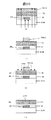
(実施の形態1)
図2に、酸化物半導体を用い作成したトップゲート、ボトムコンタクト型のTFTを示す。ここでいうトップゲートとは、チャネル層CHNよりも上層にゲート電極GEが形成されている構造のことであり、ボトムコンタクトとは、チャネル層CHNよりも下層にソース電極SEおよびドレイン電極DEが形成されている構造のことである。
(Embodiment 1)
FIG. 2 shows a top gate and bottom contact type TFT formed using an oxide semiconductor. The top gate here is a structure in which the gate electrode GE is formed in an upper layer than the channel layer CHN, and the bottom contact is a source electrode SE and a drain electrode DE in the lower layer than the channel layer CHN. It is the structure that is done.
図2(a)は、TFTを上から見た図面である。図2(b)は、図2(a)のA−A´断面を示す図面である。図2(c)は、図2(a)のB−B´断面を示す図面である。 FIG. 2A is a view of the TFT as viewed from above. FIG. 2B is a cross-sectional view taken along the line AA ′ in FIG. FIG.2 (c) is drawing which shows the BB 'cross section of Fig.2 (a).
図2(a)に示すように、半導体装置はソース電極SE、ドレイン電極DE、ゲート電極GE、チャネル層CHNからなる。ソース電極SEは、下層配線LWIへ接続している。ゲート電極GEは、上層配線UWIへ接続している。 As shown in FIG. 2A, the semiconductor device includes a source electrode SE, a drain electrode DE, a gate electrode GE, and a channel layer CHN. The source electrode SE is connected to the lower layer wiring LWI. The gate electrode GE is connected to the upper layer wiring UWI.
図2(b)に示すように、ソース電極SE、ドレイン電極DEは、基板SUB上に形成される。チャネル層CHNは、ソース電極SE、ドレイン電極DEの間、及び、これらの上に形成される。ゲート絶縁膜GIは、ソース電極SE、ドレイン電極DE、チャネル層CHNの上に形成される。ゲート絶縁膜GIの上に、ゲート電極GEが形成される。 As shown in FIG. 2B, the source electrode SE and the drain electrode DE are formed on the substrate SUB. The channel layer CHN is formed between and on the source electrode SE and the drain electrode DE. The gate insulating film GI is formed on the source electrode SE, the drain electrode DE, and the channel layer CHN. A gate electrode GE is formed on the gate insulating film GI.
図2(c)に示すように、下層配線LWIが基板SUB上に形成される。下層配線LWIは、ソース電極SE、ドレイン電極DEと同層である。上層配線UWIは、ゲート絶縁膜GIを介して下層配線LWIより上層に形成される。上層配線UWIは、ゲート電極GEと同層である。 As shown in FIG. 2C, the lower layer wiring LWI is formed on the substrate SUB. The lower layer wiring LWI is in the same layer as the source electrode SE and the drain electrode DE. The upper layer wiring UWI is formed in an upper layer than the lower layer wiring LWI through the gate insulating film GI. The upper layer wiring UWI is in the same layer as the gate electrode GE.
半導体チャネル層CHNを構成する酸化物半導体は金属との間のコンタクト抵抗が小さいため、半導体チャネル層CHNとソース電極SE、ドレイン電極DEを構成する金属膜とを直接接続することができる。このため、シリコン系トランジスタのシリコン−金属間接合において必要となる高濃度不純物層n+、p+は不要である。従い、簡単な構成でTFTを作成できる。 Since the oxide semiconductor constituting the semiconductor channel layer CHN has a low contact resistance with the metal, the semiconductor channel layer CHN and the metal films constituting the source electrode SE and the drain electrode DE can be directly connected. For this reason, the high-concentration impurity layers n + and p + that are necessary in the silicon-metal junction of the silicon-based transistor are unnecessary. Accordingly, a TFT can be created with a simple configuration.
ここで、透明基板SUBは、例えば、ガラス、石英、プラスチックフィルムなどからなり、必要に応じてソース電極SE、ドレイン電極DEが形成される側の表面に絶縁膜のコーティングがなされている。 Here, the transparent substrate SUB is made of, for example, glass, quartz, plastic film, or the like, and an insulating film is coated on the surface on which the source electrode SE and the drain electrode DE are formed as necessary.
ソース電極SE、ドレイン電極DEは、裏面露光に用いる光に対して不透明な材料によって形成されている。たとえば、モリブデン、クロム、タングステン、アルミ、銅、チタン、ニッケル、タンタル、銀、亜鉛、あるいはその他の金属の単膜、それらの合金膜、それらの積層膜、あるいはITO(In−Sn−O:インジウム錫酸化物)などの金属酸化物導電膜と金属との積層膜、窒化チタン(Ti−N)などの金属窒化物導電膜と金属との積層膜、その他の導電性金属化合物膜と金属との積層膜、高濃度にドーピングされた半導体、あるいはドーピングされた半導体と金属との積層膜によって形成されている。 The source electrode SE and the drain electrode DE are formed of a material that is opaque to the light used for backside exposure. For example, molybdenum, chromium, tungsten, aluminum, copper, titanium, nickel, tantalum, silver, zinc, or other metal single films, their alloy films, their laminated films, or ITO (In-Sn-O: Indium A laminated film of a metal oxide conductive film such as tin oxide) and a metal, a laminated film of a metal nitride conductive film such as titanium nitride (Ti-N) and a metal, and other conductive metal compound films and a metal. It is formed of a laminated film, a highly doped semiconductor, or a laminated film of a doped semiconductor and a metal.
ゲート絶縁膜GIは、たとえば、Si−O、Al−Oをはじめとした酸化物を用いるのが好ましいが、Si−Nなど酸化物以外の絶縁膜を用いても良い。 For the gate insulating film GI, for example, an oxide such as Si—O or Al—O is preferably used, but an insulating film other than an oxide such as Si—N may be used.
チャネル層CHNは、たとえば、Zn−O、In-O、Ga-O、Sn-O、In−Ga−Zn−O、Zn−Sn−O、In−Sn−O、In−Zn−O、Ga−Zn−O、In−Ga−Oなどの、Zn、In、Ga、Snの酸化物、およびそれらの複合酸化物によって形成されている。 The channel layer CHN includes, for example, Zn—O, In—O, Ga—O, Sn—O, In—Ga—Zn—O, Zn—Sn—O, In—Sn—O, In—Zn—O, and Ga. It is formed of an oxide of Zn, In, Ga, Sn, such as —Zn—O or In—Ga—O, and a composite oxide thereof.
ゲート電極GEは、たとえば、ITO(In-Sn-O)、Al−Zn-O、Sn−Oなどの透明導電膜、あるいは上記チャネル層CHNに用いた材料の導電性を高めたものによって形成されている。 The gate electrode GE is formed of, for example, a transparent conductive film such as ITO (In—Sn—O), Al—Zn—O, or Sn—O, or a material having increased conductivity of the material used for the channel layer CHN. ing.
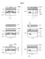
図3A〜図3Bは、図2のTFTの製造工程を示す。(a−1)〜(a−7)は、図2(a)におけるA−A´断面の製造工程である。(b−1)〜(b−7)は、図2(b)におけるB−B´断面の製造工程である。また、(a−1)と(b−1)、(a−2)と(b−2)、(a−3)と(b−3)、(a−4)と(b−4)、(a−5)と(b−5)、(a−6)と(b−6)、(a−7)と(b−7)は同じ製造プロセスを示す。 3A to 3B show a manufacturing process of the TFT of FIG. (A-1) to (a-7) are steps for producing the AA ′ cross section in FIG. (B-1) to (b-7) are manufacturing steps of the BB ′ cross section in FIG. (A-1) and (b-1), (a-2) and (b-2), (a-3) and (b-3), (a-4) and (b-4), (A-5) and (b-5), (a-6) and (b-6), (a-7) and (b-7) show the same manufacturing process.
まず、ステップ(a−1)、(b−1)に示すように、透明基板SUB上に金属によりソース電極SE、ドレイン電極DEが一定距離離間した領域である離間領域を隔てて形成される。また、同プロセスで下層配線LWIが形成される。金属の成膜はCVD法やスパッタ法などにより行ない、ソース電極SE、ドレイン電極DEの形状への加工は一般的なフォトリソグラフィー技術とドライエッチングとの組み合わせにより行なう。 First, as shown in steps (a-1) and (b-1), the source electrode SE and the drain electrode DE are formed on the transparent substrate SUB with a separation region that is a region separated by a certain distance. Further, the lower layer wiring LWI is formed by the same process. The metal film is formed by a CVD method, a sputtering method, or the like, and the processing of the source electrode SE and the drain electrode DE into the shape is performed by a combination of general photolithography technology and dry etching.
なお、透明基板SUB等に用いている透明との語句は、後述する裏面露光の工程において照射される光(水銀ランプのi線 波長365 nmなど)をある程度透過することができるという意味で用いているものであり、必ずしも肉眼で見た時に透明に見えるという意味ではない。 The term “transparent” used for the transparent substrate SUB or the like is used in the sense that it can transmit a certain amount of light (i-line wavelength of the mercury lamp, 365 nm, etc.) irradiated in the back exposure process described later. It does not necessarily mean that it looks transparent when viewed with the naked eye.
続いて、このソース電極SEおよびドレイン電極DEにまたがるように半導体チャネル層CHNが形成される。酸化物半導体の成膜はスパッタ法などにより行ない、チャネル層CHNの形状への加工は一般的なフォトリソグラフィー技術とウェットエッチングあるいはドライエッチングとの組み合わせにより行なう。 Subsequently, a semiconductor channel layer CHN is formed so as to straddle the source electrode SE and the drain electrode DE. The oxide semiconductor film is formed by sputtering or the like, and the processing of the channel layer CHN into a shape is performed by a combination of general photolithography technology and wet etching or dry etching.
そして、ソース電極SE、ドレイン電極DE、半導体チャネル層CHN、下層配線LWIを覆うようにして、ゲート絶縁膜GIが形成される。このゲート絶縁膜GIの成膜はCVD法やスパッタ法などにより行なう。 Then, the gate insulating film GI is formed so as to cover the source electrode SE, the drain electrode DE, the semiconductor channel layer CHN, and the lower layer wiring LWI. The gate insulating film GI is formed by CVD or sputtering.
その後、ゲート絶縁膜GI上にスパッタ法などにより透明導電膜TCLが形成され、さらに、その上にネガレジストNRESが塗布され、透明基板SUBの裏面側よりネガレジストNRESが露光される(裏面露光)。この露光工程においては、金属よりなるソース電極SE、ドレイン電極DEがマスクとして働き、それ以外の部材は露光光を透過するため、ソース電極SE、ドレイン電極DEに対して自己整合的にネガレジストNRESを露光することができる。なお、酸化物半導体は、約250 nmから2000 nm以上の波長の光に対して透過成分を持ち、例えば波長365 nmの光に対しては約75%の透過率を示す。そのため、水銀ランプのi線(波長365 nm)などの短い波長の光により、裏面露光を行うことができる。 Thereafter, a transparent conductive film TCL is formed on the gate insulating film GI by sputtering or the like, and further, a negative resist NRES is applied thereon, and the negative resist NRES is exposed from the back side of the transparent substrate SUB (backside exposure). . In this exposure process, the source electrode SE and drain electrode DE made of metal serve as a mask, and the other members transmit exposure light. Therefore, the negative resist NRES is self-aligned with the source electrode SE and drain electrode DE. Can be exposed. Note that an oxide semiconductor has a transmission component with respect to light with a wavelength of approximately 250 nm to 2000 nm or more, and exhibits a transmittance of approximately 75% with respect to light with a wavelength of 365 nm, for example. Therefore, backside exposure can be performed with light having a short wavelength such as i-line (wavelength 365 nm) of a mercury lamp.
続いて、ステップ(a−2)、(b−2)に示すように、フォトマスクPMを用いて、下層回線LWIと透明導電膜TCLにより形成される上層配線UWIの交差部分上のネガレジストNRESを表面側から露光する。これにより上層配線UWIの分断を防止している。表面側からの露光は、裏面露光の前後に行なえば良いが、裏面露光と同時に行なっても良い。 Subsequently, as shown in steps (a-2) and (b-2), using the photomask PM, the negative resist NRES on the intersection of the upper layer wiring UWI formed by the lower layer line LWI and the transparent conductive film TCL is used. Is exposed from the surface side. This prevents the upper layer wiring UWI from being divided. The exposure from the front side may be performed before and after the back exposure, but may be performed simultaneously with the back exposure.
続いて、ステップ(a−3)、(b−3)に示すように、露光部分以外のネガレジストNRESが除去され、ネガレジストNRESがパターニングされる。 Subsequently, as shown in steps (a-3) and (b-3), the negative resist NRES other than the exposed portion is removed, and the negative resist NRES is patterned.
続いて、ステップ(a−4)、(b−4)に示すように、ネガレジストNRESの露光部分をエッチングマスクとして、透明導電膜TCLをエッチングする。これにより、ゲート電極GEのチャネル方向が形成される。 Subsequently, as shown in steps (a-4) and (b-4), the transparent conductive film TCL is etched using the exposed portion of the negative resist NRES as an etching mask. Thereby, the channel direction of the gate electrode GE is formed.
続いて、ステップ(a−5)、(b−5)に示すように、ネガレジストNRESの露光部分も除去する。 Subsequently, as shown in steps (a-5) and (b-5), the exposed portion of the negative resist NRES is also removed.
続いて、ステップ(a−6)、(b−6)に示すように、透明導電膜TCLから上層配線UWIを形成するため、一般的なフォトリソグラフィー技術とウェットエッチングあるいはドライエッチングとの組み合わせにより透明導電膜TCLをゲート電極GE、上層配線UWIの形状に加工する。ここで(a−6)、(b−6)の図では、ネガレジストNRESを用いた場合を示したが、当然ポジレジストを用いてもよい。その場合、言うまでもなくステップ(a−6)、(b−6)で用いるフォトマスクはネガ/ポジを反転させる。 Subsequently, as shown in steps (a-6) and (b-6), in order to form the upper layer wiring UWI from the transparent conductive film TCL, it is transparent by a combination of general photolithography technology and wet etching or dry etching. The conductive film TCL is processed into the shape of the gate electrode GE and the upper layer wiring UWI. Here, in the diagrams (a-6) and (b-6), the case where the negative resist NRES is used is shown, but a positive resist may naturally be used. In that case, it goes without saying that the photomask used in steps (a-6) and (b-6) inverts the negative / positive.
なお、図3では、ゲート電極GEの加工において、裏面露光を用いた自己整合的な加工であるステップ(a−1)を先に行ない、その後一般的なフォトリソグラフィー技術(a−6)を用いた加工を行なったが、この順序は逆とすることも可能である。 In FIG. 3, in the processing of the gate electrode GE, step (a-1), which is self-aligned processing using backside exposure, is performed first, and then a general photolithography technique (a-6) is used. However, this order can be reversed.
最後に、ステップ(a−7)、(b−7)に示すように、TFT、上層配線LWI、上層配線UWIを得る。 Finally, as shown in steps (a-7) and (b-7), a TFT, an upper layer wiring LWI, and an upper layer wiring UWI are obtained.
以上のプロセスでは、高温プロセスは必要とされないため、プラスチックフィルムなどのフレキシブル基板上に容易にTFTを形成することができる。 In the above process, a high temperature process is not required, so that a TFT can be easily formed on a flexible substrate such as a plastic film.
図4は、図2のTFTのゲート電極周辺を表す図面である。図4(a)は、図3のステップ(a−5)、(b−5)における透明導電膜TCLの形状を示す図面である。図4(b)〜(d)は、図3のステップ(a−6)、(b−6)を経て加工されたゲート電極GEを示す図面である。 FIG. 4 is a view showing the periphery of the gate electrode of the TFT of FIG. FIG. 4A is a diagram showing the shape of the transparent conductive film TCL in steps (a-5) and (b-5) of FIG. 4B to 4D are diagrams showing the gate electrode GE processed through steps (a-6) and (b-6) of FIG.
ステップ(a−6)、(b−6)の加工では自己整合的にレジストを露光することができないため、ゲート電極GEの形状は厳密には、図6(b)に示すような形状とはならず、図6(c)あるいは図6(d)のような凹凸をもった形状となる。 Since the resist cannot be exposed in a self-aligning manner in the processing of steps (a-6) and (b-6), the shape of the gate electrode GE is strictly the shape as shown in FIG. Instead, it has a shape with irregularities as shown in FIG. 6C or FIG.
図5は、図3のステップ(a−1)において金属のエッチングをウェットエッチングにより行い、ソース電極SE、ドレイン電極DEを形成したTFTを示す図面である。図2ではソース電極SE、ドレイン電極DEの形成にドライエッチングを用いた場合の例を示したため、ソース電極SEの離間領域側の端部およびドレイン電極DEの離間領域側の端部が実質上垂直形状をしている。ウェットエッチングを用いた場合には、ソース電極SEの離間領域側の端部およびドレイン電極DEの離間領域側の端部は、先端部に行くにつれて高さが低くなるテーパ形状となる。 FIG. 5 is a drawing showing a TFT in which the metal is etched by wet etching in step (a-1) of FIG. 3 to form the source electrode SE and the drain electrode DE. Since FIG. 2 shows an example in which dry etching is used to form the source electrode SE and the drain electrode DE, the end of the source electrode SE on the separated region side and the end of the drain electrode DE on the separated region side are substantially vertical. It has a shape. When wet etching is used, the end of the source electrode SE on the side of the separation region and the end of the drain electrode DE on the side of the separation region are tapered so that the height decreases toward the tip.
ドライエッチングを用いた場合、加工精度高まるというメリットがあり、ウェットエッチングを用いた場合、チャネル層CHNを形成する際にソース電極SEおよびドレイン電極DEに対する被覆性が高まるというメリットがある。 When dry etching is used, there is a merit that processing accuracy is increased, and when wet etching is used, there is an advantage that coverage with respect to the source electrode SE and the drain electrode DE is increased when the channel layer CHN is formed.
図6に、酸化物半導体を用い作成したトップゲート、ボトムコンタクト型のTFTを示す。図6(a)は、TFTを上から見た図面である。図6(b)は、図2(a)のA−A´断面を示す図面である。図6(c)は、図6(a)のB−B´断面を示す図面である。図6は、透明導電膜TCLの上に、導電層CLが形成されている点で図2と異なる。図6の構造では、上層配線UWIが、透明導電膜TCL、導電層CLの2層構造となるため、上層配線の導電性が増す。 FIG. 6 shows a top gate and bottom contact TFT formed using an oxide semiconductor. FIG. 6A shows the TFT as viewed from above. FIG. 6B is a cross-sectional view taken along the line AA ′ of FIG. FIG.6 (c) is drawing which shows the BB 'cross section of Fig.6 (a). FIG. 6 differs from FIG. 2 in that a conductive layer CL is formed on the transparent conductive film TCL. In the structure of FIG. 6, since the upper layer wiring UWI has a two-layer structure of the transparent conductive film TCL and the conductive layer CL, the conductivity of the upper layer wiring is increased.
図6(a)は、透明導電膜TCLの上に導電層CLが形成されている他は、図2(a)と同様なので、説明を省略する。図6(b)は、図2(b)と同様なので説明を省略する。 FIG. 6A is the same as FIG. 2A except that the conductive layer CL is formed on the transparent conductive film TCL, and a description thereof will be omitted. Since FIG. 6B is the same as FIG.
図6(c)に示すように、下層配線LWIが基板SUB上に形成される。下層配線LWIは、ソース電極SE、ドレイン電極DEと同層である。上層配線UWIは、ゲート絶縁膜GIを介して下層配線LWIより上層に形成される。上層配線UWIは、ゲート電極GEと同層である。 As shown in FIG. 6C, the lower layer wiring LWI is formed on the substrate SUB. The lower layer wiring LWI is in the same layer as the source electrode SE and the drain electrode DE. The upper layer wiring UWI is formed in an upper layer than the lower layer wiring LWI through the gate insulating film GI. The upper layer wiring UWI is in the same layer as the gate electrode GE.
図7A〜図7Cは、図6のTFTの製造工程を示す。(a−1)〜(a−7)は、図6(a)におけるA−A´断面の製造工程である。(b−1)〜(b−7)は、図6(b)におけるB−B´断面の製造工程である。また、(a−1)と(b−1)、(a−2)と(b−2)、(a−3)と(b−3)、(a−4)と(b−4)、(a−5)と(b−5)、(a−6)と(b−6)、(a−7)と(b−7)、(a−8)と(b−8)、(a−9)と(b−9)、(a−10)と(b−10)、(a−11)と(b−11)は同じ製造プロセスを示す。 7A to 7C show a manufacturing process of the TFT of FIG. (A-1) to (a-7) are manufacturing steps of the AA ′ cross section in FIG. (B-1) to (b-7) are manufacturing steps of the BB ′ cross section in FIG. (A-1) and (b-1), (a-2) and (b-2), (a-3) and (b-3), (a-4) and (b-4), (A-5) and (b-5), (a-6) and (b-6), (a-7) and (b-7), (a-8) and (b-8), (a -9) and (b-9), (a-10) and (b-10), (a-11) and (b-11) show the same manufacturing process.
図7のステップ(a−1)、(b−1)は、図3のステップ(a−1)、(b−1)と同様なので説明を省略する。 Steps (a-1) and (b-1) in FIG. 7 are the same as steps (a-1) and (b-1) in FIG.
ステップ(a−1)、(b−1)に続いて、ステップ(a−2)、(b−2)に示すように、露光部分以外のネガレジストNRESが除去され、ネガレジストNRESがパターニングされる。 Subsequent to steps (a-1) and (b-1), as shown in steps (a-2) and (b-2), the negative resist NRES other than the exposed portion is removed, and the negative resist NRES is patterned. The
続いて、ステップ(a−3)、(b−3)に示すように、ネガレジストNRESの露光部分をエッチングマスクとして、透明導電膜TCLをエッチングする。これにより、ゲート電極GEのチャネル方向が形成される。 Subsequently, as shown in steps (a-3) and (b-3), the transparent conductive film TCL is etched using the exposed portion of the negative resist NRES as an etching mask. Thereby, the channel direction of the gate electrode GE is formed.
続いて、ステップ(a−4)、(b−4)に示すように、ネガレジストNRESの露光部分も除去する。 Subsequently, as shown in steps (a-4) and (b-4), the exposed portion of the negative resist NRES is also removed.
続いて、ステップ(a−5)、(b−5)に示すように、透明導電膜TCLから上層配線UWIを形成するため、一般的なフォトリソグラフィー技術とウェットエッチングあるいはドライエッチングとの組み合わせにより透明導電膜TCLをゲート電極GE、上層配線UWIの形状に加工する。ここで(a−6)、(b−6)の図では、ネガレジストNRESを用いた場合を示したが、当然ポジレジストを用いてもよい。その場合、言うまでもなくステップ(a−6)、(b−6)で用いるフォトマスクはネガ/ポジを反転させる。 Subsequently, as shown in steps (a-5) and (b-5), in order to form the upper layer wiring UWI from the transparent conductive film TCL, it is transparent by a combination of general photolithography technology and wet etching or dry etching. The conductive film TCL is processed into the shape of the gate electrode GE and the upper layer wiring UWI. Here, in the diagrams (a-6) and (b-6), the case where the negative resist NRES is used is shown, but a positive resist may naturally be used. In that case, it goes without saying that the photomask used in steps (a-6) and (b-6) inverts the negative / positive.
続いて、ステップ(a−6)、(b−6)に示すような構造を得る。 Subsequently, a structure as shown in steps (a-6) and (b-6) is obtained.
続いて、ステップ(a−7)、(b−7)に示すように、ゲート絶縁膜GI、ゲート電極GE、透明導電膜TCLから成る上層配線UWIの上に、透明導電膜TCLから成る上層配線UWIの間隙領域を埋めるため
導電層CLを形成する。導電層CLの成膜はCVD法やスパッタ法などにより行ない、加工は一般的なフォトリソグラフィー技術とドライエッチングとの組み合わせにより行なう。
Subsequently, as shown in steps (a-7) and (b-7), the upper layer wiring made of the transparent conductive film TCL is formed on the upper layer wiring UWI made of the gate insulating film GI, the gate electrode GE, and the transparent conductive film TCL. A conductive layer CL is formed to fill the gap region of the UWI. The conductive layer CL is formed by a CVD method or a sputtering method, and the processing is performed by a combination of a general photolithography technique and dry etching.
続いて、ステップ(a−8)、(b−8)に示すように、導電層CLの上に、ネガレジストNRESを塗布する。そして、フォトマスクPMを用いて、透明導電層TCLからなる上層配線UWI上のネガレジストNRES、及び、下層回線LWIと透明導電膜TCLにより形成される上層配線UWIの交差部分上を表面側から露光する。なお、導電層CLを形成する目的は、透明導電膜TCLの間隙領域を埋めるためであるので、最低限、下層回線LWIと透明導電膜TCLにより形成される上層配線UWIの交差部分上を表面側から露光できれば良い。 Subsequently, as shown in steps (a-8) and (b-8), a negative resist NRES is applied on the conductive layer CL. Then, using the photomask PM, the negative resist NRES on the upper layer wiring UWI made of the transparent conductive layer TCL and the intersection of the upper layer wiring UWI formed by the lower layer line LWI and the transparent conductive film TCL are exposed from the surface side. To do. Since the purpose of forming the conductive layer CL is to fill the gap region of the transparent conductive film TCL, at least the surface of the intersection portion of the upper layer wiring UWI formed by the lower layer line LWI and the transparent conductive film TCL is on the surface side. It is sufficient if exposure can be performed from
続いて、ステップ(a−9)、(b−9)に示すように、露光部分以外のネガレジストNRESが除去され、ネガレジストNRESがパターニングされる。 Subsequently, as shown in steps (a-9) and (b-9), the negative resist NRES other than the exposed portion is removed, and the negative resist NRES is patterned.
続いて、ステップ(a−10)、(b−10)に示すように、ネガレジストNRESの露光部分をエッチングマスクとして、導電層CLをエッチングする。これにより、上層配線UWIは、透明導電膜TCL、導電層CLの2層となる。ここで(a−8)、(b−8)、(a−9)、(b−9)、(a−10)、(b−10)の図では、ネガレジストNRESを用いた場合を示したが、当然ポジレジストを用いてもよい。その場合、言うまでもなくステップ(a−8)、(b−8)で用いるフォトマスクはネガ/ポジを反転させる。 Subsequently, as shown in steps (a-10) and (b-10), the conductive layer CL is etched using the exposed portion of the negative resist NRES as an etching mask. Thereby, the upper layer wiring UWI becomes two layers of the transparent conductive film TCL and the conductive layer CL. Here, in the diagrams (a-8), (b-8), (a-9), (b-9), (a-10), and (b-10), the case where the negative resist NRES is used is shown. Of course, a positive resist may be used. In that case, it goes without saying that the photomask used in steps (a-8) and (b-8) inverts the negative / positive.
続いて、ネガレジストNRESの露光部分も除去し、ステップ(a−11)、(b−11)に示す構造を得る。 Subsequently, the exposed portion of the negative resist NRES is also removed to obtain the structure shown in steps (a-11) and (b-11).
以上のプロセスでは、高温プロセスは必要とされないため、プラスチックフィルムなどのフレキシブル基板上に容易にTFTを形成することができる。 In the above process, a high temperature process is not required, so that a TFT can be easily formed on a flexible substrate such as a plastic film.
ステップ(b−1)における裏面からの露光光が下層配線LWIにより遮断されるため、下層配線LWIと上層配線UWIの交差部分は露光されず、交差部分上のネガレジストNRESが除去される。交差部分の透明導電膜TCLからなる上層配線UWIがエッチングにより分断され、間隙領域が生じてしまう。図7に示す製造工程によれば、この間隙領域を導電層CLにより埋め、分断された透明導電膜から成る上層配線UWIを短絡させることができる。加えて、上層配線UWIが、透明導電膜TCL、導電層CLの2層構造となるため、上層配線の導電性が増す。 Since the exposure light from the back surface in step (b-1) is blocked by the lower layer wiring LWI, the intersection of the lower layer wiring LWI and the upper layer wiring UWI is not exposed, and the negative resist NRES on the intersection is removed. The upper layer wiring UWI made of the transparent conductive film TCL at the intersecting portion is divided by etching, and a gap region is generated. According to the manufacturing process shown in FIG. 7, the gap region is filled with the conductive layer CL, and the upper wiring UWI made of the divided transparent conductive film can be short-circuited. In addition, since the upper layer wiring UWI has a two-layer structure of the transparent conductive film TCL and the conductive layer CL, the conductivity of the upper layer wiring is increased.
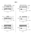
図8に、酸化物半導体を用い作成したトップゲート、ボトムコンタクト型のTFTを示す。図8(a)は、TFTを上から見た図面である。図8(b)は、図2(a)のA−A´断面を示す図面である。図8(c)は、図8(a)のB−B´断面を示す図面である。図8は、上層配線UWIを2層配線とせず、透明導電膜TCLの間隙領域のみを導電層CLにより埋めている点が、図6とは異なる。 FIG. 8 shows a top-gate and bottom-contact TFT manufactured using an oxide semiconductor. FIG. 8A shows the TFT as viewed from above. FIG.8 (b) is drawing which shows the AA 'cross section of Fig.2 (a). FIG.8 (c) is drawing which shows the BB 'cross section of Fig.8 (a). FIG. 8 differs from FIG. 6 in that the upper layer wiring UWI is not a two-layer wiring and only the gap region of the transparent conductive film TCL is filled with the conductive layer CL.
図9に、酸化物半導体を用い作成したトップゲート、ボトムコンタクト型のTFTを示す。図8(a)は、TFTを上から見た図面である。図8(b)は、図2(a)のA−A´断面を示す図面である。図8(c)は、図8(a)のB−B´断面を示す図面である。図9は、ゲート電極GEが、透明導電膜TCLと導電層CLの2層構造となっている点において、図6とは異なる。 FIG. 9 shows a top gate and bottom contact TFT formed using an oxide semiconductor. FIG. 8A shows the TFT as viewed from above. FIG.8 (b) is drawing which shows the AA 'cross section of Fig.2 (a). FIG.8 (c) is drawing which shows the BB 'cross section of Fig.8 (a). 9 differs from FIG. 6 in that the gate electrode GE has a two-layer structure of a transparent conductive film TCL and a conductive layer CL.
図10は、本実施の形態におけるTFTを2層積層した半導体装置を示す図である。図10の半導体装置は、上述した製造方法に従い図2(a)、図6(a)のTFTを製造したのち、TFTを絶縁膜IFで覆い、その上に再びTFTを製造したものである。第2層目のTFTの製造においても、最初に金属で形成したソース電極SE、ドレイン電極DEをマスクに用い、裏面露光を適用することで自己整合的にソース電極SE2、ドレイン電極DE2、ゲート電極GE2を形成する。なお、図10でもTFT部に上述したトップゲート/ボトムコンタクト型のTFTを用いた場合の例を示したが、実施の形態2で示すトップゲート/トップコンタクト型のTFTを用いても良い。
FIG. 10 shows a semiconductor device in which two layers of TFTs in this embodiment are stacked. The semiconductor device of FIG. 10 is obtained by manufacturing the TFT of FIGS. 2A and 6A according to the manufacturing method described above, and then covering the TFT with the insulating film IF and manufacturing the TFT again thereon. Also in the manufacture of the second layer TFT, the source electrode SE, drain electrode DE2, and gate electrode are formed in a self-aligned manner by applying back exposure using the source electrode SE and drain electrode DE initially formed of metal as a mask. GE2 is formed. Although FIG. 10 shows an example in which the above-described top gate / bottom contact type TFT is used for the TFT portion, the top gate / top contact type TFT shown in
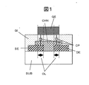
以上、本実施の形態1における自己整合型酸化物TFTによれば、図1に示すような、表面露光のみを用いて形成した際に生じていた、ソース電極SEおよびドレイン電極DEとゲート電極GEとの間のオーバラップOL、ならびにこのオーバラップOLに起因して生じていた寄生容量CPの発生を抑制することができる。また、ソース電極SE、ドレイン電極DEに金属を用いるため、これらの電極、あるいはこれらの電極と一括に形成した配線の抵抗が十分に低い半導体装置を提供することができる。 As described above, according to the self-aligned oxide TFT according to the first embodiment, the source electrode SE, the drain electrode DE, and the gate electrode GE that are generated when only surface exposure is performed as shown in FIG. And the occurrence of the parasitic capacitance CP caused by the overlap OL can be suppressed. In addition, since metal is used for the source electrode SE and the drain electrode DE, a semiconductor device in which the resistance of these electrodes or wirings formed together with these electrodes is sufficiently low can be provided.
(実施の形態2)
図11は、本実施の形態2における半導体装置の構成および製造方法を示す図である。半導体装置としていわゆるトップゲート/トップコンタクト型酸化物TFTを挙げている。ここでいうトップゲートとは、チャネル層CHNよりも上層にゲート電極GEが形成されている構造のことであり、トップコンタクトとは、チャネル層CHNよりも上層にソース電極SEおよびドレイン電極DEが形成されている構造のことを示している。
(Embodiment 2)
FIG. 11 is a diagram illustrating a configuration of a semiconductor device and a manufacturing method according to the second embodiment. A so-called top gate / top contact type oxide TFT is cited as a semiconductor device. The top gate here is a structure in which the gate electrode GE is formed above the channel layer CHN, and the top contact is the source electrode SE and drain electrode DE formed above the channel layer CHN. The structure is shown.
本実施の形態2における半導体装置の製造方法は以下の通りである(各工程の詳細は実施の形態1に準ずる)。まず、図11(a)に示すように、透明基板SUB上に半導体チャネル層CHNが形成される。続いて、この半導体チャネル層CHN上に、金属によりソース電極SE、ドレイン電極DEが形成される。ソース電極SE、ドレイン電極DEは一定距離離間した領域である離間領域を隔てて形成されており、この離間領域は半導体チャネル層CHNの直上にある。そして、半導体チャネル層CHN、ソース電極SE、ドレイン電極DEを覆うようにして、ゲート絶縁膜GIが形成される。その後、ゲート絶縁膜GI上に透明導電膜TCLが形成され、さらにその上にネガレジストNRESが塗布され、透明基板SUBの裏面側よりネガレジストNRESが露光される(裏面露光)。この露光工程においては、金属よりなるソース電極SE、ドレイン電極DEがマスクとして働き、それ以外の部材は露光光を透過するため、ソース電極SE、ドレイン電極DEに対して自己整合的にネガレジストNRESを露光することができる。続いて、ネガレジストNRESが図11(b)に示すようにパターニングされ、透明導電膜TCLが図11(c)に示すようにゲート電極GEの形状に加工される。続いて、ネガレジストNRESを除去し、図11(d)に示すような構造を得る。最後に、実施の形態1の図6で行なった加工と同様に、一般的なフォトリソグラフィー技術とウェットエッチングあるいはドライエッチングとの組み合わせにより透明導電膜TCLをゲート電極GEの形状に加工し、TFT構造を得る。 The manufacturing method of the semiconductor device in the second embodiment is as follows (the details of each step are the same as those in the first embodiment). First, as shown in FIG. 11A, the semiconductor channel layer CHN is formed on the transparent substrate SUB. Subsequently, a source electrode SE and a drain electrode DE are formed on the semiconductor channel layer CHN with a metal. The source electrode SE and the drain electrode DE are formed with a separation region which is a region separated by a certain distance, and this separation region is immediately above the semiconductor channel layer CHN. Then, the gate insulating film GI is formed so as to cover the semiconductor channel layer CHN, the source electrode SE, and the drain electrode DE. Thereafter, a transparent conductive film TCL is formed on the gate insulating film GI, a negative resist NRES is further applied thereon, and the negative resist NRES is exposed from the back side of the transparent substrate SUB (backside exposure). In this exposure process, the source electrode SE and drain electrode DE made of metal serve as a mask, and the other members transmit exposure light. Therefore, the negative resist NRES is self-aligned with the source electrode SE and drain electrode DE. Can be exposed. Subsequently, the negative resist NRES is patterned as shown in FIG. 11B, and the transparent conductive film TCL is processed into the shape of the gate electrode GE as shown in FIG. Subsequently, the negative resist NRES is removed to obtain a structure as shown in FIG. Finally, similar to the processing performed in FIG. 6 of the first embodiment, the transparent conductive film TCL is processed into the shape of the gate electrode GE by a combination of general photolithography technology and wet etching or dry etching, and the TFT structure Get.
なお、上述の説明ではゲート電極GEの加工において、裏面露光を用いた自己整合的な加工を先に行ない、その後一般的なフォトリソグラフィー技術を用いた加工を行なったが、この順序は逆とすることも可能である。 In the above description, in the processing of the gate electrode GE, self-aligned processing using backside exposure is performed first, and then processing using a general photolithography technique is performed, but this order is reversed. It is also possible.
図11ではソース電極SE、ドレイン電極DEの形成にドライエッチングを用いた場合の例を示したため、ソース電極SEの離間領域側の端部およびドレイン電極DEの離間領域側の端部が、実質上垂直形状をしているが、実施の形態1で示したのと同様にドライエッチング代わりにウェットエッチングを用いても良い。その場合、ソース電極SEの離間領域側の端部およびドレイン電極DEの離間領域側の端部は、先端部に行くにつれて高さが低くなるテーパ形状となる。ドライエッチングを用いた場合、加工精度が高まるというメリットがありと、ウェットエッチングを用いた場合、チャネル層CHNに与えるダメージが小さいというメリットがある。 FIG. 11 shows an example in which dry etching is used to form the source electrode SE and the drain electrode DE. Therefore, the end of the source electrode SE on the side of the separation region and the end of the drain electrode DE on the side of the separation region are substantially Although it has a vertical shape, wet etching may be used instead of dry etching as in the first embodiment. In that case, the end of the source electrode SE on the side of the separation region and the end of the drain electrode DE on the side of the separation region have a tapered shape whose height decreases toward the tip. When dry etching is used, there is an advantage that the processing accuracy is increased, and when wet etching is used, there is an advantage that damage to the channel layer CHN is small.
本実施の形態2における各部材は実施の形態1に示したのと同様の材料によって形成されている。 Each member in the second embodiment is formed of the same material as that shown in the first embodiment.
以上、本実施の形態2における自己整合型酸化物TFTによれば、図1に示すような、表面露光のみを用いて形成した際に生じていたソース電極SEおよびドレイン電極DEとゲート電極GEとの間のオーバラップOL、ならびにこのオーバラップOLに起因して生じていた寄生容量CPの発生を抑制することができる。また、ソース電極SE、ドレイン電極DEに金属を用いるため、これらの電極、あるいはこれらの電極と一括に形成した配線の抵抗が十分に低い半導体装置を提供することができる。 As described above, according to the self-aligned oxide TFT according to the second embodiment, the source electrode SE, the drain electrode DE, and the gate electrode GE that are generated when only surface exposure is performed as shown in FIG. And the generation of the parasitic capacitance CP caused by the overlap OL can be suppressed. In addition, since metal is used for the source electrode SE and the drain electrode DE, a semiconductor device in which the resistance of these electrodes or wirings formed together with these electrodes is sufficiently low can be provided.
(実施の形態3)
図12は、本実施の形態3における半導体装置の構成および製造方法を示す図である。半導体装置としていわゆるボトムゲート/トップコンタクト型酸化物TFTを挙げている。ここでいうボトムゲートとは、チャネル層CHNよりも下層にゲート電極GEが形成されている構造のことであり、トップコンタクトとは、チャネル層CHNよりも上層にソース電極SEおよびドレイン電極DEが形成されている構造のことを示している。
(Embodiment 3)
FIG. 12 is a diagram showing the configuration of the semiconductor device and the manufacturing method according to the third embodiment. A so-called bottom gate / top contact type oxide TFT is cited as a semiconductor device. The bottom gate here is a structure in which the gate electrode GE is formed below the channel layer CHN, and the top contact is the source electrode SE and drain electrode DE formed above the channel layer CHN. The structure is shown.
本実施の形態3における半導体装置の製造方法は以下の通りである。まず、図12(a)に示すように、透明基板SUB上に金属によりゲート電極GE形成される。金属の成膜はCVD法やスパッタ法などにより行ない、ゲート電極GEの形状への加工は一般的なフォトリソグラフィー技術とドライエッチングあるいはウェットエッチングとの組み合わせにより行なう。 The manufacturing method of the semiconductor device according to the third embodiment is as follows. First, as shown in FIG. 12A, the gate electrode GE is formed of metal on the transparent substrate SUB. The metal film is formed by a CVD method, a sputtering method, or the like, and the gate electrode GE is processed into a shape by a combination of a general photolithography technique and dry etching or wet etching.
続いて、このゲート電極GEを覆うようにして、ゲート絶縁膜GIが形成される。このゲート絶縁膜GIの成膜はCVD法やスパッタ法などにより行なう。 Subsequently, a gate insulating film GI is formed so as to cover the gate electrode GE. The gate insulating film GI is formed by CVD or sputtering.
そして、ゲート絶縁膜GI上にゲート電極GEを覆うようにして半導体チャネル層CHNが形成される。酸化物半導体の成膜はスパッタ法などにより行ない、チャネル層CHNの形状への加工は一般的なフォトリソグラフィー技術とウェットエッチングあるいはドライエッチングとの組み合わせにより行なう。 Then, the semiconductor channel layer CHN is formed on the gate insulating film GI so as to cover the gate electrode GE. The oxide semiconductor film is formed by sputtering or the like, and the processing of the channel layer CHN into a shape is performed by a combination of general photolithography technology and wet etching or dry etching.
その後、チャネル層CHNを覆うようにしてスパッタ法などにより透明導電膜TCLが形成され、さらに、その上にネガレジストNRESが塗布され、透明基板SUBの裏面側よりネガレジストNRESが露光される(裏面露光)。この露光工程においては、金属よりなるゲート電極GEがマスクとして働き、それ以外の部材は露光光を透過するため、ゲート電極GEに対して自己整合的にネガレジストNRESを露光することができる。 Thereafter, a transparent conductive film TCL is formed by sputtering or the like so as to cover the channel layer CHN, and further, a negative resist NRES is applied thereon, and the negative resist NRES is exposed from the back side of the transparent substrate SUB (back side) exposure). In this exposure process, the gate electrode GE made of metal serves as a mask and the other members transmit the exposure light, so that the negative resist NRES can be exposed in a self-aligned manner with respect to the gate electrode GE.
続いて、ネガレジストNRESが図12(b)に示すようにパターニングされ、透明導電膜TCLが図12(c)に示すように加工される。その後、ネガレジストNRESを除去し、図12(d)(断面図)、図13(a)(上面から見た平面図。A−A’の断面が図12(d)に当たる)に示すような構造を得る。最後に、一般的なフォトリソグラフィー技術とウェットエッチングあるいはドライエッチングとの組み合わせにより透明導電膜TCLをソース電極SEおよびドレイン電極DEの形状に加工し、図13(b)に示すようなTFT構造を得る。 Subsequently, the negative resist NRES is patterned as shown in FIG. 12B, and the transparent conductive film TCL is processed as shown in FIG. Thereafter, the negative resist NRES is removed, and as shown in FIG. 12D (cross-sectional view) and FIG. 13A (a plan view seen from above, the cross section AA ′ corresponds to FIG. 12D). Get the structure. Finally, the transparent conductive film TCL is processed into the shape of the source electrode SE and the drain electrode DE by a combination of general photolithography technology and wet etching or dry etching to obtain a TFT structure as shown in FIG. .
なお、上述の説明ではソース電極SEおよびドレイン電極DEの加工において、裏面露光を用いた自己整合的な加工を先に行ない、その後一般的なフォトリソグラフィー技術を用いた加工を行なったが、この順序は逆とすることも可能である。 In the above description, in the processing of the source electrode SE and the drain electrode DE, self-aligned processing using backside exposure is performed first, and then processing using a general photolithography technique is performed. Can be reversed.
本実施の形態3における各部材は基本的には実施の形態1に示したのと同様の材料によって形成されている。ただし、上述の製造方法を読めばわかる通り、ゲート電極GEには実施の形態1のソース電極SE、ドレイン電極DEに用いた材料を用い、ソース電極SE、ドレイン電極DEには実施の形態1のゲート電極GEに用いた材料を用いる。
Each member in the third embodiment is basically formed of the same material as that shown in the first embodiment. However, as can be seen from the above manufacturing method, the material used for the source electrode SE and drain electrode DE of
本実施の形態によれば、チャネル層CHNを酸化物半導体を用いて作製しているため、水銀ランプのi線(波長365 nm)などの短い波長の光により、裏面露光を行うことができる。加えて、半導体チャネル層CHNを構成する酸化物半導体は多くの金属との間のコンタクト抵抗が小さいため、半導体チャネル層CHNとソース電極SE、ドレイン電極DEを構成する金属膜とを直接接続することができる。 According to this embodiment, since the channel layer CHN is manufactured using an oxide semiconductor, the back surface exposure can be performed with light having a short wavelength such as i-line (wavelength 365 nm) of a mercury lamp. In addition, since the oxide semiconductor constituting the semiconductor channel layer CHN has a small contact resistance with many metals, the semiconductor channel layer CHN and the metal films constituting the source electrode SE and the drain electrode DE are directly connected. Can do.
図12ではソース電極SE、ドレイン電極DEの形成にドライエッチングを用いた場合の例を示したため、ソース電極SEの離間領域側の端部およびドレイン電極DEの離間領域側の端部が、実質上垂直形状をしているが、実施の形態1で示したのと同様にドライエッチング代わりにウェットエッチングを用いても良い。その場合、ソース電極SEの離間領域側の端部およびドレイン電極DEの離間領域側の端部は、先端部に行くにつれて高さが低くなるテーパ形状となる。ドライエッチングを用いた場合、加工精度高まるというメリットがありと、ウェットエッチングを用いた場合、チャネル層CHNに与えるダメージが小さいというメリットがある。 FIG. 12 shows an example in which dry etching is used to form the source electrode SE and the drain electrode DE. Therefore, the end of the source electrode SE on the side of the separation region and the end of the drain electrode DE on the side of the separation region are substantially Although it has a vertical shape, wet etching may be used instead of dry etching as in the first embodiment. In that case, the end of the source electrode SE on the side of the separation region and the end of the drain electrode DE on the side of the separation region have a tapered shape whose height decreases toward the tip. When dry etching is used, there is a merit that processing accuracy is increased, and when wet etching is used, there is an advantage that damage to the channel layer CHN is small.
図12の製造方法に従い、ゲート電極GEと同工程により下層配線LWIと形成し、ソース電極SE、ドレイン電極DEと同工程により上層配線UWIを形成する場合を考える。裏面からの露光光が下層配線LWIにより遮断されるため、下層配線LWIと上層配線UWIの交差部分は露光されず、交差部分上のネガレジストNRESが除去される結果、交差部分の上層配線UWIがエッチングにより分断され、間隙領域が生じてしまう。このため、間隙領域を埋め、分断された上層配線UWIを短絡させる必要がある。 Consider the case where the lower layer wiring LWI is formed by the same process as the gate electrode GE and the upper layer wiring UWI is formed by the same process as the source electrode SE and drain electrode DE in accordance with the manufacturing method of FIG. Since the exposure light from the back surface is blocked by the lower layer wiring LWI, the intersection part of the lower layer wiring LWI and the upper layer wiring UWI is not exposed, and the negative resist NRES on the intersection part is removed. It is divided by etching, and a gap region is generated. For this reason, it is necessary to fill the gap region and to short-circuit the divided upper layer wiring UWI.
図13は、図12のTFTのゲート電極周辺を表す図面である。図13(a)は、図12のステップ(d)における透明導電膜TCLの形状を示す図面である。図13(b)は、透明導電膜TCLを加工し、ソース電極、ドレイン電極を形成したTFTのゲート電極周辺を表す図面である。 FIG. 13 is a view showing the periphery of the gate electrode of the TFT of FIG. FIG. 13A is a drawing showing the shape of the transparent conductive film TCL in step (d) of FIG. FIG. 13B is a diagram showing the periphery of the gate electrode of the TFT in which the transparent conductive film TCL is processed to form the source electrode and the drain electrode.
図14では、金属あるいは金属酸化物などの導電層CLにより間隙領域を埋め、分断された上層配線UWIを短絡させる方法について説明する。 FIG. 14 illustrates a method for short-circuiting the separated upper layer wiring UWI by filling the gap region with a conductive layer CL such as metal or metal oxide.
図14は、図12において、ゲート電極GEと下層配線LWIを一体に形成し、ソース電極SEと上層配線UWIを一体に形成した場合の半導体装置を示す図である。図14(a)のA−A’の断面が図12に当たる。また、B−B’の断面が図14(b)にあたる。 FIG. 14 is a diagram showing a semiconductor device when the gate electrode GE and the lower layer wiring LWI are integrally formed and the source electrode SE and the upper layer wiring UWI are integrally formed in FIG. FIG. 12 is a cross-sectional view taken along A-A ′ in FIG. Further, a cross section taken along line B-B 'corresponds to FIG.
図14において、下層配線LWIは、図12におけるゲート電極GEと同一工程により加工・形成される。すなわち、下層配線LWIの成膜はCVD法やスパッタ法などにより行ない、加工は一般的なフォトリソグラフィー技術とドライエッチングとの組み合わせにより行なう。 In FIG. 14, the lower layer wiring LWI is processed and formed in the same process as the gate electrode GE in FIG. That is, the lower layer wiring LWI is formed by a CVD method or a sputtering method, and the processing is performed by a combination of a general photolithography technique and dry etching.
下層配線LWIと上層配線UWIを隔てるゲート絶縁膜層GIは、図12のゲート絶縁膜と同一工程により形成される。すなわち、ゲート絶縁膜GIの成膜はCVD法やスパッタ法などにより行なう。 The gate insulating film layer GI separating the lower layer wiring LWI and the upper layer wiring UWI is formed by the same process as the gate insulating film of FIG. That is, the gate insulating film GI is formed by a CVD method or a sputtering method.
上層配線UWIを構成する透明導電膜TCLは、図12におけるソース電極SE、ドレイン電極DEと同一工程により加工・形成される。すなわち、上層配線UWIの成膜はスパッタ法などにより行ない、加工は裏面露光を用いた自己整合的な加工と一般的なフォトリソグラフィー技術を用いた加工の2回に分けて行なう。上層配線UWIを構成する導電膜CLは、成膜をスパッタ法などにより行ない、加工を一般的なフォトリソグラフィー技術とウェットエッチングあるいはドライエッチングとの組み合わせにより行なう。 The transparent conductive film TCL constituting the upper layer wiring UWI is processed and formed in the same process as the source electrode SE and the drain electrode DE in FIG. That is, the upper layer wiring UWI is formed by sputtering or the like, and the processing is performed in two steps, that is, self-aligned processing using backside exposure and processing using a general photolithography technique. The conductive film CL constituting the upper layer wiring UWI is formed by sputtering or the like and processed by a combination of general photolithography technology and wet etching or dry etching.
なお、図14(a)と同様の工程により、図14(c)に示すように下層配線LWI、上層配線UWIとの交差部分のみについて、導電層CLを作製することもできる。また、同様に、図14(d)に示すように、上層配線UWIの部分のみならず、ソース電極SE、ドレイン電極DE上にも導電層CLを作製することも可能である。 Note that the conductive layer CL can be formed only in the intersection with the lower layer wiring LWI and the upper layer wiring UWI as shown in FIG. 14C by the same process as in FIG. Similarly, as shown in FIG. 14D, the conductive layer CL can be formed not only on the upper layer wiring UWI but also on the source electrode SE and the drain electrode DE.
また、図14ではTFT部に上述したボトムゲート/トップコンタクト型のTFTを用いた場合の例を示したが、実施の形態4で示すボトムゲート/ボトムコンタクト型のTFTを用いても良い。
14 shows an example in which the above-described bottom gate / top contact type TFT is used in the TFT portion, the bottom gate / bottom contact type TFT shown in
図15は、本実施の形態において、ゲート電極GEと下層配線LWIを一体に形成し、ソース電極SEと上層配線UWIを別の方法で一体に形成した場合の半導体装置を示す図である。図15(a)のA−A’の断面が図12に当たる。また、B−B’の断面が図15(b)にあたる。 FIG. 15 is a diagram showing a semiconductor device when the gate electrode GE and the lower layer wiring LWI are integrally formed and the source electrode SE and the upper layer wiring UWI are integrally formed by another method in the present embodiment. FIG. 12 is a cross-sectional view taken along line A-A ′ of FIG. Further, the cross section of B-B ′ corresponds to FIG.
図15と図14の違いは、ネガレジストNRESの露光の方法のみであるので、ネガレジストNRES塗布前の工程の説明は図14の説明により代替する。 Since the difference between FIG. 15 and FIG. 14 is only the method of exposing the negative resist NRES, the description of the process before applying the negative resist NRES is replaced by the description of FIG.
図15の構造では、通常のフォトマスクPMを用いて、選択的に交差部分上のネガレジストNRESを表面側から露光する。これにより上層配線UWIの分断を防止している。表面側からの露光は、裏面露光の前後に行なえば良いが、裏面露光と同時に行なっても良い。なお、図15でもTFT部に上述したボトムゲート/トップコンタクト型のTFTを用いた場合の例を示したが、実施の形態4で示すボトムゲート/ボトムコンタクト型のTFTを用いても良い。
In the structure of FIG. 15, the negative resist NRES on the intersection is selectively exposed from the surface side using a normal photomask PM. This prevents the upper layer wiring UWI from being divided. The exposure from the front side may be performed before and after the back exposure, but may be performed simultaneously with the back exposure. 15 shows an example in which the above-described bottom gate / top contact type TFT is used in the TFT portion, the bottom gate / bottom contact type TFT described in
図16は、本実施の形態におけるTFTを2層積層した半導体装置を示す図である。図16の半導体装置は、上述した製造方法に従い図12(d)のTFTを製造したのち、TFTを絶縁膜IFで覆い、その上に再びTFTを製造したものである。第2層目のTFTの製造においても、最初に金属で形成したゲート電極GEをマスクに用い、裏面露光を適用することで自己整合的に、ゲート電極GE2、ソース電極SE2、ドレイン電極DE2を形成する。なお、図16でもTFT部に上述したボトムゲート/トップコンタクト型のTFTを用いた場合の例を示したが、実施の形態4で示すボトムゲート/ボトムコンタクト型のTFTを用いても良い。
FIG. 16 is a diagram showing a semiconductor device in which two layers of TFTs in this embodiment are stacked. The semiconductor device of FIG. 16 is obtained by manufacturing the TFT of FIG. 12D according to the manufacturing method described above, then covering the TFT with the insulating film IF, and manufacturing the TFT again thereon. Also in the manufacture of the second layer TFT, the gate electrode GE, the source electrode SE2, and the drain electrode DE2 are formed in a self-aligned manner by applying the backside exposure using the gate electrode GE formed of metal first as a mask. To do. Although FIG. 16 shows an example in which the above-described bottom gate / top contact type TFT is used in the TFT portion, the bottom gate / bottom contact type TFT described in
以上、本実施の形態3における自己整合型酸化物TFTによれば、図1に示すような、表面露光のみを用いて形成した際に生じていた、ソース電極SEおよびドレイン電極DEとゲート電極GEとの間のオーバラップOL、ならびにこのオーバラップOLに起因して生じていた寄生容量CPの発生を抑制することができる。 As described above, according to the self-aligned oxide TFT according to the third embodiment, the source electrode SE, the drain electrode DE, and the gate electrode GE that are generated when only the surface exposure as shown in FIG. 1 is formed. And the occurrence of the parasitic capacitance CP caused by the overlap OL can be suppressed.
(実施の形態4)
図17は、本実施の形態4における半導体装置の構成および製造方法を示す図である。半導体装置としていわゆるボトムゲート/ボトムコンタクト型酸化物TFTを挙げている。ここでいうボトムゲートとは、チャネル層CHNよりも下層にゲート電極GEが形成されている構造のことであり、ボトムコンタクトとは、チャネル層CHNよりも下層にソース電極SEおよびドレイン電極DEが形成されている構造のことを示している。
(Embodiment 4)
FIG. 17 is a diagram showing the configuration of the semiconductor device and the manufacturing method thereof in the fourth embodiment. A so-called bottom gate / bottom contact type oxide TFT is cited as a semiconductor device. The bottom gate here is a structure in which the gate electrode GE is formed below the channel layer CHN, and the bottom contact is the source electrode SE and drain electrode DE formed below the channel layer CHN. The structure is shown.
本実施の形態4における半導体装置の製造方法は以下の通りである(各工程の詳細は実施の形態3に準ずる)。まず、図17(a)に示すように、透明基板SUB上に金属によりゲート電極GE形成される。金属の成膜はCVD法やスパッタ法などにより行ない、ゲート電極GEの形状への加工は一般的なフォトリソグラフィー技術とドライエッチングとの組み合わせにより行なう。 The manufacturing method of the semiconductor device in the fourth embodiment is as follows (the details of each step are the same as those in the third embodiment). First, as shown in FIG. 17A, the gate electrode GE is formed of metal on the transparent substrate SUB. The metal film is formed by a CVD method, a sputtering method, or the like, and the gate electrode GE is processed by a combination of a general photolithography technique and dry etching.
続いて、このゲート電極GEを覆うようにして、ゲート絶縁膜GIが形成される。このゲート絶縁膜GIの成膜はCVD法やスパッタ法などにより行なう。 Subsequently, a gate insulating film GI is formed so as to cover the gate electrode GE. The gate insulating film GI is formed by CVD or sputtering.
そして、ゲート絶縁膜GI上にスパッタ法などにより透明導電膜TCLが形成され、さらに、その上にネガレジストNRESが塗布され、透明基板SUBの裏面側よりネガレジストNRESが露光される(裏面露光)。この露光工程においては、金属よりなるゲート電極GEがマスクとして働き、それ以外の部材は露光光を透過するため、ゲート電極GEに対して自己整合的にネガレジストNRESを露光することができる。 Then, a transparent conductive film TCL is formed on the gate insulating film GI by sputtering or the like, further, a negative resist NRES is applied thereon, and the negative resist NRES is exposed from the back side of the transparent substrate SUB (backside exposure). . In this exposure process, the gate electrode GE made of metal serves as a mask and the other members transmit the exposure light, so that the negative resist NRES can be exposed in a self-aligned manner with respect to the gate electrode GE.
その後、ネガレジストNRESが図17(b)に示すようにパターニングされ、透明導電膜TCLが図17(c)に示すように加工される。続いて、ネガレジストNRESを除去し、図17(d)に示すような構造を得る。そして、実施の形態3の図13で行なった加工と同様に、一般的なフォトリソグラフィー技術とウェットエッチングあるいはドライエッチングとの組み合わせにより透明導電膜TCLをソース電極SE、ドレイン電極DEの形状に加工し、TFT構造を得る。 Thereafter, the negative resist NRES is patterned as shown in FIG. 17B, and the transparent conductive film TCL is processed as shown in FIG. Subsequently, the negative resist NRES is removed to obtain a structure as shown in FIG. Similarly to the processing performed in FIG. 13 of the third embodiment, the transparent conductive film TCL is processed into the shape of the source electrode SE and the drain electrode DE by a combination of general photolithography technology and wet etching or dry etching. A TFT structure is obtained.
最後に、ゲート電極GEを覆い、ソース電極SE、ドレイン電極DEにまたがるようにして半導体チャネル層CHNが形成され、図17(e)に示すようなTFT構造を得る。酸化物半導体の成膜はスパッタ法などにより行ない、チャネル層CHNの形状への加工は一般的なフォトリソグラフィー技術とウェットエッチングあるいはドライエッチングとの組み合わせにより行なう。 Finally, a semiconductor channel layer CHN is formed so as to cover the gate electrode GE and straddle the source electrode SE and the drain electrode DE, thereby obtaining a TFT structure as shown in FIG. The oxide semiconductor film is formed by sputtering or the like, and the processing of the channel layer CHN into a shape is performed by a combination of general photolithography technology and wet etching or dry etching.
なお、上述の説明ではゲート電極GEの加工において、裏面露光を用いた自己整合的な加工を先に行ない、その後一般的なフォトリソグラフィー技術を用いた加工を行なったが、この順序は逆とすることも可能である。 In the above description, in the processing of the gate electrode GE, self-aligned processing using backside exposure is performed first, and then processing using a general photolithography technique is performed, but this order is reversed. It is also possible.
図17ではソース電極SE、ドレイン電極DEの形成にドライエッチングを用いた場合の例を示したため、ソース電極SEの離間領域側の端部およびドレイン電極DEの離間領域側の端部が、実質上垂直形状をしているが、実施の形態1で示したのと同様にドライエッチング代わりにウェットエッチングを用いても良い。その場合、ソース電極SEの離間領域側の端部およびドレイン電極DEの離間領域側の端部は、先端部に行くにつれて高さが低くなるテーパ形状となる。ドライエッチングを用いた場合、加工精度が高まるというメリットがありと、ウェットエッチングを用いた場合、ゲート絶縁膜GIに与えるダメージが小さいというメリットがある。 FIG. 17 shows an example in which dry etching is used to form the source electrode SE and the drain electrode DE. Therefore, the end of the source electrode SE on the separated region side and the end of the drain electrode DE on the separated region side are substantially formed. Although it has a vertical shape, wet etching may be used instead of dry etching as in the first embodiment. In that case, the end of the source electrode SE on the side of the separation region and the end of the drain electrode DE on the side of the separation region have a tapered shape whose height decreases toward the tip. When dry etching is used, there is an advantage that the processing accuracy is improved, and when wet etching is used, there is an advantage that damage to the gate insulating film GI is small.
本実施の形態4における各部材は実施の形態3に示したのと同様の材料によって形成されている。 Each member in the fourth embodiment is formed of the same material as that shown in the third embodiment.
以上、本実施の形態4における自己整合型酸化物TFTによれば、図1に示すような、表面露光のみを用いて形成した際に生じていたソース電極SEおよびドレイン電極DEとゲート電極GEとの間のオーバラップOL、ならびにこのオーバラップOLに起因して生じていた寄生容量CPの発生を抑制することができる。 As described above, according to the self-aligned oxide TFT according to the fourth embodiment, as shown in FIG. 1, the source electrode SE, the drain electrode DE, and the gate electrode GE, which are generated when only surface exposure is performed, And the generation of the parasitic capacitance CP caused by the overlap OL can be suppressed.
(実施の形態5)
図18は、本実施の形態5における半導体装置の構成および製造方法を示す図である。半導体装置としていわゆるボトムゲート型酸化物TFTを挙げている。ここでいうボトムゲートとは、チャネル層CHNよりも下層にゲート電極GEが形成されている構造のことを示している。
(Embodiment 5)
FIG. 18 is a diagram showing the configuration of the semiconductor device and the manufacturing method thereof in the fifth embodiment. A so-called bottom gate type oxide TFT is cited as a semiconductor device. The bottom gate here indicates a structure in which the gate electrode GE is formed below the channel layer CHN.
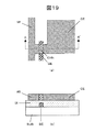
本実施の形態5における半導体装置の製造方法は以下の通りである(各工程の詳細は実施の形態1に準ずる)。まず、透明基板SUB上に図18(a)に示すように、金属によりゲート電極GEが形成される。そして、ゲート電極GEを覆うようにして、ゲート絶縁膜GIが形成される。その後、ゲート絶縁膜GI上に透明導電膜TCLが形成され、さらにその上にネガレジストNRESが塗布され、透明基板SUBの裏面側よりネガレジストNRESが露光される(裏面露光)。この露光工程においては、金属よりなるゲート電極GEがマスクとして働き、それ以外の部材は露光光を透過するため、ゲート電極GEに対して自己整合的にネガレジストNRESを露光することができる。続いて、ネガレジストNRESが図18(b)に示すようにパターニングされる。その後、酸素系プラズマ照射、酸素雰囲気アニールなどを行ない、ネガレジストNRES開口部より透明導電膜TCLの一部を改質(酸素導入によるキャリア濃度低減)し、チャネル層CHNが形成される。この際、チャネル層CHNにより分断された透明導電膜TCLの残りの部分はソース電極SEおよびドレイン電極DEとなる。最後にネガレジストNRESを除去し、図18(d)に示すようなTFTを得る。 The manufacturing method of the semiconductor device in the fifth embodiment is as follows (the details of each step are the same as those in the first embodiment). First, as shown in FIG. 18A, the gate electrode GE is formed of metal on the transparent substrate SUB. Then, the gate insulating film GI is formed so as to cover the gate electrode GE. Thereafter, a transparent conductive film TCL is formed on the gate insulating film GI, a negative resist NRES is further applied thereon, and the negative resist NRES is exposed from the back side of the transparent substrate SUB (backside exposure). In this exposure process, the gate electrode GE made of metal serves as a mask and the other members transmit the exposure light, so that the negative resist NRES can be exposed in a self-aligned manner with respect to the gate electrode GE. Subsequently, the negative resist NRES is patterned as shown in FIG. Thereafter, oxygen-based plasma irradiation, oxygen atmosphere annealing, and the like are performed, and a part of the transparent conductive film TCL is modified from the negative resist NRES opening (reducing carrier concentration by introducing oxygen) to form a channel layer CHN. At this time, the remaining portion of the transparent conductive film TCL divided by the channel layer CHN becomes the source electrode SE and the drain electrode DE. Finally, the negative resist NRES is removed to obtain a TFT as shown in FIG.
図19は本実施の形態5においてTFTと同時に配線WIや容量電極CEを形成した場合の半導体装置の構成を示す図である。図19(a)が上面図、図19(b)がA−A’間の断面図である。 FIG. 19 is a diagram showing a configuration of a semiconductor device when the wiring WI and the capacitance electrode CE are formed simultaneously with the TFT in the fifth embodiment. FIG. 19A is a top view, and FIG. 19B is a cross-sectional view taken along A-A ′.
なお、本実施の形態5における各部材は実施の形態1に示したのと同様の材料によって形成されている。 Each member in the fifth embodiment is formed of the same material as that shown in the first embodiment.
以上、本実施の形態5における自己整合型酸化物TFTによれば、図1に示すような、表面露光のみを用いて形成した際に生じていたソース電極SEおよびドレイン電極DEとゲート電極GEとの間のオーバラップOL、ならびにこのオーバラップOLに起因して生じていた寄生容量CPの発生を抑制することができる。また、チャネル層CHN、ソース電極SE、ドレイン電極DE、さらには必要に応じて配線WIや容量電極CEを同一の膜より一体に形成することができるため、チャネル層とソース・ドレイン電極との間のヘテロ接合による接触抵抗を排除した半導体装置を提供するこができる。また、製造工程が簡易になるため、製造コストが低い半導体装置を提供することができる。 As described above, according to the self-aligned oxide TFT according to the fifth embodiment, the source electrode SE, the drain electrode DE, and the gate electrode GE that are generated when only surface exposure is performed as shown in FIG. And the generation of the parasitic capacitance CP caused by the overlap OL can be suppressed. In addition, since the channel layer CHN, the source electrode SE, the drain electrode DE, and also the wiring WI and the capacitor electrode CE can be integrally formed from the same film as necessary, the channel layer and the source / drain electrodes are not formed. It is possible to provide a semiconductor device that eliminates contact resistance due to the heterojunction. Further, since the manufacturing process is simplified, a semiconductor device with low manufacturing cost can be provided.
(実施の形態6)
図20は、本実施の形態6における半導体装置の構成および製造方法を示す図である。半導体装置としていわゆるボトムゲート型酸化物TFTを挙げている。ここでいうボトムゲートとは、チャネル層CHNよりも下層にゲート電極GEが形成されている構造のことを示している。
(Embodiment 6)
FIG. 20 is a diagram showing the configuration of the semiconductor device and the manufacturing method thereof in the sixth embodiment. A so-called bottom gate type oxide TFT is cited as a semiconductor device. The bottom gate here indicates a structure in which the gate electrode GE is formed below the channel layer CHN.
本実施の形態6における半導体装置の製造方法は以下の通りである(各工程の詳細は実施の形態1に準ずる)。まず、透明基板SUB上に図20(a)に示すように、金属によりゲート電極GEが形成される。そして、ゲート電極GEを覆うようにして、ゲート絶縁膜GIが形成される。その後、ゲート絶縁膜GI上に透明半導体膜TSが形成され、さらにその上にポジレジストPRESが塗布され、透明基板SUBの裏面側よりポジレジストPRESが露光される(裏面露光)。この露光工程においては、金属よりなるゲート電極GEがマスクとして働き、それ以外の部材は露光光を透過するため、ゲート電極GEに対して自己整合的にポジレジストPRESを露光することができる。続いて、ポジレジストPRESが図20(b)に示すようにパターニングされる。その後、プラズマ照射、レーザ照射、還元雰囲気アニールなどを行ない、ポジレジストPRES開口部より透明半導体膜TSの一部を改質(酸素引き抜き、あるいは水素導入によるキャリア濃度増大)し、ソース電極SE、ドレイン電極DEが形成される。この際、透明半導体膜TSの残りの部分はチャネル層CHNとなる。最後にポジレジストPRESを除去し、図20(d)に示すようなTFTを得る。本実施の形態6においてもTFTと同時に配線WIや容量電極CEを形成し、図19のような構成をとることもできる。 The manufacturing method of the semiconductor device in the sixth embodiment is as follows (the details of each process are the same as those in the first embodiment). First, as shown in FIG. 20A, the gate electrode GE is formed of metal on the transparent substrate SUB. Then, the gate insulating film GI is formed so as to cover the gate electrode GE. Thereafter, a transparent semiconductor film TS is formed on the gate insulating film GI, and further, a positive resist PRES is applied thereon, and the positive resist PRES is exposed from the back side of the transparent substrate SUB (backside exposure). In this exposure step, the gate electrode GE made of metal serves as a mask and the other members transmit the exposure light. Therefore, the positive resist PRES can be exposed in a self-aligned manner with respect to the gate electrode GE. Subsequently, the positive resist PRES is patterned as shown in FIG. Thereafter, plasma irradiation, laser irradiation, reducing atmosphere annealing, etc. are performed to modify a part of the transparent semiconductor film TS from the positive resist PRES opening (extraction of oxygen or increase of carrier concentration by introduction of hydrogen), and the source electrode SE, drain An electrode DE is formed. At this time, the remaining portion of the transparent semiconductor film TS becomes the channel layer CHN. Finally, the positive resist PRES is removed to obtain a TFT as shown in FIG. Also in the sixth embodiment, the wiring WI and the capacitor electrode CE can be formed simultaneously with the TFT, and the configuration as shown in FIG. 19 can be taken.
なお、本実施の形態6における各部材は実施の形態1に示したのと同様の材料によって形成されている。 Each member in the sixth embodiment is formed of the same material as that shown in the first embodiment.
以上、本実施の形態6における自己整合型酸化物TFTによれば、図1に示すような、表面露光のみを用いて形成した際に生じていたソース電極SEおよびドレイン電極DEとゲート電極GEとの間のオーバラップOL、ならびにこのオーバラップOLに起因して生じていた寄生容量CPの発生を抑制することができる。また、チャネル層CHN、ソース電極SE、ドレイン電極DE、さらには必要に応じて配線WIや容量電極CEを同一の膜より一体に形成することができるため、チャネル層とソース・ドレイン電極との間のヘテロ接合による接触抵抗を排除した半導体装置を提供するこができる。また、製造工程が簡易になるため、製造コストが低い半導体装置を提供することができる。 As described above, according to the self-aligned oxide TFT according to the sixth embodiment, the source electrode SE, the drain electrode DE, and the gate electrode GE that are generated when only surface exposure is performed as shown in FIG. And the generation of the parasitic capacitance CP caused by the overlap OL can be suppressed. In addition, since the channel layer CHN, the source electrode SE, the drain electrode DE, and also the wiring WI and the capacitor electrode CE can be integrally formed from the same film as necessary, the channel layer and the source / drain electrodes are not formed. It is possible to provide a semiconductor device that eliminates contact resistance due to the heterojunction. Further, since the manufacturing process is simplified, a semiconductor device with low manufacturing cost can be provided.
(実施の形態7)
図21は本実施の形態5における半導体装置の構成を示す図である。実施の形態1〜6に示す構造の酸化物TFTを用いてアンテナ共振回路AR、整流器RCT、変調器MOD、デジタル回路DGCなどを構成し、無線タグを形成している。無線タグはリーダRDまたはライタWRと無線で通信を行うことができるようになっている。無線タグでは、リーダRDやライタWRとの無線通信を行なうが、高周波での動作が要求される。このとき、前記実施の形態1〜6に示す自己整合型酸化物TFTでは、寄生容量が小さいため高周波での動作が可能になる。これにより、前記実施の形態1〜6における自己整合型酸化物TFTを使用した回路の高速化を図ることができる。このことから、前記実施の形態1〜6に示す自己整合型酸化物TFTは、高周波動作が必要とされる無線タグの使用に適しているといえる。
(Embodiment 7)
FIG. 21 is a diagram showing a configuration of the semiconductor device according to the fifth embodiment. An antenna resonant circuit AR, a rectifier RCT, a modulator MOD, a digital circuit DGC, and the like are formed using the oxide TFTs having the structures described in
(実施の形態8)
図22は本実施の形態8における半導体装置の構成を示す図である。本実施の形態8では、前記実施の形態1〜6の構造を有する酸化物TFTを構成要素とする素子が基板SUB上にアレイ状に配置されている。前記実施の形態1〜6に示す酸化物TFTを、アレイ内の各素子のスイッチングや駆動用のトランジスタに用いることはもちろん、この酸化物TFTのゲート電極GEと接続されるゲート線GLに信号を送るゲート線駆動回路GDCや、この酸化物TFTのソース電極SEあるいはドレイン電極DEと接続されるデータ線DLに信号を送るデータ線駆動回路DDCを構成するトランジスタに用いてもよい。この場合、各素子の酸化物TFTとゲート線駆動回路GDCあるいはデータ線駆動回路DDC内の酸化物TFTを並行して形成することができる。
(Embodiment 8)
FIG. 22 shows a configuration of the semiconductor device according to the eighth embodiment. In the eighth embodiment, elements having the oxide TFTs having the structures of the first to sixth embodiments as constituent elements are arranged in an array on the substrate SUB. The oxide TFTs shown in the first to sixth embodiments are used not only for switching and driving transistors of each element in the array, but also for supplying a signal to the gate line GL connected to the gate electrode GE of the oxide TFT. You may use for the gate line drive circuit GDC to send, and the transistor which comprises the data line drive circuit DDC which sends a signal to the data line DL connected with the source electrode SE or drain electrode DE of this oxide TFT. In this case, the oxide TFT of each element and the oxide TFT in the gate line driving circuit GDC or the data line driving circuit DDC can be formed in parallel.
アクティブマトリクス型液晶表示装置に上述したアレイを適用する場合、各素子は、例えば、図23に示すような構成になる。図中x方向に延在するゲート線GLに走査信号が供給されると、酸化物TFTがオンし、このオンされた酸化物TFTを通して、図中y方向に延在するデータ線DLからの映像信号が画素電極PEに供給される。なお、ゲート線GLは図中y方向に並設され、データ線DLは図中x方向に並設され、隣接する一対のゲート線GLと隣接する一対のドレイン線DLで囲まれる領域(画素領域)に画素電極PEが配置されている。この場合、例えば、データ線DLがソース電極SEと電気的に接続され、画素電極PEがドレイン電極DEと電気的に接続される。あるいは、データ線DLがソース電極SEを兼ねてもよい。また、液晶表示装置に限らず有機EL表示装置などに上述したアレイを適用してもよい。この場合、画素回路を構成するトランジスタに酸化物TFTを適用する。さらには、上述したアレイを記憶素子に適用し、選択トランジスタに酸化物TFTを適用してもよい。 When the above-described array is applied to an active matrix liquid crystal display device, each element has a configuration as shown in FIG. 23, for example. When a scanning signal is supplied to the gate line GL extending in the x direction in the figure, the oxide TFT is turned on, and the image from the data line DL extending in the y direction in the figure through the turned on oxide TFT. A signal is supplied to the pixel electrode PE. Note that the gate lines GL are juxtaposed in the y direction in the drawing, the data lines DL are juxtaposed in the x direction in the drawing, and a region (pixel region) surrounded by a pair of adjacent drain lines DL and a pair of adjacent gate lines GL. ) Is provided with a pixel electrode PE. In this case, for example, the data line DL is electrically connected to the source electrode SE, and the pixel electrode PE is electrically connected to the drain electrode DE. Alternatively, the data line DL may also serve as the source electrode SE. Further, the above-described array may be applied not only to the liquid crystal display device but also to an organic EL display device. In this case, an oxide TFT is applied to a transistor constituting the pixel circuit. Further, the above-described array may be applied to a memory element, and an oxide TFT may be applied to a selection transistor.
以上、本発明者によってなされた発明を実施の形態に基づき具体的に説明したが、本発明は前記実施の形態に限定されるものではなく、その要旨を逸脱しない範囲で種々変更可能である。 As mentioned above, the invention made by the present inventor has been specifically described based on the embodiments. However, the present invention is not limited to the above-described embodiments, and various modifications can be made without departing from the scope of the invention.
本発明における半導体装置は、無線タグ、記憶素子アレイなどを構成するトランジスタや周辺回路などに適用できる。また、透過型、反射型、半透過型の各液晶表示装置、並びに有機EL表示装置などの各画素を駆動するトランジスタや周辺回路などにも適用できる。 The semiconductor device of the present invention can be applied to a transistor, a peripheral circuit, or the like included in a wireless tag, a memory element array, or the like. Further, the present invention can also be applied to transistors, peripheral circuits, and the like that drive pixels such as transmissive, reflective, and transflective liquid crystal display devices, and organic EL display devices.
AR アンテナ共振回路
CE 容量電極
CHN チャネル層
CHN2 チャネル層
CP 寄生容量
DDC データ線駆動回路
DE ドレイン電極
DE2 ドレイン電極
DGC デジタル回路
DL データ線
GDC ゲート線駆動回路
GE ゲート電極
GE2 ゲート電極
GI ゲート絶縁膜
GL ゲート線
IF 絶縁膜
LWI 下層配線
MOD 変調器
NRES ネガレジスト
OL オーバラップ
PE 画素電極
PM フォトマスク
PRES ポジレジスト
RCT 整流器
RD リーダ
SE ソース電極
SE2 ソース電極
SUB 基板
TCL 透明導電膜
TFT 酸化物TFT
UWI 上層配線
WI 配線
WR ライタ
AR antenna resonance circuit CE capacitive electrode CHN channel layer CHN2 channel layer CP parasitic capacitance DDC data line drive circuit DE drain electrode DE2 drain electrode DGC digital circuit DL data line GDC gate line drive circuit GE gate electrode GE2 gate electrode GI gate insulating film GL gate Line IF Insulating film LWI Lower layer wiring MOD Modulator NRES Negative resist OL Overlap PE Pixel electrode PM Photomask PRES Positive resist RCT Rectifier RD Reader SE Source electrode SE2 Source electrode SUB Substrate TCL Transparent conductive film TFT Oxide TFT
UWI Upper layer wiring WI wiring WR Writer
Claims (16)
前記ソース電極と前記ドレイン電極と前記チャネル膜の上にゲート絶縁膜を形成し、
前記ゲート絶縁膜上に、導電膜を形成し、
前記導電膜上にネガレジストを塗布し、
前記ソース電極と前記ドレイン電極と共に前記第1配線をマスクとして、前記基板の裏面側から前記ネガレジストを露光し、
前記ネガレジストの露光部分を残し前記ネガレジストを除去し、
前記露光部分をエッチングマスクとして前記導電膜をエッチングし、
前記導電膜上にレジストを塗布し、
前記基板の表面側から前記レジストを露光し、
露光後の前記レジストをエッチングマスクとして前記導電膜を再度エッチングすることで、ゲート電極と共に第2配線を形成し、
前記第1配線直上の前記第2配線の分断部分に第3配線を形成し接続することを特徴とする半導体装置の製造方法。 Forming a first wiring along with the source electrode and the drain electrode of a metal film on a substrate, a channel layer is formed of an oxide semiconductor,
Forming a gate insulating film on the source electrode, the drain electrode and the channel film;
Forming a conductive film on the gate insulating film;
Apply a negative resist on the conductive film,
Using the first wiring as a mask together with the source electrode and the drain electrode, exposing the negative resist from the back side of the substrate,
Removing the negative resist leaving an exposed portion of the negative resist;
Etching the conductive film using the exposed portion as an etching mask,
A resist is applied on the conductive film,
Exposing the resist from the surface side of the substrate;
Etching the conductive film again using the resist after exposure as an etching mask to form a second wiring together with the gate electrode ,
3. A method of manufacturing a semiconductor device, comprising: forming and connecting a third wiring to a part of the second wiring immediately above the first wiring .
前記裏面露光の光源として、水銀ランプのi線を用いることを特徴とする半導体装置の製造方法。 In the manufacturing method of Claim 1,
A method of manufacturing a semiconductor device, wherein an i-line of a mercury lamp is used as a light source for the back exposure.
前記基板は、プラスチックフィルムからなることを特徴とする半導体装置の製造方法。 In the manufacturing method of Claim 1,
The method of manufacturing a semiconductor device, wherein the substrate is made of a plastic film.
前記チャネル膜は、Zn−O、In-O、Ga-O、Sn-O、In−Ga−Zn−O、Zn−Sn−O、In−Sn−O、In−Zn−O、Ga−Zn−O、In−Ga−Oの何れか一つから成ることを特徴とする半導体装置の製造方法。 In the manufacturing method of Claim 1,
The channel film includes Zn—O, In—O, Ga—O, Sn—O, In—Ga—Zn—O, Zn—Sn—O, In—Sn—O, In—Zn—O, and Ga—Zn. A method for manufacturing a semiconductor device, comprising any one of -O and In-Ga-O.
前記ゲート絶縁膜は、Si−O、Al−O、Si−Nの何れか一つから成ることを特徴とする半導体装置の製造方法。 In the manufacturing method of Claim 1,
The method of manufacturing a semiconductor device, wherein the gate insulating film is made of any one of Si-O, Al-O, and Si-N.
前記導電膜は、In-Sn-O、Al−Zn-O、Sn−Oの何れか一つから成ることを特徴とする半導体装置の製造方法。 In the manufacturing method of Claim 1,
The method of manufacturing a semiconductor device, wherein the conductive film is made of any one of In-Sn-O, Al-Zn-O, and Sn-O.
前記基板と、チャネル膜と、ゲート絶縁膜と、導電膜は透明であり、
前記金属膜は不透明であることを特徴とする半導体装置の製造方法。 In the manufacturing method of Claim 1,
The substrate, the channel film, the gate insulating film, and the conductive film are transparent,
A method of manufacturing a semiconductor device, wherein the metal film is opaque.
前記ゲート電極と前記基板の上にゲート絶縁膜を形成し、
前記ゲート絶縁膜上に酸化物半導体によりチャネル膜を形成し、
前記チャネル膜上に導電膜を形成し、
前記導電膜上にネガレジストを塗布し、
前記ゲート電極と共に前記第1配線をマスクとして、前記基板の裏面側から前記ネガレジストを露光し、
前記ネガレジストの露光部分を残し前記ネガレジストを除去し、
前記露光部分をエッチングマスクとして前記導電膜をエッチングし、
前記導電膜上にレジストを塗布し、
前記基板の表面側から前記レジストを露光し、
露光後の前記レジストをエッチングマスクとして前記導電膜を再度エッチングすることで、ソース電極とドレイン電極と共に第2配線を形成し、
前記第1配線直上の前記第2配線の分断部分に第3配線を形成し接続することを特徴とする半導体装置の製造方法。 Forming a first wiring with a gate electrode by a metal film on the substrate;
Forming a gate insulating film on the gate electrode and the substrate;
Forming a channel film from an oxide semiconductor on the gate insulating film;
Forming a conductive film on the channel film;
Apply a negative resist on the conductive film,
Using the first wiring as a mask together with the gate electrode, exposing the negative resist from the back side of the substrate,
Removing the negative resist leaving an exposed portion of the negative resist;
Etching the conductive film using the exposed portion as an etching mask,
A resist is applied on the conductive film,
Exposing the resist from the surface side of the substrate;
Etching the conductive film again using the exposed resist as an etching mask to form the second wiring together with the source electrode and the drain electrode ,
3. A method of manufacturing a semiconductor device, comprising: forming and connecting a third wiring to a part of the second wiring immediately above the first wiring .
前記裏面露光の光源として、水銀ランプのi線を用いることを特徴とする半導体装置の製造方法。 The manufacturing method according to claim 8, wherein
A method of manufacturing a semiconductor device, wherein an i-line of a mercury lamp is used as a light source for the back exposure.
前記基板は、プラスチックフィルムからなることを特徴とする半導体装置の製造方法。 The manufacturing method according to claim 8, wherein
The method of manufacturing a semiconductor device, wherein the substrate is made of a plastic film.
前記チャネル膜は、Zn−O、In-O、Ga-O、Sn-O、In−Ga−Zn−O、Zn−Sn−O、In−Sn−O、In−Zn−O、Ga−Zn−O、In−Ga−Oの何れか一つから成ることを特徴とする半導体装置の製造方法。 The manufacturing method according to claim 8, wherein
The channel film includes Zn—O, In—O, Ga—O, Sn—O, In—Ga—Zn—O, Zn—Sn—O, In—Sn—O, In—Zn—O, and Ga—Zn. A method for manufacturing a semiconductor device, comprising any one of -O and In-Ga-O.
前記ゲート絶縁膜は、Si−O、Al−O、Si−Nの何れか一つから成ることを特徴とする半導体装置の製造方法。 The manufacturing method according to claim 8, wherein
The method of manufacturing a semiconductor device, wherein the gate insulating film is made of any one of Si-O, Al-O, and Si-N.
前記導電膜は、In-Sn-O、Al−Zn-O、Sn−Oの何れか一つから成ることを特徴とする半導体装置の製造方法。 The manufacturing method according to claim 8, wherein
The method of manufacturing a semiconductor device, wherein the conductive film is made of any one of In-Sn-O, Al-Zn-O, and Sn-O.
前記基板と、チャネル膜と、ゲート絶縁膜と、導電膜は透明であり、
前記金属膜は不透明であることを特徴とする半導体装置の製造方法。 The manufacturing method according to claim 8, wherein
The substrate, the channel film, the gate insulating film, and the conductive film are transparent,
A method of manufacturing a semiconductor device, wherein the metal film is opaque.
前記ソース電極と前記ドレイン電極と前記チャネル膜の上にゲート絶縁膜を形成し、
前記ゲート絶縁膜上に、導電膜を形成し、
前記導電膜上にネガレジストを塗布し、
前記ソース電極と前記ドレイン電極と共に前記第1配線をマスクとして、前記基板の裏面側から前記ネガレジストを露光し、
前記ネガレジストの露光部分を残し前記ネガレジストを除去し、
前記露光部分をエッチングマスクとして前記導電膜をエッチングし、
前記導電膜上にレジストを塗布し、
前記基板の表面側から前記レジストを露光し、
露光後の前記レジストをエッチングマスクとする前記導電膜のエッチングにより、ゲート電極と共に第2配線を形成し、
前記第1配線直上の前記第2配線の分断部分に第3配線を形成し接続することにより製造された半導体装置。 Forming a first wiring along with the source electrode and the drain electrode of a metal film on a substrate, a channel layer is formed of an oxide semiconductor,
Forming a gate insulating film on the source electrode, the drain electrode and the channel film;
Forming a conductive film on the gate insulating film;
Apply a negative resist on the conductive film,
Using the first wiring as a mask together with the source electrode and the drain electrode, exposing the negative resist from the back side of the substrate,
Removing the negative resist leaving an exposed portion of the negative resist;
Etching the conductive film using the exposed portion as an etching mask,
A resist is applied on the conductive film,
Exposing the resist from the surface side of the substrate;
A second wiring is formed together with the gate electrode by etching the conductive film using the resist after exposure as an etching mask .
A semiconductor device manufactured by forming and connecting a third wiring to a portion of the second wiring directly above the first wiring .
前記ゲート電極と前記基板の上にゲート絶縁膜を形成し、
前記ゲート絶縁膜上に酸化物半導体によりチャネル膜を形成し、
前記チャネル膜上に導電膜を形成し、
前記導電膜上にネガレジストを塗布し、
前記ゲート電極と共に前記第1配線をマスクとして、前記基板の裏面側から前記ネガレジストを露光し、
前記ネガレジストの露光部分を残し前記ネガレジストを除去し、
前記露光部分をエッチングマスクとして前記導電膜をエッチングし、
前記導電膜上にレジストを塗布し、
前記基板の表面側から前記レジストを露光し、
露光後の前記レジストをエッチングマスクとして前記導電膜を再度エッチングすることで、ソース電極とドレイン電極と共に第2配線を形成し、
前記第1配線直上の前記第2配線の分断部分に第3配線を形成し接続することにより製造された半導体装置。 Forming a first wiring with a gate electrode by a metal film on the substrate;
Forming a gate insulating film on the gate electrode and the substrate;
Forming a channel film from an oxide semiconductor on the gate insulating film;
Forming a conductive film on the channel film;
Apply a negative resist on the conductive film,
Using the first wiring as a mask together with the gate electrode, exposing the negative resist from the back side of the substrate,
Removing the negative resist leaving an exposed portion of the negative resist;
Etching the conductive layer using the exposed portion as an etching mask,
A resist is applied on the conductive film,
Exposing the resist from the surface side of the substrate;
Etching the conductive film again using the exposed resist as an etching mask to form the second wiring together with the source electrode and the drain electrode ,
A semiconductor device manufactured by forming and connecting a third wiring to a portion of the second wiring directly above the first wiring .
Priority Applications (3)
| Application Number | Priority Date | Filing Date | Title |
|---|---|---|---|
| JP2009191589A JP5500907B2 (en) | 2009-08-21 | 2009-08-21 | Semiconductor device and manufacturing method thereof |
| US12/838,451 US8314032B2 (en) | 2009-08-21 | 2010-07-17 | Semiconductor device and method for manufacturing the same |
| KR1020100073549A KR101126798B1 (en) | 2009-08-21 | 2010-07-29 | Semiconductor device and method for manufacturing the same |
Applications Claiming Priority (1)
| Application Number | Priority Date | Filing Date | Title |
|---|---|---|---|
| JP2009191589A JP5500907B2 (en) | 2009-08-21 | 2009-08-21 | Semiconductor device and manufacturing method thereof |
Publications (3)
| Publication Number | Publication Date |
|---|---|
| JP2011044575A JP2011044575A (en) | 2011-03-03 |
| JP2011044575A5 JP2011044575A5 (en) | 2012-04-26 |
| JP5500907B2 true JP5500907B2 (en) | 2014-05-21 |
Family
ID=43604593
Family Applications (1)
| Application Number | Title | Priority Date | Filing Date |
|---|---|---|---|
| JP2009191589A Expired - Fee Related JP5500907B2 (en) | 2009-08-21 | 2009-08-21 | Semiconductor device and manufacturing method thereof |
Country Status (3)
| Country | Link |
|---|---|
| US (1) | US8314032B2 (en) |
| JP (1) | JP5500907B2 (en) |
| KR (1) | KR101126798B1 (en) |
Families Citing this family (28)
| Publication number | Priority date | Publication date | Assignee | Title |
|---|---|---|---|---|
| WO2011074407A1 (en) | 2009-12-18 | 2011-06-23 | Semiconductor Energy Laboratory Co., Ltd. | Semiconductor device and method for manufacturing the same |
| US9209314B2 (en) | 2010-06-16 | 2015-12-08 | Semiconductor Energy Laboratory Co., Ltd. | Field effect transistor |
| WO2012002186A1 (en) | 2010-07-02 | 2012-01-05 | Semiconductor Energy Laboratory Co., Ltd. | Semiconductor device |
| WO2012014786A1 (en) * | 2010-07-30 | 2012-02-02 | Semiconductor Energy Laboratory Co., Ltd. | Semicondcutor device and manufacturing method thereof |
| US8704230B2 (en) | 2010-08-26 | 2014-04-22 | Semiconductor Energy Laboratory Co., Ltd. | Semiconductor device and manufacturing method thereof |
| JP2012256821A (en) | 2010-09-13 | 2012-12-27 | Semiconductor Energy Lab Co Ltd | Memory device |
| US9443984B2 (en) | 2010-12-28 | 2016-09-13 | Semiconductor Energy Laboratory Co., Ltd. | Semiconductor device and manufacturing method thereof |
| US8829512B2 (en) | 2010-12-28 | 2014-09-09 | Semiconductor Energy Laboratory Co., Ltd. | Semiconductor device and method for manufacturing the same |
| GB2489682B (en) | 2011-03-30 | 2015-11-04 | Pragmatic Printing Ltd | Electronic device and its method of manufacture |
| GB2522565B (en) | 2011-06-27 | 2016-02-03 | Pragmatic Printing Ltd | Transistor and its method of manufacture |
| GB201202544D0 (en) * | 2012-02-14 | 2012-03-28 | Pragmatic Printing Ltd | Electronic devices |
| JP2013012610A (en) * | 2011-06-29 | 2013-01-17 | Dainippon Printing Co Ltd | Thin film transistor and manufacturing method of the same |
| US9082663B2 (en) | 2011-09-16 | 2015-07-14 | Semiconductor Energy Laboratory Co., Ltd. | Semiconductor device and manufacturing method thereof |
| WO2013047629A1 (en) | 2011-09-29 | 2013-04-04 | Semiconductor Energy Laboratory Co., Ltd. | Semiconductor device |
| JP6026839B2 (en) * | 2011-10-13 | 2016-11-16 | 株式会社半導体エネルギー研究所 | Semiconductor device |
| CN104025301B (en) | 2011-10-14 | 2017-01-18 | 株式会社半导体能源研究所 | Semiconductor device |
| US8796682B2 (en) * | 2011-11-11 | 2014-08-05 | Semiconductor Energy Laboratory Co., Ltd. | Method for manufacturing a semiconductor device |
| US8981367B2 (en) | 2011-12-01 | 2015-03-17 | Semiconductor Energy Laboratory Co., Ltd. | Semiconductor device |
| US9076505B2 (en) | 2011-12-09 | 2015-07-07 | Semiconductor Energy Laboratory Co., Ltd. | Memory device |
| US10002968B2 (en) | 2011-12-14 | 2018-06-19 | Semiconductor Energy Laboratory Co., Ltd. | Semiconductor device and display device including the same |
| US8796683B2 (en) | 2011-12-23 | 2014-08-05 | Semiconductor Energy Laboratory Co., Ltd. | Semiconductor device |
| US9006024B2 (en) * | 2012-04-25 | 2015-04-14 | Semiconductor Energy Laboratory Co., Ltd. | Method for manufacturing semiconductor device |
| TWI511200B (en) * | 2013-07-25 | 2015-12-01 | Ye Xin Technology Consulting Co Ltd | Manufacturing method of display panel |
| US9397153B2 (en) * | 2013-09-23 | 2016-07-19 | Semiconductor Energy Laboratory Co., Ltd. | Semiconductor device |
| JP2016076541A (en) | 2014-10-03 | 2016-05-12 | ソニー株式会社 | Thin film transistor, thin film transistor manufacturing method and display device |
| US9991394B2 (en) * | 2015-02-20 | 2018-06-05 | Semiconductor Energy Laboratory Co., Ltd. | Semiconductor device and fabrication method thereof |
| JP6583812B2 (en) * | 2015-06-24 | 2019-10-02 | 国立研究開発法人物質・材料研究機構 | Manufacturing method of multi-layered thin film transistor |
| JP6965894B2 (en) * | 2016-12-12 | 2021-11-10 | 住友電気工業株式会社 | Semiconductor device manufacturing method |
Family Cites Families (23)
| Publication number | Priority date | Publication date | Assignee | Title |
|---|---|---|---|---|
| JP2913300B2 (en) * | 1985-09-26 | 1999-06-28 | セイコーインスツルメンツ株式会社 | Method for manufacturing thin film transistor device |
| JPS62152174A (en) | 1985-12-25 | 1987-07-07 | Matsushita Electric Ind Co Ltd | Manufacture of thin-film transistor |
| JPH02128432A (en) * | 1988-11-08 | 1990-05-16 | Fuji Xerox Co Ltd | Manufacture of thin film transistor |
| JPH02211635A (en) * | 1989-02-13 | 1990-08-22 | Seiko Epson Corp | Manufacture of field-effect transistor |
| JPH02273935A (en) * | 1989-04-14 | 1990-11-08 | Sanyo Electric Co Ltd | Manufacture of thin film transistor |
| GB9114018D0 (en) * | 1991-06-28 | 1991-08-14 | Philips Electronic Associated | Thin-film transistor manufacture |
| US5441905A (en) * | 1993-04-29 | 1995-08-15 | Industrial Technology Research Institute | Process of making self-aligned amorphous-silicon thin film transistors |
| JPH06333949A (en) | 1993-05-21 | 1994-12-02 | Kyocera Corp | Manufacture of thin film transistor |
| JPH07211914A (en) * | 1994-01-13 | 1995-08-11 | Dainippon Printing Co Ltd | Thin film transistor and its manufacture |
| JPH08228011A (en) * | 1994-12-14 | 1996-09-03 | Toshiba Corp | Semiconductor device and manufacture thereof |
| GB9907019D0 (en) * | 1999-03-27 | 1999-05-19 | Koninkl Philips Electronics Nv | Thin film transistors and their manufacture |
| JP3447619B2 (en) * | 1999-06-25 | 2003-09-16 | 株式会社東芝 | Active matrix substrate manufacturing method, intermediate transfer substrate |
| GB9919913D0 (en) * | 1999-08-24 | 1999-10-27 | Koninkl Philips Electronics Nv | Thin-film transistors and method for producing the same |
| GB9929615D0 (en) * | 1999-12-15 | 2000-02-09 | Koninkl Philips Electronics Nv | Method of manufacturing an active matrix device |
| JP2003168645A (en) * | 2001-12-03 | 2003-06-13 | Hitachi Ltd | Semiconductor thin film device, its manufacturing method, and image display device |
| US7211825B2 (en) * | 2004-06-14 | 2007-05-01 | Yi-Chi Shih | Indium oxide-based thin film transistors and circuits |
| TWI294689B (en) * | 2005-09-14 | 2008-03-11 | Ind Tech Res Inst | Method of tft manufacturing and a base-board substrate structure |
| JP2008171989A (en) * | 2007-01-11 | 2008-07-24 | Toppan Printing Co Ltd | Field effect transistor and manufacturing method thereof |
| KR100857455B1 (en) * | 2007-04-17 | 2008-09-08 | 한국전자통신연구원 | Method of fabricating thin film transistor including ald deposited protection layer on the oxide semiconductor |
| JP5213421B2 (en) | 2007-12-04 | 2013-06-19 | キヤノン株式会社 | Oxide semiconductor thin film transistor |
| JP5405850B2 (en) * | 2009-02-17 | 2014-02-05 | 株式会社日立製作所 | Method for manufacturing field effect transistor having oxide semiconductor |
| JP2010199457A (en) * | 2009-02-27 | 2010-09-09 | Dainippon Printing Co Ltd | Method of manufacturing transistor element |
| JP2010199458A (en) * | 2009-02-27 | 2010-09-09 | Dainippon Printing Co Ltd | Method of manufacturing transistor element |
-
2009
- 2009-08-21 JP JP2009191589A patent/JP5500907B2/en not_active Expired - Fee Related
-
2010
- 2010-07-17 US US12/838,451 patent/US8314032B2/en not_active Expired - Fee Related
- 2010-07-29 KR KR1020100073549A patent/KR101126798B1/en not_active IP Right Cessation
Also Published As
| Publication number | Publication date |
|---|---|
| JP2011044575A (en) | 2011-03-03 |
| US20110042667A1 (en) | 2011-02-24 |
| KR101126798B1 (en) | 2012-03-23 |
| KR20110020172A (en) | 2011-03-02 |
| US8314032B2 (en) | 2012-11-20 |
Similar Documents
| Publication | Publication Date | Title |
|---|---|---|
| JP5500907B2 (en) | Semiconductor device and manufacturing method thereof | |
| US10403757B2 (en) | Top-gate self-aligned metal oxide semiconductor TFT and method of making the same | |
| US10109647B2 (en) | MOTFT with un-patterned etch-stop | |
| JP5325446B2 (en) | Semiconductor device and manufacturing method thereof | |
| US7550772B2 (en) | Image display device and manufacturing method thereof | |
| US8202770B2 (en) | Semiconductor structure of a display device and method for fabricating the same | |
| JP2010021170A (en) | Semiconductor device, and method of manufacturing the same | |
| US10209558B2 (en) | Array substrate and manufacturing method thereof, display panel and display device | |
| JP2003273361A (en) | Semiconductor device and manufacturing method thereof | |
| WO2016123974A1 (en) | Thin-film transistor, pixel structure, manufacturing methods therefor, array substrate and display device | |
| WO2016115824A1 (en) | Thin film transistor and array substrate, and manufacturing method therefor | |
| US20100117155A1 (en) | Semiconductor device and production method thereof | |
| TWI495110B (en) | Display panel and method of making the same | |
| US8227302B2 (en) | Semiconductor device, electronic device, and manufacturing method thereof | |
| CN111710725A (en) | Double-gate electrode metal oxide thin film transistor and preparation method thereof | |
| KR102586938B1 (en) | Thin film transistor array panel and method for manufacturing the same | |
| US20130146864A1 (en) | Thin film transistor display panel and manufacturing method thereof | |
| TWI528564B (en) | Thin film transistor and fabricating method thereof | |
| JP2009206388A (en) | Thin film transistor, and manufacturing method thereof | |
| US11502115B2 (en) | Active matrix substrate and method for manufacturing same | |
| US20230187555A1 (en) | Semiconductor device and manufacturing method thereof | |
| WO2023097728A1 (en) | Array substrate and display panel | |
| TWI814369B (en) | Photosensitive device substrate and manufacturing method thereof | |
| JP2010114160A (en) | Semiconductor element, method of manufacturing the same, and display device | |
| JP2023033960A (en) | Active matrix substrate and method for manufacturing the same |
Legal Events
| Date | Code | Title | Description |
|---|---|---|---|
| A521 | Request for written amendment filed |
Free format text: JAPANESE INTERMEDIATE CODE: A523 Effective date: 20120308 |
|
| A621 | Written request for application examination |
Free format text: JAPANESE INTERMEDIATE CODE: A621 Effective date: 20120308 |
|
| A131 | Notification of reasons for refusal |
Free format text: JAPANESE INTERMEDIATE CODE: A131 Effective date: 20131126 |
|
| A521 | Request for written amendment filed |
Free format text: JAPANESE INTERMEDIATE CODE: A523 Effective date: 20140124 |
|
| TRDD | Decision of grant or rejection written | ||
| A01 | Written decision to grant a patent or to grant a registration (utility model) |
Free format text: JAPANESE INTERMEDIATE CODE: A01 Effective date: 20140212 |
|
| A61 | First payment of annual fees (during grant procedure) |
Free format text: JAPANESE INTERMEDIATE CODE: A61 Effective date: 20140311 |
|
| LAPS | Cancellation because of no payment of annual fees |