WO2018123799A1 - 半導体装置 - Google Patents
半導体装置 Download PDFInfo
- Publication number
- WO2018123799A1 WO2018123799A1 PCT/JP2017/045908 JP2017045908W WO2018123799A1 WO 2018123799 A1 WO2018123799 A1 WO 2018123799A1 JP 2017045908 W JP2017045908 W JP 2017045908W WO 2018123799 A1 WO2018123799 A1 WO 2018123799A1
- Authority
- WO
- WIPO (PCT)
- Prior art keywords
- semiconductor device
- thickness
- layer
- metal layer
- semiconductor
- Prior art date
Links
- 239000004065 semiconductor Substances 0.000 title claims abstract description 322
- 239000010410 layer Substances 0.000 claims abstract description 268
- 229910052751 metal Inorganic materials 0.000 claims abstract description 144
- 239000002184 metal Substances 0.000 claims abstract description 144
- 239000000758 substrate Substances 0.000 claims abstract description 103
- 239000012790 adhesive layer Substances 0.000 claims abstract description 78
- 239000012535 impurity Substances 0.000 claims abstract description 55
- 229910052710 silicon Inorganic materials 0.000 claims abstract description 12
- 239000010703 silicon Substances 0.000 claims abstract description 12
- 229910010293 ceramic material Inorganic materials 0.000 claims abstract description 11
- 239000000463 material Substances 0.000 claims description 13
- 239000004020 conductor Substances 0.000 claims description 12
- 239000007769 metal material Substances 0.000 claims description 12
- 229910052709 silver Inorganic materials 0.000 claims description 7
- 239000000470 constituent Substances 0.000 claims description 6
- 239000004332 silver Substances 0.000 claims description 6
- 230000002457 bidirectional effect Effects 0.000 claims description 5
- 210000000746 body region Anatomy 0.000 description 22
- 238000004519 manufacturing process Methods 0.000 description 22
- 239000000853 adhesive Substances 0.000 description 19
- 230000001070 adhesive effect Effects 0.000 description 19
- 230000004048 modification Effects 0.000 description 17
- 238000012986 modification Methods 0.000 description 17
- 238000004364 calculation method Methods 0.000 description 16
- 238000000034 method Methods 0.000 description 16
- 230000000052 comparative effect Effects 0.000 description 13
- 239000010408 film Substances 0.000 description 13
- XUIMIQQOPSSXEZ-UHFFFAOYSA-N Silicon Chemical compound [Si] XUIMIQQOPSSXEZ-UHFFFAOYSA-N 0.000 description 9
- 230000009467 reduction Effects 0.000 description 9
- 238000010586 diagram Methods 0.000 description 8
- 230000008569 process Effects 0.000 description 8
- 239000010949 copper Substances 0.000 description 7
- 239000011521 glass Substances 0.000 description 7
- 230000008859 change Effects 0.000 description 6
- 239000011248 coating agent Substances 0.000 description 6
- 238000000576 coating method Methods 0.000 description 6
- 229910052802 copper Inorganic materials 0.000 description 6
- 230000014509 gene expression Effects 0.000 description 6
- 229910052737 gold Inorganic materials 0.000 description 6
- 239000010931 gold Substances 0.000 description 6
- 229910000679 solder Inorganic materials 0.000 description 6
- PXHVJJICTQNCMI-UHFFFAOYSA-N Nickel Chemical compound [Ni] PXHVJJICTQNCMI-UHFFFAOYSA-N 0.000 description 5
- BQCADISMDOOEFD-UHFFFAOYSA-N Silver Chemical compound [Ag] BQCADISMDOOEFD-UHFFFAOYSA-N 0.000 description 5
- PCHJSUWPFVWCPO-UHFFFAOYSA-N gold Chemical compound [Au] PCHJSUWPFVWCPO-UHFFFAOYSA-N 0.000 description 5
- 239000000523 sample Substances 0.000 description 5
- 230000001629 suppression Effects 0.000 description 5
- RYGMFSIKBFXOCR-UHFFFAOYSA-N Copper Chemical compound [Cu] RYGMFSIKBFXOCR-UHFFFAOYSA-N 0.000 description 4
- KDLHZDBZIXYQEI-UHFFFAOYSA-N Palladium Chemical compound [Pd] KDLHZDBZIXYQEI-UHFFFAOYSA-N 0.000 description 4
- 229910052782 aluminium Inorganic materials 0.000 description 4
- 238000005520 cutting process Methods 0.000 description 4
- 239000011229 interlayer Substances 0.000 description 4
- 239000011347 resin Substances 0.000 description 4
- 229920005989 resin Polymers 0.000 description 4
- VYPSYNLAJGMNEJ-UHFFFAOYSA-N silicon dioxide Inorganic materials O=[Si]=O VYPSYNLAJGMNEJ-UHFFFAOYSA-N 0.000 description 4
- XAGFODPZIPBFFR-UHFFFAOYSA-N aluminium Chemical compound [Al] XAGFODPZIPBFFR-UHFFFAOYSA-N 0.000 description 3
- 229910052759 nickel Inorganic materials 0.000 description 3
- 238000002161 passivation Methods 0.000 description 3
- 239000010409 thin film Substances 0.000 description 3
- 239000010936 titanium Substances 0.000 description 3
- 229910052719 titanium Inorganic materials 0.000 description 3
- 235000012431 wafers Nutrition 0.000 description 3
- 229910052581 Si3N4 Inorganic materials 0.000 description 2
- RTAQQCXQSZGOHL-UHFFFAOYSA-N Titanium Chemical compound [Ti] RTAQQCXQSZGOHL-UHFFFAOYSA-N 0.000 description 2
- 238000004458 analytical method Methods 0.000 description 2
- 239000005388 borosilicate glass Substances 0.000 description 2
- 230000007423 decrease Effects 0.000 description 2
- 238000007599 discharging Methods 0.000 description 2
- 230000000694 effects Effects 0.000 description 2
- 239000003822 epoxy resin Substances 0.000 description 2
- 238000000605 extraction Methods 0.000 description 2
- 229910052809 inorganic oxide Inorganic materials 0.000 description 2
- 229910044991 metal oxide Inorganic materials 0.000 description 2
- 150000004706 metal oxides Chemical class 0.000 description 2
- 239000011368 organic material Substances 0.000 description 2
- 229910052763 palladium Inorganic materials 0.000 description 2
- 229920000647 polyepoxide Polymers 0.000 description 2
- 239000010453 quartz Substances 0.000 description 2
- 229910052594 sapphire Inorganic materials 0.000 description 2
- 239000010980 sapphire Substances 0.000 description 2
- 238000000926 separation method Methods 0.000 description 2
- HQVNEWCFYHHQES-UHFFFAOYSA-N silicon nitride Chemical compound N12[Si]34N5[Si]62N3[Si]51N64 HQVNEWCFYHHQES-UHFFFAOYSA-N 0.000 description 2
- 229910052814 silicon oxide Inorganic materials 0.000 description 2
- 239000005361 soda-lime glass Substances 0.000 description 2
- 229920001187 thermosetting polymer Polymers 0.000 description 2
- WFKWXMTUELFFGS-UHFFFAOYSA-N tungsten Chemical compound [W] WFKWXMTUELFFGS-UHFFFAOYSA-N 0.000 description 2
- 229910052721 tungsten Inorganic materials 0.000 description 2
- 239000010937 tungsten Substances 0.000 description 2
- SMZOUWXMTYCWNB-UHFFFAOYSA-N 2-(2-methoxy-5-methylphenyl)ethanamine Chemical compound COC1=CC=C(C)C=C1CCN SMZOUWXMTYCWNB-UHFFFAOYSA-N 0.000 description 1
- NIXOWILDQLNWCW-UHFFFAOYSA-N 2-Propenoic acid Natural products OC(=O)C=C NIXOWILDQLNWCW-UHFFFAOYSA-N 0.000 description 1
- NIXOWILDQLNWCW-UHFFFAOYSA-M Acrylate Chemical compound [O-]C(=O)C=C NIXOWILDQLNWCW-UHFFFAOYSA-M 0.000 description 1
- 239000004925 Acrylic resin Substances 0.000 description 1
- 229920000178 Acrylic resin Polymers 0.000 description 1
- 238000013459 approach Methods 0.000 description 1
- 230000003111 delayed effect Effects 0.000 description 1
- 238000009713 electroplating Methods 0.000 description 1
- UHESRSKEBRADOO-UHFFFAOYSA-N ethyl carbamate;prop-2-enoic acid Chemical compound OC(=O)C=C.CCOC(N)=O UHESRSKEBRADOO-UHFFFAOYSA-N 0.000 description 1
- 238000011156 evaluation Methods 0.000 description 1
- 230000005669 field effect Effects 0.000 description 1
- 238000000227 grinding Methods 0.000 description 1
- 238000010438 heat treatment Methods 0.000 description 1
- 238000003384 imaging method Methods 0.000 description 1
- 230000001678 irradiating effect Effects 0.000 description 1
- 238000005259 measurement Methods 0.000 description 1
- 238000000691 measurement method Methods 0.000 description 1
- 230000007246 mechanism Effects 0.000 description 1
- QSHDDOUJBYECFT-UHFFFAOYSA-N mercury Chemical compound [Hg] QSHDDOUJBYECFT-UHFFFAOYSA-N 0.000 description 1
- 229910052753 mercury Inorganic materials 0.000 description 1
- 238000005457 optimization Methods 0.000 description 1
- 230000005693 optoelectronics Effects 0.000 description 1
- 239000005011 phenolic resin Substances 0.000 description 1
- 238000003825 pressing Methods 0.000 description 1
- KCTAWXVAICEBSD-UHFFFAOYSA-N prop-2-enoyloxy prop-2-eneperoxoate Chemical compound C=CC(=O)OOOC(=O)C=C KCTAWXVAICEBSD-UHFFFAOYSA-N 0.000 description 1
- 238000004904 shortening Methods 0.000 description 1
- 239000010944 silver (metal) Substances 0.000 description 1
- 238000004381 surface treatment Methods 0.000 description 1
- 238000007740 vapor deposition Methods 0.000 description 1
Images


Classifications
-
- H—ELECTRICITY
- H01—ELECTRIC ELEMENTS
- H01L—SEMICONDUCTOR DEVICES NOT COVERED BY CLASS H10
- H01L29/00—Semiconductor devices adapted for rectifying, amplifying, oscillating or switching, or capacitors or resistors with at least one potential-jump barrier or surface barrier, e.g. PN junction depletion layer or carrier concentration layer; Details of semiconductor bodies or of electrodes thereof ; Multistep manufacturing processes therefor
- H01L29/66—Types of semiconductor device ; Multistep manufacturing processes therefor
- H01L29/68—Types of semiconductor device ; Multistep manufacturing processes therefor controllable by only the electric current supplied, or only the electric potential applied, to an electrode which does not carry the current to be rectified, amplified or switched
- H01L29/76—Unipolar devices, e.g. field effect transistors
- H01L29/772—Field effect transistors
- H01L29/78—Field effect transistors with field effect produced by an insulated gate
- H01L29/7827—Vertical transistors
-
- H—ELECTRICITY
- H01—ELECTRIC ELEMENTS
- H01L—SEMICONDUCTOR DEVICES NOT COVERED BY CLASS H10
- H01L21/00—Processes or apparatus adapted for the manufacture or treatment of semiconductor or solid state devices or of parts thereof
- H01L21/67—Apparatus specially adapted for handling semiconductor or electric solid state devices during manufacture or treatment thereof; Apparatus specially adapted for handling wafers during manufacture or treatment of semiconductor or electric solid state devices or components ; Apparatus not specifically provided for elsewhere
- H01L21/683—Apparatus specially adapted for handling semiconductor or electric solid state devices during manufacture or treatment thereof; Apparatus specially adapted for handling wafers during manufacture or treatment of semiconductor or electric solid state devices or components ; Apparatus not specifically provided for elsewhere for supporting or gripping
- H01L21/6835—Apparatus specially adapted for handling semiconductor or electric solid state devices during manufacture or treatment thereof; Apparatus specially adapted for handling wafers during manufacture or treatment of semiconductor or electric solid state devices or components ; Apparatus not specifically provided for elsewhere for supporting or gripping using temporarily an auxiliary support
-
- H—ELECTRICITY
- H01—ELECTRIC ELEMENTS
- H01L—SEMICONDUCTOR DEVICES NOT COVERED BY CLASS H10
- H01L21/00—Processes or apparatus adapted for the manufacture or treatment of semiconductor or solid state devices or of parts thereof
- H01L21/70—Manufacture or treatment of devices consisting of a plurality of solid state components formed in or on a common substrate or of parts thereof; Manufacture of integrated circuit devices or of parts thereof
- H01L21/71—Manufacture of specific parts of devices defined in group H01L21/70
- H01L21/76—Making of isolation regions between components
-
- H—ELECTRICITY
- H01—ELECTRIC ELEMENTS
- H01L—SEMICONDUCTOR DEVICES NOT COVERED BY CLASS H10
- H01L21/00—Processes or apparatus adapted for the manufacture or treatment of semiconductor or solid state devices or of parts thereof
- H01L21/70—Manufacture or treatment of devices consisting of a plurality of solid state components formed in or on a common substrate or of parts thereof; Manufacture of integrated circuit devices or of parts thereof
- H01L21/77—Manufacture or treatment of devices consisting of a plurality of solid state components or integrated circuits formed in, or on, a common substrate
- H01L21/78—Manufacture or treatment of devices consisting of a plurality of solid state components or integrated circuits formed in, or on, a common substrate with subsequent division of the substrate into plural individual devices
- H01L21/82—Manufacture or treatment of devices consisting of a plurality of solid state components or integrated circuits formed in, or on, a common substrate with subsequent division of the substrate into plural individual devices to produce devices, e.g. integrated circuits, each consisting of a plurality of components
- H01L21/822—Manufacture or treatment of devices consisting of a plurality of solid state components or integrated circuits formed in, or on, a common substrate with subsequent division of the substrate into plural individual devices to produce devices, e.g. integrated circuits, each consisting of a plurality of components the substrate being a semiconductor, using silicon technology
- H01L21/8232—Field-effect technology
- H01L21/8234—MIS technology, i.e. integration processes of field effect transistors of the conductor-insulator-semiconductor type
- H01L21/823475—MIS technology, i.e. integration processes of field effect transistors of the conductor-insulator-semiconductor type interconnection or wiring or contact manufacturing related aspects
-
- H—ELECTRICITY
- H01—ELECTRIC ELEMENTS
- H01L—SEMICONDUCTOR DEVICES NOT COVERED BY CLASS H10
- H01L21/00—Processes or apparatus adapted for the manufacture or treatment of semiconductor or solid state devices or of parts thereof
- H01L21/70—Manufacture or treatment of devices consisting of a plurality of solid state components formed in or on a common substrate or of parts thereof; Manufacture of integrated circuit devices or of parts thereof
- H01L21/77—Manufacture or treatment of devices consisting of a plurality of solid state components or integrated circuits formed in, or on, a common substrate
- H01L21/78—Manufacture or treatment of devices consisting of a plurality of solid state components or integrated circuits formed in, or on, a common substrate with subsequent division of the substrate into plural individual devices
- H01L21/82—Manufacture or treatment of devices consisting of a plurality of solid state components or integrated circuits formed in, or on, a common substrate with subsequent division of the substrate into plural individual devices to produce devices, e.g. integrated circuits, each consisting of a plurality of components
- H01L21/822—Manufacture or treatment of devices consisting of a plurality of solid state components or integrated circuits formed in, or on, a common substrate with subsequent division of the substrate into plural individual devices to produce devices, e.g. integrated circuits, each consisting of a plurality of components the substrate being a semiconductor, using silicon technology
- H01L21/8232—Field-effect technology
- H01L21/8234—MIS technology, i.e. integration processes of field effect transistors of the conductor-insulator-semiconductor type
- H01L21/823487—MIS technology, i.e. integration processes of field effect transistors of the conductor-insulator-semiconductor type with a particular manufacturing method of vertical transistor structures, i.e. with channel vertical to the substrate surface
-
- H—ELECTRICITY
- H01—ELECTRIC ELEMENTS
- H01L—SEMICONDUCTOR DEVICES NOT COVERED BY CLASS H10
- H01L23/00—Details of semiconductor or other solid state devices
- H01L23/12—Mountings, e.g. non-detachable insulating substrates
- H01L23/14—Mountings, e.g. non-detachable insulating substrates characterised by the material or its electrical properties
- H01L23/15—Ceramic or glass substrates
-
- H—ELECTRICITY
- H01—ELECTRIC ELEMENTS
- H01L—SEMICONDUCTOR DEVICES NOT COVERED BY CLASS H10
- H01L23/00—Details of semiconductor or other solid state devices
- H01L23/28—Encapsulations, e.g. encapsulating layers, coatings, e.g. for protection
- H01L23/31—Encapsulations, e.g. encapsulating layers, coatings, e.g. for protection characterised by the arrangement or shape
- H01L23/3107—Encapsulations, e.g. encapsulating layers, coatings, e.g. for protection characterised by the arrangement or shape the device being completely enclosed
- H01L23/3114—Encapsulations, e.g. encapsulating layers, coatings, e.g. for protection characterised by the arrangement or shape the device being completely enclosed the device being a chip scale package, e.g. CSP
-
- H—ELECTRICITY
- H01—ELECTRIC ELEMENTS
- H01L—SEMICONDUCTOR DEVICES NOT COVERED BY CLASS H10
- H01L23/00—Details of semiconductor or other solid state devices
- H01L23/48—Arrangements for conducting electric current to or from the solid state body in operation, e.g. leads, terminal arrangements ; Selection of materials therefor
- H01L23/482—Arrangements for conducting electric current to or from the solid state body in operation, e.g. leads, terminal arrangements ; Selection of materials therefor consisting of lead-in layers inseparably applied to the semiconductor body
- H01L23/4827—Materials
- H01L23/4828—Conductive organic material or pastes, e.g. conductive adhesives, inks
-
- H—ELECTRICITY
- H01—ELECTRIC ELEMENTS
- H01L—SEMICONDUCTOR DEVICES NOT COVERED BY CLASS H10
- H01L23/00—Details of semiconductor or other solid state devices
- H01L23/562—Protection against mechanical damage
-
- H—ELECTRICITY
- H01—ELECTRIC ELEMENTS
- H01L—SEMICONDUCTOR DEVICES NOT COVERED BY CLASS H10
- H01L24/00—Arrangements for connecting or disconnecting semiconductor or solid-state bodies; Methods or apparatus related thereto
- H01L24/01—Means for bonding being attached to, or being formed on, the surface to be connected, e.g. chip-to-package, die-attach, "first-level" interconnects; Manufacturing methods related thereto
- H01L24/02—Bonding areas ; Manufacturing methods related thereto
- H01L24/04—Structure, shape, material or disposition of the bonding areas prior to the connecting process
- H01L24/05—Structure, shape, material or disposition of the bonding areas prior to the connecting process of an individual bonding area
-
- H—ELECTRICITY
- H01—ELECTRIC ELEMENTS
- H01L—SEMICONDUCTOR DEVICES NOT COVERED BY CLASS H10
- H01L24/00—Arrangements for connecting or disconnecting semiconductor or solid-state bodies; Methods or apparatus related thereto
- H01L24/01—Means for bonding being attached to, or being formed on, the surface to be connected, e.g. chip-to-package, die-attach, "first-level" interconnects; Manufacturing methods related thereto
- H01L24/02—Bonding areas ; Manufacturing methods related thereto
- H01L24/04—Structure, shape, material or disposition of the bonding areas prior to the connecting process
- H01L24/06—Structure, shape, material or disposition of the bonding areas prior to the connecting process of a plurality of bonding areas
-
- H—ELECTRICITY
- H01—ELECTRIC ELEMENTS
- H01L—SEMICONDUCTOR DEVICES NOT COVERED BY CLASS H10
- H01L24/00—Arrangements for connecting or disconnecting semiconductor or solid-state bodies; Methods or apparatus related thereto
- H01L24/01—Means for bonding being attached to, or being formed on, the surface to be connected, e.g. chip-to-package, die-attach, "first-level" interconnects; Manufacturing methods related thereto
- H01L24/26—Layer connectors, e.g. plate connectors, solder or adhesive layers; Manufacturing methods related thereto
- H01L24/28—Structure, shape, material or disposition of the layer connectors prior to the connecting process
- H01L24/29—Structure, shape, material or disposition of the layer connectors prior to the connecting process of an individual layer connector
-
- H—ELECTRICITY
- H01—ELECTRIC ELEMENTS
- H01L—SEMICONDUCTOR DEVICES NOT COVERED BY CLASS H10
- H01L24/00—Arrangements for connecting or disconnecting semiconductor or solid-state bodies; Methods or apparatus related thereto
- H01L24/01—Means for bonding being attached to, or being formed on, the surface to be connected, e.g. chip-to-package, die-attach, "first-level" interconnects; Manufacturing methods related thereto
- H01L24/26—Layer connectors, e.g. plate connectors, solder or adhesive layers; Manufacturing methods related thereto
- H01L24/31—Structure, shape, material or disposition of the layer connectors after the connecting process
- H01L24/32—Structure, shape, material or disposition of the layer connectors after the connecting process of an individual layer connector
-
- H—ELECTRICITY
- H01—ELECTRIC ELEMENTS
- H01L—SEMICONDUCTOR DEVICES NOT COVERED BY CLASS H10
- H01L24/00—Arrangements for connecting or disconnecting semiconductor or solid-state bodies; Methods or apparatus related thereto
- H01L24/80—Methods for connecting semiconductor or other solid state bodies using means for bonding being attached to, or being formed on, the surface to be connected
- H01L24/83—Methods for connecting semiconductor or other solid state bodies using means for bonding being attached to, or being formed on, the surface to be connected using a layer connector
-
- H—ELECTRICITY
- H01—ELECTRIC ELEMENTS
- H01L—SEMICONDUCTOR DEVICES NOT COVERED BY CLASS H10
- H01L24/00—Arrangements for connecting or disconnecting semiconductor or solid-state bodies; Methods or apparatus related thereto
- H01L24/91—Methods for connecting semiconductor or solid state bodies including different methods provided for in two or more of groups H01L24/80 - H01L24/90
- H01L24/92—Specific sequence of method steps
-
- H—ELECTRICITY
- H01—ELECTRIC ELEMENTS
- H01L—SEMICONDUCTOR DEVICES NOT COVERED BY CLASS H10
- H01L24/00—Arrangements for connecting or disconnecting semiconductor or solid-state bodies; Methods or apparatus related thereto
- H01L24/93—Batch processes
- H01L24/94—Batch processes at wafer-level, i.e. with connecting carried out on a wafer comprising a plurality of undiced individual devices
-
- H—ELECTRICITY
- H01—ELECTRIC ELEMENTS
- H01L—SEMICONDUCTOR DEVICES NOT COVERED BY CLASS H10
- H01L27/00—Devices consisting of a plurality of semiconductor or other solid-state components formed in or on a common substrate
- H01L27/02—Devices consisting of a plurality of semiconductor or other solid-state components formed in or on a common substrate including semiconductor components specially adapted for rectifying, oscillating, amplifying or switching and having at least one potential-jump barrier or surface barrier; including integrated passive circuit elements with at least one potential-jump barrier or surface barrier
- H01L27/04—Devices consisting of a plurality of semiconductor or other solid-state components formed in or on a common substrate including semiconductor components specially adapted for rectifying, oscillating, amplifying or switching and having at least one potential-jump barrier or surface barrier; including integrated passive circuit elements with at least one potential-jump barrier or surface barrier the substrate being a semiconductor body
- H01L27/08—Devices consisting of a plurality of semiconductor or other solid-state components formed in or on a common substrate including semiconductor components specially adapted for rectifying, oscillating, amplifying or switching and having at least one potential-jump barrier or surface barrier; including integrated passive circuit elements with at least one potential-jump barrier or surface barrier the substrate being a semiconductor body including only semiconductor components of a single kind
- H01L27/085—Devices consisting of a plurality of semiconductor or other solid-state components formed in or on a common substrate including semiconductor components specially adapted for rectifying, oscillating, amplifying or switching and having at least one potential-jump barrier or surface barrier; including integrated passive circuit elements with at least one potential-jump barrier or surface barrier the substrate being a semiconductor body including only semiconductor components of a single kind including field-effect components only
- H01L27/088—Devices consisting of a plurality of semiconductor or other solid-state components formed in or on a common substrate including semiconductor components specially adapted for rectifying, oscillating, amplifying or switching and having at least one potential-jump barrier or surface barrier; including integrated passive circuit elements with at least one potential-jump barrier or surface barrier the substrate being a semiconductor body including only semiconductor components of a single kind including field-effect components only the components being field-effect transistors with insulated gate
-
- H—ELECTRICITY
- H01—ELECTRIC ELEMENTS
- H01L—SEMICONDUCTOR DEVICES NOT COVERED BY CLASS H10
- H01L29/00—Semiconductor devices adapted for rectifying, amplifying, oscillating or switching, or capacitors or resistors with at least one potential-jump barrier or surface barrier, e.g. PN junction depletion layer or carrier concentration layer; Details of semiconductor bodies or of electrodes thereof ; Multistep manufacturing processes therefor
- H01L29/66—Types of semiconductor device ; Multistep manufacturing processes therefor
- H01L29/68—Types of semiconductor device ; Multistep manufacturing processes therefor controllable by only the electric current supplied, or only the electric potential applied, to an electrode which does not carry the current to be rectified, amplified or switched
- H01L29/76—Unipolar devices, e.g. field effect transistors
- H01L29/772—Field effect transistors
- H01L29/78—Field effect transistors with field effect produced by an insulated gate
- H01L29/7801—DMOS transistors, i.e. MISFETs with a channel accommodating body or base region adjoining a drain drift region
- H01L29/7802—Vertical DMOS transistors, i.e. VDMOS transistors
- H01L29/7813—Vertical DMOS transistors, i.e. VDMOS transistors with trench gate electrode, e.g. UMOS transistors
-
- H—ELECTRICITY
- H01—ELECTRIC ELEMENTS
- H01L—SEMICONDUCTOR DEVICES NOT COVERED BY CLASS H10
- H01L2221/00—Processes or apparatus adapted for the manufacture or treatment of semiconductor or solid state devices or of parts thereof covered by H01L21/00
- H01L2221/67—Apparatus for handling semiconductor or electric solid state devices during manufacture or treatment thereof; Apparatus for handling wafers during manufacture or treatment of semiconductor or electric solid state devices or components; Apparatus not specifically provided for elsewhere
- H01L2221/683—Apparatus for handling semiconductor or electric solid state devices during manufacture or treatment thereof; Apparatus for handling wafers during manufacture or treatment of semiconductor or electric solid state devices or components; Apparatus not specifically provided for elsewhere for supporting or gripping
- H01L2221/68304—Apparatus for handling semiconductor or electric solid state devices during manufacture or treatment thereof; Apparatus for handling wafers during manufacture or treatment of semiconductor or electric solid state devices or components; Apparatus not specifically provided for elsewhere for supporting or gripping using temporarily an auxiliary support
- H01L2221/68327—Apparatus for handling semiconductor or electric solid state devices during manufacture or treatment thereof; Apparatus for handling wafers during manufacture or treatment of semiconductor or electric solid state devices or components; Apparatus not specifically provided for elsewhere for supporting or gripping using temporarily an auxiliary support used during dicing or grinding
-
- H—ELECTRICITY
- H01—ELECTRIC ELEMENTS
- H01L—SEMICONDUCTOR DEVICES NOT COVERED BY CLASS H10
- H01L2221/00—Processes or apparatus adapted for the manufacture or treatment of semiconductor or solid state devices or of parts thereof covered by H01L21/00
- H01L2221/67—Apparatus for handling semiconductor or electric solid state devices during manufacture or treatment thereof; Apparatus for handling wafers during manufacture or treatment of semiconductor or electric solid state devices or components; Apparatus not specifically provided for elsewhere
- H01L2221/683—Apparatus for handling semiconductor or electric solid state devices during manufacture or treatment thereof; Apparatus for handling wafers during manufacture or treatment of semiconductor or electric solid state devices or components; Apparatus not specifically provided for elsewhere for supporting or gripping
- H01L2221/68304—Apparatus for handling semiconductor or electric solid state devices during manufacture or treatment thereof; Apparatus for handling wafers during manufacture or treatment of semiconductor or electric solid state devices or components; Apparatus not specifically provided for elsewhere for supporting or gripping using temporarily an auxiliary support
- H01L2221/6834—Apparatus for handling semiconductor or electric solid state devices during manufacture or treatment thereof; Apparatus for handling wafers during manufacture or treatment of semiconductor or electric solid state devices or components; Apparatus not specifically provided for elsewhere for supporting or gripping using temporarily an auxiliary support used to protect an active side of a device or wafer
-
- H—ELECTRICITY
- H01—ELECTRIC ELEMENTS
- H01L—SEMICONDUCTOR DEVICES NOT COVERED BY CLASS H10
- H01L2224/00—Indexing scheme for arrangements for connecting or disconnecting semiconductor or solid-state bodies and methods related thereto as covered by H01L24/00
- H01L2224/01—Means for bonding being attached to, or being formed on, the surface to be connected, e.g. chip-to-package, die-attach, "first-level" interconnects; Manufacturing methods related thereto
- H01L2224/02—Bonding areas; Manufacturing methods related thereto
- H01L2224/03—Manufacturing methods
- H01L2224/03001—Involving a temporary auxiliary member not forming part of the manufacturing apparatus, e.g. removable or sacrificial coating, film or substrate
- H01L2224/03002—Involving a temporary auxiliary member not forming part of the manufacturing apparatus, e.g. removable or sacrificial coating, film or substrate for supporting the semiconductor or solid-state body
-
- H—ELECTRICITY
- H01—ELECTRIC ELEMENTS
- H01L—SEMICONDUCTOR DEVICES NOT COVERED BY CLASS H10
- H01L2224/00—Indexing scheme for arrangements for connecting or disconnecting semiconductor or solid-state bodies and methods related thereto as covered by H01L24/00
- H01L2224/01—Means for bonding being attached to, or being formed on, the surface to be connected, e.g. chip-to-package, die-attach, "first-level" interconnects; Manufacturing methods related thereto
- H01L2224/02—Bonding areas; Manufacturing methods related thereto
- H01L2224/03—Manufacturing methods
- H01L2224/034—Manufacturing methods by blanket deposition of the material of the bonding area
- H01L2224/03444—Manufacturing methods by blanket deposition of the material of the bonding area in gaseous form
- H01L2224/0345—Physical vapour deposition [PVD], e.g. evaporation, or sputtering
-
- H—ELECTRICITY
- H01—ELECTRIC ELEMENTS
- H01L—SEMICONDUCTOR DEVICES NOT COVERED BY CLASS H10
- H01L2224/00—Indexing scheme for arrangements for connecting or disconnecting semiconductor or solid-state bodies and methods related thereto as covered by H01L24/00
- H01L2224/01—Means for bonding being attached to, or being formed on, the surface to be connected, e.g. chip-to-package, die-attach, "first-level" interconnects; Manufacturing methods related thereto
- H01L2224/02—Bonding areas; Manufacturing methods related thereto
- H01L2224/03—Manufacturing methods
- H01L2224/034—Manufacturing methods by blanket deposition of the material of the bonding area
- H01L2224/0346—Plating
- H01L2224/03462—Electroplating
-
- H—ELECTRICITY
- H01—ELECTRIC ELEMENTS
- H01L—SEMICONDUCTOR DEVICES NOT COVERED BY CLASS H10
- H01L2224/00—Indexing scheme for arrangements for connecting or disconnecting semiconductor or solid-state bodies and methods related thereto as covered by H01L24/00
- H01L2224/01—Means for bonding being attached to, or being formed on, the surface to be connected, e.g. chip-to-package, die-attach, "first-level" interconnects; Manufacturing methods related thereto
- H01L2224/02—Bonding areas; Manufacturing methods related thereto
- H01L2224/04—Structure, shape, material or disposition of the bonding areas prior to the connecting process
- H01L2224/0401—Bonding areas specifically adapted for bump connectors, e.g. under bump metallisation [UBM]
-
- H—ELECTRICITY
- H01—ELECTRIC ELEMENTS
- H01L—SEMICONDUCTOR DEVICES NOT COVERED BY CLASS H10
- H01L2224/00—Indexing scheme for arrangements for connecting or disconnecting semiconductor or solid-state bodies and methods related thereto as covered by H01L24/00
- H01L2224/01—Means for bonding being attached to, or being formed on, the surface to be connected, e.g. chip-to-package, die-attach, "first-level" interconnects; Manufacturing methods related thereto
- H01L2224/02—Bonding areas; Manufacturing methods related thereto
- H01L2224/04—Structure, shape, material or disposition of the bonding areas prior to the connecting process
- H01L2224/04026—Bonding areas specifically adapted for layer connectors
-
- H—ELECTRICITY
- H01—ELECTRIC ELEMENTS
- H01L—SEMICONDUCTOR DEVICES NOT COVERED BY CLASS H10
- H01L2224/00—Indexing scheme for arrangements for connecting or disconnecting semiconductor or solid-state bodies and methods related thereto as covered by H01L24/00
- H01L2224/01—Means for bonding being attached to, or being formed on, the surface to be connected, e.g. chip-to-package, die-attach, "first-level" interconnects; Manufacturing methods related thereto
- H01L2224/02—Bonding areas; Manufacturing methods related thereto
- H01L2224/04—Structure, shape, material or disposition of the bonding areas prior to the connecting process
- H01L2224/05—Structure, shape, material or disposition of the bonding areas prior to the connecting process of an individual bonding area
- H01L2224/05001—Internal layers
- H01L2224/05075—Plural internal layers
- H01L2224/0508—Plural internal layers being stacked
- H01L2224/05082—Two-layer arrangements
-
- H—ELECTRICITY
- H01—ELECTRIC ELEMENTS
- H01L—SEMICONDUCTOR DEVICES NOT COVERED BY CLASS H10
- H01L2224/00—Indexing scheme for arrangements for connecting or disconnecting semiconductor or solid-state bodies and methods related thereto as covered by H01L24/00
- H01L2224/01—Means for bonding being attached to, or being formed on, the surface to be connected, e.g. chip-to-package, die-attach, "first-level" interconnects; Manufacturing methods related thereto
- H01L2224/02—Bonding areas; Manufacturing methods related thereto
- H01L2224/04—Structure, shape, material or disposition of the bonding areas prior to the connecting process
- H01L2224/05—Structure, shape, material or disposition of the bonding areas prior to the connecting process of an individual bonding area
- H01L2224/05001—Internal layers
- H01L2224/05099—Material
- H01L2224/051—Material with a principal constituent of the material being a metal or a metalloid, e.g. boron [B], silicon [Si], germanium [Ge], arsenic [As], antimony [Sb], tellurium [Te] and polonium [Po], and alloys thereof
- H01L2224/05117—Material with a principal constituent of the material being a metal or a metalloid, e.g. boron [B], silicon [Si], germanium [Ge], arsenic [As], antimony [Sb], tellurium [Te] and polonium [Po], and alloys thereof the principal constituent melting at a temperature of greater than or equal to 400°C and less than 950°C
- H01L2224/05124—Aluminium [Al] as principal constituent
-
- H—ELECTRICITY
- H01—ELECTRIC ELEMENTS
- H01L—SEMICONDUCTOR DEVICES NOT COVERED BY CLASS H10
- H01L2224/00—Indexing scheme for arrangements for connecting or disconnecting semiconductor or solid-state bodies and methods related thereto as covered by H01L24/00
- H01L2224/01—Means for bonding being attached to, or being formed on, the surface to be connected, e.g. chip-to-package, die-attach, "first-level" interconnects; Manufacturing methods related thereto
- H01L2224/02—Bonding areas; Manufacturing methods related thereto
- H01L2224/04—Structure, shape, material or disposition of the bonding areas prior to the connecting process
- H01L2224/05—Structure, shape, material or disposition of the bonding areas prior to the connecting process of an individual bonding area
- H01L2224/05001—Internal layers
- H01L2224/05099—Material
- H01L2224/051—Material with a principal constituent of the material being a metal or a metalloid, e.g. boron [B], silicon [Si], germanium [Ge], arsenic [As], antimony [Sb], tellurium [Te] and polonium [Po], and alloys thereof
- H01L2224/05138—Material with a principal constituent of the material being a metal or a metalloid, e.g. boron [B], silicon [Si], germanium [Ge], arsenic [As], antimony [Sb], tellurium [Te] and polonium [Po], and alloys thereof the principal constituent melting at a temperature of greater than or equal to 950°C and less than 1550°C
- H01L2224/05139—Silver [Ag] as principal constituent
-
- H—ELECTRICITY
- H01—ELECTRIC ELEMENTS
- H01L—SEMICONDUCTOR DEVICES NOT COVERED BY CLASS H10
- H01L2224/00—Indexing scheme for arrangements for connecting or disconnecting semiconductor or solid-state bodies and methods related thereto as covered by H01L24/00
- H01L2224/01—Means for bonding being attached to, or being formed on, the surface to be connected, e.g. chip-to-package, die-attach, "first-level" interconnects; Manufacturing methods related thereto
- H01L2224/02—Bonding areas; Manufacturing methods related thereto
- H01L2224/04—Structure, shape, material or disposition of the bonding areas prior to the connecting process
- H01L2224/05—Structure, shape, material or disposition of the bonding areas prior to the connecting process of an individual bonding area
- H01L2224/05001—Internal layers
- H01L2224/05099—Material
- H01L2224/051—Material with a principal constituent of the material being a metal or a metalloid, e.g. boron [B], silicon [Si], germanium [Ge], arsenic [As], antimony [Sb], tellurium [Te] and polonium [Po], and alloys thereof
- H01L2224/05138—Material with a principal constituent of the material being a metal or a metalloid, e.g. boron [B], silicon [Si], germanium [Ge], arsenic [As], antimony [Sb], tellurium [Te] and polonium [Po], and alloys thereof the principal constituent melting at a temperature of greater than or equal to 950°C and less than 1550°C
- H01L2224/05144—Gold [Au] as principal constituent
-
- H—ELECTRICITY
- H01—ELECTRIC ELEMENTS
- H01L—SEMICONDUCTOR DEVICES NOT COVERED BY CLASS H10
- H01L2224/00—Indexing scheme for arrangements for connecting or disconnecting semiconductor or solid-state bodies and methods related thereto as covered by H01L24/00
- H01L2224/01—Means for bonding being attached to, or being formed on, the surface to be connected, e.g. chip-to-package, die-attach, "first-level" interconnects; Manufacturing methods related thereto
- H01L2224/02—Bonding areas; Manufacturing methods related thereto
- H01L2224/04—Structure, shape, material or disposition of the bonding areas prior to the connecting process
- H01L2224/05—Structure, shape, material or disposition of the bonding areas prior to the connecting process of an individual bonding area
- H01L2224/05001—Internal layers
- H01L2224/05099—Material
- H01L2224/051—Material with a principal constituent of the material being a metal or a metalloid, e.g. boron [B], silicon [Si], germanium [Ge], arsenic [As], antimony [Sb], tellurium [Te] and polonium [Po], and alloys thereof
- H01L2224/05138—Material with a principal constituent of the material being a metal or a metalloid, e.g. boron [B], silicon [Si], germanium [Ge], arsenic [As], antimony [Sb], tellurium [Te] and polonium [Po], and alloys thereof the principal constituent melting at a temperature of greater than or equal to 950°C and less than 1550°C
- H01L2224/05147—Copper [Cu] as principal constituent
-
- H—ELECTRICITY
- H01—ELECTRIC ELEMENTS
- H01L—SEMICONDUCTOR DEVICES NOT COVERED BY CLASS H10
- H01L2224/00—Indexing scheme for arrangements for connecting or disconnecting semiconductor or solid-state bodies and methods related thereto as covered by H01L24/00
- H01L2224/01—Means for bonding being attached to, or being formed on, the surface to be connected, e.g. chip-to-package, die-attach, "first-level" interconnects; Manufacturing methods related thereto
- H01L2224/02—Bonding areas; Manufacturing methods related thereto
- H01L2224/04—Structure, shape, material or disposition of the bonding areas prior to the connecting process
- H01L2224/05—Structure, shape, material or disposition of the bonding areas prior to the connecting process of an individual bonding area
- H01L2224/05001—Internal layers
- H01L2224/05099—Material
- H01L2224/051—Material with a principal constituent of the material being a metal or a metalloid, e.g. boron [B], silicon [Si], germanium [Ge], arsenic [As], antimony [Sb], tellurium [Te] and polonium [Po], and alloys thereof
- H01L2224/05138—Material with a principal constituent of the material being a metal or a metalloid, e.g. boron [B], silicon [Si], germanium [Ge], arsenic [As], antimony [Sb], tellurium [Te] and polonium [Po], and alloys thereof the principal constituent melting at a temperature of greater than or equal to 950°C and less than 1550°C
- H01L2224/05155—Nickel [Ni] as principal constituent
-
- H—ELECTRICITY
- H01—ELECTRIC ELEMENTS
- H01L—SEMICONDUCTOR DEVICES NOT COVERED BY CLASS H10
- H01L2224/00—Indexing scheme for arrangements for connecting or disconnecting semiconductor or solid-state bodies and methods related thereto as covered by H01L24/00
- H01L2224/01—Means for bonding being attached to, or being formed on, the surface to be connected, e.g. chip-to-package, die-attach, "first-level" interconnects; Manufacturing methods related thereto
- H01L2224/02—Bonding areas; Manufacturing methods related thereto
- H01L2224/04—Structure, shape, material or disposition of the bonding areas prior to the connecting process
- H01L2224/05—Structure, shape, material or disposition of the bonding areas prior to the connecting process of an individual bonding area
- H01L2224/05001—Internal layers
- H01L2224/05099—Material
- H01L2224/051—Material with a principal constituent of the material being a metal or a metalloid, e.g. boron [B], silicon [Si], germanium [Ge], arsenic [As], antimony [Sb], tellurium [Te] and polonium [Po], and alloys thereof
- H01L2224/05163—Material with a principal constituent of the material being a metal or a metalloid, e.g. boron [B], silicon [Si], germanium [Ge], arsenic [As], antimony [Sb], tellurium [Te] and polonium [Po], and alloys thereof the principal constituent melting at a temperature of greater than 1550°C
- H01L2224/05164—Palladium [Pd] as principal constituent
-
- H—ELECTRICITY
- H01—ELECTRIC ELEMENTS
- H01L—SEMICONDUCTOR DEVICES NOT COVERED BY CLASS H10
- H01L2224/00—Indexing scheme for arrangements for connecting or disconnecting semiconductor or solid-state bodies and methods related thereto as covered by H01L24/00
- H01L2224/01—Means for bonding being attached to, or being formed on, the surface to be connected, e.g. chip-to-package, die-attach, "first-level" interconnects; Manufacturing methods related thereto
- H01L2224/02—Bonding areas; Manufacturing methods related thereto
- H01L2224/04—Structure, shape, material or disposition of the bonding areas prior to the connecting process
- H01L2224/05—Structure, shape, material or disposition of the bonding areas prior to the connecting process of an individual bonding area
- H01L2224/05001—Internal layers
- H01L2224/05099—Material
- H01L2224/051—Material with a principal constituent of the material being a metal or a metalloid, e.g. boron [B], silicon [Si], germanium [Ge], arsenic [As], antimony [Sb], tellurium [Te] and polonium [Po], and alloys thereof
- H01L2224/05163—Material with a principal constituent of the material being a metal or a metalloid, e.g. boron [B], silicon [Si], germanium [Ge], arsenic [As], antimony [Sb], tellurium [Te] and polonium [Po], and alloys thereof the principal constituent melting at a temperature of greater than 1550°C
- H01L2224/05166—Titanium [Ti] as principal constituent
-
- H—ELECTRICITY
- H01—ELECTRIC ELEMENTS
- H01L—SEMICONDUCTOR DEVICES NOT COVERED BY CLASS H10
- H01L2224/00—Indexing scheme for arrangements for connecting or disconnecting semiconductor or solid-state bodies and methods related thereto as covered by H01L24/00
- H01L2224/01—Means for bonding being attached to, or being formed on, the surface to be connected, e.g. chip-to-package, die-attach, "first-level" interconnects; Manufacturing methods related thereto
- H01L2224/02—Bonding areas; Manufacturing methods related thereto
- H01L2224/04—Structure, shape, material or disposition of the bonding areas prior to the connecting process
- H01L2224/05—Structure, shape, material or disposition of the bonding areas prior to the connecting process of an individual bonding area
- H01L2224/05001—Internal layers
- H01L2224/05099—Material
- H01L2224/051—Material with a principal constituent of the material being a metal or a metalloid, e.g. boron [B], silicon [Si], germanium [Ge], arsenic [As], antimony [Sb], tellurium [Te] and polonium [Po], and alloys thereof
- H01L2224/05163—Material with a principal constituent of the material being a metal or a metalloid, e.g. boron [B], silicon [Si], germanium [Ge], arsenic [As], antimony [Sb], tellurium [Te] and polonium [Po], and alloys thereof the principal constituent melting at a temperature of greater than 1550°C
- H01L2224/05184—Tungsten [W] as principal constituent
-
- H—ELECTRICITY
- H01—ELECTRIC ELEMENTS
- H01L—SEMICONDUCTOR DEVICES NOT COVERED BY CLASS H10
- H01L2224/00—Indexing scheme for arrangements for connecting or disconnecting semiconductor or solid-state bodies and methods related thereto as covered by H01L24/00
- H01L2224/01—Means for bonding being attached to, or being formed on, the surface to be connected, e.g. chip-to-package, die-attach, "first-level" interconnects; Manufacturing methods related thereto
- H01L2224/02—Bonding areas; Manufacturing methods related thereto
- H01L2224/04—Structure, shape, material or disposition of the bonding areas prior to the connecting process
- H01L2224/05—Structure, shape, material or disposition of the bonding areas prior to the connecting process of an individual bonding area
- H01L2224/0554—External layer
- H01L2224/0555—Shape
- H01L2224/05552—Shape in top view
- H01L2224/05555—Shape in top view being circular or elliptic
-
- H—ELECTRICITY
- H01—ELECTRIC ELEMENTS
- H01L—SEMICONDUCTOR DEVICES NOT COVERED BY CLASS H10
- H01L2224/00—Indexing scheme for arrangements for connecting or disconnecting semiconductor or solid-state bodies and methods related thereto as covered by H01L24/00
- H01L2224/01—Means for bonding being attached to, or being formed on, the surface to be connected, e.g. chip-to-package, die-attach, "first-level" interconnects; Manufacturing methods related thereto
- H01L2224/02—Bonding areas; Manufacturing methods related thereto
- H01L2224/04—Structure, shape, material or disposition of the bonding areas prior to the connecting process
- H01L2224/05—Structure, shape, material or disposition of the bonding areas prior to the connecting process of an individual bonding area
- H01L2224/0554—External layer
- H01L2224/05599—Material
- H01L2224/056—Material with a principal constituent of the material being a metal or a metalloid, e.g. boron [B], silicon [Si], germanium [Ge], arsenic [As], antimony [Sb], tellurium [Te] and polonium [Po], and alloys thereof
- H01L2224/05617—Material with a principal constituent of the material being a metal or a metalloid, e.g. boron [B], silicon [Si], germanium [Ge], arsenic [As], antimony [Sb], tellurium [Te] and polonium [Po], and alloys thereof the principal constituent melting at a temperature of greater than or equal to 400°C and less than 950°C
- H01L2224/05624—Aluminium [Al] as principal constituent
-
- H—ELECTRICITY
- H01—ELECTRIC ELEMENTS
- H01L—SEMICONDUCTOR DEVICES NOT COVERED BY CLASS H10
- H01L2224/00—Indexing scheme for arrangements for connecting or disconnecting semiconductor or solid-state bodies and methods related thereto as covered by H01L24/00
- H01L2224/01—Means for bonding being attached to, or being formed on, the surface to be connected, e.g. chip-to-package, die-attach, "first-level" interconnects; Manufacturing methods related thereto
- H01L2224/02—Bonding areas; Manufacturing methods related thereto
- H01L2224/04—Structure, shape, material or disposition of the bonding areas prior to the connecting process
- H01L2224/05—Structure, shape, material or disposition of the bonding areas prior to the connecting process of an individual bonding area
- H01L2224/0554—External layer
- H01L2224/05599—Material
- H01L2224/056—Material with a principal constituent of the material being a metal or a metalloid, e.g. boron [B], silicon [Si], germanium [Ge], arsenic [As], antimony [Sb], tellurium [Te] and polonium [Po], and alloys thereof
- H01L2224/05638—Material with a principal constituent of the material being a metal or a metalloid, e.g. boron [B], silicon [Si], germanium [Ge], arsenic [As], antimony [Sb], tellurium [Te] and polonium [Po], and alloys thereof the principal constituent melting at a temperature of greater than or equal to 950°C and less than 1550°C
- H01L2224/05639—Silver [Ag] as principal constituent
-
- H—ELECTRICITY
- H01—ELECTRIC ELEMENTS
- H01L—SEMICONDUCTOR DEVICES NOT COVERED BY CLASS H10
- H01L2224/00—Indexing scheme for arrangements for connecting or disconnecting semiconductor or solid-state bodies and methods related thereto as covered by H01L24/00
- H01L2224/01—Means for bonding being attached to, or being formed on, the surface to be connected, e.g. chip-to-package, die-attach, "first-level" interconnects; Manufacturing methods related thereto
- H01L2224/02—Bonding areas; Manufacturing methods related thereto
- H01L2224/04—Structure, shape, material or disposition of the bonding areas prior to the connecting process
- H01L2224/05—Structure, shape, material or disposition of the bonding areas prior to the connecting process of an individual bonding area
- H01L2224/0554—External layer
- H01L2224/05599—Material
- H01L2224/056—Material with a principal constituent of the material being a metal or a metalloid, e.g. boron [B], silicon [Si], germanium [Ge], arsenic [As], antimony [Sb], tellurium [Te] and polonium [Po], and alloys thereof
- H01L2224/05638—Material with a principal constituent of the material being a metal or a metalloid, e.g. boron [B], silicon [Si], germanium [Ge], arsenic [As], antimony [Sb], tellurium [Te] and polonium [Po], and alloys thereof the principal constituent melting at a temperature of greater than or equal to 950°C and less than 1550°C
- H01L2224/05644—Gold [Au] as principal constituent
-
- H—ELECTRICITY
- H01—ELECTRIC ELEMENTS
- H01L—SEMICONDUCTOR DEVICES NOT COVERED BY CLASS H10
- H01L2224/00—Indexing scheme for arrangements for connecting or disconnecting semiconductor or solid-state bodies and methods related thereto as covered by H01L24/00
- H01L2224/01—Means for bonding being attached to, or being formed on, the surface to be connected, e.g. chip-to-package, die-attach, "first-level" interconnects; Manufacturing methods related thereto
- H01L2224/02—Bonding areas; Manufacturing methods related thereto
- H01L2224/04—Structure, shape, material or disposition of the bonding areas prior to the connecting process
- H01L2224/05—Structure, shape, material or disposition of the bonding areas prior to the connecting process of an individual bonding area
- H01L2224/0554—External layer
- H01L2224/05599—Material
- H01L2224/056—Material with a principal constituent of the material being a metal or a metalloid, e.g. boron [B], silicon [Si], germanium [Ge], arsenic [As], antimony [Sb], tellurium [Te] and polonium [Po], and alloys thereof
- H01L2224/05638—Material with a principal constituent of the material being a metal or a metalloid, e.g. boron [B], silicon [Si], germanium [Ge], arsenic [As], antimony [Sb], tellurium [Te] and polonium [Po], and alloys thereof the principal constituent melting at a temperature of greater than or equal to 950°C and less than 1550°C
- H01L2224/05647—Copper [Cu] as principal constituent
-
- H—ELECTRICITY
- H01—ELECTRIC ELEMENTS
- H01L—SEMICONDUCTOR DEVICES NOT COVERED BY CLASS H10
- H01L2224/00—Indexing scheme for arrangements for connecting or disconnecting semiconductor or solid-state bodies and methods related thereto as covered by H01L24/00
- H01L2224/01—Means for bonding being attached to, or being formed on, the surface to be connected, e.g. chip-to-package, die-attach, "first-level" interconnects; Manufacturing methods related thereto
- H01L2224/02—Bonding areas; Manufacturing methods related thereto
- H01L2224/04—Structure, shape, material or disposition of the bonding areas prior to the connecting process
- H01L2224/06—Structure, shape, material or disposition of the bonding areas prior to the connecting process of a plurality of bonding areas
- H01L2224/0605—Shape
- H01L2224/06051—Bonding areas having different shapes
-
- H—ELECTRICITY
- H01—ELECTRIC ELEMENTS
- H01L—SEMICONDUCTOR DEVICES NOT COVERED BY CLASS H10
- H01L2224/00—Indexing scheme for arrangements for connecting or disconnecting semiconductor or solid-state bodies and methods related thereto as covered by H01L24/00
- H01L2224/01—Means for bonding being attached to, or being formed on, the surface to be connected, e.g. chip-to-package, die-attach, "first-level" interconnects; Manufacturing methods related thereto
- H01L2224/02—Bonding areas; Manufacturing methods related thereto
- H01L2224/04—Structure, shape, material or disposition of the bonding areas prior to the connecting process
- H01L2224/06—Structure, shape, material or disposition of the bonding areas prior to the connecting process of a plurality of bonding areas
- H01L2224/061—Disposition
- H01L2224/0618—Disposition being disposed on at least two different sides of the body, e.g. dual array
- H01L2224/06181—On opposite sides of the body
-
- H—ELECTRICITY
- H01—ELECTRIC ELEMENTS
- H01L—SEMICONDUCTOR DEVICES NOT COVERED BY CLASS H10
- H01L2224/00—Indexing scheme for arrangements for connecting or disconnecting semiconductor or solid-state bodies and methods related thereto as covered by H01L24/00
- H01L2224/01—Means for bonding being attached to, or being formed on, the surface to be connected, e.g. chip-to-package, die-attach, "first-level" interconnects; Manufacturing methods related thereto
- H01L2224/10—Bump connectors; Manufacturing methods related thereto
- H01L2224/12—Structure, shape, material or disposition of the bump connectors prior to the connecting process
- H01L2224/13—Structure, shape, material or disposition of the bump connectors prior to the connecting process of an individual bump connector
- H01L2224/13001—Core members of the bump connector
- H01L2224/13099—Material
- H01L2224/131—Material with a principal constituent of the material being a metal or a metalloid, e.g. boron [B], silicon [Si], germanium [Ge], arsenic [As], antimony [Sb], tellurium [Te] and polonium [Po], and alloys thereof
-
- H—ELECTRICITY
- H01—ELECTRIC ELEMENTS
- H01L—SEMICONDUCTOR DEVICES NOT COVERED BY CLASS H10
- H01L2224/00—Indexing scheme for arrangements for connecting or disconnecting semiconductor or solid-state bodies and methods related thereto as covered by H01L24/00
- H01L2224/01—Means for bonding being attached to, or being formed on, the surface to be connected, e.g. chip-to-package, die-attach, "first-level" interconnects; Manufacturing methods related thereto
- H01L2224/26—Layer connectors, e.g. plate connectors, solder or adhesive layers; Manufacturing methods related thereto
- H01L2224/27—Manufacturing methods
- H01L2224/27001—Involving a temporary auxiliary member not forming part of the manufacturing apparatus, e.g. removable or sacrificial coating, film or substrate
- H01L2224/27002—Involving a temporary auxiliary member not forming part of the manufacturing apparatus, e.g. removable or sacrificial coating, film or substrate for supporting the semiconductor or solid-state body
-
- H—ELECTRICITY
- H01—ELECTRIC ELEMENTS
- H01L—SEMICONDUCTOR DEVICES NOT COVERED BY CLASS H10
- H01L2224/00—Indexing scheme for arrangements for connecting or disconnecting semiconductor or solid-state bodies and methods related thereto as covered by H01L24/00
- H01L2224/01—Means for bonding being attached to, or being formed on, the surface to be connected, e.g. chip-to-package, die-attach, "first-level" interconnects; Manufacturing methods related thereto
- H01L2224/26—Layer connectors, e.g. plate connectors, solder or adhesive layers; Manufacturing methods related thereto
- H01L2224/28—Structure, shape, material or disposition of the layer connectors prior to the connecting process
- H01L2224/29—Structure, shape, material or disposition of the layer connectors prior to the connecting process of an individual layer connector
- H01L2224/29001—Core members of the layer connector
- H01L2224/2901—Shape
-
- H—ELECTRICITY
- H01—ELECTRIC ELEMENTS
- H01L—SEMICONDUCTOR DEVICES NOT COVERED BY CLASS H10
- H01L2224/00—Indexing scheme for arrangements for connecting or disconnecting semiconductor or solid-state bodies and methods related thereto as covered by H01L24/00
- H01L2224/01—Means for bonding being attached to, or being formed on, the surface to be connected, e.g. chip-to-package, die-attach, "first-level" interconnects; Manufacturing methods related thereto
- H01L2224/26—Layer connectors, e.g. plate connectors, solder or adhesive layers; Manufacturing methods related thereto
- H01L2224/28—Structure, shape, material or disposition of the layer connectors prior to the connecting process
- H01L2224/29—Structure, shape, material or disposition of the layer connectors prior to the connecting process of an individual layer connector
- H01L2224/29001—Core members of the layer connector
- H01L2224/29099—Material
- H01L2224/291—Material with a principal constituent of the material being a metal or a metalloid, e.g. boron [B], silicon [Si], germanium [Ge], arsenic [As], antimony [Sb], tellurium [Te] and polonium [Po], and alloys thereof
- H01L2224/29138—Material with a principal constituent of the material being a metal or a metalloid, e.g. boron [B], silicon [Si], germanium [Ge], arsenic [As], antimony [Sb], tellurium [Te] and polonium [Po], and alloys thereof the principal constituent melting at a temperature of greater than or equal to 950°C and less than 1550°C
- H01L2224/29139—Silver [Ag] as principal constituent
-
- H—ELECTRICITY
- H01—ELECTRIC ELEMENTS
- H01L—SEMICONDUCTOR DEVICES NOT COVERED BY CLASS H10
- H01L2224/00—Indexing scheme for arrangements for connecting or disconnecting semiconductor or solid-state bodies and methods related thereto as covered by H01L24/00
- H01L2224/01—Means for bonding being attached to, or being formed on, the surface to be connected, e.g. chip-to-package, die-attach, "first-level" interconnects; Manufacturing methods related thereto
- H01L2224/26—Layer connectors, e.g. plate connectors, solder or adhesive layers; Manufacturing methods related thereto
- H01L2224/28—Structure, shape, material or disposition of the layer connectors prior to the connecting process
- H01L2224/29—Structure, shape, material or disposition of the layer connectors prior to the connecting process of an individual layer connector
- H01L2224/29001—Core members of the layer connector
- H01L2224/29099—Material
- H01L2224/2919—Material with a principal constituent of the material being a polymer, e.g. polyester, phenolic based polymer, epoxy
-
- H—ELECTRICITY
- H01—ELECTRIC ELEMENTS
- H01L—SEMICONDUCTOR DEVICES NOT COVERED BY CLASS H10
- H01L2224/00—Indexing scheme for arrangements for connecting or disconnecting semiconductor or solid-state bodies and methods related thereto as covered by H01L24/00
- H01L2224/01—Means for bonding being attached to, or being formed on, the surface to be connected, e.g. chip-to-package, die-attach, "first-level" interconnects; Manufacturing methods related thereto
- H01L2224/26—Layer connectors, e.g. plate connectors, solder or adhesive layers; Manufacturing methods related thereto
- H01L2224/28—Structure, shape, material or disposition of the layer connectors prior to the connecting process
- H01L2224/29—Structure, shape, material or disposition of the layer connectors prior to the connecting process of an individual layer connector
- H01L2224/29001—Core members of the layer connector
- H01L2224/29099—Material
- H01L2224/29198—Material with a principal constituent of the material being a combination of two or more materials in the form of a matrix with a filler, i.e. being a hybrid material, e.g. segmented structures, foams
- H01L2224/29199—Material of the matrix
- H01L2224/29294—Material of the matrix with a principal constituent of the material being a liquid not provided for in groups H01L2224/292 - H01L2224/29291
-
- H—ELECTRICITY
- H01—ELECTRIC ELEMENTS
- H01L—SEMICONDUCTOR DEVICES NOT COVERED BY CLASS H10
- H01L2224/00—Indexing scheme for arrangements for connecting or disconnecting semiconductor or solid-state bodies and methods related thereto as covered by H01L24/00
- H01L2224/01—Means for bonding being attached to, or being formed on, the surface to be connected, e.g. chip-to-package, die-attach, "first-level" interconnects; Manufacturing methods related thereto
- H01L2224/26—Layer connectors, e.g. plate connectors, solder or adhesive layers; Manufacturing methods related thereto
- H01L2224/28—Structure, shape, material or disposition of the layer connectors prior to the connecting process
- H01L2224/29—Structure, shape, material or disposition of the layer connectors prior to the connecting process of an individual layer connector
- H01L2224/29001—Core members of the layer connector
- H01L2224/29099—Material
- H01L2224/29198—Material with a principal constituent of the material being a combination of two or more materials in the form of a matrix with a filler, i.e. being a hybrid material, e.g. segmented structures, foams
- H01L2224/29298—Fillers
- H01L2224/29299—Base material
- H01L2224/293—Base material with a principal constituent of the material being a metal or a metalloid, e.g. boron [B], silicon [Si], germanium [Ge], arsenic [As], antimony [Sb], tellurium [Te] and polonium [Po], and alloys thereof
- H01L2224/29338—Base material with a principal constituent of the material being a metal or a metalloid, e.g. boron [B], silicon [Si], germanium [Ge], arsenic [As], antimony [Sb], tellurium [Te] and polonium [Po], and alloys thereof the principal constituent melting at a temperature of greater than or equal to 950°C and less than 1550°C
- H01L2224/29339—Silver [Ag] as principal constituent
-
- H—ELECTRICITY
- H01—ELECTRIC ELEMENTS
- H01L—SEMICONDUCTOR DEVICES NOT COVERED BY CLASS H10
- H01L2224/00—Indexing scheme for arrangements for connecting or disconnecting semiconductor or solid-state bodies and methods related thereto as covered by H01L24/00
- H01L2224/01—Means for bonding being attached to, or being formed on, the surface to be connected, e.g. chip-to-package, die-attach, "first-level" interconnects; Manufacturing methods related thereto
- H01L2224/26—Layer connectors, e.g. plate connectors, solder or adhesive layers; Manufacturing methods related thereto
- H01L2224/31—Structure, shape, material or disposition of the layer connectors after the connecting process
- H01L2224/32—Structure, shape, material or disposition of the layer connectors after the connecting process of an individual layer connector
- H01L2224/321—Disposition
- H01L2224/32151—Disposition the layer connector connecting between a semiconductor or solid-state body and an item not being a semiconductor or solid-state body, e.g. chip-to-substrate, chip-to-passive
- H01L2224/32221—Disposition the layer connector connecting between a semiconductor or solid-state body and an item not being a semiconductor or solid-state body, e.g. chip-to-substrate, chip-to-passive the body and the item being stacked
- H01L2224/32225—Disposition the layer connector connecting between a semiconductor or solid-state body and an item not being a semiconductor or solid-state body, e.g. chip-to-substrate, chip-to-passive the body and the item being stacked the item being non-metallic, e.g. insulating substrate with or without metallisation
-
- H—ELECTRICITY
- H01—ELECTRIC ELEMENTS
- H01L—SEMICONDUCTOR DEVICES NOT COVERED BY CLASS H10
- H01L2224/00—Indexing scheme for arrangements for connecting or disconnecting semiconductor or solid-state bodies and methods related thereto as covered by H01L24/00
- H01L2224/73—Means for bonding being of different types provided for in two or more of groups H01L2224/10, H01L2224/18, H01L2224/26, H01L2224/34, H01L2224/42, H01L2224/50, H01L2224/63, H01L2224/71
- H01L2224/732—Location after the connecting process
- H01L2224/73251—Location after the connecting process on different surfaces
- H01L2224/73253—Bump and layer connectors
-
- H—ELECTRICITY
- H01—ELECTRIC ELEMENTS
- H01L—SEMICONDUCTOR DEVICES NOT COVERED BY CLASS H10
- H01L2224/00—Indexing scheme for arrangements for connecting or disconnecting semiconductor or solid-state bodies and methods related thereto as covered by H01L24/00
- H01L2224/80—Methods for connecting semiconductor or other solid state bodies using means for bonding being attached to, or being formed on, the surface to be connected
- H01L2224/81—Methods for connecting semiconductor or other solid state bodies using means for bonding being attached to, or being formed on, the surface to be connected using a bump connector
- H01L2224/818—Bonding techniques
- H01L2224/81801—Soldering or alloying
- H01L2224/81815—Reflow soldering
-
- H—ELECTRICITY
- H01—ELECTRIC ELEMENTS
- H01L—SEMICONDUCTOR DEVICES NOT COVERED BY CLASS H10
- H01L2224/00—Indexing scheme for arrangements for connecting or disconnecting semiconductor or solid-state bodies and methods related thereto as covered by H01L24/00
- H01L2224/80—Methods for connecting semiconductor or other solid state bodies using means for bonding being attached to, or being formed on, the surface to be connected
- H01L2224/83—Methods for connecting semiconductor or other solid state bodies using means for bonding being attached to, or being formed on, the surface to be connected using a layer connector
- H01L2224/83001—Methods for connecting semiconductor or other solid state bodies using means for bonding being attached to, or being formed on, the surface to be connected using a layer connector involving a temporary auxiliary member not forming part of the bonding apparatus
- H01L2224/83005—Methods for connecting semiconductor or other solid state bodies using means for bonding being attached to, or being formed on, the surface to be connected using a layer connector involving a temporary auxiliary member not forming part of the bonding apparatus being a temporary or sacrificial substrate
-
- H—ELECTRICITY
- H01—ELECTRIC ELEMENTS
- H01L—SEMICONDUCTOR DEVICES NOT COVERED BY CLASS H10
- H01L2224/00—Indexing scheme for arrangements for connecting or disconnecting semiconductor or solid-state bodies and methods related thereto as covered by H01L24/00
- H01L2224/80—Methods for connecting semiconductor or other solid state bodies using means for bonding being attached to, or being formed on, the surface to be connected
- H01L2224/83—Methods for connecting semiconductor or other solid state bodies using means for bonding being attached to, or being formed on, the surface to be connected using a layer connector
- H01L2224/83053—Bonding environment
- H01L2224/8309—Vacuum
-
- H—ELECTRICITY
- H01—ELECTRIC ELEMENTS
- H01L—SEMICONDUCTOR DEVICES NOT COVERED BY CLASS H10
- H01L2224/00—Indexing scheme for arrangements for connecting or disconnecting semiconductor or solid-state bodies and methods related thereto as covered by H01L24/00
- H01L2224/80—Methods for connecting semiconductor or other solid state bodies using means for bonding being attached to, or being formed on, the surface to be connected
- H01L2224/83—Methods for connecting semiconductor or other solid state bodies using means for bonding being attached to, or being formed on, the surface to be connected using a layer connector
- H01L2224/831—Methods for connecting semiconductor or other solid state bodies using means for bonding being attached to, or being formed on, the surface to be connected using a layer connector the layer connector being supplied to the parts to be connected in the bonding apparatus
- H01L2224/83101—Methods for connecting semiconductor or other solid state bodies using means for bonding being attached to, or being formed on, the surface to be connected using a layer connector the layer connector being supplied to the parts to be connected in the bonding apparatus as prepeg comprising a layer connector, e.g. provided in an insulating plate member
-
- H—ELECTRICITY
- H01—ELECTRIC ELEMENTS
- H01L—SEMICONDUCTOR DEVICES NOT COVERED BY CLASS H10
- H01L2224/00—Indexing scheme for arrangements for connecting or disconnecting semiconductor or solid-state bodies and methods related thereto as covered by H01L24/00
- H01L2224/80—Methods for connecting semiconductor or other solid state bodies using means for bonding being attached to, or being formed on, the surface to be connected
- H01L2224/83—Methods for connecting semiconductor or other solid state bodies using means for bonding being attached to, or being formed on, the surface to be connected using a layer connector
- H01L2224/8319—Arrangement of the layer connectors prior to mounting
- H01L2224/83191—Arrangement of the layer connectors prior to mounting wherein the layer connectors are disposed only on the semiconductor or solid-state body
-
- H—ELECTRICITY
- H01—ELECTRIC ELEMENTS
- H01L—SEMICONDUCTOR DEVICES NOT COVERED BY CLASS H10
- H01L2224/00—Indexing scheme for arrangements for connecting or disconnecting semiconductor or solid-state bodies and methods related thereto as covered by H01L24/00
- H01L2224/80—Methods for connecting semiconductor or other solid state bodies using means for bonding being attached to, or being formed on, the surface to be connected
- H01L2224/83—Methods for connecting semiconductor or other solid state bodies using means for bonding being attached to, or being formed on, the surface to be connected using a layer connector
- H01L2224/832—Applying energy for connecting
- H01L2224/83201—Compression bonding
-
- H—ELECTRICITY
- H01—ELECTRIC ELEMENTS
- H01L—SEMICONDUCTOR DEVICES NOT COVERED BY CLASS H10
- H01L2224/00—Indexing scheme for arrangements for connecting or disconnecting semiconductor or solid-state bodies and methods related thereto as covered by H01L24/00
- H01L2224/80—Methods for connecting semiconductor or other solid state bodies using means for bonding being attached to, or being formed on, the surface to be connected
- H01L2224/83—Methods for connecting semiconductor or other solid state bodies using means for bonding being attached to, or being formed on, the surface to be connected using a layer connector
- H01L2224/832—Applying energy for connecting
- H01L2224/8321—Applying energy for connecting using a reflow oven
-
- H—ELECTRICITY
- H01—ELECTRIC ELEMENTS
- H01L—SEMICONDUCTOR DEVICES NOT COVERED BY CLASS H10
- H01L2224/00—Indexing scheme for arrangements for connecting or disconnecting semiconductor or solid-state bodies and methods related thereto as covered by H01L24/00
- H01L2224/80—Methods for connecting semiconductor or other solid state bodies using means for bonding being attached to, or being formed on, the surface to be connected
- H01L2224/83—Methods for connecting semiconductor or other solid state bodies using means for bonding being attached to, or being formed on, the surface to be connected using a layer connector
- H01L2224/838—Bonding techniques
- H01L2224/8385—Bonding techniques using a polymer adhesive, e.g. an adhesive based on silicone, epoxy, polyimide, polyester
- H01L2224/83855—Hardening the adhesive by curing, i.e. thermosetting
- H01L2224/83862—Heat curing
-
- H—ELECTRICITY
- H01—ELECTRIC ELEMENTS
- H01L—SEMICONDUCTOR DEVICES NOT COVERED BY CLASS H10
- H01L2224/00—Indexing scheme for arrangements for connecting or disconnecting semiconductor or solid-state bodies and methods related thereto as covered by H01L24/00
- H01L2224/80—Methods for connecting semiconductor or other solid state bodies using means for bonding being attached to, or being formed on, the surface to be connected
- H01L2224/83—Methods for connecting semiconductor or other solid state bodies using means for bonding being attached to, or being formed on, the surface to be connected using a layer connector
- H01L2224/838—Bonding techniques
- H01L2224/8385—Bonding techniques using a polymer adhesive, e.g. an adhesive based on silicone, epoxy, polyimide, polyester
- H01L2224/83855—Hardening the adhesive by curing, i.e. thermosetting
- H01L2224/83874—Ultraviolet [UV] curing
-
- H—ELECTRICITY
- H01—ELECTRIC ELEMENTS
- H01L—SEMICONDUCTOR DEVICES NOT COVERED BY CLASS H10
- H01L2224/00—Indexing scheme for arrangements for connecting or disconnecting semiconductor or solid-state bodies and methods related thereto as covered by H01L24/00
- H01L2224/80—Methods for connecting semiconductor or other solid state bodies using means for bonding being attached to, or being formed on, the surface to be connected
- H01L2224/83—Methods for connecting semiconductor or other solid state bodies using means for bonding being attached to, or being formed on, the surface to be connected using a layer connector
- H01L2224/83986—Specific sequence of steps, e.g. repetition of manufacturing steps, time sequence
-
- H—ELECTRICITY
- H01—ELECTRIC ELEMENTS
- H01L—SEMICONDUCTOR DEVICES NOT COVERED BY CLASS H10
- H01L2224/00—Indexing scheme for arrangements for connecting or disconnecting semiconductor or solid-state bodies and methods related thereto as covered by H01L24/00
- H01L2224/91—Methods for connecting semiconductor or solid state bodies including different methods provided for in two or more of groups H01L2224/80 - H01L2224/90
- H01L2224/92—Specific sequence of method steps
- H01L2224/922—Connecting different surfaces of the semiconductor or solid-state body with connectors of different types
- H01L2224/9222—Sequential connecting processes
- H01L2224/92242—Sequential connecting processes the first connecting process involving a layer connector
-
- H—ELECTRICITY
- H01—ELECTRIC ELEMENTS
- H01L—SEMICONDUCTOR DEVICES NOT COVERED BY CLASS H10
- H01L2224/00—Indexing scheme for arrangements for connecting or disconnecting semiconductor or solid-state bodies and methods related thereto as covered by H01L24/00
- H01L2224/93—Batch processes
- H01L2224/94—Batch processes at wafer-level, i.e. with connecting carried out on a wafer comprising a plurality of undiced individual devices
-
- H—ELECTRICITY
- H01—ELECTRIC ELEMENTS
- H01L—SEMICONDUCTOR DEVICES NOT COVERED BY CLASS H10
- H01L24/00—Arrangements for connecting or disconnecting semiconductor or solid-state bodies; Methods or apparatus related thereto
- H01L24/01—Means for bonding being attached to, or being formed on, the surface to be connected, e.g. chip-to-package, die-attach, "first-level" interconnects; Manufacturing methods related thereto
- H01L24/02—Bonding areas ; Manufacturing methods related thereto
- H01L24/03—Manufacturing methods
-
- H—ELECTRICITY
- H01—ELECTRIC ELEMENTS
- H01L—SEMICONDUCTOR DEVICES NOT COVERED BY CLASS H10
- H01L24/00—Arrangements for connecting or disconnecting semiconductor or solid-state bodies; Methods or apparatus related thereto
- H01L24/01—Means for bonding being attached to, or being formed on, the surface to be connected, e.g. chip-to-package, die-attach, "first-level" interconnects; Manufacturing methods related thereto
- H01L24/10—Bump connectors ; Manufacturing methods related thereto
- H01L24/12—Structure, shape, material or disposition of the bump connectors prior to the connecting process
- H01L24/13—Structure, shape, material or disposition of the bump connectors prior to the connecting process of an individual bump connector
-
- H—ELECTRICITY
- H01—ELECTRIC ELEMENTS
- H01L—SEMICONDUCTOR DEVICES NOT COVERED BY CLASS H10
- H01L24/00—Arrangements for connecting or disconnecting semiconductor or solid-state bodies; Methods or apparatus related thereto
- H01L24/01—Means for bonding being attached to, or being formed on, the surface to be connected, e.g. chip-to-package, die-attach, "first-level" interconnects; Manufacturing methods related thereto
- H01L24/26—Layer connectors, e.g. plate connectors, solder or adhesive layers; Manufacturing methods related thereto
- H01L24/27—Manufacturing methods
-
- H—ELECTRICITY
- H01—ELECTRIC ELEMENTS
- H01L—SEMICONDUCTOR DEVICES NOT COVERED BY CLASS H10
- H01L24/00—Arrangements for connecting or disconnecting semiconductor or solid-state bodies; Methods or apparatus related thereto
- H01L24/80—Methods for connecting semiconductor or other solid state bodies using means for bonding being attached to, or being formed on, the surface to be connected
- H01L24/81—Methods for connecting semiconductor or other solid state bodies using means for bonding being attached to, or being formed on, the surface to be connected using a bump connector
-
- H—ELECTRICITY
- H01—ELECTRIC ELEMENTS
- H01L—SEMICONDUCTOR DEVICES NOT COVERED BY CLASS H10
- H01L29/00—Semiconductor devices adapted for rectifying, amplifying, oscillating or switching, or capacitors or resistors with at least one potential-jump barrier or surface barrier, e.g. PN junction depletion layer or carrier concentration layer; Details of semiconductor bodies or of electrodes thereof ; Multistep manufacturing processes therefor
- H01L29/02—Semiconductor bodies ; Multistep manufacturing processes therefor
- H01L29/06—Semiconductor bodies ; Multistep manufacturing processes therefor characterised by their shape; characterised by the shapes, relative sizes, or dispositions of the semiconductor regions ; characterised by the concentration or distribution of impurities within semiconductor regions
- H01L29/08—Semiconductor bodies ; Multistep manufacturing processes therefor characterised by their shape; characterised by the shapes, relative sizes, or dispositions of the semiconductor regions ; characterised by the concentration or distribution of impurities within semiconductor regions with semiconductor regions connected to an electrode carrying current to be rectified, amplified or switched and such electrode being part of a semiconductor device which comprises three or more electrodes
- H01L29/0843—Source or drain regions of field-effect devices
- H01L29/0847—Source or drain regions of field-effect devices of field-effect transistors with insulated gate
- H01L29/0852—Source or drain regions of field-effect devices of field-effect transistors with insulated gate of DMOS transistors
- H01L29/0856—Source regions
- H01L29/0865—Disposition
-
- H—ELECTRICITY
- H01—ELECTRIC ELEMENTS
- H01L—SEMICONDUCTOR DEVICES NOT COVERED BY CLASS H10
- H01L2924/00—Indexing scheme for arrangements or methods for connecting or disconnecting semiconductor or solid-state bodies as covered by H01L24/00
- H01L2924/10—Details of semiconductor or other solid state devices to be connected
- H01L2924/1015—Shape
- H01L2924/10155—Shape being other than a cuboid
- H01L2924/10157—Shape being other than a cuboid at the active surface
-
- H—ELECTRICITY
- H01—ELECTRIC ELEMENTS
- H01L—SEMICONDUCTOR DEVICES NOT COVERED BY CLASS H10
- H01L2924/00—Indexing scheme for arrangements or methods for connecting or disconnecting semiconductor or solid-state bodies as covered by H01L24/00
- H01L2924/30—Technical effects
- H01L2924/35—Mechanical effects
- H01L2924/351—Thermal stress
- H01L2924/3511—Warping
Definitions
- the present disclosure relates to a semiconductor device, and more particularly to a chip size package type semiconductor device capable of face-down mounting.
- a semiconductor substrate having a first main surface and a second main surface, two vertical MOS (Metal Oxide Semiconductor) transistors provided from the first main surface to the second main surface, and the second A semiconductor device including a metal layer formed on a main surface has been proposed.
- the horizontal path inside the semiconductor substrate not only the horizontal path inside the semiconductor substrate but also the horizontal path in the metal layer having a low conduction resistance can be used as a current path flowing from the first transistor to the second transistor.
- the on-resistance can be reduced.
- Patent Document 1 proposes a semiconductor device in which a conductive layer is formed on the side opposite to the semiconductor substrate of the metal layer in addition to the above configuration. With this conductive layer, the generation of burrs in the metal layer can be suppressed in the step of chip separation.
- Patent Document 2 proposes a semiconductor device in which an insulating film is formed on the opposite side of the metal layer from the semiconductor substrate in addition to the above configuration.
- the insulating coating can prevent damage such as scratches and scratches while maintaining a thin semiconductor device.
- Patent Document 1 a conductive layer is formed on the opposite side of the metal layer from the semiconductor substrate.
- the main material of the conductive layer is the same kind of metal as the metal layer, warpage of the semiconductor device due to temperature change is reduced. Therefore, it is not easy to produce a conductive layer having a sufficient thickness.
- Patent Documents 1 and 2 cannot achieve both reduction of on-resistance and suppression of warpage of the semiconductor device.
- an object of the present disclosure is to provide a chip size package type semiconductor device that achieves both reduction of on-resistance and suppression of warpage.
- one embodiment of a semiconductor device is a chip-size package type semiconductor device capable of face-down mounting, and includes a semiconductor substrate including a first conductivity type impurity and made of silicon.
- a low-concentration impurity layer formed in contact with the upper surface of the semiconductor substrate and containing the first-conductivity-type impurity having a concentration lower than that of the first-conductivity-type impurity of the semiconductor substrate; and the entire lower surface of the semiconductor substrate
- a metal layer made of only a metal material having a thickness of 20 ⁇ m or more, a first vertical MOS transistor formed in a first region in the low-concentration impurity layer, and the first And a second vertical MOS transistor formed in a second region in the low-concentration impurity layer adjacent to the region in the direction along the upper surface of the semiconductor substrate, and the first vertical MOS
- the transistor has a first source electrode and a first gate electrode formed on the upper surface of the low concentration impurity layer, and the second vertical MOS transistor
- a second source electrode and a second gate electrode wherein the semiconductor substrate includes a first drain region of the first vertical MOS transistor and a second drain region of the second vertical MOS transistor; Functions as a common drain region and flows between the first source electrode and the second source electrode via the first drain region, the metal layer, and the second drain region.
- the bidirectional current path is a main current path, and the ratio of the thickness of the metal layer to the semiconductor layer including the semiconductor substrate and the low-concentration impurity layer is greater than 0.27.
- a support made of a ceramic material which is bonded to the entire lower surface of the metal layer only through an adhesive layer.
- the semiconductor device According to the semiconductor device according to the present disclosure, it is possible to provide a chip size package type semiconductor device capable of face-down mounting that achieves both reduction of on-resistance and suppression of warpage of the semiconductor device.
- FIG. 1A is a cross-sectional view of the semiconductor device according to the first embodiment.
- 1B is a top view showing an example of the electrode configuration of the semiconductor device according to Embodiment 1.
- FIG. FIG. 2A is a circuit diagram showing a first application example to the charge / discharge circuit of the semiconductor device according to the first embodiment.
- FIG. 2B is a circuit diagram in a case where an application example to the charge / discharge circuit is configured by only a unidirectional transistor.
- FIG. 2C is a circuit diagram showing a second application example to the charge / discharge circuit of the semiconductor device according to the first embodiment.
- FIG. 3A is a graph showing the on-resistance with respect to the thickness of the metal layer in the semiconductor device according to Comparative Example 1.
- FIG. 3B is a graph showing the on-resistance and the amount of warpage with respect to the thickness of the metal layer / the thickness of the semiconductor layer in the semiconductor device according to Comparative Example 2.
- FIG. 4A is a diagram illustrating a basic model for deriving warpage occurring in a multilayer body.
- FIG. 4B is a schematic side view for explaining the amount of warpage ⁇ occurring in the multilayer body.
- FIG. 5 is a graph showing the amount of warpage with respect to the thickness of the adhesive layer and the thickness of the support.
- FIG. 6A is a graph showing the relationship among the thicknesses of the metal layer, the adhesive layer, and the support for setting the warping amount to 20 ⁇ m when the thickness of the semiconductor layer is fixed, calculated using the effective value calculation formula. It is.
- FIG. 6B is a graph showing the relationship between the thicknesses of the semiconductor layer, the adhesive layer, and the support for setting the warping amount to 20 ⁇ m when the thickness of the metal layer is fixed, calculated using the effective value calculation formula. It is.
- FIG. 7 is a graph defining the relationship between the thickness of the support and the thickness of the adhesive layer for setting the warpage amount to the target value and the allowable value in the semiconductor device according to the first embodiment.
- FIG. 8A is a cross-sectional view of the semiconductor device according to Modification 1 of Embodiment 1.
- 8B is a top view showing an example of the electrode configuration of the semiconductor device according to Modification 1 of Embodiment 1.
- FIG. FIG. 9 is a cross-sectional view of the semiconductor device according to the second modification of the first embodiment.
- FIG. 10A is a cross-sectional view showing a first step of the method of manufacturing a semiconductor device according to the first embodiment.
- FIG. 10B is a cross-sectional view showing a second step of the method of manufacturing a semiconductor device according to the first embodiment.
- FIG. 10C is a cross-sectional view showing a third step of the method of manufacturing a semiconductor device according to the first embodiment.
- FIG. 11A is a cross-sectional view showing a fourth step of the method of manufacturing a semiconductor device according to the first embodiment.
- FIG. 11B is a cross-sectional view showing a fifth step of the method of manufacturing a semiconductor device according to the first embodiment.
- FIG. 12A is a cross-sectional view showing a sixth step of the method of manufacturing a semiconductor device according to the first embodiment.
- FIG. 12B is a cross-sectional view showing a seventh step of the method for manufacturing the semiconductor device according to the first embodiment.
- FIG. FIG. 13 is a cross-sectional view showing an eighth step of the method of manufacturing a semiconductor device according to the first embodiment.
- FIG. 14 is a cross-sectional view showing a ninth step of the method of manufacturing a semiconductor device according to the first embodiment.
- the on-current flowing through the metal layer flows in a direction parallel to the main surface of the metal layer. Therefore, it is preferable to increase the thickness of the metal layer from the viewpoint of reducing the on-resistance.
- the thermal expansion coefficient of the metal layer becomes dominant as the metal layer becomes thicker. Therefore, the thickness of the metal layer is 1 ⁇ 4 that of the semiconductor substrate. The following is preferred. In this case, the thickness of the metal layer for reducing the on-resistance is limited by the thickness of the semiconductor substrate. Depending on the thickness of the semiconductor substrate, the metal layer becomes thin and sufficient on-resistance cannot be obtained.
- an insulating film is formed on the opposite side of the metal layer from the semiconductor substrate for the purpose of preventing scratches and scratches.
- This insulating coating is composed of a coating-type organic material, an organic tape, or an inorganic oxide thin film from the viewpoint of preventing peeling from the metal layer and reducing the thickness of the semiconductor device. For this reason, the insulating coating has a function of suppressing the warpage of the semiconductor device caused by the metal layer, but when the metal layer is thickened for the purpose of reducing the on-resistance, the insulating coating is caused by the metal layer. It does not have sufficient stress to suppress warpage of the semiconductor device.
- the present inventor has a metal layer having a thickness of 20 ⁇ m or more that can provide a practical low on-resistance when a semiconductor device having two vertical MOS transistors is applied as a charge / discharge circuit.
- the semiconductor device the inventors have found a configuration of the semiconductor device in which the warpage amount of the semiconductor substrate and the metal layer is not more than a predetermined value.
- the semiconductor device 1 according to the present disclosure is a CSP (Chip Size Package) type multi-transistor chip in which two vertical MOS (Metal Oxide Semiconductor) transistors are formed on a semiconductor substrate.
- the two vertical MOS transistors are power transistors and are so-called trench MOS FETs (Field Effect Transistors).
- the semiconductor device 1 according to the present embodiment is not applied to a device classified as optoelectronics such as a solid-state imaging device.
- FIG. 1A is a cross-sectional view showing an example of the structure of the semiconductor device 1.
- FIG. 1B is a top view showing an example of the electrode configuration of the semiconductor device 1 according to the first embodiment.
- the cross-sectional view of FIG. 1A is a view of a cut surface taken along the line IA-IA of FIG. 1B.
- the semiconductor device 1 includes a semiconductor substrate 32, a low-concentration impurity layer 33, a metal layer 31, an adhesive layer 39, a support 30, and a first vertical MOS transistor 10 (hereinafter referred to as “first vertical MOS transistor 10”). Transistor 10) and a second vertical MOS transistor 20 (hereinafter referred to as transistor 20).
- the semiconductor device 1 when the semiconductor substrate 32 is viewed in plan, the semiconductor device 1 includes two first source electrodes 11, two second source electrodes 21, one first gate electrode 19, One second gate electrode 29 is provided.
- a first source electrode 11, a first gate electrode 19, and a first source electrode 11 are formed in this order on the upper surface of the transistor 10 along a direction perpendicular to the direction in which the transistors 10 and 20 face each other.
- a second source electrode 21, a second gate electrode 29, and a second source electrode 21 are provided on the upper surface of the transistor 20 along a direction perpendicular to the direction in which the transistors 10 and 20 face each other. It is formed in order.
- the semiconductor substrate 32 contains a first conductivity type impurity and is made of silicon.
- the semiconductor substrate 32 is, for example, an N-type silicon substrate.
- the low-concentration impurity layer 33 is formed in contact with the upper surface of the semiconductor substrate 32 (upper main surface in FIG. 1A), and contains a first conductivity type impurity having a concentration lower than the concentration of the first conductivity type impurity of the semiconductor substrate 32. Including.
- the low concentration impurity layer 33 may be formed on the semiconductor substrate 32 by, for example, epitaxial growth.
- a stacked body of a semiconductor substrate 32 and a low concentration impurity layer 33 is defined as a semiconductor layer 40.
- the metal layer 31 is formed in contact with the entire lower surface (lower main surface in FIG. 1A) of the semiconductor substrate 32, and is composed of only a metal material.
- the metal layer 31 may be made of a metal material including any one or more of silver, copper, gold, and aluminum.
- the support 30 is bonded to the entire lower surface of the two main surfaces of the metal layer 31 that is not in contact with the semiconductor substrate 32 via an adhesive layer 39, and is made of a ceramic material.
- the ceramic material constituting the support 30 is particularly exemplified by silicon, but quartz, sapphire, borosilicate glass, soda-lime glass, etc. are also exemplified.
- the adhesive layer 39 is disposed in contact with the metal layer 31 and the support 30 and is a layer for bonding the metal layer 31 and the support 30.
- the adhesive layer 39 is formed by curing, for example, an adhesive made of an acrylic resin or an epoxy resin, or DAF (Die Attach Film).
- the transistor 10 is formed in the first region (the left half region in FIG. 1A) in the low concentration impurity layer 33, and is in a different cross section from the first source electrode 11 formed on the upper surface of the low concentration impurity layer 33. It has the 1st gate electrode 19 (refer FIG. 1B).
- a first body region 18 containing an impurity of a second conductivity type different from the first conductivity type is formed.
- a first source region 14 including a first conductivity type impurity, a first gate conductor 15, and a first gate insulating film 16 are formed.
- the first source electrode 11 includes a first portion 12 and a second portion 13, and the first portion 12 is connected to the first source region 14 and the first body region 18 via the second portion 13. It is connected to the.
- the first gate electrode 19 is connected to the first gate conductor 15.
- the first portion 12 of the first source electrode 11 is a layer that exhibits good bonding properties with a conductive bonding material such as solder at the time of mounting.
- a conductive bonding material such as solder at the time of mounting.
- any one of nickel, titanium, tungsten, and palladium is not limited. Or a metal material including one or more of them.
- the surface of the first portion 12 may be plated with gold or the like.
- the second portion 13 of the first source electrode 11 is a layer that connects the first portion 12 and the semiconductor layer 40, and as one non-limiting example, any one of aluminum, copper, gold, and silver is used. You may be comprised with the metal material containing the above.
- the transistor 20 is formed in the second region adjacent to the upper surface of the semiconductor substrate 32 in the low concentration impurity layer 33 (the right half region in FIG. 1A) and formed on the upper surface of the low concentration impurity layer 33.
- the second source electrode 21 and the second gate electrode 29 in another cross section are provided.
- a second body region 28 containing an impurity of a second conductivity type different from the first conductivity type is formed.
- a second source region 24 containing a first conductivity type impurity, a second gate conductor 25, and a second gate insulating film 26 are formed.
- the second source electrode 21 includes a first portion 22 and a second portion 23, and the first portion 22 is connected to the second source region 24 and the second body region 28 via the second portion 23. It is connected to the.
- the second gate electrode 29 is connected to the second gate conductor 25.
- the first portion 22 of the second source electrode 21 is a layer that exhibits good bonding properties with a conductive bonding material such as solder at the time of mounting.
- a conductive bonding material such as solder at the time of mounting.
- any one of nickel, titanium, tungsten, and palladium is not limited. Or a metal material including one or more of them.
- the surface of the first portion 22 may be plated with gold or the like.
- the second portion 23 of the second source electrode 21 is a layer that connects the first portion 22 and the semiconductor layer 40.
- any one of aluminum, copper, gold, and silver is used. You may be comprised with the metal material containing the above.
- the first body region 18 and the second body region 28 are covered with an interlayer insulating layer 34 having an opening, and are connected to the first source region 14 and the second source region 24 through the opening of the interlayer insulating layer 34. Electrode second portions 13 and 23 are provided.
- the interlayer insulating layer 34 and the second portions 13 and 23 of the source electrode are covered with a passivation layer 35 having an opening, and the first portions of the source electrode connected to the second portions 13 and 23 through the opening of the passivation layer 35, respectively.
- Portions 12 and 22 are provided.
- the first source electrode 11, the first gate electrode 19, the second source electrode 21, and the second gate electrode 29 are made of a conductive bonding material such as solder. Via, the electrode provided on the mounting substrate is bonded face down. In this case, as the warp of the semiconductor device 1 is larger, the first source electrode 11, the first gate electrode 19, the second source electrode 21, the second gate electrode 29, and the electrodes provided on the mounting substrate The electrical connection of becomes unstable. That is, in order to further stabilize the mounting of the semiconductor device 1 on the mounting substrate, it is necessary to reduce the warpage of the semiconductor device 1.
- the semiconductor substrate 32 functions as a common drain region in which the first drain region of the transistor 10 and the second drain region of the transistor 20 are shared. Further, the semiconductor device 1 has a bidirectional path that flows between the first source electrode 11 and the second source electrode 21 via the first drain region, the metal layer 31, and the second drain region. The main current path.
- FIG. 2A is a circuit diagram showing a first application example of the charge / discharge circuit of the semiconductor device 1. As shown in FIG. 2A, the semiconductor device 1 controls the discharge from the battery 3 to the load 4 and the charge from the load 4 to the battery 3 in accordance with a control signal given from the control IC 2.
- FIG. 2B is a circuit diagram in a case where a similar application example is configured by only a unidirectional transistor 10.
- the discharge current can be stopped by turning off the transistor 10, but the charging current can be stopped between the first body region 18 and the low-concentration impurity layer 33 even when the transistor 10 is turned off. Since the body diode formed in this manner flows in the forward direction (the direction from the first body region 18 to the low-concentration impurity layer 33), it cannot be stopped. Therefore, a bidirectional transistor is required to enable complete current interruption in both the discharging and charging directions.
- FIG. 2C is a circuit diagram showing a second application example to the charge / discharge circuit of the semiconductor device 1.
- the semiconductor device 1 cuts off the discharge current by turning off the transistor 10 and turns off the charging current by turning off the transistor 20 in accordance with a control signal given from the control IC 2. Cut off.
- the first conductivity type is N type
- the second conductivity type is P type
- the first source region 14 the second source region 24, the semiconductor substrate 32, and the low conductivity type.
- the concentration impurity layer 33 may be an N-type semiconductor
- the first body region 18 and the second body region 28 may be P-type semiconductors.
- the first conductivity type is P type
- the second conductivity type is N type
- the first source region 14, the second source region 24, the semiconductor substrate 32, and the low concentration impurity layer 33 are P type semiconductors
- the first body region 18 and the second body region 28 may be N-type semiconductors.
- the semiconductor device 1 shown in FIG. 1A will be described as a so-called N-channel transistor in which the first conductivity type is N-type and the second conductivity type is P-type.
- a high voltage is applied to the first source electrode 11, a low voltage is applied to the second source electrode 21, and the first gate electrode 19 (first When a voltage higher than the threshold is applied to the gate conductor 15) and the second gate electrode 29 (second gate conductor 25), a channel is formed in the vicinity of the first gate insulating film 16 and the second gate insulating film 26.
- the formed current flows through the path of the first source electrode 11 -the first body region 18 -the first drain region -the metal layer 31 -the second drain region -the second body region 28 -the second source electrode 21. Flows.
- FIG. 2A is the on state of the semiconductor device 1 in which the transistors 10 and 20 are turned on and the on current flows.
- the on-current between the transistors 10 and 20 flows through the metal layer 31. Therefore, by increasing the thickness of the metal layer 31, the cross-sectional area of the on-current path is enlarged, and the on-resistance of the semiconductor device 1 is reduced.
- the PN junctions between the first body region 18 and the low concentration impurity layer 33 and between the second body region 28 and the low concentration impurity layer 33 constitute a body diode.
- a body diode formed between the first body region 18 and the low-concentration impurity layer 33 is referred to as a first body diode, and is formed between the second body region 28 and the low-concentration impurity layer 33.
- the body diode is referred to as a second body diode.
- the voltage application conditions to the first source electrode 11 and the second source electrode 21 are opposite. If the voltage of the first gate electrode 19 (first gate conductor 15) is lower than the threshold with reference to one source electrode 11, a channel is not formed in the vicinity of the gate insulating film 16 of the transistor 10, and the semiconductor The device 1 enters an off state where no on-current flows.
- FIG. 3A is a graph showing the on-resistance with respect to the thickness of the metal layer in the semiconductor device according to Comparative Example 1.
- the semiconductor device according to Comparative Example 1 has a configuration in which the adhesive layer 39 and the support 30 are not formed with respect to the semiconductor device 1 illustrated in FIGS. 1A and 1B.
- the semiconductor device according to Comparative Example 1 it is assumed that (1) the semiconductor layer 40 has a thickness of 43 ⁇ m and (2) the semiconductor layer 40 has a thickness of 78 ⁇ m.
- the on-resistance of the semiconductor device when the thickness of the metal layer 31 was changed in the range of 10 to 40 ⁇ m was measured. For each sample, the on-resistance was measured by either the first method of measuring the sample mounted on the evaluation substrate or the second method of applying the probe to the bare chip sample. Differences in measured values caused by differences in measurement methods were corrected as appropriate.
- Table 1 shows parameters of the semiconductor device according to Comparative Example 1.
- the on-resistance decreases as the metal layer 31 is thickened.
- the on-resistance is 2.2 to 2.4 m ⁇ or less as a 20 V withstand voltage specification due to restrictions on shortening the charging time and realizing rapid charging. Desired.
- the thickness of the metal layer 31 that satisfies the on-resistance of 2.4 m ⁇ or less needs to be 20 ⁇ m or more.
- FIG. 3B shows the ratio of the thickness of the metal layer 31 to the thickness of the semiconductor layer 40 in the semiconductor device according to Comparative Example 2 (hereinafter, sometimes referred to as metal layer 31 thickness / semiconductor layer 40 thickness). It is a graph which shows the relationship between on-resistance and curvature amount.
- the semiconductor device according to Comparative Example 2 has a configuration in which the adhesive layer 39 and the support 30 are not formed with respect to the semiconductor device 1 illustrated in FIGS. 1A and 1B.
- the on-resistance and the semiconductor substrate when the thickness of the metal layer 31 is changed in the range of 10 ⁇ m to 40 ⁇ m and the thickness of the semiconductor layer 40 is changed in the range of 28 to 93 ⁇ m The amount of warpage of the laminate of 32 and the metal layer 31 was measured. For the amount of warpage, place the bare chip sample under a heat load cycle with a maximum temperature of 250 ° C that simulates the reflow process, measure the shape of the bare chip by the moire method, and record the maximum value of the measured warpage amount. did.
- Table 2 shows parameters of the semiconductor device according to Comparative Example 2.
- the ON resistance decreases as the thickness of the metal layer 31 / the thickness of the semiconductor layer 40 increases.
- the amount of warpage increases as the thickness of the metal layer 31 / the thickness of the semiconductor layer 40 increases.
- the thickness of the metal layer 31 / the thickness of the semiconductor layer 40 satisfying an on-resistance of 2.4 m ⁇ or less is larger than 0.27.
- the amount of warpage is 20 ⁇ m or more.
- the amount of warpage increases, stable mounting becomes difficult and problems occur during face-down mounting on a mounting board. For example, (1) solder bonding between the electrode on the semiconductor device and the electrode on the mounting substrate is incomplete, (2) voids are generated in the solder, and (3) the solder protrudes from the electrode. Problems such as short-circuit between electrodes occur.
- the thickness of the metal layer 31 is 20 ⁇ m or more and ( 2) It is necessary that the thickness of the metal layer 31 / the thickness of the semiconductor layer 40 is larger than 0.27.
- the warpage amount is 20 ⁇ m or more.
- the adhesive layer 39 is formed in contact with the entire main surface of the metal layer 31 opposite to the semiconductor substrate 32, A support 30 made of a ceramic material is formed in contact with the entire main surface of the adhesive layer 39 opposite to the metal layer 31.
- the physical constants such as the thermal expansion coefficient and the Young's modulus, which are the main factors of stress generation of the support 30 made of the ceramic material, are closer to the physical constant of the semiconductor substrate 32 than the physical constant of the metal layer 31 made of the metal material. Has a value. That is, thermal expansion stress in a direction that cancels the thermal expansion stress generated by the bonding between the semiconductor substrate 32 and the metal layer 31 is generated by the bonding between the support 30 and the metal layer 31. Thereby, in the main surface which the metal layer 31 opposes, since the thermal expansion stress is balanced, the curvature of the laminated body of the metal layer 31 and the semiconductor layer 40 can be suppressed.
- a conductive layer is formed in contact with the main surface of the metal layer opposite to the semiconductor substrate.
- the physical constant of the conductive layer has a value closer to the physical constant of the metal layer than the physical constant of the semiconductor substrate. For this reason, in the semiconductor device according to Patent Document 1, no stress in a direction to cancel the stress generated by the bonding between the semiconductor substrate and the metal layer is generated by the bonding between the conductive layer and the metal layer.
- a thin film material such as an insulating coating (a coating type organic material, an organic tape, or an inorganic oxide thin film) disclosed in Patent Document 2 is insufficient.
- the semiconductor device 1 is configured such that the adhesive layer 39 is interposed between the metal layer 31 and the support 30.
- the metal layer 31 is opposite to the semiconductor substrate 32 in order to suppress the thermal expansion stress applied to the metal layer 31 having a thickness of 20 ⁇ m or more and a ratio of the thickness to the semiconductor layer 40 being larger than 0.27.
- the chip size package type semiconductor device 1 that achieves both reduction of on-resistance and suppression of warpage of the semiconductor device 1 by forming the adhesive layer 39 and the support 30 made of a ceramic material. It becomes.
- the ceramic material of the support 30 is, for example, silicon. Therefore, even when compared with silicon nitride and silicon oxide, the machinability when the semiconductor device is separated into pieces by dicing is improved. Further, it is easier to obtain materials than silicon nitride and silicon oxide, and the cost is low.
- the metal material of the metal layer 31 is, for example, silver (Ag). This makes it possible to effectively reduce the on-resistance as compared with copper (Cu) or the like that is generally used as a metal material.
- the metal layer 31 may be thicker than the semiconductor layer 40. This can contribute to further reduction of on-resistance.
- the support 30 may be thinner than the semiconductor layer 40.
- the adhesive layer 39 between the metal layer 31 and the support 30 is interposed, the semiconductor substrate 32 is provided even when the support 30 is thinner than the semiconductor layer 40. In addition, it is possible to contribute to the reduction of the warpage amount of the metal layer 31.
- the adhesive layer 39 may be a conductive adhesive, for example, conductive DAF.
- conductive DAF conductive DAF
- the material for the conductive adhesive include silver paste. This can contribute to further reduction of on-resistance.
- the theoretical formula of the amount of warpage generated when a plurality of multilayers having different physical constants are bonded together is expressed as 4 of the semiconductor layer 40, the metal layer 31, the adhesive layer 39, and the support 30. This is applied to the semiconductor device 1 according to the present embodiment, which is composed of layers (step S10).
- the theoretical formula is set so that the warpage amount ⁇ of the semiconductor device 1 according to the present embodiment derived based on the theoretical formula matches the calculated value in the warpage calculation simulator constructed using the finite element method. Fitting is performed (step S20).
- the adhesion when the warpage amount ⁇ e of the semiconductor device 1 according to the present embodiment is 20 ⁇ m or less and 40 ⁇ m or less.
- the thicknesses of the layer 39 and the support 30 are derived (step S30).
- step S10 will be described.
- FIG. 4A is a diagram illustrating a basic model for deriving the amount of warpage occurring in the multilayer body.
- a first layer having (thermal expansion coefficient ⁇ 1 , Young's modulus E 1 ) and thickness t 1
- a third layer having two layers, (thermal expansion coefficient ⁇ 3 , Young's modulus E 3 ) and thickness t 3
- a fourth layer having (thermal expansion coefficient ⁇ 4 , Young's modulus E 4 ) and thickness t 4 Are joined in this order toward the negative y-axis direction. It is assumed that the length L and width (depth) b of each layer viewed from the y-axis direction are the same for all four layers.
- FIG. 4B is a schematic side view for explaining the amount of warpage ⁇ occurring in the multilayer body. As shown in the figure, the amount by which the end of the multilayer body in the positive x-axis direction shifts from the horizontal position in the negative y-axis direction due to the stress generated in the multilayer body is defined as a warpage amount ⁇ .
- Table 3 shows an example of the warpage amount ⁇ obtained using the above formulas 1 and 2.
- Table 4 shows other parameters used when the warpage amount ⁇ of Table 3 was obtained.
- the width b is set to 1 mm. This is because the width b appears in both the denominator and the numerator and is offset in calculating the warpage amount ⁇ . It is.
- step S20 the above equations 1 and 2 are fitted so that the warpage amount ⁇ derived based on the above equations 1 and 2 matches the calculated value ⁇ s in the warpage calculation simulator.
- the warpage calculation simulator used for the fitting is a customized structure analysis software (manufactured by ANSYS) using finite element method analysis using a necessary amount of warpage measurement data.
- step S30 will be described.
- the warpage amount of the semiconductor device 1 according to the present embodiment is (1) 20 ⁇ m or less, and (2 ) The thicknesses of the adhesive layer 39 and the support 30 when the thickness is 40 ⁇ m or less are derived.
- FIG. 5 is a graph showing a change in the warpage amount ⁇ e with respect to the thickness of the adhesive layer 39 and the thickness of the support 30 calculated using the effective value calculation formula.
- the relationship between the thickness of 30 and the warpage amount ⁇ e is shown.
- the other parameters have the values shown in Table 4.
- the warpage amount ⁇ e takes a negative value
- the minimum point of the warpage amount ⁇ e in the reverse warp is about 10 ⁇ m and does not exceed 20 ⁇ m. Therefore, when the conditions for the thickness of the adhesive layer 39 and the support 30 are determined, the condition for making the forward warpage 20 ⁇ m or less may be set.
- the semiconductor device 1 In determining the thickness of the adhesive layer 39 and the support 30 as described above, the semiconductor device 1 according to the present embodiment has four layers having different physical constants and different thicknesses. Many. Therefore, the thickness of the adhesive layer 39 and the support 30 is calculated according to the following policy.
- the main parameters are the thicknesses of the four layers and the warpage amount ⁇ e.
- the standard value of the warpage amount ⁇ e is set to a first standard value of 20 ⁇ m and a second standard value of 40 ⁇ m.
- the feature of the semiconductor device 1 according to the present embodiment is that the adhesive layer 39 and the support 30 are arranged in order to suppress the warp that occurs in the semiconductor layer 40 and the metal layer 31, and thus the warp amount.
- the thickness of the support 30 that satisfies the standard value of ⁇ e is defined in a format that depends on the thickness of the adhesive layer 39. That is, a function that can determine the thickness of the support 30 is derived according to the thickness of the adhesive layer 39 to be used.
- FIG. 6A shows a case where the thickness of the semiconductor layer 40 calculated using the effective value calculation formula is fixed ((a) is the thickness of the semiconductor layer 40 10 ⁇ m, (b) is the thickness of the semiconductor layer 40 80 ⁇ m). 4 is a graph showing the relationship among the thicknesses of the metal layer 31, the adhesive layer 39, and the support 30 for setting the warpage amount ⁇ e to 20 ⁇ m.
- FIG. 6B shows the case where the thickness of the metal layer 31 calculated using the effective value calculation formula is fixed ((a) is the thickness of the metal layer 31 and (b) is the thickness of the metal layer 31 is 70 ⁇ m. Is a graph showing the relationship among the thicknesses of the semiconductor layer 40, the adhesive layer 39, and the support 30 for setting the warpage amount ⁇ e to 20 ⁇ m.
- the graphs as shown in (a) and (b) of FIG. 6A are obtained even when the thickness of the semiconductor layer 40 is 20 ⁇ m, 40 ⁇ m, and 60 ⁇ m, and also as shown in (a) and (b) of FIG. 6B. Is obtained using the effective value calculation formula even when the thickness of the metal layer 31 is 40 ⁇ m, 50 ⁇ m, and 60 ⁇ m. From the graph obtained in this way, the thickness of the support 30 is extracted for each thickness of the adhesive layer 39 that sets the warpage amount ⁇ e to 20 ⁇ m. At this time, the thickness of the support 30 for each thickness of the adhesive layer 39 that changes the thickness of the semiconductor layer 40 and the thickness of the metal layer 31 to change the warpage amount ⁇ e to 20 ⁇ m changes.
- the maximum value of the thickness of the support 30 for each thickness of the adhesive layer 39 is extracted.
- the same extraction process is also applied to the thickness of the support 30 for each thickness of the adhesive layer 39 in which the warpage amount ⁇ e is 40 ⁇ m.
- Table 5 shows combinations of thicknesses of the support 30 for each thickness of the adhesive layer 39 obtained by this extraction process.
- Table 6 shows other parameters used when the warpage amount ⁇ e in Table 5 was obtained.
- FIG. 7 is a graph that defines the relationship of the thickness of the support 30 with respect to the thickness of the adhesive layer 39 for making the warpage amounts 20 ⁇ m and 40 ⁇ m in the semiconductor device 1 according to the first embodiment.
- the extracted data shown in Table 5 are plotted. From the graph shown in the figure, (1) an approximate expression representing the relationship of the thickness of the support 30 to the thickness of the adhesive layer 39 for setting the warpage amount ⁇ e to 20 ⁇ m (target value), and (2) the warpage amount ⁇ e.
- Approximate expression expressing the relationship of the thickness of the support 30 to the thickness of the adhesive layer 39 to 20 ⁇ m (allowable value), (3) Support to the thickness of the adhesive layer 39 to set the warping amount ⁇ e to 40 ⁇ m (target value)
- An approximate expression representing the relationship between the thicknesses of 30
- (4) an approximate expression representing the relationship between the thickness of the support 30 and the thickness of the adhesive layer 39 for setting the warpage amount ⁇ e to 40 ⁇ m (allowable value). From these approximate expressions, the relationship of the thickness of the support 30 to the thickness of the adhesive layer 39 that suppresses the warpage amount of the semiconductor device 1 is expressed by Expressions 4 to 7.
- the thickness of the adhesive layer 39 is t 3 ( ⁇ m) and the thickness of the support 30 is t 4 ( ⁇ m)
- the thickness of 30 is expressed by Equation 4 below.
- the length L of each layer is 3.4 mm or less.
- the thermal expansion coefficient ⁇ 3 of the adhesive layer 39 is 1.1 (ppm / ° C.) or less and the Young's modulus E 3 of the adhesive layer 39 is 50 (GPa) or less, the warpage amount of the semiconductor device 1 is 20 ⁇ m. It is possible to:
- the length L of each layer is 4.0 mm or less.
- the thermal expansion coefficient ⁇ 3 of the adhesive layer 39 is 5.0 (ppm / ° C.) or less and the Young's modulus E 3 of the adhesive layer 39 is 100 (GPa) or less, the warpage amount of the semiconductor device 1 is 20 ⁇ m. It is possible to:
- the length L of each layer is 3.4 mm or less
- the thermal expansion coefficient ⁇ 3 of the adhesive layer 39 is 1.1 (ppm / ° C.) or less and the Young's modulus E 3 of the adhesive layer 39 is 50 (GPa) or less
- the warpage amount of the semiconductor device 1 is 40 ⁇ m. It is possible to:
- the length L of each layer is 4.0 mm or less.
- the thermal expansion coefficient ⁇ 3 of the adhesive layer 39 is 5.0 (ppm / ° C.) or less and the Young's modulus E 3 of the adhesive layer 39 is 100 (GPa) or less, the warpage amount of the semiconductor device 1 is 40 ⁇ m. It is possible to:
- FIG. 8A is a cross-sectional view of a semiconductor device 1A according to Modification 1 of Embodiment 1.
- FIG. 8B is a top view showing an example of the electrode configuration of the semiconductor device 1A according to the first modification of the first embodiment.
- the cross-sectional view of FIG. 8A is a view of a cut surface taken along the line VIIIA-VIIIA of FIG. 8B.
- the semiconductor device 1 ⁇ / b> A includes a semiconductor substrate 32, a low concentration impurity layer 33, a metal layer 31, an adhesive layer 39, a support 30, a transistor 10, and a transistor 20. As shown in FIG.
- the semiconductor device 1A when the semiconductor substrate 1A is viewed in plan, the semiconductor device 1A includes two first source electrodes 11, two second source electrodes 21, one first gate electrode 19, and One second gate electrode 29 is provided.
- a first source electrode 11, a first gate electrode 19, and a first source electrode 11 are formed in this order on the upper surface of the transistor 10 along a direction perpendicular to the direction in which the transistors 10 and 20 face each other.
- a second source electrode 21, a first gate electrode 29, and a first source electrode 21 are provided on the upper surface of the transistor 20 along a direction perpendicular to the direction in which the transistors 10 and 20 face each other. It is formed in order. Note that the number and arrangement of source electrodes and gate electrodes included in one transistor are not limited to those illustrated in FIG. 8B.
- the semiconductor device 1A according to the present modification differs from the semiconductor device 1 according to the first embodiment only in that the notch 61 is formed at the boundary between the transistors 10 and 20.
- the description of the same configuration as that of the semiconductor device 1 according to the first embodiment will be omitted, and a description will be given focusing on different configurations.
- the boundary between the first region of the transistor 10 and the second region of the transistor 20 is from the upper surface side of the semiconductor device 1A.
- a cut portion 61 is formed toward the lower surface side. Further, the cut portion 61 is formed up to the low concentration impurity layer 33. Note that the lowermost end of the cut portion 61 of the semiconductor device 1 ⁇ / b> A according to this modification is located on the upper surface side of the semiconductor device 1 ⁇ / b> A with respect to the lower surface of the semiconductor substrate 32.
- FIG. 9 is a cross-sectional view of the semiconductor device 1B according to the second modification of the first embodiment. Note that a top view showing an example of the electrode configuration of the semiconductor device 1B according to the second modification of the first embodiment is omitted because it is the same as the top view of the semiconductor device 1A shown in FIG. 8B.
- the semiconductor device 1 ⁇ / b> B includes a semiconductor substrate 32, a low concentration impurity layer 33, a metal layer 31, an adhesive layer 39, a support 30, a transistor 10, and a transistor 20.
- the semiconductor substrate 32 is viewed in plan, the semiconductor device 1B includes two first source electrodes 11, two second source electrodes 21, one first gate electrode 19, and one second gate electrode. 29.
- a first source electrode 11, a first gate electrode 19, and a first source electrode 11 are formed in this order on the upper surface of the transistor 10 along a direction perpendicular to the direction in which the transistors 10 and 20 face each other. Has been.
- a second source electrode 21, a first gate electrode 29, and a first source electrode 21 are provided on the upper surface of the transistor 20 along a direction perpendicular to the direction in which the transistors 10 and 20 face each other. It is formed in order. Note that the number and arrangement of source electrodes and gate electrodes included in one transistor are not limited to those illustrated in FIG. 8B.
- the semiconductor device 1B according to the present modification differs from the semiconductor device 1 according to the first embodiment only in that the notch 62 is formed at the boundary between the transistors 10 and 20.
- the description of the same configuration as that of the semiconductor device 1 according to the first embodiment will be omitted, and a description will be given focusing on different configurations.
- FIG. 10A is a cross-sectional view showing a first step of the method of manufacturing semiconductor device 1 according to the first embodiment.
- FIG. 10B is a cross-sectional view showing a second step of the method of manufacturing semiconductor device 1 according to the first embodiment.
- FIG. 10C is a cross-sectional view showing a third step of the method of manufacturing a semiconductor device according to the first embodiment.
- a low-concentration impurity layer 33 is formed on one main surface of a semiconductor substrate 32A, and an element region is formed in the surface region of the low-concentration impurity layer 33.
- electrodes first source electrode, second source electrode mainly made of a metal such as Al or Cu are formed at predetermined positions on the element region.
- a temporary adhesive 37 is applied to one main surface side of the semiconductor substrate 32A. At this time, it is desirable to make the temporary adhesive 37 thicker than the unevenness of the electrode and the element region. Further, the glass substrate 36 is placed on the temporary adhesive 37 and pressed to adhere. At this time, in order to prevent bubbles from entering between the glass substrate 36 and the temporary adhesive 37, it is desirable to bond in a vacuum chamber.
- the thickness of the semiconductor substrate 32 ⁇ / b> A is set to a desired thickness (on the back side opposite to one main surface of the semiconductor substrate 32 ⁇ / b> A so that the required electrical characteristics (on-resistance) can be realized.
- the semiconductor substrate 32 having a desired thickness is formed by back grinding to preferably 50 ⁇ m or less. Further, it is desirable to perform a mirror surface treatment such as CMP.
- FIG. 11A is a cross-sectional view showing a fourth step of the method of manufacturing semiconductor device 1 according to the first embodiment.
- FIG. 11B is a cross-sectional view showing a fifth step of the method of manufacturing semiconductor device 1 according to the first embodiment.
- a metal layer 31 is formed on the back surface opposite to the one main surface of the semiconductor substrate 32.
- the first metal layer 31 ⁇ / b> A is formed on the entire back surface of the semiconductor substrate 32 by vapor deposition so as to make ohmic contact with the semiconductor substrate 32.
- the first metal layer 31 ⁇ / b> A for example, Ti and Ni are sequentially stacked from the side close to the back surface of the semiconductor substrate 32.
- the second metal layer 31B is formed on the first metal layer 31A. Specifically, it is formed using an electrolytic plating method. Here, it is preferable to use mainly Ag, Au, Cu or the like as the second metal layer 31B. In the following description, the first metal layer 31A and the second metal layer 31B are collectively referred to as the metal layer 31.
- an adhesive is applied on the metal layer 31 to form an adhesive layer 39.
- thermosetting resin such as an epoxy resin or a phenol resin
- the support 30 is made of an epoxy acrylate or acrylic acid as an adhesive when using a material transparent to ultraviolet rays, such as quartz, sapphire, borosilicate glass, and soda lime glass.
- An ultraviolet curable resin such as acrylate or urethane acrylate can also be used.
- the process for curing the adhesive will be described.
- the bonded wafers are heated in a thermostat at about 150 ° C. for 1 to 2 hours, for example.
- the adhesive is cured by heating, and the support 30 and the metal layer 31 are strongly bonded.
- the surface of the wafer 30 that has been bonded using an ultraviolet generator such as a high-pressure mercury lamp is irradiated with ultraviolet rays.
- the amount of light to be irradiated is, for example, 300 to 2000 mJ / cm 2 .
- FIG. 12A is a cross-sectional view showing a sixth step of the method of manufacturing semiconductor device 1 according to the first embodiment.
- FIG. 12B is a cross-sectional view showing a seventh step of the method of manufacturing semiconductor device 1 according to the first embodiment.
- the dicing tape 38 is attached to the surface of the support 30 and the ring frame 50, and the ring frame 50 is mounted.
- the temporary adhesive 37 and the glass substrate 36 are removed. Specifically, as shown in FIG. 12A, the portion of the temporary adhesive 37 in contact with the glass substrate 36 is modified by irradiating a laser beam 70 near the boundary surface between the temporary adhesive 37 and the glass substrate 36. The glass substrate 36 is removed from the wafer made of the semiconductor substrate 32. Thereafter, as shown in FIG. 12B, the temporary adhesive 37 is peeled and removed.
- FIG. 13 is a cross-sectional view showing an eighth step of the method of manufacturing semiconductor device 1 according to the first embodiment.
- the semiconductor substrate 32, the low-concentration impurity layer 33, the metal layer 31, the adhesive layer 39, and the support 30 are diced by using a dicing blade 80 such as a dicing saw, for example.
- a dicing blade 80 such as a dicing saw
- the metal layer 31 is sandwiched between the semiconductor substrate 32 and the support 30 in the manufacturing process of the semiconductor device 1 according to the present embodiment, the ductility like the metal layer 31 is formed on the outermost surface. Since there is no material, there is an effect that burrs are hardly generated on the cutting end face.
- FIG. 14 is a cross-sectional view showing a ninth step of the method of manufacturing a semiconductor device according to the first embodiment.
- notches 64 are made using a dicing blade 81 between a plurality of transistors.
- the process of FIG. 14 may be performed after the manufacturing process shown in FIGS. 10A to 10C, FIGS. 11A to 11B, and FIGS. 12A to 12B.
- individual processes are performed by the dicing process shown in FIG.
- the semiconductor device 1 is separated.
- a notch 64 is formed by a dicing blade 81 between a plurality of transistors formed in the semiconductor device 1.
- the semiconductor device has been described based on the embodiment, but the present disclosure is not limited to the embodiment. Unless it deviates from the gist of the present disclosure, various modifications conceived by those skilled in the art have been made in the present embodiment, and forms constructed by combining components in different embodiments are also applicable to one or more of the present disclosure. It may be included within the scope of the embodiments.
- the semiconductor device according to the present invention can be widely used as a CSP type semiconductor device in various semiconductor devices such as a bidirectional transistor, a unidirectional transistor, and a diode.
Abstract
半導体装置(1)は、シリコンからなるN型の半導体基板(32)と、半導体基板(32)の上面に接するN型の低濃度不純物層(33)と、半導体基板(32)の下面全面に接する20μm以上の厚さの金属層(31)と、低濃度不純物層内に形成されたトランジスタ(10および20)とを備え、半導体基板(32)は、トランジスタ(10および20)のドレイン領域として機能し、トランジスタ(10および20)のソース電極の間を、トランジスタ(10)側の半導体基板(32)、金属層(31)、トランジスタ(20)側の半導体基板(32)を経由して流れる双方向経路を主電流経路とし、半導体基板(32)と低濃度不純物層(33)とを含む半導体層に対する金属層(31)の厚さの割合は0.27より大きく、半導体装置(1)は、さらに、金属層(31)の下面全面に、接着層(39)のみを介して接着されたセラミック材料からなる支持体(30)を有する。
Description
本開示は、半導体装置に関し、特に、フェイスダウン実装が可能なチップサイズパッケージ型の半導体装置に関する。
従来、第1主面および第2主面を有する半導体基板と、当該第1主面から当該第2主面に渡って設けられた2つの縦型MOS(Metal Oxide Semiconductor)トランジスタと、当該第2主面上に形成された金属層とを備える半導体装置が提案されている。この構成では、第1のトランジスタから第2のトランジスタへ流れる電流経路として、半導体基板内部を水平方向経路だけでなく、導通抵抗が低い金属層中の水平方向経路も用いることができるので、半導体装置のオン抵抗の低減が可能である。
特許文献1では、上記構成に加え、金属層の半導体基板とは反対側に導電層が形成された半導体装置が提案されている。この導電層により、チップを個片化する工程において、金属層のバリの発生を抑制できるとしている。
また、特許文献2では、上記構成に加え、金属層の半導体基板とは反対側に絶縁被膜が形成された半導体装置が提案されている。この絶縁被膜により、半導体装置の薄型化を維持しつつ、キズやかけなどの破損を防止できるとしている。
しかしながら、特許文献1および特許文献2に開示された半導体装置では、半導体基板の熱膨張係数よりも金属層の熱膨張係数の方が大きいため、温度変化による半導体装置の反りが発生する。
特許文献1では、金属層の半導体基板とは反対側に導電層が形成されているが、導電層の主材料が金属層と同種の金属であるため、温度変化による半導体装置の反りを軽減するのに十分な厚さの導電層形成は製造する上では容易でない。
特許文献2では、金属層の半導体基板とは反対側には、半導体装置の薄型化および破損の防止を実現するための絶縁被膜が形成されているが、金属層の厚さが低オン抵抗を確保するために必要な厚さの場合は、半導体装置の反りを軽減する十分な応力は絶縁被膜に発生しない。
つまり、特許文献1および2に開示された半導体装置では、オン抵抗の低減と半導体装置の反りの抑制とを両立できない。
そこで、本開示は、オン抵抗の低減と反りの抑制とを両立させたチップサイズパッケージ型の半導体装置を提供することを目的とする。
上記課題を解決するため、本開示に係る半導体装置の一態様は、フェイスダウン実装が可能なチップサイズパッケージ型の半導体装置であって、第1導電型の不純物を含み、シリコンからなる半導体基板と、前記半導体基板の上面に接して形成され、前記半導体基板の前記第1導電型の不純物の濃度より低い濃度の前記第1導電型の不純物を含む低濃度不純物層と、前記半導体基板の下面全面に接して形成され、厚さが20μm以上の金属材料のみで構成された金属層と、前記低濃度不純物層内の第1の領域に形成された第1の縦型MOSトランジスタと、前記第1の領域と前記半導体基板の上面に沿った方向で隣接する、前記低濃度不純物層内の第2の領域に形成された第2の縦型MOSトランジスタと、を備え、前記第1の縦型MOSトランジスタは、前記低濃度不純物層の上面に形成された第1のソース電極および第1のゲート電極を有し、前記第2の縦型MOSトランジスタは、前記低濃度不純物層の上面に形成された第2のソース電極および第2のゲート電極を有し、前記半導体基板は、前記第1の縦型MOSトランジスタの第1のドレイン領域および前記第2の縦型MOSトランジスタの第2のドレイン領域を共通化したドレイン領域として機能し、前記第1のソース電極と前記第2のソース電極との間を、前記第1のドレイン領域、前記金属層、および前記第2のドレイン領域を経由して流れる双方向経路を主電流経路とし、前記半導体基板と前記低濃度不純物層とを含む半導体層に対する前記金属層の厚さの割合は0.27より大きく、前記半導体装置は、さらに、前記金属層の下面全面に、接着層のみを介して接着された、セラミック材料からなる支持体を有する。
この構成によれば、低オン抵抗を確保するための厚さを有する金属層の上面に形成された半導体基板の熱膨張係数と金属層の下面に形成された接着層および支持体の熱膨張係数とのバランスが取れるために、オン抵抗を低減しつつ半導体装置の反りを抑制できる。
本開示に係る半導体装置によれば、オン抵抗の低減と半導体装置の反りの抑制とを両立させたフェイスダウン実装が可能なチップサイズパッケージ型の半導体装置を提供することが可能となる。
(本開示の基礎となった知見)
特許文献2に開示された、2つの縦型MOSトランジスタを有する半導体装置におけるオン抵抗の低減および反りの抑制について検討する。
特許文献2に開示された、2つの縦型MOSトランジスタを有する半導体装置におけるオン抵抗の低減および反りの抑制について検討する。
特許文献2に開示された半導体装置では、金属層を流れるオン電流は金属層の主面に平行な方向に流れる。よって、オン抵抗を低減するという観点では、金属層を厚くするほうが好ましい。ただし、特許文献2によれば、半導体装置の反りを低減するという観点では、金属層が厚くなるほど金属層の熱膨張率が支配的となるため、金属層の厚さは半導体基板の1/4以下とすることが好ましいとされている。この場合、オン抵抗を低減するための金属層の厚さが、半導体基板の厚さで制限されてしまい、半導体基板の厚さによっては、金属層が薄くなり十分なオン抵抗が得られない。
また、金属層の半導体基板と反対側には、キズやかけの防止を目的とした絶縁被膜が形成されている。この絶縁被膜は、金属層からの剥離防止、および、半導体装置の薄型化という観点から、塗布型の有機材料、有機系のテープ、または無機系酸化物薄膜で構成される。このため、絶縁被膜は、金属層に起因した半導体装置の反りを抑制する機能を副次的には有するものの、オン抵抗の低減を目的として金属層を厚くした場合には、金属層に起因した半導体装置の反りを抑制するための十分な応力を有さない。
そこで、本発明者は、鋭意検討の結果、2つの縦型MOSトランジスタを有する半導体装置を充放電回路として適用した場合に実用的な低オン抵抗が得られる、厚さ20μm以上の金属層を有する半導体装置について、半導体基板および金属層の反り量を所定値以下とする半導体装置の構成を見出すに至った。
以下で説明する実施の形態は、いずれも本開示の一具体例を示すものである。以下の実施の形態で示される数値、形状、材料、構成要素、構成要素の配置位置および接続形態などは、一例であり、本開示を限定する主旨ではない。また、以下の実施の形態における構成要素のうち、最上位概念を示す独立請求項に記載されていない構成要素については、任意の構成要素として説明される。
(実施の形態1)
[1.半導体装置の基本構造]
以下、本開示に係る半導体装置1の構造について説明する。本開示に係る半導体装置1は、半導体基板に2つの縦型MOS(Metal Oxide Semiconductor)トランジスタを形成した、CSP(Chip Size Package:チップサイズパッケージ)型のマルチトランジスタチップである。上記2つの縦型MOSトランジスタは、パワートランジスタであり、いわゆる、トレンチMOS型FET(Field Effect Transistor)である。ただし、本実施の形態に係る半導体装置1は、固体撮像装置等のオプトエレクトロニクスに分類されるものには適用されない。
[1.半導体装置の基本構造]
以下、本開示に係る半導体装置1の構造について説明する。本開示に係る半導体装置1は、半導体基板に2つの縦型MOS(Metal Oxide Semiconductor)トランジスタを形成した、CSP(Chip Size Package:チップサイズパッケージ)型のマルチトランジスタチップである。上記2つの縦型MOSトランジスタは、パワートランジスタであり、いわゆる、トレンチMOS型FET(Field Effect Transistor)である。ただし、本実施の形態に係る半導体装置1は、固体撮像装置等のオプトエレクトロニクスに分類されるものには適用されない。
図1Aは、半導体装置1の構造の一例を示す断面図である。また、図1Bは、実施の形態1に係る半導体装置1の電極構成の一例を示す上面図である。図1Aの断面図は、図1BのIA-IAにおける切断面を見た図である。図1Aに示すように、半導体装置1は、半導体基板32と、低濃度不純物層33と、金属層31と、接着層39と、支持体30と、第1の縦型MOSトランジスタ10(以下、トランジスタ10)と、第2の縦型MOSトランジスタ20(以下、トランジスタ20)と、を有する。また、図1Bに示すように、半導体装置1は、半導体基板32を平面視した場合、2つの第1のソース電極11、2つの第2のソース電極21、1つの第1のゲート電極19、および、1つの第2のゲート電極29を有している。トランジスタ10の上面には、トランジスタ10とトランジスタ20とが対向する方向と垂直な方向に沿って、第1のソース電極11、第1のゲート電極19、および第1のソース電極11がこの順に形成されている。また、トランジスタ20の上面には、トランジスタ10とトランジスタ20とが対向する方向と垂直な方向に沿って、第2のソース電極21、第2のゲート電極29、および第2のソース電極21がこの順に形成されている。
なお、1つのトランジスタを構成するソース電極およびゲート電極の個数および配置関係は、図1Bに示されたものに限定されない。
半導体基板32は、第1導電型の不純物を含み、シリコンからなる。半導体基板32は、例えば、N型のシリコン基板である。
低濃度不純物層33は、半導体基板32の上面(図1Aでの上側主面)に接して形成され、半導体基板32の第1導電型の不純物の濃度より低い濃度の第1導電型の不純物を含む。低濃度不純物層33は、例えば、エピタキシャル成長により半導体基板32上に形成されてもよい。
図1Aに示すように、半導体基板32および低濃度不純物層33の積層体を半導体層40と定義する。
金属層31は、半導体基板32の下面(図1Aでの下側主面)全面に接して形成され、金属材料のみで構成されている。金属層31は、限定されない一例として、銀、銅、金、アルミニウムのうちのいずれか1つ以上を含む金属材料で構成されてもよい。
支持体30は、金属層31の2つの主面のうち半導体基板32と接していない下面全面に、接着層39を介して接着され、セラミック材料からなる。支持体30を構成するセラミック材料としては、特に、シリコンが例示されるが、その他、石英、サファイヤ、ほうけい酸ガラス、ソーダ石灰ガラスなどが例示される。
接着層39は、金属層31および支持体30に接して配置され、金属層31と支持体30とを接着するための層である。接着層39は、例えば、アクリル樹脂もしくはエポキシ樹脂からなる接着剤、またはDAF(Die Attach Film:ダイボンド用フィルム接着剤)、などが硬化することで形成される。
トランジスタ10は、低濃度不純物層33内の第1の領域(図1Aでの左側半分領域)に形成され、低濃度不純物層33の上面に形成された第1のソース電極11および別断面にある第1のゲート電極19(図1B参照)を有する。
低濃度不純物層33の第1の領域には、第1導電型と異なる第2導電型の不純物を含む第1のボディ領域18が形成されている。第1のボディ領域18には、第1導電型の不純物を含む第1のソース領域14、第1のゲート導体15、および第1のゲート絶縁膜16が形成されている。第1のソース電極11は第1の部分12と第2の部分13とからなり、第1の部分12は、第2の部分13を介して第1のソース領域14および第1のボディ領域18に接続されている。第1のゲート電極19は、第1のゲート導体15に接続される。
第1のソース電極11の第1の部分12は、実装時にはんだなどの導電性接合材と良好な接合性を示す層であり、限定されない一例として、ニッケル、チタン、タングステン、パラジウムのうちのいずれか1つ以上を含む金属材料で構成されてもよい。第1の部分12の表面には、金などのめっきが施されてもよい。
第1のソース電極11の第2の部分13は、第1の部分12と半導体層40とを接続する層であり、限定されない一例として、アルミニウム、銅、金、銀のうちのいずれか1つ以上を含む金属材料で構成されてもよい。
トランジスタ20は、低濃度不純物層33内の半導体基板32の上面に沿った方向で隣接する第2の領域(図1Aでの右側半分領域)に形成され、低濃度不純物層33の上面に形成された第2のソース電極21および別断面にある第2のゲート電極29を有する。
低濃度不純物層33の第2の領域には、第1導電型と異なる第2導電型の不純物を含む第2のボディ領域28が形成されている。第2のボディ領域28には、第1導電型の不純物を含む第2のソース領域24、第2のゲート導体25、および第2のゲート絶縁膜26が形成されている。第2のソース電極21は第1の部分22と第2の部分23とからなり、第1の部分22は、第2の部分23を介して第2のソース領域24および第2のボディ領域28に接続されている。第2のゲート電極29は、第2のゲート導体25に接続される。
第2のソース電極21の第1の部分22は、実装時にはんだなどの導電性接合材と良好な接合性を示す層であり、限定されない一例として、ニッケル、チタン、タングステン、パラジウムのうちのいずれか1つ以上を含む金属材料で構成されてもよい。第1の部分22の表面には、金などのめっきが施されてもよい。
第2のソース電極21の第2の部分23は、第1の部分22と半導体層40とを接続する層であり、限定されない一例として、アルミニウム、銅、金、銀のうちのいずれか1つ以上を含む金属材料で構成されてもよい。
第1のボディ領域18および第2のボディ領域28は、開口を有する層間絶縁層34で覆われ、層間絶縁層34の開口を通して第1のソース領域14および第2のソース領域24に接続するソース電極の第2の部分13および23が設けられている。層間絶縁層34およびソース電極の第2の部分13および23は、開口を有するパッシベーション層35で覆われ、パッシベーション層35の開口を通して第2の部分13、23にそれぞれ接続するソース電極の第1の部分12および22が設けられている。
半導体装置1が実装基板に実装される場合には、第1のソース電極11、第1のゲート電極19、第2のソース電極21および第2のゲート電極29は、はんだなどの導電性接合材を介して、実装基板上に設けられた電極と、フェイスダウンにより接合される。この場合、半導体装置1の反りが大きいほど、第1のソース電極11、第1のゲート電極19、第2のソース電極21および第2のゲート電極29と、実装基板上に設けられた電極との電気的接続が不安定となる。つまり、半導体装置1の実装基板への実装をより安定化させるには、半導体装置1の反りを、より小さくする必要がある。
トランジスタ10および20の上記構成により、半導体基板32は、トランジスタ10の第1のドレイン領域およびトランジスタ20の第2のドレイン領域が共通化された、共通ドレイン領域として働く。また、半導体装置1は、第1のソース電極11と第2のソース電極21との間を、第1のドレイン領域、金属層31、および第2のドレイン領域を経由して流れる双方向経路を主電流経路とする。
図2Aは、半導体装置1の充放電回路への第1の応用例を示す回路図である。図2Aに示すように、半導体装置1は、制御IC2から与えられる制御信号に応じて、電池3から負荷4への放電および負荷4から電池3への充電を制御する。
図2Bは、同様の応用例を、単方向のトランジスタ10のみで構成した場合の回路図である。図2Bに示すように、放電電流はトランジスタ10をオフ状態にすることで停止できるが、充電電流はトランジスタ10をオフ状態にしても、第1のボディ領域18と低濃度不純物層33との間に形成されるボディダイオードを順方向(第1のボディ領域18から低濃度不純物層33への方向)に流れるために停止することができない。そこで、放電および充電の何れの方向にも完全な電流遮断を可能とするために、双方向トランジスタが必要となる。
図2Cは、半導体装置1の充放電回路への第2の応用例を示す回路図である。図2Cに示すように、半導体装置1は、制御IC2から与えられる制御信号に応じて、トランジスタ10をオフ状態にすることにより放電電流を遮断し、トランジスタ20をオフ状態にすることにより充電電流を遮断する。
なお、図1Aに示す半導体装置1において、例えば、第1導電型をN型、第2導電型をP型として、第1のソース領域14、第2のソース領域24、半導体基板32、および低濃度不純物層33はN型半導体であり、かつ、第1のボディ領域18および第2のボディ領域28はP型半導体であってもよい。
また、例えば、第1導電型をP型、第2導電型をN型として、第1のソース領域14、第2のソース領域24、半導体基板32、および低濃度不純物層33はP型半導体であり、かつ、第1のボディ領域18および第2のボディ領域28はN型半導体であってもよい。
以下の説明では断りのない限り、図1Aに示す半導体装置1において、第1導電型をN型、第2導電型をP型とした、いわゆるNチャネル型トランジスタの場合として説明する。
まず、半導体装置1のオン状態について説明する。
図1Aに示す半導体装置1において、第1のソース電極11に高電圧、第2のソース電極21に低電圧を印加し、第2のソース電極21を基準として第1のゲート電極19(第1のゲート導体15)および第2のゲート電極29(第2のゲート導体25)にしきい値以上の電圧を印加すると、第1のゲート絶縁膜16および第2のゲート絶縁膜26の近傍にチャネルが形成され、第1のソース電極11-第1のボディ領域18-第1のドレイン領域-金属層31-第2のドレイン領域-第2のボディ領域28-第2のソース電極21という経路で電流が流れる。
これは図2Aにおける充電電流の場合であり、トランジスタ10、20が導通してオン電流が流れる半導体装置1のオン状態である。
トランジスタ10および20間でのオン電流は、金属層31を流れる。そのため、金属層31の厚くすることで、オン電流の経路の断面積は拡大し、半導体装置1のオン抵抗は低下する。
次に、半導体装置1のオフ状態について説明する。
図1Aにおいて、第1のボディ領域18と低濃度不純物層33との間、および、第2のボディ領域28と低濃度不純物層33との間のPNジャンクションが、各々、ボディダイオードを構成する。以下、第1のボディ領域18と低濃度不純物層33との間に形成されたボディダイオードを第1のボディダイオードと記し、第2のボディ領域28と低濃度不純物層33との間に形成されたボディダイオードを第2のボディダイオードと記す。
図1Aにおいて、第2のソース電極21を基準として第2のゲート電極29(第2のゲート導体25)の電圧がしきい値未満であれば、第1のソース電極11に高電圧、第2のソース電極21に低電圧を印加してもトランジスタ20のゲート絶縁膜26の近傍にチャネルは形成されず、オン電流が流れないオフ状態になる。このとき、トランジスタ10におけるバイアス状態は、第1のボディダイオードに対して順方向のバイアス状態なので、第1のゲート電極19(第1のゲート導体15)に印加される電圧に依存せずトランジスタ10は導通状態となる。
なお、第1のソース電極11と第2のソース電極21への電圧印加条件が逆の、第2のソース電極21に高電圧、第1のソース電極11に低電圧を印加した場合も、第1のソース電極11を基準として第1のゲート電極19(第1のゲート導体15)の電圧がしきい値未満であれば、トランジスタ10のゲート絶縁膜16の近傍にチャネルは形成されず、半導体装置1はオン電流が流れないオフ状態になる。
[2.半導体装置のオン抵抗を低減する基本構造]
ここで、本実施の形態に係る半導体装置1において、半導体装置1のオン抵抗を低減するための基本構成について説明する。
ここで、本実施の形態に係る半導体装置1において、半導体装置1のオン抵抗を低減するための基本構成について説明する。
図3Aは、比較例1に係る半導体装置における、金属層の厚さに対するオン抵抗を表すグラフである。比較例1に係る半導体装置は、図1Aおよび図1Bに示された半導体装置1に対して、接着層39および支持体30が形成されていない構成を有している。比較例1に係る半導体装置として、(1)半導体層40の厚さが43μmであるもの、および、(2)半導体層40の厚さが78μmであるものを想定し、これら2タイプの半導体装置について、金属層31の厚さを10~40μmの範囲で変化させた場合の半導体装置のオン抵抗を測定した。オン抵抗は、サンプルごとに、サンプルを評価基板に実装した状態で測定する第1の方法、およびベアチップの状態のサンプルにプローブを当てて行う第2の方法の何れかで行った。測定方法の違いで生じる測定値の差異は、適宜補正した。
表1に、比較例1に係る半導体装置の各パラメータを示す。
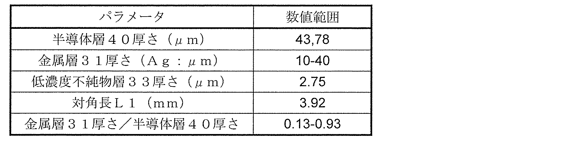
図3Aに示すように、金属層31を厚くするにつれて、オン抵抗が低くなっていく。
スマートホンやタブレットの充放電回路として、本開示の半導体装置が適用される場合、充電時間短縮や急速充電実現の制約から、オン抵抗は、20V耐圧仕様として、2.2~2.4mΩ以下が求められる。
図3Aより、オン抵抗が2.4mΩ以下を満たす金属層31の厚さは、20μm以上であることが必要となる。
図3Bは、比較例2に係る半導体装置における、半導体層40の厚さに対する金属層31の厚さの割合(以下、金属層31厚さ/半導体層40厚さ、と記す場合がある)、オン抵抗、および反り量の関係を示すグラフである。比較例2に係る半導体装置は、図1Aおよび図1Bに示された半導体装置1に対して、接着層39および支持体30が形成されていない構成を有している。比較例2に係る半導体装置として、金属層31の厚さを10μm~40μmの範囲で変化させ、かつ、半導体層40の厚さを28~93μmの範囲で変化させた場合のオン抵抗および半導体基板32および金属層31の積層体の反り量を測定した。上記反り量については、ベアチップの状態のサンプルを、リフロー工程を模した最高温度250℃の熱負荷サイクル下に置き、モアレ法によりベアチップの形状を測定し、測定された反り量の最大値を記録した。
表2に、比較例2に係る半導体装置の各パラメータを示す。
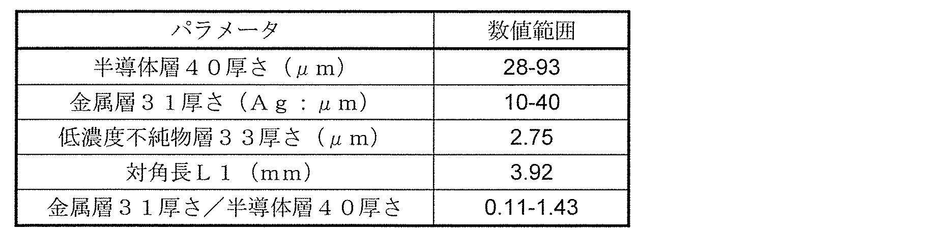
図3Bに示すように、金属層31厚さ/半導体層40厚さを大きくするにつれて、オン抵抗が低くなっていく。一方、金属層31厚さ/半導体層40厚さを大きくするにつれて、反り量が増加していく。
図3Bより、オン抵抗が2.4mΩ以下を満たす金属層31厚さ/半導体層40厚さは、0.27よりも大きいことが要求される。しかしながら、金属層31厚さ/半導体層40厚さは、0.27よりも大きくなると、反り量が20μm以上となる。反り量が大きくなるにつれ、実装基板へのフェイスダウン実装の際、安定した実装が困難となり、不具合が発生する。例えば、(1)半導体装置上の電極と実装基板上の電極との間の半田接合が不完全となる、(2)当該半田内でのボイドが発生する、(3)電極からの半田はみ出しによる電極間ショートが発生する、などの不具合が発生する。
つまり、比較例1および2に係る半導体装置の場合、オン抵抗を、充放電回路として必要な2.4mΩ以下を満たすためには、(1)金属層31の厚さは20μm以上、かつ、(2)金属層31厚さ/半導体層40厚さが0.27よりも大きいこと、が必要であるが、上記(1)および(2)を満たす場合、反り量が20μm以上となるといった問題が発生する。
[3.半導体装置のオン抵抗の低減および反りの低減を両立する構造]
上述した比較例1および2に係る半導体装置に対して、本実施の形態に係る半導体装置1は、金属層31の半導体基板32と反対側の主面全面に接して接着層39が形成され、接着層39の金属層31と反対側の主面全面に接して、セラミック材料からなる支持体30が形成されている。
上述した比較例1および2に係る半導体装置に対して、本実施の形態に係る半導体装置1は、金属層31の半導体基板32と反対側の主面全面に接して接着層39が形成され、接着層39の金属層31と反対側の主面全面に接して、セラミック材料からなる支持体30が形成されている。
セラミック材料からなる支持体30の応力発生の主要因である熱膨張係数およびヤング率などの物理定数は、金属材料からなる金属層31の上記物理定数よりも、半導体基板32の上記物理定数に近い値を有する。つまり、半導体基板32と金属層31との接合により発生する熱膨張応力を打ち消す方向の熱膨張応力が、支持体30と金属層31との接合により発生する。これにより、金属層31の対向する主面において、熱膨張応力のバランスがとれるため、金属層31および半導体層40の積層体の反りを抑制できる。
これに対して、特許文献1に係る半導体装置では、金属層の半導体基板と反対側の主面に接して導電層が形成されている。導電層の上記物理定数は、半導体基板の上記物理定数よりも金属層の上記物理定数に近い値を有する。このため、特許文献1に係る半導体装置では、半導体基板と金属層との接合により発生する応力を打ち消す方向の応力は、導電層と金属層との接合により発生しない。
また、本実施の形態に係る半導体装置1において、厚さ20μm以上であって、かつ、半導体層40に対する厚さの割合が0.27より大きい金属層31にかかる熱膨張応力を抑制するための支持体30としては、特許文献2に開示された絶縁被膜(塗布型の有機材料、有機系のテープ、または無機系酸化物薄膜)のような薄膜系の材料では不十分である。これに対して、厚さ20μm以上であって、かつ、半導体層40に対する厚さの割合が0.27より大きい金属層31にかかる熱膨張応力を抑制するための支持体30として、熱膨張係数およびヤング率が比較的半導体層40のそれに近いセラミック材料の支持体30を金属層31に直接貼り付けることは、現実的に困難である。よって、本実施の形態に係る半導体装置1では、金属層31と支持体30との間に、接着層39を介在させる構成としている。
これにより、厚さ20μm以上であって、かつ、半導体層40に対する厚さの割合が0.27より大きい金属層31にかかる熱膨張応力を抑制すべく、金属層31の半導体基板32と反対側に、接着層39およびセラミック材料からなる支持体30を形成することにより、オン抵抗の低減と半導体装置1の反りの抑制とを両立させたチップサイズパッケージ型の半導体装置1を提供することが可能となる。
なお、支持体30のセラミック材料は、例えば、シリコンである。これにより、窒化シリコンおよび酸化シリコンと比較しても、半導体装置をダイシングにより個片化する場合の切削加工性が向上する。また、窒化シリコンおよび酸化シリコンよりも材料入手が容易であり、また、低コストである。
また、金属層31の金属材料は、例えば、銀(Ag)である。これにより、金属材料として一般に用いられる銅(Cu)などと比較して、オン抵抗を効果的に低減することが可能となる。
なお、本実施の形態に係る半導体装置1において、金属層31は、半導体層40より厚くてもよい。これにより、オン抵抗のさらなる低減に貢献できる。
また、支持体30は、半導体層40より薄くてもよい。本実施の形態に係る半導体装置1の構成では、金属層31と支持体30との間の接着層39が介在するため、支持体30が半導体層40より薄い場合であっても、半導体基板32および金属層31の反り量低減に貢献できる。
また、接着層39は、導電性接着剤であってもよく、例えば、導電性DAFが挙げられる。また、導電性接着剤の材料としては、例えば、銀ペーストが挙げられる。これにより、オン抵抗のさらなる低減に貢献できる。
[4.半導体装置を構成する各層の厚さの最適化]
ここで、本実施の形態に係る半導体装置1のオン抵抗および反りを低減するための各層の厚さを最適化するプロセスについて説明する。
ここで、本実施の形態に係る半導体装置1のオン抵抗および反りを低減するための各層の厚さを最適化するプロセスについて説明する。
まず、物理定数の異なる多層を貼り合わせた場合に発生する反り量の理論式(多層ばり理論により導出された式)を、半導体層40、金属層31、接着層39、および支持体30の4層から構成される、本実施の形態に係る半導体装置1に適用する(ステップS10)。
次に、上記理論式に基づいて導出される本実施の形態に係る半導体装置1の反り量δが有限要素法を用いて構築された反り計算シミュレータでの計算値に合うように上記理論式をフィッティングする(ステップS20)。
最後に、上記理論式および反り計算シミュレータにより導出された実効的な反り量δeの算出式より、本実施の形態に係る半導体装置1の反り量δeが20μm以下および40μm以下となる場合の、接着層39および支持体30の厚さを導出する(ステップS30)。
まず、上記ステップS10について説明する。
図4Aは、多層体に発生する反り量を導出するための基本モデルを表す図である。図4Aに示すように、(熱膨張係数α1、ヤング率E1)および厚さt1を有する第1層、(熱膨張係数α2、ヤング率E2)および厚さt2を有する第2層、(熱膨張係数α3、ヤング率E3)および厚さt3を有する第3層、ならびに、(熱膨張係数α4、ヤング率E4)および厚さt4を有する第4層が、y軸負方向に向けて、この順で接合されている。なお、y軸方向からみた各層の長さLおよび幅(奥行き)bは、4層とも同じと仮定する。
図4Bは、多層体に発生する反り量δを説明する側面概略図である。同図に示すように、多層体に発生する応力により、多層体のx軸正方向の端部が、水平位置からy軸負方向にシフトする量を反り量δと定義する。
ここで、非特許文献1(尾田十八、「多層ばり理論によるプリント基板の応力・変形解析」、機論A編、pp.1777-1782、1993年)に記載された多層ばり理論に基づき、図4Aに示された多層体モデルに発生する反り量δは、以下の式1で表される。また、式1のRは、式2で表される。


式1および式2より、反り量δは、各層の厚さtn(n=1~4)の関数として表すことができ、当該関数を決定する他のパラメータが、各層の長さL、変化温度ΔT、各層の(αn、En)(n=1~4)である。
表3に、上記式1および式2を用いて求めた反り量δの一例を示す。また、表4に、表3の反り量δを求めた際に使用した他のパラメータを示す。

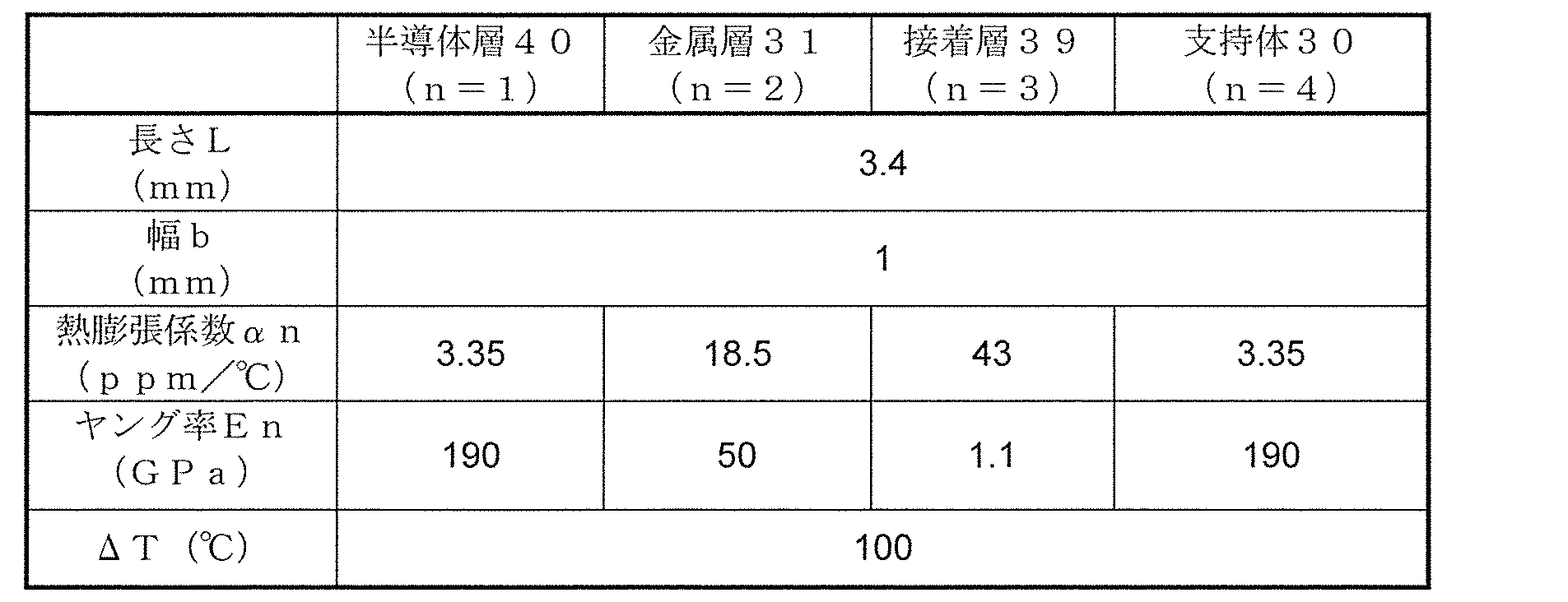
なお、表4において、幅bを1mmとしているが、これは、反り量δの計算に関して、幅bは分母および分子の双方に現れて相殺されるため、任意の値でよいことに起因するものである。
次に、上記ステップS20について説明する。ステップS20では、上記式1および式2に基づいて導出された反り量δが反り計算シミュレータでの計算値δsに合うように上記式1および式2をフィッティングする。なお、このフィッティングに用いた反り計算シミュレータは、有限要素法解析を用いた構造解析ソフトウェア(ANSYS社製)を、必要量の反り実測データを用いてカスタマイズしたものである。
上記反り計算シミュレータに、表3に示された各層の厚さt1~t4、表4に示された各パラメータを代入して得られた反り量の計算値δsを用いて、式1および式2により算出した理論的な反り量δを補正することが可能となる。具体的には、反り量δと反り量δsとの比をβ(=δs/δ)とすると、反り量δを反り計算シミュレータ算出値にフィッティングされた実効的な反り量δeへと変換できる。つまり、実効的な反り量δeは、フィッティング係数βを用いて、以下の式3で表される。
表3の各データにおいて、最適なフィッティング係数βは、0.67であった。
次に、上記ステップS30について説明する。式3に示された実効的な反り量δeの算出式(以降、実効値算出式と呼ぶ)により、本実施の形態に係る半導体装置1の反り量が(1)20μm以下、および、(2)40μm以下となる場合の、接着層39および支持体30の厚さを導出する。
図5は、実効値算出式を用いて算出した、接着層39の厚さ、および、支持体30の厚さに対する反り量δeの変化を表すグラフである。同図には、半導体層40の厚さを20μm、および、金属層31の厚さを30μmと固定し、接着層39の厚さを0μm、30μm、および50μmと変化させた場合の、支持体30の厚さと反り量δeとの関係が示されている。なお、その他のパラメータは、表4に示された値となっている。
図5のグラフより、まず、反り量δeを20μm以下にする接着層39と支持体30との関係を把握する。図5より、以下のことが解る。
(1)接着層39が厚い方が、反り量δeが0となる支持体30の厚さが小さい。つまり、接着層39の存在で支持体30の必要量が少なくなる。
(2)支持体30を厚くすると、一旦逆反りになる(反り量δeが負値をとる)が、さらに厚くすると0に近づく。逆反りにおける反り量δeの極小点は10μm程度であり、20μm以上にはならない。よって、接着層39および支持体30の厚さの条件を出す場合には、順反りを20μm以下にする条件を出せばよい。
上述した、接着層39および支持体30の厚さの条件出しにおいて、本実施の形態に係る半導体装置1は、異なる物理定数および異なる厚さを有する4つの層を有するため、検討対象のパラメータが多い。そこで、以下の方針により、接着層39および支持体30の厚さを算出する。
(1)主たるパラメータは、4つの層の各厚さ、および、反り量δeである。反り量δeの規格値を、第1規格値20μm、および、第2規格値40μmとする。
(2)本実施の形態に係る半導体装置1の特徴は、半導体層40および金属層31で発生する反りを抑制するために、接着層39および支持体30が配置されていることなので、反り量δeの規格値を満足する支持体30の厚さを、接着層39の厚さに依存する形式で規定する。つまり、使用する接着層39の厚さに応じて、支持体30の厚さを決定できる関数を導出する。
図6Aは、実効値算出式を用いて算出した、半導体層40の厚さを固定した場合((a)は半導体層40の厚さ10μm、(b)は半導体層40の厚さ80μm)の、反り量δeを20μmにするための、金属層31、接着層39および支持体30の厚さの関係を表すグラフである。また、図6Bは、実効値算出式を用いて算出した、金属層31の厚さを固定した場合((a)は金属層31の厚さ20μm、(b)は金属層31の厚さ70μm)の、反り量δeを20μmにするための、半導体層40、接着層39および支持体30の厚さの関係を表すグラフである。
図6Aの(a)および(b)に示すようなグラフを、半導体層40の厚さ20μm、40μm、60μmの場合においても、また、図6Bの(a)および(b)に示すようなグラフを、金属層31の厚さ40μm、50μm、60μmの場合においても実効値算出式を用いて取得する。このようにして取得されたグラフより、反り量δeを20μmにする接着層39の厚さ毎の支持体30の厚さを抽出する。このとき、半導体層40の厚さおよび金属層31の厚さの変化により、反り量δeを20μmにする接着層39の厚さ毎の支持体30の厚さは変化するが、半導体層40の厚さおよび金属層31の厚さが変化するなかで、接着層39の厚さ毎の支持体30の厚さの最大値を抽出する。同様の抽出プロセスを、反り量δeを40μmにする接着層39の厚さ毎の支持体30の厚さについても適用する。
表5に、この抽出プロセスにより取得された接着層39の厚さ毎の支持体30の厚さの組み合わせを示す。また、表6に、表5の反り量δeを求めた際に使用した他のパラメータを示す。
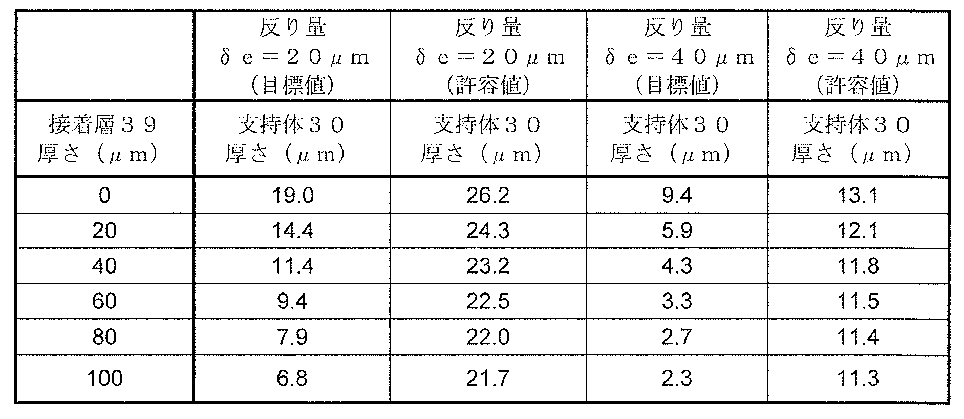

なお、反り量δe規格値である20μmおよび40μmを目標値として設定して、接着層39の厚さに対する支持体30の厚さの関係を抽出する場合には、表6に示されたパラメータのうち目標値を用い、反り量δe規格値である20μmおよび40μmを許容値として設定して、接着層39の厚さに対する支持体30の厚さの関係を抽出する場合には、表6に示されたパラメータのうち最大値を用いた。
図7は、実施の形態1に係る半導体装置1において、反り量20μmおよび40μmにするための接着層39の厚さに対する支持体30の厚さの関係を規定したグラフである。同図には、表5に示された抽出データがプロットされている。同図に示されたグラフより、(1)反り量δeを20μm(目標値)にする接着層39の厚さに対する支持体30の厚さの関係を表す近似式、(2)反り量δeを20μm(許容値)にする接着層39の厚さに対する支持体30の厚さの関係を表す近似式、(3)反り量δeを40μm(目標値)にする接着層39の厚さに対する支持体30の厚さの関係を表す近似式、(4)反り量δeを40μm(許容値)にする接着層39の厚さに対する支持体30の厚さの関係を表す近似式、が得られる。これらの近似式より、半導体装置1の反り量を抑制する接着層39の厚さに対する支持体30の厚さの関係は、式4~式7で表される。
(1)接着層39の厚さをt3(μm)とし、支持体30の厚さをt4(μm)とした場合、反り量δeを20μm以下とする接着層39の厚さに対する支持体30の厚さは、以下の式4で表される。
これにより、金属層31の厚さが20μm、かつ、金属層31厚さ/半導体層40厚さが0.27よりも大きい半導体装置1において、各層の長さLが3.4mm以下であり、接着層39の熱膨張係数α3が1.1(ppm/℃)以下であり、接着層39のヤング率E3が50(GPa)以下であるという条件において、半導体装置1の反り量を20μm以下とすることが可能となる。
(2)接着層39の厚さをt3(μm)とし、支持体30の厚さをt4(μm)とした場合、反り量δeを20μm以下とする接着層39の厚さに対する支持体30の厚さは、以下の式5で表される。
これにより、金属層31の厚さが20μm、かつ、金属層31厚さ/半導体層40厚さが0.27よりも大きい半導体装置1において、各層の長さLが4.0mm以下であり、接着層39の熱膨張係数α3が5.0(ppm/℃)以下であり、接着層39のヤング率E3が100(GPa)以下であるという条件において、半導体装置1の反り量を20μm以下とすることが可能となる。
(3)接着層39の厚さをt3(μm)とし、支持体30の厚さをt4(μm)とした場合、反り量δeを40μm以下とする接着層39の厚さに対する支持体30の厚さは、以下の式6で表される。
これにより、金属層31の厚さが20μm、かつ、金属層31厚さ/半導体層40厚さが0.27よりも大きい半導体装置1において、各層の長さLが3.4mm以下であり、接着層39の熱膨張係数α3が1.1(ppm/℃)以下であり、接着層39のヤング率E3が50(GPa)以下であるという条件において、半導体装置1の反り量を40μm以下とすることが可能となる。
(4)接着層39の厚さをt3(μm)とし、支持体30の厚さをt4(μm)とした場合、反り量δeを40μm以下とする接着層39の厚さに対する支持体30の厚さは、以下の式7で表される。
これにより、金属層31の厚さが20μm、かつ、金属層31厚さ/半導体層40厚さが0.27よりも大きい半導体装置1において、各層の長さLが4.0mm以下であり、接着層39の熱膨張係数α3が5.0(ppm/℃)以下であり、接着層39のヤング率E3が100(GPa)以下であるという条件において、半導体装置1の反り量を40μm以下とすることが可能となる。
[5.変形例に係る半導体装置の構造]
図8Aは、実施の形態1の変形例1に係る半導体装置1Aの断面図である。また、図8Bは、実施の形態1の変形例1に係る半導体装置1Aの電極構成の一例を示す上面図である。図8Aの断面図は、図8BのVIIIA-VIIIAにおける切断面を見た図である。図8Aに示すように、半導体装置1Aは、半導体基板32と、低濃度不純物層33と、金属層31と、接着層39と、支持体30と、トランジスタ10と、トランジスタ20と、を有する。図8Bに示すように、半導体装置1Aは、半導体基板32を平面視した場合、2つの第1のソース電極11、2つの第2のソース電極21、1つの第1のゲート電極19、および、1つの第2のゲート電極29を有している。トランジスタ10の上面には、トランジスタ10とトランジスタ20とが対向する方向と垂直な方向に沿って、第1のソース電極11、第1のゲート電極19、および第1のソース電極11がこの順に形成されている。また、トランジスタ20の上面には、トランジスタ10とトランジスタ20とが対向する方向と垂直な方向に沿って、第2のソース電極21、第1のゲート電極29、および第1のソース電極21がこの順に形成されている。なお、1つのトランジスタを構成するソース電極およびゲート電極の個数および配置関係は、図8Bに示されたものに限定されない。
図8Aは、実施の形態1の変形例1に係る半導体装置1Aの断面図である。また、図8Bは、実施の形態1の変形例1に係る半導体装置1Aの電極構成の一例を示す上面図である。図8Aの断面図は、図8BのVIIIA-VIIIAにおける切断面を見た図である。図8Aに示すように、半導体装置1Aは、半導体基板32と、低濃度不純物層33と、金属層31と、接着層39と、支持体30と、トランジスタ10と、トランジスタ20と、を有する。図8Bに示すように、半導体装置1Aは、半導体基板32を平面視した場合、2つの第1のソース電極11、2つの第2のソース電極21、1つの第1のゲート電極19、および、1つの第2のゲート電極29を有している。トランジスタ10の上面には、トランジスタ10とトランジスタ20とが対向する方向と垂直な方向に沿って、第1のソース電極11、第1のゲート電極19、および第1のソース電極11がこの順に形成されている。また、トランジスタ20の上面には、トランジスタ10とトランジスタ20とが対向する方向と垂直な方向に沿って、第2のソース電極21、第1のゲート電極29、および第1のソース電極21がこの順に形成されている。なお、1つのトランジスタを構成するソース電極およびゲート電極の個数および配置関係は、図8Bに示されたものに限定されない。
本変形例に係る半導体装置1Aは、実施の形態1に係る半導体装置1と比較して、トランジスタ10および20の境界に、切り込み部61が形成されている点のみが構成として異なる。以下、本変形例に係る半導体装置1Aについて、実施の形態1に係る半導体装置1と同じ構成については説明を省略し、異なる構成を中心に説明する。
図8Aおよび図8Bに示すように、本変形例に係る半導体装置1Aでは、トランジスタ10の第1の領域と、トランジスタ20の第2の領域との間の境界に、半導体装置1Aの上面側から下面側に向けて切り込み部61が形成されている。また、切り込み部61は、低濃度不純物層33まで形成されている。なお、本変形例に係る半導体装置1Aの切り込み部61の最下端は、半導体基板32の下面よりも半導体装置1Aの上面側に位置している。
これにより、半導体基板32と低濃度不純物層33との間の内部応力を緩和でき、半導体基板32と低濃度不純物層33との剥離を防止できる。また、切り込み部61が半導体基板32まで到達することにより、半導体基板32と金属層31との間の内部応力を緩和でき、半導体基板32と金属層31との剥離を防止できる。
図9は、実施の形態1の変形例2に係る半導体装置1Bの断面図である。なお、実施の形態1の変形例2に係る半導体装置1Bの電極構成の一例を示す上面図については、図8Bに示された半導体装置1Aの上面図と同様であるため省略する。
図9に示すように、半導体装置1Bは、半導体基板32と、低濃度不純物層33と、金属層31と、接着層39と、支持体30と、トランジスタ10と、トランジスタ20と、を有する。半導体装置1Bは、半導体基板32を平面視した場合、2つの第1のソース電極11、2つの第2のソース電極21、1つの第1のゲート電極19、および、1つの第2のゲート電極29を有している。トランジスタ10の上面には、トランジスタ10とトランジスタ20とが対向する方向と垂直な方向に沿って、第1のソース電極11、第1のゲート電極19、および第1のソース電極11がこの順に形成されている。また、トランジスタ20の上面には、トランジスタ10とトランジスタ20とが対向する方向と垂直な方向に沿って、第2のソース電極21、第1のゲート電極29、および第1のソース電極21がこの順に形成されている。なお、1つのトランジスタを構成するソース電極およびゲート電極の個数および配置関係は、図8Bに示されたものに限定されない。
本変形例に係る半導体装置1Bは、実施の形態1に係る半導体装置1と比較して、トランジスタ10および20の境界に切り込み部62が形成されている点のみが構成として異なる。以下、本変形例に係る半導体装置1Bについて、実施の形態1に係る半導体装置1と同じ構成については説明を省略し、異なる構成を中心に説明する。
図9に示すように、本変形例に係る半導体装置1Bでは、トランジスタ10の第1の領域と、トランジスタ20の第2の領域との間の境界に、半導体装置1Bの上面側から下面側に向けて切り込み部62が形成されている。また、切り込み部62は、金属層31まで形成されている。なお、本変形例に係る半導体装置1Bの切り込み部62の最下端は、金属層31の上面と下面との間に位置している。
これにより、半導体基板32と金属層31との間の内部応力を緩和でき、半導体基板32と金属層31との剥離を防止できる。さらに、金属層31と接着層39および支持体30との間の内部応力を緩和でき、金属層31と支持体30との間における剥離を防止できる。
[6.半導体装置の製造方法]
実施の形態1に係る半導体装置1の製造方法について、図10A~10C、図11A~11B、図12A~12B、図13および図14を参照しながら説明する。ここでは「縦型」MOSFETを例にとって説明するが、他に、ダイオード、「縦型」のバイポーラトランジスタ等においても同様の効果が得られることは言うまでもない。
実施の形態1に係る半導体装置1の製造方法について、図10A~10C、図11A~11B、図12A~12B、図13および図14を参照しながら説明する。ここでは「縦型」MOSFETを例にとって説明するが、他に、ダイオード、「縦型」のバイポーラトランジスタ等においても同様の効果が得られることは言うまでもない。
図10Aは、実施の形態1に係る半導体装置1の製造方法の第1工程を示す断面図である。図10Bは、実施の形態1に係る半導体装置1の製造方法の第2工程を示す断面図である。図10Cは、実施の形態1に係る半導体装置の製造方法の第3工程を示す断面図である。
まず、図10Aに示すように、半導体基板32Aの一主面上に低濃度不純物層33を形成し、さらに低濃度不純物層33の表面領域に素子領域を形成する。次に、素子領域上の所定箇所にAlまたはCu等の金属を主材料とする電極(第1のソース電極、第2のソース電極)を形成する。
次に、図10Bに示すように、半導体基板32Aの一主面側に仮接着剤37を塗布する。このとき、電極や素子領域などの凹凸よりも仮接着剤37を厚くすることが望ましい。さらに、仮接着剤37の上にガラス基板36をのせて押圧することで接着する。このとき、ガラス基板36と仮接着剤37との間に気泡が入らないようにするため、真空チャンバー内で接着することが望ましい。
次に、図10Cに示すように、求められる電気特性(オン抵抗)を実現できるように、半導体基板32Aの一主面と反対側の裏面を、半導体基板32Aの厚さが所望の厚さ(好ましくは50μm以下)にまでバックグラインドし、所望の厚さの半導体基板32を形成する。さらにCMP等の鏡面処理をしておくことが望ましい。
図11Aは、実施の形態1に係る半導体装置1の製造方法の第4工程を示す断面図である。図11Bは、実施の形態1に係る半導体装置1の製造方法の第5工程を示す断面図である。
次に、図11Aに示すように、半導体基板32の一主面と反対側の裏面上に、金属層31を形成する。具体的な方法としては、半導体基板32とオーミックコンタクトをとるように蒸着法を用いて半導体基板32の裏面全体に第1金属層31Aを形成する。ここで、第1金属層31Aとして、例えば、半導体基板32の裏面に近い側から順にTiおよびNiを積層する。
次に、第1金属層31A上に、第2金属層31Bを形成する。具体的には、電解めっき法を用いて形成する。ここで、第2金属層31Bとしては、主にAg、Au、Cuなどを用いるのが良い。以降の説明では、第1金属層31Aと第2金属層31Bとを合わせて金属層31と呼ぶ。
次に、図11Bに示すように、金属層31上に接着剤を塗布し、接着層39を形成する。このとき、金属層31の表面凹凸よりも接着層39を厚くすることが望ましい。さらに、接着層39の上に支持体30をのせて押圧することで接着する。このとき、支持体30と接着層39との間に気泡が入らないようにするため、真空チャンバー内で接着することが望ましい。
接着層39を形成する接着剤としては、エポキシ樹脂、フェノール樹脂などの熱硬化型樹脂を用いる。また、支持体30として、シリコンなどの材料のほかに、石英、サファイヤ、ほうけい酸ガラス、ソーダ石灰ガラスなど、紫外線に対して透明な材料を用いる場合は、接着剤として、エポキシアクリレート、アクリル酸アクリレート、ウレタンアクリレートなどの紫外線硬化型樹脂を用いることもできる。
次に、上記接着剤を硬化させる工程について説明する。接着剤として熱硬化型樹脂を用いる場合の工程としては、貼り合わせを行ったウェハを、例えば、150℃程度の恒温炉に入れて1~2時間加熱する。加熱により上記接着剤を硬化させ、支持体30と金属層31との間を強く接着させる。
また、上記接着剤に紫外線硬化型樹脂を用いる場合には、高圧水銀ランプなどの紫外線発生装置を用いて貼り合わせを行ったウェハの支持体30側の面に対して、紫外線を照射する。照射する光量は例えば、300~2000mJ/cm2とする。
図12Aは、実施の形態1に係る半導体装置1の製造方法の第6工程を示す断面図である。図12Bは、実施の形態1に係る半導体装置1の製造方法の第7工程を示す断面図である。
次に、図12Aに示すように、支持体30の表面、およびリングフレーム50にダイシングテープ38を貼付けて、リングフレーム50へのマウントを行う。
次に、仮接着剤37とガラス基板36とを除去する。具体的には、図12Aに示すように、仮接着剤37のガラス基板36との境界面付近にレーザー光70を照射することで、ガラス基板36に接している部分の仮接着剤37を改質させて、半導体基板32からなるウェハからガラス基板36を除去する。その後、図12Bに示すように、仮接着剤37を剥離除去する。
図13は、実施の形態1に係る半導体装置1の製造方法の第8工程を示す断面図である。
最後に、図13に示すように、例えば、ダイシングソー等のダイシングブレード80を用いて、半導体基板32、低濃度不純物層33、金属層31、接着層39、および支持体30をダイシングして複数の半導体基板1へ個片化する。
金属層31を含む半導体基板32のダイシングの際は、切削した金属がブレードに付着して目詰まり状態となり切削能力を維持できないという課題がある。さらに、シリコンからなる半導体基板32を薄くしていくと、ブレードへの切削負荷が減少しブレードの磨耗が遅くなり前述の目詰まりを解消しにくくなるという悪循環に至り、さらに切削能力の維持が難しくなることが想定される。これに対して、本実施の形態に係る半導体装置1では、支持体30としてシリコンを用いる。シリコンは、ブレードに適度な負荷を与えブレードの磨耗を促進する材質であるため、上記の目詰まり課題を改善できる。
また、比較例1および2のような従来の構造では、半導体装置の片側最表面が金属層となっているため、ダイシング加工で金属層を切削する際にブレードで金属層が引き伸ばされ大きなバリが発生する。
これに対して、本実施の形態に係る半導体装置1の製造工程では、金属層31が半導体基板32および支持体30に挟まれている構造であるため、最表面に金属層31のような延性材料がない状態となるため、切削端面にバリが発生しにくい、という効果を奏する。
図14は、実施の形態1に係る半導体装置の製造方法の第9工程を示す断面図である。さらに別の一例として、図14に示すように、最後のダイシング工程の際に、複数のトランジスタ間にダイシングブレード81を用いて切り込み64を入れる。これにより、半導体基板32とその上に形成された素子領域や電極による内部応力を緩和することができ、半導体基板32と金属層31との間の剥離を防止できる。図14の工程は、図10A~10C、図11A~11B、図12A~12Bに示した製造工程の後、実行されてもよく、図14の工程の後に、図13に示すダイシング工程により個別の半導体装置1へと分離される。図14に示すように、半導体装置1に形成された複数のトランジスタ間にダイシングブレード81によって切り込み64が形成される。
以上、本開示の1つまたは複数の態様に係る半導体装置について、実施の形態に基づいて説明したが、本開示は、この実施の形態に限定されるものではない。本開示の趣旨を逸脱しない限り、当業者が思いつく各種変形を本実施の形態に施したものや、異なる実施の形態における構成要素を組み合わせて構築される形態も、本開示の1つまたは複数の態様の範囲内に含まれてもよい。
本願発明に係る半導体装置は、CSP型の半導体装置として、双方向トランジスタ、単方向トランジスタ、ダイオードなどの各種の半導体装置に広く利用できる。
1、1A、1B 半導体装置
2 制御IC
3 電池
4 負荷
10 トランジスタ(第1の縦型MOSトランジスタ)
11 第1のソース電極
12、22 第1の部分
13、23 第2の部分
14 第1のソース領域
15 第1のゲート導体
16 第1のゲート絶縁膜
18 第1のボディ領域
19 第1のゲート電極
20 トランジスタ(第2の縦型MOSトランジスタ)
21 第2のソース電極
24 第2のソース領域
25 第2のゲート導体
26 第2のゲート絶縁膜
28 第2のボディ領域
29 第2のゲート電極
30 支持体
31 金属層
31A 第1金属層
31B 第2金属層
32、32A 半導体基板
33 低濃度不純物層
34 層間絶縁層
35 パッシベーション層
36 ガラス基板
37 仮接着剤
38 ダイシングテープ
39 接着層
40 半導体層
50 リングフレーム
61、62 切り込み部
63、64 切り込み
70 レーザー光
80、81 ダイシングブレード
Claims (12)
- フェイスダウン実装が可能なチップサイズパッケージ型の半導体装置であって、
第1導電型の不純物を含み、シリコンからなる半導体基板と、
前記半導体基板の上面に接して形成され、前記半導体基板の前記第1導電型の不純物の濃度より低い濃度の前記第1導電型の不純物を含む低濃度不純物層と、
前記半導体基板の下面全面に接して形成され、厚さが20μm以上の金属材料のみで構成された金属層と、
前記低濃度不純物層内の第1の領域に形成された第1の縦型MOSトランジスタと、
前記第1の領域と前記半導体基板の上面に沿った方向で隣接する、前記低濃度不純物層内の第2の領域に形成された第2の縦型MOSトランジスタと、を備え、
前記第1の縦型MOSトランジスタは、前記低濃度不純物層の上面に形成された第1のソース電極および第1のゲート電極を有し、
前記第2の縦型MOSトランジスタは、前記低濃度不純物層の上面に形成された第2のソース電極および第2のゲート電極を有し、
前記半導体基板は、前記第1の縦型MOSトランジスタの第1のドレイン領域および前記第2の縦型MOSトランジスタの第2のドレイン領域を共通化したドレイン領域として機能し、
前記第1のソース電極と前記第2のソース電極との間を、前記第1のドレイン領域、前記金属層、および前記第2のドレイン領域を経由して流れる双方向経路を主電流経路とし、
前記半導体基板と前記低濃度不純物層とを含む半導体層に対する前記金属層の厚さの割合は0.27より大きく、
前記半導体装置は、さらに、
前記金属層の下面全面に、接着層のみを介して接着された、セラミック材料からなる支持体を有する
半導体装置。 - 前記セラミック材料は、シリコンである
請求項1に記載の半導体装置。 - 前記金属材料は、銀である
請求項1または2に記載の半導体装置。 - 前記金属層の厚さは、前記半導体層の厚さより厚い
請求項3に記載の半導体装置。 - 前記支持体の厚さは、前記半導体層の厚さより薄い
請求項3に記載の半導体装置。 - 前記接着層の構成材料は、導電性材料である
請求項3に記載の半導体装置。 - 前記支持体の厚さをt4、前記接着層の厚さをt3とした場合、

請求項3に記載の半導体装置。 - 前記支持体の厚さをt4、前記接着層の厚さをt3とした場合、

請求項7に記載の半導体装置。 - 前記支持体の厚さをt4、前記接着層の厚さをt3とした場合、

請求項7に記載の半導体装置。 - 前記支持体の厚さをt4、前記接着層の厚さをt3とした場合、

請求項9に記載の半導体装置。 - 前記第1の領域と前記第2の領域との間の境界に、前記半導体装置の上面側から下面側に向けて切り込み部が形成されており、
前記切り込み部の最下端は、前記半導体基板の下面よりも前記上面側に位置する
請求項1に記載の半導体装置。 - 前記切り込み部の最下端は、前記金属層の上面と下面との間に位置する
請求項11に記載の半導体装置。
Priority Applications (5)
| Application Number | Priority Date | Filing Date | Title |
|---|---|---|---|
| CN202210609454.3A CN114975302A (zh) | 2016-12-27 | 2017-12-21 | 半导体装置 |
| JP2018559114A JP7042217B2 (ja) | 2016-12-27 | 2017-12-21 | 半導体装置 |
| CN201780080128.5A CN110114888B (zh) | 2016-12-27 | 2017-12-21 | 半导体装置 |
| US16/447,100 US10854744B2 (en) | 2016-12-27 | 2019-06-20 | Semiconductor device |
| US17/070,211 US11056589B2 (en) | 2016-12-27 | 2020-10-14 | Semiconductor device |
Applications Claiming Priority (2)
| Application Number | Priority Date | Filing Date | Title |
|---|---|---|---|
| US201662439343P | 2016-12-27 | 2016-12-27 | |
| US62/439343 | 2016-12-27 |
Related Child Applications (1)
| Application Number | Title | Priority Date | Filing Date |
|---|---|---|---|
| US16/447,100 Continuation US10854744B2 (en) | 2016-12-27 | 2019-06-20 | Semiconductor device |
Publications (1)
| Publication Number | Publication Date |
|---|---|
| WO2018123799A1 true WO2018123799A1 (ja) | 2018-07-05 |
Family
ID=62710538
Family Applications (1)
| Application Number | Title | Priority Date | Filing Date |
|---|---|---|---|
| PCT/JP2017/045908 WO2018123799A1 (ja) | 2016-12-27 | 2017-12-21 | 半導体装置 |
Country Status (5)
| Country | Link |
|---|---|
| US (2) | US10854744B2 (ja) |
| JP (1) | JP7042217B2 (ja) |
| CN (2) | CN110114888B (ja) |
| TW (1) | TW201830618A (ja) |
| WO (1) | WO2018123799A1 (ja) |
Cited By (12)
| Publication number | Priority date | Publication date | Assignee | Title |
|---|---|---|---|---|
| JP2020043164A (ja) * | 2018-09-07 | 2020-03-19 | 株式会社東芝 | 半導体装置 |
| WO2020129786A1 (ja) * | 2018-12-19 | 2020-06-25 | パナソニックセミコンダクターソリューションズ株式会社 | 半導体装置 |
| US10903359B2 (en) | 2018-06-19 | 2021-01-26 | Panasonic Semiconductor Solutions Co., Ltd. | Semiconductor device |
| US10930748B2 (en) | 2018-06-19 | 2021-02-23 | Panasonic Semiconductor Solutions Co., Ltd. | Semiconductor device |
| JP2021044287A (ja) * | 2019-09-06 | 2021-03-18 | 株式会社東芝 | 半導体装置およびその製造方法 |
| JPWO2022085765A1 (ja) * | 2020-10-23 | 2022-04-28 | ||
| JP7114824B1 (ja) * | 2021-09-17 | 2022-08-08 | ヌヴォトンテクノロジージャパン株式会社 | 半導体装置 |
| WO2022224889A1 (ja) * | 2021-04-22 | 2022-10-27 | 有限会社Mtec | 半導体素子の製造方法及び縦型mosfet素子 |
| JP7323735B1 (ja) * | 2022-03-22 | 2023-08-08 | ヌヴォトンテクノロジージャパン株式会社 | 製造方法および半導体装置 |
| WO2023162735A1 (ja) * | 2022-02-24 | 2023-08-31 | ヌヴォトンテクノロジージャパン株式会社 | 半導体装置 |
| WO2023181460A1 (ja) * | 2022-03-22 | 2023-09-28 | ヌヴォトンテクノロジージャパン株式会社 | 製造方法および半導体装置 |
| TWI838119B (zh) | 2022-02-24 | 2024-04-01 | 日商新唐科技日本股份有限公司 | 半導體裝置 |
Families Citing this family (6)
| Publication number | Priority date | Publication date | Assignee | Title |
|---|---|---|---|---|
| CN110114888B (zh) * | 2016-12-27 | 2022-06-21 | 新唐科技日本株式会社 | 半导体装置 |
| US11367619B2 (en) * | 2017-08-17 | 2022-06-21 | Semiconductor Components Industries, Llc | Semiconductor package electrical contacts and related methods |
| JP6573189B1 (ja) * | 2018-06-19 | 2019-09-11 | パナソニックIpマネジメント株式会社 | 半導体装置 |
| TWI712120B (zh) * | 2018-06-19 | 2020-12-01 | 日商松下半導體解決方案股份有限公司 | 半導體裝置 |
| WO2021079879A1 (ja) | 2019-10-21 | 2021-04-29 | ヌヴォトンテクノロジージャパン株式会社 | 半導体装置および個片化方法 |
| KR102606591B1 (ko) * | 2021-03-29 | 2023-11-29 | 누보톤 테크놀로지 재팬 가부시키가이샤 | 반도체 장치, 전지 보호 회로, 및, 파워 매니지먼트 회로 |
Citations (6)
| Publication number | Priority date | Publication date | Assignee | Title |
|---|---|---|---|---|
| JP2001127290A (ja) * | 1999-10-29 | 2001-05-11 | Nec Corp | 縦型電界効果トランジスタ及びその作製方法 |
| JP2004342718A (ja) * | 2003-05-14 | 2004-12-02 | Toshiba Corp | 半導体装置及びコンバータ |
| JP2007005657A (ja) * | 2005-06-24 | 2007-01-11 | Nec Electronics Corp | 半導体装置及び半導体装置の製造方法 |
| JP2008060105A (ja) * | 2006-08-29 | 2008-03-13 | Shindengen Electric Mfg Co Ltd | 半導体装置および該半導体装置の製造方法 |
| JP2015231033A (ja) * | 2014-06-06 | 2015-12-21 | ルネサスエレクトロニクス株式会社 | 半導体装置及び半導体装置の製造方法 |
| JP2016197737A (ja) * | 2016-06-29 | 2016-11-24 | 株式会社タムラ製作所 | 半導体素子及びその製造方法、並びに結晶積層構造体 |
Family Cites Families (23)
| Publication number | Priority date | Publication date | Assignee | Title |
|---|---|---|---|---|
| US6448624B1 (en) * | 1996-08-09 | 2002-09-10 | Denso Corporation | Semiconductor acceleration sensor |
| JP4164874B2 (ja) * | 2004-05-31 | 2008-10-15 | サンケン電気株式会社 | 半導体装置 |
| JP5124934B2 (ja) | 2005-02-04 | 2013-01-23 | ソニー株式会社 | 固体撮像素子及びその製造方法、撮像装置 |
| JP2010092895A (ja) | 2008-10-03 | 2010-04-22 | Sanyo Electric Co Ltd | 半導体装置及びその製造方法 |
| TW201015718A (en) | 2008-10-03 | 2010-04-16 | Sanyo Electric Co | Semiconductor device and method for manufacturing the same |
| US9257328B2 (en) * | 2008-11-26 | 2016-02-09 | Corning Incorporated | Glass-ceramic-based semiconductor-on-insulator structures and method for making the same |
| US8188484B2 (en) * | 2008-12-25 | 2012-05-29 | Rohm Co., Ltd. | Semiconductor device |
| JP4894910B2 (ja) * | 2009-01-15 | 2012-03-14 | 株式会社デンソー | 半導体装置の製造方法及び半導体装置並びにその半導体装置を内蔵する多層基板 |
| JP2010205761A (ja) | 2009-02-27 | 2010-09-16 | Sanyo Electric Co Ltd | 半導体装置およびその製造方法 |
| WO2011087994A2 (en) * | 2010-01-12 | 2011-07-21 | Maxpower Semiconductor Inc. | Devices, components and methods combining trench field plates with immobile electrostatic charge |
| JP2012182238A (ja) * | 2011-02-28 | 2012-09-20 | Panasonic Corp | 半導体装置 |
| JP2012182239A (ja) | 2011-02-28 | 2012-09-20 | Panasonic Corp | 半導体装置の製造方法 |
| US20130154049A1 (en) * | 2011-06-22 | 2013-06-20 | George IMTHURN | Integrated Circuits on Ceramic Wafers Using Layer Transfer Technology |
| ITMI20121134A1 (it) * | 2012-06-27 | 2013-12-28 | St Microelectronics Srl | Dispositivo elettronico flip chip e relativo metodo di produzione |
| JP6281897B2 (ja) * | 2013-10-30 | 2018-02-21 | ルネサスエレクトロニクス株式会社 | 半導体装置 |
| JP2016031953A (ja) * | 2014-07-25 | 2016-03-07 | 株式会社タムラ製作所 | 半導体素子及びその製造方法、半導体基板、並びに結晶積層構造体 |
| JP6356550B2 (ja) * | 2014-09-10 | 2018-07-11 | 三菱電機株式会社 | 半導体装置およびその製造方法 |
| JP6341822B2 (ja) * | 2014-09-26 | 2018-06-13 | 三菱電機株式会社 | 半導体装置 |
| JP2016086006A (ja) * | 2014-10-23 | 2016-05-19 | パナソニックIpマネジメント株式会社 | 半導体装置及びその製造方法 |
| JP6511695B2 (ja) | 2015-01-20 | 2019-05-15 | ローム株式会社 | 半導体装置およびその製造方法 |
| JP2016164962A (ja) | 2015-02-26 | 2016-09-08 | ルネサスエレクトロニクス株式会社 | 半導体チップおよび半導体装置並びに電池パック |
| CN110114888B (zh) * | 2016-12-27 | 2022-06-21 | 新唐科技日本株式会社 | 半导体装置 |
| JP6447946B1 (ja) | 2018-01-19 | 2019-01-09 | パナソニックIpマネジメント株式会社 | 半導体装置および半導体モジュール |
-
2017
- 2017-12-21 CN CN201780080128.5A patent/CN110114888B/zh active Active
- 2017-12-21 WO PCT/JP2017/045908 patent/WO2018123799A1/ja active Application Filing
- 2017-12-21 CN CN202210609454.3A patent/CN114975302A/zh active Pending
- 2017-12-21 JP JP2018559114A patent/JP7042217B2/ja active Active
- 2017-12-22 TW TW106145348A patent/TW201830618A/zh unknown
-
2019
- 2019-06-20 US US16/447,100 patent/US10854744B2/en active Active
-
2020
- 2020-10-14 US US17/070,211 patent/US11056589B2/en active Active
Patent Citations (6)
| Publication number | Priority date | Publication date | Assignee | Title |
|---|---|---|---|---|
| JP2001127290A (ja) * | 1999-10-29 | 2001-05-11 | Nec Corp | 縦型電界効果トランジスタ及びその作製方法 |
| JP2004342718A (ja) * | 2003-05-14 | 2004-12-02 | Toshiba Corp | 半導体装置及びコンバータ |
| JP2007005657A (ja) * | 2005-06-24 | 2007-01-11 | Nec Electronics Corp | 半導体装置及び半導体装置の製造方法 |
| JP2008060105A (ja) * | 2006-08-29 | 2008-03-13 | Shindengen Electric Mfg Co Ltd | 半導体装置および該半導体装置の製造方法 |
| JP2015231033A (ja) * | 2014-06-06 | 2015-12-21 | ルネサスエレクトロニクス株式会社 | 半導体装置及び半導体装置の製造方法 |
| JP2016197737A (ja) * | 2016-06-29 | 2016-11-24 | 株式会社タムラ製作所 | 半導体素子及びその製造方法、並びに結晶積層構造体 |
Cited By (35)
| Publication number | Priority date | Publication date | Assignee | Title |
|---|---|---|---|---|
| US10903359B2 (en) | 2018-06-19 | 2021-01-26 | Panasonic Semiconductor Solutions Co., Ltd. | Semiconductor device |
| US11107915B2 (en) | 2018-06-19 | 2021-08-31 | Nuvoton Technology Corporation Japan | Semiconductor device |
| US10930748B2 (en) | 2018-06-19 | 2021-02-23 | Panasonic Semiconductor Solutions Co., Ltd. | Semiconductor device |
| JP2020043164A (ja) * | 2018-09-07 | 2020-03-19 | 株式会社東芝 | 半導体装置 |
| JP7116640B2 (ja) | 2018-09-07 | 2022-08-10 | 株式会社東芝 | 半導体装置 |
| KR102308044B1 (ko) * | 2018-12-19 | 2021-10-01 | 누보톤 테크놀로지 재팬 가부시키가이샤 | 반도체 장치 |
| KR20210016094A (ko) * | 2018-12-19 | 2021-02-10 | 누보톤 테크놀로지 재팬 가부시키가이샤 | 반도체 장치 |
| JP2021005732A (ja) * | 2018-12-19 | 2021-01-14 | ヌヴォトンテクノロジージャパン株式会社 | 半導体装置および実装基板 |
| CN113314527A (zh) * | 2018-12-19 | 2021-08-27 | 新唐科技日本株式会社 | 半导体装置 |
| JP6775872B1 (ja) * | 2018-12-19 | 2020-10-28 | ヌヴォトンテクノロジージャパン株式会社 | 半導体装置 |
| KR102306576B1 (ko) | 2018-12-19 | 2021-09-29 | 누보톤 테크놀로지 재팬 가부시키가이샤 | 반도체 장치 |
| KR20200097357A (ko) * | 2018-12-19 | 2020-08-18 | 파나소닉 세미컨덕터 솔루션즈 가부시키가이샤 | 반도체 장치 |
| US11171234B2 (en) | 2018-12-19 | 2021-11-09 | Nuvoton Technology Corporation Japan | Semiconductor device |
| JP7038778B2 (ja) | 2018-12-19 | 2022-03-18 | ヌヴォトンテクノロジージャパン株式会社 | 半導体装置 |
| US11715795B2 (en) | 2018-12-19 | 2023-08-01 | Nuvoton Technology Corporation Japan | Semiconductor device |
| WO2020129786A1 (ja) * | 2018-12-19 | 2020-06-25 | パナソニックセミコンダクターソリューションズ株式会社 | 半導体装置 |
| JP2021044287A (ja) * | 2019-09-06 | 2021-03-18 | 株式会社東芝 | 半導体装置およびその製造方法 |
| JP7241649B2 (ja) | 2019-09-06 | 2023-03-17 | 株式会社東芝 | 半導体装置およびその製造方法 |
| WO2022085765A1 (ja) * | 2020-10-23 | 2022-04-28 | ヌヴォトンテクノロジージャパン株式会社 | 半導体装置 |
| CN115956297B (zh) * | 2020-10-23 | 2023-09-08 | 新唐科技日本株式会社 | 半导体装置 |
| US11735655B2 (en) | 2020-10-23 | 2023-08-22 | Nuvoton Technology Corporation Japan | Semiconductor device |
| JP7179236B2 (ja) | 2020-10-23 | 2022-11-28 | ヌヴォトンテクノロジージャパン株式会社 | 半導体装置 |
| JPWO2022085765A1 (ja) * | 2020-10-23 | 2022-04-28 | ||
| CN115956297A (zh) * | 2020-10-23 | 2023-04-11 | 新唐科技日本株式会社 | 半导体装置 |
| WO2022224889A1 (ja) * | 2021-04-22 | 2022-10-27 | 有限会社Mtec | 半導体素子の製造方法及び縦型mosfet素子 |
| WO2023042359A1 (ja) * | 2021-09-17 | 2023-03-23 | ヌヴォトンテクノロジージャパン株式会社 | 半導体装置 |
| JP7114824B1 (ja) * | 2021-09-17 | 2022-08-08 | ヌヴォトンテクノロジージャパン株式会社 | 半導体装置 |
| US11637176B2 (en) | 2021-09-17 | 2023-04-25 | Nuvoton Technology Corporation Japan | Semiconductor device |
| CN115152032B (zh) * | 2021-09-17 | 2023-03-14 | 新唐科技日本株式会社 | 半导体装置 |
| CN115152032A (zh) * | 2021-09-17 | 2022-10-04 | 新唐科技日本株式会社 | 半导体装置 |
| WO2023162735A1 (ja) * | 2022-02-24 | 2023-08-31 | ヌヴォトンテクノロジージャパン株式会社 | 半導体装置 |
| JP7393593B1 (ja) | 2022-02-24 | 2023-12-06 | ヌヴォトンテクノロジージャパン株式会社 | 半導体装置 |
| TWI838119B (zh) | 2022-02-24 | 2024-04-01 | 日商新唐科技日本股份有限公司 | 半導體裝置 |
| JP7323735B1 (ja) * | 2022-03-22 | 2023-08-08 | ヌヴォトンテクノロジージャパン株式会社 | 製造方法および半導体装置 |
| WO2023181460A1 (ja) * | 2022-03-22 | 2023-09-28 | ヌヴォトンテクノロジージャパン株式会社 | 製造方法および半導体装置 |
Also Published As
| Publication number | Publication date |
|---|---|
| CN114975302A (zh) | 2022-08-30 |
| CN110114888B (zh) | 2022-06-21 |
| US11056589B2 (en) | 2021-07-06 |
| US20210050444A1 (en) | 2021-02-18 |
| JPWO2018123799A1 (ja) | 2019-10-31 |
| US10854744B2 (en) | 2020-12-01 |
| US20190319126A1 (en) | 2019-10-17 |
| TW201830618A (zh) | 2018-08-16 |
| CN110114888A (zh) | 2019-08-09 |
| JP7042217B2 (ja) | 2022-03-25 |
Similar Documents
| Publication | Publication Date | Title |
|---|---|---|
| WO2018123799A1 (ja) | 半導体装置 | |
| US10395967B2 (en) | Method for manufacturing semiconductor device | |
| US7635635B2 (en) | Method for bonding a semiconductor substrate to a metal substrate | |
| US20110300651A1 (en) | Method for manufacturing light-emitting device | |
| US20180053737A1 (en) | Power semiconductor device | |
| US8907407B2 (en) | Semiconductor device covered by front electrode layer and back electrode layer | |
| JP2016086006A (ja) | 半導体装置及びその製造方法 | |
| US10068825B2 (en) | Semiconductor device | |
| US9224698B1 (en) | Semiconductor device | |
| CN110676165A (zh) | 半导体器件和制造半导体器件的方法 | |
| JP2019016738A (ja) | 半導体装置 | |
| JP2014049695A (ja) | 半導体装置及びその製造方法 | |
| US9520380B2 (en) | Wafer process for molded chip scale package (MCSP) with thick backside metallization | |
| TWI584431B (zh) | 超薄半導體元件封裝結構的製造方法 | |
| WO2019244384A1 (ja) | 半導体装置 | |
| US10700018B2 (en) | Reinforced semiconductor die and related methods | |
| WO2022224889A1 (ja) | 半導体素子の製造方法及び縦型mosfet素子 | |
| US11532618B2 (en) | Semiconductor device | |
| JP7392329B2 (ja) | 半導体装置 | |
| JP7059914B2 (ja) | 半導体モジュール | |
| WO2022114171A1 (ja) | 半導体素子の製造方法及び縦型mosfet素子 | |
| TWI540703B (zh) | 半導體元件及其製作方法 | |
| JP2011176206A (ja) | 半導体装置およびその製造方法 | |
| JP2005217012A (ja) | 半導体装置及びその製造方法 | |
| JP2010092894A (ja) | 半導体装置の製造方法 |
Legal Events
| Date | Code | Title | Description |
|---|---|---|---|
| 121 | Ep: the epo has been informed by wipo that ep was designated in this application |
Ref document number: 17886821 Country of ref document: EP Kind code of ref document: A1 |
|
| ENP | Entry into the national phase |
Ref document number: 2018559114 Country of ref document: JP Kind code of ref document: A |
|
| NENP | Non-entry into the national phase |
Ref country code: DE |
|
| 122 | Ep: pct application non-entry in european phase |
Ref document number: 17886821 Country of ref document: EP Kind code of ref document: A1 |