WO2023162735A1 - 半導体装置 - Google Patents
半導体装置 Download PDFInfo
- Publication number
- WO2023162735A1 WO2023162735A1 PCT/JP2023/004664 JP2023004664W WO2023162735A1 WO 2023162735 A1 WO2023162735 A1 WO 2023162735A1 JP 2023004664 W JP2023004664 W JP 2023004664W WO 2023162735 A1 WO2023162735 A1 WO 2023162735A1
- Authority
- WO
- WIPO (PCT)
- Prior art keywords
- gate
- gate trench
- low
- concentration impurity
- trench
- Prior art date
Links
- 239000004065 semiconductor Substances 0.000 title claims abstract description 140
- 239000012535 impurity Substances 0.000 claims abstract description 118
- 239000004020 conductor Substances 0.000 claims abstract description 52
- 230000005669 field effect Effects 0.000 claims abstract description 21
- 210000000746 body region Anatomy 0.000 claims description 45
- 239000000758 substrate Substances 0.000 claims description 33
- 238000000034 method Methods 0.000 claims description 5
- 239000010410 layer Substances 0.000 description 180
- 230000005684 electric field Effects 0.000 description 49
- 230000015556 catabolic process Effects 0.000 description 15
- 230000000052 comparative effect Effects 0.000 description 15
- 230000000694 effects Effects 0.000 description 13
- 239000011229 interlayer Substances 0.000 description 13
- 238000004519 manufacturing process Methods 0.000 description 11
- 229910052751 metal Inorganic materials 0.000 description 11
- 239000002184 metal Substances 0.000 description 11
- 230000009977 dual effect Effects 0.000 description 8
- 238000004088 simulation Methods 0.000 description 7
- 230000007423 decrease Effects 0.000 description 6
- 230000006866 deterioration Effects 0.000 description 5
- 239000007769 metal material Substances 0.000 description 5
- 238000002161 passivation Methods 0.000 description 5
- PXHVJJICTQNCMI-UHFFFAOYSA-N Nickel Chemical compound [Ni] PXHVJJICTQNCMI-UHFFFAOYSA-N 0.000 description 4
- KDLHZDBZIXYQEI-UHFFFAOYSA-N Palladium Chemical compound [Pd] KDLHZDBZIXYQEI-UHFFFAOYSA-N 0.000 description 4
- 239000000470 constituent Substances 0.000 description 4
- 239000010949 copper Substances 0.000 description 4
- PCHJSUWPFVWCPO-UHFFFAOYSA-N gold Chemical compound [Au] PCHJSUWPFVWCPO-UHFFFAOYSA-N 0.000 description 4
- 229910052737 gold Inorganic materials 0.000 description 4
- 239000010931 gold Substances 0.000 description 4
- RYGMFSIKBFXOCR-UHFFFAOYSA-N Copper Chemical compound [Cu] RYGMFSIKBFXOCR-UHFFFAOYSA-N 0.000 description 3
- BQCADISMDOOEFD-UHFFFAOYSA-N Silver Chemical compound [Ag] BQCADISMDOOEFD-UHFFFAOYSA-N 0.000 description 3
- 229910052802 copper Inorganic materials 0.000 description 3
- 238000010586 diagram Methods 0.000 description 3
- 238000005530 etching Methods 0.000 description 3
- 239000002784 hot electron Substances 0.000 description 3
- 230000002093 peripheral effect Effects 0.000 description 3
- 229910052709 silver Inorganic materials 0.000 description 3
- 239000004332 silver Substances 0.000 description 3
- RTAQQCXQSZGOHL-UHFFFAOYSA-N Titanium Chemical compound [Ti] RTAQQCXQSZGOHL-UHFFFAOYSA-N 0.000 description 2
- 229910052782 aluminium Inorganic materials 0.000 description 2
- XAGFODPZIPBFFR-UHFFFAOYSA-N aluminium Chemical compound [Al] XAGFODPZIPBFFR-UHFFFAOYSA-N 0.000 description 2
- 230000015572 biosynthetic process Effects 0.000 description 2
- 239000000203 mixture Substances 0.000 description 2
- 238000012986 modification Methods 0.000 description 2
- 230000004048 modification Effects 0.000 description 2
- 229910052759 nickel Inorganic materials 0.000 description 2
- 229910052763 palladium Inorganic materials 0.000 description 2
- 238000000059 patterning Methods 0.000 description 2
- 229910000679 solder Inorganic materials 0.000 description 2
- 239000010936 titanium Substances 0.000 description 2
- 229910052719 titanium Inorganic materials 0.000 description 2
- WFKWXMTUELFFGS-UHFFFAOYSA-N tungsten Chemical compound [W] WFKWXMTUELFFGS-UHFFFAOYSA-N 0.000 description 2
- 229910052721 tungsten Inorganic materials 0.000 description 2
- 239000010937 tungsten Substances 0.000 description 2
- XUIMIQQOPSSXEZ-UHFFFAOYSA-N Silicon Chemical compound [Si] XUIMIQQOPSSXEZ-UHFFFAOYSA-N 0.000 description 1
- 239000000969 carrier Substances 0.000 description 1
- 230000003247 decreasing effect Effects 0.000 description 1
- 230000001747 exhibiting effect Effects 0.000 description 1
- 238000000605 extraction Methods 0.000 description 1
- 238000009434 installation Methods 0.000 description 1
- 239000011810 insulating material Substances 0.000 description 1
- 239000000463 material Substances 0.000 description 1
- 150000002739 metals Chemical class 0.000 description 1
- 238000002156 mixing Methods 0.000 description 1
- 239000000047 product Substances 0.000 description 1
- 229910052710 silicon Inorganic materials 0.000 description 1
- 239000010703 silicon Substances 0.000 description 1
- 239000013589 supplement Substances 0.000 description 1
Images


Classifications
-
- H—ELECTRICITY
- H01—ELECTRIC ELEMENTS
- H01L—SEMICONDUCTOR DEVICES NOT COVERED BY CLASS H10
- H01L29/00—Semiconductor devices specially adapted for rectifying, amplifying, oscillating or switching and having potential barriers; Capacitors or resistors having potential barriers, e.g. a PN-junction depletion layer or carrier concentration layer; Details of semiconductor bodies or of electrodes thereof ; Multistep manufacturing processes therefor
- H01L29/66—Types of semiconductor device ; Multistep manufacturing processes therefor
- H01L29/66007—Multistep manufacturing processes
- H01L29/66075—Multistep manufacturing processes of devices having semiconductor bodies comprising group 14 or group 13/15 materials
- H01L29/66227—Multistep manufacturing processes of devices having semiconductor bodies comprising group 14 or group 13/15 materials the devices being controllable only by the electric current supplied or the electric potential applied, to an electrode which does not carry the current to be rectified, amplified or switched, e.g. three-terminal devices
- H01L29/66409—Unipolar field-effect transistors
- H01L29/66477—Unipolar field-effect transistors with an insulated gate, i.e. MISFET
-
- H—ELECTRICITY
- H01—ELECTRIC ELEMENTS
- H01L—SEMICONDUCTOR DEVICES NOT COVERED BY CLASS H10
- H01L29/00—Semiconductor devices specially adapted for rectifying, amplifying, oscillating or switching and having potential barriers; Capacitors or resistors having potential barriers, e.g. a PN-junction depletion layer or carrier concentration layer; Details of semiconductor bodies or of electrodes thereof ; Multistep manufacturing processes therefor
- H01L29/66—Types of semiconductor device ; Multistep manufacturing processes therefor
- H01L29/68—Types of semiconductor device ; Multistep manufacturing processes therefor controllable by only the electric current supplied, or only the electric potential applied, to an electrode which does not carry the current to be rectified, amplified or switched
- H01L29/76—Unipolar devices, e.g. field effect transistors
- H01L29/772—Field effect transistors
- H01L29/78—Field effect transistors with field effect produced by an insulated gate
Definitions
- the present disclosure relates to a semiconductor device, and more particularly to a chip size package type semiconductor device.
- JP 2016-219774 A Japanese Patent No. 6509674
- the on-resistance is reduced while maintaining the breakdown voltage, and the electric field intensity generated near the tip of the gate trench when a voltage is applied between the drain and the source is reduced to improve reliability. It is required to increase the resistance to the decrease in
- Patent document 1 and patent document 2 disclose the structure of a vertical field effect transistor, and show a structure that improves characteristics that have a trade-off relationship.
- a semiconductor device is a chip-size package type semiconductor device that can be mounted face-down, and includes a semiconductor substrate of the first conductivity type containing impurities of the first conductivity type. and a low-concentration impurity layer of the first conductivity type formed on and in contact with the semiconductor substrate and containing the impurity of the first conductivity type at a concentration lower than that of the impurity of the first conductivity type in the semiconductor substrate; a body region of a second conductivity type different from the first conductivity type formed in the low-concentration impurity layer; a source region of the first conductivity type formed in the body region; the body region and the source region; a source electrode electrically connected to the source electrode; a first gate trench extending in a first direction parallel to the upper surface of the low-concentration impurity layer; a deeply formed second gate trench having a portion in contact with the source region and extending in the first direction; and a first gate insulating film formed inside the first gate trench
- first gate conductor formed on the first gate insulating film; a second gate insulating film formed inside the second gate trench; and a second gate insulating film formed on the second gate insulating film.
- first gate conductor and the second gate conductor are at the same potential, and the number of the first gate trenches is n (n is an integer of 1 or more), the number of the second gate trenches is 2 or more and n+1 or less, and in a second direction parallel to the upper surface of the low-concentration impurity layer and orthogonal to the first direction, , the semiconductor device in which the second gate trench is provided is located at the extreme end of the region in which the first gate trench and the second gate trench are provided.
- An object of the present disclosure is to provide a semiconductor device capable of reducing on-resistance while maintaining breakdown voltage and improving reliability.
- FIG. 1 is a schematic cross-sectional view showing an example of the structure of a semiconductor device according to Embodiment 1.
- FIG. 2A is a schematic plan view showing an example of the structure of the semiconductor device according to Embodiment 1.
- FIG. 2B is a schematic cross-sectional view showing a main current flowing through the semiconductor device according to Embodiment 1.
- FIG. 3A is a schematic plan view of a substantially unit configuration of the first transistor according to Embodiment 1.
- FIG. 3B is a schematic perspective view of an approximate unit configuration of the first transistor according to Embodiment 1.
- FIG. FIG. 4 is a schematic plan view showing an example of the structure of the semiconductor device according to Embodiment 1.
- FIG. 1 is a schematic cross-sectional view showing an example of the structure of a semiconductor device according to Embodiment 1.
- FIG. 2A is a schematic plan view showing an example of the structure of the semiconductor device according to Embodiment 1.
- FIG. 2B is a schematic cross-sectional view
- FIG. 5A is a schematic cross-sectional view showing an example of the structure of a first transistor according to Comparative Example 1 in Embodiment 1.
- FIG. 5B is a schematic cross-sectional view simulating the potential distribution generated when a rated voltage is applied between the drain and the source in the structure of the semiconductor device shown in FIG. 5A.
- FIG. 5C is a schematic cross-sectional view of the structure of the semiconductor device shown in FIG. 5A, simulating the intensity of the electric field generated when a rated voltage is applied between the drain and the source.
- 6A is a schematic cross-sectional view showing an example of the structure of a first transistor according to Comparative Example 2 of Embodiment 1.
- FIG. 6B is a schematic cross-sectional view simulating the potential distribution generated when a rated voltage is applied between the drain and the source in the structure of the semiconductor device shown in FIG. 6A.
- FIG. 6C is a schematic cross-sectional view simulating the electric field intensity generated when a rated voltage is applied between the drain and the source in the structure of the semiconductor device shown in FIG. 6A.
- 7A is a schematic cross-sectional view showing an example of the structure of a first transistor according to Embodiment 1.
- FIG. FIG. 7B is a schematic cross-sectional view simulating a potential generated when a rated voltage is applied between the drain and source in the structure of the semiconductor device shown in FIG. 7A.
- FIG. 7C is a schematic cross-sectional view simulating the electric field intensity generated when a rated voltage is applied between the drain and source in the structure of the semiconductor device shown in FIG. 7A.
- 8 is a schematic cross-sectional view showing an example of the structure of the first transistor according to Embodiment 1.
- FIG. 9 is a graph plotting the relationship between the gate trench depth difference ⁇ and the drain breakdown voltage VDS of the first transistor according to the first embodiment.
- 10A is a schematic cross-sectional view showing an example of the structure of a first transistor according to Embodiment 1.
- FIG. 10B is a schematic cross-sectional view simulating the potential distribution generated when a rated voltage is applied between the drain and the source in the structure of the semiconductor device shown in FIG. 10A.
- FIG. 10C is a schematic cross-sectional view of the structure of the semiconductor device shown in FIG. 10A, simulating the intensity of the electric field generated when a rated voltage is applied between the drain and the source.
- 11A is a schematic cross-sectional view showing an example of the structure of a first transistor according to Embodiment 1.
- FIG. 11B is a schematic cross-sectional view simulating the potential distribution generated when a rated voltage is applied between the drain and the source in the structure of the semiconductor device shown in FIG. 11A.
- FIG. 11C is a schematic cross-sectional view of the structure of the semiconductor device shown in FIG. 11A, simulating the intensity of the electric field generated when a rated voltage is applied between the drain and the source.
- FIG. 12A is a schematic cross-sectional view showing the manufacturing process of the semiconductor device according to Embodiment 1.
- FIG. 12B is a schematic cross-sectional view showing the manufacturing process of the semiconductor device according to Embodiment 1.
- FIG. 12C is a schematic cross-sectional view showing the manufacturing process of the semiconductor device according to Embodiment 1.
- FIG. 12D is a schematic cross-sectional view showing the manufacturing process of the semiconductor device according to Embodiment 1.
- FIG. 12E is a schematic cross-sectional view showing the manufacturing process of the semiconductor device according to Embodiment 1.
- FIG. 12F is a schematic cross-sectional view showing the manufacturing process of the semiconductor device according to Embodiment 1.
- FIG. 12A is a schematic cross-sectional view showing the manufacturing process of the semiconductor device according to Embodiment 1.
- FIG. 12B is a schematic cross-sectional view showing the manufacturing process of the semiconductor device according to Embodiment 1.
- FIG. 12C is a schematic cross-sectional view showing
- FIG. 12G is a schematic cross-sectional view showing the manufacturing process of the semiconductor device according to Embodiment 1.
- FIG. 13 is a schematic cross-sectional view showing an example of the structure of a first transistor according to Embodiment 2.
- FIG. 14 is a schematic cross-sectional view showing an example of the structure of a first transistor according to Embodiment 3.
- FIG. 1 is a cross-sectional view showing an example of the structure of a semiconductor device.
- FIG. 2A is a plan view thereof, and the size and shape of the semiconductor device and the arrangement of the electrode pads are examples.
- FIG. 2B is a cross-sectional view schematically showing the main current flowing through the semiconductor device. 1 and 2B are cross-sections at II in FIG. 2A.
- the semiconductor device 1 includes a semiconductor layer 40, a metal layer 30, and a first vertical field effect transistor 10 (hereinafter referred to as , also referred to as “transistor 10 ”), and a second vertical field effect transistor 20 (hereinafter also referred to as “transistor 20 ”) formed in second region A ⁇ b>2 within semiconductor layer 40 .
- the first region A1 and the second region A2 are adjacent to each other when the semiconductor layer 40 is viewed from above.
- a virtual boundary line 90 between the first area A1 and the second area A2 is indicated by a dashed line.
- the semiconductor layer 40 is configured by stacking a semiconductor substrate 32 and a low-concentration impurity layer 33 .
- the semiconductor substrate 32 is arranged on the back side of the semiconductor layer 40 and is made of first conductivity type silicon containing first conductivity type impurities.
- the low-concentration impurity layer 33 is arranged on the surface side of the semiconductor layer 40 , formed in contact with the semiconductor substrate 32 , and contains first-conductivity-type impurities at a concentration lower than that of the first-conductivity-type impurities in the semiconductor substrate 32 . of the first conductivity type.
- the low-concentration impurity layer 33 may be formed on the semiconductor substrate 32 by epitaxial growth, for example.
- the low-concentration impurity layer 33 is also a drift layer common to the transistors 10 and 20, and is sometimes called a drift layer in this specification.
- the metal layer 30 is formed in contact with the back side of the semiconductor layer 40 and is made of silver (Ag) or copper (Cu).
- the metal layer 30 may contain a small amount of elements other than metals that are mixed as impurities in the manufacturing process of the metal material. Moreover, the metal layer 30 may or may not be formed on the entire back surface side of the semiconductor layer 40 .
- a second conductivity type first body region 18 containing impurities of a second conductivity type different from the first conductivity type is formed in the first region A1 of the low-concentration impurity layer 33.
- a first conductivity type first source region 14 containing a first conductivity type impurity, a first gate conductor 15 and a first gate insulating film 16 are formed in the first body region 18 .
- the first gate insulating film 16 is formed to have a depth extending from the upper surface of the semiconductor layer 40 through the first source region 14 and the first body region 18 to a portion of the low-concentration impurity layer 33 .
- the first gate conductor 15 is formed inside the first gate trench 17 and on the first gate insulating film 16 .
- the first source electrode 11 consists of a portion 12 and a portion 13, and the portion 12 is connected to the first source region 14 and the first body region 18 through the portion 13.
- the first gate conductor 15 is a buried gate electrode embedded within the semiconductor layer 40 and electrically connected to the first gate electrode pad 119 .
- the portion 12 of the first source electrode 11 is a layer that is joined with solder during reflow in face-down mounting, and non-limiting examples thereof include a metal material containing at least one of nickel, titanium, tungsten, and palladium. may consist of The surface of the portion 12 may be plated with gold or the like.
- the portion 13 of the first source electrode 11 is a layer that connects the portion 12 and the semiconductor layer 40, and is made of a metal material containing at least one of aluminum, copper, gold, and silver as a non-limiting example. may be configured.
- a second conductive type second body region 28 containing a second conductive type impurity is formed in the second region A2 of the low-concentration impurity layer 33 .
- a first conductivity type second source region 24 containing a first conductivity type impurity, a second gate conductor 25, and a second gate insulating film 26 are formed in the second body region 28 .
- the second gate insulating film 26 is formed to have a depth extending from the upper surface of the semiconductor layer 40 through the second source region 24 and the second body region 28 to a portion of the low-concentration impurity layer 33 .
- the second gate conductor 25 is formed inside the second gate trench 27 and on the second gate insulating film 26 .
- the second source electrode 21 consists of portions 22 and 23 , and the portion 22 is connected to the second source region 24 and the second body region 28 via the portion 23 .
- the second gate conductor 25 is a buried gate electrode embedded inside the semiconductor layer 40 and electrically connected to the second gate electrode pad 129 .
- the portion 22 of the second source electrode 21 is a layer that is joined with solder during reflow in face-down mounting, and non-limiting examples include a metal material containing at least one of nickel, titanium, tungsten, and palladium. may consist of The surface of the portion 22 may be plated with gold or the like.
- the portion 23 of the second source electrode 21 is a layer that connects the portion 22 and the semiconductor layer 40, and is made of a metal material containing at least one of aluminum, copper, gold, and silver as a non-limiting example. may be configured.
- the semiconductor substrate 32 functions as a common drain region in which the first drain region of the transistor 10 and the second drain region of the transistor 20 are shared.
- a portion of the low-concentration impurity layer 33 on the side contacting the semiconductor substrate 32 may also function as a common drain region.
- the metal layer 30 functions as a common drain electrode in which the drain electrode of the transistor 10 and the drain electrode of the transistor 20 are shared.
- the first body region 18 is covered with an interlayer insulating layer 34 having an opening, and the first source electrode 11 is connected to the first source region 14 through the opening in the interlayer insulating layer 34.
- a portion 13 of is provided.
- the interlayer insulating layer 34 and the first source electrode portion 13 are covered with a passivation layer 35 having an opening, and a portion 12 connected to the first source electrode portion 13 through the opening in the passivation layer 35 is provided. .
- the second body region 28 is covered with an interlayer insulating layer 34 having an opening, and a portion 23 of the second source electrode 21 connected to the second source region 24 through the opening in the interlayer insulating layer 34 is provided.
- the interlayer insulating layer 34 and the second source electrode portion 23 are covered with a passivation layer 35 having an opening, and a portion 22 connected to the second source electrode portion 23 through the opening in the passivation layer 35 is provided. .
- the plurality of first source electrode pads 116 and the plurality of second source electrode pads 126 are regions where the first source electrode 11 and the second source electrode 21 are partially exposed on the surface of the semiconductor device 1, respectively. Refers to the so-called terminal part.
- the one or more first gate electrode pads 119 and the one or more second gate electrode pads 129 are connected to the first gate electrode 19 (not shown in FIGS. 1, 2A and 2B) and respectively.
- the second gate electrode 29 (not shown in FIGS. 1, 2A, and 2B) is partially exposed on the surface of the semiconductor device 1, ie, a terminal portion.
- the first conductivity type is N-type and the second conductivity type is P-type
- the first source region 14, the second source region 24, the semiconductor substrate 32, and the low-concentration impurity layer 33 are An N-type semiconductor
- the first body region 18 and the second body region 28 may be a P-type semiconductor.
- the first conductivity type is P-type
- the second conductivity type is N-type
- the first source region 14, the second source region 24, the semiconductor substrate 32, and the low-concentration impurity layer 33 may be a P-type semiconductor
- the first body region 18 and the second body region 28 may be N-type semiconductors.
- the conductive operation of the semiconductor device 1 will be described assuming that the transistors 10 and 20 are so-called N-channel transistors in which the first conductivity type is the N type and the second conductivity type is the P type.
- transistor 10 and the transistor 20 have been described here on the premise that they have symmetry with no difference in function, characteristics, structure, and the like.
- FIGS. 1, 2A, and 2B are also drawn on the premise of symmetry, symmetry is not necessarily a necessary condition in the dual configuration vertical field effect transistor of the chip size package type in the present disclosure.
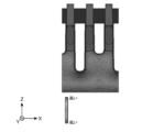
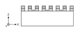
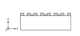
- FIG. 3A and 3B are respectively a plan view and a perspective view of a schematic unit configuration of transistors 10 (or transistors 20) repeatedly formed in the X direction and the Y direction of the semiconductor device 1.
- FIG. 3A and 3B do not show the semiconductor substrate 32, the first source electrode 11 (or the second source electrode 21) for the sake of clarity.
- the Y direction is the direction parallel to the upper surface of the semiconductor layer 40 and in which the first gate trench 17 and the second gate trench 27 extend.
- the X direction is parallel to the upper surface of the semiconductor layer 40 and orthogonal to the Y direction.
- the Z direction is perpendicular to both the X direction and the Y direction and indicates the height direction of the semiconductor device.
- the Y direction may be referred to as the first direction, the X direction as the second direction, and the Z direction as the third direction.
- the transistor 10 includes a first connection portion 18A electrically connecting the first body region 18 and the first source electrode 11.
- the first connection portion 18A is a region of the first body region 18 where the first source region 14 is not formed and contains the same second conductivity type impurity as the first body region 18 .
- the first source regions 14 and the first connecting portions 18A are arranged alternately and periodically in the Y direction. The same is true for the transistor 20 as well.
- a high voltage is applied to the first source electrode 11 and a low voltage is applied to the second source electrode 21, and the second gate electrode 29 (the second gate conductor 25) is applied with the second source electrode 21 as a reference. ), a conduction channel is formed in the vicinity of the second gate insulating film 26 in the second body region 28 when a voltage equal to or higher than the threshold value is applied to the second body region 28 .
- a main current flows through a conduction channel formed in the body region 28 of the second body region 24, the second source region 24, and the second source electrode 21, and the semiconductor device 1 becomes conductive.
- this conduction path there is a PN junction at the contact surface between the second body region 28 and the low-concentration impurity layer 33, which functions as a body diode.
- this main current flows through the metal layer 30 , by increasing the thickness of the metal layer 30 , the cross-sectional area of the main current path can be increased and the on-resistance of the semiconductor device 1 can be reduced.
- a high voltage is applied to the second source electrode 21 and a low voltage is applied to the first source electrode 11, and the first gate electrode 19 (first When a voltage above the threshold is applied to the gate conductor 15), a conducting channel is formed near the first gate insulating film 16 in the first body region 18.
- FIG. 1 second source electrode 21-second connection portion 28A-second body region 28-low concentration impurity layer 33-semiconductor substrate 32-metal layer 30-semiconductor substrate 32-low concentration impurity layer 33-first
- a main current flows through a conduction channel formed in the body region 18 of the semiconductor device--the first source region 14--the first source electrode 11, and the semiconductor device 1 becomes conductive.
- this conduction path there is a PN junction at the contact surface between the first body region 18 and the low-concentration impurity layer 33, which functions as a body diode.
- FIG. 4 shows, of the constituent elements of the semiconductor device 1, a semiconductor layer 40 (low-concentration semiconductor layer 40) including the first body region 18, the second body region 28, the first active region 112, and the second active region 122.
- FIG. 4 is a plan view showing an example of the shape of an impurity layer 33) in a plan view; Although not shown in FIG. 4, both the first gate trench 17 and the second gate trench 27 extend in the Y direction.
- the first active region 112 is the minimum area that includes all the portions in which a conductive channel is formed when a voltage equal to or higher than the threshold is applied to the first gate electrode 19 (first gate conductor 15) of the transistor 10. point to The portion where the conduction channel is formed is the portion where each of the plurality of first gate trenches 17 is adjacent to the first source region 14 .
- the first active region 112 is included in the first body region 18 in plan view of the semiconductor layer 40 .
- the second active region 122 is the minimum area that includes all the portions where a conductive channel is formed when a voltage above the threshold is applied to the second gate electrode 29 (second gate conductor 25) of the transistor 20. Point.
- the portion where the conduction channel is formed is the portion where each of the plurality of second gate trenches 27 is adjacent to the second source region 24 .
- the second active region 122 is included in the second body region 28 in plan view of the semiconductor layer 40 .
- a region of the first region A1 surrounding the first active region 112 is called a first peripheral region, and a region of the second region A2 surrounding the second active region 122 is called a second peripheral region.
- a vertical field effect transistor with a single configuration can be generally recognized as being formed by only one side (transistor 10) of a vertical field effect transistor with a dual configuration.
- a drain electrode pad may be further provided on the surface side of the semiconductor layer 40 having the source electrode pad 116 and the gate electrode pad 119 . In this case, it is necessary to form a drain extraction structure electrically connected to the semiconductor substrate 32 provided on the back side of the semiconductor layer 40 from the front side of the semiconductor layer 40 .
- the potential difference between the first source electrode 11 and the second source electrode 21 is the source-source voltage (VSS [V]).
- VSS [V] the specification maximum voltage between source and source
- the specification maximum voltage between the source and the source may simply be referred to as the breakdown voltage or the drain breakdown voltage.
- a PN junction is provided at the boundary between the first body region 18 and the low-concentration impurity layer 33, and a depletion layer is formed across the PN junction.
- a structure that allows the depletion layer to spread sufficiently when the transistor 10 is off is required, and the carrier concentration (resistivity) and thickness of the low-concentration impurity layer 33 must be appropriately designed. .
- the low-concentration impurity layer 33 In order for the depletion layer to spread sufficiently, the low-concentration impurity layer 33 needs to have a low carrier concentration (high resistivity) and a large thickness. Since the thickness of the low-concentration impurity layer 33 can be made relatively thick when viewed from the tip of the first gate trench 17, the first gate trench 17 is preferably shallow for the purpose of improving the drain breakdown voltage.
- VSS and BVSSS. ] the dual configuration vertical field effect transistor, so it is described as VSS and BVSSS. ]
- VDSS [V] the maximum drain-source voltage specification
- the source-source interval is conveniently called the drain-source interval, and VDS and BVDSS are used for explanation.
- the first gate trench 17 is formed from the upper surface of the semiconductor layer 40 to a depth that contacts the first source region 14 , penetrates the first body region 18 , and reaches a portion of the low-concentration impurity layer 33 . be.
- the current flowing along the tip of the first gate trench 17 flows with relatively reduced conduction resistance even in the low-concentration impurity layer 33. Become. However, after passing the tip of the first gate trench 17 , the current flows with resistance corresponding to the resistivity of the low-concentration impurity layer 33 .
- the first gate trench 17 is relatively shallow, the current flows through the low-concentration impurity layer 33 to the semiconductor substrate 32 over a relatively long distance. Conversely, when the first gate trench 17 is relatively deep, the current flows through the interior of the low-concentration impurity layer 33 to the semiconductor substrate 32 in a relatively short distance. Therefore, for the purpose of reducing the resistance of the current flowing through the low-concentration impurity layer 33, the first gate trench 17 is preferably deep.
- the potential distribution of the low-concentration impurity layer 33 changes. Since the first gate trench 17 is a trench whose tip reaches a portion of the low-concentration impurity layer 33, the potential distribution in the low-concentration impurity layer 33 varies depending on its width, interval, and depth. change the way
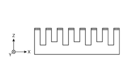
- FIG. 5A is Comparative Example 1 in Embodiment 1, and has a structure in which all the first gate trenches 17 are uniformly formed with a certain depth Da [nm].
- FIG. 6A shows Comparative Example 2 of Embodiment 1, which has a structure in which all first gate trenches 17 are uniformly formed with a certain depth Db [nm] (Da ⁇ Db).
- Comparative Example 1 shows results when the first gate trenches 17 are uniformly and relatively shallow compared to Comparative Example 2 (FIGS. 6A and 6B).
- Comparative Example 2 shows the results when the first gate trenches 17 are uniformly and relatively deep compared to Comparative Example 1 (FIGS. 5A and 5B). is.
- the depth of the first gate trench 17 is 100 nm.
- the low-concentration impurity layer 33 when viewed from the tip of the first gate trench 17, the low-concentration impurity layer 33 is relatively thicker than that in FIG. 6B.
- the interval between the equipotential lines near the tip of the first gate trench 17 is widened. This means that the electric field strength in the low-concentration impurity layer 33 is relatively weak.
- FIGS. 5C and 6C show the results of simulating the electric field intensity [V/cm] distribution when the potential distribution is as shown in FIGS. 5B and 6B, respectively.
- the structurally highest electric field strength is at the central portion of the tip of the first gate trench 17, and the difference in electric field strength at this position is compared with Comparative Example 1 (FIG. 5C).
- Example 2 FIGG. 6C
- it is 0.02 MV/cm.
- the present inventors conducted extensive studies and found that by mixing a plurality of first gate trenches 17 with different depths, all the first gate trenches 17 can be It has been found that the characteristics of the transistor 10 can be improved as compared with the case where the depth of the gate trench 17 is uniform. In the following, the effects of the mixture of first gate trenches 17 having different depths from the upper surface of the semiconductor layer 40 on the characteristics of the transistor 10 will be described.
- the difference in the depth of the first gate trench 17, which is the object of this disclosure, is not a variation that cannot be avoided in manufacturing, but a difference due to design intentionally expressed by setting a target value.
- first gate trenches 17 having a depth of Da [nm] and having a depth of Db [nm], and having two depths (Da ⁇ Db)
- Da ⁇ Db depths
- first gate trench 17 or the second gate trench 27 the one with the depth Da is called the third gate trench 171
- the fourth gate trench 172 the one with the depth Db is called the fourth gate trench 172.
- the third gate trench 171 becomes a relatively shallow gate trench
- the fourth gate trench 172 becomes a relatively deep gate trench.
- a gate conductor and a gate insulating film provided in the third gate trench 171 are referred to as a third gate conductor 151 and a third gate insulating film 161, respectively.
- a gate conductor and a gate insulating film provided in the fourth gate trench 172 are referred to as a fourth gate conductor 152 and a fourth gate insulating film 162, respectively.
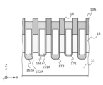
- FIG. 7A is a schematic view of part of the transistor 10 when viewed in cross section in the XZ plane, and includes components above the interlayer insulating layer 34 such as the first source electrode 11 and components below the interlayer insulating layer 34 including the semiconductor substrate 32. FIG. are omitted from the illustration.
- the third gate trenches 171 and the fourth gate trenches 172 have the same width, and the third gate trenches 171 and the fourth gate trenches 172 are alternately arranged at regular intervals. It is
- FIG. 7A the potential [V ] is shown in FIG. 7B, and the simulation result of the electric field intensity [V/cm] at that time is shown in FIG. 7C.
- the potential in the drift layer 33 is generally pushed downward due to the presence of the fourth gate trench 172, and is relatively equal to the equipotential lines near the third gate trench 171.
- the intervals are wider. As a result, the electric field intensity at the center of the tip of the third gate trench 171 is reduced.
- the depth Da of the third gate trenches 171 in FIG. 7A is the same as the depth Da of the first gate trenches 17 in FIG. 5A (comparative example 1), but all the first gate trenches 17 have the same depth. It can be seen that the electric field strength in the central portion of the tip of the third gate trench 171 is reduced compared to FIG. The reason why the electric field strength at the center of the tip of the third gate trench 171 is reduced despite the same depth Da is that the fourth gate trench 172 pushes down the potential toward the low-concentration impurity layer 33. This is because the fourth gate trench 172 deeper than the third gate trench 171 exists in the vicinity of the third gate trench 171 . In other words, this effect cannot be obtained in the conventional structure in which all the first gate trenches 17 have the same depth.
- the electric field intensity at the center of the tip of the fourth gate trench 172 increases.
- the depth of the first gate trenches 17 in FIG. 6A (Comparative Example 2) is the same Db as the depth of the fourth gate trenches 172 in FIG. are unified.
- 6C and 7C the electric field intensity at the tip center of the fourth gate trench 172 in FIG. 7C is higher than the electric field intensity at the tip center of the first gate trench 17 in FIG. 6C. I know it's stronger.
- FIG. 7C which is an embodiment of the present disclosure, the number of fourth gate trenches 172 where the electric field intensity at the center of the tip increases is reduced (approximately halved) compared to FIG. 6C.
- the resistance to deterioration of reliability is improved structurally, and the structure does not immediately affect the deterioration of reliability even when an electric field intensity increased more than conventionally occurs.
- the essence for enjoying the effects of the present disclosure is that, unlike the conventional structure, all the first gate trenches 17 are not made to have the same depth, and the relatively deep fourth gate trenches 172 are relatively deep.
- the third gate trenches 171 should be provided with an appropriate number, distance, and period. With such a structure, while the electric field strength at the center of the tip of the third gate trench 171 is reduced, the upper limit of the electric field strength that leads to the deterioration of reliability can be improved, and the resistance can be improved.
- the fourth gate trenches 172 are preferably arranged on both sides so as to sandwich the third gate trenches 171 in the X direction so as to reduce the electric field strength at the center of the tip of the third gate trenches 171, and most effectively.
- This arrangement is a structure in which one third gate trench 171 and one fourth gate trench 172 are alternately arranged in the X direction.
- the number of third gate trenches 171 sandwiched between the closest paired fourth gate trenches 172 in the X direction may be plural.
- An example is shown in FIG. If the number of the third gate trenches 171 provided in the transistor 10 is n (n is an integer equal to or greater than 1), the number of the fourth gate trenches 172 provided in the transistor 10 is 2 or more (n+1). The following are preferable.
- the one located at both ends in the X direction is designated as the fourth gate trench 172, and the rest is designated as the third gate trench 171. is preferred. With such an arrangement, the electric field intensity at the center of the tip of the third gate trench 171 provided in the first active region 112 can be suppressed.
- first gate trenches 17 provided in the first active region 112 of the transistor 10 are paired most adjacently in the X direction with the fourth gate trenches 172 having one or more third gate trenches therebetween.
- a structure sandwiching a trench 171 is defined as a unit structure, and the unit structures are periodically installed in the X direction. preferably shared with
- the first gate trenches 17 provided in the first active region 112 of the transistor 10 are arranged in the row of the third gate trenches 171 in the X direction periodically at regular intervals in the fourth gate trenches.
- a gate trench 172 is preferably provided.
- the first gate trench 17 consists of n third gate trenches 171 and n+1 fourth gate trenches 172, it is placed in the transistor 10 (first active region 112).
- the first gate trenches 17 one at both ends in the X direction is designated as the fourth gate trench 172, and the third gate trench 171 and the fourth gate trench 172 are alternately arranged one by one. can be installed. At this time, it is possible to suppress the electric field intensity at the tip center of all the third gate trenches 171, which is preferable.
- the interval Laa [ ⁇ m] between the third gate trenches 171 is preferably constant. Further, it is preferable that the interval Lbb [ ⁇ m] between the fourth gate trenches 172 is constant.
- the third gate trenches 171 and the fourth gate trenches 172 can be arranged with the same density as conductive channels, which is effective in reducing the on-resistance.
- the gate trenches (the first gate trench 17 or the second gate trench 27, or the third gate trench 171 or the fourth gate trench 172) targeted in the present disclosure are all It contributes to the formation of a conducting channel and contains the gate conductor (first gate conductor 15 or second gate conductor 25 or third gate conductor 151 or fourth gate conductor 152).
- the third gate conductor 151 and the fourth gate conductor 152 are at the same potential in driving the transistor 10, and the voltage applied to the first gate electrode 19 will cause the third gate conductor 151 and the fourth gate conductor 151 to be at the same potential. It is equally applied to gate conductor 152 .
- the first gate trenches 17 (the third gate trenches 171 and the fourth gate trenches 172) referred to in the present disclosure all have a portion contacting the first source region 14 at the top and the first gate trench 17 at the bottom. It has a portion in contact with the body region 18 .
- the difference ⁇ ( Db ⁇ Da) [nm] between the depth Da of the third gate trench 171 and the depth Db of the fourth gate trench 172, and the drain breakdown voltage VDS of the transistor 10 and on-resistance.
- the withstand voltage shown in Table 1 was calculated under two conditions. Based on condition A, in which the resistivity and thickness of the low-concentration impurity layer 33 are not changed at each level, and the shape of level 2 as a reference, according to an increase in the depth Db of the fourth gate trench 172, The condition B is such that the thickness of the low-concentration impurity layer 33 is also increased. Level 1 corresponds to FIGS. 5A, 5B, and 5C, and Level 2 corresponds to FIGS. 7A, 7B, and 7C. For condition B, simulations are performed only for levels 3-7.
- the difference between the depth of the third gate trench 171 and the depth of the fourth gate trench 172 is preferably 160 nm or more. If ⁇ 160 nm, the breakdown voltage can be improved as shown in Table 1 or FIG. 9 by adjusting the thickness of the low-concentration impurity layer 33 . If there is little need to increase the breakdown voltage margin, the increased breakdown voltage can be used to reduce the on-resistance by adjusting the resistivity and thickness of the low-concentration impurity layer 33 . Even if ⁇ 160 nm, a certain effect can be obtained, but in order to reduce the conduction resistance of the low-concentration impurity layer 33 while ensuring a sufficient breakdown voltage margin, ⁇ 160 nm is adjusted. is desirable.
- a mask layer 36 made of oxide or the like is formed on the upper surface of the semiconductor layer 40 (semiconductor substrate 32 and low-concentration impurity layer 33).
- the resist applied on the mask layer 36 is patterned to form openings at regular intervals in the X direction.
- the width of the opening of the resist in the X direction finally becomes the internal width of the fourth gate trench 172 .
- the transistor 10 is formed so that the internal width and spacing of the third gate trench 171 and the fourth gate trench 172 are equal, the width of the non-opening portion in the X direction covered with the resist in FIG. 12B is , patterning is performed so as to be approximately three times the width of the opening in the X direction from which the resist is removed.
- the resist opening is etched to remove the mask layer 36 .
- the mask layer 36 may not be completely removed and remain on the semiconductor layer 40 with a constant thickness, it is desirable that the mask layer 36 be completely removed as shown in FIG. 12C.
- the remaining resist is patterned again to periodically provide portions where the mask layer 36 is newly exposed in the X direction.
- the width of the opening newly provided in the resist in the X direction finally becomes the internal width of the third gate trench 171 .
- the portions of the mask layer 36 newly exposed in the process of FIG. 12D are etched to remove the mask layer 36 leaving a certain thickness on the semiconductor layer 40 .
- the partially remaining mask layer 36 is used as a mask to etch the mask layer 36 and the semiconductor layer 40 .
- the mask layer 36 is selectively thinly applied only at the locations that will later become the third gate trenches 171 .
- etching of the semiconductor layer 40 progresses from the beginning in the portions where the mask layer 36 was originally removed.
- the mask layer 36 is first completely removed, and then the semiconductor layer 40 directly under it starts to be etched. Since the semiconductor layer 40 is being etched in , trenches having different depths are alternately formed in the semiconductor layer 40 .
- the third gate trench 171 and the fourth gate trench 172 are formed by manipulating the thickness of the mask layer 36, the etching conditions, the remaining thickness of the mask layer 36 left on the upper surface of the semiconductor layer 40 in the step shown in FIG. 12E, and the like. depth difference can be controlled.
- the inner width of the third gate trench 171 and the inner width of the fourth gate trench 172, or the distance between the third gate trenches 171, the distance between the fourth gate trenches 172, the distance between the third gate trench 171 and the fourth gate trench 172, 4 and the gate trench 172 can be freely designed by controlling the dimension for patterning the resist.
- the first gate trench 17 is composed of the third gate trench 171 and the fourth gate trench 172, and the third gate conductor 151 provided in the third gate trench 171 and the third gate insulating film. 161 , and the fourth gate conductor 152 provided in the fourth gate trench 172 and the fourth gate insulating film 162 .
- the first gate trench 17 is composed of the third gate trench 171 and the fourth gate trench 172 in the transistor 10A according to the second embodiment.
- a configuration having a third gate conductor 151A and a third gate insulating film 161A provided in the gate trench 171, and a fourth gate conductor 152A and a fourth gate insulating film 162A provided in the fourth gate trench 172 is an example of
- the same reference numerals are given to the same constituent elements as those of the transistor 10, and the detailed explanation thereof will be omitted. explain.
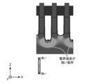
- FIG. 13 shows a schematic diagram of the shape of the transistor 10A in the second embodiment.
- FIG. 13 is a schematic view of a part of the transistor 10A when viewed in cross section in the XZ plane, and includes components above the interlayer insulating layer 34 such as the first source electrode 11 and components below the interlayer insulating layer 34 including the semiconductor substrate 32. are omitted from the illustration.
- Embodiment 2 The difference between Embodiment 2 and Embodiment 1 is that the shapes of the third gate insulating film 161A and the fourth gate insulating film 162A are different.
- the fourth gate insulating film 162A is thicker on the bottom side of the fourth gate trench 172 than on the upper side of the fourth gate trench 172 .
- the fourth gate trench 172 is a relatively deep trench, so the electric field intensity at the center of the tip increases. If the fourth gate insulating film 162A were extremely thin, the structure would not be able to withstand the increased electric field intensity, and there would be a possibility that a current would leak between the drain and the gate. For this reason, if the fourth gate insulating film 162A is formed thick only on the bottom side of the fourth gate trench 172 so as to widely cover the tip of the fourth gate trench 172 where the electric field strength is particularly increased, preferable.
- FIG. 13 exemplifies a configuration in which the fourth gate insulating film 162A is uniformly thick on the bottom side of the fourth gate trench 172, but the effect of the second embodiment is obtained only with the shape of FIG. is not limited to
- the fourth gate insulating film 162A may be provided along the shape of the fourth gate trench 172 so as to be thick only on the side and bottom sides of a part, and the thickened part is an insulating material made of a different material. It may have a multilayer structure of films.
- the thickness of the third gate insulating film 161A may be the same regardless of whether it is the sidewall or the bottom of the third gate trench 171, like the third gate insulating film 161 in the first embodiment. This is because the electric field strength generated at the tip of the third gate trench 171 does not excessively increase, so that it is not necessary to thicken the third gate insulating film 161A. Therefore, it is desirable that the fourth gate insulating film 162A, which needs to be more resistant to relatively increasing electric field intensity, have a thicker portion than the third gate insulating film 161A. In particular, it is desirable that the fourth gate insulating film 162A is thickly installed on the bottom side of the fourth gate trench.
- the electric field strength at the tip of the third gate trench 171 may increase to some extent. be.
- the bottom side of the third gate insulating film 161A may be thickened.
- the third gate insulating film 161A and the fourth gate insulating film 162A may have the same thickness, or the fourth gate insulating film 162A may be relatively thicker. may have been
- the transistor 10 is an example in which the low-concentration impurity layer 33 is composed of one layer.
- the transistor 10B according to the third embodiment is an example of a structure having a two-layer low-concentration impurity layer 33B in the transistor 10B according to the third embodiment.
- the same reference numerals are given to the same constituent elements as those of the transistor 10, and the detailed explanation thereof will be omitted. explain.
- FIG. 14 shows a schematic diagram of the shape of the transistor 10B in the third embodiment.
- FIG. 14 is a schematic view of a part of the transistor 10B when viewed in cross section in the XZ plane, and shows components above the interlayer insulating layer 34 such as the first source electrode 11 and components below the interlayer insulating layer 34 including the semiconductor substrate 32. are omitted from the illustration.
- the low-concentration impurity layer 33B of the transistor 10B has a two-layer structure.
- the low-concentration impurity layer 33B is formed by stacking a second low-concentration impurity layer 332 on a semiconductor substrate 32 (not shown) and then stacking a first low-concentration impurity layer 331 thereon.
- the first low-concentration impurity layer 331 is a layer exhibiting a lower resistivity than the second low-concentration impurity layer 332 , and the second low-concentration impurity layer 332 has a lower resistivity than the first low-concentration impurity layer 331 . It is a layer that exhibits high resistivity. For example, when the impurity concentration inside the low-concentration impurity layer 33B is compared, the concentration of the first-conductivity-type impurity in the first low-concentration impurity layer 331 is higher than that of the first-conductivity-type impurity in the second low-concentration impurity layer 332. higher than the concentration of impurities.
- the tip of the third gate trench 171 is formed to reach the inside of the first low-concentration impurity layer 331 . Furthermore, the tip of the third gate trench 171 is not formed to reach the second low-concentration impurity layer 332 through the first low-concentration impurity layer 331 . Also, the tip of the fourth gate trench 172 is formed to reach the inside of the second low-concentration impurity layer 332 . Furthermore, the tip of the fourth gate trench 172 is not formed to reach the semiconductor substrate 32 through the second low-concentration impurity layer 332 .
- the tip of the third gate trench 171 When the tip of the third gate trench 171 is placed inside the first low-concentration impurity layer 331 as described above, the main current passing through the conduction channel formed by the third gate trench 171 is The substrate 32 is reached via the first low-concentration impurity layer 331 and the second low-concentration impurity layer 332 directly below the third gate trench 171 . Since the first low-concentration impurity layer 331 has relatively low resistivity, the resistance of the main current flowing through the low-concentration impurity layer 33 can be reduced.
- the electric field intensity generated near the tip of the third gate trench 171 will increase.
- provision of the fourth gate trench 172 inherently reduces the electric field strength near the tip of the third gate trench 171 . Therefore, the increase in electric field strength can be offset to some extent.
- the first low-concentration impurity layer 331 Resistivity or thickness can be selected appropriately.
- the second low-concentration impurity layer 332 has a relatively high resistivity.
- the electric field intensity generated near the tip of 172 can be reduced.
- the effect is that the structure of the present disclosure reduces the electric field strength near the tip of the third gate trench 171, while reducing the side effect of originally increasing the electric field strength near the tip of the fourth gate trench 172. convenient for
- the main current passing through the conduction channel formed by the fourth gate trench 172 passes through the second low-concentration impurity layer 332 immediately below the fourth gate trench 172 to reach the semiconductor substrate 32 .
- the second low-concentration impurity layer 332 has a relatively high resistivity, although the resistance of the main current flowing through the low-concentration impurity layer 33 is increased, the fourth gate trench 172 is relatively Since it is formed deep, the distance over which the main current flows through the second low-concentration impurity layer 332 does not have to be excessively large.
- the low-concentration impurity layer 33B is appropriately configured in two stages, thereby reducing side effects related to the third gate trench 171 and the fourth gate trench 172 that occur in the present disclosure. can do.
- the structure of the vertical field effect transistor is first described by taking a dual configuration as an example, the gate trench of the first transistor is the first gate trench, and the gate trench of the second transistor is the second gate trench. and To avoid confusion, the relatively shallow gate trench has been referred to as the third gate trench and the relatively deep gate trench has been referred to as the fourth gate trench throughout this disclosure.
- the structure of the vertical field effect transistor that can obtain the effect is not limited to the dual structure. Therefore, it is not necessary to distinguish between the first transistor and the second transistor, and the third gate trench can be called the first gate trench, and the fourth gate trench can be called the second gate trench.
- a semiconductor device comprising a vertical field effect transistor according to the present invention can be widely used as a device for controlling the conduction state of a current path.
Landscapes
- Engineering & Computer Science (AREA)
- Microelectronics & Electronic Packaging (AREA)
- Power Engineering (AREA)
- Physics & Mathematics (AREA)
- Ceramic Engineering (AREA)
- Condensed Matter Physics & Semiconductors (AREA)
- General Physics & Mathematics (AREA)
- Computer Hardware Design (AREA)
- Manufacturing & Machinery (AREA)
- Electrodes Of Semiconductors (AREA)
- Insulated Gate Type Field-Effect Transistor (AREA)
Abstract
半導体装置(1)は、第1の方向に延在する第1のゲートトレンチ(17)および第1のゲートトレンチ(17)よりも深く形成された第2のゲートトレンチ(27)と、第1のゲートトレンチ(17)の内部に形成された第1のゲート絶縁膜(16)および第1のゲート導体(15)と、第2のゲートトレンチ(27)の内部に形成された第2のゲート絶縁膜(26)および第2のゲート導体(25)と、を有する縦型電界効果トランジスタ(10)であって、第1のゲート導体(15)と第2のゲート導体(25)とは同電位であって、第1のゲートトレンチ(17)の本数をnとすると、第2のゲートトレンチ(27)の本数は2以上n+1以下であり、低濃度不純物層(33)の上面と平行で第1の方向に直交する第2の方向において、第1のゲートトレンチ(17)と第2のゲートトレンチ(27)とが設置される領域の最端は前記第2のゲートトレンチ(27)が設置される。
Description
本開示は、半導体装置に関し、特には、チップサイズパッケージ型の半導体装置に関する。
ゲートトレンチを備える縦型電界効果トランジスタでは、耐圧とオン抵抗にトレードオフの関係があることが知られている。
ゲートトレンチを備える縦型電界効果トランジスタにおいて、耐圧を維持しながらオン抵抗を低減すると共に、ドレイン-ソース間に電圧を印加する際にゲートトレンチの先端付近に生じる電界強度を低減して、信頼性の低下に対する耐性を高めることが求められている。
特許文献1および特許文献2には、縦型電界効果トランジスタの構造が開示されており、トレードオフの関係にある特性を良化する構造が示されている。
上記の課題を解決するために、本開示に係る半導体装置は、フェイスダウン実装が可能なチップサイズパッケージ型の半導体装置であって、第1導電型の不純物を含む前記第1導電型の半導体基板と、前記半導体基板上に接して形成され、前記半導体基板の前記第1導電型の不純物の濃度より低い濃度の前記第1導電型の不純物を含む前記第1導電型の低濃度不純物層と、前記低濃度不純物層に形成された前記第1導電型と異なる第2導電型のボディ領域と、前記ボディ領域に形成された前記第1導電型のソース領域と、前記ボディ領域および前記ソース領域と電気的に接続されたソース電極と、前記低濃度不純物層上面から、前記ボディ領域を貫通して前記低濃度不純物層の一部までの深さに形成され、前記ソース領域と接触する部分を有し、前記低濃度不純物層の上面と平行な第1の方向に延在する第1のゲートトレンチと、前記低濃度不純物層上面から、前記ボディ領域を貫通して前記第1のゲートトレンチよりも深く形成され、前記ソース領域と接触する部分を有し、前記第1の方向に延在する第2のゲートトレンチと、前記第1のゲートトレンチの内部に形成された第1のゲート絶縁膜と、前記第1のゲート絶縁膜上に形成された第1のゲート導体と、前記第2のゲートトレンチの内部に形成された第2のゲート絶縁膜と、前記第2のゲート絶縁膜上に形成された第2のゲート導体と、を有する縦型電界効果トランジスタであり、前記第1のゲート導体と前記第2のゲート導体とは同電位であって、前記第1のゲートトレンチの本数をn(nは1以上の整数)とすると、前記第2のゲートトレンチの本数は2以上n+1以下であり、前記低濃度不純物層の上面と平行で前記第1の方向に直交する第2の方向において、前記第1のゲートトレンチと前記第2のゲートトレンチとが設置される領域の最端は前記第2のゲートトレンチが設置される半導体装置であることを特徴とする。
この構成によれば、オン抵抗を低減すると共に、ドレイン-ソース間に電圧を印加する際に、信頼性低下の要因となる電界強度に対しての耐性を高めることができる。
本開示は、耐圧を維持しながらオン抵抗を低減すると共に、信頼性向上を実現できる半導体装置を提供することを目的とする。
以下、本開示の一態様に係る半導体装置の具体例について、図面を参照しながら説明する。ここで示す実施形態は、いずれも本開示の一具体例を示すものである。従って、以下の実施形態で示される数値、形状、構成要素、構成要素の配置および接続形態、ならびに、ステップ(工程)およびステップの順序等は、一例であって本開示を限定する趣旨ではない。また、各図は、模式図であり、必ずしも厳密に図示されたものではない。各図において、実質的に同一の構成に対しては同一の符号を付しており、重複する説明は省略または簡略化する。
(実施形態1)
[1.半導体装置の構造]
以下では、本開示における縦型電界効果トランジスタの構造についてデュアル構成を例にとって説明する。デュアル構成であることは必須ではなく、シングル構成の縦型電界効果トランジスタであってもよく、トリプル以上の構成の縦型電界効果トランジスタであってもよい。
[1.半導体装置の構造]
以下では、本開示における縦型電界効果トランジスタの構造についてデュアル構成を例にとって説明する。デュアル構成であることは必須ではなく、シングル構成の縦型電界効果トランジスタであってもよく、トリプル以上の構成の縦型電界効果トランジスタであってもよい。
図1は半導体装置の構造の一例を示す断面図である。図2Aはその平面図であり、半導体装置の大きさや形状、電極パッドの配置は一例である。図2Bは、半導体装置に流れる主電流を模式的に示す断面図である。図1および図2Bは、図2AのI-Iにおける切断面である。
図1および図2Aに示すように、半導体装置1は、半導体層40と、金属層30と、半導体層40内の第1の領域A1に形成された第1の縦型電界効果トランジスタ10(以下、「トランジスタ10」とも称する。)と、半導体層40内の第2の領域A2に形成された第2の縦型電界効果トランジスタ20(以下、「トランジスタ20」とも称する。)と、を有する。ここで、図2Aに示すように、第1の領域A1と第2の領域A2とは、半導体層40の平面視において互いに隣接する。図2Aでは第1の領域A1と第2の領域A2の仮想的な境界線90を破線で示している。
半導体層40は、半導体基板32と低濃度不純物層33とが積層されて構成される。半導体基板32は、半導体層40の裏面側に配置され、第1導電型の不純物を含む第1導電型のシリコンからなる。低濃度不純物層33は、半導体層40の表面側に配置され、半導体基板32に接触して形成され、半導体基板32の第1導電型の不純物の濃度より低い濃度の第1導電型の不純物を含んで、第1導電型である。
低濃度不純物層33は、例えば、エピタキシャル成長により半導体基板32上に形成されてもよい。なお、低濃度不純物層33はトランジスタ10およびトランジスタ20に共通するドリフト層でもあり、本明細書中ではドリフト層とよぶこともある。
金属層30は、半導体層40の裏面側に接触して形成され、銀(Ag)もしくは銅(Cu)からなる。なお、金属層30には、金属材料の製造工程において不純物として混入する金属以外の元素が微量に含まれていてもよい。また、金属層30は半導体層40の裏面側の全面に形成されていてもいなくてもどちらでもよい。
図1および図2Aに示すように、低濃度不純物層33の第1の領域A1には、第1導電型と異なる第2導電型の不純物を含む第2導電型の第1のボディ領域18が形成されている。第1のボディ領域18には、第1導電型の不純物を含む第1導電型の第1のソース領域14、第1のゲート導体15、および第1のゲート絶縁膜16が形成されている。第1のゲート絶縁膜16は、半導体層40の上面から第1のソース領域14および第1のボディ領域18を貫通して低濃度不純物層33の一部までの深さに形成された複数の第1のゲートトレンチ17の内部に形成され、第1のゲート導体15は第1のゲートトレンチ17の内部で、第1のゲート絶縁膜16上に形成されている。
第1のソース電極11は部分12と部分13とからなり、部分12は、部分13を介して第1のソース領域14および第1のボディ領域18に接続されている。第1のゲート導体15は半導体層40の内部に埋め込まれた、埋め込みゲート電極であり、第1のゲート電極パッド119に電気的に接続される。
第1のソース電極11の部分12は、フェイスダウン実装におけるリフロー時にはんだと接合される層であり、限定されない一例として、ニッケル、チタン、タングステン、パラジウムのうちのいずれか1つ以上を含む金属材料で構成されてもよい。部分12の表面には、金などのめっきが施されてもよい。
第1のソース電極11の部分13は、部分12と半導体層40とを接続する層であり、限定されない一例として、アルミニウム、銅、金、銀のうちのいずれか1つ以上を含む金属材料で構成されてもよい。
低濃度不純物層33の第2の領域A2には、第2導電型の不純物を含む第2導電型の第2のボディ領域28が形成されている。第2のボディ領域28には、第1導電型の不純物を含む第1導電型の第2のソース領域24、第2のゲート導体25、および第2のゲート絶縁膜26が形成されている。第2のゲート絶縁膜26は、半導体層40の上面から第2のソース領域24および第2のボディ領域28を貫通して低濃度不純物層33の一部までの深さに形成された複数の第2のゲートトレンチ27の内部に形成され、第2のゲート導体25は第2のゲートトレンチ27の内部で、第2のゲート絶縁膜26上に形成されている。
第2のソース電極21は部分22と部分23とからなり、部分22は、部分23を介して第2のソース領域24および第2のボディ領域28に接続されている。第2のゲート導体25は半導体層40の内部に埋め込まれた、埋め込みゲート電極であり、第2のゲート電極パッド129に電気的に接続される。
第2のソース電極21の部分22は、フェイスダウン実装におけるリフロー時にはんだと接合される層であり、限定されない一例として、ニッケル、チタン、タングステン、パラジウムのうちのいずれか1つ以上を含む金属材料で構成されてもよい。部分22の表面には、金などのめっきが施されてもよい。
第2のソース電極21の部分23は、部分22と半導体層40とを接続する層であり、限定されない一例として、アルミニウム、銅、金、銀のうちのいずれか1つ以上を含む金属材料で構成されてもよい。
トランジスタ10およびトランジスタ20の上記構成により、半導体基板32は、トランジスタ10の第1のドレイン領域およびトランジスタ20の第2のドレイン領域が共通化された、共通ドレイン領域として機能する。低濃度不純物層33の、半導体基板32に接する側の一部も、共通ドレイン領域として機能する場合がある。また金属層30はトランジスタ10のドレイン電極およびトランジスタ20のドレイン電極が共通化された、共通ドレイン電極として機能する。
図1に示すように、第1のボディ領域18は、開口を有する層間絶縁層34で覆われ、層間絶縁層34の開口を通して、第1のソース領域14に接続される第1のソース電極11の部分13が設けられている。層間絶縁層34および第1のソース電極の部分13は、開口を有するパッシベーション層35で覆われ、パッシベーション層35の開口を通して第1のソース電極の部分13に接続される部分12が設けられている。
第2のボディ領域28は、開口を有する層間絶縁層34で覆われ、層間絶縁層34の開口を通して、第2のソース領域24に接続される第2のソース電極21の部分23が設けられている。層間絶縁層34および第2のソース電極の部分23は、開口を有するパッシベーション層35で覆われ、パッシベーション層35の開口を通して第2のソース電極の部分23に接続される部分22が設けられている。
したがって複数の第1のソース電極パッド116および複数の第2のソース電極パッド126は、それぞれ第1のソース電極11および第2のソース電極21が半導体装置1の表面に部分的に露出した領域、いわゆる端子の部分を指す。同様に、1以上の第1のゲート電極パッド119および1以上の第2のゲート電極パッド129は、それぞれ第1のゲート電極19(図1、図2A、図2Bには図示せず。)および第2のゲート電極29(図1、図2A、図2Bには図示せず。)が半導体装置1の表面に部分的に露出した領域、いわゆる端子の部分を指す。
半導体装置1において、例えば、第1導電型をN型、第2導電型をP型として、第1のソース領域14、第2のソース領域24、半導体基板32、および、低濃度不純物層33はN型半導体であり、かつ、第1のボディ領域18および第2のボディ領域28はP型半導体であってもよい。
また、半導体装置1において、例えば、第1導電型をP型、第2導電型をN型として、第1のソース領域14、第2のソース領域24、半導体基板32、および、低濃度不純物層33はP型半導体であり、かつ、第1のボディ領域18および第2のボディ領域28はN型半導体であってもよい。
以下の説明では、トランジスタ10とトランジスタ20とが、第1導電型をN型、第2導電型をP型とした、いわゆるNチャネル型トランジスタの場合として、半導体装置1の導通動作について説明する。
なお、ここではトランジスタ10とトランジスタ20については、機能、特性、構造等に何ら差異のない、対称性が備わることを前提に説明した。図1、図2A、図2Bも対称性を前提に描画しているが、本開示におけるチップサイズパッケージ型の、デュアル構成の縦型電界効果トランジスタにおいては、対称性は必ずしも必要な条件ではない。
[2.縦型電界効果トランジスタの動作]
図3Aおよび図3Bは、それぞれ、半導体装置1のX方向およびY方向に繰り返し形成される、トランジスタ10(またはトランジスタ20)の略単位構成の、平面図および斜視図である。図3Aおよび図3Bでは、分かりやすくするために半導体基板32、第1のソース電極11(または第2のソース電極21)は図示していない。
図3Aおよび図3Bは、それぞれ、半導体装置1のX方向およびY方向に繰り返し形成される、トランジスタ10(またはトランジスタ20)の略単位構成の、平面図および斜視図である。図3Aおよび図3Bでは、分かりやすくするために半導体基板32、第1のソース電極11(または第2のソース電極21)は図示していない。
なおY方向とは、半導体層40の上面と平行し、第1のゲートトレンチ17および第2のゲートトレンチ27が延在する方向である。またX方向とは、半導体層40の上面と平行し、Y方向に直交する方向のことをいう。Z方向とはX方向にもY方向にも直交し、半導体装置の高さ方向を示す方向のことをいう。本開示ではY方向のことを第1の方向、X方向のことを第2の方向、Z方向のことを第3の方向と表すこともある。
図3Aおよび図3Bに示すように、トランジスタ10には、第1のボディ領域18と第1のソース電極11とを電気的に接続する第1の接続部18Aが備わる。第1の接続部18Aは、第1のボディ領域18のうち、第1のソース領域14が形成されていない領域であり、第1のボディ領域18と同じ第2導電型の不純物を含む。第1のソース領域14と第1の接続部18Aとは、Y方向に沿って交互に、かつ周期的に繰り返し配置される。トランジスタ20についても同様である。
半導体装置1において、第1のソース電極11に高電圧および第2のソース電極21に低電圧を印加し、第2のソース電極21を基準として第2のゲート電極29(第2のゲート導体25)にしきい値以上の電圧を印加すると、第2のボディ領域28中の第2のゲート絶縁膜26の近傍に導通チャネルが形成される。その結果、第1のソース電極11-第1の接続部18A-第1のボディ領域18-低濃度不純物層33-半導体基板32-金属層30-半導体基板32-低濃度不純物層33-第2のボディ領域28に形成された導通チャネル-第2のソース領域24-第2のソース電極21という経路で主電流が流れて半導体装置1が導通状態となる。なお、この導通経路における、第2のボディ領域28と低濃度不純物層33との接触面にはPNジャンクションがあり、ボディダイオードとして機能している。また、この主電流は金属層30を流れるため、金属層30を厚くすることで、主電流経路の断面積が拡大し、半導体装置1のオン抵抗は低減できる。
同様に、半導体装置1において、第2のソース電極21に高電圧および第1のソース電極11に低電圧を印加し、第1のソース電極11を基準として第1のゲート電極19(第1のゲート導体15)にしきい値以上の電圧を印加すると、第1のボディ領域18中の第1のゲート絶縁膜16の近傍に導通チャネルが形成される。その結果、第2のソース電極21-第2の接続部28A-第2のボディ領域28-低濃度不純物層33-半導体基板32-金属層30-半導体基板32-低濃度不純物層33-第1のボディ領域18に形成された導通チャネル-第1のソース領域14-第1のソース電極11という経路で主電流が流れて半導体装置1が導通状態となる。なお、この導通経路における、第1のボディ領域18と低濃度不純物層33との接触面にはPNジャンクションがあり、ボディダイオードとして機能している。
図4は、半導体装置1の構成要素のうち、第1のボディ領域18と第2のボディ領域28と、第1の活性領域112と第2の活性領域122との、半導体層40(低濃度不純物層33)の平面視における形状の一例を示す平面図である。図4では図示していないが、第1のゲートトレンチ17も第2のゲートトレンチ27も、Y方向に延在している。
第1の活性領域112とは、トランジスタ10の第1のゲート電極19(第1のゲート導体15)にしきい値以上の電圧を印加したときに導通チャネルが形成される部分すべてを内包する最小範囲を指す。導通チャネルが形成される部分とは、複数の第1のゲートトレンチ17の各々が、第1のソース領域14と隣接する部分である。半導体層40の平面視で、第1の活性領域112は第1のボディ領域18に内包される。
第2の活性領域122とはトランジスタ20の第2のゲート電極29(第2のゲート導体25)にしきい値以上の電圧を印加したときに導通チャネルが形成される部分すべてを内包する最小範囲を指す。導通チャネルが形成される部分とは、複数の第2のゲートトレンチ27の各々が、第2のソース領域24と隣接する部分である。半導体層40の平面視で、第2の活性領域122は第2のボディ領域28に内包される。
第1の領域A1のうち第1の活性領域112を取り囲む領域を第1の外周領域とよび、第2の領域A2のうち第2の活性領域122を取り囲む領域を第2の外周領域とよぶ。
シングル構成の縦型電界効果トランジスタについては、概ねデュアル構成の縦型電界効果トランジスタの片側(トランジスタ10)のみで形成されるものと認識してよい。ただしチップサイズパッケージ型では、ソース電極パッド116、ゲート電極パッド119を備える半導体層40の表面側に、さらにドレイン電極パッドを設けることがある。この場合、半導体層40の裏面側に備わる半導体基板32と電気的に接続するドレイン引き出し構造を、半導体層40の表面側から形成しておく必要がある。
[3.ゲートトレンチの深さとトランジスタの特性]
(3-1.ドレイン耐圧)
以降の説明では、半導体装置1について、特に断らない限りトランジスタ10についての構成要素のみを記載することとする。符号も、必要がない限り、トランジスタ10の構成要素に付与されたものを代表して使用する。
(3-1.ドレイン耐圧)
以降の説明では、半導体装置1について、特に断らない限りトランジスタ10についての構成要素のみを記載することとする。符号も、必要がない限り、トランジスタ10の構成要素に付与されたものを代表して使用する。
半導体装置1において、第1のソース電極11と第2のソース電極21との電位差を、ソース-ソース間電圧(VSS[V])とする。半導体装置1の製品仕様書では、用途に応じて、ソース-ソース間仕様最大電圧(BVSSS[V])が設定される。ソース-ソース間仕様最大電圧(BVSSS[V])のことを本開示では単に耐圧、またはドレイン耐圧ということがある。
第1のボディ領域18と低濃度不純物層33の境界にはPNジャンクションが備わっており、PNジャンクションを挟んで空乏層が形成される。ドレイン耐圧を高めるには、トランジスタ10のオフ時における空乏層が十分に拡がることのできる構造が必要であり、低濃度不純物層33のキャリア濃度(抵抗率)や厚さを適切に設計されねばならない。
空乏層が十分に拡がるためには、低濃度不純物層33はキャリア濃度を低く(抵抗率を高く)、厚さを厚くする必要がある。第1のゲートトレンチ17の先端から見て低濃度不純物層33の厚さを相対的に厚くすることができるので、ドレイン耐圧を向上する目的においては第1のゲートトレンチ17は浅い方が好ましい。
ところで本実施形態における説明は、デュアル構成の縦型電界効果トランジスタに基づいたためVSS、BVSSSとして述べたが、シングル構成の縦型電界効果トランジスタである場合はそれぞれ、ドレイン-ソース間電圧(VDS[V])、ドレイン-ソース間仕様最大電圧(BVDSS[V])を用いればよい。
以降はデュアル構成の縦型電界効果トランジスタであっても、ソース-ソース間のことを便宜的にドレイン-ソース間とよび、VDS、BVDSSを用いて説明する。
(3-2.オン抵抗)
第1のゲートトレンチ17は、半導体層40の上面から、第1のソース領域14に接触し、第1のボディ領域18を貫通して低濃度不純物層33の一部までの深さに形成される。第1のソース電極11から共通ドレインである半導体基板32へ向かって流れる電流は、第1のボディ領域18を通過した後、第1のゲートトレンチ17の先端までは第1のゲートトレンチ17に沿って、低濃度不純物層33を流れることになる。
第1のゲートトレンチ17は、半導体層40の上面から、第1のソース領域14に接触し、第1のボディ領域18を貫通して低濃度不純物層33の一部までの深さに形成される。第1のソース電極11から共通ドレインである半導体基板32へ向かって流れる電流は、第1のボディ領域18を通過した後、第1のゲートトレンチ17の先端までは第1のゲートトレンチ17に沿って、低濃度不純物層33を流れることになる。
第1のゲートトレンチ17の先端に沿って流れる電流は、第1のゲート導体15に印加される電圧の影響で、低濃度不純物層33であっても導通抵抗が比較的軽減されて流れることになる。しかし第1のゲートトレンチ17の先端を過ぎると、電流は低濃度不純物層33における抵抗率に応じた抵抗を受けて流れることになる。
このため第1のゲートトレンチ17が相対的に浅い場合は、電流は、半導体基板32まで低濃度不純物層33の内部を相対的に長い距離で流れることになる。逆に第1のゲートトレンチ17が相対的に深い場合は、電流は、半導体基板32まで低濃度不純物層33の内部を相対的に短い距離で流れることになる。したがって低濃度不純物層33を流れる電流の抵抗を低減する目的では、第1のゲートトレンチ17は深い方が好ましい。
(3-3.電界強度と信頼性)
半導体装置1でVDSを大きくしていくと低濃度不純物層33には電位の分布に変化が生じる。第1のゲートトレンチ17は先端が低濃度不純物層33の一部までの深さに形成された溝であるため、その幅や間隔、深さに応じて、低濃度不純物層33における電位の分布の仕方が変わる。
半導体装置1でVDSを大きくしていくと低濃度不純物層33には電位の分布に変化が生じる。第1のゲートトレンチ17は先端が低濃度不純物層33の一部までの深さに形成された溝であるため、その幅や間隔、深さに応じて、低濃度不純物層33における電位の分布の仕方が変わる。
図5Aは本実施形態1における比較例1であり、ある深さDa[nm]で全ての第1のゲートトレンチ17が一様に形成された構造である。図5Aにおいて、第1のゲート導体15への印加電圧がゼロの状態のまま、VDS=BVDSS(ここでは22V)となるまで電圧を印加したときの電位[V]の分布をシミュレーションした結果を図5Bに示す。
また図6Aは本実施形態1における比較例2であり、ある深さDb[nm](Da<Db)で全ての第1のゲートトレンチ17が一様に形成された構造である。図6Aにおいて、第1のゲート導体15への印加電圧がゼロの状態のまま、VDS=BVDSS(ここでは22V)となるまで電圧を印加したときの電位[V]の分布をシミュレーションした結果を図6Bに示す。
比較例1(図5A、図5B)と、比較例2(図6A、図6B)とでは第1のゲートトレンチ17の深さだけを変化させ、PNジャンクションの位置は変わらないものとしている。
比較例1(図5A、図5B)で示すのは比較例2(図6A、図6B)と比べると、第1のゲートトレンチ17が一様に、相対的に浅い場合の結果である。その逆に、比較例2(図6A、図6B)で示すのは比較例1(図5A、図5B)と比べると、第1のゲートトレンチ17が一様に、相対的に深い場合の結果である。比較例1(図5A、図5B)に示す第1のゲートトレンチ17と、比較例2(図6A、図6B)に示す第1のゲートトレンチ17とでは、第1のゲートトレンチ17の深さの差異は100nmである。
図5Bでは、第1のゲートトレンチ17の先端からみると、図6Bと比べて低濃度不純物層33は相対的に厚いため、厚い幅の中にVDS=BVDSSの電位が分布することになり、第1のゲートトレンチ17の先端付近の等電位線の間隔は広くなる。これは低濃度不純物層33内における電界強度が相対的には弱いことを意味している。
これに対して図6Bでは、第1のゲートトレンチ17の先端からみると、図5Bと比べて低濃度不純物層33は相対的に薄いため、薄い幅の中にVDS=BVDSSの電位が分布することになり、第1のゲートトレンチ17の先端付近の等電位線の間隔は狭くなる。これは低濃度不純物層33内における電界強度が相対的には強いことを意味している。
図5C、図6Cはそれぞれ、電位の分布が図5B、図6Bとなるときの電界強度[V/cm]の分布をシミュレーションした結果を濃淡で表したものである。図5C、図6Cによれば構造的に最も電界強度が大きくなるのは第1のゲートトレンチ17の先端の中央部分になり、この位置における電界強度の差を比較例1(図5C)と比較例2(図6C)で比べると0.02MV/cmである。
第1のゲートトレンチ17の近傍における電界強度が一定以上になると、第1のゲート絶縁膜16の付近にキャリアが蓄積され、いわゆるホットエレクトロンとなる。ホットエレクトロンが生じると、第1のゲート導体15へゲート電圧を印加しなくても反転層ができて導通チャネルが形成されるため、トランジスタ10の信頼性が低下する要因となる。
図5C、図6Cによれば電界強度は第1のゲートトレンチ17が深いほど大きくなるため、信頼性低下を防止する観点では第1のゲートトレンチ17は浅い方が好ましい。
[4.浅いゲートトレンチと深いゲートトレンチの混在]
トランジスタ10の特性と第1のゲートトレンチ17の深さは、上記のように密接に関係している。特性によってはトレードオフの関係にあり、すべての特性を良化することは難しく、重視する用途に応じて適切に第1のゲートトレンチ17の深さを設計する必要があった。
トランジスタ10の特性と第1のゲートトレンチ17の深さは、上記のように密接に関係している。特性によってはトレードオフの関係にあり、すべての特性を良化することは難しく、重視する用途に応じて適切に第1のゲートトレンチ17の深さを設計する必要があった。
そこで本発明者らは鋭意検討を重ねた結果、複数の第1のゲートトレンチ17に深さを変えたものを混在させることで、比較例1および比較例2のように、すべての第1のゲートトレンチ17の深さが統一されている場合に比べて、トランジスタ10の特性を向上できることを見出した。以下では第1のゲートトレンチ17において、半導体層40の上面からの深さが異なるものが混在することが、トランジスタ10の特性に及ぼす影響について説明する。
本開示で対象とする、第1のゲートトレンチ17の深さが異なるというのは、製造上どうしても回避できないばらつきではなく、ねらい値を設けて意図的に現わした設計による差異のことである。
まず一例として、図7Aを用いて、複数の第1のゲートトレンチ17で、深さDa[nm]のものと深さDb[nm]のものと、2つの深さのものが混在する(Da<Db)場合を説明する。便宜的に、以降は第1のゲートトレンチ17であれ第2のゲートトレンチ27であれ、深さDaのものを第3のゲートトレンチ171とよび、深さDbのものを第4のゲートトレンチ172と称する。第3のゲートトレンチ171が相対的に浅いゲートトレンチとなり、第4のゲートトレンチ172が相対的に深いゲートトレンチとなる。
第3のゲートトレンチ171に備わるゲート導体とゲート絶縁膜を、それぞれ第3のゲート導体151、第3のゲート絶縁膜161とする。第4のゲートトレンチ172に備わるゲート導体とゲート絶縁膜を、それぞれ第4のゲート導体152、第4のゲート絶縁膜162とする。
図7Aはトランジスタ10の一部をXZ平面で断面視したときの模式図であり、第1のソース電極11など、層間絶縁層34より上部の構成物と、半導体基板32を含む下部の構成物については図示を省略している。図7Aの構造では、第3のゲートトレンチ171と第4のゲートトレンチ172とが同じ幅で、さらに第3のゲートトレンチ171と第4のゲートトレンチ172とが1本ずつ交互に等間隔で設置されている。
図7Aの構造において、第3のゲート導体151および第4のゲート導体152への印加電圧がゼロの状態のまま、VDS=BVDSS(ここでは22V)となるまで電圧を印加したときの電位[V]の分布をシミュレーションした結果を図7Bに、そのときの電界強度[V/cm]のシミュレーション結果を図7Cに示す。
図7Bから分かるように、ドリフト層33内の電位は、第4のゲートトレンチ172があるために全体的に下方へ押し下げられており、相対的に第3のゲートトレンチ171付近の等電位線の間隔は広くなっている。この結果、第3のゲートトレンチ171の先端中央の電界強度は低減される。
図7Aにおける第3のゲートトレンチ171の深さDaは、図5A(比較例1)の第1のゲートトレンチ17の深さDaと同じであるが、すべての第1のゲートトレンチ17が同じ深さに統一されている場合の図5Aと比べると、第3のゲートトレンチ171の先端の中央部分における電界強度が低減していることが分かる。同じ深さDaであるにもかかわらず第3のゲートトレンチ171の先端中央の電界強度が低減するのは、第4のゲートトレンチ172が電位を低濃度不純物層33の方へ押し下げるためであり、第3のゲートトレンチ171よりも深い第4のゲートトレンチ172が、第3のゲートトレンチ171の付近に存在するためである。つまり、すべての第1のゲートトレンチ17の深さが統一されている従来の構造では、この効果は得られない。
一方、第4のゲートトレンチ172の先端中央の電界強度は増大する。図6A(比較例2)における第1のゲートトレンチ17の深さは、図7Aにおける第4のゲートトレンチ172の深さと同じDbであるが、図6Aではすべての第1のゲートトレンチ17の深さが統一されている。対応する図6Cと図7Cを用いて電界強度を比較すると、図6Cにおける第1のゲートトレンチ17の先端中央の電界強度よりも、図7Cにおける第4のゲートトレンチ172の先端中央の電界強度の方が強いことが分かる。
これはすべての第1のゲートトレンチ17が同じ深さに統一されている場合は、すべての第1のゲートトレンチ17が電位を一様に変化させるのに対して、図7Bのように一部の第4のゲートトレンチ172だけが電位を押し下げる場合は、局所的にその近傍だけ急峻に電位を変化させるためである。
第1のゲートトレンチ17の先端で電界強度が増大すると、第1のゲート絶縁膜16の近傍にホットエレクトロンが生じて信頼性を低下させる恐れが高まるため好ましくない。しかしながら本開示の一実施形態である図7Cにおいては、先端中央の電界強度が増大する第4のゲートトレンチ172の本数は、図6Cに比べて減少(およそ半減)している。つまり信頼性の低下に対しての耐性は構造的に向上しており、従来よりも増大した電界強度が生じても直ちに信頼性の低下に影響を及ぼすことのない構造となっている。
本開示の効果を享受するための本質は、従来構造と異なり、すべての第1のゲートトレンチ17が同じ深さに統一されないことであり、相対的に深い第4のゲートトレンチ172が、相対的に浅い第3のゲートトレンチ171に対して適切な本数と距離、および周期で設置されることである。このような構造であれば、第3のゲートトレンチ171の先端中央の電界強度が低減されながら、さらに信頼性低下につながる電界強度の上限を向上して耐性を高めることができる。
上記では第3のゲートトレンチ171と第4のゲートトレンチ172とが1本ずつ交互に設置される実施例を述べた。第4のゲートトレンチ172は第3のゲートトレンチ171の先端中央の電界強度を低減するように、第3のゲートトレンチ171をX方向において挟みこむように両側に配置されることが好ましく、最も効果的な配置は、X方向において第3のゲートトレンチ171と第4のゲートトレンチ172が1本ずつ交互に配置される構造である。
本開示の効果を得られる配置はこれに限らず、最隣接して対を成す第4のゲートトレンチ172が、X方向において、間に挟む第3のゲートトレンチ171の本数は複数でもよい。図8にその一例を示す。トランジスタ10に設置される第3のゲートトレンチ171の本数をn(nは1以上の整数)本とすると、トランジスタ10に設置される第4のゲートトレンチ172の本数は2本以上(n+1)本以下であることが好ましい。
トランジスタ10の第1の活性領域112に設置される第1のゲートトレンチ17のうち、X方向において両最端にあるものを第4のゲートトレンチ172とし、残りを第3のゲートトレンチ171とすることが好ましい。このような配置にすることで第1の活性領域112に備わる第3のゲートトレンチ171の先端中央の電界強度を抑制することができる。
またトランジスタ10の第1の活性領域112に設置される第1のゲートトレンチ17は、X方向において、最隣接して対を成す第4のゲートトレンチ172が、その間に1以上の第3のゲートトレンチ171を挟む構造を単位構造として、X方向にて当該単位構造が周期的に設置されて成り、当該単位構造の最端に設置される第4のゲートトレンチ172は、隣接する当該単位構造同士で共有されていることが望ましい。
すなわちトランジスタ10の第1の活性領域112に設置される第1のゲートトレンチ17は、X方向において、第3のゲートトレンチ171の並びの中に、一定の間隔で、周期的に、第4のゲートトレンチ172が設置されることが望ましい。第3のゲートトレンチ171と第4のゲートトレンチ172とを、このように配置することで、第1の活性領域112に備わる第3のゲートトレンチ171の先端中央の電界強度を抑制することができる。
特に、第1のゲートトレンチ17が、n本の第3のゲートトレンチ171と、n+1本の第4のゲートトレンチ172とから成る場合は、トランジスタ10(第1の活性領域112)に設置される第1のゲートトレンチ17のうち、X方向において両最端にあるものを第4のゲートトレンチ172としながら、第3のゲートトレンチ171と第4のゲートトレンチ172とを、各々1本ずつ交互に設置することができる。このときすべての第3のゲートトレンチ171の先端中央の電界強度を抑制することができるため好ましい。
第3のゲートトレンチ171同士の間隔Laa[μm]は一定であることが好ましい。また第4のゲートトレンチ172同士の間隔Lbb[μm]は一定であることが好ましい。
さらに第3のゲートトレンチ171と第4のゲートトレンチ172とを1本ずつ交互に設置するならば、Laa=Lbbであることが望ましいし、第3のゲートトレンチ171と第4のゲートトレンチ172との間隔Lab[μm]についても、Lab=Laa/2=Lbb/2が成立することが好ましい。この場合、第3のゲートトレンチ171も第4のゲートトレンチ172も導通チャネルとしては同じ密度で配置させることができるため、オン抵抗を低減するのに有効である。
尚、あらためて述べておくが、本開示で対象としているゲートトレンチ(第1のゲートトレンチ17もしくは第2のゲートトレンチ27、あるいは第3のゲートトレンチ171もしくは第4のゲートトレンチ172)とは、すべて導通チャネルの形成に寄与するものであり、ゲート導体(第1のゲート導体15もしくは第2のゲート導体25、あるいは第3のゲート導体151もしくは第4のゲート導体152)を内包する。
第3のゲート導体151と第4のゲート導体152は、トランジスタ10の駆動においては同電位であり、第1のゲート電極19に印加された電圧は、第3のゲート導体151にも第4のゲート導体152にも同等に印加される。
形状としてはトレンチであっても、第1の活性領域112を囲んで半導体装置1の第1の外周領域に備わるものは除外する。また第1の活性領域112に備わっていたとしても導通チャネルの形成に寄与しないものも除外する。したがって本開示でいう第1のゲートトレンチ17(第3のゲートトレンチ171および第4のゲートトレンチ172)は、すべて、上部で第1のソース領域14に接する部分を有し、下部で第1のボディ領域18に接する部分を有する。
ここからは、トランジスタ10で、第3のゲートトレンチ171の深さDaと第4のゲートトレンチ172の深さDbとの差Δ(=Db-Da)[nm]と、トランジスタ10のドレイン耐圧VDSおよびオン抵抗との関係について述べる。
トランジスタ10における、Δ(=Db-Da)[nm]とドレイン耐圧VDSの関係についてシミュレーションをおこなった結果を表1に示す。シミュレーションでは、内部幅が等しい第3のゲートトレンチ171と第4のゲートトレンチ172が、1本ずつ交互に配置され、Lab=Laa/2=Lbb/2=0.40μmであるとした。また第3のゲートトレンチ171の深さDa=1040nmはすべての水準1~8で統一されている。

表1に示した耐圧は2種類の条件で算出したものである。低濃度不純物層33の抵抗率および厚さをそれぞれの水準で変化させることなく統一した条件Aと、水準2の形状を基準として、第4のゲートトレンチ172の深さDbの増大に応じて、低濃度不純物層33の厚さも増大した条件Bである。尚、水準1は図5A、図5B、図5Cに対応しており、水準2は図7A、図7B、図7Cに対応している。また条件Bは水準3~7についてのみシミュレーションを実施している。
表1の結果を条件A(○)と条件B(◇)で同時にプロットしたものが図9である。図9によれば、条件A(○)では、Δの増大に応じてVDSが低減する中で、Δ=160nm付近でVDSの低減の割合がいったん緩やかになる様子が見られる。また条件B(◇)では、Δ=160nmを起点としてΔが増大すると共にVDSが増大する様子が現れる。
留意すべきはΔ=160nmを境として耐圧の傾向が変化するところである。特に、条件B(◇)においてΔ≧160nmとなる範囲では、VDSが低減もしくは収束することなく増大するところは注目すべきである。
図10B、図10Cに、表1の水準5で示した、Db=1200nm(Δ=160nm)における電位[V]の分布および電界強度[V/cm]の様子をシミュレーションした結果を示す。また図11B、図11Cに、表1の水準7で示した、Db=1400nm(Δ=360nm)における電位[V]の分布および電界強度[V/cm]の様子をシミュレーションした結果を示す。図10B、図10Cは、図10Aに示す構造において、第3のゲート導体151および第4のゲート導体152への印加電圧がゼロの状態のまま、VDS=BVDSS(ここでは22V)となるまで電圧を印加したときのシミュレーション結果である。また図11B、図11Cは、図11Aに示す構造において、第3のゲート導体151および第4のゲート導体152への印加電圧がゼロの状態のまま、VDS=BVDSS(ここでは22V)となるまで電圧を印加したときのシミュレーション結果である。尚、Db=1140nm(Δ=100nm)のときのシミュレーション結果は図7B、図7Cである。
図7B,図10B、図11Bおよび図7C、図10C、図11Cを比較すると、第4のゲートトレンチ172の深さが増大するに伴って、第3のゲートトレンチ171の先端中央における電界強度が低減し、ちょうどΔ=160nm付近(図10C)で収束することが分かる。これは第3のゲートトレンチ171の両側に備わる第4のゲートトレンチ172が、第3のゲートトレンチ171の先端から160nmまで電位を押し下げることによって、第3のゲートトレンチ171の先端中央で電界強度を増大させるような電位の分布が消失するためである。
したがって相対的に浅い方の、第3のゲートトレンチ171の先端中央の電界強度がこれ以上顕著には低減しなくなる状態に至っていることが、図9に現れる留意すべき現象の要因であるといえる。このような現象は、従来のように第1のゲートトレンチ17がすべて同じ深さで形成されている構造では得られない効果である。
したがって第3のゲートトレンチ171と第4のゲートトレンチ172が1本ずつ、等間隔で交互に配置される場合、Δ≧160nmへ調整することが好ましい。すなわち、第3のゲートトレンチ171の深さと第4のゲートトレンチ172の深さとの差は160nm以上であることが望ましい。Δ≧160nmとすれば、低濃度不純物層33の厚さを調整することで、表1もしくは図9に示すように耐圧を向上させることができる。また耐圧のマージンを増大させる必要性が低ければ、耐圧が向上する分を、低濃度不純物層33の抵抗率や厚さを調節して、オン抵抗を低減することに転化させることもできる。Δ<160nmであっても一定の効果を得ることはできるが、十分な耐圧のマージンを確保しつつ、低濃度不純物層33の導通抵抗を低減するには、Δ≧160nmとなるように調整することが望ましい。
[5.ゲートトレンチの深さを個別に制御する製法]
本実施形態1におけるトランジスタ10の製造方法の一例を説明する。第3のゲートトレンチ171と第4のゲートトレンチ172を交互に形成する場合を例にして説明する。
本実施形態1におけるトランジスタ10の製造方法の一例を説明する。第3のゲートトレンチ171と第4のゲートトレンチ172を交互に形成する場合を例にして説明する。
図12Aに示すように、半導体層40(半導体基板32と低濃度不純物層33)の上面に酸化物等から成る、マスク層36を製膜する。
次に図12Bに示すように、マスク層36上に塗布したレジストをパターニングし、X方向において、一定の間隔で開口部を設ける。このときX方向におけるレジストの開口部の幅は、最終的には第4のゲートトレンチ172の内部幅となる。さらに第3のゲートトレンチ171と第4のゲートトレンチ172の内部幅および間隔が等しくなるようにトランジスタ10を形成する場合、図12Bにおいてはレジストで被覆されているX方向の非開口部の幅は、レジストが除去されているX方向の開口部の幅の、およそ3倍と同等となるようにパターニングをおこなう。
次に図12Cに示すように、レジストの開口部にエッチングを施し、マスク層36を除去する。マスク層36はすべて除去せずに半導体層40上に一定の厚さで残留してもよいが、図12Cに示すように、すべて除去されることが望ましい。
次に図12Dに示すように、残留しているレジストに再度パターニングをおこない、新たにマスク層36が露出する箇所をX方向において周期的に設ける。X方向における、レジストに新たに設けた開口部の幅は、最終的には第3のゲートトレンチ171の内部幅となる。
次に図12Eに示すように、図12Dの工程でマスク層36が新たに露出した箇所にエッチングを施し、マスク層36を、半導体層40上に一定の厚さを残して除去する。
次に図12Fに示すように、レジストを除去する。
次に図12Gに示すように、部分的に残ったマスク層36をマスクとして、マスク層36および半導体層40をエッチングする。図12Gを開始する時点でマスク層36は、後に第3のゲートトレンチ171となる箇所にだけ選択的に、薄く設置されている。図12Gに示す工程のエッチングをおこなうと、マスク層36がもともと除去されていた箇所では、始めから半導体層40のエッチングが進行する。マスク層36が薄く残されていた箇所は、まずマスク層36が完全に除去され、その後、直下の半導体層40がエッチングされ始めるが、その時点で既に、マスク層36がもともと除去されていた箇所では半導体層40のエッチングが進行しているため、半導体層40には交互に深さの異なるトレンチが形成されることになる。
マスク層36の厚さ、エッチングの条件、図12Eに示す工程で半導体層40上面に残すマスク層36の残し厚さ等を操作することで、第3のゲートトレンチ171と第4のゲートトレンチ172の深さの差を制御することができる。
また第3のゲートトレンチ171の内部幅と第4のゲートトレンチ172の内部幅、あるいは第3のゲートトレンチ171同士の間隔、第4のゲートトレンチ172同士の間隔、第3のゲートトレンチ171と第4のゲートトレンチ172との間隔等は、レジストをパターニングする寸法を制御することで自由に設計することができる。
(実施形態2)
以下、実施形態1に係る半導体装置1におけるトランジスタ10から、一部の構成が変更されて構成される実施形態2に係る半導体装置1のトランジスタ10Aについて説明する。
以下、実施形態1に係る半導体装置1におけるトランジスタ10から、一部の構成が変更されて構成される実施形態2に係る半導体装置1のトランジスタ10Aについて説明する。
トランジスタ10は、第1のゲートトレンチ17が、第3のゲートトレンチ171と第4のゲートトレンチ172とから成り、第3のゲートトレンチ171に備わる第3のゲート導体151と第3のゲート絶縁膜161と、および第4のゲートトレンチ172に備わる第4のゲート導体152と第4のゲート絶縁膜162と、を有する構成の例であった。
これに対して、実施形態2に係るトランジスタ10Aは、実施形態2に係るトランジスタ10Aにおいて、第1のゲートトレンチ17が、第3のゲートトレンチ171と第4のゲートトレンチ172とから成り、第3のゲートトレンチ171に備わる第3のゲート導体151Aと第3のゲート絶縁膜161Aと、および第4のゲートトレンチ172に備わる第4のゲート導体152Aと第4のゲート絶縁膜162Aと、を有する構成の例となっている。
ここでは、実施形態2に係るトランジスタ10Aについて、トランジスタ10と同様の構成要素については、既に説明済みであるとして同じ符号を振ってその詳細な説明を省略し、トランジスタ10との相違点を中心に説明する。
図13に本実施形態2におけるトランジスタ10Aの形状の模式図を示す。図13はトランジスタ10Aの一部をXZ平面で断面視したときの模式図であり、第1のソース電極11など、層間絶縁層34より上部の構成物と、半導体基板32を含む下部の構成物については図示を省略している。
本実施形態2における実施形態1との違いは、第3のゲート絶縁膜161Aと第4のゲート絶縁膜162Aの形状に差異があるところである。特に第4のゲート絶縁膜162Aは、第4のゲートトレンチ172の底部側が、当該第4のゲートトレンチ172の上部側の第4のゲート絶縁膜162Aに比べて厚くなっている。
実施形態1でも説明したように、第4のゲートトレンチ172は相対的に深いトレンチであるため、先端中央の電界強度が増大する。仮に第4のゲート絶縁膜162Aが極端に薄いと、増大する電界強度に構造が耐え切れず、ドレイン-ゲート間で電流がリークする箇所を生じてしまう恐れがある。このため特に電界強度が増大する箇所である第4のゲートトレンチ172の先端を広く覆うように、第4のゲート絶縁膜162Aを、第4のゲートトレンチ172の底部側だけ厚く設置しておくと好ましい。
図13では、第4のゲート絶縁膜162Aが、第4のゲートトレンチ172の底部側で一様に厚い構成を例示しているが、本実施形態2の効果を得るのは、図13の形状に限るものではない。第4のゲート絶縁膜162Aは、第4のゲートトレンチ172の形状に沿って一部の側面と底部側だけ厚くなるように設置されていてもよく、また厚くなっている部分は異なる材料の絶縁膜の多層構成になっていてもよい。
また第3のゲート絶縁膜161Aは図13に示すとおり、実施形態1における第3のゲート絶縁膜161と同様、厚さが第3のゲートトレンチ171の側壁でも底部でも変わらず一定でもよい。これは第3のゲートトレンチ171の先端に生じる電界強度は過度に増大しないので、第3のゲート絶縁膜161Aを厚くして備える必要がないためである。したがって、相対的に増大する電界強度への耐性を高める必要のある第4のゲート絶縁膜162Aでは、第3のゲート絶縁膜161Aに比べて厚い部分を有することが望ましい。特に、第4のゲートトレンチの底部側で、第4のゲート絶縁膜162Aが厚く設置されることが望ましい。
しかし第3のゲートトレンチ171と第4のゲートトレンチ172の深さの差や、間隔、設置数の相対的な関係によっては、第3のゲートトレンチ171の先端における電界強度がある程度増大する場合もある。そのような場合には、第4のゲート絶縁膜162Aと同様に、第3のゲート絶縁膜161Aにおいても底部側が厚膜化されていてもよい。このとき、第3のゲート絶縁膜161Aと第4のゲート絶縁膜162Aは同等の厚さが設置されていてもよいし、第4のゲート絶縁膜162Aの方が相対的に厚くなるように設置されていてもよい。
(実施形態3)
以下、実施形態1に係る半導体装置1におけるトランジスタ10から、一部の構成が変更されて構成される実施形態3に係る半導体装置1のトランジスタ10Bについて説明する。
以下、実施形態1に係る半導体装置1におけるトランジスタ10から、一部の構成が変更されて構成される実施形態3に係る半導体装置1のトランジスタ10Bについて説明する。
トランジスタ10は、低濃度不純物層33が1層で構成される例であった。これに対して、実施形態3に係るトランジスタ10Bは、実施形態3に係るトランジスタ10Bにおいて、2層構成の低濃度不純物層33Bを有する構成の例となっている。
ここでは、実施形態3に係るトランジスタ10Bについて、トランジスタ10と同様の構成要素については、既に説明済みであるとして同じ符号を振ってその詳細な説明を省略し、トランジスタ10との相違点を中心に説明する。
図14に本実施形態3におけるトランジスタ10Bの形状の模式図を示す。図14はトランジスタ10Bの一部をXZ平面で断面視したときの模式図であり、第1のソース電極11など、層間絶縁層34より上部の構成物と、半導体基板32を含む下部の構成物については図示を省略している。
図14に示すように、トランジスタ10Bの低濃度不純物層33Bは2層構成である。低濃度不純物層33Bは、不図示の半導体基板32上に、まず第2の低濃度不純物層332が積層され、さらにその上部に第1の低濃度不純物層331が積層されて成る。
第1の低濃度不純物層331は、第2の低濃度不純物層332に比べて低い抵抗率を示す層であり、第2の低濃度不純物層332は、第1の低濃度不純物層331に比べて高い抵抗率を示す層である。例えば低濃度不純物層33B内部で不純物濃度を比較した場合、第1の低濃度不純物層331における第1導電型の不純物の濃度の方が、第2の低濃度不純物層332における第1導電型の不純物の濃度に比べて高い。
また本実施形態3では、第3のゲートトレンチ171の先端が、第1の低濃度不純物層331の内部に到達するように形成されている。さらに第3のゲートトレンチ171の先端は、第1の低濃度不純物層331を貫通して第2の低濃度不純物層332に到達するようには形成されていない。また第4のゲートトレンチ172の先端が、第2の低濃度不純物層332の内部に到達するように形成されている。さらに第4のゲートトレンチ172の先端は、第2の低濃度不純物層332を貫通して半導体基板32に到達するようには形成されていない。
上記のように第3のゲートトレンチ171の先端が第1の低濃度不純物層331の内部におさまるように設置すると、第3のゲートトレンチ171によって形成される導通チャネルを経由する主電流は、半導体基板32へ至るのに、第3のゲートトレンチ171の直下にある第1の低濃度不純物層331と第2の低濃度不純物層332を経由する。第1の低濃度不純物層331は相対的に低い抵抗率であるので、低濃度不純物層33を流れる主電流の抵抗を低減することができる。
一方、第1の低濃度不純物層331が相対的に低い抵抗率であると、第3のゲートトレンチ171の先端付近に生じる電界強度は増大することになる。しかし、本開示の構造によれば第4のゲートトレンチ172が備わることで、第3のゲートトレンチ171の先端付近の電界強度はもともと低減されている。このため電界強度の増大は一定程度相殺することができる。第3のゲートトレンチ171の先端付近の電界強度の増減への影響と、第1の低濃度不純物層331を流れる電流の抵抗への影響とを共に加味して第1の低濃度不純物層331の抵抗率または厚さは適切に選択することができる。
第4のゲートトレンチ172の先端を第2の低濃度不純物層332の内部におさまるように設置すると、第2の低濃度不純物層332が相対的に高い抵抗率であるため、第4のゲートトレンチ172の先端付近に生じる電界強度を低減することができる。この効果は、本開示の構造が第3のゲートトレンチ171の先端付近の電界強度を低減するのに対して、第4のゲートトレンチ172の先端付近の電界強度がもともと増大する副作用を軽減するのに都合がよい。
一方、第4のゲートトレンチ172によって形成される導通チャネルを経由する主電流は、半導体基板32へ至るのに、第4のゲートトレンチ172の直下にある第2の低濃度不純物層332を経由する。第2の低濃度不純物層332は相対的に高い抵抗率であるので、低濃度不純物層33を流れる主電流の抵抗は増大するものの、本開示の構造では第4のゲートトレンチ172は相対的に深く形成されるので、主電流が第2の低濃度不純物層332を流れる距離は過度に大きくせずに済ませられる。
上記のように、本実施形態3では低濃度不純物層33Bを適切に2段構成にすることで、本開示において生じる第3のゲートトレンチ171と第4のゲートトレンチ172に関する、それぞれの副作用を軽減することができる。
(補足)
以上、本開示の一態様に係る半導体装置について、実施形態に基づいて説明したが、本開示は、これらの実施形態に限定されるものではない。本開示の趣旨を逸脱しない限り、当業者が思いつく各種変形をこれらの実施形態に施したものや、異なる変形例における構成要素を組み合わせて構築される形態も、本開示の1つまたは複数の態様の範囲内に含まれてもよい。
以上、本開示の一態様に係る半導体装置について、実施形態に基づいて説明したが、本開示は、これらの実施形態に限定されるものではない。本開示の趣旨を逸脱しない限り、当業者が思いつく各種変形をこれらの実施形態に施したものや、異なる変形例における構成要素を組み合わせて構築される形態も、本開示の1つまたは複数の態様の範囲内に含まれてもよい。
また本開示では縦型電界効果トランジスタの構造について、まずデュアル構成を例にとって説明し、第1のトランジスタのゲートトレンチを第1のゲートトレンチとし、第2のトランジスタのゲートトレンチを第2のゲートトレンチとした。混乱を避けるため本開示においては一貫して、相対的に浅いゲートトレンチのことを第3のゲートトレンチとし、相対的に深いゲートトレンチのことを第4のゲートトレンチとして説明したが、本開示の効果を得られる縦型電界効果トランジスタの構造はデュアル構成に限らない。したがって第1のトランジスタと第2のトランジスタを必ずしも区別する必要はなく、第3のゲートトレンチを第1のゲートトレンチと言い換え、第4のゲートトレンチを第2のゲートトレンチと言い換えても差し支えない。
本願発明に係る縦型電界効果トランジスタを備える半導体装置は、電流経路の導通状態を制御する装置として広く利用できる。
1 半導体装置
10、10A、10B トランジスタ(第1の縦型電界効果トランジスタ)
11 第1のソース電極
12、13、22、23 部分
14 第1のソース領域
15 第1のゲート導体
16 第1のゲート絶縁膜
17 第1のゲートトレンチ
18 第1のボディ領域
18A 第1の接続部
19 第1のゲート電極
20 トランジスタ(第2の縦型電界効果トランジスタ)
21 第2のソース電極
24 第2のソース領域
25 第2のゲート導体
26 第2のゲート絶縁膜
27 第2のゲートトレンチ
28 第2のボディ領域
28A 第2の接続部
29 第2のゲート電極
30 金属層
32 半導体基板
33、33B 低濃度不純物層(ドリフト層)
34 層間絶縁層
35 パッシベーション層
36 マスク層
40 半導体層
90 境界線
112 第1の活性領域
116 第1のソース電極パッド
119 第1のゲート電極パッド
122 第2の活性領域
126 第2のソース電極パッド
129 第2のゲート電極パッド
151、151A 第3のゲート導体
152、152A 第4のゲート導体
161、161A 第3のゲート絶縁膜
162、162A 第4のゲート絶縁膜
171 第3のゲートトレンチ
172 第4のゲートトレンチ
331 第1の低濃度不純物層
332 第2の低濃度不純物層
Claims (7)
- フェイスダウン実装が可能なチップサイズパッケージ型の半導体装置であって、
第1導電型の不純物を含む前記第1導電型の半導体基板と、
前記半導体基板上に接して形成され、前記半導体基板の前記第1導電型の不純物の濃度より低い濃度の前記第1導電型の不純物を含む前記第1導電型の低濃度不純物層と、
前記低濃度不純物層に形成された前記第1導電型と異なる第2導電型のボディ領域と、
前記ボディ領域に形成された前記第1導電型のソース領域と、
前記ボディ領域および前記ソース領域と電気的に接続されたソース電極と、
前記低濃度不純物層上面から、前記ボディ領域を貫通して前記低濃度不純物層の一部までの深さに形成され、前記ソース領域と接触する部分を有し、前記低濃度不純物層の上面と平行な第1の方向に延在する第1のゲートトレンチと、
前記低濃度不純物層上面から、前記ボディ領域を貫通して前記第1のゲートトレンチよりも深く形成され、前記ソース領域と接触する部分を有し、前記第1の方向に延在する第2のゲートトレンチと、
前記第1のゲートトレンチの内部に形成された第1のゲート絶縁膜と、前記第1のゲート絶縁膜上に形成された第1のゲート導体と、
前記第2のゲートトレンチの内部に形成された第2のゲート絶縁膜と、前記第2のゲート絶縁膜上に形成された第2のゲート導体と、を有する縦型電界効果トランジスタであり、
前記第1のゲート導体と前記第2のゲート導体とは同電位であって、
前記第1のゲートトレンチの本数をn(nは1以上の整数)とすると、前記第2のゲートトレンチの本数は2以上n+1以下であり、
前記低濃度不純物層の上面と平行で前記第1の方向に直交する第2の方向において、前記第1のゲートトレンチと前記第2のゲートトレンチとが設置される領域の最端は前記第2のゲートトレンチが設置される
半導体装置。 - 前記第2の方向において、前記第1のゲートトレンチと前記第2のゲートトレンチとが設置される領域は、最隣接して対を成す前記第2のゲートトレンチが、その間に1以上の前記第1のゲートトレンチを挟む構造を単位構造として、前記単位構造が周期的に設置されて成り、
前記単位構造の最端に設置される前記第2のゲートトレンチは、隣接する前記単位構造同士で共有されている
請求項1に記載の半導体装置。 - 前記第1のゲートトレンチと前記第2のゲートトレンチとは、前記第2の方向において、各々1つずつ交互に設置され、
前記第2の方向における前記第1のゲートトレンチと前記第2のゲートトレンチとの間隔は一定である
請求項2に記載の半導体装置。 - 前記第1のゲートトレンチの深さと前記第2のゲートトレンチの深さとの差は160nm以上である
請求項3に記載の半導体装置。 - 前記第2のゲート絶縁膜は、前記第1のゲート絶縁膜よりも、厚い部分を有する
請求項2に記載の半導体装置。 - 前記第2のゲートトレンチの下部における前記第2のゲート絶縁膜の厚さは、当該第2のゲートトレンチの上部における前記第2のゲート絶縁膜の厚さよりも厚い部分がある
請求項5に記載の半導体装置。 - 前記低濃度不純物層は、上面側から、前記第1導電型の不純物濃度が相対的に低い第1の低濃度不純物層と、前記第1導電型の不純物濃度が相対的に高い第2の低濃度不純物層とが積層されて成り、
前記第1のゲートトレンチの先端は前記第1の低濃度不純物層の内部にあり、
前記第2のゲートトレンチの先端は前記第2の低濃度不純物層の内部にある
請求項2に記載の半導体装置。
Priority Applications (2)
| Application Number | Priority Date | Filing Date | Title |
|---|---|---|---|
| JP2023544601A JP7393593B1 (ja) | 2022-02-24 | 2023-02-10 | 半導体装置 |
| CN202380013901.1A CN118056281A (zh) | 2022-02-24 | 2023-02-10 | 半导体装置 |
Applications Claiming Priority (2)
| Application Number | Priority Date | Filing Date | Title |
|---|---|---|---|
| US202263313320P | 2022-02-24 | 2022-02-24 | |
| US63/313,320 | 2022-02-24 |
Publications (1)
| Publication Number | Publication Date |
|---|---|
| WO2023162735A1 true WO2023162735A1 (ja) | 2023-08-31 |
Family
ID=87765761
Family Applications (1)
| Application Number | Title | Priority Date | Filing Date |
|---|---|---|---|
| PCT/JP2023/004664 WO2023162735A1 (ja) | 2022-02-24 | 2023-02-10 | 半導体装置 |
Country Status (3)
| Country | Link |
|---|---|
| JP (1) | JP7393593B1 (ja) |
| CN (1) | CN118056281A (ja) |
| WO (1) | WO2023162735A1 (ja) |
Citations (5)
| Publication number | Priority date | Publication date | Assignee | Title |
|---|---|---|---|---|
| JP2013214696A (ja) * | 2012-03-05 | 2013-10-17 | Denso Corp | 半導体装置およびその製造方法 |
| US20140264432A1 (en) * | 2013-03-12 | 2014-09-18 | Infineon Technologies Ag | Semiconductor Device |
| WO2018123799A1 (ja) * | 2016-12-27 | 2018-07-05 | パナソニックIpマネジメント株式会社 | 半導体装置 |
| JP2018182240A (ja) * | 2017-04-21 | 2018-11-15 | 三菱電機株式会社 | 半導体スイッチング素子及びその製造方法 |
| JP2019186318A (ja) * | 2018-04-05 | 2019-10-24 | 三菱電機株式会社 | 半導体装置および電力変換装置 |
Family Cites Families (1)
| Publication number | Priority date | Publication date | Assignee | Title |
|---|---|---|---|---|
| JP5580150B2 (ja) | 2010-09-09 | 2014-08-27 | 株式会社東芝 | 半導体装置 |
-
2023
- 2023-02-10 CN CN202380013901.1A patent/CN118056281A/zh active Pending
- 2023-02-10 JP JP2023544601A patent/JP7393593B1/ja active Active
- 2023-02-10 WO PCT/JP2023/004664 patent/WO2023162735A1/ja active Application Filing
Patent Citations (5)
| Publication number | Priority date | Publication date | Assignee | Title |
|---|---|---|---|---|
| JP2013214696A (ja) * | 2012-03-05 | 2013-10-17 | Denso Corp | 半導体装置およびその製造方法 |
| US20140264432A1 (en) * | 2013-03-12 | 2014-09-18 | Infineon Technologies Ag | Semiconductor Device |
| WO2018123799A1 (ja) * | 2016-12-27 | 2018-07-05 | パナソニックIpマネジメント株式会社 | 半導体装置 |
| JP2018182240A (ja) * | 2017-04-21 | 2018-11-15 | 三菱電機株式会社 | 半導体スイッチング素子及びその製造方法 |
| JP2019186318A (ja) * | 2018-04-05 | 2019-10-24 | 三菱電機株式会社 | 半導体装置および電力変換装置 |
Also Published As
| Publication number | Publication date |
|---|---|
| JPWO2023162735A1 (ja) | 2023-08-31 |
| CN118056281A (zh) | 2024-05-17 |
| JP7393593B1 (ja) | 2023-12-06 |
| TW202349707A (zh) | 2023-12-16 |
Similar Documents
| Publication | Publication Date | Title |
|---|---|---|
| US11735584B2 (en) | Semiconductor device | |
| US10573732B2 (en) | Semiconductor device | |
| CN107996003B (zh) | 绝缘栅开关器件及其制造方法 | |
| US8564047B2 (en) | Semiconductor power devices integrated with a trenched clamp diode | |
| CN101308871B (zh) | 绝缘栅半导体器件及其制造方法 | |
| US6977416B2 (en) | Semiconductor device and a method of manufacturing the same | |
| US20170317175A1 (en) | Semiconductor device and semiconductor device manufacturing method | |
| US10243067B2 (en) | Semiconductor device and method for manufacturing the same | |
| JP2002134748A (ja) | 超接合半導体素子 | |
| US11489047B2 (en) | Semiconductor device and method of manufacturing the same | |
| US11322607B2 (en) | Semiconductor device | |
| US20120068258A1 (en) | Semiconductor device and method for manufacturing same | |
| US11189703B2 (en) | Semiconductor device with trench structure having differing widths | |
| JP7343315B2 (ja) | 炭化ケイ素半導体装置 | |
| US10707301B2 (en) | Semiconductor device and method of manufacturing semiconductor device | |
| JP7327672B2 (ja) | 半導体装置 | |
| WO2023162735A1 (ja) | 半導体装置 | |
| US20220190146A1 (en) | Semiconductor device and method of manufacturing semiconductor device | |
| JP5023423B2 (ja) | 縦型絶縁ゲート型電界効果トランジスタおよびその製造方法 | |
| TWI838119B (zh) | 半導體裝置 | |
| WO2023127253A1 (ja) | 半導体装置 | |
| US20240178277A1 (en) | Semiconductor device and method of manufacturing the same | |
| JP2023069620A (ja) | 半導体装置 | |
| JP2022182508A (ja) | 半導体装置 | |
| JP2022184484A (ja) | 半導体装置 |
Legal Events
| Date | Code | Title | Description |
|---|---|---|---|
| WWE | Wipo information: entry into national phase |
Ref document number: 2023544601 Country of ref document: JP |
|
| 121 | Ep: the epo has been informed by wipo that ep was designated in this application |
Ref document number: 23759739 Country of ref document: EP Kind code of ref document: A1 |