WO2017094764A1 - 炭化珪素エピタキシャル基板および炭化珪素半導体装置 - Google Patents
炭化珪素エピタキシャル基板および炭化珪素半導体装置 Download PDFInfo
- Publication number
- WO2017094764A1 WO2017094764A1 PCT/JP2016/085525 JP2016085525W WO2017094764A1 WO 2017094764 A1 WO2017094764 A1 WO 2017094764A1 JP 2016085525 W JP2016085525 W JP 2016085525W WO 2017094764 A1 WO2017094764 A1 WO 2017094764A1
- Authority
- WO
- WIPO (PCT)
- Prior art keywords
- silicon carbide
- impurity concentration
- layer
- carbide layer
- single crystal
- Prior art date
- Legal status (The legal status is an assumption and is not a legal conclusion. Google has not performed a legal analysis and makes no representation as to the accuracy of the status listed.)
- Ceased
Links
Images




Classifications
-
- C—CHEMISTRY; METALLURGY
- C30—CRYSTAL GROWTH
- C30B—SINGLE-CRYSTAL GROWTH; UNIDIRECTIONAL SOLIDIFICATION OF EUTECTIC MATERIAL OR UNIDIRECTIONAL DEMIXING OF EUTECTOID MATERIAL; REFINING BY ZONE-MELTING OF MATERIAL; PRODUCTION OF A HOMOGENEOUS POLYCRYSTALLINE MATERIAL WITH DEFINED STRUCTURE; SINGLE CRYSTALS OR HOMOGENEOUS POLYCRYSTALLINE MATERIAL WITH DEFINED STRUCTURE; AFTER-TREATMENT OF SINGLE CRYSTALS OR A HOMOGENEOUS POLYCRYSTALLINE MATERIAL WITH DEFINED STRUCTURE; APPARATUS THEREFOR
- C30B25/00—Single-crystal growth by chemical reaction of reactive gases, e.g. chemical vapour-deposition growth
- C30B25/02—Epitaxial-layer growth
- C30B25/18—Epitaxial-layer growth characterised by the substrate
- C30B25/20—Epitaxial-layer growth characterised by the substrate the substrate being of the same materials as the epitaxial layer
-
- C—CHEMISTRY; METALLURGY
- C30—CRYSTAL GROWTH
- C30B—SINGLE-CRYSTAL GROWTH; UNIDIRECTIONAL SOLIDIFICATION OF EUTECTIC MATERIAL OR UNIDIRECTIONAL DEMIXING OF EUTECTOID MATERIAL; REFINING BY ZONE-MELTING OF MATERIAL; PRODUCTION OF A HOMOGENEOUS POLYCRYSTALLINE MATERIAL WITH DEFINED STRUCTURE; SINGLE CRYSTALS OR HOMOGENEOUS POLYCRYSTALLINE MATERIAL WITH DEFINED STRUCTURE; AFTER-TREATMENT OF SINGLE CRYSTALS OR A HOMOGENEOUS POLYCRYSTALLINE MATERIAL WITH DEFINED STRUCTURE; APPARATUS THEREFOR
- C30B25/00—Single-crystal growth by chemical reaction of reactive gases, e.g. chemical vapour-deposition growth
- C30B25/02—Epitaxial-layer growth
- C30B25/18—Epitaxial-layer growth characterised by the substrate
- C30B25/186—Epitaxial-layer growth characterised by the substrate being specially pre-treated by, e.g. chemical or physical means
-
- C—CHEMISTRY; METALLURGY
- C30—CRYSTAL GROWTH
- C30B—SINGLE-CRYSTAL GROWTH; UNIDIRECTIONAL SOLIDIFICATION OF EUTECTIC MATERIAL OR UNIDIRECTIONAL DEMIXING OF EUTECTOID MATERIAL; REFINING BY ZONE-MELTING OF MATERIAL; PRODUCTION OF A HOMOGENEOUS POLYCRYSTALLINE MATERIAL WITH DEFINED STRUCTURE; SINGLE CRYSTALS OR HOMOGENEOUS POLYCRYSTALLINE MATERIAL WITH DEFINED STRUCTURE; AFTER-TREATMENT OF SINGLE CRYSTALS OR A HOMOGENEOUS POLYCRYSTALLINE MATERIAL WITH DEFINED STRUCTURE; APPARATUS THEREFOR
- C30B29/00—Single crystals or homogeneous polycrystalline material with defined structure characterised by the material or by their shape
- C30B29/10—Inorganic compounds or compositions
- C30B29/36—Carbides
-
- H—ELECTRICITY
- H10—SEMICONDUCTOR DEVICES; ELECTRIC SOLID-STATE DEVICES NOT OTHERWISE PROVIDED FOR
- H10D—INORGANIC ELECTRIC SEMICONDUCTOR DEVICES
- H10D12/00—Bipolar devices controlled by the field effect, e.g. insulated-gate bipolar transistors [IGBT]
- H10D12/01—Manufacture or treatment
- H10D12/031—Manufacture or treatment of IGBTs
-
- H—ELECTRICITY
- H10—SEMICONDUCTOR DEVICES; ELECTRIC SOLID-STATE DEVICES NOT OTHERWISE PROVIDED FOR
- H10D—INORGANIC ELECTRIC SEMICONDUCTOR DEVICES
- H10D30/00—Field-effect transistors [FET]
- H10D30/01—Manufacture or treatment
- H10D30/021—Manufacture or treatment of FETs having insulated gates [IGFET]
- H10D30/028—Manufacture or treatment of FETs having insulated gates [IGFET] of double-diffused metal oxide semiconductor [DMOS] FETs
- H10D30/0291—Manufacture or treatment of FETs having insulated gates [IGFET] of double-diffused metal oxide semiconductor [DMOS] FETs of vertical DMOS [VDMOS] FETs
-
- H—ELECTRICITY
- H10—SEMICONDUCTOR DEVICES; ELECTRIC SOLID-STATE DEVICES NOT OTHERWISE PROVIDED FOR
- H10D—INORGANIC ELECTRIC SEMICONDUCTOR DEVICES
- H10D30/00—Field-effect transistors [FET]
- H10D30/60—Insulated-gate field-effect transistors [IGFET]
- H10D30/64—Double-diffused metal-oxide semiconductor [DMOS] FETs
- H10D30/66—Vertical DMOS [VDMOS] FETs
-
- H—ELECTRICITY
- H10—SEMICONDUCTOR DEVICES; ELECTRIC SOLID-STATE DEVICES NOT OTHERWISE PROVIDED FOR
- H10D—INORGANIC ELECTRIC SEMICONDUCTOR DEVICES
- H10D30/00—Field-effect transistors [FET]
- H10D30/60—Insulated-gate field-effect transistors [IGFET]
- H10D30/64—Double-diffused metal-oxide semiconductor [DMOS] FETs
- H10D30/66—Vertical DMOS [VDMOS] FETs
- H10D30/668—Vertical DMOS [VDMOS] FETs having trench gate electrodes, e.g. UMOS transistors
-
- H—ELECTRICITY
- H10—SEMICONDUCTOR DEVICES; ELECTRIC SOLID-STATE DEVICES NOT OTHERWISE PROVIDED FOR
- H10D—INORGANIC ELECTRIC SEMICONDUCTOR DEVICES
- H10D62/00—Semiconductor bodies, or regions thereof, of devices having potential barriers
- H10D62/10—Shapes, relative sizes or dispositions of the regions of the semiconductor bodies; Shapes of the semiconductor bodies
- H10D62/129—Cathode regions of diodes
-
- H—ELECTRICITY
- H10—SEMICONDUCTOR DEVICES; ELECTRIC SOLID-STATE DEVICES NOT OTHERWISE PROVIDED FOR
- H10D—INORGANIC ELECTRIC SEMICONDUCTOR DEVICES
- H10D62/00—Semiconductor bodies, or regions thereof, of devices having potential barriers
- H10D62/10—Shapes, relative sizes or dispositions of the regions of the semiconductor bodies; Shapes of the semiconductor bodies
- H10D62/13—Semiconductor regions connected to electrodes carrying current to be rectified, amplified or switched, e.g. source or drain regions
- H10D62/149—Source or drain regions of field-effect devices
- H10D62/151—Source or drain regions of field-effect devices of IGFETs
- H10D62/156—Drain regions of DMOS transistors
- H10D62/157—Impurity concentrations or distributions
-
- H—ELECTRICITY
- H10—SEMICONDUCTOR DEVICES; ELECTRIC SOLID-STATE DEVICES NOT OTHERWISE PROVIDED FOR
- H10D—INORGANIC ELECTRIC SEMICONDUCTOR DEVICES
- H10D62/00—Semiconductor bodies, or regions thereof, of devices having potential barriers
- H10D62/60—Impurity distributions or concentrations
-
- H—ELECTRICITY
- H10—SEMICONDUCTOR DEVICES; ELECTRIC SOLID-STATE DEVICES NOT OTHERWISE PROVIDED FOR
- H10D—INORGANIC ELECTRIC SEMICONDUCTOR DEVICES
- H10D62/00—Semiconductor bodies, or regions thereof, of devices having potential barriers
- H10D62/80—Semiconductor bodies, or regions thereof, of devices having potential barriers characterised by the materials
- H10D62/83—Semiconductor bodies, or regions thereof, of devices having potential barriers characterised by the materials being Group IV materials, e.g. B-doped Si or undoped Ge
- H10D62/832—Semiconductor bodies, or regions thereof, of devices having potential barriers characterised by the materials being Group IV materials, e.g. B-doped Si or undoped Ge being Group IV materials comprising two or more elements, e.g. SiGe
- H10D62/8325—Silicon carbide
-
- H—ELECTRICITY
- H10—SEMICONDUCTOR DEVICES; ELECTRIC SOLID-STATE DEVICES NOT OTHERWISE PROVIDED FOR
- H10D—INORGANIC ELECTRIC SEMICONDUCTOR DEVICES
- H10D8/00—Diodes
- H10D8/422—PN diodes having the PN junctions in mesas
-
- H—ELECTRICITY
- H10—SEMICONDUCTOR DEVICES; ELECTRIC SOLID-STATE DEVICES NOT OTHERWISE PROVIDED FOR
- H10P—GENERIC PROCESSES OR APPARATUS FOR THE MANUFACTURE OR TREATMENT OF DEVICES COVERED BY CLASS H10
- H10P14/00—Formation of materials, e.g. in the shape of layers or pillars
- H10P14/20—Formation of materials, e.g. in the shape of layers or pillars of semiconductor materials
- H10P14/29—Formation of materials, e.g. in the shape of layers or pillars of semiconductor materials characterised by the substrates
- H10P14/2901—Materials
- H10P14/2902—Materials being Group IVA materials
- H10P14/2904—Silicon carbide
-
- H—ELECTRICITY
- H10—SEMICONDUCTOR DEVICES; ELECTRIC SOLID-STATE DEVICES NOT OTHERWISE PROVIDED FOR
- H10P—GENERIC PROCESSES OR APPARATUS FOR THE MANUFACTURE OR TREATMENT OF DEVICES COVERED BY CLASS H10
- H10P14/00—Formation of materials, e.g. in the shape of layers or pillars
- H10P14/20—Formation of materials, e.g. in the shape of layers or pillars of semiconductor materials
- H10P14/32—Formation of materials, e.g. in the shape of layers or pillars of semiconductor materials characterised by intermediate layers between substrates and deposited layers
- H10P14/3202—Materials thereof
- H10P14/3204—Materials thereof being Group IVA semiconducting materials
- H10P14/3208—Silicon carbide
-
- H—ELECTRICITY
- H10—SEMICONDUCTOR DEVICES; ELECTRIC SOLID-STATE DEVICES NOT OTHERWISE PROVIDED FOR
- H10P—GENERIC PROCESSES OR APPARATUS FOR THE MANUFACTURE OR TREATMENT OF DEVICES COVERED BY CLASS H10
- H10P14/00—Formation of materials, e.g. in the shape of layers or pillars
- H10P14/20—Formation of materials, e.g. in the shape of layers or pillars of semiconductor materials
- H10P14/32—Formation of materials, e.g. in the shape of layers or pillars of semiconductor materials characterised by intermediate layers between substrates and deposited layers
- H10P14/3242—Structure
- H10P14/3244—Layer structure
- H10P14/3251—Layer structure consisting of three or more layers
-
- H—ELECTRICITY
- H10—SEMICONDUCTOR DEVICES; ELECTRIC SOLID-STATE DEVICES NOT OTHERWISE PROVIDED FOR
- H10P—GENERIC PROCESSES OR APPARATUS FOR THE MANUFACTURE OR TREATMENT OF DEVICES COVERED BY CLASS H10
- H10P14/00—Formation of materials, e.g. in the shape of layers or pillars
- H10P14/20—Formation of materials, e.g. in the shape of layers or pillars of semiconductor materials
- H10P14/34—Deposited materials, e.g. layers
- H10P14/3402—Deposited materials, e.g. layers characterised by the chemical composition
- H10P14/3404—Deposited materials, e.g. layers characterised by the chemical composition being Group IVA materials
- H10P14/3408—Silicon carbide
-
- H—ELECTRICITY
- H10—SEMICONDUCTOR DEVICES; ELECTRIC SOLID-STATE DEVICES NOT OTHERWISE PROVIDED FOR
- H10P—GENERIC PROCESSES OR APPARATUS FOR THE MANUFACTURE OR TREATMENT OF DEVICES COVERED BY CLASS H10
- H10P14/00—Formation of materials, e.g. in the shape of layers or pillars
- H10P14/20—Formation of materials, e.g. in the shape of layers or pillars of semiconductor materials
- H10P14/34—Deposited materials, e.g. layers
- H10P14/3438—Doping during depositing
- H10P14/3441—Conductivity type
- H10P14/3442—N-type
-
- H—ELECTRICITY
- H10—SEMICONDUCTOR DEVICES; ELECTRIC SOLID-STATE DEVICES NOT OTHERWISE PROVIDED FOR
- H10P—GENERIC PROCESSES OR APPARATUS FOR THE MANUFACTURE OR TREATMENT OF DEVICES COVERED BY CLASS H10
- H10P14/00—Formation of materials, e.g. in the shape of layers or pillars
- H10P14/20—Formation of materials, e.g. in the shape of layers or pillars of semiconductor materials
- H10P14/34—Deposited materials, e.g. layers
- H10P14/3438—Doping during depositing
- H10P14/3441—Conductivity type
- H10P14/3444—P-type
-
- H—ELECTRICITY
- H10—SEMICONDUCTOR DEVICES; ELECTRIC SOLID-STATE DEVICES NOT OTHERWISE PROVIDED FOR
- H10D—INORGANIC ELECTRIC SEMICONDUCTOR DEVICES
- H10D62/00—Semiconductor bodies, or regions thereof, of devices having potential barriers
- H10D62/10—Shapes, relative sizes or dispositions of the regions of the semiconductor bodies; Shapes of the semiconductor bodies
- H10D62/102—Constructional design considerations for preventing surface leakage or controlling electric field concentration
- H10D62/103—Constructional design considerations for preventing surface leakage or controlling electric field concentration for increasing or controlling the breakdown voltage of reverse-biased devices
- H10D62/105—Constructional design considerations for preventing surface leakage or controlling electric field concentration for increasing or controlling the breakdown voltage of reverse-biased devices by having particular doping profiles, shapes or arrangements of PN junctions; by having supplementary regions, e.g. junction termination extension [JTE]
Definitions
- the present invention relates to a silicon carbide epitaxial substrate and a silicon carbide semiconductor device.
- the silicon carbide single crystal has excellent physical properties such as a large breakdown field strength and high thermal conductivity. For this reason, a semiconductor device using silicon carbide instead of silicon which has been widely used as a semiconductor material, that is, a silicon carbide semiconductor device, is expected as a high-performance semiconductor device, particularly a power device.
- Silicon carbide has crystal polymorphs (so-called 2H, 3C, 4H, 6H, 8H, and 15R types) having different crystal structures even with the same chemical formula. Among these, 4H type silicon carbide is suitable for the use of a power device that handles a large voltage.
- H indicates that the polymorphism is hexagonal (Hexagonal)
- 4 indicates that a diatomic layer composed of Si (silicon) and C (carbon) is stacked four times.
- 4H-type silicon carbide particularly has an advantage as a material for a power device substrate. Specifically, the band gap is as large as 3.26 eV, and the anisotropy of electron mobility in the direction parallel to the c-axis and the direction perpendicular to the c-axis is small.
- a silicon carbide single crystal substrate is generally manufactured by a technique (sublimation recrystallization method) in which a crystal material is grown on a seed crystal by sublimating a raw material containing Si and C in a crucible.
- a technique sublimation recrystallization method
- the entire silicon carbide single crystal substrate is required to be a uniform crystal having a single crystal polymorph.
- Efforts have been made to increase the size of the substrate in order to increase productivity while meeting these requirements.
- the diameter of a commercially available substrate is up to 100 mm (4 inches) in the past, but is now increasing to 150 mm (6 inches).
- a silicon carbide epitaxial substrate having a silicon carbide single crystal substrate and a silicon carbide layer provided thereon by epitaxial growth is used.
- Epitaxial growth is typically performed by a chemical vapor deposition (CVD) method using a source gas containing Si atoms and C atoms.
- At least a part of the epitaxial layer is used as an active layer in which a semiconductor element structure is formed.
- the withstand voltage and element resistance of the semiconductor device are adjusted by adjusting the impurity concentration and thickness of the active layer. Specifically, a semiconductor device having a higher withstand voltage is obtained as the impurity concentration in the active layer is lower and as the thickness of the active layer is larger.
- a commercially available silicon carbide single crystal substrate has a higher density of crystal defects than a silicon single crystal substrate.
- Crystal defects can adversely affect the operation of the silicon carbide semiconductor device by propagating from the single crystal substrate to the epitaxial growth layer (that is, to the active layer) during epitaxial growth.
- Typical crystal defects of silicon carbide include threading screw dislocations, threading edge dislocations, basal plane dislocations, stacking faults, and the like.
- the basal plane dislocation is decomposed into two partial dislocations with a stacking fault between them. This stacking fault traps injected carriers and expands the area when a bipolar device such as a pin diode is energized in the forward direction.
- Non-Patent Document 1 JOURNAL OF APPLIED PHYSICS 99, 011101 (2006).
- this phenomenon is referred to as “energization deterioration”.
- the expression “basal plane dislocation” in the present specification includes the meaning of the “two partial dislocations”.
- Patent Document 1 a second epitaxial growth layer having an impurity concentration of 3 ⁇ 10 19 cm ⁇ 3 or more is formed in the middle of the first epitaxial growth layer.
- the crystal strain increases rapidly.
- the formation of the second epitaxial growth layer having a high impurity concentration itself may cause a stacking fault (see, for example, Non-Patent Document 2: PHYSICA B 376-377, 338 (2006)).
- a sharp change in the impurity concentration profile between the first epitaxial growth layer and the second epitaxial growth layer may newly generate basal plane dislocations. Therefore, the effectiveness of this method was actually low.
- Patent Document 2 a suppression layer for suppressing the basal plane dislocation density and an active layer formed on the suppression layer are formed on a silicon carbide single crystal substrate.
- a silicon carbide epitaxial substrate is disclosed.
- the suppression layer has a structure in which the nitrogen concentration is reduced stepwise toward the active layer.
- the “bipolar device” in this specification includes not only a bipolar operation but also a bipolar operation and a unipolar operation. Therefore, even in the case of MOSFETs (Metal Oxide Semiconductor Field Effect Transistor) that are generally classified as unipolar devices, if the parasitic pin diode operates as a bipolar element, it is referred to as “bipolar device” in this specification. It corresponds to. Such a parasitic pin diode is often used as a built-in diode of a MOSFET.
- MOSFETs Metal Oxide Semiconductor Field Effect Transistor
- the present invention has been made to solve the above-described problems, and an object of the present invention is to provide a silicon carbide epitaxial substrate and a silicon carbide semiconductor device that can suppress energization deterioration during bipolar operation. is there.
- the silicon carbide epitaxial substrate of the present invention includes a silicon carbide single crystal substrate of one conductivity type, a first silicon carbide layer of the one conductivity type, a second silicon carbide layer of the one conductivity type, and the above And a third silicon carbide layer of one conductivity type.
- the silicon carbide single crystal substrate has a first impurity concentration.
- the first silicon carbide layer is provided on the silicon carbide single crystal substrate, and has a second impurity concentration lower than the first impurity concentration.
- the second silicon carbide layer is provided on the first silicon carbide layer and has a third impurity concentration higher than the first impurity concentration.
- the third silicon carbide layer is provided on the second silicon carbide layer and has a fourth impurity concentration lower than the second impurity concentration.
- the silicon carbide semiconductor device of the present invention includes a single conductivity type silicon carbide single crystal substrate, the one conductivity type silicon carbide single crystal substrate, the one conductivity type first silicon carbide layer, and the one conductivity type.
- the silicon carbide single crystal substrate has a first impurity concentration.
- the first silicon carbide layer is provided on the silicon carbide single crystal substrate, and has a second impurity concentration lower than the first impurity concentration.
- the second silicon carbide layer is provided on the first silicon carbide layer and has a third impurity concentration higher than the first impurity concentration.
- the third silicon carbide layer is provided on the second silicon carbide layer and has a fourth impurity concentration lower than the second impurity concentration.
- the fourth silicon carbide layer is provided on the third silicon carbide layer.
- the phrase “provided on the silicon carbide single crystal substrate” means that the term “provided on the silicon carbide single crystal substrate” is provided directly on the silicon carbide single crystal substrate and does not include any layer on the single crystal substrate unless otherwise specified. Can be meant to be provided. The same applies to the words “provided on the first silicon carbide layer”, “provided on the second silicon carbide layer”, and “provided on the third silicon carbide layer”.
- the basal plane dislocation in the silicon carbide single crystal substrate is converted into the threading edge dislocation by the first silicon carbide layer during the epitaxial growth for manufacturing the silicon carbide epitaxial substrate.
- This suppresses propagation of basal plane dislocations into the third silicon carbide layer during epitaxial growth.
- the extension of the basal plane dislocation from the first silicon carbide layer toward the third silicon carbide layer is hindered by the second silicon carbide layer. It is done. Therefore, it is possible to suppress deterioration of energization due to extension and expansion of basal plane dislocations in the third silicon carbide layer during bipolar operation.
- the basal plane dislocation in the silicon carbide single crystal substrate is converted into the threading edge dislocation by the first silicon carbide layer during the epitaxial growth for manufacturing the silicon carbide epitaxial substrate.
- This suppresses propagation of basal plane dislocations into the third silicon carbide layer during epitaxial growth.
- the first silicon carbide layer to the third silicon carbide layer can be operated in a bipolar operation using a pin structure having a laminated structure of the fourth silicon carbide layer, the third silicon carbide layer, and the silicon carbide single crystal substrate.
- the extension of the basal plane dislocation toward is prevented by the second silicon carbide layer. Therefore, it is possible to suppress deterioration of energization due to extension and expansion of basal plane dislocations in the third silicon carbide layer during bipolar operation.
- FIG. 1 is a cross sectional view schematically showing a configuration of a silicon carbide semiconductor device in a first embodiment of the present invention.
- 1 is a cross sectional view schematically showing a configuration of a silicon carbide epitaxial substrate in a first embodiment of the present invention.
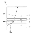
- It is sectional drawing which shows schematically the structure of the silicon carbide epitaxial substrate of a comparative example. It is a fragmentary sectional view showing a situation of extension of a basal plane dislocation in a silicon carbide epitaxial substrate at the time of bipolar operation of a silicon carbide semiconductor device of a comparative example.
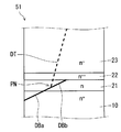
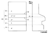
- FIG. 2 is a partial cross sectional view showing a state of elongation of basal plane dislocations in a silicon carbide epitaxial substrate during bipolar operation of silicon carbide semiconductor device of FIG. 1. It is sectional drawing which shows schematically the structure of the silicon carbide semiconductor device of the 1st modification in Embodiment 1 of this invention. It is sectional drawing which shows schematically the structure of the silicon carbide semiconductor device of the 2nd modification in Embodiment 1 of this invention. It is sectional drawing which shows schematically the structure of the silicon carbide epitaxial substrate in Embodiment 2 of this invention, and the figure which shows the typical impurity concentration profile. It is sectional drawing which shows schematically the structure of the silicon carbide epitaxial substrate in Embodiment 3 of this invention, and the figure which shows the typical impurity concentration profile.
- pin diode 100 (silicon carbide semiconductor device) of the present embodiment is manufactured using silicon carbide epitaxial substrate 51.
- the pin diode 100 has the silicon carbide epitaxial substrate 51.
- Silicon carbide epitaxial substrate 51 includes an n-type (one conductivity type) silicon carbide single crystal substrate 10, an n-type first silicon carbide layer 21, an n-type second silicon carbide layer 22, and an n-type.
- the third silicon carbide layer 23 (active layer).
- First silicon carbide layer 21 is provided on silicon carbide single crystal substrate 10.
- First silicon carbide layer 21 may be provided directly on silicon carbide single crystal substrate 10.
- Second silicon carbide layer 22 is provided on first silicon carbide layer 21.
- Second silicon carbide layer 22 may be provided directly on first silicon carbide layer 21.
- Third silicon carbide layer 23 is provided on second silicon carbide layer 22.
- Third silicon carbide layer 23 may be provided directly on second silicon carbide layer 22.
- First silicon carbide layer 21, second silicon carbide layer 22, and third silicon carbide layer 23 are epitaxial layers formed by epitaxial growth on silicon carbide single crystal substrate 10. Epitaxial growth can be performed by a CVD method.
- Silicon carbide single crystal substrate 10 has a first impurity concentration.
- the first impurity concentration is preferably 5 ⁇ 10 17 cm ⁇ 3 or more and 1 ⁇ 10 19 cm ⁇ 3 or less.
- First silicon carbide layer 21 has a second impurity concentration lower than the first impurity concentration.
- the second impurity concentration is such that the rate at which the basal plane dislocation DBa propagated from the silicon carbide single crystal substrate 10 during epitaxial growth is converted to the threading edge dislocation DT at the turning point PN in the first silicon carbide layer 21 is increased. Is preferably selected.
- the second impurity concentration is preferably 5 ⁇ 10 16 cm ⁇ 3 or more and 1 ⁇ 10 19 cm ⁇ 3 or less.
- Second silicon carbide layer 22 has a third impurity concentration higher than the first impurity concentration.
- the third impurity concentration is preferably 2 ⁇ 10 19 cm ⁇ 3 or less.
- the lower limit value of the third impurity concentration needs to be higher than the first impurity concentration, specifically 5 ⁇ 10 18 cm ⁇ 3 or more.
- Third silicon carbide layer 23 has a fourth impurity concentration lower than the first impurity concentration.
- the fourth impurity concentration is preferably lower than the second impurity concentration, specifically 1 ⁇ 10 14 cm ⁇ 3 or more and 5 ⁇ 10 16 cm ⁇ 3 or less, for example, 5 ⁇ 10 15 cm ⁇ .
- Silicon carbide single crystal substrate 10 has a hexagonal crystal structure, and preferably has crystal polymorph 4H.
- the surface (upper surface in the figure) on which silicon carbide single crystal substrate 10 is provided with first silicon carbide layer 21 has an off angle larger than 0 ° with respect to the ⁇ 0001 ⁇ plane.
- the off angle is preferably 0.05 ° or more, and more preferably 0.1 ° or more. By providing a certain amount of off-angle, it is easy to form an epitaxial layer having a crystal structure similar to the crystal structure of silicon carbide single crystal substrate 10.
- the off angle is preferably 8 ° or less, and more preferably 5 ° or less.
- the off angle is preferably an angle based on the (0001) plane among the (0001) plane and the (000-1) plane which are ⁇ 0001 ⁇ planes.
- the pin diode 100 further includes a p-type (conductivity type different from one conductivity type) fourth silicon carbide layer 124, a cathode electrode 101 (first electrode), an anode electrode 102 (second electrode), It has a JTE (Junction Termination Extension) region 123 and an insulating film 133.
- Fourth silicon carbide layer 124 is provided on third silicon carbide layer 23.
- Fourth silicon carbide layer 124 may be provided directly on third silicon carbide layer 23.
- Cathode electrode 101 is electrically connected to silicon carbide single crystal substrate 10.
- Cathode electrode 101 is ohmically connected to silicon carbide single crystal substrate 10. In order to obtain such a connection, the cathode electrode 101 may be provided directly on the silicon carbide single crystal substrate 10.
- the anode electrode 102 is electrically connected to the fourth silicon carbide layer 124.
- the anode electrode 102 is ohmically connected to the fourth silicon carbide layer 124. In order to obtain such a connection, the anode electrode 102 may be provided directly on the fourth silicon carbide layer 124.
- silicon carbide epitaxial substrate 59 of the comparative example as in silicon carbide epitaxial substrate 51 (FIG. 2), the extension of basal plane dislocation DBa during epitaxial growth occurs in first silicon carbide layer 21. Stopped at the turning point PN.
- silicon carbide epitaxial substrate 59 (FIG. 3) is not provided with second silicon carbide layer 22.
- the present inventors considered that a structure that prevents the extension of the basal plane dislocation from the basal plane dislocation DBa existing below the turning point PN is necessary in the epitaxial layer.
- the relationship between the extension of basal plane dislocations and the impurity concentration in silicon carbide was investigated, and it was found that the basal plane dislocations extended in the direction of lower impurity concentration.
- elongation of basal plane dislocations is suppressed in a region where the impurity concentration is high, and that elongation is substantially prevented particularly in a region where the impurity concentration is 5 ⁇ 10 18 cm ⁇ 3 or more.
- silicon carbide epitaxial substrate 51 (FIG. 2) according to the present embodiment is configured such that second silicon carbide layer 22 is provided on first silicon carbide layer 21.
- the impurity concentration (third impurity concentration) of second silicon carbide layer 22 is higher than the impurity concentration (first impurity concentration) of silicon carbide single crystal substrate 10, and preferably 5 ⁇ 10 18 cm ⁇ 3 or more. It was done.
- a silicon carbide epitaxial substrate having only a concentration gradient layer (similar to a buffer layer 29 (FIG. 8) described later) whose impurity concentration gradually decreases as an epitaxial layer immediately above the silicon carbide single crystal substrate 10.
- This silicon carbide epitaxial substrate was irradiated with an ultraviolet laser in order to cause pseudo energization deterioration.
- the stacking faults enlarged thereby were observed from the epitaxial growth surface side. As a result, the stacking fault width was narrower as the impurity concentration was higher.
- the reason why the high impurity concentration layer suppresses the expansion of basal plane dislocations is that the stacking faults (in other words, two partial dislocations bordering them) are difficult to move in the high impurity concentration layer. This is probably because of this. It is known that stacking faults are enlarged when one of the two partial dislocations, called a Si core, moves in the crystal. The partial dislocations in the Si core tend to move to a lower impurity concentration side. Therefore, the impurity concentration (third impurity concentration) of second silicon carbide layer 22 needs to be higher than the impurity concentration (first impurity concentration) of silicon carbide single crystal substrate 10, preferably 2 The impurity concentration is twice or more.
- the impurity concentration of the second silicon carbide layer 22 is preferably 2 ⁇ 10 19 cm ⁇ 3 or less.
- basal plane dislocation DBa in silicon carbide single crystal substrate 10 is the first carbonization during epitaxial growth for manufacturing silicon carbide epitaxial substrate 51 (FIG. 2).
- the silicon layer 21 converts the threading edge dislocation DT. This suppresses the propagation of basal plane dislocations into the third silicon carbide layer 23 during epitaxial growth.
- the first silicon carbide layer 21 to the third carbonized carbon during bipolar operation using the pin structure of the laminated structure of the fourth silicon carbide layer 124, the third silicon carbide layer 23, and the silicon carbide single crystal substrate 10.
- the extension of the basal plane dislocation DBb (FIG. 5) toward the silicon layer 23 is prevented by the second silicon carbide layer 22. Therefore, in the bipolar operation, it is possible to suppress energization deterioration due to the extension and expansion of the basal plane dislocation in the third silicon carbide layer 23.
- the cathode electrode 101 is electrically connected to the silicon carbide single crystal substrate 10, and the anode electrode 102 is electrically connected to the fourth silicon carbide layer 124.
- a vertical semiconductor device having the cathode electrode 101 and the anode electrode 102 as main electrodes is configured.
- deterioration of energization during bipolar operation tends to be a problem, and this embodiment can suppress this.
- the cathode electrode 101 is ohmically connected to the silicon carbide single crystal substrate 10, and the anode electrode 102 is ohmically connected to the fourth silicon carbide layer 124.
- cathode electrode 101 and anode electrode 102 are connected by a pin structure having a laminated structure of fourth silicon carbide layer 124, third silicon carbide layer 23, and silicon carbide single crystal substrate 10.
- the current deterioration has been easy to occur in the past, but this embodiment can suppress it.
- basal plane dislocation DBa in silicon carbide single crystal substrate 10 is the first silicon carbide layer during epitaxial growth for manufacturing silicon carbide epitaxial substrate 51. 21 is converted into a threading edge dislocation DT. This suppresses the propagation of basal plane dislocations into the third silicon carbide layer 23 during epitaxial growth. Further, during the bipolar operation of pin diode 100 (FIG. 1) using silicon carbide epitaxial substrate 51, the extension of basal plane dislocation DBb from first silicon carbide layer 21 toward third silicon carbide layer 23 is increased. It is obstructed by two silicon carbide layers 22. Therefore, in the bipolar operation, it is possible to suppress energization deterioration due to the extension and expansion of the basal plane dislocation in the third silicon carbide layer 23.
- the impurity concentration (fourth impurity concentration) of third silicon carbide layer 23 is lower than the impurity concentration (second impurity concentration) of first silicon carbide layer 21.
- the impurity concentration of third silicon carbide layer 23 can be sufficiently lowered. Therefore, the withstand voltage of pin diode 100 (FIG. 1) using silicon carbide epitaxial substrate 51 can be increased as compared with the case where the fourth impurity concentration is higher than the second impurity concentration.
- the impurity concentration (third impurity concentration) of second silicon carbide layer 22 is 2 ⁇ 10 19 cm ⁇ 3 or less. Thereby, generation
- the silicon carbide semiconductor device is not limited to the pin diode 100 (FIG. 1), and may be another bipolar device.
- MOSFET Metal Oxide Semiconductor Field Effect Transistor
- the MOSFET may be a planar gate type MOSFET 200 (FIG. 6).
- the planar gate MOSFET 200 (FIG.
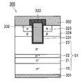
- the MOSFET may be a trench gate type MOSFET 300 (FIG. 7).
- the trench gate type MOSFET 300 includes a silicon carbide epitaxial substrate 51, a base layer 324 (fourth silicon carbide layer), a source layer 323, a gate insulating film 331, a gate electrode 332, a drain electrode 301 (first electrode). ) And a source electrode 302 (second electrode).
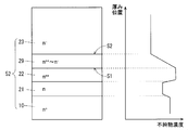
- silicon carbide epitaxial substrate 52 of the present embodiment has a buffer layer 29.
- the buffer layer 29 has a first surface S1 and a second surface S2 opposite to the first surface S1.
- Buffer layer 29 is made of silicon carbide. Buffer layer 29 may be formed by epitaxial growth on second silicon carbide layer 22.
- the first surface S 1 faces the second silicon carbide layer 22, and the second surface S 2 faces the third silicon carbide layer 23.
- First surface S ⁇ b> 1 may directly face second silicon carbide layer 22.
- Second surface S ⁇ b> 2 may directly face third silicon carbide layer 23.
- First surface S1 directly faces second silicon carbide layer 22 and second surface S2 directly faces third silicon carbide layer 23, so that third silicon carbide layer 23 is second Provided on silicon carbide layer 22 through buffer layer 29 only.
- the buffer layer 29 has an impurity concentration profile that continuously decreases from the first surface S1 toward the second surface S2.
- the impurity concentration profile of the buffer layer 29 is preferably linearly changed as shown in FIG. 8, but may not be linear unless accompanied by a steep change. Is done.
- the impurity concentration profile has a step structure that changes discontinuously (in other words, discretely)
- new crystal defects are likely to occur at the discontinuous interface during epitaxial growth. This is because at the interface where the impurity concentration is discontinuous, the lattice constant of the crystal also becomes discontinuous, resulting in distortion.
- the impurity concentration is reduced from about 1 ⁇ 10 18 cm ⁇ 3 per 1 ⁇ m thickness from the first surface S1 toward the second surface S2. Thereby, the change in the impurity concentration can be prevented from becoming steep at the interface between the buffer layer 29 and the third silicon carbide layer 23.
- the concentration change is not steep at other interfaces.
- the layers are preferably connected so that the impurity concentration changes smoothly. In this case, strictly speaking, not only between the second silicon carbide layer 22 and the third silicon carbide layer 23, but also between the silicon carbide single crystal substrate 10 and the first silicon carbide layer, and the first It can be said that a buffer layer (not shown in the cross-sectional view of FIG. 8) is also provided between each of the silicon carbide layer and the second silicon carbide layer.
- the buffer layer 29 suppresses a sharp change in the impurity concentration between the second silicon carbide layer 22 and the third silicon carbide layer 23. Thereby, it can suppress that a new crystal defect arises at the time of epitaxial growth. Therefore, the effect described in Embodiment 1 can be further enhanced. It is noted that a silicon carbide semiconductor device substantially similar to that in the first embodiment can be manufactured using silicon carbide epitaxial substrate 52.
- silicon carbide epitaxial substrate 53 of the present embodiment has a buffer layer 29v instead of buffer layer 29 of silicon carbide epitaxial substrate 52 of the second embodiment (FIG. 8). Similar to the buffer layer 29, the buffer layer 29v has a first surface S1 and a second surface S2 opposite to the first surface S1. Buffer layer 29v is made of silicon carbide. Buffer layer 29v can be formed by epitaxial growth on second silicon carbide layer 22.
- the first surface S1 faces the second silicon carbide layer 22, and the second surface S2 faces the third silicon carbide layer 23.
- First surface S ⁇ b> 1 may directly face second silicon carbide layer 22.
- Second surface S ⁇ b> 2 may directly face third silicon carbide layer 23.
- First surface S1 directly faces second silicon carbide layer 22 and second surface S2 directly faces third silicon carbide layer 23, so that third silicon carbide layer 23 is second Provided on silicon carbide layer 22 only through buffer layer 29v.
- the buffer layer 29v has an impurity concentration profile that continuously decreases from the first surface S1 toward the second surface S2.
- a point between the first surface S1 and the second surface S2 is defined as an intermediate point PI.
- the intermediate point PI may be a point located between the first surface S1 and the second surface S2 and away from each of the first surface S1 and the second surface S2, and the first surface S1. And it is not necessary to be located equidistant from the second surface S2.
- the buffer layer 29v has its impurity concentration continuously decreased from the first surface S1 toward the intermediate point PI at the first decrease rate, and from the intermediate point PI to the second point.
- the impurity concentration profile continuously decreases toward the surface S2 at the second decrease rate.
- the first reduction rate is smaller than the second reduction rate.
- the buffer layer 29v has a thickness in the thickness direction of the buffer layer 29v from directly above the second silicon carbide layer 22.
- the change in the impurity concentration up to the intermediate point PI is made more gradual. Thereby, the generation of strain at the interface between second silicon carbide layer 22 and third silicon carbide layer 23 is suppressed. Therefore, generation of new crystal defects can be further suppressed.
- the buffer layer 29v is formed as follows, for example. First, the first silicon carbide having a thickness of 10 ⁇ m is formed on the second silicon carbide layer 22 so that the impurity concentration decreases toward the surface at 2 ⁇ 10 17 cm ⁇ 3 (first reduction rate) per 1 ⁇ m thickness. Regions are deposited. A second silicon carbide region having a thickness of 5 ⁇ m is deposited on the first silicon carbide region so that the impurity concentration decreases toward the surface at 2 ⁇ 10 18 cm ⁇ 3 (second reduction rate) per 1 ⁇ m thickness. Is done. Thereby, buffer layer 29v having a total thickness of 15 ⁇ m is formed, and the position of the interface between the first silicon carbide region and the second silicon carbide region corresponds to intermediate point PI.
- the intermediate point PI corresponds to a point where the impurity concentration profile is bent.
- the intermediate point PI does not necessarily need to be such a point, and may be virtually determined so that the impurity concentration profile satisfies the above-described conditions.
- each of the first and second reduction rates is constant, but these may vary in the thickness direction.
- the impurity concentration profile does not necessarily change in a straight line, and may change in a curve.
- each of the first and second reduction rates may be represented by an average value.
- Example 1 As silicon carbide single crystal substrate 10 (FIG. 2), a silicon carbide substrate having an off angle of 4 degrees, a diameter of 75 mm (3 inches), a crystal polymorph 4H, a conductivity type n type, and an impurity concentration of 5 ⁇ 10 18 cm ⁇ 3 is prepared. It was done. The surface of the silicon carbide substrate was previously processed into a mirror surface by mechanical polishing and chemical mechanical polishing. The basal plane dislocation density on the surface was 500 cm ⁇ 2 .
- silicon carbide single crystal substrate 10 was immersed in a heated mixed solution of ammonia water and hydrogen peroxide water.
- silicon carbide single crystal substrate 10 was immersed in a mixed solution of heated hydrochloric acid and hydrogen peroxide.
- silicon carbide single crystal substrate 10 was immersed in an aqueous solution containing hydrogen fluoride.
- a replacement treatment with pure water was performed.
- silicon carbide single crystal substrate 10 was dried.
- foreign matters such as metal elements may be present on the surface before the surface cleaning. Such foreign matters can cause new crystal defects during epitaxial growth.
- hydrogen gas introduced in the first stage of epitaxial growth described later also has an effect of removing surface contamination.
- foreign matters on the surface are removed before the silicon carbide single crystal substrate 10 is introduced into the reactor for epitaxial growth, for the purpose of sufficiently cleaning the surface and maintaining the cleanliness in the growth furnace. It is desirable to keep it.
- silicon carbide single crystal substrate 10 was introduced into a reaction furnace of a CVD apparatus for epitaxial growth.
- the temperature in the reaction furnace was 1575 ° C.
- Epitaxial growth was started by introducing a silicon carbide source gas and an impurity source gas after starting to supply hydrogen gas as a carrier gas.
- the first silicon carbide layer 21 having an impurity concentration of 5 ⁇ 10 17 cm ⁇ 3 was formed with a thickness of 500 nm.
- the second silicon carbide layer 22 having an impurity concentration of 1 ⁇ 10 19 cm ⁇ 3 was formed with a thickness of 1 ⁇ m by adjusting the nitrogen gas flow rate.
- a third silicon carbide layer 23 having an impurity concentration of 3 ⁇ 10 16 cm ⁇ 3 was formed with a thickness of 10 ⁇ m.
- Monosilane and propane were used as the silicon carbide source gas.
- the impurity source gas a gas containing nitrogen (N) atoms, specifically nitrogen gas, was used. Instead of nitrogen gas, a gas containing phosphorus (P) atoms can also be used.
- N nitrogen
- P phosphorus
- the epitaxial layer to be grown is p-type, a gas containing aluminum (Al) atoms or boron (B) atoms can be used.
- silicon carbide epitaxial substrate 51 was obtained.
- the basal plane dislocation density in the third silicon carbide layer 23 was 300 cm ⁇ 2 .
- a pin diode 100 (FIG. 1), which is a bipolar element, was fabricated.
- an element having no basal plane dislocation in the third silicon carbide layer 23 as the active layer was selected.
- the device was subjected to forward energization for 60 minutes at a current density of 50 Acm ⁇ 2 . As a result, there was no change in the characteristics of the diode.
- basal plane dislocation was observed for the element in which the basal plane dislocation exists in the third silicon carbide layer 23 as the active layer.
- basal plane dislocations were formed from the interface between the second silicon carbide layer 22 and the third silicon carbide layer 23.
- Example 2 An epitaxial growth layer was formed on silicon carbide single crystal substrate 10 (FIG. 8) prepared in the same manner as in Example 1. Specifically, first, growth was started with the nitrogen gas flow rate adjusted so that the impurity concentration was 5 ⁇ 10 18 cm ⁇ 3 . By decreasing the nitrogen gas flow rate at a constant rate at the same time as the growth starts, the impurity concentration linearly decreases from 5 ⁇ 10 18 cm ⁇ 3 to 5 ⁇ 10 17 cm ⁇ 3 on the silicon carbide single crystal substrate 10. Such a buffer layer was formed with a thickness of 200 nm. Subsequently, a first silicon carbide layer 21 having an impurity concentration of 5 ⁇ 10 17 cm ⁇ 3 was formed.
- the second silicon carbide layer 22 was formed with a thickness of 500 nm. Further, a buffer layer 29 having a thickness of 10 ⁇ m was formed so that the impurity concentration decreased linearly from 5 ⁇ 10 19 cm ⁇ 3 to 3 ⁇ 10 16 cm ⁇ 3 . A third silicon carbide layer 23 having an impurity concentration of 3 ⁇ 10 16 cm ⁇ 3 was formed on buffer layer 29 to a thickness of 10 ⁇ m.
- silicon carbide epitaxial substrate 52 was obtained.
- the basal plane dislocation density in the third silicon carbide layer 23 was 50 cm ⁇ 2 .
- the basal plane dislocations were propagated from the silicon carbide single crystal substrate 10.
- a pin diode which is a bipolar element, was fabricated.
- an element having no basal plane dislocation in the third silicon carbide layer 23 as the active layer was selected.
- the device was subjected to forward energization for 60 minutes at a current density of 50 Acm ⁇ 2 . As a result, there was no change in the characteristics of the diode.
- An epitaxial growth layer was formed on silicon carbide single crystal substrate 10 (FIG. 3) prepared in the same manner as in Example 1. Specifically, first, a first silicon carbide layer 21 having an impurity concentration of 5 ⁇ 10 17 cm ⁇ 3 was formed with a thickness of 500 nm. Subsequently, by adjusting the nitrogen gas flow rate, a third silicon carbide layer 23 having an impurity concentration of 3 ⁇ 10 16 cm ⁇ 3 was formed to a thickness of 10 ⁇ m. Thus, silicon carbide epitaxial substrate 59 was obtained. When the entire photoluminescence image was acquired, the basal plane dislocation density in the third silicon carbide layer 23 was 100 cm ⁇ 2 . Using this silicon carbide epitaxial substrate 59, a pin diode, which is a bipolar element, was fabricated.
- an element having no basal plane dislocation in the third silicon carbide layer 23 as the active layer was selected.
- the device was subjected to forward energization for 60 minutes at a current density of 50 Acm ⁇ 2 .
- the forward voltage drop increased with energization.
- the photo-luminescence image was acquired.
- enlarged stacking faults were confirmed.
- silicon carbide single crystal in first silicon carbide layer 21 FIG. 4).
- the basal plane dislocation DBa propagating from the crystal substrate 10 is converted into the threading edge dislocation DT, and the basal plane dislocation DBa (that is, stacking fault) below the conversion point PN is transferred to the third silicon carbide layer 23. It was observed that the basal plane dislocation DBz was extended.
Landscapes
- Chemical & Material Sciences (AREA)
- Engineering & Computer Science (AREA)
- Crystallography & Structural Chemistry (AREA)
- Materials Engineering (AREA)
- Metallurgy (AREA)
- Organic Chemistry (AREA)
- Chemical Kinetics & Catalysis (AREA)
- General Chemical & Material Sciences (AREA)
- Inorganic Chemistry (AREA)
- Recrystallisation Techniques (AREA)
- Crystals, And After-Treatments Of Crystals (AREA)
- Chemical Vapour Deposition (AREA)
Abstract
Description
図1および図2を参照して、本実施の形態のpinダイオード100(炭化珪素半導体装置)は、炭化珪素エピタキシャル基板51を用いて製造されたものである。言い換えれば、pinダイオード100は炭化珪素エピタキシャル基板51を有している。炭化珪素エピタキシャル基板51は、n型(一の導電型)の炭化珪素単結晶基板10と、n型の第1の炭化珪素層21と、n型の第2の炭化珪素層22と、n型の第3の炭化珪素層23(活性層)とを有している。第1の炭化珪素層21は炭化珪素単結晶基板10上に設けられている。第1の炭化珪素層21は炭化珪素単結晶基板10上に直接設けられていてよい。第2の炭化珪素層22は第1の炭化珪素層21上に設けられている。第2の炭化珪素層22は第1の炭化珪素層21上に直接設けられていてよい。第3の炭化珪素層23は第2の炭化珪素層22上に設けられている。第3の炭化珪素層23は第2の炭化珪素層22上に直接設けられていてよい。第1の炭化珪素層21、第2の炭化珪素層22および第3の炭化珪素層23は、炭化珪素単結晶基板10上のエピタキシャル成長によって形成されたエピタキシャル層である。エピタキシャル成長はCVD法によって行われ得る。
図8を参照して、本実施の形態の炭化珪素エピタキシャル基板52はバッファ層29を有している。バッファ層29は、第1の面S1と、第1の面S1と反対の第2の面S2とを有している。バッファ層29は炭化珪素から作られている。バッファ層29は、第2の炭化珪素層22上でのエピタキシャル成長によって形成され得る。
図9を参照して、本実施の形態の炭化珪素エピタキシャル基板53は、実施の形態2(図8)における炭化珪素エピタキシャル基板52のバッファ層29に代わり、バッファ層29vを有している。バッファ層29と同様、バッファ層29vは、第1の面S1と、第1の面S1と反対の第2の面S2とを有している。バッファ層29vは炭化珪素から作られている。バッファ層29vは、第2の炭化珪素層22上でのエピタキシャル成長によって形成され得る。
(実施例1)
炭化珪素単結晶基板10(図2)として、オフ角4度、直径75mm(3インチ)、結晶多形4H、導電型n型、不純物濃度5×1018cm-3を有する炭化珪素基板が用意された。炭化珪素基板の表面は、あらかじめ、機械研磨および化学機械研磨により鏡面に加工されていた。表面における基底面転位密度は500個cm-2であった。
実施例1と同様に準備された炭化珪素単結晶基板10(図8)上に、エピタキシャル成長層が形成された。具体的には、まず、不純物濃度が5×1018cm-3となるように窒素ガス流量を調整された状態で成長が開始された。成長が始まると同時に窒素ガス流量を一定の割合で減少させることで、炭化珪素単結晶基板10上に、不純物濃度が5×1018cm-3から5×1017cm-3まで線形に減少するようなバッファ層が200nmの厚みで形成された。続いて、不純物濃度が5×1017cm-3の第1の炭化珪素層21が形成された。次に、不純物濃度が5×1017cm-3から1×1019cm-3まで線形に増加するようなバッファ層を500nmの厚みで成長させた後に、不純物濃度が1×1019cm-3の第2の炭化珪素層22が500nmの厚みで形成された。さらに、不純物濃度が5×1019cm-3から3×1016cm-3まで線形に減少するようなバッファ層29が10μmの厚みで形成された。バッファ層29上に不純物濃度が3×1016cm-3の第3の炭化珪素層23が10μmの厚みで形成された。
実施例1と同様に準備された炭化珪素単結晶基板10(図3)上に、エピタキシャル成長層が形成された。具体的には、まず、不純物濃度5×1017cm-3の第1の炭化珪素層21が500nmの厚みで形成された。続いて、窒素ガス流量を調整することで、不純物濃度が3×1016cm-3の第3の炭化珪素層23が10μmの厚みで形成された。以上により、炭化珪素エピタキシャル基板59を得た。その全体のフォトルミネッセンスイメージを取得したところ、第3の炭化珪素層23中の基底面転位密度は100個cm-2であった。この炭化珪素エピタキシャル基板59を用いて、バイポーラ素子であるpinダイオードが作製された。
Claims (10)
- 第1の不純物濃度を有する一の導電型の炭化珪素単結晶基板(10)と、
前記炭化珪素単結晶基板(10)上に設けられ、前記第1の不純物濃度よりも低い第2の不純物濃度を有する前記一の導電型の第1の炭化珪素層(21)と、
前記第1の炭化珪素層(21)上に設けられ、前記第1の不純物濃度よりも高い第3の不純物濃度を有する前記一の導電型の第2の炭化珪素層(22)と、
前記第2の炭化珪素層(22)上に設けられ、前記第2の不純物濃度よりも低い第4の不純物濃度を有する前記一の導電型の第3の炭化珪素層(23)と、
を備える、炭化珪素エピタキシャル基板(51~53)。 - 前記第3の不純物濃度は2×1019cm-3以下である、請求項1に記載の炭化珪素エピタキシャル基板(51~53)。
- 前記第3の不純物濃度は5×1018cm-3以上である、請求項1または2に記載の炭化珪素エピタキシャル基板(51~53)。
- 前記第2の不純物濃度は5×1016cm-3以上、1×1019cm-3以下である、請求項1から3のいずれか1項に記載の炭化珪素エピタキシャル基板(51~53)。
- 前記第4の不純物濃度は1×1014cm-3以上、5×1016cm-3以下である、請求項1から4のいずれか1項に記載の炭化珪素エピタキシャル基板(51~53)。
- 第1の面(S1)と前記第1の面(S1)と反対の第2の面(S2)とを有し、炭化珪素から作られたバッファ層(29,29v)をさらに備え、
前記第1の面(S1)は前記第2の炭化珪素層(22)に面しており、前記第2の面(S2)は前記第3の炭化珪素層(23)に面しており、前記バッファ層(29,29v)は、前記第1の面(S1)から前記第2の面(S2)へ向かって連続的に減少する不純物濃度プロファイルを有している、請求項1から5のいずれか1項に記載の炭化珪素エピタキシャル基板(51~53)。 - 第1の面(S1)と前記第1の面(S1)と反対の第2の面(S2)とを有し、炭化珪素から作られたバッファ層(29v)をさらに備え、
前記第1の面(S1)は前記第2の炭化珪素層(22)に面しており、前記第2の面(S2)は前記第3の炭化珪素層(23)に面しており、
前記バッファ層(29v)の前記第1の面(S1)と前記第2の面(S2)との間の地点を中間地点とすると、前記バッファ層(29v)は、不純物濃度が、前記第1の面(S1)から前記中間地点へ向かって連続的に第1の減少率で減少し、かつ前記中間地点から前記第2の面(S2)へ向かって第2の減少率で連続的に減少する不純物濃度プロファイルを有しており、
前記第1の減少率は前記第2の減少率よりも小さい、
請求項1から5のいずれか1項に記載の炭化珪素エピタキシャル基板(53)。 - 第1の不純物濃度を有する一の導電型の炭化珪素単結晶基板(10)と、
前記炭化珪素単結晶基板(10)上に設けられ、前記第1の不純物濃度よりも低い第2の不純物濃度を有する前記一の導電型の第1の炭化珪素層(21)と、
前記第1の炭化珪素層(21)上に設けられ、前記第1の不純物濃度よりも高い第3の不純物濃度を有する前記一の導電型の第2の炭化珪素層(22)と、
前記第2の炭化珪素層(22)上に設けられ、前記第2の不純物濃度よりも低い第4の不純物濃度を有する前記一の導電型の第3の炭化珪素層(23)と、
前記第3の炭化珪素層(23)上に設けられた、前記一の導電型と異なる導電型の第4の炭化珪素層(124,224,324)と、
を備える、炭化珪素半導体装置(100,200,300)。 - 前記炭化珪素単結晶基板(10)に電気的に接続された第1の電極(101,201,301)と、
前記第4の炭化珪素層(124,224,324)に電気的に接続された第2の電極(102,202,302)と、
をさらに備える、請求項8に記載の炭化珪素半導体装置(100,200,300)。 - 前記第1の電極(101,201,301)は前記炭化珪素単結晶基板(10)にオーミック接続されており、前記第2の電極(102,202,302)は前記第4の炭化珪素層(124,224,324)にオーミック接続されている、請求項9に記載の炭化珪素半導体装置(100,200,300)。
Priority Applications (6)
| Application Number | Priority Date | Filing Date | Title |
|---|---|---|---|
| DE112016004194.2T DE112016004194B4 (de) | 2015-12-02 | 2016-11-30 | Epitaxiales Substrat aus Siliciumcarbid und Siliciumcarbid-Halbleitereinrichtung |
| JP2017554137A JP6351874B2 (ja) | 2015-12-02 | 2016-11-30 | 炭化珪素エピタキシャル基板および炭化珪素半導体装置 |
| US15/749,621 US10415154B2 (en) | 2015-12-02 | 2016-11-30 | Silicon carbide epitaxial substrate and silicon carbide semiconductor device |
| CN201680051471.2A CN108292686B (zh) | 2015-12-02 | 2016-11-30 | 碳化硅外延基板及碳化硅半导体装置 |
| US16/375,455 US10774441B2 (en) | 2015-12-02 | 2019-04-04 | Silicon carbide epitaxial substrate and silicon carbide semiconductor device |
| US16/871,440 US10995420B2 (en) | 2015-12-02 | 2020-05-11 | Silicon carbide epitaxial substrate and silicon carbide semiconductor device |
Applications Claiming Priority (2)
| Application Number | Priority Date | Filing Date | Title |
|---|---|---|---|
| JP2015-235372 | 2015-12-02 | ||
| JP2015235372 | 2015-12-02 |
Related Child Applications (2)
| Application Number | Title | Priority Date | Filing Date |
|---|---|---|---|
| US15/749,621 A-371-Of-International US10415154B2 (en) | 2015-12-02 | 2016-11-30 | Silicon carbide epitaxial substrate and silicon carbide semiconductor device |
| US16/375,455 Division US10774441B2 (en) | 2015-12-02 | 2019-04-04 | Silicon carbide epitaxial substrate and silicon carbide semiconductor device |
Publications (1)
| Publication Number | Publication Date |
|---|---|
| WO2017094764A1 true WO2017094764A1 (ja) | 2017-06-08 |
Family
ID=58796951
Family Applications (1)
| Application Number | Title | Priority Date | Filing Date |
|---|---|---|---|
| PCT/JP2016/085525 Ceased WO2017094764A1 (ja) | 2015-12-02 | 2016-11-30 | 炭化珪素エピタキシャル基板および炭化珪素半導体装置 |
Country Status (5)
| Country | Link |
|---|---|
| US (3) | US10415154B2 (ja) |
| JP (1) | JP6351874B2 (ja) |
| CN (1) | CN108292686B (ja) |
| DE (1) | DE112016004194B4 (ja) |
| WO (1) | WO2017094764A1 (ja) |
Cited By (25)
| Publication number | Priority date | Publication date | Assignee | Title |
|---|---|---|---|---|
| WO2018123148A1 (ja) * | 2016-12-27 | 2018-07-05 | 住友電気工業株式会社 | 炭化珪素エピタキシャル基板および炭化珪素半導体装置の製造方法 |
| DE102018130046A1 (de) | 2017-12-06 | 2019-06-06 | Showa Denko K. K. | BEWERTUNGSVERFAHREN UND HERSTELLUNGSVERFAHREN VON SiC-EPITAXIALWAFERN |
| JP2019153743A (ja) * | 2018-03-06 | 2019-09-12 | 株式会社東芝 | 半導体装置、基板、半導体装置の製造方法、及び、基板の製造方法 |
| JP2020068241A (ja) * | 2018-10-22 | 2020-04-30 | 株式会社東芝 | 半導体装置、基板、及び、半導体装置の製造方法 |
| DE102019129273A1 (de) | 2018-11-09 | 2020-05-14 | Showa Denko K.K. | Verfahren zur Herstellung eines SiC-Epitaxiewafers |
| JP2020077720A (ja) * | 2018-11-06 | 2020-05-21 | 富士電機株式会社 | 炭化珪素半導体装置および炭化珪素半導体装置の製造方法 |
| WO2020115951A1 (ja) * | 2018-12-04 | 2020-06-11 | 住友電気工業株式会社 | 炭化珪素エピタキシャル基板および炭化珪素半導体装置 |
| JP2020096004A (ja) * | 2018-12-10 | 2020-06-18 | 株式会社東芝 | 半導体装置、基板、及び、半導体装置の製造方法。 |
| JP2021088469A (ja) * | 2019-12-02 | 2021-06-10 | 株式会社デンソー | 炭化珪素単結晶およびその製造方法 |
| JP2021187697A (ja) * | 2020-05-28 | 2021-12-13 | 住友金属鉱山株式会社 | 炭化珪素単結晶基板の製造方法 |
| CN114430782A (zh) * | 2019-09-27 | 2022-05-03 | 东海炭素株式会社 | 一种多晶SiC成型体 |
| CN114514342A (zh) * | 2019-09-27 | 2022-05-17 | 东海炭素株式会社 | 一种多晶SiC成型体及其制造方法 |
| JP2022122034A (ja) * | 2021-02-09 | 2022-08-22 | 富士電機株式会社 | 炭化珪素半導体装置および炭化珪素半導体装置の製造方法 |
| JP7187620B1 (ja) | 2021-07-13 | 2022-12-12 | 昭和電工株式会社 | SiCエピタキシャルウェハ及びSiCエピタキシャルウェハの製造方法 |
| JP7216248B1 (ja) | 2021-07-13 | 2023-01-31 | 昭和電工株式会社 | SiCデバイス及びSiCデバイスの製造方法 |
| JPWO2023032455A1 (ja) * | 2021-09-03 | 2023-03-09 | ||
| JP2023043833A (ja) * | 2021-09-16 | 2023-03-29 | 株式会社プロテリアル | 炭化ケイ素基板およびその製造方法 |
| JP2023095359A (ja) * | 2021-12-24 | 2023-07-06 | 株式会社デンソー | 炭化珪素ウェハおよびその製造方法 |
| WO2024058044A1 (ja) * | 2022-09-13 | 2024-03-21 | 住友電気工業株式会社 | 炭化珪素エピタキシャル基板、エピタキシャル基板の製造方法および炭化珪素半導体装置の製造方法 |
| JP2024103227A (ja) * | 2023-01-20 | 2024-08-01 | 株式会社デンソー | ダイオード、ダイオードを内蔵する電界効果トランジスタ、及びダイオードの製造方法 |
| JP2024110237A (ja) * | 2023-02-02 | 2024-08-15 | 株式会社東芝 | 半導体装置及びその製造方法 |
| US12166087B2 (en) | 2020-11-12 | 2024-12-10 | Resonac Corporation | SiC epitaxial wafer and method for manufacturing SIC epitaxial wafer |
| WO2024252795A1 (ja) * | 2023-06-08 | 2024-12-12 | 住友電気工業株式会社 | 炭化珪素基板、炭化珪素半導体装置および炭化珪素基板の製造方法 |
| WO2025004788A1 (ja) * | 2023-06-28 | 2025-01-02 | 住友電気工業株式会社 | 炭化珪素エピタキシャル基板、炭化珪素半導体装置の製造方法、および炭化珪素半導体装置 |
| WO2025017980A1 (ja) * | 2023-07-18 | 2025-01-23 | 株式会社 東芝 | 半導体基板、半導体装置及びその製造方法 |
Families Citing this family (16)
| Publication number | Priority date | Publication date | Assignee | Title |
|---|---|---|---|---|
| WO2017104751A1 (ja) * | 2015-12-18 | 2017-06-22 | 富士電機株式会社 | 炭化珪素半導体基板、炭化珪素半導体基板の製造方法、半導体装置および半導体装置の製造方法 |
| DE112017002020B4 (de) * | 2016-04-14 | 2023-03-02 | National Institute Of Advanced Industrial Science And Technology | Siliziumkarbid-halbleitervorrichtung und verfahren zur herstellung derselben |
| JP6743905B2 (ja) * | 2016-11-28 | 2020-08-19 | 三菱電機株式会社 | 炭化珪素半導体ウエハ、炭化珪素半導体チップ、および炭化珪素半導体装置の製造方法 |
| CN110301034B (zh) * | 2017-02-20 | 2023-07-11 | 株式会社博迈立铖 | 碳化硅层叠基板及其制造方法 |
| JP7447392B2 (ja) * | 2018-09-10 | 2024-03-12 | 株式会社レゾナック | SiC基板の評価方法及びSiCエピタキシャルウェハの製造方法 |
| JP7055725B2 (ja) * | 2018-09-14 | 2022-04-18 | 株式会社東芝 | 半導体装置 |
| IT201800010396A1 (it) * | 2018-11-16 | 2020-05-16 | St Microelectronics Srl | Sistema e metodo per la rilevazione della concentrazione di particelle metalliche |
| CN109904152A (zh) * | 2019-01-24 | 2019-06-18 | 江苏东海半导体科技有限公司 | 集成肖特基二极管的沟槽mosfet的制备方法 |
| JP7023882B2 (ja) * | 2019-02-04 | 2022-02-22 | 株式会社東芝 | 半導体装置の製造方法、基板の製造方法、半導体装置、基板、及び、基板の製造装置 |
| CN111599858B (zh) * | 2019-12-24 | 2021-08-20 | 湖南大学 | 一种抑制dv/dt,di/dt噪音产生的高压SiC IGBT的结构 |
| JP7361634B2 (ja) * | 2020-03-02 | 2023-10-16 | 三菱電機株式会社 | 半導体装置及び半導体装置の製造方法 |
| JPWO2022153918A1 (ja) * | 2021-01-15 | 2022-07-21 | ||
| JP7479315B2 (ja) * | 2021-03-08 | 2024-05-08 | 三菱電機株式会社 | 半導体装置および半導体装置の製造方法 |
| US20230084128A1 (en) * | 2021-09-16 | 2023-03-16 | Hitachi Metals, Ltd. | Silicon carbide substrate and method of manufacturing the same |
| CN114864529B (zh) * | 2022-05-18 | 2024-07-19 | 北京青禾晶元半导体科技有限责任公司 | 一种碳化硅复合基板及其制造方法与应用 |
| CN115394893A (zh) * | 2022-09-27 | 2022-11-25 | 广东省大湾区集成电路与系统应用研究院 | 半导体衬底的形成方法、半导体衬底及半导体激光器 |
Citations (6)
| Publication number | Priority date | Publication date | Assignee | Title |
|---|---|---|---|---|
| JP2000319099A (ja) * | 1999-05-07 | 2000-11-21 | Hiroyuki Matsunami | SiCウエハ、SiC半導体デバイス、および、SiCウエハの製造方法 |
| JP2009064970A (ja) * | 2007-09-06 | 2009-03-26 | Toshiba Corp | 半導体装置 |
| JP2011114252A (ja) * | 2009-11-30 | 2011-06-09 | Toshiba Corp | 半導体装置 |
| WO2012026234A1 (ja) * | 2010-08-24 | 2012-03-01 | 三菱電機株式会社 | エピタキシャルウエハ及び半導体装置 |
| WO2015170500A1 (ja) * | 2014-05-08 | 2015-11-12 | 三菱電機株式会社 | SiCエピタキシャルウエハおよび炭化珪素半導体装置の製造方法 |
| WO2016092887A1 (ja) * | 2014-12-12 | 2016-06-16 | 三菱電機株式会社 | 炭化珪素エピタキシャル基板および炭化珪素半導体装置 |
Family Cites Families (32)
| Publication number | Priority date | Publication date | Assignee | Title |
|---|---|---|---|---|
| DE10207522B4 (de) * | 2001-02-23 | 2018-08-02 | Fuji Electric Co., Ltd. | Halbleiterbauelement und Verfahren zu dessen Herstellung |
| JP4539011B2 (ja) * | 2002-02-20 | 2010-09-08 | 富士電機システムズ株式会社 | 半導体装置 |
| DE10360574B4 (de) * | 2003-12-22 | 2008-11-27 | Infineon Technologies Ag | Leistungshalbleiterbauelement mit sanftem Abschaltverhalten |
| US7528040B2 (en) * | 2005-05-24 | 2009-05-05 | Cree, Inc. | Methods of fabricating silicon carbide devices having smooth channels |
| DE102005046707B3 (de) * | 2005-09-29 | 2007-05-03 | Siced Electronics Development Gmbh & Co. Kg | SiC-PN-Leistungsdiode |
| JP2007250693A (ja) | 2006-03-14 | 2007-09-27 | Mitsubishi Materials Corp | SiC基板の製造方法及びSiC基板並びに半導体装置 |
| US7538412B2 (en) * | 2006-06-30 | 2009-05-26 | Infineon Technologies Austria Ag | Semiconductor device with a field stop zone |
| JP4937685B2 (ja) | 2006-09-21 | 2012-05-23 | 新日本製鐵株式会社 | エピタキシャル炭化珪素単結晶基板及びその製造方法 |
| JP5147244B2 (ja) | 2007-01-17 | 2013-02-20 | 関西電力株式会社 | バイポーラ型半導体素子 |
| JP5530602B2 (ja) | 2008-04-09 | 2014-06-25 | ルネサスエレクトロニクス株式会社 | 半導体装置およびその製造方法 |
| JP5458509B2 (ja) * | 2008-06-04 | 2014-04-02 | 日立金属株式会社 | 炭化珪素半導体基板 |
| JP5569532B2 (ja) * | 2009-11-02 | 2014-08-13 | 富士電機株式会社 | 半導体装置および半導体装置の製造方法 |
| JP4880052B2 (ja) | 2010-05-11 | 2012-02-22 | 新日本製鐵株式会社 | エピタキシャル炭化珪素単結晶基板及びその製造方法 |
| SE1051137A1 (sv) | 2010-10-29 | 2012-04-30 | Fairchild Semiconductor | Förfarande för tillverkning av en kiselkarbid bipolär transistor och kiselkarbid bipolär transistor därav |
| US8772788B2 (en) * | 2011-05-30 | 2014-07-08 | Panasonic Corporation | Semiconductor element and method of manufacturing thereof |
| JP2012253108A (ja) * | 2011-06-01 | 2012-12-20 | Sumitomo Electric Ind Ltd | 炭化珪素半導体装置およびその製造方法 |
| JP5869291B2 (ja) * | 2011-10-14 | 2016-02-24 | 富士電機株式会社 | 半導体装置 |
| WO2013089256A1 (ja) * | 2011-12-15 | 2013-06-20 | 富士電機株式会社 | 半導体装置および半導体装置の製造方法 |
| CN104620391B (zh) * | 2012-10-23 | 2017-09-19 | 富士电机株式会社 | 半导体装置及其制造方法 |
| JP2015053462A (ja) * | 2013-08-06 | 2015-03-19 | 住友電気工業株式会社 | 炭化珪素半導体装置およびその製造方法 |
| CN103474478A (zh) * | 2013-09-17 | 2013-12-25 | 西安电子科技大学 | 一种碳化硅sbd器件 |
| US9373710B2 (en) * | 2014-05-15 | 2016-06-21 | Infineon Technologies Ag | Insulated gate bipolar transistor |
| US9577045B2 (en) * | 2014-08-04 | 2017-02-21 | Fairchild Semiconductor Corporation | Silicon carbide power bipolar devices with deep acceptor doping |
| US9543427B2 (en) * | 2014-09-04 | 2017-01-10 | Panasonic Intellectual Property Management Co., Ltd. | Semiconductor device and method for fabricating the same |
| JP6392604B2 (ja) * | 2014-09-24 | 2018-09-19 | 国立大学法人京都大学 | ゲートドライバ |
| JP6457363B2 (ja) * | 2015-09-11 | 2019-01-23 | 株式会社東芝 | 半導体装置 |
| JP2017168666A (ja) * | 2016-03-16 | 2017-09-21 | 株式会社東芝 | 半導体装置 |
| JP6508099B2 (ja) * | 2016-03-18 | 2019-05-08 | 三菱電機株式会社 | 半導体素子 |
| US11075264B2 (en) * | 2016-05-31 | 2021-07-27 | Cree, Inc. | Super junction power semiconductor devices formed via ion implantation channeling techniques and related methods |
| DE102016112721B4 (de) * | 2016-07-12 | 2022-02-03 | Infineon Technologies Ag | n-Kanal-Leistungshalbleitervorrichtung mit p-Schicht im Driftvolumen |
| JP6946764B2 (ja) * | 2017-06-09 | 2021-10-06 | 富士電機株式会社 | 半導体装置および半導体装置の製造方法 |
| JP6815285B2 (ja) * | 2017-06-26 | 2021-01-20 | 株式会社東芝 | 半導体装置 |
-
2016
- 2016-11-30 CN CN201680051471.2A patent/CN108292686B/zh active Active
- 2016-11-30 WO PCT/JP2016/085525 patent/WO2017094764A1/ja not_active Ceased
- 2016-11-30 JP JP2017554137A patent/JP6351874B2/ja active Active
- 2016-11-30 US US15/749,621 patent/US10415154B2/en active Active
- 2016-11-30 DE DE112016004194.2T patent/DE112016004194B4/de active Active
-
2019
- 2019-04-04 US US16/375,455 patent/US10774441B2/en active Active
-
2020
- 2020-05-11 US US16/871,440 patent/US10995420B2/en active Active
Patent Citations (6)
| Publication number | Priority date | Publication date | Assignee | Title |
|---|---|---|---|---|
| JP2000319099A (ja) * | 1999-05-07 | 2000-11-21 | Hiroyuki Matsunami | SiCウエハ、SiC半導体デバイス、および、SiCウエハの製造方法 |
| JP2009064970A (ja) * | 2007-09-06 | 2009-03-26 | Toshiba Corp | 半導体装置 |
| JP2011114252A (ja) * | 2009-11-30 | 2011-06-09 | Toshiba Corp | 半導体装置 |
| WO2012026234A1 (ja) * | 2010-08-24 | 2012-03-01 | 三菱電機株式会社 | エピタキシャルウエハ及び半導体装置 |
| WO2015170500A1 (ja) * | 2014-05-08 | 2015-11-12 | 三菱電機株式会社 | SiCエピタキシャルウエハおよび炭化珪素半導体装置の製造方法 |
| WO2016092887A1 (ja) * | 2014-12-12 | 2016-06-16 | 三菱電機株式会社 | 炭化珪素エピタキシャル基板および炭化珪素半導体装置 |
Cited By (48)
| Publication number | Priority date | Publication date | Assignee | Title |
|---|---|---|---|---|
| WO2018123148A1 (ja) * | 2016-12-27 | 2018-07-05 | 住友電気工業株式会社 | 炭化珪素エピタキシャル基板および炭化珪素半導体装置の製造方法 |
| US11315839B2 (en) | 2017-12-06 | 2022-04-26 | Showa Denko K.K. | Evaluation method and manufacturing method of SiC epitaxial wafer |
| DE102018130046A1 (de) | 2017-12-06 | 2019-06-06 | Showa Denko K. K. | BEWERTUNGSVERFAHREN UND HERSTELLUNGSVERFAHREN VON SiC-EPITAXIALWAFERN |
| JP2019099438A (ja) * | 2017-12-06 | 2019-06-24 | 昭和電工株式会社 | SiCエピタキシャルウェハの評価方法及び製造方法 |
| JP2019153743A (ja) * | 2018-03-06 | 2019-09-12 | 株式会社東芝 | 半導体装置、基板、半導体装置の製造方法、及び、基板の製造方法 |
| JP2020068241A (ja) * | 2018-10-22 | 2020-04-30 | 株式会社東芝 | 半導体装置、基板、及び、半導体装置の製造方法 |
| JP7263740B2 (ja) | 2018-11-06 | 2023-04-25 | 富士電機株式会社 | 炭化珪素半導体装置および炭化珪素半導体装置の製造方法 |
| JP2020077720A (ja) * | 2018-11-06 | 2020-05-21 | 富士電機株式会社 | 炭化珪素半導体装置および炭化珪素半導体装置の製造方法 |
| DE102019129273B4 (de) | 2018-11-09 | 2023-07-13 | Resonac Corporation | Verfahren zur Herstellung eines SiC-Epitaxiewafers |
| DE102019129273A1 (de) | 2018-11-09 | 2020-05-14 | Showa Denko K.K. | Verfahren zur Herstellung eines SiC-Epitaxiewafers |
| US10985079B2 (en) | 2018-11-09 | 2021-04-20 | Showa Denko K.K. | Method of manufacturing SiC epitaxial wafer |
| WO2020115951A1 (ja) * | 2018-12-04 | 2020-06-11 | 住友電気工業株式会社 | 炭化珪素エピタキシャル基板および炭化珪素半導体装置 |
| DE112019006020T5 (de) | 2018-12-04 | 2021-09-02 | Sumitomo Electric Industries, Ltd. | Siliziumkarbid-Epitaxiesubstrat und Siliziumkarbid-Halbleiterbauelement |
| JPWO2020115951A1 (ja) * | 2018-12-04 | 2021-10-28 | 住友電気工業株式会社 | 炭化珪素エピタキシャル基板および炭化珪素半導体装置 |
| JP7388365B2 (ja) | 2018-12-04 | 2023-11-29 | 住友電気工業株式会社 | 炭化珪素エピタキシャル基板および炭化珪素半導体装置 |
| US12125881B2 (en) | 2018-12-04 | 2024-10-22 | Sumitomo Electric Industries, Ltd. | Silicon carbide epitaxial substrate and silicon carbide semiconductor device |
| JP2020096004A (ja) * | 2018-12-10 | 2020-06-18 | 株式会社東芝 | 半導体装置、基板、及び、半導体装置の製造方法。 |
| CN114430782B (zh) * | 2019-09-27 | 2025-06-20 | 东海炭素株式会社 | 一种多晶SiC成型体 |
| CN114514342A (zh) * | 2019-09-27 | 2022-05-17 | 东海炭素株式会社 | 一种多晶SiC成型体及其制造方法 |
| CN114514342B (zh) * | 2019-09-27 | 2025-06-20 | 东海炭素株式会社 | 一种多晶SiC成型体及其制造方法 |
| CN114430782A (zh) * | 2019-09-27 | 2022-05-03 | 东海炭素株式会社 | 一种多晶SiC成型体 |
| JP7363423B2 (ja) | 2019-12-02 | 2023-10-18 | 株式会社デンソー | 炭化珪素単結晶の製造方法 |
| JP2021088469A (ja) * | 2019-12-02 | 2021-06-10 | 株式会社デンソー | 炭化珪素単結晶およびその製造方法 |
| JP7567210B2 (ja) | 2020-05-28 | 2024-10-16 | 住友金属鉱山株式会社 | 炭化珪素単結晶基板の製造方法 |
| JP2021187697A (ja) * | 2020-05-28 | 2021-12-13 | 住友金属鉱山株式会社 | 炭化珪素単結晶基板の製造方法 |
| US12356687B2 (en) | 2020-11-12 | 2025-07-08 | Resonac Corporation | SiC epitaxial wafer and method for manufacturing SiC epitaxial wafer |
| US12166087B2 (en) | 2020-11-12 | 2024-12-10 | Resonac Corporation | SiC epitaxial wafer and method for manufacturing SIC epitaxial wafer |
| JP7686989B2 (ja) | 2021-02-09 | 2025-06-03 | 富士電機株式会社 | 炭化珪素半導体装置および炭化珪素半導体装置の製造方法 |
| US12349451B2 (en) | 2021-02-09 | 2025-07-01 | Fuji Electric Co., Ltd. | Silicon carbide semiconductor device and method of manufacturing silicon carbide semiconductor device |
| JP2022122034A (ja) * | 2021-02-09 | 2022-08-22 | 富士電機株式会社 | 炭化珪素半導体装置および炭化珪素半導体装置の製造方法 |
| JP2023022192A (ja) * | 2021-07-13 | 2023-02-14 | 昭和電工株式会社 | SiCデバイス及びSiCデバイスの製造方法 |
| JP7216248B1 (ja) | 2021-07-13 | 2023-01-31 | 昭和電工株式会社 | SiCデバイス及びSiCデバイスの製造方法 |
| JP2023012239A (ja) * | 2021-07-13 | 2023-01-25 | 昭和電工株式会社 | SiCエピタキシャルウェハ及びSiCエピタキシャルウェハの製造方法 |
| JP7187620B1 (ja) | 2021-07-13 | 2022-12-12 | 昭和電工株式会社 | SiCエピタキシャルウェハ及びSiCエピタキシャルウェハの製造方法 |
| US12593499B2 (en) | 2021-09-03 | 2026-03-31 | Fuji Electric Co., Ltd. | Silicon carbide semiconductor device and silicon carbide semiconductor substrate |
| WO2023032455A1 (ja) * | 2021-09-03 | 2023-03-09 | 富士電機株式会社 | 炭化珪素半導体装置および炭化珪素半導体基板 |
| JPWO2023032455A1 (ja) * | 2021-09-03 | 2023-03-09 | ||
| JP7601240B2 (ja) | 2021-09-03 | 2024-12-17 | 富士電機株式会社 | 炭化珪素半導体装置および炭化珪素半導体基板 |
| JP2023043833A (ja) * | 2021-09-16 | 2023-03-29 | 株式会社プロテリアル | 炭化ケイ素基板およびその製造方法 |
| JP2023095359A (ja) * | 2021-12-24 | 2023-07-06 | 株式会社デンソー | 炭化珪素ウェハおよびその製造方法 |
| WO2024058044A1 (ja) * | 2022-09-13 | 2024-03-21 | 住友電気工業株式会社 | 炭化珪素エピタキシャル基板、エピタキシャル基板の製造方法および炭化珪素半導体装置の製造方法 |
| JP2024103227A (ja) * | 2023-01-20 | 2024-08-01 | 株式会社デンソー | ダイオード、ダイオードを内蔵する電界効果トランジスタ、及びダイオードの製造方法 |
| JP2024110237A (ja) * | 2023-02-02 | 2024-08-15 | 株式会社東芝 | 半導体装置及びその製造方法 |
| JP7843720B2 (ja) | 2023-02-02 | 2026-04-10 | 株式会社東芝 | 半導体装置及びその製造方法 |
| WO2024252795A1 (ja) * | 2023-06-08 | 2024-12-12 | 住友電気工業株式会社 | 炭化珪素基板、炭化珪素半導体装置および炭化珪素基板の製造方法 |
| DE112024002456T5 (de) | 2023-06-08 | 2026-03-26 | Sumitomo Electric Industries, Ltd. | Siliziumkarbidsubstrat, Siliziumkarbid-Halbleiterelement und Verfahren zur Herstellung eines Siliziumkarbidsubstrats |
| WO2025004788A1 (ja) * | 2023-06-28 | 2025-01-02 | 住友電気工業株式会社 | 炭化珪素エピタキシャル基板、炭化珪素半導体装置の製造方法、および炭化珪素半導体装置 |
| WO2025017980A1 (ja) * | 2023-07-18 | 2025-01-23 | 株式会社 東芝 | 半導体基板、半導体装置及びその製造方法 |
Also Published As
| Publication number | Publication date |
|---|---|
| US20200270766A1 (en) | 2020-08-27 |
| US10415154B2 (en) | 2019-09-17 |
| CN108292686A (zh) | 2018-07-17 |
| US20190040545A1 (en) | 2019-02-07 |
| JP6351874B2 (ja) | 2018-07-04 |
| US10774441B2 (en) | 2020-09-15 |
| US10995420B2 (en) | 2021-05-04 |
| DE112016004194B4 (de) | 2023-02-16 |
| JPWO2017094764A1 (ja) | 2018-03-08 |
| CN108292686B (zh) | 2021-02-12 |
| US20190226118A1 (en) | 2019-07-25 |
| DE112016004194T5 (de) | 2018-06-07 |
Similar Documents
| Publication | Publication Date | Title |
|---|---|---|
| JP6351874B2 (ja) | 炭化珪素エピタキシャル基板および炭化珪素半導体装置 | |
| US8203150B2 (en) | Silicon carbide semiconductor substrate and method of manufacturing the same | |
| JP6239097B2 (ja) | SiCエピタキシャルウエハ | |
| CN105658848B (zh) | n型氮化铝单晶基板以及垂直型氮化物半导体器件 | |
| CN110663099B (zh) | SiC外延晶片及其制造方法 | |
| JP6482732B2 (ja) | 炭化珪素エピタキシャル基板および炭化珪素半導体装置 | |
| JP5637086B2 (ja) | エピタキシャルウエハ及び半導体素子 | |
| JP6012841B2 (ja) | SiCエピタキシャルウエハの製造方法 | |
| JP6448419B2 (ja) | 炭化珪素単結晶エピタキシャルウェハの製造方法 | |
| JP2016063190A (ja) | 炭化珪素エピタキシャル基板の製造方法、炭化珪素エピタキシャル基板および炭化珪素半導体装置 | |
| JP2014192163A (ja) | SiCエピタキシャルウエハの製造方法 | |
| WO2016092887A1 (ja) | 炭化珪素エピタキシャル基板および炭化珪素半導体装置 | |
| JP2015044727A (ja) | SiCエピタキシャルウエハの製造方法 | |
| JP5545310B2 (ja) | 炭化珪素エピタキシャルウエハの製造方法、および、炭化珪素エピタキシャルウエハ、ならびに、炭化珪素半導体装置 | |
| JP2016127201A (ja) | 炭化珪素エピタキシャル基板の製造方法および炭化珪素半導体装置の製造方法 | |
| JP6338490B2 (ja) | 炭化珪素エピタキシャルウエハ、炭化珪素半導体装置および炭化珪素エピタキシャルウエハの製造方法 | |
| JP2012253115A (ja) | エピタキシャルウエハおよびその製造方法、半導体装置およびその製造方法 | |
| JP2017084852A (ja) | 炭化珪素半導体装置および炭化珪素半導体装置の製造方法 | |
| JP2009218272A (ja) | 化合物半導体基板およびその製造方法 | |
| JP6176064B2 (ja) | Iii族窒化物半導体デバイス | |
| WO2025115393A1 (ja) | 炭化珪素基体、炭化珪素基体の製造方法、炭化珪素半導体装置および炭化珪素半導体装置の製造方法 |
Legal Events
| Date | Code | Title | Description |
|---|---|---|---|
| 121 | Ep: the epo has been informed by wipo that ep was designated in this application |
Ref document number: 16870701 Country of ref document: EP Kind code of ref document: A1 |
|
| ENP | Entry into the national phase |
Ref document number: 2017554137 Country of ref document: JP Kind code of ref document: A |
|
| WWE | Wipo information: entry into national phase |
Ref document number: 112016004194 Country of ref document: DE |
|
| 122 | Ep: pct application non-entry in european phase |
Ref document number: 16870701 Country of ref document: EP Kind code of ref document: A1 |