WO2016114318A1 - 多層基板 - Google Patents
多層基板 Download PDFInfo
- Publication number
- WO2016114318A1 WO2016114318A1 PCT/JP2016/050873 JP2016050873W WO2016114318A1 WO 2016114318 A1 WO2016114318 A1 WO 2016114318A1 JP 2016050873 W JP2016050873 W JP 2016050873W WO 2016114318 A1 WO2016114318 A1 WO 2016114318A1
- Authority
- WO
- WIPO (PCT)
- Prior art keywords
- semiconductor substrate
- electrodes
- conductive particles
- substrate
- electrode
- Prior art date
- Legal status (The legal status is an assumption and is not a legal conclusion. Google has not performed a legal analysis and makes no representation as to the accuracy of the status listed.)
- Ceased
Links
Images


Classifications
-
- H—ELECTRICITY
- H10—SEMICONDUCTOR DEVICES; ELECTRIC SOLID-STATE DEVICES NOT OTHERWISE PROVIDED FOR
- H10W—GENERIC PACKAGES, INTERCONNECTIONS, CONNECTORS OR OTHER CONSTRUCTIONAL DETAILS OF DEVICES COVERED BY CLASS H10
- H10W72/00—Interconnections or connectors in packages
- H10W72/30—Die-attach connectors
-
- H—ELECTRICITY
- H10—SEMICONDUCTOR DEVICES; ELECTRIC SOLID-STATE DEVICES NOT OTHERWISE PROVIDED FOR
- H10W—GENERIC PACKAGES, INTERCONNECTIONS, CONNECTORS OR OTHER CONSTRUCTIONAL DETAILS OF DEVICES COVERED BY CLASS H10
- H10W90/00—Package configurations
-
- H—ELECTRICITY
- H10—SEMICONDUCTOR DEVICES; ELECTRIC SOLID-STATE DEVICES NOT OTHERWISE PROVIDED FOR
- H10W—GENERIC PACKAGES, INTERCONNECTIONS, CONNECTORS OR OTHER CONSTRUCTIONAL DETAILS OF DEVICES COVERED BY CLASS H10
- H10W46/00—Marks applied to devices, e.g. for alignment or identification
-
- H—ELECTRICITY
- H10—SEMICONDUCTOR DEVICES; ELECTRIC SOLID-STATE DEVICES NOT OTHERWISE PROVIDED FOR
- H10W—GENERIC PACKAGES, INTERCONNECTIONS, CONNECTORS OR OTHER CONSTRUCTIONAL DETAILS OF DEVICES COVERED BY CLASS H10
- H10W46/00—Marks applied to devices, e.g. for alignment or identification
- H10W46/301—Marks applied to devices, e.g. for alignment or identification for alignment
-
- H—ELECTRICITY
- H10—SEMICONDUCTOR DEVICES; ELECTRIC SOLID-STATE DEVICES NOT OTHERWISE PROVIDED FOR
- H10W—GENERIC PACKAGES, INTERCONNECTIONS, CONNECTORS OR OTHER CONSTRUCTIONAL DETAILS OF DEVICES COVERED BY CLASS H10
- H10W72/00—Interconnections or connectors in packages
- H10W72/01—Manufacture or treatment
- H10W72/012—Manufacture or treatment of bump connectors, dummy bumps or thermal bumps
- H10W72/01204—Manufacture or treatment of bump connectors, dummy bumps or thermal bumps using temporary auxiliary members, e.g. using sacrificial coatings or handle substrates
-
- H—ELECTRICITY
- H10—SEMICONDUCTOR DEVICES; ELECTRIC SOLID-STATE DEVICES NOT OTHERWISE PROVIDED FOR
- H10W—GENERIC PACKAGES, INTERCONNECTIONS, CONNECTORS OR OTHER CONSTRUCTIONAL DETAILS OF DEVICES COVERED BY CLASS H10
- H10W72/00—Interconnections or connectors in packages
- H10W72/01—Manufacture or treatment
- H10W72/012—Manufacture or treatment of bump connectors, dummy bumps or thermal bumps
- H10W72/01212—Manufacture or treatment of bump connectors, dummy bumps or thermal bumps at a different location than on the final device, e.g. forming as prepeg
-
- H—ELECTRICITY
- H10—SEMICONDUCTOR DEVICES; ELECTRIC SOLID-STATE DEVICES NOT OTHERWISE PROVIDED FOR
- H10W—GENERIC PACKAGES, INTERCONNECTIONS, CONNECTORS OR OTHER CONSTRUCTIONAL DETAILS OF DEVICES COVERED BY CLASS H10
- H10W72/00—Interconnections or connectors in packages
- H10W72/01—Manufacture or treatment
- H10W72/013—Manufacture or treatment of die-attach connectors
-
- H—ELECTRICITY
- H10—SEMICONDUCTOR DEVICES; ELECTRIC SOLID-STATE DEVICES NOT OTHERWISE PROVIDED FOR
- H10W—GENERIC PACKAGES, INTERCONNECTIONS, CONNECTORS OR OTHER CONSTRUCTIONAL DETAILS OF DEVICES COVERED BY CLASS H10
- H10W72/00—Interconnections or connectors in packages
- H10W72/01—Manufacture or treatment
- H10W72/013—Manufacture or treatment of die-attach connectors
- H10W72/01304—Manufacture or treatment of die-attach connectors using temporary auxiliary members, e.g. using sacrificial coatings or handle substrates
-
- H—ELECTRICITY
- H10—SEMICONDUCTOR DEVICES; ELECTRIC SOLID-STATE DEVICES NOT OTHERWISE PROVIDED FOR
- H10W—GENERIC PACKAGES, INTERCONNECTIONS, CONNECTORS OR OTHER CONSTRUCTIONAL DETAILS OF DEVICES COVERED BY CLASS H10
- H10W72/00—Interconnections or connectors in packages
- H10W72/01—Manufacture or treatment
- H10W72/013—Manufacture or treatment of die-attach connectors
- H10W72/01361—Chemical or physical modification, e.g. by sintering or anodisation
-
- H—ELECTRICITY
- H10—SEMICONDUCTOR DEVICES; ELECTRIC SOLID-STATE DEVICES NOT OTHERWISE PROVIDED FOR
- H10W—GENERIC PACKAGES, INTERCONNECTIONS, CONNECTORS OR OTHER CONSTRUCTIONAL DETAILS OF DEVICES COVERED BY CLASS H10
- H10W72/00—Interconnections or connectors in packages
- H10W72/071—Connecting or disconnecting
- H10W72/072—Connecting or disconnecting of bump connectors
-
- H—ELECTRICITY
- H10—SEMICONDUCTOR DEVICES; ELECTRIC SOLID-STATE DEVICES NOT OTHERWISE PROVIDED FOR
- H10W—GENERIC PACKAGES, INTERCONNECTIONS, CONNECTORS OR OTHER CONSTRUCTIONAL DETAILS OF DEVICES COVERED BY CLASS H10
- H10W72/00—Interconnections or connectors in packages
- H10W72/071—Connecting or disconnecting
- H10W72/072—Connecting or disconnecting of bump connectors
- H10W72/07221—Aligning
- H10W72/07223—Active alignment, e.g. using optical alignment using marks or sensors
-
- H—ELECTRICITY
- H10—SEMICONDUCTOR DEVICES; ELECTRIC SOLID-STATE DEVICES NOT OTHERWISE PROVIDED FOR
- H10W—GENERIC PACKAGES, INTERCONNECTIONS, CONNECTORS OR OTHER CONSTRUCTIONAL DETAILS OF DEVICES COVERED BY CLASS H10
- H10W72/00—Interconnections or connectors in packages
- H10W72/071—Connecting or disconnecting
- H10W72/072—Connecting or disconnecting of bump connectors
- H10W72/07231—Techniques
- H10W72/07232—Compression bonding, e.g. thermocompression bonding
-
- H—ELECTRICITY
- H10—SEMICONDUCTOR DEVICES; ELECTRIC SOLID-STATE DEVICES NOT OTHERWISE PROVIDED FOR
- H10W—GENERIC PACKAGES, INTERCONNECTIONS, CONNECTORS OR OTHER CONSTRUCTIONAL DETAILS OF DEVICES COVERED BY CLASS H10
- H10W72/00—Interconnections or connectors in packages
- H10W72/071—Connecting or disconnecting
- H10W72/072—Connecting or disconnecting of bump connectors
- H10W72/07251—Connecting or disconnecting of bump connectors characterised by changes in properties of the bump connectors during connecting
- H10W72/07253—Connecting or disconnecting of bump connectors characterised by changes in properties of the bump connectors during connecting changes in shapes
-
- H—ELECTRICITY
- H10—SEMICONDUCTOR DEVICES; ELECTRIC SOLID-STATE DEVICES NOT OTHERWISE PROVIDED FOR
- H10W—GENERIC PACKAGES, INTERCONNECTIONS, CONNECTORS OR OTHER CONSTRUCTIONAL DETAILS OF DEVICES COVERED BY CLASS H10
- H10W72/00—Interconnections or connectors in packages
- H10W72/071—Connecting or disconnecting
- H10W72/072—Connecting or disconnecting of bump connectors
- H10W72/07251—Connecting or disconnecting of bump connectors characterised by changes in properties of the bump connectors during connecting
- H10W72/07254—Connecting or disconnecting of bump connectors characterised by changes in properties of the bump connectors during connecting changes in dispositions
-
- H—ELECTRICITY
- H10—SEMICONDUCTOR DEVICES; ELECTRIC SOLID-STATE DEVICES NOT OTHERWISE PROVIDED FOR
- H10W—GENERIC PACKAGES, INTERCONNECTIONS, CONNECTORS OR OTHER CONSTRUCTIONAL DETAILS OF DEVICES COVERED BY CLASS H10
- H10W72/00—Interconnections or connectors in packages
- H10W72/071—Connecting or disconnecting
- H10W72/073—Connecting or disconnecting of die-attach connectors
-
- H—ELECTRICITY
- H10—SEMICONDUCTOR DEVICES; ELECTRIC SOLID-STATE DEVICES NOT OTHERWISE PROVIDED FOR
- H10W—GENERIC PACKAGES, INTERCONNECTIONS, CONNECTORS OR OTHER CONSTRUCTIONAL DETAILS OF DEVICES COVERED BY CLASS H10
- H10W72/00—Interconnections or connectors in packages
- H10W72/071—Connecting or disconnecting
- H10W72/073—Connecting or disconnecting of die-attach connectors
- H10W72/07321—Aligning
- H10W72/07323—Active alignment, e.g. using optical alignment using marks or sensors
-
- H—ELECTRICITY
- H10—SEMICONDUCTOR DEVICES; ELECTRIC SOLID-STATE DEVICES NOT OTHERWISE PROVIDED FOR
- H10W—GENERIC PACKAGES, INTERCONNECTIONS, CONNECTORS OR OTHER CONSTRUCTIONAL DETAILS OF DEVICES COVERED BY CLASS H10
- H10W72/00—Interconnections or connectors in packages
- H10W72/071—Connecting or disconnecting
- H10W72/073—Connecting or disconnecting of die-attach connectors
- H10W72/07331—Connecting techniques
- H10W72/07332—Compression bonding, e.g. thermocompression bonding
-
- H—ELECTRICITY
- H10—SEMICONDUCTOR DEVICES; ELECTRIC SOLID-STATE DEVICES NOT OTHERWISE PROVIDED FOR
- H10W—GENERIC PACKAGES, INTERCONNECTIONS, CONNECTORS OR OTHER CONSTRUCTIONAL DETAILS OF DEVICES COVERED BY CLASS H10
- H10W72/00—Interconnections or connectors in packages
- H10W72/071—Connecting or disconnecting
- H10W72/073—Connecting or disconnecting of die-attach connectors
- H10W72/07331—Connecting techniques
- H10W72/07337—Connecting techniques using a polymer adhesive, e.g. an adhesive based on silicone or epoxy
- H10W72/07338—Connecting techniques using a polymer adhesive, e.g. an adhesive based on silicone or epoxy hardening the adhesive by curing, e.g. thermosetting
-
- H—ELECTRICITY
- H10—SEMICONDUCTOR DEVICES; ELECTRIC SOLID-STATE DEVICES NOT OTHERWISE PROVIDED FOR
- H10W—GENERIC PACKAGES, INTERCONNECTIONS, CONNECTORS OR OTHER CONSTRUCTIONAL DETAILS OF DEVICES COVERED BY CLASS H10
- H10W72/00—Interconnections or connectors in packages
- H10W72/071—Connecting or disconnecting
- H10W72/073—Connecting or disconnecting of die-attach connectors
- H10W72/07351—Connecting or disconnecting of die-attach connectors characterised by changes in properties of the die-attach connectors during connecting
- H10W72/07354—Connecting or disconnecting of die-attach connectors characterised by changes in properties of the die-attach connectors during connecting changes in dispositions
-
- H—ELECTRICITY
- H10—SEMICONDUCTOR DEVICES; ELECTRIC SOLID-STATE DEVICES NOT OTHERWISE PROVIDED FOR
- H10W—GENERIC PACKAGES, INTERCONNECTIONS, CONNECTORS OR OTHER CONSTRUCTIONAL DETAILS OF DEVICES COVERED BY CLASS H10
- H10W72/00—Interconnections or connectors in packages
- H10W72/071—Connecting or disconnecting
- H10W72/074—Connecting or disconnecting of anisotropic conductive adhesives
-
- H—ELECTRICITY
- H10—SEMICONDUCTOR DEVICES; ELECTRIC SOLID-STATE DEVICES NOT OTHERWISE PROVIDED FOR
- H10W—GENERIC PACKAGES, INTERCONNECTIONS, CONNECTORS OR OTHER CONSTRUCTIONAL DETAILS OF DEVICES COVERED BY CLASS H10
- H10W72/00—Interconnections or connectors in packages
- H10W72/20—Bump connectors, e.g. solder bumps or copper pillars; Dummy bumps; Thermal bumps
- H10W72/221—Structures or relative sizes
- H10W72/222—Multilayered bumps, e.g. a coating on top and side surfaces of a bump core
- H10W72/223—Multilayered bumps, e.g. a coating on top and side surfaces of a bump core characterised by the structure of the outermost layers, e.g. multilayered coatings
-
- H—ELECTRICITY
- H10—SEMICONDUCTOR DEVICES; ELECTRIC SOLID-STATE DEVICES NOT OTHERWISE PROVIDED FOR
- H10W—GENERIC PACKAGES, INTERCONNECTIONS, CONNECTORS OR OTHER CONSTRUCTIONAL DETAILS OF DEVICES COVERED BY CLASS H10
- H10W72/00—Interconnections or connectors in packages
- H10W72/20—Bump connectors, e.g. solder bumps or copper pillars; Dummy bumps; Thermal bumps
- H10W72/221—Structures or relative sizes
- H10W72/224—Bumps having multiple side-by-side cores
-
- H—ELECTRICITY
- H10—SEMICONDUCTOR DEVICES; ELECTRIC SOLID-STATE DEVICES NOT OTHERWISE PROVIDED FOR
- H10W—GENERIC PACKAGES, INTERCONNECTIONS, CONNECTORS OR OTHER CONSTRUCTIONAL DETAILS OF DEVICES COVERED BY CLASS H10
- H10W72/00—Interconnections or connectors in packages
- H10W72/20—Bump connectors, e.g. solder bumps or copper pillars; Dummy bumps; Thermal bumps
- H10W72/221—Structures or relative sizes
- H10W72/225—Bumps having a filler embedded in a matrix
-
- H—ELECTRICITY
- H10—SEMICONDUCTOR DEVICES; ELECTRIC SOLID-STATE DEVICES NOT OTHERWISE PROVIDED FOR
- H10W—GENERIC PACKAGES, INTERCONNECTIONS, CONNECTORS OR OTHER CONSTRUCTIONAL DETAILS OF DEVICES COVERED BY CLASS H10
- H10W72/00—Interconnections or connectors in packages
- H10W72/20—Bump connectors, e.g. solder bumps or copper pillars; Dummy bumps; Thermal bumps
- H10W72/231—Shapes
- H10W72/234—Cross-sectional shape, i.e. in side view
-
- H—ELECTRICITY
- H10—SEMICONDUCTOR DEVICES; ELECTRIC SOLID-STATE DEVICES NOT OTHERWISE PROVIDED FOR
- H10W—GENERIC PACKAGES, INTERCONNECTIONS, CONNECTORS OR OTHER CONSTRUCTIONAL DETAILS OF DEVICES COVERED BY CLASS H10
- H10W72/00—Interconnections or connectors in packages
- H10W72/20—Bump connectors, e.g. solder bumps or copper pillars; Dummy bumps; Thermal bumps
- H10W72/241—Dispositions, e.g. layouts
- H10W72/244—Dispositions, e.g. layouts relative to underlying supporting features, e.g. bond pads, RDLs or vias
-
- H—ELECTRICITY
- H10—SEMICONDUCTOR DEVICES; ELECTRIC SOLID-STATE DEVICES NOT OTHERWISE PROVIDED FOR
- H10W—GENERIC PACKAGES, INTERCONNECTIONS, CONNECTORS OR OTHER CONSTRUCTIONAL DETAILS OF DEVICES COVERED BY CLASS H10
- H10W72/00—Interconnections or connectors in packages
- H10W72/20—Bump connectors, e.g. solder bumps or copper pillars; Dummy bumps; Thermal bumps
- H10W72/241—Dispositions, e.g. layouts
- H10W72/247—Dispositions of multiple bumps
-
- H—ELECTRICITY
- H10—SEMICONDUCTOR DEVICES; ELECTRIC SOLID-STATE DEVICES NOT OTHERWISE PROVIDED FOR
- H10W—GENERIC PACKAGES, INTERCONNECTIONS, CONNECTORS OR OTHER CONSTRUCTIONAL DETAILS OF DEVICES COVERED BY CLASS H10
- H10W72/00—Interconnections or connectors in packages
- H10W72/20—Bump connectors, e.g. solder bumps or copper pillars; Dummy bumps; Thermal bumps
- H10W72/251—Materials
- H10W72/252—Materials comprising solid metals or solid metalloids, e.g. PbSn, Ag or Cu
-
- H—ELECTRICITY
- H10—SEMICONDUCTOR DEVICES; ELECTRIC SOLID-STATE DEVICES NOT OTHERWISE PROVIDED FOR
- H10W—GENERIC PACKAGES, INTERCONNECTIONS, CONNECTORS OR OTHER CONSTRUCTIONAL DETAILS OF DEVICES COVERED BY CLASS H10
- H10W72/00—Interconnections or connectors in packages
- H10W72/20—Bump connectors, e.g. solder bumps or copper pillars; Dummy bumps; Thermal bumps
- H10W72/251—Materials
- H10W72/253—Materials not comprising solid metals or solid metalloids, e.g. polymers or ceramics
-
- H—ELECTRICITY
- H10—SEMICONDUCTOR DEVICES; ELECTRIC SOLID-STATE DEVICES NOT OTHERWISE PROVIDED FOR
- H10W—GENERIC PACKAGES, INTERCONNECTIONS, CONNECTORS OR OTHER CONSTRUCTIONAL DETAILS OF DEVICES COVERED BY CLASS H10
- H10W72/00—Interconnections or connectors in packages
- H10W72/20—Bump connectors, e.g. solder bumps or copper pillars; Dummy bumps; Thermal bumps
- H10W72/251—Materials
- H10W72/255—Materials of outermost layers of multilayered bumps, e.g. material of a coating
-
- H—ELECTRICITY
- H10—SEMICONDUCTOR DEVICES; ELECTRIC SOLID-STATE DEVICES NOT OTHERWISE PROVIDED FOR
- H10W—GENERIC PACKAGES, INTERCONNECTIONS, CONNECTORS OR OTHER CONSTRUCTIONAL DETAILS OF DEVICES COVERED BY CLASS H10
- H10W72/00—Interconnections or connectors in packages
- H10W72/20—Bump connectors, e.g. solder bumps or copper pillars; Dummy bumps; Thermal bumps
- H10W72/261—Functions other than electrical connecting
-
- H—ELECTRICITY
- H10—SEMICONDUCTOR DEVICES; ELECTRIC SOLID-STATE DEVICES NOT OTHERWISE PROVIDED FOR
- H10W—GENERIC PACKAGES, INTERCONNECTIONS, CONNECTORS OR OTHER CONSTRUCTIONAL DETAILS OF DEVICES COVERED BY CLASS H10
- H10W72/00—Interconnections or connectors in packages
- H10W72/30—Die-attach connectors
- H10W72/321—Structures or relative sizes of die-attach connectors
- H10W72/325—Die-attach connectors having a filler embedded in a matrix
-
- H—ELECTRICITY
- H10—SEMICONDUCTOR DEVICES; ELECTRIC SOLID-STATE DEVICES NOT OTHERWISE PROVIDED FOR
- H10W—GENERIC PACKAGES, INTERCONNECTIONS, CONNECTORS OR OTHER CONSTRUCTIONAL DETAILS OF DEVICES COVERED BY CLASS H10
- H10W72/00—Interconnections or connectors in packages
- H10W72/30—Die-attach connectors
- H10W72/341—Dispositions of die-attach connectors, e.g. layouts
- H10W72/347—Dispositions of multiple die-attach connectors
-
- H—ELECTRICITY
- H10—SEMICONDUCTOR DEVICES; ELECTRIC SOLID-STATE DEVICES NOT OTHERWISE PROVIDED FOR
- H10W—GENERIC PACKAGES, INTERCONNECTIONS, CONNECTORS OR OTHER CONSTRUCTIONAL DETAILS OF DEVICES COVERED BY CLASS H10
- H10W72/00—Interconnections or connectors in packages
- H10W72/30—Die-attach connectors
- H10W72/351—Materials of die-attach connectors
- H10W72/353—Materials of die-attach connectors not comprising solid metals or solid metalloids, e.g. ceramics
-
- H—ELECTRICITY
- H10—SEMICONDUCTOR DEVICES; ELECTRIC SOLID-STATE DEVICES NOT OTHERWISE PROVIDED FOR
- H10W—GENERIC PACKAGES, INTERCONNECTIONS, CONNECTORS OR OTHER CONSTRUCTIONAL DETAILS OF DEVICES COVERED BY CLASS H10
- H10W72/00—Interconnections or connectors in packages
- H10W72/30—Die-attach connectors
- H10W72/351—Materials of die-attach connectors
- H10W72/353—Materials of die-attach connectors not comprising solid metals or solid metalloids, e.g. ceramics
- H10W72/354—Materials of die-attach connectors not comprising solid metals or solid metalloids, e.g. ceramics comprising polymers
-
- H—ELECTRICITY
- H10—SEMICONDUCTOR DEVICES; ELECTRIC SOLID-STATE DEVICES NOT OTHERWISE PROVIDED FOR
- H10W—GENERIC PACKAGES, INTERCONNECTIONS, CONNECTORS OR OTHER CONSTRUCTIONAL DETAILS OF DEVICES COVERED BY CLASS H10
- H10W72/00—Interconnections or connectors in packages
- H10W72/823—Interconnections through encapsulations, e.g. pillars through molded resin on a lateral side a chip
-
- H—ELECTRICITY
- H10—SEMICONDUCTOR DEVICES; ELECTRIC SOLID-STATE DEVICES NOT OTHERWISE PROVIDED FOR
- H10W—GENERIC PACKAGES, INTERCONNECTIONS, CONNECTORS OR OTHER CONSTRUCTIONAL DETAILS OF DEVICES COVERED BY CLASS H10
- H10W74/00—Encapsulations, e.g. protective coatings
- H10W74/10—Encapsulations, e.g. protective coatings characterised by their shape or disposition
- H10W74/15—Encapsulations, e.g. protective coatings characterised by their shape or disposition on active surfaces of flip-chip devices, e.g. underfills
-
- H—ELECTRICITY
- H10—SEMICONDUCTOR DEVICES; ELECTRIC SOLID-STATE DEVICES NOT OTHERWISE PROVIDED FOR
- H10W—GENERIC PACKAGES, INTERCONNECTIONS, CONNECTORS OR OTHER CONSTRUCTIONAL DETAILS OF DEVICES COVERED BY CLASS H10
- H10W90/00—Package configurations
- H10W90/20—Configurations of stacked chips
- H10W90/26—Configurations of stacked chips the stacked chips being of the same size without any chips being laterally offset, e.g. chip stacks having a rectangular shape
-
- H—ELECTRICITY
- H10—SEMICONDUCTOR DEVICES; ELECTRIC SOLID-STATE DEVICES NOT OTHERWISE PROVIDED FOR
- H10W—GENERIC PACKAGES, INTERCONNECTIONS, CONNECTORS OR OTHER CONSTRUCTIONAL DETAILS OF DEVICES COVERED BY CLASS H10
- H10W90/00—Package configurations
- H10W90/20—Configurations of stacked chips
- H10W90/288—Configurations of stacked chips characterised by arrangements for thermal management of the stacked chips
-
- H—ELECTRICITY
- H10—SEMICONDUCTOR DEVICES; ELECTRIC SOLID-STATE DEVICES NOT OTHERWISE PROVIDED FOR
- H10W—GENERIC PACKAGES, INTERCONNECTIONS, CONNECTORS OR OTHER CONSTRUCTIONAL DETAILS OF DEVICES COVERED BY CLASS H10
- H10W90/00—Package configurations
- H10W90/20—Configurations of stacked chips
- H10W90/291—Configurations of stacked chips characterised by containers, encapsulations, or other housings for the stacked chips
-
- H—ELECTRICITY
- H10—SEMICONDUCTOR DEVICES; ELECTRIC SOLID-STATE DEVICES NOT OTHERWISE PROVIDED FOR
- H10W—GENERIC PACKAGES, INTERCONNECTIONS, CONNECTORS OR OTHER CONSTRUCTIONAL DETAILS OF DEVICES COVERED BY CLASS H10
- H10W90/00—Package configurations
- H10W90/20—Configurations of stacked chips
- H10W90/297—Configurations of stacked chips characterised by the through-semiconductor vias [TSVs] in the stacked chips
-
- H—ELECTRICITY
- H10—SEMICONDUCTOR DEVICES; ELECTRIC SOLID-STATE DEVICES NOT OTHERWISE PROVIDED FOR
- H10W—GENERIC PACKAGES, INTERCONNECTIONS, CONNECTORS OR OTHER CONSTRUCTIONAL DETAILS OF DEVICES COVERED BY CLASS H10
- H10W90/00—Package configurations
- H10W90/701—Package configurations characterised by the relative positions of pads or connectors relative to package parts
- H10W90/721—Package configurations characterised by the relative positions of pads or connectors relative to package parts of bump connectors
- H10W90/722—Package configurations characterised by the relative positions of pads or connectors relative to package parts of bump connectors between stacked chips
-
- H—ELECTRICITY
- H10—SEMICONDUCTOR DEVICES; ELECTRIC SOLID-STATE DEVICES NOT OTHERWISE PROVIDED FOR
- H10W—GENERIC PACKAGES, INTERCONNECTIONS, CONNECTORS OR OTHER CONSTRUCTIONAL DETAILS OF DEVICES COVERED BY CLASS H10
- H10W90/00—Package configurations
- H10W90/701—Package configurations characterised by the relative positions of pads or connectors relative to package parts
- H10W90/721—Package configurations characterised by the relative positions of pads or connectors relative to package parts of bump connectors
- H10W90/724—Package configurations characterised by the relative positions of pads or connectors relative to package parts of bump connectors between a chip and a stacked insulating package substrate, interposer or RDL
-
- H—ELECTRICITY
- H10—SEMICONDUCTOR DEVICES; ELECTRIC SOLID-STATE DEVICES NOT OTHERWISE PROVIDED FOR
- H10W—GENERIC PACKAGES, INTERCONNECTIONS, CONNECTORS OR OTHER CONSTRUCTIONAL DETAILS OF DEVICES COVERED BY CLASS H10
- H10W90/00—Package configurations
- H10W90/701—Package configurations characterised by the relative positions of pads or connectors relative to package parts
- H10W90/731—Package configurations characterised by the relative positions of pads or connectors relative to package parts of die-attach connectors
- H10W90/732—Package configurations characterised by the relative positions of pads or connectors relative to package parts of die-attach connectors between stacked chips
-
- H—ELECTRICITY
- H10—SEMICONDUCTOR DEVICES; ELECTRIC SOLID-STATE DEVICES NOT OTHERWISE PROVIDED FOR
- H10W—GENERIC PACKAGES, INTERCONNECTIONS, CONNECTORS OR OTHER CONSTRUCTIONAL DETAILS OF DEVICES COVERED BY CLASS H10
- H10W90/00—Package configurations
- H10W90/701—Package configurations characterised by the relative positions of pads or connectors relative to package parts
- H10W90/731—Package configurations characterised by the relative positions of pads or connectors relative to package parts of die-attach connectors
- H10W90/734—Package configurations characterised by the relative positions of pads or connectors relative to package parts of die-attach connectors between a chip and a stacked insulating package substrate, interposer or RDL
-
- H—ELECTRICITY
- H10—SEMICONDUCTOR DEVICES; ELECTRIC SOLID-STATE DEVICES NOT OTHERWISE PROVIDED FOR
- H10W—GENERIC PACKAGES, INTERCONNECTIONS, CONNECTORS OR OTHER CONSTRUCTIONAL DETAILS OF DEVICES COVERED BY CLASS H10
- H10W99/00—Subject matter not provided for in other groups of this subclass
Definitions
- the present invention relates to a multilayer substrate.
- multilayer substrates are used in which semiconductor substrates in which electronic components such as ICs are incorporated are stacked.
- a through electrode having bumps is formed on each semiconductor substrate, and through electrodes of opposing semiconductor substrates are connected by bump reflow (Patent Document 1) or between opposing semiconductor substrates.
- Patent Document 2 there is a method (Patent Document 2) in which an anisotropic conductive film in which conductive particles are dispersed is sandwiched in an insulating adhesive layer, and through electrodes are connected by heating and pressing.
- the method of connecting opposing through electrodes using anisotropic conductive films and laminating semiconductor substrates can simplify the manufacturing process of multilayer substrates, but anisotropic conductive films are insulated and bonded. Since conductive particles are randomly dispersed in the agent layer, the conductive characteristics of the anisotropic conductive film may not be sufficiently sandwiched between the through electrodes of the opposing semiconductor substrate, resulting in a variation in conduction characteristics. There is. On the other hand, there is a problem in that unnecessary conductive particles are costly because a large number of conductive particles that do not contribute to the connection of the through electrodes exist between the opposing semiconductor substrates.
- an object is to provide a multi-layer substrate with excellent conduction characteristics at low cost by a simple manufacturing process by laminating semiconductor substrates using anisotropic conductive films.
- the present inventor In manufacturing a multilayer substrate by laminating a semiconductor substrate using an anisotropic conductive film, the present inventor corresponds the conductive particles in the insulating adhesive of the anisotropic conductive film to the arrangement of the through electrodes of the semiconductor substrate. It is found that the through electrodes of the opposing semiconductor substrate can be reliably connected with conductive particles, and the manufacturing cost of the multilayer substrate can be reduced by reducing the number of conductive particles that do not contribute to the connection.
- the present invention has been conceived.
- the present invention is a multilayer substrate in which semiconductor substrates having through electrodes are laminated, In a plan view of the multilayer substrate, conductive particles are selectively present at positions where the through electrodes are opposed to each other, Provided is a multilayer substrate having a connection structure in which opposing through electrodes are connected by conductive particles, and semiconductor substrates on which the through electrodes are formed are bonded together with an insulating adhesive.
- the multilayer substrate is a multilayer substrate in which a first semiconductor substrate having a through electrode and a second semiconductor substrate having a through electrode are laminated, The through electrode of the first semiconductor substrate and the through electrode of the second semiconductor substrate are opposed to each other, and are connected by conductive particles selectively disposed therebetween,
- a connection structure in which a first semiconductor substrate and a second semiconductor substrate are bonded with an insulating adhesive.
- the present invention also relates to a method for manufacturing a multilayer substrate in which through electrodes formed on a semiconductor substrate are opposed to each other, wherein the conductive particles correspond to the positions of the portions of the multilayer substrate facing each other in plan view of the multilayer substrate.
- An anisotropic conductive film selectively disposed on the insulating adhesive layer is sandwiched between semiconductor substrates having through electrodes, and the anisotropic conductive film is heated and pressed to anisotropically conduct these semiconductor substrates.
- a method for manufacturing a multi-layer substrate that is electrically connected.
- this multilayer substrate a method of manufacturing a multilayer substrate in which a first semiconductor substrate having a through electrode and a second semiconductor substrate having a through electrode are joined with the through electrodes facing each other, An anisotropic conductive film having conductive particles selectively disposed on an insulating adhesive layer corresponding to the arrangement of through electrodes is sandwiched between a first semiconductor substrate and a second semiconductor substrate, and the anisotropic conductive film A mode in which the first semiconductor substrate and the second semiconductor substrate are anisotropically conductively connected by heating and pressurizing is provided.
- the present invention is an anisotropic conductive film comprising an insulating adhesive layer and conductive particles arranged in the insulating adhesive layer as an anisotropic conductive film used in the above-described method for producing a multilayer substrate,
- an anisotropic conductive film in which conductive particles are selectively arranged in an insulating adhesive layer in correspondence with the arrangement of through electrodes connected by an anisotropic conductive film.
- an anisotropic conductive film useful for the above-mentioned method for producing a multilayer substrate, an anisotropic conductive film including an insulating adhesive layer and conductive particles arranged in the insulating adhesive layer, two or more A conductive particle unit is formed in which the conductive particles of In the conductive particle unit, an anisotropic conductive film is provided in which the distance between an arbitrary conductive particle and a conductive particle closest to the conductive particle is 0.2 to 0.5 times the diameter of the conductive particle.
- the through electrodes of the semiconductor substrate are reliably connected by the conductive particles, the conduction characteristics are stable, and the conductive particles that do not contribute to the connection are reduced between the semiconductor substrates.
- the manufacturing cost is suppressed. For the same reason, it is effective in reducing the number of instrumentation steps.
- the multilayer substrate of the present invention can be manufactured in a simple process by using an anisotropic conductive film in which conductive particles are selectively arranged at specific positions.
- the multilayer substrate of the present invention can be provided at a low price.
- FIG. 1 is a cross-sectional view of a multilayer substrate 1A according to an embodiment of the present invention.
- FIG. 2 is a cross-sectional view of a multilayer substrate 1B according to an embodiment of the present invention.
- FIG. 3A is an explanatory diagram of the manufacturing process of the multilayer substrate 1B.
- FIG. 3B is an explanatory diagram of the manufacturing process of the multilayer substrate 1B.
- FIG. 3C is an explanatory diagram of the manufacturing process of the multilayer substrate 1B.
- FIG. 3D is an explanatory diagram of the manufacturing process of the multilayer substrate 1B.
- FIG. 4 is a cross-sectional view of the multilayer substrate 1C.
- FIG. 5A is a cross-sectional view of the multilayer substrate 1D.
- FIG. 5B is an arrangement view (plan view) of conductive particles in the anisotropic conductive film 10D used for manufacturing the multilayer substrate 1D.
- FIG. 6 is an arrangement diagram of electrodes and conductive particles on the surface of the semiconductor substrate used for manufacturing the multilayer substrate of Example 1.
- FIG. 7 is an arrangement diagram of electrodes and conductive particles on the surface of the semiconductor substrate used for manufacturing the multilayer substrate of Example 3.
- FIG. 8A is an arrangement diagram of electrodes and conductive particles on the surface of a semiconductor substrate used for manufacturing the multilayer substrate of Example 4.
- FIG. 8B is an arrangement diagram of electrodes and conductive particles on the surface of the semiconductor substrate used for manufacturing the multilayer substrate of Example 5.
- FIG. 8C is an arrangement diagram of electrodes and conductive particles on the surface of the semiconductor substrate used for manufacturing the multilayer substrate of Example 6.
- FIG. 8D is an arrangement diagram of electrodes and conductive particles on the surface of the semiconductor substrate used for manufacturing the multilayer substrate of Example 7.
- FIG. 8E is an arrangement diagram of electrodes and conductive particles on the surface of the semiconductor substrate used for manufacturing the multilayer substrate of Example 8.
- FIG. 8F is an arrangement diagram of electrodes and conductive particles on the surface of the semiconductor substrate used for manufacturing the multilayer substrate of Example 9.
- FIG. 8G is an arrangement diagram of electrodes and conductive particles on the surface of the semiconductor substrate used for manufacturing the multilayer substrate of Example 10.
- FIG. 8H is a layout diagram of electrodes and conductive particles on the surface of the semiconductor substrate used in the manufacture of the multilayer substrate of Example 11.
- FIG. 1 is a cross-sectional view of a multilayer substrate 1A according to an embodiment of the present invention.
- the multi-layer substrate 1A is formed by stacking three layers of semiconductor substrates 3A, 3B, and 3C on a wiring substrate 2, and each of the semiconductor substrates 3A, 3B, and 3C is a semiconductor wafer on which semiconductor components such as ICs are formed. is there.
- the wiring substrate 2 is formed with through electrodes 4X, and the semiconductor substrates 3A, 3B, and 3C are formed with through electrodes 4A, 4B, and 4C.
- Electrode pads are respectively formed on the portions where the through electrodes 4X are exposed on the surface of the wiring substrate 2 and the portions where the through electrodes 4A, 4B, and 4C are exposed on the surface of the semiconductor substrate.
- semiconductor chips may be used as the semiconductor substrates 3A, 3B, 3C.
- the number of stacked semiconductor substrates constituting the multilayer substrate is not particularly limited.
- the through electrode 4X of the wiring substrate 2 and the through electrode 4A of the first semiconductor substrate 3A are opposed to each other, and the through electrodes 4X and 4A are formed by conductive particles 11 selectively disposed therebetween.
- the through electrode 4A of the first semiconductor substrate 3A and the through electrode 4B of the second semiconductor substrate 3B face each other, and the through electrodes 4A and 4B are electrically connected by the conductive particles 11 selectively disposed therebetween.
- the conductive particles 11 are selectively disposed at the opposing portions of the through electrodes 4A and 4B.
- the conductive particles 11 are present exclusively on the opposed surfaces of the through electrodes 4A and 4B or in the vicinity thereof. It means that one or more conductive particles 11 are captured on the opposing surface of 4B. From the viewpoint of cost, it is preferable that the number of captures on the opposing surfaces of the through electrodes 4A, 4B is 1 to several.
- the number of captures on the opposing surfaces of the through electrodes 4A and 4B is 10 or more.
- the corresponding portions of the anisotropic conductive film are The conductive particles may be arranged in the same number to several times the expected number of conductive particles to be captured on the opposing surfaces of the through electrodes 4A and 4B. By doing so, the alignment accuracy can be relaxed, and the effect of reducing the time required for manufacturing the semiconductor substrate can be expected.
- the opposing surfaces of the first semiconductor substrate 3A and the second semiconductor substrate 3B are bonded to each other with an insulating adhesive 12.
- the insulating adhesive 12 is formed from an insulating adhesive layer of an anisotropic conductive film 10A described later.
- the through electrode 4B of the second semiconductor substrate 3B connected to the through electrode 4A of the first semiconductor substrate 3A is also opposed to the through electrode 4C of the third semiconductor substrate 3C on the third semiconductor substrate 3C side, and between them.
- the through electrode 4B of the second semiconductor substrate 3B and the through electrode 4C of the third semiconductor substrate 3C are electrically connected.
- the opposing surfaces of the second semiconductor substrate 3B and the third semiconductor substrate 3C are also bonded to each other by the insulating adhesive 12.
- the multilayer substrate 1A has a connection structure in which the through electrodes 4X of the wiring substrate 2 and the through electrodes 4A, 4B, and 4C of the three-layer semiconductor substrate are linearly connected in the stacking direction of the multilayer substrate. According to the connection structure connected in a straight line, the electric transmission path is shortened, so that the transmission speed can be improved.
- the multilayer substrate 1A is manufactured by connecting the layers constituting the multilayer substrate using the anisotropic conductive film of the present invention in which the conductive particles have a specific arrangement.
- the size of the particle diameter of the conductive particles 11 in the anisotropic conductive film is usually smaller than the diameter of the opposing surface of the through electrodes 4A, 4B, but in the multilayer substrate 1A, the conductive particles 11 are crushed from the original shape.
- the size of the particle diameter may be approximately the same as the diameter of the opposing surface of the through electrodes 4A and 4B.
- the crushed conductive particles 11 may be contained in the opposing surfaces of the through electrodes 4A and 4B, and at least a part of the outer peripheral portion may protrude from the opposing surfaces of the through electrodes 4A and 4B. To do. Although depending on the constituent material of the conductive particles 11, the conductive particles 11 may maintain the particle shape even in the multilayer substrate 1A.
- the conductive particles 11 are selectively present at the opposing portions of the through electrodes 4A and 4B as described above, and most of the conductive particles 11 are opposed to each other.
- the through electrodes 4A and 4B are captured. For this reason, even if there are conductive particles 11 that are not captured by the opposing through electrodes 4A and 4B, the number of such conductive particles 11 exists between the first semiconductor substrate 3A and the second semiconductor substrate 3B.
- the total number of conductive particles is preferably 5% or less, more preferably 0.5% or less. In particular, it is preferable that substantially all of the conductive particles 11 are captured by the through electrodes 4A and 4B.
- the performance can be easily analyzed by simulation, and the number of improvement steps can be reduced.
- the wiring substrate 2 constituting the multilayer substrate 1A a glass epoxy substrate such as FR4 can be used.
- the wiring substrate 2 an IC chip or a silicon wafer for IC formation may be used.
- the wiring board 2 is appropriately selected according to the use of the multilayer board 1A. Solder balls 5 are provided on the electrode portions of the wiring board 2 as necessary.
- the semiconductor substrates 3A, 3B, and 3C are not particularly limited as long as they have through electrodes 4A, 4B, and 4C.
- a general semiconductor material such as silicon can be used.
- the specifications of the through electrodes 4A, 4B, 4C can be set as appropriate.
- the through electrodes 4A, 4B, and 4C may be provided with electrode pads or bumps.
- the through electrodes 4A, 4B, and 4C of the semiconductor substrates 3A, 3B, and 3C are linearly connected across the semiconductor substrate of at least two layers in the thickness direction of the multilayer substrate 1A. As described above, the one arranged so as to be connected linearly across the front and back of the multilayer substrate 1A is used.
- the multilayer substrate 1B shown in FIG. 2 has a connection structure in which the through electrodes 4X, 4A, 4B, and 4C of each layer are connected in a straight line, and has a heat sink 6 for heat dissipation connected to the through electrode 4C in the outermost layer. . Therefore, the multilayer substrate 1B can efficiently dissipate heat released from the electronic components such as ICs formed on the wiring substrate 2 and the semiconductor substrates 3A, 3B, and 3C by the heat sink 6.
- the multilayer substrate 1B according to the present invention includes a wiring substrate 2 having a through electrode 4X and a semiconductor substrate 3A having a through electrode 4A as shown in FIG. 3A.
- the anisotropic conductive film 10A of the present invention in which the conductive particles 11 are selectively arranged on the insulating adhesive layer 12 corresponding to the arrangement of the through electrodes 4X and 4A to be connected is sandwiched between the anisotropic conductive films.
- the wiring substrate 2 and the first semiconductor substrate 3A are anisotropically conductively connected to obtain a two-layer connection structure shown in FIG. 3B.
- the wiring substrate 2 and the anisotropic conductive film 10A are aligned and overlapped so that the through electrodes 4X to be connected and the conductive particles 11 are aligned, and the first semiconductor substrate 3A is similarly positioned. These are superposed and superposed and heated and pressed to make anisotropic conductive connections.
- the first semiconductor substrate 3A and the anisotropic conductive film 10B are aligned and overlapped, and the second semiconductor substrate 3B is aligned and stacked thereon, and heated and pressed to change the difference.
- the conductive connection is made to obtain a three-layer connection structure shown in FIG. 3D.
- the anisotropic conductive film and the third semiconductor substrate 3C are aligned and superimposed on the second semiconductor substrate 3B, and heated and pressed.
- This alignment includes conductive particles corresponding to the through electrodes of the anisotropic conductive film (in the case where conductive particle units are formed as described later, conductive particles constituting the conductive particle units), the through electrodes, May be observed by using a CCD or the like and superposing them.
- the heat sink 6 is connected to the third semiconductor substrate 3C with a heat conductive tape or the like, solder balls 5 are formed on the electrode pads of the wiring substrate 2, and the multilayer substrate 1B is obtained by a conventional method. Alternatively, conductive particles may be provided in place of the solder balls 5.
- the anisotropic conductive film has conductive particles arranged in a monodisperse or lattice shape, the anisotropic conductive film is not provided with an alignment mark.
- the anisotropic conductive film used in the present invention has conductive particles 11 selectively arranged on the insulating adhesive layer 12 corresponding to the arrangement of the through electrodes to be connected. 11 can be substituted for the alignment mark. It is preferable to provide an alignment mark on the anisotropic conductive film including the arrangement of the conductive particles.
- the conductive particles 11 are selectively disposed on the insulating adhesive layer 12 in accordance with the arrangement of the through electrodes to be connected.
- An alignment mark is formed by the conductive particles 11.
- the alignment mark is preferably formed by arranging conductive particles. Thereby, the alignment mark can be detected clearly, and the addition of a new process for attaching the alignment mark to the anisotropic conductive film becomes unnecessary.
- the alignment mark may be formed by partially curing the insulating adhesive layer 12 by laser irradiation or the like. This makes it easy to change the position where the alignment mark is attached.
- a metal mold having a convex portion corresponding to the arrangement of the conductive particles 11 is subjected to a known processing method such as machining, laser processing, or photolithography on a metal plate.
- the mold is filled with a curable resin and cured to produce a resin mold in which irregularities are reversed, and conductive particles are placed in the recesses of the resin mold, and an insulating adhesive layer forming composition is formed thereon.
- the product can be filled, cured, and removed from the mold.
- a member having through holes formed in a predetermined arrangement is provided on the insulating adhesive layer forming composition layer, and from there
- the conductive particles 11 may be supplied and passed through the through holes.
- the conductive particles forming the anisotropic conductive films 10A and 10B can be appropriately selected from those used in known anisotropic conductive films. Examples thereof include metal particles such as solder, nickel, cobalt, silver, copper, gold, and palladium, and metal-coated resin particles.
- the metal coating of the metal-coated resin particles can be formed using a known metal film forming method such as an electroless plating method or a sputtering method.
- the metal coating is not particularly limited as long as it is formed on the surface of the core resin material.
- the core resin material may be formed only from a resin, or may contain conductive fine particles in order to improve conduction reliability.
- the conductive particles among the particles described above, it is preferable to use solder particles in terms of conduction reliability and cost. On the other hand, it is preferable to use metal-coated resin particles when a reflow step is not necessary in the subsequent step.
- the connection between the through electrodes and the adhesion between the semiconductor substrates are performed by heating and pressurizing the anisotropic conductive film in which the conductive particles are arranged on the insulating adhesive layer. This is because, when used, it becomes possible to lower the temperature of heating and pressurization, and the range of materials for the insulating adhesive is widened.
- two or more kinds of particles can be used in combination as the conductive particles.
- the particle diameter of the conductive particles 11 is preferably 2 to 40 ⁇ m from the viewpoint of the stability of interelectrode bonding.
- an insulating resin layer used in a known anisotropic conductive film can be appropriately adopted.
- a cationic polymerization type resin layer, a thermal anion polymerization type resin layer containing an epoxy compound and a thermal anion polymerization initiator, or the like can be used.
- these resin layers can be polymerized as necessary.
- the insulating adhesive layer 12 may be formed from a plurality of resin layers.
- the insulating adhesive layer 12 may have flexibility and adhesiveness to withstand cutting. preferable.
- insulating fillers such as a silica particle, an alumina, and aluminum hydroxide
- the blending amount of the insulating filler is preferably 3 to 40 parts by mass with respect to 100 parts by mass of the resin forming the insulating adhesive layer.
- the anisotropic conductive films 10A and 10B manufactured in this way there are almost no conductive particles that exist other than the predetermined positions. However, there may be conductive particles that are not captured by the opposing through-electrodes 4A and 4B even if they exist at predetermined positions. Therefore, after the anisotropic conductive films 10A and 10B are used for the connection of the semiconductor substrates 3A and 3B, the conductive particles 11 that are not captured by the through electrodes 4A and 4B between the semiconductor substrates 3A and 3B facing each other.
- the number is preferably 5% or less of the total number of the conductive particles 11 existing between the semiconductor substrates 3A and 3B facing each other.
- the multilayer substrate of the present invention can take various forms.
- the multilayer substrate 1C illustrated in FIG. 4 includes an anisotropic conductive film that connects the through electrode 4X of the wiring substrate 2 and the through electrode 4A of the first semiconductor substrate 3A in the multilayer substrate 1A illustrated in FIG.
- the conductive particles 11 are insulated corresponding to the positions where the through electrodes of the wiring substrate 2 or each of the semiconductor substrates 3A, 3B, 3C face each other in a plan view of the multilayer substrate 1C to be manufactured. Those selectively disposed on the adhesive layer 12 are used. As a result, the conductive particles 11 and 11x exist at positions where the through electrodes 4X, 4A, 4B, and 4C face each other in a plan view of the multilayer substrate 1C. In other words, the conductive particles that are selectively disposed only with respect to the through electrode do not necessarily exist between the opposing through electrodes.
- conductive particles 11 are selectively disposed at positions where the through electrodes 4A and 4B formed on the semiconductor substrate 3A and the semiconductor substrate 3B are opposed to each other. There are also conductive particles 11x that do not contribute to the connection between 4A and the through electrode 4B of the semiconductor substrate. Therefore, more than 5% of the conductive particles that are not trapped by the through electrode between the semiconductor substrate 3A and the semiconductor substrate 3B may exist with respect to all the conductive particles that exist between the semiconductor substrate 3A and the semiconductor substrate 3B.
- the conductive particles 11x between the semiconductor substrate 3A and the semiconductor substrate 3B and not contributing to these connections contribute to the connection between the through electrode 4X of the wiring board 2 and the through electrode 4A of the first semiconductor substrate 3A.
- the conductive particles are not disposed or substantially not present at positions where the through electrodes do not face each other. That is, in the multilayer substrate 1C shown in FIG. 4, it is preferable that conductive particles exist between the respective semiconductor substrates having an arbitrary cross section in the film thickness direction of the multilayer substrate at positions overlapping with all the through electrodes. .
- each semiconductor substrate is connected using a common anisotropic conductive film, the total cost required for manufacturing the multilayer substrate can be reduced.
- the conductive particles are selectively present at positions where the through electrodes are opposed in a plan view of the multilayer substrate.
- the opposing through electrodes are connected by the conductive particles arranged in such a manner, and the semiconductor substrates on which the through electrodes are formed are bonded to each other with an insulating adhesive.
- the opposing through electrodes may be connected by conductive particles 11 that are selectively disposed only between the opposing through electrodes, as shown in FIG.
- the conductive particles 11x that do not contribute to the connection of the opposing through electrodes may be included between the semiconductor substrates on which the opposing through electrodes are formed.
- a multilayer substrate 1D shown in FIG. 5A is obtained by connecting the opposing through electrodes 4X, 4A, 4B, and 4C with two or more conductive particles 11 in the multilayer substrate 1A shown in FIG.
- FIG. 5B is a plan view showing the arrangement of the conductive particles 11 in the anisotropic conductive film 10D used for this connection.
- a conductive particle unit 11u is formed in which two or more conductive particles 4 are disposed in proximity to the insulating adhesive layer 12.
- Each conductive particle unit 11u is preferably arranged corresponding to the arrangement of the through electrodes connected by the anisotropic conductive film 1D, and the through electrodes facing each other by the plurality of conductive particles 11 constituting the conductive particle unit 11u. To be connected.
- the number of conductive particles constituting the conductive particle unit 11u is two or more, and three or more is more preferable from the viewpoint of conduction stability.
- the number of conductive particles constituting the conductive particle unit 11u is preferably 30 or less, and more preferably 20 or less.
- the distance L is preferably less than 0.5 times the conductive particle diameter, and adjacent conductive particles may be in contact with each other.
- the adjacent conductive particles in the conductive particle unit 11u are: It is preferable that the conductive particle diameter is 0.2 times or more away.
- ⁇ Deformation mode 3> When reducing the total cost required for manufacturing a multilayer substrate by connecting each semiconductor substrate using a common anisotropic conductive film, an anisotropic conductive film in which the conductive particle units 11u are arranged on one surface is provided. It may be used to produce a multilayer substrate.
- the number of conductive particles constituting each conductive particle unit 11u is 3 or more, preferably 12 or more, and more preferably 20 or more.
- the conductive particles are not arranged in a line but in a planar shape. It is assumed that it is arranged.
- the interval between the conductive particle units 11u is set to be equal to or larger than the conductive particle diameter in order to avoid the occurrence of a short circuit, and is appropriately determined according to the electrode interval of the semiconductor substrate. If the ratio of the diameter of the conductive particle unit or the length of the longest side to the diameter of the electrode or the length of the longest side is too small, the trapping property of the conductive particles at the electrode is inferior. Therefore, the lower limit is preferably 0.3 times or more, more preferably 0.5 times or more, still more preferably 0.7 times or more, and the upper limit is preferably 3 times or less, more preferably 2 times or less.
- the conductive particle unit or the length of the longest side is less than equal to the diameter of the electrode or the length of the longest side, the conductive particle unit will be accommodated in the electrode.
- the state is likely to be good, and if it is equal to or greater than one, the margin for aligning the conductive particles and the electrodes is widened, so that the manufacturing time of the multilayer substrate can be shortened.
- anisotropic conductive film in which the conductive particle unit 11u is arranged on the one surface at an appropriate interval is used in common and the arrangement of the conductive particles is different for each semiconductor substrate to be connected is used. In comparison, the manufacturing cost of the multilayer substrate can be greatly reduced.
- Such an anisotropic conductive film and a multilayer substrate using the same are also included in the present invention.
- the multilayer substrate of the present invention can be used for various applications of various semiconductors that require high-density mounting, including high-density semiconductor packages. Further, the multilayer substrate may be cut into a predetermined size and used.
- Examples 1 to 3 Comparative Example 1
- Semiconductor substrate As a semiconductor substrate 3 constituting a multilayer substrate, a rectangular shape having an outer shape of 7 mm ⁇ and a thickness of 200 ⁇ m, and through electrodes 4 having chromium electrode pads as shown in FIG. 6 are arranged in a peripheral ( ⁇ 30 ⁇ m, 85 ⁇ m pitch). 280 pins). On the semiconductor substrate, a 200 ⁇ m square mark is formed as an alignment mark.
- Example 6 in Examples 1 and 2, as shown in FIG. 6, one conductive particle 11 is arranged per one part of the electrode 4, and in Example 3, one part of the electrode 4 is arranged as shown in FIG. Three conductive particles 11 were arranged per one.
- the alignment mark was formed by an array of conductive particles.
- the contour of the conductive particle array is substantially coincident with the contour of the alignment mark of the semiconductor substrate.
- a nickel plate having a thickness of 2 mm is prepared, and a transfer master is prepared by patterning so that the convex portions (diameter 25 ⁇ m, height 20 ⁇ m) are arranged as described above, and a phenoxy resin is formed on the transfer master.
- a transfer master is prepared by patterning so that the convex portions (diameter 25 ⁇ m, height 20 ⁇ m) are arranged as described above, and a phenoxy resin is formed on the transfer master.
- acrylate resin M208, Toagosei Co., Ltd.
- UVGACURE184 photopolymerization initiator
- phenoxy resin YP-50, Nippon Steel & Sumikin Chemical Co., Ltd.
- epoxy resin jER828, Mitsubishi Chemical Co., Ltd.
- cationic curing agent SI-60L, Sanshin Chemical Industry ( Co., Ltd.
- a composition for forming an insulating adhesive was prepared from 2 parts by mass, applied to a PET film having a film thickness of 50 ⁇ m, dried in an oven at 80 ° C. for 5 minutes, and then an insulating resin was formed on the PET film. The resulting adhesive layer was formed at 5 ⁇ m.
- the transfer mold having the above-mentioned concave portions was filled with conductive particles, and the above-mentioned insulating resin adhesive layer was covered thereon, and ultraviolet rays were irradiated to cure the curable resin contained in the insulating resin.
- insulating resin was peeled from the type
- the anisotropic conductive film of Comparative Example 1 in which the conductive particles are randomly dispersed is obtained by stirring the conductive particles and the insulating resin with a rotation / revolution mixer (Sinky Co., Ltd.). Obtained and manufactured by forming a coating film of the dispersion to 20 ⁇ m.
- the semiconductor substrate prepared in (1) is overlaid with the number of layers shown in Table 1 using the anisotropic conductive film manufactured in (2), and heated and pressurized (180 ° C., 40 MPa) , 20 seconds) to produce a multilayer substrate.
- (A) Conduction Resistance The conduction resistance between the front and back electrodes of the multilayer substrate was measured by using a digital multimeter (34401A, Agilent Technology Co., Ltd.) and flowing a current of 1 mA by the 4-terminal method. When the measured resistance value was 5 ⁇ or less, OK was determined, and when the resistance value exceeded 5 ⁇ , NG was determined.
- Comparative Example 1 in which the first semiconductor substrate and the second semiconductor substrate are connected using an anisotropic conductive film in which conductive particles are randomly dispersed is inferior in conduction resistance and conduction reliability.
- Examples 1 to 3 in which conductive particles were selectively arranged all of conduction resistance, conduction reliability, and occurrence rate of short circuit were good.
- Example 3 since the three conductive particles 11 were arranged in the through electrode 4, a margin could be taken in the alignment between the anisotropic conductive film and the semiconductor substrate.
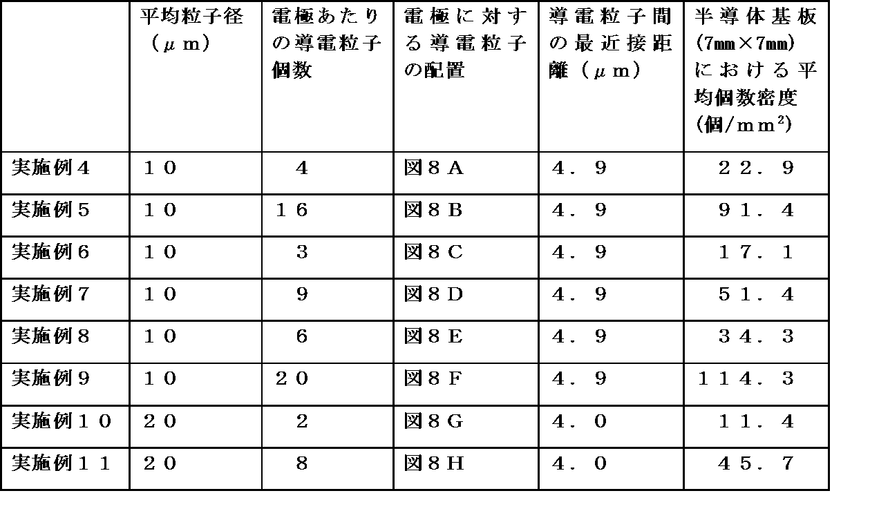
- Examples 4 to 11 In Examples 4 to 7, gold / nickel-coated resin particles (Micropearl, Sekisui Chemical Co., Ltd.) having an average particle diameter shown in Table 2 were used as the conductive particles in Example 1, and the conductive particles per electrode were used. The number, the arrangement of the conductive particles with respect to the electrodes, and the closest distance between the conductive particles are changed as shown in Table 2, and the conductive particles and the electrodes are directly aligned without forming an alignment mark by the arrangement of the conductive particles.
- the anisotropic conductive film was manufactured by repeating the operation of Example 1 except that the films were bonded together, the multilayer substrate using the anisotropic conductive film was manufactured, and the multilayer substrate was evaluated.
- each electrode 4 constituting the peripherally arranged electrodes (85 ⁇ m pitch, 280 pins) of the semiconductor substrate is changed from a circle of ⁇ 30 ⁇ m to a rectangle of 30 ⁇ m ⁇ 50 ⁇ m (electrode arrangement direction is 30 ⁇ m). And the same operation as in Examples 4 to 7 was repeated. As a result, in any of Examples 8 to 11, the conduction resistance, conduction reliability, and short-circuit occurrence rate were good.
- the conductive particles are nickel-coated resin particles having an average particle diameter of 10 ⁇ m (Micropearl, Sekisui Chemical Co., Ltd.), and the conductive particles are arranged in a tetragonal lattice (number of conductive particles) with a distance of 10 ⁇ m between the conductive particles.
- An anisotropic conductive film is manufactured by repeating the same operation as in Example 1 except that the density is 2500 pieces / mm 2 ), a multilayer substrate using the anisotropic conductive film is manufactured, and the multilayer substrate is evaluated. did. As a result, all the examples had good conduction resistance, conduction reliability, and short-circuit occurrence rate.
- the conductive particles are nickel-coated resin particles having an average particle diameter of 4 ⁇ m (Micropearl AUL704, Sekisui Chemical Co., Ltd.), and the conductive particles are arranged in a tetragonal lattice (with conductive particle distance of 4 ⁇ m).
- An anisotropic conductive film is manufactured by repeating the same operation as in Example 1 except that the number density is 16000 pieces / mm 2 ), a multilayer substrate using the anisotropic conductive film is manufactured, and the multilayer substrate is evaluated. As a result, all the examples had good conduction resistance, conduction reliability, and short-circuit occurrence rate.
Landscapes
- Non-Insulated Conductors (AREA)
- Wire Bonding (AREA)
- Engineering & Computer Science (AREA)
- Manufacturing & Machinery (AREA)
- Laminated Bodies (AREA)
- Production Of Multi-Layered Print Wiring Board (AREA)
- Cooling Or The Like Of Semiconductors Or Solid State Devices (AREA)
- Electric Connection Of Electric Components To Printed Circuits (AREA)
- Adhesive Tapes (AREA)
- Combinations Of Printed Boards (AREA)
Abstract
Description
多層基板の平面視において、貫通電極が対向する位置に導電粒子が選択的に存在し、
対向する貫通電極が導電粒子により接続され、該貫通電極が形成されている半導体基板同士が絶縁接着剤により接着している接続構造を有する多層基板を提供する。
第1半導体基板の貫通電極と第2半導体基板の貫通電極が対向し、それらの間に選択的に配置された導電粒子により接続され、
第1半導体基板と第2半導体基板が絶縁接着剤により接着している接続構造を有する態様を提供する。
該導電粒子ユニットにおいて、任意の導電粒子と、該導電粒子に最近接している導電粒子との距離が導電粒子径の0.2~0.5倍である異方導電性フィルムを提供する。
図1は、本発明の一実施態様の多層基板1Aの断面図である。
この多層基板1Aは、配線基板2に3層の半導体基板3A、3B、3Cが積層されたものであり、各半導体基板3A、3B、3Cは、IC等の半導体部品が形成された半導体ウエハである。配線基板2には貫通電極4Xが形成され、各半導体基板3A、3B、3Cには貫通電極4A、4B、4Cが形成されている。そして、配線基板2の表面で貫通電極4Xが露出する部分や、貫通電極4A、4B、4Cが半導体基板の表面に露出する部分には、それぞれ電極パッドが形成されている。なお、本発明において半導体基板3A、3B、3Cとしては、半導体チップを使用してもよい。また、本発明において、多層基板を構成する半導体基板の積層数に特に制限はない。
多層基板1Aは、後述するように多層基板を構成する各層を、導電粒子が特定の配置を有する本発明の異方導電性フィルムを用いて接続することにより製造される。異方導電性フィルムにおける導電粒子11の粒子径の大きさは、通常、貫通電極4A、4Bの対向面の径よりも小さいが、多層基板1Aでは、導電粒子11が当初の形状から潰れていることにより粒子径の大きさは、貫通電極4A、4Bの対向面の径と同程度となってもよい。これは、潰れた導電粒子11が貫通電極4A、4Bの対向面内に収まっていてもよく、外周部の少なくとも一部が、貫通電極4A、4Bの対向面からはみ出た状態でもよいことを意味する。なお、導電粒子11の構成素材にもよるが、導電粒子11は、多層基板1Aにおいても粒子形状を維持している場合がある。
ここで、多層基板1Aを構成する配線基板2としては、FR4等のガラスエポキシ基板等を使用することができる。配線基板2として、ICチップもしくはIC形成用のシリコンウェーハーを用いてもよい。配線基板2は、多層基板1Aの用途等に応じて適宜選択される。
配線基板2の電極部分には、必要に応じてハンダボール5が設けられる。
半導体基板3A、3B、3Cとしては、貫通電極4A、4B、4Cを有するものであれば特に制限は無く、例えば、シリコン等一般的半導体材料を使用することができる。
本発明の多層基板には、必要に応じて種々の部品を搭載することができる。
例えば図2に示す多層基板1Bは、各層の貫通電極4X、4A、4B、4Cが直線状に繋がった接続構造を有し、最外層には貫通電極4Cに接続した放熱用のヒートシンク6を有する。したがって、多層基板1Bは、配線基板2や半導体基板3A、3B、3Cに形成されたIC等の電子部品等から放出される熱をヒートシンク6により効率的に放熱することが可能となる。
本発明の多層基板の製造方法としては、例えば、図2の多層基板1Bの場合、まず、図3Aに示すように、貫通電極4Xを有する配線基板2と貫通電極4Aを有する半導体基板3Aとの間に、接続すべき貫通電極4X、4Aの配置に対応して導電粒子11が絶縁接着剤層12に選択的に配置された本発明の異方導電性フィルム10Aを挟み、異方導電性フィルム10Aを加熱加圧することにより配線基板2と第1半導体基板3Aを異方導電性接続し、図3Bに示す2層の接続構造体を得る。より具体的には、配線基板2と異方導電性フィルム10Aを、接続すべき貫通電極4Xと導電粒子11の配置が合うように位置合わせして重ね、さらに第1半導体基板3Aも同様に位置合わせして重ね合わせ、加熱加圧してこれらを異方導電性接続する。
本発明の多層基板の製造方法に使用する本発明の異方導電性フィルムは、接続すべき貫通電極の配置に対応して導電粒子11が絶縁接着剤層12に選択的に配置され、好ましくは導電粒子11によりアライメントマークが形成されたものである。アライメントマークとしては、導電粒子の配置により形成したものが好ましい。これにより、アライメントマークを明確に検出することができ、かつ異方導電性フィルムにアライメントマークをつけるための新たな工程の追加が不要となる。一方、アライメントマークは、レーザー照射などで絶縁接着剤層12を部分的に硬化させることにより形成してもよい。これによりアライメントマークを付する位置の変更が容易となる。
異方導電性フィルム10A、10Bを形成する導電粒子としては、公知の異方導電性フィルムに用いられているものの中から適宜選択することができる。例えば、ハンダ、ニッケル、コバルト、銀、銅、金、パラジウムなどの金属粒子、金属被覆樹脂粒子などが挙げられる。金属被覆樹脂粒子の金属被覆は、無電解メッキ法、スパッタリング法等の公知の金属膜形成方法を利用して形成することができる。金属被覆は、コア樹脂材の表面に形成されていれば特に制限はない。コア樹脂材は、樹脂のみから形成してもよく、導通信頼性の向上のために導電微粒子を含有させたものとしてもよい。
絶縁接着剤層12としては、公知の異方導電性フィルムで使用される絶縁性樹脂層を適宜採用することができる。例えば、アクリレート化合物と光ラジカル重合開始剤とを含む光ラジカル重合型樹脂層、アクリレート化合物と熱ラジカル重合開始剤とを含む熱ラジカル重合型樹脂層、エポキシ化合物と熱カチオン重合開始剤とを含む熱カチオン重合型樹脂層、エポキシ化合物と熱アニオン重合開始剤とを含む熱アニオン重合型樹脂層等を使用することができる。また、これらの樹脂層は、必要に応じて、それぞれ重合したものとすることができる。また、絶縁接着剤層12を、複数の樹脂層から形成してもよい。
絶縁性フィラーの大きさは、異方導電性接続を阻害しない大きさであることが望ましい。
本発明の多層基板は種々の態様をとることができる。
例えば、図4に示す多層基板1Cは、図1に示した多層基板1Aにおいて、配線基板2の貫通電極4Xと第1半導体基板3Aの貫通電極4Aとを接続する異方導電性フィルムと、第1半導体基板3Aの貫通電極4Aと第2半導体基板3Bの貫通電極4Bとを接続する異方導電性フィルムと、第2半導体基板3Bの貫通電極4Bと第3半導体基板3Cの貫通電極4Cとを接続する異方導電性フィルムとして、共通する異方導電性フィルムを使用することにより製造したものである。即ち、異方導電性フィルムとして、製造しようとする多層基板1Cの平面視において、配線基板2又は各半導体基板3A、3B、3Cの貫通電極同士が対向する位置に対応して導電粒子11が絶縁接着剤層12に選択的に配置されたものが使用される。これにより、多層基板1Cの平面視において、貫通電極4X、4A、4B、4Cが対向する位置に導電粒子11、11xが存在することになる。言い換えると、対向する貫通電極の間には、必ずしも該貫通電極のみに対して選択的に配置された導電粒子が存在するわけではない。例えば、半導体基板3Aと半導体基板3Bとの間には、これらに形成されている貫通電極4A、4Bが対向する位置に導電粒子11が選択的に配置されている他、半導体基板3Aの貫通電極4Aと半導体基板の貫通電極4Bとの接続には寄与しない導電粒子11xも存在する。よって、半導体基板3Aと半導体基板3Bとの間に存在する全導電粒子に対し、半導体基板3Aと半導体基板3Bとの間で貫通電極に捕捉されない導電粒子が5%を超えて存在し得る。しかし、半導体基板3Aと半導体基板3Bの間にあってこれらの接続に寄与していない導電粒子11xは、配線基板2の貫通電極4Xと第1半導体基板3Aの貫通電極4Aとの接続に寄与している。また、多層基板1Cの平面視において、貫通電極同士が対向しない位置には、導電粒子は配置されていない、あるいは実質的に存在していない。即ち、図4に示す多層基板1Cにおいて、多層基板のフィルム厚方向の任意の断面の各半導体基板間には、全ての貫通電極と垂直方向に重なる位置に導電粒子が存在している状態が好ましい。
図5Aに示す多層基板1Dは、図1に示した多層基板1Aにおいて、対向する貫通電極4X、4A、4B、4Cが、それぞれ2個以上の導電粒子11により接続されているものである。図5Bは、この接続に使用する異方導電性フィルム10Dにおける導電粒子11の配置を示す平面図である。
各半導体基板を、共通する異方導電性フィルムを用いて接続することにより多層基板の製造に要するトータルコストを削減する場合に、導電粒子ユニット11uが一面に配置されている異方導電性フィルムを使用して多層基板を製造してもよい。この場合、各導電粒子ユニット11uを構成する導電粒子数は3個以上、好ましくは12個以上、より好ましくは20個以上であり、各導電粒子ユニット内で導電粒子が一列ではなく、面状に配置されているものとする。導電粒子ユニット11u同士の間隔は、ショートの発生を回避するため、導電粒子径の1倍以上とし、半導体基板の電極間隔に応じて適宜定める。導電粒子ユニットの径もしくは最長辺の長さの、電極の径もしくは最長辺の長さに対する割合は、小さすぎると電極における導電粒子の捕捉性が劣り、大きすぎるとショートの発生が懸念されることから、下限が好ましくは0.3倍以上、より好ましくは0.5倍以上、さらに好ましくは0.7倍以上であり、上限が好ましくは3倍以下、より好ましくは2倍以下である。また、導電粒子ユニットの径もしくは最長辺の長さが、電極の径もしくは最長辺の長さの等倍未満であれば電極内に導電粒子ユニットが収まることになるため、導電粒子の挟待の状態は良好になり易く、等倍以上であれば導電粒子と電極の位置あわせにおけるマージンが広くなるので多層基板の製造時間の短縮を図ることができる。
実施例1~3、比較例1
(1)半導体基板
多層基板を構成する半導体基板3として、外形が7mm□、厚み200μmの矩形で、図6に示すように、クロム製電極パッドを有する貫通電極4がペリフェラル配置(φ30μm、85μmピッチ、280ピン)に形成されているものを用意した。半導体基板には、アライメントマークとして200μm□の四角形マークが形成されている。
表1に示すように、所定の粒子径の導電粒子(微粉半田粉、三井金属鉱業(株))を、絶縁接着剤層にランダムに配置するか(比較例1、粒子密度17.1個/mm2)、又は半導体基板の電極配置に対応させて配置した(実施例1~3、85μmピッチ、280箇所)異方導電性フィルムを製造した。
(1)で用意した半導体基板を、(2)で製造した異方導電性フィルムを用いて表1に示した積層数で重ね合わせ、加熱加圧(180℃、40MPa、20秒)することにより多層基板を製造した。
得られた多層基板について、(a)導通抵抗、(b)導通信頼性、(c)ショート発生
率、を次のように評価した。これらの結果を表1に示す。
多層基板の表裏の電極間の導通抵抗を、デジタルマルチメータ(34401A、アジレント・テクノロジー(株))を使用し、4端子法にて、電流1mAを流して測定した。測定された抵抗値が5Ω以下をOKとし、5Ωを超えるものをNGとした。
多層基板を温度85℃、湿度85%RHの恒温槽に500時間おいた後の導通抵抗を、(a)と同様に測定し、その導通抵抗が10Ω以下をOKとし、10Ωを超えるものをNGとした。
積層した半導体基板を一枚ずつ剥離し、隣り合う電極が導電粒子でショートしているか否かを観察し、ショートが無い場合をOK、1つでもあるとNGとした。

実施例4~7では、実施例1において、導電粒子として表2に示す平均粒子径の金/ニッケル被覆樹脂粒子(ミクロパール、積水化学工業(株))を使用し、電極あたりの導電粒子の個数と、電極に対する導電粒子の配置と、導電粒子間の最近接距離を表2に示すように変更し、導電粒子の配列によりアライメントマークを形成することなく導電粒子と電極とを直接位置合わせしてフィルムを貼り合わせた以外は、実施例1の操作を繰り返すことにより異方導電性フィルムを製造し、異方導電性フィルムを用いた多層基板を製造し、多層基板を評価した。その結果、実施例4~7のいずれにおいても導通抵抗、導通信頼性、及びショート発生率が良好であった。なお、実施例5、7、9では、アライメントマークに対応する導電粒子の配列がなくても、電極の外周部にも導電粒子を存在させたため、フィルムの貼り合せ工程で位置ずれの許容範囲を広くすることができた。
実施例1において、導電粒子を平均粒子径10μmのニッケル被覆樹脂粒子(ミクロパール、積水化学工業(株))とし、導電粒子の配置を、導電粒子間距離10μmの4方格子(導電粒子の個数密度:2500個/mm2)とする以外は実施例1と同様の操作を繰り返すことにより異方導電性フィルムを製造し、異方導電性フィルムを用いた多層基板を製造し、多層基板を評価した。その結果、いずれの実施例も導通抵抗、導通信頼性、及びショート発生率が良好であった。
実施例1において、導電粒子を平均粒子径4μmのニッケル被覆樹脂粒子(ミクロパールAUL704、積水化学工業(株))とし、導電粒子の配置を、導電粒子間距離4μmの4方格子(導電粒子の個数密度:16000個/mm2)とする以外は実施例1と同様の操作を繰り返すことにより異方導電性フィルムを製造し、異方導電性フィルムを用いた多層基板を製造し、多層基板を評価した。その結果、いずれの実施例も導通抵抗、導通信頼性、及びショート発生率が良好であった。
2 配線基板
3、3A、3B、3C 半導体基板
4、4A、4B、4C、4x 貫通電極
5 ハンダボール
6 ヒートシンク
10A、10B、10D 異方導電性フィルム
11、11x 導電粒子
11u 導電粒子ユニット
12 絶縁接着剤又は絶縁接着剤層
L 導電粒子間の距離
Claims (12)
- 貫通電極を有する半導体基板が積層されている多層基板であって、
多層基板の平面視において、貫通電極が対向する位置に導電粒子が選択的に存在し、
対向する貫通電極が導電粒子により接続され、該貫通電極が形成されている半導体基板同士が絶縁接着剤により接着している接続構造を有する多層基板。 - 貫通電極を有する第1半導体基板と、貫通電極を有する第2半導体基板とが積層されている多層基板であって、
第1半導体基板の貫通電極と第2半導体基板の貫通電極が、それらの間に選択的に配置された導電粒子により接続されている接続構造を有する請求項1記載の多層基板。 - 貫通電極を有する第3半導体基板が第2半導体基板に積層されており、
第1半導体基板の貫通電極と接続している第2半導体基板の貫通電極と第3半導体基板の貫通電極とが対向し、それらの間に選択的に配置された導電粒子により接続され、
第2半導体基板と第3半導体基板が絶縁接着剤により接着している接続構造を有する請求項2記載の多層基板。 - 第1半導体基板と第2半導体基板の間で、対向する貫通電極に捕捉されていない導電粒子の数が第1半導体基板と第2半導体基板の間に存在する導電粒子の総数の5%以下である請求項1~3のいずれかに記載の多層基板。
- 多層基板の最外層にヒートシンクを有し、ヒートシンクと、導電粒子で接続されることにより多層基板の積層方向に繋がった貫通電極とが接続している請求項1~4のいずれかに記載の多層基板。
- 半導体基板に形成された貫通電極同士を対向させて接合する多層基板の製造方法であって、貫通電極が対向する部分の多層基板の平面視における位置に対応して導電粒子が絶縁接着剤層に選択的に配置された異方導電性フィルムを、貫通電極を有する半導体基板同士の間に挟み、該異方導電性フィルムを加熱加圧することによりこれら半導体基板を異方導電性接続する多層基板の製造方法。
- 貫通電極を有する第1半導体基板と、貫通電極を有する第2半導体基板を、それらの貫通電極同士を対向させて接合する多層基板の製造方法であって、第1半導体基板と第2半導体基板との間に、貫通電極の配置に対応して導電粒子が絶縁接着剤層に選択的に配置された異方導電性フィルムを挟み、該異方導電性フィルムを加熱加圧することにより第1半導体基板と第2半導体基板を異方導電性接続する請求項6記載の多層基板の製造方法。
- 貫通電極を有する第3半導体基板を第2半導体基板に積層し、第1半導体基板の貫通電極と異方導電性接続した第2半導体基板の貫通電極と、第3半導体基板の貫通電極との間に、貫通電極の配置に対応して導電粒子が絶縁接着剤層に選択的に配置された異方導電性フィルムを挟み、該異方導電性フィルムを加熱加圧することにより第2半導体基板と第3半導体基板を異方導電性接続する請求項6又は7記載の多層基板の製造方法。
- 絶縁接着剤層と、該絶縁接着剤層に配置された導電粒子を含む異方導電性フィルムであって、異方導電性フィルムで接続する貫通電極の配置に対応して導電粒子が絶縁接着剤層に選択的に配置されている異方導電性フィルム。
- 絶縁接着剤層と、該絶縁接着剤層に配置された導電粒子を含む異方導電性フィルムであって、3個以上の導電粒子が近接している導電粒子ユニットが形成されており、
該導電粒子ユニットにおいて、任意の導電粒子と、該導電粒子に最近接している導電粒子との距離が導電粒子径の0.2~0.5倍である異方導電性フィルム。 - 導電粒子ユニットが、異方導電性フィルムで接続する貫通電極の配置に対応して配置されている請求項10記載の異方導電性フィルム。
- 導電粒子が、金属被覆樹脂粒子である請求項9~11のいずれかに記載の異方導電性フィルム。
Priority Applications (4)
| Application Number | Priority Date | Filing Date | Title |
|---|---|---|---|
| KR1020177017940A KR101974763B1 (ko) | 2015-01-13 | 2016-01-13 | 다층 기판 |
| CN201680004447.3A CN107112314B (zh) | 2015-01-13 | 2016-01-13 | 多层基板 |
| CN202110755784.9A CN113690209B (zh) | 2015-01-13 | 2016-01-13 | 多层基板 |
| US15/543,397 US10199358B2 (en) | 2015-01-13 | 2016-01-13 | Multilayer substrate |
Applications Claiming Priority (2)
| Application Number | Priority Date | Filing Date | Title |
|---|---|---|---|
| JP2015-004595 | 2015-01-13 | ||
| JP2015004595 | 2015-01-13 |
Publications (1)
| Publication Number | Publication Date |
|---|---|
| WO2016114318A1 true WO2016114318A1 (ja) | 2016-07-21 |
Family
ID=56405859
Family Applications (1)
| Application Number | Title | Priority Date | Filing Date |
|---|---|---|---|
| PCT/JP2016/050873 Ceased WO2016114318A1 (ja) | 2015-01-13 | 2016-01-13 | 多層基板 |
Country Status (6)
| Country | Link |
|---|---|
| US (1) | US10199358B2 (ja) |
| JP (2) | JP2016131245A (ja) |
| KR (1) | KR101974763B1 (ja) |
| CN (2) | CN107112314B (ja) |
| TW (3) | TWI709221B (ja) |
| WO (1) | WO2016114318A1 (ja) |
Cited By (1)
| Publication number | Priority date | Publication date | Assignee | Title |
|---|---|---|---|---|
| WO2019078291A1 (ja) * | 2017-10-20 | 2019-04-25 | ソニーセミコンダクタソリューションズ株式会社 | 撮像装置 |
Families Citing this family (9)
| Publication number | Priority date | Publication date | Assignee | Title |
|---|---|---|---|---|
| CN114221146B (zh) | 2016-11-30 | 2024-11-22 | 迪睿合株式会社 | 导电粒子配置膜、其制造方法、检查探头单元、导通检查方法 |
| JP7042037B2 (ja) * | 2017-04-24 | 2022-03-25 | デクセリアルズ株式会社 | 検査冶具の製造方法 |
| JP7046351B2 (ja) | 2018-01-31 | 2022-04-04 | 三国電子有限会社 | 接続構造体の作製方法 |
| JP7185252B2 (ja) | 2018-01-31 | 2022-12-07 | 三国電子有限会社 | 接続構造体の作製方法 |
| JP7160302B2 (ja) * | 2018-01-31 | 2022-10-25 | 三国電子有限会社 | 接続構造体および接続構造体の作製方法 |
| CN112543693A (zh) | 2018-06-26 | 2021-03-23 | 昭和电工材料株式会社 | 焊料粒子 |
| WO2020004510A1 (ja) * | 2018-06-26 | 2020-01-02 | 日立化成株式会社 | 異方性導電フィルム及びその製造方法並びに接続構造体の製造方法 |
| JP7125547B2 (ja) * | 2018-12-29 | 2022-08-24 | 深南電路股▲ふん▼有限公司 | 多様に組み立て可能なプリント基板及びその製造方法 |
| KR102928946B1 (ko) * | 2021-02-05 | 2026-02-20 | 엘지이노텍 주식회사 | 회로기판 및 이를 포함하는 패키지 기판 |
Citations (6)
| Publication number | Priority date | Publication date | Assignee | Title |
|---|---|---|---|---|
| JPH0362411A (ja) * | 1989-07-31 | 1991-03-18 | Canon Inc | 異方性導電フィルムの製造方法 |
| JP2001237365A (ja) * | 2000-02-23 | 2001-08-31 | Seiko Epson Corp | 接続用端子の接合方法、半導体装置の製造方法および半導体装置 |
| JP2002110897A (ja) * | 2000-09-28 | 2002-04-12 | Toshiba Corp | 半導体装置およびその製造方法 |
| WO2003003798A1 (fr) * | 2001-06-29 | 2003-01-09 | Toray Engineering Co., Ltd. | Methode d'assemblage utilisant un adhesif conducteur anisotrope |
| JP2006245311A (ja) * | 2005-03-03 | 2006-09-14 | Oki Electric Ind Co Ltd | 半導体装置及びその製造方法 |
| JP2006310082A (ja) * | 2005-04-28 | 2006-11-09 | Tokai Rubber Ind Ltd | 異方性導電膜およびその製造方法 |
Family Cites Families (56)
| Publication number | Priority date | Publication date | Assignee | Title |
|---|---|---|---|---|
| JPS6234773A (ja) | 1985-08-02 | 1987-02-14 | Honda Motor Co Ltd | 研削盤における砥石ストツク装置 |
| JPH0334064Y2 (ja) * | 1985-08-21 | 1991-07-18 | ||
| US5502889A (en) * | 1988-06-10 | 1996-04-02 | Sheldahl, Inc. | Method for electrically and mechanically connecting at least two conductive layers |
| JP2748713B2 (ja) * | 1991-03-29 | 1998-05-13 | 日立化成工業株式会社 | 接続部材 |
| JPH08330736A (ja) | 1995-06-01 | 1996-12-13 | Toray Ind Inc | 多層基板およびその製造方法 |
| JPH1056099A (ja) * | 1996-08-12 | 1998-02-24 | Shinko Electric Ind Co Ltd | 多層回路基板およびその製造方法 |
| US5965064A (en) * | 1997-10-28 | 1999-10-12 | Sony Chemicals Corporation | Anisotropically electroconductive adhesive and adhesive film |
| JP3624818B2 (ja) * | 1999-10-12 | 2005-03-02 | ソニーケミカル株式会社 | 異方性導電接続材料、接続体、およびその製造方法 |
| JP2003204135A (ja) * | 2002-09-20 | 2003-07-18 | Canon Inc | マルチチップモジュール、及びディスプレイパネル |
| JP3740469B2 (ja) * | 2003-01-31 | 2006-02-01 | 株式会社東芝 | 半導体装置および半導体装置の製造方法 |
| JP4340517B2 (ja) | 2003-10-30 | 2009-10-07 | Okiセミコンダクタ株式会社 | 半導体装置及びその製造方法 |
| JP4351939B2 (ja) * | 2004-03-25 | 2009-10-28 | ソニーケミカル&インフォメーションデバイス株式会社 | 多層配線基板及びその製造方法 |
| JP5123664B2 (ja) * | 2005-09-28 | 2013-01-23 | スパンション エルエルシー | 半導体装置およびその製造方法 |
| WO2007043639A1 (ja) * | 2005-10-14 | 2007-04-19 | Fujikura Ltd. | プリント配線基板及びプリント配線基板の製造方法 |
| JP4827851B2 (ja) * | 2005-11-22 | 2011-11-30 | ソニー株式会社 | 半導体装置および半導体装置の製造方法 |
| KR100777255B1 (ko) | 2006-04-18 | 2007-11-20 | 중앙대학교 산학협력단 | 이방성 도전 필름 및 이를 이용한 전자부품의 실장방법 |
| JP2006339160A (ja) | 2006-06-02 | 2006-12-14 | Hitachi Chem Co Ltd | 熱硬化性回路接続部材及びそれを用いた電極の接続構造、電極の接続方法 |
| WO2008058039A1 (en) * | 2006-11-06 | 2008-05-15 | University Of Florida Research Foundation, Inc. | Devices and methods for utilizing mechanical surgical devices in a virtual environment |
| JP4872663B2 (ja) * | 2006-12-28 | 2012-02-08 | 株式会社日立製作所 | 接合用材料及び接合方法 |
| KR100842921B1 (ko) * | 2007-06-18 | 2008-07-02 | 주식회사 하이닉스반도체 | 반도체 패키지의 제조 방법 |
| KR20090011568A (ko) * | 2007-07-26 | 2009-02-02 | 주식회사 하이닉스반도체 | 반도체 패키지 및 그의 제조 방법 |
| JP5291917B2 (ja) * | 2007-11-09 | 2013-09-18 | ルネサスエレクトロニクス株式会社 | 半導体装置およびその製造方法 |
| WO2009119904A1 (ja) * | 2008-03-28 | 2009-10-01 | 日本電気株式会社 | 半導体装置、その製造方法、プリント回路基板および電子機器 |
| US8334170B2 (en) * | 2008-06-27 | 2012-12-18 | Taiwan Semiconductor Manufacturing Company, Ltd. | Method for stacking devices |
| US8097953B2 (en) * | 2008-10-28 | 2012-01-17 | Taiwan Semiconductor Manufacturing Company, Ltd. | Three-dimensional integrated circuit stacking-joint interface structure |
| US8674482B2 (en) * | 2008-11-18 | 2014-03-18 | Hong Kong Applied Science And Technology Research Institute Co. Ltd. | Semiconductor chip with through-silicon-via and sidewall pad |
| JP4730426B2 (ja) * | 2008-11-19 | 2011-07-20 | ソニー株式会社 | 実装基板及び半導体モジュール |
| KR20100079183A (ko) * | 2008-12-30 | 2010-07-08 | 주식회사 동부하이텍 | 반도체 패키지 장치와 그 제조 방법 |
| US8647923B2 (en) * | 2009-04-06 | 2014-02-11 | Canon Kabushiki Kaisha | Method of manufacturing semiconductor device |
| JP2010251547A (ja) * | 2009-04-16 | 2010-11-04 | Elpida Memory Inc | 半導体装置及びその製造方法 |
| JP2010272737A (ja) | 2009-05-22 | 2010-12-02 | Elpida Memory Inc | 半導体装置の製造方法 |
| JP4825286B2 (ja) * | 2009-08-07 | 2011-11-30 | ナミックス株式会社 | 多層配線板の製造方法 |
| JP5595708B2 (ja) * | 2009-10-09 | 2014-09-24 | ピーエスフォー ルクスコ エスエイアールエル | 半導体装置及びその調整方法並びにデータ処理システム |
| JP5271886B2 (ja) * | 2009-12-08 | 2013-08-21 | ルネサスエレクトロニクス株式会社 | 半導体装置およびその製造方法 |
| US8232137B2 (en) * | 2009-12-10 | 2012-07-31 | Intersil Americas Inc. | Heat conduction for chip stacks and 3-D circuits |
| US8048721B2 (en) * | 2010-03-18 | 2011-11-01 | Powertech Technology Inc. | Method for filling multi-layer chip-stacked gaps |
| JP2011222553A (ja) * | 2010-04-02 | 2011-11-04 | Denso Corp | 半導体チップ内蔵配線基板及びその製造方法 |
| JP2011243725A (ja) * | 2010-05-18 | 2011-12-01 | Elpida Memory Inc | 半導体装置の製造方法 |
| KR20130133748A (ko) * | 2010-06-17 | 2013-12-09 | 모사이드 테크놀로지스 인코퍼레이티드 | 관통 실리콘 비아를 갖는 반도체 디바이스 |
| US8445918B2 (en) * | 2010-08-13 | 2013-05-21 | International Business Machines Corporation | Thermal enhancement for multi-layer semiconductor stacks |
| KR20120032254A (ko) * | 2010-09-28 | 2012-04-05 | 삼성전자주식회사 | 반도체 적층 패키지 및 이의 제조 방법 |
| KR101421907B1 (ko) * | 2010-12-01 | 2014-07-22 | 파나소닉 주식회사 | 전자 부품 실장체, 전자 부품 및 기판 |
| JP5167335B2 (ja) * | 2010-12-22 | 2013-03-21 | 株式会社日立製作所 | 半導体装置 |
| KR101817156B1 (ko) * | 2010-12-28 | 2018-01-10 | 삼성전자 주식회사 | 관통 전극을 갖는 적층 구조의 반도체 장치, 반도체 메모리 장치, 반도체 메모리 시스템 및 그 동작방법 |
| JP5932267B2 (ja) * | 2011-08-31 | 2016-06-08 | ピーエスフォー ルクスコ エスエイアールエルPS4 Luxco S.a.r.l. | 半導体装置及びその製造方法 |
| JP5780228B2 (ja) * | 2011-11-11 | 2015-09-16 | 住友ベークライト株式会社 | 半導体装置の製造方法 |
| KR101784507B1 (ko) * | 2011-12-14 | 2017-10-12 | 에스케이하이닉스 주식회사 | 반도체 적층 패키지 및 제조 방법, 이를 포함하는 전자 시스템 |
| WO2013089199A1 (ja) * | 2011-12-16 | 2013-06-20 | 旭化成イーマテリアルズ株式会社 | 異方導電性フィルム付き半導体チップ、異方導電性フィルム付き半導体ウェハ、及び半導体装置 |
| JP2013183120A (ja) * | 2012-03-05 | 2013-09-12 | Elpida Memory Inc | 半導体装置 |
| CN104541417B (zh) * | 2012-08-29 | 2017-09-26 | 迪睿合电子材料有限公司 | 各向异性导电膜及其制备方法 |
| JP6058336B2 (ja) * | 2012-09-28 | 2017-01-11 | ルネサスエレクトロニクス株式会社 | 半導体装置 |
| KR20140099604A (ko) * | 2013-02-04 | 2014-08-13 | 삼성전자주식회사 | 적층 패키지 및 적층 패키지의 제조 방법 |
| KR20150005113A (ko) * | 2013-07-04 | 2015-01-14 | 에스케이하이닉스 주식회사 | 광학 신호 경로를 포함하는 반도체 패키지 |
| KR102084540B1 (ko) * | 2013-10-16 | 2020-03-04 | 삼성전자주식회사 | 반도체 패키지 및 그 제조방법 |
| JP2015177062A (ja) * | 2014-03-14 | 2015-10-05 | 株式会社東芝 | 半導体装置の製造方法および半導体装置 |
| US9349670B2 (en) * | 2014-08-04 | 2016-05-24 | Micron Technology, Inc. | Semiconductor die assemblies with heat sink and associated systems and methods |
-
2016
- 2016-01-13 TW TW105101041A patent/TWI709221B/zh active
- 2016-01-13 US US15/543,397 patent/US10199358B2/en active Active
- 2016-01-13 TW TW111142394A patent/TWI838943B/zh active
- 2016-01-13 KR KR1020177017940A patent/KR101974763B1/ko active Active
- 2016-01-13 JP JP2016004538A patent/JP2016131245A/ja active Pending
- 2016-01-13 TW TW109134185A patent/TWI786440B/zh active
- 2016-01-13 CN CN201680004447.3A patent/CN107112314B/zh active Active
- 2016-01-13 WO PCT/JP2016/050873 patent/WO2016114318A1/ja not_active Ceased
- 2016-01-13 CN CN202110755784.9A patent/CN113690209B/zh active Active
-
2020
- 2020-09-25 JP JP2020161099A patent/JP7207382B2/ja active Active
Patent Citations (6)
| Publication number | Priority date | Publication date | Assignee | Title |
|---|---|---|---|---|
| JPH0362411A (ja) * | 1989-07-31 | 1991-03-18 | Canon Inc | 異方性導電フィルムの製造方法 |
| JP2001237365A (ja) * | 2000-02-23 | 2001-08-31 | Seiko Epson Corp | 接続用端子の接合方法、半導体装置の製造方法および半導体装置 |
| JP2002110897A (ja) * | 2000-09-28 | 2002-04-12 | Toshiba Corp | 半導体装置およびその製造方法 |
| WO2003003798A1 (fr) * | 2001-06-29 | 2003-01-09 | Toray Engineering Co., Ltd. | Methode d'assemblage utilisant un adhesif conducteur anisotrope |
| JP2006245311A (ja) * | 2005-03-03 | 2006-09-14 | Oki Electric Ind Co Ltd | 半導体装置及びその製造方法 |
| JP2006310082A (ja) * | 2005-04-28 | 2006-11-09 | Tokai Rubber Ind Ltd | 異方性導電膜およびその製造方法 |
Cited By (3)
| Publication number | Priority date | Publication date | Assignee | Title |
|---|---|---|---|---|
| WO2019078291A1 (ja) * | 2017-10-20 | 2019-04-25 | ソニーセミコンダクタソリューションズ株式会社 | 撮像装置 |
| JPWO2019078291A1 (ja) * | 2017-10-20 | 2020-11-26 | ソニーセミコンダクタソリューションズ株式会社 | 撮像装置 |
| US11456323B2 (en) | 2017-10-20 | 2022-09-27 | Sony Semiconductor Solutions Corporation | Imaging unit |
Also Published As
| Publication number | Publication date |
|---|---|
| JP2020202409A (ja) | 2020-12-17 |
| KR20170093171A (ko) | 2017-08-14 |
| CN107112314A (zh) | 2017-08-29 |
| CN113690209A (zh) | 2021-11-23 |
| TW202312423A (zh) | 2023-03-16 |
| TWI838943B (zh) | 2024-04-11 |
| CN113690209B (zh) | 2025-07-25 |
| TW202107672A (zh) | 2021-02-16 |
| TWI786440B (zh) | 2022-12-11 |
| TW201639115A (zh) | 2016-11-01 |
| US10199358B2 (en) | 2019-02-05 |
| CN107112314B (zh) | 2021-07-27 |
| JP2016131245A (ja) | 2016-07-21 |
| US20180026012A1 (en) | 2018-01-25 |
| TWI709221B (zh) | 2020-11-01 |
| JP7207382B2 (ja) | 2023-01-18 |
| KR101974763B1 (ko) | 2019-05-02 |
Similar Documents
| Publication | Publication Date | Title |
|---|---|---|
| JP7207382B2 (ja) | 多層基板 | |
| JP6504307B1 (ja) | 異方導電性フィルム | |
| CN106797082B (zh) | 各向异性导电膜及连接结构体 | |
| JP7207383B2 (ja) | 多層基板 | |
| TWI686014B (zh) | 異向導電性膜、連接結構體、及連接結構體之製造方法 | |
| KR101999913B1 (ko) | 이방 도전성 필름 및 접속 구조체 | |
| KR102688696B1 (ko) | 전자 부품, 이방성 접속 구조체, 전자 부품의 설계 방법 | |
| JP2017175093A (ja) | 電子部品、接続体、電子部品の設計方法 | |
| WO2008050521A1 (en) | 3d electronic circuit device | |
| HK40064907A (en) | Multilayer board | |
| HK1240400A1 (en) | Multilayer board | |
| HK1240400B (zh) | 多层基板 | |
| HK1242473A1 (en) | Multilayer substrate | |
| JP2023117329A (ja) | 導電フィルムの設計方法 | |
| HK1242473B (zh) | 多层基板 |
Legal Events
| Date | Code | Title | Description |
|---|---|---|---|
| 121 | Ep: the epo has been informed by wipo that ep was designated in this application |
Ref document number: 16737389 Country of ref document: EP Kind code of ref document: A1 |
|
| DPE1 | Request for preliminary examination filed after expiration of 19th month from priority date (pct application filed from 20040101) | ||
| ENP | Entry into the national phase |
Ref document number: 20177017940 Country of ref document: KR Kind code of ref document: A |
|
| WWE | Wipo information: entry into national phase |
Ref document number: 15543397 Country of ref document: US |
|
| NENP | Non-entry into the national phase |
Ref country code: DE |
|
| 122 | Ep: pct application non-entry in european phase |
Ref document number: 16737389 Country of ref document: EP Kind code of ref document: A1 |