WO2012165124A1 - 酸化モリブデンを含有する薄膜の製造方法、酸化モリブデンを含有する薄膜の形成用原料及びモリブデンアミド化合物 - Google Patents
酸化モリブデンを含有する薄膜の製造方法、酸化モリブデンを含有する薄膜の形成用原料及びモリブデンアミド化合物 Download PDFInfo
- Publication number
- WO2012165124A1 WO2012165124A1 PCT/JP2012/062199 JP2012062199W WO2012165124A1 WO 2012165124 A1 WO2012165124 A1 WO 2012165124A1 JP 2012062199 W JP2012062199 W JP 2012062199W WO 2012165124 A1 WO2012165124 A1 WO 2012165124A1
- Authority
- WO
- WIPO (PCT)
- Prior art keywords
- thin film
- molybdenum
- molybdenum oxide
- compound
- amide compound
- Prior art date
- Legal status (The legal status is an assumption and is not a legal conclusion. Google has not performed a legal analysis and makes no representation as to the accuracy of the status listed.)
- Ceased
Links
Images


Classifications
-
- C—CHEMISTRY; METALLURGY
- C23—COATING METALLIC MATERIAL; COATING MATERIAL WITH METALLIC MATERIAL; CHEMICAL SURFACE TREATMENT; DIFFUSION TREATMENT OF METALLIC MATERIAL; COATING BY VACUUM EVAPORATION, BY SPUTTERING, BY ION IMPLANTATION OR BY CHEMICAL VAPOUR DEPOSITION, IN GENERAL; INHIBITING CORROSION OF METALLIC MATERIAL OR INCRUSTATION IN GENERAL
- C23C—COATING METALLIC MATERIAL; COATING MATERIAL WITH METALLIC MATERIAL; SURFACE TREATMENT OF METALLIC MATERIAL BY DIFFUSION INTO THE SURFACE, BY CHEMICAL CONVERSION OR SUBSTITUTION; COATING BY VACUUM EVAPORATION, BY SPUTTERING, BY ION IMPLANTATION OR BY CHEMICAL VAPOUR DEPOSITION, IN GENERAL
- C23C16/00—Chemical coating by decomposition of gaseous compounds, without leaving reaction products of surface material in the coating, i.e. chemical vapour deposition [CVD] processes
- C23C16/22—Chemical coating by decomposition of gaseous compounds, without leaving reaction products of surface material in the coating, i.e. chemical vapour deposition [CVD] processes characterised by the deposition of inorganic material, other than metallic material
- C23C16/30—Deposition of compounds, mixtures or solid solutions, e.g. borides, carbides, nitrides
- C23C16/40—Oxides
-
- H—ELECTRICITY
- H10—SEMICONDUCTOR DEVICES; ELECTRIC SOLID-STATE DEVICES NOT OTHERWISE PROVIDED FOR
- H10D—INORGANIC ELECTRIC SEMICONDUCTOR DEVICES
- H10D64/00—Electrodes of devices having potential barriers
- H10D64/01—Manufacture or treatment
- H10D64/013—Manufacture or treatment of electrodes having a conductor capacitively coupled to a semiconductor by an insulator
- H10D64/01302—Manufacture or treatment of electrodes having a conductor capacitively coupled to a semiconductor by an insulator the insulator being formed after the semiconductor body, the semiconductor being silicon
- H10D64/01332—Making the insulator
- H10D64/01336—Making the insulator on single crystalline silicon, e.g. chemical oxidation using a liquid
- H10D64/01342—Making the insulator on single crystalline silicon, e.g. chemical oxidation using a liquid by deposition, e.g. evaporation, ALD or laser deposition
-
- C—CHEMISTRY; METALLURGY
- C07—ORGANIC CHEMISTRY
- C07C—ACYCLIC OR CARBOCYCLIC COMPOUNDS
- C07C211/00—Compounds containing amino groups bound to a carbon skeleton
- C07C211/01—Compounds containing amino groups bound to a carbon skeleton having amino groups bound to acyclic carbon atoms
- C07C211/02—Compounds containing amino groups bound to a carbon skeleton having amino groups bound to acyclic carbon atoms of an acyclic saturated carbon skeleton
- C07C211/03—Monoamines
-
- C—CHEMISTRY; METALLURGY
- C07—ORGANIC CHEMISTRY
- C07F—ACYCLIC, CARBOCYCLIC OR HETEROCYCLIC COMPOUNDS CONTAINING ELEMENTS OTHER THAN CARBON, HYDROGEN, HALOGEN, OXYGEN, NITROGEN, SULFUR, SELENIUM OR TELLURIUM
- C07F11/00—Compounds containing elements of Groups 6 or 16 of the Periodic Table
-
- C—CHEMISTRY; METALLURGY
- C07—ORGANIC CHEMISTRY
- C07F—ACYCLIC, CARBOCYCLIC OR HETEROCYCLIC COMPOUNDS CONTAINING ELEMENTS OTHER THAN CARBON, HYDROGEN, HALOGEN, OXYGEN, NITROGEN, SULFUR, SELENIUM OR TELLURIUM
- C07F11/00—Compounds containing elements of Groups 6 or 16 of the Periodic Table
- C07F11/005—Compounds containing elements of Groups 6 or 16 of the Periodic Table compounds without a metal-carbon linkage
-
- C—CHEMISTRY; METALLURGY
- C23—COATING METALLIC MATERIAL; COATING MATERIAL WITH METALLIC MATERIAL; CHEMICAL SURFACE TREATMENT; DIFFUSION TREATMENT OF METALLIC MATERIAL; COATING BY VACUUM EVAPORATION, BY SPUTTERING, BY ION IMPLANTATION OR BY CHEMICAL VAPOUR DEPOSITION, IN GENERAL; INHIBITING CORROSION OF METALLIC MATERIAL OR INCRUSTATION IN GENERAL
- C23C—COATING METALLIC MATERIAL; COATING MATERIAL WITH METALLIC MATERIAL; SURFACE TREATMENT OF METALLIC MATERIAL BY DIFFUSION INTO THE SURFACE, BY CHEMICAL CONVERSION OR SUBSTITUTION; COATING BY VACUUM EVAPORATION, BY SPUTTERING, BY ION IMPLANTATION OR BY CHEMICAL VAPOUR DEPOSITION, IN GENERAL
- C23C16/00—Chemical coating by decomposition of gaseous compounds, without leaving reaction products of surface material in the coating, i.e. chemical vapour deposition [CVD] processes
- C23C16/22—Chemical coating by decomposition of gaseous compounds, without leaving reaction products of surface material in the coating, i.e. chemical vapour deposition [CVD] processes characterised by the deposition of inorganic material, other than metallic material
- C23C16/30—Deposition of compounds, mixtures or solid solutions, e.g. borides, carbides, nitrides
- C23C16/40—Oxides
- C23C16/405—Oxides of refractory metals or yttrium
-
- C—CHEMISTRY; METALLURGY
- C23—COATING METALLIC MATERIAL; COATING MATERIAL WITH METALLIC MATERIAL; CHEMICAL SURFACE TREATMENT; DIFFUSION TREATMENT OF METALLIC MATERIAL; COATING BY VACUUM EVAPORATION, BY SPUTTERING, BY ION IMPLANTATION OR BY CHEMICAL VAPOUR DEPOSITION, IN GENERAL; INHIBITING CORROSION OF METALLIC MATERIAL OR INCRUSTATION IN GENERAL
- C23C—COATING METALLIC MATERIAL; COATING MATERIAL WITH METALLIC MATERIAL; SURFACE TREATMENT OF METALLIC MATERIAL BY DIFFUSION INTO THE SURFACE, BY CHEMICAL CONVERSION OR SUBSTITUTION; COATING BY VACUUM EVAPORATION, BY SPUTTERING, BY ION IMPLANTATION OR BY CHEMICAL VAPOUR DEPOSITION, IN GENERAL
- C23C16/00—Chemical coating by decomposition of gaseous compounds, without leaving reaction products of surface material in the coating, i.e. chemical vapour deposition [CVD] processes
- C23C16/44—Chemical coating by decomposition of gaseous compounds, without leaving reaction products of surface material in the coating, i.e. chemical vapour deposition [CVD] processes characterised by the method of coating
- C23C16/455—Chemical coating by decomposition of gaseous compounds, without leaving reaction products of surface material in the coating, i.e. chemical vapour deposition [CVD] processes characterised by the method of coating characterised by the method used for introducing gases into reaction chamber or for modifying gas flows in reaction chamber
- C23C16/45523—Pulsed gas flow or change of composition over time
- C23C16/45525—Atomic layer deposition [ALD]
- C23C16/45553—Atomic layer deposition [ALD] characterized by the use of precursors specially adapted for ALD
-
- H—ELECTRICITY
- H10—SEMICONDUCTOR DEVICES; ELECTRIC SOLID-STATE DEVICES NOT OTHERWISE PROVIDED FOR
- H10D—INORGANIC ELECTRIC SEMICONDUCTOR DEVICES
- H10D64/00—Electrodes of devices having potential barriers
- H10D64/01—Manufacture or treatment
- H10D64/011—Manufacture or treatment of electrodes ohmically coupled to a semiconductor
-
- H—ELECTRICITY
- H10—SEMICONDUCTOR DEVICES; ELECTRIC SOLID-STATE DEVICES NOT OTHERWISE PROVIDED FOR
- H10D—INORGANIC ELECTRIC SEMICONDUCTOR DEVICES
- H10D64/00—Electrodes of devices having potential barriers
- H10D64/60—Electrodes characterised by their materials
- H10D64/66—Electrodes having a conductor capacitively coupled to a semiconductor by an insulator, e.g. MIS electrodes
- H10D64/667—Electrodes having a conductor capacitively coupled to a semiconductor by an insulator, e.g. MIS electrodes the conductor comprising a layer of alloy material, compound material or organic material contacting the insulator, e.g. TiN workfunction layers
-
- H—ELECTRICITY
- H10—SEMICONDUCTOR DEVICES; ELECTRIC SOLID-STATE DEVICES NOT OTHERWISE PROVIDED FOR
- H10D—INORGANIC ELECTRIC SEMICONDUCTOR DEVICES
- H10D64/00—Electrodes of devices having potential barriers
- H10D64/60—Electrodes characterised by their materials
- H10D64/66—Electrodes having a conductor capacitively coupled to a semiconductor by an insulator, e.g. MIS electrodes
- H10D64/68—Electrodes having a conductor capacitively coupled to a semiconductor by an insulator, e.g. MIS electrodes characterised by the insulator, e.g. by the gate insulator
- H10D64/691—Electrodes having a conductor capacitively coupled to a semiconductor by an insulator, e.g. MIS electrodes characterised by the insulator, e.g. by the gate insulator comprising metallic compounds, e.g. metal oxides or metal silicates
-
- H—ELECTRICITY
- H10—SEMICONDUCTOR DEVICES; ELECTRIC SOLID-STATE DEVICES NOT OTHERWISE PROVIDED FOR
- H10P—GENERIC PROCESSES OR APPARATUS FOR THE MANUFACTURE OR TREATMENT OF DEVICES COVERED BY CLASS H10
- H10P14/00—Formation of materials, e.g. in the shape of layers or pillars
- H10P14/40—Formation of materials, e.g. in the shape of layers or pillars of conductive or resistive materials
- H10P14/42—Formation of materials, e.g. in the shape of layers or pillars of conductive or resistive materials using a gas or vapour
-
- H—ELECTRICITY
- H10—SEMICONDUCTOR DEVICES; ELECTRIC SOLID-STATE DEVICES NOT OTHERWISE PROVIDED FOR
- H10P—GENERIC PROCESSES OR APPARATUS FOR THE MANUFACTURE OR TREATMENT OF DEVICES COVERED BY CLASS H10
- H10P14/00—Formation of materials, e.g. in the shape of layers or pillars
- H10P14/40—Formation of materials, e.g. in the shape of layers or pillars of conductive or resistive materials
- H10P14/42—Formation of materials, e.g. in the shape of layers or pillars of conductive or resistive materials using a gas or vapour
- H10P14/43—Chemical deposition, e.g. chemical vapour deposition [CVD]
-
- H—ELECTRICITY
- H10—SEMICONDUCTOR DEVICES; ELECTRIC SOLID-STATE DEVICES NOT OTHERWISE PROVIDED FOR
- H10W—GENERIC PACKAGES, INTERCONNECTIONS, CONNECTORS OR OTHER CONSTRUCTIONAL DETAILS OF DEVICES COVERED BY CLASS H10
- H10W20/00—Interconnections in chips, wafers or substrates
- H10W20/01—Manufacture or treatment
- H10W20/031—Manufacture or treatment of conductive parts of the interconnections
- H10W20/032—Manufacture or treatment of conductive parts of the interconnections of conductive barrier, adhesion or liner layers
-
- Y—GENERAL TAGGING OF NEW TECHNOLOGICAL DEVELOPMENTS; GENERAL TAGGING OF CROSS-SECTIONAL TECHNOLOGIES SPANNING OVER SEVERAL SECTIONS OF THE IPC; TECHNICAL SUBJECTS COVERED BY FORMER USPC CROSS-REFERENCE ART COLLECTIONS [XRACs] AND DIGESTS
- Y02—TECHNOLOGIES OR APPLICATIONS FOR MITIGATION OR ADAPTATION AGAINST CLIMATE CHANGE
- Y02E—REDUCTION OF GREENHOUSE GAS [GHG] EMISSIONS, RELATED TO ENERGY GENERATION, TRANSMISSION OR DISTRIBUTION
- Y02E10/00—Energy generation through renewable energy sources
- Y02E10/50—Photovoltaic [PV] energy
- Y02E10/541—CuInSe2 material PV cells
-
- Y—GENERAL TAGGING OF NEW TECHNOLOGICAL DEVELOPMENTS; GENERAL TAGGING OF CROSS-SECTIONAL TECHNOLOGIES SPANNING OVER SEVERAL SECTIONS OF THE IPC; TECHNICAL SUBJECTS COVERED BY FORMER USPC CROSS-REFERENCE ART COLLECTIONS [XRACs] AND DIGESTS
- Y02—TECHNOLOGIES OR APPLICATIONS FOR MITIGATION OR ADAPTATION AGAINST CLIMATE CHANGE
- Y02P—CLIMATE CHANGE MITIGATION TECHNOLOGIES IN THE PRODUCTION OR PROCESSING OF GOODS
- Y02P70/00—Climate change mitigation technologies in the production process for final industrial or consumer products
- Y02P70/50—Manufacturing or production processes characterised by the final manufactured product
Definitions
- the present invention relates to a method for producing a thin film containing molybdenum oxide using a vapor obtained by vaporizing a molybdenum amide compound having a specific ligand, a thin film containing molybdenum oxide produced by the production method, and the production method.
- the present invention relates to a raw material for forming a thin film containing molybdenum oxide and a novel molybdenum amide compound having a t-amylimide group as a ligand.
- Thin films containing molybdenum oxide can be used for organic light emitting diodes, liquid crystal displays, plasma display panels, field emission displays, thin film solar cells, low resistance ohmics and other electronic and semiconductor devices, mainly barrier films etc. It is used as a member of electronic parts.
- Examples of the method for producing the above thin film include flame deposition, sputtering, ion plating, MOD such as coating pyrolysis and sol-gel, and chemical vapor deposition. It has many advantages such as being excellent in performance, suitable for mass production, and capable of hybrid integration. Therefore, chemical vapor deposition (hereinafter simply referred to as CVD) including the ALD (Atomic ⁇ Layer CVD Deposition) method. Is the optimal manufacturing process.
- CVD chemical vapor deposition
- ALD Atomic ⁇ Layer CVD Deposition
- Non-Patent Document 1 reports a molybdenum amidoimide compound as a raw material for forming a molybdenum nitride thin film by ALD.
- a thin film containing molybdenum oxide is formed by introducing vapor obtained by vaporizing a raw material for forming a thin film into a substrate, and further introducing an oxidizing gas to decompose and / or chemically react to form a thin film on the substrate.
- the molybdenum compounds proposed so far have not necessarily had sufficient characteristics.
- the properties required for a compound (precursor) suitable as a raw material for forming a thin film by vaporizing a chemical compound such as CVD are low in melting point, and in a liquid state during the production of a thin film containing molybdenum oxide between the melting point and the boiling point. There is a temperature difference that can keep the temperature stable, and the liquid can be stably transported in a liquid state, and the vapor pressure is large and it is easy to vaporize.
- a compound used as a conventional molybdenum source has a problem that a temperature difference between a solid or a melting point and a boiling point is small, and a precursor transport property and a vapor pressure are low in a CVD method.
- a molybdenum compound containing a fluorine atom is used as a molybdenum source for producing a thin film containing molybdenum oxide by CVD, hydrogen fluoride may be generated as a reaction by-product during the production of the thin film, which corrodes the device. There was a problem.
- the present invention introduces a vapor containing a molybdenum amide compound obtained by vaporizing a raw material for forming a thin film containing a compound represented by the following general formula (I) onto a substrate, and further introduces an oxidizing gas.
- the present invention provides a method for producing a thin film containing molybdenum oxide, which is decomposed and / or chemically reacted to form a thin film on a substrate.
- the present invention also provides a raw material for forming a thin film containing molybdenum oxide, which contains the compound represented by the general formula (I) used in the method for producing the thin film.
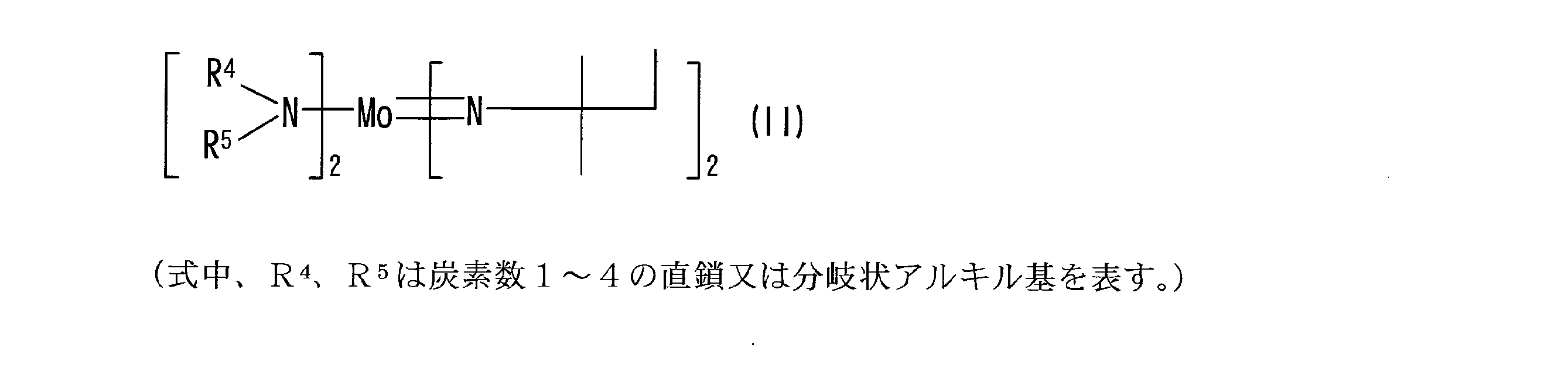
- the present invention also provides a novel compound represented by the following general formula (II).
- the molybdenum amide compound according to the present invention is a low-melting-point compound that becomes liquid at room temperature or slight heating, and has a large temperature difference between the melting point and boiling point, and has a high vapor pressure.
- excellent transportability of the precursor, easy and stable supply of the supply to the substrate is possible, and high-quality thin films containing high-quality molybdenum oxide are manufactured. can do.
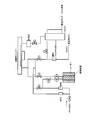
- FIG. 1 is a schematic view showing an example of an apparatus for chemical vapor deposition used in the method for producing a thin film containing molybdenum oxide of the present invention.
- FIG. 2 is a schematic diagram showing another example of an apparatus for chemical vapor deposition used in the method for producing a thin film containing molybdenum oxide of the present invention.
- FIG. 3 is a schematic diagram showing still another example of a chemical vapor deposition apparatus used in the method for producing a thin film containing molybdenum oxide according to the present invention.
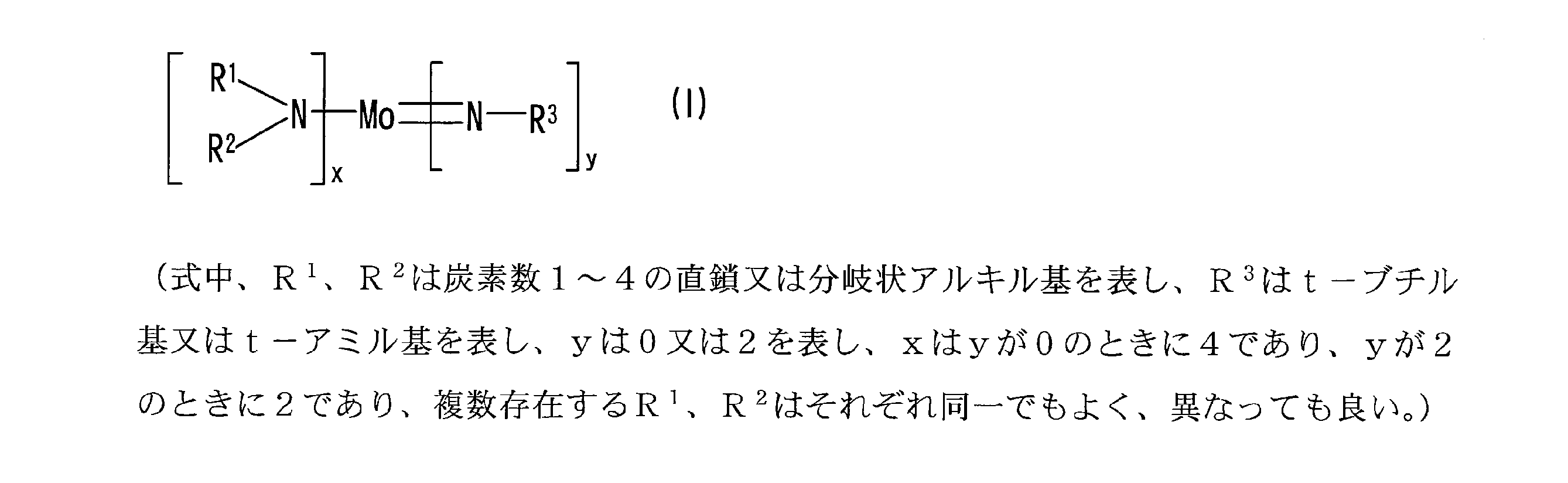
- the linear or branched alkyl group having 1 to 4 carbon atoms represented by R 1 and R 2 is methyl, ethyl, propyl, isopropyl, butyl , S-butyl, t-butyl, isobutyl, R 3 represents t-butyl or t-amyl, y represents 0 or 2, x is 4 when y is 0, and y is When it is 2, it is 2, and a plurality of R 1 and R 2 may be the same or different.
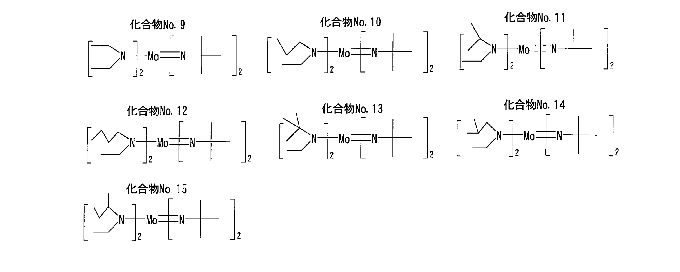
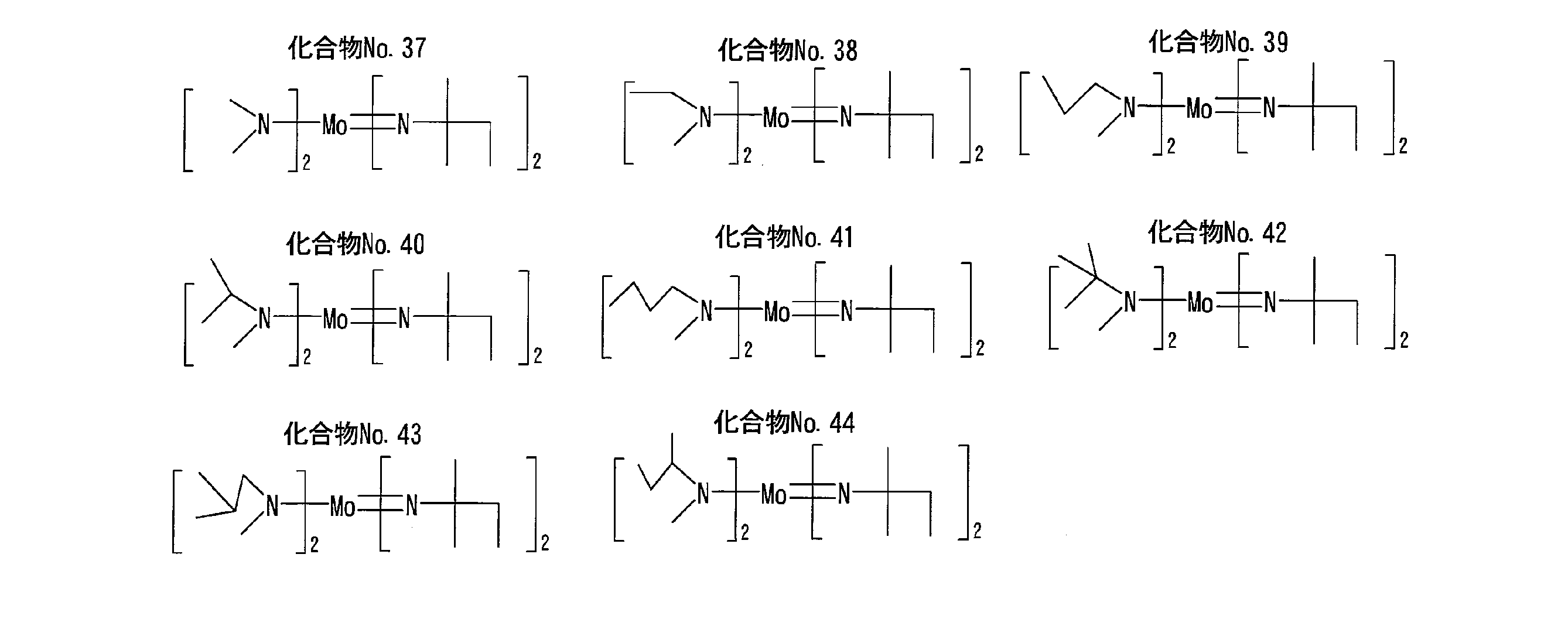
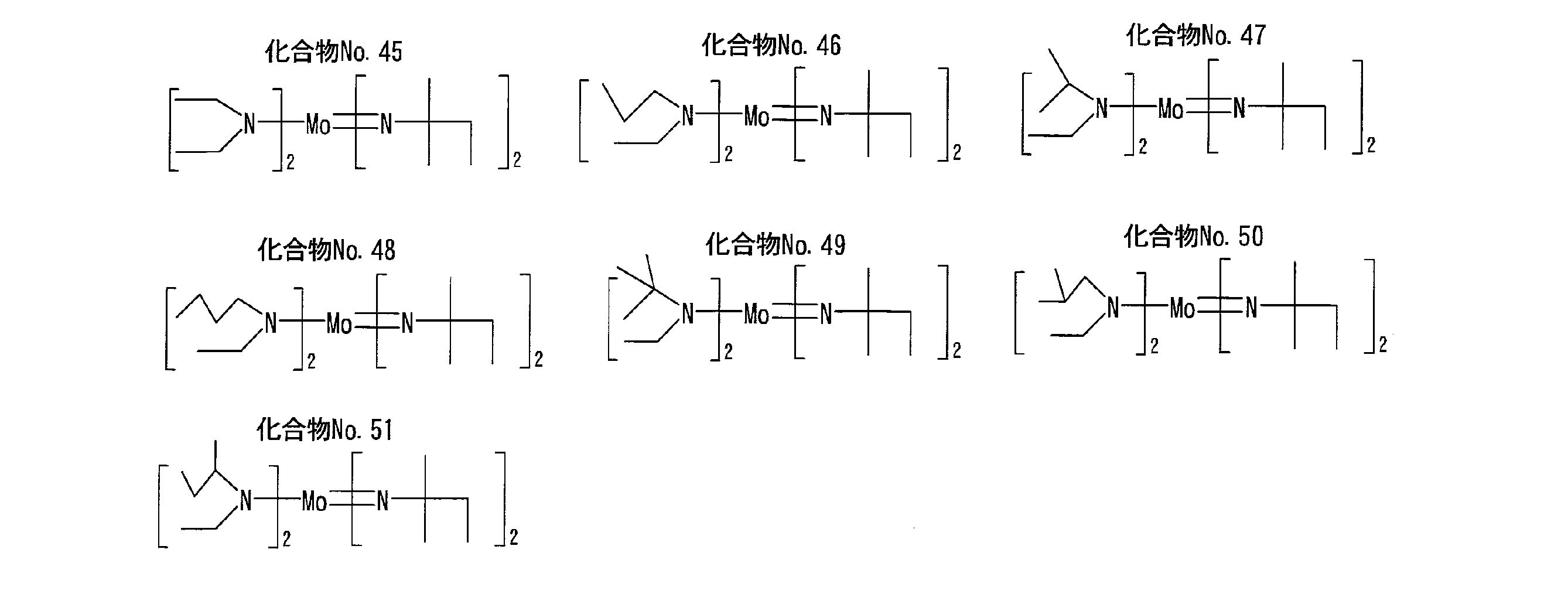
- Specific examples of the molybdenum amide compound, which is a ligand compound having such a group include the following compound Nos. 1 to 81 may be mentioned. However, this invention is not limited at all by the following exemplary compounds.
- R 1 to R 3 in the general formula (I) are preferably those in which the compound is liquid and has a high vapor pressure.
- R 1 and R 2 are preferably a methyl group or an ethyl group
- R 3 is a t-butyl group or a t-amyl group.
- a compound in which R 3 is a t-butyl group has a high vapor pressure and is particularly preferable.
- R 1 and R 2 are preferably a methyl group or an ethyl group.
- the raw material for forming a thin film of the present invention is the above-described molybdenum amide compound used as a precursor for manufacturing a thin film containing molybdenum oxide, and the form varies depending on the process.
- the molybdenum amide compound according to the present invention is particularly useful as a raw material for chemical vapor deposition because of its physical properties.
- the raw material for forming a thin film of the present invention is a raw material for chemical vapor deposition
- the form thereof is appropriately selected according to a method such as a transport supply method of chemical vapor deposition used.
- the chemical vapor deposition raw material is vaporized by heating and / or depressurizing in the raw material container, and together with a carrier gas such as argon, nitrogen, helium, etc. used as needed, to the deposition reaction section.
- a carrier gas such as argon, nitrogen, helium, etc. used as needed.
- the chemical vapor deposition raw material is transported to the vaporization chamber in a liquid or solution state, vaporized by heating and / or decompressing in the vaporization chamber, and then transported to the deposition reaction section
- a carrier gas such as argon, nitrogen, helium, etc.
- the molybdenum amide compound represented by the above general formula (I) itself is a raw material for chemical vapor deposition
- the molybdenum amide compound represented by the above general formula (I) A solution in which the compound itself or the compound is dissolved in an organic solvent becomes a raw material for chemical vapor deposition.
- a chemical vapor deposition material is vaporized and supplied independently for each component (hereinafter sometimes referred to as a single source method), and a multi-component material is previously prepared.
- a method of vaporizing and supplying a mixed raw material mixed in a desired composition hereinafter sometimes referred to as a cocktail sauce method.
- a cocktail sauce method a mixture or a mixed solution of the molybdenum amide compound according to the present invention and another precursor is a raw material for chemical vapor deposition.
- the organic solvent used for the chemical vapor deposition raw material is not particularly limited and a known general organic solvent can be used.
- the organic solvent include acetates such as ethyl acetate, butyl acetate and methoxyethyl acetate; ether alcohols such as ethylene glycol monomethyl ether, ethylene glycol monoethyl ether, ethylene glycol monobutyl ether and diethylene glycol monomethyl ether; tetrahydrofuran, Ethers such as tetrahydropyran, ethylene glycol dimethyl ether, diethylene glycol dimethyl ether, triethylene glycol dimethyl ether, dibutyl ether, dioxane; methyl butyl ketone, methyl isobutyl ketone, ethyl butyl ketone, dipropyl ketone, diisobutyl ketone, methyl amyl ketone, cyclohexanone, methyl Ketones such as cyclo
- the solvent may be used alone or as a mixed solvent of two or more.
- the total amount of the molybdenum amide compound according to the present invention and other precursors in the organic solvent is 0.01 to 2.0 mol / liter, particularly 0.05 to 1.0 mol / liter. It is preferable to make it liter.
- Examples of other precursors include compounds of one or more organic coordination compounds such as alcohol compounds, glycol compounds, ⁇ -diketone compounds, cyclopentadiene compounds, and organic amine compounds, and silicon or metals.
- the precursor metal species include lithium, sodium, potassium, magnesium, calcium, strontium, barium, titanium, zirconium, hafnium, vanadium, niobium, tantalum, molybdenum, manganese, iron, ruthenium, cobalt, rhodium, iridium, nickel.
- Examples of the alcohol compound used as the organic ligand include alkyl alcohols such as methanol, ethanol, propanol, isopropanol, butanol, 2-butanol, isobutanol, t-butanol, amyl alcohol, isoamyl alcohol, and t-amyl alcohol.
- alkyl alcohols such as methanol, ethanol, propanol, isopropanol, butanol, 2-butanol, isobutanol, t-butanol, amyl alcohol, isoamyl alcohol, and t-amyl alcohol.
- glycol compound used as the organic ligand examples include 1,2-ethanediol, 1,2-propanediol, 1,3-propanediol, 2,4-hexanediol, 2,2-dimethyl-1, 3-propanediol, 2,2-diethyl-1,3-propanediol, 1,3-butanediol, 2,4-butanediol, 2,2-diethyl-1,3-butanediol, 2-ethyl-2 -Butyl-1,3-propanediol, 2,4-pentanediol, 2-methyl-1,3-propanediol, 2-methyl-2,4-pentanediol, 2,4-hexanediol, 2,4- Examples include dimethyl-2,4-pentanediol.
- Examples of the ⁇ -diketone compound used as the organic ligand include acetylacetone, hexane-2,4-dione, 5-methylhexane-2,4-dione, heptane-2,4-dione, 2-methylheptane- 3,5-dione, 5-methylheptane-2,4-dione, 6-methylheptane-2,4-dione, 2,2-dimethylheptane-3,5-dione, 2,6-dimethylheptane-3, 5-dione, 2,2,6-trimethylheptane-3,5-dione, 2,2,6,6-tetramethylheptane-3,5-dione, octane-2,4-dione, 2,2,6 -Trimethyloctane-3,5-dione, 2,6-dimethyloctane-3,5-dione, 2,9-dimethylnonane-4,6-dione 2-methyl-6-e
- Examples of the cyclopentadiene compound used as the organic ligand include cyclopentadiene, methylcyclopentadiene, ethylcyclopentadiene, propylcyclopentadiene, isopropylcyclopentadiene, butylcyclopentadiene, s-butylcyclopentadiene, isobutylcyclopentadiene, t-
- Examples of the organic amine compound used as the organic ligand include butylcyclopentadiene, dimethylcyclopentadiene, tetramethylcyclopentadiene, and the like.
- Examples include methylamine, ethylamine, propylamine, isopropylamine, butylamine, s-butylamine, t-butylamine, isobutylamine, dimethylamine, diethylamine, dipropylamine, diisopropylamine, ethylmethylamine, propylmethylamine, isopropylmethylamine It is done.
- the above-mentioned other precursors are preferably compounds having similar thermal and / or oxidative decomposition behavior, and in the case of the cocktail source method, the thermal and / or oxidative decomposition behavior is similar.
- a material that does not undergo alteration due to a chemical reaction during mixing is preferable.
- the raw material for chemical vapor deposition of the present invention should contain as little impurities metal elements as possible, impurities halogen such as impurity chlorine, and organic impurities as much as possible.
- the impurity metal element content is preferably 100 ppb or less for each element, more preferably 10 ppb or less, and the total amount is preferably 1 ppm or less, more preferably 100 ppb or less.
- an alkali metal element, an alkaline earth metal element, or a family element (chromium or tungsten) that affects the electrical characteristics of the obtained thin film. It is necessary to reduce the content.
- the impurity halogen content is preferably 100 ppm or less, more preferably 10 ppm or less, and even more preferably 1 ppm or less.
- the total amount of impurity organic components is preferably 500 ppm or less, more preferably 50 ppm or less, and even more preferably 10 ppm or less.
- each metal compound, organic solvent, and nucleophilic reagent is reduced in moisture. Therefore, it is better to remove moisture as much as possible before use.
- the water content of each of the metal compound, the organic solvent, and the nucleophilic reagent is preferably 10 ppm or less, and more preferably 1 ppm or less.
- the chemical vapor deposition material of the present invention contains as few particles as possible in order to reduce or prevent particle contamination of the thin film to be formed.
- the number of particles larger than 0.3 ⁇ m is preferably 100 or less in 1 ml of the liquid phase, and larger than 0.2 ⁇ m.
- the number of particles is more preferably 1000 or less in 1 ml of the liquid phase, and the number of particles larger than 0.2 ⁇ m is further preferably 100 or less in 1 ml of the liquid phase.
- the method for producing a thin film containing molybdenum oxide according to the present invention comprises a gas containing a molybdenum amide compound obtained by vaporizing the compound represented by the general formula (I), and another precursor used as necessary.
- the vaporized gas and the oxidizing gas are introduced onto the substrate, and then a molybdenum amide compound and other precursors used as necessary are decomposed and / or reacted on the substrate to grow a desired thin film on the substrate.
- This is due to the chemical vapor deposition method used for deposition.
- the oxidizing gas used in the method for producing a thin film containing molybdenum oxide of the present invention includes oxygen, singlet oxygen, ozone, carbon dioxide, nitrogen monoxide, nitrogen dioxide, water, hydrogen peroxide, formic acid, acetic acid, anhydrous An acetic acid etc. are mentioned, These can be used 1 type or 2 or more types. Since the residual carbon in the film can be further reduced, it is preferable to use one containing ozone, oxygen or water as the oxidizing gas.
- examples of the transport and supply method include the gas transport method, the liquid transport method, the single source method, and the cocktail sauce method described above.
- the deposition method includes a thermal CVD method in which a molybdenum amide compound (and other precursor gas) and a reactive gas are reacted only with heat to deposit a thin film, a plasma CVD method using heat and plasma, and heat and light.
- a photo-CVD method using a laser a photo-plasma CVD method using heat, light and plasma
- an ALD method in which the deposition reaction of the CVD method is divided into elementary processes and deposition is performed stepwise at the molecular level.
- examples of the manufacturing conditions include reaction temperature (substrate temperature), reaction pressure, and deposition rate.
- the reaction temperature is preferably 100 ° C. or more, more preferably 100 to 300 ° C., which is the temperature at which the molybdenum amide compound according to the present invention sufficiently reacts.
- the reaction pressure is preferably 0.01 to 300 Pa in the case of the thermal CVD method, the photo CVD method, and the plasma CVD method.
- the deposition rate can be controlled by the raw material supply conditions (vaporization temperature, vaporization pressure), reaction temperature, and reaction pressure. When the deposition rate is large, the properties of the obtained thin film may be deteriorated. When the deposition rate is small, the productivity may be problematic.
- the deposition rate is preferably 0.2 to 40.0 nm / min, and 4.0 to 25.0 nm. / Min is more preferable.
- the number of cycles is controlled so as to obtain a desired film thickness.
- a precursor thin film is formed on the substrate by the molybdenum amide compound introduced into the deposition reaction section after the raw material introduction step described above (precursor thin film). Film forming step). At this time, heat may be applied by heating the substrate or heating the deposition reaction part.
- the precursor thin film formed in this step is a molybdenum amide thin film or a thin film formed by decomposition and / or reaction of a part of the molybdenum amide compound, and has a composition different from that of the target molybdenum oxide thin film.
- the temperature at which this step is performed is preferably from room temperature to 500 ° C, more preferably from 100 to 300 ° C.
- unreacted molybdenum amide compound gas and by-product gas are exhausted from the deposition reaction part (exhaust process).
- the unreacted molybdenum amide compound gas or by-product gas is completely exhausted from the deposition reaction part, but it is not necessarily exhausted completely.
- the exhaust method include a method of purging the system with an inert gas such as helium and argon, a method of exhausting the system by depressurizing the system, a method combining these, and the like.
- the degree of pressure reduction is preferably 0.01 to 300 Pa, more preferably 0.1 to 100 Pa.
- an oxidizing gas is introduced into the deposition reaction portion, and a molybdenum oxide thin film is formed from the precursor thin film obtained in the precursor thin film forming step by the action of the oxidizing gas or the oxidizing gas and heat.
- the temperature when heat is applied in this step is preferably room temperature to 500 ° C, more preferably 100 to 300 ° C.
- the molybdenum amide compound according to the present invention has good reactivity with an oxidizing gas, and a molybdenum oxide thin film can be obtained.
- Thin film deposition by a series of operations consisting of the above-described raw material introduction process, precursor thin film formation process, exhaust process, and molybdenum oxide thin film formation process is defined as one cycle, and this cycle is repeated until a thin film having a required film thickness is obtained. May be repeated. In this case, after one cycle is performed, the next cycle is performed after exhausting unreacted molybdenum amide compound gas, oxidizing gas, and by-product gas from the deposition reaction portion in the same manner as the exhaust process. Is preferred.
- energy such as plasma, light, or voltage may be applied.
- the timing for applying these energies is not particularly limited. For example, when introducing a molybdenum amide compound gas in the raw material introduction process, heating in the molybdenum oxide thin film formation process or molybdenum oxide thin film formation process, and in the exhaust process At the time of evacuation, it may be at the time of introducing an oxidizing gas in the molybdenum oxide thin film forming step, or may be between the above steps.
- annealing may be performed in an inert atmosphere, an oxidizing gas or a reducing gas atmosphere in order to obtain better film quality, and step filling is necessary.
- a reflow process may be provided.
- the temperature is preferably 400 to 1200 ° C., particularly preferably 500 to 800 ° C.
- a known chemical vapor deposition apparatus can be used as the apparatus used in the method for producing a thin film of the present invention.
- the apparatus include a non-shower head type apparatus as shown in FIG. 1, an apparatus capable of carrying a precursor as shown in FIG. 2 by bubbling supply, and an apparatus having a vaporization chamber as shown in FIG. It is done.
- an apparatus capable of simultaneously processing a large number of sheets using a batch furnace can also be used.
- Examples of the thin film containing molybdenum oxide formed and manufactured using the chemical vapor deposition raw material of the present invention include molybdenum dioxide, molybdenum trioxide, molybdenum-sodium composite oxide, molybdenum-calcium composite oxide, Molybdenum-bismuth complex oxide, molybdenum-niobium complex oxide, molybdenum-zinc complex oxide, molybdenum-silicon complex oxide, molybdenum-cerium complex oxide, and these applications include electrodes, In addition to electronic parts such as barrier films, catalysts, catalyst raw materials, metal raw materials, metal surface treatment agents, ceramic additives, sintered metal additives, flame retardants, smoke reducing agents, antifreeze liquid raw materials, inorganic pigments Color formers, basic dye mordants, rust preventive raw materials, agricultural trace fertilizers, and ceramic auxiliary materials.
- the molybdenum amide compound according to the present invention is not particularly limited by the production method, and is produced by applying a known reaction.
- a production method a well-known general method for synthesizing metal amide compounds using the corresponding amide compound may be applied.
- a reactive intermediate is obtained by reacting molybdenum sodium salt, amine and trimethylchlorosilane in 1,2-dimethoxyethane, and then reacting with a dialkylamine.
- Examples of the reactive intermediate include molybdenum imide compounds represented by the following general formula (III).
- the following general formula obtained by reacting a reactive intermediate in which R 6 is a t-amyl group with a dialkylamine does not have a halogen atom typified by fluorine in its structure, and has a high vapor pressure or a low melting point compound that becomes liquid by slight heating. Therefore, in the production of thin films containing molybdenum oxide by chemical vapor deposition, it is useful as a raw material for chemical vapor deposition because it does not corrode devices due to reaction by-products, and is excellent in vaporization and precursor transport. It is.
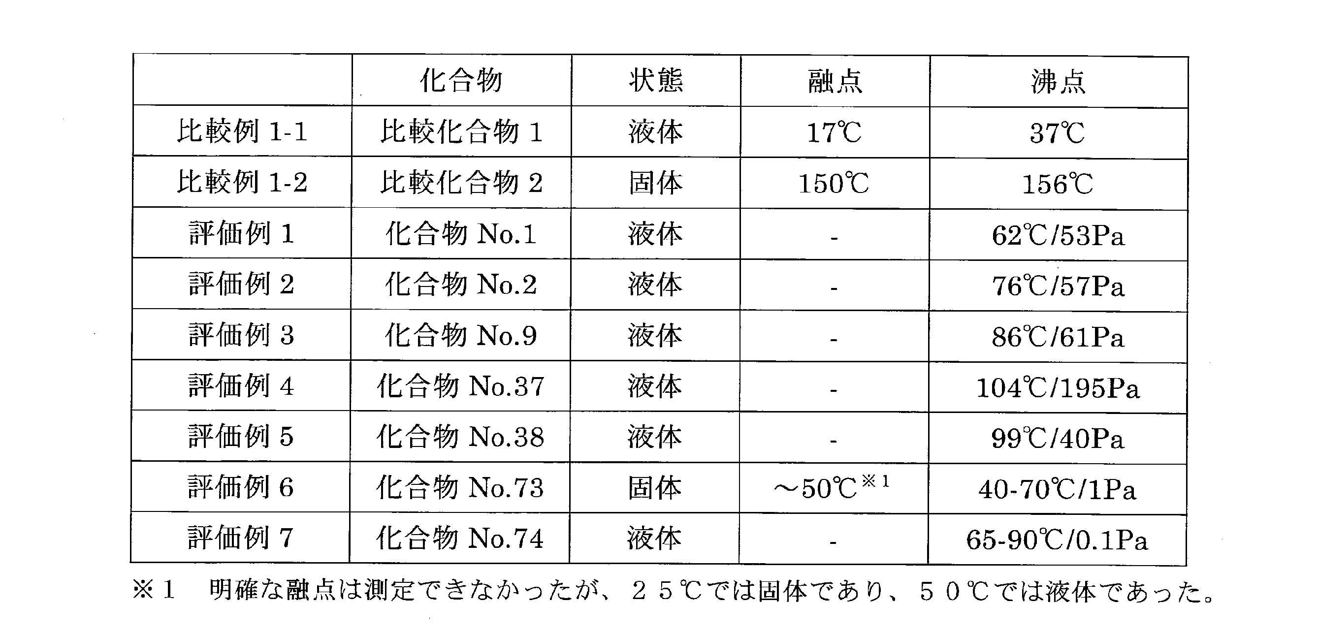
- Comparative Example 1-2 was a solid, whereas Evaluation Examples 1 to 7 were liquids or low melting point compounds that became liquid by slight heating. Further, it was confirmed that the boiling points of Comparative Examples 1-1 and 1-2 and Evaluation Examples 1 to 5 were low.
- the comparative compounds 1 and 2 have low boiling points, the comparative compound 1 has a small difference between the melting point and the boiling point, and it is difficult to stably supply the raw material in a liquid state, and as a reaction by-product during film formation. There is a problem that the device is corroded by the generation of hydrogen fluoride, and Comparative Compound 2 has a smaller difference between the melting point and boiling point than Comparative Compound 1, and can stably supply the raw material in a liquid state.
- the molybdenum amide compound according to the present invention does not contain a halogen atom typified by a fluorine atom in the structure, and further has a large temperature difference between the melting point and the boiling point, so that it can be stably maintained in a liquid state. It was confirmed that it is suitable as a raw material for growth.
- Example 1 Production of molybdenum oxide thin film by ALD method A molybdenum oxide thin film was produced on a silicon wafer by the ALD method under the following conditions and steps using the apparatus shown in FIG. About the obtained thin film, the film thickness measurement by fluorescent X-rays, the composition ratio analysis by X-ray photoelectron spectroscopy, and the composition analysis by X-ray diffraction were performed. The results are shown in Table 3. (conditions) Reaction temperature (substrate temperature); 240 ° C., reactive gas; ozone gas (process) A series of steps consisting of the following (1) to (4) was taken as one cycle and repeated 50 cycles.
- the compound is a low melting point compound that becomes liquid at room temperature and normal pressure or becomes liquid by slight heating. Therefore, it was found that a molybdenum oxide thin film having excellent precursor transportability and supply property, and high productivity and good film quality can be produced.
Landscapes
- Chemical & Material Sciences (AREA)
- Organic Chemistry (AREA)
- Materials Engineering (AREA)
- General Chemical & Material Sciences (AREA)
- Chemical Kinetics & Catalysis (AREA)
- Engineering & Computer Science (AREA)
- Mechanical Engineering (AREA)
- Metallurgy (AREA)
- Inorganic Chemistry (AREA)
- Chemical Vapour Deposition (AREA)
- Electrodes Of Semiconductors (AREA)
- Organic Low-Molecular-Weight Compounds And Preparation Thereof (AREA)
- Composite Materials (AREA)
Abstract
Description






化合物No.37の製造
乾燥アルゴンガス雰囲気下で、500mL反応フラスコにモリブデン酸ナトリウム0.12モル、1,2-ジメトキシエタン2.52モル、t-アミルアミン0.252モル、トリエチルアミン0.48モル、トリメチルクロロシラン0.96モルを仕込み、系内の温度を80~82℃にコントロールして12時間攪拌を行った。反応液を0.2μmのフィルターで固形分をろ過した後、溶媒を減圧留去により濃縮することで深緑色スラリー状の反応性中間体を収率95%で得た。引き続き、反応フラスコに反応性中間体0.114モルと脱水処理を行ったトルエン1.12モルを加えて溶解した後、溶液を-20℃にドライアイス―イソプロパノールにより冷却し、ジメチルアミンガス0.48モルを吹き込み、続いて1.6mol/Lノルマルブチルリチウムのヘキサン溶液140mLを滴下して反応させた。反応溶液を徐々に室温へ戻し、引き続き2時間撹拌して反応させた。反応液を0.2μmのフィルターにより固形物をろ過後、溶媒を減圧留去により濃縮し、これからさらに減圧蒸留により195Pa、塔頂温度103~104℃のフラクションを分取し、目的物である化合物No.37を得た。この精製による回収率は60%であった。得られた橙黄色液体について、以下の分析を行った。
(1)元素分析(金属分析:ICP-AES、塩素分析:TOX)
モリブデン;26.89質量%(理論値27.07%)、Na;1ppm未満、Cl;5ppm未満
(2)1H-NMR(溶媒:重ベンゼン)(ケミカルシフト:多重度:H数)
(1.06:t:3)(1.35:s:6)(1.62:q:2)(3.46:s:6)
(3)TG-DTA
(Ar100ml/min、10℃/min昇温、サンプル量8.836mg)
50質量%減少温度190℃
化合物No.38の製造
乾燥アルゴンガス雰囲気下で、500mL反応フラスコにモリブデン酸ナトリウム0.12モル、1,2-ジメトキシエタン2.52モル、t-アミルアミン0.252モル、トリエチルアミン0.48モル、トリメチルクロロシラン0.96モルを仕込み、系内の温度を80~82℃にコントロールして12時間攪拌を行った。反応液を0.2μmのフィルターで固形分をろ過した後、溶媒を減圧留去により濃縮することで深緑色スラリー状の反応性中間体を収率95%で得た。引き続き、反応フラスコに反応性中間体0.114モルと脱水処理を行ったトルエン1.12モルを加えて溶解した後、溶液を-20℃にドライアイス―イソプロパノールにより冷却し、エチルメチルアミン0.48モルを滴下、続いて1.6mol/Lノルマルブチルリチウムのヘキサン溶液140mLを滴下して反応させた。反応溶液を徐々に室温へ戻し、引き続き2時間撹拌して反応させた。反応液を0.2μmのフィルターにより固形物をろ過後、溶媒を減圧留去により濃縮し、これからさらに減圧蒸留により40Pa、塔頂温度98~101℃のフラクションを分取し、目的物である化合物No.38を得た。この精製よる回収率は60%であった。得られた黄色液体について、以下の分析を行った。
(1)元素分析(金属分析:ICP-AES、塩素分析:TOX)
モリブデン;25.31質量%(理論値25.09%)、Na;1ppm未満、Cl;5ppm未満
(2)1H-NMR(溶媒:重ベンゼン)(ケミカルシフト:多重度:H数)
(1.02:t:2)(1.30:s:9)(1.59:q:3)(3.47:s:3)(3.67:q:2)
(3)TG-DTA
(Ar100ml/min、10℃/min昇温、サンプル量12.009mg)
50質量%減少温度209℃
上記製造実施例により得られた新規化合物No.37、38、公知化合物である化合物No.1、2、9、73、74及び以下に示す比較化合物1、2について、目視によって常温常圧における化合物の状態を観察し、固体化合物については微小融点測定装置を用いて融点を測定し、さらに各化合物の沸点を測定した。結果を表1に示す。
MoF6
比較化合物 2
Mo(CO)6
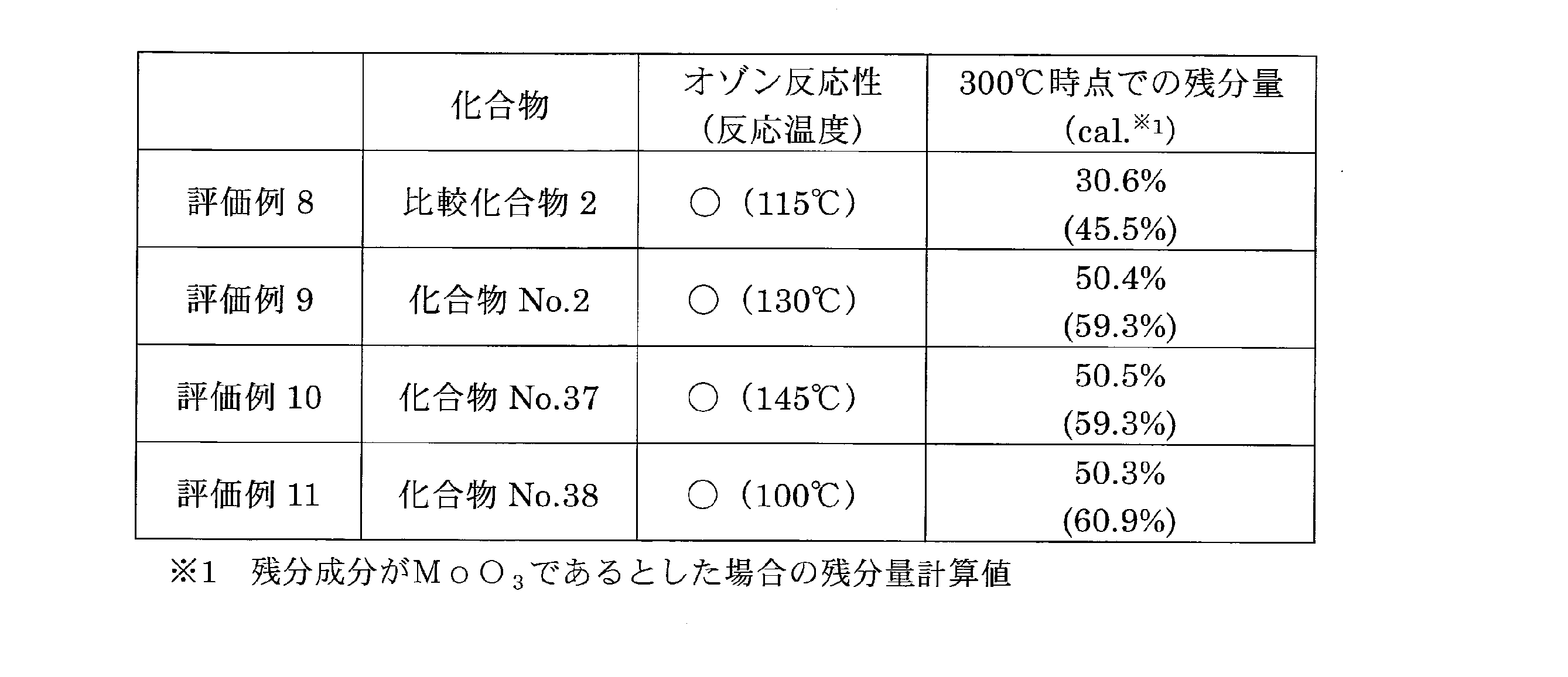
比較化合物2、化合物No.2、及び化合物No.37、38についてオゾン雰囲気下でTG-DTA測定を実施した。測定条件はオゾン4%を添加した酸素2000ml/min、10℃/min昇温で行った。モリブデン化合物とオゾンとの反応性の有無を、オゾンによるモリブデン化合物の酸化分解によって発生する重量減少を伴う発熱ピークの有無によって確認し、さらに反応が十分に終了したと考えられる300℃における残分量を確認した。尚、サンプル量は3.275mg~8.447mgであった。この結果を表2に示す。
化合物No.2を化学気相成長用原料とし、図1に示す装置を用いて以下の条件及び工程のALD法により、シリコンウエハ上に酸化モリブデン薄膜を製造した。得られた薄膜について、蛍光X線による膜厚測定及びX線光電子分光法による組成比分析、X線回折による組成分析を行った。結果を表3に示す。
(条件)
反応温度(基板温度);240℃、反応性ガス;オゾンガス
(工程)
下記(1)~(4)からなる一連の工程を1サイクルとして、50サイクル繰り返した。
(1)気化室温度70℃、気化室圧力70Paの条件で気化させた化学気相成長用原料の蒸気を導入し、系圧100Paで20秒間堆積させる。
(2)15秒間のアルゴンパージにより、未反応原料を除去する。
(3)反応性ガスを導入し、系圧力80Paで20秒間反応させる。
(4)15秒間のアルゴンパージにより、未反応原料を除去する。

Claims (4)
- 下記一般式(I)で表される化合物を含有してなる薄膜形成用原料を気化させて得たモリブデンアミド化合物を含有する蒸気を基体上に導入し、さらに酸化性ガスを導入することで分解及び/又は化学反応させて基体上に薄膜を形成する、酸化モリブデンを含有する薄膜の製造方法。

- 上記酸化性ガスがオゾン、酸素又は水を含むガスである請求項1に記載の酸化モリブデンを含有する薄膜の製造方法。
- 請求項1又は2に記載の薄膜の製造方法に使用する下記一般式(I)で表される化合物を含有してなる、酸化モリブデンを含有する薄膜の形成用原料。
- 下記一般式(II)で表される化合物。
Priority Applications (4)
| Application Number | Priority Date | Filing Date | Title |
|---|---|---|---|
| US14/112,125 US20140141165A1 (en) | 2011-05-27 | 2012-05-11 | Method for manufacturing molybdenum oxide-containing thin film, starting material for forming molybdenum oxide-containing thin film, and molybdenum amide compound |
| KR1020137027972A KR101912127B1 (ko) | 2011-05-27 | 2012-05-11 | 산화몰리브덴을 함유하는 박막의 제조방법, 산화몰리브덴을 함유하는 박막의 형성용 원료 및 몰리브덴아미드 화합물 |
| CN201280020076.XA CN103562434A (zh) | 2011-05-27 | 2012-05-11 | 含有氧化钼的薄膜的制造方法、含有氧化钼的薄膜的形成用原料以及钼酰胺化合物 |
| US14/823,293 US9881796B2 (en) | 2011-05-27 | 2015-08-11 | Method for manufacturing molybdenum oxide-containing thin film |
Applications Claiming Priority (2)
| Application Number | Priority Date | Filing Date | Title |
|---|---|---|---|
| JP2011-118760 | 2011-05-27 | ||
| JP2011118760A JP5730670B2 (ja) | 2011-05-27 | 2011-05-27 | 酸化モリブデンを含有する薄膜の製造方法、及び酸化モリブデンを含有する薄膜の形成用原料 |
Related Child Applications (2)
| Application Number | Title | Priority Date | Filing Date |
|---|---|---|---|
| US14/112,125 A-371-Of-International US20140141165A1 (en) | 2011-05-27 | 2012-05-11 | Method for manufacturing molybdenum oxide-containing thin film, starting material for forming molybdenum oxide-containing thin film, and molybdenum amide compound |
| US14/823,293 Division US9881796B2 (en) | 2011-05-27 | 2015-08-11 | Method for manufacturing molybdenum oxide-containing thin film |
Publications (1)
| Publication Number | Publication Date |
|---|---|
| WO2012165124A1 true WO2012165124A1 (ja) | 2012-12-06 |
Family
ID=47258988
Family Applications (1)
| Application Number | Title | Priority Date | Filing Date |
|---|---|---|---|
| PCT/JP2012/062199 Ceased WO2012165124A1 (ja) | 2011-05-27 | 2012-05-11 | 酸化モリブデンを含有する薄膜の製造方法、酸化モリブデンを含有する薄膜の形成用原料及びモリブデンアミド化合物 |
Country Status (6)
| Country | Link |
|---|---|
| US (2) | US20140141165A1 (ja) |
| JP (1) | JP5730670B2 (ja) |
| KR (1) | KR101912127B1 (ja) |
| CN (1) | CN103562434A (ja) |
| TW (1) | TWI546308B (ja) |
| WO (1) | WO2012165124A1 (ja) |
Families Citing this family (370)
| Publication number | Priority date | Publication date | Assignee | Title |
|---|---|---|---|---|
| US9394608B2 (en) | 2009-04-06 | 2016-07-19 | Asm America, Inc. | Semiconductor processing reactor and components thereof |
| US8802201B2 (en) | 2009-08-14 | 2014-08-12 | Asm America, Inc. | Systems and methods for thin-film deposition of metal oxides using excited nitrogen-oxygen species |
| US9312155B2 (en) | 2011-06-06 | 2016-04-12 | Asm Japan K.K. | High-throughput semiconductor-processing apparatus equipped with multiple dual-chamber modules |
| US10854498B2 (en) | 2011-07-15 | 2020-12-01 | Asm Ip Holding B.V. | Wafer-supporting device and method for producing same |
| US20130023129A1 (en) | 2011-07-20 | 2013-01-24 | Asm America, Inc. | Pressure transmitter for a semiconductor processing environment |
| US9017481B1 (en) | 2011-10-28 | 2015-04-28 | Asm America, Inc. | Process feed management for semiconductor substrate processing |
| US10714315B2 (en) | 2012-10-12 | 2020-07-14 | Asm Ip Holdings B.V. | Semiconductor reaction chamber showerhead |
| WO2014077073A1 (ja) * | 2012-11-19 | 2014-05-22 | 株式会社Adeka | モリブデンを含有する薄膜の製造方法、薄膜形成用原料及びモリブデンイミド化合物 |
| US20160376700A1 (en) | 2013-02-01 | 2016-12-29 | Asm Ip Holding B.V. | System for treatment of deposition reactor |
| US10683571B2 (en) | 2014-02-25 | 2020-06-16 | Asm Ip Holding B.V. | Gas supply manifold and method of supplying gases to chamber using same |
| US10167557B2 (en) | 2014-03-18 | 2019-01-01 | Asm Ip Holding B.V. | Gas distribution system, reactor including the system, and methods of using the same |
| US11015245B2 (en) | 2014-03-19 | 2021-05-25 | Asm Ip Holding B.V. | Gas-phase reactor and system having exhaust plenum and components thereof |
| TW201606115A (zh) * | 2014-07-07 | 2016-02-16 | 液態空氣喬治斯克勞帝方法研究開發股份有限公司 | 用於薄膜沉積之含鉬及鎢之前驅物 |
| US10858737B2 (en) | 2014-07-28 | 2020-12-08 | Asm Ip Holding B.V. | Showerhead assembly and components thereof |
| TWI656232B (zh) * | 2014-08-14 | 2019-04-11 | 法商液態空氣喬治斯克勞帝方法研究開發股份有限公司 | 鉬組成物及其用於形成氧化鉬膜之用途 |
| US9890456B2 (en) | 2014-08-21 | 2018-02-13 | Asm Ip Holding B.V. | Method and system for in situ formation of gas-phase compounds |
| US10941490B2 (en) | 2014-10-07 | 2021-03-09 | Asm Ip Holding B.V. | Multiple temperature range susceptor, assembly, reactor and system including the susceptor, and methods of using the same |
| US9657845B2 (en) | 2014-10-07 | 2017-05-23 | Asm Ip Holding B.V. | Variable conductance gas distribution apparatus and method |
| JP5913663B2 (ja) * | 2015-02-19 | 2016-04-27 | 株式会社Adeka | モリブデンアミド化合物 |
| US10276355B2 (en) | 2015-03-12 | 2019-04-30 | Asm Ip Holding B.V. | Multi-zone reactor, system including the reactor, and method of using the same |
| KR102314722B1 (ko) * | 2015-05-27 | 2021-10-20 | 에이에스엠 아이피 홀딩 비.브이. | 몰리브덴 또는 텅스텐 함유 박막의 ald용 전구체의 합성 및 사용 |
| US10458018B2 (en) | 2015-06-26 | 2019-10-29 | Asm Ip Holding B.V. | Structures including metal carbide material, devices including the structures, and methods of forming same |
| US10600673B2 (en) | 2015-07-07 | 2020-03-24 | Asm Ip Holding B.V. | Magnetic susceptor to baseplate seal |
| US10211308B2 (en) | 2015-10-21 | 2019-02-19 | Asm Ip Holding B.V. | NbMC layers |
| US11139308B2 (en) | 2015-12-29 | 2021-10-05 | Asm Ip Holding B.V. | Atomic layer deposition of III-V compounds to form V-NAND devices |
| US10529554B2 (en) | 2016-02-19 | 2020-01-07 | Asm Ip Holding B.V. | Method for forming silicon nitride film selectively on sidewalls or flat surfaces of trenches |
| US10343920B2 (en) | 2016-03-18 | 2019-07-09 | Asm Ip Holding B.V. | Aligned carbon nanotubes |
| CN109449316B (zh) * | 2016-04-19 | 2020-04-17 | Tcl集团股份有限公司 | 一种In掺杂MoO3薄膜的制备方法 |
| US10865475B2 (en) | 2016-04-21 | 2020-12-15 | Asm Ip Holding B.V. | Deposition of metal borides and silicides |
| US10190213B2 (en) | 2016-04-21 | 2019-01-29 | Asm Ip Holding B.V. | Deposition of metal borides |
| US10367080B2 (en) | 2016-05-02 | 2019-07-30 | Asm Ip Holding B.V. | Method of forming a germanium oxynitride film |
| US10032628B2 (en) | 2016-05-02 | 2018-07-24 | Asm Ip Holding B.V. | Source/drain performance through conformal solid state doping |
| US11453943B2 (en) | 2016-05-25 | 2022-09-27 | Asm Ip Holding B.V. | Method for forming carbon-containing silicon/metal oxide or nitride film by ALD using silicon precursor and hydrocarbon precursor |
| US10662527B2 (en) | 2016-06-01 | 2020-05-26 | Asm Ip Holding B.V. | Manifolds for uniform vapor deposition |
| US9859151B1 (en) | 2016-07-08 | 2018-01-02 | Asm Ip Holding B.V. | Selective film deposition method to form air gaps |
| US10612137B2 (en) | 2016-07-08 | 2020-04-07 | Asm Ip Holdings B.V. | Organic reactants for atomic layer deposition |
| WO2018013778A1 (en) * | 2016-07-14 | 2018-01-18 | Entegris, Inc. | Cvd mo deposition by using mooc14 |
| US10714385B2 (en) | 2016-07-19 | 2020-07-14 | Asm Ip Holding B.V. | Selective deposition of tungsten |
| US9812320B1 (en) | 2016-07-28 | 2017-11-07 | Asm Ip Holding B.V. | Method and apparatus for filling a gap |
| KR102532607B1 (ko) | 2016-07-28 | 2023-05-15 | 에이에스엠 아이피 홀딩 비.브이. | 기판 가공 장치 및 그 동작 방법 |
| US9887082B1 (en) | 2016-07-28 | 2018-02-06 | Asm Ip Holding B.V. | Method and apparatus for filling a gap |
| US10573522B2 (en) | 2016-08-16 | 2020-02-25 | Lam Research Corporation | Method for preventing line bending during metal fill process |
| US10358407B2 (en) | 2016-10-12 | 2019-07-23 | Asm Ip Holding B.V. | Synthesis and use of precursors for vapor deposition of tungsten containing thin films |
| US10643826B2 (en) | 2016-10-26 | 2020-05-05 | Asm Ip Holdings B.V. | Methods for thermally calibrating reaction chambers |
| US11532757B2 (en) | 2016-10-27 | 2022-12-20 | Asm Ip Holding B.V. | Deposition of charge trapping layers |
| US10714350B2 (en) | 2016-11-01 | 2020-07-14 | ASM IP Holdings, B.V. | Methods for forming a transition metal niobium nitride film on a substrate by atomic layer deposition and related semiconductor device structures |
| US10229833B2 (en) | 2016-11-01 | 2019-03-12 | Asm Ip Holding B.V. | Methods for forming a transition metal nitride film on a substrate by atomic layer deposition and related semiconductor device structures |
| US10643904B2 (en) | 2016-11-01 | 2020-05-05 | Asm Ip Holdings B.V. | Methods for forming a semiconductor device and related semiconductor device structures |
| US10134757B2 (en) | 2016-11-07 | 2018-11-20 | Asm Ip Holding B.V. | Method of processing a substrate and a device manufactured by using the method |
| KR102546317B1 (ko) | 2016-11-15 | 2023-06-21 | 에이에스엠 아이피 홀딩 비.브이. | 기체 공급 유닛 및 이를 포함하는 기판 처리 장치 |
| KR102762543B1 (ko) | 2016-12-14 | 2025-02-05 | 에이에스엠 아이피 홀딩 비.브이. | 기판 처리 장치 |
| US11447861B2 (en) | 2016-12-15 | 2022-09-20 | Asm Ip Holding B.V. | Sequential infiltration synthesis apparatus and a method of forming a patterned structure |
| US11581186B2 (en) | 2016-12-15 | 2023-02-14 | Asm Ip Holding B.V. | Sequential infiltration synthesis apparatus |
| KR102700194B1 (ko) | 2016-12-19 | 2024-08-28 | 에이에스엠 아이피 홀딩 비.브이. | 기판 처리 장치 |
| US10269558B2 (en) | 2016-12-22 | 2019-04-23 | Asm Ip Holding B.V. | Method of forming a structure on a substrate |
| US10867788B2 (en) | 2016-12-28 | 2020-12-15 | Asm Ip Holding B.V. | Method of forming a structure on a substrate |
| US11390950B2 (en) | 2017-01-10 | 2022-07-19 | Asm Ip Holding B.V. | Reactor system and method to reduce residue buildup during a film deposition process |
| US10655221B2 (en) | 2017-02-09 | 2020-05-19 | Asm Ip Holding B.V. | Method for depositing oxide film by thermal ALD and PEALD |
| US10468261B2 (en) | 2017-02-15 | 2019-11-05 | Asm Ip Holding B.V. | Methods for forming a metallic film on a substrate by cyclical deposition and related semiconductor device structures |
| US10529563B2 (en) | 2017-03-29 | 2020-01-07 | Asm Ip Holdings B.V. | Method for forming doped metal oxide films on a substrate by cyclical deposition and related semiconductor device structures |
| USD876504S1 (en) | 2017-04-03 | 2020-02-25 | Asm Ip Holding B.V. | Exhaust flow control ring for semiconductor deposition apparatus |
| CN118366851A (zh) * | 2017-04-10 | 2024-07-19 | 朗姆研究公司 | 含钼的低电阻率的膜 |
| KR102457289B1 (ko) | 2017-04-25 | 2022-10-21 | 에이에스엠 아이피 홀딩 비.브이. | 박막 증착 방법 및 반도체 장치의 제조 방법 |
| US10892156B2 (en) | 2017-05-08 | 2021-01-12 | Asm Ip Holding B.V. | Methods for forming a silicon nitride film on a substrate and related semiconductor device structures |
| US10770286B2 (en) | 2017-05-08 | 2020-09-08 | Asm Ip Holdings B.V. | Methods for selectively forming a silicon nitride film on a substrate and related semiconductor device structures |
| US12040200B2 (en) | 2017-06-20 | 2024-07-16 | Asm Ip Holding B.V. | Semiconductor processing apparatus and methods for calibrating a semiconductor processing apparatus |
| US11306395B2 (en) | 2017-06-28 | 2022-04-19 | Asm Ip Holding B.V. | Methods for depositing a transition metal nitride film on a substrate by atomic layer deposition and related deposition apparatus |
| US10685834B2 (en) | 2017-07-05 | 2020-06-16 | Asm Ip Holdings B.V. | Methods for forming a silicon germanium tin layer and related semiconductor device structures |
| KR20190009245A (ko) | 2017-07-18 | 2019-01-28 | 에이에스엠 아이피 홀딩 비.브이. | 반도체 소자 구조물 형성 방법 및 관련된 반도체 소자 구조물 |
| US11018002B2 (en) | 2017-07-19 | 2021-05-25 | Asm Ip Holding B.V. | Method for selectively depositing a Group IV semiconductor and related semiconductor device structures |
| US10541333B2 (en) | 2017-07-19 | 2020-01-21 | Asm Ip Holding B.V. | Method for depositing a group IV semiconductor and related semiconductor device structures |
| US11374112B2 (en) | 2017-07-19 | 2022-06-28 | Asm Ip Holding B.V. | Method for depositing a group IV semiconductor and related semiconductor device structures |
| US10590535B2 (en) | 2017-07-26 | 2020-03-17 | Asm Ip Holdings B.V. | Chemical treatment, deposition and/or infiltration apparatus and method for using the same |
| TWI815813B (zh) | 2017-08-04 | 2023-09-21 | 荷蘭商Asm智慧財產控股公司 | 用於分配反應腔內氣體的噴頭總成 |
| US10692741B2 (en) | 2017-08-08 | 2020-06-23 | Asm Ip Holdings B.V. | Radiation shield |
| US10770336B2 (en) | 2017-08-08 | 2020-09-08 | Asm Ip Holding B.V. | Substrate lift mechanism and reactor including same |
| US11139191B2 (en) | 2017-08-09 | 2021-10-05 | Asm Ip Holding B.V. | Storage apparatus for storing cassettes for substrates and processing apparatus equipped therewith |
| US11769682B2 (en) | 2017-08-09 | 2023-09-26 | Asm Ip Holding B.V. | Storage apparatus for storing cassettes for substrates and processing apparatus equipped therewith |
| US10249524B2 (en) | 2017-08-09 | 2019-04-02 | Asm Ip Holding B.V. | Cassette holder assembly for a substrate cassette and holding member for use in such assembly |
| USD900036S1 (en) | 2017-08-24 | 2020-10-27 | Asm Ip Holding B.V. | Heater electrical connector and adapter |
| US11830730B2 (en) | 2017-08-29 | 2023-11-28 | Asm Ip Holding B.V. | Layer forming method and apparatus |
| US20190067003A1 (en) * | 2017-08-30 | 2019-02-28 | Asm Ip Holding B.V. | Methods for depositing a molybdenum metal film on a dielectric surface of a substrate and related semiconductor device structures |
| KR102491945B1 (ko) | 2017-08-30 | 2023-01-26 | 에이에스엠 아이피 홀딩 비.브이. | 기판 처리 장치 |
| US11295980B2 (en) | 2017-08-30 | 2022-04-05 | Asm Ip Holding B.V. | Methods for depositing a molybdenum metal film over a dielectric surface of a substrate by a cyclical deposition process and related semiconductor device structures |
| US11056344B2 (en) | 2017-08-30 | 2021-07-06 | Asm Ip Holding B.V. | Layer forming method |
| KR102401446B1 (ko) | 2017-08-31 | 2022-05-24 | 에이에스엠 아이피 홀딩 비.브이. | 기판 처리 장치 |
| US10607895B2 (en) * | 2017-09-18 | 2020-03-31 | Asm Ip Holdings B.V. | Method for forming a semiconductor device structure comprising a gate fill metal |
| KR102630301B1 (ko) | 2017-09-21 | 2024-01-29 | 에이에스엠 아이피 홀딩 비.브이. | 침투성 재료의 순차 침투 합성 방법 처리 및 이를 이용하여 형성된 구조물 및 장치 |
| US10844484B2 (en) | 2017-09-22 | 2020-11-24 | Asm Ip Holding B.V. | Apparatus for dispensing a vapor phase reactant to a reaction chamber and related methods |
| US10658205B2 (en) | 2017-09-28 | 2020-05-19 | Asm Ip Holdings B.V. | Chemical dispensing apparatus and methods for dispensing a chemical to a reaction chamber |
| US10403504B2 (en) | 2017-10-05 | 2019-09-03 | Asm Ip Holding B.V. | Method for selectively depositing a metallic film on a substrate |
| US10319588B2 (en) | 2017-10-10 | 2019-06-11 | Asm Ip Holding B.V. | Method for depositing a metal chalcogenide on a substrate by cyclical deposition |
| US10923344B2 (en) | 2017-10-30 | 2021-02-16 | Asm Ip Holding B.V. | Methods for forming a semiconductor structure and related semiconductor structures |
| KR102443047B1 (ko) | 2017-11-16 | 2022-09-14 | 에이에스엠 아이피 홀딩 비.브이. | 기판 처리 장치 방법 및 그에 의해 제조된 장치 |
| US10910262B2 (en) | 2017-11-16 | 2021-02-02 | Asm Ip Holding B.V. | Method of selectively depositing a capping layer structure on a semiconductor device structure |
| US11022879B2 (en) | 2017-11-24 | 2021-06-01 | Asm Ip Holding B.V. | Method of forming an enhanced unexposed photoresist layer |
| JP7206265B2 (ja) | 2017-11-27 | 2023-01-17 | エーエスエム アイピー ホールディング ビー.ブイ. | クリーン・ミニエンバイロメントを備える装置 |
| CN111316417B (zh) | 2017-11-27 | 2023-12-22 | 阿斯莫Ip控股公司 | 与批式炉偕同使用的用于储存晶圆匣的储存装置 |
| US10872771B2 (en) | 2018-01-16 | 2020-12-22 | Asm Ip Holding B. V. | Method for depositing a material film on a substrate within a reaction chamber by a cyclical deposition process and related device structures |
| TWI799494B (zh) * | 2018-01-19 | 2023-04-21 | 荷蘭商Asm 智慧財產控股公司 | 沈積方法 |
| CN111630203A (zh) | 2018-01-19 | 2020-09-04 | Asm Ip私人控股有限公司 | 通过等离子体辅助沉积来沉积间隙填充层的方法 |
| USD903477S1 (en) | 2018-01-24 | 2020-12-01 | Asm Ip Holdings B.V. | Metal clamp |
| US11018047B2 (en) | 2018-01-25 | 2021-05-25 | Asm Ip Holding B.V. | Hybrid lift pin |
| USD880437S1 (en) | 2018-02-01 | 2020-04-07 | Asm Ip Holding B.V. | Gas supply plate for semiconductor manufacturing apparatus |
| US11081345B2 (en) | 2018-02-06 | 2021-08-03 | Asm Ip Holding B.V. | Method of post-deposition treatment for silicon oxide film |
| JP7124098B2 (ja) | 2018-02-14 | 2022-08-23 | エーエスエム・アイピー・ホールディング・ベー・フェー | 周期的堆積プロセスにより基材上にルテニウム含有膜を堆積させる方法 |
| US10896820B2 (en) | 2018-02-14 | 2021-01-19 | Asm Ip Holding B.V. | Method for depositing a ruthenium-containing film on a substrate by a cyclical deposition process |
| US10731249B2 (en) | 2018-02-15 | 2020-08-04 | Asm Ip Holding B.V. | Method of forming a transition metal containing film on a substrate by a cyclical deposition process, a method for supplying a transition metal halide compound to a reaction chamber, and related vapor deposition apparatus |
| KR102636427B1 (ko) | 2018-02-20 | 2024-02-13 | 에이에스엠 아이피 홀딩 비.브이. | 기판 처리 방법 및 장치 |
| US10658181B2 (en) | 2018-02-20 | 2020-05-19 | Asm Ip Holding B.V. | Method of spacer-defined direct patterning in semiconductor fabrication |
| US10975470B2 (en) | 2018-02-23 | 2021-04-13 | Asm Ip Holding B.V. | Apparatus for detecting or monitoring for a chemical precursor in a high temperature environment |
| US11473195B2 (en) | 2018-03-01 | 2022-10-18 | Asm Ip Holding B.V. | Semiconductor processing apparatus and a method for processing a substrate |
| US11629406B2 (en) | 2018-03-09 | 2023-04-18 | Asm Ip Holding B.V. | Semiconductor processing apparatus comprising one or more pyrometers for measuring a temperature of a substrate during transfer of the substrate |
| US11114283B2 (en) | 2018-03-16 | 2021-09-07 | Asm Ip Holding B.V. | Reactor, system including the reactor, and methods of manufacturing and using same |
| KR102646467B1 (ko) | 2018-03-27 | 2024-03-11 | 에이에스엠 아이피 홀딩 비.브이. | 기판 상에 전극을 형성하는 방법 및 전극을 포함하는 반도체 소자 구조 |
| US11230766B2 (en) | 2018-03-29 | 2022-01-25 | Asm Ip Holding B.V. | Substrate processing apparatus and method |
| US11088002B2 (en) | 2018-03-29 | 2021-08-10 | Asm Ip Holding B.V. | Substrate rack and a substrate processing system and method |
| KR102501472B1 (ko) | 2018-03-30 | 2023-02-20 | 에이에스엠 아이피 홀딩 비.브이. | 기판 처리 방법 |
| KR102600229B1 (ko) | 2018-04-09 | 2023-11-10 | 에이에스엠 아이피 홀딩 비.브이. | 기판 지지 장치, 이를 포함하는 기판 처리 장치 및 기판 처리 방법 |
| US12025484B2 (en) | 2018-05-08 | 2024-07-02 | Asm Ip Holding B.V. | Thin film forming method |
| KR102709511B1 (ko) | 2018-05-08 | 2024-09-24 | 에이에스엠 아이피 홀딩 비.브이. | 기판 상에 산화물 막을 주기적 증착 공정에 의해 증착하기 위한 방법 및 관련 소자 구조 |
| US12272527B2 (en) | 2018-05-09 | 2025-04-08 | Asm Ip Holding B.V. | Apparatus for use with hydrogen radicals and method of using same |
| TWI816783B (zh) | 2018-05-11 | 2023-10-01 | 荷蘭商Asm 智慧財產控股公司 | 用於基板上形成摻雜金屬碳化物薄膜之方法及相關半導體元件結構 |
| KR102596988B1 (ko) | 2018-05-28 | 2023-10-31 | 에이에스엠 아이피 홀딩 비.브이. | 기판 처리 방법 및 그에 의해 제조된 장치 |
| TWI840362B (zh) | 2018-06-04 | 2024-05-01 | 荷蘭商Asm Ip私人控股有限公司 | 水氣降低的晶圓處置腔室 |
| US11718913B2 (en) | 2018-06-04 | 2023-08-08 | Asm Ip Holding B.V. | Gas distribution system and reactor system including same |
| US11286562B2 (en) | 2018-06-08 | 2022-03-29 | Asm Ip Holding B.V. | Gas-phase chemical reactor and method of using same |
| KR102568797B1 (ko) | 2018-06-21 | 2023-08-21 | 에이에스엠 아이피 홀딩 비.브이. | 기판 처리 시스템 |
| US10797133B2 (en) | 2018-06-21 | 2020-10-06 | Asm Ip Holding B.V. | Method for depositing a phosphorus doped silicon arsenide film and related semiconductor device structures |
| KR20250134000A (ko) | 2018-06-27 | 2025-09-09 | 에이에스엠 아이피 홀딩 비.브이. | 금속 함유 재료를 형성하기 위한 주기적 증착 방법 및 금속 함유 재료를 포함하는 필름 및 구조체 |
| US11499222B2 (en) | 2018-06-27 | 2022-11-15 | Asm Ip Holding B.V. | Cyclic deposition methods for forming metal-containing material and films and structures including the metal-containing material |
| KR102686758B1 (ko) | 2018-06-29 | 2024-07-18 | 에이에스엠 아이피 홀딩 비.브이. | 박막 증착 방법 및 반도체 장치의 제조 방법 |
| US10612136B2 (en) | 2018-06-29 | 2020-04-07 | ASM IP Holding, B.V. | Temperature-controlled flange and reactor system including same |
| US10755922B2 (en) | 2018-07-03 | 2020-08-25 | Asm Ip Holding B.V. | Method for depositing silicon-free carbon-containing film as gap-fill layer by pulse plasma-assisted deposition |
| US10388513B1 (en) | 2018-07-03 | 2019-08-20 | Asm Ip Holding B.V. | Method for depositing silicon-free carbon-containing film as gap-fill layer by pulse plasma-assisted deposition |
| US10767789B2 (en) | 2018-07-16 | 2020-09-08 | Asm Ip Holding B.V. | Diaphragm valves, valve components, and methods for forming valve components |
| US11053591B2 (en) | 2018-08-06 | 2021-07-06 | Asm Ip Holding B.V. | Multi-port gas injection system and reactor system including same |
| US10883175B2 (en) | 2018-08-09 | 2021-01-05 | Asm Ip Holding B.V. | Vertical furnace for processing substrates and a liner for use therein |
| US10829852B2 (en) | 2018-08-16 | 2020-11-10 | Asm Ip Holding B.V. | Gas distribution device for a wafer processing apparatus |
| JP7422971B2 (ja) * | 2018-08-20 | 2024-01-29 | エーエスエム・アイピー・ホールディング・ベー・フェー | 基材および関連する半導体デバイス構造の誘電体表面上にモリブデン金属膜を堆積する方法 |
| US11430674B2 (en) | 2018-08-22 | 2022-08-30 | Asm Ip Holding B.V. | Sensor array, apparatus for dispensing a vapor phase reactant to a reaction chamber and related methods |
| US11024523B2 (en) | 2018-09-11 | 2021-06-01 | Asm Ip Holding B.V. | Substrate processing apparatus and method |
| KR102707956B1 (ko) | 2018-09-11 | 2024-09-19 | 에이에스엠 아이피 홀딩 비.브이. | 박막 증착 방법 |
| US11049751B2 (en) | 2018-09-14 | 2021-06-29 | Asm Ip Holding B.V. | Cassette supply system to store and handle cassettes and processing apparatus equipped therewith |
| CN110970344B (zh) | 2018-10-01 | 2024-10-25 | Asmip控股有限公司 | 衬底保持设备、包含所述设备的系统及其使用方法 |
| US11232963B2 (en) | 2018-10-03 | 2022-01-25 | Asm Ip Holding B.V. | Substrate processing apparatus and method |
| KR102592699B1 (ko) | 2018-10-08 | 2023-10-23 | 에이에스엠 아이피 홀딩 비.브이. | 기판 지지 유닛 및 이를 포함하는 박막 증착 장치와 기판 처리 장치 |
| US11761081B2 (en) * | 2018-10-10 | 2023-09-19 | Entegris, Inc. | Methods for depositing tungsten or molybdenum films |
| US10847365B2 (en) | 2018-10-11 | 2020-11-24 | Asm Ip Holding B.V. | Method of forming conformal silicon carbide film by cyclic CVD |
| US10811256B2 (en) | 2018-10-16 | 2020-10-20 | Asm Ip Holding B.V. | Method for etching a carbon-containing feature |
| KR102546322B1 (ko) | 2018-10-19 | 2023-06-21 | 에이에스엠 아이피 홀딩 비.브이. | 기판 처리 장치 및 기판 처리 방법 |
| KR102605121B1 (ko) | 2018-10-19 | 2023-11-23 | 에이에스엠 아이피 홀딩 비.브이. | 기판 처리 장치 및 기판 처리 방법 |
| USD948463S1 (en) | 2018-10-24 | 2022-04-12 | Asm Ip Holding B.V. | Susceptor for semiconductor substrate supporting apparatus |
| US20200131628A1 (en) * | 2018-10-24 | 2020-04-30 | Entegris, Inc. | Method for forming molybdenum films on a substrate |
| US12378665B2 (en) | 2018-10-26 | 2025-08-05 | Asm Ip Holding B.V. | High temperature coatings for a preclean and etch apparatus and related methods |
| US11087997B2 (en) | 2018-10-31 | 2021-08-10 | Asm Ip Holding B.V. | Substrate processing apparatus for processing substrates |
| KR102748291B1 (ko) | 2018-11-02 | 2024-12-31 | 에이에스엠 아이피 홀딩 비.브이. | 기판 지지 유닛 및 이를 포함하는 기판 처리 장치 |
| US11572620B2 (en) | 2018-11-06 | 2023-02-07 | Asm Ip Holding B.V. | Methods for selectively depositing an amorphous silicon film on a substrate |
| US11031242B2 (en) | 2018-11-07 | 2021-06-08 | Asm Ip Holding B.V. | Methods for depositing a boron doped silicon germanium film |
| US10847366B2 (en) | 2018-11-16 | 2020-11-24 | Asm Ip Holding B.V. | Methods for depositing a transition metal chalcogenide film on a substrate by a cyclical deposition process |
| US10818758B2 (en) | 2018-11-16 | 2020-10-27 | Asm Ip Holding B.V. | Methods for forming a metal silicate film on a substrate in a reaction chamber and related semiconductor device structures |
| KR102792797B1 (ko) | 2018-11-19 | 2025-04-07 | 램 리써치 코포레이션 | 텅스텐을 위한 몰리브덴 템플릿들 |
| US10559458B1 (en) | 2018-11-26 | 2020-02-11 | Asm Ip Holding B.V. | Method of forming oxynitride film |
| US12040199B2 (en) | 2018-11-28 | 2024-07-16 | Asm Ip Holding B.V. | Substrate processing apparatus for processing substrates |
| US11217444B2 (en) | 2018-11-30 | 2022-01-04 | Asm Ip Holding B.V. | Method for forming an ultraviolet radiation responsive metal oxide-containing film |
| KR102636428B1 (ko) | 2018-12-04 | 2024-02-13 | 에이에스엠 아이피 홀딩 비.브이. | 기판 처리 장치를 세정하는 방법 |
| US11158513B2 (en) | 2018-12-13 | 2021-10-26 | Asm Ip Holding B.V. | Methods for forming a rhenium-containing film on a substrate by a cyclical deposition process and related semiconductor device structures |
| JP7504584B2 (ja) | 2018-12-14 | 2024-06-24 | エーエスエム・アイピー・ホールディング・ベー・フェー | 窒化ガリウムの選択的堆積を用いてデバイス構造体を形成する方法及びそのためのシステム |
| TWI819180B (zh) | 2019-01-17 | 2023-10-21 | 荷蘭商Asm 智慧財產控股公司 | 藉由循環沈積製程於基板上形成含過渡金屬膜之方法 |
| KR102727227B1 (ko) | 2019-01-22 | 2024-11-07 | 에이에스엠 아이피 홀딩 비.브이. | 기판 처리 장치 |
| SG11202108217UA (en) | 2019-01-28 | 2021-08-30 | Lam Res Corp | Deposition of metal films |
| CN111524788B (zh) | 2019-02-01 | 2023-11-24 | Asm Ip私人控股有限公司 | 氧化硅的拓扑选择性膜形成的方法 |
| KR102626263B1 (ko) | 2019-02-20 | 2024-01-16 | 에이에스엠 아이피 홀딩 비.브이. | 처리 단계를 포함하는 주기적 증착 방법 및 이를 위한 장치 |
| TWI845607B (zh) | 2019-02-20 | 2024-06-21 | 荷蘭商Asm Ip私人控股有限公司 | 用來填充形成於基材表面內之凹部的循環沉積方法及設備 |
| US11482533B2 (en) | 2019-02-20 | 2022-10-25 | Asm Ip Holding B.V. | Apparatus and methods for plug fill deposition in 3-D NAND applications |
| KR102638425B1 (ko) | 2019-02-20 | 2024-02-21 | 에이에스엠 아이피 홀딩 비.브이. | 기판 표면 내에 형성된 오목부를 충진하기 위한 방법 및 장치 |
| TWI842826B (zh) | 2019-02-22 | 2024-05-21 | 荷蘭商Asm Ip私人控股有限公司 | 基材處理設備及處理基材之方法 |
| KR102858005B1 (ko) | 2019-03-08 | 2025-09-09 | 에이에스엠 아이피 홀딩 비.브이. | 실리콘 질화물 층을 선택적으로 증착하는 방법, 및 선택적으로 증착된 실리콘 질화물 층을 포함하는 구조체 |
| KR102782593B1 (ko) | 2019-03-08 | 2025-03-14 | 에이에스엠 아이피 홀딩 비.브이. | SiOC 층을 포함한 구조체 및 이의 형성 방법 |
| KR102762833B1 (ko) | 2019-03-08 | 2025-02-04 | 에이에스엠 아이피 홀딩 비.브이. | SiOCN 층을 포함한 구조체 및 이의 형성 방법 |
| US11821071B2 (en) | 2019-03-11 | 2023-11-21 | Lam Research Corporation | Precursors for deposition of molybdenum-containing films |
| US11492701B2 (en) | 2019-03-19 | 2022-11-08 | Asm Ip Holding B.V. | Reactor manifolds |
| US12516414B2 (en) | 2019-03-19 | 2026-01-06 | Asm Ip Holding B.V. | Reactor manifolds |
| JP2020167398A (ja) | 2019-03-28 | 2020-10-08 | エーエスエム・アイピー・ホールディング・ベー・フェー | ドアオープナーおよびドアオープナーが提供される基材処理装置 |
| KR102809999B1 (ko) | 2019-04-01 | 2025-05-19 | 에이에스엠 아이피 홀딩 비.브이. | 반도체 소자를 제조하는 방법 |
| US11447864B2 (en) | 2019-04-19 | 2022-09-20 | Asm Ip Holding B.V. | Layer forming method and apparatus |
| KR20200125453A (ko) | 2019-04-24 | 2020-11-04 | 에이에스엠 아이피 홀딩 비.브이. | 기상 반응기 시스템 및 이를 사용하는 방법 |
| KR102869364B1 (ko) | 2019-05-07 | 2025-10-10 | 에이에스엠 아이피 홀딩 비.브이. | 비정질 탄소 중합체 막을 개질하는 방법 |
| KR102929471B1 (ko) | 2019-05-07 | 2026-02-20 | 에이에스엠 아이피 홀딩 비.브이. | 딥 튜브가 있는 화학물질 공급원 용기 |
| KR102929472B1 (ko) | 2019-05-10 | 2026-02-20 | 에이에스엠 아이피 홀딩 비.브이. | 표면 상에 재료를 증착하는 방법 및 본 방법에 따라 형성된 구조 |
| JP7612342B2 (ja) | 2019-05-16 | 2025-01-14 | エーエスエム・アイピー・ホールディング・ベー・フェー | ウェハボートハンドリング装置、縦型バッチ炉および方法 |
| JP7598201B2 (ja) | 2019-05-16 | 2024-12-11 | エーエスエム・アイピー・ホールディング・ベー・フェー | ウェハボートハンドリング装置、縦型バッチ炉および方法 |
| USD975665S1 (en) | 2019-05-17 | 2023-01-17 | Asm Ip Holding B.V. | Susceptor shaft |
| USD947913S1 (en) | 2019-05-17 | 2022-04-05 | Asm Ip Holding B.V. | Susceptor shaft |
| USD935572S1 (en) | 2019-05-24 | 2021-11-09 | Asm Ip Holding B.V. | Gas channel plate |
| USD922229S1 (en) | 2019-06-05 | 2021-06-15 | Asm Ip Holding B.V. | Device for controlling a temperature of a gas supply unit |
| KR20200141003A (ko) | 2019-06-06 | 2020-12-17 | 에이에스엠 아이피 홀딩 비.브이. | 가스 감지기를 포함하는 기상 반응기 시스템 |
| KR102918757B1 (ko) | 2019-06-10 | 2026-01-28 | 에이에스엠 아이피 홀딩 비.브이. | 석영 에피택셜 챔버를 세정하는 방법 |
| KR20200143254A (ko) | 2019-06-11 | 2020-12-23 | 에이에스엠 아이피 홀딩 비.브이. | 개질 가스를 사용하여 전자 구조를 형성하는 방법, 상기 방법을 수행하기 위한 시스템, 및 상기 방법을 사용하여 형성되는 구조 |
| USD944946S1 (en) | 2019-06-14 | 2022-03-01 | Asm Ip Holding B.V. | Shower plate |
| USD931978S1 (en) | 2019-06-27 | 2021-09-28 | Asm Ip Holding B.V. | Showerhead vacuum transport |
| KR102911421B1 (ko) | 2019-07-03 | 2026-01-12 | 에이에스엠 아이피 홀딩 비.브이. | 기판 처리 장치용 온도 제어 조립체 및 이를 사용하는 방법 |
| JP7499079B2 (ja) | 2019-07-09 | 2024-06-13 | エーエスエム・アイピー・ホールディング・ベー・フェー | 同軸導波管を用いたプラズマ装置、基板処理方法 |
| CN112216646B (zh) | 2019-07-10 | 2026-02-10 | Asmip私人控股有限公司 | 基板支撑组件及包括其的基板处理装置 |
| KR102895115B1 (ko) | 2019-07-16 | 2025-12-03 | 에이에스엠 아이피 홀딩 비.브이. | 기판 처리 장치 |
| KR102860110B1 (ko) | 2019-07-17 | 2025-09-16 | 에이에스엠 아이피 홀딩 비.브이. | 실리콘 게르마늄 구조를 형성하는 방법 |
| KR102955799B1 (ko) | 2019-07-17 | 2026-04-21 | 에이에스엠 아이피 홀딩 비.브이. | 라디칼 보조 점화 플라즈마 시스템 및 방법 |
| US11643724B2 (en) | 2019-07-18 | 2023-05-09 | Asm Ip Holding B.V. | Method of forming structures using a neutral beam |
| TWI839544B (zh) | 2019-07-19 | 2024-04-21 | 荷蘭商Asm Ip私人控股有限公司 | 形成形貌受控的非晶碳聚合物膜之方法 |
| KR102903090B1 (ko) | 2019-07-19 | 2025-12-19 | 에이에스엠 아이피 홀딩 비.브이. | 토폴로지-제어된 비정질 탄소 중합체 막을 형성하는 방법 |
| TWI851767B (zh) | 2019-07-29 | 2024-08-11 | 荷蘭商Asm Ip私人控股有限公司 | 用於利用n型摻雜物及/或替代摻雜物選擇性沉積以達成高摻雜物併入之方法 |
| CN112309900B (zh) | 2019-07-30 | 2025-11-04 | Asmip私人控股有限公司 | 基板处理设备 |
| KR20210015655A (ko) | 2019-07-30 | 2021-02-10 | 에이에스엠 아이피 홀딩 비.브이. | 기판 처리 장치 및 방법 |
| CN112309899B (zh) | 2019-07-30 | 2025-11-14 | Asmip私人控股有限公司 | 基板处理设备 |
| US11587814B2 (en) | 2019-07-31 | 2023-02-21 | Asm Ip Holding B.V. | Vertical batch furnace assembly |
| US11587815B2 (en) | 2019-07-31 | 2023-02-21 | Asm Ip Holding B.V. | Vertical batch furnace assembly |
| US12622218B2 (en) | 2019-07-31 | 2026-05-05 | Asm Ip Holding B.V. | Cassette lid opening device |
| US11227782B2 (en) | 2019-07-31 | 2022-01-18 | Asm Ip Holding B.V. | Vertical batch furnace assembly |
| CN112323048B (zh) | 2019-08-05 | 2024-02-09 | Asm Ip私人控股有限公司 | 用于化学源容器的液位传感器 |
| KR20210018761A (ko) | 2019-08-09 | 2021-02-18 | 에이에스엠 아이피 홀딩 비.브이. | 냉각 장치를 포함한 히터 어셈블리 및 이를 사용하는 방법 |
| TWI878334B (zh) * | 2019-08-12 | 2025-04-01 | 美商應用材料股份有限公司 | 經氧化還原的鉬薄膜 |
| USD965524S1 (en) | 2019-08-19 | 2022-10-04 | Asm Ip Holding B.V. | Susceptor support |
| USD965044S1 (en) | 2019-08-19 | 2022-09-27 | Asm Ip Holding B.V. | Susceptor shaft |
| JP7810514B2 (ja) | 2019-08-21 | 2026-02-03 | エーエスエム・アイピー・ホールディング・ベー・フェー | 成膜原料混合ガス生成装置及び成膜装置 |
| USD979506S1 (en) | 2019-08-22 | 2023-02-28 | Asm Ip Holding B.V. | Insulator |
| USD949319S1 (en) | 2019-08-22 | 2022-04-19 | Asm Ip Holding B.V. | Exhaust duct |
| KR20210024423A (ko) | 2019-08-22 | 2021-03-05 | 에이에스엠 아이피 홀딩 비.브이. | 홀을 구비한 구조체를 형성하기 위한 방법 |
| USD940837S1 (en) | 2019-08-22 | 2022-01-11 | Asm Ip Holding B.V. | Electrode |
| USD930782S1 (en) | 2019-08-22 | 2021-09-14 | Asm Ip Holding B.V. | Gas distributor |
| KR102928101B1 (ko) | 2019-08-23 | 2026-02-13 | 에이에스엠 아이피 홀딩 비.브이. | 비스(디에틸아미노)실란을 사용하여 peald에 의해 개선된 품질을 갖는 실리콘 산화물 막을 증착하기 위한 방법 |
| US11286558B2 (en) | 2019-08-23 | 2022-03-29 | Asm Ip Holding B.V. | Methods for depositing a molybdenum nitride film on a surface of a substrate by a cyclical deposition process and related semiconductor device structures including a molybdenum nitride film |
| JP7819096B2 (ja) | 2019-09-03 | 2026-02-24 | ラム リサーチ コーポレーション | モリブデン堆積 |
| CN112442674A (zh) | 2019-09-03 | 2021-03-05 | Asm Ip私人控股有限公司 | 用于沉积硫族化物膜的方法和设备以及包括膜的结构 |
| KR102806450B1 (ko) | 2019-09-04 | 2025-05-12 | 에이에스엠 아이피 홀딩 비.브이. | 희생 캡핑 층을 이용한 선택적 증착 방법 |
| KR102733104B1 (ko) | 2019-09-05 | 2024-11-22 | 에이에스엠 아이피 홀딩 비.브이. | 기판 처리 장치 |
| US12469693B2 (en) | 2019-09-17 | 2025-11-11 | Asm Ip Holding B.V. | Method of forming a carbon-containing layer and structure including the layer |
| US11562901B2 (en) | 2019-09-25 | 2023-01-24 | Asm Ip Holding B.V. | Substrate processing method |
| CN112593212B (zh) | 2019-10-02 | 2023-12-22 | Asm Ip私人控股有限公司 | 通过循环等离子体增强沉积工艺形成拓扑选择性氧化硅膜的方法 |
| TWI846953B (zh) | 2019-10-08 | 2024-07-01 | 荷蘭商Asm Ip私人控股有限公司 | 基板處理裝置 |
| US12428726B2 (en) | 2019-10-08 | 2025-09-30 | Asm Ip Holding B.V. | Gas injection system and reactor system including same |
| KR102948143B1 (ko) | 2019-10-08 | 2026-04-07 | 에이에스엠 아이피 홀딩 비.브이. | 활성 종을 이용하기 위한 가스 분배 어셈블리를 포함한 반응기 시스템 및 이를 사용하는 방법 |
| TWI846966B (zh) | 2019-10-10 | 2024-07-01 | 荷蘭商Asm Ip私人控股有限公司 | 形成光阻底層之方法及包括光阻底層之結構 |
| US12009241B2 (en) | 2019-10-14 | 2024-06-11 | Asm Ip Holding B.V. | Vertical batch furnace assembly with detector to detect cassette |
| WO2021076636A1 (en) | 2019-10-15 | 2021-04-22 | Lam Research Corporation | Molybdenum fill |
| TWI834919B (zh) | 2019-10-16 | 2024-03-11 | 荷蘭商Asm Ip私人控股有限公司 | 氧化矽之拓撲選擇性膜形成之方法 |
| US11637014B2 (en) | 2019-10-17 | 2023-04-25 | Asm Ip Holding B.V. | Methods for selective deposition of doped semiconductor material |
| KR102845724B1 (ko) | 2019-10-21 | 2025-08-13 | 에이에스엠 아이피 홀딩 비.브이. | 막을 선택적으로 에칭하기 위한 장치 및 방법 |
| KR20210048408A (ko) | 2019-10-22 | 2021-05-03 | 에이에스엠 아이피 홀딩 비.브이. | 반도체 증착 반응기 매니폴드 |
| US11996292B2 (en) | 2019-10-25 | 2024-05-28 | Asm Ip Holding B.V. | Methods for filling a gap feature on a substrate surface and related semiconductor structures |
| US11646205B2 (en) | 2019-10-29 | 2023-05-09 | Asm Ip Holding B.V. | Methods of selectively forming n-type doped material on a surface, systems for selectively forming n-type doped material, and structures formed using same |
| KR102890638B1 (ko) | 2019-11-05 | 2025-11-25 | 에이에스엠 아이피 홀딩 비.브이. | 도핑된 반도체 층을 갖는 구조체 및 이를 형성하기 위한 방법 및 시스템 |
| US11501968B2 (en) | 2019-11-15 | 2022-11-15 | Asm Ip Holding B.V. | Method for providing a semiconductor device with silicon filled gaps |
| KR102861314B1 (ko) | 2019-11-20 | 2025-09-17 | 에이에스엠 아이피 홀딩 비.브이. | 기판의 표면 상에 탄소 함유 물질을 증착하는 방법, 상기 방법을 사용하여 형성된 구조물, 및 상기 구조물을 형성하기 위한 시스템 |
| KR20210065848A (ko) | 2019-11-26 | 2021-06-04 | 에이에스엠 아이피 홀딩 비.브이. | 제1 유전체 표면과 제2 금속성 표면을 포함한 기판 상에 타겟 막을 선택적으로 형성하기 위한 방법 |
| CN112951697B (zh) | 2019-11-26 | 2025-07-29 | Asmip私人控股有限公司 | 基板处理设备 |
| CN120432376A (zh) | 2019-11-29 | 2025-08-05 | Asm Ip私人控股有限公司 | 基板处理设备 |
| CN120998766A (zh) | 2019-11-29 | 2025-11-21 | Asm Ip私人控股有限公司 | 基板处理设备 |
| JP7527928B2 (ja) | 2019-12-02 | 2024-08-05 | エーエスエム・アイピー・ホールディング・ベー・フェー | 基板処理装置、基板処理方法 |
| KR20210070898A (ko) | 2019-12-04 | 2021-06-15 | 에이에스엠 아이피 홀딩 비.브이. | 기판 처리 장치 |
| JP7703317B2 (ja) | 2019-12-17 | 2025-07-07 | エーエスエム・アイピー・ホールディング・ベー・フェー | 窒化バナジウム層および窒化バナジウム層を含む構造体を形成する方法 |
| KR102943768B1 (ko) | 2019-12-19 | 2026-03-26 | 에이에스엠 아이피 홀딩 비.브이. | 기판 상의 갭 피처를 충진하는 방법 및 이와 관련된 반도체 소자 구조 |
| TWI887322B (zh) | 2020-01-06 | 2025-06-21 | 荷蘭商Asm Ip私人控股有限公司 | 反應器系統、抬升銷、及處理方法 |
| TWI901623B (zh) | 2020-01-06 | 2025-10-21 | 荷蘭商Asm Ip私人控股有限公司 | 氣體供應總成以及閥板總成 |
| US11993847B2 (en) | 2020-01-08 | 2024-05-28 | Asm Ip Holding B.V. | Injector |
| KR102882467B1 (ko) | 2020-01-16 | 2025-11-05 | 에이에스엠 아이피 홀딩 비.브이. | 고 종횡비 피처를 형성하는 방법 |
| KR102675856B1 (ko) | 2020-01-20 | 2024-06-17 | 에이에스엠 아이피 홀딩 비.브이. | 박막 형성 방법 및 박막 표면 개질 방법 |
| TWI889744B (zh) | 2020-01-29 | 2025-07-11 | 荷蘭商Asm Ip私人控股有限公司 | 污染物捕集系統、及擋板堆疊 |
| TWI871421B (zh) | 2020-02-03 | 2025-02-01 | 荷蘭商Asm Ip私人控股有限公司 | 包括釩或銦層的裝置、結構及其形成方法、系統 |
| KR20210100010A (ko) | 2020-02-04 | 2021-08-13 | 에이에스엠 아이피 홀딩 비.브이. | 대형 물품의 투과율 측정을 위한 방법 및 장치 |
| US11776846B2 (en) | 2020-02-07 | 2023-10-03 | Asm Ip Holding B.V. | Methods for depositing gap filling fluids and related systems and devices |
| TWI865725B (zh) | 2020-02-10 | 2024-12-11 | 荷蘭商Asm Ip私人控股有限公司 | 高深寬比孔內的氧化鉿之沉積 |
| KR102916725B1 (ko) | 2020-02-13 | 2026-01-23 | 에이에스엠 아이피 홀딩 비.브이. | 수광 장치를 포함하는 기판 처리 장치 및 수광 장치의 교정 방법 |
| KR20210103953A (ko) | 2020-02-13 | 2021-08-24 | 에이에스엠 아이피 홀딩 비.브이. | 가스 분배 어셈블리 및 이를 사용하는 방법 |
| US11781243B2 (en) | 2020-02-17 | 2023-10-10 | Asm Ip Holding B.V. | Method for depositing low temperature phosphorous-doped silicon |
| TWI895326B (zh) | 2020-02-28 | 2025-09-01 | 荷蘭商Asm Ip私人控股有限公司 | 專用於零件清潔的系統 |
| TWI914330B (zh) | 2020-03-04 | 2026-02-11 | 荷蘭商Asm Ip私人控股有限公司 | 反應器系統、及對準夾具 |
| KR20210116240A (ko) | 2020-03-11 | 2021-09-27 | 에이에스엠 아이피 홀딩 비.브이. | 조절성 접합부를 갖는 기판 핸들링 장치 |
| KR20210116249A (ko) | 2020-03-11 | 2021-09-27 | 에이에스엠 아이피 홀딩 비.브이. | 록아웃 태그아웃 어셈블리 및 시스템 그리고 이의 사용 방법 |
| CN113394086A (zh) | 2020-03-12 | 2021-09-14 | Asm Ip私人控股有限公司 | 用于制造具有目标拓扑轮廓的层结构的方法 |
| US12173404B2 (en) | 2020-03-17 | 2024-12-24 | Asm Ip Holding B.V. | Method of depositing epitaxial material, structure formed using the method, and system for performing the method |
| KR102793252B1 (ko) * | 2020-03-25 | 2025-04-08 | 삼성전자주식회사 | 몰리브덴 화합물과 이를 이용한 집적회로 소자의 제조 방법 |
| KR102755229B1 (ko) | 2020-04-02 | 2025-01-14 | 에이에스엠 아이피 홀딩 비.브이. | 박막 형성 방법 |
| TWI887376B (zh) | 2020-04-03 | 2025-06-21 | 荷蘭商Asm Ip私人控股有限公司 | 半導體裝置的製造方法 |
| TWI888525B (zh) | 2020-04-08 | 2025-07-01 | 荷蘭商Asm Ip私人控股有限公司 | 用於選擇性蝕刻氧化矽膜之設備及方法 |
| US11821078B2 (en) | 2020-04-15 | 2023-11-21 | Asm Ip Holding B.V. | Method for forming precoat film and method for forming silicon-containing film |
| KR20210128343A (ko) | 2020-04-15 | 2021-10-26 | 에이에스엠 아이피 홀딩 비.브이. | 크롬 나이트라이드 층을 형성하는 방법 및 크롬 나이트라이드 층을 포함하는 구조 |
| US11996289B2 (en) | 2020-04-16 | 2024-05-28 | Asm Ip Holding B.V. | Methods of forming structures including silicon germanium and silicon layers, devices formed using the methods, and systems for performing the methods |
| KR102901748B1 (ko) | 2020-04-21 | 2025-12-17 | 에이에스엠 아이피 홀딩 비.브이. | 기판을 처리하기 위한 방법 |
| KR102866804B1 (ko) | 2020-04-24 | 2025-09-30 | 에이에스엠 아이피 홀딩 비.브이. | 냉각 가스 공급부를 포함한 수직형 배치 퍼니스 어셈블리 |
| KR102934380B1 (ko) | 2020-04-24 | 2026-03-05 | 에이에스엠 아이피 홀딩 비.브이. | 바나듐 보라이드 및 바나듐 포스파이드 층을 포함한 구조체를 형성하는 방법 |
| US11898243B2 (en) | 2020-04-24 | 2024-02-13 | Asm Ip Holding B.V. | Method of forming vanadium nitride-containing layer |
| KR20210132600A (ko) | 2020-04-24 | 2021-11-04 | 에이에스엠 아이피 홀딩 비.브이. | 바나듐, 질소 및 추가 원소를 포함한 층을 증착하기 위한 방법 및 시스템 |
| KR20210132612A (ko) | 2020-04-24 | 2021-11-04 | 에이에스엠 아이피 홀딩 비.브이. | 바나듐 화합물들을 안정화하기 위한 방법들 및 장치 |
| KR102783898B1 (ko) | 2020-04-29 | 2025-03-18 | 에이에스엠 아이피 홀딩 비.브이. | 고체 소스 전구체 용기 |
| KR20210134869A (ko) | 2020-05-01 | 2021-11-11 | 에이에스엠 아이피 홀딩 비.브이. | Foup 핸들러를 이용한 foup의 빠른 교환 |
| JP7726664B2 (ja) | 2020-05-04 | 2025-08-20 | エーエスエム・アイピー・ホールディング・ベー・フェー | 基板を処理するための基板処理システム |
| JP7736446B2 (ja) | 2020-05-07 | 2025-09-09 | エーエスエム・アイピー・ホールディング・ベー・フェー | 同調回路を備える反応器システム |
| KR102788543B1 (ko) | 2020-05-13 | 2025-03-27 | 에이에스엠 아이피 홀딩 비.브이. | 반응기 시스템용 레이저 정렬 고정구 |
| TWI915365B (zh) | 2020-05-15 | 2026-02-21 | 荷蘭商Asm Ip私人控股有限公司 | 形成矽鍺層之方法、半導體結構、半導體裝置、形成沉積層之方法、及沉積系統 |
| TWI911214B (zh) | 2020-05-19 | 2026-01-11 | 荷蘭商Asm Ip私人控股有限公司 | 基材處理設備 |
| KR102795476B1 (ko) | 2020-05-21 | 2025-04-11 | 에이에스엠 아이피 홀딩 비.브이. | 다수의 탄소 층을 포함한 구조체 및 이를 형성하고 사용하는 방법 |
| KR20210145079A (ko) | 2020-05-21 | 2021-12-01 | 에이에스엠 아이피 홀딩 비.브이. | 기판을 처리하기 위한 플랜지 및 장치 |
| TWI873343B (zh) | 2020-05-22 | 2025-02-21 | 荷蘭商Asm Ip私人控股有限公司 | 用於在基材上形成薄膜之反應系統 |
| KR20210146802A (ko) | 2020-05-26 | 2021-12-06 | 에이에스엠 아이피 홀딩 비.브이. | 붕소 및 갈륨을 함유한 실리콘 게르마늄 층을 증착하는 방법 |
| TWI876048B (zh) | 2020-05-29 | 2025-03-11 | 荷蘭商Asm Ip私人控股有限公司 | 基板處理方法 |
| TW202212620A (zh) | 2020-06-02 | 2022-04-01 | 荷蘭商Asm Ip私人控股有限公司 | 處理基板之設備、形成膜之方法、及控制用於處理基板之設備之方法 |
| KR20210156219A (ko) | 2020-06-16 | 2021-12-24 | 에이에스엠 아이피 홀딩 비.브이. | 붕소를 함유한 실리콘 게르마늄 층을 증착하는 방법 |
| CN113832446A (zh) | 2020-06-24 | 2021-12-24 | Asm Ip私人控股有限公司 | 包含钼的膜的气相沉积 |
| TWI908816B (zh) | 2020-06-24 | 2025-12-21 | 荷蘭商Asm Ip私人控股有限公司 | 形成含矽層之方法 |
| TWI873359B (zh) | 2020-06-30 | 2025-02-21 | 荷蘭商Asm Ip私人控股有限公司 | 基板處理方法 |
| TWI896694B (zh) | 2020-07-01 | 2025-09-11 | 荷蘭商Asm Ip私人控股有限公司 | 沉積方法、半導體結構、及沉積系統 |
| TW202202649A (zh) | 2020-07-08 | 2022-01-16 | 荷蘭商Asm Ip私人控股有限公司 | 基板處理方法 |
| TWI864307B (zh) | 2020-07-17 | 2024-12-01 | 荷蘭商Asm Ip私人控股有限公司 | 用於光微影之結構、方法與系統 |
| TWI878570B (zh) | 2020-07-20 | 2025-04-01 | 荷蘭商Asm Ip私人控股有限公司 | 用於沉積鉬層之方法及系統 |
| KR20220011092A (ko) | 2020-07-20 | 2022-01-27 | 에이에스엠 아이피 홀딩 비.브이. | 전이 금속층을 포함하는 구조체를 형성하기 위한 방법 및 시스템 |
| US12322591B2 (en) | 2020-07-27 | 2025-06-03 | Asm Ip Holding B.V. | Thin film deposition process |
| TW202605918A (zh) | 2020-08-11 | 2026-02-01 | 荷蘭商Asm Ip私人控股有限公司 | 閘極堆疊 |
| KR102915124B1 (ko) | 2020-08-14 | 2026-01-19 | 에이에스엠 아이피 홀딩 비.브이. | 기판 처리 방법 |
| US12040177B2 (en) | 2020-08-18 | 2024-07-16 | Asm Ip Holding B.V. | Methods for forming a laminate film by cyclical plasma-enhanced deposition processes |
| TWI911263B (zh) | 2020-08-25 | 2026-01-11 | 荷蘭商Asm Ip私人控股有限公司 | 清潔基板的方法、選擇性沉積的方法、及反應器系統 |
| US11725280B2 (en) | 2020-08-26 | 2023-08-15 | Asm Ip Holding B.V. | Method for forming metal silicon oxide and metal silicon oxynitride layers |
| TWI911265B (zh) | 2020-08-27 | 2026-01-11 | 荷蘭商Asm Ip私人控股有限公司 | 形成圖案化結構的方法、操控機械特性的方法、及裝置結構 |
| TWI904232B (zh) | 2020-09-10 | 2025-11-11 | 荷蘭商Asm Ip私人控股有限公司 | 沉積間隙填充流體之方法及相關系統和裝置 |
| USD990534S1 (en) | 2020-09-11 | 2023-06-27 | Asm Ip Holding B.V. | Weighted lift pin |
| KR20220036866A (ko) | 2020-09-16 | 2022-03-23 | 에이에스엠 아이피 홀딩 비.브이. | 실리콘 산화물 증착 방법 |
| USD1012873S1 (en) | 2020-09-24 | 2024-01-30 | Asm Ip Holding B.V. | Electrode for semiconductor processing apparatus |
| TWI889903B (zh) | 2020-09-25 | 2025-07-11 | 荷蘭商Asm Ip私人控股有限公司 | 基板處理方法 |
| US12009224B2 (en) | 2020-09-29 | 2024-06-11 | Asm Ip Holding B.V. | Apparatus and method for etching metal nitrides |
| KR20220045900A (ko) | 2020-10-06 | 2022-04-13 | 에이에스엠 아이피 홀딩 비.브이. | 실리콘 함유 재료를 증착하기 위한 증착 방법 및 장치 |
| CN114388427A (zh) | 2020-10-06 | 2022-04-22 | Asm Ip私人控股有限公司 | 用于在特征的侧壁上形成氮化硅的方法和系统 |
| CN114293174A (zh) | 2020-10-07 | 2022-04-08 | Asm Ip私人控股有限公司 | 气体供应单元和包括气体供应单元的衬底处理设备 |
| CN112125931B (zh) * | 2020-10-12 | 2023-08-04 | 安徽敦茂新材料科技有限公司 | 双(叔丁基胺)双(二甲基胺)钨(vi)的合成方法 |
| KR102855834B1 (ko) | 2020-10-14 | 2025-09-04 | 에이에스엠 아이피 홀딩 비.브이. | 단차형 구조 상에 재료를 증착하는 방법 |
| KR102873665B1 (ko) | 2020-10-15 | 2025-10-17 | 에이에스엠 아이피 홀딩 비.브이. | 반도체 소자의 제조 방법, 및 ether-cat을 사용하는 기판 처리 장치 |
| TW202217037A (zh) | 2020-10-22 | 2022-05-01 | 荷蘭商Asm Ip私人控股有限公司 | 沉積釩金屬的方法、結構、裝置及沉積總成 |
| TW202223136A (zh) | 2020-10-28 | 2022-06-16 | 荷蘭商Asm Ip私人控股有限公司 | 用於在基板上形成層之方法、及半導體處理系統 |
| TW202229620A (zh) | 2020-11-12 | 2022-08-01 | 特文特大學 | 沉積系統、用於控制反應條件之方法、沉積方法 |
| TW202229795A (zh) | 2020-11-23 | 2022-08-01 | 荷蘭商Asm Ip私人控股有限公司 | 具注入器之基板處理設備 |
| TW202235649A (zh) | 2020-11-24 | 2022-09-16 | 荷蘭商Asm Ip私人控股有限公司 | 填充間隙之方法與相關之系統及裝置 |
| KR20220076343A (ko) | 2020-11-30 | 2022-06-08 | 에이에스엠 아이피 홀딩 비.브이. | 기판 처리 장치의 반응 챔버 내에 배열되도록 구성된 인젝터 |
| KR20220077875A (ko) | 2020-12-02 | 2022-06-09 | 에이에스엠 아이피 홀딩 비.브이. | 샤워헤드 어셈블리용 세정 고정구 |
| US12255053B2 (en) | 2020-12-10 | 2025-03-18 | Asm Ip Holding B.V. | Methods and systems for depositing a layer |
| US12159788B2 (en) | 2020-12-14 | 2024-12-03 | Asm Ip Holding B.V. | Method of forming structures for threshold voltage control |
| US11946137B2 (en) | 2020-12-16 | 2024-04-02 | Asm Ip Holding B.V. | Runout and wobble measurement fixtures |
| TW202232639A (zh) | 2020-12-18 | 2022-08-16 | 荷蘭商Asm Ip私人控股有限公司 | 具有可旋轉台的晶圓處理設備 |
| KR20220090435A (ko) | 2020-12-22 | 2022-06-29 | 에이에스엠 아이피 홀딩 비.브이. | 전구체 캡슐, 용기 및 방법 |
| KR20220090438A (ko) | 2020-12-22 | 2022-06-29 | 에이에스엠 아이피 홀딩 비.브이. | 전이금속 증착 방법 |
| TW202226899A (zh) | 2020-12-22 | 2022-07-01 | 荷蘭商Asm Ip私人控股有限公司 | 具匹配器的電漿處理裝置 |
| US11390638B1 (en) | 2021-01-12 | 2022-07-19 | Applied Materials, Inc. | Molybdenum(VI) precursors for deposition of molybdenum films |
| US11434254B2 (en) | 2021-01-12 | 2022-09-06 | Applied Materials, Inc. | Dinuclear molybdenum precursors for deposition of molybdenum-containing films |
| US11459347B2 (en) | 2021-01-12 | 2022-10-04 | Applied Materials, Inc. | Molybdenum(IV) and molybdenum(III) precursors for deposition of molybdenum films |
| WO2022182590A1 (en) | 2021-02-23 | 2022-09-01 | Lam Research Corporation | Non-metal incorporation in molybdenum on dielectric surfaces |
| CN112895621B (zh) * | 2021-02-23 | 2022-08-05 | 武汉市莎卡娜尔科技有限公司 | 一种防辐射梯度复合材料及其制备方法与应用 |
| US11854813B2 (en) | 2021-02-24 | 2023-12-26 | Applied Materials, Inc. | Low temperature deposition of pure molybenum films |
| US12553131B2 (en) | 2021-04-14 | 2026-02-17 | Lam Research Corporation | Deposition of molybdenum |
| US11760768B2 (en) | 2021-04-21 | 2023-09-19 | Applied Materials, Inc. | Molybdenum(0) precursors for deposition of molybdenum films |
| USD981973S1 (en) | 2021-05-11 | 2023-03-28 | Asm Ip Holding B.V. | Reactor wall for substrate processing apparatus |
| USD1023959S1 (en) | 2021-05-11 | 2024-04-23 | Asm Ip Holding B.V. | Electrode for substrate processing apparatus |
| USD980813S1 (en) | 2021-05-11 | 2023-03-14 | Asm Ip Holding B.V. | Gas flow control plate for substrate processing apparatus |
| USD980814S1 (en) | 2021-05-11 | 2023-03-14 | Asm Ip Holding B.V. | Gas distributor for substrate processing apparatus |
| CN115702474A (zh) | 2021-05-14 | 2023-02-14 | 朗姆研究公司 | 高选择性掺杂硬掩模膜 |
| WO2023282615A1 (ko) * | 2021-07-08 | 2023-01-12 | 주식회사 유피케미칼 | 몰리브데늄 전구체 화합물, 이의 제조방법, 및 이를 이용한 몰리브데늄-함유 박막의 증착 방법 |
| USD990441S1 (en) | 2021-09-07 | 2023-06-27 | Asm Ip Holding B.V. | Gas flow control plate |
| USD1099184S1 (en) | 2021-11-29 | 2025-10-21 | Asm Ip Holding B.V. | Weighted lift pin |
| USD1060598S1 (en) | 2021-12-03 | 2025-02-04 | Asm Ip Holding B.V. | Split showerhead cover |
| KR20230169618A (ko) * | 2022-06-09 | 2023-12-18 | 솔브레인 주식회사 | 박막 전구체 화합물, 이를 이용한 박막 형성 방법 및 이로부터 제조된 반도체 기판 |
| KR20240063021A (ko) * | 2022-10-31 | 2024-05-09 | 주식회사 유피케미칼 | 몰리브데늄 전구체 화합물, 이의 제조방법, 및 이를 이용한 몰리브데늄-함유 박막의 증착 방법 |
| KR102777577B1 (ko) * | 2022-11-16 | 2025-03-06 | 에스케이트리켐 주식회사 | 신규한 몰리브데넘 함유 전구체 및 이를 이용한 몰리브데넘 함유 박막의 형성 방법 및 상기 몰리브데넘 함유 박막을 포함하는 소자. |
| US12595556B2 (en) | 2023-03-02 | 2026-04-07 | L'Air Liquide, Société Anonyme pour l'Etude et l'Exploitation des Procédés Georges Claude | Molybdenum imido alkyl/allyl complexes for deposition of molybdenum-containing films |
| CN120590442B (zh) * | 2025-08-01 | 2025-10-31 | 合肥安德科铭半导体科技有限公司 | 一种第vib族金属前驱体的合成方法 |
Citations (8)
| Publication number | Priority date | Publication date | Assignee | Title |
|---|---|---|---|---|
| US6114242A (en) * | 1997-12-05 | 2000-09-05 | Taiwan Semiconductor Manufacturing Company | MOCVD molybdenum nitride diffusion barrier for Cu metallization |
| JP2001081560A (ja) * | 1999-07-08 | 2001-03-27 | Air Prod And Chem Inc | 多元金属又は金属化合物層の成長のための方法及び組成物 |
| US6552209B1 (en) * | 2002-06-24 | 2003-04-22 | Air Products And Chemicals, Inc. | Preparation of metal imino/amino complexes for metal oxide and metal nitride thin films |
| JP2003342732A (ja) * | 2002-05-20 | 2003-12-03 | Mitsubishi Materials Corp | タンタル錯体を含む有機金属化学蒸着法用溶液原料及びそれを用いて作製されたタンタル含有薄膜 |
| JP2005533178A (ja) * | 2002-07-12 | 2005-11-04 | ザ プレジデント アンド フェロウズ オブ ハーバード カレッジ | 窒化タングステンの蒸着 |
| JP2005534180A (ja) * | 2002-07-19 | 2005-11-10 | アヴィザ テクノロジー インコーポレイテッド | 金属絶縁体金属キャパシタのインシトゥ形成 |
| FR2883287A1 (fr) * | 2005-03-16 | 2006-09-22 | Air Liquide | Precurseurs organo-metalliques et leur procede de fabrication |
| JP2010505002A (ja) * | 2006-09-28 | 2010-02-18 | プラクスエア・テクノロジー・インコーポレイテッド | へテロレプティック有機金属化合物 |
Family Cites Families (5)
| Publication number | Priority date | Publication date | Assignee | Title |
|---|---|---|---|---|
| US6355097B2 (en) * | 1998-02-09 | 2002-03-12 | Mitsubishi Materials Corporation | Organic titanium compound suitable for MOCVD |
| GB9822338D0 (en) | 1998-10-13 | 1998-12-09 | Glaverbel | Solar control coated glass |
| US20040198069A1 (en) * | 2003-04-04 | 2004-10-07 | Applied Materials, Inc. | Method for hafnium nitride deposition |
| US7833852B2 (en) * | 2007-07-23 | 2010-11-16 | Freescale Semiconductor, Inc. | Source/drain stressors formed using in-situ epitaxial growth |
| US8563392B2 (en) * | 2011-12-05 | 2013-10-22 | Intermolecular, Inc. | Method of forming an ALD material |
-
2011
- 2011-05-27 JP JP2011118760A patent/JP5730670B2/ja active Active
-
2012
- 2012-05-11 US US14/112,125 patent/US20140141165A1/en not_active Abandoned
- 2012-05-11 KR KR1020137027972A patent/KR101912127B1/ko active Active
- 2012-05-11 WO PCT/JP2012/062199 patent/WO2012165124A1/ja not_active Ceased
- 2012-05-11 CN CN201280020076.XA patent/CN103562434A/zh active Pending
- 2012-05-22 TW TW101118237A patent/TWI546308B/zh active
-
2015
- 2015-08-11 US US14/823,293 patent/US9881796B2/en active Active
Patent Citations (8)
| Publication number | Priority date | Publication date | Assignee | Title |
|---|---|---|---|---|
| US6114242A (en) * | 1997-12-05 | 2000-09-05 | Taiwan Semiconductor Manufacturing Company | MOCVD molybdenum nitride diffusion barrier for Cu metallization |
| JP2001081560A (ja) * | 1999-07-08 | 2001-03-27 | Air Prod And Chem Inc | 多元金属又は金属化合物層の成長のための方法及び組成物 |
| JP2003342732A (ja) * | 2002-05-20 | 2003-12-03 | Mitsubishi Materials Corp | タンタル錯体を含む有機金属化学蒸着法用溶液原料及びそれを用いて作製されたタンタル含有薄膜 |
| US6552209B1 (en) * | 2002-06-24 | 2003-04-22 | Air Products And Chemicals, Inc. | Preparation of metal imino/amino complexes for metal oxide and metal nitride thin films |
| JP2005533178A (ja) * | 2002-07-12 | 2005-11-04 | ザ プレジデント アンド フェロウズ オブ ハーバード カレッジ | 窒化タングステンの蒸着 |
| JP2005534180A (ja) * | 2002-07-19 | 2005-11-10 | アヴィザ テクノロジー インコーポレイテッド | 金属絶縁体金属キャパシタのインシトゥ形成 |
| FR2883287A1 (fr) * | 2005-03-16 | 2006-09-22 | Air Liquide | Precurseurs organo-metalliques et leur procede de fabrication |
| JP2010505002A (ja) * | 2006-09-28 | 2010-02-18 | プラクスエア・テクノロジー・インコーポレイテッド | へテロレプティック有機金属化合物 |
Non-Patent Citations (1)
| Title |
|---|
| VILLE MIIKKULAINEN ET AL.: "Bis(tert-butylimido)-bis(dialkylamido) Complexes of Molybdenum as Atomic Layer Deposition (ALD) Precursors for Molybdenum Nitride:the Effect of the Alkyl Group", CHEMICAL VAPOR DEPOSITION, vol. 14, 2008, pages 71 - 77 * |
Also Published As
| Publication number | Publication date |
|---|---|
| KR20140025408A (ko) | 2014-03-04 |
| US9881796B2 (en) | 2018-01-30 |
| US20140141165A1 (en) | 2014-05-22 |
| US20150371859A1 (en) | 2015-12-24 |
| TWI546308B (zh) | 2016-08-21 |
| JP2012246531A (ja) | 2012-12-13 |
| KR101912127B1 (ko) | 2018-10-26 |
| JP5730670B2 (ja) | 2015-06-10 |
| TW201307362A (zh) | 2013-02-16 |
| CN103562434A (zh) | 2014-02-05 |
Similar Documents
| Publication | Publication Date | Title |
|---|---|---|
| JP5730670B2 (ja) | 酸化モリブデンを含有する薄膜の製造方法、及び酸化モリブデンを含有する薄膜の形成用原料 | |
| JP6198280B2 (ja) | モリブデンを含有する薄膜の製造方法、薄膜形成用原料及びモリブデンイミド化合物 | |
| JP6184030B2 (ja) | アルミニウム化合物、薄膜形成用原料及び薄膜の製造方法 | |
| KR102280110B1 (ko) | 바나듐 화합물, 박막 형성용 원료 및 박막의 제조 방법 | |
| JP5690684B2 (ja) | アルコキシド化合物 | |
| WO2014077089A1 (ja) | 金属アルコキシド化合物、薄膜形成用原料、薄膜の製造方法及びアルコール化合物 | |
| WO2020071175A1 (ja) | 原子層堆積法用薄膜形成用原料、薄膜形成用原料、薄膜の製造方法および化合物 | |
| TWI419896B (zh) | A metal compound, a method for producing a chemical vapor-containing raw material and a film containing a metal | |
| JP2017210632A (ja) | 薄膜形成用原料及び薄膜の製造方法 | |
| JP5912911B2 (ja) | アルミニウム化合物を用いたald法による薄膜の製造方法 | |
| JP6116007B2 (ja) | 薄膜形成用原料及び薄膜の製造方法 | |
| JP4781012B2 (ja) | アルコール化合物を配位子とした金属化合物及び薄膜形成用原料並びに薄膜の製造方法 | |
| TWI824133B (zh) | 薄膜形成用原料、薄膜之製造方法及新穎的鈧化合物 | |
| JP5913663B2 (ja) | モリブデンアミド化合物 | |
| JP5008379B2 (ja) | 亜鉛化合物、該亜鉛化合物を含有してなる薄膜形成用原料及び薄膜の製造方法 | |
| KR20220161372A (ko) | 아연 화합물, 박막 형성용 원료, 박막 및 그 제조 방법 | |
| JP2022161040A (ja) | 原子層堆積法のための薄膜形成原料及びそれを用いた亜鉛含有薄膜の製造方法 | |
| JP4757143B2 (ja) | 薄膜形成用原料及び薄膜の製造方法 |
Legal Events
| Date | Code | Title | Description |
|---|---|---|---|
| 121 | Ep: the epo has been informed by wipo that ep was designated in this application |
Ref document number: 12793080 Country of ref document: EP Kind code of ref document: A1 |
|
| WWE | Wipo information: entry into national phase |
Ref document number: 14112125 Country of ref document: US |
|
| ENP | Entry into the national phase |
Ref document number: 20137027972 Country of ref document: KR Kind code of ref document: A |
|
| NENP | Non-entry into the national phase |
Ref country code: DE |
|
| 122 | Ep: pct application non-entry in european phase |
Ref document number: 12793080 Country of ref document: EP Kind code of ref document: A1 |