WO2012132880A1 - セラミック多層基板 - Google Patents
セラミック多層基板 Download PDFInfo
- Publication number
- WO2012132880A1 WO2012132880A1 PCT/JP2012/056425 JP2012056425W WO2012132880A1 WO 2012132880 A1 WO2012132880 A1 WO 2012132880A1 JP 2012056425 W JP2012056425 W JP 2012056425W WO 2012132880 A1 WO2012132880 A1 WO 2012132880A1
- Authority
- WO
- WIPO (PCT)
- Prior art keywords
- ceramic
- surface electrode
- multilayer substrate
- electrode
- ceramic multilayer
- Prior art date
Links
Images


Classifications
-
- H—ELECTRICITY
- H05—ELECTRIC TECHNIQUES NOT OTHERWISE PROVIDED FOR
- H05K—PRINTED CIRCUITS; CASINGS OR CONSTRUCTIONAL DETAILS OF ELECTRIC APPARATUS; MANUFACTURE OF ASSEMBLAGES OF ELECTRICAL COMPONENTS
- H05K1/00—Printed circuits
- H05K1/02—Details
- H05K1/0213—Electrical arrangements not otherwise provided for
-
- H—ELECTRICITY
- H05—ELECTRIC TECHNIQUES NOT OTHERWISE PROVIDED FOR
- H05K—PRINTED CIRCUITS; CASINGS OR CONSTRUCTIONAL DETAILS OF ELECTRIC APPARATUS; MANUFACTURE OF ASSEMBLAGES OF ELECTRICAL COMPONENTS
- H05K1/00—Printed circuits
- H05K1/02—Details
- H05K1/11—Printed elements for providing electric connections to or between printed circuits
- H05K1/111—Pads for surface mounting, e.g. lay-out
- H05K1/112—Pads for surface mounting, e.g. lay-out directly combined with via connections
- H05K1/113—Via provided in pad; Pad over filled via
-
- H—ELECTRICITY
- H05—ELECTRIC TECHNIQUES NOT OTHERWISE PROVIDED FOR
- H05K—PRINTED CIRCUITS; CASINGS OR CONSTRUCTIONAL DETAILS OF ELECTRIC APPARATUS; MANUFACTURE OF ASSEMBLAGES OF ELECTRICAL COMPONENTS
- H05K3/00—Apparatus or processes for manufacturing printed circuits
- H05K3/46—Manufacturing multilayer circuits
- H05K3/4611—Manufacturing multilayer circuits by laminating two or more circuit boards
- H05K3/4626—Manufacturing multilayer circuits by laminating two or more circuit boards characterised by the insulating layers or materials
- H05K3/4629—Manufacturing multilayer circuits by laminating two or more circuit boards characterised by the insulating layers or materials laminating inorganic sheets comprising printed circuits, e.g. green ceramic sheets
Definitions
- the present invention relates to a ceramic multilayer substrate, and more particularly to a ceramic multilayer substrate in which a surface electrode is formed on the surface of a ceramic laminate comprising a plurality of laminated ceramic layers.
- the ceramic multilayer substrate usually has a structure including a surface electrode and an internal conductor on the surface and inside of a ceramic substrate (substrate body) in which a plurality of ceramic layers are laminated.
- one of the factors that decrease the peel strength of the surface electrode disposed on the surface of the ceramic multilayer substrate is the influence of the plating solution used in the plating process for forming the plating film on the surface of the surface electrode. . This is because the plating solution remains on the surface of the ceramic multilayer substrate and causes the interface between the ceramic and the surface electrode constituting the ceramic multilayer substrate to become weak.
- the surface electrode is easy to peel off from the peripheral edge (tip), if there is any remaining plating solution at the peripheral edge (tip) of the surface electrode, the peeling strength The effect on is significant.
- the main part including the peripheral end (tip part) of the surface electrode 52 is formed on the surface of the outermost ceramic layer 51 constituting the ceramic multilayer substrate (Patent Document 1). 11), the peripheral end portion (tip portion) 52a of the surface electrode 52 is located at the boundary with the ceramic layer 51, and this position is a portion where the plating solution tends to remain. It tends to cause a decrease in peel strength.
- the ceramic layer 51 and the surface electrode are also formed in the case where the peripheral end (tip portion) 52 a of the surface electrode 52 is covered with the covering ceramic layer 53 (see FIG. 2 of Patent Document 1).
- the plating solution may infiltrate from the boundary portion 53, and in that case, the plating solution penetrates to the peripheral end portion (tip portion) of the surface electrode 52 covered with the coating ceramic layer 53 and remains. There is a problem that the peel strength is reduced.
- the ceramic multilayer substrate when the ceramic multilayer substrate is subjected to a drying process with the plating solution remaining, it is exposed to a drying temperature higher than room temperature.
- a drying temperature higher than room temperature for example, when a Ni plating film (lower layer) and an Au plating (upper layer) are formed as the plating film, Ni diffuses into the Au plating film. This is because Ni has a higher ionization tendency than Au and is easily replaced with Au. The diffusion of Ni causes stains and discoloration, which may cause poor appearance.
- the plating film is a Ni plating film (lower layer) or a Sn plating film (upper layer), there is a problem that Sn is oxidized or dissolved when the drying temperature is increased.
- the present invention solves the above-described problems, and an object of the present invention is to provide a highly reliable ceramic multilayer substrate including a surface electrode having sufficient peel strength even after a plating process.
- the ceramic multilayer substrate of the present invention comprises: A ceramic multilayer substrate comprising a ceramic laminate comprising a plurality of laminated ceramic layers, and a surface electrode formed on the surface of the ceramic laminate, A concave portion is formed in a region recessed inward from the peripheral end portion of the surface electrode.
- the plating solution accumulates in the recesses (grooves) provided in the region retracted inward from the peripheral edge of the surface electrode.
- the peripheral end portion (tip portion) of the surface electrode is thin and the plating tends to be insufficient, so that if the plating solution remains there, the peripheral end portion of the surface electrode is plated.
- the interface between the ceramic and the surface electrode is eroded by the liquid and becomes the starting point of electrode destruction.
- the recesses (grooves) provided in the region where the plating solution has receded from the peripheral edge of the surface electrode )
- the surface electrode is eroded even if the film thickness of the surface electrode is thicker than the periphery and the plating solution is accumulated in the recess. The influence of the decrease in the peel strength due to is within an allowable range, and the peel strength of the surface electrode can be ensured.
- the recess is formed so as to go around the surface electrode.
- the ceramic multilayer substrate of the present invention is A ceramic multilayer substrate comprising a ceramic laminate comprising a plurality of laminated ceramic layers, and a surface electrode formed on the surface of the ceramic laminate, The elevation of the peripheral portion of the surface electrode is configured to be higher than the elevation of the central portion of the surface electrode.
- the ceramic multilayer substrate of the present invention is A ceramic multilayer substrate comprising a ceramic laminate comprising a plurality of laminated ceramic layers, a surface electrode formed on the surface of the ceramic laminate, and a coated ceramic layer covering a peripheral portion of the surface electrode. There, A concave portion is formed in the peripheral portion of the surface electrode, and the peripheral portion including a region where the peripheral end portion and the concave portion are formed is covered with the covering ceramic layer. It is said.
- the plating solution adhering in the plating process is blocked by the coating ceramic layer, and does not easily reach the peripheral edge of the surface electrode. Even when the plating solution enters from the interface between the coated ceramic layer and the surface electrode, the recessed portion is formed at a position retracted from the peripheral edge of the surface electrode. It is possible to provide a highly reliable ceramic multilayer substrate provided with a surface electrode that has a sufficient peel strength even after the plating process is difficult to reach the peripheral edge.
- the recess is formed so as to go around the surface electrode.
- the elevation of the central portion of the surface electrode that is not covered with the coating ceramic layer is lower than the elevation of the main surface of the ceramic laminate on which the surface electrode is formed. Is preferred.
- the plating solution adhering in the plating process is blocked by the coating ceramic layer, making it difficult to reach the peripheral edge including the peripheral edge (tip) of the surface electrode, and also adhering in the plating process Since the plating solution collected in the central region of the surface electrode is lower than the main surface of the ceramic laminate, the highly reliable ceramic multilayer with the surface electrode having sufficient peel strength even after the plating process It becomes possible to provide a substrate.
- the surface of the surface electrode is embedded in the surface of the ceramic laminate.
- that at least a part of the surface electrode is embedded in the surface of the ceramic laminate means that at least a part of the surface electrode is embedded in the surface of the ceramic laminate, for example, When the surface electrode is buried in the ceramic laminate leaving a predetermined exposed portion, and the exposed portion is flush with the surface of the ceramic laminate (altitude is the same), When the surface electrode is buried in the ceramic laminate leaving a predetermined exposed portion, and the elevation of the exposed portion is lower than the elevation of the ceramic laminate, The concept includes a case where a part of the surface electrode is buried in the ceramic laminate, and the elevation of the exposed portion of the surface electrode is somewhat higher than the elevation of the ceramic laminate.
- a plating film is formed on at least a part of the surface of the surface electrode.
- the ceramic multilayer substrate of the present invention even when the plating solution adheres in the plating process, corrosion by the plating solution at the peripheral edge of the surface electrode, which is likely to be the starting point of electrode destruction and electrode peeling, is suppressed, and after the plating process However, it is possible to provide a highly reliable ceramic multilayer substrate including a surface electrode having a sufficient peel strength.
- FIG. 1 It is front sectional drawing which shows the structure of the ceramic multilayer substrate concerning one Example (Example 1) of this invention. It is a figure which shows the principal part of the ceramic multilayer substrate concerning one Example (Example 1) of this invention. It is a figure explaining the manufacturing method of the ceramic multilayer substrate concerning Example 1 of this invention. It is a figure explaining the manufacturing method of the ceramic multilayer substrate concerning Example 1 of this invention. It is a figure which shows the principal part of the ceramic multilayer substrate concerning the other Example (Example 2) of this invention. It is a figure explaining the manufacturing method of the ceramic multilayer substrate concerning Example 2 of this invention. It is a figure explaining the manufacturing method of the ceramic multilayer substrate concerning Example 2 of this invention.
- (a) is a top view of the ceramic multilayer substrate concerning Example 1 of this invention
- (b) is a figure which shows the top view of a modification. It is a figure which shows the structure of the surface electrode of the ceramic multilayer substrate for a comparison. It is a figure which shows the structure of the surface electrode of the ceramic multilayer substrate for another comparison. It is a figure which shows the structure of the surface electrode of the conventional ceramic multilayer substrate. It is a figure which shows the other structure of the surface electrode of the conventional ceramic multilayer substrate.
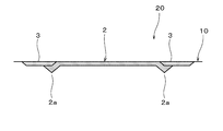
- FIG. 1 is a cross-sectional view showing a configuration of a ceramic multilayer substrate 20 according to an embodiment of the present invention
- FIG. 2 is a diagram schematically showing an enlarged main part of the ceramic multilayer substrate 20 of FIG.
- the ceramic multilayer substrate 20 includes a ceramic laminate (substrate body) 10 having a plurality of laminated ceramic layers 1 and a surface electrode (in this embodiment, Ag as a main component) formed on the surface of the ceramic laminate 10.
- a surface electrode in this embodiment, Ag as a main component
- Ag electrode 2 a coated ceramic layer 3 covering the peripheral edge 2 a of the surface electrode 2
- an internal conductor 4 such as an internal wiring 4 a and a via-hole conductor 4 b disposed inside the ceramic laminate 10. I have.
- the peripheral part 2a of the surface electrode 2 has the recessed part 12 which circulates around the surface electrode 2, the peripheral edge part (tip part) 2t of the surface electrode 2, and the surface A peripheral edge portion 2a including a region 2b in which a concave portion 12 surrounding the electrode 2 is formed is covered with a coated ceramic layer 3, and a groove 13 is also formed in the coated ceramic layer 3 in a region corresponding to the concave portion 12. ing.
- Ni plating film and an Au plating film covering the Ni plating film are formed on the surface of the central portion (exposed portion) 2c of the surface electrode 2.
- illustration of the Ni plating film and the Au plating film is omitted.
- the peripheral portion 2a of the surface electrode 2 is provided with a recess 12 that circulates the surface electrode 2, and the peripheral end (tip portion) 2t and the recess of the surface electrode 2 are provided. Since the peripheral edge portion 2a including the region 2b where 12 is formed is covered with the coating ceramic layer 3, the plating solution adhering in the plating step is blocked by the coating ceramic layer 3, and the peripheral edge portion 2a ( In particular, it becomes difficult to reach the peripheral end portion (tip portion 2t) of the surface electrode 2.
- the intruding plating solution is provided in the peripheral portion 2 a of the surface electrode 2 because the recess 12 around the surface electrode 2 is provided.
- a highly reliable ceramic multilayer substrate 20 provided with the surface electrode 2 having a sufficient peel strength is obtained.
- an electrode paste for forming a surface electrode (Ag paste in this embodiment) is applied to a ceramic green sheet 1a that becomes the ceramic layer 1 (FIGS. 1 and 2) after firing.
- An electrode paste pattern 2d is formed, and the ceramic paste pattern is coated with a ceramic paste that becomes the coated ceramic layer 3 (FIGS. 1 and 2) after firing so as to cover the peripheral portion of the electrode paste pattern 2d and expose the central portion.
- 3a is formed.
- the ceramic paste pattern 3a is disposed so as to cover a region from the outside of the peripheral end portion of the electrode paste pattern 2d to the inside of 100 ⁇ m of the peripheral end portion of the electrode paste pattern 2d.
- the resin paste that burns and decomposes and disappears in the firing process in a region retreated by 50 ⁇ m from the peripheral edge of the electrode paste pattern 2 d on the ceramic paste pattern 3 a with a width (W) of 30 ⁇ m.
- the resin paste pattern 6 is formed by applying the pattern 2d so as to circulate.
- the ceramic green sheets 1a are laminated together with other ceramic green sheets in a predetermined order so as to be the outermost layer, and then pressed to form an unfired laminated body having a flat main surface.
- the resin paste pattern 6 is provided with the ceramic paste pattern 3 a (the coated ceramic layer 3 after firing) and the electrode paste pattern 2 d (the surface electrode 2 after firing). Press.
- a recess (groove) 13a is formed in the ceramic paste pattern 3a (coated ceramic layer 3 after firing), and a recess (groove) 12a is formed in the electrode paste pattern 2d (surface electrode 2 after firing).
- the electrode paste pattern 2d (firing surface electrode 2) itself is also embedded in the ceramic green sheet 1a. For this reason, the ceramic multilayer substrate 20 after firing can be reduced in height.
- the green laminate is fired to burn and decompose the resin paste pattern.
- the recess is formed after the resin paste burns and decomposes and disappears.
- the peripheral edge 2 a of the surface electrode 2 is provided with a recess 12 that circulates the surface electrode 2, and the peripheral end (tip) 2 t and the recess of the surface electrode 2.
- the ceramic multilayer substrate 20 in which the peripheral edge portion 2a including the region 2b where 12 is formed is coated with the coated ceramic layer 3 can be obtained.
- a concave portion 13 corresponding to the concave portion 12 that circulates the surface electrode 2 is also formed in the coated ceramic layer 3, but the concave portion 13 may not be formed in the coated ceramic layer 3. .
- the recess 12 can also be formed by a method of embossing the electrode paste pattern 2d after application and drying. After embossing, a ceramic multilayer substrate having a structure in which no recess is formed in the coated ceramic layer can be obtained by applying a ceramic paste.
- the recess may be formed by embossing after forming the electrode paste pattern and the ceramic paste pattern. Is possible.
- the electrode paste pattern is entirely embedded in the ceramic green sheet in the crimping step, but not all may be embedded. In that case, the exposed portion of the surface electrode is higher than the main surface of the laminate, but the basic effect of the present invention can be obtained.
- FIG. 5 is a diagram showing a main configuration of the ceramic multilayer substrate 20 according to the second embodiment of the present invention.
- a recess 12 that circulates the surface electrode 2 is formed in the peripheral edge 2 a of the surface electrode 2, and a peripheral end (tip) 2 t and a recess 12 of the surface electrode 2 are formed.
- the region 2b in which is formed is covered with a covering ceramic layer 3 having a stepped portion.
- the altitude of the central part (exposed part) 2c not covered with the covering ceramic layer 3 of the surface electrode 2 is the ceramic laminated body in which the surface electrode 2 is formed ( Substrate main body) 10 is configured to be lower than the altitude of main surface 10a.
- the altitude is a distance from the other main surface facing the main surface 10a of the ceramic laminate (substrate body) 10 to each surface.
- the surface is a surface of the ceramic laminate (substrate body) 10 on the main surface 10a side.
- the altitude of the central portion (exposed portion) 2 c that is not covered with the coated ceramic layer 3 of the surface electrode 2 is the central portion (exposed portion) of the surface electrode 2 from the other main surface of the ceramic laminate (substrate body) 10. It is the distance to the surface of 2c.
- the elevation of the main surface 10a of the ceramic laminate (substrate body) 10 on which the surface electrode 2 is formed is the main elevation of the ceramic laminate (substrate body) 10 from the other main surface of the ceramic laminate (substrate body) 10. This is the distance to the surface 10a.
- the configuration of the other parts of the ceramic multilayer substrate 20 of the second embodiment is the same as that of the ceramic multilayer substrate of the first embodiment.
- the plating solution adhering in the plating step is blocked by the coating ceramic layer 3 and the peripheral end portion (tip end) of the surface electrode 2 Part) is difficult to reach 2t, and the plating solution adhering in the plating step accumulates in the central part 2c of the surface electrode 2 having an altitude lower than that of the main surface 10a of the ceramic laminate (substrate body) 10. It is difficult to reach the peripheral end portion (tip portion) 2t of 2. Therefore, the surface electrode 2 having sufficient peel strength can be formed even after the plating process. In addition, since the central portion 2c of the surface electrode 2 is lower than the main surface 10a, the height after mounting the component can be reduced when the component using the ceramic multilayer substrate 20 is bump-connected. .
- the ceramic multilayer substrate of Example 2 can be manufactured by the following method, for example, according to the case of manufacturing the ceramic multilayer substrate of Example 1 described above.
- (1) As shown in FIG. 6, an electrode paste for forming a surface electrode is applied to a ceramic green sheet 1a to form an electrode paste pattern 2d. The peripheral portion of the electrode paste pattern 2d is covered and the central portion is exposed.
- a ceramic paste pattern 3a is formed by applying a ceramic paste that becomes a coated ceramic layer after firing.
- the ceramic paste pattern 3a is disposed so as to cover a region from the peripheral edge of the electrode paste pattern 2d to the inside of 100 ⁇ m.
- the ceramic green sheets 1a are laminated together with other ceramic green sheets in a predetermined order so as to be the outermost layer, and then pressed to form an unfired laminated body having a flat main surface.
- the resin paste pattern 6 has a ceramic paste pattern 3 a (fired coated ceramic layer 3) and an electrode paste pattern 2 d (fired surface electrode 2) located thereunder. Press.
- a recess (groove) 13a is formed in the ceramic paste pattern 3a (coated ceramic layer 3 after firing), and a recess (groove) 12a is formed in the electrode paste pattern 2d (surface electrode 2 after firing).
- the green laminate is fired to burn and decompose the resin paste pattern.
- the recess is formed after the resin paste burns and decomposes and disappears.
- the peripheral part 2a of the surface electrode 2 is provided with the concave part 12 that goes around the surface electrode 2, and the peripheral end part (tip part) 2t and the concave part 12 of the surface electrode 2 are formed.
- the laminated layer 2b is covered with a coated ceramic layer, and the elevation of the central portion (exposed portion) 2c of the surface electrode 2 that is not covered with the coated ceramic layer 3 is such that the surface electrode 2 is formed.
- the ceramic multilayer substrate 20 configured to be lower than the altitude of the main surface 10a of the (substrate body) 10 can be obtained.
- the recessed part 12 there is no special restriction
- the ceramic multilayer substrate 20 of the second embodiment for example, as shown in FIG. 8, there is a configuration in which the width of the recess (groove) formed in the surface electrode 2 is narrow.
- the ceramic multilayer substrate 20 according to this modification can be formed by slightly shifting the area where the coated ceramic layer 3 covers the surface electrode 2, that is, by slightly increasing the area of the central portion (exposed portion) 2c. Even in the ceramic multilayer substrate configured as in this modification, the same effect as in the second embodiment can be obtained.
- FIG. 9 is a diagram showing a main part of a ceramic multilayer substrate according to another embodiment (Example 3) of the present invention.
- a recess 12 that circulates the surface electrode 2 is formed in a region that recedes inward from the peripheral end (tip portion) 2 t of the surface electrode 2.
- the ceramic multilayer substrate 20 of Example 3 is not provided with a coating ceramic layer that covers the peripheral edge of the surface electrode.
- the configuration of the other parts of the ceramic multilayer substrate 20 of the third embodiment is the same as that of the ceramic multilayer substrate of the first embodiment.
- the recess 12 that circulates the surface electrode 2 is provided in the region retracted inward from the peripheral end (tip portion) 2t of the surface electrode 2, in the plating step Even when the plating solution adheres, the plating solution accumulates in the recesses (grooves) 12 provided in the region retracted inward from the peripheral end portion (tip portion) 2t of the surface electrode 2.
- the peripheral edge portion (tip portion) 2t of the surface electrode 2 that is likely to become rust is suppressed from being corroded by the plating solution, and is highly reliable with the surface electrode 2 having sufficient peel strength even after the plating process.
- a ceramic multilayer substrate can be provided.
- the peripheral end (tip portion) 2t of the surface electrode 2 is thin and the plating tends to be insufficient, if the plating solution remains, the peripheral end (tip portion) 2t of the surface electrode 2 is plated.
- the interface between the ceramic layer 1 and the surface electrode 2 is eroded by the liquid and becomes a starting point of electrode destruction, but the region receding from the peripheral end 2a of the surface electrode 2 where the recess 12 is formed Even if the film thickness of the electrode 2 is thicker than the peripheral edge portion 2a and the plating solution is accumulated in the recess 12, the influence on the decrease in the peeling strength due to the erosion of the surface electrode 2 is within an allowable range, and the peeling of the surface electrode 2 Strength can be secured.
- the ceramic multilayer substrate 20 of Example 3 can be manufactured, for example, by the following method. (1) First, as shown in FIG. 10, an electrode paste pattern 2d is formed by applying an electrode paste for forming a surface electrode to the ceramic green sheet 1a.
- the resin paste that burns and decomposes and disappears in the firing process in a region 50 ⁇ m backward from the peripheral edge of the electrode paste pattern 2 d on the ceramic paste pattern 3 a with a width (W) of 50 ⁇ m.
- the resin paste pattern 6 is formed by applying the pattern 2d so as to circulate.
- the ceramic green sheets 1a are laminated together with other ceramic green sheets in a predetermined order so as to be the outermost layer, and then pressed to form an unfired laminated body having a flat main surface.
- this crimping step as shown in FIG. 11, as a result of the resin paste pattern 6 pressing the electrode paste pattern 2d (firing surface electrode 2) located thereunder, the electrode paste pattern 2d (firing surface after firing) A recess (groove) 12a is formed in the electrode 2).
- the electrode paste pattern 2d (firing surface electrode 2) itself is also embedded in the ceramic green sheet 1a. For this reason, the ceramic multilayer substrate 20 after firing can be reduced in height.
- the green laminate is fired to burn and decompose the resin paste pattern.
- the recess is formed after the resin paste burns and decomposes and disappears.
- the electrode paste pattern is entirely embedded in the ceramic green sheet in the crimping step. However, not all of the electrode paste pattern may be embedded. In that case, a part of the surface electrode becomes higher than the main surface of the laminate, but the basic effect of the present invention can be obtained.
- FIG. 12 is a diagram showing a main part of a ceramic multilayer substrate according to another embodiment (Example 4) of the present invention.
- the elevation of the peripheral edge 2a of the surface electrode 2 is configured to be higher than the elevation of the central portion (exposed portion) 2c of the surface electrode 2.
- the ceramic multilayer substrate 20 of Example 4 is not provided with a coating ceramic layer that covers the peripheral portion of the surface electrode.
- the configuration of the other parts of the ceramic multilayer substrate 20 of the fourth embodiment is the same as that of the ceramic multilayer substrate of the first embodiment.
- the elevation of the peripheral portion 2a of the surface electrode 2 is made higher than the elevation of the central portion 2c of the surface electrode 2, and the central portion 2c has an elevation higher than that of the peripheral portion 2a. Since it is configured to be low, even if the plating solution remains after the plating step, the plating solution is accumulated in the central portion 2c inside the peripheral portion 2a, so that sufficient peel strength is obtained even after the plating step. It is possible to provide a highly reliable ceramic multilayer substrate 20 including the surface electrode 2 having the following.
- the ceramic multilayer substrate 20 of Example 4 can be manufactured by the following method, for example. (1) First, as shown in FIG. 13, an electrode paste pattern 2d is formed by applying an electrode paste for forming a surface electrode to the ceramic green sheet 1a.
- the ceramic green sheets 1a are laminated together with other ceramic green sheets in a predetermined order so as to be the outermost layer, and then pressed to form an unfired laminated body having a flat main surface.
- the resin paste pattern 6 presses the electrode paste pattern 2d (firing surface electrode 2) positioned therebelow, as a result of which the electrode paste pattern 2d ( The whole center part except the peripheral part of the surface electrode 2) after baking becomes a recessed shape.
- the electrode paste pattern 2d (surface electrode 2 after firing) itself is also embedded in the ceramic green sheet. For this reason, the ceramic multilayer substrate 20 after firing can be reduced in height.
- the green laminate is fired to burn and decompose the resin paste pattern.
- the recess is formed after the resin paste burns and decomposes and disappears.
- the ceramic multilayer substrate 20 including the surface electrode 2 having a structure in which the elevation of the peripheral edge portion 2a of the surface electrode 2 is higher than the elevation of the central portion (exposed portion) 2c of the surface electrode 2 is provided. Is obtained.
- the electrode paste pattern is entirely embedded in the ceramic green sheet in the crimping step. However, not all of the electrode paste pattern may be embedded. In that case, a part of the surface electrode (for example, the peripheral portion) becomes higher than the main surface of the laminate, but the basic effect of the present invention can be obtained.
- the peel strength of the surface electrode was examined for the ceramic multilayer substrate produced in each of the above examples.
- a 2 mm square surface electrode was formed, and the peel strength of this surface electrode was measured.
- 2 mm square is a square having a side of 2 mm.
- a ceramic multilayer substrate 20 in which a surface electrode 2 having a structure in which a peripheral edge 2a is covered with a covering ceramic layer 3 is provided on the surface of a ceramic laminate (substrate body) 10 as shown in FIG. (Comparative Example 1)
- the peel strength (N / 2mm ⁇ ) of the surface electrode was examined. The peel strength is obtained by measuring the peel strength of the surface electrode when a predetermined copper wire is soldered to the surface electrode and the copper wire is pulled in a direction perpendicular to the surface electrode. The results are shown in Table 1.
- each sample of Table 1 is as follows.
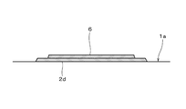
- Comparative example (conventional example) 1 FIG. 16 shows a ceramic multilayer substrate provided with a surface electrode whose peripheral edge is covered with a coating ceramic layer.
- Comparative example (conventional example) 2 FIG. 17 shows a ceramic multilayer substrate provided with a surface electrode not coated with a coated ceramic layer.
- Sample 1 of Example Ceramic multilayer substrate provided with the surface electrode of FIGS. 1 and 2 manufactured in Example 1 (4) Sample 2-1 of Example Ceramic multilayer substrate provided with the surface electrode of FIG. 5 produced in Example 2 (5)
- Sample 3 of Example The ceramic multilayer substrate provided with the surface electrode of FIG. 9 produced in Example 3 (7) Sample 4 of Example The ceramic multilayer substrate provided with the surface electrode of FIG.
- the peel strength of the surface electrode was insufficient at 22 N / 2 mm ⁇ and 20 N / 2 mm ⁇ . However, it was confirmed that the peel strength of the surface electrode was significantly improved to 27 to 34 N / 2 mm ⁇ in the ceramic multilayer substrate produced in Examples 1 to 4 and satisfying the requirements of the present invention. .
- the present invention is not limited to each of the above-described embodiments.
- the constituent material of the surface electrode, the specific shape, the number and arrangement of the arrangement, the arrangement when the coating ceramic layer is provided, the coating ceramic Within the scope of the invention, there are various compositions relating to the specific composition of the ceramic constituting the layer, the number of laminated ceramic layers constituting the ceramic substrate, the arrangement of internal conductors, the specific composition of the ceramic constituting the ceramic substrate, etc. It is possible to add applications and modifications.
- the peripheral portion 2a of the surface electrode 2 is formed with a recess 12 that circulates the surface electrode 2, and when viewed from the top in the stacking direction of the ceramic multilayer substrate 20, FIG. As shown in (a).
- the surface electrode having sufficient peel strength not only when the recess is formed so as to circulate around the surface electrode but also when the recess is formed at a part of the peripheral edge of the surface electrode. Can be formed.
- the surface electrode 2 having sufficient peel strength can be formed by forming the recesses 12 at the peripheral edges of the two opposite sides of the surface electrode 2.
Abstract
めっき工程を経た後においても、十分な剥離強度を有する表面電極を備えた信頼性の高いセラミック多層基板を提供する。 積層された複数のセラミック層を備えてなるセラミック積層体と、セラミック積層体の表面に形成された表面電極と、表面電極の周縁部を被覆する被覆セラミック層を備えてなるセラミック多層基板において、表面電極2の周縁部2aに、表面電極を周回する凹部12が形成されているとともに、表面電極の、周端部および凹部が形成された領域を含む周縁部が被覆セラミック層3により被覆された構成とする。 また、表面電極の被覆セラミック層により被覆されていない中央部の標高が、表面電極が形成されたセラミック積層体の主面の標高よりも低い構成とする。
Description
本発明はセラミック多層基板に関し、詳しくは、積層された複数のセラミック層を備えてなるセラミック積層体の表面に表面電極が形成されたセラミック多層基板に関する。
セラミック多層基板は、通常、複数のセラミック層が積層されたセラミック基板(基板本体)の表面および内部に、表面電極や内部導体を備えた構造を有している。
このようなセラミック多層基板においては、実装信頼性を確保するため、表面電極が実用上問題のない剥離強度を備えていることが必要になる。
ところで、セラミック多層基板の表面に配設された表面電極の剥離強度が低下する要因の一つに、表面電極の表面にめっき膜を形成するためのめっき工程で用いられるめっき液の影響が挙げられる。
これは、めっき液がセラミック多層基板の表面に残留して、セラミック多層基板を構成するセラミックと表面電極との界面の脆弱化をもたらすことによる。
これは、めっき液がセラミック多層基板の表面に残留して、セラミック多層基板を構成するセラミックと表面電極との界面の脆弱化をもたらすことによる。
また、表面電極は、その周端部(先端部)を起点として剥離が起こり易くなっているため、表面電極の周端部(先端部)にめっき液の残留があった場合には、剥離強度に対する影響は顕著となる。
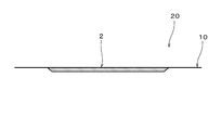
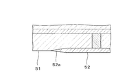
例えば、図18に示すように、表面電極52の周端部(先端部)を含めた主要部がセラミック多層基板を構成する最外層のセラミック層51の表面に形成されている場合(特許文献1の図11参照)、表面電極52の周端部(先端部)52aがセラミック層51との境界に位置しており、この位置は、めっき液が残留しやすい部分であることから、表面電極の剥離強度の低下を招きやすい。
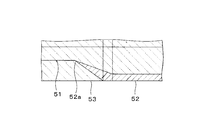
また、図19に示すように、表面電極52の周端部(先端部)52aが被覆セラミック層53により被覆された構成の場合(特許文献1の図2参照)も、セラミック層51と表面電極52の境界部53からめっき液が浸入する場合があり、その場合にはめっき液が、被覆セラミック層53により被覆された表面電極52の周端部(先端部)にまで浸透して残留し、剥離強度の低下を招くという問題点がある。
また、めっき液が残留した状態で、セラミック多層基板を乾燥の工程に供した場合、常温よりも高い乾燥温度にさらされることになる。そのような場合、例えば、めっき膜としてNiめっき膜(下層)とAuめっき(上層)が形成されている場合、Niの、Auめっき膜への拡散が生じる。これはNiがAuよりもイオン化傾向が高く、Auと置換しやすいためである。そして、このNiの拡散は、しみや変色の原因となり、外観不良を引き起こすおそれがある。また、めっき膜がNiめっき膜(下層)、Snめっき膜(上層)である場合には、乾燥温度が高くなると、Snが酸化したり、溶解したりするという問題点がある。
本発明は、上記課題を解決するものであり、めっき工程を経た後においても、十分な剥離強度を有する表面電極を備えた信頼性の高いセラミック多層基板を提供することを目的とする。
上記課題を解決するために、本発明のセラミック多層基板は、
積層された複数のセラミック層を備えてなるセラミック積層体と、前記セラミック積層体の表面に形成された表面電極とを備えてなるセラミック多層基板であって、
前記表面電極の周端部より内側に後退した領域に、凹部が形成されていること
を特徴としている。
積層された複数のセラミック層を備えてなるセラミック積層体と、前記セラミック積層体の表面に形成された表面電極とを備えてなるセラミック多層基板であって、
前記表面電極の周端部より内側に後退した領域に、凹部が形成されていること
を特徴としている。
この構成を備えることにより、めっき工程でめっき液が付着した場合にも、めっき液は表面電極の周端部より内側に後退した領域に設けられた凹部(溝)に溜まるため、電極破壊や電極剥離の起点となりやすい表面電極の周端部のめっき液による腐食が抑制され、めっき工程を経た後においても、十分な剥離強度を有する表面電極を備えた信頼性の高いセラミック多層基板を提供することが可能になる。すなわち、本発明によれば、表面電極の周端部(先端部)は厚みが薄く、めっきの付きも不十分になりやすいため、そこにめっき液が残留すると、表面電極の周端部がめっき液により浸食されてセラミックと表面電極の界面がもろくなり、電極破壊の起点となるが、本発明においては、めっき液が表面電極の周端部より内側に後退した領域に設けられた凹部(溝)に溜まるため、表面電極の周端部がめっき液により浸食されることを抑制、防止して、めっき工程を経た後においても表面電極の剥離強度を高く保持することができる。なお、凹部が形成される表面電極の周端部より内側に後退した領域は、表面電極の膜厚が周縁部よりも厚く、めっき液が凹部に溜まったとしても、表面電極が浸食されることによる剥離強度の低下についての影響は許容範囲となり、表面電極の剥離強度を確保することができる。
また、本発明のセラミック多層基板において、前記凹部は、前記表面電極を周回するように形成されていることが好ましい。
この構成を備えることにより、より表面電極の剥離強度を高く保持することができる。
この構成を備えることにより、より表面電極の剥離強度を高く保持することができる。
また、本発明のセラミック多層基板は、
積層された複数のセラミック層を備えてなるセラミック積層体と、前記セラミック積層体の表面に形成された表面電極とを備えてなるセラミック多層基板であって、
前記表面電極の周縁部の標高が、前記表面電極の中央部の標高よりも高くなるように構成されていること
を特徴としている。
積層された複数のセラミック層を備えてなるセラミック積層体と、前記セラミック積層体の表面に形成された表面電極とを備えてなるセラミック多層基板であって、
前記表面電極の周縁部の標高が、前記表面電極の中央部の標高よりも高くなるように構成されていること
を特徴としている。
この構成を備えることにより、めっき工程後にめっき液が残留したとしても、周端部(先端部)を含む周縁部よりも内側の領域にめっき液が溜まるため、上述の場合と同様に、めっき工程を経た後においても、十分な剥離強度を有する表面電極を備えた信頼性の高いセラミック多層基板を提供することが可能になる。
また、本発明のセラミック多層基板は、
積層された複数のセラミック層を備えてなるセラミック積層体と、前記セラミック積層体の表面に形成された表面電極と、前記表面電極の周縁部を被覆する被覆セラミック層を備えてなるセラミック多層基板であって、
前記表面電極の周縁部に、凹部が形成されているとともに、前記表面電極の、周端部および前記凹部が形成された領域を含む前記周縁部が前記被覆セラミック層により被覆されていること
を特徴としている。
積層された複数のセラミック層を備えてなるセラミック積層体と、前記セラミック積層体の表面に形成された表面電極と、前記表面電極の周縁部を被覆する被覆セラミック層を備えてなるセラミック多層基板であって、
前記表面電極の周縁部に、凹部が形成されているとともに、前記表面電極の、周端部および前記凹部が形成された領域を含む前記周縁部が前記被覆セラミック層により被覆されていること
を特徴としている。
この構成を備えることにより、めっき工程で付着しためっき液は、被覆セラミック層により遮られて、表面電極の周縁部にまで達しにくくなる。また、被覆セラミック層と表面電極の界面からめっき液が侵入した場合も、表面電極の周端部から後退した位置に凹部が形成されているため、侵入しためっき液が凹部に溜まり、表面電極の周端部にまで達しにくく、めっき工程を経た後においても、十分な剥離強度を有する表面電極を備えた信頼性の高いセラミック多層基板を提供することが可能になる。
また、本発明のセラミック多層基板において、前記凹部は、前記表面電極を周回するように形成されていることが好ましい。
この構成を備えることにより、表面電極の剥離強度を高く保持することができる。
この構成を備えることにより、表面電極の剥離強度を高く保持することができる。
また、本発明のセラミック多層基板においては、前記表面電極の前記被覆セラミック層により被覆されていない中央部の標高が、前記表面電極が形成された前記セラミック積層体の主面の標高よりも低いことが好ましい。
この構成を備えることにより、めっき工程で付着しためっき液は、被覆セラミック層により遮られて、表面電極の周端部(先端部)を含む周縁部にまで達しにくくなり、また、めっき工程で付着しためっき液は、セラミック積層体の主面よりも標高の低い、表面電極の中央領域に溜まるため、めっき工程を経た後においても十分な剥離強度を有する表面電極を備えた信頼性の高いセラミック多層基板を提供することが可能になる。
また、本発明のセラミック多層基板においては、前記表面電極の表面の少なくとも一部は、前記セラミック積層体の表面に埋設されていることが好ましい。
なお、表面電極の少なくとも一部がセラミック積層体の表面に埋設されているとは、表面電極の少なくとも一部がセラミック積層体の表面に埋没していることを意味するものであり、例えば、
・表面電極が所定の露出部分を残してセラミック積層体に埋没し、前記露出部分がセラミック積層体の表面と同一平面にある(標高が同じである)場合、
・表面電極が所定の露出部分を残してセラミック積層体に埋没し、前記露出部分の標高が、セラミック積層体の標高よりも低い場合、
・表面電極の一部がセラミック積層体に埋没し、表面電極の前記露出部分の標高が、セラミック積層体の標高よりもいくらか高いような場合
などを含む概念である。
なお、表面電極の少なくとも一部がセラミック積層体の表面に埋設されているとは、表面電極の少なくとも一部がセラミック積層体の表面に埋没していることを意味するものであり、例えば、
・表面電極が所定の露出部分を残してセラミック積層体に埋没し、前記露出部分がセラミック積層体の表面と同一平面にある(標高が同じである)場合、
・表面電極が所定の露出部分を残してセラミック積層体に埋没し、前記露出部分の標高が、セラミック積層体の標高よりも低い場合、
・表面電極の一部がセラミック積層体に埋没し、表面電極の前記露出部分の標高が、セラミック積層体の標高よりもいくらか高いような場合
などを含む概念である。
この構成を備えることにより、表面電極がセラミック積層体の表面から突出しないようにしたり、表面電極の上面のセラミック積層体表面からの突出量(距離)を減らしたりすることが可能になり、セラミック多層基板の低背化に寄与することができる。
また、前記表面電極の表面の少なくとも一部には、めっき膜が形成されていることが好ましい。
この構成を備えることにより、めっき液による表面強度の剥離強度を高く保持することができる。
この構成を備えることにより、めっき液による表面強度の剥離強度を高く保持することができる。
本発明のセラミック多層基板は、めっき工程でめっき液が付着した場合にも、電極破壊や電極剥離の起点となりやすい表面電極の周端部のめっき液による腐食が抑制され、めっき工程を経た後においても、十分な剥離強度を有する表面電極を備えた信頼性の高いセラミック多層基板を提供することが可能になる。
以下に本発明の実施例を示して、本発明の特徴とするところをさらに詳しく説明する。
[セラミック多層基板の構成]
図1は、本発明の実施例にかかるセラミック多層基板20の構成を示す断面図、図2は図1のセラミック多層基板20の要部を拡大して模式的に示す図である。
図1は、本発明の実施例にかかるセラミック多層基板20の構成を示す断面図、図2は図1のセラミック多層基板20の要部を拡大して模式的に示す図である。
このセラミック多層基板20は、積層された複数のセラミック層1を備えてなるセラミック積層体(基板本体)10と、セラミック積層体10の表面に形成された表面電極(この実施例ではAgを主成分とするAg電極)2と、表面電極2の周縁部2aを被覆する被覆セラミック層3と、セラミック積層体10の内部に配設された、内部配線4aやビアホール導体4bなどの内部導体4とを備えている。
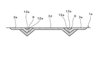
そして、図2に示すように、表面電極2の周縁部2aには、表面電極2を周回する凹部12が形成されているとともに、表面電極2の、周端部(先端部)2t、および表面電極2を周回する凹部12が形成された領域2bを含む周縁部2aが、被覆セラミック層3により被覆されており、被覆セラミック層3にも、上記凹部12に対応する領域に溝13が形成されている。
また、表面電極2の中央部(露出部)2cの表面には、Niめっき膜、およびNiめっき膜を覆うAuめっき膜が形成されている。なお、図1,図2においては、Niめっき膜およびAuめっき膜の図示を省略している。
この実施例1のセラミック多層基板20においては、表面電極2の周縁部2aに、表面電極2を周回する凹部12が設けられ、かつ、表面電極2の、周端部(先端部)2tおよび凹部12が形成された領域2bを含む周縁部2aが被覆セラミック層3により被覆されているので、めっき工程で付着しためっき液は、被覆セラミック層3により遮られて、表面電極2の周縁部2a(特に表面電極2の周端部(先端部)2t)にまで達しにくくなる。また、被覆セラミック層3と表面電極2の界面からめっき液が侵入した場合にも、表面電極2の周縁部2aに、表面電極2を周回する凹部12が設けられているため、侵入しためっき液が表面電極2の周縁部2a(特に表面電極の周端部(先端部)2t)にまで達しにくくなる。その結果、めっき工程を経た後においても、十分な剥離強度を有する表面電極2を備えた信頼性の高いセラミック多層基板20が得られる。
[セラミック多層基板の製造方法]
次に、上述のセラミック多層基板20の製造方法について説明する。
(1)まず、図3に示すように、焼成後にセラミック層1(図1,2)となるセラミックグリーンシート1aに、表面電極形成用の電極ペースト(この実施例ではAgペースト)を塗布して電極ペーストパターン2dを形成し、この電極ペーストパターン2dの周縁部を覆い、中央部を露出させるように、焼成後に被覆セラミック層3(図1,2)となるセラミックペーストを塗布してセラミックペーストパターン3aを形成する。セラミックペーストパターン3aは、電極ペーストパターン2dの周端部より外側から、電極ペーストパターン2dの周端部の100μm内側までの領域を覆うように配設する。
(2)それから、セラミックペーストパターン3a上の、電極ペーストパターン2dの周端部から50μm後退した領域に、焼成工程で燃焼、分解して消失する樹脂ペーストを、幅(W)30μmで、電極ペーストパターン2dを周回するように塗布して樹脂ペーストパターン6を形成する。
(3)そして、このセラミックグリーンシート1aが最外層となるように他のセラミックグリーンシートとともに所定の順序で積層した後、圧着して、主面が平坦な未焼成積層体を形成する。
この圧着の工程で、図4に示すように、樹脂ペーストパターン6が、その下に位置するセラミックペーストパターン3a(焼成後の被覆セラミック層3)および電極ペーストパターン2d(焼成後の表面電極2)を押圧する。その結果、セラミックペーストパターン3a(焼成後の被覆セラミック層3)には凹部(溝)13aが形成され、電極ペーストパターン2d(焼成後の表面電極2)には凹部(溝)12aが形成される。また、電極ペーストパターン2d(焼成後の表面電極2)自体もセラミックグリーンシート1aに埋設される。このため焼成後のセラミック多層基板20の低背化を図ることができる。
この圧着の工程で、図4に示すように、樹脂ペーストパターン6が、その下に位置するセラミックペーストパターン3a(焼成後の被覆セラミック層3)および電極ペーストパターン2d(焼成後の表面電極2)を押圧する。その結果、セラミックペーストパターン3a(焼成後の被覆セラミック層3)には凹部(溝)13aが形成され、電極ペーストパターン2d(焼成後の表面電極2)には凹部(溝)12aが形成される。また、電極ペーストパターン2d(焼成後の表面電極2)自体もセラミックグリーンシート1aに埋設される。このため焼成後のセラミック多層基板20の低背化を図ることができる。
(4)それから、この未焼成積層体を焼成し、樹脂ペーストパターンを燃焼、分解させる。その結果、樹脂ペーストが燃焼、分解して消失した後に凹部が形成される。
これにより、図1,2に示すように、表面電極2の周縁部2aに、表面電極2を周回する凹部12が設けられ、かつ、表面電極2の、周端部(先端部)2tおよび凹部12が形成された領域2bを含む周縁部2aが被覆セラミック層3により被覆されたセラミック多層基板20を得ることができる。
この方法の場合、被覆セラミック層3にも、表面電極2を周回する凹部12に対応する凹部13が形成されることになるが、被覆セラミック層3には凹部13は形成されていなくてもよい。
なお、凹部12は、塗布、乾燥後の電極ペーストパターン2dを型押しする方法によっても形成することができる。型押しした後、セラミックペーストを塗布することにより、被覆セラミック層には凹部が形成されていない構造のセラミック多層基板を得ることができる。
本発明においては、凹部を形成する方法に特別の制約はなく、上述の方法の他にも、電極ペーストパターンと、セラミックペーストパターンとを形成した後、型押しすることにより凹部を形成することも可能である。
また、上記製造方法の例では、圧着の工程で、電極ペーストパターンが全てセラミックグリーンシートに埋設されるようにしているが、全てが埋設されなくてもよい。その場合には表面電極の露出部などは積層体の主面よりも高くなるが、本発明の基本的な効果を得ることは可能である。
本発明においては、凹部を形成する方法に特別の制約はなく、上述の方法の他にも、電極ペーストパターンと、セラミックペーストパターンとを形成した後、型押しすることにより凹部を形成することも可能である。
また、上記製造方法の例では、圧着の工程で、電極ペーストパターンが全てセラミックグリーンシートに埋設されるようにしているが、全てが埋設されなくてもよい。その場合には表面電極の露出部などは積層体の主面よりも高くなるが、本発明の基本的な効果を得ることは可能である。
[セラミック多層基板の構成]
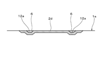
図5は、本発明の実施例2にかかるセラミック多層基板20の要部構成を示す図である。
この実施例2のセラミック多層基板においては、表面電極2の周縁部2aに、表面電極2を周回する凹部12が形成されているとともに、表面電極2の周端部(先端部)2tおよび凹部12が形成された領域2bが、段部を有する被覆セラミック層3により被覆されている。
図5は、本発明の実施例2にかかるセラミック多層基板20の要部構成を示す図である。
この実施例2のセラミック多層基板においては、表面電極2の周縁部2aに、表面電極2を周回する凹部12が形成されているとともに、表面電極2の周端部(先端部)2tおよび凹部12が形成された領域2bが、段部を有する被覆セラミック層3により被覆されている。
そして、この実施例2のセラミック多層基板20においては、表面電極2の被覆セラミック層3により被覆されていない中央部(露出部)2cの標高が、表面電極2が形成されているセラミック積層体(基板本体)10の主面10aの標高よりも低くなるように構成されている。
ここで標高とは、セラミック積層体(基板本体)10の主面10aと対向する他方主面から、それぞれの表面までの距離である。表面とはセラミック積層体(基板本体)10の主面10a側の面である。つまり、表面電極2の被覆セラミック層3により被覆されていない中央部(露出部)2cの標高とは、セラミック積層体(基板本体)10の他方主面から表面電極2の中央部(露出部)2cの表面までの距離である。また、表面電極2が形成されているセラミック積層体(基板本体)10の主面10aの標高とは、セラミック積層体(基板本体)10の他方主面からセラミック積層体(基板本体)10の主面10aまでの距離である。
ここで標高とは、セラミック積層体(基板本体)10の主面10aと対向する他方主面から、それぞれの表面までの距離である。表面とはセラミック積層体(基板本体)10の主面10a側の面である。つまり、表面電極2の被覆セラミック層3により被覆されていない中央部(露出部)2cの標高とは、セラミック積層体(基板本体)10の他方主面から表面電極2の中央部(露出部)2cの表面までの距離である。また、表面電極2が形成されているセラミック積層体(基板本体)10の主面10aの標高とは、セラミック積層体(基板本体)10の他方主面からセラミック積層体(基板本体)10の主面10aまでの距離である。
なお、特に図示していないが、この実施例2のセラミック多層基板20の他の部分の構成は、上記実施例1のセラミック多層基板と同様である。
このセラミック多層基板20の場合も、上記実施例1のセラミック多層基板20の場合と同じく、めっき工程で付着しためっき液は、被覆セラミック層3により遮られて、表面電極2の周端部(先端部)2tにまで達しにくく、また、めっき工程で付着しためっき液は、セラミック積層体(基板本体)10の主面10aよりも標高の低い、表面電極2の中央部2cに溜まるため、表面電極2の周端部(先端部)2tにまで達しにくい。したがって、めっき工程を経た後においても、十分な剥離強度を有する表面電極2を形成することができる。
また、表面電極2の中央部2cが主面10aよりも低くなっているため、セラミック多層基板20を用いた部品をバンプ接続する場合などに、部品の実装後の高さを低くすることができる。
また、表面電極2の中央部2cが主面10aよりも低くなっているため、セラミック多層基板20を用いた部品をバンプ接続する場合などに、部品の実装後の高さを低くすることができる。
[セラミック多層基板の製造方法]
この実施例2セラミック多層基板は、上述の実施例1のセラミック多層基板を製造する場合に準じて、例えば、以下の方法で製造することができる。
(1)図6に示すように、セラミックグリーンシート1aに、表面電極形成用の電極ペーストを塗布して電極ペーストパターン2dを形成し、この電極ペーストパターン2dの周縁部を覆い、中央部を露出させるように、焼成後に被覆セラミック層となるセラミックペーストを塗布してセラミックペーストパターン3aを形成する。
なお、セラミックペーストパターン3aは、電極ペーストパターン2dの周端部から100μm内側までの領域を覆うように配設する。
この実施例2セラミック多層基板は、上述の実施例1のセラミック多層基板を製造する場合に準じて、例えば、以下の方法で製造することができる。
(1)図6に示すように、セラミックグリーンシート1aに、表面電極形成用の電極ペーストを塗布して電極ペーストパターン2dを形成し、この電極ペーストパターン2dの周縁部を覆い、中央部を露出させるように、焼成後に被覆セラミック層となるセラミックペーストを塗布してセラミックペーストパターン3aを形成する。
なお、セラミックペーストパターン3aは、電極ペーストパターン2dの周端部から100μm内側までの領域を覆うように配設する。
(2)それから、セラミックペーストパターン3a上の、電極ペーストパターン2dの周端部(先端部)から50μm後退した位置より内側の全領域に、焼成工程で燃焼、分解して消失する樹脂ペーストを塗布して樹脂ペーストパターン6を形成する。
(3)そして、このセラミックグリーンシート1aが最外層となるように他のセラミックグリーンシートとともに所定の順序で積層した後、圧着して、主面が平坦な未焼成積層体を形成する。
この圧着の工程で、図7に示すように、樹脂ペーストパターン6が、その下に位置するセラミックペーストパターン3a(焼成後の被覆セラミック層3)および電極ペーストパターン2d(焼成後の表面電極2)を押圧する。その結果、セラミックペーストパターン3a(焼成後の被覆セラミック層3)には凹部(溝)13aが形成され、電極ペーストパターン2d(焼成後の表面電極2)には凹部(溝)12aが形成される。
この圧着の工程で、図7に示すように、樹脂ペーストパターン6が、その下に位置するセラミックペーストパターン3a(焼成後の被覆セラミック層3)および電極ペーストパターン2d(焼成後の表面電極2)を押圧する。その結果、セラミックペーストパターン3a(焼成後の被覆セラミック層3)には凹部(溝)13aが形成され、電極ペーストパターン2d(焼成後の表面電極2)には凹部(溝)12aが形成される。
(4)それから、この未焼成積層体を焼成し、樹脂ペーストパターンを燃焼、分解させる。その結果、樹脂ペーストが燃焼、分解して消失した後に凹部が形成される。
これにより、図5に示すように、表面電極2の周縁部2aに、表面電極2を周回する凹部12が設けられ、かつ、表面電極2の周端部(先端部)2tおよび凹部12が形成された領域2bが被覆セラミック層により被覆されているとともに、表面電極2の被覆セラミック層3により被覆されていない中央部(露出部)2cの標高が、表面電極2が形成されているセラミック積層体(基板本体)10の主面10aの標高よりも低くなるように構成されたセラミック多層基板20を得ることができる。
なお、凹部12の形成方法には特別の制約はなく、例えば、塗布、乾燥後の電極ペーストパターン2dを型押しする方法によっても形成することができる。
[変形例]
この実施例2のセラミック多層基板20の変形例として、例えば、図8に示すように、表面電極2に形成された凹部(溝)の幅が狭い構成のものが挙げられる。
この変形例にかかるセラミック多層基板20は、被覆セラミック層3が表面電極2を覆う領域を少しずらす、すなわち、中央部(露出部)2cの面積を少し大きくすることにより形成することができる。
この変形例のような構成のセラミック多層基板においても、上記実施例2の場合と同様の効果を得ることができる。
この実施例2のセラミック多層基板20の変形例として、例えば、図8に示すように、表面電極2に形成された凹部(溝)の幅が狭い構成のものが挙げられる。
この変形例にかかるセラミック多層基板20は、被覆セラミック層3が表面電極2を覆う領域を少しずらす、すなわち、中央部(露出部)2cの面積を少し大きくすることにより形成することができる。
この変形例のような構成のセラミック多層基板においても、上記実施例2の場合と同様の効果を得ることができる。
[セラミック多層基板の構成]
図9は、本発明の他の実施例(実施例3)の発明にかかるセラミック多層基板の要部を示す図である。
この実施例3のセラミック多層基板においては、表面電極2の周端部(先端部)2tより内側に後退した領域に、表面電極2を周回する凹部12が形成されている。
図9は、本発明の他の実施例(実施例3)の発明にかかるセラミック多層基板の要部を示す図である。
この実施例3のセラミック多層基板においては、表面電極2の周端部(先端部)2tより内側に後退した領域に、表面電極2を周回する凹部12が形成されている。
ただし、この実施例3のセラミック多層基板20では、上記実施例1および2のセラミック多層基板とは異なり、表面電極の周縁部を被覆する被覆セラミック層は設けられていない。
なお、特に図示していないが、この実施例3のセラミック多層基板20の他の部分の構成は、上記実施例1のセラミック多層基板と同様である。
この実施例3のセラミック多層基板20においては、表面電極2の周端部(先端部)2tより内側に後退した領域に、表面電極2を周回する凹部12が設けられているので、めっき工程でめっき液が付着した場合にも、めっき液は表面電極2の周端部(先端部)2tより内側に後退した領域に設けられた凹部(溝)12に溜まるため、電極破壊や電極剥離の起点となりやすい表面電極2の周端部(先端部)2tがめっき液により腐食されることが抑制され、めっき工程を経た後においても、十分な剥離強度を有する表面電極2を備えた信頼性の高いセラミック多層基板を提供することができる。
すなわち、表面電極2の周端部(先端部)2tは厚みが薄く、めっきの付きも不十分になりやすいため、めっき液が残留すると、表面電極2の周端部(先端部)2tがめっき液により浸食されてセラミック層1と表面電極2の界面がもろくなり、電極破壊の起点となりやすくなるが、凹部12が形成される表面電極2の周端部2aより内側に後退した領域は、表面電極2の膜厚が周縁部2aよりも厚く、めっき液が凹部12に溜まったとしても、表面電極2が浸食されることによる剥離強度の低下についての影響は許容範囲となり、表面電極2の剥離強度を確保することができる。
[セラミック多層基板の製造方法]
この実施例3のセラミック多層基板20は、例えば、以下の方法で製造することができる。
(1)まず、図10に示すように、このセラミックグリーンシート1aに、表面電極形成用の電極ペーストを塗布して電極ペーストパターン2dを形成する。
この実施例3のセラミック多層基板20は、例えば、以下の方法で製造することができる。
(1)まず、図10に示すように、このセラミックグリーンシート1aに、表面電極形成用の電極ペーストを塗布して電極ペーストパターン2dを形成する。
(2)それから、セラミックペーストパターン3a上の、電極ペーストパターン2dの周端部から50μm後退した領域に、焼成工程で燃焼、分解して消失する樹脂ペーストを、幅(W)50μmで、電極ペーストパターン2dを周回するように塗布して樹脂ペーストパターン6を形成する。
(3)そして、このセラミックグリーンシート1aが最外層となるように他のセラミックグリーンシートとともに所定の順序で積層した後、圧着して、主面が平坦な未焼成積層体を形成する。
この圧着の工程で、図11に示すように、樹脂ペーストパターン6が、その下に位置する電極ペーストパターン2d(焼成後の表面電極2)を押圧する結果、電極ペーストパターン2d(焼成後の表面電極2)に凹部(溝)12aが形成される。
また、電極ペーストパターン2d(焼成後の表面電極2)自体もセラミックグリーンシート1aに埋設される。このため焼成後のセラミック多層基板20の低背化を図ることができる。
この圧着の工程で、図11に示すように、樹脂ペーストパターン6が、その下に位置する電極ペーストパターン2d(焼成後の表面電極2)を押圧する結果、電極ペーストパターン2d(焼成後の表面電極2)に凹部(溝)12aが形成される。
また、電極ペーストパターン2d(焼成後の表面電極2)自体もセラミックグリーンシート1aに埋設される。このため焼成後のセラミック多層基板20の低背化を図ることができる。
(4)それから、この未焼成積層体を焼成し、樹脂ペーストパターンを燃焼、分解させる。その結果、樹脂ペーストが燃焼、分解して消失した後に凹部が形成される。
これにより、図9に示すように、表面電極2の周端部(先端部)2tより内側に後退した領域に、表面電極2を周回する凹部12が形成されたセラミック多層基板を得ることができる。
なお、上記製造方法の例では、圧着の工程で、電極ペーストパターンが全てセラミックグリーンシートに埋設されるようにしているが、全てが埋設されなくてもよい。その場合には表面電極の一部が積層体の主面よりも高くなることになるが、本発明の基本的な効果を得ることは可能である。
なお、上記製造方法の例では、圧着の工程で、電極ペーストパターンが全てセラミックグリーンシートに埋設されるようにしているが、全てが埋設されなくてもよい。その場合には表面電極の一部が積層体の主面よりも高くなることになるが、本発明の基本的な効果を得ることは可能である。
[セラミック多層基板の構成]
図12は、本発明の他の実施例(実施例4)の発明にかかるセラミック多層基板の要部を示す図である。
この実施例4のセラミック多層基板においては、表面電極2の周縁部2aの標高が、表面電極2の中央部(露出部)2cの標高よりも高くなるように構成されている。
図12は、本発明の他の実施例(実施例4)の発明にかかるセラミック多層基板の要部を示す図である。
この実施例4のセラミック多層基板においては、表面電極2の周縁部2aの標高が、表面電極2の中央部(露出部)2cの標高よりも高くなるように構成されている。
ただし、この実施例4のセラミック多層基板20では、上記実施例1および2のセラミック多層基板とは異なり、表面電極の周縁部を被覆する被覆セラミック層は設けられていない。
なお、特に図示していないが、この実施例4のセラミック多層基板20の他の部分の構成は、上記実施例1のセラミック多層基板と同様である。
この実施例4のセラミック多層基板20においては、表面電極2の周縁部2aの標高を、表面電極2の中央部2cの標高よりも高くして、中央部2cのほうが周縁部2aよりも標高が低くなるように構成しているので、めっき工程後にめっき液が残留したとしても、周縁部2aよりも内側の中央部2cにめっき液が溜まるため、めっき工程を経た後においても、十分な剥離強度を有する表面電極2を備えた信頼性の高いセラミック多層基板20を提供することが可能になる。
[セラミック多層基板の製造方法]
この実施例4のセラミック多層基板20は、例えば、以下の方法で製造することができる。
(1)まず、図13に示すように、このセラミックグリーンシート1aに、表面電極形成用の電極ペーストを塗布して電極ペーストパターン2dを形成する。
この実施例4のセラミック多層基板20は、例えば、以下の方法で製造することができる。
(1)まず、図13に示すように、このセラミックグリーンシート1aに、表面電極形成用の電極ペーストを塗布して電極ペーストパターン2dを形成する。
(2)それから、セラミックペーストパターン3a上の、電極ペーストパターン2dの周端部から50μm後退した位置より内側の全領域に、焼成工程で燃焼、分解して消失する樹脂ペーストを塗布して樹脂ペーストパターン6を形成する。
(3)そして、このセラミックグリーンシート1aが最外層となるように他のセラミックグリーンシートとともに所定の順序で積層した後、圧着して、主面が平坦な未焼成積層体を形成する。
この圧着の工程で、図14に要部構成を示すように、樹脂ペーストパターン6が、その下に位置する電極ペーストパターン2d(焼成後の表面電極2)を押圧する結果、電極ペーストパターン2d(焼成後の表面電極2)の周縁部を除いた中央部全体が凹んだ形状となる。
また、電極ペーストパターン2d(焼成後の表面電極2)自体もセラミックグリーンシートに埋設される。このため焼成後のセラミック多層基板20の低背化を図ることができる。
この圧着の工程で、図14に要部構成を示すように、樹脂ペーストパターン6が、その下に位置する電極ペーストパターン2d(焼成後の表面電極2)を押圧する結果、電極ペーストパターン2d(焼成後の表面電極2)の周縁部を除いた中央部全体が凹んだ形状となる。
また、電極ペーストパターン2d(焼成後の表面電極2)自体もセラミックグリーンシートに埋設される。このため焼成後のセラミック多層基板20の低背化を図ることができる。
(4)それから、この未焼成積層体を焼成し、樹脂ペーストパターンを燃焼、分解させる。その結果、樹脂ペーストが燃焼、分解して消失した後に凹部が形成される。
これにより、図12に示すように、表面電極2の周縁部2aの標高が、表面電極2の中央部(露出部)2cの標高よりも高い構造を有する表面電極2を備えたセラミック多層基板20が得られる。
なお、上記製造方法の例では、圧着の工程で、電極ペーストパターンが全てセラミックグリーンシートに埋設されるようにしているが、全てが埋設されなくてもよい。その場合には表面電極の一部(例えば周縁部)が積層体の主面よりも高くなることになるが、本発明の基本的な効果を得ることは可能である。
なお、上記製造方法の例では、圧着の工程で、電極ペーストパターンが全てセラミックグリーンシートに埋設されるようにしているが、全てが埋設されなくてもよい。その場合には表面電極の一部(例えば周縁部)が積層体の主面よりも高くなることになるが、本発明の基本的な効果を得ることは可能である。
[特性の評価]
上述の各実施例で作製したセラミック多層基板について、表面電極の剥離強度を調べた。なお、表面電極の剥離強度を調べるにあたっては、2mm□の表面電極を形成し、この表面電極について剥離強度を測定した。ここで2mm□とは一辺が2mmの正方形である。
上述の各実施例で作製したセラミック多層基板について、表面電極の剥離強度を調べた。なお、表面電極の剥離強度を調べるにあたっては、2mm□の表面電極を形成し、この表面電極について剥離強度を測定した。ここで2mm□とは一辺が2mmの正方形である。
また、比較のため、図16に示すような、セラミック積層体(基板本体)10の表面に、周縁部2aが被覆セラミック層3により被覆された構造を有する表面電極2を設けたセラミック多層基板20(比較例1)、図17に示すような、セラミック積層体(基板本体)10の表面に、被覆セラミック層を備えていない構造を有する表面電極2を設けたセラミック多層基板20(比較例2)を作製し、表面電極の剥離強度(N/2mm□)を調べた。
剥離強度は、表面電極に所定の銅線をはんだ付けし、銅線を表面電極に対して垂直方向に引っ張ったときの表面電極の剥離強度を測定したものである。
その結果を表1に示す。
剥離強度は、表面電極に所定の銅線をはんだ付けし、銅線を表面電極に対して垂直方向に引っ張ったときの表面電極の剥離強度を測定したものである。
その結果を表1に示す。

なお、表1の各試料は以下の通りである。
(1)比較例(従来例)1
図16に示した、周縁部を被覆セラミック層により被覆した表面電極を備えたセラミック多層基板
(2)比較例(従来例)2
図17に示した、被覆セラミック層により被覆されていない表面電極を備えたセラミック多層基板
(3)実施例の試料1
実施例1で作製した、図1,2の表面電極を備えたセラミック多層基板
(4)実施例の試料2-1
実施例2で作製した、図5の表面電極を備えたセラミック多層基板
(5)実施例の試料2-2
実施例2において変形例として作製した、図8の表面電極を備えたセラミック多層基板
(6)実施例の試料3
実施例3で作製した、図9の表面電極を備えたセラミック多層基板
(7)実施例の試料4
実施例4で作製した、図12の表面電極を備えたセラミック多層基板
表1に示すように、本発明の要件を満たさない、比較例1および2のセラミック多層基板においては、表面電極の剥離強度が、22N/2mm□、および、20N/2mm□と不十分であったが、上記実施例1~4で作製した、本発明の要件を満たすセラミック多層基板においては、表面電極の剥離強度が27~34N/2mm□と、大幅に向上していることが確認された。
なお、本発明は上記の各実施例に限定されるものではなく、表面電極の構成材料、具体的な形状、配設個数や配設態様、被覆セラミック層を設ける場合の配設態様、被覆セラミック層を構成するセラミックの具体的な組成、セラミック基板を構成するセラミック層の積層数や内部導体の配設態様、セラミック基板を構成するセラミックの具体的な組成などに関し、発明の範囲内において、種々の応用、変形を加えることが可能である。
また、実施例1の図2において、表面電極2の周縁部2aには、表面電極2を周回する凹部12が形成されており、これをセラミック多層基板20の積層方向上面から見ると、図15(a)のようになる。しかし、このように表面電極を周回するように凹部が形成されている場合のみならず、表面電極の周縁部の一部に凹部が形成されている場合にも、十分な剥離強度を有する表面電極を形成することができる。例えば図15(b)のように、表面電極2の対向する二辺の周縁部に、凹部12が形成されることで、十分な剥離強度を有する表面電極2を形成することができる。
また、実施例1の図2において、表面電極2の周縁部2aには、表面電極2を周回する凹部12が形成されており、これをセラミック多層基板20の積層方向上面から見ると、図15(a)のようになる。しかし、このように表面電極を周回するように凹部が形成されている場合のみならず、表面電極の周縁部の一部に凹部が形成されている場合にも、十分な剥離強度を有する表面電極を形成することができる。例えば図15(b)のように、表面電極2の対向する二辺の周縁部に、凹部12が形成されることで、十分な剥離強度を有する表面電極2を形成することができる。
1 セラミック層
1a セラミックグリーンシート
2 表面電極
2a 表面電極の周縁部
2b 表面電極の凹部が形成された領域
2c 表面電極の中央部(露出部)
2d 電極ペーストパターン
2t 表面電極の周端部(先端部)
3 被覆セラミック層
3a セラミックペーストパターン
4 内部導体
4a 内部配線
4b ビアホール導体
6 樹脂ペーストパターン
10 セラミック積層体(基板本体)
10a セラミック積層体(基板本体)の主面
12 表面電極を周回する凹部
12a 電極ペーストパターンに形成された凹部(溝)
13 被覆セラミック層に形成された凹部
13a セラミックペースト層に形成された凹部(溝)
20 セラミック多層基板
Claims (8)
- 積層された複数のセラミック層を備えてなるセラミック積層体と、前記セラミック積層体の表面に形成された表面電極とを備えてなるセラミック多層基板であって、
前記表面電極の周端部より内側に後退した領域に、凹部が形成されていること
を特徴とするセラミック多層基板。 - 前記凹部は、前記表面電極を周回するように形成されていることを特徴とする請求項1記載のセラミック多層基板。
- 積層された複数のセラミック層を備えてなるセラミック積層体と、前記セラミック積層体の表面に形成された表面電極とを備えてなるセラミック多層基板であって、
前記表面電極の周縁部の標高が、前記表面電極の中央部の標高よりも高くなるように構成されていること
を特徴とするセラミック多層基板。 - 積層された複数のセラミック層を備えてなるセラミック積層体と、前記セラミック積層体の表面に形成された表面電極と、前記表面電極の周縁部を被覆する被覆セラミック層を備えてなるセラミック多層基板であって、
前記表面電極の周縁部に、凹部が形成されているとともに、前記表面電極の、周端部および前記凹部が形成された領域を含む前記周縁部が前記被覆セラミック層により被覆されていること
を特徴とするセラミック多層基板。 - 前記凹部は、前記表面電極を周回するように形成されていることを特徴とする請求項4記載のセラミック多層基板。
- 前記表面電極の前記被覆セラミック層により被覆されていない中央部の標高が、前記表面電極が形成された前記セラミック積層体の主面の標高よりも低いことを特徴とする請求項4または5記載のセラミック多層基板。
- 前記表面電極の少なくとも一部は、前記セラミック積層体の表面に埋設されていることを特徴とする請求項1~6のいずれかに記載のセラミック多層基板。
- 前記表面電極の表面の少なくとも一部には、めっき膜が形成されていることを特徴とする請求項1~7のいずれかに記載のセラミック多層基板。
Priority Applications (3)
| Application Number | Priority Date | Filing Date | Title |
|---|---|---|---|
| JP2013507358A JP5590223B2 (ja) | 2011-03-25 | 2012-03-13 | セラミック多層基板 |
| CN201280016076.2A CN103460818B (zh) | 2011-03-25 | 2012-03-13 | 陶瓷多层基板 |
| US13/975,568 US9681534B2 (en) | 2011-03-25 | 2013-08-26 | Ceramic multilayer substrate |
Applications Claiming Priority (2)
| Application Number | Priority Date | Filing Date | Title |
|---|---|---|---|
| JP2011067873 | 2011-03-25 | ||
| JP2011-067873 | 2011-03-25 |
Related Child Applications (1)
| Application Number | Title | Priority Date | Filing Date |
|---|---|---|---|
| US13/975,568 Continuation US9681534B2 (en) | 2011-03-25 | 2013-08-26 | Ceramic multilayer substrate |
Publications (1)
| Publication Number | Publication Date |
|---|---|
| WO2012132880A1 true WO2012132880A1 (ja) | 2012-10-04 |
Family
ID=46930618
Family Applications (1)
| Application Number | Title | Priority Date | Filing Date |
|---|---|---|---|
| PCT/JP2012/056425 WO2012132880A1 (ja) | 2011-03-25 | 2012-03-13 | セラミック多層基板 |
Country Status (4)
| Country | Link |
|---|---|
| US (1) | US9681534B2 (ja) |
| JP (1) | JP5590223B2 (ja) |
| CN (1) | CN103460818B (ja) |
| WO (1) | WO2012132880A1 (ja) |
Cited By (5)
| Publication number | Priority date | Publication date | Assignee | Title |
|---|---|---|---|---|
| JP2010192547A (ja) * | 2009-02-16 | 2010-09-02 | Ngk Spark Plug Co Ltd | 多層配線基板及びその製造方法 |
| WO2018212119A1 (ja) * | 2017-05-15 | 2018-11-22 | 株式会社村田製作所 | 積層型電子部品および積層型電子部品の製造方法 |
| WO2018216452A1 (ja) * | 2017-05-23 | 2018-11-29 | 株式会社村田製作所 | 電子部品、及び、電子部品の製造方法 |
| WO2020004345A1 (ja) * | 2018-06-28 | 2020-01-02 | 株式会社フジクラ | 高周波受動部品 |
| WO2023048212A1 (ja) * | 2021-09-24 | 2023-03-30 | 株式会社村田製作所 | 電子部品 |
Families Citing this family (3)
| Publication number | Priority date | Publication date | Assignee | Title |
|---|---|---|---|---|
| JP5574038B2 (ja) * | 2011-03-07 | 2014-08-20 | 株式会社村田製作所 | セラミック多層基板およびその製造方法 |
| KR102493465B1 (ko) * | 2016-03-22 | 2023-01-30 | 삼성전자 주식회사 | 인쇄회로기판 및 이를 가지는 반도체 패키지 |
| DE102020201869A1 (de) | 2020-02-14 | 2021-08-19 | Robert Bosch Gesellschaft mit beschränkter Haftung | Schaltungsträger mit einer keramischen Lotstopp-Barriere |
Citations (7)
| Publication number | Priority date | Publication date | Assignee | Title |
|---|---|---|---|---|
| JPH10209612A (ja) * | 1997-01-24 | 1998-08-07 | Shinko Electric Ind Co Ltd | 回路基板およびその製造方法 |
| JP2004200608A (ja) * | 2002-12-20 | 2004-07-15 | Fujikura Ltd | プリント配線基板およびその製造方法 |
| JP2007036059A (ja) * | 2005-07-28 | 2007-02-08 | Sharp Corp | 半田付け実装構造およびその製造方法、並びにその利用 |
| JP2008091874A (ja) * | 2006-09-08 | 2008-04-17 | Alps Electric Co Ltd | セラミック回路基板とその製造方法 |
| JP2008263125A (ja) * | 2007-04-13 | 2008-10-30 | Shinko Electric Ind Co Ltd | 配線基板の製造方法及び半導体装置の製造方法及び配線基板 |
| JP2010074153A (ja) * | 2008-08-21 | 2010-04-02 | Nec Electronics Corp | 電子部品製造方法、電子部品、及び、冶具 |
| JP2011049342A (ja) * | 2009-08-27 | 2011-03-10 | Kyocera Corp | 電子部品搭載用基板およびその製造方法 |
Family Cites Families (13)
| Publication number | Priority date | Publication date | Assignee | Title |
|---|---|---|---|---|
| JPH01259540A (ja) | 1988-04-08 | 1989-10-17 | Sharp Corp | 半導体装置 |
| JPH0225045A (ja) | 1988-07-13 | 1990-01-26 | Oki Electric Ind Co Ltd | 半導体装置 |
| JPH08213756A (ja) | 1995-02-03 | 1996-08-20 | Matsushita Electric Ind Co Ltd | セラミック多層基板 |
| JPH11204941A (ja) | 1998-01-14 | 1999-07-30 | Hitachi Ltd | 回路基板の製造方法 |
| US6800815B1 (en) * | 2001-01-16 | 2004-10-05 | National Semiconductor Corporation | Materials and structure for a high reliability bga connection between LTCC and PB boards |
| JP3651413B2 (ja) * | 2001-05-21 | 2005-05-25 | 日立電線株式会社 | 半導体装置用テープキャリア及びそれを用いた半導体装置、半導体装置用テープキャリアの製造方法及び半導体装置の製造方法 |
| JP3615727B2 (ja) * | 2001-10-31 | 2005-02-02 | 新光電気工業株式会社 | 半導体装置用パッケージ |
| TWI245402B (en) * | 2002-01-07 | 2005-12-11 | Megic Corp | Rod soldering structure and manufacturing process thereof |
| EP1484952A4 (en) | 2002-02-22 | 2008-04-23 | Fujikura Ltd | MULTILAYER CONDUCTOR PLATE, BASE FOR A MULTIPLE PCB, PRINTED PCB AND METHOD FOR THE PRODUCTION THEREOF |
| JP3994936B2 (ja) * | 2002-07-16 | 2007-10-24 | 株式会社村田製作所 | 積層型セラミック電子部品およびその製造方法 |
| JP3990962B2 (ja) * | 2002-09-17 | 2007-10-17 | 新光電気工業株式会社 | 配線基板の製造方法 |
| US7088008B2 (en) * | 2003-03-20 | 2006-08-08 | International Business Machines Corporation | Electronic package with optimized circuitization pattern |
| JP5574038B2 (ja) * | 2011-03-07 | 2014-08-20 | 株式会社村田製作所 | セラミック多層基板およびその製造方法 |
-
2012
- 2012-03-13 WO PCT/JP2012/056425 patent/WO2012132880A1/ja active Application Filing
- 2012-03-13 CN CN201280016076.2A patent/CN103460818B/zh active Active
- 2012-03-13 JP JP2013507358A patent/JP5590223B2/ja active Active
-
2013
- 2013-08-26 US US13/975,568 patent/US9681534B2/en active Active
Patent Citations (7)
| Publication number | Priority date | Publication date | Assignee | Title |
|---|---|---|---|---|
| JPH10209612A (ja) * | 1997-01-24 | 1998-08-07 | Shinko Electric Ind Co Ltd | 回路基板およびその製造方法 |
| JP2004200608A (ja) * | 2002-12-20 | 2004-07-15 | Fujikura Ltd | プリント配線基板およびその製造方法 |
| JP2007036059A (ja) * | 2005-07-28 | 2007-02-08 | Sharp Corp | 半田付け実装構造およびその製造方法、並びにその利用 |
| JP2008091874A (ja) * | 2006-09-08 | 2008-04-17 | Alps Electric Co Ltd | セラミック回路基板とその製造方法 |
| JP2008263125A (ja) * | 2007-04-13 | 2008-10-30 | Shinko Electric Ind Co Ltd | 配線基板の製造方法及び半導体装置の製造方法及び配線基板 |
| JP2010074153A (ja) * | 2008-08-21 | 2010-04-02 | Nec Electronics Corp | 電子部品製造方法、電子部品、及び、冶具 |
| JP2011049342A (ja) * | 2009-08-27 | 2011-03-10 | Kyocera Corp | 電子部品搭載用基板およびその製造方法 |
Cited By (13)
| Publication number | Priority date | Publication date | Assignee | Title |
|---|---|---|---|---|
| JP2010192547A (ja) * | 2009-02-16 | 2010-09-02 | Ngk Spark Plug Co Ltd | 多層配線基板及びその製造方法 |
| JPWO2018212119A1 (ja) * | 2017-05-15 | 2020-03-12 | 株式会社村田製作所 | 積層型電子部品および積層型電子部品の製造方法 |
| KR20190100393A (ko) * | 2017-05-15 | 2019-08-28 | 가부시키가이샤 무라타 세이사쿠쇼 | 적층형 전자부품 및 적층형 전자부품의 제조 방법 |
| WO2018212119A1 (ja) * | 2017-05-15 | 2018-11-22 | 株式会社村田製作所 | 積層型電子部品および積層型電子部品の製造方法 |
| KR102267242B1 (ko) * | 2017-05-15 | 2021-06-21 | 가부시키가이샤 무라타 세이사쿠쇼 | 적층형 전자부품 및 적층형 전자부품의 제조 방법 |
| US11152157B2 (en) | 2017-05-15 | 2021-10-19 | Murata Manufacturing Co., Ltd. | Stacked electronic component and method for manufacturing stacked electronic component |
| WO2018216452A1 (ja) * | 2017-05-23 | 2018-11-29 | 株式会社村田製作所 | 電子部品、及び、電子部品の製造方法 |
| JPWO2018216452A1 (ja) * | 2017-05-23 | 2020-03-12 | 株式会社村田製作所 | 電子部品、及び、電子部品の製造方法 |
| JP2021141341A (ja) * | 2017-05-23 | 2021-09-16 | 株式会社村田製作所 | 電子部品 |
| JP7131658B2 (ja) | 2017-05-23 | 2022-09-06 | 株式会社村田製作所 | 電子部品 |
| US11450483B2 (en) | 2017-05-23 | 2022-09-20 | Murata Manufacturing Co., Ltd. | Electronic component with baked electrodes and having a continuously curved recess |
| WO2020004345A1 (ja) * | 2018-06-28 | 2020-01-02 | 株式会社フジクラ | 高周波受動部品 |
| WO2023048212A1 (ja) * | 2021-09-24 | 2023-03-30 | 株式会社村田製作所 | 電子部品 |
Also Published As
| Publication number | Publication date |
|---|---|
| JP5590223B2 (ja) | 2014-09-17 |
| JPWO2012132880A1 (ja) | 2014-07-28 |
| US20130341080A1 (en) | 2013-12-26 |
| CN103460818B (zh) | 2017-08-04 |
| US9681534B2 (en) | 2017-06-13 |
| CN103460818A (zh) | 2013-12-18 |
Similar Documents
| Publication | Publication Date | Title |
|---|---|---|
| JP5590223B2 (ja) | セラミック多層基板 | |
| JP5217677B2 (ja) | 積層セラミック電子部品およびその製造方法 | |
| JP5532027B2 (ja) | 積層セラミック電子部品およびその製造方法 | |
| JP5273122B2 (ja) | 電子部品及び電子部品の製造方法 | |
| JP4636180B2 (ja) | 積層型セラミック電子部品 | |
| JP2008300769A5 (ja) | ||
| TW201740397A (zh) | 電子零件 | |
| JP6020503B2 (ja) | 積層セラミック電子部品 | |
| WO2006126333A1 (ja) | 積層セラミック電子部品およびその製造方法 | |
| JP2012094820A (ja) | 積層セラミック電子部品 | |
| CN112614697B (zh) | 层叠陶瓷电容器 | |
| CN104952618A (zh) | 层叠陶瓷电子部件 | |
| JP2012009679A (ja) | セラミック電子部品及びその製造方法 | |
| KR20190124128A (ko) | 플렉시블 프린트 배선판, 접속체의 제조 방법 및 접속체 | |
| US10181369B2 (en) | NTC thermistor to be embedded in a substrate, and method for producing the same | |
| JP5737388B2 (ja) | ガラスセラミック基板およびその製造方法 | |
| JP2012009556A (ja) | セラミック電子部品及びその製造方法 | |
| JP2015043424A (ja) | 積層セラミックコンデンサ | |
| JP2019106443A (ja) | 積層セラミックコンデンサおよびその製造方法 | |
| US9111691B2 (en) | Ceramic electronic component | |
| JP2006147901A (ja) | 積層電子部品、その製造方法およびその特性測定方法 | |
| JP2015095496A (ja) | 積層部品 | |
| US20230197350A1 (en) | Multilayer ceramic capacitor | |
| US20230197345A1 (en) | Multilayer ceramic capacitor | |
| US20230197346A1 (en) | Multilayer ceramic capacitor |
Legal Events
| Date | Code | Title | Description |
|---|---|---|---|
| 121 | Ep: the epo has been informed by wipo that ep was designated in this application |
Ref document number: 12764814 Country of ref document: EP Kind code of ref document: A1 |
|
| ENP | Entry into the national phase |
Ref document number: 2013507358 Country of ref document: JP Kind code of ref document: A |
|
| NENP | Non-entry into the national phase |
Ref country code: DE |
|
| 122 | Ep: pct application non-entry in european phase |
Ref document number: 12764814 Country of ref document: EP Kind code of ref document: A1 |