WO2012132880A1 - Substrat céramique multicouche - Google Patents
Substrat céramique multicouche Download PDFInfo
- Publication number
- WO2012132880A1 WO2012132880A1 PCT/JP2012/056425 JP2012056425W WO2012132880A1 WO 2012132880 A1 WO2012132880 A1 WO 2012132880A1 JP 2012056425 W JP2012056425 W JP 2012056425W WO 2012132880 A1 WO2012132880 A1 WO 2012132880A1
- Authority
- WO
- WIPO (PCT)
- Prior art keywords
- ceramic
- surface electrode
- multilayer substrate
- electrode
- ceramic multilayer
- Prior art date
Links
Images


Classifications
-
- H—ELECTRICITY
- H05—ELECTRIC TECHNIQUES NOT OTHERWISE PROVIDED FOR
- H05K—PRINTED CIRCUITS; CASINGS OR CONSTRUCTIONAL DETAILS OF ELECTRIC APPARATUS; MANUFACTURE OF ASSEMBLAGES OF ELECTRICAL COMPONENTS
- H05K1/00—Printed circuits
- H05K1/02—Details
- H05K1/0213—Electrical arrangements not otherwise provided for
-
- H—ELECTRICITY
- H05—ELECTRIC TECHNIQUES NOT OTHERWISE PROVIDED FOR
- H05K—PRINTED CIRCUITS; CASINGS OR CONSTRUCTIONAL DETAILS OF ELECTRIC APPARATUS; MANUFACTURE OF ASSEMBLAGES OF ELECTRICAL COMPONENTS
- H05K1/00—Printed circuits
- H05K1/02—Details
- H05K1/11—Printed elements for providing electric connections to or between printed circuits
- H05K1/111—Pads for surface mounting, e.g. lay-out
- H05K1/112—Pads for surface mounting, e.g. lay-out directly combined with via connections
- H05K1/113—Via provided in pad; Pad over filled via
-
- H—ELECTRICITY
- H05—ELECTRIC TECHNIQUES NOT OTHERWISE PROVIDED FOR
- H05K—PRINTED CIRCUITS; CASINGS OR CONSTRUCTIONAL DETAILS OF ELECTRIC APPARATUS; MANUFACTURE OF ASSEMBLAGES OF ELECTRICAL COMPONENTS
- H05K3/00—Apparatus or processes for manufacturing printed circuits
- H05K3/46—Manufacturing multilayer circuits
- H05K3/4611—Manufacturing multilayer circuits by laminating two or more circuit boards
- H05K3/4626—Manufacturing multilayer circuits by laminating two or more circuit boards characterised by the insulating layers or materials
- H05K3/4629—Manufacturing multilayer circuits by laminating two or more circuit boards characterised by the insulating layers or materials laminating inorganic sheets comprising printed circuits, e.g. green ceramic sheets
Definitions
- the present invention relates to a ceramic multilayer substrate, and more particularly to a ceramic multilayer substrate in which a surface electrode is formed on the surface of a ceramic laminate comprising a plurality of laminated ceramic layers.
- the ceramic multilayer substrate usually has a structure including a surface electrode and an internal conductor on the surface and inside of a ceramic substrate (substrate body) in which a plurality of ceramic layers are laminated.
- one of the factors that decrease the peel strength of the surface electrode disposed on the surface of the ceramic multilayer substrate is the influence of the plating solution used in the plating process for forming the plating film on the surface of the surface electrode. . This is because the plating solution remains on the surface of the ceramic multilayer substrate and causes the interface between the ceramic and the surface electrode constituting the ceramic multilayer substrate to become weak.
- the surface electrode is easy to peel off from the peripheral edge (tip), if there is any remaining plating solution at the peripheral edge (tip) of the surface electrode, the peeling strength The effect on is significant.
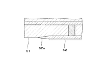
- the main part including the peripheral end (tip part) of the surface electrode 52 is formed on the surface of the outermost ceramic layer 51 constituting the ceramic multilayer substrate (Patent Document 1). 11), the peripheral end portion (tip portion) 52a of the surface electrode 52 is located at the boundary with the ceramic layer 51, and this position is a portion where the plating solution tends to remain. It tends to cause a decrease in peel strength.
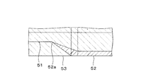
- the ceramic layer 51 and the surface electrode are also formed in the case where the peripheral end (tip portion) 52 a of the surface electrode 52 is covered with the covering ceramic layer 53 (see FIG. 2 of Patent Document 1).
- the plating solution may infiltrate from the boundary portion 53, and in that case, the plating solution penetrates to the peripheral end portion (tip portion) of the surface electrode 52 covered with the coating ceramic layer 53 and remains. There is a problem that the peel strength is reduced.
- the ceramic multilayer substrate when the ceramic multilayer substrate is subjected to a drying process with the plating solution remaining, it is exposed to a drying temperature higher than room temperature.
- a drying temperature higher than room temperature for example, when a Ni plating film (lower layer) and an Au plating (upper layer) are formed as the plating film, Ni diffuses into the Au plating film. This is because Ni has a higher ionization tendency than Au and is easily replaced with Au. The diffusion of Ni causes stains and discoloration, which may cause poor appearance.
- the plating film is a Ni plating film (lower layer) or a Sn plating film (upper layer), there is a problem that Sn is oxidized or dissolved when the drying temperature is increased.
- the present invention solves the above-described problems, and an object of the present invention is to provide a highly reliable ceramic multilayer substrate including a surface electrode having sufficient peel strength even after a plating process.
- the ceramic multilayer substrate of the present invention comprises: A ceramic multilayer substrate comprising a ceramic laminate comprising a plurality of laminated ceramic layers, and a surface electrode formed on the surface of the ceramic laminate, A concave portion is formed in a region recessed inward from the peripheral end portion of the surface electrode.
- the plating solution accumulates in the recesses (grooves) provided in the region retracted inward from the peripheral edge of the surface electrode.
- the peripheral end portion (tip portion) of the surface electrode is thin and the plating tends to be insufficient, so that if the plating solution remains there, the peripheral end portion of the surface electrode is plated.
- the interface between the ceramic and the surface electrode is eroded by the liquid and becomes the starting point of electrode destruction.
- the recesses (grooves) provided in the region where the plating solution has receded from the peripheral edge of the surface electrode )
- the surface electrode is eroded even if the film thickness of the surface electrode is thicker than the periphery and the plating solution is accumulated in the recess. The influence of the decrease in the peel strength due to is within an allowable range, and the peel strength of the surface electrode can be ensured.
- the recess is formed so as to go around the surface electrode.
- the ceramic multilayer substrate of the present invention is A ceramic multilayer substrate comprising a ceramic laminate comprising a plurality of laminated ceramic layers, and a surface electrode formed on the surface of the ceramic laminate, The elevation of the peripheral portion of the surface electrode is configured to be higher than the elevation of the central portion of the surface electrode.
- the ceramic multilayer substrate of the present invention is A ceramic multilayer substrate comprising a ceramic laminate comprising a plurality of laminated ceramic layers, a surface electrode formed on the surface of the ceramic laminate, and a coated ceramic layer covering a peripheral portion of the surface electrode. There, A concave portion is formed in the peripheral portion of the surface electrode, and the peripheral portion including a region where the peripheral end portion and the concave portion are formed is covered with the covering ceramic layer. It is said.
- the plating solution adhering in the plating process is blocked by the coating ceramic layer, and does not easily reach the peripheral edge of the surface electrode. Even when the plating solution enters from the interface between the coated ceramic layer and the surface electrode, the recessed portion is formed at a position retracted from the peripheral edge of the surface electrode. It is possible to provide a highly reliable ceramic multilayer substrate provided with a surface electrode that has a sufficient peel strength even after the plating process is difficult to reach the peripheral edge.
- the recess is formed so as to go around the surface electrode.
- the elevation of the central portion of the surface electrode that is not covered with the coating ceramic layer is lower than the elevation of the main surface of the ceramic laminate on which the surface electrode is formed. Is preferred.
- the plating solution adhering in the plating process is blocked by the coating ceramic layer, making it difficult to reach the peripheral edge including the peripheral edge (tip) of the surface electrode, and also adhering in the plating process Since the plating solution collected in the central region of the surface electrode is lower than the main surface of the ceramic laminate, the highly reliable ceramic multilayer with the surface electrode having sufficient peel strength even after the plating process It becomes possible to provide a substrate.
- the surface of the surface electrode is embedded in the surface of the ceramic laminate.
- that at least a part of the surface electrode is embedded in the surface of the ceramic laminate means that at least a part of the surface electrode is embedded in the surface of the ceramic laminate, for example, When the surface electrode is buried in the ceramic laminate leaving a predetermined exposed portion, and the exposed portion is flush with the surface of the ceramic laminate (altitude is the same), When the surface electrode is buried in the ceramic laminate leaving a predetermined exposed portion, and the elevation of the exposed portion is lower than the elevation of the ceramic laminate, The concept includes a case where a part of the surface electrode is buried in the ceramic laminate, and the elevation of the exposed portion of the surface electrode is somewhat higher than the elevation of the ceramic laminate.
- a plating film is formed on at least a part of the surface of the surface electrode.
- the ceramic multilayer substrate of the present invention even when the plating solution adheres in the plating process, corrosion by the plating solution at the peripheral edge of the surface electrode, which is likely to be the starting point of electrode destruction and electrode peeling, is suppressed, and after the plating process However, it is possible to provide a highly reliable ceramic multilayer substrate including a surface electrode having a sufficient peel strength.
- FIG. 1 It is front sectional drawing which shows the structure of the ceramic multilayer substrate concerning one Example (Example 1) of this invention. It is a figure which shows the principal part of the ceramic multilayer substrate concerning one Example (Example 1) of this invention. It is a figure explaining the manufacturing method of the ceramic multilayer substrate concerning Example 1 of this invention. It is a figure explaining the manufacturing method of the ceramic multilayer substrate concerning Example 1 of this invention. It is a figure which shows the principal part of the ceramic multilayer substrate concerning the other Example (Example 2) of this invention. It is a figure explaining the manufacturing method of the ceramic multilayer substrate concerning Example 2 of this invention. It is a figure explaining the manufacturing method of the ceramic multilayer substrate concerning Example 2 of this invention.
- (a) is a top view of the ceramic multilayer substrate concerning Example 1 of this invention
- (b) is a figure which shows the top view of a modification. It is a figure which shows the structure of the surface electrode of the ceramic multilayer substrate for a comparison. It is a figure which shows the structure of the surface electrode of the ceramic multilayer substrate for another comparison. It is a figure which shows the structure of the surface electrode of the conventional ceramic multilayer substrate. It is a figure which shows the other structure of the surface electrode of the conventional ceramic multilayer substrate.
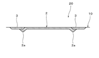
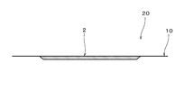
- FIG. 1 is a cross-sectional view showing a configuration of a ceramic multilayer substrate 20 according to an embodiment of the present invention
- FIG. 2 is a diagram schematically showing an enlarged main part of the ceramic multilayer substrate 20 of FIG.
- the ceramic multilayer substrate 20 includes a ceramic laminate (substrate body) 10 having a plurality of laminated ceramic layers 1 and a surface electrode (in this embodiment, Ag as a main component) formed on the surface of the ceramic laminate 10.
- a surface electrode in this embodiment, Ag as a main component
- Ag electrode 2 a coated ceramic layer 3 covering the peripheral edge 2 a of the surface electrode 2
- an internal conductor 4 such as an internal wiring 4 a and a via-hole conductor 4 b disposed inside the ceramic laminate 10. I have.
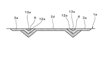
- the peripheral part 2a of the surface electrode 2 has the recessed part 12 which circulates around the surface electrode 2, the peripheral edge part (tip part) 2t of the surface electrode 2, and the surface A peripheral edge portion 2a including a region 2b in which a concave portion 12 surrounding the electrode 2 is formed is covered with a coated ceramic layer 3, and a groove 13 is also formed in the coated ceramic layer 3 in a region corresponding to the concave portion 12. ing.
- Ni plating film and an Au plating film covering the Ni plating film are formed on the surface of the central portion (exposed portion) 2c of the surface electrode 2.
- illustration of the Ni plating film and the Au plating film is omitted.
- the peripheral portion 2a of the surface electrode 2 is provided with a recess 12 that circulates the surface electrode 2, and the peripheral end (tip portion) 2t and the recess of the surface electrode 2 are provided. Since the peripheral edge portion 2a including the region 2b where 12 is formed is covered with the coating ceramic layer 3, the plating solution adhering in the plating step is blocked by the coating ceramic layer 3, and the peripheral edge portion 2a ( In particular, it becomes difficult to reach the peripheral end portion (tip portion 2t) of the surface electrode 2.
- the intruding plating solution is provided in the peripheral portion 2 a of the surface electrode 2 because the recess 12 around the surface electrode 2 is provided.
- a highly reliable ceramic multilayer substrate 20 provided with the surface electrode 2 having a sufficient peel strength is obtained.
- an electrode paste for forming a surface electrode (Ag paste in this embodiment) is applied to a ceramic green sheet 1a that becomes the ceramic layer 1 (FIGS. 1 and 2) after firing.
- An electrode paste pattern 2d is formed, and the ceramic paste pattern is coated with a ceramic paste that becomes the coated ceramic layer 3 (FIGS. 1 and 2) after firing so as to cover the peripheral portion of the electrode paste pattern 2d and expose the central portion.
- 3a is formed.
- the ceramic paste pattern 3a is disposed so as to cover a region from the outside of the peripheral end portion of the electrode paste pattern 2d to the inside of 100 ⁇ m of the peripheral end portion of the electrode paste pattern 2d.
- the resin paste that burns and decomposes and disappears in the firing process in a region retreated by 50 ⁇ m from the peripheral edge of the electrode paste pattern 2 d on the ceramic paste pattern 3 a with a width (W) of 30 ⁇ m.
- the resin paste pattern 6 is formed by applying the pattern 2d so as to circulate.
- the ceramic green sheets 1a are laminated together with other ceramic green sheets in a predetermined order so as to be the outermost layer, and then pressed to form an unfired laminated body having a flat main surface.
- the resin paste pattern 6 is provided with the ceramic paste pattern 3 a (the coated ceramic layer 3 after firing) and the electrode paste pattern 2 d (the surface electrode 2 after firing). Press.
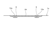
- a recess (groove) 13a is formed in the ceramic paste pattern 3a (coated ceramic layer 3 after firing), and a recess (groove) 12a is formed in the electrode paste pattern 2d (surface electrode 2 after firing).
- the electrode paste pattern 2d (firing surface electrode 2) itself is also embedded in the ceramic green sheet 1a. For this reason, the ceramic multilayer substrate 20 after firing can be reduced in height.
- the green laminate is fired to burn and decompose the resin paste pattern.
- the recess is formed after the resin paste burns and decomposes and disappears.
- the peripheral edge 2 a of the surface electrode 2 is provided with a recess 12 that circulates the surface electrode 2, and the peripheral end (tip) 2 t and the recess of the surface electrode 2.
- the ceramic multilayer substrate 20 in which the peripheral edge portion 2a including the region 2b where 12 is formed is coated with the coated ceramic layer 3 can be obtained.
- a concave portion 13 corresponding to the concave portion 12 that circulates the surface electrode 2 is also formed in the coated ceramic layer 3, but the concave portion 13 may not be formed in the coated ceramic layer 3. .
- the recess 12 can also be formed by a method of embossing the electrode paste pattern 2d after application and drying. After embossing, a ceramic multilayer substrate having a structure in which no recess is formed in the coated ceramic layer can be obtained by applying a ceramic paste.
- the recess may be formed by embossing after forming the electrode paste pattern and the ceramic paste pattern. Is possible.
- the electrode paste pattern is entirely embedded in the ceramic green sheet in the crimping step, but not all may be embedded. In that case, the exposed portion of the surface electrode is higher than the main surface of the laminate, but the basic effect of the present invention can be obtained.
- FIG. 5 is a diagram showing a main configuration of the ceramic multilayer substrate 20 according to the second embodiment of the present invention.
- a recess 12 that circulates the surface electrode 2 is formed in the peripheral edge 2 a of the surface electrode 2, and a peripheral end (tip) 2 t and a recess 12 of the surface electrode 2 are formed.
- the region 2b in which is formed is covered with a covering ceramic layer 3 having a stepped portion.
- the altitude of the central part (exposed part) 2c not covered with the covering ceramic layer 3 of the surface electrode 2 is the ceramic laminated body in which the surface electrode 2 is formed ( Substrate main body) 10 is configured to be lower than the altitude of main surface 10a.
- the altitude is a distance from the other main surface facing the main surface 10a of the ceramic laminate (substrate body) 10 to each surface.
- the surface is a surface of the ceramic laminate (substrate body) 10 on the main surface 10a side.
- the altitude of the central portion (exposed portion) 2 c that is not covered with the coated ceramic layer 3 of the surface electrode 2 is the central portion (exposed portion) of the surface electrode 2 from the other main surface of the ceramic laminate (substrate body) 10. It is the distance to the surface of 2c.
- the elevation of the main surface 10a of the ceramic laminate (substrate body) 10 on which the surface electrode 2 is formed is the main elevation of the ceramic laminate (substrate body) 10 from the other main surface of the ceramic laminate (substrate body) 10. This is the distance to the surface 10a.
- the configuration of the other parts of the ceramic multilayer substrate 20 of the second embodiment is the same as that of the ceramic multilayer substrate of the first embodiment.
- the plating solution adhering in the plating step is blocked by the coating ceramic layer 3 and the peripheral end portion (tip end) of the surface electrode 2 Part) is difficult to reach 2t, and the plating solution adhering in the plating step accumulates in the central part 2c of the surface electrode 2 having an altitude lower than that of the main surface 10a of the ceramic laminate (substrate body) 10. It is difficult to reach the peripheral end portion (tip portion) 2t of 2. Therefore, the surface electrode 2 having sufficient peel strength can be formed even after the plating process. In addition, since the central portion 2c of the surface electrode 2 is lower than the main surface 10a, the height after mounting the component can be reduced when the component using the ceramic multilayer substrate 20 is bump-connected. .
- the ceramic multilayer substrate of Example 2 can be manufactured by the following method, for example, according to the case of manufacturing the ceramic multilayer substrate of Example 1 described above.
- (1) As shown in FIG. 6, an electrode paste for forming a surface electrode is applied to a ceramic green sheet 1a to form an electrode paste pattern 2d. The peripheral portion of the electrode paste pattern 2d is covered and the central portion is exposed.
- a ceramic paste pattern 3a is formed by applying a ceramic paste that becomes a coated ceramic layer after firing.
- the ceramic paste pattern 3a is disposed so as to cover a region from the peripheral edge of the electrode paste pattern 2d to the inside of 100 ⁇ m.
- the ceramic green sheets 1a are laminated together with other ceramic green sheets in a predetermined order so as to be the outermost layer, and then pressed to form an unfired laminated body having a flat main surface.
- the resin paste pattern 6 has a ceramic paste pattern 3 a (fired coated ceramic layer 3) and an electrode paste pattern 2 d (fired surface electrode 2) located thereunder. Press.
- a recess (groove) 13a is formed in the ceramic paste pattern 3a (coated ceramic layer 3 after firing), and a recess (groove) 12a is formed in the electrode paste pattern 2d (surface electrode 2 after firing).
- the green laminate is fired to burn and decompose the resin paste pattern.
- the recess is formed after the resin paste burns and decomposes and disappears.
- the peripheral part 2a of the surface electrode 2 is provided with the concave part 12 that goes around the surface electrode 2, and the peripheral end part (tip part) 2t and the concave part 12 of the surface electrode 2 are formed.
- the laminated layer 2b is covered with a coated ceramic layer, and the elevation of the central portion (exposed portion) 2c of the surface electrode 2 that is not covered with the coated ceramic layer 3 is such that the surface electrode 2 is formed.
- the ceramic multilayer substrate 20 configured to be lower than the altitude of the main surface 10a of the (substrate body) 10 can be obtained.
- the recessed part 12 there is no special restriction
- the ceramic multilayer substrate 20 of the second embodiment for example, as shown in FIG. 8, there is a configuration in which the width of the recess (groove) formed in the surface electrode 2 is narrow.
- the ceramic multilayer substrate 20 according to this modification can be formed by slightly shifting the area where the coated ceramic layer 3 covers the surface electrode 2, that is, by slightly increasing the area of the central portion (exposed portion) 2c. Even in the ceramic multilayer substrate configured as in this modification, the same effect as in the second embodiment can be obtained.
- FIG. 9 is a diagram showing a main part of a ceramic multilayer substrate according to another embodiment (Example 3) of the present invention.
- a recess 12 that circulates the surface electrode 2 is formed in a region that recedes inward from the peripheral end (tip portion) 2 t of the surface electrode 2.
- the ceramic multilayer substrate 20 of Example 3 is not provided with a coating ceramic layer that covers the peripheral edge of the surface electrode.
- the configuration of the other parts of the ceramic multilayer substrate 20 of the third embodiment is the same as that of the ceramic multilayer substrate of the first embodiment.
- the recess 12 that circulates the surface electrode 2 is provided in the region retracted inward from the peripheral end (tip portion) 2t of the surface electrode 2, in the plating step Even when the plating solution adheres, the plating solution accumulates in the recesses (grooves) 12 provided in the region retracted inward from the peripheral end portion (tip portion) 2t of the surface electrode 2.
- the peripheral edge portion (tip portion) 2t of the surface electrode 2 that is likely to become rust is suppressed from being corroded by the plating solution, and is highly reliable with the surface electrode 2 having sufficient peel strength even after the plating process.
- a ceramic multilayer substrate can be provided.
- the peripheral end (tip portion) 2t of the surface electrode 2 is thin and the plating tends to be insufficient, if the plating solution remains, the peripheral end (tip portion) 2t of the surface electrode 2 is plated.
- the interface between the ceramic layer 1 and the surface electrode 2 is eroded by the liquid and becomes a starting point of electrode destruction, but the region receding from the peripheral end 2a of the surface electrode 2 where the recess 12 is formed Even if the film thickness of the electrode 2 is thicker than the peripheral edge portion 2a and the plating solution is accumulated in the recess 12, the influence on the decrease in the peeling strength due to the erosion of the surface electrode 2 is within an allowable range, and the peeling of the surface electrode 2 Strength can be secured.
- the ceramic multilayer substrate 20 of Example 3 can be manufactured, for example, by the following method. (1) First, as shown in FIG. 10, an electrode paste pattern 2d is formed by applying an electrode paste for forming a surface electrode to the ceramic green sheet 1a.
- the resin paste that burns and decomposes and disappears in the firing process in a region 50 ⁇ m backward from the peripheral edge of the electrode paste pattern 2 d on the ceramic paste pattern 3 a with a width (W) of 50 ⁇ m.
- the resin paste pattern 6 is formed by applying the pattern 2d so as to circulate.
- the ceramic green sheets 1a are laminated together with other ceramic green sheets in a predetermined order so as to be the outermost layer, and then pressed to form an unfired laminated body having a flat main surface.
- this crimping step as shown in FIG. 11, as a result of the resin paste pattern 6 pressing the electrode paste pattern 2d (firing surface electrode 2) located thereunder, the electrode paste pattern 2d (firing surface after firing) A recess (groove) 12a is formed in the electrode 2).
- the electrode paste pattern 2d (firing surface electrode 2) itself is also embedded in the ceramic green sheet 1a. For this reason, the ceramic multilayer substrate 20 after firing can be reduced in height.
- the green laminate is fired to burn and decompose the resin paste pattern.
- the recess is formed after the resin paste burns and decomposes and disappears.
- the electrode paste pattern is entirely embedded in the ceramic green sheet in the crimping step. However, not all of the electrode paste pattern may be embedded. In that case, a part of the surface electrode becomes higher than the main surface of the laminate, but the basic effect of the present invention can be obtained.
- FIG. 12 is a diagram showing a main part of a ceramic multilayer substrate according to another embodiment (Example 4) of the present invention.
- the elevation of the peripheral edge 2a of the surface electrode 2 is configured to be higher than the elevation of the central portion (exposed portion) 2c of the surface electrode 2.
- the ceramic multilayer substrate 20 of Example 4 is not provided with a coating ceramic layer that covers the peripheral portion of the surface electrode.
- the configuration of the other parts of the ceramic multilayer substrate 20 of the fourth embodiment is the same as that of the ceramic multilayer substrate of the first embodiment.
- the elevation of the peripheral portion 2a of the surface electrode 2 is made higher than the elevation of the central portion 2c of the surface electrode 2, and the central portion 2c has an elevation higher than that of the peripheral portion 2a. Since it is configured to be low, even if the plating solution remains after the plating step, the plating solution is accumulated in the central portion 2c inside the peripheral portion 2a, so that sufficient peel strength is obtained even after the plating step. It is possible to provide a highly reliable ceramic multilayer substrate 20 including the surface electrode 2 having the following.
- the ceramic multilayer substrate 20 of Example 4 can be manufactured by the following method, for example. (1) First, as shown in FIG. 13, an electrode paste pattern 2d is formed by applying an electrode paste for forming a surface electrode to the ceramic green sheet 1a.
- the ceramic green sheets 1a are laminated together with other ceramic green sheets in a predetermined order so as to be the outermost layer, and then pressed to form an unfired laminated body having a flat main surface.
- the resin paste pattern 6 presses the electrode paste pattern 2d (firing surface electrode 2) positioned therebelow, as a result of which the electrode paste pattern 2d ( The whole center part except the peripheral part of the surface electrode 2) after baking becomes a recessed shape.
- the electrode paste pattern 2d (surface electrode 2 after firing) itself is also embedded in the ceramic green sheet. For this reason, the ceramic multilayer substrate 20 after firing can be reduced in height.
- the green laminate is fired to burn and decompose the resin paste pattern.
- the recess is formed after the resin paste burns and decomposes and disappears.
- the ceramic multilayer substrate 20 including the surface electrode 2 having a structure in which the elevation of the peripheral edge portion 2a of the surface electrode 2 is higher than the elevation of the central portion (exposed portion) 2c of the surface electrode 2 is provided. Is obtained.
- the electrode paste pattern is entirely embedded in the ceramic green sheet in the crimping step. However, not all of the electrode paste pattern may be embedded. In that case, a part of the surface electrode (for example, the peripheral portion) becomes higher than the main surface of the laminate, but the basic effect of the present invention can be obtained.
- the peel strength of the surface electrode was examined for the ceramic multilayer substrate produced in each of the above examples.
- a 2 mm square surface electrode was formed, and the peel strength of this surface electrode was measured.
- 2 mm square is a square having a side of 2 mm.
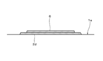
- a ceramic multilayer substrate 20 in which a surface electrode 2 having a structure in which a peripheral edge 2a is covered with a covering ceramic layer 3 is provided on the surface of a ceramic laminate (substrate body) 10 as shown in FIG. (Comparative Example 1)
- the peel strength (N / 2mm ⁇ ) of the surface electrode was examined. The peel strength is obtained by measuring the peel strength of the surface electrode when a predetermined copper wire is soldered to the surface electrode and the copper wire is pulled in a direction perpendicular to the surface electrode. The results are shown in Table 1.
- each sample of Table 1 is as follows.
- Comparative example (conventional example) 1 FIG. 16 shows a ceramic multilayer substrate provided with a surface electrode whose peripheral edge is covered with a coating ceramic layer.
- Comparative example (conventional example) 2 FIG. 17 shows a ceramic multilayer substrate provided with a surface electrode not coated with a coated ceramic layer.
- Sample 1 of Example Ceramic multilayer substrate provided with the surface electrode of FIGS. 1 and 2 manufactured in Example 1 (4) Sample 2-1 of Example Ceramic multilayer substrate provided with the surface electrode of FIG. 5 produced in Example 2 (5)
- Sample 3 of Example The ceramic multilayer substrate provided with the surface electrode of FIG. 9 produced in Example 3 (7) Sample 4 of Example The ceramic multilayer substrate provided with the surface electrode of FIG.
- the peel strength of the surface electrode was insufficient at 22 N / 2 mm ⁇ and 20 N / 2 mm ⁇ . However, it was confirmed that the peel strength of the surface electrode was significantly improved to 27 to 34 N / 2 mm ⁇ in the ceramic multilayer substrate produced in Examples 1 to 4 and satisfying the requirements of the present invention. .
- the present invention is not limited to each of the above-described embodiments.
- the constituent material of the surface electrode, the specific shape, the number and arrangement of the arrangement, the arrangement when the coating ceramic layer is provided, the coating ceramic Within the scope of the invention, there are various compositions relating to the specific composition of the ceramic constituting the layer, the number of laminated ceramic layers constituting the ceramic substrate, the arrangement of internal conductors, the specific composition of the ceramic constituting the ceramic substrate, etc. It is possible to add applications and modifications.
- the peripheral portion 2a of the surface electrode 2 is formed with a recess 12 that circulates the surface electrode 2, and when viewed from the top in the stacking direction of the ceramic multilayer substrate 20, FIG. As shown in (a).
- the surface electrode having sufficient peel strength not only when the recess is formed so as to circulate around the surface electrode but also when the recess is formed at a part of the peripheral edge of the surface electrode. Can be formed.
- the surface electrode 2 having sufficient peel strength can be formed by forming the recesses 12 at the peripheral edges of the two opposite sides of the surface electrode 2.
Landscapes
- Engineering & Computer Science (AREA)
- Microelectronics & Electronic Packaging (AREA)
- Chemical & Material Sciences (AREA)
- Ceramic Engineering (AREA)
- Inorganic Chemistry (AREA)
- Manufacturing & Machinery (AREA)
- Production Of Multi-Layered Print Wiring Board (AREA)
- Ceramic Capacitors (AREA)
- Fixed Capacitors And Capacitor Manufacturing Machines (AREA)
- Manufacturing Of Printed Wiring (AREA)
Abstract
La présente invention concerne un substrat céramique multicouche haute fiabilité doté d'une électrode de surface possédant une résistance au pelage suffisante, même après avoir subi une étape de dépôt électrolytique. Ce substrat céramique multicouche, qui est doté d'un stratifié céramique doté d'une pluralité de couches céramiques stratifiées, d'une électrode de surface formée à la surface du stratifié céramique, et d'une couche de céramique revêtue obtenue par le revêtement de la périphérie de l'électrode de surface, est conçu de sorte que des évidements (12) qui entourent l'électrode de surface soient formés sur la périphérie (2a) de l'électrode de surface (2), et la périphérie de l'électrode de surface, qui contient des régions dans lesquelles les évidements et les extrémités périphériques sont recouverts par la couche céramique revêtue (3). Le substrat céramique multicouche est en outre conçu de sorte que l'élévation d'une section centrale, qui n'est pas recouverte par la couche de céramique revêtue de l'électrode de surface, soit plus petite que l'élévation de la surface principale du stratifié céramique sur lequel est formée l'électrode de surface.
Priority Applications (3)
| Application Number | Priority Date | Filing Date | Title |
|---|---|---|---|
| CN201280016076.2A CN103460818B (zh) | 2011-03-25 | 2012-03-13 | 陶瓷多层基板 |
| JP2013507358A JP5590223B2 (ja) | 2011-03-25 | 2012-03-13 | セラミック多層基板 |
| US13/975,568 US9681534B2 (en) | 2011-03-25 | 2013-08-26 | Ceramic multilayer substrate |
Applications Claiming Priority (2)
| Application Number | Priority Date | Filing Date | Title |
|---|---|---|---|
| JP2011067873 | 2011-03-25 | ||
| JP2011-067873 | 2011-03-25 |
Related Child Applications (1)
| Application Number | Title | Priority Date | Filing Date |
|---|---|---|---|
| US13/975,568 Continuation US9681534B2 (en) | 2011-03-25 | 2013-08-26 | Ceramic multilayer substrate |
Publications (1)
| Publication Number | Publication Date |
|---|---|
| WO2012132880A1 true WO2012132880A1 (fr) | 2012-10-04 |
Family
ID=46930618
Family Applications (1)
| Application Number | Title | Priority Date | Filing Date |
|---|---|---|---|
| PCT/JP2012/056425 WO2012132880A1 (fr) | 2011-03-25 | 2012-03-13 | Substrat céramique multicouche |
Country Status (4)
| Country | Link |
|---|---|
| US (1) | US9681534B2 (fr) |
| JP (1) | JP5590223B2 (fr) |
| CN (1) | CN103460818B (fr) |
| WO (1) | WO2012132880A1 (fr) |
Cited By (5)
| Publication number | Priority date | Publication date | Assignee | Title |
|---|---|---|---|---|
| JP2010192547A (ja) * | 2009-02-16 | 2010-09-02 | Ngk Spark Plug Co Ltd | 多層配線基板及びその製造方法 |
| WO2018212119A1 (fr) * | 2017-05-15 | 2018-11-22 | 株式会社村田製作所 | Composant électronique empilé et procédé de fabrication de composant électronique empilé |
| WO2018216452A1 (fr) * | 2017-05-23 | 2018-11-29 | 株式会社村田製作所 | Composant électronique et procédé de fabrication de composant électronique |
| WO2020004345A1 (fr) * | 2018-06-28 | 2020-01-02 | 株式会社フジクラ | Composant passif haute fréquence |
| WO2023048212A1 (fr) * | 2021-09-24 | 2023-03-30 | 株式会社村田製作所 | Composant électronique |
Families Citing this family (3)
| Publication number | Priority date | Publication date | Assignee | Title |
|---|---|---|---|---|
| WO2012121141A1 (fr) * | 2011-03-07 | 2012-09-13 | 株式会社村田製作所 | Substrat multicouche en céramique et son procédé de fabrication |
| KR102493465B1 (ko) * | 2016-03-22 | 2023-01-30 | 삼성전자 주식회사 | 인쇄회로기판 및 이를 가지는 반도체 패키지 |
| DE102020201869A1 (de) | 2020-02-14 | 2021-08-19 | Robert Bosch Gesellschaft mit beschränkter Haftung | Schaltungsträger mit einer keramischen Lotstopp-Barriere |
Citations (7)
| Publication number | Priority date | Publication date | Assignee | Title |
|---|---|---|---|---|
| JPH10209612A (ja) * | 1997-01-24 | 1998-08-07 | Shinko Electric Ind Co Ltd | 回路基板およびその製造方法 |
| JP2004200608A (ja) * | 2002-12-20 | 2004-07-15 | Fujikura Ltd | プリント配線基板およびその製造方法 |
| JP2007036059A (ja) * | 2005-07-28 | 2007-02-08 | Sharp Corp | 半田付け実装構造およびその製造方法、並びにその利用 |
| JP2008091874A (ja) * | 2006-09-08 | 2008-04-17 | Alps Electric Co Ltd | セラミック回路基板とその製造方法 |
| JP2008263125A (ja) * | 2007-04-13 | 2008-10-30 | Shinko Electric Ind Co Ltd | 配線基板の製造方法及び半導体装置の製造方法及び配線基板 |
| JP2010074153A (ja) * | 2008-08-21 | 2010-04-02 | Nec Electronics Corp | 電子部品製造方法、電子部品、及び、冶具 |
| JP2011049342A (ja) * | 2009-08-27 | 2011-03-10 | Kyocera Corp | 電子部品搭載用基板およびその製造方法 |
Family Cites Families (13)
| Publication number | Priority date | Publication date | Assignee | Title |
|---|---|---|---|---|
| JPH01259540A (ja) | 1988-04-08 | 1989-10-17 | Sharp Corp | 半導体装置 |
| JPH0225045A (ja) | 1988-07-13 | 1990-01-26 | Oki Electric Ind Co Ltd | 半導体装置 |
| JPH08213756A (ja) | 1995-02-03 | 1996-08-20 | Matsushita Electric Ind Co Ltd | セラミック多層基板 |
| JPH11204941A (ja) | 1998-01-14 | 1999-07-30 | Hitachi Ltd | 回路基板の製造方法 |
| US6800815B1 (en) * | 2001-01-16 | 2004-10-05 | National Semiconductor Corporation | Materials and structure for a high reliability bga connection between LTCC and PB boards |
| JP3651413B2 (ja) * | 2001-05-21 | 2005-05-25 | 日立電線株式会社 | 半導体装置用テープキャリア及びそれを用いた半導体装置、半導体装置用テープキャリアの製造方法及び半導体装置の製造方法 |
| JP3615727B2 (ja) * | 2001-10-31 | 2005-02-02 | 新光電気工業株式会社 | 半導体装置用パッケージ |
| TWI245402B (en) * | 2002-01-07 | 2005-12-11 | Megic Corp | Rod soldering structure and manufacturing process thereof |
| WO2003071843A1 (fr) | 2002-02-22 | 2003-08-28 | Fujikura Ltd. | Tableau de connexions multicouche, base pour tableau de connexions multicouche, tableau de connexions imprime et son procede de production |
| JP3994936B2 (ja) * | 2002-07-16 | 2007-10-24 | 株式会社村田製作所 | 積層型セラミック電子部品およびその製造方法 |
| JP3990962B2 (ja) * | 2002-09-17 | 2007-10-17 | 新光電気工業株式会社 | 配線基板の製造方法 |
| US7088008B2 (en) * | 2003-03-20 | 2006-08-08 | International Business Machines Corporation | Electronic package with optimized circuitization pattern |
| WO2012121141A1 (fr) * | 2011-03-07 | 2012-09-13 | 株式会社村田製作所 | Substrat multicouche en céramique et son procédé de fabrication |
-
2012
- 2012-03-13 JP JP2013507358A patent/JP5590223B2/ja active Active
- 2012-03-13 CN CN201280016076.2A patent/CN103460818B/zh active Active
- 2012-03-13 WO PCT/JP2012/056425 patent/WO2012132880A1/fr active Application Filing
-
2013
- 2013-08-26 US US13/975,568 patent/US9681534B2/en active Active
Patent Citations (7)
| Publication number | Priority date | Publication date | Assignee | Title |
|---|---|---|---|---|
| JPH10209612A (ja) * | 1997-01-24 | 1998-08-07 | Shinko Electric Ind Co Ltd | 回路基板およびその製造方法 |
| JP2004200608A (ja) * | 2002-12-20 | 2004-07-15 | Fujikura Ltd | プリント配線基板およびその製造方法 |
| JP2007036059A (ja) * | 2005-07-28 | 2007-02-08 | Sharp Corp | 半田付け実装構造およびその製造方法、並びにその利用 |
| JP2008091874A (ja) * | 2006-09-08 | 2008-04-17 | Alps Electric Co Ltd | セラミック回路基板とその製造方法 |
| JP2008263125A (ja) * | 2007-04-13 | 2008-10-30 | Shinko Electric Ind Co Ltd | 配線基板の製造方法及び半導体装置の製造方法及び配線基板 |
| JP2010074153A (ja) * | 2008-08-21 | 2010-04-02 | Nec Electronics Corp | 電子部品製造方法、電子部品、及び、冶具 |
| JP2011049342A (ja) * | 2009-08-27 | 2011-03-10 | Kyocera Corp | 電子部品搭載用基板およびその製造方法 |
Cited By (13)
| Publication number | Priority date | Publication date | Assignee | Title |
|---|---|---|---|---|
| JP2010192547A (ja) * | 2009-02-16 | 2010-09-02 | Ngk Spark Plug Co Ltd | 多層配線基板及びその製造方法 |
| US11152157B2 (en) | 2017-05-15 | 2021-10-19 | Murata Manufacturing Co., Ltd. | Stacked electronic component and method for manufacturing stacked electronic component |
| KR20190100393A (ko) * | 2017-05-15 | 2019-08-28 | 가부시키가이샤 무라타 세이사쿠쇼 | 적층형 전자부품 및 적층형 전자부품의 제조 방법 |
| JPWO2018212119A1 (ja) * | 2017-05-15 | 2020-03-12 | 株式会社村田製作所 | 積層型電子部品および積層型電子部品の製造方法 |
| KR102267242B1 (ko) * | 2017-05-15 | 2021-06-21 | 가부시키가이샤 무라타 세이사쿠쇼 | 적층형 전자부품 및 적층형 전자부품의 제조 방법 |
| WO2018212119A1 (fr) * | 2017-05-15 | 2018-11-22 | 株式会社村田製作所 | Composant électronique empilé et procédé de fabrication de composant électronique empilé |
| WO2018216452A1 (fr) * | 2017-05-23 | 2018-11-29 | 株式会社村田製作所 | Composant électronique et procédé de fabrication de composant électronique |
| JPWO2018216452A1 (ja) * | 2017-05-23 | 2020-03-12 | 株式会社村田製作所 | 電子部品、及び、電子部品の製造方法 |
| JP2021141341A (ja) * | 2017-05-23 | 2021-09-16 | 株式会社村田製作所 | 電子部品 |
| JP7131658B2 (ja) | 2017-05-23 | 2022-09-06 | 株式会社村田製作所 | 電子部品 |
| US11450483B2 (en) | 2017-05-23 | 2022-09-20 | Murata Manufacturing Co., Ltd. | Electronic component with baked electrodes and having a continuously curved recess |
| WO2020004345A1 (fr) * | 2018-06-28 | 2020-01-02 | 株式会社フジクラ | Composant passif haute fréquence |
| WO2023048212A1 (fr) * | 2021-09-24 | 2023-03-30 | 株式会社村田製作所 | Composant électronique |
Also Published As
| Publication number | Publication date |
|---|---|
| CN103460818B (zh) | 2017-08-04 |
| CN103460818A (zh) | 2013-12-18 |
| JP5590223B2 (ja) | 2014-09-17 |
| US20130341080A1 (en) | 2013-12-26 |
| JPWO2012132880A1 (ja) | 2014-07-28 |
| US9681534B2 (en) | 2017-06-13 |
Similar Documents
| Publication | Publication Date | Title |
|---|---|---|
| JP5590223B2 (ja) | セラミック多層基板 | |
| JP5217677B2 (ja) | 積層セラミック電子部品およびその製造方法 | |
| JP5532027B2 (ja) | 積層セラミック電子部品およびその製造方法 | |
| JP5273122B2 (ja) | 電子部品及び電子部品の製造方法 | |
| JP4636180B2 (ja) | 積層型セラミック電子部品 | |
| JP2008300769A5 (fr) | ||
| JP2017028013A (ja) | 積層セラミックコンデンサ | |
| TW201740397A (zh) | 電子零件 | |
| JP6020503B2 (ja) | 積層セラミック電子部品 | |
| WO2006126333A1 (fr) | Composant électronique céramique multicouche et procédé de fabrication idoine | |
| JP2012094820A (ja) | 積層セラミック電子部品 | |
| CN112614697B (zh) | 层叠陶瓷电容器 | |
| CN104952618A (zh) | 层叠陶瓷电子部件 | |
| JP2012009679A (ja) | セラミック電子部品及びその製造方法 | |
| KR20190124128A (ko) | 플렉시블 프린트 배선판, 접속체의 제조 방법 및 접속체 | |
| US20180130577A1 (en) | Ntc thermistor to be embedded in a substrate, and method for producing the same | |
| JP5737388B2 (ja) | ガラスセラミック基板およびその製造方法 | |
| US20230197350A1 (en) | Multilayer ceramic capacitor | |
| US20230197345A1 (en) | Multilayer ceramic capacitor | |
| US20230197346A1 (en) | Multilayer ceramic capacitor | |
| JP2012009556A (ja) | セラミック電子部品及びその製造方法 | |
| US20230197339A1 (en) | Multilayer ceramic capacitor | |
| JP2015043424A (ja) | 積層セラミックコンデンサ | |
| JP2019106443A (ja) | 積層セラミックコンデンサおよびその製造方法 | |
| US9111691B2 (en) | Ceramic electronic component |
Legal Events
| Date | Code | Title | Description |
|---|---|---|---|
| 121 | Ep: the epo has been informed by wipo that ep was designated in this application |
Ref document number: 12764814 Country of ref document: EP Kind code of ref document: A1 |
|
| ENP | Entry into the national phase |
Ref document number: 2013507358 Country of ref document: JP Kind code of ref document: A |
|
| NENP | Non-entry into the national phase |
Ref country code: DE |
|
| 122 | Ep: pct application non-entry in european phase |
Ref document number: 12764814 Country of ref document: EP Kind code of ref document: A1 |