WO2011070741A1 - Cvd用トレーおよびそれを用いた成膜方法 - Google Patents
Cvd用トレーおよびそれを用いた成膜方法 Download PDFInfo
- Publication number
- WO2011070741A1 WO2011070741A1 PCT/JP2010/006943 JP2010006943W WO2011070741A1 WO 2011070741 A1 WO2011070741 A1 WO 2011070741A1 JP 2010006943 W JP2010006943 W JP 2010006943W WO 2011070741 A1 WO2011070741 A1 WO 2011070741A1
- Authority
- WO
- WIPO (PCT)
- Prior art keywords
- tray
- silicon wafer
- support member
- cvd
- film
- Prior art date
- Legal status (The legal status is an assumption and is not a legal conclusion. Google has not performed a legal analysis and makes no representation as to the accuracy of the status listed.)
- Ceased
Links
Images





Classifications
-
- C—CHEMISTRY; METALLURGY
- C23—COATING METALLIC MATERIAL; COATING MATERIAL WITH METALLIC MATERIAL; CHEMICAL SURFACE TREATMENT; DIFFUSION TREATMENT OF METALLIC MATERIAL; COATING BY VACUUM EVAPORATION, BY SPUTTERING, BY ION IMPLANTATION OR BY CHEMICAL VAPOUR DEPOSITION, IN GENERAL; INHIBITING CORROSION OF METALLIC MATERIAL OR INCRUSTATION IN GENERAL
- C23C—COATING METALLIC MATERIAL; COATING MATERIAL WITH METALLIC MATERIAL; SURFACE TREATMENT OF METALLIC MATERIAL BY DIFFUSION INTO THE SURFACE, BY CHEMICAL CONVERSION OR SUBSTITUTION; COATING BY VACUUM EVAPORATION, BY SPUTTERING, BY ION IMPLANTATION OR BY CHEMICAL VAPOUR DEPOSITION, IN GENERAL
- C23C16/00—Chemical coating by decomposition of gaseous compounds, without leaving reaction products of surface material in the coating, i.e. chemical vapour deposition [CVD] processes
- C23C16/44—Chemical coating by decomposition of gaseous compounds, without leaving reaction products of surface material in the coating, i.e. chemical vapour deposition [CVD] processes characterised by the method of coating
- C23C16/458—Chemical coating by decomposition of gaseous compounds, without leaving reaction products of surface material in the coating, i.e. chemical vapour deposition [CVD] processes characterised by the method of coating characterised by the method used for supporting substrates in the reaction chamber
-
- C—CHEMISTRY; METALLURGY
- C23—COATING METALLIC MATERIAL; COATING MATERIAL WITH METALLIC MATERIAL; CHEMICAL SURFACE TREATMENT; DIFFUSION TREATMENT OF METALLIC MATERIAL; COATING BY VACUUM EVAPORATION, BY SPUTTERING, BY ION IMPLANTATION OR BY CHEMICAL VAPOUR DEPOSITION, IN GENERAL; INHIBITING CORROSION OF METALLIC MATERIAL OR INCRUSTATION IN GENERAL
- C23C—COATING METALLIC MATERIAL; COATING MATERIAL WITH METALLIC MATERIAL; SURFACE TREATMENT OF METALLIC MATERIAL BY DIFFUSION INTO THE SURFACE, BY CHEMICAL CONVERSION OR SUBSTITUTION; COATING BY VACUUM EVAPORATION, BY SPUTTERING, BY ION IMPLANTATION OR BY CHEMICAL VAPOUR DEPOSITION, IN GENERAL
- C23C16/00—Chemical coating by decomposition of gaseous compounds, without leaving reaction products of surface material in the coating, i.e. chemical vapour deposition [CVD] processes
- C23C16/44—Chemical coating by decomposition of gaseous compounds, without leaving reaction products of surface material in the coating, i.e. chemical vapour deposition [CVD] processes characterised by the method of coating
- C23C16/458—Chemical coating by decomposition of gaseous compounds, without leaving reaction products of surface material in the coating, i.e. chemical vapour deposition [CVD] processes characterised by the method of coating characterised by the method used for supporting substrates in the reaction chamber
- C23C16/4582—Rigid and flat substrates, e.g. plates or discs
- C23C16/4583—Rigid and flat substrates, e.g. plates or discs the substrate being supported substantially horizontally
- C23C16/4585—Devices at or outside the perimeter of the substrate support, e.g. clamping rings, shrouds
-
- H—ELECTRICITY
- H10—SEMICONDUCTOR DEVICES; ELECTRIC SOLID-STATE DEVICES NOT OTHERWISE PROVIDED FOR
- H10P—GENERIC PROCESSES OR APPARATUS FOR THE MANUFACTURE OR TREATMENT OF DEVICES COVERED BY CLASS H10
- H10P14/00—Formation of materials, e.g. in the shape of layers or pillars
- H10P14/20—Formation of materials, e.g. in the shape of layers or pillars of semiconductor materials
- H10P14/24—Formation of materials, e.g. in the shape of layers or pillars of semiconductor materials using chemical vapour deposition [CVD]
Definitions
- the present invention relates to a CVD tray used for film formation by a CVD method, and a film formation method using the same, and more specifically, a uniform thickness distribution of an oxide film formed on the surface of the silicon wafer.
- the present invention relates to a CVD tray and a film forming method using the same.
- a protective film or an insulating film is formed on a silicon wafer.
- an oxide film or the like is formed as an interlayer insulating film on the surface side of a silicon wafer used as a device creation region, and thereafter, wiring formation or the like is performed.
- the silicon single crystal substrate is formed from the back surface of the silicon single crystal substrate.
- an atmospheric pressure CVD method is used.
- the atmospheric pressure CVD method after the silicon wafer is placed on the tray with the surface to be deposited facing up, the tray and the silicon wafer are heated while supplying the source gas onto the silicon wafer. The components are deposited on a silicon wafer to form a film.
- the atmospheric pressure CVD method is widely used when forming an oxide film because the film formation speed is fast, so the time required for forming the oxide film can be shortened, and by incorporating a transfer device, This is because an oxide film can be formed on a silicon wafer.
- a mixed gas of monosilane (SiH 4 ) and oxygen (O 2 ), tetraethoxysilane (TEOS, chemical formula: Si (OC 2 H 5 ) 4 ) and ozone (O 3 ) are used as source gases. ) Is used.
- the tray on which the silicon wafer is placed when forming the oxide film by the atmospheric pressure CVD method is required not to be deformed by heating at the time of film formation and to cause no contamination on the silicon wafer.
- the tray one obtained by sintering SiC or one whose surface is further coated with a SiC film is used.
- a flat mounting portion for supporting a silicon wafer is used.
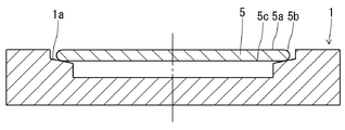
- FIG. 10 is a cross-sectional view showing a state in which a silicon wafer is placed on a tray in which the conventional placement portion is flat.
- the tray 1 shown in FIG. 10 has a flat placement portion 1a on which the silicon wafer 5 is placed.
- the silicon wafer 5 is placed on the tray 1, the silicon wafer is not formed. Since the surface 5c comes into contact with the tray mounting portion 1a, scratches occur over the entire surface of the non-film-forming surface 5c of the silicon wafer.
- the depth of contact scratches varies slightly depending on the film forming conditions, but contact scratches with a depth of about 3 to 10 ⁇ m are generated.
- Patent Document 1 uses a tray that supports the outer peripheral portion of the silicon wafer.
- FIG. 11 is a cross-sectional view showing a state in which a silicon wafer is placed on a tray that supports the outer periphery of a conventional silicon wafer.
- the tray 1 shown in FIG. 11 has a taper-shaped mounting portion 1a.
- the mounting portion 1a supports the outer peripheral portion 5b of the silicon wafer, and the silicon wafer 5 is mounted on the tray 1.
- the silicon wafer When a tray that supports the outer periphery of the silicon wafer is used, the silicon wafer is supported without contact between the non-film-formation surface 5c of the silicon wafer and the tray 1, so that the occurrence of contact scratches can be greatly reduced. .
- the non-film-forming surface side is polished on one side while holding the film-forming surface, so if the oxide film thickness distribution is non-uniform, the wafer is held elastically deformed and non-uniform after polishing. Since the oxide thickness distribution is transferred to the non-deposition surface, the flatness of the silicon wafer is deteriorated. The deterioration of the flatness increases as the polishing amount increases, and affects the flatness of the epitaxial wafer formed thereafter.
- the present invention has been made in view of such a situation, and when used for film formation by an atmospheric pressure CVD method, contact scratches do not occur on the non-film-formation surface of the silicon wafer, and the silicon wafer is not damaged. It is an object of the present invention to provide a CVD tray capable of making the thickness distribution of an oxide film to be formed uniform and a film forming method using the same.
- the tray was composed of a tray body and a support member that was installed on the tray body and supported a silicon wafer.
- the support member is provided with a placement portion for directly placing the silicon wafer, and the placement portion has a placement portion lower surface separated from the tray main body, thereby reducing the thickness distribution of the oxide film formed on the silicon wafer. It was found that it can be made uniform.
- the mounting portion is formed with an inclined surface, and the inner circumferential side thereof is disposed so as to be close to the surface of the opposing tray body with a distance from the silicon wafer to be mounted. It was clarified that the thickness distribution of the oxide film formed on the silicon wafer can be made uniform without causing contact scratches on the silicon wafer by supporting the outer periphery of the silicon wafer.
- the thickness distribution of the oxide film formed on the silicon wafer can be made more uniform by making the tray a structure that reduces the contact area between the support member and the tray body.
- the present invention has been completed on the basis of the above findings, and the gist of the present invention is the following CVD trays (1) to (9) and the following film forming method (10).
- a tray used for film formation by a CVD method comprising a tray body and a support member that is supported by the tray body and supports a silicon wafer, and the silicon wafer is directly placed on the support member
- the mounting portion is provided, and the mounting portion further includes a lower surface of the mounting portion that is spaced from the surface of the tray body that faces the silicon wafer to be placed and is opposite to the mounting surface. Tray.
- the tray main body is provided with a projecting portion, and the support member is installed on the projecting portion. tray.
- the tray according to the above (2) further includes a jig for supporting the support member, and the support member is configured to be configured to reduce the contact area through point contact or line contact with the jig. And a CVD tray having a structure for erection on the tray body.
- the tray main body has a concave receiving portion for receiving the support member, the inner peripheral surface of the receiving portion is an inclined surface, and the upper portion thereof is disposed away from the center of the receiving portion.
- the placing portion is formed with an inclined surface, and the inner circumferential side thereof is disposed so as to approach the surface of the tray body facing the silicon wafer on which the opposite side is placed,
- the CVD tray according to any one of (1) to (6) above, which supports the outer periphery of a silicon wafer.
- a film forming method for forming a film on the silicon wafer by a CVD method by heating the silicon wafer while supplying a raw material gas onto the silicon wafer after placing the silicon wafer on a tray A film forming method using the CVD tray according to any one of (1) to (9) as the tray.
- the CVD tray of the present invention separates the tray main body from the placement portion of the support member that supports the silicon wafer, so that when used for film formation on a silicon wafer by the atmospheric pressure CVD method, Heat conduction to the outer peripheral portion of the silicon wafer can be reduced, and the thickness distribution of the formed oxide film can be made uniform.
- the mounting portion is formed with an inclined surface, and the inner circumferential side thereof is disposed so as to approach the surface of the tray main body opposite to the silicon wafer to be mounted, and by supporting the outer peripheral portion of the silicon wafer, When used for film formation on a silicon wafer by the atmospheric pressure CVD method, the thickness distribution of the formed oxide film can be made uniform without causing contact scratches on the non-film formation surface of the silicon wafer.
- the heat conduction from the tray main body to the support member is reduced by making the tray a structure that reduces the contact area between the support member and the tray main body, the heat conduction from the mounting portion to the outer peripheral portion of the silicon wafer is reduced.
- the thickness distribution of the oxide film to be formed can be made more uniform.
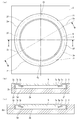
- FIG. 1 is a view showing an embodiment comprising a tray main body and a support member of the present invention.
- FIG. 1 (a) shows a case where the tray main body has a receiving portion
- FIG. 1 (b) shows a flat tray main body.
- FIG. 1 (c) uses a flat tray body, and when the support member is supported in the middle,
- FIG. 1 (d) shows the surface of the tray body opposite to the silicon wafer. The case where a recessed part is provided is shown, respectively.
- FIG. 2 is a view showing an embodiment in which a protruding portion is provided on the tray body of the present invention
- FIG. 2 (a) is a top view
- FIG. 2 (b) is an AA cross-sectional view in FIG.
- FIG. 2C is a cross-sectional view taken along the line BB in FIG.
- FIG. 3 is a cross-sectional view showing an embodiment in which a protruding portion is provided on the tray body of the present invention.
- FIG. 3A shows a case where a planar tray body is used
- FIG. 3 (c) shows a case where a concave portion is provided below the placement portion.
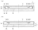
- FIG. 4 is a view showing an embodiment in which a support member is installed through point contact and line contact of the present invention
- FIG. 4 (a) is a top view
- FIG. 4 (b) is A in FIG. 4 (a).
- FIG. 5 is a cross-sectional view showing an embodiment in which a support member is installed via line contact according to the present invention
- FIG. 5 (a) shows a case where a tray body having a concave receiving portion is installed via line contact.
- FIG. 5B shows a case where the flat tray body is installed via line contact.
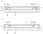
- FIG. 6 is a cross-sectional view showing an embodiment in which a support member is installed through point contact or line contact by the jig of the present invention
- FIG. 6 (a) shows a case where the support member is installed through point contact.
- FIG. 6B shows a case where the supporting member is installed via line contact.
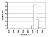
- FIG. 7 is a view showing the thickness distribution of an oxide film when formed on a silicon wafer using the CVD tray of the present invention.
- FIG. 8 is a diagram showing a thickness distribution of an oxide film when a film is formed on a silicon wafer using a tray that supports a conventional outer periphery of the silicon wafer.
- FIG. 9 is a diagram showing a thickness distribution of an oxide film formed when a film having a structure for reducing a contact area or a tray having no structure is formed by a CVD method.
- FIG. 10 is a cross-sectional view showing a state in which a silicon wafer is placed on a tray with a conventional placing portion being flat.
- FIG. 11 is a cross-sectional view showing a state in which a silicon wafer is placed on a tray that supports the outer periphery of a conventional silicon wafer.
- FIG. 1 is a view showing an embodiment comprising a tray main body and a support member of the present invention.
- FIG. 1 (a) shows a case where the tray main body has a receiving portion
- FIG. 1 (b) shows a flat tray main body.
- FIG. 1 (c) uses a flat tray body, and when the support member is supported in the middle,
- FIG. 1 (d) shows the surface of the tray body opposite to the silicon wafer.
- a tray 1 shown in FIGS. 1A to 1D includes a tray main body 2 and a support member 3, and a silicon wafer 5 is supported and placed by a placement portion 3 c included in the support member 3.
- the CVD tray according to the first embodiment of the present invention is a tray 1 that is used for film formation by a CVD method, and includes a tray body 2 and a support member 3 that is installed on the tray body 2 and supports a silicon wafer 5.
- the support member 3 is provided with a placement portion 3c for directly placing the silicon wafer 5, and the placement portion 3c is disposed at a distance from the placed silicon wafer and faces the tray body surface 2a. It has the mounting part lower surface 3d spaced apart from.
- the lower surface 3d is provided on the mounting portion 3c on which the silicon wafer 5 is directly mounted, and the heat held by the tray main body 2 is mounted by separating the mounting portion 3c from the surface 2a of the tray main body facing the silicon wafer. Since the amount conducted to the placement portion 3c can be reduced, heat conduction from the tray 1 to the outer peripheral portion 5b of the silicon wafer can be reduced. Thereby, when it uses for the film-forming by an atmospheric pressure CVD method, the temperature rise near the outer peripheral part of a silicon wafer can be reduced, and the thickness of the oxide film formed on a silicon wafer can be made uniform.
- Embodiments shown in FIGS. 1 (a) to 1 (c) are provided with a lower surface 3d on the mounting portion 3c of the support member 3 to separate the mounting portion 3c from the surface 2a of the tray body facing the silicon wafer. Can be adopted.
- FIG. 1A shows an embodiment in which a tray main body having a concave receiving portion for receiving and installing a support member is used, and FIGS. 1B and 1C use a flat tray main body. Embodiment is shown.
- the CVD tray of the present invention is not limited to the embodiment shown in FIGS. 1 (a) to 1 (c), and various structures can be employed to separate the placing portion 3c and the tray body.
- the CVD tray according to the first embodiment of the present invention preferably has a structure that reduces the contact area between the support member and the tray body.
- the heat conducted from the tray body to the support member has a large proportion of heat conducted by the portion where the tray body and the support member are in contact. For this reason, when the tray has a structure that reduces the contact area between the support member and the tray main body, the amount of heat held by the tray main body conducted to the support member can be reduced. As a result, the heat of the tray main body is conducted to the support member, and the temperature rise in the portion in contact with the support member of the silicon wafer and in the vicinity thereof can be suppressed. As a result, the oxide film formed on the silicon wafer can be suppressed. The thickness can be made more uniform.
- the support member is loaded from the portion that contacts the tray body.
- a method of increasing the distance to the placement unit can be considered.
- the productivity becomes worse when the tray is enlarged, and the CVD device used for the film formation has a problem. Remodeling is required, which increases the equipment cost and becomes a problem. If the above-described tray is structured to reduce the contact area between the support member and the tray body, the oxide film formed on the silicon wafer can be produced without causing the problems of deterioration in productivity and increase in equipment cost. The thickness can be made more uniform.
- Embodiments that can be employed as a structure for reducing the contact area between the support member and the tray body in the CVD tray of the present invention are shown in the following second to fourth embodiments.
- FIG. 2 is a view showing an embodiment in which a protruding portion is provided on the tray body of the present invention
- FIG. 2 (a) is a top view
- FIG. 2 (b) is an AA cross-sectional view in FIG.
- FIG. 2C is a cross-sectional view taken along the line BB in FIG.
- the tray shown in FIG. 2 includes a tray main body 2 and a support member 3 that is installed on the tray main body 2 and supports the silicon wafer 5. Further, the support member 3 is provided with a placement portion 3 c for directly placing the silicon wafer 5, and has a placement portion lower surface 3 d that is separated from the tray body 2.
- the CVD tray according to the second embodiment of the present invention has a structure that reduces the contact area between the support member 3 and the tray main body 2, and is provided with a protruding portion 2e on the tray main body 2, and the support member 3 is provided on the protruding portion 2e. It has the structure to construct. In the tray shown in FIG. 2, six protrusions are provided by providing six grooves 2f as shown by broken lines in the top view of FIG. Part 2e is formed. For this reason, since the support member 3 to be constructed is in contact with the tray body at the protruding portion 2e without contacting the tray body 2 in the region where the groove 2f is provided, the contact area between the support member 3 and the tray body 2 Can be reduced.
- the CVD tray according to the second embodiment of the present invention is not limited to the embodiment shown in FIG. 2, and an embodiment in which the inner peripheral surface of the receiving portion for receiving and installing the support member of the tray body is an inclined surface, An embodiment using a flat tray body may be employed.
- FIG. 3 is a cross-sectional view showing an embodiment in which a protruding portion is provided on the tray body of the present invention.
- FIG. 3A shows a case where a planar tray body is used
- FIG. 3 (c) shows a case where a concave portion is provided below the placement portion.
- six grooves are provided in the portion where the support member of the tray main body is installed in the same manner as the tray shown in FIG. A protruding portion is formed. For this reason, since the support member 3 to be installed is in contact with the tray body at the protruding portion without contacting the tray body 2 in the region where the groove 2f is provided, the contact area between the support member and the tray body can be reduced. .
- the CVD tray according to the second embodiment of the present invention can make the thickness distribution of the formed oxide film more uniform when it is used to form a silicon wafer by the atmospheric pressure CVD method.
- At least three convex portions may be provided.
- the projecting portion can have various shapes as long as the support member can be stably constructed.
- the CVD tray according to the second embodiment of the present invention has an inner peripheral surface that the receiving portion of the tray main body has when the tray main body 2 has a concave receiving portion that receives the support member 3. It is preferable to arrange 2b as an inclined surface so that the upper part is away from the center of the receiving part. Thereby, since the support member 3 is in line contact with the inner peripheral surface without contacting most of the inner peripheral surface 2b of the concave receiving portion, the contact area between the support member 3 and the tray body 2 is further increased. Can be reduced.
- the inner peripheral surface of the tray main body receiving portion is an inclined surface, and its lower part is away from the center of the receiving portion.
- An arrangement structure can be adopted. It is also possible to adopt a structure in which the surface of the support member that contacts the inner peripheral surface of the receiving portion is inclined, or a structure in which a plurality of grooves are provided on the inner peripheral surface of the receiving portion or the surface of the support member that contacts the inner peripheral surface. it can. Since the tray for CVD of the present invention is the easiest to manufacture and can reduce the manufacturing cost, the inner peripheral surface of the receiving portion of the tray main body is inclined and the upper portion is away from the center of the receiving portion. It is preferable to employ a structure for disposing.
- FIG. 4 is a view showing an embodiment in which a support member is installed through point contact and line contact according to the present invention
- FIG. 4 (a) is a top view
- FIG. 4 (b) is A in FIG. FIG.
- the tray shown in FIG. 4 includes a tray body 2 having a concave receiving portion that receives the support member 3, and a support member 3 that is installed on the tray body 2 and supports the silicon wafer 5.
- the support member 3 is provided with a placement portion 3 c for directly placing the silicon wafer 5, and has a placement portion lower surface 3 d separated from the tray body 2.
- the CVD tray according to the third embodiment of the present invention has a structure in which the support member 3 is laid on the tray body 2 via point contact or line contact as a structure that reduces the contact area between the support member 3 and the tray body 2. It is characterized by having.
- the support member 3 includes a columnar column part 3 e, and the lower part of the column part 3 e has a conical shape, and its cross-sectional area decreases as it approaches the lower end.
- six support columns 3e are provided at predetermined angular intervals on a circle concentric with the silicon wafer 5 to be placed.
- the outer peripheral surface 3b of the support member that comes into contact with the inner peripheral surface 2b of the receiving portion of the tray main body is inclined so that the lower portion thereof is away from the inner peripheral surface of the receiving portion of the tray main body.
- the support member 3 and the tray main body 2 are caused by point contact by the lower ends of the plurality of support columns 3 e included in the support member 3 and the inclined outer peripheral surface 3 b of the support member 3. It is erected via line contact. For this reason, the contact area of the support member 3 and the tray main body 2 can be reduced.
- the tray shown in FIG. 4 six support columns 3e are provided.
- the support member 3 is installed on the tray body 2 through point contact by the support members 3e of the support member 3, at least three support columns 3e are provided. That's fine.
- the CVD tray of the third embodiment of the present invention is not limited to the embodiment shown in FIG. 4, but employs an embodiment using a planar tray body or an embodiment in which a support member is installed via line contact. be able to.
- FIG. 5 is a cross-sectional view showing an embodiment in which a support member is installed via line contact according to the present invention
- FIG. 5 (a) shows a case where a tray body having a concave receiving portion is installed via line contact.
- FIG. 5B shows a case where the flat tray body is installed via line contact.
- the tray shown in FIG. 5A includes a tray body 2 having a concave receiving portion that receives the support member 3, and the support member 3.
- the mounting portion 3c and the silicon wafer 5 to be mounted are supported by the outer peripheral cylindrical support portion 3f of the support member 3.
- the tray shown in FIG. 5A is provided on the support member 3 while being arranged so that the inner peripheral surface 2b of the concave receiving portion of the tray body has an inclined surface and the upper portion thereof is away from the center of the receiving portion.
- the lower surface 3 g of the cylindrical support portion is inclined so that the inner circumferential side thereof is away from the surface 2 a of the tray body facing the silicon wafer 5.
- the tray shown in FIG. 5A has a cylindrical support portion 3f that the support member 3 has without the outer peripheral surface and most of the lower surface of the support portion 3f of the support member 3 coming into contact with the tray body 2. It is installed in the tray main body 2 through line contact with the lower end of the tray. For this reason, the contact area of the support member 3 and the tray main body 2 can be reduced.
- the tray shown in FIG. 5 (b) includes a planar tray body 2 and a support member 3 provided with a cylindrical support portion 3f.
- the cylindrical support portion 3f of the support member 3 inclines the inner peripheral surface and the outer peripheral surface at the lower portion, and decreases its cross-sectional area as it approaches the lower end. Accordingly, the tray shown in FIG. 5B is installed via line contact between the lower end of the cylindrical support portion 3 f of the support member 3 and the planar tray body 2. For this reason, the tray shown in FIG.5 (b) can reduce the contact area of the supporting member 3 and the tray main body 2.
- FIG. 5 (b) can reduce the contact area of the supporting member 3 and the tray main body 2.
- the contact area between the support member and the tray main body can be reduced by adopting a structure in which the support member is installed on the tray main body through point contact or line contact.
- the CVD tray according to the third embodiment of the present invention can make the thickness distribution of the formed oxide film more uniform when used for forming a silicon wafer by the atmospheric pressure CVD method.
- FIG. 6 is a cross-sectional view showing an embodiment in which a support member is installed through point contact or line contact by the jig of the present invention, and FIG. 6 (a) shows a case where the support member is installed through point contact.
- FIG. 6B shows a case where the support member is installed via line contact.
- the tray shown in FIGS. 6A and 6B includes a tray body 2, a support member 3 that supports a silicon wafer, and a jig 4 that supports the support member 3.
- the CVD tray according to the fourth embodiment of the present invention includes a jig 4 that supports the support member 3, and has a structure that reduces the contact area between the support member 3 and the tray body 2. It has a structure that is erected on the tray main body 2 through point contact or line contact.
- the jig 4 has a columnar shape, and the upper part thereof has a conical shape, and the cross-sectional area is reduced as it approaches the upper end.
- Such a cylindrical jig 4 is arranged on the surface 2a of the tray main body opposite to the silicon wafer to be placed.
- the support member 3 is constructed using a total of six jigs.
- the tray shown in FIG. 6A a plurality of cylindrical jigs 4 are arranged on the tray body 2, and the support member 3 is installed on the upper end of the conical body provided on the cylindrical jig 4. Therefore, the tray shown in FIG. 6A has the support member 3 mounted on the tray body 2 through point contact by the jig 4, so that the contact area between the support member 3 and the tray body 2 can be reduced. it can.
- the tray shown in FIG. 6A six jigs 4 are arranged. However, when the support member 3 is installed on the tray body 2 through point contact with the jig 4, at least three jigs 4 are arranged. That's fine.
- the tray body 2 has a concave receiving portion for receiving the support member 3
- an outer peripheral surface 3b of the support member and an inner peripheral surface 2b of the concave receiving portion of the tray main body are provided.
- the outer peripheral surface 3b of the support member is an inclined surface and the lower part thereof is disposed away from the inner peripheral surface 2b of the receiving portion.
- the outer peripheral surface of the support member is an inclined surface
- a method of disposing the upper portion away from the inner peripheral surface of the receiving portion can also be adopted.
- the flow of the source gas is caused by the depression formed by the inclined surface. There is concern that it may be disturbed and adversely affect the thickness distribution of the oxide film.
- the inner peripheral surface 2b of the receiving portion of the tray body is an inclined surface.
- the flow of the source gas is disturbed by the depression formed by the inclined surface described above, and the thickness distribution of the oxide film is adversely affected.
- the lower portion of the inner peripheral surface of the receiving portion is disposed away from the center of the receiving portion, it becomes difficult to manufacture the tray body, and the manufacturing yield deteriorates.
- the outer peripheral surface of the support member is an inclined surface and the lower part is disposed away from the inner peripheral surface of the receiving part, the concern about the thickness distribution of the oxide film due to the turbulence of the raw material gas flow can be eliminated, and the manufacture of the tray can also be performed. It becomes easy. Therefore, in order to reduce the contact area between the outer peripheral surface of the support member and the inner peripheral surface of the receiving portion of the tray main body, the outer peripheral surface of the support member is an inclined surface, and the lower portion is away from the inner peripheral surface of the receiving portion. It is preferable to arrange in the above.
- the cylindrical jig 4 is used for the tray shown in FIG.
- the cylindrical jig 4 is disposed so that the upper surface of the jig contacting the support member 3 is an inclined surface, and the inner circumferential side is close to the surface 2 a of the tray body facing the silicon wafer 5.
- the support member 3 is installed in a state in line contact with the upper end of the upper surface of the cylindrical jig 4. Is done. For this reason, the contact area of the support member 3 and the tray main body 2 can be reduced.
- the CVD tray according to the fourth embodiment of the present invention can make the thickness distribution of the formed oxide film more uniform when it is used for forming a silicon wafer by the atmospheric pressure CVD method.
- the mounting portion 3 c is formed with an inclined surface, and the inner circumferential side thereof is placed at a distance from the silicon wafer 5 to be mounted. It is preferable to arrange so as to approach the surface 2a of the tray body facing. As a result, the silicon wafer can be supported without contact between the non-film-forming surface 5c of the silicon wafer and the tray, and therefore, the film-forming surface 5a of the silicon wafer can be formed without causing contact scratches on the non-film-forming surface 5c of the silicon wafer. This is because the thickness of the oxide film formed can be made uniform.
- the mounting portion 3c is preferably annular.
- a plurality of mounting portions divided at a predetermined angle can be used to support and place a plurality of locations on the outer peripheral portion of the silicon wafer, but in this case, there are openings between the mounting portion and the silicon wafer. Arise.
- the silicon wafer 5 contacts the mounting portion 3c over the entire circumference, so that the raw material gas can be prevented from wrapping around the non-film-forming surface of the silicon wafer, and the above-mentioned concerns can be solved.
- the CVD tray is required not to be deformed by heating during film formation and not to cause contamination in the silicon wafer. Furthermore, in order to reduce heat conduction from the mounting portion 3c to the silicon wafer outer peripheral portion 2b, the mounting portion 3c preferably has a thin structure with a thickness of 1 mm or less.
- the mounting portion 3c is composed of SiC, SiC alone, or a surface of a carbon substrate formed with a SiC film by a CVD method, or Although it is preferable that the SiC film is formed by the CVD method, the mounting portion 3c can be made of a material other than SiC as long as the material satisfies the above requirements.
- the CVD tray of the present invention adjusts the height of the upper surface 3a of the support member or the depth of the mounting portion 3c to place the silicon wafer on the silicon wafer film-forming surface 5a and the upper surface 3a of the support member.
- the silicon wafer film-forming surface 5a and the upper surface 2c of the receiving portion have the same height when the silicon wafer is placed. If the heights of the upper surface 3a of the support member and the upper surface 2c of the receiving portion and the silicon wafer film formation surface 5a are different, the flow of the source gas supplied to the silicon wafer film formation surface is disturbed, and the oxidation formed on the film formation surface 5a. This is because the thickness of the film is locally thicker or thinner and the thickness distribution becomes non-uniform.
- the CVD tray of the present invention is preferably provided with a concave portion that is further away from the mounting portion on the surface of the tray main body facing the silicon wafer to be mounted and located below the mounting portion. .
- the surface 2a of the tray body facing the silicon wafer to be placed at a distance is located below the placement portion 3c.
- the film forming method of the present invention is a film forming method using the CVD tray of the present invention.
- the CVD tray of the present invention is a tray in which the mounting portion of the support member that supports the silicon wafer has a lower surface separated from the surface 2a of the tray body opposite to the silicon wafer. There is no difference in operation and handling from conventional trays.
- an oxide film having a uniform thickness distribution can be formed on a silicon wafer by reducing heat conduction from the tray to the silicon wafer. Moreover, if the CVD tray of the present invention in which the mounting portion is formed with an inclined surface is used, the outer peripheral portion of the silicon wafer is supported, so that the occurrence of contact scratches in the silicon wafer surface can be reduced as much as possible. .
- Example 1 of the present invention after a silicon wafer was placed on the tray shown in FIG. 1 (a), while the silicon wafer was heated, a raw material gas was supplied onto the silicon wafer, and silicon was formed by a CVD method under normal pressure. An oxide film (SiO 2 ) was formed on the wafer, and then the thickness of the oxide film was measured.
- the thickness of the oxide film was measured using a spectroscopic ellipsometer and measuring 121 locations on the wafer surface with a wafer outer peripheral exclusion region of 5 mm.
- Example 1 As Comparative Example 1, after a silicon wafer was placed on the tray shown in FIG. 11, an oxide film was formed on the silicon wafer by a CVD method under normal pressure, as in Example 1 of the present invention. The thickness was measured.
- FIG. 7 is a view showing the thickness distribution of an oxide film when formed on a silicon wafer using the CVD tray of the present invention. From the thickness distribution shown in FIG. 7, in Example 1 of the present invention, the oxide film thickness was distributed in the range of 3400 to 3800 mm, and the width of the thickness distribution was about 400 mm.
- FIG. 8 is a diagram showing a thickness distribution of an oxide film when a film is formed on a silicon wafer using a tray that supports the outer peripheral portion of a conventional silicon wafer. From the thickness distribution shown in FIG. 8, in Comparative Example 1, the thickness of the oxide film was distributed between 3200 mm and 3900 mm, and the width of the thickness distribution was about 700 mm.
- the width of the thickness distribution of the film formed on the silicon wafer can be narrowed, that is, the oxide film thickness can be made uniform. did it.
- the source gas is supplied onto the silicon wafer while heating the silicon wafer, and an oxide film (SiO 2 ) is formed on the silicon wafer by a CVD method under normal pressure, Then, the test which measures the thickness of an oxide film was done.
- a CVD method is used to form an oxide film using a continuous atmospheric pressure CVD apparatus (AMAX1200, manufactured by Amaya Seisakusho), a silicon wafer having a diameter of 300 mm is used, and source gases are monosilane (SiH 4 ) and oxygen.
- a mixed gas of (O 2 ) was used, the inside of the CVD apparatus was heated, the tray surface temperature was heated to 430 ° C., and the target value of the oxide film thickness was 3500 mm.
- Example 2 of the present invention as a structure for reducing the contact area between the support member and the tray main body, a convex portion is provided on the tray main body 2 shown in FIG. 3B, and the support member is installed on the convex portion 2e.
- a tray having a structure to be used was used.
- Example 3 of the present invention a tray having no structure for reducing the contact area between the support member and the tray body shown in FIG. 1A was used.
- the diameters of the supporting members were the same in both inventive examples 2 and 3.
- the thickness of the oxide film formed on the silicon wafer was measured with a spectroscopic ellipsometer.
- the oxide film thickness was measured at 121 points including the center of the silicon wafer, averaged for each distance from the center of the silicon wafer, and compared with Examples 2 and 3 of the present invention.
- the wafer outer peripheral exclusion area was set to 5 mm.
- FIG. 9 is a diagram showing a thickness distribution of an oxide film formed when a film having a structure for reducing a contact area or a tray having no structure is formed by a CVD method.
- the horizontal axis represents the distance (mm) from the center of the silicon wafer
- the vertical axis represents the ratio (%) of the difference from the film thickness at the center of the silicon wafer.
- the ratio (%) of the difference from the film thickness at the center of the silicon wafer is the ratio of the film thickness difference ( ⁇ ) from the center of the silicon wafer to the film thickness ( ⁇ ) at the center of the silicon wafer.
- Example 3 of the present invention From the thickness distribution of the oxide film shown in FIG. 9, in Example 3 of the present invention, a CVD tray having a structure that reduces the contact area between the support member and the tray body is used, and the thickness of the oxide film is smaller than that of the center. It increased by about 8.6% near the outer periphery.
- Example 2 of the present invention a CVD tray having a structure for reducing the contact area between the support member and the tray body was used, and the thickness of the oxide film increased by about 1.1% in the vicinity of the outer peripheral portion of the silicon wafer as compared with the center. .
- the CVD tray of the present invention has a structure that reduces the contact area between the support member and the tray body, thereby reducing the increase in the thickness of the oxide film near the outer periphery compared to the center of the silicon wafer. It was revealed that the thickness distribution of the oxide film formed when used for film formation by the atmospheric pressure CVD method can be made more uniform.
- the CVD tray of the present invention separates the tray main body from the placement portion of the support member that supports the silicon wafer, so that when used for film formation on a silicon wafer by the atmospheric pressure CVD method, Heat conduction to the outer peripheral portion of the silicon wafer can be reduced, and the thickness distribution of the formed oxide film can be made uniform.
- the mounting part is formed with an inclined surface and the inner circumferential side thereof is arranged so as to approach the surface of the tray body facing the silicon wafer, it was used for film formation on the silicon wafer by the atmospheric pressure CVD method.
- the outer peripheral portion of the silicon wafer can be supported, and the thickness distribution of the formed oxide film can be made uniform without causing contact scratches on the non-film-forming surface of the silicon wafer.
- the tray has a structure that reduces the contact area between the support member and the tray main body, heat conduction from the tray main body to the support member is reduced.
- the thickness distribution of the oxide film to be formed can be made more uniform.
- the film forming method of the present invention it is possible to form a film on a silicon wafer with a more uniform thickness distribution by using the CVD tray of the present invention.
- the CVD tray and the film forming method using the same according to the present invention can be suitably used in the production of silicon wafers.
- 1 CVD tray, 1a: placement section, 2: tray body, 2a: the surface opposite to the silicon wafer to be placed, 2b: the inner peripheral surface of the receiving part, 2c: the upper surface of the receiving part, 2d: a recess, 2e: convex portion, 2f: groove, 3: support member, 3a: upper surface of support member, 3b: outer peripheral surface of the support member, 3c: mounting portion of the support member, 3d: bottom surface of the placement unit, 3e: support column, 3f: support unit, 3g: lower surface of the support part, 4: jig, 5: silicon wafer, 5a: film formation surface, 5b: outer periphery, 5c: non-film formation surface
Landscapes
- Chemical & Material Sciences (AREA)
- General Chemical & Material Sciences (AREA)
- Chemical Kinetics & Catalysis (AREA)
- Engineering & Computer Science (AREA)
- Materials Engineering (AREA)
- Mechanical Engineering (AREA)
- Metallurgy (AREA)
- Organic Chemistry (AREA)
- Container, Conveyance, Adherence, Positioning, Of Wafer (AREA)
- Chemical Vapour Deposition (AREA)
Abstract
Description
図1は、本発明のトレー本体と支持部材とからなる実施形態を示す図であり、図1(a)はトレー本体が受け入れ部を有する場合、図1(b)は平面状のトレー本体を用い、支持部材を外周で支える場合、図1(c)は平面状のトレー本体を用い、支持部材を中程で支える場合、図1(d)はシリコンウェーハと相対向するトレー本体の面に凹部を設けた場合をそれぞれ示す。図1(a)~(d)に示すトレー1は、トレー本体2と、支持部材3とからなり、支持部材3が備える載置部3cにより、シリコンウェーハ5を支持して載置する。
図2は、本発明のトレー本体に凸設部を設ける実施形態を示す図であり、図2(a)は上面図、図2(b)は図2(a)におけるA-A断面図、図2(c)は図2(a)におけるB-B断面図である。図2に示すトレーは、トレー本体2と、トレー本体2に架設されてシリコンウェーハ5を支持する支持部材3とからなる。また、支持部材3は、シリコンウェーハ5を直接載置する載置部3cが設けられるとともに、トレー本体2から離間された載置部下面3dを有する。
図4は、本発明の点接触および線接触を介して支持部材を架設する実施形態を示す図であり、図4(a)は上面図、図4(b)は図4(a)におけるA-A断面図である。図4に示すトレーは、支持部材3を受け入れる凹状の受け入れ部を有するトレー本体2と、トレー本体2に架設されてシリコンウェーハ5を支持する支持部材3とからなる。また、支持部材3は、シリコンウェーハ5を直接載置する載置部3cが設けられるとともに、トレー本体2から離間された載置部下面3dを有する。
図6は、本発明の治具による点接触または線接触を介して支持部材を架設する実施形態を示す断面図であり、図6(a)は点接触を介して支持部材を架設する場合、図6(b)は線接触を介して支持部材を架設する場合をそれぞれ示す。図6(a)および(b)に示すトレーは、トレー本体2と、シリコンウェーハを支持する支持部材3と、支持部材3を支持する治具4とからなる。
前述した本発明のCVD用トレーは、下記の実施形態を採用するのが好ましい。
本発明の成膜方法は、本発明のCVD用トレーを用いる成膜方法である。前述のとおり、本発明のCVD用トレーは、シリコンウェーハを支持する支持部材の載置部が、シリコンウェーハと相対向するトレー本体の面2aと離間された下面を有するトレーであり、使用に際し、従来から慣用されるトレーと操作や取り扱いは何ら変わるところはない。
本発明例1として、前記図1(a)に示すトレーにシリコンウェーハを載置した後、シリコンウェーハを加熱しつつ、シリコンウェーハ上に原料ガスを供給して、常圧下でのCVD法によりシリコンウェーハ上に酸化膜(SiO2)を成膜し、その後、酸化膜の厚みを測定した。
図7は、本発明のCVD用トレーを用いてシリコンウェーハ上に成膜した場合の酸化膜の厚み分布を示す図である。図7に示す厚み分布より、本発明例1では酸化膜厚みが3400Å~3800Åに分布し、厚み分布の幅は約400Åであった。
トレーにシリコンウェーハを載置した後、シリコンウェーハを加熱しつつ、シリコンウェーハ上に原料ガスを供給して、常圧下でのCVD法によりシリコンウェーハ上に酸化膜(SiO2)を成膜し、その後、酸化膜の厚みを測定する試験を行った。本試験では、CVD法による酸化膜の成膜は、連続式常圧CVD装置(AMAX1200 天谷製作所製)を用い、シリコンウェーハは直径300mmのものを供試し、原料ガスをモノシラン(SiH4)と酸素(O2)の混合ガスとし、CVD装置内を加熱してトレー表面温度を430℃に加熱し、酸化膜厚みの狙い値を3500Åとした。
図9は、接触面積を低減する構造を有するトレーまたは当該構造を有さないトレーを用いてCVD法により成膜した際に形成された酸化膜の厚み分布を示す図である。図9では、シリコンウェーハ中心からの距離(mm)を横軸とし、シリコンウェーハ中心における膜厚との差の割合(%)を縦軸とした。ここで、シリコンウェーハ中心における膜厚との差の割合(%)は、シリコンウェーハ中心の膜厚(Å)に対してシリコンウェーハ中心との膜厚差(Å)が占める割合である。
2a:載置されるシリコンウェーハと相対向する面、
2b:受け入れ部の内周面、 2c:受け入れ部の上面、 2d:凹部、
2e:凸設部、 2f:溝、 3:支持部材、 3a:支持部材の上面、
3b:支持部材の外周面、 3c:支持部材の載置部、
3d:載置部下面、 3e:支柱部、 3f:支持部、
3g:支持部の下面、 4:治具、 5:シリコンウェーハ、
5a:成膜面、 5b:外周部、 5c:非成膜面
Claims (10)
- CVD法による成膜に用いられ、トレー本体と、このトレー本体に架設されてシリコンウェーハを支持する支持部材とからなるトレーであって、
前記支持部材には前記シリコンウェーハを直接載置する載置部が設けられ、
さらに前記載置部は、載置される前記シリコンウェーハと距離を設けて相対向するトレー本体の面から離間された載置部下面を有することを特徴とするCVD用トレー。 - 請求項1に記載のトレーが、前記支持部材と前記トレー本体の接触面積を低減する構造を有することを特徴とするCVD用トレー。
- 前記接触面積を低減する構造として、前記トレー本体に凸設部を設け、当該凸設部に前記支持部材を架設する構造を有することを特徴とする請求項2に記載のCVD用トレー。
- 前記接触面積を低減する構造として、前記支持部材を点接触または線接触を介して、前記トレー本体に架設する構造を有することを特徴とする請求項2に記載のCVD用トレー。
- 請求項2に記載のトレーが、さらに前記支持部材を支持する治具を備え、
前記接触面積を低減する構造として、前記支持部材を、前記治具による点接触または線接触を介して、前記トレー本体に架設する構造を有することを特徴とするCVD用トレー。 - 前記トレー本体が前記支持部材を受け入れる凹状の受け入れ部を有し、
前記受け入れ部が有する内周面を傾斜面とし、その上部が受け入れ部の中心から遠ざかるように配設することを特徴とする請求項3に記載のCVD用トレー。 - 前記載置部が、傾斜面で形成され、その内円周側が載置される前記シリコンウェーハと距離を設けて相対向するトレー本体の面に近づくように配設されており、前記シリコンウェーハの外周部を支持することを特徴とする請求項1~6のいずれかに記載のCVD用トレー。
- 前記載置部が環状であることを特徴とする請求項1~7のいずれかに記載のCVD用トレー。
- 前記載置部がSiCからなることを特徴とする請求項1~8のいずれかに記載のCVD用トレー。
- シリコンウェーハをトレーに載置した後、シリコンウェーハ上に原料ガスを供給しつつ、前記シリコンウェーハを加熱して、CVD法により前記シリコンウェーハ上に成膜する成膜方法であって、前記トレーとして請求項1~9のいずれかに記載のCVD用トレーを用いることを特徴とする成膜方法。
Priority Applications (4)
| Application Number | Priority Date | Filing Date | Title |
|---|---|---|---|
| JP2011545068A JP5435039B2 (ja) | 2009-12-11 | 2010-11-29 | Cvd用トレーおよびそれを用いた成膜方法 |
| KR1020127017345A KR101377238B1 (ko) | 2009-12-11 | 2010-11-29 | Cvd용 트레이 및 그것을 이용한 성막 방법 |
| US13/513,610 US8685855B2 (en) | 2009-12-11 | 2010-11-29 | Tray for CVD and method for forming film using same |
| DE112010004736.7T DE112010004736B4 (de) | 2009-12-11 | 2010-11-29 | Aufnahmefür cvd und verfahren zur herstellung eines films unterverwendung derselben |
Applications Claiming Priority (4)
| Application Number | Priority Date | Filing Date | Title |
|---|---|---|---|
| JP2009282053 | 2009-12-11 | ||
| JP2009-282053 | 2009-12-11 | ||
| JP2010-220977 | 2010-09-30 | ||
| JP2010220977 | 2010-09-30 |
Publications (1)
| Publication Number | Publication Date |
|---|---|
| WO2011070741A1 true WO2011070741A1 (ja) | 2011-06-16 |
Family
ID=44145305
Family Applications (1)
| Application Number | Title | Priority Date | Filing Date |
|---|---|---|---|
| PCT/JP2010/006943 Ceased WO2011070741A1 (ja) | 2009-12-11 | 2010-11-29 | Cvd用トレーおよびそれを用いた成膜方法 |
Country Status (6)
| Country | Link |
|---|---|
| US (1) | US8685855B2 (ja) |
| JP (1) | JP5435039B2 (ja) |
| KR (1) | KR101377238B1 (ja) |
| DE (1) | DE112010004736B4 (ja) |
| TW (1) | TWI461570B (ja) |
| WO (1) | WO2011070741A1 (ja) |
Cited By (5)
| Publication number | Priority date | Publication date | Assignee | Title |
|---|---|---|---|---|
| JP2015103565A (ja) * | 2013-11-21 | 2015-06-04 | 光洋サーモシステム株式会社 | 基板支持構造 |
| JP2023096901A (ja) * | 2021-12-27 | 2023-07-07 | 株式会社Sumco | 絶縁膜形成装置用トレー、絶縁膜形成装置および絶縁膜形成方法 |
| JP2023096896A (ja) * | 2021-12-27 | 2023-07-07 | 株式会社Sumco | 絶縁膜形成装置用トレー、絶縁膜形成装置および絶縁膜形成方法 |
| JP7525023B1 (ja) | 2023-08-31 | 2024-07-30 | 株式会社Sumco | 酸化膜の形成条件決定方法、酸化膜の形成方法、および、ウェーハの製造方法 |
| JP7635708B2 (ja) | 2021-12-27 | 2025-02-26 | 株式会社Sumco | 絶縁膜形成装置用トレー、絶縁膜形成装置および絶縁膜形成方法 |
Families Citing this family (304)
| Publication number | Priority date | Publication date | Assignee | Title |
|---|---|---|---|---|
| US9394608B2 (en) | 2009-04-06 | 2016-07-19 | Asm America, Inc. | Semiconductor processing reactor and components thereof |
| US20130023129A1 (en) | 2011-07-20 | 2013-01-24 | Asm America, Inc. | Pressure transmitter for a semiconductor processing environment |
| TWI541928B (zh) * | 2011-10-14 | 2016-07-11 | 晶元光電股份有限公司 | 晶圓載具 |
| US10714315B2 (en) | 2012-10-12 | 2020-07-14 | Asm Ip Holdings B.V. | Semiconductor reaction chamber showerhead |
| US20160376700A1 (en) | 2013-02-01 | 2016-12-29 | Asm Ip Holding B.V. | System for treatment of deposition reactor |
| US11015245B2 (en) | 2014-03-19 | 2021-05-25 | Asm Ip Holding B.V. | Gas-phase reactor and system having exhaust plenum and components thereof |
| WO2016007253A1 (en) * | 2014-07-10 | 2016-01-14 | Applied Materials, Inc. | Design of susceptor in chemical vapor deposition reactor |
| US10858737B2 (en) | 2014-07-28 | 2020-12-08 | Asm Ip Holding B.V. | Showerhead assembly and components thereof |
| US10941490B2 (en) | 2014-10-07 | 2021-03-09 | Asm Ip Holding B.V. | Multiple temperature range susceptor, assembly, reactor and system including the susceptor, and methods of using the same |
| US10276355B2 (en) | 2015-03-12 | 2019-04-30 | Asm Ip Holding B.V. | Multi-zone reactor, system including the reactor, and method of using the same |
| US10458018B2 (en) | 2015-06-26 | 2019-10-29 | Asm Ip Holding B.V. | Structures including metal carbide material, devices including the structures, and methods of forming same |
| US10211308B2 (en) | 2015-10-21 | 2019-02-19 | Asm Ip Holding B.V. | NbMC layers |
| US11139308B2 (en) | 2015-12-29 | 2021-10-05 | Asm Ip Holding B.V. | Atomic layer deposition of III-V compounds to form V-NAND devices |
| US10529554B2 (en) | 2016-02-19 | 2020-01-07 | Asm Ip Holding B.V. | Method for forming silicon nitride film selectively on sidewalls or flat surfaces of trenches |
| US10343920B2 (en) | 2016-03-18 | 2019-07-09 | Asm Ip Holding B.V. | Aligned carbon nanotubes |
| US10190213B2 (en) | 2016-04-21 | 2019-01-29 | Asm Ip Holding B.V. | Deposition of metal borides |
| US10367080B2 (en) | 2016-05-02 | 2019-07-30 | Asm Ip Holding B.V. | Method of forming a germanium oxynitride film |
| JP6632469B2 (ja) * | 2016-05-24 | 2020-01-22 | 三菱電機株式会社 | ウエハトレイ |
| US11453943B2 (en) | 2016-05-25 | 2022-09-27 | Asm Ip Holding B.V. | Method for forming carbon-containing silicon/metal oxide or nitride film by ALD using silicon precursor and hydrocarbon precursor |
| KR101671671B1 (ko) | 2016-05-25 | 2016-11-01 | 주식회사 티씨케이 | 반도체 제조용 부품의 재생방법과 그 재생장치 및 재생부품 |
| US9859151B1 (en) | 2016-07-08 | 2018-01-02 | Asm Ip Holding B.V. | Selective film deposition method to form air gaps |
| US10612137B2 (en) | 2016-07-08 | 2020-04-07 | Asm Ip Holdings B.V. | Organic reactants for atomic layer deposition |
| KR102532607B1 (ko) | 2016-07-28 | 2023-05-15 | 에이에스엠 아이피 홀딩 비.브이. | 기판 가공 장치 및 그 동작 방법 |
| US9812320B1 (en) | 2016-07-28 | 2017-11-07 | Asm Ip Holding B.V. | Method and apparatus for filling a gap |
| US9887082B1 (en) | 2016-07-28 | 2018-02-06 | Asm Ip Holding B.V. | Method and apparatus for filling a gap |
| US10643826B2 (en) | 2016-10-26 | 2020-05-05 | Asm Ip Holdings B.V. | Methods for thermally calibrating reaction chambers |
| US11532757B2 (en) | 2016-10-27 | 2022-12-20 | Asm Ip Holding B.V. | Deposition of charge trapping layers |
| US10714350B2 (en) | 2016-11-01 | 2020-07-14 | ASM IP Holdings, B.V. | Methods for forming a transition metal niobium nitride film on a substrate by atomic layer deposition and related semiconductor device structures |
| KR102546317B1 (ko) | 2016-11-15 | 2023-06-21 | 에이에스엠 아이피 홀딩 비.브이. | 기체 공급 유닛 및 이를 포함하는 기판 처리 장치 |
| KR102762543B1 (ko) | 2016-12-14 | 2025-02-05 | 에이에스엠 아이피 홀딩 비.브이. | 기판 처리 장치 |
| US11581186B2 (en) | 2016-12-15 | 2023-02-14 | Asm Ip Holding B.V. | Sequential infiltration synthesis apparatus |
| US11447861B2 (en) | 2016-12-15 | 2022-09-20 | Asm Ip Holding B.V. | Sequential infiltration synthesis apparatus and a method of forming a patterned structure |
| KR102700194B1 (ko) | 2016-12-19 | 2024-08-28 | 에이에스엠 아이피 홀딩 비.브이. | 기판 처리 장치 |
| US10269558B2 (en) | 2016-12-22 | 2019-04-23 | Asm Ip Holding B.V. | Method of forming a structure on a substrate |
| US10867788B2 (en) | 2016-12-28 | 2020-12-15 | Asm Ip Holding B.V. | Method of forming a structure on a substrate |
| US11390950B2 (en) | 2017-01-10 | 2022-07-19 | Asm Ip Holding B.V. | Reactor system and method to reduce residue buildup during a film deposition process |
| US10468261B2 (en) | 2017-02-15 | 2019-11-05 | Asm Ip Holding B.V. | Methods for forming a metallic film on a substrate by cyclical deposition and related semiconductor device structures |
| US10529563B2 (en) | 2017-03-29 | 2020-01-07 | Asm Ip Holdings B.V. | Method for forming doped metal oxide films on a substrate by cyclical deposition and related semiconductor device structures |
| KR102457289B1 (ko) | 2017-04-25 | 2022-10-21 | 에이에스엠 아이피 홀딩 비.브이. | 박막 증착 방법 및 반도체 장치의 제조 방법 |
| US10892156B2 (en) | 2017-05-08 | 2021-01-12 | Asm Ip Holding B.V. | Methods for forming a silicon nitride film on a substrate and related semiconductor device structures |
| US10770286B2 (en) | 2017-05-08 | 2020-09-08 | Asm Ip Holdings B.V. | Methods for selectively forming a silicon nitride film on a substrate and related semiconductor device structures |
| US10886123B2 (en) | 2017-06-02 | 2021-01-05 | Asm Ip Holding B.V. | Methods for forming low temperature semiconductor layers and related semiconductor device structures |
| US12040200B2 (en) | 2017-06-20 | 2024-07-16 | Asm Ip Holding B.V. | Semiconductor processing apparatus and methods for calibrating a semiconductor processing apparatus |
| US11306395B2 (en) | 2017-06-28 | 2022-04-19 | Asm Ip Holding B.V. | Methods for depositing a transition metal nitride film on a substrate by atomic layer deposition and related deposition apparatus |
| KR20190009245A (ko) | 2017-07-18 | 2019-01-28 | 에이에스엠 아이피 홀딩 비.브이. | 반도체 소자 구조물 형성 방법 및 관련된 반도체 소자 구조물 |
| US11374112B2 (en) | 2017-07-19 | 2022-06-28 | Asm Ip Holding B.V. | Method for depositing a group IV semiconductor and related semiconductor device structures |
| US11018002B2 (en) | 2017-07-19 | 2021-05-25 | Asm Ip Holding B.V. | Method for selectively depositing a Group IV semiconductor and related semiconductor device structures |
| US10541333B2 (en) | 2017-07-19 | 2020-01-21 | Asm Ip Holding B.V. | Method for depositing a group IV semiconductor and related semiconductor device structures |
| US10590535B2 (en) | 2017-07-26 | 2020-03-17 | Asm Ip Holdings B.V. | Chemical treatment, deposition and/or infiltration apparatus and method for using the same |
| TWI815813B (zh) | 2017-08-04 | 2023-09-21 | 荷蘭商Asm智慧財產控股公司 | 用於分配反應腔內氣體的噴頭總成 |
| US10692741B2 (en) | 2017-08-08 | 2020-06-23 | Asm Ip Holdings B.V. | Radiation shield |
| US10770336B2 (en) | 2017-08-08 | 2020-09-08 | Asm Ip Holding B.V. | Substrate lift mechanism and reactor including same |
| US11769682B2 (en) | 2017-08-09 | 2023-09-26 | Asm Ip Holding B.V. | Storage apparatus for storing cassettes for substrates and processing apparatus equipped therewith |
| US11139191B2 (en) | 2017-08-09 | 2021-10-05 | Asm Ip Holding B.V. | Storage apparatus for storing cassettes for substrates and processing apparatus equipped therewith |
| US11830730B2 (en) | 2017-08-29 | 2023-11-28 | Asm Ip Holding B.V. | Layer forming method and apparatus |
| KR102491945B1 (ko) | 2017-08-30 | 2023-01-26 | 에이에스엠 아이피 홀딩 비.브이. | 기판 처리 장치 |
| US11295980B2 (en) | 2017-08-30 | 2022-04-05 | Asm Ip Holding B.V. | Methods for depositing a molybdenum metal film over a dielectric surface of a substrate by a cyclical deposition process and related semiconductor device structures |
| US11056344B2 (en) | 2017-08-30 | 2021-07-06 | Asm Ip Holding B.V. | Layer forming method |
| KR102401446B1 (ko) | 2017-08-31 | 2022-05-24 | 에이에스엠 아이피 홀딩 비.브이. | 기판 처리 장치 |
| KR102630301B1 (ko) | 2017-09-21 | 2024-01-29 | 에이에스엠 아이피 홀딩 비.브이. | 침투성 재료의 순차 침투 합성 방법 처리 및 이를 이용하여 형성된 구조물 및 장치 |
| US10844484B2 (en) | 2017-09-22 | 2020-11-24 | Asm Ip Holding B.V. | Apparatus for dispensing a vapor phase reactant to a reaction chamber and related methods |
| US10658205B2 (en) | 2017-09-28 | 2020-05-19 | Asm Ip Holdings B.V. | Chemical dispensing apparatus and methods for dispensing a chemical to a reaction chamber |
| US10403504B2 (en) | 2017-10-05 | 2019-09-03 | Asm Ip Holding B.V. | Method for selectively depositing a metallic film on a substrate |
| US10923344B2 (en) | 2017-10-30 | 2021-02-16 | Asm Ip Holding B.V. | Methods for forming a semiconductor structure and related semiconductor structures |
| US10910262B2 (en) | 2017-11-16 | 2021-02-02 | Asm Ip Holding B.V. | Method of selectively depositing a capping layer structure on a semiconductor device structure |
| US11022879B2 (en) | 2017-11-24 | 2021-06-01 | Asm Ip Holding B.V. | Method of forming an enhanced unexposed photoresist layer |
| TWI791689B (zh) | 2017-11-27 | 2023-02-11 | 荷蘭商Asm智慧財產控股私人有限公司 | 包括潔淨迷你環境之裝置 |
| JP7214724B2 (ja) | 2017-11-27 | 2023-01-30 | エーエスエム アイピー ホールディング ビー.ブイ. | バッチ炉で利用されるウェハカセットを収納するための収納装置 |
| US10872771B2 (en) | 2018-01-16 | 2020-12-22 | Asm Ip Holding B. V. | Method for depositing a material film on a substrate within a reaction chamber by a cyclical deposition process and related device structures |
| KR102695659B1 (ko) | 2018-01-19 | 2024-08-14 | 에이에스엠 아이피 홀딩 비.브이. | 플라즈마 보조 증착에 의해 갭 충진 층을 증착하는 방법 |
| TWI799494B (zh) | 2018-01-19 | 2023-04-21 | 荷蘭商Asm 智慧財產控股公司 | 沈積方法 |
| US11018047B2 (en) | 2018-01-25 | 2021-05-25 | Asm Ip Holding B.V. | Hybrid lift pin |
| USD880437S1 (en) | 2018-02-01 | 2020-04-07 | Asm Ip Holding B.V. | Gas supply plate for semiconductor manufacturing apparatus |
| US11081345B2 (en) | 2018-02-06 | 2021-08-03 | Asm Ip Holding B.V. | Method of post-deposition treatment for silicon oxide film |
| US11685991B2 (en) | 2018-02-14 | 2023-06-27 | Asm Ip Holding B.V. | Method for depositing a ruthenium-containing film on a substrate by a cyclical deposition process |
| US10896820B2 (en) | 2018-02-14 | 2021-01-19 | Asm Ip Holding B.V. | Method for depositing a ruthenium-containing film on a substrate by a cyclical deposition process |
| US10731249B2 (en) | 2018-02-15 | 2020-08-04 | Asm Ip Holding B.V. | Method of forming a transition metal containing film on a substrate by a cyclical deposition process, a method for supplying a transition metal halide compound to a reaction chamber, and related vapor deposition apparatus |
| KR102636427B1 (ko) | 2018-02-20 | 2024-02-13 | 에이에스엠 아이피 홀딩 비.브이. | 기판 처리 방법 및 장치 |
| US10975470B2 (en) | 2018-02-23 | 2021-04-13 | Asm Ip Holding B.V. | Apparatus for detecting or monitoring for a chemical precursor in a high temperature environment |
| US11473195B2 (en) | 2018-03-01 | 2022-10-18 | Asm Ip Holding B.V. | Semiconductor processing apparatus and a method for processing a substrate |
| US11629406B2 (en) | 2018-03-09 | 2023-04-18 | Asm Ip Holding B.V. | Semiconductor processing apparatus comprising one or more pyrometers for measuring a temperature of a substrate during transfer of the substrate |
| US11114283B2 (en) | 2018-03-16 | 2021-09-07 | Asm Ip Holding B.V. | Reactor, system including the reactor, and methods of manufacturing and using same |
| KR102646467B1 (ko) | 2018-03-27 | 2024-03-11 | 에이에스엠 아이피 홀딩 비.브이. | 기판 상에 전극을 형성하는 방법 및 전극을 포함하는 반도체 소자 구조 |
| US11230766B2 (en) | 2018-03-29 | 2022-01-25 | Asm Ip Holding B.V. | Substrate processing apparatus and method |
| US11088002B2 (en) | 2018-03-29 | 2021-08-10 | Asm Ip Holding B.V. | Substrate rack and a substrate processing system and method |
| KR102501472B1 (ko) | 2018-03-30 | 2023-02-20 | 에이에스엠 아이피 홀딩 비.브이. | 기판 처리 방법 |
| KR102600229B1 (ko) | 2018-04-09 | 2023-11-10 | 에이에스엠 아이피 홀딩 비.브이. | 기판 지지 장치, 이를 포함하는 기판 처리 장치 및 기판 처리 방법 |
| US12025484B2 (en) | 2018-05-08 | 2024-07-02 | Asm Ip Holding B.V. | Thin film forming method |
| TWI843623B (zh) | 2018-05-08 | 2024-05-21 | 荷蘭商Asm Ip私人控股有限公司 | 藉由循環沉積製程於基板上沉積氧化物膜之方法及相關裝置結構 |
| US12272527B2 (en) | 2018-05-09 | 2025-04-08 | Asm Ip Holding B.V. | Apparatus for use with hydrogen radicals and method of using same |
| KR20190129718A (ko) | 2018-05-11 | 2019-11-20 | 에이에스엠 아이피 홀딩 비.브이. | 기판 상에 피도핑 금속 탄화물 막을 형성하는 방법 및 관련 반도체 소자 구조 |
| KR102596988B1 (ko) | 2018-05-28 | 2023-10-31 | 에이에스엠 아이피 홀딩 비.브이. | 기판 처리 방법 및 그에 의해 제조된 장치 |
| US11718913B2 (en) | 2018-06-04 | 2023-08-08 | Asm Ip Holding B.V. | Gas distribution system and reactor system including same |
| TWI840362B (zh) | 2018-06-04 | 2024-05-01 | 荷蘭商Asm Ip私人控股有限公司 | 水氣降低的晶圓處置腔室 |
| US11286562B2 (en) | 2018-06-08 | 2022-03-29 | Asm Ip Holding B.V. | Gas-phase chemical reactor and method of using same |
| US10797133B2 (en) | 2018-06-21 | 2020-10-06 | Asm Ip Holding B.V. | Method for depositing a phosphorus doped silicon arsenide film and related semiconductor device structures |
| KR102568797B1 (ko) | 2018-06-21 | 2023-08-21 | 에이에스엠 아이피 홀딩 비.브이. | 기판 처리 시스템 |
| TWI871083B (zh) | 2018-06-27 | 2025-01-21 | 荷蘭商Asm Ip私人控股有限公司 | 用於形成含金屬材料之循環沉積製程 |
| US11499222B2 (en) | 2018-06-27 | 2022-11-15 | Asm Ip Holding B.V. | Cyclic deposition methods for forming metal-containing material and films and structures including the metal-containing material |
| US10612136B2 (en) | 2018-06-29 | 2020-04-07 | ASM IP Holding, B.V. | Temperature-controlled flange and reactor system including same |
| KR102686758B1 (ko) | 2018-06-29 | 2024-07-18 | 에이에스엠 아이피 홀딩 비.브이. | 박막 증착 방법 및 반도체 장치의 제조 방법 |
| US10388513B1 (en) | 2018-07-03 | 2019-08-20 | Asm Ip Holding B.V. | Method for depositing silicon-free carbon-containing film as gap-fill layer by pulse plasma-assisted deposition |
| US10755922B2 (en) | 2018-07-03 | 2020-08-25 | Asm Ip Holding B.V. | Method for depositing silicon-free carbon-containing film as gap-fill layer by pulse plasma-assisted deposition |
| US11053591B2 (en) | 2018-08-06 | 2021-07-06 | Asm Ip Holding B.V. | Multi-port gas injection system and reactor system including same |
| US10883175B2 (en) | 2018-08-09 | 2021-01-05 | Asm Ip Holding B.V. | Vertical furnace for processing substrates and a liner for use therein |
| US11430674B2 (en) | 2018-08-22 | 2022-08-30 | Asm Ip Holding B.V. | Sensor array, apparatus for dispensing a vapor phase reactant to a reaction chamber and related methods |
| US11024523B2 (en) | 2018-09-11 | 2021-06-01 | Asm Ip Holding B.V. | Substrate processing apparatus and method |
| KR102707956B1 (ko) | 2018-09-11 | 2024-09-19 | 에이에스엠 아이피 홀딩 비.브이. | 박막 증착 방법 |
| US11049751B2 (en) | 2018-09-14 | 2021-06-29 | Asm Ip Holding B.V. | Cassette supply system to store and handle cassettes and processing apparatus equipped therewith |
| CN110970344B (zh) | 2018-10-01 | 2024-10-25 | Asmip控股有限公司 | 衬底保持设备、包含所述设备的系统及其使用方法 |
| US11232963B2 (en) | 2018-10-03 | 2022-01-25 | Asm Ip Holding B.V. | Substrate processing apparatus and method |
| KR102592699B1 (ko) | 2018-10-08 | 2023-10-23 | 에이에스엠 아이피 홀딩 비.브이. | 기판 지지 유닛 및 이를 포함하는 박막 증착 장치와 기판 처리 장치 |
| KR102546322B1 (ko) | 2018-10-19 | 2023-06-21 | 에이에스엠 아이피 홀딩 비.브이. | 기판 처리 장치 및 기판 처리 방법 |
| KR102605121B1 (ko) | 2018-10-19 | 2023-11-23 | 에이에스엠 아이피 홀딩 비.브이. | 기판 처리 장치 및 기판 처리 방법 |
| USD948463S1 (en) | 2018-10-24 | 2022-04-12 | Asm Ip Holding B.V. | Susceptor for semiconductor substrate supporting apparatus |
| US12378665B2 (en) | 2018-10-26 | 2025-08-05 | Asm Ip Holding B.V. | High temperature coatings for a preclean and etch apparatus and related methods |
| US11087997B2 (en) | 2018-10-31 | 2021-08-10 | Asm Ip Holding B.V. | Substrate processing apparatus for processing substrates |
| KR102748291B1 (ko) | 2018-11-02 | 2024-12-31 | 에이에스엠 아이피 홀딩 비.브이. | 기판 지지 유닛 및 이를 포함하는 기판 처리 장치 |
| US11572620B2 (en) | 2018-11-06 | 2023-02-07 | Asm Ip Holding B.V. | Methods for selectively depositing an amorphous silicon film on a substrate |
| US11031242B2 (en) | 2018-11-07 | 2021-06-08 | Asm Ip Holding B.V. | Methods for depositing a boron doped silicon germanium film |
| US10818758B2 (en) | 2018-11-16 | 2020-10-27 | Asm Ip Holding B.V. | Methods for forming a metal silicate film on a substrate in a reaction chamber and related semiconductor device structures |
| US10847366B2 (en) | 2018-11-16 | 2020-11-24 | Asm Ip Holding B.V. | Methods for depositing a transition metal chalcogenide film on a substrate by a cyclical deposition process |
| US12040199B2 (en) | 2018-11-28 | 2024-07-16 | Asm Ip Holding B.V. | Substrate processing apparatus for processing substrates |
| US11217444B2 (en) | 2018-11-30 | 2022-01-04 | Asm Ip Holding B.V. | Method for forming an ultraviolet radiation responsive metal oxide-containing film |
| KR102636428B1 (ko) | 2018-12-04 | 2024-02-13 | 에이에스엠 아이피 홀딩 비.브이. | 기판 처리 장치를 세정하는 방법 |
| US11158513B2 (en) | 2018-12-13 | 2021-10-26 | Asm Ip Holding B.V. | Methods for forming a rhenium-containing film on a substrate by a cyclical deposition process and related semiconductor device structures |
| JP7504584B2 (ja) | 2018-12-14 | 2024-06-24 | エーエスエム・アイピー・ホールディング・ベー・フェー | 窒化ガリウムの選択的堆積を用いてデバイス構造体を形成する方法及びそのためのシステム |
| TWI866480B (zh) | 2019-01-17 | 2024-12-11 | 荷蘭商Asm Ip 私人控股有限公司 | 藉由循環沈積製程於基板上形成含過渡金屬膜之方法 |
| KR102727227B1 (ko) | 2019-01-22 | 2024-11-07 | 에이에스엠 아이피 홀딩 비.브이. | 기판 처리 장치 |
| CN111524788B (zh) | 2019-02-01 | 2023-11-24 | Asm Ip私人控股有限公司 | 氧化硅的拓扑选择性膜形成的方法 |
| KR102626263B1 (ko) | 2019-02-20 | 2024-01-16 | 에이에스엠 아이피 홀딩 비.브이. | 처리 단계를 포함하는 주기적 증착 방법 및 이를 위한 장치 |
| TWI873122B (zh) | 2019-02-20 | 2025-02-21 | 荷蘭商Asm Ip私人控股有限公司 | 填充一基板之一表面內所形成的一凹槽的方法、根據其所形成之半導體結構、及半導體處理設備 |
| TWI845607B (zh) | 2019-02-20 | 2024-06-21 | 荷蘭商Asm Ip私人控股有限公司 | 用來填充形成於基材表面內之凹部的循環沉積方法及設備 |
| KR20200102357A (ko) | 2019-02-20 | 2020-08-31 | 에이에스엠 아이피 홀딩 비.브이. | 3-d nand 응용의 플러그 충진체 증착용 장치 및 방법 |
| TWI842826B (zh) | 2019-02-22 | 2024-05-21 | 荷蘭商Asm Ip私人控股有限公司 | 基材處理設備及處理基材之方法 |
| KR102858005B1 (ko) | 2019-03-08 | 2025-09-09 | 에이에스엠 아이피 홀딩 비.브이. | 실리콘 질화물 층을 선택적으로 증착하는 방법, 및 선택적으로 증착된 실리콘 질화물 층을 포함하는 구조체 |
| KR102782593B1 (ko) | 2019-03-08 | 2025-03-14 | 에이에스엠 아이피 홀딩 비.브이. | SiOC 층을 포함한 구조체 및 이의 형성 방법 |
| KR102762833B1 (ko) | 2019-03-08 | 2025-02-04 | 에이에스엠 아이피 홀딩 비.브이. | SiOCN 층을 포함한 구조체 및 이의 형성 방법 |
| JP2020167398A (ja) | 2019-03-28 | 2020-10-08 | エーエスエム・アイピー・ホールディング・ベー・フェー | ドアオープナーおよびドアオープナーが提供される基材処理装置 |
| KR102809999B1 (ko) | 2019-04-01 | 2025-05-19 | 에이에스엠 아이피 홀딩 비.브이. | 반도체 소자를 제조하는 방법 |
| KR102897355B1 (ko) | 2019-04-19 | 2025-12-08 | 에이에스엠 아이피 홀딩 비.브이. | 층 형성 방법 및 장치 |
| KR20200125453A (ko) | 2019-04-24 | 2020-11-04 | 에이에스엠 아이피 홀딩 비.브이. | 기상 반응기 시스템 및 이를 사용하는 방법 |
| KR102929471B1 (ko) | 2019-05-07 | 2026-02-20 | 에이에스엠 아이피 홀딩 비.브이. | 딥 튜브가 있는 화학물질 공급원 용기 |
| KR102869364B1 (ko) | 2019-05-07 | 2025-10-10 | 에이에스엠 아이피 홀딩 비.브이. | 비정질 탄소 중합체 막을 개질하는 방법 |
| KR102929472B1 (ko) | 2019-05-10 | 2026-02-20 | 에이에스엠 아이피 홀딩 비.브이. | 표면 상에 재료를 증착하는 방법 및 본 방법에 따라 형성된 구조 |
| JP7598201B2 (ja) | 2019-05-16 | 2024-12-11 | エーエスエム・アイピー・ホールディング・ベー・フェー | ウェハボートハンドリング装置、縦型バッチ炉および方法 |
| JP7612342B2 (ja) | 2019-05-16 | 2025-01-14 | エーエスエム・アイピー・ホールディング・ベー・フェー | ウェハボートハンドリング装置、縦型バッチ炉および方法 |
| USD947913S1 (en) | 2019-05-17 | 2022-04-05 | Asm Ip Holding B.V. | Susceptor shaft |
| USD975665S1 (en) | 2019-05-17 | 2023-01-17 | Asm Ip Holding B.V. | Susceptor shaft |
| USD935572S1 (en) | 2019-05-24 | 2021-11-09 | Asm Ip Holding B.V. | Gas channel plate |
| USD922229S1 (en) | 2019-06-05 | 2021-06-15 | Asm Ip Holding B.V. | Device for controlling a temperature of a gas supply unit |
| KR20200141002A (ko) | 2019-06-06 | 2020-12-17 | 에이에스엠 아이피 홀딩 비.브이. | 배기 가스 분석을 포함한 기상 반응기 시스템을 사용하는 방법 |
| KR102918757B1 (ko) | 2019-06-10 | 2026-01-28 | 에이에스엠 아이피 홀딩 비.브이. | 석영 에피택셜 챔버를 세정하는 방법 |
| KR20200143254A (ko) | 2019-06-11 | 2020-12-23 | 에이에스엠 아이피 홀딩 비.브이. | 개질 가스를 사용하여 전자 구조를 형성하는 방법, 상기 방법을 수행하기 위한 시스템, 및 상기 방법을 사용하여 형성되는 구조 |
| USD944946S1 (en) | 2019-06-14 | 2022-03-01 | Asm Ip Holding B.V. | Shower plate |
| USD931978S1 (en) | 2019-06-27 | 2021-09-28 | Asm Ip Holding B.V. | Showerhead vacuum transport |
| KR102911421B1 (ko) | 2019-07-03 | 2026-01-12 | 에이에스엠 아이피 홀딩 비.브이. | 기판 처리 장치용 온도 제어 조립체 및 이를 사용하는 방법 |
| JP7499079B2 (ja) | 2019-07-09 | 2024-06-13 | エーエスエム・アイピー・ホールディング・ベー・フェー | 同軸導波管を用いたプラズマ装置、基板処理方法 |
| CN112216646B (zh) | 2019-07-10 | 2026-02-10 | Asmip私人控股有限公司 | 基板支撑组件及包括其的基板处理装置 |
| KR102895115B1 (ko) | 2019-07-16 | 2025-12-03 | 에이에스엠 아이피 홀딩 비.브이. | 기판 처리 장치 |
| TWI826704B (zh) | 2019-07-17 | 2023-12-21 | 荷蘭商Asm Ip私人控股有限公司 | 自由基輔助引燃電漿系統和方法 |
| KR102860110B1 (ko) | 2019-07-17 | 2025-09-16 | 에이에스엠 아이피 홀딩 비.브이. | 실리콘 게르마늄 구조를 형성하는 방법 |
| US11643724B2 (en) | 2019-07-18 | 2023-05-09 | Asm Ip Holding B.V. | Method of forming structures using a neutral beam |
| TWI839544B (zh) | 2019-07-19 | 2024-04-21 | 荷蘭商Asm Ip私人控股有限公司 | 形成形貌受控的非晶碳聚合物膜之方法 |
| KR102903090B1 (ko) | 2019-07-19 | 2025-12-19 | 에이에스엠 아이피 홀딩 비.브이. | 토폴로지-제어된 비정질 탄소 중합체 막을 형성하는 방법 |
| CN112309843B (zh) | 2019-07-29 | 2026-01-23 | Asmip私人控股有限公司 | 实现高掺杂剂掺入的选择性沉积方法 |
| CN112309899B (zh) | 2019-07-30 | 2025-11-14 | Asmip私人控股有限公司 | 基板处理设备 |
| KR20210015655A (ko) | 2019-07-30 | 2021-02-10 | 에이에스엠 아이피 홀딩 비.브이. | 기판 처리 장치 및 방법 |
| CN112309900B (zh) | 2019-07-30 | 2025-11-04 | Asmip私人控股有限公司 | 基板处理设备 |
| US11227782B2 (en) | 2019-07-31 | 2022-01-18 | Asm Ip Holding B.V. | Vertical batch furnace assembly |
| US11587814B2 (en) | 2019-07-31 | 2023-02-21 | Asm Ip Holding B.V. | Vertical batch furnace assembly |
| US11587815B2 (en) | 2019-07-31 | 2023-02-21 | Asm Ip Holding B.V. | Vertical batch furnace assembly |
| KR20210018759A (ko) | 2019-08-05 | 2021-02-18 | 에이에스엠 아이피 홀딩 비.브이. | 화학물질 공급원 용기를 위한 액체 레벨 센서 |
| KR20210018761A (ko) | 2019-08-09 | 2021-02-18 | 에이에스엠 아이피 홀딩 비.브이. | 냉각 장치를 포함한 히터 어셈블리 및 이를 사용하는 방법 |
| USD965044S1 (en) | 2019-08-19 | 2022-09-27 | Asm Ip Holding B.V. | Susceptor shaft |
| USD965524S1 (en) | 2019-08-19 | 2022-10-04 | Asm Ip Holding B.V. | Susceptor support |
| JP7810514B2 (ja) | 2019-08-21 | 2026-02-03 | エーエスエム・アイピー・ホールディング・ベー・フェー | 成膜原料混合ガス生成装置及び成膜装置 |
| USD979506S1 (en) | 2019-08-22 | 2023-02-28 | Asm Ip Holding B.V. | Insulator |
| USD940837S1 (en) | 2019-08-22 | 2022-01-11 | Asm Ip Holding B.V. | Electrode |
| USD949319S1 (en) | 2019-08-22 | 2022-04-19 | Asm Ip Holding B.V. | Exhaust duct |
| USD930782S1 (en) | 2019-08-22 | 2021-09-14 | Asm Ip Holding B.V. | Gas distributor |
| KR20210024423A (ko) | 2019-08-22 | 2021-03-05 | 에이에스엠 아이피 홀딩 비.브이. | 홀을 구비한 구조체를 형성하기 위한 방법 |
| US11286558B2 (en) | 2019-08-23 | 2022-03-29 | Asm Ip Holding B.V. | Methods for depositing a molybdenum nitride film on a surface of a substrate by a cyclical deposition process and related semiconductor device structures including a molybdenum nitride film |
| KR102928101B1 (ko) | 2019-08-23 | 2026-02-13 | 에이에스엠 아이피 홀딩 비.브이. | 비스(디에틸아미노)실란을 사용하여 peald에 의해 개선된 품질을 갖는 실리콘 산화물 막을 증착하기 위한 방법 |
| KR102868968B1 (ko) | 2019-09-03 | 2025-10-10 | 에이에스엠 아이피 홀딩 비.브이. | 칼코지나이드 막 및 상기 막을 포함한 구조체를 증착하기 위한 방법 및 장치 |
| KR102806450B1 (ko) | 2019-09-04 | 2025-05-12 | 에이에스엠 아이피 홀딩 비.브이. | 희생 캡핑 층을 이용한 선택적 증착 방법 |
| KR102733104B1 (ko) | 2019-09-05 | 2024-11-22 | 에이에스엠 아이피 홀딩 비.브이. | 기판 처리 장치 |
| KR102406942B1 (ko) * | 2019-09-16 | 2022-06-10 | 에이피시스템 주식회사 | 엣지 링 및 이를 포함하는 열처리 장치 |
| US12469693B2 (en) | 2019-09-17 | 2025-11-11 | Asm Ip Holding B.V. | Method of forming a carbon-containing layer and structure including the layer |
| US11562901B2 (en) | 2019-09-25 | 2023-01-24 | Asm Ip Holding B.V. | Substrate processing method |
| CN112593212B (zh) | 2019-10-02 | 2023-12-22 | Asm Ip私人控股有限公司 | 通过循环等离子体增强沉积工艺形成拓扑选择性氧化硅膜的方法 |
| TWI846953B (zh) | 2019-10-08 | 2024-07-01 | 荷蘭商Asm Ip私人控股有限公司 | 基板處理裝置 |
| KR102948143B1 (ko) | 2019-10-08 | 2026-04-07 | 에이에스엠 아이피 홀딩 비.브이. | 활성 종을 이용하기 위한 가스 분배 어셈블리를 포함한 반응기 시스템 및 이를 사용하는 방법 |
| TW202128273A (zh) | 2019-10-08 | 2021-08-01 | 荷蘭商Asm Ip私人控股有限公司 | 氣體注入系統、及將材料沉積於反應室內之基板表面上的方法 |
| TWI846966B (zh) | 2019-10-10 | 2024-07-01 | 荷蘭商Asm Ip私人控股有限公司 | 形成光阻底層之方法及包括光阻底層之結構 |
| US12009241B2 (en) | 2019-10-14 | 2024-06-11 | Asm Ip Holding B.V. | Vertical batch furnace assembly with detector to detect cassette |
| TWI834919B (zh) | 2019-10-16 | 2024-03-11 | 荷蘭商Asm Ip私人控股有限公司 | 氧化矽之拓撲選擇性膜形成之方法 |
| US11637014B2 (en) | 2019-10-17 | 2023-04-25 | Asm Ip Holding B.V. | Methods for selective deposition of doped semiconductor material |
| KR102845724B1 (ko) | 2019-10-21 | 2025-08-13 | 에이에스엠 아이피 홀딩 비.브이. | 막을 선택적으로 에칭하기 위한 장치 및 방법 |
| US11996292B2 (en) | 2019-10-25 | 2024-05-28 | Asm Ip Holding B.V. | Methods for filling a gap feature on a substrate surface and related semiconductor structures |
| US11646205B2 (en) | 2019-10-29 | 2023-05-09 | Asm Ip Holding B.V. | Methods of selectively forming n-type doped material on a surface, systems for selectively forming n-type doped material, and structures formed using same |
| KR102890638B1 (ko) | 2019-11-05 | 2025-11-25 | 에이에스엠 아이피 홀딩 비.브이. | 도핑된 반도체 층을 갖는 구조체 및 이를 형성하기 위한 방법 및 시스템 |
| US11501968B2 (en) | 2019-11-15 | 2022-11-15 | Asm Ip Holding B.V. | Method for providing a semiconductor device with silicon filled gaps |
| KR102861314B1 (ko) | 2019-11-20 | 2025-09-17 | 에이에스엠 아이피 홀딩 비.브이. | 기판의 표면 상에 탄소 함유 물질을 증착하는 방법, 상기 방법을 사용하여 형성된 구조물, 및 상기 구조물을 형성하기 위한 시스템 |
| CN112951697B (zh) | 2019-11-26 | 2025-07-29 | Asmip私人控股有限公司 | 基板处理设备 |
| KR20210065848A (ko) | 2019-11-26 | 2021-06-04 | 에이에스엠 아이피 홀딩 비.브이. | 제1 유전체 표면과 제2 금속성 표면을 포함한 기판 상에 타겟 막을 선택적으로 형성하기 위한 방법 |
| CN120432376A (zh) | 2019-11-29 | 2025-08-05 | Asm Ip私人控股有限公司 | 基板处理设备 |
| CN112885692B (zh) | 2019-11-29 | 2025-08-15 | Asmip私人控股有限公司 | 基板处理设备 |
| JP7527928B2 (ja) | 2019-12-02 | 2024-08-05 | エーエスエム・アイピー・ホールディング・ベー・フェー | 基板処理装置、基板処理方法 |
| KR20210070898A (ko) | 2019-12-04 | 2021-06-15 | 에이에스엠 아이피 홀딩 비.브이. | 기판 처리 장치 |
| US11885013B2 (en) | 2019-12-17 | 2024-01-30 | Asm Ip Holding B.V. | Method of forming vanadium nitride layer and structure including the vanadium nitride layer |
| KR102943768B1 (ko) | 2019-12-19 | 2026-03-26 | 에이에스엠 아이피 홀딩 비.브이. | 기판 상의 갭 피처를 충진하는 방법 및 이와 관련된 반도체 소자 구조 |
| JP7730637B2 (ja) | 2020-01-06 | 2025-08-28 | エーエスエム・アイピー・ホールディング・ベー・フェー | ガス供給アセンブリ、その構成要素、およびこれを含む反応器システム |
| TWI887322B (zh) | 2020-01-06 | 2025-06-21 | 荷蘭商Asm Ip私人控股有限公司 | 反應器系統、抬升銷、及處理方法 |
| US11993847B2 (en) | 2020-01-08 | 2024-05-28 | Asm Ip Holding B.V. | Injector |
| KR102882467B1 (ko) | 2020-01-16 | 2025-11-05 | 에이에스엠 아이피 홀딩 비.브이. | 고 종횡비 피처를 형성하는 방법 |
| KR102675856B1 (ko) | 2020-01-20 | 2024-06-17 | 에이에스엠 아이피 홀딩 비.브이. | 박막 형성 방법 및 박막 표면 개질 방법 |
| TWI889744B (zh) | 2020-01-29 | 2025-07-11 | 荷蘭商Asm Ip私人控股有限公司 | 污染物捕集系統、及擋板堆疊 |
| TW202513845A (zh) | 2020-02-03 | 2025-04-01 | 荷蘭商Asm Ip私人控股有限公司 | 半導體裝置結構及其形成方法 |
| KR20210100010A (ko) | 2020-02-04 | 2021-08-13 | 에이에스엠 아이피 홀딩 비.브이. | 대형 물품의 투과율 측정을 위한 방법 및 장치 |
| US11776846B2 (en) | 2020-02-07 | 2023-10-03 | Asm Ip Holding B.V. | Methods for depositing gap filling fluids and related systems and devices |
| KR20210103953A (ko) | 2020-02-13 | 2021-08-24 | 에이에스엠 아이피 홀딩 비.브이. | 가스 분배 어셈블리 및 이를 사용하는 방법 |
| KR102916725B1 (ko) | 2020-02-13 | 2026-01-23 | 에이에스엠 아이피 홀딩 비.브이. | 수광 장치를 포함하는 기판 처리 장치 및 수광 장치의 교정 방법 |
| US11781243B2 (en) | 2020-02-17 | 2023-10-10 | Asm Ip Holding B.V. | Method for depositing low temperature phosphorous-doped silicon |
| TWI895326B (zh) | 2020-02-28 | 2025-09-01 | 荷蘭商Asm Ip私人控股有限公司 | 專用於零件清潔的系統 |
| KR102943116B1 (ko) | 2020-03-04 | 2026-03-23 | 에이에스엠 아이피 홀딩 비.브이. | 반응기 시스템용 정렬 고정구 |
| US11876356B2 (en) | 2020-03-11 | 2024-01-16 | Asm Ip Holding B.V. | Lockout tagout assembly and system and method of using same |
| KR20210116240A (ko) | 2020-03-11 | 2021-09-27 | 에이에스엠 아이피 홀딩 비.브이. | 조절성 접합부를 갖는 기판 핸들링 장치 |
| KR102775390B1 (ko) | 2020-03-12 | 2025-02-28 | 에이에스엠 아이피 홀딩 비.브이. | 타겟 토폴로지 프로파일을 갖는 층 구조를 제조하기 위한 방법 |
| US12173404B2 (en) | 2020-03-17 | 2024-12-24 | Asm Ip Holding B.V. | Method of depositing epitaxial material, structure formed using the method, and system for performing the method |
| KR102755229B1 (ko) | 2020-04-02 | 2025-01-14 | 에이에스엠 아이피 홀딩 비.브이. | 박막 형성 방법 |
| TWI887376B (zh) | 2020-04-03 | 2025-06-21 | 荷蘭商Asm Ip私人控股有限公司 | 半導體裝置的製造方法 |
| TWI888525B (zh) | 2020-04-08 | 2025-07-01 | 荷蘭商Asm Ip私人控股有限公司 | 用於選擇性蝕刻氧化矽膜之設備及方法 |
| KR20210128343A (ko) | 2020-04-15 | 2021-10-26 | 에이에스엠 아이피 홀딩 비.브이. | 크롬 나이트라이드 층을 형성하는 방법 및 크롬 나이트라이드 층을 포함하는 구조 |
| US11821078B2 (en) | 2020-04-15 | 2023-11-21 | Asm Ip Holding B.V. | Method for forming precoat film and method for forming silicon-containing film |
| US11996289B2 (en) | 2020-04-16 | 2024-05-28 | Asm Ip Holding B.V. | Methods of forming structures including silicon germanium and silicon layers, devices formed using the methods, and systems for performing the methods |
| KR102901748B1 (ko) | 2020-04-21 | 2025-12-17 | 에이에스엠 아이피 홀딩 비.브이. | 기판을 처리하기 위한 방법 |
| KR20210132600A (ko) | 2020-04-24 | 2021-11-04 | 에이에스엠 아이피 홀딩 비.브이. | 바나듐, 질소 및 추가 원소를 포함한 층을 증착하기 위한 방법 및 시스템 |
| KR102934380B1 (ko) | 2020-04-24 | 2026-03-05 | 에이에스엠 아이피 홀딩 비.브이. | 바나듐 보라이드 및 바나듐 포스파이드 층을 포함한 구조체를 형성하는 방법 |
| CN113555279A (zh) | 2020-04-24 | 2021-10-26 | Asm Ip私人控股有限公司 | 形成含氮化钒的层的方法及包含其的结构 |
| TW202539998A (zh) | 2020-04-24 | 2025-10-16 | 荷蘭商Asm Ip私人控股有限公司 | 包含釩化合物之組成物與容器及用於穩定釩化合物之方法及系統 |
| KR102866804B1 (ko) | 2020-04-24 | 2025-09-30 | 에이에스엠 아이피 홀딩 비.브이. | 냉각 가스 공급부를 포함한 수직형 배치 퍼니스 어셈블리 |
| KR102783898B1 (ko) | 2020-04-29 | 2025-03-18 | 에이에스엠 아이피 홀딩 비.브이. | 고체 소스 전구체 용기 |
| KR20210134869A (ko) | 2020-05-01 | 2021-11-11 | 에이에스엠 아이피 홀딩 비.브이. | Foup 핸들러를 이용한 foup의 빠른 교환 |
| JP7726664B2 (ja) | 2020-05-04 | 2025-08-20 | エーエスエム・アイピー・ホールディング・ベー・フェー | 基板を処理するための基板処理システム |
| JP7736446B2 (ja) | 2020-05-07 | 2025-09-09 | エーエスエム・アイピー・ホールディング・ベー・フェー | 同調回路を備える反応器システム |
| KR102788543B1 (ko) | 2020-05-13 | 2025-03-27 | 에이에스엠 아이피 홀딩 비.브이. | 반응기 시스템용 레이저 정렬 고정구 |
| KR102936676B1 (ko) | 2020-05-15 | 2026-03-10 | 에이에스엠 아이피 홀딩 비.브이. | 다중 전구체를 사용하여 실리콘 게르마늄 균일도를 제어하기 위한 방법 |
| KR102905441B1 (ko) | 2020-05-19 | 2025-12-30 | 에이에스엠 아이피 홀딩 비.브이. | 기판 처리 장치 |
| KR20210145079A (ko) | 2020-05-21 | 2021-12-01 | 에이에스엠 아이피 홀딩 비.브이. | 기판을 처리하기 위한 플랜지 및 장치 |
| KR102795476B1 (ko) | 2020-05-21 | 2025-04-11 | 에이에스엠 아이피 홀딩 비.브이. | 다수의 탄소 층을 포함한 구조체 및 이를 형성하고 사용하는 방법 |
| TWI873343B (zh) | 2020-05-22 | 2025-02-21 | 荷蘭商Asm Ip私人控股有限公司 | 用於在基材上形成薄膜之反應系統 |
| KR20210146802A (ko) | 2020-05-26 | 2021-12-06 | 에이에스엠 아이피 홀딩 비.브이. | 붕소 및 갈륨을 함유한 실리콘 게르마늄 층을 증착하는 방법 |
| TWI876048B (zh) | 2020-05-29 | 2025-03-11 | 荷蘭商Asm Ip私人控股有限公司 | 基板處理方法 |
| TW202212620A (zh) | 2020-06-02 | 2022-04-01 | 荷蘭商Asm Ip私人控股有限公司 | 處理基板之設備、形成膜之方法、及控制用於處理基板之設備之方法 |
| KR20210156219A (ko) | 2020-06-16 | 2021-12-24 | 에이에스엠 아이피 홀딩 비.브이. | 붕소를 함유한 실리콘 게르마늄 층을 증착하는 방법 |
| TWI908816B (zh) | 2020-06-24 | 2025-12-21 | 荷蘭商Asm Ip私人控股有限公司 | 形成含矽層之方法 |
| TWI873359B (zh) | 2020-06-30 | 2025-02-21 | 荷蘭商Asm Ip私人控股有限公司 | 基板處理方法 |
| US12431354B2 (en) | 2020-07-01 | 2025-09-30 | Asm Ip Holding B.V. | Silicon nitride and silicon oxide deposition methods using fluorine inhibitor |
| KR102707957B1 (ko) | 2020-07-08 | 2024-09-19 | 에이에스엠 아이피 홀딩 비.브이. | 기판 처리 방법 |
| KR20220010438A (ko) | 2020-07-17 | 2022-01-25 | 에이에스엠 아이피 홀딩 비.브이. | 포토리소그래피에 사용하기 위한 구조체 및 방법 |
| TWI878570B (zh) | 2020-07-20 | 2025-04-01 | 荷蘭商Asm Ip私人控股有限公司 | 用於沉積鉬層之方法及系統 |
| KR20220011092A (ko) | 2020-07-20 | 2022-01-27 | 에이에스엠 아이피 홀딩 비.브이. | 전이 금속층을 포함하는 구조체를 형성하기 위한 방법 및 시스템 |
| TW202219303A (zh) | 2020-07-27 | 2022-05-16 | 荷蘭商Asm Ip私人控股有限公司 | 薄膜沉積製程 |
| KR20220020210A (ko) | 2020-08-11 | 2022-02-18 | 에이에스엠 아이피 홀딩 비.브이. | 기판 상에 티타늄 알루미늄 카바이드 막 구조체 및 관련 반도체 구조체를 증착하는 방법 |
| KR102915124B1 (ko) | 2020-08-14 | 2026-01-19 | 에이에스엠 아이피 홀딩 비.브이. | 기판 처리 방법 |
| US12040177B2 (en) | 2020-08-18 | 2024-07-16 | Asm Ip Holding B.V. | Methods for forming a laminate film by cyclical plasma-enhanced deposition processes |
| TWI911263B (zh) | 2020-08-25 | 2026-01-11 | 荷蘭商Asm Ip私人控股有限公司 | 清潔基板的方法、選擇性沉積的方法、及反應器系統 |
| TW202534193A (zh) | 2020-08-26 | 2025-09-01 | 荷蘭商Asm Ip私人控股有限公司 | 形成金屬氧化矽層及金屬氮氧化矽層的方法 |
| TWI911265B (zh) | 2020-08-27 | 2026-01-11 | 荷蘭商Asm Ip私人控股有限公司 | 形成圖案化結構的方法、操控機械特性的方法、及裝置結構 |
| TWI904232B (zh) | 2020-09-10 | 2025-11-11 | 荷蘭商Asm Ip私人控股有限公司 | 沉積間隙填充流體之方法及相關系統和裝置 |
| USD990534S1 (en) | 2020-09-11 | 2023-06-27 | Asm Ip Holding B.V. | Weighted lift pin |
| KR20220036866A (ko) | 2020-09-16 | 2022-03-23 | 에이에스엠 아이피 홀딩 비.브이. | 실리콘 산화물 증착 방법 |
| USD1012873S1 (en) | 2020-09-24 | 2024-01-30 | Asm Ip Holding B.V. | Electrode for semiconductor processing apparatus |
| TWI889903B (zh) | 2020-09-25 | 2025-07-11 | 荷蘭商Asm Ip私人控股有限公司 | 基板處理方法 |
| US12009224B2 (en) | 2020-09-29 | 2024-06-11 | Asm Ip Holding B.V. | Apparatus and method for etching metal nitrides |
| TW202229612A (zh) | 2020-10-06 | 2022-08-01 | 荷蘭商Asm Ip私人控股有限公司 | 在部件的側壁上形成氮化矽的方法及系統 |
| KR20220045900A (ko) | 2020-10-06 | 2022-04-13 | 에이에스엠 아이피 홀딩 비.브이. | 실리콘 함유 재료를 증착하기 위한 증착 방법 및 장치 |
| CN114293174A (zh) | 2020-10-07 | 2022-04-08 | Asm Ip私人控股有限公司 | 气体供应单元和包括气体供应单元的衬底处理设备 |
| KR102855834B1 (ko) | 2020-10-14 | 2025-09-04 | 에이에스엠 아이피 홀딩 비.브이. | 단차형 구조 상에 재료를 증착하는 방법 |
| KR102873665B1 (ko) | 2020-10-15 | 2025-10-17 | 에이에스엠 아이피 홀딩 비.브이. | 반도체 소자의 제조 방법, 및 ether-cat을 사용하는 기판 처리 장치 |
| TW202217037A (zh) | 2020-10-22 | 2022-05-01 | 荷蘭商Asm Ip私人控股有限公司 | 沉積釩金屬的方法、結構、裝置及沉積總成 |
| TW202223136A (zh) | 2020-10-28 | 2022-06-16 | 荷蘭商Asm Ip私人控股有限公司 | 用於在基板上形成層之方法、及半導體處理系統 |
| TW202229620A (zh) | 2020-11-12 | 2022-08-01 | 特文特大學 | 沉積系統、用於控制反應條件之方法、沉積方法 |
| TW202229795A (zh) | 2020-11-23 | 2022-08-01 | 荷蘭商Asm Ip私人控股有限公司 | 具注入器之基板處理設備 |
| TW202235649A (zh) | 2020-11-24 | 2022-09-16 | 荷蘭商Asm Ip私人控股有限公司 | 填充間隙之方法與相關之系統及裝置 |
| TW202235675A (zh) | 2020-11-30 | 2022-09-16 | 荷蘭商Asm Ip私人控股有限公司 | 注入器、及基板處理設備 |
| KR20220077875A (ko) | 2020-12-02 | 2022-06-09 | 에이에스엠 아이피 홀딩 비.브이. | 샤워헤드 어셈블리용 세정 고정구 |
| US12255053B2 (en) | 2020-12-10 | 2025-03-18 | Asm Ip Holding B.V. | Methods and systems for depositing a layer |
| US12159788B2 (en) | 2020-12-14 | 2024-12-03 | Asm Ip Holding B.V. | Method of forming structures for threshold voltage control |
| CN114639631A (zh) | 2020-12-16 | 2022-06-17 | Asm Ip私人控股有限公司 | 跳动和摆动测量固定装置 |
| TW202232639A (zh) | 2020-12-18 | 2022-08-16 | 荷蘭商Asm Ip私人控股有限公司 | 具有可旋轉台的晶圓處理設備 |
| TW202226899A (zh) | 2020-12-22 | 2022-07-01 | 荷蘭商Asm Ip私人控股有限公司 | 具匹配器的電漿處理裝置 |
| KR20220090435A (ko) | 2020-12-22 | 2022-06-29 | 에이에스엠 아이피 홀딩 비.브이. | 전구체 캡슐, 용기 및 방법 |
| KR20220090438A (ko) | 2020-12-22 | 2022-06-29 | 에이에스엠 아이피 홀딩 비.브이. | 전이금속 증착 방법 |
| USD1023959S1 (en) | 2021-05-11 | 2024-04-23 | Asm Ip Holding B.V. | Electrode for substrate processing apparatus |
| USD980814S1 (en) | 2021-05-11 | 2023-03-14 | Asm Ip Holding B.V. | Gas distributor for substrate processing apparatus |
| USD980813S1 (en) | 2021-05-11 | 2023-03-14 | Asm Ip Holding B.V. | Gas flow control plate for substrate processing apparatus |
| USD981973S1 (en) | 2021-05-11 | 2023-03-28 | Asm Ip Holding B.V. | Reactor wall for substrate processing apparatus |
| TWI773368B (zh) * | 2021-06-08 | 2022-08-01 | 環球晶圓股份有限公司 | 晶圓治具結構及引起高溫潛變變形的處理設備 |
| CN113345822B (zh) * | 2021-07-16 | 2023-12-01 | 江苏天芯微半导体设备有限公司 | 批处理用晶圆支撑架和加载互锁真空室 |
| USD990441S1 (en) | 2021-09-07 | 2023-06-27 | Asm Ip Holding B.V. | Gas flow control plate |
| USD1099184S1 (en) | 2021-11-29 | 2025-10-21 | Asm Ip Holding B.V. | Weighted lift pin |
| USD1060598S1 (en) | 2021-12-03 | 2025-02-04 | Asm Ip Holding B.V. | Split showerhead cover |
Citations (5)
| Publication number | Priority date | Publication date | Assignee | Title |
|---|---|---|---|---|
| JPH04211117A (ja) * | 1990-03-19 | 1992-08-03 | Toshiba Corp | 気相成長装置および方法 |
| JPH09194296A (ja) * | 1996-01-12 | 1997-07-29 | Toshiba Ceramics Co Ltd | エピタキシャルウェハの製造方法 |
| JP2004533117A (ja) * | 2001-05-11 | 2004-10-28 | アプライド マテリアルズ インコーポレイテッド | 基板サポートアセンブリと基板処理用装置 |
| WO2005111266A1 (ja) * | 2004-05-18 | 2005-11-24 | Sumco Corporation | 気相成長装置用サセプタ |
| JP2007258694A (ja) * | 2006-02-21 | 2007-10-04 | Nuflare Technology Inc | 気相成長装置及び支持台 |
Family Cites Families (7)
| Publication number | Priority date | Publication date | Assignee | Title |
|---|---|---|---|---|
| EP0448346B1 (en) | 1990-03-19 | 1997-07-09 | Kabushiki Kaisha Toshiba | Vapor-phase deposition apparatus |
| JPH09194926A (ja) | 1996-01-11 | 1997-07-29 | Nisshin Steel Co Ltd | 電気炉における原料の溶解判定方法および装置 |
| JP4110493B2 (ja) | 1998-05-12 | 2008-07-02 | 株式会社Sumco | Cvd装置 |
| JP4007598B2 (ja) * | 2003-03-27 | 2007-11-14 | コバレントマテリアル株式会社 | サセプタおよびその製造方法 |
| KR101153118B1 (ko) * | 2005-10-12 | 2012-06-07 | 파나소닉 주식회사 | 플라즈마 처리장치 및 플라즈마 처리방법 |
| TWI354320B (en) | 2006-02-21 | 2011-12-11 | Nuflare Technology Inc | Vopor phase deposition apparatus and support table |
| US8951351B2 (en) | 2006-09-15 | 2015-02-10 | Applied Materials, Inc. | Wafer processing hardware for epitaxial deposition with reduced backside deposition and defects |
-
2010
- 2010-11-29 US US13/513,610 patent/US8685855B2/en active Active
- 2010-11-29 KR KR1020127017345A patent/KR101377238B1/ko active Active
- 2010-11-29 WO PCT/JP2010/006943 patent/WO2011070741A1/ja not_active Ceased
- 2010-11-29 DE DE112010004736.7T patent/DE112010004736B4/de active Active
- 2010-11-29 JP JP2011545068A patent/JP5435039B2/ja active Active
- 2010-12-10 TW TW099143338A patent/TWI461570B/zh active
Patent Citations (5)
| Publication number | Priority date | Publication date | Assignee | Title |
|---|---|---|---|---|
| JPH04211117A (ja) * | 1990-03-19 | 1992-08-03 | Toshiba Corp | 気相成長装置および方法 |
| JPH09194296A (ja) * | 1996-01-12 | 1997-07-29 | Toshiba Ceramics Co Ltd | エピタキシャルウェハの製造方法 |
| JP2004533117A (ja) * | 2001-05-11 | 2004-10-28 | アプライド マテリアルズ インコーポレイテッド | 基板サポートアセンブリと基板処理用装置 |
| WO2005111266A1 (ja) * | 2004-05-18 | 2005-11-24 | Sumco Corporation | 気相成長装置用サセプタ |
| JP2007258694A (ja) * | 2006-02-21 | 2007-10-04 | Nuflare Technology Inc | 気相成長装置及び支持台 |
Cited By (8)
| Publication number | Priority date | Publication date | Assignee | Title |
|---|---|---|---|---|
| JP2015103565A (ja) * | 2013-11-21 | 2015-06-04 | 光洋サーモシステム株式会社 | 基板支持構造 |
| JP2023096901A (ja) * | 2021-12-27 | 2023-07-07 | 株式会社Sumco | 絶縁膜形成装置用トレー、絶縁膜形成装置および絶縁膜形成方法 |
| JP2023096896A (ja) * | 2021-12-27 | 2023-07-07 | 株式会社Sumco | 絶縁膜形成装置用トレー、絶縁膜形成装置および絶縁膜形成方法 |
| JP7593309B2 (ja) | 2021-12-27 | 2024-12-03 | 株式会社Sumco | 絶縁膜形成装置用トレー、絶縁膜形成装置および絶縁膜形成方法 |
| JP7593310B2 (ja) | 2021-12-27 | 2024-12-03 | 株式会社Sumco | 絶縁膜形成装置用トレー、絶縁膜形成装置および絶縁膜形成方法 |
| JP7635708B2 (ja) | 2021-12-27 | 2025-02-26 | 株式会社Sumco | 絶縁膜形成装置用トレー、絶縁膜形成装置および絶縁膜形成方法 |
| JP7525023B1 (ja) | 2023-08-31 | 2024-07-30 | 株式会社Sumco | 酸化膜の形成条件決定方法、酸化膜の形成方法、および、ウェーハの製造方法 |
| WO2025046976A1 (ja) * | 2023-08-31 | 2025-03-06 | 株式会社Sumco | 酸化膜の形成条件決定方法、酸化膜の形成方法、および、ウェーハの製造方法 |
Also Published As
| Publication number | Publication date |
|---|---|
| DE112010004736T5 (de) | 2013-03-07 |
| US20120244703A1 (en) | 2012-09-27 |
| US8685855B2 (en) | 2014-04-01 |
| JPWO2011070741A1 (ja) | 2013-04-22 |
| TW201131010A (en) | 2011-09-16 |
| KR20120099756A (ko) | 2012-09-11 |
| KR101377238B1 (ko) | 2014-03-20 |
| DE112010004736B4 (de) | 2022-04-21 |
| TWI461570B (zh) | 2014-11-21 |
| JP5435039B2 (ja) | 2014-03-05 |
Similar Documents
| Publication | Publication Date | Title |
|---|---|---|
| JP5435039B2 (ja) | Cvd用トレーおよびそれを用いた成膜方法 | |
| JP5092975B2 (ja) | エピタキシャルウェーハの製造方法 | |
| KR102417931B1 (ko) | 기판 지지 장치 및 이를 포함하는 기판 처리 장치 | |
| CN110494957B (zh) | 外延生长装置及预热环以及使用这些的外延晶片的制造方法 | |
| JP5436043B2 (ja) | 気相成長装置 | |
| JP5446760B2 (ja) | エピタキシャル成長方法 | |
| JP5659493B2 (ja) | 気相成長方法 | |
| CN110998787B (zh) | 由单晶硅构成的外延涂覆的半导体晶片及其制造方法 | |
| CN104269354A (zh) | 一种提高ccd器件用硅外延片的厚度均匀性的方法 | |
| KR20150110207A (ko) | 보트 | |
| JP2020096181A (ja) | サセプタ及び化学気相成長装置 | |
| US20250059679A1 (en) | SiC EPITAXIAL WAFER AND MANUFACTURING METHOD OF SiC EPITAXIAL WAFER | |
| CN109423626B (zh) | 成膜装置、成膜用托盘、成膜方法、成膜用托盘的制造方法 | |
| WO2019044392A1 (ja) | 気相成長方法 | |
| KR20100123722A (ko) | 실리콘 에피텍셜 웨이퍼 및 그 제조방법 | |
| JP5440589B2 (ja) | 気相成長装置及びエピタキシャルウェーハの製造方法 | |
| JP2002033284A (ja) | 縦型cvd用ウェハホルダー | |
| KR101990533B1 (ko) | 배치식 기판처리장치 | |
| JP2011077476A (ja) | エピタキシャル成長用サセプタ | |
| JP7273267B2 (ja) | 炭化ケイ素多結晶基板の製造方法 | |
| WO2020158657A1 (ja) | 成膜装置及び成膜方法 | |
| US20210108331A1 (en) | Film forming apparatus and film forming method | |
| JP7635708B2 (ja) | 絶縁膜形成装置用トレー、絶縁膜形成装置および絶縁膜形成方法 | |
| JP2021066624A (ja) | 炭化ケイ素多結晶基板の製造方法 | |
| CN111748788B (zh) | 成膜方法和成膜装置 |
Legal Events
| Date | Code | Title | Description |
|---|---|---|---|
| 121 | Ep: the epo has been informed by wipo that ep was designated in this application |
Ref document number: 10835669 Country of ref document: EP Kind code of ref document: A1 |
|
| WWE | Wipo information: entry into national phase |
Ref document number: 2011545068 Country of ref document: JP |
|
| WWE | Wipo information: entry into national phase |
Ref document number: 13513610 Country of ref document: US |
|
| WWE | Wipo information: entry into national phase |
Ref document number: 1120100047367 Country of ref document: DE Ref document number: 112010004736 Country of ref document: DE |
|
| ENP | Entry into the national phase |
Ref document number: 20127017345 Country of ref document: KR Kind code of ref document: A |
|
| 122 | Ep: pct application non-entry in european phase |
Ref document number: 10835669 Country of ref document: EP Kind code of ref document: A1 |