WO2011040385A1 - Ni膜の成膜方法 - Google Patents
Ni膜の成膜方法 Download PDFInfo
- Publication number
- WO2011040385A1 WO2011040385A1 PCT/JP2010/066764 JP2010066764W WO2011040385A1 WO 2011040385 A1 WO2011040385 A1 WO 2011040385A1 JP 2010066764 W JP2010066764 W JP 2010066764W WO 2011040385 A1 WO2011040385 A1 WO 2011040385A1
- Authority
- WO
- WIPO (PCT)
- Prior art keywords
- film
- forming
- nitrogen
- containing nitrogen
- gas
- Prior art date
- Legal status (The legal status is an assumption and is not a legal conclusion. Google has not performed a legal analysis and makes no representation as to the accuracy of the status listed.)
- Ceased
Links
Images






Classifications
-
- C—CHEMISTRY; METALLURGY
- C23—COATING METALLIC MATERIAL; COATING MATERIAL WITH METALLIC MATERIAL; CHEMICAL SURFACE TREATMENT; DIFFUSION TREATMENT OF METALLIC MATERIAL; COATING BY VACUUM EVAPORATION, BY SPUTTERING, BY ION IMPLANTATION OR BY CHEMICAL VAPOUR DEPOSITION, IN GENERAL; INHIBITING CORROSION OF METALLIC MATERIAL OR INCRUSTATION IN GENERAL
- C23C—COATING METALLIC MATERIAL; COATING MATERIAL WITH METALLIC MATERIAL; SURFACE TREATMENT OF METALLIC MATERIAL BY DIFFUSION INTO THE SURFACE, BY CHEMICAL CONVERSION OR SUBSTITUTION; COATING BY VACUUM EVAPORATION, BY SPUTTERING, BY ION IMPLANTATION OR BY CHEMICAL VAPOUR DEPOSITION, IN GENERAL
- C23C16/00—Chemical coating by decomposition of gaseous compounds, without leaving reaction products of surface material in the coating, i.e. chemical vapour deposition [CVD] processes
- C23C16/44—Chemical coating by decomposition of gaseous compounds, without leaving reaction products of surface material in the coating, i.e. chemical vapour deposition [CVD] processes characterised by the method of coating
- C23C16/455—Chemical coating by decomposition of gaseous compounds, without leaving reaction products of surface material in the coating, i.e. chemical vapour deposition [CVD] processes characterised by the method of coating characterised by the method used for introducing gases into reaction chamber or for modifying gas flows in reaction chamber
- C23C16/45523—Pulsed gas flow or change of composition over time
-
- C—CHEMISTRY; METALLURGY
- C23—COATING METALLIC MATERIAL; COATING MATERIAL WITH METALLIC MATERIAL; CHEMICAL SURFACE TREATMENT; DIFFUSION TREATMENT OF METALLIC MATERIAL; COATING BY VACUUM EVAPORATION, BY SPUTTERING, BY ION IMPLANTATION OR BY CHEMICAL VAPOUR DEPOSITION, IN GENERAL; INHIBITING CORROSION OF METALLIC MATERIAL OR INCRUSTATION IN GENERAL
- C23C—COATING METALLIC MATERIAL; COATING MATERIAL WITH METALLIC MATERIAL; SURFACE TREATMENT OF METALLIC MATERIAL BY DIFFUSION INTO THE SURFACE, BY CHEMICAL CONVERSION OR SUBSTITUTION; COATING BY VACUUM EVAPORATION, BY SPUTTERING, BY ION IMPLANTATION OR BY CHEMICAL VAPOUR DEPOSITION, IN GENERAL
- C23C16/00—Chemical coating by decomposition of gaseous compounds, without leaving reaction products of surface material in the coating, i.e. chemical vapour deposition [CVD] processes
- C23C16/06—Chemical coating by decomposition of gaseous compounds, without leaving reaction products of surface material in the coating, i.e. chemical vapour deposition [CVD] processes characterised by the deposition of metallic material
- C23C16/18—Chemical coating by decomposition of gaseous compounds, without leaving reaction products of surface material in the coating, i.e. chemical vapour deposition [CVD] processes characterised by the deposition of metallic material from metallo-organic compounds
-
- C—CHEMISTRY; METALLURGY
- C23—COATING METALLIC MATERIAL; COATING MATERIAL WITH METALLIC MATERIAL; CHEMICAL SURFACE TREATMENT; DIFFUSION TREATMENT OF METALLIC MATERIAL; COATING BY VACUUM EVAPORATION, BY SPUTTERING, BY ION IMPLANTATION OR BY CHEMICAL VAPOUR DEPOSITION, IN GENERAL; INHIBITING CORROSION OF METALLIC MATERIAL OR INCRUSTATION IN GENERAL
- C23C—COATING METALLIC MATERIAL; COATING MATERIAL WITH METALLIC MATERIAL; SURFACE TREATMENT OF METALLIC MATERIAL BY DIFFUSION INTO THE SURFACE, BY CHEMICAL CONVERSION OR SUBSTITUTION; COATING BY VACUUM EVAPORATION, BY SPUTTERING, BY ION IMPLANTATION OR BY CHEMICAL VAPOUR DEPOSITION, IN GENERAL
- C23C16/00—Chemical coating by decomposition of gaseous compounds, without leaving reaction products of surface material in the coating, i.e. chemical vapour deposition [CVD] processes
- C23C16/56—After-treatment
-
- H—ELECTRICITY
- H10—SEMICONDUCTOR DEVICES; ELECTRIC SOLID-STATE DEVICES NOT OTHERWISE PROVIDED FOR
- H10P—GENERIC PROCESSES OR APPARATUS FOR THE MANUFACTURE OR TREATMENT OF DEVICES COVERED BY CLASS H10
- H10P14/00—Formation of materials, e.g. in the shape of layers or pillars
- H10P14/20—Formation of materials, e.g. in the shape of layers or pillars of semiconductor materials
- H10P14/24—Formation of materials, e.g. in the shape of layers or pillars of semiconductor materials using chemical vapour deposition [CVD]
-
- H—ELECTRICITY
- H10—SEMICONDUCTOR DEVICES; ELECTRIC SOLID-STATE DEVICES NOT OTHERWISE PROVIDED FOR
- H10P—GENERIC PROCESSES OR APPARATUS FOR THE MANUFACTURE OR TREATMENT OF DEVICES COVERED BY CLASS H10
- H10P14/00—Formation of materials, e.g. in the shape of layers or pillars
- H10P14/20—Formation of materials, e.g. in the shape of layers or pillars of semiconductor materials
- H10P14/34—Deposited materials, e.g. layers
- H10P14/3402—Deposited materials, e.g. layers characterised by the chemical composition
-
- H—ELECTRICITY
- H10—SEMICONDUCTOR DEVICES; ELECTRIC SOLID-STATE DEVICES NOT OTHERWISE PROVIDED FOR
- H10P—GENERIC PROCESSES OR APPARATUS FOR THE MANUFACTURE OR TREATMENT OF DEVICES COVERED BY CLASS H10
- H10P14/00—Formation of materials, e.g. in the shape of layers or pillars
- H10P14/40—Formation of materials, e.g. in the shape of layers or pillars of conductive or resistive materials
- H10P14/42—Formation of materials, e.g. in the shape of layers or pillars of conductive or resistive materials using a gas or vapour
- H10P14/43—Chemical deposition, e.g. chemical vapour deposition [CVD]
Definitions
- the present invention relates to a Ni film forming method for forming a Ni film by chemical vapor deposition (CVD).
- Silicide is formed by the salicide process.
- NiSi nickel silicide
- NiSi film For forming a NiSi film, a method of forming a nickel (Ni) film on a Si substrate or a polysilicon film by physical vapor deposition (PVD) such as sputtering, and then annealing and reacting in an inert gas is often used.
- PVD physical vapor deposition
- PVD has a drawback of poor step coverage
- a method of forming a Ni film by CVD with good step coverage has been studied (for example, International Publication No. 2007/116982).
- nickel amidinate As a film forming material (precursor) for forming the Ni film by CVD, nickel amidinate can be suitably used. However, when forming a Ni film using nickel amidinate as the precursor, N is taken into the film and Ni nitride (Ni x N) is formed at the same time when the Ni film is formed, and the resulting film is a Ni film containing nitrogen, and there are other O films in the film. Impurities such as (oxygen) remain and the resistance of the film becomes high.
- an object of the present invention is to provide a Ni film forming method for forming a Ni film with few impurities using nickel amidinate as a film forming raw material.
- a Ni film containing nitrogen is formed on a substrate by CVD using nickel amidinate as a film forming material and at least one selected from ammonia, hydrazine, and derivatives thereof as a reducing gas.
- Forming hydrogen supplying hydrogen gas to the Ni film containing nitrogen, generating atomic hydrogen using Ni as a catalyst, and desorbing nitrogen from the Ni film containing nitrogen by the generated atomic hydrogen;
- a method of forming a Ni film is provided, in which a cycle including is performed once or a plurality of times.
- a storage medium that operates on a computer and stores a program for controlling the film forming apparatus, and the program uses nickel amidinate as a film forming material during execution.
- a cycle including generating atomic hydrogen using Ni as a catalyst and desorbing nitrogen from the Ni film containing nitrogen by the generated atomic hydrogen is performed once or a plurality of times.
- a storage medium is provided that allows a computer to control the film deposition apparatus so that the film method is performed.
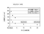
- FIG. 1 It is a schematic diagram which shows an example of the film-forming apparatus for enforcing the film-forming method of the metal film which concerns on one Embodiment of this invention. It is a timing chart which shows the sequence of the film-forming method of the metal film which concerns on one Embodiment of this invention. It is a figure which shows the relationship between the cycle number when process temperature is 160 degreeC, and the specific resistance of Ni film
- XRD X-ray diffraction
- FIG. 1 is a schematic view showing an example of a film forming apparatus for carrying out a metal film forming method according to an embodiment of the present invention.
- the film forming apparatus 100 has a substantially cylindrical chamber 1 that is hermetically configured, in which a susceptor 2 for horizontally supporting a wafer W that is a substrate to be processed is an exhaust chamber that will be described later. It is arrange
- the susceptor 2 is made of a ceramic such as AlN.
- a heater 5 is embedded in the susceptor 2, and a heater power source 6 is connected to the heater 5.
- a thermocouple 7 is provided in the vicinity of the upper surface of the susceptor 2, and a signal from the thermocouple 7 is transmitted to the heater controller 8.
- the heater controller 8 transmits a command to the heater power supply 6 in accordance with a signal from the thermocouple 7, and controls the heating of the heater 5 to control the wafer W to a predetermined temperature.
- an electrode 27 for applying high-frequency power is embedded.
- a high-frequency power source 29 is connected to the electrode 27 via a matching unit 28. If necessary, high-frequency power is applied to the electrode 27 to generate plasma, and plasma CVD can be performed.
- the susceptor 2 is provided with three wafer raising / lowering pins (not shown) so as to be able to project and retract with respect to the surface of the susceptor 2, and protrudes from the surface of the susceptor 2 when the wafer W is transferred. To be.
- a circular hole 1 b is formed in the top wall 1 a of the chamber 1, and a shower head 10 is fitted so as to protrude into the chamber 1 therefrom.
- the shower head 10 is for discharging a film-forming gas supplied from a gas supply mechanism 30 to be described later into the chamber 1.
- a gas supply mechanism 30 to be described later into the chamber 1.
- a first introduction path 11 is connected to the upper space 13, and a first gas discharge path 15 extends from the space 13 to the bottom surface of the shower head 10.
- a second introduction path 12 is connected to the lower space 14, and a second gas discharge path 16 extends from the space 14 to the bottom surface of the shower head 10. That is, the shower head 10 is configured to discharge Ni compound gas and NH 3 gas or H 2 gas as film forming materials independently from the discharge paths 15 and 16.
- An exhaust chamber 21 protruding downward is provided on the bottom wall of the chamber 1.
- An exhaust pipe 22 is connected to the side surface of the exhaust chamber 21, and an exhaust device 23 having a vacuum pump, a pressure control valve, and the like is connected to the exhaust pipe 22.
- an exhaust device 23 having a vacuum pump, a pressure control valve, and the like is connected to the exhaust pipe 22.
- a loading / unloading port 24 for loading / unloading the wafer W and a gate valve 25 for opening / closing the loading / unloading port 24 are provided on the side wall of the chamber 1.
- a heater 26 is provided on the wall portion of the chamber 1 so that the temperature of the inner wall of the chamber 1 can be controlled during the film forming process.
- the gas supply mechanism 30 stores a nickel amidate, for example, Ni (II) N, N′-di-tert-butylamidinate (Ni (II) (tBu-AMD) 2 ) as a film forming raw material.
- a raw material tank 31 is provided.
- a heater 31a is provided around the film forming material tank 31 so that the film forming material in the tank 31 can be heated to an appropriate temperature.
- Bubbling piping 32 for supplying Ar gas, which is a bubbling gas, from above is inserted into the film forming material tank 31 so as to be immersed in the film forming material.
- An Ar gas supply source 33 is connected to the bubbling pipe 32, and a mass flow controller 34 as a flow rate controller and front and rear valves 35 are interposed.
- a raw material gas delivery pipe 36 is inserted into the film forming raw material tank 31 from above, and the other end of the raw material gas delivery pipe 36 is connected to the first introduction path 11 of the shower head 10.
- a valve 37 is interposed in the source gas delivery pipe 36.
- the source gas delivery pipe 36 is provided with a heater 38 for preventing the deposition source gas from condensing.
- the film forming raw material is vaporized by bubbling in the film forming raw material tank 31, and the generated film forming raw material gas is supplied to the raw material gas delivery pipe 36 and the first gas supply pipe 36. 1 is supplied into the shower head 10 through one introduction path 11.
- Ar gas which is a bubbling gas
- the bubbling pipe 32 and the source gas delivery pipe 36 are connected by a bypass pipe 48, and a valve 49 is interposed in the bypass pipe 48.
- Valves 35a and 37a are interposed on the downstream side of the connecting portion of the bypass piping 48 in the bubbling piping 32 and the raw material gas delivery piping 36, respectively. Then, by closing the valves 35a and 37a and opening the valve 49, the argon gas from the Ar gas supply source 33 passes through the bubbling pipe 32, the bypass pipe 48, and the source gas delivery pipe 36 into the chamber 1 as a purge gas or the like. It is possible to supply.
- a pipe 40 is connected to the second introduction path 12 of the shower head 10, and a valve 41 is provided in the pipe 40.
- This pipe 40 is branched into branch pipes 40a and 40b.
- An NH 3 gas supply source 42 for introducing NH 3 gas as a reducing gas is connected to the branch pipe 40a, and an H 2 gas is connected to the branch pipe 40b.
- a supply source 43 is connected.
- the branch pipe 40a is provided with a mass flow controller 44 as a flow rate controller and a valve 45 before and after the mass flow controller 44
- the branch pipe 40b is provided with a mass flow controller 46 as a flow rate controller and a valve 47 before and after the mass flow controller 46.
- the reducing gas other NH 3, can be used hydrazine or, NH 3 derivatives, hydrazine derivatives.
- a branch pipe is further added to the pipe 40, and the mass flow controller and its front and rear are connected to this branch pipe. It is preferable to provide an Ar gas supply source for plasma ignition through a valve.
- This film forming apparatus has a control unit 50 that controls each component, specifically, a valve, a power source, a heater, a pump, and the like.
- the control unit 50 includes a process controller 51 including a microprocessor (computer), a user interface 52, and a storage unit 53.
- Each component of the film forming apparatus 100 is electrically connected to the process controller 51 and controlled.
- the user interface 52 is connected to the process controller 51 and visualizes the operation status of each component of the film forming apparatus and the keyboard on which the operator performs command input operations in order to manage each component of the film forming apparatus. It consists of a display that displays it.
- the storage unit 53 is also connected to the process controller 51, and the storage unit 53 corresponds to a control program for realizing various processes executed by the film forming apparatus 100 under the control of the process controller 51 and processing conditions.
- a control program for causing each component of the film forming apparatus 100 to execute a predetermined process, that is, a process recipe, various databases, and the like are stored.
- the processing recipe is stored in a storage medium (not shown) in the storage unit 53.
- the storage medium may be a fixed medium such as a hard disk or a portable medium such as a CDROM, DVD, or flash memory. Moreover, you may make it transmit a recipe suitably from another apparatus via a dedicated line, for example.
- a predetermined processing recipe is called from the storage unit 53 by an instruction from the user interface 52 and executed by the process controller 51, so that the film forming apparatus 100 can control the process controller 51. Desired processing is performed.
- the gate valve 25 is opened, and the wafer W is loaded into the chamber 1 through the loading / unloading port 24 by a transfer device (not shown) and placed on the susceptor 2.
- the inside of the chamber 1 is evacuated by the exhaust device 23 to bring the inside of the chamber 1 to a predetermined pressure, and the susceptor 2 is heated to a predetermined temperature.
- the denitrification step (Step 2) for desorbing is performed for one cycle, or two or more cycles are repeated with the purge step (Step 3) in between.
- nickel amidinate as a film forming raw material stored in the film forming raw material tank 31 for example, Ni (II) N, N′-di-tert-butylamidinate (Ni (II) ) (TBu-AMD) 2 ) is supplied with Ar gas as a bubbling gas, and Ni compound as a film forming raw material is vaporized by bubbling, and the raw material gas delivery pipe 36, the first introduction path 11, the shower head 10
- the NH 3 gas as a reducing gas is supplied from the NH 3 gas supply source 42 into the chamber 1 through the branch pipe 40 a, the pipe 40, the second introduction path 12, and the shower head 10. To do.
- reducing gas other NH 3
- reducing gas at least one selected from NH 3 , hydrazine, and derivatives thereof can be used.
- ammonia derivative for example, monomethylammonium can be used
- hydrazine derivative for example, monomethylhydrazine or dimethylhydrazine can be used. Of these, ammonia is preferred.
- the nickel amidinate used as a film-forming raw material is Ni (II) N, N′-di-tert-butylamidinate (Ni (II) (tBu-AMD) 2 ) as an example. ). That is, an amidinate ligand is bonded to Ni as a nucleus, and Ni substantially exists as Ni 2+ .
- a reducing agent having an unshared electron pair, such as NH 3 binds to the Ni nucleus present as Ni 2+ in the nickel amidinate of the above structure, and the amidinate ligand decomposes.
- this film formation reaction has good reactivity, low temperature film formation is possible, and the wafer temperature at that time is preferably 160 to 200 ° C.
- the wafer temperature at that time is preferably 160 to 200 ° C.
- the wafer temperature is lower than 160 ° C., the film formation reaction is slow, and a sufficient film formation rate cannot be obtained.
- it exceeds 200 degreeC there exists a possibility that a film
- the pressure in the chamber 1 is 133 to 665 Pa (1 to 5 Torr)
- the flow rate of Ar gas is 100 to 500 mL / min (sccm)
- the flow rate of NH 3 gas as a reducing gas is 400 to 4500 mL / min ( sccm).
- the thickness of the Ni film per film forming step is preferably 2 to 20 nm. This facilitates perform denitrification by H 2 gas in Step 2.
- the time for one film formation step is appropriately determined according to the film thickness of the film to be formed.
- a Ni film may be formed by plasma CVD by applying high frequency power from the high frequency power supply 29 to the electrode 27 in the susceptor 2 as necessary.
- Step 3 After the film formation process of Step 1 is completed, the purge process of Step 3 is performed.
- Step 3 after the valves 35a, 37a, 41, 45 are closed and the supply of the Ni compound gas and the NH 3 gas is stopped. While exhausting quickly by the exhaust device 23, the valve 49 is opened, and Ar gas is supplied into the chamber 1 through the bypass pipe 48 and the raw material gas delivery pipe 36 to purge the inside of the chamber 1.
- the Ar gas flow rate at this time is preferably 1000 to 5000 mL / min (sccm).
- the purge process time is preferably 5 to 20 sec.
- N remains as described above, and impurities such as O (oxygen) also remain. For this reason, the film as formed is high in specific resistance. Therefore, in the denitrification step (H 2 treatment) in Step 2, N is desorbed from the film formed in Step 1 by supplying H 2 gas. At this time, impurities such as O are also removed. For this reason, a Ni film having good film quality and low specific resistance can be obtained.
- H 2 treatment H 2 treatment
- the film formed in Step 1 has a structure in which a plurality of Ni atoms are surrounded by N atoms. For this reason, when the H 2 treatment is performed in-situ after purging after film formation, a reaction occurs in which H 2 gas supplied to the film becomes atomic H using Ni in the film as a catalyst. Since atomic H is extremely reactive, it can react with N in the film to quickly release N from the film. At this time, impurities such as O react with the atomic H and are quickly removed.
- N desorption from NixN is achieved by heating to about 300 ° C. without using H 2 treatment, but Ni aggregation occurs due to this heating, and a continuous film cannot be obtained. This is because Ni is forming a cluster near 300 ° C., and N has a structure of bonding to the Ni cluster, and Ni—Ni bonds are formed at the grain boundaries of the Ni cluster by the elimination of N. It is considered that each Ni cluster is separated because it becomes difficult.
- the H 2 treatment in Step 2 can sufficiently desorb N from the film even at a low temperature of 200 ° C. or lower, and can form a Ni film having a good surface state without causing Ni aggregation.
- the wafer W is kept heated by the susceptor 2 and Ar gas is allowed to flow into the chamber 1 at a flow rate of about 1000 to 3000 mL / min (sccm), or a valve With the valve 49 closed and the supply of Ar gas stopped, the valves 41 and 47 are opened to supply H 2 gas into the chamber 1.
- the flow rate of H 2 gas is preferably 1000 to 4000 mL / min (sccm).
- the higher the wafer temperature the higher the reactivity.
- the denitrification reaction proceeds sufficiently even at 200 ° C. or lower, and when the temperature is 200 ° C. or lower, film aggregation does not occur.
- the temperature is preferably 160 to 200 ° C. as in the film formation.
- the wafer temperature at this time is preferably set to the same temperature as that in the film forming process in Step 1.
- the heating temperature of the susceptor 2 can be made constant in a series of processes, and the throughput can be increased.
- the pressure in the chamber 1 is preferably 400 to 6000 Pa (3 to 45 Torr) in a state where the supply of Ar gas is stopped. Within the preferred temperature range and preferred pressure range of Step 2, higher temperatures and higher pressures are preferred.
- the time for the H 2 treatment in Step 2 is preferably 180 to 1200 seconds.
- the purge process in Step 3 may be performed to finish the film formation process.
- the effect of removing impurities can be further enhanced. That is, when a plurality of cycles are repeated in this way, denitrification is performed in an H 2 gas atmosphere after forming a thin Ni film, so that impurities can easily escape from the film.
- the greater the number of repetitions the higher the impurity removal effect and the lower the specific resistance.
- the number of repetitions is preferably 2 to 10 times, more preferably 4 to 10 times.
- the film thickness of one film formation is preferably 2 to 5 nm. Further, in order to effectively remove impurities from the film, it is preferable that the denitrification time in the H 2 gas atmosphere is long to some extent, but if it is too long, the throughput will be reduced. From such a viewpoint, as described above, the H 2 treatment time is preferably 180 to 1200 seconds.
- the gate valve 25 is opened, and the wafer W after film formation is unloaded through the loading / unloading port 24 by a transfer device (not shown).
- a wafer SiO 2 wafer
- a wafer Si wafer in which a 100-nm th-SiO 2 film (thermal oxide film) is formed on a 300 mm wafer silicon substrate
- a wafer Si wafer
- the surface of the silicon substrate is cleaned with dilute hydrofluoric acid
- film formation step 1) -purge (step 3) -H 2 treatment (step 2) -purge (step 3) is set as one cycle, and this is performed for a predetermined cycle.
- a Ni film having a predetermined thickness was formed.
- the pressure in the chamber is set to 665 Pa (5 Torr), and Ni (II) N, N′-di-tert-butylamidinate (Ni (II) (tBu-AMD) is used as a film forming raw material.
- 2 is stored in the film forming raw material tank 31, the temperature of the film forming raw material is maintained at 95 ° C. by the heater 31a, Ar gas is supplied at 100 mL / min (sccm), and Ni (II) (tBu ⁇ is supplied by bubbling.
- (AMD) 2 gas was supplied into the chamber, and NH 3 gas was supplied at a flow rate of 800 mL / min (sccm) from an NH 3 gas supply source, and a Ni film was formed by CVD.
- the pressure in the chamber was set to 400 Pa (3 Torr), and H 2 gas was supplied at 3000 mL / min (sccm).
- step 1 and step 2 were the same temperature in both processes.
- the number of cycles was 1, 2, 4, 10 and 20 and the target film thickness was 20 nm.
- the film formation time and target film thickness of Step 1 per time are 590 sec and 20 nm when the number of cycles is 1, 350 sec and 10 nm when the number of cycles is 2, and 210 sec and 5 nm when the number of cycles is 4, and 10 times when the number is 10 times 100 sec and 2 nm, and 20 times were 60 sec and 1 nm.
- the H 2 treatment time was 180 sec and 1200 sec up to 4 cycles, and only 1200 sec for 10 and 20 times.
- the number of cycles was 1, 2, and 4 and the target film thickness was also 20 nm.
- the film formation time and the target film thickness in Step 1 per time were 290 sec and 20 nm when the number of cycles was 1, and 175 sec and 10 nm when the number of cycles was 2, and 110 sec and 5 nm when the number of cycles was 4.
- the time for H 2 treatment was set to only 1200 seconds.
- FIG. 3A and 3B are diagrams showing the relationship between the number of cycles of the above process and the specific resistance of the obtained Ni film when the experiment was performed at 160 ° C.
- FIG. 3A shows the result of the Si chip
- FIG. Indicates the result of the SiO 2 wafer.
- the specific resistance decreases as the number of cycles increases, but it has been confirmed that the slope of the decrease becomes gentle around four cycles.
- the effect of reducing the specific resistance was greater when the time of H 2 treatment was 1200 seconds than 180 seconds.
- the specific resistance of 10 cycles was 34 ⁇ -cm and 20 times was 27 ⁇ -cm at 1200 sec for H 2 treatment, which was a low value.
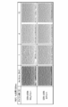
- FIG. 4 is an X-ray diffraction (XRD) chart of the Ni film (H 2 treatment time 1200 sec) formed at each cycle number when the experiment was performed at 160 ° C.
- the vertical axis indicates the intensity of the diffraction line in arbitrary units (au)
- the horizontal axis indicates the angle of the diffraction line
- the respective graphs are drawn while being shifted in the vertical direction so as not to overlap.
- the Ni 3 N peak is observed when the film is formed (as depo), but it was confirmed that the Ni 3 N peak disappeared by performing the H 2 treatment.
- FIG. 5 is an SEM photograph of the surface of the Ni film (H 2 treatment time 1200 sec) formed at the cycle number of 1, 4, and 10 when the experiment was performed at 160 ° C. From this SEM photograph, microcracks are observed on the surface of the film at a cycle number of 1, but when the number of cycles is 4 or 10, a finer and smoother film than as depo can be obtained. It was confirmed that it did not occur.
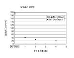
- FIG. 6A and 6B are diagrams showing the relationship between the number of cycles of the above process and the specific resistance of the obtained Ni film when the experiment was performed at 200 ° C.
- FIG. 6A shows the result of the Si wafer
- FIG. Indicates the result of the SiO 2 wafer.
- the specific resistance decreased as the number of cycles increased.
- the effect of lowering the specific resistance is greater than when the experiment was performed at 160 ° C., and reached a substantially saturated value at 2 cycles, 23.8 ⁇ -cm, and 40.6 at 20.6 ⁇ -cm, 160 ° C.
- the value was lower than 20 cycles. This is presumed to be because the impurities were reduced due to the increase in the temperature of Ni film formation and H 2 treatment.
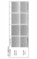
- FIG. 7 is an SEM photograph of the surface of the Ni film (H 2 treatment time 1200 sec) formed by the number of cycles 1, 2, and 4 when the experiment was performed at 200 ° C. From this SEM photograph, the surface state (morphology) of the film is very bad in as depo (especially on the Si chip), but the surface state of the film is slightly improved by one cycle and greatly improved by two cycles. A finely textured and very smooth surface was obtained with two or more cycles. Also, no microcracks are seen.
- FIG. 8 shows a case where the Ni film is formed on the SiO 2 film by changing the temperature and performing the film formation-purge-H 2 treatment (3 Torr, 180 sec) -purge cycle described above a predetermined number of times. It is a figure which shows the change of Ni peak intensity in X-ray diffraction (XRF). From this figure, a Ni peak appeared at 90 ° C. or higher, and it was confirmed that a temperature of 90 ° C. or higher was required for film formation. However, when the temperature is lower than 160 ° C., a sufficient film forming speed cannot be obtained, and the film forming temperature is preferably 160 ° C. or higher.
- the Ni film is formed on the SiO 2 film by changing the temperature to 160 ° C., 200 ° C., 300 ° C., and 400 ° C. and performing the above-described film formation-purge-H 2 treatment (3 Torr, 180 sec) for a predetermined cycle. It is a SEM photograph of the surface. From this figure, a slight microcrack was observed at 200 ° C., but this was not affected by repeated film formation, so it was confirmed that the surface state could be maintained well up to 200 ° C. However, remarkable aggregation occurred at 300 ° C. or higher, and it was confirmed that a continuous film could not be formed even if repeated film formation was performed. From these facts, it was confirmed that the film forming temperature and the H 2 treatment temperature are preferably 160 to 200 ° C.
- FIG. 10 is a diagram showing these relationships when the temperature and pressure are changed with the processing time on the horizontal axis and the amount of decrease in the specific resistance value Rs on the vertical axis. From this figure, it was confirmed that the specific resistance value Rs decreased at a processing time of 180 to 1200 sec at any temperature and pressure. It was also confirmed that the amount of decrease in the specific resistance value Rs tends to increase as the processing time increases.
- the treatment temperature was set at two levels of 160 ° C.
- the pressure was set at three levels of 0.15 Torr, 3 Torr, and 45 Torr.
- the decrease in specific resistance tends to increase at a temperature of 180 ° C.
- the pressure was good from 3 to 45 Torr, and that the treatment time and pressure were the highest at 180 ° C. and 45 Torr within the range of the experiment, the decrease amount of the specific resistance value Rs was the largest.
- Ni (II) (tBu-AMD) 2 is exemplified as the nickel amidinate as a film forming raw material, but other nickel amidinates may be used. .
- the structure of the film forming apparatus is not limited to that of the above embodiment, and the method for supplying the film forming raw material is not limited to the method of the above embodiment, and various methods can be applied.
Landscapes
- Chemical & Material Sciences (AREA)
- General Chemical & Material Sciences (AREA)
- Chemical Kinetics & Catalysis (AREA)
- Engineering & Computer Science (AREA)
- Materials Engineering (AREA)
- Mechanical Engineering (AREA)
- Metallurgy (AREA)
- Organic Chemistry (AREA)
- Chemical Vapour Deposition (AREA)
- Electrodes Of Semiconductors (AREA)
Abstract
Description
本実施形態では、金属膜としてニッケル膜を形成する場合について説明する。図1は、本発明の一実施形態に係る金属膜の成膜方法を実施するための成膜装置の一例を示す模式図である。
まず、ゲートバルブ25を開け、図示せぬ搬送装置によりウエハWを、搬入出口24を介してチャンバー1内に搬入し、サセプタ2上に載置する。次いで、チャンバー1内を排気装置23により排気してチャンバー1内を所定の圧力にし、サセプタ2を所定温度に加熱し、その状態で図2に示すように、成膜原料ガスであるニッケルアミジネートと還元ガスとを供給してNを含有するNi膜を成膜する成膜工程(ステップ1)と、成膜されたNを含有するNi膜にH2ガスを供給してその膜からNを脱離させる脱窒素工程(ステップ2)とを、パージ工程(ステップ3)を挟んで、1サイクル行うか、または2サイクル以上繰り返して行う。
成膜原料として用いるニッケルアミジネートは、Ni(II)N、N′-ジ-ターシャリブチルアミジネート(Ni(II)(tBu-AMD)2)を例にとると、以下の(1)式に示す構造を有している。

ステップ1において成膜された膜は、微視的にみると、N原子の周囲を複数のNi原子が取り囲んだ構造を有している。このため、成膜の後、パージに引き続き、in-situでH2処理を行うと、膜に供給されたH2ガスが膜中のNiを触媒として原子状Hとなる反応が生じる。原子状Hは極めて反応性が高いため、膜中のNと反応して膜中から速やかにNを離脱させることができる。この際に、O等の不純物も原子状Hと反応して速やかに除去される。
ここでは、300mmウエハのシリコン基板上に100nmのth-SiO2膜(熱酸化膜)を形成したウエハ(SiO2ウエハ)、およびシリコン基板の表面を希フッ酸洗浄したウエハ(Siウエハ)に対し、図1に示した成膜装置を用いて、成膜(ステップ1)-パージ(ステップ3)-H2処理(ステップ2)-パージ(ステップ3)を1サイクルとして、これを所定サイクル行って所定厚さのNi膜を成膜した。
Claims (8)
- 成膜原料としてニッケルアミジネートを用い、還元ガスとしてアンモニア、ヒドラジン、およびこれらの誘導体から選択された少なくとも1種を用いたCVDにより基板上に窒素を含むNi膜を成膜することと、
前記窒素を含むNi膜に水素ガスを供給して、Niを触媒として原子状水素を生成させ、生成した原子状水素により前記窒素を含むNi膜から窒素を脱離させることと
を含むサイクルを、1回または複数回行う、Ni膜の成膜方法。 - 前記窒素を含むNi膜を成膜することと、前記前記窒素を含むNi膜から窒素を脱離させることとは、パージ工程を挟んで1サイクルまたは複数サイクル行う、請求項1に記載のNi膜の成膜方法。
- 前記サイクルの回数は2~10回である、請求項1に記載のNi膜の成膜方法。
- 前記窒素を含むNi膜を成膜することと、前記窒素を含むNi膜から窒素を脱離させることとは、同じ温度で行われる、請求項1に記載のNi膜の成膜方法。
- 前記窒素を含むNi膜を成膜することと、前記窒素を含むNi膜から窒素を脱離させることとは、160~200℃で行なわれる、請求項4に記載のNi膜の成膜方法。
- 前記窒素を含むNi膜から窒素を脱離させることを実施する時間は、180~1200secである、請求項1に記載のNi膜の成膜方法。
- 前記窒素を含むNi膜から窒素を脱離させることを実施する際の圧力は、3~45Torrである、請求項1に記載のNi膜の成膜方法。
- コンピュータ上で動作し、成膜装置を制御するためのプログラムが記憶された記憶媒体であって、前記プログラムは、実行時に、成膜原料としてニッケルアミジネートを用い、還元ガスとしてアンモニア、ヒドラジン、およびこれらの誘導体から選択された少なくとも1種を用いたCVDにより基板上に窒素を含むNi膜を成膜することと、前記窒素を含むNi膜に水素ガスを供給して、Niを触媒として原子状水素を生成させ、生成した原子状水素により前記窒素を含むNi膜から窒素を脱離させることとを含むサイクルを、1回または複数回行う、Ni膜の成膜方法が行われるように、コンピュータに前記成膜装置を制御させる記憶媒体。
Priority Applications (3)
| Application Number | Priority Date | Filing Date | Title |
|---|---|---|---|
| CN2010800174183A CN102405304A (zh) | 2009-09-29 | 2010-09-28 | Ni膜的成膜方法 |
| US13/498,446 US20120183689A1 (en) | 2009-09-29 | 2010-09-28 | Ni film forming method |
| JP2011534238A JPWO2011040385A1 (ja) | 2009-09-29 | 2010-09-28 | Ni膜の成膜方法 |
Applications Claiming Priority (2)
| Application Number | Priority Date | Filing Date | Title |
|---|---|---|---|
| JP2009-223888 | 2009-09-29 | ||
| JP2009223888 | 2009-09-29 |
Publications (1)
| Publication Number | Publication Date |
|---|---|
| WO2011040385A1 true WO2011040385A1 (ja) | 2011-04-07 |
Family
ID=43826200
Family Applications (1)
| Application Number | Title | Priority Date | Filing Date |
|---|---|---|---|
| PCT/JP2010/066764 Ceased WO2011040385A1 (ja) | 2009-09-29 | 2010-09-28 | Ni膜の成膜方法 |
Country Status (6)
| Country | Link |
|---|---|
| US (1) | US20120183689A1 (ja) |
| JP (1) | JPWO2011040385A1 (ja) |
| KR (1) | KR20120062915A (ja) |
| CN (1) | CN102405304A (ja) |
| TW (1) | TW201131005A (ja) |
| WO (1) | WO2011040385A1 (ja) |
Cited By (9)
| Publication number | Priority date | Publication date | Assignee | Title |
|---|---|---|---|---|
| JP2013053337A (ja) * | 2011-09-02 | 2013-03-21 | Tokyo Electron Ltd | ニッケル膜の成膜方法 |
| WO2013051670A1 (ja) * | 2011-10-07 | 2013-04-11 | 気相成長株式会社 | コバルト系膜形成方法、コバルト系膜形成材料、及び新規化合物 |
| JP2013104100A (ja) * | 2011-11-14 | 2013-05-30 | Taiyo Nippon Sanso Corp | 金属薄膜の成膜方法および金属薄膜成膜用原料 |
| KR101363222B1 (ko) * | 2011-04-13 | 2014-02-12 | 가부시키가이샤 알박 | Ni 막의 형성 방법 |
| KR20140038328A (ko) | 2012-09-20 | 2014-03-28 | 도쿄엘렉트론가부시키가이샤 | 금속막의 성막 방법 |
| JP2015021175A (ja) * | 2013-07-19 | 2015-02-02 | 大陽日酸株式会社 | 金属薄膜の製膜方法 |
| WO2015049989A1 (ja) | 2013-10-02 | 2015-04-09 | 田中貴金属工業株式会社 | 化学蒸着法によるSi基板上へのニッケル薄膜、及び、Si基板上へのNiシリサイド薄膜の製造方法 |
| JP2015101752A (ja) * | 2013-11-25 | 2015-06-04 | 東京エレクトロン株式会社 | 金属膜の成膜方法 |
| JP2020502361A (ja) * | 2016-12-15 | 2020-01-23 | アーエスエム・イーぺー・ホールディング・ベスローテン・フェンノートシャップ | 逐次浸透合成装置 |
Families Citing this family (369)
| Publication number | Priority date | Publication date | Assignee | Title |
|---|---|---|---|---|
| US10378106B2 (en) | 2008-11-14 | 2019-08-13 | Asm Ip Holding B.V. | Method of forming insulation film by modified PEALD |
| US9394608B2 (en) | 2009-04-06 | 2016-07-19 | Asm America, Inc. | Semiconductor processing reactor and components thereof |
| US8802201B2 (en) | 2009-08-14 | 2014-08-12 | Asm America, Inc. | Systems and methods for thin-film deposition of metal oxides using excited nitrogen-oxygen species |
| US9312155B2 (en) | 2011-06-06 | 2016-04-12 | Asm Japan K.K. | High-throughput semiconductor-processing apparatus equipped with multiple dual-chamber modules |
| US10364496B2 (en) | 2011-06-27 | 2019-07-30 | Asm Ip Holding B.V. | Dual section module having shared and unshared mass flow controllers |
| US10854498B2 (en) | 2011-07-15 | 2020-12-01 | Asm Ip Holding B.V. | Wafer-supporting device and method for producing same |
| US20130023129A1 (en) | 2011-07-20 | 2013-01-24 | Asm America, Inc. | Pressure transmitter for a semiconductor processing environment |
| US9017481B1 (en) | 2011-10-28 | 2015-04-28 | Asm America, Inc. | Process feed management for semiconductor substrate processing |
| US9659799B2 (en) | 2012-08-28 | 2017-05-23 | Asm Ip Holding B.V. | Systems and methods for dynamic semiconductor process scheduling |
| US10714315B2 (en) | 2012-10-12 | 2020-07-14 | Asm Ip Holdings B.V. | Semiconductor reaction chamber showerhead |
| US20160376700A1 (en) | 2013-02-01 | 2016-12-29 | Asm Ip Holding B.V. | System for treatment of deposition reactor |
| US9484191B2 (en) | 2013-03-08 | 2016-11-01 | Asm Ip Holding B.V. | Pulsed remote plasma method and system |
| US9589770B2 (en) | 2013-03-08 | 2017-03-07 | Asm Ip Holding B.V. | Method and systems for in-situ formation of intermediate reactive species |
| US9240412B2 (en) | 2013-09-27 | 2016-01-19 | Asm Ip Holding B.V. | Semiconductor structure and device and methods of forming same using selective epitaxial process |
| KR102198856B1 (ko) | 2014-02-10 | 2021-01-05 | 삼성전자 주식회사 | 니켈 함유막을 포함하는 반도체 소자의 제조 방법 |
| US10683571B2 (en) | 2014-02-25 | 2020-06-16 | Asm Ip Holding B.V. | Gas supply manifold and method of supplying gases to chamber using same |
| US10167557B2 (en) | 2014-03-18 | 2019-01-01 | Asm Ip Holding B.V. | Gas distribution system, reactor including the system, and methods of using the same |
| KR102168174B1 (ko) | 2014-03-19 | 2020-10-20 | 삼성전자주식회사 | 니켈 화합물 및 이를 이용한 박막 형성 방법 |
| US11015245B2 (en) | 2014-03-19 | 2021-05-25 | Asm Ip Holding B.V. | Gas-phase reactor and system having exhaust plenum and components thereof |
| US10858737B2 (en) | 2014-07-28 | 2020-12-08 | Asm Ip Holding B.V. | Showerhead assembly and components thereof |
| US9890456B2 (en) | 2014-08-21 | 2018-02-13 | Asm Ip Holding B.V. | Method and system for in situ formation of gas-phase compounds |
| US10941490B2 (en) | 2014-10-07 | 2021-03-09 | Asm Ip Holding B.V. | Multiple temperature range susceptor, assembly, reactor and system including the susceptor, and methods of using the same |
| US9657845B2 (en) | 2014-10-07 | 2017-05-23 | Asm Ip Holding B.V. | Variable conductance gas distribution apparatus and method |
| US10100407B2 (en) * | 2014-12-19 | 2018-10-16 | Lam Research Corporation | Hardware and process for film uniformity improvement |
| KR102263121B1 (ko) | 2014-12-22 | 2021-06-09 | 에이에스엠 아이피 홀딩 비.브이. | 반도체 소자 및 그 제조 방법 |
| US10529542B2 (en) | 2015-03-11 | 2020-01-07 | Asm Ip Holdings B.V. | Cross-flow reactor and method |
| US10276355B2 (en) | 2015-03-12 | 2019-04-30 | Asm Ip Holding B.V. | Multi-zone reactor, system including the reactor, and method of using the same |
| US10458018B2 (en) | 2015-06-26 | 2019-10-29 | Asm Ip Holding B.V. | Structures including metal carbide material, devices including the structures, and methods of forming same |
| US10600673B2 (en) | 2015-07-07 | 2020-03-24 | Asm Ip Holding B.V. | Magnetic susceptor to baseplate seal |
| US9960072B2 (en) | 2015-09-29 | 2018-05-01 | Asm Ip Holding B.V. | Variable adjustment for precise matching of multiple chamber cavity housings |
| US10211308B2 (en) | 2015-10-21 | 2019-02-19 | Asm Ip Holding B.V. | NbMC layers |
| US10322384B2 (en) | 2015-11-09 | 2019-06-18 | Asm Ip Holding B.V. | Counter flow mixer for process chamber |
| US11139308B2 (en) | 2015-12-29 | 2021-10-05 | Asm Ip Holding B.V. | Atomic layer deposition of III-V compounds to form V-NAND devices |
| US10468251B2 (en) | 2016-02-19 | 2019-11-05 | Asm Ip Holding B.V. | Method for forming spacers using silicon nitride film for spacer-defined multiple patterning |
| US10529554B2 (en) | 2016-02-19 | 2020-01-07 | Asm Ip Holding B.V. | Method for forming silicon nitride film selectively on sidewalls or flat surfaces of trenches |
| US10501866B2 (en) | 2016-03-09 | 2019-12-10 | Asm Ip Holding B.V. | Gas distribution apparatus for improved film uniformity in an epitaxial system |
| US10343920B2 (en) | 2016-03-18 | 2019-07-09 | Asm Ip Holding B.V. | Aligned carbon nanotubes |
| US9892913B2 (en) | 2016-03-24 | 2018-02-13 | Asm Ip Holding B.V. | Radial and thickness control via biased multi-port injection settings |
| US10865475B2 (en) | 2016-04-21 | 2020-12-15 | Asm Ip Holding B.V. | Deposition of metal borides and silicides |
| US10190213B2 (en) | 2016-04-21 | 2019-01-29 | Asm Ip Holding B.V. | Deposition of metal borides |
| US10032628B2 (en) | 2016-05-02 | 2018-07-24 | Asm Ip Holding B.V. | Source/drain performance through conformal solid state doping |
| US10367080B2 (en) | 2016-05-02 | 2019-07-30 | Asm Ip Holding B.V. | Method of forming a germanium oxynitride film |
| KR102592471B1 (ko) | 2016-05-17 | 2023-10-20 | 에이에스엠 아이피 홀딩 비.브이. | 금속 배선 형성 방법 및 이를 이용한 반도체 장치의 제조 방법 |
| US11453943B2 (en) | 2016-05-25 | 2022-09-27 | Asm Ip Holding B.V. | Method for forming carbon-containing silicon/metal oxide or nitride film by ALD using silicon precursor and hydrocarbon precursor |
| US10388509B2 (en) | 2016-06-28 | 2019-08-20 | Asm Ip Holding B.V. | Formation of epitaxial layers via dislocation filtering |
| US9859151B1 (en) | 2016-07-08 | 2018-01-02 | Asm Ip Holding B.V. | Selective film deposition method to form air gaps |
| US10612137B2 (en) | 2016-07-08 | 2020-04-07 | Asm Ip Holdings B.V. | Organic reactants for atomic layer deposition |
| US10714385B2 (en) | 2016-07-19 | 2020-07-14 | Asm Ip Holding B.V. | Selective deposition of tungsten |
| US10381226B2 (en) | 2016-07-27 | 2019-08-13 | Asm Ip Holding B.V. | Method of processing substrate |
| US9887082B1 (en) | 2016-07-28 | 2018-02-06 | Asm Ip Holding B.V. | Method and apparatus for filling a gap |
| US9812320B1 (en) | 2016-07-28 | 2017-11-07 | Asm Ip Holding B.V. | Method and apparatus for filling a gap |
| KR102532607B1 (ko) | 2016-07-28 | 2023-05-15 | 에이에스엠 아이피 홀딩 비.브이. | 기판 가공 장치 및 그 동작 방법 |
| US10395919B2 (en) | 2016-07-28 | 2019-08-27 | Asm Ip Holding B.V. | Method and apparatus for filling a gap |
| KR102613349B1 (ko) | 2016-08-25 | 2023-12-14 | 에이에스엠 아이피 홀딩 비.브이. | 배기 장치 및 이를 이용한 기판 가공 장치와 박막 제조 방법 |
| US10410943B2 (en) | 2016-10-13 | 2019-09-10 | Asm Ip Holding B.V. | Method for passivating a surface of a semiconductor and related systems |
| US10643826B2 (en) | 2016-10-26 | 2020-05-05 | Asm Ip Holdings B.V. | Methods for thermally calibrating reaction chambers |
| US11532757B2 (en) | 2016-10-27 | 2022-12-20 | Asm Ip Holding B.V. | Deposition of charge trapping layers |
| US10229833B2 (en) | 2016-11-01 | 2019-03-12 | Asm Ip Holding B.V. | Methods for forming a transition metal nitride film on a substrate by atomic layer deposition and related semiconductor device structures |
| US10714350B2 (en) | 2016-11-01 | 2020-07-14 | ASM IP Holdings, B.V. | Methods for forming a transition metal niobium nitride film on a substrate by atomic layer deposition and related semiconductor device structures |
| US10435790B2 (en) | 2016-11-01 | 2019-10-08 | Asm Ip Holding B.V. | Method of subatmospheric plasma-enhanced ALD using capacitively coupled electrodes with narrow gap |
| US10643904B2 (en) | 2016-11-01 | 2020-05-05 | Asm Ip Holdings B.V. | Methods for forming a semiconductor device and related semiconductor device structures |
| US10134757B2 (en) | 2016-11-07 | 2018-11-20 | Asm Ip Holding B.V. | Method of processing a substrate and a device manufactured by using the method |
| KR102546317B1 (ko) | 2016-11-15 | 2023-06-21 | 에이에스엠 아이피 홀딩 비.브이. | 기체 공급 유닛 및 이를 포함하는 기판 처리 장치 |
| US10340135B2 (en) | 2016-11-28 | 2019-07-02 | Asm Ip Holding B.V. | Method of topologically restricted plasma-enhanced cyclic deposition of silicon or metal nitride |
| KR102762543B1 (ko) | 2016-12-14 | 2025-02-05 | 에이에스엠 아이피 홀딩 비.브이. | 기판 처리 장치 |
| US11447861B2 (en) | 2016-12-15 | 2022-09-20 | Asm Ip Holding B.V. | Sequential infiltration synthesis apparatus and a method of forming a patterned structure |
| KR102700194B1 (ko) | 2016-12-19 | 2024-08-28 | 에이에스엠 아이피 홀딩 비.브이. | 기판 처리 장치 |
| US10269558B2 (en) | 2016-12-22 | 2019-04-23 | Asm Ip Holding B.V. | Method of forming a structure on a substrate |
| US10867788B2 (en) | 2016-12-28 | 2020-12-15 | Asm Ip Holding B.V. | Method of forming a structure on a substrate |
| US11390950B2 (en) | 2017-01-10 | 2022-07-19 | Asm Ip Holding B.V. | Reactor system and method to reduce residue buildup during a film deposition process |
| US10655221B2 (en) | 2017-02-09 | 2020-05-19 | Asm Ip Holding B.V. | Method for depositing oxide film by thermal ALD and PEALD |
| US10468261B2 (en) | 2017-02-15 | 2019-11-05 | Asm Ip Holding B.V. | Methods for forming a metallic film on a substrate by cyclical deposition and related semiconductor device structures |
| US10283353B2 (en) | 2017-03-29 | 2019-05-07 | Asm Ip Holding B.V. | Method of reforming insulating film deposited on substrate with recess pattern |
| US10529563B2 (en) | 2017-03-29 | 2020-01-07 | Asm Ip Holdings B.V. | Method for forming doped metal oxide films on a substrate by cyclical deposition and related semiconductor device structures |
| KR102457289B1 (ko) | 2017-04-25 | 2022-10-21 | 에이에스엠 아이피 홀딩 비.브이. | 박막 증착 방법 및 반도체 장치의 제조 방법 |
| US10770286B2 (en) | 2017-05-08 | 2020-09-08 | Asm Ip Holdings B.V. | Methods for selectively forming a silicon nitride film on a substrate and related semiconductor device structures |
| US10892156B2 (en) | 2017-05-08 | 2021-01-12 | Asm Ip Holding B.V. | Methods for forming a silicon nitride film on a substrate and related semiconductor device structures |
| US10446393B2 (en) | 2017-05-08 | 2019-10-15 | Asm Ip Holding B.V. | Methods for forming silicon-containing epitaxial layers and related semiconductor device structures |
| US10504742B2 (en) | 2017-05-31 | 2019-12-10 | Asm Ip Holding B.V. | Method of atomic layer etching using hydrogen plasma |
| US10886123B2 (en) | 2017-06-02 | 2021-01-05 | Asm Ip Holding B.V. | Methods for forming low temperature semiconductor layers and related semiconductor device structures |
| US12040200B2 (en) | 2017-06-20 | 2024-07-16 | Asm Ip Holding B.V. | Semiconductor processing apparatus and methods for calibrating a semiconductor processing apparatus |
| US11306395B2 (en) | 2017-06-28 | 2022-04-19 | Asm Ip Holding B.V. | Methods for depositing a transition metal nitride film on a substrate by atomic layer deposition and related deposition apparatus |
| US10685834B2 (en) | 2017-07-05 | 2020-06-16 | Asm Ip Holdings B.V. | Methods for forming a silicon germanium tin layer and related semiconductor device structures |
| KR20190009245A (ko) | 2017-07-18 | 2019-01-28 | 에이에스엠 아이피 홀딩 비.브이. | 반도체 소자 구조물 형성 방법 및 관련된 반도체 소자 구조물 |
| US11374112B2 (en) | 2017-07-19 | 2022-06-28 | Asm Ip Holding B.V. | Method for depositing a group IV semiconductor and related semiconductor device structures |
| US10541333B2 (en) | 2017-07-19 | 2020-01-21 | Asm Ip Holding B.V. | Method for depositing a group IV semiconductor and related semiconductor device structures |
| US11018002B2 (en) | 2017-07-19 | 2021-05-25 | Asm Ip Holding B.V. | Method for selectively depositing a Group IV semiconductor and related semiconductor device structures |
| US10312055B2 (en) | 2017-07-26 | 2019-06-04 | Asm Ip Holding B.V. | Method of depositing film by PEALD using negative bias |
| US10605530B2 (en) | 2017-07-26 | 2020-03-31 | Asm Ip Holding B.V. | Assembly of a liner and a flange for a vertical furnace as well as the liner and the vertical furnace |
| US10590535B2 (en) | 2017-07-26 | 2020-03-17 | Asm Ip Holdings B.V. | Chemical treatment, deposition and/or infiltration apparatus and method for using the same |
| TWI815813B (zh) | 2017-08-04 | 2023-09-21 | 荷蘭商Asm智慧財產控股公司 | 用於分配反應腔內氣體的噴頭總成 |
| US10770336B2 (en) | 2017-08-08 | 2020-09-08 | Asm Ip Holding B.V. | Substrate lift mechanism and reactor including same |
| US10692741B2 (en) | 2017-08-08 | 2020-06-23 | Asm Ip Holdings B.V. | Radiation shield |
| US10249524B2 (en) | 2017-08-09 | 2019-04-02 | Asm Ip Holding B.V. | Cassette holder assembly for a substrate cassette and holding member for use in such assembly |
| US11139191B2 (en) | 2017-08-09 | 2021-10-05 | Asm Ip Holding B.V. | Storage apparatus for storing cassettes for substrates and processing apparatus equipped therewith |
| US11769682B2 (en) | 2017-08-09 | 2023-09-26 | Asm Ip Holding B.V. | Storage apparatus for storing cassettes for substrates and processing apparatus equipped therewith |
| USD900036S1 (en) | 2017-08-24 | 2020-10-27 | Asm Ip Holding B.V. | Heater electrical connector and adapter |
| US11830730B2 (en) | 2017-08-29 | 2023-11-28 | Asm Ip Holding B.V. | Layer forming method and apparatus |
| US11056344B2 (en) | 2017-08-30 | 2021-07-06 | Asm Ip Holding B.V. | Layer forming method |
| US11295980B2 (en) | 2017-08-30 | 2022-04-05 | Asm Ip Holding B.V. | Methods for depositing a molybdenum metal film over a dielectric surface of a substrate by a cyclical deposition process and related semiconductor device structures |
| KR102491945B1 (ko) | 2017-08-30 | 2023-01-26 | 에이에스엠 아이피 홀딩 비.브이. | 기판 처리 장치 |
| KR102401446B1 (ko) | 2017-08-31 | 2022-05-24 | 에이에스엠 아이피 홀딩 비.브이. | 기판 처리 장치 |
| US10607895B2 (en) | 2017-09-18 | 2020-03-31 | Asm Ip Holdings B.V. | Method for forming a semiconductor device structure comprising a gate fill metal |
| KR102630301B1 (ko) | 2017-09-21 | 2024-01-29 | 에이에스엠 아이피 홀딩 비.브이. | 침투성 재료의 순차 침투 합성 방법 처리 및 이를 이용하여 형성된 구조물 및 장치 |
| US10844484B2 (en) | 2017-09-22 | 2020-11-24 | Asm Ip Holding B.V. | Apparatus for dispensing a vapor phase reactant to a reaction chamber and related methods |
| US10658205B2 (en) | 2017-09-28 | 2020-05-19 | Asm Ip Holdings B.V. | Chemical dispensing apparatus and methods for dispensing a chemical to a reaction chamber |
| US10403504B2 (en) | 2017-10-05 | 2019-09-03 | Asm Ip Holding B.V. | Method for selectively depositing a metallic film on a substrate |
| US10319588B2 (en) | 2017-10-10 | 2019-06-11 | Asm Ip Holding B.V. | Method for depositing a metal chalcogenide on a substrate by cyclical deposition |
| US10923344B2 (en) | 2017-10-30 | 2021-02-16 | Asm Ip Holding B.V. | Methods for forming a semiconductor structure and related semiconductor structures |
| KR102443047B1 (ko) | 2017-11-16 | 2022-09-14 | 에이에스엠 아이피 홀딩 비.브이. | 기판 처리 장치 방법 및 그에 의해 제조된 장치 |
| US10910262B2 (en) | 2017-11-16 | 2021-02-02 | Asm Ip Holding B.V. | Method of selectively depositing a capping layer structure on a semiconductor device structure |
| US11022879B2 (en) | 2017-11-24 | 2021-06-01 | Asm Ip Holding B.V. | Method of forming an enhanced unexposed photoresist layer |
| JP7214724B2 (ja) | 2017-11-27 | 2023-01-30 | エーエスエム アイピー ホールディング ビー.ブイ. | バッチ炉で利用されるウェハカセットを収納するための収納装置 |
| TWI791689B (zh) | 2017-11-27 | 2023-02-11 | 荷蘭商Asm智慧財產控股私人有限公司 | 包括潔淨迷你環境之裝置 |
| US10290508B1 (en) | 2017-12-05 | 2019-05-14 | Asm Ip Holding B.V. | Method for forming vertical spacers for spacer-defined patterning |
| US10872771B2 (en) | 2018-01-16 | 2020-12-22 | Asm Ip Holding B. V. | Method for depositing a material film on a substrate within a reaction chamber by a cyclical deposition process and related device structures |
| KR102695659B1 (ko) | 2018-01-19 | 2024-08-14 | 에이에스엠 아이피 홀딩 비.브이. | 플라즈마 보조 증착에 의해 갭 충진 층을 증착하는 방법 |
| TWI799494B (zh) | 2018-01-19 | 2023-04-21 | 荷蘭商Asm 智慧財產控股公司 | 沈積方法 |
| USD903477S1 (en) | 2018-01-24 | 2020-12-01 | Asm Ip Holdings B.V. | Metal clamp |
| US11018047B2 (en) | 2018-01-25 | 2021-05-25 | Asm Ip Holding B.V. | Hybrid lift pin |
| US10535516B2 (en) | 2018-02-01 | 2020-01-14 | Asm Ip Holdings B.V. | Method for depositing a semiconductor structure on a surface of a substrate and related semiconductor structures |
| USD880437S1 (en) | 2018-02-01 | 2020-04-07 | Asm Ip Holding B.V. | Gas supply plate for semiconductor manufacturing apparatus |
| US11081345B2 (en) | 2018-02-06 | 2021-08-03 | Asm Ip Holding B.V. | Method of post-deposition treatment for silicon oxide film |
| US11685991B2 (en) | 2018-02-14 | 2023-06-27 | Asm Ip Holding B.V. | Method for depositing a ruthenium-containing film on a substrate by a cyclical deposition process |
| US10896820B2 (en) | 2018-02-14 | 2021-01-19 | Asm Ip Holding B.V. | Method for depositing a ruthenium-containing film on a substrate by a cyclical deposition process |
| US10731249B2 (en) | 2018-02-15 | 2020-08-04 | Asm Ip Holding B.V. | Method of forming a transition metal containing film on a substrate by a cyclical deposition process, a method for supplying a transition metal halide compound to a reaction chamber, and related vapor deposition apparatus |
| KR102636427B1 (ko) | 2018-02-20 | 2024-02-13 | 에이에스엠 아이피 홀딩 비.브이. | 기판 처리 방법 및 장치 |
| US10658181B2 (en) | 2018-02-20 | 2020-05-19 | Asm Ip Holding B.V. | Method of spacer-defined direct patterning in semiconductor fabrication |
| US10975470B2 (en) | 2018-02-23 | 2021-04-13 | Asm Ip Holding B.V. | Apparatus for detecting or monitoring for a chemical precursor in a high temperature environment |
| US11473195B2 (en) | 2018-03-01 | 2022-10-18 | Asm Ip Holding B.V. | Semiconductor processing apparatus and a method for processing a substrate |
| US11629406B2 (en) | 2018-03-09 | 2023-04-18 | Asm Ip Holding B.V. | Semiconductor processing apparatus comprising one or more pyrometers for measuring a temperature of a substrate during transfer of the substrate |
| US11114283B2 (en) | 2018-03-16 | 2021-09-07 | Asm Ip Holding B.V. | Reactor, system including the reactor, and methods of manufacturing and using same |
| KR102646467B1 (ko) | 2018-03-27 | 2024-03-11 | 에이에스엠 아이피 홀딩 비.브이. | 기판 상에 전극을 형성하는 방법 및 전극을 포함하는 반도체 소자 구조 |
| US11230766B2 (en) | 2018-03-29 | 2022-01-25 | Asm Ip Holding B.V. | Substrate processing apparatus and method |
| US10510536B2 (en) | 2018-03-29 | 2019-12-17 | Asm Ip Holding B.V. | Method of depositing a co-doped polysilicon film on a surface of a substrate within a reaction chamber |
| US11088002B2 (en) | 2018-03-29 | 2021-08-10 | Asm Ip Holding B.V. | Substrate rack and a substrate processing system and method |
| KR102501472B1 (ko) | 2018-03-30 | 2023-02-20 | 에이에스엠 아이피 홀딩 비.브이. | 기판 처리 방법 |
| KR102600229B1 (ko) | 2018-04-09 | 2023-11-10 | 에이에스엠 아이피 홀딩 비.브이. | 기판 지지 장치, 이를 포함하는 기판 처리 장치 및 기판 처리 방법 |
| TWI843623B (zh) | 2018-05-08 | 2024-05-21 | 荷蘭商Asm Ip私人控股有限公司 | 藉由循環沉積製程於基板上沉積氧化物膜之方法及相關裝置結構 |
| US12025484B2 (en) | 2018-05-08 | 2024-07-02 | Asm Ip Holding B.V. | Thin film forming method |
| US12272527B2 (en) | 2018-05-09 | 2025-04-08 | Asm Ip Holding B.V. | Apparatus for use with hydrogen radicals and method of using same |
| KR20190129718A (ko) | 2018-05-11 | 2019-11-20 | 에이에스엠 아이피 홀딩 비.브이. | 기판 상에 피도핑 금속 탄화물 막을 형성하는 방법 및 관련 반도체 소자 구조 |
| KR102596988B1 (ko) | 2018-05-28 | 2023-10-31 | 에이에스엠 아이피 홀딩 비.브이. | 기판 처리 방법 및 그에 의해 제조된 장치 |
| US11718913B2 (en) | 2018-06-04 | 2023-08-08 | Asm Ip Holding B.V. | Gas distribution system and reactor system including same |
| TWI840362B (zh) | 2018-06-04 | 2024-05-01 | 荷蘭商Asm Ip私人控股有限公司 | 水氣降低的晶圓處置腔室 |
| US11286562B2 (en) | 2018-06-08 | 2022-03-29 | Asm Ip Holding B.V. | Gas-phase chemical reactor and method of using same |
| KR102568797B1 (ko) | 2018-06-21 | 2023-08-21 | 에이에스엠 아이피 홀딩 비.브이. | 기판 처리 시스템 |
| US10797133B2 (en) | 2018-06-21 | 2020-10-06 | Asm Ip Holding B.V. | Method for depositing a phosphorus doped silicon arsenide film and related semiconductor device structures |
| TWI871083B (zh) | 2018-06-27 | 2025-01-21 | 荷蘭商Asm Ip私人控股有限公司 | 用於形成含金屬材料之循環沉積製程 |
| US11499222B2 (en) | 2018-06-27 | 2022-11-15 | Asm Ip Holding B.V. | Cyclic deposition methods for forming metal-containing material and films and structures including the metal-containing material |
| KR102686758B1 (ko) | 2018-06-29 | 2024-07-18 | 에이에스엠 아이피 홀딩 비.브이. | 박막 증착 방법 및 반도체 장치의 제조 방법 |
| US10612136B2 (en) | 2018-06-29 | 2020-04-07 | ASM IP Holding, B.V. | Temperature-controlled flange and reactor system including same |
| US10755922B2 (en) | 2018-07-03 | 2020-08-25 | Asm Ip Holding B.V. | Method for depositing silicon-free carbon-containing film as gap-fill layer by pulse plasma-assisted deposition |
| US10388513B1 (en) | 2018-07-03 | 2019-08-20 | Asm Ip Holding B.V. | Method for depositing silicon-free carbon-containing film as gap-fill layer by pulse plasma-assisted deposition |
| US10767789B2 (en) | 2018-07-16 | 2020-09-08 | Asm Ip Holding B.V. | Diaphragm valves, valve components, and methods for forming valve components |
| US10483099B1 (en) | 2018-07-26 | 2019-11-19 | Asm Ip Holding B.V. | Method for forming thermally stable organosilicon polymer film |
| US11053591B2 (en) | 2018-08-06 | 2021-07-06 | Asm Ip Holding B.V. | Multi-port gas injection system and reactor system including same |
| US10883175B2 (en) | 2018-08-09 | 2021-01-05 | Asm Ip Holding B.V. | Vertical furnace for processing substrates and a liner for use therein |
| US10829852B2 (en) | 2018-08-16 | 2020-11-10 | Asm Ip Holding B.V. | Gas distribution device for a wafer processing apparatus |
| US11430674B2 (en) | 2018-08-22 | 2022-08-30 | Asm Ip Holding B.V. | Sensor array, apparatus for dispensing a vapor phase reactant to a reaction chamber and related methods |
| KR102707956B1 (ko) | 2018-09-11 | 2024-09-19 | 에이에스엠 아이피 홀딩 비.브이. | 박막 증착 방법 |
| US11024523B2 (en) | 2018-09-11 | 2021-06-01 | Asm Ip Holding B.V. | Substrate processing apparatus and method |
| US11049751B2 (en) | 2018-09-14 | 2021-06-29 | Asm Ip Holding B.V. | Cassette supply system to store and handle cassettes and processing apparatus equipped therewith |
| CN110970344B (zh) | 2018-10-01 | 2024-10-25 | Asmip控股有限公司 | 衬底保持设备、包含所述设备的系统及其使用方法 |
| US11232963B2 (en) | 2018-10-03 | 2022-01-25 | Asm Ip Holding B.V. | Substrate processing apparatus and method |
| KR102592699B1 (ko) | 2018-10-08 | 2023-10-23 | 에이에스엠 아이피 홀딩 비.브이. | 기판 지지 유닛 및 이를 포함하는 박막 증착 장치와 기판 처리 장치 |
| US10847365B2 (en) | 2018-10-11 | 2020-11-24 | Asm Ip Holding B.V. | Method of forming conformal silicon carbide film by cyclic CVD |
| US10811256B2 (en) | 2018-10-16 | 2020-10-20 | Asm Ip Holding B.V. | Method for etching a carbon-containing feature |
| KR102605121B1 (ko) | 2018-10-19 | 2023-11-23 | 에이에스엠 아이피 홀딩 비.브이. | 기판 처리 장치 및 기판 처리 방법 |
| KR102546322B1 (ko) | 2018-10-19 | 2023-06-21 | 에이에스엠 아이피 홀딩 비.브이. | 기판 처리 장치 및 기판 처리 방법 |
| USD948463S1 (en) | 2018-10-24 | 2022-04-12 | Asm Ip Holding B.V. | Susceptor for semiconductor substrate supporting apparatus |
| US10381219B1 (en) | 2018-10-25 | 2019-08-13 | Asm Ip Holding B.V. | Methods for forming a silicon nitride film |
| US12378665B2 (en) | 2018-10-26 | 2025-08-05 | Asm Ip Holding B.V. | High temperature coatings for a preclean and etch apparatus and related methods |
| US11087997B2 (en) | 2018-10-31 | 2021-08-10 | Asm Ip Holding B.V. | Substrate processing apparatus for processing substrates |
| KR102748291B1 (ko) | 2018-11-02 | 2024-12-31 | 에이에스엠 아이피 홀딩 비.브이. | 기판 지지 유닛 및 이를 포함하는 기판 처리 장치 |
| US11572620B2 (en) | 2018-11-06 | 2023-02-07 | Asm Ip Holding B.V. | Methods for selectively depositing an amorphous silicon film on a substrate |
| US11031242B2 (en) | 2018-11-07 | 2021-06-08 | Asm Ip Holding B.V. | Methods for depositing a boron doped silicon germanium film |
| CN113039486B (zh) | 2018-11-14 | 2024-11-12 | 朗姆研究公司 | 可用于下一代光刻法中的硬掩模制作方法 |
| US10818758B2 (en) | 2018-11-16 | 2020-10-27 | Asm Ip Holding B.V. | Methods for forming a metal silicate film on a substrate in a reaction chamber and related semiconductor device structures |
| US10847366B2 (en) | 2018-11-16 | 2020-11-24 | Asm Ip Holding B.V. | Methods for depositing a transition metal chalcogenide film on a substrate by a cyclical deposition process |
| US10559458B1 (en) | 2018-11-26 | 2020-02-11 | Asm Ip Holding B.V. | Method of forming oxynitride film |
| US12040199B2 (en) | 2018-11-28 | 2024-07-16 | Asm Ip Holding B.V. | Substrate processing apparatus for processing substrates |
| US11217444B2 (en) | 2018-11-30 | 2022-01-04 | Asm Ip Holding B.V. | Method for forming an ultraviolet radiation responsive metal oxide-containing film |
| KR102636428B1 (ko) | 2018-12-04 | 2024-02-13 | 에이에스엠 아이피 홀딩 비.브이. | 기판 처리 장치를 세정하는 방법 |
| US11158513B2 (en) | 2018-12-13 | 2021-10-26 | Asm Ip Holding B.V. | Methods for forming a rhenium-containing film on a substrate by a cyclical deposition process and related semiconductor device structures |
| JP7504584B2 (ja) | 2018-12-14 | 2024-06-24 | エーエスエム・アイピー・ホールディング・ベー・フェー | 窒化ガリウムの選択的堆積を用いてデバイス構造体を形成する方法及びそのためのシステム |
| US12211691B2 (en) | 2018-12-20 | 2025-01-28 | Lam Research Corporation | Dry development of resists |
| TWI866480B (zh) | 2019-01-17 | 2024-12-11 | 荷蘭商Asm Ip 私人控股有限公司 | 藉由循環沈積製程於基板上形成含過渡金屬膜之方法 |
| KR102727227B1 (ko) | 2019-01-22 | 2024-11-07 | 에이에스엠 아이피 홀딩 비.브이. | 기판 처리 장치 |
| CN111524788B (zh) | 2019-02-01 | 2023-11-24 | Asm Ip私人控股有限公司 | 氧化硅的拓扑选择性膜形成的方法 |
| TWI873122B (zh) | 2019-02-20 | 2025-02-21 | 荷蘭商Asm Ip私人控股有限公司 | 填充一基板之一表面內所形成的一凹槽的方法、根據其所形成之半導體結構、及半導體處理設備 |
| TWI845607B (zh) | 2019-02-20 | 2024-06-21 | 荷蘭商Asm Ip私人控股有限公司 | 用來填充形成於基材表面內之凹部的循環沉積方法及設備 |
| KR102626263B1 (ko) | 2019-02-20 | 2024-01-16 | 에이에스엠 아이피 홀딩 비.브이. | 처리 단계를 포함하는 주기적 증착 방법 및 이를 위한 장치 |
| KR20200102357A (ko) | 2019-02-20 | 2020-08-31 | 에이에스엠 아이피 홀딩 비.브이. | 3-d nand 응용의 플러그 충진체 증착용 장치 및 방법 |
| TWI842826B (zh) | 2019-02-22 | 2024-05-21 | 荷蘭商Asm Ip私人控股有限公司 | 基材處理設備及處理基材之方法 |
| KR102762833B1 (ko) | 2019-03-08 | 2025-02-04 | 에이에스엠 아이피 홀딩 비.브이. | SiOCN 층을 포함한 구조체 및 이의 형성 방법 |
| KR102782593B1 (ko) | 2019-03-08 | 2025-03-14 | 에이에스엠 아이피 홀딩 비.브이. | SiOC 층을 포함한 구조체 및 이의 형성 방법 |
| KR102858005B1 (ko) | 2019-03-08 | 2025-09-09 | 에이에스엠 아이피 홀딩 비.브이. | 실리콘 질화물 층을 선택적으로 증착하는 방법, 및 선택적으로 증착된 실리콘 질화물 층을 포함하는 구조체 |
| JP2020167398A (ja) | 2019-03-28 | 2020-10-08 | エーエスエム・アイピー・ホールディング・ベー・フェー | ドアオープナーおよびドアオープナーが提供される基材処理装置 |
| KR102809999B1 (ko) | 2019-04-01 | 2025-05-19 | 에이에스엠 아이피 홀딩 비.브이. | 반도체 소자를 제조하는 방법 |
| KR102897355B1 (ko) | 2019-04-19 | 2025-12-08 | 에이에스엠 아이피 홀딩 비.브이. | 층 형성 방법 및 장치 |
| KR20200125453A (ko) | 2019-04-24 | 2020-11-04 | 에이에스엠 아이피 홀딩 비.브이. | 기상 반응기 시스템 및 이를 사용하는 방법 |
| KR102869364B1 (ko) | 2019-05-07 | 2025-10-10 | 에이에스엠 아이피 홀딩 비.브이. | 비정질 탄소 중합체 막을 개질하는 방법 |
| KR102929471B1 (ko) | 2019-05-07 | 2026-02-20 | 에이에스엠 아이피 홀딩 비.브이. | 딥 튜브가 있는 화학물질 공급원 용기 |
| KR102929472B1 (ko) | 2019-05-10 | 2026-02-20 | 에이에스엠 아이피 홀딩 비.브이. | 표면 상에 재료를 증착하는 방법 및 본 방법에 따라 형성된 구조 |
| JP7612342B2 (ja) | 2019-05-16 | 2025-01-14 | エーエスエム・アイピー・ホールディング・ベー・フェー | ウェハボートハンドリング装置、縦型バッチ炉および方法 |
| JP7598201B2 (ja) | 2019-05-16 | 2024-12-11 | エーエスエム・アイピー・ホールディング・ベー・フェー | ウェハボートハンドリング装置、縦型バッチ炉および方法 |
| USD975665S1 (en) | 2019-05-17 | 2023-01-17 | Asm Ip Holding B.V. | Susceptor shaft |
| USD947913S1 (en) | 2019-05-17 | 2022-04-05 | Asm Ip Holding B.V. | Susceptor shaft |
| USD935572S1 (en) | 2019-05-24 | 2021-11-09 | Asm Ip Holding B.V. | Gas channel plate |
| USD922229S1 (en) | 2019-06-05 | 2021-06-15 | Asm Ip Holding B.V. | Device for controlling a temperature of a gas supply unit |
| KR20200141002A (ko) | 2019-06-06 | 2020-12-17 | 에이에스엠 아이피 홀딩 비.브이. | 배기 가스 분석을 포함한 기상 반응기 시스템을 사용하는 방법 |
| KR102918757B1 (ko) | 2019-06-10 | 2026-01-28 | 에이에스엠 아이피 홀딩 비.브이. | 석영 에피택셜 챔버를 세정하는 방법 |
| KR20200143254A (ko) | 2019-06-11 | 2020-12-23 | 에이에스엠 아이피 홀딩 비.브이. | 개질 가스를 사용하여 전자 구조를 형성하는 방법, 상기 방법을 수행하기 위한 시스템, 및 상기 방법을 사용하여 형성되는 구조 |
| USD944946S1 (en) | 2019-06-14 | 2022-03-01 | Asm Ip Holding B.V. | Shower plate |
| TWI837391B (zh) | 2019-06-26 | 2024-04-01 | 美商蘭姆研究公司 | 利用鹵化物化學品的光阻顯影 |
| WO2020263750A1 (en) * | 2019-06-27 | 2020-12-30 | Lam Research Corporation | Apparatus for photoresist dry deposition |
| USD931978S1 (en) | 2019-06-27 | 2021-09-28 | Asm Ip Holding B.V. | Showerhead vacuum transport |
| KR20250160237A (ko) | 2019-06-28 | 2025-11-11 | 램 리써치 코포레이션 | 복수의 패터닝 복사-흡수 엘리먼트들 및/또는 수직 조성 경사를 갖는 포토레지스트 |
| KR102911421B1 (ko) | 2019-07-03 | 2026-01-12 | 에이에스엠 아이피 홀딩 비.브이. | 기판 처리 장치용 온도 제어 조립체 및 이를 사용하는 방법 |
| JP7499079B2 (ja) | 2019-07-09 | 2024-06-13 | エーエスエム・アイピー・ホールディング・ベー・フェー | 同軸導波管を用いたプラズマ装置、基板処理方法 |
| CN112216646B (zh) | 2019-07-10 | 2026-02-10 | Asmip私人控股有限公司 | 基板支撑组件及包括其的基板处理装置 |
| KR102895115B1 (ko) | 2019-07-16 | 2025-12-03 | 에이에스엠 아이피 홀딩 비.브이. | 기판 처리 장치 |
| KR102860110B1 (ko) | 2019-07-17 | 2025-09-16 | 에이에스엠 아이피 홀딩 비.브이. | 실리콘 게르마늄 구조를 형성하는 방법 |
| TWI826704B (zh) | 2019-07-17 | 2023-12-21 | 荷蘭商Asm Ip私人控股有限公司 | 自由基輔助引燃電漿系統和方法 |
| US11643724B2 (en) | 2019-07-18 | 2023-05-09 | Asm Ip Holding B.V. | Method of forming structures using a neutral beam |
| KR102903090B1 (ko) | 2019-07-19 | 2025-12-19 | 에이에스엠 아이피 홀딩 비.브이. | 토폴로지-제어된 비정질 탄소 중합체 막을 형성하는 방법 |
| TWI839544B (zh) | 2019-07-19 | 2024-04-21 | 荷蘭商Asm Ip私人控股有限公司 | 形成形貌受控的非晶碳聚合物膜之方法 |
| CN112309843B (zh) | 2019-07-29 | 2026-01-23 | Asmip私人控股有限公司 | 实现高掺杂剂掺入的选择性沉积方法 |
| CN112309900B (zh) | 2019-07-30 | 2025-11-04 | Asmip私人控股有限公司 | 基板处理设备 |
| KR20210015655A (ko) | 2019-07-30 | 2021-02-10 | 에이에스엠 아이피 홀딩 비.브이. | 기판 처리 장치 및 방법 |
| CN112309899B (zh) | 2019-07-30 | 2025-11-14 | Asmip私人控股有限公司 | 基板处理设备 |
| US11227782B2 (en) | 2019-07-31 | 2022-01-18 | Asm Ip Holding B.V. | Vertical batch furnace assembly |
| US11587815B2 (en) | 2019-07-31 | 2023-02-21 | Asm Ip Holding B.V. | Vertical batch furnace assembly |
| US11587814B2 (en) | 2019-07-31 | 2023-02-21 | Asm Ip Holding B.V. | Vertical batch furnace assembly |
| KR20210018759A (ko) | 2019-08-05 | 2021-02-18 | 에이에스엠 아이피 홀딩 비.브이. | 화학물질 공급원 용기를 위한 액체 레벨 센서 |
| KR20210018761A (ko) | 2019-08-09 | 2021-02-18 | 에이에스엠 아이피 홀딩 비.브이. | 냉각 장치를 포함한 히터 어셈블리 및 이를 사용하는 방법 |
| USD965044S1 (en) | 2019-08-19 | 2022-09-27 | Asm Ip Holding B.V. | Susceptor shaft |
| USD965524S1 (en) | 2019-08-19 | 2022-10-04 | Asm Ip Holding B.V. | Susceptor support |
| JP7810514B2 (ja) | 2019-08-21 | 2026-02-03 | エーエスエム・アイピー・ホールディング・ベー・フェー | 成膜原料混合ガス生成装置及び成膜装置 |
| USD949319S1 (en) | 2019-08-22 | 2022-04-19 | Asm Ip Holding B.V. | Exhaust duct |
| USD979506S1 (en) | 2019-08-22 | 2023-02-28 | Asm Ip Holding B.V. | Insulator |
| USD940837S1 (en) | 2019-08-22 | 2022-01-11 | Asm Ip Holding B.V. | Electrode |
| USD930782S1 (en) | 2019-08-22 | 2021-09-14 | Asm Ip Holding B.V. | Gas distributor |
| KR20210024423A (ko) | 2019-08-22 | 2021-03-05 | 에이에스엠 아이피 홀딩 비.브이. | 홀을 구비한 구조체를 형성하기 위한 방법 |
| KR102928101B1 (ko) | 2019-08-23 | 2026-02-13 | 에이에스엠 아이피 홀딩 비.브이. | 비스(디에틸아미노)실란을 사용하여 peald에 의해 개선된 품질을 갖는 실리콘 산화물 막을 증착하기 위한 방법 |
| US11286558B2 (en) | 2019-08-23 | 2022-03-29 | Asm Ip Holding B.V. | Methods for depositing a molybdenum nitride film on a surface of a substrate by a cyclical deposition process and related semiconductor device structures including a molybdenum nitride film |
| KR102868968B1 (ko) | 2019-09-03 | 2025-10-10 | 에이에스엠 아이피 홀딩 비.브이. | 칼코지나이드 막 및 상기 막을 포함한 구조체를 증착하기 위한 방법 및 장치 |
| KR102806450B1 (ko) | 2019-09-04 | 2025-05-12 | 에이에스엠 아이피 홀딩 비.브이. | 희생 캡핑 층을 이용한 선택적 증착 방법 |
| KR102733104B1 (ko) | 2019-09-05 | 2024-11-22 | 에이에스엠 아이피 홀딩 비.브이. | 기판 처리 장치 |
| US12469693B2 (en) | 2019-09-17 | 2025-11-11 | Asm Ip Holding B.V. | Method of forming a carbon-containing layer and structure including the layer |
| US11562901B2 (en) | 2019-09-25 | 2023-01-24 | Asm Ip Holding B.V. | Substrate processing method |
| CN112593212B (zh) | 2019-10-02 | 2023-12-22 | Asm Ip私人控股有限公司 | 通过循环等离子体增强沉积工艺形成拓扑选择性氧化硅膜的方法 |
| TWI846953B (zh) | 2019-10-08 | 2024-07-01 | 荷蘭商Asm Ip私人控股有限公司 | 基板處理裝置 |
| KR102948143B1 (ko) | 2019-10-08 | 2026-04-07 | 에이에스엠 아이피 홀딩 비.브이. | 활성 종을 이용하기 위한 가스 분배 어셈블리를 포함한 반응기 시스템 및 이를 사용하는 방법 |
| TW202128273A (zh) | 2019-10-08 | 2021-08-01 | 荷蘭商Asm Ip私人控股有限公司 | 氣體注入系統、及將材料沉積於反應室內之基板表面上的方法 |
| TWI846966B (zh) | 2019-10-10 | 2024-07-01 | 荷蘭商Asm Ip私人控股有限公司 | 形成光阻底層之方法及包括光阻底層之結構 |
| US12009241B2 (en) | 2019-10-14 | 2024-06-11 | Asm Ip Holding B.V. | Vertical batch furnace assembly with detector to detect cassette |
| TWI834919B (zh) | 2019-10-16 | 2024-03-11 | 荷蘭商Asm Ip私人控股有限公司 | 氧化矽之拓撲選擇性膜形成之方法 |
| US11637014B2 (en) | 2019-10-17 | 2023-04-25 | Asm Ip Holding B.V. | Methods for selective deposition of doped semiconductor material |
| KR102845724B1 (ko) | 2019-10-21 | 2025-08-13 | 에이에스엠 아이피 홀딩 비.브이. | 막을 선택적으로 에칭하기 위한 장치 및 방법 |
| US11996292B2 (en) | 2019-10-25 | 2024-05-28 | Asm Ip Holding B.V. | Methods for filling a gap feature on a substrate surface and related semiconductor structures |
| US11646205B2 (en) | 2019-10-29 | 2023-05-09 | Asm Ip Holding B.V. | Methods of selectively forming n-type doped material on a surface, systems for selectively forming n-type doped material, and structures formed using same |
| KR102890638B1 (ko) | 2019-11-05 | 2025-11-25 | 에이에스엠 아이피 홀딩 비.브이. | 도핑된 반도체 층을 갖는 구조체 및 이를 형성하기 위한 방법 및 시스템 |
| US11501968B2 (en) | 2019-11-15 | 2022-11-15 | Asm Ip Holding B.V. | Method for providing a semiconductor device with silicon filled gaps |
| KR102861314B1 (ko) | 2019-11-20 | 2025-09-17 | 에이에스엠 아이피 홀딩 비.브이. | 기판의 표면 상에 탄소 함유 물질을 증착하는 방법, 상기 방법을 사용하여 형성된 구조물, 및 상기 구조물을 형성하기 위한 시스템 |
| KR20210065848A (ko) | 2019-11-26 | 2021-06-04 | 에이에스엠 아이피 홀딩 비.브이. | 제1 유전체 표면과 제2 금속성 표면을 포함한 기판 상에 타겟 막을 선택적으로 형성하기 위한 방법 |
| CN112951697B (zh) | 2019-11-26 | 2025-07-29 | Asmip私人控股有限公司 | 基板处理设备 |
| CN120432376A (zh) | 2019-11-29 | 2025-08-05 | Asm Ip私人控股有限公司 | 基板处理设备 |
| CN112885692B (zh) | 2019-11-29 | 2025-08-15 | Asmip私人控股有限公司 | 基板处理设备 |
| JP7527928B2 (ja) | 2019-12-02 | 2024-08-05 | エーエスエム・アイピー・ホールディング・ベー・フェー | 基板処理装置、基板処理方法 |
| KR20210070898A (ko) | 2019-12-04 | 2021-06-15 | 에이에스엠 아이피 홀딩 비.브이. | 기판 처리 장치 |
| US11885013B2 (en) | 2019-12-17 | 2024-01-30 | Asm Ip Holding B.V. | Method of forming vanadium nitride layer and structure including the vanadium nitride layer |
| KR102943768B1 (ko) | 2019-12-19 | 2026-03-26 | 에이에스엠 아이피 홀딩 비.브이. | 기판 상의 갭 피처를 충진하는 방법 및 이와 관련된 반도체 소자 구조 |
| JP7730637B2 (ja) | 2020-01-06 | 2025-08-28 | エーエスエム・アイピー・ホールディング・ベー・フェー | ガス供給アセンブリ、その構成要素、およびこれを含む反応器システム |
| TWI887322B (zh) | 2020-01-06 | 2025-06-21 | 荷蘭商Asm Ip私人控股有限公司 | 反應器系統、抬升銷、及處理方法 |
| US11993847B2 (en) | 2020-01-08 | 2024-05-28 | Asm Ip Holding B.V. | Injector |
| SG11202108851RA (en) | 2020-01-15 | 2021-09-29 | Lam Res Corp | Underlayer for photoresist adhesion and dose reduction |
| KR102882467B1 (ko) | 2020-01-16 | 2025-11-05 | 에이에스엠 아이피 홀딩 비.브이. | 고 종횡비 피처를 형성하는 방법 |
| KR102675856B1 (ko) | 2020-01-20 | 2024-06-17 | 에이에스엠 아이피 홀딩 비.브이. | 박막 형성 방법 및 박막 표면 개질 방법 |
| TWI889744B (zh) | 2020-01-29 | 2025-07-11 | 荷蘭商Asm Ip私人控股有限公司 | 污染物捕集系統、及擋板堆疊 |
| TW202513845A (zh) | 2020-02-03 | 2025-04-01 | 荷蘭商Asm Ip私人控股有限公司 | 半導體裝置結構及其形成方法 |
| KR20210100010A (ko) | 2020-02-04 | 2021-08-13 | 에이에스엠 아이피 홀딩 비.브이. | 대형 물품의 투과율 측정을 위한 방법 및 장치 |
| US11776846B2 (en) | 2020-02-07 | 2023-10-03 | Asm Ip Holding B.V. | Methods for depositing gap filling fluids and related systems and devices |
| KR20210103953A (ko) | 2020-02-13 | 2021-08-24 | 에이에스엠 아이피 홀딩 비.브이. | 가스 분배 어셈블리 및 이를 사용하는 방법 |
| KR102916725B1 (ko) | 2020-02-13 | 2026-01-23 | 에이에스엠 아이피 홀딩 비.브이. | 수광 장치를 포함하는 기판 처리 장치 및 수광 장치의 교정 방법 |
| US11781243B2 (en) | 2020-02-17 | 2023-10-10 | Asm Ip Holding B.V. | Method for depositing low temperature phosphorous-doped silicon |
| TWI895326B (zh) | 2020-02-28 | 2025-09-01 | 荷蘭商Asm Ip私人控股有限公司 | 專用於零件清潔的系統 |
| KR102943116B1 (ko) | 2020-03-04 | 2026-03-23 | 에이에스엠 아이피 홀딩 비.브이. | 반응기 시스템용 정렬 고정구 |
| KR20210116240A (ko) | 2020-03-11 | 2021-09-27 | 에이에스엠 아이피 홀딩 비.브이. | 조절성 접합부를 갖는 기판 핸들링 장치 |
| US11876356B2 (en) | 2020-03-11 | 2024-01-16 | Asm Ip Holding B.V. | Lockout tagout assembly and system and method of using same |
| KR102775390B1 (ko) | 2020-03-12 | 2025-02-28 | 에이에스엠 아이피 홀딩 비.브이. | 타겟 토폴로지 프로파일을 갖는 층 구조를 제조하기 위한 방법 |
| US12173404B2 (en) | 2020-03-17 | 2024-12-24 | Asm Ip Holding B.V. | Method of depositing epitaxial material, structure formed using the method, and system for performing the method |
| KR102755229B1 (ko) | 2020-04-02 | 2025-01-14 | 에이에스엠 아이피 홀딩 비.브이. | 박막 형성 방법 |
| TWI887376B (zh) | 2020-04-03 | 2025-06-21 | 荷蘭商Asm Ip私人控股有限公司 | 半導體裝置的製造方法 |
| TWI888525B (zh) | 2020-04-08 | 2025-07-01 | 荷蘭商Asm Ip私人控股有限公司 | 用於選擇性蝕刻氧化矽膜之設備及方法 |
| KR20210128343A (ko) | 2020-04-15 | 2021-10-26 | 에이에스엠 아이피 홀딩 비.브이. | 크롬 나이트라이드 층을 형성하는 방법 및 크롬 나이트라이드 층을 포함하는 구조 |
| US11821078B2 (en) | 2020-04-15 | 2023-11-21 | Asm Ip Holding B.V. | Method for forming precoat film and method for forming silicon-containing film |
| US11996289B2 (en) | 2020-04-16 | 2024-05-28 | Asm Ip Holding B.V. | Methods of forming structures including silicon germanium and silicon layers, devices formed using the methods, and systems for performing the methods |
| KR102901748B1 (ko) | 2020-04-21 | 2025-12-17 | 에이에스엠 아이피 홀딩 비.브이. | 기판을 처리하기 위한 방법 |
| KR20210132600A (ko) | 2020-04-24 | 2021-11-04 | 에이에스엠 아이피 홀딩 비.브이. | 바나듐, 질소 및 추가 원소를 포함한 층을 증착하기 위한 방법 및 시스템 |
| TW202539998A (zh) | 2020-04-24 | 2025-10-16 | 荷蘭商Asm Ip私人控股有限公司 | 包含釩化合物之組成物與容器及用於穩定釩化合物之方法及系統 |
| KR102866804B1 (ko) | 2020-04-24 | 2025-09-30 | 에이에스엠 아이피 홀딩 비.브이. | 냉각 가스 공급부를 포함한 수직형 배치 퍼니스 어셈블리 |
| CN113555279A (zh) | 2020-04-24 | 2021-10-26 | Asm Ip私人控股有限公司 | 形成含氮化钒的层的方法及包含其的结构 |
| KR102934380B1 (ko) | 2020-04-24 | 2026-03-05 | 에이에스엠 아이피 홀딩 비.브이. | 바나듐 보라이드 및 바나듐 포스파이드 층을 포함한 구조체를 형성하는 방법 |
| KR102783898B1 (ko) | 2020-04-29 | 2025-03-18 | 에이에스엠 아이피 홀딩 비.브이. | 고체 소스 전구체 용기 |
| KR20210134869A (ko) | 2020-05-01 | 2021-11-11 | 에이에스엠 아이피 홀딩 비.브이. | Foup 핸들러를 이용한 foup의 빠른 교환 |
| JP7726664B2 (ja) | 2020-05-04 | 2025-08-20 | エーエスエム・アイピー・ホールディング・ベー・フェー | 基板を処理するための基板処理システム |
| JP7736446B2 (ja) | 2020-05-07 | 2025-09-09 | エーエスエム・アイピー・ホールディング・ベー・フェー | 同調回路を備える反応器システム |
| KR102788543B1 (ko) | 2020-05-13 | 2025-03-27 | 에이에스엠 아이피 홀딩 비.브이. | 반응기 시스템용 레이저 정렬 고정구 |
| KR102936676B1 (ko) | 2020-05-15 | 2026-03-10 | 에이에스엠 아이피 홀딩 비.브이. | 다중 전구체를 사용하여 실리콘 게르마늄 균일도를 제어하기 위한 방법 |
| KR102905441B1 (ko) | 2020-05-19 | 2025-12-30 | 에이에스엠 아이피 홀딩 비.브이. | 기판 처리 장치 |
| KR20210145079A (ko) | 2020-05-21 | 2021-12-01 | 에이에스엠 아이피 홀딩 비.브이. | 기판을 처리하기 위한 플랜지 및 장치 |
| KR102795476B1 (ko) | 2020-05-21 | 2025-04-11 | 에이에스엠 아이피 홀딩 비.브이. | 다수의 탄소 층을 포함한 구조체 및 이를 형성하고 사용하는 방법 |
| TWI873343B (zh) | 2020-05-22 | 2025-02-21 | 荷蘭商Asm Ip私人控股有限公司 | 用於在基材上形成薄膜之反應系統 |
| KR20210146802A (ko) | 2020-05-26 | 2021-12-06 | 에이에스엠 아이피 홀딩 비.브이. | 붕소 및 갈륨을 함유한 실리콘 게르마늄 층을 증착하는 방법 |
| TWI876048B (zh) | 2020-05-29 | 2025-03-11 | 荷蘭商Asm Ip私人控股有限公司 | 基板處理方法 |
| TW202212620A (zh) | 2020-06-02 | 2022-04-01 | 荷蘭商Asm Ip私人控股有限公司 | 處理基板之設備、形成膜之方法、及控制用於處理基板之設備之方法 |
| KR20210156219A (ko) | 2020-06-16 | 2021-12-24 | 에이에스엠 아이피 홀딩 비.브이. | 붕소를 함유한 실리콘 게르마늄 층을 증착하는 방법 |
| TWI908816B (zh) | 2020-06-24 | 2025-12-21 | 荷蘭商Asm Ip私人控股有限公司 | 形成含矽層之方法 |
| TWI873359B (zh) | 2020-06-30 | 2025-02-21 | 荷蘭商Asm Ip私人控股有限公司 | 基板處理方法 |
| US12431354B2 (en) | 2020-07-01 | 2025-09-30 | Asm Ip Holding B.V. | Silicon nitride and silicon oxide deposition methods using fluorine inhibitor |
| EP4078292A4 (en) | 2020-07-07 | 2023-11-22 | Lam Research Corporation | Integrated dry processes for patterning radiation photoresist patterning |
| KR102707957B1 (ko) | 2020-07-08 | 2024-09-19 | 에이에스엠 아이피 홀딩 비.브이. | 기판 처리 방법 |
| KR20220010438A (ko) | 2020-07-17 | 2022-01-25 | 에이에스엠 아이피 홀딩 비.브이. | 포토리소그래피에 사용하기 위한 구조체 및 방법 |
| KR20220011092A (ko) | 2020-07-20 | 2022-01-27 | 에이에스엠 아이피 홀딩 비.브이. | 전이 금속층을 포함하는 구조체를 형성하기 위한 방법 및 시스템 |
| TWI878570B (zh) | 2020-07-20 | 2025-04-01 | 荷蘭商Asm Ip私人控股有限公司 | 用於沉積鉬層之方法及系統 |
| TW202219303A (zh) | 2020-07-27 | 2022-05-16 | 荷蘭商Asm Ip私人控股有限公司 | 薄膜沉積製程 |
| KR20220020210A (ko) | 2020-08-11 | 2022-02-18 | 에이에스엠 아이피 홀딩 비.브이. | 기판 상에 티타늄 알루미늄 카바이드 막 구조체 및 관련 반도체 구조체를 증착하는 방법 |
| KR102915124B1 (ko) | 2020-08-14 | 2026-01-19 | 에이에스엠 아이피 홀딩 비.브이. | 기판 처리 방법 |
| US12040177B2 (en) | 2020-08-18 | 2024-07-16 | Asm Ip Holding B.V. | Methods for forming a laminate film by cyclical plasma-enhanced deposition processes |
| TWI911263B (zh) | 2020-08-25 | 2026-01-11 | 荷蘭商Asm Ip私人控股有限公司 | 清潔基板的方法、選擇性沉積的方法、及反應器系統 |
| TW202534193A (zh) | 2020-08-26 | 2025-09-01 | 荷蘭商Asm Ip私人控股有限公司 | 形成金屬氧化矽層及金屬氮氧化矽層的方法 |
| TWI911265B (zh) | 2020-08-27 | 2026-01-11 | 荷蘭商Asm Ip私人控股有限公司 | 形成圖案化結構的方法、操控機械特性的方法、及裝置結構 |
| TWI904232B (zh) | 2020-09-10 | 2025-11-11 | 荷蘭商Asm Ip私人控股有限公司 | 沉積間隙填充流體之方法及相關系統和裝置 |
| USD990534S1 (en) | 2020-09-11 | 2023-06-27 | Asm Ip Holding B.V. | Weighted lift pin |
| KR20220036866A (ko) | 2020-09-16 | 2022-03-23 | 에이에스엠 아이피 홀딩 비.브이. | 실리콘 산화물 증착 방법 |
| USD1012873S1 (en) | 2020-09-24 | 2024-01-30 | Asm Ip Holding B.V. | Electrode for semiconductor processing apparatus |
| TWI889903B (zh) | 2020-09-25 | 2025-07-11 | 荷蘭商Asm Ip私人控股有限公司 | 基板處理方法 |
| US12009224B2 (en) | 2020-09-29 | 2024-06-11 | Asm Ip Holding B.V. | Apparatus and method for etching metal nitrides |
| KR20220045900A (ko) | 2020-10-06 | 2022-04-13 | 에이에스엠 아이피 홀딩 비.브이. | 실리콘 함유 재료를 증착하기 위한 증착 방법 및 장치 |
| TW202229612A (zh) | 2020-10-06 | 2022-08-01 | 荷蘭商Asm Ip私人控股有限公司 | 在部件的側壁上形成氮化矽的方法及系統 |
| CN114293174A (zh) | 2020-10-07 | 2022-04-08 | Asm Ip私人控股有限公司 | 气体供应单元和包括气体供应单元的衬底处理设备 |
| KR102855834B1 (ko) | 2020-10-14 | 2025-09-04 | 에이에스엠 아이피 홀딩 비.브이. | 단차형 구조 상에 재료를 증착하는 방법 |
| KR102873665B1 (ko) | 2020-10-15 | 2025-10-17 | 에이에스엠 아이피 홀딩 비.브이. | 반도체 소자의 제조 방법, 및 ether-cat을 사용하는 기판 처리 장치 |
| TW202217037A (zh) | 2020-10-22 | 2022-05-01 | 荷蘭商Asm Ip私人控股有限公司 | 沉積釩金屬的方法、結構、裝置及沉積總成 |
| TW202223136A (zh) | 2020-10-28 | 2022-06-16 | 荷蘭商Asm Ip私人控股有限公司 | 用於在基板上形成層之方法、及半導體處理系統 |
| TW202229620A (zh) | 2020-11-12 | 2022-08-01 | 特文特大學 | 沉積系統、用於控制反應條件之方法、沉積方法 |
| US20230107357A1 (en) | 2020-11-13 | 2023-04-06 | Lam Research Corporation | Process tool for dry removal of photoresist |
| TW202229795A (zh) | 2020-11-23 | 2022-08-01 | 荷蘭商Asm Ip私人控股有限公司 | 具注入器之基板處理設備 |
| TW202235649A (zh) | 2020-11-24 | 2022-09-16 | 荷蘭商Asm Ip私人控股有限公司 | 填充間隙之方法與相關之系統及裝置 |
| TW202235675A (zh) | 2020-11-30 | 2022-09-16 | 荷蘭商Asm Ip私人控股有限公司 | 注入器、及基板處理設備 |
| KR20220077875A (ko) | 2020-12-02 | 2022-06-09 | 에이에스엠 아이피 홀딩 비.브이. | 샤워헤드 어셈블리용 세정 고정구 |
| JP7681106B2 (ja) | 2020-12-08 | 2025-05-21 | ラム リサーチ コーポレーション | 有機蒸気によるフォトレジストの現像 |
| US12255053B2 (en) | 2020-12-10 | 2025-03-18 | Asm Ip Holding B.V. | Methods and systems for depositing a layer |
| US12159788B2 (en) | 2020-12-14 | 2024-12-03 | Asm Ip Holding B.V. | Method of forming structures for threshold voltage control |
| CN114639631A (zh) | 2020-12-16 | 2022-06-17 | Asm Ip私人控股有限公司 | 跳动和摆动测量固定装置 |
| TW202232639A (zh) | 2020-12-18 | 2022-08-16 | 荷蘭商Asm Ip私人控股有限公司 | 具有可旋轉台的晶圓處理設備 |
| TW202226899A (zh) | 2020-12-22 | 2022-07-01 | 荷蘭商Asm Ip私人控股有限公司 | 具匹配器的電漿處理裝置 |
| KR20220090435A (ko) | 2020-12-22 | 2022-06-29 | 에이에스엠 아이피 홀딩 비.브이. | 전구체 캡슐, 용기 및 방법 |
| KR20220090438A (ko) | 2020-12-22 | 2022-06-29 | 에이에스엠 아이피 홀딩 비.브이. | 전이금속 증착 방법 |
| USD980813S1 (en) | 2021-05-11 | 2023-03-14 | Asm Ip Holding B.V. | Gas flow control plate for substrate processing apparatus |
| USD980814S1 (en) | 2021-05-11 | 2023-03-14 | Asm Ip Holding B.V. | Gas distributor for substrate processing apparatus |
| USD1023959S1 (en) | 2021-05-11 | 2024-04-23 | Asm Ip Holding B.V. | Electrode for substrate processing apparatus |
| USD981973S1 (en) | 2021-05-11 | 2023-03-28 | Asm Ip Holding B.V. | Reactor wall for substrate processing apparatus |
| USD990441S1 (en) | 2021-09-07 | 2023-06-27 | Asm Ip Holding B.V. | Gas flow control plate |
| USD1099184S1 (en) | 2021-11-29 | 2025-10-21 | Asm Ip Holding B.V. | Weighted lift pin |
| USD1060598S1 (en) | 2021-12-03 | 2025-02-04 | Asm Ip Holding B.V. | Split showerhead cover |
| CN115688430B (zh) * | 2022-11-01 | 2024-01-30 | 烟台大学 | 一种基于comsol软件获得氢原子在材料表面脱附行为的方法 |
Citations (5)
| Publication number | Priority date | Publication date | Assignee | Title |
|---|---|---|---|---|
| JP2002069088A (ja) * | 2000-04-03 | 2002-03-08 | Air Products & Chemicals Inc | 金属及び金属含有フィルムの堆積のための揮発性先駆物質 |
| JP2006511716A (ja) * | 2002-11-15 | 2006-04-06 | プレジデント・アンド・フェロウズ・オブ・ハーバード・カレッジ | 金属アミジナートを用いる原子層の析出 |
| WO2008015914A1 (en) * | 2006-07-31 | 2008-02-07 | Tokyo Electron Limited | Cvd film forming method and cvd film forming apparatus |
| JP2009079285A (ja) * | 2007-06-05 | 2009-04-16 | Rohm & Haas Electronic Materials Llc | 有機金属化合物 |
| WO2009088522A2 (en) * | 2007-04-09 | 2009-07-16 | President And Fellows Of Harvard College | Cobalt nitride layers for copper interconnects and methods for forming them |
-
2010
- 2010-09-28 US US13/498,446 patent/US20120183689A1/en not_active Abandoned
- 2010-09-28 WO PCT/JP2010/066764 patent/WO2011040385A1/ja not_active Ceased
- 2010-09-28 JP JP2011534238A patent/JPWO2011040385A1/ja active Pending
- 2010-09-28 CN CN2010800174183A patent/CN102405304A/zh active Pending
- 2010-09-28 KR KR1020127010860A patent/KR20120062915A/ko not_active Ceased
- 2010-09-28 TW TW099132822A patent/TW201131005A/zh unknown
Patent Citations (5)
| Publication number | Priority date | Publication date | Assignee | Title |
|---|---|---|---|---|
| JP2002069088A (ja) * | 2000-04-03 | 2002-03-08 | Air Products & Chemicals Inc | 金属及び金属含有フィルムの堆積のための揮発性先駆物質 |
| JP2006511716A (ja) * | 2002-11-15 | 2006-04-06 | プレジデント・アンド・フェロウズ・オブ・ハーバード・カレッジ | 金属アミジナートを用いる原子層の析出 |
| WO2008015914A1 (en) * | 2006-07-31 | 2008-02-07 | Tokyo Electron Limited | Cvd film forming method and cvd film forming apparatus |
| WO2009088522A2 (en) * | 2007-04-09 | 2009-07-16 | President And Fellows Of Harvard College | Cobalt nitride layers for copper interconnects and methods for forming them |
| JP2009079285A (ja) * | 2007-06-05 | 2009-04-16 | Rohm & Haas Electronic Materials Llc | 有機金属化合物 |
Cited By (19)
| Publication number | Priority date | Publication date | Assignee | Title |
|---|---|---|---|---|
| KR101363222B1 (ko) * | 2011-04-13 | 2014-02-12 | 가부시키가이샤 알박 | Ni 막의 형성 방법 |
| US8669191B2 (en) | 2011-04-13 | 2014-03-11 | Ulvac, Inc. | Method for forming Ni film |
| US8647714B2 (en) | 2011-09-02 | 2014-02-11 | Tokyo Electron Limited | Nickel film forming method |
| JP2013053337A (ja) * | 2011-09-02 | 2013-03-21 | Tokyo Electron Ltd | ニッケル膜の成膜方法 |
| TWI548769B (zh) * | 2011-09-02 | 2016-09-11 | 東京威力科創股份有限公司 | Preparation of nickel film |
| US9428835B2 (en) | 2011-10-07 | 2016-08-30 | Gas-Phase Growth Ltd. | Cobalt base film-forming method, cobalt base film-forming material, and novel compound |
| WO2013051670A1 (ja) * | 2011-10-07 | 2013-04-11 | 気相成長株式会社 | コバルト系膜形成方法、コバルト系膜形成材料、及び新規化合物 |
| JPWO2013051670A1 (ja) * | 2011-10-07 | 2015-03-30 | 気相成長株式会社 | コバルト系膜形成方法、コバルト系膜形成材料、及び新規化合物 |
| JP2013104100A (ja) * | 2011-11-14 | 2013-05-30 | Taiyo Nippon Sanso Corp | 金属薄膜の成膜方法および金属薄膜成膜用原料 |
| KR20140038328A (ko) | 2012-09-20 | 2014-03-28 | 도쿄엘렉트론가부시키가이샤 | 금속막의 성막 방법 |
| JP2014062281A (ja) * | 2012-09-20 | 2014-04-10 | Tokyo Electron Ltd | 金属膜の成膜方法 |
| JP2015021175A (ja) * | 2013-07-19 | 2015-02-02 | 大陽日酸株式会社 | 金属薄膜の製膜方法 |
| KR20160057445A (ko) | 2013-10-02 | 2016-05-23 | 다나카 기킨조쿠 고교 가부시키가이샤 | 화학 증착법에 의한 Si 기판 상에의 니켈 박막, 및 Si 기판 상에의 Ni 실리사이드 박막의 제조 방법 |
| WO2015049989A1 (ja) | 2013-10-02 | 2015-04-09 | 田中貴金属工業株式会社 | 化学蒸着法によるSi基板上へのニッケル薄膜、及び、Si基板上へのNiシリサイド薄膜の製造方法 |
| JP2015101752A (ja) * | 2013-11-25 | 2015-06-04 | 東京エレクトロン株式会社 | 金属膜の成膜方法 |
| JP2020502361A (ja) * | 2016-12-15 | 2020-01-23 | アーエスエム・イーぺー・ホールディング・ベスローテン・フェンノートシャップ | 逐次浸透合成装置 |
| JP7184773B2 (ja) | 2016-12-15 | 2022-12-06 | アーエスエム・イーぺー・ホールディング・ベスローテン・フェンノートシャップ | 逐次浸透合成装置 |
| JP2023018077A (ja) * | 2016-12-15 | 2023-02-07 | アーエスエム・イーぺー・ホールディング・ベスローテン・フェンノートシャップ | 逐次浸透合成装置 |
| JP7532479B2 (ja) | 2016-12-15 | 2024-08-13 | エーエスエム・アイピー・ホールディング・ベー・フェー | 逐次浸透合成装置 |
Also Published As
| Publication number | Publication date |
|---|---|
| JPWO2011040385A1 (ja) | 2013-02-28 |
| US20120183689A1 (en) | 2012-07-19 |
| CN102405304A (zh) | 2012-04-04 |
| KR20120062915A (ko) | 2012-06-14 |
| TW201131005A (en) | 2011-09-16 |
Similar Documents
| Publication | Publication Date | Title |
|---|---|---|
| WO2011040385A1 (ja) | Ni膜の成膜方法 | |
| TWI428986B (zh) | 半導體裝置之製造方法及基板處理裝置 | |
| JP5225957B2 (ja) | 成膜方法および記憶媒体 | |
| KR101334946B1 (ko) | 금속 실리사이드막의 형성 방법 | |
| JP4803578B2 (ja) | 成膜方法 | |
| JP2016098406A (ja) | モリブデン膜の成膜方法 | |
| JP6391355B2 (ja) | タングステン膜の成膜方法 | |
| KR20160079031A (ko) | 텅스텐막의 성막 방법 | |
| JP5208756B2 (ja) | Ti系膜の成膜方法および記憶媒体 | |
| WO2011033918A1 (ja) | 成膜装置、成膜方法および記憶媒体 | |
| JP5661006B2 (ja) | ニッケル膜の成膜方法 | |
| JP5917351B2 (ja) | 金属膜の成膜方法 | |
| KR101789864B1 (ko) | 금속막의 성막 방법 및 기억 매체 | |
| JP2013209701A (ja) | 金属膜の成膜方法 | |
| WO2010103881A1 (ja) | Cu膜の成膜方法および記憶媒体 | |
| US20100093181A1 (en) | Purge step-controlled sequence of processing semiconductor wafers | |
| JP2013199673A (ja) | 酸化ルテニウム膜の成膜方法および酸化ルテニウム膜成膜用処理容器のクリーニング方法 | |
| JP2014045037A (ja) | 金属膜の成膜方法 | |
| JP2012172250A (ja) | 成膜方法および記憶媒体 |
Legal Events
| Date | Code | Title | Description |
|---|---|---|---|
| WWE | Wipo information: entry into national phase |
Ref document number: 201080017418.3 Country of ref document: CN |
|
| 121 | Ep: the epo has been informed by wipo that ep was designated in this application |
Ref document number: 10820500 Country of ref document: EP Kind code of ref document: A1 |
|
| WWE | Wipo information: entry into national phase |
Ref document number: 2011534238 Country of ref document: JP |
|
| WWE | Wipo information: entry into national phase |
Ref document number: 13498446 Country of ref document: US |
|
| NENP | Non-entry into the national phase |
Ref country code: DE |
|
| ENP | Entry into the national phase |
Ref document number: 20127010860 Country of ref document: KR Kind code of ref document: A |
|
| 122 | Ep: pct application non-entry in european phase |
Ref document number: 10820500 Country of ref document: EP Kind code of ref document: A1 |