WO2010061870A1 - 機能性デバイス及びその製造方法 - Google Patents
機能性デバイス及びその製造方法 Download PDFInfo
- Publication number
- WO2010061870A1 WO2010061870A1 PCT/JP2009/069907 JP2009069907W WO2010061870A1 WO 2010061870 A1 WO2010061870 A1 WO 2010061870A1 JP 2009069907 W JP2009069907 W JP 2009069907W WO 2010061870 A1 WO2010061870 A1 WO 2010061870A1
- Authority
- WO
- WIPO (PCT)
- Prior art keywords
- layer
- substrate
- functional device
- electrolyte solution
- corrosion
- Prior art date
Links
- 238000004519 manufacturing process Methods 0.000 title claims abstract description 28
- 239000000758 substrate Substances 0.000 claims abstract description 164
- 239000008151 electrolyte solution Substances 0.000 claims abstract description 119
- 230000007797 corrosion Effects 0.000 claims abstract description 96
- 238000005260 corrosion Methods 0.000 claims abstract description 96
- 239000003054 catalyst Substances 0.000 claims abstract description 77
- 229910052751 metal Inorganic materials 0.000 claims abstract description 64
- 239000002184 metal Substances 0.000 claims abstract description 64
- 229910052697 platinum Inorganic materials 0.000 claims abstract description 32
- 229910052759 nickel Inorganic materials 0.000 claims abstract description 26
- 229910052804 chromium Inorganic materials 0.000 claims abstract description 24
- 229910052707 ruthenium Inorganic materials 0.000 claims abstract description 22
- 229910052719 titanium Inorganic materials 0.000 claims abstract description 19
- 229910052741 iridium Inorganic materials 0.000 claims abstract description 17
- 229910052782 aluminium Inorganic materials 0.000 claims abstract description 16
- 229910052703 rhodium Inorganic materials 0.000 claims abstract description 16
- 229910052802 copper Inorganic materials 0.000 claims abstract description 15
- 229910052750 molybdenum Inorganic materials 0.000 claims abstract description 15
- 229920001940 conductive polymer Polymers 0.000 claims abstract description 14
- 229910000856 hastalloy Inorganic materials 0.000 claims abstract description 12
- 229910052758 niobium Inorganic materials 0.000 claims abstract description 12
- 229910052709 silver Inorganic materials 0.000 claims abstract description 12
- OKTJSMMVPCPJKN-UHFFFAOYSA-N Carbon Chemical compound [C] OKTJSMMVPCPJKN-UHFFFAOYSA-N 0.000 claims abstract description 11
- 229910052737 gold Inorganic materials 0.000 claims abstract description 11
- 229910052715 tantalum Inorganic materials 0.000 claims abstract description 11
- 229910052721 tungsten Inorganic materials 0.000 claims abstract description 11
- 229910052763 palladium Inorganic materials 0.000 claims abstract description 9
- 229910052799 carbon Inorganic materials 0.000 claims abstract description 8
- 229910052762 osmium Inorganic materials 0.000 claims abstract description 8
- BASFCYQUMIYNBI-UHFFFAOYSA-N platinum Chemical compound [Pt] BASFCYQUMIYNBI-UHFFFAOYSA-N 0.000 claims description 76
- PXHVJJICTQNCMI-UHFFFAOYSA-N Nickel Chemical compound [Ni] PXHVJJICTQNCMI-UHFFFAOYSA-N 0.000 claims description 53
- 239000011651 chromium Substances 0.000 claims description 50
- 239000004065 semiconductor Substances 0.000 claims description 45
- 238000006243 chemical reaction Methods 0.000 claims description 29
- VYZAMTAEIAYCRO-UHFFFAOYSA-N Chromium Chemical compound [Cr] VYZAMTAEIAYCRO-UHFFFAOYSA-N 0.000 claims description 23
- 229910052740 iodine Inorganic materials 0.000 claims description 23
- 239000011630 iodine Substances 0.000 claims description 23
- 239000010936 titanium Substances 0.000 claims description 23
- 230000001235 sensitizing effect Effects 0.000 claims description 22
- 239000010955 niobium Substances 0.000 claims description 21
- ZCYVEMRRCGMTRW-UHFFFAOYSA-N 7553-56-2 Chemical compound [I] ZCYVEMRRCGMTRW-UHFFFAOYSA-N 0.000 claims description 20
- KDLHZDBZIXYQEI-UHFFFAOYSA-N Palladium Chemical compound [Pd] KDLHZDBZIXYQEI-UHFFFAOYSA-N 0.000 claims description 18
- KJTLSVCANCCWHF-UHFFFAOYSA-N Ruthenium Chemical compound [Ru] KJTLSVCANCCWHF-UHFFFAOYSA-N 0.000 claims description 18
- 239000010949 copper Substances 0.000 claims description 18
- 238000004040 coloring Methods 0.000 claims description 17
- 239000010948 rhodium Substances 0.000 claims description 17
- GKOZUEZYRPOHIO-UHFFFAOYSA-N iridium atom Chemical compound [Ir] GKOZUEZYRPOHIO-UHFFFAOYSA-N 0.000 claims description 16
- MHOVAHRLVXNVSD-UHFFFAOYSA-N rhodium atom Chemical compound [Rh] MHOVAHRLVXNVSD-UHFFFAOYSA-N 0.000 claims description 15
- 238000006722 reduction reaction Methods 0.000 claims description 14
- RTAQQCXQSZGOHL-UHFFFAOYSA-N Titanium Chemical group [Ti] RTAQQCXQSZGOHL-UHFFFAOYSA-N 0.000 claims description 13
- RYGMFSIKBFXOCR-UHFFFAOYSA-N Copper Chemical compound [Cu] RYGMFSIKBFXOCR-UHFFFAOYSA-N 0.000 claims description 12
- XAGFODPZIPBFFR-UHFFFAOYSA-N aluminium Chemical compound [Al] XAGFODPZIPBFFR-UHFFFAOYSA-N 0.000 claims description 12
- 238000000605 extraction Methods 0.000 claims description 12
- ZOKXTWBITQBERF-UHFFFAOYSA-N Molybdenum Chemical compound [Mo] ZOKXTWBITQBERF-UHFFFAOYSA-N 0.000 claims description 11
- 239000010931 gold Substances 0.000 claims description 11
- 239000011733 molybdenum Substances 0.000 claims description 11
- GUCVJGMIXFAOAE-UHFFFAOYSA-N niobium atom Chemical compound [Nb] GUCVJGMIXFAOAE-UHFFFAOYSA-N 0.000 claims description 10
- GUVRBAGPIYLISA-UHFFFAOYSA-N tantalum atom Chemical compound [Ta] GUVRBAGPIYLISA-UHFFFAOYSA-N 0.000 claims description 10
- WFKWXMTUELFFGS-UHFFFAOYSA-N tungsten Chemical compound [W] WFKWXMTUELFFGS-UHFFFAOYSA-N 0.000 claims description 10
- 239000010937 tungsten Substances 0.000 claims description 10
- BQCADISMDOOEFD-UHFFFAOYSA-N Silver Chemical compound [Ag] BQCADISMDOOEFD-UHFFFAOYSA-N 0.000 claims description 8
- 230000003197 catalytic effect Effects 0.000 claims description 8
- 239000004332 silver Substances 0.000 claims description 8
- 229910001220 stainless steel Inorganic materials 0.000 claims description 8
- 239000010935 stainless steel Substances 0.000 claims description 8
- 150000001875 compounds Chemical class 0.000 claims description 7
- PCHJSUWPFVWCPO-UHFFFAOYSA-N gold Chemical compound [Au] PCHJSUWPFVWCPO-UHFFFAOYSA-N 0.000 claims description 7
- XMBWDFGMSWQBCA-UHFFFAOYSA-N hydrogen iodide Chemical compound I XMBWDFGMSWQBCA-UHFFFAOYSA-N 0.000 claims description 7
- 229910021645 metal ion Inorganic materials 0.000 claims description 7
- SYQBFIAQOQZEGI-UHFFFAOYSA-N osmium atom Chemical compound [Os] SYQBFIAQOQZEGI-UHFFFAOYSA-N 0.000 claims description 7
- 238000007254 oxidation reaction Methods 0.000 claims description 7
- 230000009467 reduction Effects 0.000 claims description 6
- 239000003638 chemical reducing agent Substances 0.000 claims description 5
- 230000003287 optical effect Effects 0.000 claims description 3
- 230000003647 oxidation Effects 0.000 claims description 3
- 239000000049 pigment Substances 0.000 claims description 3
- 238000011049 filling Methods 0.000 claims description 2
- 230000031700 light absorption Effects 0.000 claims description 2
- 230000000149 penetrating effect Effects 0.000 claims description 2
- 230000005540 biological transmission Effects 0.000 claims 1
- 229910052738 indium Inorganic materials 0.000 abstract description 5
- 229940021013 electrolyte solution Drugs 0.000 description 106
- 239000000975 dye Substances 0.000 description 57
- XLOMVQKBTHCTTD-UHFFFAOYSA-N Zinc monoxide Chemical compound [Zn]=O XLOMVQKBTHCTTD-UHFFFAOYSA-N 0.000 description 19
- 238000007789 sealing Methods 0.000 description 17
- WEVYAHXRMPXWCK-UHFFFAOYSA-N Acetonitrile Chemical compound CC#N WEVYAHXRMPXWCK-UHFFFAOYSA-N 0.000 description 15
- 239000000463 material Substances 0.000 description 14
- 239000011347 resin Substances 0.000 description 14
- 229920005989 resin Polymers 0.000 description 14
- 239000003795 chemical substances by application Substances 0.000 description 13
- 238000002347 injection Methods 0.000 description 13
- 239000007924 injection Substances 0.000 description 13
- 229910001887 tin oxide Inorganic materials 0.000 description 13
- 229910006404 SnO 2 Inorganic materials 0.000 description 12
- 230000006870 function Effects 0.000 description 12
- XOLBLPGZBRYERU-UHFFFAOYSA-N tin dioxide Chemical compound O=[Sn]=O XOLBLPGZBRYERU-UHFFFAOYSA-N 0.000 description 12
- -1 FTO Chemical class 0.000 description 11
- XEEYBQQBJWHFJM-UHFFFAOYSA-N iron Substances [Fe] XEEYBQQBJWHFJM-UHFFFAOYSA-N 0.000 description 11
- 239000010408 film Substances 0.000 description 10
- 239000011787 zinc oxide Substances 0.000 description 10
- GWEVSGVZZGPLCZ-UHFFFAOYSA-N Titan oxide Chemical compound O=[Ti]=O GWEVSGVZZGPLCZ-UHFFFAOYSA-N 0.000 description 9
- 239000011521 glass Substances 0.000 description 9
- FVAUCKIRQBBSSJ-UHFFFAOYSA-M sodium iodide Chemical compound [Na+].[I-] FVAUCKIRQBBSSJ-UHFFFAOYSA-M 0.000 description 9
- DKGAVHZHDRPRBM-UHFFFAOYSA-N Tert-Butanol Chemical compound CC(C)(C)O DKGAVHZHDRPRBM-UHFFFAOYSA-N 0.000 description 8
- 230000000052 comparative effect Effects 0.000 description 8
- 238000000034 method Methods 0.000 description 8
- 239000000243 solution Substances 0.000 description 8
- PNEYBMLMFCGWSK-UHFFFAOYSA-N aluminium oxide Inorganic materials [O-2].[O-2].[O-2].[Al+3].[Al+3] PNEYBMLMFCGWSK-UHFFFAOYSA-N 0.000 description 7
- 239000007772 electrode material Substances 0.000 description 7
- 239000003960 organic solvent Substances 0.000 description 7
- 239000002904 solvent Substances 0.000 description 7
- 229910045601 alloy Inorganic materials 0.000 description 6
- 239000000956 alloy Substances 0.000 description 6
- 125000001997 phenyl group Chemical group [H]C1=C([H])C([H])=C(*)C([H])=C1[H] 0.000 description 6
- 229910010413 TiO 2 Inorganic materials 0.000 description 5
- 229910052742 iron Inorganic materials 0.000 description 5
- HSZCZNFXUDYRKD-UHFFFAOYSA-M lithium iodide Chemical compound [Li+].[I-] HSZCZNFXUDYRKD-UHFFFAOYSA-M 0.000 description 5
- 239000000565 sealant Substances 0.000 description 5
- 239000000126 substance Substances 0.000 description 5
- 239000010409 thin film Substances 0.000 description 5
- OGIDPMRJRNCKJF-UHFFFAOYSA-N titanium oxide Inorganic materials [Ti]=O OGIDPMRJRNCKJF-UHFFFAOYSA-N 0.000 description 5
- XLYOFNOQVPJJNP-UHFFFAOYSA-N water Substances O XLYOFNOQVPJJNP-UHFFFAOYSA-N 0.000 description 5
- 230000006866 deterioration Effects 0.000 description 4
- 238000010586 diagram Methods 0.000 description 4
- 125000002147 dimethylamino group Chemical group [H]C([H])([H])N(*)C([H])([H])[H] 0.000 description 4
- 239000003792 electrolyte Substances 0.000 description 4
- 229910003437 indium oxide Inorganic materials 0.000 description 4
- PJXISJQVUVHSOJ-UHFFFAOYSA-N indium(iii) oxide Chemical compound [O-2].[O-2].[O-2].[In+3].[In+3] PJXISJQVUVHSOJ-UHFFFAOYSA-N 0.000 description 4
- 239000011159 matrix material Substances 0.000 description 4
- 229910001511 metal iodide Inorganic materials 0.000 description 4
- 239000000203 mixture Substances 0.000 description 4
- NLKNQRATVPKPDG-UHFFFAOYSA-M potassium iodide Substances [K+].[I-] NLKNQRATVPKPDG-UHFFFAOYSA-M 0.000 description 4
- 229910052718 tin Inorganic materials 0.000 description 4
- 239000011135 tin Substances 0.000 description 4
- 229920002284 Cellulose triacetate Polymers 0.000 description 3
- RTZKZFJDLAIYFH-UHFFFAOYSA-N Diethyl ether Chemical compound CCOCC RTZKZFJDLAIYFH-UHFFFAOYSA-N 0.000 description 3
- LFQSCWFLJHTTHZ-UHFFFAOYSA-N Ethanol Chemical compound CCO LFQSCWFLJHTTHZ-UHFFFAOYSA-N 0.000 description 3
- LYCAIKOWRPUZTN-UHFFFAOYSA-N Ethylene glycol Chemical compound OCCO LYCAIKOWRPUZTN-UHFFFAOYSA-N 0.000 description 3
- KFZMGEQAYNKOFK-UHFFFAOYSA-N Isopropanol Chemical compound CC(C)O KFZMGEQAYNKOFK-UHFFFAOYSA-N 0.000 description 3
- OKKJLVBELUTLKV-UHFFFAOYSA-N Methanol Chemical compound OC OKKJLVBELUTLKV-UHFFFAOYSA-N 0.000 description 3
- ZMXDDKWLCZADIW-UHFFFAOYSA-N N,N-Dimethylformamide Chemical compound CN(C)C=O ZMXDDKWLCZADIW-UHFFFAOYSA-N 0.000 description 3
- WYNCHZVNFNFDNH-UHFFFAOYSA-N Oxazolidine Chemical compound C1COCN1 WYNCHZVNFNFDNH-UHFFFAOYSA-N 0.000 description 3
- DNIAPMSPPWPWGF-UHFFFAOYSA-N Propylene glycol Chemical compound CC(O)CO DNIAPMSPPWPWGF-UHFFFAOYSA-N 0.000 description 3
- 229910002367 SrTiO Inorganic materials 0.000 description 3
- NNLVGZFZQQXQNW-ADJNRHBOSA-N [(2r,3r,4s,5r,6s)-4,5-diacetyloxy-3-[(2s,3r,4s,5r,6r)-3,4,5-triacetyloxy-6-(acetyloxymethyl)oxan-2-yl]oxy-6-[(2r,3r,4s,5r,6s)-4,5,6-triacetyloxy-2-(acetyloxymethyl)oxan-3-yl]oxyoxan-2-yl]methyl acetate Chemical compound O([C@@H]1O[C@@H]([C@H]([C@H](OC(C)=O)[C@H]1OC(C)=O)O[C@H]1[C@@H]([C@@H](OC(C)=O)[C@H](OC(C)=O)[C@@H](COC(C)=O)O1)OC(C)=O)COC(=O)C)[C@@H]1[C@@H](COC(C)=O)O[C@@H](OC(C)=O)[C@H](OC(C)=O)[C@H]1OC(C)=O NNLVGZFZQQXQNW-ADJNRHBOSA-N 0.000 description 3
- JFDZBHWFFUWGJE-UHFFFAOYSA-N benzonitrile Chemical compound N#CC1=CC=CC=C1 JFDZBHWFFUWGJE-UHFFFAOYSA-N 0.000 description 3
- 239000007789 gas Substances 0.000 description 3
- 238000010030 laminating Methods 0.000 description 3
- 239000007788 liquid Substances 0.000 description 3
- CPLXHLVBOLITMK-UHFFFAOYSA-N magnesium oxide Inorganic materials [Mg]=O CPLXHLVBOLITMK-UHFFFAOYSA-N 0.000 description 3
- 239000000395 magnesium oxide Substances 0.000 description 3
- AXZKOIWUVFPNLO-UHFFFAOYSA-N magnesium;oxygen(2-) Chemical compound [O-2].[Mg+2] AXZKOIWUVFPNLO-UHFFFAOYSA-N 0.000 description 3
- 229910000510 noble metal Inorganic materials 0.000 description 3
- 150000002894 organic compounds Chemical class 0.000 description 3
- 239000007800 oxidant agent Substances 0.000 description 3
- 230000001590 oxidative effect Effects 0.000 description 3
- 230000002441 reversible effect Effects 0.000 description 3
- 229940100890 silver compound Drugs 0.000 description 3
- 150000003379 silver compounds Chemical class 0.000 description 3
- 235000009518 sodium iodide Nutrition 0.000 description 3
- DPKBAXPHAYBPRL-UHFFFAOYSA-M tetrabutylazanium;iodide Chemical compound [I-].CCCC[N+](CCCC)(CCCC)CCCC DPKBAXPHAYBPRL-UHFFFAOYSA-M 0.000 description 3
- 229910052726 zirconium Inorganic materials 0.000 description 3
- QGKMIGUHVLGJBR-UHFFFAOYSA-M (4z)-1-(3-methylbutyl)-4-[[1-(3-methylbutyl)quinolin-1-ium-4-yl]methylidene]quinoline;iodide Chemical compound [I-].C12=CC=CC=C2N(CCC(C)C)C=CC1=CC1=CC=[N+](CCC(C)C)C2=CC=CC=C12 QGKMIGUHVLGJBR-UHFFFAOYSA-M 0.000 description 2
- AZQWKYJCGOJGHM-UHFFFAOYSA-N 1,4-benzoquinone Chemical compound O=C1C=CC(=O)C=C1 AZQWKYJCGOJGHM-UHFFFAOYSA-N 0.000 description 2
- IMSODMZESSGVBE-UHFFFAOYSA-N 2-Oxazoline Chemical compound C1CN=CO1 IMSODMZESSGVBE-UHFFFAOYSA-N 0.000 description 2
- UUIMDJFBHNDZOW-UHFFFAOYSA-N 2-tert-butylpyridine Chemical compound CC(C)(C)C1=CC=CC=N1 UUIMDJFBHNDZOW-UHFFFAOYSA-N 0.000 description 2
- YEJRWHAVMIAJKC-UHFFFAOYSA-N 4-Butyrolactone Chemical compound O=C1CCCO1 YEJRWHAVMIAJKC-UHFFFAOYSA-N 0.000 description 2
- ROFVEXUMMXZLPA-UHFFFAOYSA-N Bipyridyl Chemical group N1=CC=CC=C1C1=CC=CC=N1 ROFVEXUMMXZLPA-UHFFFAOYSA-N 0.000 description 2
- CPELXLSAUQHCOX-UHFFFAOYSA-M Bromide Chemical compound [Br-] CPELXLSAUQHCOX-UHFFFAOYSA-M 0.000 description 2
- IAZDPXIOMUYVGZ-UHFFFAOYSA-N Dimethylsulphoxide Chemical compound CS(C)=O IAZDPXIOMUYVGZ-UHFFFAOYSA-N 0.000 description 2
- YCKRFDGAMUMZLT-UHFFFAOYSA-N Fluorine atom Chemical compound [F] YCKRFDGAMUMZLT-UHFFFAOYSA-N 0.000 description 2
- 239000004696 Poly ether ether ketone Substances 0.000 description 2
- 229920001609 Poly(3,4-ethylenedioxythiophene) Polymers 0.000 description 2
- 239000004952 Polyamide Substances 0.000 description 2
- 239000004697 Polyetherimide Substances 0.000 description 2
- 239000004642 Polyimide Substances 0.000 description 2
- 239000004734 Polyphenylene sulfide Substances 0.000 description 2
- 239000004743 Polypropylene Substances 0.000 description 2
- JUJWROOIHBZHMG-UHFFFAOYSA-N Pyridine Chemical compound C1=CC=NC=C1 JUJWROOIHBZHMG-UHFFFAOYSA-N 0.000 description 2
- 239000012327 Ruthenium complex Substances 0.000 description 2
- 229910021612 Silver iodide Inorganic materials 0.000 description 2
- QAOWNCQODCNURD-UHFFFAOYSA-N Sulfuric acid Chemical compound OS(O)(=O)=O QAOWNCQODCNURD-UHFFFAOYSA-N 0.000 description 2
- 239000000654 additive Substances 0.000 description 2
- 230000000996 additive effect Effects 0.000 description 2
- QVGXLLKOCUKJST-UHFFFAOYSA-N atomic oxygen Chemical compound [O] QVGXLLKOCUKJST-UHFFFAOYSA-N 0.000 description 2
- 230000004888 barrier function Effects 0.000 description 2
- 229910052797 bismuth Inorganic materials 0.000 description 2
- JCXGWMGPZLAOME-UHFFFAOYSA-N bismuth atom Chemical compound [Bi] JCXGWMGPZLAOME-UHFFFAOYSA-N 0.000 description 2
- UBAZGMLMVVQSCD-UHFFFAOYSA-N carbon dioxide;molecular oxygen Chemical compound O=O.O=C=O UBAZGMLMVVQSCD-UHFFFAOYSA-N 0.000 description 2
- 239000003575 carbonaceous material Substances 0.000 description 2
- 239000011248 coating agent Substances 0.000 description 2
- 238000000576 coating method Methods 0.000 description 2
- 229910017052 cobalt Inorganic materials 0.000 description 2
- 239000010941 cobalt Substances 0.000 description 2
- GUTLYIVDDKVIGB-UHFFFAOYSA-N cobalt atom Chemical compound [Co] GUTLYIVDDKVIGB-UHFFFAOYSA-N 0.000 description 2
- 230000009849 deactivation Effects 0.000 description 2
- 229910052731 fluorine Inorganic materials 0.000 description 2
- 239000011737 fluorine Substances 0.000 description 2
- 230000004313 glare Effects 0.000 description 2
- 229910002804 graphite Inorganic materials 0.000 description 2
- 239000010439 graphite Substances 0.000 description 2
- 230000005283 ground state Effects 0.000 description 2
- AMWRITDGCCNYAT-UHFFFAOYSA-L hydroxy(oxo)manganese;manganese Chemical compound [Mn].O[Mn]=O.O[Mn]=O AMWRITDGCCNYAT-UHFFFAOYSA-L 0.000 description 2
- AMGQUBHHOARCQH-UHFFFAOYSA-N indium;oxotin Chemical compound [In].[Sn]=O AMGQUBHHOARCQH-UHFFFAOYSA-N 0.000 description 2
- 150000002484 inorganic compounds Chemical class 0.000 description 2
- 229910010272 inorganic material Inorganic materials 0.000 description 2
- 239000012212 insulator Substances 0.000 description 2
- 239000002608 ionic liquid Substances 0.000 description 2
- 150000002500 ions Chemical class 0.000 description 2
- 239000011572 manganese Substances 0.000 description 2
- 229910001509 metal bromide Inorganic materials 0.000 description 2
- 229910044991 metal oxide Inorganic materials 0.000 description 2
- 150000004706 metal oxides Chemical class 0.000 description 2
- 239000002923 metal particle Substances 0.000 description 2
- 125000000956 methoxy group Chemical group [H]C([H])([H])O* 0.000 description 2
- 229910000480 nickel oxide Inorganic materials 0.000 description 2
- 150000002825 nitriles Chemical class 0.000 description 2
- 239000001301 oxygen Substances 0.000 description 2
- 229910052760 oxygen Inorganic materials 0.000 description 2
- 239000002245 particle Substances 0.000 description 2
- 229920003229 poly(methyl methacrylate) Polymers 0.000 description 2
- 229920002492 poly(sulfone) Polymers 0.000 description 2
- 229920002647 polyamide Polymers 0.000 description 2
- 229920001230 polyarylate Polymers 0.000 description 2
- 229920002530 polyetherether ketone Polymers 0.000 description 2
- 229920001601 polyetherimide Polymers 0.000 description 2
- 229920000139 polyethylene terephthalate Polymers 0.000 description 2
- 239000005020 polyethylene terephthalate Substances 0.000 description 2
- 229920001721 polyimide Polymers 0.000 description 2
- 239000004926 polymethyl methacrylate Substances 0.000 description 2
- 229920000069 polyphenylene sulfide Polymers 0.000 description 2
- 229920001155 polypropylene Polymers 0.000 description 2
- 239000002244 precipitate Substances 0.000 description 2
- 239000000047 product Substances 0.000 description 2
- 230000027756 respiratory electron transport chain Effects 0.000 description 2
- 239000010944 silver (metal) Substances 0.000 description 2
- 238000004544 sputter deposition Methods 0.000 description 2
- STCOOQWBFONSKY-UHFFFAOYSA-N tributyl phosphate Chemical compound CCCCOP(=O)(OCCCC)OCCCC STCOOQWBFONSKY-UHFFFAOYSA-N 0.000 description 2
- 125000000391 vinyl group Chemical group [H]C([*])=C([H])[H] 0.000 description 2
- 230000000007 visual effect Effects 0.000 description 2
- 229910052725 zinc Inorganic materials 0.000 description 2
- 239000011701 zinc Substances 0.000 description 2
- ISHFYECQSXFODS-UHFFFAOYSA-M 1,2-dimethyl-3-propylimidazol-1-ium;iodide Chemical compound [I-].CCCN1C=C[N+](C)=C1C ISHFYECQSXFODS-UHFFFAOYSA-M 0.000 description 1
- RYHBNJHYFVUHQT-UHFFFAOYSA-N 1,4-Dioxane Chemical compound C1COCCO1 RYHBNJHYFVUHQT-UHFFFAOYSA-N 0.000 description 1
- JFJNVIPVOCESGZ-UHFFFAOYSA-N 2,3-dipyridin-2-ylpyridine Chemical group N1=CC=CC=C1C1=CC=CN=C1C1=CC=CC=N1 JFJNVIPVOCESGZ-UHFFFAOYSA-N 0.000 description 1
- FXPLCAKVOYHAJA-UHFFFAOYSA-N 2-(4-carboxypyridin-2-yl)pyridine-4-carboxylic acid Chemical compound OC(=O)C1=CC=NC(C=2N=CC=C(C=2)C(O)=O)=C1 FXPLCAKVOYHAJA-UHFFFAOYSA-N 0.000 description 1
- JKFYKCYQEWQPTM-UHFFFAOYSA-N 2-azaniumyl-2-(4-fluorophenyl)acetate Chemical compound OC(=O)C(N)C1=CC=C(F)C=C1 JKFYKCYQEWQPTM-UHFFFAOYSA-N 0.000 description 1
- 239000004925 Acrylic resin Substances 0.000 description 1
- 229920000178 Acrylic resin Polymers 0.000 description 1
- 229910018072 Al 2 O 3 Inorganic materials 0.000 description 1
- 229910015902 Bi 2 O 3 Inorganic materials 0.000 description 1
- WKBOTKDWSSQWDR-UHFFFAOYSA-N Bromine atom Chemical compound [Br] WKBOTKDWSSQWDR-UHFFFAOYSA-N 0.000 description 1
- XMWRBQBLMFGWIX-UHFFFAOYSA-N C60 fullerene Chemical compound C12=C3C(C4=C56)=C7C8=C5C5=C9C%10=C6C6=C4C1=C1C4=C6C6=C%10C%10=C9C9=C%11C5=C8C5=C8C7=C3C3=C7C2=C1C1=C2C4=C6C4=C%10C6=C9C9=C%11C5=C5C8=C3C3=C7C1=C1C2=C4C6=C2C9=C5C3=C12 XMWRBQBLMFGWIX-UHFFFAOYSA-N 0.000 description 1
- 229910004613 CdTe Inorganic materials 0.000 description 1
- 229910052684 Cerium Inorganic materials 0.000 description 1
- 229910052691 Erbium Inorganic materials 0.000 description 1
- KMTRUDSVKNLOMY-UHFFFAOYSA-N Ethylene carbonate Chemical compound O=C1OCCO1 KMTRUDSVKNLOMY-UHFFFAOYSA-N 0.000 description 1
- 229910052693 Europium Inorganic materials 0.000 description 1
- KRHYYFGTRYWZRS-UHFFFAOYSA-N Fluorane Chemical compound F KRHYYFGTRYWZRS-UHFFFAOYSA-N 0.000 description 1
- 229910052688 Gadolinium Inorganic materials 0.000 description 1
- GYHNNYVSQQEPJS-UHFFFAOYSA-N Gallium Chemical compound [Ga] GYHNNYVSQQEPJS-UHFFFAOYSA-N 0.000 description 1
- 229910052765 Lutetium Inorganic materials 0.000 description 1
- PWHULOQIROXLJO-UHFFFAOYSA-N Manganese Chemical compound [Mn] PWHULOQIROXLJO-UHFFFAOYSA-N 0.000 description 1
- FXHOOIRPVKKKFG-UHFFFAOYSA-N N,N-Dimethylacetamide Chemical compound CN(C)C(C)=O FXHOOIRPVKKKFG-UHFFFAOYSA-N 0.000 description 1
- 229910052779 Neodymium Inorganic materials 0.000 description 1
- 239000002033 PVDF binder Substances 0.000 description 1
- 229920012266 Poly(ether sulfone) PES Polymers 0.000 description 1
- 239000002202 Polyethylene glycol Substances 0.000 description 1
- 229920000265 Polyparaphenylene Polymers 0.000 description 1
- 239000004793 Polystyrene Substances 0.000 description 1
- XUIMIQQOPSSXEZ-UHFFFAOYSA-N Silicon Chemical compound [Si] XUIMIQQOPSSXEZ-UHFFFAOYSA-N 0.000 description 1
- ATJFFYVFTNAWJD-UHFFFAOYSA-N Tin Chemical compound [Sn] ATJFFYVFTNAWJD-UHFFFAOYSA-N 0.000 description 1
- 229910052769 Ytterbium Inorganic materials 0.000 description 1
- CBIXFXPGRXJEAJ-UHFFFAOYSA-N [I].[Bi] Chemical class [I].[Bi] CBIXFXPGRXJEAJ-UHFFFAOYSA-N 0.000 description 1
- CQMUOFGWJSNFPX-UHFFFAOYSA-N [O].[Sn].[Sn] Chemical compound [O].[Sn].[Sn] CQMUOFGWJSNFPX-UHFFFAOYSA-N 0.000 description 1
- XSYKAEYUTVFNPF-UHFFFAOYSA-N [Ru+2].CCCC[N+](CCCC)(CCCC)CCCC.CCCC[N+](CCCC)(CCCC)CCCC.CCCC[N+](CCCC)(CCCC)CCCC Chemical compound [Ru+2].CCCC[N+](CCCC)(CCCC)CCCC.CCCC[N+](CCCC)(CCCC)CCCC.CCCC[N+](CCCC)(CCCC)CCCC XSYKAEYUTVFNPF-UHFFFAOYSA-N 0.000 description 1
- 238000010521 absorption reaction Methods 0.000 description 1
- 239000002253 acid Substances 0.000 description 1
- 150000001298 alcohols Chemical class 0.000 description 1
- 239000001000 anthraquinone dye Substances 0.000 description 1
- 229910052787 antimony Inorganic materials 0.000 description 1
- WATWJIUSRGPENY-UHFFFAOYSA-N antimony atom Chemical compound [Sb] WATWJIUSRGPENY-UHFFFAOYSA-N 0.000 description 1
- 229910000410 antimony oxide Inorganic materials 0.000 description 1
- 150000004982 aromatic amines Chemical class 0.000 description 1
- 229910052788 barium Inorganic materials 0.000 description 1
- DSAJWYNOEDNPEQ-UHFFFAOYSA-N barium atom Chemical compound [Ba] DSAJWYNOEDNPEQ-UHFFFAOYSA-N 0.000 description 1
- JRPBQTZRNDNNOP-UHFFFAOYSA-N barium titanate Chemical compound [Ba+2].[Ba+2].[O-][Ti]([O-])([O-])[O-] JRPBQTZRNDNNOP-UHFFFAOYSA-N 0.000 description 1
- 229910002113 barium titanate Inorganic materials 0.000 description 1
- 230000008033 biological extinction Effects 0.000 description 1
- 150000001622 bismuth compounds Chemical class 0.000 description 1
- 238000005282 brightening Methods 0.000 description 1
- GDTBXPJZTBHREO-UHFFFAOYSA-N bromine Substances BrBr GDTBXPJZTBHREO-UHFFFAOYSA-N 0.000 description 1
- 229910052794 bromium Inorganic materials 0.000 description 1
- UHYPYGJEEGLRJD-UHFFFAOYSA-N cadmium(2+);selenium(2-) Chemical compound [Se-2].[Cd+2] UHYPYGJEEGLRJD-UHFFFAOYSA-N 0.000 description 1
- 239000003990 capacitor Substances 0.000 description 1
- 239000006229 carbon black Substances 0.000 description 1
- 239000002041 carbon nanotube Substances 0.000 description 1
- 229910021393 carbon nanotube Inorganic materials 0.000 description 1
- 239000003660 carbonate based solvent Substances 0.000 description 1
- 239000000969 carrier Substances 0.000 description 1
- GWXLDORMOJMVQZ-UHFFFAOYSA-N cerium Chemical compound [Ce] GWXLDORMOJMVQZ-UHFFFAOYSA-N 0.000 description 1
- 230000008859 change Effects 0.000 description 1
- 239000003086 colorant Substances 0.000 description 1
- 239000004020 conductor Substances 0.000 description 1
- 239000000470 constituent Substances 0.000 description 1
- 238000004132 cross linking Methods 0.000 description 1
- 230000003247 decreasing effect Effects 0.000 description 1
- 238000011161 development Methods 0.000 description 1
- GNTDGMZSJNCJKK-UHFFFAOYSA-N divanadium pentaoxide Chemical compound O=[V](=O)O[V](=O)=O GNTDGMZSJNCJKK-UHFFFAOYSA-N 0.000 description 1
- 230000005611 electricity Effects 0.000 description 1
- 239000003822 epoxy resin Substances 0.000 description 1
- UYAHIZSMUZPPFV-UHFFFAOYSA-N erbium Chemical compound [Er] UYAHIZSMUZPPFV-UHFFFAOYSA-N 0.000 description 1
- 150000002170 ethers Chemical class 0.000 description 1
- OGPBJKLSAFTDLK-UHFFFAOYSA-N europium atom Chemical compound [Eu] OGPBJKLSAFTDLK-UHFFFAOYSA-N 0.000 description 1
- 230000005281 excited state Effects 0.000 description 1
- 239000010419 fine particle Substances 0.000 description 1
- 239000002803 fossil fuel Substances 0.000 description 1
- 229910003472 fullerene Inorganic materials 0.000 description 1
- UIWYJDYFSGRHKR-UHFFFAOYSA-N gadolinium atom Chemical compound [Gd] UIWYJDYFSGRHKR-UHFFFAOYSA-N 0.000 description 1
- 229910052733 gallium Inorganic materials 0.000 description 1
- YZZNJYQZJKSEER-UHFFFAOYSA-N gallium tin Chemical compound [Ga].[Sn] YZZNJYQZJKSEER-UHFFFAOYSA-N 0.000 description 1
- 239000003349 gelling agent Substances 0.000 description 1
- 230000014509 gene expression Effects 0.000 description 1
- 229910021397 glassy carbon Inorganic materials 0.000 description 1
- 229910000040 hydrogen fluoride Inorganic materials 0.000 description 1
- APFVFJFRJDLVQX-UHFFFAOYSA-N indium atom Chemical compound [In] APFVFJFRJDLVQX-UHFFFAOYSA-N 0.000 description 1
- ICIWUVCWSCSTAQ-UHFFFAOYSA-N iodic acid Chemical class OI(=O)=O ICIWUVCWSCSTAQ-UHFFFAOYSA-N 0.000 description 1
- PNDPGZBMCMUPRI-UHFFFAOYSA-N iodine Chemical compound II PNDPGZBMCMUPRI-UHFFFAOYSA-N 0.000 description 1
- LUXYLEKXHLMESQ-UHFFFAOYSA-N iridium(3+);oxygen(2-) Chemical compound [O-2].[O-2].[O-2].[Ir+3].[Ir+3] LUXYLEKXHLMESQ-UHFFFAOYSA-N 0.000 description 1
- 229910052746 lanthanum Inorganic materials 0.000 description 1
- FZLIPJUXYLNCLC-UHFFFAOYSA-N lanthanum atom Chemical compound [La] FZLIPJUXYLNCLC-UHFFFAOYSA-N 0.000 description 1
- 229910000464 lead oxide Inorganic materials 0.000 description 1
- 239000003446 ligand Substances 0.000 description 1
- 239000011244 liquid electrolyte Substances 0.000 description 1
- 238000011068 loading method Methods 0.000 description 1
- OHSVLFRHMCKCQY-UHFFFAOYSA-N lutetium atom Chemical compound [Lu] OHSVLFRHMCKCQY-UHFFFAOYSA-N 0.000 description 1
- 229910052748 manganese Inorganic materials 0.000 description 1
- DZVCFNFOPIZQKX-LTHRDKTGSA-M merocyanine Chemical compound [Na+].O=C1N(CCCC)C(=O)N(CCCC)C(=O)C1=C\C=C\C=C/1N(CCCS([O-])(=O)=O)C2=CC=CC=C2O\1 DZVCFNFOPIZQKX-LTHRDKTGSA-M 0.000 description 1
- 239000007769 metal material Substances 0.000 description 1
- 238000012986 modification Methods 0.000 description 1
- 230000004048 modification Effects 0.000 description 1
- ZHAZHVYJQLBFNS-UHFFFAOYSA-N molybdenum;trihydrate Chemical compound O.O.O.[Mo].[Mo] ZHAZHVYJQLBFNS-UHFFFAOYSA-N 0.000 description 1
- 238000012544 monitoring process Methods 0.000 description 1
- 239000000178 monomer Substances 0.000 description 1
- 239000002105 nanoparticle Substances 0.000 description 1
- QEFYFXOXNSNQGX-UHFFFAOYSA-N neodymium atom Chemical compound [Nd] QEFYFXOXNSNQGX-UHFFFAOYSA-N 0.000 description 1
- 125000002524 organometallic group Chemical group 0.000 description 1
- VTRUBDSFZJNXHI-UHFFFAOYSA-N oxoantimony Chemical compound [Sb]=O VTRUBDSFZJNXHI-UHFFFAOYSA-N 0.000 description 1
- YEXPOXQUZXUXJW-UHFFFAOYSA-N oxolead Chemical compound [Pb]=O YEXPOXQUZXUXJW-UHFFFAOYSA-N 0.000 description 1
- GNRSAWUEBMWBQH-UHFFFAOYSA-N oxonickel Chemical compound [Ni]=O GNRSAWUEBMWBQH-UHFFFAOYSA-N 0.000 description 1
- RVTZCBVAJQQJTK-UHFFFAOYSA-N oxygen(2-);zirconium(4+) Chemical compound [O-2].[O-2].[Zr+4] RVTZCBVAJQQJTK-UHFFFAOYSA-N 0.000 description 1
- 230000035699 permeability Effects 0.000 description 1
- 239000012466 permeate Substances 0.000 description 1
- 230000001443 photoexcitation Effects 0.000 description 1
- 239000004033 plastic Substances 0.000 description 1
- 229920003023 plastic Polymers 0.000 description 1
- 229920000172 poly(styrenesulfonic acid) Polymers 0.000 description 1
- 229920000767 polyaniline Polymers 0.000 description 1
- 229920000323 polyazulene Polymers 0.000 description 1
- 239000004417 polycarbonate Substances 0.000 description 1
- 229920000515 polycarbonate Polymers 0.000 description 1
- 125000003367 polycyclic group Chemical group 0.000 description 1
- 229920000647 polyepoxide Polymers 0.000 description 1
- 229920000728 polyester Polymers 0.000 description 1
- 229920001223 polyethylene glycol Polymers 0.000 description 1
- 239000011112 polyethylene naphthalate Substances 0.000 description 1
- 229920002098 polyfluorene Polymers 0.000 description 1
- 229920000414 polyfuran Polymers 0.000 description 1
- 229920000642 polymer Polymers 0.000 description 1
- 239000002952 polymeric resin Substances 0.000 description 1
- 239000011116 polymethylpentene Substances 0.000 description 1
- 229920000306 polymethylpentene Polymers 0.000 description 1
- 229920000098 polyolefin Polymers 0.000 description 1
- 229920000128 polypyrrole Polymers 0.000 description 1
- 229920002223 polystyrene Polymers 0.000 description 1
- 229940005642 polystyrene sulfonic acid Drugs 0.000 description 1
- 229920000123 polythiophene Polymers 0.000 description 1
- 229920002981 polyvinylidene fluoride Polymers 0.000 description 1
- 150000004032 porphyrins Chemical class 0.000 description 1
- UKDIAJWKFXFVFG-UHFFFAOYSA-N potassium;oxido(dioxo)niobium Chemical compound [K+].[O-][Nb](=O)=O UKDIAJWKFXFVFG-UHFFFAOYSA-N 0.000 description 1
- 238000002360 preparation method Methods 0.000 description 1
- 230000008569 process Effects 0.000 description 1
- RUOJZAUFBMNUDX-UHFFFAOYSA-N propylene carbonate Chemical compound CC1COC(=O)O1 RUOJZAUFBMNUDX-UHFFFAOYSA-N 0.000 description 1
- UMJSCPRVCHMLSP-UHFFFAOYSA-N pyridine Natural products COC1=CC=CN=C1 UMJSCPRVCHMLSP-UHFFFAOYSA-N 0.000 description 1
- 238000006862 quantum yield reaction Methods 0.000 description 1
- 239000010453 quartz Substances 0.000 description 1
- 229910052761 rare earth metal Inorganic materials 0.000 description 1
- 150000002910 rare earth metals Chemical class 0.000 description 1
- 239000001044 red dye Substances 0.000 description 1
- 238000006479 redox reaction Methods 0.000 description 1
- 238000011160 research Methods 0.000 description 1
- 230000000717 retained effect Effects 0.000 description 1
- 239000010980 sapphire Substances 0.000 description 1
- 229910052594 sapphire Inorganic materials 0.000 description 1
- 238000007650 screen-printing Methods 0.000 description 1
- 229910052710 silicon Inorganic materials 0.000 description 1
- 239000010703 silicon Substances 0.000 description 1
- VYPSYNLAJGMNEJ-UHFFFAOYSA-N silicon dioxide Inorganic materials O=[Si]=O VYPSYNLAJGMNEJ-UHFFFAOYSA-N 0.000 description 1
- YSVXTGDPTJIEIX-UHFFFAOYSA-M silver iodate Chemical compound [Ag+].[O-]I(=O)=O YSVXTGDPTJIEIX-UHFFFAOYSA-M 0.000 description 1
- 229940045105 silver iodide Drugs 0.000 description 1
- 238000005245 sintering Methods 0.000 description 1
- 238000002791 soaking Methods 0.000 description 1
- 239000011734 sodium Substances 0.000 description 1
- GROMGGTZECPEKN-UHFFFAOYSA-N sodium metatitanate Chemical compound [Na+].[Na+].[O-][Ti](=O)O[Ti](=O)O[Ti]([O-])=O GROMGGTZECPEKN-UHFFFAOYSA-N 0.000 description 1
- 239000007787 solid Substances 0.000 description 1
- 125000005504 styryl group Chemical group 0.000 description 1
- 239000003115 supporting electrolyte Substances 0.000 description 1
- 229920003002 synthetic resin Polymers 0.000 description 1
- JBQYATWDVHIOAR-UHFFFAOYSA-N tellanylidenegermanium Chemical compound [Te]=[Ge] JBQYATWDVHIOAR-UHFFFAOYSA-N 0.000 description 1
- DZLFLBLQUQXARW-UHFFFAOYSA-N tetrabutylammonium Chemical compound CCCC[N+](CCCC)(CCCC)CCCC DZLFLBLQUQXARW-UHFFFAOYSA-N 0.000 description 1
- UQFSVBXCNGCBBW-UHFFFAOYSA-M tetraethylammonium iodide Chemical compound [I-].CC[N+](CC)(CC)CC UQFSVBXCNGCBBW-UHFFFAOYSA-M 0.000 description 1
- GKXDJYKZFZVASJ-UHFFFAOYSA-M tetrapropylazanium;iodide Chemical compound [I-].CCC[N+](CCC)(CCC)CCC GKXDJYKZFZVASJ-UHFFFAOYSA-M 0.000 description 1
- 230000007704 transition Effects 0.000 description 1
- 239000012780 transparent material Substances 0.000 description 1
- KOECRLKKXSXCPB-UHFFFAOYSA-K triiodobismuthane Chemical compound I[Bi](I)I KOECRLKKXSXCPB-UHFFFAOYSA-K 0.000 description 1
- ZNOKGRXACCSDPY-UHFFFAOYSA-N tungsten trioxide Chemical compound O=[W](=O)=O ZNOKGRXACCSDPY-UHFFFAOYSA-N 0.000 description 1
- 239000012463 white pigment Substances 0.000 description 1
- 239000001018 xanthene dye Substances 0.000 description 1
- NAWDYIZEMPQZHO-UHFFFAOYSA-N ytterbium Chemical compound [Yb] NAWDYIZEMPQZHO-UHFFFAOYSA-N 0.000 description 1
- 229910052727 yttrium Inorganic materials 0.000 description 1
- VWQVUPCCIRVNHF-UHFFFAOYSA-N yttrium atom Chemical compound [Y] VWQVUPCCIRVNHF-UHFFFAOYSA-N 0.000 description 1
- YVTHLONGBIQYBO-UHFFFAOYSA-N zinc indium(3+) oxygen(2-) Chemical compound [O--].[Zn++].[In+3] YVTHLONGBIQYBO-UHFFFAOYSA-N 0.000 description 1
- 229910001928 zirconium oxide Inorganic materials 0.000 description 1
Images


Classifications
-
- H—ELECTRICITY
- H01—ELECTRIC ELEMENTS
- H01M—PROCESSES OR MEANS, e.g. BATTERIES, FOR THE DIRECT CONVERSION OF CHEMICAL ENERGY INTO ELECTRICAL ENERGY
- H01M14/00—Electrochemical current or voltage generators not provided for in groups H01M6/00 - H01M12/00; Manufacture thereof
- H01M14/005—Photoelectrochemical storage cells
-
- H—ELECTRICITY
- H01—ELECTRIC ELEMENTS
- H01G—CAPACITORS; CAPACITORS, RECTIFIERS, DETECTORS, SWITCHING DEVICES OR LIGHT-SENSITIVE DEVICES, OF THE ELECTROLYTIC TYPE
- H01G9/00—Electrolytic capacitors, rectifiers, detectors, switching devices, light-sensitive or temperature-sensitive devices; Processes of their manufacture
- H01G9/20—Light-sensitive devices
- H01G9/2022—Light-sensitive devices characterized by he counter electrode
-
- H—ELECTRICITY
- H01—ELECTRIC ELEMENTS
- H01M—PROCESSES OR MEANS, e.g. BATTERIES, FOR THE DIRECT CONVERSION OF CHEMICAL ENERGY INTO ELECTRICAL ENERGY
- H01M4/00—Electrodes
- H01M4/02—Electrodes composed of, or comprising, active material
- H01M4/36—Selection of substances as active materials, active masses, active liquids
- H01M4/38—Selection of substances as active materials, active masses, active liquids of elements or alloys
-
- H—ELECTRICITY
- H01—ELECTRIC ELEMENTS
- H01G—CAPACITORS; CAPACITORS, RECTIFIERS, DETECTORS, SWITCHING DEVICES OR LIGHT-SENSITIVE DEVICES, OF THE ELECTROLYTIC TYPE
- H01G9/00—Electrolytic capacitors, rectifiers, detectors, switching devices, light-sensitive or temperature-sensitive devices; Processes of their manufacture
- H01G9/20—Light-sensitive devices
- H01G9/2027—Light-sensitive devices comprising an oxide semiconductor electrode
- H01G9/2031—Light-sensitive devices comprising an oxide semiconductor electrode comprising titanium oxide, e.g. TiO2
-
- H—ELECTRICITY
- H01—ELECTRIC ELEMENTS
- H01G—CAPACITORS; CAPACITORS, RECTIFIERS, DETECTORS, SWITCHING DEVICES OR LIGHT-SENSITIVE DEVICES, OF THE ELECTROLYTIC TYPE
- H01G9/00—Electrolytic capacitors, rectifiers, detectors, switching devices, light-sensitive or temperature-sensitive devices; Processes of their manufacture
- H01G9/20—Light-sensitive devices
- H01G9/2059—Light-sensitive devices comprising an organic dye as the active light absorbing material, e.g. adsorbed on an electrode or dissolved in solution
-
- H—ELECTRICITY
- H01—ELECTRIC ELEMENTS
- H01G—CAPACITORS; CAPACITORS, RECTIFIERS, DETECTORS, SWITCHING DEVICES OR LIGHT-SENSITIVE DEVICES, OF THE ELECTROLYTIC TYPE
- H01G9/00—Electrolytic capacitors, rectifiers, detectors, switching devices, light-sensitive or temperature-sensitive devices; Processes of their manufacture
- H01G9/20—Light-sensitive devices
- H01G9/2068—Panels or arrays of photoelectrochemical cells, e.g. photovoltaic modules based on photoelectrochemical cells
-
- Y—GENERAL TAGGING OF NEW TECHNOLOGICAL DEVELOPMENTS; GENERAL TAGGING OF CROSS-SECTIONAL TECHNOLOGIES SPANNING OVER SEVERAL SECTIONS OF THE IPC; TECHNICAL SUBJECTS COVERED BY FORMER USPC CROSS-REFERENCE ART COLLECTIONS [XRACs] AND DIGESTS
- Y02—TECHNOLOGIES OR APPLICATIONS FOR MITIGATION OR ADAPTATION AGAINST CLIMATE CHANGE
- Y02E—REDUCTION OF GREENHOUSE GAS [GHG] EMISSIONS, RELATED TO ENERGY GENERATION, TRANSMISSION OR DISTRIBUTION
- Y02E10/00—Energy generation through renewable energy sources
- Y02E10/50—Photovoltaic [PV] energy
- Y02E10/542—Dye sensitized solar cells
-
- Y—GENERAL TAGGING OF NEW TECHNOLOGICAL DEVELOPMENTS; GENERAL TAGGING OF CROSS-SECTIONAL TECHNOLOGIES SPANNING OVER SEVERAL SECTIONS OF THE IPC; TECHNICAL SUBJECTS COVERED BY FORMER USPC CROSS-REFERENCE ART COLLECTIONS [XRACs] AND DIGESTS
- Y02—TECHNOLOGIES OR APPLICATIONS FOR MITIGATION OR ADAPTATION AGAINST CLIMATE CHANGE
- Y02E—REDUCTION OF GREENHOUSE GAS [GHG] EMISSIONS, RELATED TO ENERGY GENERATION, TRANSMISSION OR DISTRIBUTION
- Y02E60/00—Enabling technologies; Technologies with a potential or indirect contribution to GHG emissions mitigation
- Y02E60/10—Energy storage using batteries
-
- Y—GENERAL TAGGING OF NEW TECHNOLOGICAL DEVELOPMENTS; GENERAL TAGGING OF CROSS-SECTIONAL TECHNOLOGIES SPANNING OVER SEVERAL SECTIONS OF THE IPC; TECHNICAL SUBJECTS COVERED BY FORMER USPC CROSS-REFERENCE ART COLLECTIONS [XRACs] AND DIGESTS
- Y02—TECHNOLOGIES OR APPLICATIONS FOR MITIGATION OR ADAPTATION AGAINST CLIMATE CHANGE
- Y02P—CLIMATE CHANGE MITIGATION TECHNOLOGIES IN THE PRODUCTION OR PROCESSING OF GOODS
- Y02P70/00—Climate change mitigation technologies in the production process for final industrial or consumer products
- Y02P70/50—Manufacturing or production processes characterised by the final manufactured product
Definitions
- the present invention relates to a functional device capable of suppressing corrosion caused by an electrolyte solution and improving durability, and in particular, a device having a photoelectric conversion function, such as a dye-sensitized solar cell, and a device having an image display function.
- the present invention relates to a functional device using an electrolyte solution such as the above and a manufacturing method thereof.
- a typical example of a device having a photoelectric conversion function is a solar cell.
- Solar cells that use sunlight are attracting attention as an energy source to replace fossil fuels, and various studies have been conducted.
- a solar cell is a kind of photoelectric conversion device that converts light energy into electric energy, and uses sunlight as an energy source, and therefore has a very small influence on the global environment, and is expected to be further spread.
- DSC dye-sensitized solar cells
- the sensitizing dye a substance that can effectively absorb light in the vicinity of visible light, such as a ruthenium complex, is used.
- Dye-sensitized solar cells have high photoelectric conversion efficiency, do not require large-scale manufacturing equipment such as vacuum equipment, and can be manufactured easily and with high productivity using inexpensive semiconductor materials such as titanium oxide. It is expected as a solar cell of the next generation.
- Patent Document 1 described later entitled “Dye-sensitized photoelectric conversion element manufacturing method and dye-sensitized photoelectric conversion element coating material” includes the following description.
- the counter electrode facing the photoelectrode has a configuration in which a conductive layer and a catalyst layer are sequentially formed on a conductive substrate.
- the substrate of the counter electrode is a metal plate such as Ni, Fe, Pt, Al, In, Sn, Cu, Zn, Ag, Au, Mo, Ti, Zr, SUS, etc.
- tin oxide fluorine-doped tin oxide, tin -Tin oxide, fluorine on a conductive oxide substrate such as indium oxide, or a metal plate such as Ni, Fe, Pt, Al, In, Sn, Cu, Z, Ag, Au, Mo, Ti, Zr, SUS
- a conductive oxide film such as doped tin oxide or tin-doped indium oxide formed on a conductive oxide substrate such as tin oxide, fluorine-doped tin oxide, tin-doped indium oxide, Ni, What formed metal films, such as Fe, Pt, Al, In, Sn, Cu, Zn, Ag, Au, Mo, Ti, Zr, SUS, can be used.
- the conductive layer is not particularly required.
- the catalyst layer of the counter electrode noble metal particles having catalytic action are dispersed in a predetermined conductive polymer, and some of the noble metal particles are exposed on the surface.
- Patent Document 2 below titled “Dye-sensitized solar cell” has the following description.
- the counter electrode has a structure in which a conductive polymer catalyst layer is formed on the surface of the electrode substrate. Since the electrode substrate is used as a support and a current collector for the conductive polymer catalyst layer, the surface portion preferably has conductivity.
- a conductive metal or metal oxide, a carbon material, a conductive polymer, or the like is preferably used.
- the metal include platinum, gold, silver, ruthenium, copper, aluminum, nickel, cobalt, chromium, iron, molybdenum, titanium, tantalum, and alloys thereof.
- a carbon material For example, graphite (graphite), carbon black, glassy carbon, a carbon nanotube, fullerene etc. are mentioned.
- a metal oxide such as FTO, ITO, indium oxide, zinc oxide, or antimony oxide is used, the amount of incident light to the sensitizing dye layer can be increased because it is transparent or translucent. I can do it.
- Patent Document 3 titled “Dye-sensitized solar cell and method for producing the same” has the following description.
- the counter electrode is composed of a platinum catalyst layer and a conductive film 7 and is formed on a substrate.
- the platinum catalyst layer is made of a platinum film having a thickness of about 10 nm.
- gold, silver, aluminum, indium, tin oxide, zinc oxide, indium tin oxide (ITO), fluorine-doped tin oxide (FTO), or the like can be used. Glass substrates, plastic substrates, metal substrates, etc. can be used.
- Patent Document 4 titled “Electrode Material for Dye-Sensitized Solar Cell” describes a metal material that constitutes an electrode of a dye-sensitized solar cell, and is in direct contact with an electrolyte solution containing iodine in particular. There is a description of an electrode material suitable for a “counter electrode” for passing electrons to ions in a solution.
- Patent Document 5 described below entitled “Electrode Material, Conductive Film Using the Material, Solar Cell, and Photoelectrode” has the following description.
- the electrode material is used as the conductive thin film in a conductive film obtained by laminating one or more conductive thin films made of one or more conductive substances on the surface of a base film made of a polymer resin. It is an electrode material, and at least one of the conductive thin films formed of the conductive material as the electrode material has conductivity that conducts electricity, and the conductive thin film is heated at 80 ° C.
- iodine solution a solution prepared by dissolving iodine, lithium iodide, tetrabutylammonium iodide (TBAI), tributyl phosphate (TBP) in acetonitrile solution
- TBAI tetrabutylammonium iodide
- TBP tributyl phosphate
- the conductive substance is nickel, titanium, chromium, niobium, platinum, iridium, stainless steel, tantalum, tungsten, or an alloy made of a plurality of alloys, or a plurality of alloys made of any of the above. It is characterized by being.
- Non-Patent Document 1 described below describes the durability of a dye-sensitized solar cell using a glass substrate as a light receiving surface and a titanium plate as a counter electrode, but does not specify a detailed structure regarding the counter electrode. .
- JP 2006-278131 A (paragraph 0024, paragraph 0026, paragraph 0040, paragraph 0042, paragraph 0044, FIG. 1, FIG. 3) JP 2007-317446 A (paragraphs 0051 to 0052, FIG. 1) JP 2008-186768 A (paragraph 0016, paragraph 0031, FIG. 1) Japanese Patent Laying-Open No. 2008-034110 (paragraph 0001, paragraphs 0008 to 0017, FIG. 2) JP 2008-257948 A (paragraphs 0014 to 0020)
- a transparent conductive layer and a semiconductor porous layer are sequentially formed on an insulating substrate, and a sensitizing dye is supported on the semiconductor porous layer so that sunlight is incident.
- a transparent electrode, a transparent conductive layer, and a conductive catalyst layer are sequentially formed on the insulating substrate, a counter electrode disposed to face the photoelectrode, and an electrolyte sealed between the two electrodes It consists of a solution.
- glass or an organic resin plate is used as an insulating substrate constituting the photoelectrode and the counter electrode, and fluorine-doped tin oxide (FTO) or indium-doped oxide is used as the transparent conductive layer constituting the photoelectrode and the counter electrode.
- FTO fluorine-doped tin oxide
- ITO tin
- Pt platinum
- an electrolyte solution in which an iodine-based redox couple is dissolved in an organic solvent such as acetonitrile has been used.
- the electrical resistance of the insulating substrate and the transparent conductive layer constituting the photoelectrode and the counter electrode, the contact resistance of these two layers, and the transparent conductive layer and the conductive catalyst layer of the counter electrode Because of this electrical resistance and the contact resistance of these two layers, the series resistance of the dye-sensitized solar cell could not be made sufficiently small. For this reason, it has been difficult to increase the fill factor (FF factor; fill factor) and improve the photoelectric conversion characteristics. There is also a demand for measures against a decrease in durability due to deterioration due to the corrosive nature of iodine in each layer constituting the dye-sensitized solar cell.
- FF factor fill factor
- the “photoelectrode layer” means a transparent electrode layer disposed on the light incident side or the visual (observation) side, and may be simply referred to as “electrode layer”.
- the “counter electrode layer” is disposed to face the “photo electrode layer” and means a combination of the metal substrate, the corrosion-resistant conductive layer, and the conductive catalyst layer, and is also simply referred to as “counter electrode”.
- the expressions “corrosion-resistant conductive layer” and “conductive catalyst layer” used below indicate that the thickness of the “metal substrate” is at least 100 times the thickness of the “corrosion-resistant conductive layer” or the “conductive catalyst layer”. It is used to show that it is above.
- the present invention has been made to solve the above-described problems, and its object is to use a metal substrate as a substrate of the counter electrode to suppress corrosion due to an electrolyte solution and improve durability. It is possible to provide a functional device that can be used and a manufacturing method thereof.
- the present invention relates to a first substrate having optical transparency (for example, a first substrate (photoelectric substrate) 11 in an embodiment described later), and the first substrate having electrical conductivity and optical transparency.
- An electrode layer for example, an electrode layer (photoelectrode layer) 12a in an embodiment described later
- a second substrate made of a metal (for example, a second substrate (counter electrode in an embodiment described later))
- Substrates 18a and 18b
- an electrolyte solution for example, an electrolyte solution 15 in an embodiment described later filled in a gap between the first substrate and the second substrate, and corrosion resistance against the electrolyte solution.
- a corrosion-resistant conductive layer (for example, the corrosion-resistant conductive layers 17a and 17b in the embodiments described later) formed on the second substrate, and the corrosion-resistant conductive layer having conductivity and catalytic activity.
- Conductive catalyst layer formed on the surface of the conductive layer (example If a conductive catalyst layer 16) in the embodiment which will be described later, are those according to the functional device having a.
- the present invention also provides an electrolyte solution (for example, the electrolyte solution 15 in the embodiment described later) on the surface of the substrate made of metal (for example, the second substrate (counter electrode substrate) 18a, 18b in the embodiment described later).
- a first step of forming a corrosion-resistant conductive layer for example, a corrosion-resistant conductive layer 17a, 17b in an embodiment described later
- a conductive catalyst having conductivity and catalytic activity
- a second step of forming a layer for example, a conductive catalyst layer 16 in an embodiment described later
- the second substrate is made of the metal, and the corrosion-resistant conductive layer and the conductive catalyst layer are formed on the second substrate to suppress corrosion caused by the electrolyte solution and improve durability.
- the corrosion-resistant conductive layer and the conductive catalyst layer are formed on the substrate made of the metal, and corrosion due to the electrolyte solution can be suppressed and durability can be improved. It is possible to provide a method for manufacturing a functional device that can reduce the series resistance of the substrate, the corrosion-resistant conductive layer, and the conductive catalyst.
- the metal is any one of aluminum, copper, silver, gold, and stainless steel
- the corrosion-resistant conductive layer is titanium, chromium, nickel, niobium, molybdenum, ruthenium, rhodium
- a structure formed of any one of tantalum, tungsten, iridium, platinum, and hastelloy is preferable. According to such a configuration, even when the metal is corroded by the electrolyte solution, the metal is protected by the corrosion-resistant conductive layer, and durability can be improved. In addition, the series resistance can be reduced.
- the corrosion-resistant conductive layer when the corrosion-resistant conductive layer is chromium or nickel, the corrosion-resistant conductive layer also acts as a base layer for the conductive catalyst layer, and this base layer is formed in close contact with the metal, Furthermore, since the conductive catalyst layer is formed in close contact with the base layer, the conductive catalyst layer can be stably formed.
- the conductive catalyst layer may be formed of any one of carbon, ruthenium, rhodium, palladium, osmium, iridium, platinum, and a conductive polymer. According to such a structure, since the said electroconductive catalyst layer has the corrosion resistance with respect to the said electrolyte solution, durability can be improved.
- the metal is any one of titanium, niobium, molybdenum, ruthenium, rhodium, tantalum, tungsten, iridium, platinum, and hastelloy. According to such a structure, since the said metal has the corrosion resistance with respect to the said electrolyte solution, durability can be improved. In addition, the series resistance can be reduced.
- the corrosion-resistant conductive layer is formed of chromium or nickel. According to such a configuration, the metal is protected by the corrosion-resistant conductive layer, and durability can be improved.
- the corrosion-resistant conductive layer formed on the metal also acts as a base layer for the conductive catalyst layer.
- the base layer is formed in close contact with the metal, and further, the conductive catalyst layer is formed on the base layer. Are formed in close contact with each other, so that the conductive catalyst layer can be formed stably.
- the metal is chromium or nickel and also serves as the corrosion-resistant conductive layer. According to such a configuration, since the metal has corrosion resistance to the electrolyte solution, there is no need to form a layer having corrosion resistance to the electrolyte solution on the metal, and a simple structure. It can be. In addition, the series resistance can be reduced.
- the conductive catalyst layer may include carbon, ruthenium, rhodium, palladium, osmium, iridium, platinum, or a conductive polymer. According to such a structure, since the said electroconductive catalyst layer has the corrosion resistance with respect to the said electrolyte solution, durability can be improved.
- the electrolyte solution preferably includes iodine / iodide that generates the redox couple I 3 ⁇ / I ⁇ . According to such a structure, the electrolyte solution generally used can be used.
- an opening for filling the electrolyte solution into the gap is formed through the second substrate, and the corrosion-resistant conductive layer and the conductive catalyst layer are formed on the surface of the opening from the lower layer. It is good to have a configuration. According to such a configuration, when the electrolyte solution is filled between the first substrate and the second substrate, the electrolyte solution remains on the surface of the opening, or the opening Is sealed with an end seal (sealing agent), and then all of the opening is not sealed with an end seal (sealing agent) so that the electrolyte solution contacts a part of the surface of the opening. Even in this case, since the metal has corrosion resistance to the electrolyte solution or the metal is protected by the corrosion-resistant conductive layer, durability can be improved.
- the area of the second substrate is smaller than the area of the first substrate, and has an extraction electrode connected to the surface of the second substrate facing the surface in contact with the electrolyte solution.
- the second substrate made of the metal is used as a support for the conductive catalyst layer and a current collector, and the extraction electrode is disposed on a surface not in contact with the electrolyte solution.
- it may be configured as a device having a photoelectric conversion function, an image display function, or an anti-glare function. According to such a configuration, it is possible to provide a functional device capable of reducing the series resistance and improving the durability.
- a functional device configured as a device having a photoelectric conversion function, wherein a semiconductor porous layer carrying a sensitizing dye is formed on the surface of the electrode layer, and the sensitizing dye is excited by light absorption.
- the sensitizing dye that has lost the electrons is configured as a dye-sensitized photoelectric conversion device that is reduced by a reducing agent in the electrolyte solution. Good. According to such a configuration, it is possible to provide a dye-sensitized photoelectric conversion device capable of reducing the series resistance and improving the photoelectric conversion characteristics and improving the durability.
- the electrolyte solution may include a metal ion that is deposited on the electrode layer by a reduction reaction and develops color. According to such a configuration, it is possible to provide an image display device capable of reducing the series resistance and improving the durability.
- a functional device configured as a device having an image display function, wherein a semiconductor porous layer carrying an electrochromic dye that develops color by an oxidation reaction or a reduction reaction is formed on the electrode layer. Good. According to such a configuration, it is possible to provide an image display device capable of reducing the series resistance and improving the durability.
- a functional device configured as a device having an antiglare function, and a color developing layer containing an oxidation coloring type or a reduction coloring type electrochromic compound is preferably formed on the surface of the electrode layer. According to such a configuration, it is possible to provide an anti-glare device capable of reducing the series resistance and improving the durability.
- the metal is any one of aluminum, copper, silver, gold, and stainless steel
- the conductive catalyst layer is titanium, chromium, nickel, niobium, molybdenum, ruthenium
- the manufacturing method of the functional device which can be decreased can be provided.
- the corrosion-resistant conductive layer is chromium or nickel
- the corrosion-resistant conductive layer also acts as a base layer of the conductive catalyst layer, the base layer is formed in close contact with the metal, Furthermore, since the conductive catalyst layer is formed in close contact with the base layer, a method for producing a functional device that can stably form the conductive catalyst layer can be provided.
- the conductive catalyst layer may be formed of any one of carbon, ruthenium, rhodium, palladium, osmium, iridium, platinum, and a conductive polymer. According to such a configuration, since the conductive catalyst layer has corrosion resistance to the electrolyte solution, it is possible to provide a method for manufacturing a functional device that can improve durability.
- an opening for injecting the electrolyte solution into the substrate is formed by penetrating the substrate, and the opening is formed by the first and second steps. It is preferable that the corrosion-resistant conductive layer and the conductive catalyst layer are formed on the surface of the portion from the lower layer. According to such a configuration, when the electrolyte solution is filled in the functional device, the electrolyte solution remains on the surface of the opening, or the opening is sealed by an end seal (sealing agent). After the sealing, even if all of the openings are not sealed by an end seal (sealing agent) and the electrolyte solution is in contact with a part of the surfaces of the openings, the metal is resistant to corrosion. Since it is protected by the conductive conductive layer, it is possible to provide a method for manufacturing a functional device capable of improving durability.
- a low-resistance metal substrate is used as the substrate of the counter electrode, and by forming a low-resistance corrosion-resistant conductive layer on the surface of the metal substrate, corrosion due to the electrolyte solution is suppressed, Electric resistance can be reduced.
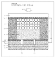
- FIG. 1 is a cross-sectional view schematically showing a configuration example of a dye-sensitized solar cell in an embodiment of the present invention.
- the dye-sensitized solar cell includes a photoelectrode on which sunlight 10 is incident, a counter electrode facing the photoelectrode, and an electrolytic solution 15 held between both electrodes.
- the photoelectrode is formed by a transparent photoelectrode layer (electrode layer, first electrode layer) 12a formed on a transparent photoelectrode substrate (first substrate) 11, and on the photoelectrode layer 12a, an increase is made.
- a semiconductor porous layer 13 carrying a dye-sensitive material is formed.
- the semiconductor porous layer 13 is made of, for example, nano-sized titanium oxide (TiO 2 ), and the sensitizing dye is, for example, a ruthenium bipyridyl complex.
- the counter electrode is formed by a counter electrode substrate (second substrate) 18a made of metal, a corrosion-resistant conductive layer 17a, and a conductive catalyst layer 16 formed thereon.
- the counter electrode substrate 18a, the corrosion-resistant conductive layer 17a, and the conductive catalyst layer 16 constitute a counter electrode layer (second electrode layer) 12b.
- the counter electrode substrate 18a serves as a support for the conductive catalyst layer 16. Used as a current collector.
- the counter electrode substrate 18a is, for example, a low-resistance metal substrate such as aluminum, copper, or stainless steel (SUS), and the corrosion-resistant conductive layer 17a is, for example, chromium, nickel, titanium, ruthenium, or the like.
- the electrolyte solution 15 is, for example, a solution in which a redox system of iodine and iodine ions is dissolved in a nitrile solvent.
- the electrolyte solution 15 filled from the electrolyte solution injection holes 20a and 20b is sealed between the photoelectrode and the counter electrode by the main seal (sealant 14a), end seal (sealant 14b), and end seal plate 19. Is retained.
- the electrons in the ground state of the sensitizing dye are excited and transition to the excited state, and the excited electrons are injected into the conduction band of the titanium oxide semiconductor and collected in the electrode layer 12a.
- the electrons that have moved to the counter electrode are carried by the ions in the electrolyte solution 15 and return to the ground state sensitizing dye.
- the reductant I ⁇ is oxidized on the photoelectrode side to become an oxidant I 3 ⁇ , and the oxidant I 3 ⁇ is reduced on the counter electrode side to return to the original reductant I ⁇ . That is, the oxidation reaction of the reducing agent I ⁇ on the photoelectrode side (3I ⁇ ⁇ I 3 ⁇ + 2e ⁇ ), and the reduction reaction of the oxidizing agent I 3 ⁇ (a conjugate of I 2 and I ⁇ ) on the counter electrode (I 3 ⁇ + 2e ⁇ ⁇ 3I ⁇ ), light is converted into current and electric energy is extracted to the outside.
- Photoelectrode substrate (first substrate) As the photoelectrode substrate (first substrate) 11, a substrate having high transparency in the visible light region, excellent barrier properties against various gases such as water and oxygen, and organic solvents, and excellent in solvent resistance and weather resistance, A transparent inorganic substrate or a transparent resin substrate can be used.
- the transparent inorganic substrate for example, quartz, sapphire, glass and the like can be used.
- a transparent resin substrate for example, polyethylene terephthalate (PET), triacetyl cellulose (TAC), polyethylene naphthalate (PEN), polycarbonate (PC), polymethyl methacrylate (PMMA), polyester, polypropylene (PP), polyarylate (PAr) ), Polyethersulfone (PES), polyetheretherketone (PEEK), polyphenylene sulfide (PPS), polyvinylidene fluoride, polyimide (PI), polyamide (PA), polysulfone (PS), polyetherimide (PEI), Polyolefin, polystyrene, polymethylpentene, cellulose triacetate and the like can be used.
- PET polyethylene terephthalate
- TAC triacetyl cellulose
- PEN polyethylene naphthalate
- PC polycarbonate
- PMMA polymethyl methacrylate
- PET polypropy
- Photoelectrode layer (electrode layer, first electrode layer) for example, MgO (Magnesium Oxide), ZnO (Zinc Oxide), SnO 2 (Tin Oxide), FTO (Fluorine doped Tin Oxide), GTO (Gallium Tin Oxide) ), ITO (Indium Tin Oxide), ATO (Antimony doped Tin Oxide), AZO (Aluminum doped Zinc Oxide), GZO (Gallium doped Zinc Oxide), IZO (Indium Zinc Oxide), and other transparent electrodes can be used.
- MgO Magnetic Oxide
- ZnO Zinc Oxide
- SnO 2 Tin Oxide
- FTO Fluorine doped Tin Oxide
- GTO Gaallium Tin Oxide
- ITO Indium Tin Oxide
- ATO Antimony doped Tin Oxide
- AZO Alluminum doped Zinc Oxide
- GZO Gaallium doped Zinc Oxide
- IZO Indium Zinc Oxide
- the counter electrode substrate (second substrate) 18 a is a support and a current collector for the conductive catalyst layer 16.
- the material of the counter electrode substrate 18a is any one of aluminum (Al), copper (Cu), silver (Ag), gold (Au), and stainless steel (SUS).
- SUS is an alloy containing about 12% or more of chromium in iron (Fe), and includes aluminum (Al), titanium (Ti), manganese (Mn), nickel (Ni), copper (Cu), Niobium (Nb), molybdenum (Mo) or the like may be added, and typically, SUS304 and SUS403 general-purpose products can be used.
- the side surface of the counter electrode substrate 18a facing the electrolyte solution 15 is a mirror surface and a light reflecting surface.
- the corrosion-resistant conductive layer 17a includes titanium (Ti), chromium (Cr), nickel (Ni), niobium (Nb), molybdenum (Mo), ruthenium (Ru), rhodium (Rh), tantalum (Ta), tungsten ( W), iridium (Ir), platinum (Pt), or hastelloy.
- the corrosion-resistant conductive layer 17a is chromium or nickel, and the chromium layer or nickel layer is formed on the counter electrode substrate 18a, the corrosion-resistant conductive layer 17a is formed in close contact with the counter electrode substrate 18a,
- the conductive catalyst layer 16 serves as a base layer, and the conductive catalyst layer 16 can be formed in close contact with the base layer.
- the conductive catalyst layer 16 is a layer that has a catalytic activity to promote a reduction reaction for reducing the oxidized form of the redox pair contained in the electrolyte solution 15 to a reduced form, and functions as a catalyst. It has corrosion resistance against iodine in it.
- Examples of the conductive catalyst layer 16 having catalytic activity for a redox pair include, for example, carbon (C), ruthenium (Ru), rhodium (Rh), palladium (Pd), osmium (Os) having conductivity and catalytic activity. ), Iridium (Ir), platinum (Pt), a conductive polymer (conductive polymer), or the like can be used.
- a material for forming the conductive catalyst layer platinum having a high corrosion resistance against components contained in the electrolyte solution is particularly suitable.
- Examples of conductive polymers include polypyrrole, polythiophene, polyaniline, polyfuran, poloacetylene, polyphenylene, polyazulene, polyfluorene, and derivatives thereof, poly (3,4-ethylenedioxythiophene) / polystyrene sulfonic acid (PEDOT / PSS), etc. Can be used.
- the semiconductor material constituting the semiconductor porous layer 13 is preferably an n-type semiconductor material in which conduction band electrons become carriers under photoexcitation to generate an anode current, and anatase-type titanium oxide TiO 2 is preferable.
- anatase-type titanium oxide TiO 2 is preferable.
- MgO, ZnO, SnO 2, WO 3, Fe 2 O 3, In 2 O 3, Bi 2 O 3, Nb 2 O 5, SrTiO 3, BaTiO 3, ZnS, CdS, CdSe, CdTe, PbS, CuInS InP or the like can be used.
- sensitizing dye As the sensitizing dye to be supported on the semiconductor fine particles, those formed in a complex with a metal such as ruthenium (Ru), zinc (Zn), platinum (Pt), palladium (Pd) can be used.
- a metal such as ruthenium (Ru), zinc (Zn), platinum (Pt), palladium (Pd)
- a typical example is a ruthenium complex dye coordinated with a ligand such as a bipyridine structure or a terpyridine structure.
- L is 4,4′-dicarboxy-2,2′-bipyridine
- L ′ is 4,4 ′, 4 ′′ -tetra-carboxy-2,2 ′, 2 ′′ -terpyridine
- TBA is Tetrabutylammonium cation.
- Ru bipyridine complex compounds are particularly preferred because of their high quantum yield.
- dyes for example, xanthene dyes, cyanine dyes, porphyrin dyes, anthraquinone dyes, polycyclic quinone dyes, and the like can be used as long as they provide a sensitizing action.
- the electrolyte solution 15 includes an iodine (I 2) a combination electrolyte and water or various organic solvents to dissolve them consisting of (iodine / iodide) iodide (a metal iodide or an organic iodide), I 3 - / I - generating a redox couple (redox pair).
- I 2 a combination electrolyte and water or various organic solvents to dissolve them consisting of (iodine / iodide) iodide (a metal iodide or an organic iodide), I 3 - / I - generating a redox couple (redox pair).
- the metal iodide is, for example, LiI, NaI, KI, CsI, CaI 2 , and the like
- the organic iodide is, for example, tetraethylammonium iodide, tetrapropylammonium iodide, tetrabutylammonium iodide, and the like.
- the electrolyte solution 15, bromine (Br 2) and comprises an electrolyte and water or various organic solvents to dissolve them consisting of a combination of metal bromide or an organic bromide, Br 3 - generating a redox couple (redox pair) - / Br It can also be set as the structure to do.
- the compound corresponding to said metal iodide or organic iodide can be used as a metal bromide or an organic bromide.
- water, various organic solvents, or ionic liquids can be used as the solvent of the electrolyte solution 15.
- the organic solvent include alcohols such as methanol, ethanol, isopropyl alcohol, ethylene glycol, propylene glycol, and polyethylene glycol, ethers such as dioxane and diethyl ether, nitriles such as acetonitrile and benzonitrile, ethylene carbonate, propylene carbonate, and the like.
- Organic solvents such as gamma-butyrolactone, pyridine, dimethylformamide, dimethylacetamide, and dimethyl sulfoxide can be used in addition to the carbonate-based solvents.
- ionic liquid methylpropylimidazolium-iodine (MPII) or the like can be used as the ionic liquid.
- the electrolyte solution may contain an additive composed of an inorganic compound or an organic compound.
- the main seal 14a keeps a gap between the photoelectrode and the counter electrode and prevents intrusion of moisture, oxygen, carbon dioxide, etc. from the outside, and the end seal 14b closes the electrolyte solution injection holes 20a, 20b.
- the end seal plate 19 In combination with the end seal plate 19, entry of moisture, oxygen, carbon dioxide and the like from the outside and leakage of the electrolyte solution 15 to the outside are suppressed.
- the main seal 14a and the end seal 14b for example, an epoxy resin, an acrylic resin, or the like can be used.
- a resin that can be cured by heat or ultraviolet rays and has a gas barrier property can be used.
- the main seal 14a and the end seal 14b may be the same type of resin or different types of resin.
- the main seal 14a and the end seal 14b in order to suppress deterioration of the electrolyte solution 15 and the sensitizing dye due to high temperature exposure at the time of curing of the resin, the main seal 14a and the end seal 14b are not modified even when contacting with the electrolyte solution 15 before and after curing. It is preferable to use an ultraviolet curable resin that does not decrease in strength and has good iodine resistance and can be cured at a low temperature. Moreover, it is more desirable that the permeability of the electrolyte solution 15 to the solvent, water, and oxygen after curing is small.
- the outline of the production process of the dye-sensitized solar cell is as follows. First, the main seal 14a is applied on the photoelectrode layer 12a so as to surround the semiconductor porous layer 13 carrying the sensitizing dye in an annular shape, and the photoelectrode layer and the counter electrode are bonded so as to maintain a desired gap. To do. Next, the electrolyte solution 15 is injected (filled) into one of the gaps from one of the electrolyte solution injection holes 20a and 20b formed in the counter electrode substrate 18a. Finally, the end seal plate 19 is joined to the counter electrode substrate 18a by the end seal 14b, and the electrolyte solution 15 is blocked from the outside and sealed to prevent leakage to the outside.
- the main seal 14a and the end seal 14b are made of materials that are difficult to permeate various gases and liquids and are resistant to corrosion deterioration.
- the end seal plate 19 is a glass plate, metal plate, or the like having similar properties. Is used. Further, the electrolyte solution 15 may be injected from an injection hole provided in addition to the second electrode layer 12b.
- the counter electrode substrate 18a is inexpensive, such as aluminum, copper, stainless steel, etc., and even when a low resistance metal substrate is used, it has corrosion resistance against iodine and has a low resistance.
- a corrosion-resistant conductive layer on the surface of the counter electrode substrate 18a with metal, corrosion due to the electrolyte solution can be suppressed, and the series resistance is reduced and the fill factor (FF factor) is increased.
- FF factor fill factor
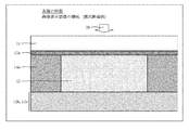
- FIG. 2 is a cross-sectional view schematically showing a configuration example of the dye-sensitized solar cell in the embodiment of the present invention.
- the counter electrode substrate (second substrate) 18b is a metal plate having corrosion resistance against iodine.
- the counter electrode substrate 18b, the corrosion-resistant conductive layer 17b, and the conductive catalyst layer 16 constitute a counter electrode layer (second electrode layer) 12c, and the counter electrode substrate 18b serves as a support for the conductive catalyst layer 16. Used as a current collector.
- the counter electrode substrate 18b is made of titanium (Ti), niobium (Nb), molybdenum (Mo), ruthenium (Ru), rhodium (Th), tantalum (Ta), tungsten (W), iridium (Ir), platinum (Pt).
- the corrosion-resistant conductive layer 17b is made of chromium (Cr) or nickel (Ni).
- the chromium layer or the nickel layer as the corrosion-resistant conductive layer 17b is formed in close contact with the counter electrode substrate 18b, and serves as a base layer for the conductive catalyst layer 16, and is in close contact with the base layer to be conductive.
- the catalyst layer 16 can be formed.
- Hastelloy is an alloy containing nickel (Ni) as a main component, such as Hastelloy B, Hastelloy CX, Hastelloy G, chromium (Cr), iron (Fe), cobalt (Co), copper (Cu), molybdenum (Mo), What contains tungsten (W) etc. in a different component amount can be used.
- the counter electrode substrate 18b can be made of chromium or nickel.
- the counter electrode substrate 18b can also serve as the corrosion-resistant conductive layer 17b, and the corrosion-resistant conductive layer 17b is specially formed. There is no need to form.
- the side surface of the counter electrode substrate 18b facing the electrolyte solution 15 is a mirror surface and a light reflecting surface.
- the counter electrode substrates 18a and 18b serve as a support for the conductive catalyst layer 16 and are used as a current collector. Is done.
- the thickness is set to 0.4 mm to 2 mm, preferably 0.5 mm.
- FIG. 3 is a cross-sectional view schematically showing an arrangement example of the extraction electrodes of the dye-sensitized solar cell in the embodiment of the present invention.
- the semiconductor porous layer 13, the electrolyte solution 15, and the main seal 14 a existing in the range indicated by the dotted lines are omitted, and the end seal 14 b, the end seal plate 19, and the electrolyte solution injection holes 20 a and 20 b are also omitted. Only the main part is shown.
- the photoelectrode and the counter electrode are arranged in a tab structure at both ends, and an extraction electrode 21a is arranged on the surface exposed to the outside of the photoelectrode layer 12a.
- An example in which the extraction electrode 21b is arranged on the surface facing the side in contact with the electrolyte solution is shown.
- the area of the counter electrode substrate is smaller than the area of the photoelectrode substrate, the photoelectrode and the counter electrode are arranged in a tab structure on one end side, and the photoelectrode layer 12a
- An example is shown in which the extraction electrode 21a is disposed on the surface exposed to the outside, and the extraction electrode 21b is disposed on the surface of the counter electrode substrate 21b facing the side in contact with the electrolyte solution.
- the series resistance of the dye-sensitized solar cell can be reduced.
- the arrangement of the extraction electrode shown in FIG. the size of the dye-sensitized solar cell can be reduced, and the number of dye-sensitized solar cells that can be arranged per unit area can be increased.
- FIG. 4 is a cross-sectional view schematically showing a manufacturing process of the counter electrode layer of the dye-sensitized solar cell in the embodiment of the present invention.
- FIG. 4A shows a manufacturing process of the counter electrode layers 12b and 12c used in the dye-sensitized solar cell of the configuration example (part 1) shown in FIG.
- openings that penetrate through the counter electrode substrates 18a and 18b are formed.
- corrosion-resistant conductive layers 17a and 17b are formed on one surface of the counter electrode substrates 18a and 18b and the inner surface of the opening.
- the conductive catalyst layer 16 is formed on the surfaces of the corrosion-resistant conductive layers 17a and 17b including the inner surface of the opening.
- the manufacturing process shown in FIG. 4A is applied when a metal substrate with poor iodine resistance is used. Needless to say, it can also be applied when using a metal substrate with good iodine resistance. In this case, the corrosion-resistant conductive layers 17a and 17b can be omitted.
- FIG. 4B shows a manufacturing process of the counter electrode layer 12c used in the dye-sensitized solar cell of the configuration example (part 2) shown in FIG.
- a corrosion-resistant conductive layer 17b is formed on one surface of the counter electrode substrate 18b.
- the conductive catalyst layer 16 is formed on the surface of the corrosion-resistant conductive layer 17b.
- an opening that penetrates the conductive catalyst layer 16, the corrosion-resistant conductive layer 17b, and the counter electrode substrate 18b is formed.
- the manufacturing process shown in FIG. 4B is applied when a metal substrate having good iodine resistance is used.
- the corrosion-resistant conductive layer 17b is Can be omitted.
- the metal ion that is deposited on the electrode and develops color by reduction is, for example, metal ions such as silver, bismuth, copper, iron, chromium, nickel.
- the electrolyte solution is a solution in which these metal iodides and iodates are dissolved. When the bismuth compound and the silver compound are dissolved, the electrolyte solution is almost transparent, a dark precipitate is generated on the electrode, and the decoloring reversible reaction is good.
- FIG. 5 is a cross-sectional view schematically showing a configuration example of an image display device (electrochromic device) in the embodiment of the present invention.
- the conductive catalyst layer 16 the corrosion-resistant conductive layers 17a and 17b, the counter electrode substrates (second substrates) 18a and 18b, the main seal (sealing agent) 14a, and the end seal, which are common to FIG. 1 or FIG.
- the (sealant) 14b, the end seal plate 19, and the electrolyte solution injection holes 20a and 20b are not shown and will not be described below.
- the electrochromic device includes a photoelectrode (viewing electrode) composed of a transparent photoelectrode substrate 11 and a transparent photoelectrode layer 12a formed thereon, and counter electrode layers 12b and 12c.
- An electrolyte solution 15 injected between them and a main seal 14a for sealing the electrolyte solution 15 are roughly configured.
- the electrolyte solution 15 containing metal ions deposited on the photoelectrode typically, silver iodide (AgI), silver compounds such as silver iodate (AgIO 3 ), bismuth iodide (BiI 3 ), iodine Bismuth compounds such as bismuth acid (BI (IO 3 ) 3 ) are used.
- the electrolyte solution 15 may use lithium iodide, sodium iodide, potassium iodide or the like as a supporting electrolyte.
- a display medium formed by holding the electrolyte solution 15 in a white material and formed into a sheet may be disposed between the photoelectrode and the counter electrode so that white display is performed when black display is not performed.
- This display medium can be formed by using a resin that is soluble in the solvent of the electrolyte solution 15 and holding the electrolyte solution 15 in a gel state, and the resin is coated with a white pigment (titanium oxide, zinc oxide, sulfuric acid). Barium, zirconium oxide, lead oxide, etc.) can also be used dispersed.
- the side surface of the counter electrode substrate 18a, 18b facing the electrolyte solution 15 be a mirror surface and a light reflecting surface in order to brighten the display screen (viewing surface).
- the electrode layer 12a is formed as a fraction, that is, a plurality of fractions which are mutually independent so as to correspond to each pixel are formed in a matrix, and a gate line and a source corresponding to each fraction are formed.
- Transparent thin film transistors hereinafter referred to as transparent TFTs
- active matrix driving can be performed to control the color generation / decoloration in the fraction corresponding to each pixel.
- the electrochromic device described here is a display device using an electrochromic dye that reversibly develops or loses color by an oxidation-reduction reaction by application of a voltage.
- FIG. 6 is a cross-sectional view schematically showing a configuration example of an image display device (electrochromic device) in the embodiment of the present invention.
- the conductive catalyst layer 16 the corrosion-resistant conductive layers 17a and 17b, the counter electrode substrates (second substrates) 18a and 18b, the main seal (sealing agent) 14a, and the end seal, which are common to FIG. 1 or FIG. (Sealant) 14b, end seal plate 19, electrolyte solution 15, and electrolyte solution injection holes 20a and 20b are not shown and will not be described below.
- the electrochromic device includes a photoelectrode (viewing electrode) comprising a transparent photoelectrode substrate 11 and a transparent photoelectrode layer 12a formed thereon, and a counter electrode layer 12b. , 12c, an electrolyte solution 15, and a main seal 14a for sealing the electrolyte solution 15, and a semiconductor porous layer 23 carrying an electrochromic dye.
- a photoelectrode viewing electrode
- 12c an electrolyte solution
- main seal 14a for sealing the electrolyte solution
- the side surfaces of the counter electrode substrates (second substrates) 18a and 18b facing the electrolyte solution 15 be mirror surfaces and light reflection surfaces from the viewpoint of brightening the display screen (viewing surface).
- the components of the electrochromic device will be described sequentially.
- the conductive catalyst layer 16, the corrosion-resistant conductive layers 17a and 17b, the counter electrode substrates 18a and 18b, the main seal (sealing agent) 14a, and the end seal (sealing) that are common to FIG. 1 or FIG. Agent) 14b, end seal plate 19, electrolyte solution 15, and electrolyte solution injection holes 20a and 20b will not be described.
- the semiconductor porous layer 23 on which the electrochromic dye is supported is made of a material having a large surface area in order to obtain a high support function of the electrochromic dye.
- the semiconductor porous layer 23 can be formed of, for example, an oxide semiconductor, a complex oxide semiconductor, or the like.
- oxide semiconductor include TiO 2 , SnO 2 , Fe 2 O 3 , SrTiO 3 , WO 3 , ZnO, ZrO 2 , Ta 2 O 5 , Nb 2 O 5 , V 2 O 5 , In 2 O 3 , CdO, MnO, CoO, TiSrO 3 , KTiO 3 , Cu 2 O, sodium titanate, barium titanate, potassium niobate and the like can be used.
- Examples of the complex oxide semiconductor include SnO 2 —ZnO, Nb 2 O 5 —SrTiO 3 , Nb 2 O 5 —Ta 2 O 5 , Nb 2 O 5 —ZrO 2 , Nb 2 O 5 —TiO 2 , Ti —SnO 2 , Zr—SnO 2 , Sb—SnO 2 , Bi—SnO 2 , In—SnO 2 and the like can be used, and TiO 2 , SnO 2 , Sb—SnO 2 , and In—SnO 2 are particularly preferable. Can be used for.
- any known material can be used for the electrochromic dye supported on the surface of the semiconductor porous layer 23 and the internal micropores.
- organic compound or an inorganic compound can be used as the electrochromic dye.
- organic compounds that can be used include organic dyes such as viologen dyes, styryl dyes, fluorane dyes, cyanine dyes and aromatic amine dyes, and organometallic complexes such as metal-bipyridyl complexes and metal-phthalocyanine complexes.
- the metal is a rare earth metal, lutetium (Lu), ytterbium (Yt), gadolinium (Gd), neodymium (Nd), europium (Eu), lanthanum (La), cerium (Ce), erbium (Er), yttrium ( Y)).
- the photoelectrode layer 12a is fractionated so as to correspond to the pixels, that is, the matrix-like photoelectrode layer 12a composed of a plurality of fractions is formed on the photoelectrode substrate.
- the semiconductor porous layer 23 is formed on each fraction.
- An electrochromic dye is supported on the semiconductor porous layer 23 formed on each fraction.
- the electrochromic dye is any compound capable of coloring magenta (M), yellow (Y), and cyan (C).
- a transparent TFT connected by a gate line and a source line is formed and arranged corresponding to each fraction. According to this apparatus, by controlling the voltage applied to the transparent TFT, it is possible to control the color generation / deactivation in the fraction corresponding to each pixel, and magenta (M), yellow (Y), cyan ( Image display based on any one of the color generation and extinction of C) becomes possible.
- the electrochromic device shown in FIG. 6A can be configured to enable full color display.
- the photoelectrode layer 12a is fractionated and formed to correspond to the pixels, that is, the first corresponding to magenta (M), yellow (Y), and cyan (C).
- a matrix-like photoelectrode layer 12a comprising a plurality of fractions comprising the second and third fractions is formed on the photoelectrode substrate 11.
- a semiconductor porous layer 23 is formed on the first, second, and third fractions, and magenta (M) is formed on the semiconductor porous layer 23 formed on the first, second, and third fractions, respectively.
- a transparent TFT connected by a gate line and a source line is formed and disposed on the transparent electrode 2 corresponding to the first, second, and third fractions.
- the electrochromic device configured as described above, by controlling the voltage applied to the transparent TFT, the color generation / decoloration in the first, second and third fractions corresponding to each pixel is controlled, Full color display can be made possible.
- an electrochromic device that enables full color display by laminating three layers of electrochromic devices having basically the same structure as that shown in FIG.
- FIG. 6B is a cross-sectional view illustrating a schematic configuration of an example of an electrochromic device capable of performing color display according to an embodiment of the present invention.
- Each of the electrochromic element structures 10A, 10B, and 10C shown in FIG. 6B has basically the same configuration as that shown in FIG. 6B.
- the semiconductor porous layer 23a of the display structure 40A, the semiconductor porous layer 23b of the display structure 40B, and the semiconductor porous layer 23c of the display structure 40C shown in FIG. 6B are respectively magenta (M) and yellow.
- An electrochromic dye that develops color (Y) and cyan (C) is supported.
- the electrolyte solutions 15 in the display structures 40A, 40B, and 40C may be the same or different.
- the transparent photoelectrode layer 12a is fractionated so as to correspond to the pixels, that is, the matrix-like photoelectrode layer 12a composed of a plurality of fractions is a transparent photoelectrode.
- a semiconductor porous layer 23a, 23b, 23c is formed on the substrate 11 and on each fraction.
- electrochromic dyes that develop colors of magenta (M), yellow (Y), and cyan (C) are supported.
- the counter substrates 18a and 18b in the display structure 40C are metal plates as shown in FIG. 1 or 2, and the counter electrode layers 12b and 12c are opaque, but the counter substrates 18a and 18b in the display structures 40A and 40B are opaque.
- 18b is formed of a transparent material, and the counter electrode layer (second electrode layer) 12d is substantially transparent.
- a full color display electrochromic device capable of reversibly performing color generation and decoloration can be configured.
- transparent TFTs connected by gate lines and source lines are formed corresponding to the respective fractions of the photoelectrode layer 12a for the display structures 40A, 40B, and 40C.
- Each of the display structures 40A, 40B, and 40C is driven by active matrix driving by controlling the voltage applied to the transparent TFT formed in each fraction of the photoelectrode layer 12a for each of the display structures 40A, 40B, and 40C. It is possible to control the color generation / decoloration in the fraction corresponding to each pixel in the image, and display an image based on the color generation / deactivation of magenta (M), yellow (Y), and cyan (C).
- M magenta
- Y yellow
- C cyan
- the electrochromic dyes include yellow (Y) region (430 to 490 nm range), magenta (M) region (500 to 580 nm range), cyan (C) region (600 to 700 nm). It is desirable to use a dye having an absorption maximum in the range (1).
- an electrochromic dye capable of developing cyan (C) for example, 2- ⁇ 2- [4- (methoxy) phenyl] -1,3,5-hexatrienyl ⁇ -3,3-dimethyl-5-phospho Noindolino [2,1-b] (2- [2- [4- (methoxy) phenyl] -1,3,5-hexatrienyl-3,3-dimethyl-5-phosphonoindolino [2,1-b] oxazolidine ]) Can be used.
- an electrochromic dye capable of developing magenta for example, 2- ⁇ 2- [4- (dimethylamino) phenyl] -1,3-butadienyl ⁇ -3,3-dimethyl-5-carboxylindo Reno [2,1-b] oxazoline (2- [2- [4- (dimethylamino) phenyl] -1,3-butadienyl] -3,3-dimethyl-5-carboxylindolino [2,1-b] oxazolidine) Can be used.
- M magenta
- an electrochromic dye capable of developing yellow (Y) for example, 2- ⁇ 2- [4- (dimethylamino) phenyl] ethenyl ⁇ -3,3-dimethyl-5-phosphonoindolino [2, 1-b] oxazoline (2- [2- [4- (dimethylamino) phenyl] ethenyl] -3,3-dimethyl-5-phosphonoindolino [2,1-b] oxazolidine) can be used.
- An anti-glare mirror using an electrochromic coloring layer is a mirror that can adjust the reflectance and suppress glare by utilizing the degree of color change of the electrochromic coloring layer depending on the applied voltage. .
- FIG. 7 is a cross-sectional view schematically showing a configuration example of the anti-glare mirror in the embodiment of the present invention.
- the anti-glare mirror includes a transparent photoelectric substrate 11 on the viewing side, a transparent photoelectrode layer 12a formed thereon, and a coloring layer 33 containing an electrochromic compound formed thereon.
- the electrolyte solution 15 is sealed and roughly configured in a gap between the color-developing electrode made of the electrode and the counter electrode layers (counter electrodes) 12b and 12c similar to those shown in FIG. 1 or FIG.
- the counter electrode substrates (second substrates) 18a and 18b of the counter electrode layers 12b and 12c preferably have smoothness because their surfaces become light reflecting layers.
- the counter electrode substrates 18a and 18b have a configuration in which a metal layer having corrosion resistance to iodine is formed on the surface of a metal plate such as aluminum, SUS, or copper.
- the conductive catalyst layer 16 In FIG. 7, the conductive catalyst layer 16, the corrosion-resistant conductive layers 17a and 17b, the counter electrode substrates 18a and 18b, the main seal (sealing agent) 14a, and the end seal (sealing agent) 14b, which are common to FIG. 1 or FIG.
- the end seal plate 19, the electrolyte solution 15, and the electrolyte solution injection holes 20 a and 20 b are not illustrated and will not be described below.
- the coloring layer 33 is made of, for example, tungsten oxide (WO 3 ), vanadium oxide (V 2 O 5 ), molybdenum oxide (Mo 2 O 3 ), iridium oxide (Ir 2 O 3 ), nickel oxide (NiO), manganese oxide ( It is preferable to be formed of a reduced coloring type oxide such as MnO 2 ), and the coloring layer 33 can be formed on the photoelectrode layer 12a by a known method.
- the intensity of the reflected light from the counter electrode becomes substantially constant, Since the reflectance can be adjusted by changing the degree of coloring of the coloring layer 33, the degree of glare in the viewing direction 30 can be made substantially constant.
- Example > The dye-sensitized solar cell in the example of the present invention has the configuration shown in FIG.
- a glass substrate (15 mm ⁇ 20 mm square, sheet resistance 10 ⁇ / ⁇ , manufactured by Nippon Sheet Glass Co., Ltd.) (photoelectrode substrate 11) on which a fluorine-doped tin oxide conductive layer (FTO layer) is formed as a photoelectrode layer 12a is a photoelectrode It was.
- FTO layer fluorine-doped tin oxide conductive layer
- a semiconductor porous layer 13 was formed on the FTO layer.
- FIG. 8 is a diagram showing an example of the sensitizing dye used in the dye-sensitized solar cell in the example of the present invention.
- FIG. 8A shows trithiocyanato (4,4 ′, 4 ′′ -tricarboxy-2,2 ′: 6 ′, 2 ′′ -terpyridine) ruthenium (II) tri-tetrabutylammonium complex (Solaronix, 620 -1H3TBA, Batch Number 34) (black dye, commonly referred to as N749).
- TBA in FIG. 8A is tetrabutammonium (N ((CH 2 ) 3 CH 3 ) 4 ).
- B) of FIG. 8 is merocyanine pigment
- TiO 2 titanium oxide (TiO 2 ) semiconductor porous layer was added to a mixed dye liquid composed of D131 (concentration 0.1875 mM) and black die (concentration 0.5625 mM). The pigment was supported on titanium oxide (TiO 2 ) by soaking for 96 hours.
- a 0.4 mm-thick Nb, Ru, Ti plate is used as the counter electrode substrate 18b, and a 500-thick Cr layer is formed as the corrosion-resistant conductive layer 17b, and a 1000-thick Pt as the conductive catalyst layer 16 is formed on this Cr layer.
- a layer was formed as a counter electrode.
- the Cr layer and the Pt layer were formed by sputtering. In the following description including FIG. 10 and FIG. 11, these counter electrodes are abbreviated as Nb / Cr / Pt, Ru / Cr / Pt, and Ti / Cr / Pt.
- FIG. 9 is a diagram showing a composition example of the electrolyte solution used in the dye-sensitized solar cell in the example of the present invention.
- acetonitrile was used as a solvent, and sodium iodide (concentration 0.15M), DMPImI (concentration 0.9M), iodine (concentration 0.05M), t-butylpyridine (concentration 0.1M).
- DMPImI 1,2-dimethyl-3-propyl-1H-imidazole-3-iumiodide (C 8 H 15 N 2 ).
- One of the electrolyte solution injection holes 20a and 20b formed in the counter electrode was used as an air vent hole, and the electrolyte solution 15 was injected from the other hole into the internal space formed by the joined photoelectrode and counter electrode.
- the electrolyte solution injection holes 20a and 20b were sealed using a glass plate as the end seal plate 19 and an ultraviolet curable resin (31X-101 series resin, manufactured by ThreeBond Co., Ltd.) as the end seal 14b, respectively.
- the gap distance between the bonded photoelectrode and the counter electrode is 30 ⁇ m, and the light irradiation area of the internal space is 150 mm ⁇ 150 mm.
- Comparative example > A 0.4 mm-thick alumina (Al 2 O 3 ) plate (insulator substrate) is used as the counter electrode substrate 18b, a 500-thick Cr layer is formed as the corrosion-resistant conductive layer 17b, and the conductive catalyst layer 16 is formed on this Cr layer.
- a counter electrode a Pt layer having a thickness of 1000 mm was formed. The Cr layer and the Pt layer were formed by sputtering.
- this counter electrode is abbreviated as alumina / Cr / Pt. Since other configurations are the same as those of the embodiment, description thereof is omitted.
- FIG. 10 is a diagram showing an example of photoelectric conversion characteristics of the dye-sensitized solar cell in the example of the present invention.
- FIG. 10 shows the result regarding the dye-sensitized battery having the counter electrode alumina / Cr / Pt in the comparative example, and (b), (c), and (d) respectively show the counter electrode Nb / in the example.
- the result regarding the dye-sensitized battery which has Cr / Pt, Ru / Cr / Pt, Ti / Cr / Pt is shown.
- FIG. 10 shows the current-voltage characteristics of the dye-sensitized solar cell, where the horizontal axis represents voltage (V) and the vertical axis represents current density J (mA / cm 2 ).
- V voltage
- J current density
- the fill factor FF of the dye-sensitized solar cell of the comparative example is 1.0
- the fill factor FF of the dye-sensitized solar cells (b), (c), and (d) of the examples is 1.13, respectively. 1.08, 1.10.
- the dye-sensitized solar cell of Example (b), (c), the photoelectric conversion efficiency E ff of (d) are 1.12, 1.04, and 1.09, respectively.
- FIG. 11 shows an example of a Cole-Cole plot diagram showing the impedance characteristics of the dye-sensitized solar cell in the example of the present invention.
- the horizontal axis represents the real part Z ′ ( ⁇ ) of the impedance
- the vertical axis represents the imaginary part Z ′′ ( ⁇ ) of the impedance.
- FIG. 11 is a schematic sectional view showing the layer structure of the counter electrode.
- FIG. 11 shows the result regarding the dye-sensitized battery having the counter electrode alumina / Cr / Pt in the comparative example.
- FIG. 11 shows the results (two curves indicated by small solid circles) regarding two samples of the dye-sensitized battery having the counter electrode Nb / Cr / Pt in the example. The reproducibility of the impedance characteristics for the two samples is good.
- the impedance characteristics of the dye-sensitized solar cell shown in FIG. 11 are such that the lower the resistance between the counter electrode and the electrolyte solution, the lower the real part Z ′ is at the starting position of the arc, so the counter electrode Nb / Cr / Pt
- the series resistance of a dye-sensitized solar cell using a lower electrode is lower than the series resistance of a counter-electrode using an alumina substrate (insulator substrate), that is, a dye-sensitized solar cell using a counter electrode alumina / Cr / Pt. It shows that.
- the sheet resistance of the counter electrode in the above-described example is 8.8 ⁇ 10 ⁇ 4 ⁇ / cm 2 for Nb / Cr / Pt, 8.4 ⁇ 10 ⁇ 4 ⁇ / cm 2 for Ru / Cr / Pt, The Ti / Cr / Pt was 9.0 ⁇ 10 ⁇ 4 ⁇ / cm 2 .
- the sheet resistance of the counter electrode (glass / Cr / Pt) in which alumina was replaced with glass in the counter electrode of the comparative example was 2.0 ⁇ / cm 2 .
- the sheet resistance of the counter electrode of the comparative example is expected to be three orders of magnitude greater than the sheet resistance of the counter electrode of the example.
- the structure using the counter electrode using the metal substrate in particular, the structure using the counter electrode Nb / Cr / Pt in which the Cr layer and Pt are formed on the Nb substrate, and the electrolyte containing iodine. Corrosion resistance to the solution is improved, and the sheet resistance of the counter electrode can be reduced and the series resistance of the dye-sensitized solar cell can be lowered than the configuration using the counter electrode using the insulating substrate. And photoelectric conversion characteristics could be improved.
- a photoelectrode substrate, a photoelectrode layer, a conductive catalyst layer, a corrosion-resistant conductive layer, a counter electrode substrate, a counter electrode layer, a semiconductor porous layer carrying a sensitizing dye or an electromic dye For example, in a functional device, a photoelectrode substrate, a photoelectrode layer, a conductive catalyst layer, a corrosion-resistant conductive layer, a counter electrode substrate, a counter electrode layer, a semiconductor porous layer carrying a sensitizing dye or an electromic dye,
- the composition of the color-forming layer containing the compound, the sealing agent, the electrolyte solution, and the like are not limited to those exemplified in the embodiments and examples, and can be appropriately changed according to the intended use.
- the present invention can also be applied to functional devices such as chemical batteries, biosensors, and capacitors as long as the electrolyte solution is used.
- the present invention can provide a functional device that uses a metal substrate to suppress corrosion due to an electrolyte solution and can reduce direct current resistance.
Abstract
Description
[色素増感太陽電池の構成例(その1)]
図1は、本発明の実施の形態における、色素増感太陽電池の構成例を模式的に示す断面図である。
光電極基板(第1の基板)11として、可視光領域の透過性が高く、水、酸素等の各種のガス及び有機溶媒の遮断性に優れ、耐溶剤性及び耐候性に優れる基板が好ましく、透明無機基板、透明樹脂基板を使用することができる。
光電極層(電極層、第1の電極層)12aとして、例えば、MgO(Magnesium Oxide)、ZnO(Zinc Oxide)、SnO2(Tin Oxide)、FTO(Fluorine doped Tin Oxide)、GTO(Gallium Tin Oxide)、ITO(Indium Tin Oxide)、ATO(Antimony doped Tin Oxide)、AZO(Aluminum doped Zinc Oxide)、GZO(Gallium doped Zinc Oxide)、IZO(Indium Zinc Oxide)等の透明電極を使用することができる。
図1に示す構成では、対向電極基板(第2の基板)18aは、導電性触媒層16の支持体であり集電体である。対向電極基板18aの材質は、アルミニウム(Al)、銅(Cu)、銀(Ag)、金(Au)、ステンレス鋼(SUS)の何れかである。SUSは、鉄(Fe)に約12%以上のクロムを含有させた合金であり、これに、アルミニウム(Al)、チタン(Ti)、マンガン(Mn)、ニッケル(Ni)、銅(Cu)、ニオブ(Nb)、モリブデン(Mo)等が添加されたものであってもよく、代表的には、SUS304、SUS403の汎用品を使用することができる。
耐腐食性導電層17aは、チタン(Ti)、クロム(Cr)、ニッケル(Ni)、ニオブ(Nb)、モリブデン(Mo)、ルテニウム(Ru)、ロジウム(Rh)、タンタル(Ta)、タングステン(W)、イリジウム(Ir)、白金(Pt)、ハステロイの何れかによって形成されている。
導電性触媒層16は、電解質溶液15中に含有されている酸化還元対の酸化体を還元体に還元する還元反応を促進する触媒活性を有し、触媒として機能する層であり、電解質溶液15中のヨウ素に対して耐腐食性を有している。
半導体多孔質層13を構成する半導体材料は、光励起下で伝導帯電子がキャリアとなり、アノード電流を生じるn型半導体材料であることが好ましく、アナターゼ型の酸化チタンTiO2が好ましいが、この他に、例えば、MgO、ZnO、SnO2、WO3、Fe2O3、In2O3、Bi2O3、Nb2O5、SrTiO3、BaTiO3、ZnS、CdS、CdSe、CdTe、PbS、CuInS、InP等を使用することができる。
半導体微粒子に担持させる増感色素としては、ルテニウム(Ru)、亜鉛(Zn)、白金(Pt)、パラジウム(Pd)等の金属と錯体を形成したもの使用することができる。
電解質溶液15は、ヨウ素(I2)とヨウ化物(金属ヨウ化物又は有機ヨウ化物)の組合せ(ヨウ素/ヨウ化物)からなる電解質とこれを溶解する水又は各種の有機溶媒を含み、I3 - /I- 酸化還元対(レドックス対)を生成する。
メインシール14aは、光電極と対向電極の間のギャップを保持すると共に、外部からの水分、酸素、二酸化炭素等の侵入を防止し、エンドシール14bは、電解質溶液用注入孔20a、20bを閉鎖し、エンドシール板19と合わせて、外部からの水分、酸素、二酸化炭素等の侵入、及び、電解質溶液15の外部への漏洩を抑制する。
色素増感太陽電池の製造工程の概要は、次の通りである。先ず、増感色素が担持された半導体多孔質層13を環状に包囲するようにメインシール14aを光電極層12a上に塗布し、光電極層と対向電極を所望の間隙を保持するように接合する。次に、この間隙に、対向電極基板18aに形成されている電解質溶液注入用孔20a、20bの一方から電解質溶液15を注入(充填)する。最後に、エンドシール板19をエンドシール14bによって、対向電極基板18aに接合し、電解質溶液15を外部から遮断して内部に封止し、外部に漏洩しないようにする。
構成例(その2)の色素増感太陽電池の構成は、構成例(その1)とは対向電極の構成のみが相違し、他の構成は同一であるので、以下では相違する対向電極の構成のみについて説明する。
図2に示す構成では、対向電極基板(第2の基板)18bは、ヨウ素に対して耐腐食性を有する金属板である。対向電極基板18b、耐食導電層17b、導電性触媒層16の三者は対向電極層(第2の電極層)12cを構成し、対向電極基板18bは導電性触媒層16の支持体となると共に、集電体として使用される。
上述したように、構成例(その1)及び(その2)の色素増感太陽電池の構成では、対向電極基板18a、18bは導電性触媒層16の支持体となると共に、集電体として使用される。対向電極基板18a、18bを支持体及び集電体とするために、その厚さを0.4mm~2mm、好ましくは、0.5mmとする。
上述した構成例(その1)及び(その2)の色素増感太陽電池に使用される対向電極層の製作工程の概要を説明する。
ここで説明するエレクトロクロミック装置は、視認(観察)側の電極への還元電圧の印加により、電解質溶液中の金属イオンが金属に還元され、電極に析出し黒色に発色し、視認側の電極を極性反転した酸化電圧の印加により、電極上に析出している金属を金属イオンに酸化して電解質溶液に溶解させ黒色の発色を消色させることによって、表示の制御を行うことができるエレクトロクロミック型の表示装置である。
ここで説明するエレクトロクロミック装置は、電圧の印加によって酸化還元反応により可逆的に発色又は消色するエレクトロクロミック色素を使用した表示装置である。
エレクトロクロミック色素が担持される半導体多孔質層23は、エレクトロクロミック色素の高い担持機能を得るため、表面積が大きい材料により構成される。
図6の(A)に示すエレクトロクロミック装置において、光電極層12aが画素に対応するよう分画されて形成され、即ち、分画の複数個からなるマトリックス状の光電極層12aが光電極基板11上に形成され、各分画上に半導体多孔質層23が形成されている。
エレクトロクロミック発色層を用いた防眩ミラーは、印加電圧によってエレクトロクロミック発色層の着色変化の程度が変化することを利用して、反射率の調整を可能として眩しさを抑えることができるミラーである。
本発明の実施例における色素増感太陽電池は図2に示す構成を有している。
フッ素をドープした酸化スズ導電層(FTO層)が光電極層12aとして形成されたガラス基板(15mm×20mm角、シート抵抗10Ω/□、日本板硝子株式会社製)(光電極基板11)を光電極とした。
上記のFTO層上に半導体多孔質層13を形成した。半導体多孔質層13を、下層に中心粒径20nmφの酸化チタン(TiO2)を15μm厚、上層に中心粒径400nmφの酸化チタン(TiO2)を5μm厚にそれぞれスクリーン印刷機を使用して塗布した後、510℃、30分間焼結処理して形成した。
図8は、本発明の実施例における、色素増感太陽電池で使用された増感色素の例を示す図である。
対向電極基板18bとして0.4mm厚のNb、Ru、Ti板を使用しそれぞれに、耐食性導電層17bとして500Å厚のCr層を形成し、このCr層に導電性触媒層16として1000Å厚のPt層を形成して、対向電極とした。Cr層及びPt層はスパッタリングによって形成した。図10、図11を含む以下の説明では、これらの対向電極を、Nb/Cr/Pt、Ru/Cr/Pt、Ti/Cr/Ptと略記する。
図9は、本発明の実施例における、色素増感太陽電池で使用された電解質溶液の組成例を示す図である。
光電極に紫外線硬化型樹脂(スリーボンド社製、31X-101系樹脂)が環状に塗布され形成されたメインシール(封止剤)14aを介して、光電極と対向電極を重ね、紫外線を照射してメインシール14aを硬化させて、光電極と対向電極を接合した。
対向電極基板18bとして0.4mm厚のアルミナ(Al2O3)板(絶縁体基板)を使用し、耐食性導電層17bとして500Å厚のCr層を形成し、このCr層に導電性触媒層16として1000Å厚のPt層を形成して対向電極とした。Cr層及びPt層はスパッタリングによって形成した。図10、図11を含む以下の説明では、この対向電極を、アルミナ/Cr/Ptと略記する。その他の構成は、実施例と同一としたので、説明は省略する。
Claims (19)
- 光透過性を有する第1の基板と、
導電性及び光透過性を有し前記第1の基板上に形成された電極層と、
金属からなる第2の基板と、
前記第1の基板と前記第2の基板の間隙に充填された電解質溶液と、
この電解質溶液に対して耐腐食性を有し前記第2の基板上に形成された耐腐食性導電層と、
導電性及び触媒活性を有し前記耐腐食性導電層の面に形成された導電性触媒層と、
を有する機能性デバイス。 - 前記金属が、アルミニウム、銅、銀、金、ステンレス鋼の何れかであり、前記耐腐食性導電層が、チタン、クロム、ニッケル、ニオブ、モリブデン、ルテニウム、ロジウム、タンタル、タングステン、イリジウム、白金、ハステロイの何れかによって形成された、請求項1に記載の機能性デバイス。
- 前記導電性触媒層が、カーボン、ルテニウム、ロジウム、パラジウム、オスミウム、イリジウム、白金、導電性高分子の何れかによって形成された、請求項2に記載の機能性デバイス。
- 前記金属が、チタン、ニオブ、モリブデン、ルテニウム、ロジウム、タンタル、タングステン、イリジウム、白金、ハステロイの何れかである、請求項1に記載の機能性デバイス。
- 前記耐腐食性導電層がクロム又はニッケルによって形成された、請求項4に記載の機能性デバイス。
- 前記金属がクロム又はニッケルであり前記耐腐食性導電層を兼ねている、請求項1に記載の機能性デバイス。
- 前記導電性触媒層が、カーボン、ルテニウム、ロジウム、パラジウム、オスミウム、イリジウム、白金、導電性高分子の何れかを含む、請求項5又は請求項6に記載の機能性デバイス。
- 前記電解質溶液は、酸化還元対I3 - /I- を生成するヨウ素/ヨウ化物を含む、請求項1から請求項7の何れか1項に記載の機能性デバイス。
- 前記間隙に前記電解質溶液を充填するための開口部が前記第2の基板を貫通して形成され、前記開口部の面に下層より前記耐腐食性導電層、前記導電性触媒層が形成された、請求項1から請求項7の何れか1項に記載の機能性デバイス。
- 前記第2の基板の面積は前記第1の基板の面積よりも小さく、前記電解質溶液と接する面に対向する前記第2の基板の面に接続される引出電極を有する、請求項1に記載の機能性デバイス。
- 光電変換機能、又は、画像表示機能、又は、防眩機能を有するデバイスとして構成された、請求項1から請求項10の何れか1項に記載の機能性デバイス。
- 光電変換機能を有するデバイスとして構成された機能性デバイスであり、増感色素が担持された半導体多孔質層が前記電極層の面に形成され、光吸収によって励起された前記増感色素の電子が前記半導体多孔質層へ取り出されるとともに、前記電子を失った前記増感色素が、前記電解質溶液中の還元剤によって還元される色素増感光電変換装置として構成された、請求項11に記載の機能性デバイス。
- 画像表示機能を有するデバイスとして構成された機能性デバイスであり、前記電解質溶液は、還元反応によって前記電極層に析出し発色する金属イオンを含む、請求項11に記載の機能性デバイス。
- 画像表示機能を有するデバイスとして構成された機能性デバイスであり、酸化反応又は還元反応により発色するエレクトロクロミック色素が担持された半導体多孔質層が前記電極層に形成された、請求項11に記載の機能性デバイス。
- 防眩機能を有するデバイスとして構成された機能性デバイスであり、酸化発色型又は還元発色型のエレクトロクロミック化合物を含む発色層が前記電極層の面に形成された、請求項11に記載の機能性デバイス。
- 金属からなる基板の面に電解質溶液に対して耐腐食性を有する耐腐食性導電層を形成する第1の工程と、
導電性及び触媒活性を有する導電性触媒層を前記耐腐食性導電層の面に形成する第2の工程と、
を有する、機能性デバイスの製造方法。 - 前記金属が、アルミニウム、銅、銀、金、ステンレス鋼の何れかであり、前記導電性触媒層が、チタン、クロム、ニッケル、ニオブ、モリブデン、ルテニウム、ロジウム、タンタル、タングステン、イリジウム、白金、ハステロイの何れかによって形成される、請求項16に記載の機能性デバイスの製造方法。
- 前記導電性触媒層が、カーボン、ルテニウム、ロジウム、パラジウム、オスミウム、イリジウム、白金、導電性高分子の何れかによって形成される、請求項17に記載の機能性デバイスの製造方法。
- 前記第1の工程に先立って前記基板に前記電解質溶液を注入するための開口部を、前記基板を貫通させて形成する工程を有し、前記第1及び第2の工程によって、前記開口部の面に下層より前記耐腐食性導電層、前記導電性触媒層が形成される、請求項17に記載の機能性デバイスの製造方法。
Priority Applications (4)
| Application Number | Priority Date | Filing Date | Title |
|---|---|---|---|
| US12/735,794 US20110048525A1 (en) | 2008-11-26 | 2007-11-26 | Functional device and method for producing the same |
| EP09829115A EP2352202A4 (en) | 2008-11-26 | 2009-11-26 | FUNCTIONAL DEVICE AND METHOD FOR MANUFACTURING THE SAME |
| CN2009801064879A CN101965662A (zh) | 2008-11-26 | 2009-11-26 | 功能性器件及功能性器件制造方法 |
| BRPI0908192-5A BRPI0908192A2 (pt) | 2008-11-26 | 2009-11-26 | Dispositivo funcional, e, método para produzir um dispositivo funcional |
Applications Claiming Priority (2)
| Application Number | Priority Date | Filing Date | Title |
|---|---|---|---|
| JP2008-301174 | 2008-11-26 | ||
| JP2008301174A JP4788761B2 (ja) | 2008-11-26 | 2008-11-26 | 機能性デバイス及びその製造方法 |
Publications (1)
| Publication Number | Publication Date |
|---|---|
| WO2010061870A1 true WO2010061870A1 (ja) | 2010-06-03 |
Family
ID=42225740
Family Applications (1)
| Application Number | Title | Priority Date | Filing Date |
|---|---|---|---|
| PCT/JP2009/069907 WO2010061870A1 (ja) | 2008-11-26 | 2009-11-26 | 機能性デバイス及びその製造方法 |
Country Status (7)
| Country | Link |
|---|---|
| US (1) | US20110048525A1 (ja) |
| EP (2) | EP2458605A1 (ja) |
| JP (1) | JP4788761B2 (ja) |
| KR (1) | KR20110086783A (ja) |
| CN (1) | CN101965662A (ja) |
| BR (1) | BRPI0908192A2 (ja) |
| WO (1) | WO2010061870A1 (ja) |
Cited By (1)
| Publication number | Priority date | Publication date | Assignee | Title |
|---|---|---|---|---|
| CN108422877A (zh) * | 2018-02-10 | 2018-08-21 | 深圳森阳环保材料科技有限公司 | 一种顶棚式太阳能充电站 |
Families Citing this family (39)
| Publication number | Priority date | Publication date | Assignee | Title |
|---|---|---|---|---|
| JP5007784B2 (ja) * | 2006-01-30 | 2012-08-22 | ソニー株式会社 | 光電変換装置 |
| JP2007234580A (ja) * | 2006-02-02 | 2007-09-13 | Sony Corp | 色素増感型光電変換装置 |
| JP2007280906A (ja) * | 2006-04-12 | 2007-10-25 | Sony Corp | 機能デバイス及びその製造方法 |
| JP5023866B2 (ja) * | 2007-07-27 | 2012-09-12 | ソニー株式会社 | 色素増感光電変換素子およびその製造方法ならびに電子機器 |
| JP2009099476A (ja) * | 2007-10-19 | 2009-05-07 | Sony Corp | 色素増感光電変換素子およびその製造方法 |
| JP2009110796A (ja) * | 2007-10-30 | 2009-05-21 | Sony Corp | 色素増感光電変換素子モジュールおよびその製造方法ならびに電子機器 |
| JP2009146625A (ja) * | 2007-12-12 | 2009-07-02 | Sony Corp | 色素増感光電変換素子モジュールおよびその製造方法ならびに光電変換素子モジュールおよびその製造方法ならびに電子機器 |
| JP2010003468A (ja) * | 2008-06-19 | 2010-01-07 | Sony Corp | 色素増感太陽電池およびその製造方法 |
| JP2010009769A (ja) * | 2008-06-24 | 2010-01-14 | Sony Corp | 光電変換素子の製造方法 |
| JP2010010191A (ja) * | 2008-06-24 | 2010-01-14 | Sony Corp | 電子装置 |
| JP5273709B2 (ja) | 2008-07-02 | 2013-08-28 | シャープ株式会社 | 色素増感太陽電池、その製造方法および色素増感太陽電池モジュール |
| JP2010092762A (ja) * | 2008-10-09 | 2010-04-22 | Sony Corp | 機能性デバイス及びその製造方法 |
| TWI384310B (zh) * | 2009-04-13 | 2013-02-01 | Univ Nat Cheng Kung | 光伏致變色元件及其應用 |
| JP5428555B2 (ja) * | 2009-06-08 | 2014-02-26 | ソニー株式会社 | 色素増感光電変換素子の製造方法 |
| KR20110083011A (ko) * | 2010-01-13 | 2011-07-20 | 삼성코닝정밀소재 주식회사 | 염료감응형 태양전지용 전극기판과 이를 구비하는 염료감응형 태양전지 |
| JP2011204662A (ja) * | 2010-03-05 | 2011-10-13 | Sony Corp | 光電変換素子およびその製造方法ならびに電子機器 |
| JP5621488B2 (ja) * | 2010-03-17 | 2014-11-12 | ソニー株式会社 | 光電変換装置 |
| JP5894372B2 (ja) * | 2010-11-01 | 2016-03-30 | パナソニック株式会社 | 光電気素子、及び光電気素子の製造方法 |
| JP2012113839A (ja) * | 2010-11-19 | 2012-06-14 | Kobe Steel Ltd | 色素増感型太陽電池用金属薄膜、及び色素増感型太陽電池素子 |
| GB201103810D0 (en) * | 2011-03-04 | 2011-04-20 | G24 Innovations Ltd | Photovoltaic cell |
| KR101219488B1 (ko) * | 2011-05-12 | 2013-01-11 | 재단법인대구경북과학기술원 | 염료감응 태양전지 및 그의 제조방법 |
| ES2944935T3 (es) | 2012-02-23 | 2023-06-27 | Treadstone Tech Inc | Superficie de metal resistente a la corrosión y eléctricamente conductora |
| GB2501247A (en) * | 2012-04-11 | 2013-10-23 | Univ Swansea | Counter Electrode for a Dye-Sensitised Solar Cell |
| CN103515104B (zh) * | 2012-06-21 | 2017-09-26 | 日立金属株式会社 | 色素增感型太阳能电池用金属基板 |
| US10121602B2 (en) * | 2012-06-22 | 2018-11-06 | Hitachi Metals, Ltd. | Metal substrate for dye-sensitized solar cell |
| ITTO20120581A1 (it) * | 2012-06-29 | 2013-12-30 | Fond Istituto Italiano Di Tecnologia | Dispositivo fotovoltacromico perfezionato |
| WO2014017656A1 (en) * | 2012-07-23 | 2014-01-30 | Ricoh Company, Ltd. | An electrochromic device and a method for manufacturing an electrochromic device |
| JP6064761B2 (ja) * | 2012-11-02 | 2017-01-25 | 株式会社リコー | エレクトロクロミック装置及びその製造方法 |
| JP2014143076A (ja) * | 2013-01-24 | 2014-08-07 | Rohm Co Ltd | 色素増感太陽電池およびその製造方法および電子機器 |
| KR102014990B1 (ko) * | 2013-01-29 | 2019-08-27 | 삼성전자주식회사 | 광전극 구조체용 복합 보호층, 이를 포함하는 광전극 구조체 및 이를 포함하는 광전기화학 전지 |
| JP5826794B2 (ja) * | 2013-06-14 | 2015-12-02 | 太陽誘電株式会社 | 電気化学デバイス |
| KR101540846B1 (ko) * | 2013-06-19 | 2015-07-30 | 한양대학교 에리카산학협력단 | 염료감응형/양자점감응형 태양 전지 및 그 제조 방법 |
| JP6267035B2 (ja) * | 2014-03-28 | 2018-01-24 | 積水化学工業株式会社 | 色素増感太陽電池セルの組込構造及び発電ブラインド用スラット |
| KR101691946B1 (ko) * | 2014-04-17 | 2017-01-02 | 부산대학교 산학협력단 | 열전 장치용 전해질 용액 및 이를 포함하는 열전 장치 |
| JP5802819B1 (ja) * | 2014-11-12 | 2015-11-04 | 株式会社フジクラ | 低照度用色素増感光電変換素子の電解質、及び、これを用いた低照度用色素増感光電変換素子 |
| EP3428984A4 (en) * | 2016-03-09 | 2019-11-20 | Japan Science And Technology Agency | THERMOELECTRIC CONVERSION MATERIAL, THERMOELECTRIC CONVERSION DEVICE, THERMOCHEMICAL BATTERY AND THERMOELECTRIC SENSOR WITH THIS MATERIAL |
| SE540184C2 (en) | 2016-07-29 | 2018-04-24 | Exeger Operations Ab | A light absorbing layer and a photovoltaic device including a light absorbing layer |
| WO2019017473A1 (ja) * | 2017-07-21 | 2019-01-24 | 日本精工株式会社 | 色素増感型光電変換素子 |
| CN109817120B (zh) * | 2019-02-14 | 2020-06-30 | 宁波财经学院 | 一种数字互动景观系统 |
Citations (4)
| Publication number | Priority date | Publication date | Assignee | Title |
|---|---|---|---|---|
| JP2001133816A (ja) * | 1999-11-02 | 2001-05-18 | Murakami Corp | 散乱反射光低減導電膜の形成方法 |
| JP2006147261A (ja) * | 2004-11-17 | 2006-06-08 | Enplas Corp | 色素増感太陽電池の対向電極及び色素増感太陽電池 |
| JP2006294423A (ja) * | 2005-04-11 | 2006-10-26 | Ngk Spark Plug Co Ltd | 色素増感型太陽電池 |
| JP2007059181A (ja) * | 2005-08-24 | 2007-03-08 | Sony Corp | 光学装置及びその製造方法 |
Family Cites Families (38)
| Publication number | Priority date | Publication date | Assignee | Title |
|---|---|---|---|---|
| JP4010170B2 (ja) * | 2002-04-11 | 2007-11-21 | ソニー株式会社 | 光電変換素子の製造方法 |
| JP4221643B2 (ja) * | 2002-05-27 | 2009-02-12 | ソニー株式会社 | 光電変換装置 |
| US7825330B2 (en) * | 2002-07-09 | 2010-11-02 | Fujikura Ltd. | Solar cell |
| JP4172239B2 (ja) | 2002-09-25 | 2008-10-29 | 松下電工株式会社 | 光電変換素子 |
| US20070006917A1 (en) * | 2003-10-06 | 2007-01-11 | Ichiro Gonda | Dye-sensitized solar cell |
| JP2005250210A (ja) * | 2004-03-05 | 2005-09-15 | Fuji Photo Film Co Ltd | 電磁波に応答し光学濃度を変える光学素子 |
| JP4635473B2 (ja) * | 2004-05-13 | 2011-02-23 | ソニー株式会社 | 光電変換素子の製造方法及び半導体電極の製造方法 |
| CN100388510C (zh) * | 2004-05-13 | 2008-05-14 | 中国科学院化学研究所 | 染料敏化纳晶薄膜太阳能电池对电极及其制备方法 |
| JP4635474B2 (ja) * | 2004-05-14 | 2011-02-23 | ソニー株式会社 | 光電変換素子、及びこれに用いる透明導電性基板 |
| JP4892186B2 (ja) * | 2004-12-06 | 2012-03-07 | シャープ株式会社 | 色素増感太陽電池および色素増感太陽電池モジュール |
| US20060201545A1 (en) * | 2005-02-16 | 2006-09-14 | Ovshinsky Stanford R | Fire resistant laminate and photovoltaic module incorporating the fire resistant laminate |
| JP4789493B2 (ja) | 2005-03-29 | 2011-10-12 | 住友大阪セメント株式会社 | 色素増感型光電変換素子の製造方法、及び色素増感型光電変換素子用塗料 |
| JP5089381B2 (ja) * | 2005-04-11 | 2012-12-05 | 日本化薬株式会社 | 光電変換素子用電解液組成物及びそれを用いた光電変換素子 |
| JP2007157490A (ja) | 2005-12-05 | 2007-06-21 | Sharp Corp | 光電変換素子と光電変換素子モジュール |
| JP5007784B2 (ja) * | 2006-01-30 | 2012-08-22 | ソニー株式会社 | 光電変換装置 |
| JP2007234580A (ja) * | 2006-02-02 | 2007-09-13 | Sony Corp | 色素増感型光電変換装置 |
| JP2007242544A (ja) | 2006-03-10 | 2007-09-20 | Sony Corp | 光電変換装置及びその製造方法、並びに金属酸化物多孔質層の表面処理液 |
| JP2007280906A (ja) * | 2006-04-12 | 2007-10-25 | Sony Corp | 機能デバイス及びその製造方法 |
| JP2007317446A (ja) | 2006-05-24 | 2007-12-06 | Dai Ichi Kogyo Seiyaku Co Ltd | 色素増感太陽電池 |
| JP2008034110A (ja) | 2006-07-26 | 2008-02-14 | Nisshin Steel Co Ltd | 色素増感型太陽電池の電極材 |
| JP2008186768A (ja) | 2007-01-31 | 2008-08-14 | Sanyo Electric Co Ltd | 色素増感型太陽電池及びその製造方法 |
| JP5026137B2 (ja) | 2007-04-03 | 2012-09-12 | 尾池工業株式会社 | 電極材料及び該材料を用いた導電性フィルム、及び太陽電池並びに光電極 |
| JP5023866B2 (ja) * | 2007-07-27 | 2012-09-12 | ソニー株式会社 | 色素増感光電変換素子およびその製造方法ならびに電子機器 |
| JP2009099476A (ja) * | 2007-10-19 | 2009-05-07 | Sony Corp | 色素増感光電変換素子およびその製造方法 |
| JP2009110796A (ja) * | 2007-10-30 | 2009-05-21 | Sony Corp | 色素増感光電変換素子モジュールおよびその製造方法ならびに電子機器 |
| JP2009146625A (ja) * | 2007-12-12 | 2009-07-02 | Sony Corp | 色素増感光電変換素子モジュールおよびその製造方法ならびに光電変換素子モジュールおよびその製造方法ならびに電子機器 |
| JP2010003468A (ja) * | 2008-06-19 | 2010-01-07 | Sony Corp | 色素増感太陽電池およびその製造方法 |
| JP2010009769A (ja) * | 2008-06-24 | 2010-01-14 | Sony Corp | 光電変換素子の製造方法 |
| JP2010010191A (ja) * | 2008-06-24 | 2010-01-14 | Sony Corp | 電子装置 |
| CN101320629A (zh) * | 2008-07-11 | 2008-12-10 | 南开大学 | 一种用于染料敏化太阳电池的对电极及其制备方法 |
| JP2010092762A (ja) * | 2008-10-09 | 2010-04-22 | Sony Corp | 機能性デバイス及びその製造方法 |
| JP5428555B2 (ja) * | 2009-06-08 | 2014-02-26 | ソニー株式会社 | 色素増感光電変換素子の製造方法 |
| JP2011204662A (ja) * | 2010-03-05 | 2011-10-13 | Sony Corp | 光電変換素子およびその製造方法ならびに電子機器 |
| JP5621488B2 (ja) * | 2010-03-17 | 2014-11-12 | ソニー株式会社 | 光電変換装置 |
| JP2011216190A (ja) * | 2010-03-31 | 2011-10-27 | Sony Corp | 光電変換装置及びその製造方法 |
| JP2011216189A (ja) * | 2010-03-31 | 2011-10-27 | Sony Corp | 光電変換装置及び光電変換装置モジュール |
| JP2011238472A (ja) * | 2010-05-11 | 2011-11-24 | Sony Corp | 光電変換装置 |
| JP2012014849A (ja) * | 2010-06-29 | 2012-01-19 | Sony Corp | 光電変換素子およびその製造方法ならびに光電変換素子モジュールおよびその製造方法 |
-
2007
- 2007-11-26 US US12/735,794 patent/US20110048525A1/en not_active Abandoned
-
2008
- 2008-11-26 JP JP2008301174A patent/JP4788761B2/ja not_active Expired - Fee Related
-
2009
- 2009-11-26 BR BRPI0908192-5A patent/BRPI0908192A2/pt not_active IP Right Cessation
- 2009-11-26 EP EP12153440A patent/EP2458605A1/en not_active Withdrawn
- 2009-11-26 WO PCT/JP2009/069907 patent/WO2010061870A1/ja active Application Filing
- 2009-11-26 EP EP09829115A patent/EP2352202A4/en not_active Withdrawn
- 2009-11-26 CN CN2009801064879A patent/CN101965662A/zh active Pending
- 2009-11-26 KR KR1020107018851A patent/KR20110086783A/ko not_active Application Discontinuation
Patent Citations (4)
| Publication number | Priority date | Publication date | Assignee | Title |
|---|---|---|---|---|
| JP2001133816A (ja) * | 1999-11-02 | 2001-05-18 | Murakami Corp | 散乱反射光低減導電膜の形成方法 |
| JP2006147261A (ja) * | 2004-11-17 | 2006-06-08 | Enplas Corp | 色素増感太陽電池の対向電極及び色素増感太陽電池 |
| JP2006294423A (ja) * | 2005-04-11 | 2006-10-26 | Ngk Spark Plug Co Ltd | 色素増感型太陽電池 |
| JP2007059181A (ja) * | 2005-08-24 | 2007-03-08 | Sony Corp | 光学装置及びその製造方法 |
Cited By (1)
| Publication number | Priority date | Publication date | Assignee | Title |
|---|---|---|---|---|
| CN108422877A (zh) * | 2018-02-10 | 2018-08-21 | 深圳森阳环保材料科技有限公司 | 一种顶棚式太阳能充电站 |
Also Published As
| Publication number | Publication date |
|---|---|
| US20110048525A1 (en) | 2011-03-03 |
| CN101965662A (zh) | 2011-02-02 |
| EP2352202A1 (en) | 2011-08-03 |
| EP2352202A4 (en) | 2012-05-23 |
| BRPI0908192A2 (pt) | 2015-08-25 |
| JP2010129291A (ja) | 2010-06-10 |
| EP2458605A1 (en) | 2012-05-30 |
| KR20110086783A (ko) | 2011-08-01 |
| JP4788761B2 (ja) | 2011-10-05 |
Similar Documents
| Publication | Publication Date | Title |
|---|---|---|
| JP4788761B2 (ja) | 機能性デバイス及びその製造方法 | |
| WO2010053105A1 (ja) | 色素増感太陽電池およびその製造方法 | |
| KR101916845B1 (ko) | 리간드-금속산화물층을 포함하는 자기구동 전기변색소자 | |
| JP4448478B2 (ja) | 色素増感型太陽電池モジュール | |
| EP2879229B1 (en) | Photoelectric conversion layer composition and photoelectric conversion element | |
| JP5134867B2 (ja) | 光電変換素子 | |
| JP2011228312A (ja) | 機能性デバイス | |
| JP5621670B2 (ja) | 光電変換エレクトロクロミック素子 | |
| JP4678125B2 (ja) | 光電変換素子およびその製造方法ならびに電子装置およびその製造方法 | |
| US10270050B2 (en) | Photoelectric conversion layer composition and photoelectric conversion element | |
| JP2007311243A (ja) | 作用極および光電変換素子 | |
| JP5197965B2 (ja) | 光電変換素子 | |
| KR101507300B1 (ko) | 태양전지-전기변색부 일체형 소자 및 이의 제조방법 | |
| JP2008186669A (ja) | 色素増感型太陽電池の製造方法 | |
| JP2007172916A (ja) | 光電変換素子 | |
| JP5344282B2 (ja) | 色素増感型太陽電池 | |
| JP2007065020A (ja) | 自己電力供給型表示媒体 | |
| JP5172487B2 (ja) | 光電変換素子 | |
| JP2016134403A (ja) | 光電変換層及びそれを備えた光電変換素子 | |
| KR20140084426A (ko) | 다공성 입자의 광 산란층을 구비한 염료감응 태양전지 | |
| JP2006086077A (ja) | 透明導電性基板及びこれを備えた色素増感型太陽電池 | |
| JP2008243623A (ja) | 光電変換素子の製造方法および光電変換素子 | |
| JP2011187425A (ja) | 色素増感型光電変換装置及びその製造方法 | |
| Du | Electrochemical deposition of dye-modified ZnO hybrid thin films and their application to flexible dye-sensitized solar cells | |
| Chou et al. | Fabrication of photoelectrochromic cell on flexible substrate by screen printing technique |
Legal Events
| Date | Code | Title | Description |
|---|---|---|---|
| WWE | Wipo information: entry into national phase |
Ref document number: 200980106487.9 Country of ref document: CN |
|
| 121 | Ep: the epo has been informed by wipo that ep was designated in this application |
Ref document number: 09829115 Country of ref document: EP Kind code of ref document: A1 |
|
| WWE | Wipo information: entry into national phase |
Ref document number: 5863/DELNP/2010 Country of ref document: IN Ref document number: 2009829115 Country of ref document: EP |
|
| ENP | Entry into the national phase |
Ref document number: 20107018851 Country of ref document: KR Kind code of ref document: A |
|
| NENP | Non-entry into the national phase |
Ref country code: DE |
|
| ENP | Entry into the national phase |
Ref document number: PI0908192 Country of ref document: BR Kind code of ref document: A2 Effective date: 20100819 |