WO2010023921A1 - 半導体光素子アレイおよびその製造方法 - Google Patents
半導体光素子アレイおよびその製造方法 Download PDFInfo
- Publication number
- WO2010023921A1 WO2010023921A1 PCT/JP2009/004173 JP2009004173W WO2010023921A1 WO 2010023921 A1 WO2010023921 A1 WO 2010023921A1 JP 2009004173 W JP2009004173 W JP 2009004173W WO 2010023921 A1 WO2010023921 A1 WO 2010023921A1
- Authority
- WO
- WIPO (PCT)
- Prior art keywords
- semiconductor optical
- fine columnar
- optical device
- semiconductor
- device array
- Prior art date
- Legal status (The legal status is an assumption and is not a legal conclusion. Google has not performed a legal analysis and makes no representation as to the accuracy of the status listed.)
- Ceased
Links
Images


Classifications
-
- H—ELECTRICITY
- H01—ELECTRIC ELEMENTS
- H01L—SEMICONDUCTOR DEVICES NOT COVERED BY CLASS H10
- H01L21/00—Processes or apparatus adapted for the manufacture or treatment of semiconductor or solid state devices or of parts thereof
- H01L21/02—Manufacture or treatment of semiconductor devices or of parts thereof
- H01L21/02104—Forming layers
- H01L21/02365—Forming inorganic semiconducting materials on a substrate
- H01L21/02518—Deposited layers
- H01L21/02521—Materials
- H01L21/02538—Group 13/15 materials
- H01L21/0254—Nitrides
-
- B—PERFORMING OPERATIONS; TRANSPORTING
- B82—NANOTECHNOLOGY
- B82Y—SPECIFIC USES OR APPLICATIONS OF NANOSTRUCTURES; MEASUREMENT OR ANALYSIS OF NANOSTRUCTURES; MANUFACTURE OR TREATMENT OF NANOSTRUCTURES
- B82Y20/00—Nanooptics, e.g. quantum optics or photonic crystals
-
- H—ELECTRICITY
- H01—ELECTRIC ELEMENTS
- H01L—SEMICONDUCTOR DEVICES NOT COVERED BY CLASS H10
- H01L21/00—Processes or apparatus adapted for the manufacture or treatment of semiconductor or solid state devices or of parts thereof
- H01L21/02—Manufacture or treatment of semiconductor devices or of parts thereof
- H01L21/02104—Forming layers
- H01L21/02365—Forming inorganic semiconducting materials on a substrate
- H01L21/02367—Substrates
- H01L21/0237—Materials
- H01L21/0242—Crystalline insulating materials
-
- H—ELECTRICITY
- H01—ELECTRIC ELEMENTS
- H01L—SEMICONDUCTOR DEVICES NOT COVERED BY CLASS H10
- H01L21/00—Processes or apparatus adapted for the manufacture or treatment of semiconductor or solid state devices or of parts thereof
- H01L21/02—Manufacture or treatment of semiconductor devices or of parts thereof
- H01L21/02104—Forming layers
- H01L21/02365—Forming inorganic semiconducting materials on a substrate
- H01L21/02436—Intermediate layers between substrates and deposited layers
- H01L21/02439—Materials
- H01L21/02455—Group 13/15 materials
- H01L21/02458—Nitrides
-
- H—ELECTRICITY
- H01—ELECTRIC ELEMENTS
- H01L—SEMICONDUCTOR DEVICES NOT COVERED BY CLASS H10
- H01L21/00—Processes or apparatus adapted for the manufacture or treatment of semiconductor or solid state devices or of parts thereof
- H01L21/02—Manufacture or treatment of semiconductor devices or of parts thereof
- H01L21/02104—Forming layers
- H01L21/02365—Forming inorganic semiconducting materials on a substrate
- H01L21/02518—Deposited layers
- H01L21/02587—Structure
- H01L21/0259—Microstructure
- H01L21/02603—Nanowires
-
- H—ELECTRICITY
- H01—ELECTRIC ELEMENTS
- H01L—SEMICONDUCTOR DEVICES NOT COVERED BY CLASS H10
- H01L21/00—Processes or apparatus adapted for the manufacture or treatment of semiconductor or solid state devices or of parts thereof
- H01L21/02—Manufacture or treatment of semiconductor devices or of parts thereof
- H01L21/02104—Forming layers
- H01L21/02365—Forming inorganic semiconducting materials on a substrate
- H01L21/02612—Formation types
- H01L21/02617—Deposition types
- H01L21/02636—Selective deposition, e.g. simultaneous growth of mono- and non-monocrystalline semiconductor materials
- H01L21/02639—Preparation of substrate for selective deposition
-
- H—ELECTRICITY
- H10—SEMICONDUCTOR DEVICES; ELECTRIC SOLID-STATE DEVICES NOT OTHERWISE PROVIDED FOR
- H10D—INORGANIC ELECTRIC SEMICONDUCTOR DEVICES
- H10D62/00—Semiconductor bodies, or regions thereof, of devices having potential barriers
- H10D62/10—Shapes, relative sizes or dispositions of the regions of the semiconductor bodies; Shapes of the semiconductor bodies
- H10D62/117—Shapes of semiconductor bodies
- H10D62/118—Nanostructure semiconductor bodies
- H10D62/119—Nanowire, nanosheet or nanotube semiconductor bodies
- H10D62/122—Nanowire, nanosheet or nanotube semiconductor bodies oriented at angles to substrates, e.g. perpendicular to substrates
-
- H—ELECTRICITY
- H10—SEMICONDUCTOR DEVICES; ELECTRIC SOLID-STATE DEVICES NOT OTHERWISE PROVIDED FOR
- H10F—INORGANIC SEMICONDUCTOR DEVICES SENSITIVE TO INFRARED RADIATION, LIGHT, ELECTROMAGNETIC RADIATION OF SHORTER WAVELENGTH OR CORPUSCULAR RADIATION
- H10F10/00—Individual photovoltaic cells, e.g. solar cells
- H10F10/10—Individual photovoltaic cells, e.g. solar cells having potential barriers
- H10F10/17—Photovoltaic cells having only PIN junction potential barriers
-
- H—ELECTRICITY
- H10—SEMICONDUCTOR DEVICES; ELECTRIC SOLID-STATE DEVICES NOT OTHERWISE PROVIDED FOR
- H10F—INORGANIC SEMICONDUCTOR DEVICES SENSITIVE TO INFRARED RADIATION, LIGHT, ELECTROMAGNETIC RADIATION OF SHORTER WAVELENGTH OR CORPUSCULAR RADIATION
- H10F77/00—Constructional details of devices covered by this subclass
- H10F77/10—Semiconductor bodies
- H10F77/14—Shape of semiconductor bodies; Shapes, relative sizes or dispositions of semiconductor regions within semiconductor bodies
- H10F77/143—Shape of semiconductor bodies; Shapes, relative sizes or dispositions of semiconductor regions within semiconductor bodies comprising quantum structures
- H10F77/1437—Quantum wires or nanorods
-
- H—ELECTRICITY
- H10—SEMICONDUCTOR DEVICES; ELECTRIC SOLID-STATE DEVICES NOT OTHERWISE PROVIDED FOR
- H10F—INORGANIC SEMICONDUCTOR DEVICES SENSITIVE TO INFRARED RADIATION, LIGHT, ELECTROMAGNETIC RADIATION OF SHORTER WAVELENGTH OR CORPUSCULAR RADIATION
- H10F77/00—Constructional details of devices covered by this subclass
- H10F77/10—Semiconductor bodies
- H10F77/14—Shape of semiconductor bodies; Shapes, relative sizes or dispositions of semiconductor regions within semiconductor bodies
- H10F77/147—Shapes of bodies
-
- H—ELECTRICITY
- H10—SEMICONDUCTOR DEVICES; ELECTRIC SOLID-STATE DEVICES NOT OTHERWISE PROVIDED FOR
- H10H—INORGANIC LIGHT-EMITTING SEMICONDUCTOR DEVICES HAVING POTENTIAL BARRIERS
- H10H29/00—Integrated devices, or assemblies of multiple devices, comprising at least one light-emitting semiconductor element covered by group H10H20/00
- H10H29/10—Integrated devices comprising at least one light-emitting semiconductor component covered by group H10H20/00
- H10H29/14—Integrated devices comprising at least one light-emitting semiconductor component covered by group H10H20/00 comprising multiple light-emitting semiconductor components
-
- H—ELECTRICITY
- H01—ELECTRIC ELEMENTS
- H01S—DEVICES USING THE PROCESS OF LIGHT AMPLIFICATION BY STIMULATED EMISSION OF RADIATION [LASER] TO AMPLIFY OR GENERATE LIGHT; DEVICES USING STIMULATED EMISSION OF ELECTROMAGNETIC RADIATION IN WAVE RANGES OTHER THAN OPTICAL
- H01S5/00—Semiconductor lasers
- H01S5/02—Structural details or components not essential to laser action
- H01S5/0206—Substrates, e.g. growth, shape, material, removal or bonding
- H01S5/0213—Sapphire, quartz or diamond based substrates
-
- H—ELECTRICITY
- H01—ELECTRIC ELEMENTS
- H01S—DEVICES USING THE PROCESS OF LIGHT AMPLIFICATION BY STIMULATED EMISSION OF RADIATION [LASER] TO AMPLIFY OR GENERATE LIGHT; DEVICES USING STIMULATED EMISSION OF ELECTROMAGNETIC RADIATION IN WAVE RANGES OTHER THAN OPTICAL
- H01S5/00—Semiconductor lasers
- H01S5/10—Construction or shape of the optical resonator, e.g. extended or external cavity, coupled cavities, bent-guide, varying width, thickness or composition of the active region
- H01S5/1042—Optical microcavities, e.g. cavity dimensions comparable to the wavelength
-
- H—ELECTRICITY
- H01—ELECTRIC ELEMENTS
- H01S—DEVICES USING THE PROCESS OF LIGHT AMPLIFICATION BY STIMULATED EMISSION OF RADIATION [LASER] TO AMPLIFY OR GENERATE LIGHT; DEVICES USING STIMULATED EMISSION OF ELECTROMAGNETIC RADIATION IN WAVE RANGES OTHER THAN OPTICAL
- H01S5/00—Semiconductor lasers
- H01S5/10—Construction or shape of the optical resonator, e.g. extended or external cavity, coupled cavities, bent-guide, varying width, thickness or composition of the active region
- H01S5/18—Surface-emitting [SE] lasers, e.g. having both horizontal and vertical cavities
- H01S5/183—Surface-emitting [SE] lasers, e.g. having both horizontal and vertical cavities having only vertical cavities, e.g. vertical cavity surface-emitting lasers [VCSEL]
-
- H—ELECTRICITY
- H01—ELECTRIC ELEMENTS
- H01S—DEVICES USING THE PROCESS OF LIGHT AMPLIFICATION BY STIMULATED EMISSION OF RADIATION [LASER] TO AMPLIFY OR GENERATE LIGHT; DEVICES USING STIMULATED EMISSION OF ELECTROMAGNETIC RADIATION IN WAVE RANGES OTHER THAN OPTICAL
- H01S5/00—Semiconductor lasers
- H01S5/30—Structure or shape of the active region; Materials used for the active region
- H01S5/32—Structure or shape of the active region; Materials used for the active region comprising PN junctions, e.g. hetero- or double- heterostructures
- H01S5/3202—Structure or shape of the active region; Materials used for the active region comprising PN junctions, e.g. hetero- or double- heterostructures grown on specifically orientated substrates, or using orientation dependent growth
- H01S5/3203—Structure or shape of the active region; Materials used for the active region comprising PN junctions, e.g. hetero- or double- heterostructures grown on specifically orientated substrates, or using orientation dependent growth on non-planar substrates to create thickness or compositional variations
-
- H—ELECTRICITY
- H01—ELECTRIC ELEMENTS
- H01S—DEVICES USING THE PROCESS OF LIGHT AMPLIFICATION BY STIMULATED EMISSION OF RADIATION [LASER] TO AMPLIFY OR GENERATE LIGHT; DEVICES USING STIMULATED EMISSION OF ELECTROMAGNETIC RADIATION IN WAVE RANGES OTHER THAN OPTICAL
- H01S5/00—Semiconductor lasers
- H01S5/30—Structure or shape of the active region; Materials used for the active region
- H01S5/32—Structure or shape of the active region; Materials used for the active region comprising PN junctions, e.g. hetero- or double- heterostructures
- H01S5/323—Structure or shape of the active region; Materials used for the active region comprising PN junctions, e.g. hetero- or double- heterostructures in AIIIBV compounds, e.g. AlGaAs-laser, InP-based laser
- H01S5/32308—Structure or shape of the active region; Materials used for the active region comprising PN junctions, e.g. hetero- or double- heterostructures in AIIIBV compounds, e.g. AlGaAs-laser, InP-based laser emitting light at a wavelength less than 900 nm
- H01S5/32341—Structure or shape of the active region; Materials used for the active region comprising PN junctions, e.g. hetero- or double- heterostructures in AIIIBV compounds, e.g. AlGaAs-laser, InP-based laser emitting light at a wavelength less than 900 nm blue laser based on GaN or GaP
-
- H—ELECTRICITY
- H01—ELECTRIC ELEMENTS
- H01S—DEVICES USING THE PROCESS OF LIGHT AMPLIFICATION BY STIMULATED EMISSION OF RADIATION [LASER] TO AMPLIFY OR GENERATE LIGHT; DEVICES USING STIMULATED EMISSION OF ELECTROMAGNETIC RADIATION IN WAVE RANGES OTHER THAN OPTICAL
- H01S5/00—Semiconductor lasers
- H01S5/40—Arrangement of two or more semiconductor lasers, not provided for in groups H01S5/02 - H01S5/30
- H01S5/4025—Array arrangements, e.g. constituted by discrete laser diodes or laser bar
-
- H—ELECTRICITY
- H01—ELECTRIC ELEMENTS
- H01S—DEVICES USING THE PROCESS OF LIGHT AMPLIFICATION BY STIMULATED EMISSION OF RADIATION [LASER] TO AMPLIFY OR GENERATE LIGHT; DEVICES USING STIMULATED EMISSION OF ELECTROMAGNETIC RADIATION IN WAVE RANGES OTHER THAN OPTICAL
- H01S5/00—Semiconductor lasers
- H01S5/40—Arrangement of two or more semiconductor lasers, not provided for in groups H01S5/02 - H01S5/30
- H01S5/42—Arrays of surface emitting lasers
- H01S5/423—Arrays of surface emitting lasers having a vertical cavity
-
- H—ELECTRICITY
- H10—SEMICONDUCTOR DEVICES; ELECTRIC SOLID-STATE DEVICES NOT OTHERWISE PROVIDED FOR
- H10H—INORGANIC LIGHT-EMITTING SEMICONDUCTOR DEVICES HAVING POTENTIAL BARRIERS
- H10H20/00—Individual inorganic light-emitting semiconductor devices having potential barriers, e.g. light-emitting diodes [LED]
- H10H20/80—Constructional details
- H10H20/81—Bodies
- H10H20/817—Bodies characterised by the crystal structures or orientations, e.g. polycrystalline, amorphous or porous
- H10H20/818—Bodies characterised by the crystal structures or orientations, e.g. polycrystalline, amorphous or porous within the light-emitting regions
-
- H—ELECTRICITY
- H10—SEMICONDUCTOR DEVICES; ELECTRIC SOLID-STATE DEVICES NOT OTHERWISE PROVIDED FOR
- H10H—INORGANIC LIGHT-EMITTING SEMICONDUCTOR DEVICES HAVING POTENTIAL BARRIERS
- H10H20/00—Individual inorganic light-emitting semiconductor devices having potential barriers, e.g. light-emitting diodes [LED]
- H10H20/80—Constructional details
- H10H20/81—Bodies
- H10H20/819—Bodies characterised by their shape, e.g. curved or truncated substrates
- H10H20/821—Bodies characterised by their shape, e.g. curved or truncated substrates of the light-emitting regions, e.g. non-planar junctions
-
- Y—GENERAL TAGGING OF NEW TECHNOLOGICAL DEVELOPMENTS; GENERAL TAGGING OF CROSS-SECTIONAL TECHNOLOGIES SPANNING OVER SEVERAL SECTIONS OF THE IPC; TECHNICAL SUBJECTS COVERED BY FORMER USPC CROSS-REFERENCE ART COLLECTIONS [XRACs] AND DIGESTS
- Y02—TECHNOLOGIES OR APPLICATIONS FOR MITIGATION OR ADAPTATION AGAINST CLIMATE CHANGE
- Y02E—REDUCTION OF GREENHOUSE GAS [GHG] EMISSIONS, RELATED TO ENERGY GENERATION, TRANSMISSION OR DISTRIBUTION
- Y02E10/00—Energy generation through renewable energy sources
- Y02E10/50—Photovoltaic [PV] energy
- Y02E10/548—Amorphous silicon PV cells
Definitions
- the present invention relates to a semiconductor optical device array and a manufacturing method thereof.
- group III nitride semiconductors such as gallium nitride (GaN) have attracted attention as semiconductor materials that can realize semiconductor light emitting devices such as light emitting diodes and laser diodes that can emit high-quality short-wavelength light emission.
- the semiconductor light emitting device is a group III nitride semiconductor on a substrate using a crystal growth technique such as metal organic chemical vapor deposition (MOCVD) method or molecular beam epitaxy (MBE) method. It is produced by forming a laminated structure consisting of
- Crystal growth techniques such as MOCVD and MBE have good controllability in the stacking direction when generating a stacked structure.
- MOCVD and MBE have good controllability in the stacking direction when generating a stacked structure.
- Crystal processing techniques are roughly classified into a top-down type and a bottom-down type.
- the top-down type is a technique for forming a structure by processing a crystal after crystal growth
- the bottom-up type is for processing a base substrate in advance before crystal growth, and placing a crystal on the base substrate. It is a technique for forming a structure simultaneously with crystal growth by growing.
- Patent Document 1 Japanese Patent Laid-Open No. 2008-108924 discloses a method of forming nanometer-scale fine columnar crystals (nanocolumns) on a substrate using a bottom-up type process. In this method, a large number of island-like Fe grains are formed on a spinel substrate, and GaN nanocolumns are grown above the substrate from each Fe grain.
- Prior art documents concerning nanocolumn formation methods include, for example, Non-Patent Document 1 (M. Yoshizawa et al., Jpn. J. Appl. Phys., Vol.36, No.4B (1997). pp.L459-L462) and Non-Patent Document 2 (H. Sekiguchi et al., Journal of Crystal Growth, 300 (2007) pp.259-262).
- Each of the GaN nanocolumns formed by the method disclosed in Patent Document 1 has a light emitting structure in which an n-type layer, a light emitting layer, and a p-type layer are stacked.
- a semiconductor light emitting device is constituted by an assembly of these GaN nanocolumns.
- each GaN nanocolumn is formed with island-like Fe grains on the substrate as nuclei, the position and shape of the GaN nanocolumns are likely to vary, and it is difficult to regularly arrange the GaN nanocolumns. Such variations can cause variations in the characteristics of the semiconductor light emitting device. For example, there is a problem that the emission wavelength of the GaN nanocolumns varies and a desired emission color cannot be obtained.
- the present invention provides a semiconductor optical device array having a structure capable of controlling the emission wavelength or light absorption wavelength of a fine columnar crystal by controlling the position and shape of the fine columnar crystal formed on a substrate with high accuracy, and The manufacturing method is provided.
- the present inventors relate to position control and shape control of nanometer order fine columnar crystals (called “nanocolumns”, “nanorods” or “nanopillars”) made of group III nitride semiconductors, and a mask having a plurality of openings. After forming the pattern on the substrate, attention was paid to the step of selectively growing fine columnar crystals from these openings. The present inventors have intensively studied this process and found that the emission wavelength or light absorption wavelength of the fine columnar crystal can be controlled, and have completed the present invention.
- a semiconductor substrate having a main surface on which a plurality of recesses are formed, and a plurality of openings formed on the main surface of the semiconductor substrate and provided immediately above the plurality of recesses, respectively.
- a plurality of fine columnar crystals made of a group III nitride semiconductor grown from above the plurality of recesses through the plurality of openings toward the upper side of the mask pattern, and on the plurality of fine columnar crystals.
- a semiconductor optical device array comprising an active layer or a light absorbing layer grown and a semiconductor layer covering the active layer or the light absorbing layer.
- the semiconductor optical device array of the present invention includes a plurality of fine columnar crystals made of a group III nitride semiconductor grown from a recess of a semiconductor substrate to an upper portion of the mask pattern through an opening of the mask pattern.
- the diameter of the fine columnar crystal can be controlled, and a semiconductor optical element array having a desired emission wavelength or absorption wavelength can be obtained.
- the peak wavelength of the emission wavelength can be determined so as to shift to the longer wavelength side as the diameter of each fine columnar crystal is larger, and to shift to the shorter wavelength side as the diameter of each fine columnar crystal is smaller.
- the fine columnar crystal preferably has a diameter of 10 nm or more and 1000 nm or less.
- a method of manufacturing a semiconductor optical device array including a step and a step of forming a semiconductor layer covering the active layer or the light absorption layer can also be provided.
- the position of the fine columnar crystal formed on the semiconductor substrate can be controlled by adjusting the position of the opening of the mask pattern.
- the diameter of the fine columnar crystal is controlled by adjusting the diameter of the concave portion immediately below each opening, whereby the peak wavelength of light emitted from the active layer or the wavelength of light absorbed by the light absorption layer Can be set to a desired wavelength. Therefore, a semiconductor optical device array having a structure capable of controlling the emission wavelength of light or the absorption wavelength of light by controlling the position and shape of the fine columnar crystal formed on the substrate with high accuracy and a method for manufacturing the same. Can be provided.
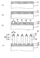
- FIGS. 4A to 4D are cross-sectional views schematically showing a manufacturing process of a semiconductor device of one embodiment according to the present invention.
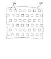
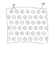
- FIGS. It is a figure which shows an example of the pattern of the opening part formed in a mask pattern. It is a figure which shows an example of the pattern of a nano column.
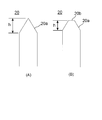
- (A), (B) is a figure which shows roughly the cross-sectional shape along the central axis of the front-end
- (B) is a figure which shows typically the structure of the front-end
- (A) to (F) are diagrams showing SEM images in a top view of nanocolumn groups regularly arranged in a triangular lattice shape.
- FIG 20 is a graph showing measurement results of light intensity distribution with respect to PL emission wavelength of the nanocolumn group in FIGS. 19A to 19F. It is a graph which shows the relationship between a column period and the light emission peak wavelength of the light intensity distribution of FIG. It is a figure which shows the SEM image in the top view of the nanocolumn group regularly arranged in the triangular lattice form.
- (A) is a figure which shows schematically a part of structure of the semiconductor light-emitting device of 2nd Embodiment, respectively. It is a perspective view which shows a part of structure of the semiconductor light-emitting device of the 3rd Embodiment concerning this invention. It is a perspective view which shows a part of structure of the semiconductor light-emitting device of the 3rd Embodiment concerning this invention.
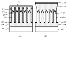
- FIG. 1A to 1D are cross-sectional views schematically showing a manufacturing process of a semiconductor optical device array 10 according to an embodiment of the present invention.
- FIG. 1D schematically shows the structure of the semiconductor optical device array 10 of the present embodiment.
- the semiconductor optical device array 10 has a template substrate, a mask pattern 13P having a plurality of openings, and a plurality of nanocolumns 23.
- the template substrate is a semiconductor substrate obtained by epitaxially growing a group III nitride semiconductor layer 12P on a base substrate 11 such as a sapphire substrate.
- a buffer layer (not shown) such as gallium nitride or aluminum nitride is grown on the underlying substrate 11 by a low temperature process by metal organic chemical vapor deposition (MOCVD: Metal-Organic-Chemical-Vapor-Deposition) method or MBE method.
- MOCVD Metal-Organic-Chemical-Vapor-Deposition
- a plurality of recesses 14,..., 14 are formed on the main surface on the surface side of the group III nitride semiconductor layer 12P.
- Mask pattern 13P is formed on the main surface of group III nitride semiconductor layer 12P, and has openings (hereinafter referred to as mask openings) immediately above the plurality of recesses 14,. ing. That is, the recess 14 is formed such that the opening is covered with the recess 14 and the recess 14 is exposed from the opening.
- the semiconductor optical device array 10 includes a semiconductor element (nanocolumn 23) including a fine columnar crystal 20, an active layer 21 provided on the fine columnar crystal 20, and a semiconductor coating layer 22 covering the active layer 21. ).
- the plurality of columnar crystals 20,..., 20 are made of a group III nitride semiconductor grown from the recesses 14,..., 14 of the group III nitride semiconductor layer 12P toward the upper side of the mask pattern 13P through the mask openings. .
- An active layer 21 is formed on the fine columnar crystal 20, and a semiconductor coating layer 22 that covers the active layer 21 is further formed.
- a nanocolumn 23 is constituted by the fine columnar crystal 20, the active layer 21 and the semiconductor coating layer 22.
- the fine columnar crystal 20 and the semiconductor coating layer 22 are made of a group III nitride semiconductor such as gallium nitride (GaN).
- the fine columnar crystal 20 and the semiconductor coating layer 22 are represented by the general formula Al x Ga y In 1-xy N (0 ⁇ x ⁇ 1, 0 ⁇ y ⁇ 1, and 0 ⁇ x + y ⁇ 1).
- a quaternary mixed crystal material or boron nitride may be used.
- the quaternary mixed crystal material has a wide band gap of 0.63 eV to 6.2 eV at room temperature depending on the composition ratios x and y.
- a light-emitting diode or a laser diode that covers the outside light region can be manufactured.
- the fine columnar crystal 20 preferably has a diameter of 10 nm or more and 1000 nm or less. Especially, it is preferable that it is 700 nm or less, Furthermore, 650 nm or less, More preferably, it is 600 nm or less. If the thickness is 700 nm or less, particularly 600 nm or less, the occurrence of threading dislocations can be easily suppressed.
- the diameter of the fine columnar crystal 20 is the diameter of the columnar portion 201 exposed from the mask opening.
- the diameter of the columnar part 201 is the diameter when the columnar part 201 is cylindrical.
- the columnar part 201 passes through the center of gravity (plane center) when viewed in plan from the substrate surface side of the semiconductor substrate, and between the intersections among the straight lines intersecting the columnar part 201 at two points. The length of the straight line with the longest distance.
- the fine columnar crystal 20 includes a columnar portion 201 and a facet structure 202 provided at the tip of the columnar portion 201.
- the shape of the columnar part 201 is not particularly limited, but may be, for example, a cylindrical shape, a quadrangular column shape, a hexagonal column shape, or the like.
- the fine columnar crystal 20 is preferably made of a material having a crystal structure of hexagonal crystal from the viewpoint of manufacturing stability.
- the active layer 21 is provided so as to cover the facet structure 202 of the fine columnar crystal 20.
- the active layer 21 is made of, for example, InGaN, GaN, AlGaN, AlInGaN, InGaAsN, or InN.
- the active layer 21 includes, for example, InGaN / GaN (barrier layer: InGaN, well layer: GaN), In x Ga 1-x N / In y Ga 1-y N (0 ⁇ x ⁇ 1, 0 ⁇ y ⁇ 1), GaN / AlGaN (barrier layer: AlGaN, well layer: GaN), or Al x Ga 1-x N / Al y Ga 1-y N (0 ⁇ x ⁇ 1, 0 ⁇ y ⁇ 1) It is only necessary to have a multiple quantum well (MQW) structure or a single quantum well (SQW) structure.
- the quantum well structure includes a quantum well layer and a barrier layer sandwiching the quantum well layer. The band gap of the barrier layer is larger than that of the quantum well layer.
- the semiconductor coating layer 22 is provided on the active layer 21 and completely covers the active layer 21.
- the peak wavelength of light emitted from the active layer 21 can be set to a wavelength corresponding to the diameter ⁇ of the fine columnar crystal 20 immediately before the active layer 21 is formed.
- the peak wavelength of the light emitted from the active layer 21 shifts to the longer wavelength side as the diameter ⁇ of each fine columnar crystal 20 is larger, and shifts to the shorter wavelength side as the diameter ⁇ of each fine columnar crystal 20 is smaller. It is possible to determine. That is, the peak wavelength of light emitted from the active layer 21 on the fine columnar crystal 20 having a large diameter ⁇ is longer than the peak wavelength of light emitted from the active layer 21 on the fine columnar crystal 20 having a small diameter ⁇ . It is.
- a desired emission wavelength can be obtained by controlling the diameter ⁇ of the fine columnar crystal 20.
- the diameter ⁇ of the fine columnar crystal 20 is set to a desired value by adjusting the diameter ⁇ (FIG. 1C) of each recess 14 formed in the group III nitride semiconductor layer 12P of the template substrate. can do. Since the diameter ⁇ of the recess 14 depends on the size of the mask opening, if the size of the mask opening is determined in advance, the diameter ⁇ corresponding to this size can be obtained.
- the peak wavelength of the light emitted from the active layer 21 can be set to a wavelength according to the surface area of the tip (facet structure 202) of the fine columnar crystal 20 of each nanocolumn 23.
- the peak wavelength of the light emitted from the active layer 21 can be determined so that it shifts to the longer wavelength side as the surface area of the facet structure is larger, and shifts to the shorter wavelength side as the surface area of the facet structure is smaller. That is, the peak wavelength of light emitted from the active layer 21 on the fine columnar crystal 20 having a large surface area of the facet structure is the peak wavelength of light emitted from the active layer 21 on the fine columnar crystal 20 having a small surface area of the facet structure. Longer wavelength. Therefore, it is possible to obtain a desired emission wavelength by controlling the surface area of the facet structure at the tip of the fine columnar crystal 20.
- the openings 13g,..., 13g formed in the mask pattern 13P are periodically arranged in the in-plane direction of the mask pattern 13P.
- a region having a high arrangement density of the plurality of openings and a region having a low arrangement density of the plurality of openings are formed in the mask pattern, a plurality of fine patterns in the region having a high arrangement density of the openings are formed.
- the peak wavelength of light emitted from the active layer 21 on the columnar crystal 20 is longer than the peak wavelength of light emitted from the active layer 21 on the plurality of fine columnar crystals 20 in the region where the arrangement density of the openings is low. Wavelength.
- the peak wavelength of the light emitted from the active layer 21 shifts to the longer wavelength side as the in-plane density of the fine columnar crystals 20,..., 20 increases, and the in-plane density of the fine columnar crystals 20,. It can be determined that the lower the value is, the shorter the wavelength is shifted.
- the in-plane density increases as the spatial period of the fine columnar crystals 20,... 20 decreases, or increases as the diameter of the fine columnar crystal 20 increases.
- a buffer layer such as gallium nitride or aluminum nitride is grown on the base substrate 11 by a low temperature process by MOCVD or MBE, and a group III nitride such as gallium nitride or aluminum nitride is formed on the buffer layer.
- the physical semiconductor layer 12 is grown (FIG. 1A).
- a template substrate including the substrate 11 and the group III nitride semiconductor layer 12 is manufactured.
- a metal mask layer 13 containing titanium (Ti) is formed in a predetermined region of the main surface of the template substrate (FIG. 1B).
- the metal mask layer 13 may be a natural oxide film of titanium or a titanium oxide film.
- the constituent material of the metal mask layer 13 is preferably titanium in that the fine columnar crystals 20 are selectively grown.
- the material is not limited to this, and titanium (Ti), tantalum (Ta), iron (Fe), nickel ( It may include one or more metals selected from the group consisting of Ni), platinum (Pt), gold (Au), cobalt (Co), tungsten (W), and molybdenum (Mo).
- the metal mask layer 13 is patterned to form a mask pattern 13P having a plurality of openings exposing the surface of the group III nitride semiconductor layer 12P, as shown in FIG.
- This patterning can be performed by a lithography process. That is, a mask pattern 13P can be formed by forming a resist pattern on the metal mask layer 13 and executing etching using the resist pattern as an etching mask. Alternatively, the mask pattern 13P can be formed by irradiating the metal mask layer 13 with a predetermined dose amount (irradiation ion amount per unit area) using a FIB (Focused Ion Beam) method.
- FIB Fluorused Ion Beam
- the top view shape of the opening of the mask pattern 13P (that is, the top view shape of the concave portion 14) is not particularly limited, and in addition to the square shape shown in FIG. But you can.
- the fine columnar crystal 20, the active layer 21 and the semiconductor coating layer 22 are continuously grown from the plurality of recesses 14 through the mask openings to the upper side of the mask pattern 13P by MOCVD or MBE (FIG. 1D )).
- the fine columnar crystal 20 grows above the mask pattern 13P and at the same time grows in the lateral direction along the in-plane direction of the template substrate. Therefore, the diameter ⁇ of the nanocolumn 23 is larger than the diameter ⁇ of the recess 14.
- the semiconductor coating layer 22 is formed so as to completely cover the active layer 21, the active layer 21 does not have an exposed portion to the external space. In other words, the active layer 21 is completely embedded in the tip of the nanocolumn 23.
- the fine columnar crystal 20 By reducing the mask opening diameter, the occurrence of threading dislocations at the initial growth stage of the fine columnar crystal 20 is suppressed. If the diameter is then increased by lateral growth, a relatively large diameter fine columnar crystal (for example, a diameter of 1000 nm) without threading dislocations can be obtained.
- a method of relatively increasing the nitrogen supply amount for example, a method of using AlGaN, and the like.
- the shape of the top view is a hexagon.
- 4A and 4B are diagrams schematically showing a cross-sectional shape along the central axis of the tip portion of the fine columnar crystal 20.
- the tip portion shown in FIG. 4A has a facet structure, and has an inclined surface formed of a semipolar surface 20a of a wurtzite crystal structure as a facet surface facing obliquely upward.
- the tip has a hexagonal pyramid shape.
- the tip portion shown in FIG. 4B also has a facet structure, but as a facet surface facing obliquely upward and a surface facing directly upward, from the semipolar surface 20a of the wurtzite crystal structure. And a flat polar surface 20b.
- the facet structure is a polyhedron structure having a facet surface located obliquely with respect to the horizontal plane of the base substrate 11 as a side surface.
- the diameter of the fine columnar crystal 20 is small, a tip portion having a hexagonal pyramid shape as shown in FIG. 4A is easily formed. If the diameter of the fine columnar crystal 20 is large, the tip as shown in FIG. The part is easy to be formed.
- a flat polar surface 20b can clearly appear at the tip of the fine columnar crystal 20. Further, as the diameter of the fine columnar crystal 20 increases beyond about 300 nm, the area of the flat polar surface 20b increases.
- the fine columnar crystal 20 is grown using the MBE method
- the fine columnar crystal 20 is grown by introducing a source gas containing active nitrogen and group III metal generated by high frequency plasma excitation onto the surface of the template substrate.
- the growth conditions at this time may be such that the effective columnar crystal 20 is grown by increasing the effective supply ratio of active nitrogen as compared with the group III metal.
- the fine columnar crystal 20 made of gallium nitride (GaN) is grown, if the crystal growth temperature is set to 600 ° C. or less, the GaN crystal often grows in a growth suppression region other than the mask opening.
- the higher the growth temperature the smaller the spatial density of the GaN crystal that grows in the growth suppression region.
- the temperature at which GaN is not grown in the growth suppression region is 850 ° C. or more as an example, although it depends on the supply amount and ratio of the group III metal and active nitrogen.
- MBE is desirably performed under the following conditions.
- the temperature is appropriately selected according to the type of group III nitride semiconductor to be grown, but is in the range of 350 ° C. or higher and 1200 ° C. or lower.
- the temperature is appropriately selected according to the type of group III nitride semiconductor to be grown, but is in the range of 350 ° C. or higher and 1200 ° C. or lower.
- the group III nitride semiconductor fine columnar crystal 20 can be grown.
- the region on the mask pattern 13P where the mask opening is not formed is a region where the growth of the fine columnar crystal 20 is suppressed (growth suppression region).
- growth suppression region a region where the growth of the fine columnar crystal 20 is suppressed.
- the surface of the metal film is irradiated with active nitrogen alone or simultaneously with the group III metal.
- a metal having a nitride forming ability it is estimated that a metal nitride (for example, TiN, WN) is formed. Since these metal nitrides are chemically stable, that is, there are few active dangling bonds on the surface, bonding with Ga, GaN, etc. is weak. Therefore, when the growth temperature is sufficient for Ga, GaN, etc. to desorb from the surface, the supplied Ga, GaN, etc. will be desorbed before it becomes large enough to sustain crystal growth. It is thought that growth is suppressed.
- the reason why lateral crystal growth is suppressed in the growth suppression region is that, in particular, the temperature in the growth suppression region is higher than that of the substrate surface, and GaN growth nuclei are hardly formed on the growth suppression region. Synergistic effects with points are expected.
- the fine columnar crystal 20 formed on the surface of the template substrate and the mask pattern 13P can change depending on the material of the template substrate and the mask pattern 13P, the film thickness of the mask pattern 13P, or the growth conditions. It grows upright in a direction substantially perpendicular to the surface or the surface of the mask pattern 13P.
- the fine columnar crystal 20 made of a group III nitride semiconductor grown by the method of this embodiment is a single crystal having a columnar structure having a diameter ⁇ in the nanometer order.
- the diameter of the fine columnar crystal 20 is set to a size within a range of 10 nm to 1000 nm, for example.
- the height of the fine columnar crystal 20 may vary depending on the thickness of the mask pattern 13P and the crystal growth conditions, but is, for example, in the range of 0.2 ⁇ m to 5 ⁇ m.
- the thickness of the mask pattern 13P is not particularly limited, but is preferably in the range of 2 nm to 100 nm. However, the diameter and height of the fine columnar crystal 20 may vary depending on crystal growth conditions.
- an active layer 21 is provided on each fine columnar crystal 20, and a semiconductor coating layer 22 is formed on the active layer 21.
- the active layer 21 and the semiconductor coating layer 22 can be formed by the MOCVD method or the MBE method.
- the material constituting the active layer 21 and the semiconductor coating layer 22 is also deposited on the mask pattern 13P. Further, when forming the semiconductor coating layer 22, it is preferable to grow it in the lateral direction so as to cover not only the upper surface of the active layer 21 but also the side surfaces.
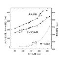
- FIG. 5 is a graph showing the relationship between the diameter (hereinafter referred to as “hole diameter”) ⁇ of the recess 14 formed in the group III nitride semiconductor layer 12P and the emission wavelength of the nanocolumn 23.
- the manufacturing conditions of the nanocolumn 23 produced to obtain the graph of FIG. 5 are as follows.
- a GaN layer 12P (thickness: about 3.5 ⁇ m) was grown on the (0001) surface of the sapphire substrate 11 by the MOCVD method to form a template substrate.
- the FIB method is used to form a plurality of openings arranged in a triangular lattice pattern (space period (between the centers of the openings)).
- 400 nm to form a mask pattern 13P.
- a recess 14 was formed in the GaN layer 12P.
- a GaN columnar crystal 20 (height: 2.5 ⁇ m) was grown from the concave portion 14 of the template substrate through the mask opening by the RF-MBE method at a temperature of 900 ° C. Subsequently, an active layer 21 having a multiple quantum well structure including an InGaN film (thickness: 1 nm) was formed on each fine columnar crystal 20. Subsequently, a GaN crystal semiconductor coating layer 22 (thickness: 10 nm) was formed on the active layer 21.
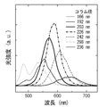
- FIG. 6 shows the PL emission wavelength (unit: nm) and light intensity (unit: arbitrary unit) measured for each of the semiconductor elements having nanocolumn diameters of 166 nm, 192 nm, 203 nm, 226 nm, 242 nm, 298 nm, and 236 nm. It is a graph which shows the relationship between.
- the manufacturing conditions of the nanocolumn 23 produced to obtain this graph are the same as the manufacturing conditions of the nanocolumn 23 produced to obtain the graph of FIG.
- FIG. 7 is a graph showing the relationship between the nanocolumn diameter (Nanocolumn Size) and the detected peak wavelength (Peak Wavelength). It can be seen that the larger the nanocolumn diameter, the longer the peak wavelength, and the smaller the nanocolumn diameter, the shorter the peak wavelength.
- the peak wavelength shifts to the longer wavelength side as the diameter ⁇ of the fine columnar crystal 20 just before the active layer 21 is formed, and shifts to the shorter wavelength side as the diameter ⁇ of the fine columnar crystal 20 decreases.
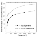
- FIG. 8 shows the dose amount (Doze (cm ⁇ 2 )) and the depth (Nanohole depth (nm)) of the concave portion 14 when the concave portion (hole) 14 is formed in the template substrate using the FIB method. It is a graph which shows a relationship.
- FIG. 9 shows the relationship between the dose (Doze (cm ⁇ 2 )) and the diameter (Nanohole size (nm)) ⁇ of the recess 14, and the dose (Doze (cm ⁇ 2 )) and the diameter of the nanocolumn 23. It is a graph which shows the relationship with (Nanocolumn size (nm)).
- the manufacturing conditions of the nanocolumn 23 produced to obtain the graphs of FIGS. 8 and 9 are as follows.
- a GaN layer 12P (thickness: about 3.5 ⁇ m) was grown on the (0001) surface of the sapphire substrate 11 by the MOCVD method to form a template substrate.
- a mask pattern 13P was formed by providing a plurality of mask openings in this titanium thin film using the FIB method. Concurrently with the formation of the mask opening, a recess 14 was formed in the GaN layer 12P.
- a GaN columnar crystal 20 (height: 2.5 ⁇ m) was grown from the concave portion 14 of the template substrate through the mask opening by the RF-MBE method at a temperature of 900 ° C. Subsequently, an active layer 21 having a multiple quantum well structure including an InGaN film (thickness: 1 nm) was formed on each fine columnar crystal 20. Subsequently, a GaN crystal semiconductor coating layer 22 (thickness: 10 nm) was formed on the active layer 21.
- the depth of the concave portion 14 increases as the dose amount when the focused ion beam is irradiated onto the metal mask layer 13 increases. Further, as shown in the graph of FIG. 9, it can be seen that the larger the dose amount, the larger the diameter (nanohole (size) of the recess 14 and the larger the diameter (nanocolumn size) of the nanocolumn 23. Therefore, it is understood that the diameter ⁇ of the fine columnar crystal 20 increases as the diameter of the recess 14 increases.
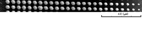
- FIG. 10 and 11 are diagrams showing scanning electron microscope images (SEM images) of nanocolumns 23,..., 23 having different diameters regularly arranged in a square lattice shape.
- FIG. 10 shows an SEM image of the nanocolumns 23,..., 23 as viewed from above
- FIG. 11 is an SEM image when the nanocolumns 23,.
- the nanocolumn group shown in FIG. 10 and FIG. 11 was produced by individually controlling the diameters of the recesses 14.
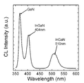
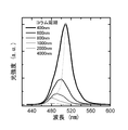
- FIG. 12 is a graph showing the measurement results of the spectrum of CL (cathode luminescence) light emitted from the nanocolumn 23.
- the horizontal axis of this graph corresponds to the emission wavelength
- the vertical axis of the graph corresponds to the CL intensity (arbitrary unit).
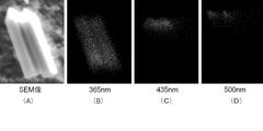
- FIG. 13A shows an SEM image of the nanocolumn 23 as viewed from above
- FIGS. 13B and 13C are top views of CL images (cathode luminescence images) having different wavelengths of 405 nm and 510 nm, respectively.
- 14A shows SEM images obtained by imaging the nanocolumn 23 from the lateral direction
- FIG. 14 shows the cross section CL image of the nano column 23 of (A).
- the manufacturing conditions for the nanocolumns 23 produced to obtain FIGS. 12, 13A to 13C, and FIGS. 14A to 14D are as follows.
- a GaN layer 12P (thickness: about 3.5 ⁇ m) was grown on the (0001) surface of the sapphire substrate 11 by the MOCVD method to form a template substrate.
- a plurality of openings (spatial period: 400 nm) arranged in a triangular lattice shape are provided in the titanium thin film by using the FIB method.
- a mask pattern 13P was formed. Concurrently with the formation of the mask opening, a recess 14 was formed in the GaN layer 12P.
- a GaN columnar crystal 20 (height 1.8 ⁇ m, diameter 180 to 495 nm) was grown from the recess 14 of the template substrate through the mask opening by the RF-MBE method at a temperature of 900 ° C. Subsequently, an active layer 21 having a multiple quantum well structure including an InGaN film (thickness: 3 nm) was formed on each fine columnar crystal 20. Subsequently, a GaN crystal semiconductor coating layer 22 (thickness: 10 nm) was formed on the active layer 21.
- the CL intensity distribution has a peak of emission from GaN and two peaks of emission from InGaN (wavelengths: 404 nm and 510 nm).
- a CL image with a wavelength of 405 nm shown in FIG. 13B shows light emission from the entire active layer 21 of the nanocolumn 23.
- This CL image is considered to indicate light emission from InGaN formed on the side surface (semipolar surface) 20a (FIG. 4B) of the tip of the fine columnar crystal 20.
- a CL image with a wavelength of 510 nm shown in FIG. 13C shows light emission only from the vicinity of the top of the active layer 21 of the nanocolumn 23.
- This CL image is considered to indicate light emission from InGaN formed on the flat surface (polar surface) 20b (FIG. 4B) at the tip of the fine columnar crystal 20.
- a cross-sectional CL image with a wavelength of 365 nm shown in FIG. 14B shows light emission from GaN distributed throughout the nanocolumn 23.
- a cross-sectional CL image having a wavelength of 435 nm shown in FIG. 14C shows light emission from InGaN at the entire tip of the nanocolumn 23.
- This cross-sectional CL image is considered to mainly indicate light emission from InGaN formed on the side surface (semipolar surface) 20a (FIG. 4B) of the tip of the fine columnar crystal 20.
- a cross-sectional CL image with a wavelength of 500 nm shown in FIG. 14D shows light emission from InGaN near the top of the nanocolumn 23.
- This cross-sectional CL image is considered to mainly indicate light emission from InGaN formed on the flat surface (polar surface) 20 b (FIG. 4B) at the tip of the fine columnar crystal 20.
- the InGaN formed on the side surface (semipolar surface) 20a of the tip of the fine columnar crystal 20 is formed.
- the emission wavelength is different from the emission wavelength of InGaN formed on the flat surface (polar surface) 20b of the tip. The reason is considered as follows.
- the InGaN crystal 21s formed on the side surface 20a of the fine columnar crystal 20 and the InGaN crystal 21t formed on the flat surface 20b can easily incorporate In into the InGaN crystal. Therefore, it is considered that the In composition ratio in the InGaN crystal 21t formed on the flat surface 20b is relatively high, and the In composition ratio in the InGaN crystal 21s formed on the side surface 20a is relatively low. For this reason, the CL spectrum (same CL spectrum as FIG. 12) shown in FIG. 15A is formed. Moreover, since the carriers are confined in the InGaN crystal 21t having a narrow band gap near the tip, the InGaN crystal 21t near the tip can form a quantum dot. This is considered to cause a difference between the emission wavelength of InGaN formed on the side surface 20a and the emission wavelength of InGaN formed on the flat surface 20b.
- PL (photoluminescence) intensity was measured using a sample prepared to obtain the CL intensity distribution of FIG. CW (Continuous Wave) light having a wavelength of 405 nm was used as excitation light.
- the excitation light density was 0.29 kW / cm 2 .
- the peak wavelength of the PL intensity distribution is 486.2 nm at a low temperature condition of 4K and 486.7 nm at a high temperature condition of 300K, and the full width at half maximum (FWHM) of the PL intensity distribution is at a low temperature condition of 4K. This corresponds to 151.3 meV, and corresponds to 187.2 meV at a high temperature condition of 300K.
- the PL integral intensity ratio between the low temperature condition and the high temperature condition that is, the internal quantum efficiency was about 77% with respect to the wavelength of 486 nm, and very good crystallinity was confirmed.
- One reason why such a high internal quantum efficiency is realized is that the exposed portion of the active layer 21 (21s, 21t) is not exposed to the external space, and the loss of injected carriers due to non-radiative recombination is suppressed. It is done.
- the InGaN crystals 21 s and 21 t having a narrow band gap are completely covered with GaN having a wide band gap and are embedded in the nanocolumns 23.
- the exposed portions of the InGaN crystals 21s and 21t to the external space are eliminated, it can be considered that the formation of non-radiative recombination levels is suppressed. If there is an exposed portion, a non-radiative recombination level is formed in the band gap on the surface of the exposed portion, and light is emitted by recombination of electrons and holes through this non-radiative recombination level. Efficiency is reduced.
- the nanocolumn 23 having the InGaN crystals 21s and 21t is mentioned here, the InGaN crystal 21t may not be provided. Even in such a nanocolumn, it has been confirmed that the emission wavelength can be controlled by the diameter of the nanocolumn. That is, it has been confirmed that the peak wavelength of light emitted from the nanocolumn active layer having a small diameter is lower than the peak wavelength of light emitted from the active layer on the nanocolumn having a large diameter.
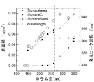
- FIG. 16 is a graph showing the relationship between the diameter of the nanocolumn 23 (column diameter) and the surface area of the facet structure at the tip of the nanocolumn 23 and the relationship between the column diameter and the emission peak wavelength.
- the emission peak wavelength is a wavelength detected from the intensity distribution of PL light.
- the symbol “ ⁇ ” indicates the measured value of the emission peak wavelength
- the symbol “ ⁇ ” indicates the area of the flat surface (SurfaceC) of the tip of the nanocolumn 23
- the symbol “ ⁇ ” indicates the inclined side surface of the tip of the nanocolumn 23
- the area “SurfaceSemi” indicates the area of the flat surface of the tip of the nanocolumn 23 and the area of the inclined side surface.
- the manufacturing conditions of the nanocolumn 23 produced to obtain the graph of FIG. 16 are as follows.
- a GaN layer 12P (thickness: about 3.5 ⁇ m) was grown on the (0001) surface of the sapphire substrate 11 by the MOCVD method to form a template substrate.
- a plurality of openings (spatial period: 400 nm) arranged in a triangular lattice shape are provided in the titanium thin film by using the FIB method.
- a mask pattern 13P was formed.
- a recess 14 was formed in the GaN layer 12P.
- a GaN columnar crystal 20 (height: 2.5 ⁇ m) was grown from the concave portion 14 of the template substrate through the mask opening by the RF-MBE method at a temperature of 900 ° C. Subsequently, an active layer 21 having a multiple quantum well structure including an InGaN film (thickness: 1 nm) was formed on each fine columnar crystal 20. Subsequently, a GaN crystal semiconductor coating layer 22 (thickness: 10 nm) was formed on the active layer 21.
- FIG. 16 is a graph showing the measurement results.
- the surface area of the facet structure at the tip of the nanocolumn 23 increases.
- the value of the emission peak wavelength monotonously increases as the column diameter increases. Therefore, the value of the emission peak wavelength increases with an increase in the total area of the facet surfaces facing upward in the tip portion of the nanocolumn 23. Since the film thickness of the active layer 21 and the film thickness of the semiconductor coating layer 22 are thin, the emission peak wavelength is substantially increased with an increase in the area of the facet surface facing upward in the tip of the fine columnar crystal 20. Can do. Therefore, it is possible to obtain a desired emission peak wavelength by controlling the area of the facet surface facing upward in the tip portion of the fine columnar crystal 20.
- the value of the emission peak wavelength increases as the area of the inclined side surface (SurfaceSemi) at the tip of the nanocolumn 23 increases.
- the column diameter exceeds about 260 nm, this correlation does not hold.
- the value of the emission peak wavelength increases as the area of the flat surface (Surface C) at the tip of the nanocolumn 23 increases.
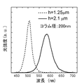
- FIG. 17 is a graph showing a light intensity distribution (unit: arbitrary unit) regarding the PL emission wavelength of the nanocolumn 23 having a column diameter of 200 nm.
- the solid line indicates the measurement curve when the height h of the inclined side surface of the tip of the nanocolumn 23 is 2.1 ⁇ m
- the broken line indicates the height h of the inclined side surface of the tip of the nanocolumn 23 is 1.25 ⁇ m.
- the measurement curves are shown respectively.
- FIG. 18 is a graph showing the relationship between the height h and the emission peak wavelength for the same nanocolumn 23.
- the horizontal axis of the graph in FIG. 18 corresponds to the height h
- the vertical axis corresponds to the emission peak wavelength.
- the manufacturing conditions of the nanocolumn 23 produced to obtain the graphs of FIGS. 17 and 18 are as follows.
- a GaN layer 12P (thickness: about 3.5 ⁇ m) was grown on the (0001) surface of the sapphire substrate 11 by the MOCVD method to form a template substrate.
- a plurality of openings (spatial period: 400 nm) arranged in a triangular lattice shape are provided in the titanium thin film by using the FIB method.
- a mask pattern 13P was formed.
- a recess 14 was formed in the GaN layer 12P.
- a GaN columnar crystal 20 (height: 2.5 ⁇ m) was grown from the concave portion 14 of the template substrate through the mask opening by the RF-MBE method at a temperature of 900 ° C. Subsequently, an active layer 21 having a multiple quantum well structure including an InGaN film (thickness: 1 nm) was formed on each fine columnar crystal 20. Subsequently, a GaN crystal semiconductor coating layer 22 (thickness: 10 nm) was formed on the active layer 21.
- FIG. 17 when the height h of the inclined side surface of the tip of the nanocolumn 23 is changed from 1.25 ⁇ m to 2.1 ⁇ m, the peak of the light intensity distribution is also shifted to the long wavelength side.
- FIG. 18 also shows this tendency.
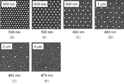
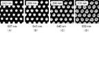
- FIGS. 19A to 19F are views showing SEM images of the nanocolumn group regularly arranged in a triangular lattice shape in a top view.
- 19 (A), (B), (C), (D), (E), and (F) are respectively the spatial period (distance between the centers of the fine columnar crystals 20) 400 nm, 600 nm, 800 nm, and 1 ⁇ m. , 2 ⁇ m, 4 ⁇ m.
- the peak wavelengths of PL emission corresponding to the arrays having a spatial period of 400 nm, 600 nm, 800 nm, 1 ⁇ m, 2 ⁇ m, and 4 ⁇ m were measured as 508 nm, 500 nm, 490 nm, 480 nm, 480 nm, and 479 nm, respectively.
- the manufacturing conditions of the nanocolumn 23 produced in order to obtain the SEM image of FIG. 19 are as follows.
- a GaN layer 12P (thickness: about 3.5 ⁇ m) was grown on the (0001) surface of the sapphire substrate 11 by the MOCVD method to form a template substrate.
- a plurality of mask openings (diameter of each mask opening: arranged in a triangular lattice pattern) on the titanium thin film using the FIB method. 167 nm) to form a mask pattern 13P.
- a recess 14 was formed in the GaN layer 12P.
- a GaN columnar crystal 20 (height 1.5 ⁇ m, diameter 190 nm) was grown from the concave portion 14 of the template substrate through the mask opening by the RF-MBE method at a temperature of 900 ° C. Subsequently, an active layer 21 having a multiple quantum well structure including an InGaN film (thickness: 3 nm) was formed on each fine columnar crystal 20. Subsequently, a GaN crystal semiconductor coating layer 22 (thickness: 10 nm) was formed on the active layer 21.
- the peak wavelength shifts to the longer wavelength side as the spatial period (column period, arrangement density) of the nanocolumns 23,... , 23 is shifted to the shorter wavelength side as the spatial period is longer.
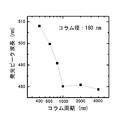
- FIG. 20 is a graph showing the measurement results of the light intensity distribution (unit: arbitrary unit) related to the PL emission wavelength of the nanocolumn group in FIGS. 19 (A) to 19 (F).
- FIG. 21 is a graph showing the relationship between the column period and the emission peak wavelength of the light intensity distribution of FIG.
- the column diameter of each nanocolumn 23 was set to 160 nm.
- the value of the emission peak wavelength decreases as the column period increases. If the column period is increased while the column diameter is kept constant, the in-plane density of the nanocolumns 23,..., 23 decreases, so that the emission peak wavelength decreases as the in-plane density decreases, and the emission peak wavelength increases as the in-plane density increases. become longer.
- FIG. 22 is a view showing an SEM image of the nanocolumn group regularly arranged in a triangular lattice shape in a top view.
- 22A, 22B, 22C, and 22D show arrangements in the case of spatial periods 242 nm, 269 nm, 298 nm, and 336 nm, respectively.
- the peak wavelengths of PL emission corresponding to the arrangement of spatial periods 242 nm, 269 nm, 298 nm, and 336 nm were measured as 607 nm, 643 nm, 649 nm, and 650 nm, respectively.
- the manufacturing conditions of the nanocolumns 23 produced to obtain the SEM images of FIGS. 22A to 22D are the same as those of the nanocolumns 23 produced to obtain the SEM images of FIG. 19 except for the diameter of the mask opening. The manufacturing conditions are the same.
- the diameter of the nanocolumn 23 produced to obtain the SEM image of FIG. 22 was set so as to increase as the spatial period increased.
- the value of the peak wavelength increases as the diameter of the nanocolumn 23 increases.
- the in-plane density (arrangement density) of the nanocolumns 23,..., 23 increases, so that the emission peak wavelength increases with the increase of the in-plane density and Shorter.
- the peak wavelength of light emitted from the active layer 21 is the fine columnar crystal 20,.
- the semiconductor optical device array 10 can control the position of the fine columnar crystal 20 formed on the template substrate by adjusting the position of the opening of the mask pattern 13P. it can.
- the diameter of the fine columnar crystal 20 can be controlled by adjusting the diameter of the concave portion 14 immediately below each opening, and thereby the peak wavelength of light emitted from the active layer 21 can be set to a desired wavelength. It is. Further, the diameter of each fine columnar crystal 20 can be increased to shift the peak wavelength to the longer wavelength side, and the diameter of each fine columnar crystal 20 can be decreased to shift the peak wavelength to the shorter wavelength side.
- the peak wavelength of the light emitted from the active layer 21 can be set to a desired wavelength.
- the surface area of the facet structure can be increased to shift the peak wavelength to the longer wavelength side, and the surface area of the facet structure can be decreased to shift the peak wavelength to the shorter wavelength side.
- the peak wavelength is shifted to the long wavelength side, and the in-plane density of the fine columnar crystals 20,.
- the in-plane density is controlled by adjusting the spatial period of the fine columnar crystals 20,..., 20 (that is, the spatial period of the openings formed in the mask pattern 13P), or the diameter of each fine columnar crystal 20 (that is, the mask). It can be performed with high accuracy by adjusting the diameter of the opening formed in the pattern 13P.
- FIGS. 23A and 23B are views each schematically showing a part of the configuration of the semiconductor light emitting device of the second embodiment.
- the structures shown in FIGS. 23A and 23B include the structure of the semiconductor optical device array 10 of the first embodiment.
- the group III nitride semiconductor layer 12P formed on the base substrate 11 is an n-type semiconductor layer into which an n-type impurity is introduced.
- Mask pattern 13P is connected to an n-side electrode (not shown).
- a fine columnar crystal 20 including an n-type cladding layer such as n-type AlGaN, an active layer 21, and a p-type semiconductor layer 24 including a p-type cladding layer such as p-type AlGaN.
- a nanocolumn consisting of An insulating film 30 such as silicon oxide is embedded in the space between these nanocolumns.
- a p-side electrode 31 such as a Ni / Au multilayer film or ITO (Indium Tin Oxide) is formed so as to be electrically connected to the p-type semiconductor layers 24,.
- the active layer 21 emits light when the holes injected from the p-side electrode and the electrons from the n-side electrode recombine in the active layer 21.
- the fine columnar crystal 20 is composed of an n-type semiconductor layer, and may have a three-layer structure of GaN / AlGaN / GaN, for example.
- the group III nitride semiconductor layer 12P formed on the base substrate 11 is an n-type semiconductor layer into which an n-type impurity is introduced.
- Mask pattern 13P is connected to an n-side electrode (not shown).
- a nanocolumn 23 is formed.
- the p-type semiconductor layer 25 is continuously formed in the lateral direction by promoting the crystal growth in the lateral direction.
- a p-side electrode 32 such as a Ni / Au multilayer film or ITO (Indium Tin Oxide) is formed so as to be electrically connected to the p-type semiconductor layer 25.
- the active layer 21 emits light when the holes injected from the p-side electrode and the electrons from the n-side electrode recombine in the active layer 21.
- an optical resonator for confining light emitted from the active layer 21 may be formed.
- multilayer reflectors can be formed above and below the active layer 21, respectively, and an optical resonator can be configured with these multilayer reflectors.
- An optical waveguide can also be formed in the p-type semiconductor layer 25.
- the structure in FIG. 23A or FIG. 23B can be modified into a photoelectric conversion element such as a solar cell.
- a pin structure (light absorption structure) may be formed instead of the active layer 21.
- the i-type semiconductor layer can have a quantum dot structure. Conversion efficiency can be improved by laminating a plurality of quantum dot layers via an intermediate layer to form an i-type semiconductor layer.
- the pin structure can be adapted to a desired absorption wavelength by controlling the diameter of the fine columnar crystal 20, the in-plane density of the fine columnar crystals 20, ..., or the tip shape of the fine columnar crystal 20. It is.
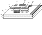
- FIGS. 24 and 25 are perspective views showing a part of the configuration of the semiconductor light emitting device of the third embodiment.
- the semiconductor light emitting device of the third embodiment includes the structure of the semiconductor optical device array 10 of the first embodiment.
- the group III nitride semiconductor layer 12P formed on the base substrate 11 is an n-type semiconductor layer into which an n-type impurity is introduced.
- An n-side electrode 40 is formed on the mask pattern 13P.
- a plurality of types of nanocolumn groups 23R, 23G, and 23B having different emission wavelengths are formed on the group III nitride semiconductor layer 12P.
- the nanocolumns constituting the nanocolumn groups 23R, 23G, and 23B include an n-type (first conductivity type) fine columnar crystal 20 including an n-type cladding layer such as n-type AlGaN, as shown in FIG.
- each of the nanocolumn groups 23R, 23G, and 23B has a crystal structure that emits light of wavelengths of three primary colors of R (red), G (green), and B (blue), respectively.
- p-type semiconductor layers 25R, 25G, and 25B are formed on the nanocolumn groups 23R, 23G, and 23B, respectively. Then, p-side electrodes 42R, 42G, and 42B are connected to the p-type semiconductor layers 25R, 25G, and 25B, respectively.
- the p-side electrodes 42R, 42G, and 42B may be made of a Ni / Au multilayer film or ITO (Indium Tin Oxide).
- the active layer can emit light by recombining holes injected from the p-side electrodes 42R, 42G, and 42B and electrons from the n-side electrode in the active layers of the nanocolumn groups 23R, 23G, and 23B.
- an optical resonator for confining light emitted from the active layer may be formed.
- multilayer reflectors can be formed above and below the active layer, respectively, and an optical resonator can be configured with these multilayer reflectors.
- the semiconductor light emitting device of the third embodiment can integrate light emitters that emit light of three primary colors on the same substrate 11. Furthermore, the light intensity distribution is controlled by individually adjusting the in-plane density of the nanocolumn groups 23R, 23G, and 23B that emit light of R, G, and B, respectively, and the entire spectrum distribution is changed to the spectrum distribution of sunlight. It is possible to approximate. As a result, an ideal white light emitting diode can be produced.
- a sapphire substrate is used as the base substrate 11, but the present invention is not limited to this.
- a silicon substrate or a SiC substrate may be used.
- a group III nitride semiconductor substrate such as a gallium nitride substrate may be used.
- the semiconductor optical element array according to the present invention can be applied in the fields of electronic devices and optical devices. Fine columnar crystals have excellent light-emitting properties and are expected to be applied to light-emitting devices.
- the semiconductor optical element array according to the present invention can be applied to, for example, a phosphor, a light emitting diode, a laser diode, or a photoelectric conversion element.
Landscapes
- Engineering & Computer Science (AREA)
- Chemical & Material Sciences (AREA)
- Physics & Mathematics (AREA)
- Computer Hardware Design (AREA)
- Power Engineering (AREA)
- Condensed Matter Physics & Semiconductors (AREA)
- General Physics & Mathematics (AREA)
- Manufacturing & Machinery (AREA)
- Microelectronics & Electronic Packaging (AREA)
- Nanotechnology (AREA)
- Crystallography & Structural Chemistry (AREA)
- Materials Engineering (AREA)
- Life Sciences & Earth Sciences (AREA)
- Biophysics (AREA)
- Optics & Photonics (AREA)
- Led Devices (AREA)
- Physical Deposition Of Substances That Are Components Of Semiconductor Devices (AREA)
- Crystals, And After-Treatments Of Crystals (AREA)
- Photovoltaic Devices (AREA)
Priority Applications (4)
| Application Number | Priority Date | Filing Date | Title |
|---|---|---|---|
| CN200980141161.XA CN102187479B (zh) | 2008-09-01 | 2009-08-27 | 半导体光学元件阵列及其制造方法 |
| EP09809577.1A EP2333847B1 (en) | 2008-09-01 | 2009-08-27 | Semiconductor optical element array and manufacturing method therefore |
| JP2010526554A JP5547076B2 (ja) | 2008-09-01 | 2009-08-27 | 半導体光素子アレイおよびその製造方法 |
| US13/061,425 US9224595B2 (en) | 2008-09-01 | 2009-08-27 | Semiconductor optical element array and method of manufacturing the same |
Applications Claiming Priority (4)
| Application Number | Priority Date | Filing Date | Title |
|---|---|---|---|
| JP2008-224131 | 2008-09-01 | ||
| JP2008224131 | 2008-09-01 | ||
| JP2008-224129 | 2008-09-01 | ||
| JP2008224129 | 2008-09-01 |
Publications (1)
| Publication Number | Publication Date |
|---|---|
| WO2010023921A1 true WO2010023921A1 (ja) | 2010-03-04 |
Family
ID=41721104
Family Applications (1)
| Application Number | Title | Priority Date | Filing Date |
|---|---|---|---|
| PCT/JP2009/004173 Ceased WO2010023921A1 (ja) | 2008-09-01 | 2009-08-27 | 半導体光素子アレイおよびその製造方法 |
Country Status (7)
| Country | Link |
|---|---|
| US (1) | US9224595B2 (enExample) |
| EP (1) | EP2333847B1 (enExample) |
| JP (2) | JP5547076B2 (enExample) |
| KR (1) | KR101567121B1 (enExample) |
| CN (1) | CN102187479B (enExample) |
| TW (1) | TWI470828B (enExample) |
| WO (1) | WO2010023921A1 (enExample) |
Cited By (37)
| Publication number | Priority date | Publication date | Assignee | Title |
|---|---|---|---|---|
| WO2011117056A1 (de) * | 2010-03-25 | 2011-09-29 | Osram Opto Semiconductors Gmbh | Strahlungsemittierendes halbleiterbauelement und verfahren zur herstellung eines strahlungsemittierenden halbleiterbauelements |
| KR20120028104A (ko) * | 2010-09-14 | 2012-03-22 | 삼성엘이디 주식회사 | Ⅲ족 질화물 나노로드 발광소자 및 그 제조 방법 |
| WO2012076901A1 (en) * | 2010-12-09 | 2012-06-14 | The University Of Nottingham | Electrical device |
| JP2014060198A (ja) * | 2012-09-14 | 2014-04-03 | Oki Electric Ind Co Ltd | 窒化物半導体発光ダイオードの製造方法、及び窒化物半導体発光ダイオード |
| JP2014107441A (ja) * | 2012-11-28 | 2014-06-09 | Fujitsu Ltd | 太陽電池及びその製造方法 |
| JP2014533897A (ja) * | 2011-12-01 | 2014-12-15 | コミサリア ア レネルジィ アトミーク エ オ ゼネ ルジイ アルテアナティーフCommissariata L’Energie Atomique Et Aux Energies Alternatives | コア/シェル構造を有するナノワイヤを備えた光電子デバイス |
| JP2015512151A (ja) * | 2012-02-14 | 2015-04-23 | クナノ・アーベー | 窒化ガリウムナノワイヤに基づくエレクトロニクス |
| JP2016521459A (ja) * | 2013-04-26 | 2016-07-21 | オスラム オプト セミコンダクターズ ゲゼルシャフト ミット ベシュレンクテル ハフツングOsram Opto Semiconductors GmbH | 活性ゾーンを有する半導体積層体を円柱状構造上に備えた発光アセンブリ |
| JP2016527706A (ja) * | 2013-06-07 | 2016-09-08 | グロ アーベーGlo Ab | マルチカラーled及びその製造方法 |
| JP2017195305A (ja) * | 2016-04-21 | 2017-10-26 | 富士通株式会社 | 発光素子及びその製造方法 |
| WO2018062252A1 (ja) * | 2016-09-29 | 2018-04-05 | 日亜化学工業株式会社 | 発光素子 |
| JP2018142660A (ja) * | 2017-02-28 | 2018-09-13 | 学校法人上智学院 | 光デバイスおよび光デバイスの製造方法 |
| JP2018206861A (ja) * | 2017-05-31 | 2018-12-27 | セイコーエプソン株式会社 | 発光装置、プロジェクター、および発光装置の製造方法 |
| JP2019012744A (ja) * | 2017-06-29 | 2019-01-24 | 学校法人 名城大学 | 半導体発光素子および半導体発光素子の製造方法 |
| JP2019525460A (ja) * | 2016-06-30 | 2019-09-05 | ヴァレオ ビジョンValeo Vision | 強化されたスペクトルを有する白色光を放射するモジュール |
| JP2020057640A (ja) * | 2018-09-28 | 2020-04-09 | セイコーエプソン株式会社 | 発光装置およびプロジェクター |
| JP2020077817A (ja) * | 2018-11-09 | 2020-05-21 | 学校法人 名城大学 | 半導体発光素子 |
| EP3696300A1 (de) | 2019-02-18 | 2020-08-19 | Aixatech GmbH | Verfahren zur herstellung eines verbundmaterialkörpers insbesondere für die verwendung bei der herstellung von elektronischen oder optoelektronischen bauelementen |
| JP2020141048A (ja) * | 2019-02-28 | 2020-09-03 | セイコーエプソン株式会社 | 発光装置およびプロジェクター |
| WO2022045206A1 (ja) * | 2020-08-31 | 2022-03-03 | 株式会社小糸製作所 | 半導体発光素子および半導体発光素子の製造方法 |
| JP2022052420A (ja) * | 2020-09-23 | 2022-04-04 | セイコーエプソン株式会社 | 発光装置、発光装置の製造方法およびプロジェクター |
| US11329190B2 (en) | 2019-03-26 | 2022-05-10 | Seiko Epson Corporation | Light emitting device and projector |
| JP2022526676A (ja) * | 2019-04-12 | 2022-05-25 | ラキシウム インコーポレイテッド | 同一基板上への異なる発光構造体の一体的な構成 |
| JP2022532642A (ja) * | 2019-05-14 | 2022-07-15 | オスラム オプト セミコンダクターズ ゲゼルシャフト ミット ベシュレンクテル ハフツング | 照明ユニット、照明ユニットの製造方法、光電子構造素子用の変換素子、ledと変換素子とを備えた放射源、光取り出し構造体、および光電子デバイス |
| JP2022118051A (ja) * | 2017-02-28 | 2022-08-12 | 学校法人上智学院 | 光デバイスおよび光デバイスの製造方法 |
| JPWO2022190353A1 (enExample) * | 2021-03-12 | 2022-09-15 | ||
| JP2022141079A (ja) * | 2021-03-15 | 2022-09-29 | セイコーエプソン株式会社 | 発光装置、プロジェクター、およびディスプレイ |
| US20220352415A1 (en) * | 2019-06-25 | 2022-11-03 | Aledia | Optoelectronic device comprising three-dimensional semiconductor elements and method for manufacturing said device |
| US11508874B2 (en) | 2019-11-28 | 2022-11-22 | Seiko Epson Corporation | Light emitting apparatus and projector |
| WO2022264854A1 (ja) * | 2021-06-14 | 2022-12-22 | 豊田合成株式会社 | 半導体発光素子の製造方法 |
| WO2023282177A1 (ja) * | 2021-07-08 | 2023-01-12 | 株式会社小糸製作所 | 半導体発光素子および半導体発光素子の製造方法 |
| JP2023010073A (ja) * | 2021-07-08 | 2023-01-20 | 株式会社小糸製作所 | 半導体発光素子および半導体発光素子の製造方法 |
| JP2023009782A (ja) * | 2021-07-08 | 2023-01-20 | 株式会社小糸製作所 | 半導体発光素子および半導体発光素子の製造方法 |
| JP2023041230A (ja) * | 2021-09-13 | 2023-03-24 | セイコーエプソン株式会社 | 発光装置およびプロジェクター |
| US11626533B2 (en) | 2019-03-26 | 2023-04-11 | Seiko Epson Corporation | Light emitting device and projector |
| JP2023527887A (ja) * | 2020-06-01 | 2023-06-30 | アレディア | 光電子デバイス及び光電子デバイスの製造方法 |
| KR20250044387A (ko) | 2022-08-02 | 2025-03-31 | 다이니폰 인사츠 가부시키가이샤 | 반도체 광소자 어레이 |
Families Citing this family (48)
| Publication number | Priority date | Publication date | Assignee | Title |
|---|---|---|---|---|
| CN103190005A (zh) * | 2010-11-04 | 2013-07-03 | 皇家飞利浦电子股份有限公司 | 基于结晶弛豫结构的固态发光器件 |
| SE537434C2 (sv) | 2012-06-26 | 2015-04-28 | Polar Light Technologies Ab | Grupp III-nitridstruktur |
| TWI476953B (zh) | 2012-08-10 | 2015-03-11 | Univ Nat Taiwan | 半導體發光元件及其製作方法 |
| EP2939276B1 (fr) * | 2012-12-28 | 2019-06-12 | Aledia | Dispositif opto-électronique à microfils ou nanofils |
| FR3000612B1 (fr) | 2012-12-28 | 2016-05-06 | Commissariat Energie Atomique | Dispositif optoelectronique a microfils ou nanofils |
| WO2014138904A1 (en) * | 2013-03-14 | 2014-09-18 | The Royal Institution For The Advancement Of Learning/Mcgill University | Methods and devices for solid state nanowire devices |
| KR102190675B1 (ko) * | 2013-10-10 | 2020-12-15 | 삼성전자주식회사 | 반도체 소자의 미세 패턴 형성 방법 |
| FR3023410A1 (fr) * | 2014-07-02 | 2016-01-08 | Aledia | Dispositif optoelectronique a elements semiconducteurs et son procede de fabrication |
| FR3026564B1 (fr) * | 2014-09-30 | 2018-02-16 | Commissariat A L'energie Atomique Et Aux Energies Alternatives | Dispositif optoelectronique a elements semiconducteurs tridimensionnels |
| KR102212557B1 (ko) | 2014-11-03 | 2021-02-08 | 삼성전자주식회사 | 나노구조 반도체 발광소자 |
| DE102014116999B4 (de) * | 2014-11-20 | 2025-09-18 | OSRAM Opto Semiconductors Gesellschaft mit beschränkter Haftung | Verfahren zur Herstellung eines optoelektronischen Halbleiterchips |
| FR3029015B1 (fr) * | 2014-11-24 | 2018-03-02 | Commissariat A L'energie Atomique Et Aux Energies Alternatives | Dispositif optoelectronique a elements semiconducteurs tridimensionnels et son procede de fabrication |
| DE102016104616B4 (de) * | 2016-03-14 | 2021-09-23 | OSRAM Opto Semiconductors Gesellschaft mit beschränkter Haftung | Halbleiterlichtquelle |
| FR3050322B1 (fr) * | 2016-04-18 | 2019-01-25 | Centre National De La Recherche Scientifique (Cnrs) | Dispositif photorecepteur multicouche, a parametres de maille differents |
| JP6972665B2 (ja) | 2017-05-31 | 2021-11-24 | セイコーエプソン株式会社 | 発光装置、プロジェクター、および発光装置の製造方法 |
| FR3068517B1 (fr) * | 2017-06-30 | 2019-08-09 | Aledia | Dispositif optoelectronique comportant des structures semiconductrices tridimensionnelles en configuration axiale |
| US10263151B2 (en) * | 2017-08-18 | 2019-04-16 | Globalfoundries Inc. | Light emitting diodes |
| CN107482094A (zh) * | 2017-09-21 | 2017-12-15 | 山西飞虹微纳米光电科技有限公司 | 基于GaN基轴向纳米棒阵列的LED及其制备方法 |
| JP7053209B2 (ja) * | 2017-10-02 | 2022-04-12 | 株式会社小糸製作所 | 半導体成長用基板、半導体素子、半導体発光素子及び半導体成長用基板の製造方法 |
| TW201938491A (zh) * | 2018-02-01 | 2019-10-01 | 日商日立化成股份有限公司 | 奈米結晶膜的製造方法 |
| CN109148651B (zh) * | 2018-08-06 | 2019-10-15 | 复旦大学 | 基于GaN条纹模板的多色发光InGaN量子阱外延片的制备方法 |
| JP7105442B2 (ja) | 2018-08-06 | 2022-07-25 | セイコーエプソン株式会社 | 発光装置およびプロジェクター |
| JP7188690B2 (ja) * | 2018-08-22 | 2022-12-13 | セイコーエプソン株式会社 | プロジェクター |
| KR102652501B1 (ko) | 2018-09-13 | 2024-03-29 | 삼성디스플레이 주식회사 | 발광 소자의 제조방법 및 발광 소자를 포함하는 표시 장치 |
| CN111463659B (zh) * | 2019-01-21 | 2021-08-13 | 华为技术有限公司 | 量子点半导体光放大器及其制备方法 |
| US20220102583A1 (en) * | 2019-01-29 | 2022-03-31 | Osram Opto Semiconductors Gmbh | µ-LED, µ-LED DEVICE, DISPLAY AND METHOD FOR THE SAME |
| JP7207012B2 (ja) | 2019-02-27 | 2023-01-18 | セイコーエプソン株式会社 | 発光装置の製造方法、発光装置、およびプロジェクター |
| JP6981444B2 (ja) | 2019-04-01 | 2021-12-15 | セイコーエプソン株式会社 | 発光装置、発光装置の製造方法、およびプロジェクター |
| RU2758776C2 (ru) * | 2019-12-05 | 2021-11-01 | Федеральное государственное бюджетное учреждение науки Физико-технический институт им. А.Ф. Иоффе Российской академии наук | Способ изготовления наноколончатой гетероструктуры на основе соединений iii-n |
| US11404473B2 (en) | 2019-12-23 | 2022-08-02 | Lumileds Llc | III-nitride multi-wavelength LED arrays |
| US11923398B2 (en) | 2019-12-23 | 2024-03-05 | Lumileds Llc | III-nitride multi-wavelength LED arrays |
| US11581450B2 (en) * | 2020-06-11 | 2023-02-14 | Globalfoundries U.S. Inc. | Photodiode and/or pin diode structures with one or more vertical surfaces |
| US20230335400A1 (en) * | 2020-06-22 | 2023-10-19 | Kyocera Corporation | Method for producing semiconductor device, semiconductor device, electronic device, method for producing semiconductor epitaxial substrate, and semiconductor epitaxial substrate |
| JP7176700B2 (ja) * | 2020-07-31 | 2022-11-22 | セイコーエプソン株式会社 | 発光装置およびプロジェクター |
| US11094846B1 (en) | 2020-08-31 | 2021-08-17 | 4233999 Canada Inc. | Monolithic nanocolumn structures |
| US11322649B2 (en) * | 2020-09-15 | 2022-05-03 | Applied Materials, Inc. | Three color light sources integrated on a single wafer |
| FR3114682B1 (fr) * | 2020-09-29 | 2023-05-19 | Aledia | Dispositif optoelectronique a diodes electroluminescentes a affichage couleur |
| JP7203390B2 (ja) | 2020-10-13 | 2023-01-13 | セイコーエプソン株式会社 | 発光装置およびプロジェクター |
| US11631786B2 (en) | 2020-11-12 | 2023-04-18 | Lumileds Llc | III-nitride multi-wavelength LED arrays with etch stop layer |
| JP7560829B2 (ja) * | 2020-11-20 | 2024-10-03 | セイコーエプソン株式会社 | 発光装置およびプロジェクター |
| JP7635545B2 (ja) * | 2020-12-18 | 2025-02-26 | セイコーエプソン株式会社 | 発光装置およびプロジェクター |
| JP7613127B2 (ja) | 2021-01-22 | 2025-01-15 | セイコーエプソン株式会社 | 発光装置、プロジェクター |
| JP7707605B2 (ja) * | 2021-03-29 | 2025-07-15 | セイコーエプソン株式会社 | 発光装置、プロジェクター、およびディスプレイ |
| JP2023065945A (ja) * | 2021-10-28 | 2023-05-15 | セイコーエプソン株式会社 | 発光装置およびプロジェクター |
| JP7272412B1 (ja) | 2021-12-03 | 2023-05-12 | 信越半導体株式会社 | 接合型半導体ウェーハの製造方法 |
| CN114300580B (zh) * | 2021-12-30 | 2024-06-04 | 长春理工大学 | 一种探测器材料及其制备方法 |
| US11799054B1 (en) | 2023-02-08 | 2023-10-24 | 4233999 Canada Inc. | Monochromatic emitters on coalesced selective area growth nanocolumns |
| WO2024164078A1 (en) * | 2023-02-08 | 2024-08-15 | 4233999 Canada Inc. | Light emitters on coalesced selective area growth nanocolumns |
Citations (5)
| Publication number | Priority date | Publication date | Assignee | Title |
|---|---|---|---|---|
| JP2003282942A (ja) * | 2001-08-22 | 2003-10-03 | Sony Corp | 窒化物半導体素子及び窒化物半導体素子の製造方法 |
| WO2006025407A1 (ja) * | 2004-08-31 | 2006-03-09 | Akihiko Kikuchi | 発光素子及びその製造方法 |
| JP2007027298A (ja) * | 2005-07-14 | 2007-02-01 | Matsushita Electric Works Ltd | 半導体発光素子およびそれを用いる照明装置ならびに半導体発光素子の製造方法 |
| JP2008022014A (ja) * | 2006-07-13 | 2008-01-31 | Sharp Corp | 窒化物半導体を加工してなる発光デバイスの処理方法 |
| JP2008108924A (ja) | 2006-10-26 | 2008-05-08 | Matsushita Electric Works Ltd | 化合物半導体発光素子およびそれを用いる照明装置ならびに化合物半導体発光素子の製造方法 |
Family Cites Families (20)
| Publication number | Priority date | Publication date | Assignee | Title |
|---|---|---|---|---|
| DE69220824T2 (de) | 1991-03-22 | 1998-01-29 | Hitachi Ltd | Optische Halbleitervorrichtung |
| JP4780113B2 (ja) | 2000-09-18 | 2011-09-28 | 三菱化学株式会社 | 半導体発光素子 |
| JP3556916B2 (ja) * | 2000-09-18 | 2004-08-25 | 三菱電線工業株式会社 | 半導体基材の製造方法 |
| JP4381397B2 (ja) | 2000-10-04 | 2009-12-09 | 三洋電機株式会社 | 窒化物系半導体素子および窒化物系半導体の形成方法 |
| JP3863720B2 (ja) * | 2000-10-04 | 2006-12-27 | 三洋電機株式会社 | 窒化物系半導体素子および窒化物系半導体の形成方法 |
| JP3679720B2 (ja) * | 2001-02-27 | 2005-08-03 | 三洋電機株式会社 | 窒化物系半導体素子および窒化物系半導体の形成方法 |
| JP3454791B2 (ja) * | 2001-03-01 | 2003-10-06 | 三洋電機株式会社 | 窒化物系半導体素子および窒化物系半導体の形成方法 |
| CN1241272C (zh) * | 2001-08-22 | 2006-02-08 | 索尼公司 | 氮化物半导体器件及其制造方法 |
| DE10213643A1 (de) | 2002-03-27 | 2003-10-09 | Geka Brush Gmbh | Kosmetikeinheit |
| US7485902B2 (en) * | 2002-09-18 | 2009-02-03 | Sanyo Electric Co., Ltd. | Nitride-based semiconductor light-emitting device |
| US6936851B2 (en) * | 2003-03-21 | 2005-08-30 | Tien Yang Wang | Semiconductor light-emitting device and method for manufacturing the same |
| JP2004354617A (ja) * | 2003-05-28 | 2004-12-16 | Sharp Corp | フォトニック結晶とその製造方法 |
| US7132677B2 (en) | 2004-02-13 | 2006-11-07 | Dongguk University | Super bright light emitting diode of nanorod array structure having InGaN quantum well and method for manufacturing the same |
| JP2006339534A (ja) | 2005-06-03 | 2006-12-14 | Sony Corp | 発光ダイオード、発光ダイオードの製造方法、発光ダイオードバックライト、発光ダイオード照明装置、発光ダイオードディスプレイおよび電子機器 |
| MX2008011275A (es) * | 2006-03-10 | 2008-11-25 | Stc Unm | Crecimiento pulsado de nanoalambres de gan y aplicaciones en materiales y dispositivos de substrato semiconductor de nitruros del grupo iii. |
| JP2008034482A (ja) * | 2006-07-26 | 2008-02-14 | Matsushita Electric Works Ltd | 化合物半導体発光素子およびそれを用いる照明装置ならびに化合物半導体素子の製造方法 |
| JP2008034483A (ja) | 2006-07-26 | 2008-02-14 | Matsushita Electric Works Ltd | 化合物半導体素子およびそれを用いる照明装置ならびに化合物半導体素子の製造方法 |
| WO2008034823A1 (en) * | 2006-09-18 | 2008-03-27 | Qunano Ab | Method of producing precision vertical and horizontal layers in a vertical semiconductor structure |
| JP2008108757A (ja) * | 2006-10-23 | 2008-05-08 | Matsushita Electric Works Ltd | 化合物半導体発光素子およびそれを用いる照明装置ならびに化合物半導体素子の製造方法 |
| US8030108B1 (en) * | 2008-06-30 | 2011-10-04 | Stc.Unm | Epitaxial growth of in-plane nanowires and nanowire devices |
-
2009
- 2009-08-27 EP EP09809577.1A patent/EP2333847B1/en active Active
- 2009-08-27 US US13/061,425 patent/US9224595B2/en active Active
- 2009-08-27 KR KR1020117007423A patent/KR101567121B1/ko not_active Expired - Fee Related
- 2009-08-27 JP JP2010526554A patent/JP5547076B2/ja active Active
- 2009-08-27 CN CN200980141161.XA patent/CN102187479B/zh active Active
- 2009-08-27 WO PCT/JP2009/004173 patent/WO2010023921A1/ja not_active Ceased
- 2009-09-01 TW TW98129403A patent/TWI470828B/zh not_active IP Right Cessation
-
2013
- 2013-06-24 JP JP2013132114A patent/JP5687731B2/ja not_active Expired - Fee Related
Patent Citations (5)
| Publication number | Priority date | Publication date | Assignee | Title |
|---|---|---|---|---|
| JP2003282942A (ja) * | 2001-08-22 | 2003-10-03 | Sony Corp | 窒化物半導体素子及び窒化物半導体素子の製造方法 |
| WO2006025407A1 (ja) * | 2004-08-31 | 2006-03-09 | Akihiko Kikuchi | 発光素子及びその製造方法 |
| JP2007027298A (ja) * | 2005-07-14 | 2007-02-01 | Matsushita Electric Works Ltd | 半導体発光素子およびそれを用いる照明装置ならびに半導体発光素子の製造方法 |
| JP2008022014A (ja) * | 2006-07-13 | 2008-01-31 | Sharp Corp | 窒化物半導体を加工してなる発光デバイスの処理方法 |
| JP2008108924A (ja) | 2006-10-26 | 2008-05-08 | Matsushita Electric Works Ltd | 化合物半導体発光素子およびそれを用いる照明装置ならびに化合物半導体発光素子の製造方法 |
Non-Patent Citations (5)
| Title |
|---|
| H. SEKIGUCHI ET AL., JOURNAL OF CRYSTAL GROWTH, vol. 300, 2007, pages 259 - 262 |
| H. SEKIGUCHI, T. NAKAZATO, A. KIKUCHI, K. KISHINO: "Structural and optical properties of GaN nanocolumns grown on (0001) sapphire substrates by rf-plasma-assisted molecular-beam epitaxy", JOURNAL OF CRYSTAL GROWTH, vol. 300, 2007, pages 259 - 262 |
| M. YOSHIZAWA ET AL., JPN. J. APPL. PHYS., vol. 36, no. 4B, 1997, pages L459 - L462 |
| M. YOSHIZAWA, A. KIKUCHI, M. MORI, N. FUJITA, K. KISHINO: "Growth of Self-Organized GaN Nanostructures on A1203 (0001) by RF-Radical Source Molecular Beam Epitaxy", JPN. J. APPL. PHYS., vol. 36, no. 4B, 1997, pages L459 - L462 |
| See also references of EP2333847A4 |
Cited By (64)
| Publication number | Priority date | Publication date | Assignee | Title |
|---|---|---|---|---|
| WO2011117056A1 (de) * | 2010-03-25 | 2011-09-29 | Osram Opto Semiconductors Gmbh | Strahlungsemittierendes halbleiterbauelement und verfahren zur herstellung eines strahlungsemittierenden halbleiterbauelements |
| US9024294B2 (en) | 2010-09-14 | 2015-05-05 | Samsung Electronics Co., Ltd. | Group III nitride nanorod light emitting device |
| KR20120028104A (ko) * | 2010-09-14 | 2012-03-22 | 삼성엘이디 주식회사 | Ⅲ족 질화물 나노로드 발광소자 및 그 제조 방법 |
| CN102403428A (zh) * | 2010-09-14 | 2012-04-04 | 三星Led株式会社 | Ⅲ族氮化物纳米棒发光装置及其制造方法 |
| KR101710159B1 (ko) * | 2010-09-14 | 2017-03-08 | 삼성전자주식회사 | Ⅲ족 질화물 나노로드 발광소자 및 그 제조 방법 |
| WO2012076901A1 (en) * | 2010-12-09 | 2012-06-14 | The University Of Nottingham | Electrical device |
| JP2014533897A (ja) * | 2011-12-01 | 2014-12-15 | コミサリア ア レネルジィ アトミーク エ オ ゼネ ルジイ アルテアナティーフCommissariata L’Energie Atomique Et Aux Energies Alternatives | コア/シェル構造を有するナノワイヤを備えた光電子デバイス |
| US10236178B2 (en) | 2012-02-14 | 2019-03-19 | Hexagem Ab | Gallium nitride nanowire based electronics |
| US9653286B2 (en) | 2012-02-14 | 2017-05-16 | Hexagem Ab | Gallium nitride nanowire based electronics |
| JP2015512151A (ja) * | 2012-02-14 | 2015-04-23 | クナノ・アーベー | 窒化ガリウムナノワイヤに基づくエレクトロニクス |
| JP2014060198A (ja) * | 2012-09-14 | 2014-04-03 | Oki Electric Ind Co Ltd | 窒化物半導体発光ダイオードの製造方法、及び窒化物半導体発光ダイオード |
| JP2014107441A (ja) * | 2012-11-28 | 2014-06-09 | Fujitsu Ltd | 太陽電池及びその製造方法 |
| JP2016521459A (ja) * | 2013-04-26 | 2016-07-21 | オスラム オプト セミコンダクターズ ゲゼルシャフト ミット ベシュレンクテル ハフツングOsram Opto Semiconductors GmbH | 活性ゾーンを有する半導体積層体を円柱状構造上に備えた発光アセンブリ |
| US9531161B2 (en) | 2013-04-26 | 2016-12-27 | Osram Opto Semiconductors Gmbh | Light-emitting assembly having a semiconductor layer sequence having an active zone on a columnar structure |
| JP2016527706A (ja) * | 2013-06-07 | 2016-09-08 | グロ アーベーGlo Ab | マルチカラーled及びその製造方法 |
| US9748437B2 (en) | 2013-06-07 | 2017-08-29 | Glo Ab | Multicolor LED and method of fabricating thereof |
| US10304992B2 (en) | 2013-06-07 | 2019-05-28 | Glo Ab | Multicolor LED and method of fabricating thereof |
| JP2017195305A (ja) * | 2016-04-21 | 2017-10-26 | 富士通株式会社 | 発光素子及びその製造方法 |
| JP2019525460A (ja) * | 2016-06-30 | 2019-09-05 | ヴァレオ ビジョンValeo Vision | 強化されたスペクトルを有する白色光を放射するモジュール |
| JPWO2018062252A1 (ja) * | 2016-09-29 | 2019-06-24 | 日亜化学工業株式会社 | 発光素子 |
| US11482642B2 (en) | 2016-09-29 | 2022-10-25 | Nichia Corporation | Light emitting element |
| WO2018062252A1 (ja) * | 2016-09-29 | 2018-04-05 | 日亜化学工業株式会社 | 発光素子 |
| US10879422B2 (en) | 2016-09-29 | 2020-12-29 | Nichia Corporation | Light emitting element |
| JP2022118051A (ja) * | 2017-02-28 | 2022-08-12 | 学校法人上智学院 | 光デバイスおよび光デバイスの製造方法 |
| JP2018142660A (ja) * | 2017-02-28 | 2018-09-13 | 学校法人上智学院 | 光デバイスおよび光デバイスの製造方法 |
| JP7090861B2 (ja) | 2017-02-28 | 2022-06-27 | 学校法人上智学院 | 光デバイスおよび光デバイスの製造方法 |
| JP7333666B2 (ja) | 2017-02-28 | 2023-08-25 | 学校法人上智学院 | 光デバイスおよび光デバイスの製造方法 |
| JP2018206861A (ja) * | 2017-05-31 | 2018-12-27 | セイコーエプソン株式会社 | 発光装置、プロジェクター、および発光装置の製造方法 |
| JP7147132B2 (ja) | 2017-05-31 | 2022-10-05 | セイコーエプソン株式会社 | 発光装置、プロジェクター、および発光装置の製造方法 |
| JP2019012744A (ja) * | 2017-06-29 | 2019-01-24 | 学校法人 名城大学 | 半導体発光素子および半導体発光素子の製造方法 |
| JP7320770B2 (ja) | 2018-09-28 | 2023-08-04 | セイコーエプソン株式会社 | 発光装置およびプロジェクター |
| JP2020057640A (ja) * | 2018-09-28 | 2020-04-09 | セイコーエプソン株式会社 | 発光装置およびプロジェクター |
| JP7312997B2 (ja) | 2018-11-09 | 2023-07-24 | 学校法人 名城大学 | 半導体発光素子 |
| JP2020077817A (ja) * | 2018-11-09 | 2020-05-21 | 学校法人 名城大学 | 半導体発光素子 |
| EP3696300A1 (de) | 2019-02-18 | 2020-08-19 | Aixatech GmbH | Verfahren zur herstellung eines verbundmaterialkörpers insbesondere für die verwendung bei der herstellung von elektronischen oder optoelektronischen bauelementen |
| JP2020141048A (ja) * | 2019-02-28 | 2020-09-03 | セイコーエプソン株式会社 | 発光装置およびプロジェクター |
| JP7232461B2 (ja) | 2019-02-28 | 2023-03-03 | セイコーエプソン株式会社 | 発光装置およびプロジェクター |
| US11329190B2 (en) | 2019-03-26 | 2022-05-10 | Seiko Epson Corporation | Light emitting device and projector |
| US11626533B2 (en) | 2019-03-26 | 2023-04-11 | Seiko Epson Corporation | Light emitting device and projector |
| JP2022526676A (ja) * | 2019-04-12 | 2022-05-25 | ラキシウム インコーポレイテッド | 同一基板上への異なる発光構造体の一体的な構成 |
| US12191418B2 (en) | 2019-04-12 | 2025-01-07 | Google Llc | Monolithic integration of different light emitting structures on a same substrate |
| JP7534324B2 (ja) | 2019-04-12 | 2024-08-14 | グーグル エルエルシー | 同一基板上への異なる発光構造体の一体的な構成 |
| JP2022532642A (ja) * | 2019-05-14 | 2022-07-15 | オスラム オプト セミコンダクターズ ゲゼルシャフト ミット ベシュレンクテル ハフツング | 照明ユニット、照明ユニットの製造方法、光電子構造素子用の変換素子、ledと変換素子とを備えた放射源、光取り出し構造体、および光電子デバイス |
| US20220352415A1 (en) * | 2019-06-25 | 2022-11-03 | Aledia | Optoelectronic device comprising three-dimensional semiconductor elements and method for manufacturing said device |
| US11508874B2 (en) | 2019-11-28 | 2022-11-22 | Seiko Epson Corporation | Light emitting apparatus and projector |
| JP2023527887A (ja) * | 2020-06-01 | 2023-06-30 | アレディア | 光電子デバイス及び光電子デバイスの製造方法 |
| JP7520305B2 (ja) | 2020-08-31 | 2024-07-23 | 株式会社小糸製作所 | 半導体発光素子および半導体発光素子の製造方法 |
| WO2022045206A1 (ja) * | 2020-08-31 | 2022-03-03 | 株式会社小糸製作所 | 半導体発光素子および半導体発光素子の製造方法 |
| JP2022040676A (ja) * | 2020-08-31 | 2022-03-11 | 株式会社小糸製作所 | 半導体発光素子および半導体発光素子の製造方法 |
| JP7556246B2 (ja) | 2020-09-23 | 2024-09-26 | セイコーエプソン株式会社 | 発光装置、発光装置の製造方法およびプロジェクター |
| JP2022052420A (ja) * | 2020-09-23 | 2022-04-04 | セイコーエプソン株式会社 | 発光装置、発光装置の製造方法およびプロジェクター |
| JPWO2022190353A1 (enExample) * | 2021-03-12 | 2022-09-15 | ||
| WO2022190353A1 (ja) * | 2021-03-12 | 2022-09-15 | シャープ株式会社 | 量子ドット、量子ドット層、発光素子、及び太陽電池 |
| JP7594654B2 (ja) | 2021-03-12 | 2024-12-04 | シャープ株式会社 | 量子ドット、量子ドット層、発光素子、及び太陽電池 |
| JP7320794B2 (ja) | 2021-03-15 | 2023-08-04 | セイコーエプソン株式会社 | 発光装置、プロジェクター、およびディスプレイ |
| JP2022141079A (ja) * | 2021-03-15 | 2022-09-29 | セイコーエプソン株式会社 | 発光装置、プロジェクター、およびディスプレイ |
| WO2022264854A1 (ja) * | 2021-06-14 | 2022-12-22 | 豊田合成株式会社 | 半導体発光素子の製造方法 |
| JP2023009782A (ja) * | 2021-07-08 | 2023-01-20 | 株式会社小糸製作所 | 半導体発光素子および半導体発光素子の製造方法 |
| WO2023282177A1 (ja) * | 2021-07-08 | 2023-01-12 | 株式会社小糸製作所 | 半導体発光素子および半導体発光素子の製造方法 |
| JP2023010073A (ja) * | 2021-07-08 | 2023-01-20 | 株式会社小糸製作所 | 半導体発光素子および半導体発光素子の製造方法 |
| JP7758492B2 (ja) | 2021-07-08 | 2025-10-22 | 株式会社小糸製作所 | 半導体発光素子および半導体発光素子の製造方法 |
| JP7770123B2 (ja) | 2021-07-08 | 2025-11-14 | 株式会社小糸製作所 | 半導体発光素子および半導体発光素子の製造方法 |
| JP2023041230A (ja) * | 2021-09-13 | 2023-03-24 | セイコーエプソン株式会社 | 発光装置およびプロジェクター |
| KR20250044387A (ko) | 2022-08-02 | 2025-03-31 | 다이니폰 인사츠 가부시키가이샤 | 반도체 광소자 어레이 |
Also Published As
| Publication number | Publication date |
|---|---|
| TWI470828B (zh) | 2015-01-21 |
| JP2013239718A (ja) | 2013-11-28 |
| KR101567121B1 (ko) | 2015-11-06 |
| EP2333847B1 (en) | 2018-02-14 |
| US9224595B2 (en) | 2015-12-29 |
| JP5687731B2 (ja) | 2015-03-18 |
| CN102187479A (zh) | 2011-09-14 |
| KR20110063799A (ko) | 2011-06-14 |
| JP5547076B2 (ja) | 2014-07-09 |
| TW201027800A (en) | 2010-07-16 |
| EP2333847A4 (en) | 2015-02-25 |
| JPWO2010023921A1 (ja) | 2012-01-26 |
| US20110169025A1 (en) | 2011-07-14 |
| EP2333847A1 (en) | 2011-06-15 |
| CN102187479B (zh) | 2014-06-18 |
Similar Documents
| Publication | Publication Date | Title |
|---|---|---|
| JP5687731B2 (ja) | 半導体光素子アレイおよびその製造方法 | |
| US20170069793A1 (en) | Ultraviolet light-emitting device and production method therefor | |
| US20110220871A1 (en) | Nitride semiconductor light-emitting device and semiconductor light-emitting device | |
| US8791025B2 (en) | Method of producing microstructure of nitride semiconductor and photonic crystal prepared according to the method | |
| JP2009055016A (ja) | 半導体デバイスおよびその製造方法 | |
| KR20010081005A (ko) | 인듐-풍부 클러스터를 갖는 ⅲ-질화물 양자 웰 구조 및이의 제조 방법 | |
| JP5143214B2 (ja) | 半導体発光素子 | |
| KR20220066948A (ko) | 물질의 조성물 | |
| TW202425077A (zh) | 奈米結構/微結構裝置 | |
| US12419142B2 (en) | Nitride semiconductor ultraviolet light emitting element | |
| TWI828945B (zh) | 氮化物半導體紫外線發光元件 | |
| US12419139B2 (en) | Nitride semiconductor ultraviolet light-emitting element and production method therefor | |
| CN116114073A (zh) | 氮化物半导体紫外线发光元件 | |
| TW202107734A (zh) | 發光二極體及其製造方法 | |
| WO2024029553A1 (ja) | 半導体光素子アレイ | |
| TWI881114B (zh) | 氮化物半導體紫外線發光元件及其製造方法 | |
| JP2022118051A (ja) | 光デバイスおよび光デバイスの製造方法 | |
| JP5227870B2 (ja) | エピタキシャル基板、半導体素子構造、およびエピタキシャル基板の作製方法 | |
| JP2008117902A (ja) | 窒化物半導体素子の製造方法 | |
| Kishino et al. | Molecular beam epitaxial growth of GaN nanocolumns and related nanocolumn emitters | |
| JP2009253047A (ja) | Iii族窒化物発光素子及びエピタキシャルウエハ | |
| JP2020077832A (ja) | 半導体素子及び半導体レーザダイオード | |
| JP2013135016A (ja) | 窒化物半導体発光素子およびその製造方法 |
Legal Events
| Date | Code | Title | Description |
|---|---|---|---|
| WWE | Wipo information: entry into national phase |
Ref document number: 200980141161.X Country of ref document: CN |
|
| 121 | Ep: the epo has been informed by wipo that ep was designated in this application |
Ref document number: 09809577 Country of ref document: EP Kind code of ref document: A1 |
|
| WWE | Wipo information: entry into national phase |
Ref document number: 2010526554 Country of ref document: JP |
|
| WWE | Wipo information: entry into national phase |
Ref document number: 13061425 Country of ref document: US |
|
| NENP | Non-entry into the national phase |
Ref country code: DE |
|
| WWE | Wipo information: entry into national phase |
Ref document number: 2009809577 Country of ref document: EP |
|
| ENP | Entry into the national phase |
Ref document number: 20117007423 Country of ref document: KR Kind code of ref document: A |