WO2010018813A1 - 電荷輸送性ポリマー、有機電界発光素子用組成物、有機電界発光素子、有機elディスプレイ及び有機el照明 - Google Patents
電荷輸送性ポリマー、有機電界発光素子用組成物、有機電界発光素子、有機elディスプレイ及び有機el照明 Download PDFInfo
- Publication number
- WO2010018813A1 WO2010018813A1 PCT/JP2009/064134 JP2009064134W WO2010018813A1 WO 2010018813 A1 WO2010018813 A1 WO 2010018813A1 JP 2009064134 W JP2009064134 W JP 2009064134W WO 2010018813 A1 WO2010018813 A1 WO 2010018813A1
- Authority
- WO
- WIPO (PCT)
- Prior art keywords
- group
- formula
- layer
- charge transporting
- transporting polymer
- Prior art date
Links
- 0 CCC(CC1c2ccccc12)c(cc1)ccc1C1=CC=*C(C)C1 Chemical compound CCC(CC1c2ccccc12)c(cc1)ccc1C1=CC=*C(C)C1 0.000 description 3
- BQRFGQSTJCZGBK-UHFFFAOYSA-N CC(C)c(cc1)ccc1[IH]c1ccc(C)cc1 Chemical compound CC(C)c(cc1)ccc1[IH]c1ccc(C)cc1 BQRFGQSTJCZGBK-UHFFFAOYSA-N 0.000 description 1
- IYFZTPUGUAVDMF-UHFFFAOYSA-N CCCCCCC1(CCCCCC)c2cc([N]3(C4)C4C3)ccc2-c2ccc(CCCCN)cc12 Chemical compound CCCCCCC1(CCCCCC)c2cc([N]3(C4)C4C3)ccc2-c2ccc(CCCCN)cc12 IYFZTPUGUAVDMF-UHFFFAOYSA-N 0.000 description 1
- AASWSXXTMLHQER-UHFFFAOYSA-N Fc(c([B](c(c(F)c(c(F)c1F)F)c1F)(c(c(F)c(c(F)c1F)F)c1F)c(c(F)c(c(F)c1F)F)c1F)c(c(F)c1F)F)c1F Chemical compound Fc(c([B](c(c(F)c(c(F)c1F)F)c1F)(c(c(F)c(c(F)c1F)F)c1F)c(c(F)c(c(F)c1F)F)c1F)c(c(F)c1F)F)c1F AASWSXXTMLHQER-UHFFFAOYSA-N 0.000 description 1
Images
Classifications
-
- C—CHEMISTRY; METALLURGY
- C08—ORGANIC MACROMOLECULAR COMPOUNDS; THEIR PREPARATION OR CHEMICAL WORKING-UP; COMPOSITIONS BASED THEREON
- C08G—MACROMOLECULAR COMPOUNDS OBTAINED OTHERWISE THAN BY REACTIONS ONLY INVOLVING UNSATURATED CARBON-TO-CARBON BONDS
- C08G61/00—Macromolecular compounds obtained by reactions forming a carbon-to-carbon link in the main chain of the macromolecule
- C08G61/12—Macromolecular compounds containing atoms other than carbon in the main chain of the macromolecule
-
- C—CHEMISTRY; METALLURGY
- C08—ORGANIC MACROMOLECULAR COMPOUNDS; THEIR PREPARATION OR CHEMICAL WORKING-UP; COMPOSITIONS BASED THEREON
- C08G—MACROMOLECULAR COMPOUNDS OBTAINED OTHERWISE THAN BY REACTIONS ONLY INVOLVING UNSATURATED CARBON-TO-CARBON BONDS
- C08G73/00—Macromolecular compounds obtained by reactions forming a linkage containing nitrogen with or without oxygen or carbon in the main chain of the macromolecule, not provided for in groups C08G12/00 - C08G71/00
- C08G73/02—Polyamines
- C08G73/026—Wholly aromatic polyamines
-
- C—CHEMISTRY; METALLURGY
- C08—ORGANIC MACROMOLECULAR COMPOUNDS; THEIR PREPARATION OR CHEMICAL WORKING-UP; COMPOSITIONS BASED THEREON
- C08L—COMPOSITIONS OF MACROMOLECULAR COMPOUNDS
- C08L79/00—Compositions of macromolecular compounds obtained by reactions forming in the main chain of the macromolecule a linkage containing nitrogen with or without oxygen or carbon only, not provided for in groups C08L61/00 - C08L77/00
- C08L79/02—Polyamines
-
- H—ELECTRICITY
- H01—ELECTRIC ELEMENTS
- H01B—CABLES; CONDUCTORS; INSULATORS; SELECTION OF MATERIALS FOR THEIR CONDUCTIVE, INSULATING OR DIELECTRIC PROPERTIES
- H01B1/00—Conductors or conductive bodies characterised by the conductive materials; Selection of materials as conductors
- H01B1/06—Conductors or conductive bodies characterised by the conductive materials; Selection of materials as conductors mainly consisting of other non-metallic substances
- H01B1/12—Conductors or conductive bodies characterised by the conductive materials; Selection of materials as conductors mainly consisting of other non-metallic substances organic substances
- H01B1/124—Intrinsically conductive polymers
- H01B1/128—Intrinsically conductive polymers comprising six-membered aromatic rings in the main chain, e.g. polyanilines, polyphenylenes
-
- H—ELECTRICITY
- H10—SEMICONDUCTOR DEVICES; ELECTRIC SOLID-STATE DEVICES NOT OTHERWISE PROVIDED FOR
- H10K—ORGANIC ELECTRIC SOLID-STATE DEVICES
- H10K50/00—Organic light-emitting devices
- H10K50/10—OLEDs or polymer light-emitting diodes [PLED]
- H10K50/14—Carrier transporting layers
-
- H—ELECTRICITY
- H10—SEMICONDUCTOR DEVICES; ELECTRIC SOLID-STATE DEVICES NOT OTHERWISE PROVIDED FOR
- H10K—ORGANIC ELECTRIC SOLID-STATE DEVICES
- H10K85/00—Organic materials used in the body or electrodes of devices covered by this subclass
- H10K85/10—Organic polymers or oligomers
- H10K85/111—Organic polymers or oligomers comprising aromatic, heteroaromatic, or aryl chains, e.g. polyaniline, polyphenylene or polyphenylene vinylene
- H10K85/115—Polyfluorene; Derivatives thereof
-
- H—ELECTRICITY
- H10—SEMICONDUCTOR DEVICES; ELECTRIC SOLID-STATE DEVICES NOT OTHERWISE PROVIDED FOR
- H10K—ORGANIC ELECTRIC SOLID-STATE DEVICES
- H10K85/00—Organic materials used in the body or electrodes of devices covered by this subclass
- H10K85/10—Organic polymers or oligomers
- H10K85/151—Copolymers
-
- H—ELECTRICITY
- H10—SEMICONDUCTOR DEVICES; ELECTRIC SOLID-STATE DEVICES NOT OTHERWISE PROVIDED FOR
- H10K—ORGANIC ELECTRIC SOLID-STATE DEVICES
- H10K85/00—Organic materials used in the body or electrodes of devices covered by this subclass
- H10K85/30—Coordination compounds
- H10K85/321—Metal complexes comprising a group IIIA element, e.g. Tris (8-hydroxyquinoline) gallium [Gaq3]
- H10K85/324—Metal complexes comprising a group IIIA element, e.g. Tris (8-hydroxyquinoline) gallium [Gaq3] comprising aluminium, e.g. Alq3
-
- H—ELECTRICITY
- H10—SEMICONDUCTOR DEVICES; ELECTRIC SOLID-STATE DEVICES NOT OTHERWISE PROVIDED FOR
- H10K—ORGANIC ELECTRIC SOLID-STATE DEVICES
- H10K85/00—Organic materials used in the body or electrodes of devices covered by this subclass
- H10K85/60—Organic compounds having low molecular weight
- H10K85/615—Polycyclic condensed aromatic hydrocarbons, e.g. anthracene
-
- H—ELECTRICITY
- H10—SEMICONDUCTOR DEVICES; ELECTRIC SOLID-STATE DEVICES NOT OTHERWISE PROVIDED FOR
- H10K—ORGANIC ELECTRIC SOLID-STATE DEVICES
- H10K85/00—Organic materials used in the body or electrodes of devices covered by this subclass
- H10K85/60—Organic compounds having low molecular weight
- H10K85/631—Amine compounds having at least two aryl rest on at least one amine-nitrogen atom, e.g. triphenylamine
- H10K85/633—Amine compounds having at least two aryl rest on at least one amine-nitrogen atom, e.g. triphenylamine comprising polycyclic condensed aromatic hydrocarbons as substituents on the nitrogen atom
-
- C—CHEMISTRY; METALLURGY
- C08—ORGANIC MACROMOLECULAR COMPOUNDS; THEIR PREPARATION OR CHEMICAL WORKING-UP; COMPOSITIONS BASED THEREON
- C08G—MACROMOLECULAR COMPOUNDS OBTAINED OTHERWISE THAN BY REACTIONS ONLY INVOLVING UNSATURATED CARBON-TO-CARBON BONDS
- C08G2261/00—Macromolecular compounds obtained by reactions forming a carbon-to-carbon link in the main chain of the macromolecule
- C08G2261/10—Definition of the polymer structure
- C08G2261/14—Side-groups
- C08G2261/141—Side-chains having aliphatic units
-
- C—CHEMISTRY; METALLURGY
- C08—ORGANIC MACROMOLECULAR COMPOUNDS; THEIR PREPARATION OR CHEMICAL WORKING-UP; COMPOSITIONS BASED THEREON
- C08G—MACROMOLECULAR COMPOUNDS OBTAINED OTHERWISE THAN BY REACTIONS ONLY INVOLVING UNSATURATED CARBON-TO-CARBON BONDS
- C08G2261/00—Macromolecular compounds obtained by reactions forming a carbon-to-carbon link in the main chain of the macromolecule
- C08G2261/30—Monomer units or repeat units incorporating structural elements in the main chain
- C08G2261/31—Monomer units or repeat units incorporating structural elements in the main chain incorporating aromatic structural elements in the main chain
- C08G2261/316—Monomer units or repeat units incorporating structural elements in the main chain incorporating aromatic structural elements in the main chain bridged by heteroatoms, e.g. N, P, Si or B
- C08G2261/3162—Arylamines
-
- C—CHEMISTRY; METALLURGY
- C08—ORGANIC MACROMOLECULAR COMPOUNDS; THEIR PREPARATION OR CHEMICAL WORKING-UP; COMPOSITIONS BASED THEREON
- C08G—MACROMOLECULAR COMPOUNDS OBTAINED OTHERWISE THAN BY REACTIONS ONLY INVOLVING UNSATURATED CARBON-TO-CARBON BONDS
- C08G2261/00—Macromolecular compounds obtained by reactions forming a carbon-to-carbon link in the main chain of the macromolecule
- C08G2261/50—Physical properties
- C08G2261/51—Charge transport
- C08G2261/512—Hole transport
-
- C—CHEMISTRY; METALLURGY
- C08—ORGANIC MACROMOLECULAR COMPOUNDS; THEIR PREPARATION OR CHEMICAL WORKING-UP; COMPOSITIONS BASED THEREON
- C08G—MACROMOLECULAR COMPOUNDS OBTAINED OTHERWISE THAN BY REACTIONS ONLY INVOLVING UNSATURATED CARBON-TO-CARBON BONDS
- C08G2261/00—Macromolecular compounds obtained by reactions forming a carbon-to-carbon link in the main chain of the macromolecule
- C08G2261/70—Post-treatment
- C08G2261/76—Post-treatment crosslinking
-
- H—ELECTRICITY
- H10—SEMICONDUCTOR DEVICES; ELECTRIC SOLID-STATE DEVICES NOT OTHERWISE PROVIDED FOR
- H10K—ORGANIC ELECTRIC SOLID-STATE DEVICES
- H10K85/00—Organic materials used in the body or electrodes of devices covered by this subclass
- H10K85/10—Organic polymers or oligomers
- H10K85/111—Organic polymers or oligomers comprising aromatic, heteroaromatic, or aryl chains, e.g. polyaniline, polyphenylene or polyphenylene vinylene
-
- Y—GENERAL TAGGING OF NEW TECHNOLOGICAL DEVELOPMENTS; GENERAL TAGGING OF CROSS-SECTIONAL TECHNOLOGIES SPANNING OVER SEVERAL SECTIONS OF THE IPC; TECHNICAL SUBJECTS COVERED BY FORMER USPC CROSS-REFERENCE ART COLLECTIONS [XRACs] AND DIGESTS
- Y10—TECHNICAL SUBJECTS COVERED BY FORMER USPC
- Y10S—TECHNICAL SUBJECTS COVERED BY FORMER USPC CROSS-REFERENCE ART COLLECTIONS [XRACs] AND DIGESTS
- Y10S428/00—Stock material or miscellaneous articles
- Y10S428/917—Electroluminescent
Definitions
- the present invention provides a charge transporting polymer, a composition for an organic electroluminescent device containing the charge transporting polymer, and a layer formed by crosslinking the charge transporting polymer, and has a high current efficiency and a driving life.
- the present invention relates to an organic electroluminescent element having a long length.
- an electroluminescent element using an organic thin film
- Examples of the method for forming the organic thin film in the organic electroluminescence device include a vacuum deposition method and a wet film formation method. Since the vacuum deposition method is easy to stack, it has the advantage that the charge injection from the anode and / or the cathode is improved and the exciton light-emitting layer is easily contained.
- the wet film formation method does not require a vacuum process, is easy to increase in area, and has advantages such as easy mixing of a plurality of materials having various functions into one layer (composition). .
- Patent Document 1 proposes a polymer having an oxetane group as a crosslinkable group as described below, and a layer obtained by applying this polymer and causing the oxetane group to react is proposed. It is disclosed.
- this layer is insoluble in an organic solvent, it is disclosed that another layer can be laminated on this layer.
- the element obtained by this method has a problem in that the driving life is short because the driving voltage at the time of constant current energization increases or the luminance stability at the time of energization decreases. Further, this method has a problem that a flat layer is not formed and the light emitting surface of the obtained element is not uniform.
- Patent Document 1 and Non-Patent Document 1 disclose charge transporting polymers represented by the following structure in which an oxetane group is bonded to the main chain of the charge transporting polymer via a spacer group.
- an element formed using these polymers has a problem that the driving life is shortened.
- Patent Document 2 disclose polymers having a group derived from a benzocyclobutene ring as a crosslinkable group as described below.
- these polymers have a problem that the drive voltage of the resulting device is increased and the drive life is short.
- An object of the present invention is to provide an organic electroluminescent device having a uniform light emitting surface, high power efficiency, low driving voltage, and long driving life.
- a layer formed using a compound having a cationic polymerizable group such as an oxetane group is an unreacted cationic polymerizable group or a crosslinking reaction initiator.
- a compound having a cationic polymerizable group such as an oxetane group
- a crosslinking reaction initiator has been found to have an adverse effect on device characteristics due to decomposition during energization.
- the aggregation of the polymer main chain affects the film formability and the flatness of the film. Therefore, when molecular design was attempted based on these findings, the charge transporting polymer having a group represented by the following formula (1) in the side chain has no effect as described above and has high power efficiency.
- the present invention has a charge transporting polymer having a group represented by the following formula (1) in a side chain, a composition for an organic electroluminescence device using the same, and an organic electroluminescence device And organic EL display and organic EL lighting.
- the benzocyclobutene ring in formula (1) may have one or more substituents.
- the substituents may be bonded to each other to form a ring.
- the plurality of groups represented by the above formula (1) may be the same or different.
- a charge transporting polymer comprising a group represented by the following formula (1) as a side chain.
- the benzocyclobutene ring in formula (1) may have one or more substituents.
- the substituents may be bonded to each other to form a ring.
- [2] The charge transporting polymer according to the above [1], wherein the group represented by the formula (1) is a group represented by the following formula (2).
- the divalent group Q represents a group selected from the group consisting of —CR 1 R 2 —, —O—, —CO—, —NR 3 —, and —S—, It represents a natural number of 2 or more and 30 or less.
- R 1 to R 3 each independently represents a hydrogen atom or an alkyl group which may have a substituent.
- the n Qs may be the same or different.
- the benzocyclobutene ring in the formula (2) may have a substituent in addition to the divalent group Q.
- R 1 and R 2 each independently represent a hydrogen atom or an alkyl group which may have a substituent, and q represents a natural number of 2 or more and 30 or less. Moreover, q pieces of R 1 and R 2 may be the same or different independently.
- the benzocyclobutene ring in formula (3) may have a substituent in addition to the — (CR 1 R 2 ) q-group.
- [5] The charge transporting polymer according to any one of [1] to [4] above, wherein the partial structure contains a monovalent or higher-valent group derived from a fluorene ring.
- [6] Charge transport according to any one of [1] to [5] above, wherein the weight average molecular weight (Mw) is 20,000 or more and the dispersity (Mw / Mn) is 2.5 or less. Polymer. (However, Mn represents a number average molecular weight.)
- [7] The charge transporting polymer according to any one of [1] to [6] above, which comprises a repeating unit represented by the following formula (4).
- m represents an integer of 0 to 3
- Ar 11 and Ar 12 each independently represent a direct bond, an aromatic hydrocarbon group which may have a substituent or an aromatic heterocyclic group which may have a substituent
- Ar 13 to Ar 15 each independently represents an aromatic hydrocarbon group which may have a substituent or an aromatic heterocyclic group which may have a substituent.
- Ar 11 and Ar 12 are not simultaneously a direct bond.
- the styryl group may have one or two or more substituents.
- the substituents may be bonded to form a ring.
- An organic electroluminescent element composition comprising the charge transporting polymer according to any one of the above [1] to [9] and a solvent.
- An organic electroluminescent device having an anode, a cathode, and an organic layer between the anode and the cathode on a substrate, wherein the organic layer is the composition for an organic electroluminescent device according to the above [10] or [11]
- An organic electroluminescent device comprising: a layer formed by crosslinking the charge transporting polymer after coating with a polymer.
- the organic electroluminescent device as described in [12] above, wherein the layer formed by crosslinking the charge transporting polymer is at least one of a hole injection layer and a hole transport layer.
- the organic electroluminescence device having a hole injection layer, a hole transport layer and a light emitting layer, all of the hole injection layer, the hole transport layer and the light emitting layer are formed by a wet film forming method, The organic electroluminescent element as described in [12] or [13].
- An organic EL display comprising the organic electroluminescence device as described in any one of [12] to [14].
- An organic EL illumination comprising the organic electroluminescence device as described in any one of [12] to [14] above.
- a charge transporting polymer comprising a group selected from the following ⁇ Group A represented by Formula (1)> as a side chain. ⁇ Group A represented by Formula (1)>
- the charge transporting polymer of the present invention has a high hole transporting ability, is excellent in solubility in an organic solvent, film formability and electrochemical stability, and does not require a crosslinking reaction initiator when performing a crosslinking reaction.
- a layer (crosslinked layer) obtained by crosslinking the charge transporting polymer after wet film formation using the composition for an organic electroluminescent device containing the charge transporting polymer of the present invention is difficult against an organic solvent.
- a flat layer can be obtained without melting and cracking. Therefore, the organic electroluminescence device having a layer obtained by crosslinking the charge transporting polymer after wet film formation using the composition for organic electroluminescence device containing the charge transporting polymer of the present invention has a large area. Is possible. According to the organic electroluminescent element having a crosslinked layer in the present invention, the power efficiency is high, the driving voltage is low, and the driving life is long.
- Embodiments of the present invention will be described in detail below, but the description of the constituent elements described below is an example (representative example) of an embodiment of the present invention, and the present invention does not exceed the gist thereof. It is not specified in the contents.
- the charge transporting polymer of the present invention is a charge transporting polymer having a group represented by the following formula (1) as a side chain.
- the benzocyclobutene ring in formula (1) may have one or more substituents.
- the substituents may be bonded to each other to form a ring.
- the group which connects a benzocyclobutene ring and the main chain of a charge transporting polymer through three or more single bonds represents a group represented by the above formula (1) in one molecule.
- a plurality of groups represented by the above formula (1) may be the same or different.
- the present invention relates to a charge transport polymer in which a group derived from a benzocyclobutene ring which may have a substituent is bonded via a spacer group as a side chain. Specifically, it is a charge transporting polymer having a group represented by the following formula (1) as a side chain.
- the benzocyclobutene ring in formula (1) may have one or more substituents.
- the substituents may be bonded to each other to form a ring.
- the group which connects a benzocyclobutene ring and the main chain of a charge transporting polymer through three or more single bonds represents a group represented by the above formula (1) in one molecule.
- a plurality of groups represented by the above formula (1) may be the same or different.
- the spacer (hereinafter referred to as “spacer group”) in the present invention means a group that connects the benzocyclobutene ring and the main chain of the charge transporting polymer usually through three or more single bonds.
- the number of single bonds that the spacer group has is usually 3 or more, preferably 4 or more, and usually 30 or less, preferably 20 or less. Within the above range, film cracks and polymer main chain aggregation are unlikely to occur, and charge transport ability and heat resistance are good.
- the benzocyclobutene ring in the formula (1) may have a substituent other than the spacer group, and examples of the substituent that may be included include those described in [Substituent group Z] below. Those described are mentioned.
- the benzocyclobutene ring in the formula (1) may have no substituent other than the spacer group in that the steric hindrance due to the substituent and the influence of the electronic effect of the substituent upon the crosslinking reaction are small. preferable.
- when it has a substituent since the solubility before bridge
- the molecular weight of the group represented by the formula (1) is usually 130 or more, usually 500 or less, preferably 300 or less including the substituent. Within the above range, it is preferable in that the film is less likely to crack during the crosslinking reaction, the polymer main chain is less likely to aggregate, and the charge transport ability is not affected.
- the group represented by the formula (1) is usually used as a crosslinkable group.
- the “crosslinkable group” refers to a group that reacts with the same or different group of another molecule located in the vicinity to generate a new chemical bond.
- generates a novel chemical bond is mentioned.
- the method for crosslinking the group represented by the formula (1) is the same as the method described in the section of ⁇ Organic electroluminescence device> [Film formation method] described later.
- the divalent group Q represents a group selected from the group consisting of —CR 1 R 2 —, —O—, —CO—, —NR 3 —, and —S—, It represents a natural number of 2 or more and 30 or less.
- R 1 to R 3 each independently represents a hydrogen atom or an alkyl group which may have a substituent.
- the n Qs may be the same or different.
- the benzocyclobutene ring in the formula (2) may have a substituent in addition to the divalent group Q.
- the charge transporting polymer has a plurality of groups represented by the above formula (2) in one molecule, the plurality of groups represented by the above formula (2) may be the same or different.
- the divalent group Q is a point that allows the benzocyclobutene ring to move freely during heating, and that after the crosslinking reaction, the crosslinked main chains can be sufficiently separated from each other.
- the n Qs may be the same as or different from each other.
- R 1 to R 3 in the formula (2) are a hydrogen atom or an alkyl group which may have a substituent, and the alkyl group may be linear, branched or cyclic. Good.
- R 1 to R 3 are an alkyl group which may have a substituent, the number of carbons including the substituent is usually 1 or more, usually 20 or less, preferably 10 or less.
- Specific examples include a methyl group, an ethyl group, an n-propyl group, a 2-propyl group, an n-butyl group, an isobutyl group, a tert-butyl group, and a cyclohexyl group.
- R 1 to R 3 are hydrogen atoms in that the charge transport ability is further improved and the film is less likely to crack or the polymer main chain is less likely to aggregate during the crosslinking reaction. It is preferable.
- R 1 to R 3 are alkyl groups, examples of the substituent that the alkyl group may have include an alkyl group, an alkoxy group, and a group derived from a benzocyclobutene ring.
- n represents a natural number and is usually 2 or more, preferably 4 or more, and usually 30 or less, preferably 20 or less. If the lower limit is not reached, there is a risk that the film is likely to crack or the polymer main chain tends to aggregate during the crosslinking reaction, and if the upper limit is exceeded, the charge transport ability may be reduced. In some cases, the heat resistance may decrease.
- the benzocyclobutene ring in the formula (2) may have a substituent in addition to the divalent group Q, and examples of the substituent which may be included include those described in (1-1.
- Formula (1) In the case of the substituent which the benzocyclobutene ring in may have).
- a preferable aspect is also the same.
- the group represented by the formula (2) is preferably a group represented by the following formula (3) from the viewpoint of excellent electrical durability.
- R 1 and R 2 each independently represents a hydrogen atom or an alkyl group which may have a substituent, and q represents a natural number of 2 or more and 30 or less. Moreover, q pieces of R 1 and R 2 may be the same or different independently.
- the charge transporting polymer has a plurality of groups represented by the above formula (3) in one molecule, the plurality of groups represented by the above formula (3) may be the same or different.
- the benzocyclobutene ring in formula (3) may have a substituent in addition to the — (CR 1 R 2 ) q-group. ) (3-1.
- R 1 and R 2 in the formula (3) is the same as R 1 and R 2 described in the paragraph of the (for 2-2.R 1 ⁇ R 3). Moreover, a preferable aspect is also the same.
- (About 3-2.q) q represents a natural number of 2 or more and 30 or less.
- Q is the same as n described in the section (2-3.n). The preferred embodiment is also the same. (3-3. Substituent which the benzocyclobutene ring in Formula (3) may have in addition to the — (CR 1 R 2 ) q — group)
- the benzocyclobutene ring in the formula (3) may have a substituent other than the — (CR 1 R 2 ) q — group.
- the benzocyclobutene ring in the formula (2) is the same as that described in the section on the substituents other than the divalent group Q). Moreover, a preferable aspect is also the same. (3-4. Regarding the molecular weight of the group represented by the formula (3))
- the molecular weight of the group represented by the formula (3) is the same as that described in the above section (2-5. Regarding the molecular weight of the formula (2)).
- a preferable aspect is also the same.
- the group represented by the formula (3) may be bonded to a charge transporting polymer other than a partial structure suitable for charge transport described later or a partial structure suitable for charge transport.
- the weight average molecular weight (Mw) of the charge transporting polymer of the present invention is usually 3,000,000 or less, preferably 1,000,000 or less, more preferably 500,000 or less, and further preferably 200,000 or less. Also, it is usually 1,000 or more, preferably 2,500 or more, more preferably 5,000 or more, and further preferably 20,000 or more. When the weight average molecular weight exceeds this upper limit, the solubility in a solvent is lowered, and the film formability may be impaired. On the other hand, when the weight average molecular weight is below this lower limit, the glass transition temperature, melting point and vaporization temperature of the charge transporting polymer are lowered, so that the heat resistance may be lowered.
- the number average molecular weight (Mn) in the charge transporting polymer of the present invention is usually 2,500,000 or less, preferably 750,000 or less, more preferably 400,000 or less, and usually 500 or more, preferably 1,500 or more, more preferably 3,000 or more.
- the dispersity (Mw / Mn) in the charge transporting polymer of the present invention is preferably 3.5 or less, more preferably 2.5 or less, and particularly preferably 2.0 or less. Since the degree of dispersion is preferably as small as possible, the lower limit is ideally 1. When the degree of dispersion of the charge transporting polymer is within the above range, purification is easy, and solubility in a solvent and charge transporting ability are good.
- this weight average molecular weight is determined by SEC (size exclusion chromatography) measurement.
- SEC size exclusion chromatography
- the elution time is shorter for higher molecular weight components, and the elution time is longer for lower molecular weight components.
- using the calibration curve calculated from the elution time of polystyrene (standard sample) with a known molecular weight By converting, the weight average molecular weight is calculated.
- the charge transporting polymer of the present invention is a polymer that transports charges (electrons and / or holes).
- the charge transport layer obtained by depositing the charge transport polymer comprises (A) receiving charges (electrons and / or holes) from an adjacent layer, and (B) layers of charges (electrons and / or holes). It is a layer that performs any one or more functions of (C) transferring charges (electrons and / or holes) to an adjacent layer.
- the charge transporting polymer in the present invention is a polymer having one or more repeating units, and has at least a partial structure suitable for charge transport.
- the group represented by the formula (1) may be bonded to a partial structure suitable for the charge transport, or may be bonded to other than the partial structure suitable for the charge transport.
- the charge transporting polymer of the present invention is a polymer in which at least a part of the partial structure suitable for charge transport has a group represented by the formula (1) in the side chain.
- Examples of the partial structure suitable for charge transport include a triarylamine structure, a carbazole ring, a dibenzothiophene ring, a thiophene ring, an anthracene ring, a fluorene ring, a dibenzofuran ring, a pyrene ring, a phenoxazine ring, and a phenanthroline ring.
- the charge transporting polymer of the present invention is used as a hole transporting polymer, among the partial structures suitable for the charge transport, in particular, a triarylamine structure, a carbazole ring, a dibenzothiophene ring, a thiophene ring, an anthracene ring, A polymer containing three or more aromatic ring structures such as a fluorene ring, a pyrene ring, a phenoxazine ring and a phenanthroline ring is preferable.
- a triarylamine structure and / or a monovalent or higher group derived from a fluorene ring appropriately delocalizes HOMO and / or LUMO in the charge transporting polymer of the present invention, and provides electrochemical stability and This is preferable in terms of improving the charge transport ability. This is because, in the charge transporting polymer of the present invention, the main chain is conjugated in whole or in part to improve the charge transporting ability.
- the charge transporting polymer of the present invention preferably contains a triarylamine structure, more specifically, a repeating unit represented by the following formula (4).
- the group represented by the formula (1) may be bonded to any of Ar 11 to Ar 15 in the following formula (4), and in the portion other than the formula (4) in the charge transporting material polymer. It may be bonded.
- Ar 11 and Ar 12 are each independently a direct bond, a divalent aromatic hydrocarbon group which may have a substituent, or an aromatic heterocyclic group which may have a substituent.
- Ar 13 to Ar 15 each independently represents an aromatic hydrocarbon group which may have a substituent or an aromatic heterocyclic group which may have a substituent.
- Ar 13 and Ar 15 represent a monovalent group, and Ar 14 represents a divalent group.
- Ar 11 and Ar 12 are not simultaneously a direct bond.
- Ar 11 and Ar 12 are each independently a direct bond, an aromatic hydrocarbon group which may have a substituent, or an aromatic heterocycle which may have a substituent.
- Ar 13 to Ar 15 independently represents an aromatic hydrocarbon group which may have a substituent or an aromatic heterocyclic group which may have a substituent.
- Examples of the aromatic hydrocarbon group which may have a substituent include a benzene ring, a naphthalene ring, an anthracene ring, a phenanthrene ring, a perylene ring, a tetracene ring, a pyrene ring, a benzpyrene ring, a chrysene ring, a triphenylene ring, and an acenaphthene.
- Examples thereof include a group derived from a 6-membered monocyclic ring or a 2-5 condensed ring, such as a ring, a fluoranthene ring, and a fluorene ring.
- Examples of the aromatic heterocyclic group which may have a substituent include a furan ring, a benzofuran ring, a thiophene ring, a benzothiophene ring, a pyrrole ring, a pyrazole ring, an imidazole ring, an oxadiazole ring, an indole ring, and a carbazole ring.
- Ar 11 to Ar 15 are each independently from a benzene ring, a naphthalene ring, an anthracene ring, a phenanthrene ring, a triphenylene ring, a pyrene ring, a thiophene ring, a pyridine ring, and a fluorene ring from the viewpoint of solubility in solvents and heat resistance.
- the aromatic hydrocarbon group that may have a substituent and the aromatic heterocyclic group that may have a substituent may have, for example, [Substituent group Z] described below. Group described in the above.
- [Substituent group Z] An alkyl group having preferably 1 to 24 carbon atoms, more preferably 1 to 12 carbon atoms, such as a methyl group or an ethyl group; An alkenyl group having preferably 2 to 24 carbon atoms, more preferably 2 to 12 carbon atoms, such as a vinyl group; An alkynyl group having preferably 2 to 24 carbon atoms, more preferably 2 to 12 carbon atoms, such as an ethynyl group; An alkoxy group having preferably 1 to 24 carbon atoms, more preferably 1 to 12 carbon atoms, such as a methoxy group or an ethoxy group; An aryloxy group having preferably 4 to 36 carbon atoms, more preferably 5 to 24 carbon atoms, such as a phenoxy group, a naphthoxy group, and a pyridyloxy group; An alkoxycarbonyl group having preferably 2 to 24 carbon atoms, more preferably 2 to 12 carbon
- the molecular weight of the substituent that the aromatic hydrocarbon group and aromatic heterocyclic group in Ar 11 to Ar 15 may have in addition to the insolubilizing group described below is preferably 500 or less, including substituted groups, and is preferably 250 or less. Is more preferable. From the viewpoint of solubility in a solvent, the aromatic hydrocarbon group and the aromatic heterocyclic group in Ar 11 to Ar 15 may each independently have an alkyl group having 1 to 12 carbon atoms and An alkoxy group having 1 to 12 carbon atoms is preferred. In addition, when m is 2 or more, the repeating unit represented by the formula (4) has two or more Ar 14 and Ar 15 . In that case, Ar 14 and Ar 15 may be the same or different.
- Ar 14 and Ar 15 may be bonded to each other directly or via a linking group to form a cyclic structure.
- the substituent that Ar 11 to Ar 15 may have, the crosslinkability described in (5-3. Crosslinkable group optionally other than the group represented by the formula (1)) described later. It may be a group.
- M in Formula (4) represents an integer of 0 or more and 3 or less.
- m is preferably 0 in that the crosslinkable polymer is improved in solubility in an organic solvent and film formability.
- m is preferably 1 or more and 3 or less from the viewpoint of improving the hole transport ability of the polymer.
- Ar 21 and Ar 22 each independently represent a direct bond, an aromatic hydrocarbon group which may have a substituent, or an aromatic heterocyclic group which may have a substituent
- Ar 23 to Ar 25 each independently represents an aromatic hydrocarbon group which may have a substituent or an aromatic heterocyclic group which may have a substituent
- T represents a group represented by the formula (1).
- Ar 21 and Ar 22 are not simultaneously a direct bond.
- Ar 21 and Ar 22 each independently represent a direct bond, an aromatic hydrocarbon group which may have a substituent, or an aromatic heterocyclic group which may have a substituent
- Ar 23 to Ar 25 each independently represents an aromatic hydrocarbon group which may have a substituent or an aromatic heterocyclic group which may have a substituent.
- Specific examples of the aromatic hydrocarbon group which may have a substituent in Ar 21 to Ar 25 and the aromatic heterocyclic group which may have a substituent are as described in (5-1-1. Ar 11 to Ar 15 ).
- a preferable example is also the same.
- the substituent which may have is the same. (About 5-2-2.p)
- the p is the same as m described in the section (for 5-1-2.m).
- T in the formula (4 ′) represents a group represented by the formula (1), and specific examples and preferred groups are also described in [1. It is the same as that described in the section on the group represented by formula (1).
- the charge transporting polymer of the present invention may have a crosslinkable group other than the group represented by the formula (1).
- the crosslinkable group other than the group represented by the formula (1) include a radical polymerizable group, a cationic polymerizable group, an anion polymerizable group, and a cycloaddition group.
- a cationically polymerizable group is preferable, and examples of the cationically polymerizable group include cyclic ether groups such as epoxy groups and oxetane groups, vinyl ether groups, and styryl groups.
- a styryl group is particularly preferable because it can react with a benzocyclobutene ring contained in the group represented by the formula (1) to form a stable 6-membered ring.
- 5-3-1 Regarding the group represented by the formula (5)) Specifically, a group containing a group represented by the following formula (5) is preferable.
- the styryl group may have one or two or more substituents.
- the substituents may be bonded to form a ring.
- the styryl group in the formula (5) may have a substituent, but is preferably unsubstituted. Examples of the substituent which may be present are as described in the above section (2-4. Substituent which the benzocyclobutene ring in formula (2) may have in addition to the divalent group Q). Is the same as
- the group represented by the formula (5) is preferably directly bonded to the charge transporting polymer in that it is easy to synthesize, and the reactivity of the styryl group is increased through a spacer group. May be included as side chains.
- the group represented by Formula (5) when the group represented by Formula (5) is contained through a spacer group, the same spacer group as that in the present invention can be used.
- the crosslinkable group other than the group represented by the formula (1) may be any of the polymers as long as it does not impair the performance of the charge transporting polymer of the present invention, like the group represented by the formula (1). It may be bonded to a portion, for example, may be bonded to a partial structure suitable for charge transport, or may be bonded to a portion other than the partial structure.
- the charge transporting polymer of the present invention has a crosslinkable group other than the group represented by the formula (1), it is usually 3 or less, preferably 1 with respect to one group represented by the formula (1). Or less. Moreover, it is more preferable not to contain crosslinkable groups other than the group represented by Formula (1).
- the number of groups represented by the formula (1) of the charge transporting polymer of the present invention is represented by the number per 1000 molecular weight.
- the number of groups represented by the formula (1) per 1000 molecular weight of the charge transporting polymer is determined by removing the terminal group from the charge transporting polymer, the molar ratio of the charged monomers at the time of synthesis, and the structural formula. Can be calculated.
- the charge transporting polymer (H1) used in Example 1 described later will be described.
- the molecular weight excluding terminal groups is 410.3, and the number of groups represented by the formula (1) is an average of 0.1408 per molecule.
- the number of groups represented by the formula (1) per 1000 molecular weight is calculated to be 0.255.
- the number of groups represented by the formula (1) of the charge transporting polymer of the present invention is usually 3.0 or less, preferably 2.0 or less, more preferably 1.0 or less, per 1000 molecular weight.
- the number is usually 0.01 or more, preferably 0.05 or more. If this upper limit is exceeded, a flat film cannot be obtained due to cracks, or the crosslinking density becomes too high, resulting in an increase in the number of unreacted groups represented by formula (1) in the crosslinked layer.
- the group represented by the formula (1) remaining in the crosslinked layer is reduced, and cracks are less likely to occur.
- the proportion of the main chain structures that are close to each other is reduced, the main chains are less likely to aggregate and the flatness of the film is excellent.
- the crosslinking reaction initiator since the group represented by the formula (1) does not necessarily require a crosslinking reaction initiator, even if an organic layer is formed using the charge transporting polymer of the present invention, the crosslinking reaction initiator is decomposed by energization. The bad influence by doing can be avoided.
- crosslinkable group when a crosslinkable group remains in the formed organic layer, other crosslinkable groups such as a cationically polymerizable group having a high polarity are likely to cause charge trapping or deterioration.
- benzocyclobutene ring contained in the group represented by the formula (1) has a small polarity, even if it remains in the organic layer, there is little adverse effect on device characteristics.
- the charge transporting polymer of the present invention can be synthesized by selecting a raw material according to the structure of the target compound and using a known method.
- a known method for bonding a spacer group to the benzocyclobutene ring a known coupling method can be applied.
- M represents a polymer structure, a monomer structure before polymerization, and a group bonded to the polymer structure in the subsequent steps.
- Bromobenzocyclobutene and alkyne are reacted in the presence of palladium catalyst, copper catalyst and base (Sonogashira reaction), and the resulting in compound is converted into hydrogen molecule, hydrazine monohydrate in the presence of a catalyst such as reduced iron or palladium / carbon.
- a hydrogenation reaction with a Japanese product, Bromobenzocyclobutene and alkene are reacted in the presence of a palladium catalyst and a base (Heck reaction), and the resulting ene compound is reacted with hydrogen molecules, hydrazine monohydrate, etc. in the presence of a catalyst such as reduced iron or palladium / carbon.
- a hydrogenation reaction method
- M represents a polymer structure, a monomer structure before polymerizing, and a group that is bonded to the polymer structure in the subsequent steps.
- N represents a natural number of 2 or more.
- Spacer represents three or more single bonds.
- And represents a group connecting the benzocyclobutene ring and the main chain of the charge transporting polymer.
- Bromobenzocyclobutene and an alkenyl boron compound or alkynyl boron compound are reacted in the presence of a palladium catalyst and a base (Suzuki reaction), and the resulting ene compound or in compound is converted to hydrogen in the presence of a catalyst such as reduced iron or palladium / carbon.
- M represents a polymer structure, a monomer structure before polymerizing, a group bonded to the polymer structure in the subsequent steps
- G represents a boron atom BR 2 having two substituents or three substituents.
- .Spacer .R representing the tin atom SnR 3 is representing a natural number of .n 2 or more represent any substituent having a through three or more single bonds of the charge transporting polymer and benzocyclobutene ring
- R of boron atom BR 2 having two substituents includes, for example, a hydroxyl group and an alkoxy group, and a tin atom having three substituents.
- R of SnR 3 include an alkyl group.
- a halide represented by the formula (IIIa) as shown in the following formula is polymerized sequentially by a reaction for forming an Ar—Ar bond. Can be obtained.
- the reaction is usually performed in the presence of a transition metal catalyst such as copper, palladium, or nickel complex.
- X represents a halogen atom or represents a sulfonic acid ester group such as CF 3 SO 2 O-group
- Ar c is a divalent, optionally aromatic substituted hydrocarbon group or Represents an aromatic heterocyclic group which may have a substituent
- n represents a natural number of 1 or more.
- the reaction for forming the N—Ar bond is carried out in the presence of a base such as potassium carbonate, tert-butoxy sodium, triethylamine or the like, and if necessary, can also be carried out in the presence of a transition metal catalyst such as copper or palladium complex.
- a base such as potassium carbonate, tert-butoxy sodium, triethylamine or the like
- a transition metal catalyst such as copper or palladium complex.
- X represents a halogen atom or a sulfonate group such as a CF 3 SO 2 O— group
- Ar ′ is a monovalent aromatic hydrocarbon group which may have a substituent, or Represents an aromatic heterocyclic group which may have a substituent
- Ar c and Ar d each independently have a divalent aromatic hydrocarbon group or substituent which may have a substituent.
- the reaction for forming an Ar—Ar bond is performed in the presence of a base such as potassium carbonate, tert-butoxy sodium, or triethylamine, and may be performed in the presence of a transition metal catalyst such as copper or a palladium complex as necessary.
- X represents a halogen atom or a sulfonate group such as a CF 3 SO 2 O— group
- R ′ represents a hydroxy group or an alkoxy group that may be bonded to each other to form a ring.
- Ar c and Ar e each independently represent a divalent aromatic hydrocarbon group that may have a substituent or an aromatic heterocyclic group that may have a substituent.
- n represents a natural number of 1 or more.
- the charge transporting polymer of the present invention is not limited to the polymerization method described in Japanese Patent Laid-Open No. 2001-223084, the polymerization method described in Japanese Patent Laid-Open No.
- Japan A polymerization method described in Japanese Patent Application Laid-Open No. 2004-2740 radical polymerization of a compound having an unsaturated double bond, and sequential polymerization by a reaction forming an ester bond or an amide bond can be used.
- a known coupling reaction can be used.
- a known coupling method specifically, “Palladium in Heterocyclic Chemistry: A guide for the Synthetic Chemist” (second edition, 2002, Jie Jack Li and Gordon W.
- Gribble, Pergamon “Transition metal is Developed organic synthesis, its various reaction types and latest results "(1997, Junjiro, Kagaku Dojinsha),” Bolhard Shore Modern Organic Chemistry “(2004, KPCVollhardt, Kagaku Dojinsha) etc.
- a ring-to-ring bond (coupling reaction) such as a coupling reaction between an aryl halide and an aryl borate can be used.
- the group represented by the formula (1) is previously bonded to a monomer that is a raw material of the charge transporting polymer of the present invention, and polymerized to form a charge transporting property of the present invention.
- a polymer may be obtained, or a group represented by the formula (1) may be bonded to a desired portion after the portion corresponding to the main chain of the charge transporting polymer of the present invention is synthesized.
- Methods for purifying compounds include “Separation and Purification Technology Handbook” (1993, edited by The Chemical Society of Japan), “Advanced separation of trace components and difficult-to-purify substances by chemical conversion methods” (1988, IP Corporation).
- GC gas chromatograph
- HPLC high performance liquid chromatograph
- CE capillary electrophoresis measurement
- SEC size exclusion chromatograph
- GPC Gel permeation chromatography
- CFC cross-fractionation chromatography
- MS mass spectrometry
- MS LC / MS
- GC / MS mass spectrometry
- NMR nuclear magnetic resonance apparatus
- FT-IR Fourier transform Infrared spectrophotometer
- UV.VIS UV-visible near-infrared spectrophotometer
- ESR electron spin resonance apparatus
- TEM-EDX transmission electron microscope
- EPMA electron beam microanalyzer
- Metal element analysis ion chromatography, inductively coupled plasma-emission spectroscopy (ICP-AES) atomic absorption) Analysis (AAS), fluorescent X-ray analyzer (XRF)), nonmetal element analysis, trace analysis (ICP-MS, GF-AAS, optionally a GD-MS), etc., it is applicable.
- the charge transporting polymer of the present invention is preferably used as a charge transporting material, and particularly preferably used as an organic electroluminescent element material.
- an organic electroluminescent device material it is preferably used as a charge transport material for a hole injection layer and / or a hole transport layer in an organic electroluminescent device.
- an organic electroluminescent element can be manufactured simply, it is preferable to use the charge transporting polymer of the present invention for an organic layer formed by a wet film forming method.
- the charge transporting polymer of the present invention causes a crosslinking reaction by heating and / or irradiation with active energy such as light as described in the section ⁇ Composition for organic electroluminescence device> [Film formation method] below.
- a macromolecular compound can be formed.
- the layer containing the network polymer compound is preferably a hole injection layer and / or a hole transport layer described in detail below.
- composition for organic electroluminescent elements of the present invention is a composition comprising at least one charge transporting polymer of the present invention.
- the composition for an organic electroluminescent device of the present invention is usually used as a coating liquid in forming an organic layer by a wet film-forming method in an organic electroluminescent device having an organic layer disposed between an anode and a cathode. It is done. It is preferable that the composition for organic electroluminescent elements of this invention is used in order to form a positive hole transport layer among this organic layer.
- the composition for organic electroluminescent elements of the present invention is characterized by containing the charge transporting polymer of the present invention, it usually further contains a solvent.
- the solvent is preferably one that dissolves the charge transporting polymer of the present invention.
- the polymer compound is dissolved at room temperature at 0.05% by weight or more, preferably 0.5% by weight or more, more preferably 1% by weight or more. Solvent.
- composition for organic electroluminescent elements of this invention may contain only 1 type of the charge transportable polymer of this invention, and may contain 2 or more types.
- the composition for an organic electroluminescent device of the present invention contains the charge transporting polymer of the present invention in an amount of usually 0.01% by weight or more, preferably 0.05% by weight or more, more preferably 0.1% by weight or more. 50 wt% or less, preferably 20 wt% or less, more preferably 10 wt% or less.
- the said composition may contain additives, such as various additives.
- a solvent which dissolves both the charge transporting polymer of the present invention and the additive by 0.05% by weight or more, preferably 0.5% by weight or more, more preferably 1% by weight or more is used. It is preferable.
- Additives that accelerate the crosslinking reaction of the charge transporting polymer of the present invention contained in the composition for organic electroluminescent elements of the present invention include alkylphenone compounds, acylphosphine oxide compounds, metallocene compounds, oxime ester compounds, azo compounds And photoinitiators such as polymerization initiators and polymerization accelerators such as onium salts, condensed polycyclic hydrocarbons, porphyrin compounds, and diaryl ketone compounds. These may be used alone or in combination of two or more.
- the composition for organic electroluminescent elements of the present invention is used to form a hole injection layer, it is preferable to further contain an electron-accepting compound from the viewpoint of reducing the resistance value of the formed layer.
- an electron-accepting compound a compound having an oxidizing power and an ability to accept one electron from the hole transporting compound described above is preferable. Specifically, a compound with an electron affinity of 4 eV or more is preferable, and a compound with a compound of 5 eV or more is more preferable.
- Examples of the electron-accepting compound include, for example, onium salts substituted with an organic group such as 4-isopropyl-4′-methyldiphenyliodonium tetrakis (pentafluorophenyl) borate, iron (III) chloride (Japanese Patent Laid-Open No. 11-1990). No. 251067), high-valent inorganic compounds such as ammonium peroxodisulfate, cyano compounds such as tetracyanoethylene, aromatic boron compounds such as tris (pentafluorophenyl) borane (Japanese Patent Laid-Open No. 2003-31365), Examples include fullerene derivatives and iodine.
- onium salts substituted with an organic group such as 4-isopropyl-4′-methyldiphenyliodonium tetrakis (pentafluorophenyl) borate, iron (III) chloride
- high-valent inorganic compounds such as ammoni
- an onium salt substituted with an organic group, a high-valence inorganic compound, and the like are preferable because they have strong oxidizing power.
- an onium salt substituted with an organic group, a cyano compound, an aromatic boron compound, or the like is preferable because it is highly soluble in various solvents and can be applied to form a film by a wet film forming method.
- Specific examples of onium salts, cyano compounds, and aromatic boron compounds substituted with an organic group suitable as an electron-accepting compound include those described in International Publication No. 2005/089024, and preferable examples thereof are also the same. is there. Examples thereof include compounds represented by the following structural formulas, but are not limited thereto.
- an electron-accepting compound may be used individually by 1 type, and 2 or more types may be used for it in arbitrary combinations and ratios.
- the solvent contained in the composition for organic electroluminescent elements of the present invention is not particularly limited, but it is necessary to dissolve the charge transporting polymer of the present invention, preferably toluene, xylene, Aromatic solvents such as methicylene and cyclohexylbenzene; halogen-containing solvents such as 1,2-dichloroethane, chlorobenzene and o-dichlorobenzene; ethylene glycol dimethyl ether, ethylene glycol diethyl ether, propylene glycol-1-monomethyl ether acetate (PGMEA) Aliphatic ethers such as 1,2-dimethoxybenzene, 1,3-dimethoxybenzene, anisole, phenetole, 2-methoxytoluene, 3-methoxytoluene, 4-methoxytoluene, 2,3-dimethylanisole, 2,4- Dimethyla Ether solvents such as aromatic ethers such as sole; aliphatic esters such
- the concentration of the solvent contained in the composition for organic electroluminescent elements of the present invention in the composition is usually 10% by weight or more, preferably 50% by weight or more, more preferably 80% by weight or more.
- moisture may promote deterioration of the performance of the organic electroluminescent element, particularly luminance reduction particularly during continuous driving, in order to reduce moisture remaining in the coating film as much as possible.
- these solvents those having a water solubility at 25 ° C. of 1% by weight or less are preferred, and solvents having a solubility of 0.1% by weight or less are more preferred.
- Examples of the solvent contained in the composition for organic electroluminescent elements of the present invention include a solvent having a surface tension at 20 ° C. of less than 40 dyn / cm, preferably 36 dyn / cm or less, more preferably 33 dyn / cm or less. That is, when the crosslinked layer in the present invention is formed by a wet film forming method, the affinity with the base is important. The uniformity of the film quality greatly affects the uniformity and stability of the light emission of the organic electroluminescence device. Therefore, the coating solution used in the wet film-forming method has a surface that can form a uniform coating film with higher leveling properties. Low tension is required. By using such a solvent, the crosslinked layer in the present invention can be formed uniformly.
- low surface tension solvents include the above-mentioned aromatic solvents such as toluene, xylene, methicylene and cyclohexylbenzene, ester solvents such as ethyl benzoate, ether solvents such as anisole, trifluoromethoxy, and the like.
- aromatic solvents such as toluene, xylene, methicylene and cyclohexylbenzene
- ester solvents such as ethyl benzoate
- ether solvents such as anisole, trifluoromethoxy, and the like.
- Anisole, pentafluoromethoxybenzene, 3- (trifluoromethyl) anisole, ethyl (pentafluorobenzoate) and the like can be mentioned.
- concentration of these solvents in the composition is usually 10% by weight or more, preferably 30% by weight or more, more preferably 50% by weight or more.
- Examples of the solvent contained in the composition for organic electroluminescence device of the present invention include a solvent having a vapor pressure at 25 ° C. of 10 mmHg or less, preferably 5 mmHg or less and usually 0.1 mmHg or more.
- a solvent having a vapor pressure at 25 ° C. 10 mmHg or less, preferably 5 mmHg or less and usually 0.1 mmHg or more.
- a solvent include the above-mentioned aromatic solvents such as toluene, xylene, and methicylene, ether solvents, and ester solvents.
- the concentration of these solvents in the composition is usually 10% by weight or more, preferably 30% by weight or more, more preferably 50% by weight or more.
- the vapor pressure at 25 ° C. is 2 mmHg or more, preferably 3 mmHg or more, more preferably 4 mmHg or more (however, the upper limit is preferably 10 mmHg or less).
- a homogeneous layer containing the charge transporting polymer of the present invention and further an electron accepting compound can be formed by a wet film forming method.
- the concentration of the mixed solvent in the composition is usually 10% by weight or more, preferably 30% by weight or more, more preferably 50% by weight or more.
- the organic electroluminescent element is formed by laminating a large number of layers made of an organic compound, it is very important that the film quality is uniform.
- a film forming method such as a coating method such as a spin coating method or a spray method, or a printing method such as an ink jet method or a screen method can be employed depending on the material and properties of the base.
- the spray method is effective for forming a uniform film on a surface with unevenness, it is preferable when a layer made of an organic compound is provided on a surface where unevenness due to a patterned electrode or a partition wall between pixels remains.
- the coating liquid droplets sprayed from the nozzle to the coating surface be as small as possible because uniform film quality can be obtained.
- a solvent with high vapor pressure is mixed with the coating liquid, and a part of the solvent is volatilized from the sprayed coating droplet in the coating atmosphere, so that fine droplets are generated immediately before adhering to the substrate. Is preferred.
- a slower drying solvent that is, vapor A technique in which a solvent having a low pressure is included to some extent is used.
- the solvent having a vapor pressure at 25 ° C. of 2 mmHg or more and 10 mmHg or less include organic solvents such as xylene, anisole, cyclohexanone, and toluene.
- organic solvents such as xylene, anisole, cyclohexanone, and toluene.
- Specific examples of the solvent having a vapor pressure of less than 2 mmHg at 25 ° C. include ethyl benzoate, methyl benzoate, tetralin and phenetole.
- the ratio of the mixed solvent is such that the solvent having a vapor pressure of 2 mmHg or more at 25 ° C. is 5% by weight or more, preferably 25% by weight or more, but less than 50% by weight, and the vapor pressure at 25 ° C. is 25% by weight.
- the solvent of less than 2 mmHg is 30% by weight or more, preferably 50% by weight or more, particularly preferably 75% by weight or more, but less than 95% by weight in the total mixed solvent.
- an organic electroluminescent element is formed by laminating a plurality of layers made of organic compounds, each layer is required to be a uniform layer.
- the moisture in the layer forming solution (composition) may be mixed into the coating film, which may impair the uniformity of the film.
- the water content is preferably as low as possible.
- the amount of water contained in the organic electroluminescent element composition is preferably 1% by weight or less, more preferably 0.1% by weight or less, and still more preferably 0.05% by weight or less.
- organic electroluminescent devices use many materials such as cathodes that are significantly deteriorated by moisture, the presence of moisture is not preferable from the viewpoint of device degradation.
- the method for reducing the amount of water in the solution include nitrogen gas sealing, use of a desiccant, dehydration of the solvent in advance, use of a solvent with low water solubility, and the like.
- the use of a solvent having low water solubility is preferable because the solution coating film can prevent whitening by absorbing moisture in the atmosphere during the coating process.
- the composition for organic electroluminescent elements of the present invention contains, for example, a solvent having a water solubility at 25 ° C.
- the composition for organic electroluminescent elements of this invention may contain various other solvents other than the solvent mentioned above as needed. Examples of such other solvents include amides such as N, N-dimethylformamide and N, N-dimethylacetamide; dimethyl sulfoxide and the like.
- the composition for organic electroluminescent elements of this invention may contain various additives, such as coating property improving agents, such as a leveling agent and an antifoamer.
- the organic electroluminescent element is formed by laminating a plurality of layers made of organic compounds, it is very important that the film quality is uniform.
- a film forming method such as a coating method such as a spin coating method or a spray method, or a printing method such as an ink jet method or a screen method can be employed depending on the material and properties of the base.
- the charge transporting polymer of the present invention and other components used as necessary (electron-accepting compound, additive for promoting cross-linking reaction, coatability improving agent, etc.), an appropriate solvent
- the organic electroluminescent element composition is prepared by dissolving in an organic electroluminescent element. This composition is applied onto a layer corresponding to the lower layer of the layer to be formed by a technique such as spin coating or dip coating, dried, and then crosslinked to form the crosslinked layer in the present invention.
- the charge transporting polymer of the present invention is subjected to a crosslinking reaction to form a network polymer compound, it is usually heated and / or irradiated with active energy such as light.
- the heating method is not particularly limited, and examples thereof include heat drying.
- the layer formed using the composition for organic electroluminescent elements of the present invention is usually heated to 120 ° C. or higher, preferably 400 ° C. or lower.
- the heating time is usually 1 minute or longer, preferably 24 hours or shorter.
- Means such as mounting the laminated body which has the formed layer on a hotplate, or heating in oven, is used.
- conditions such as heating on a hot plate at 120 ° C. or more for 1 minute or more can be used.
- the heating method is not particularly limited, but the conditions for heat drying are usually 100 ° C. or higher, preferably 120 ° C.
- the heating time is usually 1 minute or longer, preferably 24 hours or shorter.
- Means such as mounting the laminated body which has the formed layer on a hotplate, or heating in oven, is used. For example, conditions such as heating on a hot plate at 120 ° C. or more for 1 minute or more can be used.
- a method of irradiating directly using an ultraviolet / visible / infrared light source such as an ultra-high pressure mercury lamp, a high-pressure mercury lamp, a halogen lamp, an infrared lamp, or the above-mentioned light source is incorporated.
- an ultraviolet / visible / infrared light source such as an ultra-high pressure mercury lamp, a high-pressure mercury lamp, a halogen lamp, an infrared lamp, or the above-mentioned light source is incorporated.
- Examples include a mask aligner and a method of irradiation using a conveyor type light irradiation device.
- active energy irradiation other than light for example, there is a method of irradiation using a device that irradiates a microwave generated by a magnetron, a so-called microwave oven.
- irradiation time it is preferable to set conditions necessary for sufficient crosslinking reaction to occur, but irradiation is usually performed for 0.1 seconds or longer, preferably 10 hours or shorter.
- the irradiation of active energy such as heating and light may be performed alone or in combination.
- the order of implementation is not particularly limited.
- the organic electroluminescent device of the present invention is an organic electroluminescent device having an anode, a cathode, and an organic layer disposed between the anode and the cathode on a substrate. It is an organic electroluminescent element which is a layer containing a molecular compound. Furthermore, in the organic electroluminescent element of the present invention, the cross-linked layer in the present invention is preferably a hole injection layer and / or a hole transport layer. The crosslinked layer of the present invention is preferably formed by a wet film formation method using the composition for organic electroluminescent elements of the present invention.
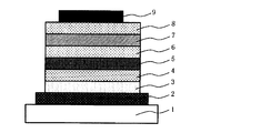
- FIG. 1 is a cross-sectional view schematically showing an example of the structure of the organic electroluminescent element of the present invention.
- the organic electroluminescent device shown in FIG. 1 is configured by laminating an anode, a hole injection layer, a hole transport layer, a light emitting layer, a hole blocking layer, an electron injection layer, and a cathode in this order on a substrate.
- the hole transport layer usually corresponds to the organic compound-containing layer of the present invention described above.
- Substrate serves as a support for the organic electroluminescence device, and quartz or glass plates, metal plates or metal foils, plastic films or sheets are used.
- a glass plate or a transparent synthetic resin plate such as polyester, polymethacrylate, polycarbonate, or polysulfone is preferable.
- a synthetic resin substrate it is necessary to pay attention to gas barrier properties. If the gas barrier property of the substrate is too small, the organic electroluminescent element may be deteriorated by the outside air that has passed through the substrate, which is not preferable. For this reason, a method of providing a gas barrier property by providing a dense silicon oxide film or the like on at least one surface of the synthetic resin substrate is also a preferable method.
- Anode plays a role of hole injection into a layer on the light emitting layer side (hole injection layer, light emitting layer, or the like) described later.
- This anode is usually a metal such as aluminum, gold, silver, nickel, palladium, or platinum, a metal oxide such as an oxide of indium and / or tin, a metal halide such as copper iodide, carbon black, or poly It is composed of conductive polymers such as (3-methylthiophene), polypyrrole and polyaniline.
- the anode is often formed by a sputtering method, a vacuum deposition method, or the like.
- anode can also be formed by coating.
- a thin film can be directly formed on a substrate by electrolytic polymerization, or an anode can be formed by applying a conductive polymer on a substrate (Applied Physics Letters, 1992, Vol. .60, pp. 2711).
- the anode can be formed by stacking different materials. The thickness of the anode varies depending on the required transparency.
- the visible light transmittance is usually 60% or more, preferably 80% or more.
- the thickness is usually 5 nm or more, preferably 10 nm or more, Usually, it is 1000 nm or less, preferably 500 nm or less.
- the anode may be the same as the substrate.
- the anode surface is treated with ultraviolet (UV) / ozone, oxygen plasma, or argon plasma for the purpose of removing impurities adhering to the anode and adjusting the ionization potential to improve hole injection. Is preferred.
- the hole injection layer is a layer that transports holes to a layer adjacent to the cathode side of the anode.
- the organic electroluminescent device of the present invention may have a configuration in which the hole injection layer is omitted.
- the hole injection layer preferably contains a hole transporting compound, and more preferably contains a hole transporting compound and an electron accepting compound.
- the hole injection layer preferably contains a cation radical compound, and particularly preferably contains a cation radical compound and a hole transporting compound.
- the hole injection layer may contain a binder resin and a coating property improving agent as necessary.
- the binder resin is preferably one that does not easily act as a charge trap.
- the hole injection layer can be formed by depositing only the electron-accepting compound on the anode by a wet film formation method, and directly applying and laminating the charge transport material composition thereon. In this case, a part of the charge transport material composition interacts with the electron accepting compound, whereby a layer having excellent hole injecting property is formed.
- the hole transporting compound As the hole transporting compound, a compound having an ionization potential of 4.5 eV to 6.0 eV is preferable. However, when used in the wet film forming method, it is preferable that the solubility in the solvent used in the wet film forming method is high.
- the hole transporting compound is preferably the charge transporting polymer of the present invention from the viewpoint of excellent film forming properties and high charge transporting ability. That is, it is preferable to form a layer using the composition for organic electroluminescent elements of the present invention.
- examples of the hole transporting compound include aromatic amine compounds, phthalocyanine derivatives, porphyrin derivatives, oligothiophene derivatives, polythiophene derivatives, and the like. It is done. Of these, aromatic amine compounds are preferred from the viewpoints of amorphousness and visible light transmittance.
- the type of the aromatic amine compound is not particularly limited, and may be a low molecular compound or a high molecular compound. From the viewpoint of the surface smoothing effect, a polymer having a weight average molecular weight of 1,000 or more and 1,000,000 or less. A compound (polymerizable hydrocarbon compound in which repeating units are continuous) is preferred.
- Preferable examples of the aromatic amine compound may also include an aromatic tertiary amine polymer compound having a repeating unit represented by the following formula (I).
- Ar b1 and Ar b2 are each independently a monovalent aromatic hydrocarbon group which may have a substituent, or an aromatic which may have a substituent.
- Ar b3 to Ar b5 each independently represents a divalent aromatic hydrocarbon group which may have a substituent or an aromatic group which may have a substituent.
- Z b represents a linking group selected from the following group of linking groups, and among Ar b1 to Ar b5 , two groups bonded to the same N atom are bonded to each other. A ring may be formed.
- Ar b6 to Ar b16 are each independently an aromatic hydrocarbon ring which may have a substituent, or an aromatic heterocyclic ring which may have a substituent.
- R b5 and R b6 each independently represents a hydrogen atom or an arbitrary substituent.
- any monovalent or divalent group derived from any aromatic hydrocarbon ring or aromatic heterocyclic ring is applicable. These groups may be the same or different from each other. Further, these groups may further have an arbitrary substituent.
- Specific examples of the aromatic tertiary amine polymer compound having a repeating unit represented by the general formula (I) include compounds described in International Publication No. 2005/089024 pamphlet.
- the hole transporting compound used as the material for the hole injection layer may contain any one of these compounds alone, or may contain two or more. When two or more hole transporting compounds are contained, the combination thereof is arbitrary, but one or more aromatic tertiary amine polymer compounds and one or two other hole transporting compounds are used. It is preferable to use the above together.
- the electron-accepting compound is the same as that described in the section ⁇ Composition for organic electroluminescence device>. The same applies to preferred specific examples.
- cation radical compound an ionic compound composed of a cation radical which is a chemical species obtained by removing one electron from a hole transporting compound and a counter anion is preferable.
- the cation radical is derived from a hole transporting polymer compound
- the cation radical has a structure in which one electron is removed from the repeating unit of the polymer compound.
- the cation radical is preferably a chemical species obtained by removing one electron from the compound described above as the hole transporting compound.
- a chemical species obtained by removing one electron from a compound preferable as a hole transporting compound is preferable in terms of amorphousness, visible light transmittance, heat resistance, solubility, and the like.
- the cation radical compound can be generated by mixing the hole transporting compound and the electron accepting compound. That is, by mixing the hole transporting compound and the electron accepting compound, electron transfer occurs from the hole transporting compound to the electron accepting compound, and the cation radical and the counter anion of the hole transporting compound
- a cation ion compound consisting of Cation radical compounds derived from polymer compounds such as PEDOT / PSS (Adv. Mater., 2000, 12, 481) and emeraldine hydrochloride (J. Phys. Chem., 1990, 94, 7716) It is also produced by oxidative polymerization (dehydrogenation polymerization).
- the oxidative polymerization referred to here is a method in which a monomer is chemically or electrochemically oxidized in an acidic solution using peroxodisulfate or the like.
- a monomer is oxidized to become a polymer, and an anion derived from an acidic solution is used as a counter anion. Generate.
- the hole injection layer can be formed by a wet film formation method or a dry film formation method such as a vacuum evaporation method. In view of excellent film formability, it is preferably formed by a wet film formation method.
- the thickness of the hole injection layer is usually 5 nm or more, preferably 10 nm or more, and usually 1000 nm or less, preferably 500 nm or less.
- the content of the electron-accepting compound in the hole-injecting layer with respect to the hole-transporting compound is usually 0.1 mol% or more, preferably 1 mol% or more. However, it is usually 100 mol% or less, preferably 40 mol% or less.
- hole injection layer As a material for the hole injection layer, other components may be further contained in addition to the above-described hole transporting compound and electron accepting compound as long as the effects of the present invention are not significantly impaired.
- other components include various light emitting materials, electron transporting compounds, binder resins, and coating property improving agents.
- 1 type may be used for another component and it may use 2 or more types together by arbitrary combinations and a ratio.
- At least one of the solvents of the composition for forming a hole injection layer used in the wet film formation method is preferably a compound that can dissolve the constituent material of the hole injection layer.
- the boiling point of this solvent is usually 110 ° C. or higher, preferably 140 ° C. or higher, particularly 200 ° C. or higher, usually 400 ° C. or lower, and preferably 300 ° C. or lower. If the boiling point of the solvent is too low, the drying speed is too high and the film quality may be deteriorated. Further, if the boiling point of the solvent is too high, it is necessary to increase the temperature of the drying process, which may adversely affect other layers and the substrate.
- ether solvents examples include aliphatic ethers such as ethylene glycol dimethyl ether, ethylene glycol diethyl ether, propylene glycol-1-monomethyl ether acetate (PGMEA); 1,2-dimethoxybenzene, 1,3-dimethoxybenzene, anisole , Aromatic ethers such as phenetole, 2-methoxytoluene, 3-methoxytoluene, 4-methoxytoluene, 2,3-dimethylanisole, 2,4-dimethylanisole, and the like.
- aliphatic ethers such as ethylene glycol dimethyl ether, ethylene glycol diethyl ether, propylene glycol-1-monomethyl ether acetate (PGMEA); 1,2-dimethoxybenzene, 1,3-dimethoxybenzene, anisole .
- Aromatic ethers such as phenetole, 2-methoxytoluene, 3-methoxytoluen
- ester solvent examples include aromatic esters such as phenyl acetate, phenyl propionate, methyl benzoate, ethyl benzoate, propyl benzoate, and n-butyl benzoate.
- aromatic hydrocarbon solvent examples include toluene, xylene, cyclohexylbenzene, 3- isopropylpropylphenyl, 1,2,3,4-tetramethylbenzene, 1,4-diisopropylbenzene, cyclohexylbenzene, and methylnaphthalene.
- amide solvent examples include N, N-dimethylformamide and N, N-dimethylacetamide.
- dimethyl sulfoxide and the like can also be used. These solvent may use only 1 type and may use 2 or more types by arbitrary combinations and a ratio.
- the composition After preparing the composition for forming a hole injection layer, the composition is applied onto a layer corresponding to the lower layer of the hole injection layer (usually an anode) by wet film formation and dried to form a hole injection layer.
- the temperature in the film forming step is preferably 10 ° C. or higher, and preferably 50 ° C. or lower in order to prevent film loss due to the formation of crystals in the composition.
- the relative humidity in a film-forming process is not limited unless the effect of this invention is impaired remarkably, it is 0.01 ppm or more normally and 80% or less normally.
- the film of the composition for forming a hole injection layer is usually dried by heating or the like.
- a heating step is usually performed.
- the heating means used in the heating step include a clean oven, a hot plate, an infrared ray, a halogen heater, and microwave irradiation. Among them, a clean oven and a hot plate are preferable in order to uniformly apply heat to the entire film.
- the heating temperature in the heating step is preferably heated at a temperature equal to or higher than the boiling point of the solvent used in the composition for forming a hole injection layer as long as the effects of the present invention are not significantly impaired.
- the heating temperature is preferably equal to or higher than the boiling point of the solvent of the composition for forming a hole injection layer.
- the heating time is not limited as long as sufficient crosslinking of the coating film does not occur, but it is preferably 10 seconds or longer and usually 180 minutes or shorter. If the heating time is too long, the components of the other layers tend to diffuse, and if it is too short, the hole injection layer tends to be inhomogeneous. Heating may be performed in two steps.
- the hole injection layer is formed by vacuum deposition
- one or more of the constituent materials of the hole injection layer (the aforementioned hole transporting compound, electron accepting compound, etc.) are placed in a vacuum container.
- crucibles in case of using two or more kinds of materials, put them in each crucible
- evacuate the inside of the vacuum vessel to about 10 -4 Pa with a suitable vacuum pump, and then heat the crucible (two or more kinds)
- heat each crucible heat each crucible and evaporate by controlling the amount of evaporation (when using two or more materials, evaporate by independently controlling the amount of evaporation) and place it facing the crucible.
- a hole injection layer is formed on the anode of the substrate.
- those hole mixture layers can also be formed by putting them in a crucible and heating and evaporating them.
- the degree of vacuum at the time of vapor deposition is not limited as long as the effects of the present invention are not significantly impaired, but usually 0.1 ⁇ 10 ⁇ 6 Torr (0.13 ⁇ 10 ⁇ 4 Pa) or more, usually 9.0 ⁇ 10 ⁇ 6 Torr. (12.0 ⁇ 10 ⁇ 4 Pa) or less.
- the deposition rate is not limited as long as the effect of the present invention is not significantly impaired, but is usually 0.1 ⁇ / second or more and usually 5.0 ⁇ / second or less.
- the film forming temperature at the time of vapor deposition is not limited as long as the effect of the present invention is not significantly impaired, but is preferably 10 ° C. or higher, preferably 50 ° C. or lower.
- the thickness of the hole injection layer is usually 5 nm or more, preferably 10 nm or more, and usually 1000 nm or less, preferably 500 nm or less.
- the hole transport layer can be formed on the hole injection layer when there is a hole injection layer and on the anode when there is no hole injection layer.
- the organic electroluminescent device of the present invention may have a configuration in which the hole transport layer is omitted.
- the material for forming the hole transport layer is preferably a material having a high hole transport capability and capable of efficiently transporting the injected holes. Therefore, it is preferable that the ionization potential is small, the transparency to visible light is high, the hole mobility is large, the stability is high, and impurities that become traps are not easily generated during manufacturing or use.
- the hole transporting compound the charge transporting polymer of the present invention is particularly preferable from the above point.
- a compound other than the charge transporting polymer of the present invention is used as the hole transporting compound, a material conventionally used as a constituent material of the hole transporting layer can be used. Examples of conventionally used materials include those exemplified as the hole transporting compound used in the above-described hole injection layer.
- aromatic amine compounds having a starburst structure such as aromatic diamines (Japanese Patent Laid-Open No. 5-234811), 4,4 ′, 4 ′′ -tris (1-naphthylphenylamino) triphenylamine (J. Lumin., 72-74, 985, 1997), an aromatic amine compound comprising a tetramer of triphenylamine (Chem.
- Spiro compounds such as tetrakis- (diphenylamino) -9,9′-spirobifluorene (Synth. Metals, 91, 209, 1997), 4,4′-N, N′-dicar Carbazole derivatives such as tetrazole biphenyl.
- polyvinyl carbazole polyvinyl triphenylamine (Japanese Unexamined Patent Publication No. 7-53953), polyarylene ether sulfone containing tetraphenylbenzidine (Polym. Adv. Tech., 7, 33, 1996). Etc.
- a composition for forming a hole transport layer is prepared in the same manner as in the formation of the hole injection layer, and then heated and dried after coating.
- the composition for forming a hole transport layer contains a solvent in addition to the above hole transport compound.
- the solvent used is the same as that used for the composition for forming a hole injection layer.
- the coating conditions, heating and drying conditions, and the like are the same as in the case of forming the hole injection layer.
- the film forming conditions are the same as in the case of forming the hole injection layer.
- the hole transport layer may contain various light emitting materials, electron transport compounds, binder resins, coatability improvers, and the like in addition to the hole transport compound.
- the hole transport layer may also be a layer formed by crosslinking a crosslinkable compound.
- the crosslinkable compound is a compound having a crosslinkable group, and forms a network polymer compound by crosslinking.
- Examples of such crosslinkable groups include cyclic ether groups such as oxetane groups and epoxy groups; groups containing unsaturated double bonds such as vinyl groups, trifluorovinyl groups, styryl groups, acrylic groups, methacryloyl groups, and cinnamoyl groups.
- the crosslinkable compound may be any of a monomer, an oligomer, and a polymer.
- the crosslinkable compound may have only 1 type, and may have 2 or more types by arbitrary combinations and ratios.
- a hole transporting compound having a crosslinkable group is preferably used.
- hole transporting compounds include nitrogen-containing aromatic compound derivatives such as pyridine derivatives, pyrazine derivatives, pyrimidine derivatives, triazine derivatives, quinoline derivatives, phenanthroline derivatives, carbazole derivatives, phthalocyanine derivatives, porphyrin derivatives; triphenylamine derivatives Silole derivatives; oligothiophene derivatives, condensed polycyclic aromatic derivatives, metal complexes and the like.
- nitrogen-containing aromatic derivatives such as pyridine derivatives, pyrazine derivatives, pyrimidine derivatives, triazine derivatives, quinoline derivatives, phenanthroline derivatives, carbazole derivatives; triphenylamine derivatives, silole derivatives, condensed polycyclic aromatic derivatives, metal complexes, etc.
- triphenylamine derivatives particularly preferred are triphenylamine derivatives.
- the composition for forming a hole transport layer may contain an additive for promoting a crosslinking reaction in addition to the crosslinking compound.
- additives that accelerate the crosslinking reaction include polymerization initiators and polymerization accelerators such as alkylphenone compounds, acylphosphine oxide compounds, metallocene compounds, oxime ester compounds, azo compounds, onium salts; condensed polycyclic hydrocarbons, And photosensitizers such as porphyrin compounds and diaryl ketone compounds.
- it may contain a coating property improving agent such as a leveling agent and an antifoaming agent; an electron accepting compound; a binder resin;
- the crosslinkable compound is usually 0.01% by weight or more, preferably 0.05% by weight or more, more preferably 0.1% by weight or more, usually 50% by weight or less, preferably 20%. It is contained by weight% or less, more preferably 10% by weight or less.
- the crosslinkable compound is formed by heating and / or irradiation with active energy such as light. It is crosslinked to form a network polymer compound.
- the thickness of the hole transport layer is usually 5 nm or more, preferably 10 nm or more, and usually 1000 nm or less, preferably 500 nm or less.
- the light emitting layer is formed on the hole transport layer when there is a hole transport layer, and on the hole injection layer when there is no hole transport layer without the hole transport layer. When there is no hole injection layer, it is formed on the anode.
- the light emitting layer may be a layer independent of the hole injection layer, the hole transport layer, and the hole blocking layer, the electron transport layer, etc., which will be described later, but does not form an independent light emitting layer.
- Other organic layers such as a transport layer and an electron transport layer may serve as the light emitting layer.
- the light-emitting layer is formed by directly injecting holes from an anode or through a hole injection layer or a hole transport layer between electrodes to which an electric field is applied, and directly from a cathode, or a cathode buffer layer or an electron transport layer. It is a layer that is excited by recombination with electrons injected through a hole blocking layer or the like and becomes a main light emitting source.
- the light emitting layer can be formed by any method as long as the effects of the present invention are not significantly impaired.
- the light emitting layer is formed on the anode by a wet film forming method or a vacuum deposition method.
- the wet film forming method is preferable.
- the wet film forming method and the vacuum deposition method can be performed using the same method as the hole injection layer.
- the light emitting layer contains at least a material having a light emitting property (light emitting material), and preferably a material having a hole transporting property (hole transporting material) or a material having an electron transporting property (electron). Transport material).
- the light emitting layer may contain other components without departing from the spirit of the present invention. As these materials, it is preferable to use low molecular weight materials from the viewpoint of forming a light emitting layer by a wet film forming method as described later.
- any known material can be applied as the light emitting material.
- a fluorescent material or a phosphorescent material may be used, but a phosphorescent material is preferable from the viewpoint of internal quantum efficiency.
- a phosphorescent material is preferable from the viewpoint of internal quantum efficiency.
- it is also important to reduce the symmetry and rigidity of the molecules of the luminescent material, or to introduce a lipophilic substituent such as an alkyl group.
- a fluorescent dye is not limited to the following illustrations.
- the fluorescent light-emitting material blue fluorescent dye
- examples of the fluorescent light-emitting material (blue fluorescent dye) that emits blue light include naphthalene, chrysene, perylene, pyrene, anthracene, coumarin, p-bis (2-phenylethenyl) benzene, and derivatives thereof.
- fluorescent dyes that give green light emission include quinacridone derivatives, coumarin derivatives, and aluminum complexes such as Al (C 9 H 6 NO) 3 .
- fluorescent light emitting material yellow fluorescent dye
- red fluorescent dyes examples include DCM (4- (dicyanomethyrene) -2-methyl-6- (p-dimethylaminostyryl) -4H-pyran) compounds, benzopyran derivatives, rhodamine derivatives, Examples thereof include benzothioxanthene derivatives and azabenzothioxanthene.
- phosphorescent materials include tris (2-phenylpyridine) iridium, tris (2-phenylpyridine) ruthenium, tris (2-phenylpyridine) palladium, bis (2-phenylpyridine) platinum, tris (2- Phenylpyridine) osmium, tris (2-phenylpyridine) rhenium, octaethylplatinum porphyrin, octaphenylplatinum porphyrin, octaethyl palladium porphyrin, octaphenyl palladium porphyrin, and the like.
- Polymeric light-emitting materials include poly (9,9-dioctylfluorene-2,7-diyl), poly [(9,9-dioctylfluorene-2,7-diyl) -co- (4,4′- (N- (4-sec-butylphenyl)) diphenylamine)], poly [(9,9-dioctylfluorene-2,7-diyl) -co- (1,4-benzo-2 ⁇ 2,1'-3 ⁇ -Triazole)], and polyphenylene vinylene materials such as poly [2-methoxy-5- (2-hexylhexyloxy) -1,4-phenylene vinylene].
- the charge transporting polymer of the present invention can also be used as a light emitting material.
- the molecular weight of the compound used as the light emitting material is arbitrary as long as the effect of the present invention is not significantly impaired, but is usually 10,000 or less, preferably 5000 or less, more preferably 4000 or less, still more preferably 3000 or less, and usually 100 or more, Preferably it is 200 or more, More preferably, it is 300 or more, More preferably, it is the range of 400 or more. If the molecular weight of the luminescent material is too small, the heat resistance will be significantly reduced, gas generation will be caused, the film quality will deteriorate when the film is formed, or the morphology of the organic electroluminescent element will change due to migration, etc. May come.
- the molecular weight of the luminescent material is too large, it tends to be difficult to purify the organic compound, or it may take time to dissolve in the solvent.
- only 1 type may be used for the luminescent material mentioned above, and 2 or more types may be used together by arbitrary combinations and a ratio.
- the ratio of the light emitting material in the light emitting layer is arbitrary as long as the effect of the present invention is not significantly impaired, but is preferably 0.05% by weight or more, and preferably 35% by weight or less. If the amount of the light emitting material is too small, uneven light emission may occur. If the amount is too large, the current efficiency may decrease.
- 2 or more types of luminescent material it is made for the total content of these to be contained in the said range.
- Examples of the low molecular weight hole transport material include various compounds exemplified as the hole transport material of the above-described hole transport layer, and 4,4′-bis [N- (1-naphthyl) -N—.
- Aromatic diamines including two or more tertiary amines, represented by phenylamino] biphenyl, wherein two or more condensed aromatic rings are substituted with nitrogen atoms (Japanese Patent Laid-Open No.
- low molecular weight electron transport materials examples include 2,5-bis (1-naphthyl) -1,3,4-oxadiazole (BND) and 2,5-bis (6 ′-(2 ′, 2 "-bipyridyl))-1,1-dimethyl-3,4-diphenylsilole (PyPySPyPy), bathophenanthroline (BPhen), 2,9-dimethyl-4,7-diphenyl-1,10-phenanthroline (BCP) , Bathocuproin), 2- (4-biphenylyl) -5- (p-tertiarybutylphenyl) -1,3,4-oxadiazole (tBu-PBD) and 4,4′-bis (9-carbazole) -Biphenyl (CBP), 9,10-di- (2-naphthyl) anthracene (ADN) and the like.
- BND 2,5-bis (1-naphthyl)
- hole transport materials and electron transport materials are preferably used as host materials in the light emitting layer.
- Specific examples of the host material include those described in Japanese Unexamined Patent Publication No. 2007-067383, Japanese Unexamined Patent Publication No. 2007-88433, Japanese Unexamined Patent Publication No. 2007-110093, and preferred examples thereof are also the same. It is.
- Examples of the method for forming the light emitting layer include a wet film forming method and a vacuum deposition method. As described above, a homogeneous and defect-free thin film can be easily obtained, and the time required for the formation can be shortened. Furthermore, a wet film-forming method is preferable because the effect of crosslinking the hole transport layer by the organic compound of the present invention can be enjoyed.
- a wet film-forming method is preferable because the effect of crosslinking the hole transport layer by the organic compound of the present invention can be enjoyed.
- a wet film-forming method prepare the coating solution by dissolving the above materials in an appropriate solvent, apply it to the hole transport layer after the above-mentioned formation, coat it, and dry it. Then, it is formed by removing the solvent.
- the formation method is the same as the formation method of the hole transport layer.
- the thickness of the light emitting layer is usually 3 nm or more, preferably 5 nm or more, and usually 300 nm or less, preferably 100
- Hole blocking layer A hole blocking layer 6 may be provided between the light emitting layer 5 and an electron injection layer 8 described later.
- the hole blocking layer 6 is a layer laminated on the light emitting layer 5 so as to be in contact with the interface of the light emitting layer 5 on the cathode 9 side.
- the hole blocking layer 6 has a role of blocking holes moving from the anode 2 from reaching the cathode 9 and a role of efficiently transporting electrons injected from the cathode 9 toward the light emitting layer 5.
- the physical properties required for the material constituting the hole blocking layer 6 include high electron mobility, low hole mobility, a large energy gap (difference between HOMO and LUMO), and excited triplet level (T1). Is high.
- Examples of the hole blocking layer material satisfying such conditions include bis (2-methyl-8-quinolinolato) (phenolato) aluminum, bis (2-methyl-8-quinolinolato) (triphenylsilanolato) aluminum, and the like.
- Triazole derivatives such as styryl compounds (Japanese Patent Laid-Open No. 11-242996), 3- (4-biphenylyl) -4-phenyl-5 (4-tert-butylphenyl) -1,2,4-triazole (Japan) Japanese Patent Laid-Open No. 7-41759), phenanthroline derivatives such as bathocuproine (Japanese Patent Laid-Open No. 10-79297) Broadcast), and the like. Further, a compound having at least one pyridine ring substituted at the 2,4,6-positions described in International Publication No. 2005-022962 is also preferable as a material for the hole blocking layer 6.
- the material of the hole-blocking layer 6 may use only 1 type, and may use 2 or more types together by arbitrary combinations and a ratio. There is no restriction
- FIG. Therefore, it can be formed by a wet film forming method, a vapor deposition method, or other methods.
- the thickness of the hole blocking layer 6 is arbitrary as long as the effect of the present invention is not significantly impaired, but is usually 0.3 nm or more, preferably 0.5 nm or more, and usually 100 nm or less, preferably 50 nm or less.
- Electron transport layer The electron transport layer is provided between the light emitting layer and the electron injection layer for the purpose of further improving the current efficiency of the device.
- the electron transport layer is formed of a compound that can efficiently transport electrons injected from the cathode between electrodes to which an electric field is applied in the direction of the light emitting layer.
- the electron transporting compound used in the electron transporting layer is a compound that has high electron injection efficiency from the cathode or the electron injection layer and has high electron mobility and can efficiently transport injected electrons. It is necessary.
- Materials satisfying such conditions include metal complexes such as aluminum complexes of 8-hydroxyquinoline (Japanese Unexamined Patent Publication No.
- metal complexes of 10-hydroxybenzo [h] quinoline, oxadiazole derivatives Distyrylbiphenyl derivatives, silole derivatives, 3- or 5-hydroxyflavone metal complexes, benzoxazole metal complexes, benzothiazole metal complexes, trisbenzimidazolylbenzene US Pat. No.
- the lower limit of the thickness of the electron transport layer is usually 1 nm, preferably about 5 nm, and the upper limit is usually about 300 nm, preferably about 100 nm.
- the electron transport layer is formed by laminating on the hole blocking layer by a wet film formation method or a vacuum deposition method in the same manner as described above. Usually, a vacuum deposition method is used.
- Electron injection layer plays a role of efficiently injecting electrons injected from the cathode into the electron transport layer or the light emitting layer.
- the material for forming the electron injection layer is preferably a metal having a low work function. Examples include alkali metals such as sodium and cesium, and alkaline earth metals such as barium and calcium.
- the film thickness is usually preferably from 0.1 nm to 5 nm.
- organic electron transport materials represented by metal complexes such as nitrogen-containing heterocyclic compounds such as bathophenanthroline and aluminum complexes of 8-hydroxyquinoline described later are doped with alkali metals such as sodium, potassium, cesium, lithium and rubidium.
- the film thickness in this case is usually in the range of 5 nm or more, preferably 10 nm or more, and usually 200 nm or less, preferably 100 nm or less.
- the electron injection layer is formed by laminating on the light emitting layer or the hole blocking layer thereon by a wet film formation method or a vacuum deposition method. Details of the wet film forming method are the same as those of the hole injection layer and the light emitting layer.
- the vacuum vapor deposition method the vapor deposition source is put into a crucible or a metal boat installed in the vacuum vessel, and the inside of the vacuum vessel is evacuated to about 10 ⁇ 4 Pa with an appropriate vacuum pump, and then the crucible or metal The boat is heated and evaporated to form an electron injection layer on the light emitting layer, hole blocking layer or electron transport layer on the substrate placed facing the crucible or metal boat.
- the alkali metal as the electron injection layer is deposited by using an alkali metal dispenser in which nichrome is filled with an alkali metal chromate and a reducing agent. By heating the dispenser in a vacuum container, the alkali metal chromate is reduced and the alkali metal is evaporated.
- the organic electron transport material and alkali metal are co-evaporated, the organic electron transport material is put in a crucible installed in a vacuum vessel, and the inside of the vacuum vessel is evacuated to about 10 ⁇ 4 Pa with an appropriate vacuum pump.
- Each crucible and dispenser are simultaneously heated and evaporated to form an electron injection layer on the substrate placed facing the crucible and dispenser. At this time, co-evaporation is uniformly performed in the film thickness direction of the electron injection layer, but there may be a concentration distribution in the film thickness direction.
- the cathode plays a role of injecting electrons into a layer on the light emitting layer side (such as an electron injection layer or a light emitting layer).
- a metal having a low work function is preferable, and tin, magnesium, indium, calcium, aluminum, A suitable metal such as silver or an alloy thereof is used.
- Specific examples include low work function alloy electrodes such as magnesium-silver alloy, magnesium-indium alloy, and aluminum-lithium alloy.
- the thickness of the cathode is usually the same as that of the anode.
- metals such as aluminum, silver, copper, nickel, chromium, gold, platinum are used.
- the organic electroluminescent element having the layer configuration shown in FIG. 1 has been described as an example.
- the organic electroluminescent element of the present invention may have another configuration without departing from the gist thereof.
- an arbitrary layer may be provided between the anode and the cathode in addition to the layers described above, and an arbitrary layer may be omitted.
- the charge transporting polymer of the present invention for the hole transport layer, all of the hole injection layer, the hole transport layer and the light emitting layer can be laminated by a wet film formation method. . This makes it possible to manufacture a large area display.
- a cathode, an electron injection layer, a light emitting layer, a hole injection layer, and an anode can be laminated in this order on a substrate, and at least one of them is transparent as described above. It is also possible to provide the organic electroluminescence device of the present invention between two high-height substrates. Further, a structure in which a plurality of layers shown in FIG. 1 are stacked (a structure in which a plurality of light emitting units are stacked) may be employed. In that case, for example, V 2 O 5 or the like is used as the charge generation layer (CGL) instead of the interfacial layer (between the light emitting units) (two layers when the anode is ITO and the cathode is Al).
- CGL charge generation layer
- the present invention can be applied to any of organic electroluminescent elements, a single element, an element having a structure arranged in an array, and a structure in which an anode and a cathode are arranged in an XY matrix.
- Organic EL display and the organic EL illumination of the present invention use the organic electroluminescent element of the present invention as described above.
- organic electroluminescent display of this invention and organic electroluminescent illumination, It can assemble in accordance with a conventional method using the organic electroluminescent element of this invention.
- the organic EL display and the organic EL display of the present invention can be obtained by the method described in “Organic EL display” (Ohm, August 20, 2004, published by Shizushi Tokito, Chiba Adachi, Hideyuki Murata). EL illumination can be formed.
- the target product 2 (2.31 g), tetrahydrofuran 15 mL, and ethanol 15 mL were added to a 100 mL eggplant flask and dissolved.
- 1.07 g of Raney nickel (R-200, manufactured by Nikko Rica Co., Ltd.) was added as a hydrogenation catalyst, and the mixture was replaced with hydrogen three times, followed by reaction at room temperature under hydrogen for 35 hours.
- the reaction solution was filtered through celite and concentrated with an evaporator to obtain 2.8 g of a crude product.
- Potassium fluoride (23.01 g) was charged into the reaction vessel, and heating and drying and nitrogen substitution were repeated under reduced pressure to create a nitrogen atmosphere in the system.
- 3-Nitrophenylboronic acid (6.68 g), 4-bromo-benzocyclobutene (7.32 g) and dehydrated tetrahydrofuran (50 ml) were charged and stirred.
- tris (dibenzylideneacetone) dipalladium chloroform complex (0.21 g)
- the inside of the system was sufficiently purged with nitrogen, and tri-t-butylphosphine (0.47 g) was added at room temperature. Thereafter, the mixture was stirred for 1 hour.
- the target product 8 (8.11 g), tetrahydrofuran 36 ml, ethanol 36 ml, 10% Pd / C (1.15 g) were charged, and the mixture was heated and stirred at 70 ° C. Hydrazine monohydrate (10.81 g) was slowly added dropwise thereto. After reacting for 2 hours, the mixture was allowed to cool, the reaction mixture was filtered through celite, and the filtrate was concentrated. Ethyl acetate was added to the filtrate, washed with water, and the organic layer was concentrated. The resulting crude product was purified by column chromatography (hexane / ethyl acetate) to give the intended product 9 (4.90 g). (Synthesis Example 10)
- the target product 10 (2.89 g), 2,7-dibromofluorene (1.17 g) and dimethyl sulfoxide (30 ml) were placed in a 100 ml four-necked flask and stirred, and the temperature was raised to 60 ° C. Crushed sodium hydroxide (0.72 g) was dissolved in 5 ml of water, dropped into this solution, and reacted for 3 hours. 50 ml of hexane was added to the reaction solution and washed with 30 ml of water. The oil layer was concentrated and subjected to column purification.
- the target product 12 (2.70 g), 1-bromohexane (1.31 g), tetra-n-butylammonium bromide (0.34 g) and dimethyl sulfoxide (30 ml) were added to the reactor, and the temperature was raised to 60 ° C. It returned to room temperature. An aqueous solution (1.2 ml) of sodium hydroxide (0.64 g) was added dropwise. After stirring for 1.5 hours, water (60 ml) and ethyl acetate (100 ml) were added to the reaction solution, the organic layer was concentrated, and the resulting oily component was purified by silica gel chromatography (hexane / methylene chloride). The target product 13 (1.80 g) was obtained. (Synthesis Example 14)
- the desired product 14 (3.64 g), 4-bromoiodobenzene (3.97 g), toluene (60 ml), ethanol (30 ml), 2M aqueous sodium carbonate solution (30 ml) were added to the reactor, and the temperature was raised to 50 ° C. After warming, tetrakis (triphenylphosphine) palladium (0.40 g) was added. The temperature was raised to 80 ° C. and stirred for 8 hours.
- Target 5 (1.086 g, 3.1075 mmol), Target 3 (0.184 g, 0.5984 mmol), aniline (0.197 g, 2.1185 mmol), 4,4′-dibromobiphenyl (0.891 g, 2 .8551 mmol), sodium tert-butoxy (1.76 g, 18.27 mmol) and toluene (23 ml) were charged, and the system was sufficiently purged with nitrogen and heated to 60 ° C. (solution A).
- Tri-t-butylphosphine (0.092 g, 0.457 mmol) was added to a toluene 2 ml solution of tris (dibenzylideneacetone) dipalladium chloroform complex (0.059 g, 0.057 mmol) and heated to 60 ° C. ( Solution B). In a nitrogen stream, solution B was added to solution A, and the mixture was heated to reflux for 1.5 hours. After confirming disappearance of the target compound 5, target compound 3, aniline, and 4,4'-dibromobiphenyl, 4,4'-dibromobiphenyl (0.8375 g, 2.684 mmol) was further added.
- Target 3 (0.1087 g), Target 5 (1.185 g), Target 7 (0.069 g), 9,10-bis (4-bromophenyl) anthracene (1.000 g), and sodium tert-butoxy (1.26 g, toluene (10 ml) was charged, the inside of the system was sufficiently purged with nitrogen, and the mixture was heated to 50 ° C.
- solution E Tris (dibenzylideneacetone) dipalladium chloroform complex (0.042 g) in toluene Tri-t-butylphosphine (0.066 g) was added to a 2 ml solution and heated to 50 ° C.
- Solution F Solution F was added to Solution E in a nitrogen stream and the mixture was heated to 90 ° C. for 1.5 hours. Subsequently, 9,10-bis (4-bromophenyl) anthracene (0.940 g) was further added, and the mixture was heated to reflux for 1 hour, and then the reaction mixture was allowed to cool, and the reaction mixture was stirred with ethanol. The crude polymer 2 was crystallized.
- the obtained crude polymer 2 was dissolved in 150 ml of toluene, bromobenzene (0.52 g) and tert-butoxy sodium (0.63 g) were charged, the inside of the system was sufficiently purged with nitrogen, and the mixture was heated to 50 ° C. ( Solution G).
- Tri-t-butylphosphine (0.033 g) was added to a 2 ml toluene solution of tris (dibenzylideneacetone) dipalladium chloroform complex (0.021 g) and heated to 50 ° C. (solution H). In a nitrogen stream, the solution H was added to the solution G, and the mixture was heated to reflux for 3 hours.
- Diphenylbenzidine (2.07 g, 6.2 mmol), target compound 11 (0.43 g, 0.6 mmol), 9.9′-dihexyl-2,7-dibromofluorene (2.63 g, 5.3 mmol), and tert -Butoxy sodium (2.22 g, 23.0 mmol) and toluene (20 ml) were charged, the inside of the system was sufficiently purged with nitrogen, and the mixture was heated to 50 ° C. (solution I).
- Tri-t-butylphosphine (0.10 g, 0.049 mmol) was added to a 15 ml toluene solution of tris (dibenzylideneacetone) dipalladium chloroform complex (0.07 g, 0.0068 mmol) and heated to 50 ° C. ( Solution J). In a nitrogen stream, solution J was added to solution I, and the mixture was heated to reflux for 1 hour. After confirming the disappearance of diphenylbenzidine, target 11, 9.9′-dihexyl-2,7-dibromofluorene, 9.9′-dihexyl-2,7-dibromofluorene (1.91 g, 6.1 mmol) was confirmed. Was added.
- the obtained crude polymer 3 was dissolved in 100 ml of toluene, bromobenzene (0.97 g, 6.2 mmol) and sodium tert-butoxy (0.710 g, 7 mmol) were charged, and the inside of the system was sufficiently purged with nitrogen. Warmed to 0 ° C. (Solution K). Tri-t-butylphosphine (0.012 g, 0.0062 mmol) was added to a 10 ml toluene solution of tris (dibenzylideneacetone) dipalladium chloroform complex (0.051 g, 0.0049 mmol) and heated to 50 ° C. ( Solution L).
- the solution L was added to the solution K, and the mixture was heated to reflux for 2 hours.
- N, N-diphenylamine (1.041 g, 6.15 mmol) was added to the reaction solution, and the mixture was further heated to reflux for 2 hours.
- the reaction solution was allowed to cool and added dropwise to methanol to obtain an end-capped crude polymer 3.
- This end-capped crude polymer 3 was dissolved in toluene, reprecipitated in acetone, and the precipitated polymer was separated by filtration.
- the obtained polymer was dissolved in toluene, washed with dilute hydrochloric acid, and reprecipitated with ammonia-containing ethanol.
- target 15 (0.659 g), target 16 (1.22 g), aniline (0.516 g), tert-butoxy sodium (1.70 g), and toluene (20 ml) were added to the reactor. Warmed to 50 ° C. (Solution A). Tri-t-butylphosphine (0.089 g) was added to a 1 ml toluene solution of tris (dibenzylideneacetone) dipalladium chloroform complex (0.0057 g) and heated to 50 ° C. (solution B). In a nitrogen stream, solution B was added to solution A and heated to reflux for 1 hour. After confirming disappearance of the raw material, the target product 16 (1.78 g) was added. The reaction was heated to reflux for 40 minutes. The reaction solution was allowed to cool, and the reaction solution was dropped into 200 ml of ethanol to crystallize the crude polymer 4.
- This end-capped crude polymer 4 was dissolved in toluene, washed with dilute hydrochloric acid, and reprecipitated with ammonia-containing ethanol. Then, it melt
- the target product 13 (1.50 g), 2,7-dibromo-9,9-dihexylfluorene (0.683 g), aniline (0.728 g), tert-butoxy sodium (2.41 g) were placed in a reactor. And toluene (15 ml) were added and warmed to 50 ° C. (solution A). Tri-t-butylphosphine (0.126 g) was added to a 1 ml toluene solution of tris (dibenzylideneacetone) dipalladium chloroform complex (0.080 g) and heated to 50 ° C. (solution B). In a nitrogen stream, solution B was added to solution A and heated to reflux for 1 hour.
- Tri-t-butylphosphine (0.16 g, 0.8 mmol) was added to a 6 ml toluene solution of tris (dibenzylideneacetone) dipalladium chloroform complex (0.10 g, 0.1 mmol) and heated to 50 ° C. (solution N ).
- Solution N was added to solution M in a nitrogen stream, and the mixture was heated to reflux for 1 hour. After confirming the disappearance of aniline, target product 9, target product 5, 4,4′-dibromobiphenyl, 4,4′-dibromobiphenyl (1.41 g, 4.5 mmol) was further added.
- the obtained crude polymer 6 was dissolved in 70 ml of toluene, bromobenzene (0.30 g, 1.9 mmol) and tert-butoxy sodium (1.48 g, 15.3 mmol) were charged, and the inside of the system was sufficiently purged with nitrogen. Warmed to 0 ° C. (Solution O). Tri-t-butylphosphine (0.08 g, 0.4 mmol) was added to a 4 ml toluene solution of tris (dibenzylideneacetone) dipalladium chloroform complex (0.05 g, 0.05 mmol) and heated to 50 ° C. (solution P ).
- the solution P was added to the solution O, and the mixture was heated to reflux for 2 hours.
- N, N-diphenylamine (1.63 g, 9.6 mmol) was added to the reaction solution, and the mixture was further heated to reflux for 4 hours.
- the reaction solution was allowed to cool and dropped into an aqueous ethanol solution (ethanol 150 ml + water 25 ml) to obtain end-capped crude polymer 6.
- This end-capped crude polymer 6 was dissolved in toluene, reprecipitated in acetone, and the precipitated polymer was separated by filtration.
- the obtained polymer was dissolved in toluene, washed with dilute hydrochloric acid, and reprecipitated with ammonia-containing ethanol.
- Target 9 (0.1702 g), Target 5 (1.485 g), 9,10-bis (4-bromophenyl) anthracene (1.250 g), tert-butoxy sodium (1.58 g), toluene (12 ml) ),
- the inside of the system was sufficiently substituted with nitrogen, and heated to 50 ° C. (solution Q).
- Tri-t-butylphosphine (0.083 g) was added to a 3 ml toluene solution of tris (dibenzylideneacetone) dipalladium chloroform complex (0.053 g) and heated to 50 ° C. (solution R). In a nitrogen stream, the solution R was added to the solution Q, and the reaction was performed by heating to 90 ° C.
- Tri-t-butylphosphine (0.030 g) was added to a 3 ml toluene solution of tris (dibenzylideneacetone) dipalladium chloroform complex (0.019 g) and heated to 50 ° C. (solution T).
- solution T was added to the solution S in a nitrogen stream, and the mixture was heated to reflux for 2 hours.
- N, N-diphenylamine (0.30 g) was added, and the solution T prepared again was added, and the mixture was further heated to reflux for 5 hours.
- the reaction solution was allowed to cool and dropped into ethanol to obtain an end-capped crude polymer 7.
- ⁇ Composition for organic electroluminescence device Solvent Toluene Solid content concentration 1.0% by weight
- ⁇ Composition for organic electroluminescence device Solvent Toluene Solid content concentration 1.0% by weight
- the film thus obtained was measured for a fluorescence spectrum at an excitation light wavelength of 375 nm using a spectrophotometer F-4500 (manufactured by Hitachi, Ltd.). As a result, the wavelength at which the fluorescence intensity was maximum was 462 nm. It was.
- Table 1 shows the fluorescence wavelengths of the films prepared in Reference Example 1 and Comparative Reference Example 1.
- the film formed using the charge transporting polymer of the present invention has a fluorescence wavelength on the short wavelength side. That is, it can be seen that the film formed using the charge transporting polymer of the present invention has little uneven aggregation.
- the organic electroluminescent element shown in FIG. 1 was produced.
- An anode was formed by patterning into a stripe having a width of 2 mm.
- the patterned ITO substrate is cleaned in the order of ultrasonic cleaning with an aqueous surfactant solution, water cleaning with ultrapure water, ultrasonic cleaning with ultrapure water, and water cleaning with ultrapure water, followed by drying with compressed air, and finally UV irradiation. Ozone cleaning was performed.
- a hole-transporting polymer material having a repeating structure represented by the following structural formula (P1) (weight average molecular weight: 26500, number-average molecular weight: 12000), 4-isopropyl-4 ′-represented by the structural formula (A1)
- P1 weight average molecular weight: 26500, number-average molecular weight: 12000
- a composition for a hole injection layer containing methyldiphenyliodonium tetrakis (pentafluorophenyl) borate and ethyl benzoate was prepared. This composition was applied onto the anode by spin coating under the following conditions to obtain a hole injection layer having a thickness of 30 nm.
- a composition for an organic electroluminescence device containing the charge transporting polymer (H1) of the present invention (target polymer 1 synthesized in Polymer Synthesis Example 1) represented by the following structural formula was prepared, and the conditions were as follows.
- a hole transport layer having a thickness of 20 nm was formed by coating by spin coating and crosslinking by heating.
- ⁇ Composition for organic electroluminescence device Solvent Toluene Composition concentration 0.4% by weight
- ⁇ Hole transport layer deposition conditions Spinner speed 1500rpm Spinner rotation time 30 seconds Spin coat atmosphere In nitrogen Heating conditions In nitrogen, 230 ° C, 1 hour
- the following organic electroluminescent element composition is prepared using the organic compounds (C1) and (D1) shown below, and is formed on the hole transporting layer under the conditions shown below.
- a light emitting layer was obtained with a film thickness of 40 nm by spin coating.
- the substrate on which the light emitting layer has been formed is transferred into a vacuum vapor deposition apparatus connected to a nitrogen glove box, exhausted until the degree of vacuum in the apparatus becomes 1.7 ⁇ 10 ⁇ 4 Pa or less, and then BAlq (C2) was laminated by a vacuum deposition method to obtain a hole blocking layer.
- the deposition rate was controlled in the range of 0.5 to 1.1 liters / second, and a hole blocking layer having a thickness of 10 nm was formed by laminating on the light emitting layer.
- the degree of vacuum during deposition was 2.6 to 3.9 ⁇ 10 ⁇ 5 Pa.
- Alq3 (C3) was heated and vapor-deposited, and the electron carrying layer was formed into a film.
- the degree of vacuum during deposition is 2.8 to 3.7 ⁇ 10 ⁇ 5 Pa, the deposition rate is controlled in the range of 0.7 to 1.2 liters / second, and a 30 nm thick film is formed on the hole blocking layer.
- the electron transport layer was formed by laminating.
- the element that has been vapor-deposited up to the electron transport layer is transported in a vacuum to a chamber connected to the chamber in which the hole-blocking layer and the electron transport layer are vapor-deposited, and a 2 mm wide stripe as a mask for cathode vapor deposition.
- a thin shadow mask was adhered to the element so as to be orthogonal to the ITO stripe of the anode.
- the electron injection layer first, lithium fluoride (LiF) was controlled using a molybdenum boat at a deposition rate of 0.09 to 0.14 liters / second and a degree of vacuum of 2.7 to 5.4 ⁇ 10 ⁇ 5 Pa. A film having a thickness of 0.5 nm was formed on the electron transport layer.
- aluminum as a cathode is similarly heated by a molybdenum boat and controlled at a deposition rate of 0.5 to 1.3 liters / second and a degree of vacuum of 2.1 to 5.4 ⁇ 10 ⁇ 5 Pa. An aluminum layer was formed. The substrate temperature during the above two-layer deposition was kept at room temperature.
- a sealing process was performed by the method described below.
- a photocurable resin 30Y-437 manufactured by ThreeBond
- a moisture getter sheet manufactured by Dynic
- finished cathode formation was bonded together so that the vapor-deposited surface might oppose a desiccant sheet.
- Example 1 the organic electroluminescent element shown in FIG. 1 was produced in the same manner as Example 1 except that the hole transport layer was formed as follows.
- a composition for an organic electroluminescence device containing a compound (H2) represented by the following structural formula (Comparative Polymer 1 synthesized in Synthesis Example 1 for Comparative Polymer) was prepared, applied by spin coating under the following conditions, and heated.
- the hole transport layer having a film thickness of 20 nm was formed by cross-linking.
- ⁇ Composition for organic electroluminescence device Solvent Toluene Composition concentration 0.4% by weight
- ⁇ Hole transport layer deposition conditions Spinner speed 1500rpm Spinner rotation time 30 seconds Spin coat atmosphere In nitrogen Heating conditions In nitrogen, 230 ° C, 1 hour
- the light emission characteristics of the organic electroluminescent element having a light emitting area portion of 2 mm ⁇ 2 mm obtained in this way are as follows.
- Luminance at 10 mA / cm 2 energization 4663 cd / m 2 Voltage at 10 mA / cm 2 energization: 7.5V Power efficiency at 100 cd / m 2 : 0.9 lm / W
- the maximum wavelength of the emission spectrum of the device was 465 nm, and it was identified as that from the compound (D1).
- Table 2 shows that the organic electroluminescence device having a layer formed by crosslinking the charge transporting polymer of the present invention has a low driving voltage, high power efficiency, and a long driving life.
- Example 2 The organic electroluminescent element shown in FIG. 1 was produced in the same manner as in Example 1 except that the hole transport layer and the light emitting layer were formed as follows in Example 1.
- a composition for an organic electroluminescent device containing the charge transporting polymer (H3) according to the present invention (target polymer 2 synthesized in Polymer Synthesis Example 2) represented by the following structural formula was prepared and spin-coated under the following conditions: And a hole transport layer having a thickness of 20 nm was formed by crosslinking by heating.
- ⁇ Composition for organic electroluminescence device Solvent Toluene Composition concentration 0.4% by weight
- ⁇ Hole transport layer deposition conditions Spinner speed 1500rpm Spinner rotation time 30 seconds Spin coat atmosphere In nitrogen Heating conditions In nitrogen, 230 ° C, 1 hour
- the organic compound (C4) and (D1) shown below are used to prepare the organic electroluminescent element composition shown below, and on the hole transport layer under the conditions shown below.
- a light emitting layer was obtained with a film thickness of 40 nm by spin coating.
- Luminance at 10 mA / cm 2 energization 9477 cd / m 2 Voltage at 10 mA / cm 2 energization: 7.5V Power efficiency at 100 cd / m 2 : 2.0 lm / W
- the maximum wavelength of the emission spectrum of the device was 465 nm, and it was identified as that from the compound (D1).
- Example 2 the organic electroluminescent element shown in FIG. 1 was produced in the same manner as in Example 2 except that the hole transport layer was formed as follows.
- a composition for an organic electroluminescence device containing a compound (H4) represented by the following structural formula (Comparative Polymer 2 synthesized in Synthesis Example 2 for Comparative Polymer) was prepared, applied by spin coating under the following conditions, and heated.
- the hole transport layer having a film thickness of 20 nm was formed by cross-linking.
- ⁇ Composition for organic electroluminescence device Solvent Toluene Composition concentration 0.4% by weight
- ⁇ Hole transport layer deposition conditions Spinner speed 1500rpm Spinner rotation time 30 seconds Spin coat atmosphere In nitrogen Heating conditions In nitrogen, 230 ° C, 1 hour
- the light emission characteristics of the organic electroluminescent element having a light emitting area portion of 2 mm ⁇ 2 mm obtained in this way are as follows.
- Luminance at 10 mA / cm 2 energization 8670 cd / m 2 10mA / cm 2 current at the time of the voltage: 7.4V Power efficiency at 100 cd / m 2 : 1.8 lm / W
- the maximum wavelength of the emission spectrum of the device was 464 nm, which was identified as that from the compound (D1).
- Table 3 shows that the organic electroluminescent device having a layer formed by crosslinking the charge transporting polymer of the present invention has high power efficiency and a long driving life.
- Example 3 the organic electroluminescent element shown in FIG. 1 was produced in the same manner as in Example 2 except that the hole transport layer was formed as follows.
- a composition for an organic electroluminescent device containing the charge transporting polymer (H5) according to the present invention (target polymer 4 synthesized in Polymer Synthesis Example 4) represented by the following structural formula was prepared, and spin was performed under the following conditions.
- a hole transport layer having a thickness of 20 nm was formed by coating by coating and crosslinking by heating.
- ⁇ Composition for organic electroluminescence device Solvent Toluene Composition concentration 0.4% by weight
- ⁇ Hole transport layer deposition conditions Spinner speed 1500rpm Spinner rotation time 30 seconds Spin coating atmosphere Heating condition in nitrogen Heating condition in nitrogen, 230 ° C., 1 hour
- the organic electroluminescence device having a light emitting area portion of 2 mm ⁇ 2 mm obtained in this way has the following emission characteristics. is there.
- Example 3 The organic electroluminescent element shown in FIG. 1 was produced in the same manner as in Example 3 except that the hole transport layer was formed as follows in Example 3.
- the hole transport layer having a thickness of 20 nm was formed by coating by spin coating and crosslinking by heating.
- ⁇ Composition for organic electroluminescence device Solvent Toluene Composition concentration 0.4% by weight
- ⁇ Hole transport layer deposition conditions Spinner speed 1500rpm Spinner rotation time 30 seconds Spin coating atmosphere Heating condition in nitrogen Heating condition in nitrogen, 230 ° C., 1 hour
- the organic electroluminescence device having a light emitting area portion of 2 mm ⁇ 2 mm obtained in this way has the following emission characteristics. is there.
- Table 4 shows that the organic electroluminescent device having a layer formed by crosslinking the charge transporting polymer of the present invention has a low driving voltage, high current efficiency, and a long life.
- Example 4 the organic electroluminescent element shown in FIG. 1 was produced in the same manner as in Example 2 except that the hole transport layer was formed as follows.
- a composition for an organic electroluminescent device containing the charge transporting polymer (H7) according to the present invention (target polymer 3 synthesized in Polymer Synthesis Example 3) represented by the following structural formula was prepared, and spin was performed under the following conditions.
- a hole transport layer having a thickness of 20 nm was formed by coating by coating and crosslinking by heating.
- ⁇ Composition for organic electroluminescence device Solvent Toluene Composition concentration 0.4% by weight
- ⁇ Hole transport layer deposition conditions Spinner speed 1500rpm Spinner rotation time 30 seconds Spin coating atmosphere Heating condition in nitrogen Heating condition in nitrogen, 230 ° C., 1 hour
- the organic electroluminescence device having a light emitting area portion of 2 mm ⁇ 2 mm obtained in this way has the following emission characteristics. is there. Voltage at 100 cd / m 2 : 5.6V Current efficiency at 100 cd / m 2 : 2.6 cd / A
- the maximum wavelength of the emission spectrum of the device was 465 nm, and it was identified as that from the compound (D1).
- Example 4 the organic electroluminescent element shown in FIG. 1 was produced in the same manner as in Example 4 except that the hole transport layer was formed as follows.
- a composition for an organic electroluminescent device containing a charge transporting polymer (H8) (Mw: 55000, Mn: 28900, Mw / Mn: 1.9) represented by the following structural formula was prepared, and spin was performed under the following conditions.
- a hole transport layer having a thickness of 20 nm was formed by coating by coating and crosslinking by heating.
- ⁇ Composition for organic electroluminescence device Solvent Toluene Composition concentration 0.4% by weight
- ⁇ Hole transport layer deposition conditions Spinner speed 1500rpm Spinner rotation time 30 seconds Spin coating atmosphere Heating condition in nitrogen Heating condition in nitrogen, 230 ° C., 1 hour
- the organic electroluminescence device having a light emitting area portion of 2 mm ⁇ 2 mm obtained in this way has the following emission characteristics. is there. Voltage at 100 cd / m 2 : 5.8V Current efficiency at 100 cd / m 2 : 2.2 cd / A
- the maximum wavelength of the emission spectrum of the device was 467 nm, which was identified as from the compound (D1).
- Table 5 shows that the organic electroluminescence device having a layer formed by crosslinking the charge transporting polymer of the present invention has a low driving voltage, high current efficiency, and a long driving life.
- Example 5 A measuring element having a single-layer structure was produced in the manner described below.
- ITO indium tin oxide
- the patterned ITO substrate is cleaned in the order of ultrasonic cleaning with an aqueous surfactant solution, water cleaning with ultrapure water, ultrasonic cleaning with ultrapure water, and water cleaning with ultrapure water, followed by drying with compressed air, and finally UV irradiation. Ozone cleaning was performed.
- the spinner rotation speed was 1500 rpm, and the spinner time was 30 seconds. After spin coating, it was heated at 230 ° C. for 1 hour in an oven at atmospheric pressure. In this way, a sample layer (corresponding to a hole injection layer of an organic electroluminescence device) 10 was formed.
- a stripe shadow mask having a width of 2 mm as a mask for cathode vapor deposition was brought into close contact with the element so as to be orthogonal to the ITO stripe of the anode 2.
- the apparatus was evacuated with a cryopump until the degree of vacuum in the apparatus was 3 ⁇ 10 ⁇ 4 Pa or less.
- Aluminum was heated as a cathode 9 by a molybdenum boat, and an aluminum layer having a thickness of 80 nm was formed by controlling the deposition rate at 0.5 to 5 liters / second and the degree of vacuum at 2 to 3 ⁇ 10 ⁇ 4 Pa.
- the substrate temperature during the deposition of the cathode 9 was kept at room temperature.
- a measuring element having an element area of 2 mm ⁇ 2 mm was obtained.
- the obtained measurement element was connected to a 2400 type source meter (manufactured by Keithley), and voltage was sequentially applied to read the current value.
- the voltage at a current density of 100 mA / cm 2 showed a low value of 5.6V.
- the obtained measurement element was connected to a 2400 type source meter (manufactured by Keithley), and voltage was sequentially applied to read the current value. As a result, the voltage at a current density of 100 mA / cm 2 was 8.3V. It can be seen that the organic electroluminescent device containing an electron accepting compound in the layer formed by crosslinking the charge transporting polymer of the present invention has a low driving voltage.
- the charge transporting polymer of the present invention has a hole injection material, a hole transporting material, an excellent electrochemical stability, film forming property, charge transporting ability, light emitting property, and heat resistance according to the layer structure of the device. It can also be applied as a light emitting material, a host material, an electron injection material, an electron transport material and the like.
- the organic electroluminescent device having a layer (crosslinked layer) obtained by crosslinking the charge transporting polymer of the present invention is a flat panel display (for example, for OA computers or wall-mounted televisions), an in-vehicle display device, a mobile phone display or surface light emission.
- the charge transporting polymer of the present invention has essentially excellent redox stability, it is useful not only for organic electroluminescent devices but also for organic devices such as electrophotographic photoreceptors and organic solar cells. .
Abstract
Description
真空蒸着法は積層化が容易であるため、陽極及び/又は陰極からの電荷注入の改善、励起子の発光層封じ込めが容易であるという利点を有する。湿式成膜法は真空プロセスが要らず、大面積化が容易で、1つの層(組成物)に様々な機能をもった複数の材料を混合して入れることが容易である等の利点がある。
しかしながら、湿式成膜法は積層化が困難であるため、真空蒸着法による素子に比べて駆動安定性に劣り、一部を除いて実用レベルに至っていないのが現状である。特に、湿式成膜法での積層化は、有機溶剤と水系溶剤を使用するなどして二層の積層は可能であるが、三層以上の積層化は困難であった。
このような積層化における問題点を解決するために、特許文献1では、下記のように架橋性基としてオキセタン基を有するポリマーが提案され、このポリマーを塗布し、オキセタン基を反応させた層が開示されている。この層は、有機溶剤に不溶化しているため、この層上に他の層を積層することが可能である旨開示されている。しかしながら、この方法により得られる素子は、定電流通電時の駆動電圧が上昇したり、通電時の輝度安定性が低下したりして、駆動寿命が短いという課題があった。さらに、この方法では、平坦な層が形成されず、得られる素子の発光面が均一でないとの課題もあった。


また、ポリマー主鎖の凝集が、成膜性や膜の平坦性に影響していることを見出した。
そこで、これらの知見をもとに、分子設計を試みたところ、側鎖に下記式(1)で表される基を有する電荷輸送性ポリマーであれば、上記影響がなく、電力効率が高く、駆動電圧が低く、また駆動寿命が長い素子が得られることを見出して、本発明に到達した。
即ち、本発明は、側鎖に、下記式(1)で表される基を有することを特徴とする、電荷輸送性ポリマー及びこれを用いてなる有機電界発光素子用組成物、有機電界発光素子、並びに有機ELディスプレイ及び有機EL照明に存する。

[1]
側鎖として、下記式(1)で表される基を有することを特徴とする、電荷輸送性ポリマー。

[2]
前記式(1)で表される基が、下記式(2)で表される基であることを特徴とする、上記[1]に記載の電荷輸送性ポリマー。

R1~R3は、各々独立して、水素原子又は置換基を有していてもよいアルキル基を表す。
また、n個のQは、同じでもよく、また異なっていてもよい。
また、式(2)中のベンゾシクロブテン環は、2価の基Q以外に、置換基を有していてもよい。)
[3]
前記式(2)で表される基が、下記式(3)で表される基であることを特徴とする、上記[2]に記載の電荷輸送性ポリマー。

また、q個のR1及びR2は、各々独立に、同じでもよく、また異なっていてもよい。
また、式(3)中のベンゾシクロブテン環は、-(CR1R2)q-基以外に、置換基を有していてもよい。)
[4]
部分構造としてトリアリールアミン構造由来の1価以上の基を含むことを特徴とする、上記[1]~[3]のいずれかに記載の電荷輸送性ポリマー。
[5]
部分構造としてフルオレン環由来の1価以上の基を含むことを特徴とする、上記[1]~[4]のいずれかに記載の電荷輸送性ポリマー。
[6]
重量平均分子量(Mw)が20,000以上であり、分散度(Mw/Mn)が2.5以下であることを特徴とする、上記[1]~[5]のいずれかに記載の電荷輸送性ポリマー。
(但し、Mnは数平均分子量を表す。)
[7]
下記式(4)で表される繰り返し単位を含むことを特徴とする、上記[1]~[6]のいずれかに記載の電荷輸送性ポリマー。

Ar11、及びAr12は、各々独立して、直接結合、置換基を有していてもよい芳香族炭化水素基又は置換基を有していてもよい芳香族複素環基を表し、
Ar13~Ar15は、各々独立に、置換基を有していてもよい芳香族炭化水素基又は置換基を有していてもよい芳香族複素環基を表す。
但し、Ar11及びAr12が同時に、直接結合であることはない。)
[8]
前記式(1)で表される基を、分子量1,000あたり0.01個以上、3個以下有することを特徴とする、上記[1]~[7]のいずれかに記載の電荷輸送性ポリマー。
(但し、分子量は、該電荷輸送性ポリマーからその末端基を除いて、仕込みモノマーのモル比と構造式から算出される値である。)
[9]
下記式(5)で表される基を有することを特徴とする、上記[1]~[8]のいずれかに記載の電荷輸送性ポリマー。

[10]
上記[1]~[9]のいずれかに記載の電荷輸送性ポリマー及び溶剤を含有することを特徴とする、有機電界発光素子用組成物。
[11]
さらに、電子受容性化合物を含有することを特徴とする、上記[10]に記載の有機電界発光素子用組成物。
[12]
基板上に、陽極、陰極、及び該陽極と該陰極の間に有機層を有する有機電界発光素子において、該有機層が、上記[10]又は[11]に記載の有機電界発光素子用組成物を用いて塗布後、前記電荷輸送性ポリマーを架橋して形成される層を含むことを特徴とする、有機電界発光素子。
[13]
電荷輸送性ポリマーを架橋して形成される層が、正孔注入層及び正孔輸送層のうち少なくとも一つであることを特徴とする、上記[12]に記載の有機電界発光素子。
[14]
正孔注入層、正孔輸送層及び発光層を有する有機電界発光素子において、正孔注入層、正孔輸送層及び発光層の全てが湿式成膜法により形成されることを特徴とする、上記[12]又は[13]に記載の有機電界発光素子。
[15]
上記[12]~[14]のいずれかに記載の有機電界発光素子を含むことを特徴とする、有機ELディスプレイ。
[16]
上記[12]~[14]のいずれかに記載の有機電界発光素子を含むことを特徴とする、有機EL照明。
[17]
側鎖として、下記<式(1)で表される基群A>より選ばれる基を含むことを特徴とする、電荷輸送性ポリマー。
<式(1)で表される基群A>

また、本発明の電荷輸送性ポリマーを含有する有機電界発光素子用組成物を用いて湿式成膜後、電荷輸送性ポリマーを架橋して得られる層(架橋層)は、有機溶剤に対して難溶であり、クラックなどが生じることがなく、平坦な層が得られる。
そのため、本発明の電荷輸送性ポリマーを含む有機電界発光素子用組成物を用いて、湿式成膜後、電荷輸送性ポリマーを架橋して得られる層を有する有機電界発光素子は、大面積化が可能である。
本発明における架橋層を有する有機電界発光素子によれば、電力効率が高く、駆動電圧が低く、また駆動寿命が長い。
本発明の電荷輸送性ポリマーは、側鎖として、下記式(1)で表される基を有する電荷輸送性ポリマーである。

本発明は、側鎖として、スペーサ基を介して、置換基を有していてもよいベンゾシクロブテン環由来の基が結合した電荷輸送ポリマーに関する。具体的には、側鎖として、下記式(1)で表される基を有する電荷輸送性ポリマーである。

本発明におけるspacer(以下、「スペーサ基」と称する)とは、通常3つ以上の単結合を介して、ベンゾシクロブテン環と電荷輸送性ポリマーの主鎖とをつなぐ基を意味する。
スペーサ基が有する単結合の数は、通常3以上、好ましくは4以上、また通常30以下、好ましくは20以下である。
上記範囲内であると、膜のクラックやポリマー主鎖の凝集が起きにくく、電荷輸送能や耐熱性が良好である。
式(1)中のベンゾシクロブテン環は、スペーサ基以外に置換基を有していてもよく、有していてもよい置換基としては、例えば、後述の[置換基群Z]の項に記載のものが挙げられる。
また、置換基による立体障害や、置換基の電子的効果による架橋反応時の影響が小さい点で、式(1)中のベンゾシクロブテン環は、スペーサ基以外に置換基を有さないことが好ましい。
尚、置換基を有している場合は、架橋前の溶解性が高くなるため、環を形成していないほうが好ましく、一方、耐熱性が高くなるため、環を形成しているほうが好ましい。
式(1)で表される基の分子量はその置換基も含めて、通常130以上、通常500以下、好ましくは300以下である。
上記範囲内であると、架橋反応を行う際に、膜がクラックしにくくなり、ポリマー主鎖が凝集しにくくなり、また電荷輸送能に影響を及ぼさない点で好ましい。
式(1)で表される基は、通常架橋性基として用いられる。ここで「架橋性基」とは、近傍に位置するほかの分子の同一又は異なる基と反応して、新規な化学結合を生成する基のことをいう。例えば、熱及び/又は活性エネルギー線の照射により、近傍に位置する他の分子の同一又は異なる基と反応して、新規な化学結合を生成する基が挙げられる。式(1)で表される基を架橋する方式については、後述の<有機電界発光素子>[成膜方法]の項に記載の方式と同様である。
上記式(1)が、本発明の電荷輸送性ポリマーを加熱し、架橋反応させる際、反応部位であるベンゾシクロブテン環が自由に動くことができ、架橋反応が効率よく進行する点、また架橋反応後、架橋した主鎖同士が十分離れており、凝集やクラックが起こりにくい点で、前記式(1)で表される基は、下記式(2)で表される基であることが好ましい。

R1~R3は、各々独立して、水素原子又は置換基を有していてもよいアルキル基を表す。
また、n個のQは、同じでもよく、また異なっていてもよい。
また、式(2)中のベンゾシクロブテン環は、2価の基Q以外に、置換基を有していてもよい。
電荷輸送性ポリマーが1分子中に、上記式(2)で表される基を複数有する場合、複数の上記式(2)で表される基は、同じでもよくまた異なっていてもよい。)
式(2)中、2価の基Qは、加熱時にベンゾシクロブテン環が自由に動くことを可能にする点、架橋反応後、架橋した主鎖同士を十分離すことを可能にする点で、-CR1R2-、-O-、-CO-、-NR3-、及び-S-からなる群より選ばれる基を表す。中でも電気的な耐久性に優れる点で、-CR1R2-を含むことが好ましい。
尚、n個のQは、互いに同じでもよく、又、異なっていてもよい。
式(2)中のR1~R3は、水素原子または置換基を有していてもよいアルキル基であり、アルキル基としては、直鎖状、分岐鎖状又は環状のいずれであってもよい。
また、R1~R3が置換基を有していてもよいアルキル基である場合、炭素数はその置換基も含めて、通常1以上、また、通常20以下、好ましくは10以下のものが挙げられる。具体例としては、メチル基、エチル基、n-プロピル基、2-プロピル基、n-ブチル基、イソブチル基、tert-ブチル基、シクロヘキシル基等が挙げられ、中でも好ましくはメチル基、エチル基である。
R1~R3は、電荷輸送能をさらに向上させる点、また、架橋反応を行う際に、膜がクラックしにくくなったり、ポリマー主鎖が凝集しにくくなったりする点で、水素原子であることが好ましい。
また、R1~R3がアルキル基である場合に、該アルキル基が有していてもよい置換基としては、アルキル基、アルコキシ基、ベンゾシクロブテン環由来の基が挙げられる。
nは自然数を表し、通常2以上、好ましくは4以上、また通常30以下、好ましくは20以下である。
この下限値を下回ると、架橋反応を行う際に、膜がクラックしやすくなったり、ポリマー主鎖が凝集しやすくなったりするおそれがあり、またこの上限値を上回ると電荷輸送能が低下したり、耐熱性が低下したりする場合がある。
式(2)中のベンゾシクロブテン環は、2価の基Q以外に置換基を有していてもよく、有していてもよい置換基としては、前記(1-1.式(1)中のベンゾシクロブテン環が有していてもよい置換基について)の場合と同様である。また、好ましい態様も同様である。
式(2)の分子量は、前記(1-2.式(1)の分子量について)の項に記載のものと同様である。また、好ましい態様も同様である。
前記式(2)で表される基は、電気的な耐久性に優れる点で、下記式(3)で表される基であることが好ましい。

また、q個のR1及びR2は、各々独立に、同じでもよく、また異なっていてもよい。
電荷輸送性ポリマーが1分子中に、上記式(3)で表される基を複数有する場合、複数の上記式(3)で表される基は、同じでもよくまた異なっていてもよい。
また、式(3)中のベンゾシクロブテン環は、-(CR1R2)q-基以外に、置換基を有していてもよい。)
(3-1.R1及びR2について)
式(3)中のR1及びR2は、前記(2-2.R1~R3について)の項で記載のR1及びR2と同様である。また、好ましい態様も同様である。
(3-2.qについて)
qは、2以上、30以下の自然数を表す。
上記qは、(2-3.nについて)の項に記載のnと同様である。好ましい態様も同様である。
(3-3.式(3)中のベンゾシクロブテン環が、-(CR1R2)q-基以外に有していてもよい置換基について)
式(3)中のベンゾシクロブテン環は、-(CR1R2)q-基以外に置換基を有していてもよく、有していてもよい置換基としては、前記(2-4.式(2)中のベンゾシクロブテン環が、2価の基Q以外に有していてもよい置換基について)の項に記載のものと同様である。また、好ましい態様も同様である。
(3-4.式(3)で表される基の分子量について)
式(3)で表される基の分子量は、前記(2-5.式(2)の分子量について)の項に記載のものと同様である。また、好ましい態様も同様である。
尚、前記式(3)で表される基は、電荷輸送性ポリマー中、後述の電荷輸送に適した部分構造又は該電荷輸送に適した部分構造以外に、結合してもよい。
以下に、式(1)で表される基の具体例を示すが、本発明はこれらに限定されるものではない。

<式(1)で表される基群A>

本発明の電荷輸送性ポリマーの重量平均分子量(Mw)は、通常3,000,000以下、好ましくは1,000,000以下、より好ましくは500,000以下、さらに好ましくは200,000以下であり、また通常1,000以上、好ましくは2,500以上、より好ましくは5,000以上、さらに好ましくは20,000以上である。
重量平均分子量がこの上限値を超えると、溶剤に対する溶解性が低下するため、成膜性が損なわれるおそれがある。また重量平均分子量がこの下限値を下回ると、電荷輸送性ポリマーのガラス転移温度、融点及び気化温度が低下するため、耐熱性が低下する場合がある。
また、本発明の電荷輸送性ポリマーにおける数平均分子量(Mn)は、通常2,500,000以下、好ましくは750,000以下、より好ましくは400,000以下であり、また通常500以上、好ましくは1,500以上、より好ましくは3,000以上である。
さらに、本発明の電荷輸送性ポリマーにおける分散度(Mw/Mn)は、好ましくは3.5以下であり、さらに好ましくは2.5以下、特に好ましくは2.0以下である。尚、分散度は値が小さい程よいため、下限値は理想的には1である。該電荷輸送性ポリマーの分散度が、上記範囲内であると、精製が容易で、また溶剤に対する溶解性や電荷輸送能が良好である。
通常、この重量平均分子量はSEC(サイズ排除クロマトグラフィー)測定により決定される。SEC測定では高分子量成分ほど溶出時間が短く、低分子量成分ほど溶出時間が長くなるが、分子量既知のポリスチレン(標準試料)の溶出時間から算出した校正曲線を用いて、サンプルの溶出時間を分子量に換算することによって、重量平均分子量が算出される。
本発明の電荷輸送性ポリマーとは、電荷(電子及び/又は正孔)を輸送するポリマーである。該電荷輸送性ポリマーを成膜して得られる電荷輸送層は、(A)電荷(電子及び/又は正孔)を隣接する層から受け取る、(B)電荷(電子及び/又は正孔)を層内で移動させる、(C)電荷(電子及び/又は正孔)を隣接する層に受け渡す、のいずれか1つ以上の機能を担う層である。
より具体的には、本発明における電荷輸送性ポリマーとは、1種または2種以上の繰り返し単位を有するポリマーであって、少なくとも電荷輸送に適した部分構造を有する。なお、前記式(1)で表される基は、該電荷輸送に適した部分構造に結合してもよく、該電荷輸送に適した部分構造以外に結合してもよい。また、好ましくは、本発明の電荷輸送性ポリマーは、電荷輸送に適した部分構造のうち少なくとも一部が側鎖に前記式(1)で表される基を有するポリマーである。
電荷輸送に適した部分構造としては、例えばトリアリールアミン構造、カルバゾール環、ジベンゾチオフェン環、チオフェン環、アントラセン環、フルオレン環、ジベンゾフラン環、ピレン環、フェノキサジン環、フェナントロリン環などの3環以上の芳香族環構造、ピリジン環、ピラジン環、トリアジン環、キノリン環、チオフェン環、シロール環、イミダゾール環、ピラゾール環、オキサジアゾール環、ベンゾチアジアゾール環などの芳香族複素環構造、及び金属錯体構造等由来の1価以上の基が挙げられる。
更に、トリアリールアミン構造及び/又はフルオレン環由来の1価以上の基を含むことが、本発明の電荷輸送性ポリマーにおけるHOMO及び/又はLUMOが適度に非局在化し、電気化学的安定性及び電荷輸送能を向上させる点で好ましい。
本発明の電荷輸送性ポリマーは、主鎖が全体的に、又は、部分的に共役していることが、電荷輸送能を向上につながるためである。
本発明の電荷輸送性ポリマーは、トリアリールアミン構造、より具体的には、下記式(4)で表される繰り返し単位を含むことが好ましい。尚、前記式(1)で表される基は、下記式(4)におけるAr11~Ar15のいずれに結合していてもよく、また電荷輸送材性ポリマーにおける式(4)以外の部分に結合していてもよい。

Ar11、及びAr12は、各々独立して、直接結合、2価の、置換基を有していてもよい芳香族炭化水素基又は置換基を有していてもよい芳香族複素環基を表し、Ar13~Ar15は、各々独立に、置換基を有していてもよい芳香族炭化水素基又は置換基を有していてもよい芳香族複素環基を表す。Ar13及びAr15は1価の基を、Ar14は2価の基を示す。
但し、Ar11及びAr12が同時に、直接結合であることはない。)
式(4)中、Ar11及びAr12は、各々独立して、直接結合、置換基を有していてもよい芳香族炭化水素基、又は置換基を有していてもよい芳香族複素環基を表し、Ar13~Ar15は、各々独立に、置換基を有していてもよい芳香族炭化水素基又は置換基を有していてもよい芳香族複素環基を表す。
置換基を有していてもよい芳香族炭化水素基としては、例えば、ベンゼン環、ナフタレン環、アントラセン環、フェナントレン環、ペリレン環、テトラセン環、ピレン環、ベンズピレン環、クリセン環、トリフェニレン環、アセナフテン環、フルオランテン環、フルオレン環などの、6員環の単環又は2~5縮合環由来の基が挙げられる。
置換基を有していてもよい芳香族複素環基としては、例えばフラン環、ベンゾフラン環、チオフェン環、ベンゾチオフェン環、ピロール環、ピラゾール環、イミダゾール環、オキサジアゾール環、インドール環、カルバゾール環、ピロロイミダゾール環、ピロロピラゾール環、ピロロピロール環、チエノピロール環、チエノチオフェン環、フロピロール環、フロフラン環、チエノフラン環、ベンゾイソオキサゾール環、ベンゾイソチアゾール環、ベンゾイミダゾール環、ピリジン環、ピラジン環、ピリダジン環、ピリミジン環、トリアジン環、キノリン環、イソキノリン環、シノリン環、キノキサリン環、フェナントリジン環、ベンゾイミダゾール環、ペリミジン環、キナゾリン環、キナゾリノン環、アズレン環などの、5又は6員環の単環又は2~4縮合環由来の基が挙げられる。
また、Ar11~Ar15としては、前記群から選ばれる1種又は2種以上の環を直接結合、又は-CH=CH-基により連結した基も好ましく、ビフェニル基及びターフェニル由来基、がさらに好ましい。
前記置換基を有していてもよい芳香族炭化水素基及び置換基を有していてもよい芳香族複素環基が有していてもよい置換基としては、例えば後記[置換基群Z]に記載の基が挙げられる。
メチル基、エチル基等の好ましくは炭素数1~24、更に好ましくは炭素数1~12のアルキル基;
ビニル基等の好ましくは炭素数2~24、更に好ましくは炭素数2~12のアルケニル基;
エチニル基等の好ましくは炭素数2~24、更に好ましくは炭素数2~12のアルキニル基;
メトキシ基、エトキシ基等の好ましくは炭素数1~24、更に好ましくは炭素数1~12のアルコキシ基;
フェノキシ基、ナフトキシ基、ピリジルオキシ基等の好ましくは炭素数4~36、更に好ましくは炭素数5~24のアリールオキシ基;
メトキシカルボニル基、エトキシカルボニル基等の好ましくは炭素数2~24、更に好ましくは炭素数2~12のアルコキシカルボニル基;
ジメチルアミノ基、ジエチルアミノ基等の好ましくは炭素数2~24、更に好ましくは炭素数2~12のジアルキルアミノ基;
ジフェニルアミノ基、ジトリルアミノ基、N-カルバゾリル基等の好ましくは炭素数10~36、更に好ましくは炭素数12~24のジアリールアミノ基;
フェニルメチルアミノ基等の好ましくは炭素数6~36、更に好ましくは炭素数7~24のアリールアルキルアミノ基;
アセチル基、ベンゾイル基等の好ましくは炭素数2~24、好ましくは炭素数2~12のアシル基;
フッ素原子、塩素原子等のハロゲン原子;
トリフルオロメチル基等の好ましくは炭素数1~12、更に好ましくは炭素数1~6のハロアルキル基;
メチルチオ基、エチルチオ基等の好ましくは炭素数1~24、更に好ましくは炭素数1~12のアルキルチオ基;
フェニルチオ基、ナフチルチオ基、ピリジルチオ基等の好ましくは炭素数4~36、更に好ましくは炭素数5~24のアリールチオ基;
トリメチルシリル基、トリフェニルシリル基等の好ましくは炭素数2~36、更に好ましくは炭素数3~24のシリル基;
トリメチルシロキシ基、トリフェニルシロキシ基等の好ましくは炭素数2~36、更に好ましくは炭素数3~24のシロキシ基;
シアノ基;
フェニル基、ナフチル基等の好ましくは炭素数6~36、更に好ましくは炭素数6~24の芳香族炭化水素基;
チエニル基、ピリジル基等の好ましくは炭素数3~36、更に好ましくは炭素数4~24の芳香族複素環基
上記各置換基は、さらに置換基を有していてもよく、その例としては前記置換基群Zに例示した基が挙げられる。
溶剤に対する溶解性の点から、Ar11~Ar15における芳香族炭化水素基及び芳香族複素環基が有していてもよい置換基としては、各々独立に、炭素数1~12のアルキル基及び炭素数1~12のアルコキシ基が好ましい。
なお、mが2以上である場合、前記式(4)で表される繰り返し単位は、2個以上のAr14及びAr15を有することになる。その場合、Ar14同士及びAr15同士は、各々、同じでもよく、異なっていてもよい。さらに、Ar14同士、Ar15同士は、各々互いに直接又は連結基を介して結合して環状構造を形成していてもよい。
Ar11~Ar15が有していてもよい置換基としては、後述の(5-3.式(1)で表される基以外に有していてもよい架橋性基)に記載の架橋性基であってもよい。
(5-1-2.mについて)
式(4)におけるmは、0以上、3以下の整数を表す。
mは0であることが、架橋性重合体の、有機溶剤に対する溶解性及び成膜性が高められる点で好ましい。
一方、mは1以上、3以下であることが、ポリマーの正孔輸送能が向上する点で好ましい。
式(1)で表される基が、式(4)で表される繰り返し単位中に含まれる場合、前記式(4)で表される繰り返し単位は、下記式(4’)で表される繰り返し単位であることが好ましい。これは、Ar23に式(1)で表される基を有する場合、他の位置に結合した場合よりも、式(4’)で表される部分構造の酸化還元安定性に優れ、また電荷輸送性ポリマーが凝集しないためである。

Ar21及びAr22は、各々独立に、直接結合、置換基を有していてもよい芳香族炭化水素基、又は置換基を有していてもよい芳香族複素環基を表し、
Ar23~Ar25は、各々独立に、置換基を有していてもよい芳香族炭化水素基又は置換基を有していてもよい芳香族複素環基を表し、
Tは前記式(1)で表される基を表す。
但し、Ar21及びAr22が同時に、直接結合であることはない。)
(5-2-1.Ar21~Ar25について)
Ar21及びAr22は、各々独立に、直接結合、置換基を有していてもよい芳香族炭化水素基、又は置換基を有していてもよい芳香族複素環基を表し、
Ar23~Ar25は、各々独立に、置換基を有していてもよい芳香族炭化水素基又は置換基を有していてもよい芳香族複素環基を表す。
Ar21~Ar25における置換基を有していてもよい芳香族炭化水素基、及び置換基を有していてもよい芳香族複素環基の具体例は、前記(5-1-1.Ar11~Ar15について)の項で記載のものと同様である。また、好ましい例も同様である。
更に、有していてもよい置換基も同様である。
(5-2-2.pについて)
上記pは、(5-1-2.mについて)の項に記載のmと同様である。好ましい例も同様である。
(5-2-3.Tについて)
式(4’)中のTは、式(1)で表される基を表し、具体例及び好ましい基についても、前記[1.式(1)で表される基について]の項で記載したものと同様である。
本発明の電荷輸送性ポリマーは、式(1)で表される基以外の架橋性基を有していてもよい。
式(1)で表される基以外の架橋性基としては、例えば、ラジカル重合性基、カチオン重合性基、アニオン重合性基、環化付加性基が挙げられる。中でも、カチオン重合性基が好ましく、カチオン重合性基としては、例えば、エポキシ基、オキセタン基などの環状エーテル基、ビニルエーテル基、スチリル基などが挙げられる。
中でも、式(1)で表される基が含むベンゾシクロブテン環と反応し、安定な6員環を形成し得る点で、スチリル基が特に好ましい。
(5-3-1.式(5)で表される基について)
具体的には、下記式(5)で表される基を含む基であることが好ましい。

式(5)中のスチリル基は、置換基を有していてもよいが、好ましくは無置換である。有していてもよい置換基としては、前記(2-4.式(2)中のベンゾシクロブテン環が、2価の基Q以外に有していてもよい置換基について)の項に記載のものと同様である。
また、式(5)で表される基は、合成し易いという点で電荷輸送性ポリマー中に直接結合していることが好ましく、またスチリル基の反応性が高められる点で、スペーサ基を介して側鎖として含まれていてもよい。尚、式(5)で表される基がスペーサ基を介して含まれている場合、該スペーサ基は、本発明におけるものと同様のものを用いることができる。
なお、これら式(1)で表される基以外の架橋性基は、前記式(1)で表される基と同様、本発明の電荷輸送性ポリマーの性能を損なわない限り、該ポリマーのどの部分に結合してもよく、例えば、電荷輸送に適した部分構造に結合してもよく、また該部分構造以外に結合してもよい。
本発明の電荷輸送性ポリマーが、式(1)で表される基以外の架橋性基を有する場合、式(1)で表される基1個に対して、通常3個以下、好ましくは1個以下である。また、式(1)で表される基以外の架橋性基を含まないことがより好ましい。
本発明においては、本発明の電荷輸送性ポリマーが有する式(1)で表される基の数を、分子量1000あたりの数で表す。ここで、電荷輸送性ポリマーの分子量1000あたりの式(1)で表される基の数は、電荷輸送性ポリマーからその末端基を除いて、合成時の仕込みモノマーのモル比と、構造式から算出することができる。
例えば、後述の実施例1で用いた電荷輸送性ポリマー(H1)の場合で説明する。

本発明の電荷輸送性ポリマーが有する式(1)で表される基の数は、分子量1000あたり、通常3.0個以下、好ましくは2.0個以下、さらに好ましくは1.0個以下、また通常0.01個以上、好ましくは0.05個以上である。
この上限値を上回ると、クラックによって平坦な膜が得られなかったり、また、架橋密度が大きくなりすぎて、架橋層中に未反応の式(1)で表される基が増えて、得られる素子の寿命に影響を及ぼすおそれがある。一方、この下限値を下回ると、架橋層の不溶化が不十分となり、湿式成膜法で多層積層構造が形成できないおそれがある。
以下、本発明の電荷輸送性ポリマーの繰り返し単位の好ましい例を示すが、本発明はこれらに限定されるものではない。
(式(1)で表される基を含む繰り返し単位群)


架橋性基の中で、式(1)で表される基が、好ましい理由を発明者等は以下のように推測する。
式(1)で表される基が架橋されると、新規な化学結合として環を形成する。その為、本発明の電荷輸送性ポリマーを架橋させて形成される層(架橋層)は、電気化学的に安定であり、本発明における架橋層を有する有機電界発光素子は、電流効率が高く、また駆動寿命が長いと推測される。
式(1)で表される基は、スペーサ基を有するため、式(1)で表される基に含まれるベンゾシクロブテン環の自由度が高くなる。これより、同一系内に存在する式(1)で表される基との結合確率が高くなる。その結果、架橋層中に残存する式(1)で表される基が少なくなり、クラックが生じにくくなる。加えて、主鎖構造が近接する割合が少なくなるため、主鎖の凝集が起こりにくくなり、膜の平坦性に優れる。
また、式(1)で表される基は、架橋反応開始剤を必ずしも必要としないため、本発明の電荷輸送性ポリマーを用いて有機層を形成しても、通電によって架橋反応開始剤が分解することによる悪影響を避けることができる。
さらに、形成した有機層中に架橋性基が残存した場合、他の架橋性基、例えば極性が高いカチオン重合性基は電荷のトラップや劣化の原因となりやすい。しかし、式(1)で表される基に含まれるベンゾシクロブテン環は極性が小さいため、有機層中に残存しても素子特性に対する悪影響が少ない。
本発明の電荷輸送性ポリマーは、目的とする化合物の構造に応じて原料を選択し、公知の手法を用いて合成することができる。
ベンゾシクロブテン環にスペーサ基を結合する方法としては、公知のカップリング手法が適用可能である。
例えば、ブロモベンゾシクロブテンにリチウム又はマグネシウムを作用させ、有機リチウム試薬又は有機マグネシウム試薬(グリニャール試薬)を調整した後、アルキルブロマイドと反応させる方法(但し、反応式中に記載したように、Brは-CR1R2-と結合している必要がある)、

ブロモベンゾシクロブテンとアルキンをパラジウム触媒、銅触媒、塩基の存在下反応(薗頭反応)させ、得られたイン化合物を、還元鉄、パラジウム/カーボン等の触媒存在下、水素分子、ヒドラジン一水和物などで水添反応させる方法、
ブロモベンゾシクロブテンとアルケンをパラジウム触媒、塩基の存在下反応(ヘック反応)させ、得られたエン化合物を、還元鉄、パラジウム/カーボン等の触媒存在下、水素分子、ヒドラジン一水和物などで水添反応させる方法、

ブロモベンゾシクロブテンとアルケニルホウ素化合物又はアルキニルホウ素化合物をパラジウム触媒、塩基の存在下反応(鈴木反応)させ、得られたエン化合物又はイン化合物を、還元鉄、パラジウム/カーボン等の触媒存在下、水素分子、ヒドラジン一水和物などで水添反応させる方法、ブロモベンゾシクロブテンとアルケニルスズ化合物をパラジウム触媒の存在下反応(スティレ反応)させ、得られたエン化合物を、還元鉄、パラジウム/カーボン等の触媒存在下、水素分子、ヒドラジン一水和物などで水添反応させる方法、

などが挙げられる。

また、例えば、式(IIIa)で表されるハロゲン化物と一般式(IIIb)で表される二級アミン化合物とを、N-Ar結合を形成する反応(例えば、Buchwald-Hartwingカップリング、Ullmannカップリング)によって逐次重合させることによって得られる。N-Ar結合を形成する反応は、炭酸カリウム、tert-ブトキシナトリウム、トリエチルアミン等の塩基存在下で行い、必要に応じて、銅やパラジウム錯体等の遷移金属触媒存在下で行うこともできる。

例えば、式(IIIa)で表されるハロゲン化物と一般式(IIIc)で表されるホウ素化合物とを、Ar-Ar結合を形成する反応(例えば、Suzukiカップリング)によって逐次重合させることによって得られる。Ar-Ar結合を形成する反応は、炭酸カリウム、tert-ブトキシナトリウム、トリエチルアミン等の塩基存在下で行い、必要に応じて、銅やパラジウム錯体等の遷移金属触媒存在下で行うこともできる。

Arc及びAreは、各々独立に、2価の、置換基を有してもよい芳香族炭化水素基又は置換基を有してもよい芳香族複素環基を表す。nは1以上の自然数を表す。)
また、本発明の電荷輸送性ポリマーは、上述した重合方法以外にも、日本国特開2001-223084号公報に記載の重合方法、日本国特開2003-213002号公報に記載の重合方法、日本国特開2004-2740号公報に記載の重合方法、さらには、不飽和二重結合を有する化合物のラジカル重合、エステル結合やアミド結合を形成する反応による逐次重合などを用いることができる。
その他、公知のカップリング反応が使用可能である。公知のカップリング手法としては、具体的には、「Palladium in Heterocyclic Chemistry:A guide for the Synthetic Chemist」(第二版、2002、Jie Jack Li and Gordon W.Gribble、Pergamon社)、「遷移金属が拓く有機合成 その多彩な反応形式と最新の成果」(1997年、辻二郎、化学同仁社)、「ボルハルト・ショアー現代有機化学 下」(2004年、K.P.C.Vollhardt、化学同人社)などに記載または引用されている、ハロゲン化アリールとアリールボレートとのカップリング反応などの、環同士の結合(カップリング反応)を用いることができる。
化合物の精製方法としては、「分離精製技術ハンドブック」(1993年、(財)日本化学会編)、「化学変換法による微量成分及び難精製物質の高度分離」(1988年、(株)アイ ピー シー発行)、あるいは「実験化学講座(第4版)1」(1990年、(財)日本化学会編)の「分離と精製」の項に記載の方法をはじめとし、公知の技術を利用可能である。具体的には、抽出(懸濁洗浄、煮沸洗浄、超音波洗浄、酸塩基洗浄を含む)、吸着、吸蔵、融解、晶析(溶剤からの再結晶、再沈殿を含む)、蒸留(常圧蒸留、減圧蒸留)、蒸発、昇華(常圧昇華、減圧昇華)、イオン交換、透析、濾過、限外濾過、逆浸透、圧浸透、帯域溶解、電気泳動、遠心分離、浮上分離、沈降分離、磁気分離、各種クロマトグラフィー(形状分類:カラム、ペーパー、薄層、キャピラリー、移動相分類:ガス、液体、ミセル、超臨界流体。分離機構:吸着、分配、イオン交換、分子ふるい、キレート、ゲル濾過、排除、アフィニティー)などが挙げられる。
生成物の確認や純度の分析方法としては、ガスクロマトグラフ(GC)、高速液体クロマトグラフ(HPLC)、高速アミノ酸分析計(有機化合物)、キャピラリー電気泳動測定(CE)、サイズ排除クロマトグラフ(SEC)、ゲル浸透クロマトグラフ(GPC)、交差分別クロマトグラフ(CFC)、質量分析(MS、LC/MS,GC/MS,MS/MS)、核磁気共鳴装置(NMR(1HNMR,13CNMR))、フーリエ変換赤外分光高度計(FT-IR)、紫外可視近赤外分光高度計(UV.VIS,NIR)、電子スピン共鳴装置(ESR)、透過型電子顕微鏡(TEM-EDX)電子線マイクロアナライザー(EPMA)、金属元素分析(イオンクロマトグラフ、誘導結合プラズマ-発光分光(ICP-AES)原子吸光分析(AAS)、蛍光X線分析装置(XRF))、非金属元素分析、微量成分分析(ICP-MS,GF-AAS,GD-MS)等を必要に応じ、適用可能である。
本発明の電荷輸送性ポリマーは、電荷輸送材料として用いられることが好ましく、特に有機電界発光素子材料として用いられることが好ましい。有機電界発光素子材料として用いられる場合は、有機電界発素子における正孔注入層及び/又は正孔輸送層の電荷輸送材料として用いることが好ましい。
また、有機電界発光素子を簡便に製造できることから、本発明の電荷輸送性ポリマーは、湿式成膜法で形成される有機層に用いることが好ましい。
本発明の電荷輸送性ポリマーは、下記<有機電界発光素子用組成物>[成膜方法]の項で記載のように、加熱及び/又は光などの活性エネルギー照射により、架橋反応を起こし、網目状高分子化合物を形成することができる。網目状高分子化合物を含む層は、下記詳述の正孔注入層及び/又は正孔輸送層であることが好ましい。
本発明の有機電界発光素子用組成物は、本発明の電荷輸送性ポリマーを少なくとも1種含む組成物である。
本発明の有機電界発光素子用組成物は、陽極と陰極の間に配置された有機層を有する有機電界発光素子において、通常、該有機層を湿式成膜法により形成する際の塗布液として用いられる。本発明の有機電界発光素子用組成物は、該有機層のうち、正孔輸送層を形成するために用いられることが好ましい。
なお、ここでは、有機電界発光素子における陽極-発光層間の層が1つの場合には、これを「正孔輸送層」と称し、2つ以上の場合は、陽極に接している層を「正孔注入層」、それ以外の層を総称して「正孔輸送層」と称す。また、陽極-発光層間に設けられた層を総称して「正孔注入・輸送層」と称する場合がある。
本発明の有機電界発光素子用組成物は、本発明の電荷輸送性ポリマーを含有することを特徴とするが、通常、さらに溶剤を含有する。
該溶剤は、本発明の電荷輸送性ポリマーを溶解するものが好ましく、通常、高分子化合物を常温で0.05重量%以上、好ましくは0.5重量%以上、さらに好ましくは1重量%以上溶解する溶剤である。
本発明の有機電界発光素子用組成物は、本発明の電荷輸送性ポリマーを通常0.01重量%以上、好ましくは0.05重量%以上、さらに好ましくは0.1重量%以上、また、通常50重量%以下、好ましくは20重量%以下、さらに好ましくは10重量%以下含有する。
また、上記組成物は、各種添加物等の添加剤を含んでいてもよい。この場合は、溶剤としては、本発明の電荷輸送性ポリマーと添加剤の双方を0.05重量%以上、好ましくは0.5重量%以上、さらに好ましくは1重量%以上溶解する溶剤を使用することが好ましい。
本発明の有機電界発光素子用組成物に含まれる、本発明の電荷輸送性ポリマーの架橋反応を促進する添加物としては、アルキルフェノン化合物、アシルホスフィンオキサイド化合物、メタロセン化合物、オキシムエステル化合物、アゾ化合物、オニウム塩などの重合開始剤や重合促進剤、縮合多環炭化水素、ポルフィリン化合物、ジアリールケトン化合物などの光増感剤等が挙げられる。これらは1種を単独で用いてもよく、2種以上を併用してもよい。
電子受容性化合物としては、酸化力を有し、上述の正孔輸送性化合物から一電子受容する能力を有する化合物が好ましい。具体的には、電子親和力が4eV以上である化合物が好ましく、5eV以上の化合物である化合物がさらに好ましい。
電子受容性化合物の例としては、例えば、4-イソプロピル-4’-メチルジフェニルヨードニウムテトラキス(ペンタフルオロフェニル)ボラート等の有機基の置換したオニウム塩、塩化鉄(III)(日本国特開平11-251067号公報)、ペルオキソ二硫酸アンモニウム等の高原子価の無機化合物、テトラシアノエチレン等のシアノ化合物、トリス(ペンタフルオロフェニル)ボラン(日本国特開2003-31365号公報)等の芳香族ホウ素化合物、フラーレン誘導体、ヨウ素等が挙げられる。
上記の化合物のうち、強い酸化力を有する点で、有機基の置換したオニウム塩、高原子価の無機化合物等が好ましい。一方、種々の溶剤に対する溶解性が高く湿式成膜法で膜を形成するのに適用可能である点で、有機基の置換したオニウム塩、シアノ化合物、芳香族ホウ素化合物等が好ましい。
電子受容性化合物として好適な有機基の置換したオニウム塩、シアノ化合物、芳香族ホウ素化合物の具体例としては、国際公開第2005/089024号パンフレットに記載のものが挙げられ、その好ましい例も同様である。例えば、下記構造式で表わされる化合物が挙げられるが、これらに限定されるものではない。

なお、水分は有機電界発光素子の性能劣化、中でも特に連続駆動時の輝度低下を促進する可能性があることが広く知られており、塗膜中に残留する水分をできる限り低減するために、これらの溶剤の中でも、25℃における水の溶解度が1重量%以下であるものが好ましく、0.1重量%以下である溶剤がより好ましい。
即ち、本発明における架橋層を湿式成膜法により形成する場合、下地との親和性が重要である。膜質の均一性は有機電界発光素子の発光の均一性、安定性に大きく影響するため、湿式成膜法に用いる塗布液には、よりレベリング性が高く均一な塗膜を形成しうるように表面張力が低いことが求められる。このような溶剤を使用することにより、本発明における架橋層を均一に形成することができる。
このような低表面張力の溶剤の具体例としては、前述したトルエン、キシレン、メチシレン、シクロヘキシルベンゼン等の芳香族系溶剤、安息香酸エチル等のエステル系溶剤、アニソール等のエーテル系溶剤、トリフルオロメトキシアニソール、ペンタフルオロメトキシベンゼン、3-(トリフルオロメチル)アニソール、エチル(ペンタフルオロベンゾエート)等が挙げられる。
これらの溶剤の組成物中の濃度は、通常10重量%以上、好ましくは30重量%以上、より好ましくは50重量%以上である。
本発明の有機電界発光素子用組成物に含有される溶剤として、25℃における蒸気圧が2mmHg以上、好ましくは3mmHg以上、より好ましくは4mmHg以上(但し、上限は好ましくは10mmHg以下である。)である溶剤と、25℃における蒸気圧が2mmHg未満、好ましくは1mmHg以下、より好ましくは0.5mmHg以下である溶剤との混合溶剤が挙げられる。このような混合溶剤を使用することにより、湿式成膜法により本発明の電荷輸送性ポリマー、更には電子受容性化合物を含む均質な層を形成することができる。このような混合溶剤の組成物中の濃度は、通常10重量%以上、好ましくは30重量%以上、より好ましくは50重量%以上である。
25℃における蒸気圧が2mmHg以上10mmHg以下である溶剤の具体例としては、例えば、キシレン、アニソール、シクロヘキサノン、トルエン等の有機溶剤が挙げられる。25℃における蒸気圧が2mmHg未満である溶剤の具体例としては、安息香酸エチル、安息香酸メチル、テトラリン、フェネトール等が挙げられる。
なお、有機電界発光素子は、多数の有機化合物からなる層を積層して形成するため、各層がいずれも均一な層であることが要求される。湿式成膜法で層形成する場合、層形成用の溶液(組成物)に水分が混入することにより、塗膜に水分が混入して膜の均一性が損なわれるおそれがあるため、溶液中の水分含有量はできるだけ少ない方が好ましい。具体的には、有機電界発光素子組成物中に含まれる水分量は、好ましくは1重量%以下、より好ましくは0.1重量%以下、さらに好ましくは0.05重量%以下である。
この様な観点からは、本発明の有機電界発光素子用組成物は、例えば25℃における水の溶解度が1重量%以下(好ましくは0.1重量%以下)である溶剤を、該組成物中10重量%以上含有することが好ましい。なお、上記溶解度条件を満たす溶剤が30重量%以上であればより好ましく、50重量%以上であれば特に好ましい。
なお、本発明の有機電界発光素子用組成物に含有される溶剤として、前述した溶剤以外にも、必要に応じて、各種の他の溶剤を含んでいてもよい。このような他の溶剤としては、例えば、N,N-ジメチルホルムアミド、N,N-ジメチルアセトアミド等のアミド類;ジメチルスルホキシド等がある。
また、本発明の有機電界発光素子用組成物は、レベリング剤や消泡剤等の塗布性改良剤などの各種添加剤を含んでいてもよい。
前述の如く、有機電界発光素子は、多数の有機化合物からなる層を積層して形成するため、膜質が均一であることが非常に重要である。湿式成膜法で層形成する場合、その材料や、下地の性質によって、スピンコート法、スプレー法などの塗布法や、インクジェット法、スクリーン法などの印刷法等の成膜方法が採用できる。
湿式成膜法を用いる場合、本発明の電荷輸送性ポリマー及び必要に応じて用いられるその他の成分(電子受容性化合物、架橋反応を促進する添加物や塗布性改良剤等)を、適切な溶剤に溶解させ、上記有機電界発光素子用組成物を調製する。この組成物を、スピンコート法やディップコート法等の手法により、形成する層の下層に該当する層上に塗布し、乾燥した後、架橋することにより、本発明における架橋層を形成する。
本発明の電荷輸送性ポリマーを架橋反応させ、網目状高分子化合物とする場合に、通常加熱及び/又は光などの活性エネルギー照射を行う。
加熱の手法は特に限定されないが、例としては加熱乾燥等が挙げられる。加熱乾燥の場合の条件としては、通常120℃以上、好ましくは400℃以下に本発明の有機電界発光素子用組成物を用いて形成された層を加熱する。
加熱時間としては、通常1分以上、好ましくは24時間以下である。加熱手段としては特に限定されないが、形成された層を有する積層体をホットプレート上に載せたり、オーブン内で加熱するなどの手段が用いられる。例えば、ホットプレート上で120℃以上、1分間以上加熱する等の条件を用いることができる。
加熱の手法は特に限定されないが、加熱乾燥の場合の条件としては、通常100℃以上、好ましくは120℃以上、より好ましくは150℃以上、また通常400℃以下、好ましくは350℃以下、より好ましくは300℃以下に、有機電界発光素子用組成物を用いて形成された層を加熱する。加熱時間としては、通常1分以上、好ましくは24時間以下である。加熱手段としては特に限定されないが、形成された層を有する積層体をホットプレート上に載せたり、オーブン内で加熱するなどの手段が用いられる。例えば、ホットプレート上で120℃以上、1分間以上加熱する等の条件を用いることができる。
照射時間としては、架橋反応が充分に起こるために必要な条件を設定することが好ましいが、通常、0.1秒以上、好ましくは10時間以下照射される。
加熱及び光などの活性エネルギー照射は、それぞれ単独、あるいは組み合わせて行ってもよい。組み合わせる場合、実施する順序は特に限定されない。
加熱及び光などの活性エネルギー照射は、実施後に層に含有する水分及び/又は表面に吸着する水分の量を低減するために、窒素ガス雰囲気等の水分を含まない雰囲気で行うことが好ましい。同様の目的で、加熱及び/又は光などの活性エネルギー照射を組み合わせて行う場合には、少なくとも発光層の形成直前の工程を窒素ガス雰囲気等の水分を含まない雰囲気で行うことが特に好ましい。
本発明の有機電界発光素子は、基板上に、陽極、陰極、及び該陽極と該陰極の間に配置された有機層を有する有機電界発光素子において、該有機層が、本発明の網目状高分子化合物を含有する層である有機電界発光素子である。
さらに、本発明の有機電界発光素子は、本発明における架橋層が、正孔注入層及び/又は正孔輸送層であることが好ましい。
本発明の架橋層は、本発明の有機電界発光素子用組成物を用いて湿式成膜法にて形成されることが好ましい。
また、該正孔輸送層の陰極側には、湿式成膜法で形成される発光層を有することが好ましく、さらに、該正孔輸送層の陽極側には、湿式成膜法で形成される正孔注入層を有することが好ましい。すなわち、本発明の有機電界発光素子は、正孔注入層、正孔輸送層及び発光層の全てが湿式成膜法で形成されることが好ましい。特にこの湿式成膜法で形成される発光層は低分子材料からなる層であることが好ましい。
図1は、本発明の有機電界発光素子の構造の一例を模式的に示す断面図である。図1に示す有機電界発光素子は、基板の上に、陽極、正孔注入層、正孔輸送層、発光層、正孔阻止層,電子注入層及び陰極を、この順に積層して構成される。この構成の場合、通常は正孔輸送層が上述の本発明の有機化合物含有層に該当することになる。
基板は有機電界発光素子の支持体となるものであり、石英やガラスの板、金属板や金属箔、プラスチックフィルムやシートなどが用いられる。特にガラス板や、ポリエステル、ポリメタクリレート、ポリカーボネート、ポリスルホンなどの透明な合成樹脂の板が好ましい。合成樹脂基板を使用する場合にはガスバリア性に留意する必要がある。基板のガスバリア性が小さすぎると、基板を通過した外気により有機電界発光素子が劣化することがあるので好ましくない。このため、合成樹脂基板の少なくとも片面に緻密なシリコン酸化膜等を設けてガスバリア性を確保する方法も好ましい方法の一つである。
陽極は、後述する発光層側の層(正孔注入層又は発光層など)への正孔注入の役割を果たすものである。この陽極は、通常、アルミニウム、金、銀、ニッケル、パラジウム、白金等の金属、インジウム及び/又はスズの酸化物などの金属酸化物、ヨウ化銅などのハロゲン化金属、カーボンブラック、或いは、ポリ(3-メチルチオフェン)、ポリピロール、ポリアニリン等の導電性高分子などにより構成される。陽極の形成は通常、スパッタリング法、真空蒸着法などにより行われることが多い。また、銀などの金属微粒子、ヨウ化銅などの微粒子、カーボンブラック、導電性の金属酸化物微粒子、導電性高分子微粉末などの場合には、適当なバインダー樹脂溶液に分散し、基板上に塗布することにより陽極を形成することもできる。更に、導電性高分子の場合は、電解重合により直接基板上に薄膜を形成したり、基板上に導電性高分子を塗布して陽極を形成することもできる(Applied Physics Letters,1992年,Vol.60,pp.2711参照)。陽極は異なる物質で積層して形成することも可能である。
陽極の厚みは、必要とする透明性により異なる。透明性が必要とされる場合は、可視光の透過率を、通常60%以上、好ましくは80%以上とすることが望ましく、この場合、厚みは、通常5nm以上、好ましくは10nm以上、また、通常1000nm以下、好ましくは500nm以下の範囲である。不透明でよい場合、陽極は基板と同一でもよい。また、更には上記の陽極の上に異なる導電材料を積層することも可能である。
なお、陽極に付着した不純物を除去し、イオン化ポテンシャルを調整して正孔注入性を向上させることを目的として、陽極表面を紫外線(UV)/オゾン処理したり、酸素プラズマ、アルゴンプラズマ処理することが好ましい。
陽極の上には、正孔注入層が形成される。
正孔注入層は、陽極の陰極側に隣接する層へ正孔を輸送する層である。
なお、本発明の有機電界発光素子は、正孔注入層を省いた構成であってもよい。
正孔注入層は、正孔輸送性化合物を含むことが好ましく、正孔輸送性化合物と電子受容性化合物とを含むことがより好ましい。更には、正孔注入層中にカチオンラジカル化合物を含むことが好ましく、カチオンラジカル化合物と正孔輸送性化合物とを含むことが特に好ましい。
正孔注入層は、必要に応じて、バインダー樹脂や塗布性改良剤を含んでもよい。なお、バインダー樹脂は、電荷のトラップとして作用し難いものが好ましい。
また、正孔注入層は、電子受容性化合物のみを湿式成膜法によって陽極上に成膜し、その上から直接、電荷輸送材料組成物を塗布、積層することも可能である。この場合、電荷輸送材料組成物の一部が電子受容性化合物と相互作用することによって、正孔注入性に優れた層が形成される。
上記の正孔輸送性化合物としては、4.5eV~6.0eVのイオン化ポテンシャルを有する化合物が好ましい。ただし、湿式成膜法に用いる場合には、湿式成膜法に用いる溶剤への溶解性が高い方が好ましい。
正孔輸送性化合物としては、成膜性に優れ、高い電荷輸送能を有する点から、本発明の電荷輸送性ポリマーであることが好ましい。つまり、本発明の有機電界発光素子用組成物を用いて層を形成することが好ましい。
本発明の電荷輸送性ポリマー以外の化合物を正孔輸送性化合物として用いる場合、正孔輸送性化合物の例としては、芳香族アミン化合物、フタロシアニン誘導体、ポルフィリン誘導体、オリゴチオフェン誘導体、ポリチオフェン誘導体等が挙げられる。中でも非晶質性、可視光の透過率の点から、芳香族アミン化合物が好ましい。
芳香族アミン化合物の種類は特に制限されず、低分子化合物であっても高分子化合物であってもよいが、表面平滑化効果の点から、重量平均分子量が1000以上、及び1000000以下の高分子化合物(繰り返し単位が連なる重合型炭化水素化合物)が好ましい。
芳香族アミン化合物の好ましい例としては、下記式(I)で表わされる繰り返し単位を有する芳香族三級アミン高分子化合物も挙げることができる。


一般式(I)で表される繰り返し単位を有する芳香族三級アミン高分子化合物の具体例としては、国際公開第2005/089024号パンフレットに記載の化合物が挙げられる。
正孔注入層の材料として用いられる正孔輸送性化合物は、このような化合物のうち何れか1種を単独で含有していてもよく、2種以上を含有していてもよい。
2種以上の正孔輸送性化合物を含有する場合、その組み合わせは任意であるが、芳香族三級アミン高分子化合物1種又は2種以上と、その他の正孔輸送性化合物1種又は2種以上とを併用するのが好ましい。
電子受容性化合物としては、前記<有機電界発光素子用組成物>の項に記載のものと同様である。また、好ましい具体例も同様である。
カチオンラジカル化合物としては、正孔輸送性化合物から一電子取り除いた化学種であるカチオンラジカルと、対アニオンとからなるイオン化合物が好ましい。但し、カチオンラジカルが正孔輸送性の高分子化合物由来である場合、カチオンラジカルは高分子化合物の繰り返し単位から一電子取り除いた構造となる。
カチオンラジカルとしては、正孔輸送性化合物として前述した化合物から一電子取り除いた化学種であることが好ましい。正孔輸送性化合物として好ましい化合物から一電子取り除いた化学種であることが、非晶質性、可視光の透過率、耐熱性、及び溶解性などの点から好適である。
PEDOT/PSS(Adv.Mater.,2000年,12巻,481頁)やエメラルジン塩酸塩(J.Phys.Chem.,1990年,94巻,7716頁)等の高分子化合物由来のカチオンラジカル化合物は、酸化重合(脱水素重合)することによっても生成する。
ここでいう酸化重合は、モノマーを酸性溶液中で、ペルオキソ二硫酸塩等を用いて化学的に、又は、電気化学的に酸化するものである。この酸化重合(脱水素重合)の場合、モノマーが酸化されることにより高分子化されるとともに、酸性溶液由来のアニオンを対アニオンとする、高分子の繰り返し単位から一電子取り除かれたカチオンラジカルが生成する。
正孔注入層の膜厚は、通常5nm以上、好ましくは10nm以上、また、通常1000nm以下、好ましくは500nm以下の範囲である。
なお、正孔注入層における電子受容性化合物の正孔輸送性化合物に対する含有量は、通常0.1モル%以上、好ましくは1モル%以上である。但し、通常100モル%以下、好ましくは40モル%以下である。
正孔注入層の材料としては、本発明の効果を著しく損なわない限り、上述の正孔輸送性化合物や電子受容性化合物に加えて、さらに、その他の成分を含有させてもよい。その他の成分の例としては、各種の発光材料、電子輸送性化合物、バインダー樹脂、塗布性改良剤などが挙げられる。なお、その他の成分は、1種のみを用いてもよく、2種以上を任意の組み合わせ及び比率で併用してもよい。
湿式成膜法に用いる正孔注入層形成用組成物の溶剤のうち少なくとも1種は、上述の正孔注入層の構成材料を溶解しうる化合物であることが好ましい。また、この溶剤の沸点は通常110℃以上、好ましくは140℃以上、中でも200℃以上、通常400℃以下、中でも300℃以下であることが好ましい。溶剤の沸点が低すぎると、乾燥速度が速すぎ、膜質が悪化する可能性がある。また、溶剤の沸点が高すぎると乾燥工程の温度を高くする必要があり、他の層や基板に悪影響を与える可能性がある。
溶剤として例えば、エーテル系溶剤、エステル系溶剤、芳香族炭化水素系溶剤、アミド系溶剤などが挙げられる。
エーテル系溶剤としては、例えば、エチレングリコールジメチルエーテル、エチレングリコールジエチルエーテル、プロピレングリコール-1-モノメチルエーテルアセタート(PGMEA)等の脂肪族エーテル;1,2-ジメトキシベンゼン、1,3-ジメトキシベンゼン、アニソール、フェネトール、2-メトキシトルエン、3-メトキシトルエン、4-メトキシトルエン、2,3-ジメチルアニソール、2,4-ジメチルアニソール等の芳香族エーテル、等が挙げられる。
エステル系溶剤としては、例えば、酢酸フェニル、プロピオン酸フェニル、安息香酸メチル、安息香酸エチル、安息香酸プロピル、安息香酸n-ブチル等の芳香族エステル、等が挙げられる。
芳香族炭化水素系溶剤としては、例えば、トルエン、キシレン、シクロヘキシルベンゼン、3-イロプロピルビフェニル、1,2,3,4-テトラメチルベンゼン、1,4-ジイソプロピルベンゼン、シクロヘキシルベンゼン、メチルナフタレン等が挙げられる。
アミド系溶剤としては、例えば、N,N-ジメチルホルムアミド、N,N-ジメチルアセトアミド、等が挙げられる。
その他、ジメチルスルホキシド、等も用いることができる。
これらの溶剤は1種のみを用いてもよく、2種以上を任意の組み合わせ及び比率で用いてもよい。
正孔注入層形成用組成物を調製後、この組成物を湿式成膜により、正孔注入層の下層に該当する層(通常は、陽極)上に塗布し、乾燥することにより正孔注入層を形成する。
成膜工程における温度は、組成物中に結晶が生じることによる膜の欠損を防ぐため、10℃以上が好ましく、50℃以下が好ましい。
成膜工程における相対湿度は、本発明の効果を著しく損なわない限り限定されないが、通常0.01ppm以上、通常80%以下である。
加熱工程における加熱温度は、本発明の効果を著しく損なわない限り、正孔注入層形成用組成物に用いた溶剤の沸点以上の温度で加熱することが好ましい。また、正孔注入層形成用組成物に用いた溶剤が2種類以上含まれている混合溶剤の場合、少なくとも1種類がその溶剤の沸点以上の温度で加熱されるのが好ましい。溶剤の沸点上昇を考慮すると、加熱工程においては、好ましくは120℃以上、好ましくは410℃以下で加熱することが好ましい。
加熱工程において、加熱温度が正孔注入層形成用組成物の溶剤の沸点以上が好ましい。また、加熱時間は、塗布膜の十分な架橋が起こらなければ限定されないが、好ましくは10秒以上、通常180分以下である。加熱時間が長すぎると他の層の成分が拡散する傾向があり、短すぎると正孔注入層が不均質になる傾向がある。加熱は2回にわけて行ってもよい。
真空蒸着により正孔注入層を形成する場合には、正孔注入層の構成材料(前述の正孔輸送性化合物、電子受容性化合物等)の1種又は2種以上を真空容器内に設置されたるつぼに入れ(2種以上の材料を用いる場合は各々のるつぼに入れ)、真空容器内を適当な真空ポンプで10-4Pa程度まで排気した後、るつぼを加熱して(2種以上の材料を用いる場合は各々のるつぼを加熱して)、蒸発量を制御して蒸発させ(2種以上の材料を用いる場合は各々独立に蒸発量を制御して蒸発させ)、るつぼと向き合って置かれた基板の陽極上に正孔注入層を形成させる。なお、2種以上の材料を用いる場合は、それらの混合物をるつぼに入れ、加熱、蒸発させて正孔注入層を形成することもできる。
蒸着時の真空度は、本発明の効果を著しく損なわない限り限定されないが、通常0.1×10⁻⁶Torr(0.13×10⁻⁴Pa)以上、通常9.0×10⁻⁶Torr(12.0×10⁻⁴Pa)以下である。蒸着速度は、本発明の効果を著しく損なわない限り限定されないが、通常0.1Å/秒以上、通常5.0Å/秒以下である。蒸着時の成膜温度は、本発明の効果を著しく損なわない限り限定されないが、好ましくは10℃以上で、好ましくは50℃以下で行われる。
正孔注入層の膜厚は、通常5nm以上、好ましくは10nm以上、また、通常1000nm以下、好ましくは500nm以下の範囲である。
正孔輸送層は、正孔注入層がある場合には正孔注入層の上に、正孔注入層が無い場合には陽極の上に形成することができる。また、本発明の有機電界発光素子は、正孔輸送層を省いた構成であってもよい。
正孔輸送層を形成する材料としては、正孔輸送能が高く、かつ、注入された正孔を効率よく輸送することができる材料であることが好ましい。そのために、イオン化ポテンシャルが小さく、可視光の光に対して透明性が高く、正孔移動度が大きく、安定性に優れ、トラップとなる不純物が製造時や使用時に発生しにくいことが好ましい。また、多くの場合、発光層に接するため、発光層からの発光を消光したり、発光層との間でエキサイプレックスを形成して効率を低下させたりしないことが好ましい。
正孔輸送性化合物としては、上記の点から、特に、本発明の電荷輸送性ポリマーであることが好ましい。本発明の電荷輸送性ポリマー以外の化合物を正孔輸送性化合物として用いる場合、従来、正孔輸送層の構成材料として用いられている材料を用いることができる。従来用いられている材料としては、例えば、前述の正孔注入層に使用される正孔輸送性化合物として例示したものが挙げられる。また、4,4'-ビス[N-(1-ナフチル)-N-フェニルアミノ]ビフェニルで代表わされる2個以上の3級アミンを含み2個以上の縮合芳香族環が窒素原子に置換した芳香族ジアミン(日本国特開平5-234681号公報)、4,4’,4’’-トリス(1-ナフチルフェニルアミノ)トリフェニルアミン等のスターバースト構造を有する芳香族アミン化合物(J.Lumin.,72-74巻、985頁、1997年)、トリフェニルアミンの四量体から成る芳香族アミン化合物(Chem.Commun.,2175頁、1996年)、2,2',7,7'-テトラキス-(ジフェニルアミノ)-9,9'-スピロビフルオレン等のスピロ化合物(Synth.Metals,91巻、209頁、1997年)、4,4'-N,N'-ジカルバゾールビフェニルなどのカルバゾール誘導体などが挙げられる。また、例えばポリビニルカルバゾール、ポリビニルトリフェニルアミン(日本国特開平7-53953号公報)、テトラフェニルベンジジンを含有するポリアリーレンエーテルサルホン(Polym.Adv.Tech.,7巻、33頁、1996年)等が挙げられる。
正孔輸送層形成用組成物には、上述の正孔輸送性化合物の他、溶剤を含有する。用いる溶剤は上記正孔注入層形成用組成物に用いたものと同様である。また、塗布条件、加熱乾燥条件等も正孔注入層の形成の場合と同様である。
真空蒸着により正孔輸送層を形成する場合もまた、その成膜条件等は上記正孔注入層の形成の場合と同様である。
正孔輸送層は、上記正孔輸送性化合物の他、各種の発光材料、電子輸送性化合物、バインダー樹脂、塗布性改良剤などを含有していてもよい。
この架橋性基の例を挙げると、オキセタン基、エポキシ基などの環状エーテル基;ビニル基、トリフルオロビニル基、スチリル基、アクリル基、メタクリロイル基、シンナモイル基等の不飽和二重結合を含む基;ベンゾシクロブテン環由来の基などが挙げられる。
架橋性化合物は、モノマー、オリゴマー、ポリマーのいずれであってもよい。架橋性化合物は1種のみを有していてもよく、2種以上を任意の組み合わせ及び比率で有していてもよい。
架橋性化合物としては、架橋性基を有する正孔輸送性化合物を用いることが好ましい。正孔輸送性化合物の例を挙げると、ピリジン誘導体、ピラジン誘導体、ピリミジン誘導体、トリアジン誘導体、キノリン誘導体、フェナントロリン誘導体、カルバゾール誘導体、フタロシアニン誘導体、ポルフィリン誘導体等の含窒素芳香族化合物誘導体;トリフェニルアミン誘導体;シロール誘導体;オリゴチオフェン誘導体、縮合多環芳香族誘導体、金属錯体などが挙げられる。その中でも、ピリジン誘導体、ピラジン誘導体、ピリミジン誘導体、トリアジン誘導体、キノリン誘導体、フェナントロリン誘導体、カルバゾール誘導体等の含窒素芳香族誘導体;トリフェニルアミン誘導体、シロール誘導体、縮合多環芳香族誘導体、金属錯体などが好ましく、特に、トリフェニルアミン誘導体がより好ましい。
架橋性化合物を架橋して正孔輸送層を形成するには、通常、架橋性化合物を溶剤に溶解又は分散した正孔輸送層形成用組成物を調製して、湿式成膜により塗布して架橋させる。
正孔輸送層形成用組成物には、架橋性化合物の他、架橋反応を促進する添加物を含んでいてもよい。架橋反応を促進する添加物の例を挙げると、アルキルフェノン化合物、アシルホスフィンオキサイド化合物、メタロセン化合物、オキシムエステル化合物、アゾ化合物、オニウム塩等の重合開始剤及び重合促進剤;縮合多環炭化水素、ポルフィリン化合物、ジアリールケトン化合物等の光増感剤;などが挙げられる。
また、さらに、レベリング剤、消泡剤等の塗布性改良剤;電子受容性化合物;バインダー樹脂;などを含有していてもよい。
このような濃度で架橋性化合物を含む正孔輸送層形成用組成物を下層(通常は正孔注入層)上に成膜後、加熱及び/又は光などの活性エネルギー照射により、架橋性化合物を架橋させて網目状高分子化合物にする。
塗布時の温度、湿度などの条件、並びに塗布後の加熱条件は、前記<有機電界発光素子>[成膜方法]の項に記載の方法と同様である。また、好ましい態様も同様である。
正孔輸送層の膜厚は、通常5nm以上、好ましくは10nm以上、また、通常1000nm以下、好ましくは500nm以下の範囲である。
発光層は、正孔輸送層が有る場合には正孔輸送層の上に、正孔輸送層が無くて正孔注入層が有る場合には正孔注入層の上に、正孔輸送層と正孔注入層が無い場合には陽極の上に形成される。
発光層は前述の正孔注入層や正孔輸送層、及び後述する正孔阻止層や電子輸送層等とは独立した層であってもよいが、独立した発光層を形成せず、正孔輸送層や電子輸送層など他の有機層が発光層の役割を担ってもよい。
発光層は、電界を与えられた電極間において、陽極から直接に、又は正孔注入層や正孔輸送層等を通じて注入された正孔と、陰極から直接に、又は陰極バッファ層や電子輸送層や正孔阻止層等を通じて注入された電子との再結合により励起されて、主たる発光源となる層である。
発光層は、少なくとも、発光の性質を有する材料(発光材料)を含有するとともに、好ましくは、正孔輸送の性質を有する材料(正孔輸送材料)、或いは、電子輸送の性質を有する材料(電子輸送材料)とを含有する。更に、発光層は、本発明の趣旨を逸脱しない範囲で、その他の成分を含有していてもよい。これらの材料としては、後述のように湿式成膜法で発光層を形成する観点から、何れも低分子系の材料を使用することが好ましい。
なお、溶剤への溶解性を向上させる目的で、発光材料の分子の対称性や剛性を低下させたり、或いはアルキル基などの親油性置換基を導入したりすることも、重要である。
青色発光を与える蛍光発光材料(青色蛍光色素)としては、例えば、ナフタレン、クリセン、ペリレン、ピレン、アントラセン、クマリン、p-ビス(2-フェニルエテニル)ベンゼン及びそれらの誘導体等が挙げられる。
緑色発光を与える蛍光色素(緑色蛍光色素)としては、例えば、キナクリドン誘導体、クマリン誘導体、Al(C9H6NO)3などのアルミニウム錯体等が挙げられる。
黄色発光を与える蛍光発光材料(黄色蛍光色素)としては、例えば、ルブレン、ペリミドン誘導体等が挙げられる。
赤色発光を与える蛍光発光材料(赤色蛍光色素)としては、例えば、DCM(4-(dicyanomethylene)-2-methyl-6-(p-dimethylaminostyryl)-4H-pyran)系化合物、ベンゾピラン誘導体、ローダミン誘導体、ベンゾチオキサンテン誘導体、アザベンゾチオキサンテン等が挙げられる。
燐光発光材料として、具体的には、トリス(2-フェニルピリジン)イリジウム、トリス(2-フェニルピリジン)ルテニウム、トリス(2-フェニルピリジン)パラジウム、ビス(2-フェニルピリジン)白金、トリス(2-フェニルピリジン)オスミウム、トリス(2-フェニルピリジン)レニウム、オクタエチル白金ポルフィリン、オクタフェニル白金ポルフィリン、オクタエチルパラジウムポルフィリン、オクタフェニルパラジウムポルフィリン等が挙げられる。
高分子系の発光材料としては、ポリ(9,9-ジオクチルフルオレン-2,7-ジイル)、ポリ[(9,9-ジオクチルフルオレン-2,7-ジイル)-co-(4,4’-(N-(4-sec-ブチルフェニル))ジフェニルアミン)]、ポリ[(9,9-ジオクチルフルオレン-2,7-ジイル)-co-(1,4-ベンゾ-2{2,1’-3}-トリアゾール)]などのポリフルオレン系材料、ポリ[2-メトキシ-5-(2-ヘチルヘキシルオキシ)-1,4-フェニレンビニレン]などのポリフェニレンビニレン系材料が挙げられる。
発光材料として用いる化合物の分子量は、本発明の効果を著しく損なわない限り任意であるが、通常10000以下、好ましくは5000以下、より好ましくは4000以下、更に好ましくは3000以下、また、通常100以上、好ましくは200以上、より好ましくは300以上、更に好ましくは400以上の範囲である。発光材料の分子量が小さ過ぎると、耐熱性が著しく低下したり、ガス発生の原因となったり、膜を形成した際の膜質の低下を招いたり、あるいはマイグレーションなどによる有機電界発光素子のモルフォロジー変化を来したりする場合がある。一方、発光材料の分子量が大き過ぎると、有機化合物の精製が困難となってしまったり、溶剤に溶解させる際に時間を要したりする傾向がある。
なお、上述した発光材料は、いずれか1種のみを用いてもよく、2種以上を任意の組み合わせ及び比率で併用してもよい。
発光層における発光材料の割合は、本発明の効果を著しく損なわない限り任意であるが、好ましくは0.05重量%以上、好ましくは35重量%以下である。発光材料が少なすぎると発光ムラを生じる可能性があり、多すぎると電流効率が低下する可能性がある。なお、2種以上の発光材料を併用する場合には、これらの合計の含有量が上記範囲に含まれるようにする。
低分子系の電子輸送材料の例としては、2,5-ビス(1-ナフチル)-1,3,4-オキサジアゾール(BND)や、2,5-ビス(6’-(2’,2”-ビピリジル))-1,1-ジメチル-3,4-ジフェニルシロール(PyPySPyPy)や、バソフェナントロリン(BPhen)や、2,9-ジメチル-4,7-ジフェニル-1,10-フェナントロリン(BCP、バソクプロイン)、2-(4-ビフェニリル)-5-(p-ターシャルブチルフェニル)-1,3,4-オキサジアゾール(tBu-PBD)や、4,4’-ビス(9-カルバゾール)-ビフェニル(CBP)、9,10-ジ-(2-ナフチル)アントラセン(ADN)等がある。
これら正孔輸送材料や電子輸送材料は発光層においてホスト材料として使用されることが好ましい。ホスト材料の具体例としては、日本国特開2007-067383号公報、日本国特開2007-88433号公報、日本国特開2007-110093号公報に記載のものが挙げられ、その好適例も同様である。
発光層の膜厚は、通常3nm以上、好ましくは5nm以上、また、通常300nm以下、好ましくは100nm以下の範囲である。
発光層5と後述の電子注入層8との間に、正孔阻止層6を設けてもよい。正孔阻止層6は、発光層5の上に、発光層5の陰極9側の界面に接するように積層される層である。
この正孔阻止層6は、陽極2から移動してくる正孔を陰極9に到達するのを阻止する役割と、陰極9から注入された電子を効率よく発光層5の方向に輸送する役割とを有する。
なお、正孔阻止層6の材料は、1種のみを用いてもよく、2種以上を任意の組み合わせ及び比率で併用してもよい。
正孔阻止層6の形成方法に制限はない。従って、湿式成膜法、蒸着法や、その他の方法で形成できる。
正孔阻止層6の膜厚は、本発明の効果を著しく損なわない限り任意であるが、通常0.3nm以上、好ましくは0.5nm以上、また、通常100nm以下、好ましくは50nm以下である。
電子輸送層は素子の電流効率をさらに向上させることを目的として、発光層と電子注入層との間に設けられる。
電子輸送層は、電界を与えられた電極間において陰極から注入された電子を効率よく発光層の方向に輸送することができる化合物より形成される。電子輸送層に用いられる電子輸送性化合物としては、陰極又は電子注入層からの電子注入効率が高く、かつ、高い電子移動度を有し注入された電子を効率よく輸送することができる化合物であることが必要である。
このような条件を満たす材料としては、8-ヒドロキシキノリンのアルミニウム錯体などの金属錯体(日本国特開昭59-194393号公報)、10-ヒドロキシベンゾ[h]キノリンの金属錯体、オキサジアゾール誘導体、ジスチリルビフェニル誘導体、シロール誘導体、3-又は5-ヒドロキシフラボン金属錯体、ベンズオキサゾール金属錯体、ベンゾチアゾール金属錯体、トリスベンズイミダゾリルベンゼン(米国特許第5,645,948号明細書)、キノキサリン化合物(日本国特開平6-207169号公報)、フェナントロリン誘導体(日本国特開平5-331459号公報)、2-t-ブチル-9,10-N,N’-ジシアノアントラキノンジイミン、n型水素化非晶質炭化シリコン、n型硫化亜鉛、n型セレン化亜鉛などが挙げられる。
電子輸送層の膜厚は、通常下限は1nm、好ましくは5nm程度であり、上限は通常300nm、好ましくは100nm程度である。
電子輸送層は、前記と同様にして湿式成膜法、或いは真空蒸着法により正孔阻止層上に積層することにより形成される。通常は、真空蒸着法が用いられる。
電子注入層は、陰極から注入された電子を効率よく、電子輸送層又は発光層へ注入する役割を果たす。
電子注入を効率よく行うには、電子注入層を形成する材料は、仕事関数の低い金属が好ましい。例としては、ナトリウムやセシウム等のアルカリ金属、バリウムやカルシウムなどのアルカリ土類金属等が用いられる。その膜厚は通常0.1nm以上、5nm以下が好ましい。
更に、後述するバソフェナントロリン等の含窒素複素環化合物や8-ヒドロキシキノリンのアルミニウム錯体などの金属錯体に代表される有機電子輸送材料に、ナトリウム、カリウム、セシウム、リチウム、ルビジウム等のアルカリ金属をドープする(日本国特開平10-270171号公報、日本国特開2002-100478号公報、日本国特開2002-100482号公報などに記載)ことにより、電子注入・輸送性が向上し優れた膜質を両立させることが可能となるため好ましい。この場合の膜厚は通常、5nm以上、好ましくは10nm以上、また、通常200nm以下、好ましくは100nm以下の範囲である。
湿式成膜法の場合の詳細は、正孔注入層及び発光層の場合と同様である。
一方、真空蒸着法の場合には、真空容器内に設置されたるつぼ又は金属ボートに蒸着源を入れ、真空容器内を適当な真空ポンプで10-4Pa程度にまで排気した後、るつぼ又は金属ボートを加熱して蒸発させ、るつぼ又は金属ボートと向き合って置かれた基板上の発光層、正孔阻止層又は電子輸送層上に電子注入層を形成する。
電子注入層としてのアルカリ金属の蒸着は、クロム酸アルカリ金属と還元剤をニクロムに充填したアルカリ金属ディスペンサーを用いて行う。このディスペンサーを真空容器内で加熱することにより、クロム酸アルカリ金属が還元されてアルカリ金属が蒸発される。有機電子輸送材料とアルカリ金属とを共蒸着する場合は、有機電子輸送材料を真空容器内に設置されたるつぼに入れ、真空容器内を適当な真空ポンプで10-4Pa程度にまで排気した後、各々のるつぼ及びディスペンサーを同時に加熱して蒸発させ、るつぼ及びディスペンサーと向き合って置かれた基板上に電子注入層を形成する。
このとき、電子注入層の膜厚方向において均一に共蒸着されるが、膜厚方向において濃度分布があっても構わない。
陰極は、発光層側の層(電子注入層又は発光層など)に電子を注入する役割を果たす。陰極の材料としては、前記の陽極に使用される材料を用いることが可能であるが、効率よく電子注入を行うには、仕事関数の低い金属が好ましく、スズ、マグネシウム、インジウム、カルシウム、アルミニウム、銀等の適当な金属又はそれらの合金が用いられる。具体例としては、マグネシウム-銀合金、マグネシウム-インジウム合金、アルミニウム-リチウム合金等の低仕事関数合金電極が挙げられる。
陰極の膜厚は通常、陽極と同様である。
低仕事関数金属から成る陰極を保護する目的で、この上に更に、仕事関数が高く大気に対して安定な金属層を積層すると、素子の安定性が増すので好ましい。この目的のために、アルミニウム、銀、銅、ニッケル、クロム、金、白金等の金属が使われる。
以上、図1に示す層構成の有機電界発光素子を例に説明してきたが、本発明の有機電界発光素子は、その趣旨を逸脱しない範囲において、別の構成を有していてもよい。例えば、その性能を損なわない限り、陽極と陰極との間に、上記説明にある層の他に任意の層を有していてもよく、また、任意の層が省略されていてもよい。
なお、本発明においては、正孔輸送層に本発明の電荷輸送性ポリマーを使用することにより、正孔注入層、正孔輸送層及び発光層を全て湿式成膜法により積層形成することができる。これにより、大面積のディスプレイを製造することが可能となる。
なお、図1とは逆の構造、即ち、基板上に陰極、電子注入層、発光層、正孔注入層、陽極の順に積層することも可能であり、既述したように少なくとも一方が透明性の高い2枚の基板の間に本発明の有機電界発光素子を設けることも可能である。
さらには、図1に示す層構成を複数段重ねた構造(発光ユニットを複数積層させた構造)とすることも可能である。その際には段間(発光ユニット間)の界面層(陽極がITO、陰極がAlの場合はその2層)の代わりに、例えばV2O5等を電荷発生層(CGL)として用いると段間の障壁が少なくなり、電流効率・駆動電圧の観点からより好ましい。
本発明は、有機電界発光素子が、単一の素子、アレイ状に配置された構造からなる素子、陽極と陰極がX-Yマトリックス状に配置された構造のいずれにおいても適用することができる。
本発明の有機ELディスプレイ及び有機EL照明は、上述のような本発明の有機電界発光素子を用いたものである。本発明の有機ELディスプレイ及び有機EL照明の型式や構造については特に制限はなく、本発明の有機電界発光素子を用いて常法に従って組み立てることができる。
例えば、「有機ELディスプレイ」(オーム社、平成16年8月20日発行、時任静士、安達千波矢、村田英幸著)に記載されているような方法で、本発明の有機ELディスプレイ及び有機EL照明を形成することができる。
<モノマーの合成>
(合成例1)

(合成例2)

(合成例3)

(合成例4)

(合成例5)

(合成例6)

(合成例7)

(合成例8)

(合成例9)

(合成例10)

(合成例11)

1H NMR(CDCl3、400MHz)
δ(ppm)7.52~7.42(m,6H)、6.91(s,4H)、6.80(s,2H)、3.11(s,8H)、2.44(m,4H)、1.90(m,4H)、1.40(m,4H)、1.28(m、4H)、1.08(m,4H)、0.88(m,4H)
(合成例12)

(合成例13)

(合成例14)

(合成例15)

(合成例16)

(ポリマーの合成例1)

このエンドキャップした粗ポリマー1をトルエンに溶解し、アセトンに再沈殿し、析出したポリマーを濾別した。得られたポリマーをトルエンに溶解させ、希塩酸にて洗浄し、アンモニア含有エタノールにて再沈殿した。濾取したポリマーをカラムクロマトグラフィーにより精製し、目的ポリマー1(2.2g)を得た。
重量平均分子量(Mw)=27320
数平均分子量(Mn)=14435
分散度(Mw/Mn)=1.89
(ポリマー合成例2)

このエンドキャップした粗ポリマー2をトルエンに溶解し、アセトンに再沈殿し、析出したポリマーを濾別した。得られたポリマーをトルエンに溶解させ、希塩酸にて洗浄し、アンモニア含有エタノールにて再沈殿した。濾取したポリマーをカラムクロマトグラフィーにより2回精製し、目的ポリマー2(1.63g)を得た。
重量平均分子量(Mw)=332000
数平均分子量(Mn)=36300
分散度(Mw/Mn)=9.17
(ポリマー合成例3)

このエンドキャップされた粗ポリマー3をトルエンに溶解し、アセトンに再沈殿し、析出したポリマーを濾別した。得られたポリマーをトルエンに溶解させ、希塩酸にて洗浄し、アンモニア含有エタノールにて再沈殿した。濾取したポリマーをカラムクロマトグラフィーにより4回精製を行い、目的ポリマー3を得た(0.740g)。
重量平均分子量(Mw)=75600
数平均分子量(Mn)=32700
分散度(Mw/Mn)=2.31
(ポリマーの合成例4)

窒素気流中、溶液Aに溶液Bを添加し、1時間加熱還流反応した。原料が消失したことを確認し、目的物16(1.78g)を添加した。40分間加熱還流反応させた。反応液を放冷して、反応液をエタノール200ml中に滴下し、粗ポリマー4を晶出させた。
このエンドキャップした粗ポリマー4をトルエンに溶解させ、希塩酸にて洗浄し、アンモニア含有エタノールにて再沈殿した。続いてトルエンに溶解し、アセトンに再沈殿し、析出したポリマーを濾別した。濾取したポリマーをカラムクロマトグラフィーにより精製し、目的ポリマー4を得た(1.80g)。なお、目的ポリマー4の重量平均分子量及び数平均分子量(Mn)を測定したところ、重量平均分子量(Mw)は56000、分散度(Mw/Mn)は1.6であった。
(ポリマーの合成例5)

このエンドキャップした粗ポリマー5をトルエンに溶解させ、希塩酸にて洗浄し、アンモニア含有エタノールにて再沈殿した。続いてトルエンに溶解し、アセトンに再沈殿し、析出したポリマーを濾別した。濾取したポリマーをカラムクロマトグラフィーにより精製し、目的ポリマー5を得た(1.80g)。なお、目的ポリマー5の重量平均分子量及び数平均分子量(Mn)を測定したところ、重量平均分子量(Mw)は33000、分散度(Mw/Mn)は1.9であった。
[比較ポリマーの合成]
(比較ポリマーの合成例1)

得られた粗ポリマー6をトルエン70mlに溶解させ、ブロモベンゼン(0.30g、1.9mmol)、tert-ブトキシナトリウム(1.48g、15.3mmol)を仕込み、系内を十分に窒素置換して、50℃まで加温した(溶液O)。トリス(ジベンジリデンアセトン)ジパラジウムクロロホルム錯体(0.05g、0.05mmol)のトルエン4ml溶液に、トリ-t-ブチルホスフィン(0.08g、0.4mmol)を加え、50℃まで加温した(溶液P)。窒素気流中、溶液Oに溶液Pを添加し、2時間、加熱還流反応した。この反応液に、N,N-ジフェニルアミン(1.63g、9.6mmol)を添加し、さらに、4時間、加熱還流反応した。反応液を放冷し、エタノール水溶液(エタノール150ml+水25ml)中に滴下し、エンドキャップした粗ポリマー6を得た。
このエンドキャップした粗ポリマー6をトルエンに溶解し、アセトンに再沈殿し、析出したポリマーを濾別した。得られたポリマーをトルエンに溶解させ、希塩酸にて洗浄し、アンモニア含有エタノールにて再沈殿した。濾取したポリマーをカラムクロマトグラフィーにより2回精製し、比較ポリマー1(1.71g)を得た。
重量平均分子量(Mw)=46770
数平均分子量(Mn)=20100
分散度(Mw/Mn)=2.33
(比較ポリマーの合成例2)

得られた粗ポリマー7をトルエン500ml中で加熱攪拌し、不溶分を濾別、濾液を濃縮しエタノールに再沈殿した。濾取した粗ポリマー7(1.12g)、ブロモベンゼン(0.057g)、tert-ブトキシナトリウム(0.28g)を仕込み、系内を十分に窒素置換して、50℃まで加温した(溶液S)。トリス(ジベンジリデンアセトン)ジパラジウムクロロホルム錯体(0.019g)のトルエン3ml溶液に、トリ-t-ブチルホスフィン(0.030g)を加え、50℃まで加温した(溶液T)。窒素気流中、溶液Sに溶液Tを添加し、2時間、加熱還流反応した。この反応液に、N,N-ジフェニルアミン(0.30g)を添加し、再度調製した溶液Tを加え、さらに、5時間、加熱還流反応した。反応液を放冷し、エタノール中に滴下し、エンドキャップした粗ポリマー7を得た。
このエンドキャップした粗ポリマー7をトルエンに溶解し、アセトンに再沈殿し、析出したポリマーを濾別した。得られたポリマーをトルエンに溶解させ、希塩酸にて洗浄し、アンモニア含有エタノールにて再沈殿した。濾取したポリマーをカラムクロマトグラフィーにより2回精製し、比較ポリマー2(0.27g)を得た。
重量平均分子量(Mw)=68000
数平均分子量(Mn)=27400
分散度(Mw/Mn)=2.48
スライドガラス上に下記構造を有する本発明の電荷輸送性ポリマー(H1)(ポリマーの合成例1で合成した目的ポリマー1)を含有する組成物を調製し、下記の条件でスピンコートにより塗布して、加熱により架橋させることにより膜厚50nmの膜を形成した。

溶剤 トルエン
固形分濃度 1.0重量%
<正孔輸送層の成膜条件>
スピナ回転数 1500rpm
スピナ回転時間 30秒
スピンコート雰囲気 窒素中
加熱条件 窒素中、230℃、1時間
以上のようにして得られた膜を、分光光度計F-4500(日立製作所社製)を用いて励起光波長375nmにおいての蛍光スペクトルを測定したところ、蛍光強度が最大を示す波長が430nmであった。
スライドガラス上に下記構造を有する化合物(H2)(比較ポリマーの合成例1で合成した比較ポリマー1)を含有する組成物を調製し、下記の条件でスピンコートにより塗布して、加熱により架橋させることにより膜厚50nmの膜を形成した。

溶剤 トルエン
固形分濃度 1.0重量%
<正孔輸送層の成膜条件>
スピナ回転数 1500rpm
スピナ回転時間 30秒
スピンコート雰囲気 窒素中
加熱条件 窒素中、230℃、1時間
以上のようにして得られた膜を、分光光度計F-4500(日立製作所社製)を用いて励起光波長375nmにおいての蛍光スペクトルを測定したところ、蛍光強度が最大を示す波長が462nmであった。
参考例1及び比較参考例1で作製した膜の蛍光波長を表1に示す。

(実施例1)
ガラス基板上に、インジウム・スズ酸化物(ITO)透明導電膜を120nmの厚さに堆積したもの(三容真空社製、スパッタ成膜品)を、通常のフォトリソグラフィー技術と塩酸エッチングを用いて2mm幅のストライプにパターニングして陽極を形成した。パターン形成したITO基板を、界面活性剤水溶液による超音波洗浄、超純水による水洗、超純水による超音波洗浄、超純水による水洗の順で洗浄後、圧縮空気で乾燥させ、最後に紫外線オゾン洗浄を行った。

溶剤 安息香酸エチル
組成物濃度 P1:2.0重量%
A1:0.8重量%
<正孔注入層の成膜条件>
スピナ回転数 1500rpm
スピナ回転時間 30秒
スピンコート雰囲気 大気中
加熱条件 大気中 230℃ 3時間

溶剤 トルエン
組成物濃度 0.4重量%
<正孔輸送層の成膜条件>
スピナ回転数 1500rpm
スピナ回転時間 30秒
スピンコート雰囲気 窒素中
加熱条件 窒素中、230℃、1時間

溶剤 トルエン
組成物濃度 C1:0.75重量%
D1:0.08重量%
<発光層の成膜条件>
スピナ回転数 1500rpm
スピナ回転時間 30秒
スピンコート雰囲気 窒素中
加熱条件 減圧下(0.1MPa)、130℃、1時間


電子注入層として、先ずフッ化リチウム(LiF)を、モリブデンボートを用いて、蒸着速度0.09~0.14Å/秒、真空度2.7~5.4×10-5Paで制御し、0.5nmの膜厚で電子輸送層の上に成膜した。次に、陰極としてアルミニウムを同様にモリブデンボートにより加熱して、蒸着速度0.5~1.3Å/秒、真空度2.1~5.4×10-5Paで制御して膜厚80nmのアルミニウム層を形成した。以上の2層の蒸着時の基板温度は室温に保持した。
窒素グローブボックス中で、23mm×23mmサイズのガラス板の外周部に、約1mmの幅で光硬化性樹脂30Y-437(スリーボンド社製)を塗布し、中央部に水分ゲッターシート(ダイニック社製)を設置した。この上に、陰極形成を終了した基板を、蒸着された面が乾燥剤シートと対向するように貼り合わせた。その後、光硬化性樹脂が塗布された領域のみに紫外光を照射し、樹脂を硬化させた。
以上の様にして、2mm×2mmのサイズの発光面積部分を有する有機電界発光素子が得られた。この素子の発光特性は以下の通りである。
10mA/cm2通電時の輝度:5204cd/m2
10mA/cm2通電時の電圧:5.8V
100cd/m2での電力効率:1.2lm/W
素子の発光スペクトルの極大波長は461nmであり、化合物(D1)からのものと同定された。色度はCIE(x,y)=(0.140,0.136)であった。
(比較例1)
以下の構造式に示す化合物(H2)(比較ポリマーの合成例1で合成した比較ポリマー1)を含有する有機電界発光素子用組成物を調製し、下記の条件でスピンコートにより塗布して、加熱により架橋させることにより膜厚20nmの正孔輸送層を形成した。

溶剤 トルエン
組成物濃度 0.4重量%
<正孔輸送層の成膜条件>
スピナ回転数 1500rpm
スピナ回転時間 30秒
スピンコート雰囲気 窒素中
加熱条件 窒素中、230℃、1時間
このようにして得られた2mm×2mmのサイズの発光面積部分を有する有機電界発光素子の発光特性は以下の通りである。
10mA/cm2通電時の輝度:4693cd/m2
10mA/cm2通電時の電圧:7.5V
100cd/m2での電力効率:0.9lm/W
素子の発光スペクトルの極大波長は465nmであり、化合物(D1)からのものと同定された。色度はCIE(x,y)=(0.137,0.175)であった。
実施例1、及び比較例1において作製した有機電界発光素子の特性、及び初期輝度を1000cd/m2として直流駆動試験を行い、輝度が800cd/m2まで減少するまでの時間(輝度80%減衰寿命)を表2にまとめる。

実施例1において、正孔輸送層、及び発光層を以下のように形成したほかは、実施例1と同様にして図1に示す有機電界発光素子を作製した。
以下の構造式に示す、本発明による電荷輸送性ポリマー(H3)(ポリマーの合成例2で合成した目的ポリマー2)を含有する有機電界発光素子用組成物を調製し、下記の条件でスピンコートにより塗布して、加熱により架橋させることにより膜厚20nmの正孔輸送層を形成した。

溶剤 トルエン
組成物濃度 0.4重量%
<正孔輸送層の成膜条件>
スピナ回転数 1500rpm
スピナ回転時間 30秒
スピンコート雰囲気 窒素中
加熱条件 窒素中、230℃、1時間

溶剤 トルエン
組成物濃度 C4:0.75重量%
D1:0.08重量%
<発光層の成膜条件>
スピナ回転数 1500rpm
スピナ回転時間 30秒
スピンコート雰囲気 窒素中
加熱条件 減圧下(0.1MPa)、130℃、1時間
このようにして得られた2mm×2mmのサイズの発光面積部分を有する有機電界発光素子の発光特性は以下の通りである。
10mA/cm2通電時の輝度:9477cd/m2
10mA/cm2通電時の電圧:7.5V
100cd/m2での電力効率:2.0lm/W
素子の発光スペクトルの極大波長は465nmであり、化合物(D1)からのものと同定された。色度はCIE(x,y)=(0.141,0.165)であった。
実施例2において、正孔輸送層を以下のように形成したほかは、実施例2と同様にして図1に示す有機電界発光素子を作製した。
以下の構造式に示す化合物(H4)(比較ポリマーの合成例2で合成した比較ポリマー2)を含有する有機電界発光素子用組成物を調製し、下記の条件でスピンコートにより塗布して、加熱により架橋させることにより膜厚20nmの正孔輸送層を形成した。

溶剤 トルエン
組成物濃度 0.4重量%
<正孔輸送層の成膜条件>
スピナ回転数 1500rpm
スピナ回転時間 30秒
スピンコート雰囲気 窒素中
加熱条件 窒素中、230℃、1時間
このようにして得られた2mm×2mmのサイズの発光面積部分を有する有機電界発光素子の発光特性は以下の通りである。
10mA/cm2通電時の輝度:8670cd/m2
10mA/cm2通電時の電圧:7.4V
100cd/m2での電力効率:1.8lm/W
素子の発光スペクトルの極大波長は464nmであり、化合物(D1)からのものと同定された。色度はCIE(x,y)=(0.137,0.155)であった。

実施例2において、正孔輸送層を以下にように形成したほかは、実施例2と同様にして図1に示す有機電界発光素子を作製した。
以下の構造式に示す、本発明による電荷輸送性ポリマー(H5)(ポリマーの合成例4で合成された目的ポリマー4)を含有する有機電界発光素子用組成物を調製し、下記の条件でスピンコートにより塗布して、加熱により架橋させることにより膜厚20nmの正孔輸送層を形成した。

溶剤 トルエン
組成物濃度 0.4重量%
<正孔輸送層の成膜条件>
スピナ回転数 1500rpm
スピナ回転時間 30秒
スピンコート雰囲気 窒素中
加熱条件 窒素中、230℃、1時間
このようにして得られた2mm×2mmのサイズの発光面積部分を有する有機電界発光素子の発光特性は以下の通りである。
100cd/m2での電圧:6.0V
1000cd/m2での電圧:8.3V
100cd/m2での電流効率:3.6cd/A
1000cd/m2での電流効率:3.7cd/A
素子の発光スペクトルの極大波長は465nmであり、化合物(D1)からのものと同定された。色度はCIE(x,y)=(0.137,0.176)であった。
実施例3において、正孔輸送層を以下にように形成したほかは、実施例3と同様にして図1に示す有機電界発光素子を作製した。
以下の構造式に示す、電荷輸送性ポリマー(H6)(重量平均分子量(Mw)=67850、数平均分子量(Mn)=35400)を含有する有機電界発光素子用組成物を調製し、下記の条件でスピンコートにより塗布して、加熱により架橋させることにより膜厚20nmの正孔輸送層を形成した。

溶剤 トルエン
組成物濃度 0.4重量%
<正孔輸送層の成膜条件>
スピナ回転数 1500rpm
スピナ回転時間 30秒
スピンコート雰囲気 窒素中
加熱条件 窒素中、230℃、1時間
このようにして得られた2mm×2mmのサイズの発光面積部分を有する有機電界発光素子の発光特性は以下の通りである。
100cd/m2での電圧:6.2V
1000cd/m2での電圧:8.7V
100cd/m2での電流効率:3.4cd/A
1000cd/m2での電流効率:3.5cd/A
素子の発光スペクトルの極大波長は467nmであり、化合物(D1)からのものと同定された。色度はCIE(x,y)=(0.134,0.180)であった。
実施例3、及び比較例3において作製した有機電界発光素子の特性、及び初期輝度を2000cd/m2として直流駆動試験を行い、輝度が800cd/m2まで減少するまでの時間(輝度80%減衰寿命)を表4にまとめる。

実施例2において、正孔輸送層を以下にように形成したほかは、実施例2と同様にして図1に示す有機電界発光素子を作製した。
以下の構造式に示す、本発明による電荷輸送性ポリマー(H7)(ポリマーの合成例3で合成された目的ポリマー3)を含有する有機電界発光素子用組成物を調製し、下記の条件でスピンコートにより塗布して、加熱により架橋させることにより膜厚20nmの正孔輸送層を形成した。

溶剤 トルエン
組成物濃度 0.4重量%
<正孔輸送層の成膜条件>
スピナ回転数 1500rpm
スピナ回転時間 30秒
スピンコート雰囲気 窒素中
加熱条件 窒素中、230℃、1時間
このようにして得られた2mm×2mmのサイズの発光面積部分を有する有機電界発光素子の発光特性は以下の通りである。
100cd/m2での電圧:5.6V
100cd/m2での電流効率:2.6cd/A
素子の発光スペクトルの極大波長は465nmであり、化合物(D1)からのものと同定された。色度はCIE(x,y)=(0.137,0.160)であった。
実施例4において、正孔輸送層を以下にように形成したほかは、実施例4と同様にして図1に示す有機電界発光素子を作製した。
以下の構造式に示す、電荷輸送性ポリマー(H8)(Mw:55000、Mn:28900、Mw/Mn:1.9)を含有する有機電界発光素子用組成物を調製し、下記の条件でスピンコートにより塗布して、加熱により架橋させることにより膜厚20nmの正孔輸送層を形成した。

溶剤 トルエン
組成物濃度 0.4重量%
<正孔輸送層の成膜条件>
スピナ回転数 1500rpm
スピナ回転時間 30秒
スピンコート雰囲気 窒素中
加熱条件 窒素中、230℃、1時間
このようにして得られた2mm×2mmのサイズの発光面積部分を有する有機電界発光素子の発光特性は以下の通りである。
100cd/m2での電圧:5.8V
100cd/m2での電流効率:2.2cd/A
素子の発光スペクトルの極大波長は467nmであり、化合物(D1)からのものと同定された。色度はCIE(x,y)=(0.136,0.168)であった。

以下に説明する要領で、単層構造の測定用素子を作製した。
ガラス基板1上に、インジウム・スズ酸化物(ITO)透明導電膜を120nmの厚さに堆積したもの(三容真空社製、スパッタ成膜品)を、通常のフォトリソグラフィー技術と塩酸エッチングを用いて2mm幅のストライプにパターニングして陽極2を形成し、ITO基板を得た。
パターン形成したITO基板を、界面活性剤水溶液による超音波洗浄、超純水による水洗、超純水による超音波洗浄、超純水による水洗の順で洗浄後、圧縮空気で乾燥させ、最後に紫外線オゾン洗浄を行った。
電荷輸送性ポリマー(H9)(ポリマーの合成例5で合成した目的ポリマー5)2重量%と、構造式(A1)に示す4-イソプロピル-4’-メチルジフェニルヨードニウムテトラキス(ペンタフルオロフェニル)ボラート0.06重量%を、溶剤としてのトルエンに溶解した後、孔径0.2μmのPTFE(ポリテトラフルオロエチレン)製メンブレンフィルターを用いて濾過し、塗布組成物を作製した。この塗布組成物を上記ITO基板上にスピンコートした。スピンコートは気温23℃、相対湿度60%の大気中で行い、スピナ回転数は1500rpm、スピナ時間は30秒とした。スピンコート後、オーブンにて常圧大気雰囲気中、230℃で1時間加熱した。このようにして、サンプル層(有機電界発光素子の正孔注入層に相当する。)10を形成した。

陰極9としてアルミニウムをモリブデンボートにより加熱し、蒸着速度0.5~5Å/秒、真空度2~3×10-4Paで制御して膜厚80nmのアルミニウム層を形成した。以上の陰極9の蒸着時の基板温度は室温に保持した。
以上の様にして、2mm×2mmのサイズの素子面積を有する測定用素子が得られた。
得られた測定用素子を2400型ソースメーター(Keithley社製)に接続し、電圧を順次印加していき電流値を読み取った。その結果、100mA/cm2の電流密度のときの電圧は5.6Vと低い値を示した。
電荷輸送性ポリマー(H9)を以下の構造式(H10)(重量平均分子量(Mw)=63600、数平均分子量(Mn)=35100)に代えた以外は、実施例5と同様にして、測定用素子を作製した。

本発明の電荷輸送性ポリマーを架橋させて形成される層に、さらに電子受容性化合物を含有する有機電界発光素子は、駆動電圧が低いことがわかる。
本出願は、2008年8月11日出願の日本特許出願(特願2008-207411)に基づくものであり、その内容はここに参照として取り込まれる。
本発明の電荷輸送性ポリマーを架橋して得られる層(架橋層)を有する有機電界発光素子は、フラットパネル・ディスプレイ(例えばOAコンピュータ用や壁掛けテレビ)、車載表示素子、携帯電話表示や面発光体としての特徴を生かした光源(例えば、複写機の光源、液晶ディスプレイや計器類のバックライト光源)、表示板、標識灯への応用が考えられ、その技術的価値は大きいものである。
更に、本発明の電荷輸送性ポリマーは、本質的に優れた耐酸化還元安定性を有することから、有機電界発光素子に限らず、電子写真感光体や有機太陽電池など有機デバイス全般に有用である。
2 陽極
3 正孔注入層
4 正孔輸送層
5 発光層
6 正孔阻止層
7 電子輸送層
8 電子注入層
9 陰極
Claims (17)
- 側鎖として、下記式(1)で表される基を有することを特徴とする、電荷輸送性ポリマー。

- 前記式(1)で表される基が、下記式(2)で表される基であることを特徴とする、請求項1に記載の電荷輸送性ポリマー。

R1~R3は、各々独立して、水素原子又は置換基を有していてもよいアルキル基を表す。
また、n個のQは、同じでもよく、また異なっていてもよい。
また、式(2)中のベンゾシクロブテン環は、2価の基Q以外に、置換基を有していてもよい。) - 前記式(2)で表される基が、下記式(3)で表される基であることを特徴とする、請求項2に記載の電荷輸送性ポリマー。

また、q個のR1及びR2は、各々独立に、同じでもよく、また異なっていてもよい。
また、式(3)中のベンゾシクロブテン環は、-(CR1R2)q-基以外に、置換基を有していてもよい。) - 部分構造としてトリアリールアミン構造由来の1価以上の基を含むことを特徴とする、請求項1~3のいずれか一項に記載の電荷輸送性ポリマー。
- 部分構造としてフルオレン環由来の1価以上の基を含むことを特徴とする、請求項1~4のいずれか一項に記載の電荷輸送性ポリマー。
- 重量平均分子量(Mw)が20,000以上であり、分散度(Mw/Mn)が2.5以下であることを特徴とする、請求項1~5のいずれか一項に記載の電荷輸送性ポリマー。
(但し、Mnは数平均分子量を表す。) - 下記式(4)で表される繰り返し単位を含むことを特徴とする、請求項1~6のいずれか一項に記載の電荷輸送性ポリマー。

Ar11、及びAr12は、各々独立して、直接結合、置換基を有していてもよい芳香族炭化水素基又は置換基を有していてもよい芳香族複素環基を表し、
Ar13~Ar15は、各々独立に、置換基を有していてもよい芳香族炭化水素基又は置換基を有していてもよい芳香族複素環基を表す。
但し、Ar11及びAr12が同時に、直接結合であることはない。) - 前記式(1)で表される基を、分子量1,000あたり0.01個以上、3個以下有することを特徴とする、請求項1~7のいずれか一項に記載の電荷輸送性ポリマー。
(但し、分子量は、該電荷輸送性ポリマーからその末端基を除いて、仕込みモノマーのモル比と構造式から算出される値である。) - 下記式(5)で表される基を有することを特徴とする、請求項1~8のいずれか一項に記載の電荷輸送性ポリマー。

- 請求項1~9のいずれか一項に記載の電荷輸送性ポリマー及び溶剤を含有することを特徴とする、有機電界発光素子用組成物。
- さらに、電子受容性化合物を含有することを特徴とする、請求項10に記載の有機電界発光素子用組成物。
- 基板上に、陽極、陰極、及び該陽極と該陰極の間に有機層を有する有機電界発光素子において、該有機層が、請求項10又は11に記載の有機電界発光素子用組成物を用いて塗布後、前記電荷輸送性ポリマーを架橋して形成される層を含むことを特徴とする、有機電界発光素子。
- 電荷輸送性ポリマーを架橋して形成される層が、正孔注入層及び正孔輸送層のうち少なくとも一つであることを特徴とする、請求項12に記載の有機電界発光素子。
- 正孔注入層、正孔輸送層及び発光層を有する有機電界発光素子において、正孔注入層、正孔輸送層及び発光層の全てが湿式成膜法により形成されることを特徴とする、請求項12又は13に記載の有機電界発光素子。
- 請求項12~14のいずれか一項に記載の有機電界発光素子を含むことを特徴とする、有機ELディスプレイ。
- 請求項12~14のいずれか一項に記載の有機電界発光素子を含むことを特徴とする、有機EL照明。
- 側鎖として、下記<式(1)で表される基群A>より選ばれる基を含むことを特徴とする、電荷輸送性ポリマー。
<式(1)で表される基群A>

Priority Applications (3)
| Application Number | Priority Date | Filing Date | Title |
|---|---|---|---|
| CN2009801287843A CN102105511B (zh) | 2008-08-11 | 2009-08-10 | 电荷传输性聚合物、有机场致发光元件用组合物、有机场致发光元件、有机el显示器及有机el照明 |
| US13/058,675 US8610112B2 (en) | 2008-08-11 | 2009-08-10 | Charge-transporting polymer, composition for organic electroluminescent element, organic electroluminescent element, organic EL display, and organic EL lighting |
| EP09806704.4A EP2314639B1 (en) | 2008-08-11 | 2009-08-10 | Charge-transporting polymer, composition for organic electroluminescent element, organic electroluminescent element, organic el display device and organic el illuminating device |
Applications Claiming Priority (2)
| Application Number | Priority Date | Filing Date | Title |
|---|---|---|---|
| JP2008207411 | 2008-08-11 | ||
| JP2008-207411 | 2008-08-11 |
Publications (1)
| Publication Number | Publication Date |
|---|---|
| WO2010018813A1 true WO2010018813A1 (ja) | 2010-02-18 |
Family
ID=41668957
Family Applications (1)
| Application Number | Title | Priority Date | Filing Date |
|---|---|---|---|
| PCT/JP2009/064134 WO2010018813A1 (ja) | 2008-08-11 | 2009-08-10 | 電荷輸送性ポリマー、有機電界発光素子用組成物、有機電界発光素子、有機elディスプレイ及び有機el照明 |
Country Status (7)
| Country | Link |
|---|---|
| US (1) | US8610112B2 (ja) |
| EP (1) | EP2314639B1 (ja) |
| JP (2) | JP5491796B2 (ja) |
| KR (1) | KR101619556B1 (ja) |
| CN (1) | CN102105511B (ja) |
| TW (1) | TWI447143B (ja) |
| WO (1) | WO2010018813A1 (ja) |
Cited By (14)
| Publication number | Priority date | Publication date | Assignee | Title |
|---|---|---|---|---|
| JP2012153742A (ja) * | 2011-01-21 | 2012-08-16 | Mitsubishi Chemicals Corp | 重合体、有機電界発光素子材料、有機電界発光素子用組成物、有機電界発光素子、有機el表示装置及び有機el照明 |
| WO2012157211A1 (ja) | 2011-05-13 | 2012-11-22 | ソニー株式会社 | 有機el多色発光装置 |
| WO2013035275A1 (ja) | 2011-09-09 | 2013-03-14 | 出光興産株式会社 | 含窒素へテロ芳香族環化合物 |
| WO2013046635A1 (ja) | 2011-09-28 | 2013-04-04 | 出光興産株式会社 | 有機エレクトロルミネッセンス素子用材料及びそれを用いた有機エレクトロルミネッセンス素子 |
| WO2013069242A1 (ja) | 2011-11-07 | 2013-05-16 | 出光興産株式会社 | 有機エレクトロルミネッセンス素子用材料及びそれを用いた有機エレクトロルミネッセンス素子 |
| US20130270535A1 (en) * | 2010-10-19 | 2013-10-17 | Sumitomo Chemical Company Limited | Polymer and organic light-emitting device |
| WO2013191137A1 (ja) | 2012-06-18 | 2013-12-27 | 三菱化学株式会社 | 高分子化合物、電荷輸送性ポリマー、有機電界発光素子用組成物、有機電界発光素子、有機el表示装置及び有機el照明 |
| JP2014019755A (ja) * | 2012-07-13 | 2014-02-03 | Hitachi Chemical Co Ltd | 硬化性重合体並びにこれを用いた樹脂及び有機el素子 |
| KR20160067847A (ko) | 2013-10-04 | 2016-06-14 | 미쓰비시 가가꾸 가부시키가이샤 | 중합체, 유기 전계 발광 소자용 조성물, 유기 전계 발광 소자, 유기 el 표시 장치 및 유기 el 조명 |
| JP2017002287A (ja) * | 2015-06-05 | 2017-01-05 | 三菱化学株式会社 | 重合体、有機電界発光素子用組成物、有機電界発光素子、有機el表示装置及び有機el照明 |
| WO2017047644A1 (ja) * | 2015-09-18 | 2017-03-23 | 住友化学株式会社 | 高分子化合物及びそれを用いた発光素子 |
| US9741934B2 (en) | 2014-03-25 | 2017-08-22 | Sumitomo Chemical Company, Limited | Polymer compound and light emitting device using the same |
| US10193069B2 (en) * | 2011-06-27 | 2019-01-29 | Nippon Steel & Sumikin Chemical Co., Ltd. | Polymer for use in organic electroluminescent element and organic electroluminescent element employing same |
| JP2019520455A (ja) * | 2016-06-28 | 2019-07-18 | ダウ グローバル テクノロジーズ エルエルシー | 有機電荷輸送フィルムを作製するためのプロセス |
Families Citing this family (42)
| Publication number | Priority date | Publication date | Assignee | Title |
|---|---|---|---|---|
| US8692234B2 (en) | 2008-04-02 | 2014-04-08 | Mitsubishi Chemical Corporation | Polymer compound, net-like polymer compound produced by crosslinking the polymer compound, composition for organic electroluminescence element, organic electroluminescence element, organic EL display, and organic EL lighting |
| CN107068914B (zh) * | 2010-07-02 | 2020-05-08 | 日产化学工业株式会社 | 空穴传输组合物及相关器件和方法(i) |
| JP5720191B2 (ja) * | 2010-11-12 | 2015-05-20 | 三菱化学株式会社 | アリールアミンポリマー、電荷輸送材料、有機電界発光素子用組成物、有機電界発光素子、有機el表示装置及び有機el照明 |
| JP2012111719A (ja) * | 2010-11-25 | 2012-06-14 | Idemitsu Kosan Co Ltd | 重合性単量体、その重合体を含む有機デバイス用材料、正孔注入輸送材料及び有機エレクトロルミネッセンス素子用材料、並びに有機エレクトロルミネッセンス素子 |
| WO2012104628A1 (en) * | 2011-01-31 | 2012-08-09 | Cambridge Display Technology Limited | Polymer |
| KR20130024040A (ko) * | 2011-08-30 | 2013-03-08 | 삼성디스플레이 주식회사 | 광 발광 다이오드 및 이를 포함하는 광 발광 표시 장치 |
| EP2818495B1 (en) * | 2012-02-23 | 2017-05-03 | Mitsubishi Chemical Corporation | Polymer, and organic electroluminescent element |
| EP2832761B1 (en) | 2012-03-27 | 2020-11-18 | Sumitomo Chemical Company, Limited | Polymer compound and light emitting element using same |
| CN103833988B (zh) * | 2012-11-27 | 2016-08-03 | 海洋王照明科技股份有限公司 | 含蒽-噻咯并二(苯并噻二唑)共聚物及其制备方法和应用 |
| GB2509718A (en) * | 2013-01-09 | 2014-07-16 | Cambridge Display Tech Ltd | Method for forming a layer of an electronic device and appropriate precursor compounds |
| EP2966942A4 (en) * | 2013-03-08 | 2016-12-07 | Hitachi Chemical Co Ltd | TREATMENT SOLUTION CONTAINING ION COMPOUND, ORGANIC ELECTRONIC ELEMENT, AND METHOD FOR MANUFACTURING ORGANIC ELECTRONIC ELEMENT |
| US9735378B2 (en) * | 2013-09-09 | 2017-08-15 | Universal Display Corporation | Organic electroluminescent materials and devices |
| US20170117491A1 (en) * | 2014-04-09 | 2017-04-27 | Sumitomo Chemical Company, Limited | Light emitting device and composition used in the same |
| GB2528099A (en) * | 2014-07-09 | 2016-01-13 | Cambridge Display Tech Ltd | Compound |
| WO2016026122A1 (en) | 2014-08-21 | 2016-02-25 | Dow Global Technologies Llc | Benzocyclobutenes derived compositions, and electronic devices containing the same |
| CN106575718A (zh) | 2014-08-21 | 2017-04-19 | 陶氏环球技术有限责任公司 | 聚合电荷转移层和含有其的有机电子装置 |
| US10297755B2 (en) | 2014-08-21 | 2019-05-21 | Dow Global Technologies Llc | Oxygen substituted benzoclobutenes derived compositions for electronic devices |
| WO2016026123A1 (en) | 2014-08-21 | 2016-02-25 | Dow Global Technologies Llc | Compositions comprising oxygen substituted benzocyclobutenes and dienophiles, and electronic devices containing same |
| CN106715520B (zh) * | 2014-09-25 | 2019-05-14 | 住友化学株式会社 | 高分子化合物和使用该高分子化合物的发光元件 |
| EP3203543B1 (en) * | 2014-09-30 | 2020-05-13 | Sumitomo Chemical Company Limited | Light-emitting element |
| GB201418876D0 (en) * | 2014-10-23 | 2014-12-03 | Cambridge Display Tech Ltd | Organic light emitting device |
| WO2016107667A1 (de) * | 2014-12-30 | 2016-07-07 | Merck Patent Gmbh | Zusammensetzungen umfassend mindestens ein polymer und mindestens einen metallkomplex sowie elektrolumineszenzvorrichtungen enthaltend diese zusammensetzungen |
| CN107406588B (zh) * | 2015-02-25 | 2020-06-23 | 三菱化学株式会社 | 聚合物、有机电致发光元件用组合物、有机电致发光元件、有机el显示装置和有机el照明 |
| JP2017139342A (ja) * | 2016-02-04 | 2017-08-10 | 日立化成株式会社 | 有機発光素子 |
| JP6972589B2 (ja) * | 2017-03-15 | 2021-11-24 | 昭和電工マテリアルズ株式会社 | 有機エレクトロニクス材料、及び該材料を用いた有機層、有機エレクトロニクス素子、有機エレクトロルミネセンス素子、表示素子、照明装置、及び表示装置 |
| WO2018083801A1 (ja) | 2016-11-07 | 2018-05-11 | 日立化成株式会社 | 有機エレクトロニクス材料、有機層、有機エレクトロニクス素子、有機エレクトロルミネセンス素子、表示素子、照明装置、及び表示装置 |
| KR20190032292A (ko) * | 2016-07-25 | 2019-03-27 | 히타치가세이가부시끼가이샤 | 유기 전자 재료 및 그 이용 |
| CN108198954B (zh) * | 2016-12-08 | 2019-10-25 | 昆山国显光电有限公司 | 有机电致发光器件及其制备方法、显示装置 |
| CN108183172B (zh) * | 2016-12-08 | 2019-10-25 | 昆山国显光电有限公司 | 有机电致发光器件及其制备方法、显示装置 |
| EP3581623A4 (en) * | 2017-02-08 | 2020-11-18 | Hitachi Chemical Company, Ltd. | LOAD TRANSPORT MATERIAL AND ITS USE |
| JPWO2018159694A1 (ja) | 2017-03-02 | 2020-01-09 | 日立化成株式会社 | 有機エレクトロニクス材料及びその利用 |
| JP2018203889A (ja) * | 2017-06-06 | 2018-12-27 | 日立化成株式会社 | 硬化性重合体、重合液、導電性膜及び有機発光素子 |
| CN111247656B (zh) * | 2017-10-27 | 2023-03-24 | 日立化成株式会社 | 电荷传输性聚合物及有机电子元件 |
| WO2019097714A1 (ja) * | 2017-11-20 | 2019-05-23 | 日立化成株式会社 | 有機薄膜の製造方法、有機薄膜及びその利用 |
| JPWO2019176693A1 (ja) * | 2018-03-15 | 2021-02-25 | 国立大学法人広島大学 | 骨外組織における骨形成関連因子又は石灰化関連因子の発現抑制剤 |
| TW201946309A (zh) * | 2018-03-23 | 2019-12-01 | 日商日鐵化學材料股份有限公司 | 有機電致發光元件用聚合物及有機電致發光元件 |
| TW201942326A (zh) * | 2018-03-27 | 2019-11-01 | 日商日鐵化學材料股份有限公司 | 有機電場發光元件用材料及有機電場發光元件 |
| WO2019208647A1 (ja) | 2018-04-26 | 2019-10-31 | 住友化学株式会社 | ブロック共重合体及びそれを用いた発光素子 |
| JP7193953B2 (ja) * | 2018-08-24 | 2022-12-21 | 住友化学株式会社 | 有機elデバイスの製造方法及び有機elデバイス |
| TW202110935A (zh) * | 2019-04-16 | 2021-03-16 | 德商麥克專利有限公司 | 含有可交聯聚合物之調配物 |
| KR102382285B1 (ko) * | 2020-08-25 | 2022-04-04 | 한국생산기술연구원 | 가교결합성 벤조시클로부텐기를 갖는 유기전기소자용 화합물, 이를 이용한 유기전기소자 및 그 전자 장치 |
| CN114334262B (zh) * | 2022-01-24 | 2023-06-27 | 安徽鸿海电缆有限公司 | 一种氟塑料绝缘硅橡胶护套耐高温控制电缆 |
Citations (32)
| Publication number | Priority date | Publication date | Assignee | Title |
|---|---|---|---|---|
| JPS59194393A (ja) | 1983-03-25 | 1984-11-05 | イ−ストマン コダツク カンパニ− | 改良された電力転換効率をもつ有機エレクトロルミネツセント装置 |
| JPH05234681A (ja) | 1990-07-26 | 1993-09-10 | Eastman Kodak Co | 有機エレクトロルミネセンス媒体を有するエレクトロルミネセンス装置 |
| JPH05331459A (ja) | 1992-04-03 | 1993-12-14 | Pioneer Electron Corp | 有機エレクトロルミネッセンス素子 |
| JPH06207169A (ja) | 1992-11-17 | 1994-07-26 | Idemitsu Kosan Co Ltd | 有機エレクトロルミネッセンス素子 |
| JPH0741759A (ja) | 1993-03-26 | 1995-02-10 | Sumitomo Electric Ind Ltd | 有機エレクトロルミネッセンス素子 |
| JPH0753953A (ja) | 1993-08-19 | 1995-02-28 | Mitsubishi Chem Corp | 有機電界発光素子 |
| US5645948A (en) | 1996-08-20 | 1997-07-08 | Eastman Kodak Company | Blue organic electroluminescent devices |
| JPH1079297A (ja) | 1996-07-09 | 1998-03-24 | Sony Corp | 電界発光素子 |
| JPH10270171A (ja) | 1997-01-27 | 1998-10-09 | Junji Kido | 有機エレクトロルミネッセント素子 |
| JPH11242996A (ja) | 1998-02-25 | 1999-09-07 | Mitsubishi Chemical Corp | 有機電界発光素子 |
| JPH11251067A (ja) | 1998-03-02 | 1999-09-17 | Junji Kido | 有機エレクトロルミネッセント素子 |
| JP2001223084A (ja) | 2000-02-07 | 2001-08-17 | Junji Kido | 有機電界発光素子 |
| WO2002010129A2 (de) | 2000-08-01 | 2002-02-07 | Covion Organic Semiconductors Gmbh | Strukturierbare materialien, verfahren zu deren herstellung und deren verwendung |
| JP2002100482A (ja) | 2000-09-20 | 2002-04-05 | Mitsubishi Chemicals Corp | 有機電界発光素子 |
| JP2002100478A (ja) | 2000-09-20 | 2002-04-05 | Mitsubishi Chemicals Corp | 有機電界発光素子及びその製造方法 |
| JP2003031365A (ja) | 2001-05-02 | 2003-01-31 | Junji Kido | 有機電界発光素子 |
| JP2003213002A (ja) | 2001-11-19 | 2003-07-30 | Mitsubishi Chemicals Corp | 芳香族ジアミン含有高分子化合物およびそれを用いる有機電界発光素子 |
| JP2004002740A (ja) | 2002-03-22 | 2004-01-08 | Mitsubishi Chemicals Corp | 高分子化合物、1,4−フェニレンジアミン誘導体、電荷輸送材料、有機電界発光素子材料および有機電界発光素子 |
| WO2005022962A1 (ja) | 2003-07-31 | 2005-03-10 | Mitsubishi Chemical Corporation | 化合物、電荷輸送材料および有機電界発光素子 |
| US20050089024A1 (en) | 2000-08-23 | 2005-04-28 | Yvon Bergeron | Wireless data communications with header suppression and reconstruction |
| WO2005089024A1 (ja) | 2004-03-11 | 2005-09-22 | Mitsubishi Chemical Corporation | 電荷輸送膜用組成物及びイオン化合物、それを用いた電荷輸送膜及び有機電界発光素子、並びに、有機電界発光素子の製造方法及び電荷輸送膜の製造方法 |
| JP2006503167A (ja) * | 2002-10-18 | 2006-01-26 | ダウ グローバル テクノロジーズ インコーポレイティド | 高い防湿性を有する、水性現像可能な感光性ベンゾシクロブテン系オリゴマー及びポリマー |
| JP2007067383A (ja) | 2005-08-04 | 2007-03-15 | Mitsubishi Chemicals Corp | 電荷輸送材料、有機電界発光素子用組成物及び有機電界発光素子 |
| JP2007088433A (ja) | 2005-08-23 | 2007-04-05 | Mitsubishi Chemicals Corp | 電荷輸送材料、電荷輸送材料組成物及び有機電界発光素子 |
| JP2007110093A (ja) | 2005-09-13 | 2007-04-26 | Mitsubishi Chemicals Corp | 有機電界発光素子用組成物及び有機電界発光素子 |
| JP2007224026A (ja) * | 1995-07-28 | 2007-09-06 | Sumitomo Chemical Co Ltd | 置換フルオレン又はこの置換フルオレンを用いて重合したオリゴマーもしくはポリマーを含むフィルム |
| WO2008032843A1 (fr) | 2006-09-14 | 2008-03-20 | Sumitomo Chemical Company, Limited | Dispositif électroluminescent organique |
| WO2008038747A1 (fr) | 2006-09-25 | 2008-04-03 | Sumitomo Chemical Company, Limited | composé polymère et dispositif électroluminescent polymère l'utilisant |
| JP2008106241A (ja) * | 2006-09-25 | 2008-05-08 | Sumitomo Chemical Co Ltd | 高分子化合物及びそれを用いた高分子発光素子 |
| JP2008207411A (ja) | 2007-02-26 | 2008-09-11 | Fujifilm Corp | インクジェット記録方法、及び、印刷物 |
| JP2009117800A (ja) * | 2007-10-18 | 2009-05-28 | Mitsubishi Chemicals Corp | 電荷輸送膜及び有機電界発光素子 |
| JP2009158535A (ja) * | 2007-12-25 | 2009-07-16 | Canon Inc | 有機発光素子及びその製造方法、並びに表示装置 |
Family Cites Families (9)
| Publication number | Priority date | Publication date | Assignee | Title |
|---|---|---|---|---|
| US5929194A (en) | 1996-02-23 | 1999-07-27 | The Dow Chemical Company | Crosslinkable or chain extendable polyarylpolyamines and films thereof |
| US7652126B2 (en) * | 2003-10-07 | 2010-01-26 | General Electric Company | Monomers and polymers comprising conjugated groups and methods for making thereof |
| GB0423528D0 (en) * | 2004-10-22 | 2004-11-24 | Cambridge Display Tech Ltd | Monomer for making a crosslinked polymer |
| CN101048884B (zh) * | 2004-10-28 | 2010-12-15 | 皇家飞利浦电子股份有限公司 | 用于光电子器件中电荷传输层的共聚物 |
| TWI321968B (en) * | 2005-07-15 | 2010-03-11 | Lg Chemical Ltd | Organic light meitting device and method for manufacturing the same |
| US20070278453A1 (en) * | 2006-06-02 | 2007-12-06 | Steffen Zahn | Electrically conductive polymers and method of making electrically conductive polymers |
| CN101200636A (zh) * | 2007-07-27 | 2008-06-18 | 上海拓引数码技术有限公司 | 带抗氧化基团的共轭有机电致发光聚合物及其制备方法 |
| US8692234B2 (en) * | 2008-04-02 | 2014-04-08 | Mitsubishi Chemical Corporation | Polymer compound, net-like polymer compound produced by crosslinking the polymer compound, composition for organic electroluminescence element, organic electroluminescence element, organic EL display, and organic EL lighting |
| JP5625271B2 (ja) * | 2008-07-29 | 2014-11-19 | 住友化学株式会社 | 高分子化合物及びそれを用いた発光素子 |
-
2009
- 2009-08-07 JP JP2009185119A patent/JP5491796B2/ja active Active
- 2009-08-10 CN CN2009801287843A patent/CN102105511B/zh active Active
- 2009-08-10 WO PCT/JP2009/064134 patent/WO2010018813A1/ja active Application Filing
- 2009-08-10 US US13/058,675 patent/US8610112B2/en active Active
- 2009-08-10 KR KR1020117001582A patent/KR101619556B1/ko active IP Right Grant
- 2009-08-10 EP EP09806704.4A patent/EP2314639B1/en active Active
- 2009-08-11 TW TW098126902A patent/TWI447143B/zh active
-
2011
- 2011-08-30 JP JP2011187538A patent/JP4935952B2/ja active Active
Patent Citations (32)
| Publication number | Priority date | Publication date | Assignee | Title |
|---|---|---|---|---|
| JPS59194393A (ja) | 1983-03-25 | 1984-11-05 | イ−ストマン コダツク カンパニ− | 改良された電力転換効率をもつ有機エレクトロルミネツセント装置 |
| JPH05234681A (ja) | 1990-07-26 | 1993-09-10 | Eastman Kodak Co | 有機エレクトロルミネセンス媒体を有するエレクトロルミネセンス装置 |
| JPH05331459A (ja) | 1992-04-03 | 1993-12-14 | Pioneer Electron Corp | 有機エレクトロルミネッセンス素子 |
| JPH06207169A (ja) | 1992-11-17 | 1994-07-26 | Idemitsu Kosan Co Ltd | 有機エレクトロルミネッセンス素子 |
| JPH0741759A (ja) | 1993-03-26 | 1995-02-10 | Sumitomo Electric Ind Ltd | 有機エレクトロルミネッセンス素子 |
| JPH0753953A (ja) | 1993-08-19 | 1995-02-28 | Mitsubishi Chem Corp | 有機電界発光素子 |
| JP2007224026A (ja) * | 1995-07-28 | 2007-09-06 | Sumitomo Chemical Co Ltd | 置換フルオレン又はこの置換フルオレンを用いて重合したオリゴマーもしくはポリマーを含むフィルム |
| JPH1079297A (ja) | 1996-07-09 | 1998-03-24 | Sony Corp | 電界発光素子 |
| US5645948A (en) | 1996-08-20 | 1997-07-08 | Eastman Kodak Company | Blue organic electroluminescent devices |
| JPH10270171A (ja) | 1997-01-27 | 1998-10-09 | Junji Kido | 有機エレクトロルミネッセント素子 |
| JPH11242996A (ja) | 1998-02-25 | 1999-09-07 | Mitsubishi Chemical Corp | 有機電界発光素子 |
| JPH11251067A (ja) | 1998-03-02 | 1999-09-17 | Junji Kido | 有機エレクトロルミネッセント素子 |
| JP2001223084A (ja) | 2000-02-07 | 2001-08-17 | Junji Kido | 有機電界発光素子 |
| WO2002010129A2 (de) | 2000-08-01 | 2002-02-07 | Covion Organic Semiconductors Gmbh | Strukturierbare materialien, verfahren zu deren herstellung und deren verwendung |
| US20050089024A1 (en) | 2000-08-23 | 2005-04-28 | Yvon Bergeron | Wireless data communications with header suppression and reconstruction |
| JP2002100482A (ja) | 2000-09-20 | 2002-04-05 | Mitsubishi Chemicals Corp | 有機電界発光素子 |
| JP2002100478A (ja) | 2000-09-20 | 2002-04-05 | Mitsubishi Chemicals Corp | 有機電界発光素子及びその製造方法 |
| JP2003031365A (ja) | 2001-05-02 | 2003-01-31 | Junji Kido | 有機電界発光素子 |
| JP2003213002A (ja) | 2001-11-19 | 2003-07-30 | Mitsubishi Chemicals Corp | 芳香族ジアミン含有高分子化合物およびそれを用いる有機電界発光素子 |
| JP2004002740A (ja) | 2002-03-22 | 2004-01-08 | Mitsubishi Chemicals Corp | 高分子化合物、1,4−フェニレンジアミン誘導体、電荷輸送材料、有機電界発光素子材料および有機電界発光素子 |
| JP2006503167A (ja) * | 2002-10-18 | 2006-01-26 | ダウ グローバル テクノロジーズ インコーポレイティド | 高い防湿性を有する、水性現像可能な感光性ベンゾシクロブテン系オリゴマー及びポリマー |
| WO2005022962A1 (ja) | 2003-07-31 | 2005-03-10 | Mitsubishi Chemical Corporation | 化合物、電荷輸送材料および有機電界発光素子 |
| WO2005089024A1 (ja) | 2004-03-11 | 2005-09-22 | Mitsubishi Chemical Corporation | 電荷輸送膜用組成物及びイオン化合物、それを用いた電荷輸送膜及び有機電界発光素子、並びに、有機電界発光素子の製造方法及び電荷輸送膜の製造方法 |
| JP2007067383A (ja) | 2005-08-04 | 2007-03-15 | Mitsubishi Chemicals Corp | 電荷輸送材料、有機電界発光素子用組成物及び有機電界発光素子 |
| JP2007088433A (ja) | 2005-08-23 | 2007-04-05 | Mitsubishi Chemicals Corp | 電荷輸送材料、電荷輸送材料組成物及び有機電界発光素子 |
| JP2007110093A (ja) | 2005-09-13 | 2007-04-26 | Mitsubishi Chemicals Corp | 有機電界発光素子用組成物及び有機電界発光素子 |
| WO2008032843A1 (fr) | 2006-09-14 | 2008-03-20 | Sumitomo Chemical Company, Limited | Dispositif électroluminescent organique |
| WO2008038747A1 (fr) | 2006-09-25 | 2008-04-03 | Sumitomo Chemical Company, Limited | composé polymère et dispositif électroluminescent polymère l'utilisant |
| JP2008106241A (ja) * | 2006-09-25 | 2008-05-08 | Sumitomo Chemical Co Ltd | 高分子化合物及びそれを用いた高分子発光素子 |
| JP2008207411A (ja) | 2007-02-26 | 2008-09-11 | Fujifilm Corp | インクジェット記録方法、及び、印刷物 |
| JP2009117800A (ja) * | 2007-10-18 | 2009-05-28 | Mitsubishi Chemicals Corp | 電荷輸送膜及び有機電界発光素子 |
| JP2009158535A (ja) * | 2007-12-25 | 2009-07-16 | Canon Inc | 有機発光素子及びその製造方法、並びに表示装置 |
Non-Patent Citations (19)
| Title |
|---|
| "Jikken Kagaku Kõza", 1990, article "Bunri To Seisei" |
| "Kagaku Henkan H5 Niyoru Biryõseibun Oyobi Nan-Seisei Busshitsu No Kõdo-Bunri", 1988, INDUSTRIAL PUBLISHING & CONSULTING, INC. |
| ADV. MATER., vol. I2, 2000, pages 481 |
| APPLIED PHYSICS LETTERS, vol. 60, 1992, pages 2711 |
| BUNRI SEISEI: "Gijutsu Handobukku", 1993 |
| CHEM. COMMUN., 1996, pages 2175 |
| CHEMICAL COMMUNICATIONS, 1996, pages 2175 |
| CHEMISTRY OF MATERIALS, vol. 19, 2007, pages 4827 |
| J LUMIN., vol. 72-74, 1997, pages 985 |
| J PHYS. CHEM., vol. 94, 1990, pages 7716 |
| JIE JACK LI; GORDON W. GRIBBLE: "Palladium in Heterocyclic Chemistry: A guide for the Synthetic Chemist", 2002, PERGAMON PRESS LTD |
| K.P.C. VOLLHARDT: "Vollhardt-Schore Gendai Yuki Kagaku, Ge", 2004, KAGAKU-DOJIN PUBLISHING COMPANY INC. |
| LOURNAL OF LUMINESCENCE, vol. 72-74, 1997, pages 985 |
| MACROMOLECULES, vol. 39, 2006, pages 8911 |
| POLYM. ADV. TECH., vol. 7, 1996, pages 33 |
| See also references of EP2314639A4 |
| SYNTH. METALS, vol. 9, no. 1, 1997, pages 209 |
| SYNTHETIC METALS, vol. 91, 1997, pages 209 |
| TUJI JIRO: "Sen-i Kinzoku Ga Hiraku Yuki Gõsei, Sono Tasaina Hanno Keishiki To Saishin No Seika", 1997, KAGAKU-DOJIN PUBLISHING COMPANY INC. |
Cited By (19)
| Publication number | Priority date | Publication date | Assignee | Title |
|---|---|---|---|---|
| US20130270535A1 (en) * | 2010-10-19 | 2013-10-17 | Sumitomo Chemical Company Limited | Polymer and organic light-emitting device |
| JP2012153742A (ja) * | 2011-01-21 | 2012-08-16 | Mitsubishi Chemicals Corp | 重合体、有機電界発光素子材料、有機電界発光素子用組成物、有機電界発光素子、有機el表示装置及び有機el照明 |
| WO2012157211A1 (ja) | 2011-05-13 | 2012-11-22 | ソニー株式会社 | 有機el多色発光装置 |
| US10193069B2 (en) * | 2011-06-27 | 2019-01-29 | Nippon Steel & Sumikin Chemical Co., Ltd. | Polymer for use in organic electroluminescent element and organic electroluminescent element employing same |
| WO2013035275A1 (ja) | 2011-09-09 | 2013-03-14 | 出光興産株式会社 | 含窒素へテロ芳香族環化合物 |
| WO2013046635A1 (ja) | 2011-09-28 | 2013-04-04 | 出光興産株式会社 | 有機エレクトロルミネッセンス素子用材料及びそれを用いた有機エレクトロルミネッセンス素子 |
| WO2013069242A1 (ja) | 2011-11-07 | 2013-05-16 | 出光興産株式会社 | 有機エレクトロルミネッセンス素子用材料及びそれを用いた有機エレクトロルミネッセンス素子 |
| KR20150022828A (ko) | 2012-06-18 | 2015-03-04 | 미쓰비시 가가꾸 가부시키가이샤 | 고분자 화합물, 전하 수송성 폴리머, 유기 전계 발광 소자용 조성물, 유기 전계 발광 소자, 유기 el 표시 장치 및 유기 el 조명 |
| US9391278B2 (en) | 2012-06-18 | 2016-07-12 | Mitsubishi Chemical Corporation | Polymer compound, charge-transporting polymer, composition for organic electroluminescent element, organic electroluminescent element, organic EL display device, and organic EL light |
| WO2013191137A1 (ja) | 2012-06-18 | 2013-12-27 | 三菱化学株式会社 | 高分子化合物、電荷輸送性ポリマー、有機電界発光素子用組成物、有機電界発光素子、有機el表示装置及び有機el照明 |
| JP2014019755A (ja) * | 2012-07-13 | 2014-02-03 | Hitachi Chemical Co Ltd | 硬化性重合体並びにこれを用いた樹脂及び有機el素子 |
| KR20160067847A (ko) | 2013-10-04 | 2016-06-14 | 미쓰비시 가가꾸 가부시키가이샤 | 중합체, 유기 전계 발광 소자용 조성물, 유기 전계 발광 소자, 유기 el 표시 장치 및 유기 el 조명 |
| US9741934B2 (en) | 2014-03-25 | 2017-08-22 | Sumitomo Chemical Company, Limited | Polymer compound and light emitting device using the same |
| JP2017002287A (ja) * | 2015-06-05 | 2017-01-05 | 三菱化学株式会社 | 重合体、有機電界発光素子用組成物、有機電界発光素子、有機el表示装置及び有機el照明 |
| WO2017047644A1 (ja) * | 2015-09-18 | 2017-03-23 | 住友化学株式会社 | 高分子化合物及びそれを用いた発光素子 |
| CN108026254A (zh) * | 2015-09-18 | 2018-05-11 | 住友化学株式会社 | 高分子化合物及使用其的发光元件 |
| JPWO2017047644A1 (ja) * | 2015-09-18 | 2018-07-05 | 住友化学株式会社 | 高分子化合物及びそれを用いた発光素子 |
| CN108026254B (zh) * | 2015-09-18 | 2019-12-10 | 住友化学株式会社 | 高分子化合物及使用其的发光元件 |
| JP2019520455A (ja) * | 2016-06-28 | 2019-07-18 | ダウ グローバル テクノロジーズ エルエルシー | 有機電荷輸送フィルムを作製するためのプロセス |
Also Published As
| Publication number | Publication date |
|---|---|
| TW201012849A (en) | 2010-04-01 |
| JP4935952B2 (ja) | 2012-05-23 |
| JP2012015539A (ja) | 2012-01-19 |
| US8610112B2 (en) | 2013-12-17 |
| US20110198573A1 (en) | 2011-08-18 |
| CN102105511B (zh) | 2013-01-02 |
| EP2314639A1 (en) | 2011-04-27 |
| EP2314639A4 (en) | 2013-08-07 |
| TWI447143B (zh) | 2014-08-01 |
| JP5491796B2 (ja) | 2014-05-14 |
| JP2010065213A (ja) | 2010-03-25 |
| KR101619556B1 (ko) | 2016-05-10 |
| CN102105511A (zh) | 2011-06-22 |
| EP2314639B1 (en) | 2019-05-08 |
| KR20110039444A (ko) | 2011-04-18 |
Similar Documents
| Publication | Publication Date | Title |
|---|---|---|
| JP4935952B2 (ja) | 電荷輸送性ポリマー、有機電界発光素子用組成物、有機電界発光素子、有機elディスプレイ及び有機el照明 | |
| JP6057003B2 (ja) | 共役ポリマー、有機電界発光素子材料、有機電界発光素子用組成物、ポリマーの製造方法、有機電界発光素子、有機elディスプレイ、及び有機el照明 | |
| JP4761006B2 (ja) | 高分子化合物、該高分子化合物を架橋させてなる網目状高分子化合物、有機電界発光素子用組成物、有機電界発光素子、有機elディスプレイ及び有機el照明 | |
| JP6551394B2 (ja) | 重合体、有機電界発光素子用組成物、有機電界発光素子、有機el表示装置及び有機el照明 | |
| JP5434088B2 (ja) | 架橋性有機化合物、有機電界発光素子用組成物、有機電界発光素子および有機elディスプレイ | |
| JP5343818B2 (ja) | アリールアミンポリマー、有機電界発光素子材料、有機電界発光素子用組成物、有機電界発光素子、有機el表示装置及び有機el照明 | |
| JP4985441B2 (ja) | 高分子化合物、有機電界発光素子材料、有機電界発光素子用組成物および有機電界発光素子 | |
| JP5151812B2 (ja) | 有機化合物、高分子化合物、架橋型高分子化合物、有機電界発光素子用組成物および有機電界発光素子 | |
| WO2013125662A1 (ja) | 重合体及び有機電界発光素子 | |
| JP2010239134A (ja) | 有機電界発光素子、有機elディスプレイ及び有機el照明 | |
| JP2013216789A (ja) | 重合体、有機電界発光素子材料、有機電界発光素子用組成物、有機電界発光素子、有機el表示装置及び有機el照明 |
Legal Events
| Date | Code | Title | Description |
|---|---|---|---|
| WWE | Wipo information: entry into national phase |
Ref document number: 200980128784.3 Country of ref document: CN |
|
| 121 | Ep: the epo has been informed by wipo that ep was designated in this application |
Ref document number: 09806704 Country of ref document: EP Kind code of ref document: A1 |
|
| ENP | Entry into the national phase |
Ref document number: 20117001582 Country of ref document: KR Kind code of ref document: A |
|
| WWE | Wipo information: entry into national phase |
Ref document number: 2009806704 Country of ref document: EP |
|
| NENP | Non-entry into the national phase |
Ref country code: DE |
|
| WWE | Wipo information: entry into national phase |
Ref document number: 13058675 Country of ref document: US |