WO2010018813A1 - Polymère transporteur de charges, composition pour élément électroluminescent organique, élément électroluminescent organique, dispositif d’affichage électroluminescent organique et dispositif d’éclairage électroluminescent organique - Google Patents
Polymère transporteur de charges, composition pour élément électroluminescent organique, élément électroluminescent organique, dispositif d’affichage électroluminescent organique et dispositif d’éclairage électroluminescent organique Download PDFInfo
- Publication number
- WO2010018813A1 WO2010018813A1 PCT/JP2009/064134 JP2009064134W WO2010018813A1 WO 2010018813 A1 WO2010018813 A1 WO 2010018813A1 JP 2009064134 W JP2009064134 W JP 2009064134W WO 2010018813 A1 WO2010018813 A1 WO 2010018813A1
- Authority
- WO
- WIPO (PCT)
- Prior art keywords
- group
- formula
- layer
- charge transporting
- transporting polymer
- Prior art date
Links
- 0 CCC(CC1c2ccccc12)c(cc1)ccc1C1=CC=*C(C)C1 Chemical compound CCC(CC1c2ccccc12)c(cc1)ccc1C1=CC=*C(C)C1 0.000 description 3
- BQRFGQSTJCZGBK-UHFFFAOYSA-N CC(C)c(cc1)ccc1[IH]c1ccc(C)cc1 Chemical compound CC(C)c(cc1)ccc1[IH]c1ccc(C)cc1 BQRFGQSTJCZGBK-UHFFFAOYSA-N 0.000 description 1
- IYFZTPUGUAVDMF-UHFFFAOYSA-N CCCCCCC1(CCCCCC)c2cc([N]3(C4)C4C3)ccc2-c2ccc(CCCCN)cc12 Chemical compound CCCCCCC1(CCCCCC)c2cc([N]3(C4)C4C3)ccc2-c2ccc(CCCCN)cc12 IYFZTPUGUAVDMF-UHFFFAOYSA-N 0.000 description 1
- AASWSXXTMLHQER-UHFFFAOYSA-N Fc(c([B](c(c(F)c(c(F)c1F)F)c1F)(c(c(F)c(c(F)c1F)F)c1F)c(c(F)c(c(F)c1F)F)c1F)c(c(F)c1F)F)c1F Chemical compound Fc(c([B](c(c(F)c(c(F)c1F)F)c1F)(c(c(F)c(c(F)c1F)F)c1F)c(c(F)c(c(F)c1F)F)c1F)c(c(F)c1F)F)c1F AASWSXXTMLHQER-UHFFFAOYSA-N 0.000 description 1
Images
Classifications
-
- C—CHEMISTRY; METALLURGY
- C08—ORGANIC MACROMOLECULAR COMPOUNDS; THEIR PREPARATION OR CHEMICAL WORKING-UP; COMPOSITIONS BASED THEREON
- C08G—MACROMOLECULAR COMPOUNDS OBTAINED OTHERWISE THAN BY REACTIONS ONLY INVOLVING UNSATURATED CARBON-TO-CARBON BONDS
- C08G61/00—Macromolecular compounds obtained by reactions forming a carbon-to-carbon link in the main chain of the macromolecule
- C08G61/12—Macromolecular compounds containing atoms other than carbon in the main chain of the macromolecule
-
- C—CHEMISTRY; METALLURGY
- C08—ORGANIC MACROMOLECULAR COMPOUNDS; THEIR PREPARATION OR CHEMICAL WORKING-UP; COMPOSITIONS BASED THEREON
- C08G—MACROMOLECULAR COMPOUNDS OBTAINED OTHERWISE THAN BY REACTIONS ONLY INVOLVING UNSATURATED CARBON-TO-CARBON BONDS
- C08G73/00—Macromolecular compounds obtained by reactions forming a linkage containing nitrogen with or without oxygen or carbon in the main chain of the macromolecule, not provided for in groups C08G12/00 - C08G71/00
- C08G73/02—Polyamines
- C08G73/026—Wholly aromatic polyamines
-
- C—CHEMISTRY; METALLURGY
- C08—ORGANIC MACROMOLECULAR COMPOUNDS; THEIR PREPARATION OR CHEMICAL WORKING-UP; COMPOSITIONS BASED THEREON
- C08L—COMPOSITIONS OF MACROMOLECULAR COMPOUNDS
- C08L79/00—Compositions of macromolecular compounds obtained by reactions forming in the main chain of the macromolecule a linkage containing nitrogen with or without oxygen or carbon only, not provided for in groups C08L61/00 - C08L77/00
- C08L79/02—Polyamines
-
- H—ELECTRICITY
- H01—ELECTRIC ELEMENTS
- H01B—CABLES; CONDUCTORS; INSULATORS; SELECTION OF MATERIALS FOR THEIR CONDUCTIVE, INSULATING OR DIELECTRIC PROPERTIES
- H01B1/00—Conductors or conductive bodies characterised by the conductive materials; Selection of materials as conductors
- H01B1/06—Conductors or conductive bodies characterised by the conductive materials; Selection of materials as conductors mainly consisting of other non-metallic substances
- H01B1/12—Conductors or conductive bodies characterised by the conductive materials; Selection of materials as conductors mainly consisting of other non-metallic substances organic substances
- H01B1/124—Intrinsically conductive polymers
- H01B1/128—Intrinsically conductive polymers comprising six-membered aromatic rings in the main chain, e.g. polyanilines, polyphenylenes
-
- H—ELECTRICITY
- H10—SEMICONDUCTOR DEVICES; ELECTRIC SOLID-STATE DEVICES NOT OTHERWISE PROVIDED FOR
- H10K—ORGANIC ELECTRIC SOLID-STATE DEVICES
- H10K50/00—Organic light-emitting devices
- H10K50/10—OLEDs or polymer light-emitting diodes [PLED]
- H10K50/14—Carrier transporting layers
-
- H—ELECTRICITY
- H10—SEMICONDUCTOR DEVICES; ELECTRIC SOLID-STATE DEVICES NOT OTHERWISE PROVIDED FOR
- H10K—ORGANIC ELECTRIC SOLID-STATE DEVICES
- H10K85/00—Organic materials used in the body or electrodes of devices covered by this subclass
- H10K85/10—Organic polymers or oligomers
- H10K85/111—Organic polymers or oligomers comprising aromatic, heteroaromatic, or aryl chains, e.g. polyaniline, polyphenylene or polyphenylene vinylene
- H10K85/115—Polyfluorene; Derivatives thereof
-
- H—ELECTRICITY
- H10—SEMICONDUCTOR DEVICES; ELECTRIC SOLID-STATE DEVICES NOT OTHERWISE PROVIDED FOR
- H10K—ORGANIC ELECTRIC SOLID-STATE DEVICES
- H10K85/00—Organic materials used in the body or electrodes of devices covered by this subclass
- H10K85/10—Organic polymers or oligomers
- H10K85/151—Copolymers
-
- H—ELECTRICITY
- H10—SEMICONDUCTOR DEVICES; ELECTRIC SOLID-STATE DEVICES NOT OTHERWISE PROVIDED FOR
- H10K—ORGANIC ELECTRIC SOLID-STATE DEVICES
- H10K85/00—Organic materials used in the body or electrodes of devices covered by this subclass
- H10K85/30—Coordination compounds
- H10K85/321—Metal complexes comprising a group IIIA element, e.g. Tris (8-hydroxyquinoline) gallium [Gaq3]
- H10K85/324—Metal complexes comprising a group IIIA element, e.g. Tris (8-hydroxyquinoline) gallium [Gaq3] comprising aluminium, e.g. Alq3
-
- H—ELECTRICITY
- H10—SEMICONDUCTOR DEVICES; ELECTRIC SOLID-STATE DEVICES NOT OTHERWISE PROVIDED FOR
- H10K—ORGANIC ELECTRIC SOLID-STATE DEVICES
- H10K85/00—Organic materials used in the body or electrodes of devices covered by this subclass
- H10K85/60—Organic compounds having low molecular weight
- H10K85/615—Polycyclic condensed aromatic hydrocarbons, e.g. anthracene
-
- H—ELECTRICITY
- H10—SEMICONDUCTOR DEVICES; ELECTRIC SOLID-STATE DEVICES NOT OTHERWISE PROVIDED FOR
- H10K—ORGANIC ELECTRIC SOLID-STATE DEVICES
- H10K85/00—Organic materials used in the body or electrodes of devices covered by this subclass
- H10K85/60—Organic compounds having low molecular weight
- H10K85/631—Amine compounds having at least two aryl rest on at least one amine-nitrogen atom, e.g. triphenylamine
- H10K85/633—Amine compounds having at least two aryl rest on at least one amine-nitrogen atom, e.g. triphenylamine comprising polycyclic condensed aromatic hydrocarbons as substituents on the nitrogen atom
-
- C—CHEMISTRY; METALLURGY
- C08—ORGANIC MACROMOLECULAR COMPOUNDS; THEIR PREPARATION OR CHEMICAL WORKING-UP; COMPOSITIONS BASED THEREON
- C08G—MACROMOLECULAR COMPOUNDS OBTAINED OTHERWISE THAN BY REACTIONS ONLY INVOLVING UNSATURATED CARBON-TO-CARBON BONDS
- C08G2261/00—Macromolecular compounds obtained by reactions forming a carbon-to-carbon link in the main chain of the macromolecule
- C08G2261/10—Definition of the polymer structure
- C08G2261/14—Side-groups
- C08G2261/141—Side-chains having aliphatic units
-
- C—CHEMISTRY; METALLURGY
- C08—ORGANIC MACROMOLECULAR COMPOUNDS; THEIR PREPARATION OR CHEMICAL WORKING-UP; COMPOSITIONS BASED THEREON
- C08G—MACROMOLECULAR COMPOUNDS OBTAINED OTHERWISE THAN BY REACTIONS ONLY INVOLVING UNSATURATED CARBON-TO-CARBON BONDS
- C08G2261/00—Macromolecular compounds obtained by reactions forming a carbon-to-carbon link in the main chain of the macromolecule
- C08G2261/30—Monomer units or repeat units incorporating structural elements in the main chain
- C08G2261/31—Monomer units or repeat units incorporating structural elements in the main chain incorporating aromatic structural elements in the main chain
- C08G2261/316—Monomer units or repeat units incorporating structural elements in the main chain incorporating aromatic structural elements in the main chain bridged by heteroatoms, e.g. N, P, Si or B
- C08G2261/3162—Arylamines
-
- C—CHEMISTRY; METALLURGY
- C08—ORGANIC MACROMOLECULAR COMPOUNDS; THEIR PREPARATION OR CHEMICAL WORKING-UP; COMPOSITIONS BASED THEREON
- C08G—MACROMOLECULAR COMPOUNDS OBTAINED OTHERWISE THAN BY REACTIONS ONLY INVOLVING UNSATURATED CARBON-TO-CARBON BONDS
- C08G2261/00—Macromolecular compounds obtained by reactions forming a carbon-to-carbon link in the main chain of the macromolecule
- C08G2261/50—Physical properties
- C08G2261/51—Charge transport
- C08G2261/512—Hole transport
-
- C—CHEMISTRY; METALLURGY
- C08—ORGANIC MACROMOLECULAR COMPOUNDS; THEIR PREPARATION OR CHEMICAL WORKING-UP; COMPOSITIONS BASED THEREON
- C08G—MACROMOLECULAR COMPOUNDS OBTAINED OTHERWISE THAN BY REACTIONS ONLY INVOLVING UNSATURATED CARBON-TO-CARBON BONDS
- C08G2261/00—Macromolecular compounds obtained by reactions forming a carbon-to-carbon link in the main chain of the macromolecule
- C08G2261/70—Post-treatment
- C08G2261/76—Post-treatment crosslinking
-
- H—ELECTRICITY
- H10—SEMICONDUCTOR DEVICES; ELECTRIC SOLID-STATE DEVICES NOT OTHERWISE PROVIDED FOR
- H10K—ORGANIC ELECTRIC SOLID-STATE DEVICES
- H10K85/00—Organic materials used in the body or electrodes of devices covered by this subclass
- H10K85/10—Organic polymers or oligomers
- H10K85/111—Organic polymers or oligomers comprising aromatic, heteroaromatic, or aryl chains, e.g. polyaniline, polyphenylene or polyphenylene vinylene
-
- Y—GENERAL TAGGING OF NEW TECHNOLOGICAL DEVELOPMENTS; GENERAL TAGGING OF CROSS-SECTIONAL TECHNOLOGIES SPANNING OVER SEVERAL SECTIONS OF THE IPC; TECHNICAL SUBJECTS COVERED BY FORMER USPC CROSS-REFERENCE ART COLLECTIONS [XRACs] AND DIGESTS
- Y10—TECHNICAL SUBJECTS COVERED BY FORMER USPC
- Y10S—TECHNICAL SUBJECTS COVERED BY FORMER USPC CROSS-REFERENCE ART COLLECTIONS [XRACs] AND DIGESTS
- Y10S428/00—Stock material or miscellaneous articles
- Y10S428/917—Electroluminescent
Definitions
- the present invention provides a charge transporting polymer, a composition for an organic electroluminescent device containing the charge transporting polymer, and a layer formed by crosslinking the charge transporting polymer, and has a high current efficiency and a driving life.
- the present invention relates to an organic electroluminescent element having a long length.
- an electroluminescent element using an organic thin film
- Examples of the method for forming the organic thin film in the organic electroluminescence device include a vacuum deposition method and a wet film formation method. Since the vacuum deposition method is easy to stack, it has the advantage that the charge injection from the anode and / or the cathode is improved and the exciton light-emitting layer is easily contained.
- the wet film formation method does not require a vacuum process, is easy to increase in area, and has advantages such as easy mixing of a plurality of materials having various functions into one layer (composition). .
- Patent Document 1 proposes a polymer having an oxetane group as a crosslinkable group as described below, and a layer obtained by applying this polymer and causing the oxetane group to react is proposed. It is disclosed.
- this layer is insoluble in an organic solvent, it is disclosed that another layer can be laminated on this layer.
- the element obtained by this method has a problem in that the driving life is short because the driving voltage at the time of constant current energization increases or the luminance stability at the time of energization decreases. Further, this method has a problem that a flat layer is not formed and the light emitting surface of the obtained element is not uniform.
- Patent Document 1 and Non-Patent Document 1 disclose charge transporting polymers represented by the following structure in which an oxetane group is bonded to the main chain of the charge transporting polymer via a spacer group.
- an element formed using these polymers has a problem that the driving life is shortened.
- Patent Document 2 disclose polymers having a group derived from a benzocyclobutene ring as a crosslinkable group as described below.
- these polymers have a problem that the drive voltage of the resulting device is increased and the drive life is short.
- An object of the present invention is to provide an organic electroluminescent device having a uniform light emitting surface, high power efficiency, low driving voltage, and long driving life.
- a layer formed using a compound having a cationic polymerizable group such as an oxetane group is an unreacted cationic polymerizable group or a crosslinking reaction initiator.
- a compound having a cationic polymerizable group such as an oxetane group
- a crosslinking reaction initiator has been found to have an adverse effect on device characteristics due to decomposition during energization.
- the aggregation of the polymer main chain affects the film formability and the flatness of the film. Therefore, when molecular design was attempted based on these findings, the charge transporting polymer having a group represented by the following formula (1) in the side chain has no effect as described above and has high power efficiency.
- the present invention has a charge transporting polymer having a group represented by the following formula (1) in a side chain, a composition for an organic electroluminescence device using the same, and an organic electroluminescence device And organic EL display and organic EL lighting.
- the benzocyclobutene ring in formula (1) may have one or more substituents.
- the substituents may be bonded to each other to form a ring.
- the plurality of groups represented by the above formula (1) may be the same or different.
- a charge transporting polymer comprising a group represented by the following formula (1) as a side chain.
- the benzocyclobutene ring in formula (1) may have one or more substituents.
- the substituents may be bonded to each other to form a ring.
- [2] The charge transporting polymer according to the above [1], wherein the group represented by the formula (1) is a group represented by the following formula (2).
- the divalent group Q represents a group selected from the group consisting of —CR 1 R 2 —, —O—, —CO—, —NR 3 —, and —S—, It represents a natural number of 2 or more and 30 or less.
- R 1 to R 3 each independently represents a hydrogen atom or an alkyl group which may have a substituent.
- the n Qs may be the same or different.
- the benzocyclobutene ring in the formula (2) may have a substituent in addition to the divalent group Q.
- R 1 and R 2 each independently represent a hydrogen atom or an alkyl group which may have a substituent, and q represents a natural number of 2 or more and 30 or less. Moreover, q pieces of R 1 and R 2 may be the same or different independently.
- the benzocyclobutene ring in formula (3) may have a substituent in addition to the — (CR 1 R 2 ) q-group.
- [5] The charge transporting polymer according to any one of [1] to [4] above, wherein the partial structure contains a monovalent or higher-valent group derived from a fluorene ring.
- [6] Charge transport according to any one of [1] to [5] above, wherein the weight average molecular weight (Mw) is 20,000 or more and the dispersity (Mw / Mn) is 2.5 or less. Polymer. (However, Mn represents a number average molecular weight.)
- [7] The charge transporting polymer according to any one of [1] to [6] above, which comprises a repeating unit represented by the following formula (4).
- m represents an integer of 0 to 3
- Ar 11 and Ar 12 each independently represent a direct bond, an aromatic hydrocarbon group which may have a substituent or an aromatic heterocyclic group which may have a substituent
- Ar 13 to Ar 15 each independently represents an aromatic hydrocarbon group which may have a substituent or an aromatic heterocyclic group which may have a substituent.
- Ar 11 and Ar 12 are not simultaneously a direct bond.
- the styryl group may have one or two or more substituents.
- the substituents may be bonded to form a ring.
- An organic electroluminescent element composition comprising the charge transporting polymer according to any one of the above [1] to [9] and a solvent.
- An organic electroluminescent device having an anode, a cathode, and an organic layer between the anode and the cathode on a substrate, wherein the organic layer is the composition for an organic electroluminescent device according to the above [10] or [11]
- An organic electroluminescent device comprising: a layer formed by crosslinking the charge transporting polymer after coating with a polymer.
- the organic electroluminescent device as described in [12] above, wherein the layer formed by crosslinking the charge transporting polymer is at least one of a hole injection layer and a hole transport layer.
- the organic electroluminescence device having a hole injection layer, a hole transport layer and a light emitting layer, all of the hole injection layer, the hole transport layer and the light emitting layer are formed by a wet film forming method, The organic electroluminescent element as described in [12] or [13].
- An organic EL display comprising the organic electroluminescence device as described in any one of [12] to [14].
- An organic EL illumination comprising the organic electroluminescence device as described in any one of [12] to [14] above.
- a charge transporting polymer comprising a group selected from the following ⁇ Group A represented by Formula (1)> as a side chain. ⁇ Group A represented by Formula (1)>
- the charge transporting polymer of the present invention has a high hole transporting ability, is excellent in solubility in an organic solvent, film formability and electrochemical stability, and does not require a crosslinking reaction initiator when performing a crosslinking reaction.
- a layer (crosslinked layer) obtained by crosslinking the charge transporting polymer after wet film formation using the composition for an organic electroluminescent device containing the charge transporting polymer of the present invention is difficult against an organic solvent.
- a flat layer can be obtained without melting and cracking. Therefore, the organic electroluminescence device having a layer obtained by crosslinking the charge transporting polymer after wet film formation using the composition for organic electroluminescence device containing the charge transporting polymer of the present invention has a large area. Is possible. According to the organic electroluminescent element having a crosslinked layer in the present invention, the power efficiency is high, the driving voltage is low, and the driving life is long.
- Embodiments of the present invention will be described in detail below, but the description of the constituent elements described below is an example (representative example) of an embodiment of the present invention, and the present invention does not exceed the gist thereof. It is not specified in the contents.
- the charge transporting polymer of the present invention is a charge transporting polymer having a group represented by the following formula (1) as a side chain.
- the benzocyclobutene ring in formula (1) may have one or more substituents.
- the substituents may be bonded to each other to form a ring.
- the group which connects a benzocyclobutene ring and the main chain of a charge transporting polymer through three or more single bonds represents a group represented by the above formula (1) in one molecule.
- a plurality of groups represented by the above formula (1) may be the same or different.
- the present invention relates to a charge transport polymer in which a group derived from a benzocyclobutene ring which may have a substituent is bonded via a spacer group as a side chain. Specifically, it is a charge transporting polymer having a group represented by the following formula (1) as a side chain.
- the benzocyclobutene ring in formula (1) may have one or more substituents.
- the substituents may be bonded to each other to form a ring.
- the group which connects a benzocyclobutene ring and the main chain of a charge transporting polymer through three or more single bonds represents a group represented by the above formula (1) in one molecule.
- a plurality of groups represented by the above formula (1) may be the same or different.
- the spacer (hereinafter referred to as “spacer group”) in the present invention means a group that connects the benzocyclobutene ring and the main chain of the charge transporting polymer usually through three or more single bonds.
- the number of single bonds that the spacer group has is usually 3 or more, preferably 4 or more, and usually 30 or less, preferably 20 or less. Within the above range, film cracks and polymer main chain aggregation are unlikely to occur, and charge transport ability and heat resistance are good.
- the benzocyclobutene ring in the formula (1) may have a substituent other than the spacer group, and examples of the substituent that may be included include those described in [Substituent group Z] below. Those described are mentioned.
- the benzocyclobutene ring in the formula (1) may have no substituent other than the spacer group in that the steric hindrance due to the substituent and the influence of the electronic effect of the substituent upon the crosslinking reaction are small. preferable.
- when it has a substituent since the solubility before bridge
- the molecular weight of the group represented by the formula (1) is usually 130 or more, usually 500 or less, preferably 300 or less including the substituent. Within the above range, it is preferable in that the film is less likely to crack during the crosslinking reaction, the polymer main chain is less likely to aggregate, and the charge transport ability is not affected.
- the group represented by the formula (1) is usually used as a crosslinkable group.
- the “crosslinkable group” refers to a group that reacts with the same or different group of another molecule located in the vicinity to generate a new chemical bond.
- generates a novel chemical bond is mentioned.
- the method for crosslinking the group represented by the formula (1) is the same as the method described in the section of ⁇ Organic electroluminescence device> [Film formation method] described later.
- the divalent group Q represents a group selected from the group consisting of —CR 1 R 2 —, —O—, —CO—, —NR 3 —, and —S—, It represents a natural number of 2 or more and 30 or less.
- R 1 to R 3 each independently represents a hydrogen atom or an alkyl group which may have a substituent.
- the n Qs may be the same or different.
- the benzocyclobutene ring in the formula (2) may have a substituent in addition to the divalent group Q.
- the charge transporting polymer has a plurality of groups represented by the above formula (2) in one molecule, the plurality of groups represented by the above formula (2) may be the same or different.
- the divalent group Q is a point that allows the benzocyclobutene ring to move freely during heating, and that after the crosslinking reaction, the crosslinked main chains can be sufficiently separated from each other.
- the n Qs may be the same as or different from each other.
- R 1 to R 3 in the formula (2) are a hydrogen atom or an alkyl group which may have a substituent, and the alkyl group may be linear, branched or cyclic. Good.
- R 1 to R 3 are an alkyl group which may have a substituent, the number of carbons including the substituent is usually 1 or more, usually 20 or less, preferably 10 or less.
- Specific examples include a methyl group, an ethyl group, an n-propyl group, a 2-propyl group, an n-butyl group, an isobutyl group, a tert-butyl group, and a cyclohexyl group.
- R 1 to R 3 are hydrogen atoms in that the charge transport ability is further improved and the film is less likely to crack or the polymer main chain is less likely to aggregate during the crosslinking reaction. It is preferable.
- R 1 to R 3 are alkyl groups, examples of the substituent that the alkyl group may have include an alkyl group, an alkoxy group, and a group derived from a benzocyclobutene ring.
- n represents a natural number and is usually 2 or more, preferably 4 or more, and usually 30 or less, preferably 20 or less. If the lower limit is not reached, there is a risk that the film is likely to crack or the polymer main chain tends to aggregate during the crosslinking reaction, and if the upper limit is exceeded, the charge transport ability may be reduced. In some cases, the heat resistance may decrease.
- the benzocyclobutene ring in the formula (2) may have a substituent in addition to the divalent group Q, and examples of the substituent which may be included include those described in (1-1.
- Formula (1) In the case of the substituent which the benzocyclobutene ring in may have).
- a preferable aspect is also the same.
- the group represented by the formula (2) is preferably a group represented by the following formula (3) from the viewpoint of excellent electrical durability.
- R 1 and R 2 each independently represents a hydrogen atom or an alkyl group which may have a substituent, and q represents a natural number of 2 or more and 30 or less. Moreover, q pieces of R 1 and R 2 may be the same or different independently.
- the charge transporting polymer has a plurality of groups represented by the above formula (3) in one molecule, the plurality of groups represented by the above formula (3) may be the same or different.
- the benzocyclobutene ring in formula (3) may have a substituent in addition to the — (CR 1 R 2 ) q-group. ) (3-1.
- R 1 and R 2 in the formula (3) is the same as R 1 and R 2 described in the paragraph of the (for 2-2.R 1 ⁇ R 3). Moreover, a preferable aspect is also the same.
- (About 3-2.q) q represents a natural number of 2 or more and 30 or less.
- Q is the same as n described in the section (2-3.n). The preferred embodiment is also the same. (3-3. Substituent which the benzocyclobutene ring in Formula (3) may have in addition to the — (CR 1 R 2 ) q — group)
- the benzocyclobutene ring in the formula (3) may have a substituent other than the — (CR 1 R 2 ) q — group.
- the benzocyclobutene ring in the formula (2) is the same as that described in the section on the substituents other than the divalent group Q). Moreover, a preferable aspect is also the same. (3-4. Regarding the molecular weight of the group represented by the formula (3))
- the molecular weight of the group represented by the formula (3) is the same as that described in the above section (2-5. Regarding the molecular weight of the formula (2)).
- a preferable aspect is also the same.
- the group represented by the formula (3) may be bonded to a charge transporting polymer other than a partial structure suitable for charge transport described later or a partial structure suitable for charge transport.
- the weight average molecular weight (Mw) of the charge transporting polymer of the present invention is usually 3,000,000 or less, preferably 1,000,000 or less, more preferably 500,000 or less, and further preferably 200,000 or less. Also, it is usually 1,000 or more, preferably 2,500 or more, more preferably 5,000 or more, and further preferably 20,000 or more. When the weight average molecular weight exceeds this upper limit, the solubility in a solvent is lowered, and the film formability may be impaired. On the other hand, when the weight average molecular weight is below this lower limit, the glass transition temperature, melting point and vaporization temperature of the charge transporting polymer are lowered, so that the heat resistance may be lowered.
- the number average molecular weight (Mn) in the charge transporting polymer of the present invention is usually 2,500,000 or less, preferably 750,000 or less, more preferably 400,000 or less, and usually 500 or more, preferably 1,500 or more, more preferably 3,000 or more.
- the dispersity (Mw / Mn) in the charge transporting polymer of the present invention is preferably 3.5 or less, more preferably 2.5 or less, and particularly preferably 2.0 or less. Since the degree of dispersion is preferably as small as possible, the lower limit is ideally 1. When the degree of dispersion of the charge transporting polymer is within the above range, purification is easy, and solubility in a solvent and charge transporting ability are good.
- this weight average molecular weight is determined by SEC (size exclusion chromatography) measurement.
- SEC size exclusion chromatography
- the elution time is shorter for higher molecular weight components, and the elution time is longer for lower molecular weight components.
- using the calibration curve calculated from the elution time of polystyrene (standard sample) with a known molecular weight By converting, the weight average molecular weight is calculated.
- the charge transporting polymer of the present invention is a polymer that transports charges (electrons and / or holes).
- the charge transport layer obtained by depositing the charge transport polymer comprises (A) receiving charges (electrons and / or holes) from an adjacent layer, and (B) layers of charges (electrons and / or holes). It is a layer that performs any one or more functions of (C) transferring charges (electrons and / or holes) to an adjacent layer.
- the charge transporting polymer in the present invention is a polymer having one or more repeating units, and has at least a partial structure suitable for charge transport.
- the group represented by the formula (1) may be bonded to a partial structure suitable for the charge transport, or may be bonded to other than the partial structure suitable for the charge transport.
- the charge transporting polymer of the present invention is a polymer in which at least a part of the partial structure suitable for charge transport has a group represented by the formula (1) in the side chain.
- Examples of the partial structure suitable for charge transport include a triarylamine structure, a carbazole ring, a dibenzothiophene ring, a thiophene ring, an anthracene ring, a fluorene ring, a dibenzofuran ring, a pyrene ring, a phenoxazine ring, and a phenanthroline ring.
- the charge transporting polymer of the present invention is used as a hole transporting polymer, among the partial structures suitable for the charge transport, in particular, a triarylamine structure, a carbazole ring, a dibenzothiophene ring, a thiophene ring, an anthracene ring, A polymer containing three or more aromatic ring structures such as a fluorene ring, a pyrene ring, a phenoxazine ring and a phenanthroline ring is preferable.
- a triarylamine structure and / or a monovalent or higher group derived from a fluorene ring appropriately delocalizes HOMO and / or LUMO in the charge transporting polymer of the present invention, and provides electrochemical stability and This is preferable in terms of improving the charge transport ability. This is because, in the charge transporting polymer of the present invention, the main chain is conjugated in whole or in part to improve the charge transporting ability.
- the charge transporting polymer of the present invention preferably contains a triarylamine structure, more specifically, a repeating unit represented by the following formula (4).
- the group represented by the formula (1) may be bonded to any of Ar 11 to Ar 15 in the following formula (4), and in the portion other than the formula (4) in the charge transporting material polymer. It may be bonded.
- Ar 11 and Ar 12 are each independently a direct bond, a divalent aromatic hydrocarbon group which may have a substituent, or an aromatic heterocyclic group which may have a substituent.
- Ar 13 to Ar 15 each independently represents an aromatic hydrocarbon group which may have a substituent or an aromatic heterocyclic group which may have a substituent.
- Ar 13 and Ar 15 represent a monovalent group, and Ar 14 represents a divalent group.
- Ar 11 and Ar 12 are not simultaneously a direct bond.
- Ar 11 and Ar 12 are each independently a direct bond, an aromatic hydrocarbon group which may have a substituent, or an aromatic heterocycle which may have a substituent.
- Ar 13 to Ar 15 independently represents an aromatic hydrocarbon group which may have a substituent or an aromatic heterocyclic group which may have a substituent.
- Examples of the aromatic hydrocarbon group which may have a substituent include a benzene ring, a naphthalene ring, an anthracene ring, a phenanthrene ring, a perylene ring, a tetracene ring, a pyrene ring, a benzpyrene ring, a chrysene ring, a triphenylene ring, and an acenaphthene.
- Examples thereof include a group derived from a 6-membered monocyclic ring or a 2-5 condensed ring, such as a ring, a fluoranthene ring, and a fluorene ring.
- Examples of the aromatic heterocyclic group which may have a substituent include a furan ring, a benzofuran ring, a thiophene ring, a benzothiophene ring, a pyrrole ring, a pyrazole ring, an imidazole ring, an oxadiazole ring, an indole ring, and a carbazole ring.
- Ar 11 to Ar 15 are each independently from a benzene ring, a naphthalene ring, an anthracene ring, a phenanthrene ring, a triphenylene ring, a pyrene ring, a thiophene ring, a pyridine ring, and a fluorene ring from the viewpoint of solubility in solvents and heat resistance.
- the aromatic hydrocarbon group that may have a substituent and the aromatic heterocyclic group that may have a substituent may have, for example, [Substituent group Z] described below. Group described in the above.
- [Substituent group Z] An alkyl group having preferably 1 to 24 carbon atoms, more preferably 1 to 12 carbon atoms, such as a methyl group or an ethyl group; An alkenyl group having preferably 2 to 24 carbon atoms, more preferably 2 to 12 carbon atoms, such as a vinyl group; An alkynyl group having preferably 2 to 24 carbon atoms, more preferably 2 to 12 carbon atoms, such as an ethynyl group; An alkoxy group having preferably 1 to 24 carbon atoms, more preferably 1 to 12 carbon atoms, such as a methoxy group or an ethoxy group; An aryloxy group having preferably 4 to 36 carbon atoms, more preferably 5 to 24 carbon atoms, such as a phenoxy group, a naphthoxy group, and a pyridyloxy group; An alkoxycarbonyl group having preferably 2 to 24 carbon atoms, more preferably 2 to 12 carbon
- the molecular weight of the substituent that the aromatic hydrocarbon group and aromatic heterocyclic group in Ar 11 to Ar 15 may have in addition to the insolubilizing group described below is preferably 500 or less, including substituted groups, and is preferably 250 or less. Is more preferable. From the viewpoint of solubility in a solvent, the aromatic hydrocarbon group and the aromatic heterocyclic group in Ar 11 to Ar 15 may each independently have an alkyl group having 1 to 12 carbon atoms and An alkoxy group having 1 to 12 carbon atoms is preferred. In addition, when m is 2 or more, the repeating unit represented by the formula (4) has two or more Ar 14 and Ar 15 . In that case, Ar 14 and Ar 15 may be the same or different.
- Ar 14 and Ar 15 may be bonded to each other directly or via a linking group to form a cyclic structure.
- the substituent that Ar 11 to Ar 15 may have, the crosslinkability described in (5-3. Crosslinkable group optionally other than the group represented by the formula (1)) described later. It may be a group.
- M in Formula (4) represents an integer of 0 or more and 3 or less.
- m is preferably 0 in that the crosslinkable polymer is improved in solubility in an organic solvent and film formability.
- m is preferably 1 or more and 3 or less from the viewpoint of improving the hole transport ability of the polymer.
- Ar 21 and Ar 22 each independently represent a direct bond, an aromatic hydrocarbon group which may have a substituent, or an aromatic heterocyclic group which may have a substituent
- Ar 23 to Ar 25 each independently represents an aromatic hydrocarbon group which may have a substituent or an aromatic heterocyclic group which may have a substituent
- T represents a group represented by the formula (1).
- Ar 21 and Ar 22 are not simultaneously a direct bond.
- Ar 21 and Ar 22 each independently represent a direct bond, an aromatic hydrocarbon group which may have a substituent, or an aromatic heterocyclic group which may have a substituent
- Ar 23 to Ar 25 each independently represents an aromatic hydrocarbon group which may have a substituent or an aromatic heterocyclic group which may have a substituent.
- Specific examples of the aromatic hydrocarbon group which may have a substituent in Ar 21 to Ar 25 and the aromatic heterocyclic group which may have a substituent are as described in (5-1-1. Ar 11 to Ar 15 ).
- a preferable example is also the same.
- the substituent which may have is the same. (About 5-2-2.p)
- the p is the same as m described in the section (for 5-1-2.m).
- T in the formula (4 ′) represents a group represented by the formula (1), and specific examples and preferred groups are also described in [1. It is the same as that described in the section on the group represented by formula (1).
- the charge transporting polymer of the present invention may have a crosslinkable group other than the group represented by the formula (1).
- the crosslinkable group other than the group represented by the formula (1) include a radical polymerizable group, a cationic polymerizable group, an anion polymerizable group, and a cycloaddition group.
- a cationically polymerizable group is preferable, and examples of the cationically polymerizable group include cyclic ether groups such as epoxy groups and oxetane groups, vinyl ether groups, and styryl groups.
- a styryl group is particularly preferable because it can react with a benzocyclobutene ring contained in the group represented by the formula (1) to form a stable 6-membered ring.
- 5-3-1 Regarding the group represented by the formula (5)) Specifically, a group containing a group represented by the following formula (5) is preferable.
- the styryl group may have one or two or more substituents.
- the substituents may be bonded to form a ring.
- the styryl group in the formula (5) may have a substituent, but is preferably unsubstituted. Examples of the substituent which may be present are as described in the above section (2-4. Substituent which the benzocyclobutene ring in formula (2) may have in addition to the divalent group Q). Is the same as
- the group represented by the formula (5) is preferably directly bonded to the charge transporting polymer in that it is easy to synthesize, and the reactivity of the styryl group is increased through a spacer group. May be included as side chains.
- the group represented by Formula (5) when the group represented by Formula (5) is contained through a spacer group, the same spacer group as that in the present invention can be used.
- the crosslinkable group other than the group represented by the formula (1) may be any of the polymers as long as it does not impair the performance of the charge transporting polymer of the present invention, like the group represented by the formula (1). It may be bonded to a portion, for example, may be bonded to a partial structure suitable for charge transport, or may be bonded to a portion other than the partial structure.
- the charge transporting polymer of the present invention has a crosslinkable group other than the group represented by the formula (1), it is usually 3 or less, preferably 1 with respect to one group represented by the formula (1). Or less. Moreover, it is more preferable not to contain crosslinkable groups other than the group represented by Formula (1).
- the number of groups represented by the formula (1) of the charge transporting polymer of the present invention is represented by the number per 1000 molecular weight.
- the number of groups represented by the formula (1) per 1000 molecular weight of the charge transporting polymer is determined by removing the terminal group from the charge transporting polymer, the molar ratio of the charged monomers at the time of synthesis, and the structural formula. Can be calculated.
- the charge transporting polymer (H1) used in Example 1 described later will be described.
- the molecular weight excluding terminal groups is 410.3, and the number of groups represented by the formula (1) is an average of 0.1408 per molecule.
- the number of groups represented by the formula (1) per 1000 molecular weight is calculated to be 0.255.
- the number of groups represented by the formula (1) of the charge transporting polymer of the present invention is usually 3.0 or less, preferably 2.0 or less, more preferably 1.0 or less, per 1000 molecular weight.
- the number is usually 0.01 or more, preferably 0.05 or more. If this upper limit is exceeded, a flat film cannot be obtained due to cracks, or the crosslinking density becomes too high, resulting in an increase in the number of unreacted groups represented by formula (1) in the crosslinked layer.
- the group represented by the formula (1) remaining in the crosslinked layer is reduced, and cracks are less likely to occur.
- the proportion of the main chain structures that are close to each other is reduced, the main chains are less likely to aggregate and the flatness of the film is excellent.
- the crosslinking reaction initiator since the group represented by the formula (1) does not necessarily require a crosslinking reaction initiator, even if an organic layer is formed using the charge transporting polymer of the present invention, the crosslinking reaction initiator is decomposed by energization. The bad influence by doing can be avoided.
- crosslinkable group when a crosslinkable group remains in the formed organic layer, other crosslinkable groups such as a cationically polymerizable group having a high polarity are likely to cause charge trapping or deterioration.
- benzocyclobutene ring contained in the group represented by the formula (1) has a small polarity, even if it remains in the organic layer, there is little adverse effect on device characteristics.
- the charge transporting polymer of the present invention can be synthesized by selecting a raw material according to the structure of the target compound and using a known method.
- a known method for bonding a spacer group to the benzocyclobutene ring a known coupling method can be applied.
- M represents a polymer structure, a monomer structure before polymerization, and a group bonded to the polymer structure in the subsequent steps.
- Bromobenzocyclobutene and alkyne are reacted in the presence of palladium catalyst, copper catalyst and base (Sonogashira reaction), and the resulting in compound is converted into hydrogen molecule, hydrazine monohydrate in the presence of a catalyst such as reduced iron or palladium / carbon.
- a hydrogenation reaction with a Japanese product, Bromobenzocyclobutene and alkene are reacted in the presence of a palladium catalyst and a base (Heck reaction), and the resulting ene compound is reacted with hydrogen molecules, hydrazine monohydrate, etc. in the presence of a catalyst such as reduced iron or palladium / carbon.
- a hydrogenation reaction method
- M represents a polymer structure, a monomer structure before polymerizing, and a group that is bonded to the polymer structure in the subsequent steps.
- N represents a natural number of 2 or more.
- Spacer represents three or more single bonds.
- And represents a group connecting the benzocyclobutene ring and the main chain of the charge transporting polymer.
- Bromobenzocyclobutene and an alkenyl boron compound or alkynyl boron compound are reacted in the presence of a palladium catalyst and a base (Suzuki reaction), and the resulting ene compound or in compound is converted to hydrogen in the presence of a catalyst such as reduced iron or palladium / carbon.
- M represents a polymer structure, a monomer structure before polymerizing, a group bonded to the polymer structure in the subsequent steps
- G represents a boron atom BR 2 having two substituents or three substituents.
- .Spacer .R representing the tin atom SnR 3 is representing a natural number of .n 2 or more represent any substituent having a through three or more single bonds of the charge transporting polymer and benzocyclobutene ring
- R of boron atom BR 2 having two substituents includes, for example, a hydroxyl group and an alkoxy group, and a tin atom having three substituents.
- R of SnR 3 include an alkyl group.
- a halide represented by the formula (IIIa) as shown in the following formula is polymerized sequentially by a reaction for forming an Ar—Ar bond. Can be obtained.
- the reaction is usually performed in the presence of a transition metal catalyst such as copper, palladium, or nickel complex.
- X represents a halogen atom or represents a sulfonic acid ester group such as CF 3 SO 2 O-group
- Ar c is a divalent, optionally aromatic substituted hydrocarbon group or Represents an aromatic heterocyclic group which may have a substituent
- n represents a natural number of 1 or more.
- the reaction for forming the N—Ar bond is carried out in the presence of a base such as potassium carbonate, tert-butoxy sodium, triethylamine or the like, and if necessary, can also be carried out in the presence of a transition metal catalyst such as copper or palladium complex.
- a base such as potassium carbonate, tert-butoxy sodium, triethylamine or the like
- a transition metal catalyst such as copper or palladium complex.
- X represents a halogen atom or a sulfonate group such as a CF 3 SO 2 O— group
- Ar ′ is a monovalent aromatic hydrocarbon group which may have a substituent, or Represents an aromatic heterocyclic group which may have a substituent
- Ar c and Ar d each independently have a divalent aromatic hydrocarbon group or substituent which may have a substituent.
- the reaction for forming an Ar—Ar bond is performed in the presence of a base such as potassium carbonate, tert-butoxy sodium, or triethylamine, and may be performed in the presence of a transition metal catalyst such as copper or a palladium complex as necessary.
- X represents a halogen atom or a sulfonate group such as a CF 3 SO 2 O— group
- R ′ represents a hydroxy group or an alkoxy group that may be bonded to each other to form a ring.
- Ar c and Ar e each independently represent a divalent aromatic hydrocarbon group that may have a substituent or an aromatic heterocyclic group that may have a substituent.
- n represents a natural number of 1 or more.
- the charge transporting polymer of the present invention is not limited to the polymerization method described in Japanese Patent Laid-Open No. 2001-223084, the polymerization method described in Japanese Patent Laid-Open No.
- Japan A polymerization method described in Japanese Patent Application Laid-Open No. 2004-2740 radical polymerization of a compound having an unsaturated double bond, and sequential polymerization by a reaction forming an ester bond or an amide bond can be used.
- a known coupling reaction can be used.
- a known coupling method specifically, “Palladium in Heterocyclic Chemistry: A guide for the Synthetic Chemist” (second edition, 2002, Jie Jack Li and Gordon W.
- Gribble, Pergamon “Transition metal is Developed organic synthesis, its various reaction types and latest results "(1997, Junjiro, Kagaku Dojinsha),” Bolhard Shore Modern Organic Chemistry “(2004, KPCVollhardt, Kagaku Dojinsha) etc.
- a ring-to-ring bond (coupling reaction) such as a coupling reaction between an aryl halide and an aryl borate can be used.
- the group represented by the formula (1) is previously bonded to a monomer that is a raw material of the charge transporting polymer of the present invention, and polymerized to form a charge transporting property of the present invention.
- a polymer may be obtained, or a group represented by the formula (1) may be bonded to a desired portion after the portion corresponding to the main chain of the charge transporting polymer of the present invention is synthesized.
- Methods for purifying compounds include “Separation and Purification Technology Handbook” (1993, edited by The Chemical Society of Japan), “Advanced separation of trace components and difficult-to-purify substances by chemical conversion methods” (1988, IP Corporation).
- GC gas chromatograph
- HPLC high performance liquid chromatograph
- CE capillary electrophoresis measurement
- SEC size exclusion chromatograph
- GPC Gel permeation chromatography
- CFC cross-fractionation chromatography
- MS mass spectrometry
- MS LC / MS
- GC / MS mass spectrometry
- NMR nuclear magnetic resonance apparatus
- FT-IR Fourier transform Infrared spectrophotometer
- UV.VIS UV-visible near-infrared spectrophotometer
- ESR electron spin resonance apparatus
- TEM-EDX transmission electron microscope
- EPMA electron beam microanalyzer
- Metal element analysis ion chromatography, inductively coupled plasma-emission spectroscopy (ICP-AES) atomic absorption) Analysis (AAS), fluorescent X-ray analyzer (XRF)), nonmetal element analysis, trace analysis (ICP-MS, GF-AAS, optionally a GD-MS), etc., it is applicable.
- the charge transporting polymer of the present invention is preferably used as a charge transporting material, and particularly preferably used as an organic electroluminescent element material.
- an organic electroluminescent device material it is preferably used as a charge transport material for a hole injection layer and / or a hole transport layer in an organic electroluminescent device.
- an organic electroluminescent element can be manufactured simply, it is preferable to use the charge transporting polymer of the present invention for an organic layer formed by a wet film forming method.
- the charge transporting polymer of the present invention causes a crosslinking reaction by heating and / or irradiation with active energy such as light as described in the section ⁇ Composition for organic electroluminescence device> [Film formation method] below.
- a macromolecular compound can be formed.
- the layer containing the network polymer compound is preferably a hole injection layer and / or a hole transport layer described in detail below.
- composition for organic electroluminescent elements of the present invention is a composition comprising at least one charge transporting polymer of the present invention.
- the composition for an organic electroluminescent device of the present invention is usually used as a coating liquid in forming an organic layer by a wet film-forming method in an organic electroluminescent device having an organic layer disposed between an anode and a cathode. It is done. It is preferable that the composition for organic electroluminescent elements of this invention is used in order to form a positive hole transport layer among this organic layer.
- the composition for organic electroluminescent elements of the present invention is characterized by containing the charge transporting polymer of the present invention, it usually further contains a solvent.
- the solvent is preferably one that dissolves the charge transporting polymer of the present invention.
- the polymer compound is dissolved at room temperature at 0.05% by weight or more, preferably 0.5% by weight or more, more preferably 1% by weight or more. Solvent.
- composition for organic electroluminescent elements of this invention may contain only 1 type of the charge transportable polymer of this invention, and may contain 2 or more types.
- the composition for an organic electroluminescent device of the present invention contains the charge transporting polymer of the present invention in an amount of usually 0.01% by weight or more, preferably 0.05% by weight or more, more preferably 0.1% by weight or more. 50 wt% or less, preferably 20 wt% or less, more preferably 10 wt% or less.
- the said composition may contain additives, such as various additives.
- a solvent which dissolves both the charge transporting polymer of the present invention and the additive by 0.05% by weight or more, preferably 0.5% by weight or more, more preferably 1% by weight or more is used. It is preferable.
- Additives that accelerate the crosslinking reaction of the charge transporting polymer of the present invention contained in the composition for organic electroluminescent elements of the present invention include alkylphenone compounds, acylphosphine oxide compounds, metallocene compounds, oxime ester compounds, azo compounds And photoinitiators such as polymerization initiators and polymerization accelerators such as onium salts, condensed polycyclic hydrocarbons, porphyrin compounds, and diaryl ketone compounds. These may be used alone or in combination of two or more.
- the composition for organic electroluminescent elements of the present invention is used to form a hole injection layer, it is preferable to further contain an electron-accepting compound from the viewpoint of reducing the resistance value of the formed layer.
- an electron-accepting compound a compound having an oxidizing power and an ability to accept one electron from the hole transporting compound described above is preferable. Specifically, a compound with an electron affinity of 4 eV or more is preferable, and a compound with a compound of 5 eV or more is more preferable.
- Examples of the electron-accepting compound include, for example, onium salts substituted with an organic group such as 4-isopropyl-4′-methyldiphenyliodonium tetrakis (pentafluorophenyl) borate, iron (III) chloride (Japanese Patent Laid-Open No. 11-1990). No. 251067), high-valent inorganic compounds such as ammonium peroxodisulfate, cyano compounds such as tetracyanoethylene, aromatic boron compounds such as tris (pentafluorophenyl) borane (Japanese Patent Laid-Open No. 2003-31365), Examples include fullerene derivatives and iodine.
- onium salts substituted with an organic group such as 4-isopropyl-4′-methyldiphenyliodonium tetrakis (pentafluorophenyl) borate, iron (III) chloride
- high-valent inorganic compounds such as ammoni
- an onium salt substituted with an organic group, a high-valence inorganic compound, and the like are preferable because they have strong oxidizing power.
- an onium salt substituted with an organic group, a cyano compound, an aromatic boron compound, or the like is preferable because it is highly soluble in various solvents and can be applied to form a film by a wet film forming method.
- Specific examples of onium salts, cyano compounds, and aromatic boron compounds substituted with an organic group suitable as an electron-accepting compound include those described in International Publication No. 2005/089024, and preferable examples thereof are also the same. is there. Examples thereof include compounds represented by the following structural formulas, but are not limited thereto.
- an electron-accepting compound may be used individually by 1 type, and 2 or more types may be used for it in arbitrary combinations and ratios.
- the solvent contained in the composition for organic electroluminescent elements of the present invention is not particularly limited, but it is necessary to dissolve the charge transporting polymer of the present invention, preferably toluene, xylene, Aromatic solvents such as methicylene and cyclohexylbenzene; halogen-containing solvents such as 1,2-dichloroethane, chlorobenzene and o-dichlorobenzene; ethylene glycol dimethyl ether, ethylene glycol diethyl ether, propylene glycol-1-monomethyl ether acetate (PGMEA) Aliphatic ethers such as 1,2-dimethoxybenzene, 1,3-dimethoxybenzene, anisole, phenetole, 2-methoxytoluene, 3-methoxytoluene, 4-methoxytoluene, 2,3-dimethylanisole, 2,4- Dimethyla Ether solvents such as aromatic ethers such as sole; aliphatic esters such
- the concentration of the solvent contained in the composition for organic electroluminescent elements of the present invention in the composition is usually 10% by weight or more, preferably 50% by weight or more, more preferably 80% by weight or more.
- moisture may promote deterioration of the performance of the organic electroluminescent element, particularly luminance reduction particularly during continuous driving, in order to reduce moisture remaining in the coating film as much as possible.
- these solvents those having a water solubility at 25 ° C. of 1% by weight or less are preferred, and solvents having a solubility of 0.1% by weight or less are more preferred.
- Examples of the solvent contained in the composition for organic electroluminescent elements of the present invention include a solvent having a surface tension at 20 ° C. of less than 40 dyn / cm, preferably 36 dyn / cm or less, more preferably 33 dyn / cm or less. That is, when the crosslinked layer in the present invention is formed by a wet film forming method, the affinity with the base is important. The uniformity of the film quality greatly affects the uniformity and stability of the light emission of the organic electroluminescence device. Therefore, the coating solution used in the wet film-forming method has a surface that can form a uniform coating film with higher leveling properties. Low tension is required. By using such a solvent, the crosslinked layer in the present invention can be formed uniformly.
- low surface tension solvents include the above-mentioned aromatic solvents such as toluene, xylene, methicylene and cyclohexylbenzene, ester solvents such as ethyl benzoate, ether solvents such as anisole, trifluoromethoxy, and the like.
- aromatic solvents such as toluene, xylene, methicylene and cyclohexylbenzene
- ester solvents such as ethyl benzoate
- ether solvents such as anisole, trifluoromethoxy, and the like.
- Anisole, pentafluoromethoxybenzene, 3- (trifluoromethyl) anisole, ethyl (pentafluorobenzoate) and the like can be mentioned.
- concentration of these solvents in the composition is usually 10% by weight or more, preferably 30% by weight or more, more preferably 50% by weight or more.
- Examples of the solvent contained in the composition for organic electroluminescence device of the present invention include a solvent having a vapor pressure at 25 ° C. of 10 mmHg or less, preferably 5 mmHg or less and usually 0.1 mmHg or more.
- a solvent having a vapor pressure at 25 ° C. 10 mmHg or less, preferably 5 mmHg or less and usually 0.1 mmHg or more.
- a solvent include the above-mentioned aromatic solvents such as toluene, xylene, and methicylene, ether solvents, and ester solvents.
- the concentration of these solvents in the composition is usually 10% by weight or more, preferably 30% by weight or more, more preferably 50% by weight or more.
- the vapor pressure at 25 ° C. is 2 mmHg or more, preferably 3 mmHg or more, more preferably 4 mmHg or more (however, the upper limit is preferably 10 mmHg or less).
- a homogeneous layer containing the charge transporting polymer of the present invention and further an electron accepting compound can be formed by a wet film forming method.
- the concentration of the mixed solvent in the composition is usually 10% by weight or more, preferably 30% by weight or more, more preferably 50% by weight or more.
- the organic electroluminescent element is formed by laminating a large number of layers made of an organic compound, it is very important that the film quality is uniform.
- a film forming method such as a coating method such as a spin coating method or a spray method, or a printing method such as an ink jet method or a screen method can be employed depending on the material and properties of the base.
- the spray method is effective for forming a uniform film on a surface with unevenness, it is preferable when a layer made of an organic compound is provided on a surface where unevenness due to a patterned electrode or a partition wall between pixels remains.
- the coating liquid droplets sprayed from the nozzle to the coating surface be as small as possible because uniform film quality can be obtained.
- a solvent with high vapor pressure is mixed with the coating liquid, and a part of the solvent is volatilized from the sprayed coating droplet in the coating atmosphere, so that fine droplets are generated immediately before adhering to the substrate. Is preferred.
- a slower drying solvent that is, vapor A technique in which a solvent having a low pressure is included to some extent is used.
- the solvent having a vapor pressure at 25 ° C. of 2 mmHg or more and 10 mmHg or less include organic solvents such as xylene, anisole, cyclohexanone, and toluene.
- organic solvents such as xylene, anisole, cyclohexanone, and toluene.
- Specific examples of the solvent having a vapor pressure of less than 2 mmHg at 25 ° C. include ethyl benzoate, methyl benzoate, tetralin and phenetole.
- the ratio of the mixed solvent is such that the solvent having a vapor pressure of 2 mmHg or more at 25 ° C. is 5% by weight or more, preferably 25% by weight or more, but less than 50% by weight, and the vapor pressure at 25 ° C. is 25% by weight.
- the solvent of less than 2 mmHg is 30% by weight or more, preferably 50% by weight or more, particularly preferably 75% by weight or more, but less than 95% by weight in the total mixed solvent.
- an organic electroluminescent element is formed by laminating a plurality of layers made of organic compounds, each layer is required to be a uniform layer.
- the moisture in the layer forming solution (composition) may be mixed into the coating film, which may impair the uniformity of the film.
- the water content is preferably as low as possible.
- the amount of water contained in the organic electroluminescent element composition is preferably 1% by weight or less, more preferably 0.1% by weight or less, and still more preferably 0.05% by weight or less.
- organic electroluminescent devices use many materials such as cathodes that are significantly deteriorated by moisture, the presence of moisture is not preferable from the viewpoint of device degradation.
- the method for reducing the amount of water in the solution include nitrogen gas sealing, use of a desiccant, dehydration of the solvent in advance, use of a solvent with low water solubility, and the like.
- the use of a solvent having low water solubility is preferable because the solution coating film can prevent whitening by absorbing moisture in the atmosphere during the coating process.
- the composition for organic electroluminescent elements of the present invention contains, for example, a solvent having a water solubility at 25 ° C.
- the composition for organic electroluminescent elements of this invention may contain various other solvents other than the solvent mentioned above as needed. Examples of such other solvents include amides such as N, N-dimethylformamide and N, N-dimethylacetamide; dimethyl sulfoxide and the like.
- the composition for organic electroluminescent elements of this invention may contain various additives, such as coating property improving agents, such as a leveling agent and an antifoamer.
- the organic electroluminescent element is formed by laminating a plurality of layers made of organic compounds, it is very important that the film quality is uniform.
- a film forming method such as a coating method such as a spin coating method or a spray method, or a printing method such as an ink jet method or a screen method can be employed depending on the material and properties of the base.
- the charge transporting polymer of the present invention and other components used as necessary (electron-accepting compound, additive for promoting cross-linking reaction, coatability improving agent, etc.), an appropriate solvent
- the organic electroluminescent element composition is prepared by dissolving in an organic electroluminescent element. This composition is applied onto a layer corresponding to the lower layer of the layer to be formed by a technique such as spin coating or dip coating, dried, and then crosslinked to form the crosslinked layer in the present invention.
- the charge transporting polymer of the present invention is subjected to a crosslinking reaction to form a network polymer compound, it is usually heated and / or irradiated with active energy such as light.
- the heating method is not particularly limited, and examples thereof include heat drying.
- the layer formed using the composition for organic electroluminescent elements of the present invention is usually heated to 120 ° C. or higher, preferably 400 ° C. or lower.
- the heating time is usually 1 minute or longer, preferably 24 hours or shorter.
- Means such as mounting the laminated body which has the formed layer on a hotplate, or heating in oven, is used.
- conditions such as heating on a hot plate at 120 ° C. or more for 1 minute or more can be used.
- the heating method is not particularly limited, but the conditions for heat drying are usually 100 ° C. or higher, preferably 120 ° C.
- the heating time is usually 1 minute or longer, preferably 24 hours or shorter.
- Means such as mounting the laminated body which has the formed layer on a hotplate, or heating in oven, is used. For example, conditions such as heating on a hot plate at 120 ° C. or more for 1 minute or more can be used.
- a method of irradiating directly using an ultraviolet / visible / infrared light source such as an ultra-high pressure mercury lamp, a high-pressure mercury lamp, a halogen lamp, an infrared lamp, or the above-mentioned light source is incorporated.
- an ultraviolet / visible / infrared light source such as an ultra-high pressure mercury lamp, a high-pressure mercury lamp, a halogen lamp, an infrared lamp, or the above-mentioned light source is incorporated.
- Examples include a mask aligner and a method of irradiation using a conveyor type light irradiation device.
- active energy irradiation other than light for example, there is a method of irradiation using a device that irradiates a microwave generated by a magnetron, a so-called microwave oven.
- irradiation time it is preferable to set conditions necessary for sufficient crosslinking reaction to occur, but irradiation is usually performed for 0.1 seconds or longer, preferably 10 hours or shorter.
- the irradiation of active energy such as heating and light may be performed alone or in combination.
- the order of implementation is not particularly limited.
- the organic electroluminescent device of the present invention is an organic electroluminescent device having an anode, a cathode, and an organic layer disposed between the anode and the cathode on a substrate. It is an organic electroluminescent element which is a layer containing a molecular compound. Furthermore, in the organic electroluminescent element of the present invention, the cross-linked layer in the present invention is preferably a hole injection layer and / or a hole transport layer. The crosslinked layer of the present invention is preferably formed by a wet film formation method using the composition for organic electroluminescent elements of the present invention.
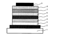
- FIG. 1 is a cross-sectional view schematically showing an example of the structure of the organic electroluminescent element of the present invention.
- the organic electroluminescent device shown in FIG. 1 is configured by laminating an anode, a hole injection layer, a hole transport layer, a light emitting layer, a hole blocking layer, an electron injection layer, and a cathode in this order on a substrate.
- the hole transport layer usually corresponds to the organic compound-containing layer of the present invention described above.
- Substrate serves as a support for the organic electroluminescence device, and quartz or glass plates, metal plates or metal foils, plastic films or sheets are used.
- a glass plate or a transparent synthetic resin plate such as polyester, polymethacrylate, polycarbonate, or polysulfone is preferable.
- a synthetic resin substrate it is necessary to pay attention to gas barrier properties. If the gas barrier property of the substrate is too small, the organic electroluminescent element may be deteriorated by the outside air that has passed through the substrate, which is not preferable. For this reason, a method of providing a gas barrier property by providing a dense silicon oxide film or the like on at least one surface of the synthetic resin substrate is also a preferable method.
- Anode plays a role of hole injection into a layer on the light emitting layer side (hole injection layer, light emitting layer, or the like) described later.
- This anode is usually a metal such as aluminum, gold, silver, nickel, palladium, or platinum, a metal oxide such as an oxide of indium and / or tin, a metal halide such as copper iodide, carbon black, or poly It is composed of conductive polymers such as (3-methylthiophene), polypyrrole and polyaniline.
- the anode is often formed by a sputtering method, a vacuum deposition method, or the like.
- anode can also be formed by coating.
- a thin film can be directly formed on a substrate by electrolytic polymerization, or an anode can be formed by applying a conductive polymer on a substrate (Applied Physics Letters, 1992, Vol. .60, pp. 2711).
- the anode can be formed by stacking different materials. The thickness of the anode varies depending on the required transparency.
- the visible light transmittance is usually 60% or more, preferably 80% or more.
- the thickness is usually 5 nm or more, preferably 10 nm or more, Usually, it is 1000 nm or less, preferably 500 nm or less.
- the anode may be the same as the substrate.
- the anode surface is treated with ultraviolet (UV) / ozone, oxygen plasma, or argon plasma for the purpose of removing impurities adhering to the anode and adjusting the ionization potential to improve hole injection. Is preferred.
- the hole injection layer is a layer that transports holes to a layer adjacent to the cathode side of the anode.
- the organic electroluminescent device of the present invention may have a configuration in which the hole injection layer is omitted.
- the hole injection layer preferably contains a hole transporting compound, and more preferably contains a hole transporting compound and an electron accepting compound.
- the hole injection layer preferably contains a cation radical compound, and particularly preferably contains a cation radical compound and a hole transporting compound.
- the hole injection layer may contain a binder resin and a coating property improving agent as necessary.
- the binder resin is preferably one that does not easily act as a charge trap.
- the hole injection layer can be formed by depositing only the electron-accepting compound on the anode by a wet film formation method, and directly applying and laminating the charge transport material composition thereon. In this case, a part of the charge transport material composition interacts with the electron accepting compound, whereby a layer having excellent hole injecting property is formed.
- the hole transporting compound As the hole transporting compound, a compound having an ionization potential of 4.5 eV to 6.0 eV is preferable. However, when used in the wet film forming method, it is preferable that the solubility in the solvent used in the wet film forming method is high.
- the hole transporting compound is preferably the charge transporting polymer of the present invention from the viewpoint of excellent film forming properties and high charge transporting ability. That is, it is preferable to form a layer using the composition for organic electroluminescent elements of the present invention.
- examples of the hole transporting compound include aromatic amine compounds, phthalocyanine derivatives, porphyrin derivatives, oligothiophene derivatives, polythiophene derivatives, and the like. It is done. Of these, aromatic amine compounds are preferred from the viewpoints of amorphousness and visible light transmittance.
- the type of the aromatic amine compound is not particularly limited, and may be a low molecular compound or a high molecular compound. From the viewpoint of the surface smoothing effect, a polymer having a weight average molecular weight of 1,000 or more and 1,000,000 or less. A compound (polymerizable hydrocarbon compound in which repeating units are continuous) is preferred.
- Preferable examples of the aromatic amine compound may also include an aromatic tertiary amine polymer compound having a repeating unit represented by the following formula (I).
- Ar b1 and Ar b2 are each independently a monovalent aromatic hydrocarbon group which may have a substituent, or an aromatic which may have a substituent.
- Ar b3 to Ar b5 each independently represents a divalent aromatic hydrocarbon group which may have a substituent or an aromatic group which may have a substituent.
- Z b represents a linking group selected from the following group of linking groups, and among Ar b1 to Ar b5 , two groups bonded to the same N atom are bonded to each other. A ring may be formed.
- Ar b6 to Ar b16 are each independently an aromatic hydrocarbon ring which may have a substituent, or an aromatic heterocyclic ring which may have a substituent.
- R b5 and R b6 each independently represents a hydrogen atom or an arbitrary substituent.
- any monovalent or divalent group derived from any aromatic hydrocarbon ring or aromatic heterocyclic ring is applicable. These groups may be the same or different from each other. Further, these groups may further have an arbitrary substituent.
- Specific examples of the aromatic tertiary amine polymer compound having a repeating unit represented by the general formula (I) include compounds described in International Publication No. 2005/089024 pamphlet.
- the hole transporting compound used as the material for the hole injection layer may contain any one of these compounds alone, or may contain two or more. When two or more hole transporting compounds are contained, the combination thereof is arbitrary, but one or more aromatic tertiary amine polymer compounds and one or two other hole transporting compounds are used. It is preferable to use the above together.
- the electron-accepting compound is the same as that described in the section ⁇ Composition for organic electroluminescence device>. The same applies to preferred specific examples.
- cation radical compound an ionic compound composed of a cation radical which is a chemical species obtained by removing one electron from a hole transporting compound and a counter anion is preferable.
- the cation radical is derived from a hole transporting polymer compound
- the cation radical has a structure in which one electron is removed from the repeating unit of the polymer compound.
- the cation radical is preferably a chemical species obtained by removing one electron from the compound described above as the hole transporting compound.
- a chemical species obtained by removing one electron from a compound preferable as a hole transporting compound is preferable in terms of amorphousness, visible light transmittance, heat resistance, solubility, and the like.
- the cation radical compound can be generated by mixing the hole transporting compound and the electron accepting compound. That is, by mixing the hole transporting compound and the electron accepting compound, electron transfer occurs from the hole transporting compound to the electron accepting compound, and the cation radical and the counter anion of the hole transporting compound
- a cation ion compound consisting of Cation radical compounds derived from polymer compounds such as PEDOT / PSS (Adv. Mater., 2000, 12, 481) and emeraldine hydrochloride (J. Phys. Chem., 1990, 94, 7716) It is also produced by oxidative polymerization (dehydrogenation polymerization).
- the oxidative polymerization referred to here is a method in which a monomer is chemically or electrochemically oxidized in an acidic solution using peroxodisulfate or the like.
- a monomer is oxidized to become a polymer, and an anion derived from an acidic solution is used as a counter anion. Generate.
- the hole injection layer can be formed by a wet film formation method or a dry film formation method such as a vacuum evaporation method. In view of excellent film formability, it is preferably formed by a wet film formation method.
- the thickness of the hole injection layer is usually 5 nm or more, preferably 10 nm or more, and usually 1000 nm or less, preferably 500 nm or less.
- the content of the electron-accepting compound in the hole-injecting layer with respect to the hole-transporting compound is usually 0.1 mol% or more, preferably 1 mol% or more. However, it is usually 100 mol% or less, preferably 40 mol% or less.
- hole injection layer As a material for the hole injection layer, other components may be further contained in addition to the above-described hole transporting compound and electron accepting compound as long as the effects of the present invention are not significantly impaired.
- other components include various light emitting materials, electron transporting compounds, binder resins, and coating property improving agents.
- 1 type may be used for another component and it may use 2 or more types together by arbitrary combinations and a ratio.
- At least one of the solvents of the composition for forming a hole injection layer used in the wet film formation method is preferably a compound that can dissolve the constituent material of the hole injection layer.
- the boiling point of this solvent is usually 110 ° C. or higher, preferably 140 ° C. or higher, particularly 200 ° C. or higher, usually 400 ° C. or lower, and preferably 300 ° C. or lower. If the boiling point of the solvent is too low, the drying speed is too high and the film quality may be deteriorated. Further, if the boiling point of the solvent is too high, it is necessary to increase the temperature of the drying process, which may adversely affect other layers and the substrate.
- ether solvents examples include aliphatic ethers such as ethylene glycol dimethyl ether, ethylene glycol diethyl ether, propylene glycol-1-monomethyl ether acetate (PGMEA); 1,2-dimethoxybenzene, 1,3-dimethoxybenzene, anisole , Aromatic ethers such as phenetole, 2-methoxytoluene, 3-methoxytoluene, 4-methoxytoluene, 2,3-dimethylanisole, 2,4-dimethylanisole, and the like.
- aliphatic ethers such as ethylene glycol dimethyl ether, ethylene glycol diethyl ether, propylene glycol-1-monomethyl ether acetate (PGMEA); 1,2-dimethoxybenzene, 1,3-dimethoxybenzene, anisole .
- Aromatic ethers such as phenetole, 2-methoxytoluene, 3-methoxytoluen
- ester solvent examples include aromatic esters such as phenyl acetate, phenyl propionate, methyl benzoate, ethyl benzoate, propyl benzoate, and n-butyl benzoate.
- aromatic hydrocarbon solvent examples include toluene, xylene, cyclohexylbenzene, 3- isopropylpropylphenyl, 1,2,3,4-tetramethylbenzene, 1,4-diisopropylbenzene, cyclohexylbenzene, and methylnaphthalene.
- amide solvent examples include N, N-dimethylformamide and N, N-dimethylacetamide.
- dimethyl sulfoxide and the like can also be used. These solvent may use only 1 type and may use 2 or more types by arbitrary combinations and a ratio.
- the composition After preparing the composition for forming a hole injection layer, the composition is applied onto a layer corresponding to the lower layer of the hole injection layer (usually an anode) by wet film formation and dried to form a hole injection layer.
- the temperature in the film forming step is preferably 10 ° C. or higher, and preferably 50 ° C. or lower in order to prevent film loss due to the formation of crystals in the composition.
- the relative humidity in a film-forming process is not limited unless the effect of this invention is impaired remarkably, it is 0.01 ppm or more normally and 80% or less normally.
- the film of the composition for forming a hole injection layer is usually dried by heating or the like.
- a heating step is usually performed.
- the heating means used in the heating step include a clean oven, a hot plate, an infrared ray, a halogen heater, and microwave irradiation. Among them, a clean oven and a hot plate are preferable in order to uniformly apply heat to the entire film.
- the heating temperature in the heating step is preferably heated at a temperature equal to or higher than the boiling point of the solvent used in the composition for forming a hole injection layer as long as the effects of the present invention are not significantly impaired.
- the heating temperature is preferably equal to or higher than the boiling point of the solvent of the composition for forming a hole injection layer.
- the heating time is not limited as long as sufficient crosslinking of the coating film does not occur, but it is preferably 10 seconds or longer and usually 180 minutes or shorter. If the heating time is too long, the components of the other layers tend to diffuse, and if it is too short, the hole injection layer tends to be inhomogeneous. Heating may be performed in two steps.
- the hole injection layer is formed by vacuum deposition
- one or more of the constituent materials of the hole injection layer (the aforementioned hole transporting compound, electron accepting compound, etc.) are placed in a vacuum container.
- crucibles in case of using two or more kinds of materials, put them in each crucible
- evacuate the inside of the vacuum vessel to about 10 -4 Pa with a suitable vacuum pump, and then heat the crucible (two or more kinds)
- heat each crucible heat each crucible and evaporate by controlling the amount of evaporation (when using two or more materials, evaporate by independently controlling the amount of evaporation) and place it facing the crucible.
- a hole injection layer is formed on the anode of the substrate.
- those hole mixture layers can also be formed by putting them in a crucible and heating and evaporating them.
- the degree of vacuum at the time of vapor deposition is not limited as long as the effects of the present invention are not significantly impaired, but usually 0.1 ⁇ 10 ⁇ 6 Torr (0.13 ⁇ 10 ⁇ 4 Pa) or more, usually 9.0 ⁇ 10 ⁇ 6 Torr. (12.0 ⁇ 10 ⁇ 4 Pa) or less.
- the deposition rate is not limited as long as the effect of the present invention is not significantly impaired, but is usually 0.1 ⁇ / second or more and usually 5.0 ⁇ / second or less.
- the film forming temperature at the time of vapor deposition is not limited as long as the effect of the present invention is not significantly impaired, but is preferably 10 ° C. or higher, preferably 50 ° C. or lower.
- the thickness of the hole injection layer is usually 5 nm or more, preferably 10 nm or more, and usually 1000 nm or less, preferably 500 nm or less.
- the hole transport layer can be formed on the hole injection layer when there is a hole injection layer and on the anode when there is no hole injection layer.
- the organic electroluminescent device of the present invention may have a configuration in which the hole transport layer is omitted.
- the material for forming the hole transport layer is preferably a material having a high hole transport capability and capable of efficiently transporting the injected holes. Therefore, it is preferable that the ionization potential is small, the transparency to visible light is high, the hole mobility is large, the stability is high, and impurities that become traps are not easily generated during manufacturing or use.
- the hole transporting compound the charge transporting polymer of the present invention is particularly preferable from the above point.
- a compound other than the charge transporting polymer of the present invention is used as the hole transporting compound, a material conventionally used as a constituent material of the hole transporting layer can be used. Examples of conventionally used materials include those exemplified as the hole transporting compound used in the above-described hole injection layer.
- aromatic amine compounds having a starburst structure such as aromatic diamines (Japanese Patent Laid-Open No. 5-234811), 4,4 ′, 4 ′′ -tris (1-naphthylphenylamino) triphenylamine (J. Lumin., 72-74, 985, 1997), an aromatic amine compound comprising a tetramer of triphenylamine (Chem.
- Spiro compounds such as tetrakis- (diphenylamino) -9,9′-spirobifluorene (Synth. Metals, 91, 209, 1997), 4,4′-N, N′-dicar Carbazole derivatives such as tetrazole biphenyl.
- polyvinyl carbazole polyvinyl triphenylamine (Japanese Unexamined Patent Publication No. 7-53953), polyarylene ether sulfone containing tetraphenylbenzidine (Polym. Adv. Tech., 7, 33, 1996). Etc.
- a composition for forming a hole transport layer is prepared in the same manner as in the formation of the hole injection layer, and then heated and dried after coating.
- the composition for forming a hole transport layer contains a solvent in addition to the above hole transport compound.
- the solvent used is the same as that used for the composition for forming a hole injection layer.
- the coating conditions, heating and drying conditions, and the like are the same as in the case of forming the hole injection layer.
- the film forming conditions are the same as in the case of forming the hole injection layer.
- the hole transport layer may contain various light emitting materials, electron transport compounds, binder resins, coatability improvers, and the like in addition to the hole transport compound.
- the hole transport layer may also be a layer formed by crosslinking a crosslinkable compound.
- the crosslinkable compound is a compound having a crosslinkable group, and forms a network polymer compound by crosslinking.
- Examples of such crosslinkable groups include cyclic ether groups such as oxetane groups and epoxy groups; groups containing unsaturated double bonds such as vinyl groups, trifluorovinyl groups, styryl groups, acrylic groups, methacryloyl groups, and cinnamoyl groups.
- the crosslinkable compound may be any of a monomer, an oligomer, and a polymer.
- the crosslinkable compound may have only 1 type, and may have 2 or more types by arbitrary combinations and ratios.
- a hole transporting compound having a crosslinkable group is preferably used.
- hole transporting compounds include nitrogen-containing aromatic compound derivatives such as pyridine derivatives, pyrazine derivatives, pyrimidine derivatives, triazine derivatives, quinoline derivatives, phenanthroline derivatives, carbazole derivatives, phthalocyanine derivatives, porphyrin derivatives; triphenylamine derivatives Silole derivatives; oligothiophene derivatives, condensed polycyclic aromatic derivatives, metal complexes and the like.
- nitrogen-containing aromatic derivatives such as pyridine derivatives, pyrazine derivatives, pyrimidine derivatives, triazine derivatives, quinoline derivatives, phenanthroline derivatives, carbazole derivatives; triphenylamine derivatives, silole derivatives, condensed polycyclic aromatic derivatives, metal complexes, etc.
- triphenylamine derivatives particularly preferred are triphenylamine derivatives.
- the composition for forming a hole transport layer may contain an additive for promoting a crosslinking reaction in addition to the crosslinking compound.
- additives that accelerate the crosslinking reaction include polymerization initiators and polymerization accelerators such as alkylphenone compounds, acylphosphine oxide compounds, metallocene compounds, oxime ester compounds, azo compounds, onium salts; condensed polycyclic hydrocarbons, And photosensitizers such as porphyrin compounds and diaryl ketone compounds.
- it may contain a coating property improving agent such as a leveling agent and an antifoaming agent; an electron accepting compound; a binder resin;
- the crosslinkable compound is usually 0.01% by weight or more, preferably 0.05% by weight or more, more preferably 0.1% by weight or more, usually 50% by weight or less, preferably 20%. It is contained by weight% or less, more preferably 10% by weight or less.
- the crosslinkable compound is formed by heating and / or irradiation with active energy such as light. It is crosslinked to form a network polymer compound.
- the thickness of the hole transport layer is usually 5 nm or more, preferably 10 nm or more, and usually 1000 nm or less, preferably 500 nm or less.
- the light emitting layer is formed on the hole transport layer when there is a hole transport layer, and on the hole injection layer when there is no hole transport layer without the hole transport layer. When there is no hole injection layer, it is formed on the anode.
- the light emitting layer may be a layer independent of the hole injection layer, the hole transport layer, and the hole blocking layer, the electron transport layer, etc., which will be described later, but does not form an independent light emitting layer.
- Other organic layers such as a transport layer and an electron transport layer may serve as the light emitting layer.
- the light-emitting layer is formed by directly injecting holes from an anode or through a hole injection layer or a hole transport layer between electrodes to which an electric field is applied, and directly from a cathode, or a cathode buffer layer or an electron transport layer. It is a layer that is excited by recombination with electrons injected through a hole blocking layer or the like and becomes a main light emitting source.
- the light emitting layer can be formed by any method as long as the effects of the present invention are not significantly impaired.
- the light emitting layer is formed on the anode by a wet film forming method or a vacuum deposition method.
- the wet film forming method is preferable.
- the wet film forming method and the vacuum deposition method can be performed using the same method as the hole injection layer.
- the light emitting layer contains at least a material having a light emitting property (light emitting material), and preferably a material having a hole transporting property (hole transporting material) or a material having an electron transporting property (electron). Transport material).
- the light emitting layer may contain other components without departing from the spirit of the present invention. As these materials, it is preferable to use low molecular weight materials from the viewpoint of forming a light emitting layer by a wet film forming method as described later.
- any known material can be applied as the light emitting material.
- a fluorescent material or a phosphorescent material may be used, but a phosphorescent material is preferable from the viewpoint of internal quantum efficiency.
- a phosphorescent material is preferable from the viewpoint of internal quantum efficiency.
- it is also important to reduce the symmetry and rigidity of the molecules of the luminescent material, or to introduce a lipophilic substituent such as an alkyl group.
- a fluorescent dye is not limited to the following illustrations.
- the fluorescent light-emitting material blue fluorescent dye
- examples of the fluorescent light-emitting material (blue fluorescent dye) that emits blue light include naphthalene, chrysene, perylene, pyrene, anthracene, coumarin, p-bis (2-phenylethenyl) benzene, and derivatives thereof.
- fluorescent dyes that give green light emission include quinacridone derivatives, coumarin derivatives, and aluminum complexes such as Al (C 9 H 6 NO) 3 .
- fluorescent light emitting material yellow fluorescent dye
- red fluorescent dyes examples include DCM (4- (dicyanomethyrene) -2-methyl-6- (p-dimethylaminostyryl) -4H-pyran) compounds, benzopyran derivatives, rhodamine derivatives, Examples thereof include benzothioxanthene derivatives and azabenzothioxanthene.
- phosphorescent materials include tris (2-phenylpyridine) iridium, tris (2-phenylpyridine) ruthenium, tris (2-phenylpyridine) palladium, bis (2-phenylpyridine) platinum, tris (2- Phenylpyridine) osmium, tris (2-phenylpyridine) rhenium, octaethylplatinum porphyrin, octaphenylplatinum porphyrin, octaethyl palladium porphyrin, octaphenyl palladium porphyrin, and the like.
- Polymeric light-emitting materials include poly (9,9-dioctylfluorene-2,7-diyl), poly [(9,9-dioctylfluorene-2,7-diyl) -co- (4,4′- (N- (4-sec-butylphenyl)) diphenylamine)], poly [(9,9-dioctylfluorene-2,7-diyl) -co- (1,4-benzo-2 ⁇ 2,1'-3 ⁇ -Triazole)], and polyphenylene vinylene materials such as poly [2-methoxy-5- (2-hexylhexyloxy) -1,4-phenylene vinylene].
- the charge transporting polymer of the present invention can also be used as a light emitting material.
- the molecular weight of the compound used as the light emitting material is arbitrary as long as the effect of the present invention is not significantly impaired, but is usually 10,000 or less, preferably 5000 or less, more preferably 4000 or less, still more preferably 3000 or less, and usually 100 or more, Preferably it is 200 or more, More preferably, it is 300 or more, More preferably, it is the range of 400 or more. If the molecular weight of the luminescent material is too small, the heat resistance will be significantly reduced, gas generation will be caused, the film quality will deteriorate when the film is formed, or the morphology of the organic electroluminescent element will change due to migration, etc. May come.
- the molecular weight of the luminescent material is too large, it tends to be difficult to purify the organic compound, or it may take time to dissolve in the solvent.
- only 1 type may be used for the luminescent material mentioned above, and 2 or more types may be used together by arbitrary combinations and a ratio.
- the ratio of the light emitting material in the light emitting layer is arbitrary as long as the effect of the present invention is not significantly impaired, but is preferably 0.05% by weight or more, and preferably 35% by weight or less. If the amount of the light emitting material is too small, uneven light emission may occur. If the amount is too large, the current efficiency may decrease.
- 2 or more types of luminescent material it is made for the total content of these to be contained in the said range.
- Examples of the low molecular weight hole transport material include various compounds exemplified as the hole transport material of the above-described hole transport layer, and 4,4′-bis [N- (1-naphthyl) -N—.
- Aromatic diamines including two or more tertiary amines, represented by phenylamino] biphenyl, wherein two or more condensed aromatic rings are substituted with nitrogen atoms (Japanese Patent Laid-Open No.
- low molecular weight electron transport materials examples include 2,5-bis (1-naphthyl) -1,3,4-oxadiazole (BND) and 2,5-bis (6 ′-(2 ′, 2 "-bipyridyl))-1,1-dimethyl-3,4-diphenylsilole (PyPySPyPy), bathophenanthroline (BPhen), 2,9-dimethyl-4,7-diphenyl-1,10-phenanthroline (BCP) , Bathocuproin), 2- (4-biphenylyl) -5- (p-tertiarybutylphenyl) -1,3,4-oxadiazole (tBu-PBD) and 4,4′-bis (9-carbazole) -Biphenyl (CBP), 9,10-di- (2-naphthyl) anthracene (ADN) and the like.
- BND 2,5-bis (1-naphthyl)
- hole transport materials and electron transport materials are preferably used as host materials in the light emitting layer.
- Specific examples of the host material include those described in Japanese Unexamined Patent Publication No. 2007-067383, Japanese Unexamined Patent Publication No. 2007-88433, Japanese Unexamined Patent Publication No. 2007-110093, and preferred examples thereof are also the same. It is.
- Examples of the method for forming the light emitting layer include a wet film forming method and a vacuum deposition method. As described above, a homogeneous and defect-free thin film can be easily obtained, and the time required for the formation can be shortened. Furthermore, a wet film-forming method is preferable because the effect of crosslinking the hole transport layer by the organic compound of the present invention can be enjoyed.
- a wet film-forming method is preferable because the effect of crosslinking the hole transport layer by the organic compound of the present invention can be enjoyed.
- a wet film-forming method prepare the coating solution by dissolving the above materials in an appropriate solvent, apply it to the hole transport layer after the above-mentioned formation, coat it, and dry it. Then, it is formed by removing the solvent.
- the formation method is the same as the formation method of the hole transport layer.
- the thickness of the light emitting layer is usually 3 nm or more, preferably 5 nm or more, and usually 300 nm or less, preferably 100
- Hole blocking layer A hole blocking layer 6 may be provided between the light emitting layer 5 and an electron injection layer 8 described later.
- the hole blocking layer 6 is a layer laminated on the light emitting layer 5 so as to be in contact with the interface of the light emitting layer 5 on the cathode 9 side.
- the hole blocking layer 6 has a role of blocking holes moving from the anode 2 from reaching the cathode 9 and a role of efficiently transporting electrons injected from the cathode 9 toward the light emitting layer 5.
- the physical properties required for the material constituting the hole blocking layer 6 include high electron mobility, low hole mobility, a large energy gap (difference between HOMO and LUMO), and excited triplet level (T1). Is high.
- Examples of the hole blocking layer material satisfying such conditions include bis (2-methyl-8-quinolinolato) (phenolato) aluminum, bis (2-methyl-8-quinolinolato) (triphenylsilanolato) aluminum, and the like.
- Triazole derivatives such as styryl compounds (Japanese Patent Laid-Open No. 11-242996), 3- (4-biphenylyl) -4-phenyl-5 (4-tert-butylphenyl) -1,2,4-triazole (Japan) Japanese Patent Laid-Open No. 7-41759), phenanthroline derivatives such as bathocuproine (Japanese Patent Laid-Open No. 10-79297) Broadcast), and the like. Further, a compound having at least one pyridine ring substituted at the 2,4,6-positions described in International Publication No. 2005-022962 is also preferable as a material for the hole blocking layer 6.
- the material of the hole-blocking layer 6 may use only 1 type, and may use 2 or more types together by arbitrary combinations and a ratio. There is no restriction
- FIG. Therefore, it can be formed by a wet film forming method, a vapor deposition method, or other methods.
- the thickness of the hole blocking layer 6 is arbitrary as long as the effect of the present invention is not significantly impaired, but is usually 0.3 nm or more, preferably 0.5 nm or more, and usually 100 nm or less, preferably 50 nm or less.
- Electron transport layer The electron transport layer is provided between the light emitting layer and the electron injection layer for the purpose of further improving the current efficiency of the device.
- the electron transport layer is formed of a compound that can efficiently transport electrons injected from the cathode between electrodes to which an electric field is applied in the direction of the light emitting layer.
- the electron transporting compound used in the electron transporting layer is a compound that has high electron injection efficiency from the cathode or the electron injection layer and has high electron mobility and can efficiently transport injected electrons. It is necessary.
- Materials satisfying such conditions include metal complexes such as aluminum complexes of 8-hydroxyquinoline (Japanese Unexamined Patent Publication No.
- metal complexes of 10-hydroxybenzo [h] quinoline, oxadiazole derivatives Distyrylbiphenyl derivatives, silole derivatives, 3- or 5-hydroxyflavone metal complexes, benzoxazole metal complexes, benzothiazole metal complexes, trisbenzimidazolylbenzene US Pat. No.
- the lower limit of the thickness of the electron transport layer is usually 1 nm, preferably about 5 nm, and the upper limit is usually about 300 nm, preferably about 100 nm.
- the electron transport layer is formed by laminating on the hole blocking layer by a wet film formation method or a vacuum deposition method in the same manner as described above. Usually, a vacuum deposition method is used.
- Electron injection layer plays a role of efficiently injecting electrons injected from the cathode into the electron transport layer or the light emitting layer.
- the material for forming the electron injection layer is preferably a metal having a low work function. Examples include alkali metals such as sodium and cesium, and alkaline earth metals such as barium and calcium.
- the film thickness is usually preferably from 0.1 nm to 5 nm.
- organic electron transport materials represented by metal complexes such as nitrogen-containing heterocyclic compounds such as bathophenanthroline and aluminum complexes of 8-hydroxyquinoline described later are doped with alkali metals such as sodium, potassium, cesium, lithium and rubidium.
- the film thickness in this case is usually in the range of 5 nm or more, preferably 10 nm or more, and usually 200 nm or less, preferably 100 nm or less.
- the electron injection layer is formed by laminating on the light emitting layer or the hole blocking layer thereon by a wet film formation method or a vacuum deposition method. Details of the wet film forming method are the same as those of the hole injection layer and the light emitting layer.
- the vacuum vapor deposition method the vapor deposition source is put into a crucible or a metal boat installed in the vacuum vessel, and the inside of the vacuum vessel is evacuated to about 10 ⁇ 4 Pa with an appropriate vacuum pump, and then the crucible or metal The boat is heated and evaporated to form an electron injection layer on the light emitting layer, hole blocking layer or electron transport layer on the substrate placed facing the crucible or metal boat.
- the alkali metal as the electron injection layer is deposited by using an alkali metal dispenser in which nichrome is filled with an alkali metal chromate and a reducing agent. By heating the dispenser in a vacuum container, the alkali metal chromate is reduced and the alkali metal is evaporated.
- the organic electron transport material and alkali metal are co-evaporated, the organic electron transport material is put in a crucible installed in a vacuum vessel, and the inside of the vacuum vessel is evacuated to about 10 ⁇ 4 Pa with an appropriate vacuum pump.
- Each crucible and dispenser are simultaneously heated and evaporated to form an electron injection layer on the substrate placed facing the crucible and dispenser. At this time, co-evaporation is uniformly performed in the film thickness direction of the electron injection layer, but there may be a concentration distribution in the film thickness direction.
- the cathode plays a role of injecting electrons into a layer on the light emitting layer side (such as an electron injection layer or a light emitting layer).
- a metal having a low work function is preferable, and tin, magnesium, indium, calcium, aluminum, A suitable metal such as silver or an alloy thereof is used.
- Specific examples include low work function alloy electrodes such as magnesium-silver alloy, magnesium-indium alloy, and aluminum-lithium alloy.
- the thickness of the cathode is usually the same as that of the anode.
- metals such as aluminum, silver, copper, nickel, chromium, gold, platinum are used.
- the organic electroluminescent element having the layer configuration shown in FIG. 1 has been described as an example.
- the organic electroluminescent element of the present invention may have another configuration without departing from the gist thereof.
- an arbitrary layer may be provided between the anode and the cathode in addition to the layers described above, and an arbitrary layer may be omitted.
- the charge transporting polymer of the present invention for the hole transport layer, all of the hole injection layer, the hole transport layer and the light emitting layer can be laminated by a wet film formation method. . This makes it possible to manufacture a large area display.
- a cathode, an electron injection layer, a light emitting layer, a hole injection layer, and an anode can be laminated in this order on a substrate, and at least one of them is transparent as described above. It is also possible to provide the organic electroluminescence device of the present invention between two high-height substrates. Further, a structure in which a plurality of layers shown in FIG. 1 are stacked (a structure in which a plurality of light emitting units are stacked) may be employed. In that case, for example, V 2 O 5 or the like is used as the charge generation layer (CGL) instead of the interfacial layer (between the light emitting units) (two layers when the anode is ITO and the cathode is Al).
- CGL charge generation layer
- the present invention can be applied to any of organic electroluminescent elements, a single element, an element having a structure arranged in an array, and a structure in which an anode and a cathode are arranged in an XY matrix.
- Organic EL display and the organic EL illumination of the present invention use the organic electroluminescent element of the present invention as described above.
- organic electroluminescent display of this invention and organic electroluminescent illumination, It can assemble in accordance with a conventional method using the organic electroluminescent element of this invention.
- the organic EL display and the organic EL display of the present invention can be obtained by the method described in “Organic EL display” (Ohm, August 20, 2004, published by Shizushi Tokito, Chiba Adachi, Hideyuki Murata). EL illumination can be formed.
- the target product 2 (2.31 g), tetrahydrofuran 15 mL, and ethanol 15 mL were added to a 100 mL eggplant flask and dissolved.
- 1.07 g of Raney nickel (R-200, manufactured by Nikko Rica Co., Ltd.) was added as a hydrogenation catalyst, and the mixture was replaced with hydrogen three times, followed by reaction at room temperature under hydrogen for 35 hours.
- the reaction solution was filtered through celite and concentrated with an evaporator to obtain 2.8 g of a crude product.
- Potassium fluoride (23.01 g) was charged into the reaction vessel, and heating and drying and nitrogen substitution were repeated under reduced pressure to create a nitrogen atmosphere in the system.
- 3-Nitrophenylboronic acid (6.68 g), 4-bromo-benzocyclobutene (7.32 g) and dehydrated tetrahydrofuran (50 ml) were charged and stirred.
- tris (dibenzylideneacetone) dipalladium chloroform complex (0.21 g)
- the inside of the system was sufficiently purged with nitrogen, and tri-t-butylphosphine (0.47 g) was added at room temperature. Thereafter, the mixture was stirred for 1 hour.
- the target product 8 (8.11 g), tetrahydrofuran 36 ml, ethanol 36 ml, 10% Pd / C (1.15 g) were charged, and the mixture was heated and stirred at 70 ° C. Hydrazine monohydrate (10.81 g) was slowly added dropwise thereto. After reacting for 2 hours, the mixture was allowed to cool, the reaction mixture was filtered through celite, and the filtrate was concentrated. Ethyl acetate was added to the filtrate, washed with water, and the organic layer was concentrated. The resulting crude product was purified by column chromatography (hexane / ethyl acetate) to give the intended product 9 (4.90 g). (Synthesis Example 10)
- the target product 10 (2.89 g), 2,7-dibromofluorene (1.17 g) and dimethyl sulfoxide (30 ml) were placed in a 100 ml four-necked flask and stirred, and the temperature was raised to 60 ° C. Crushed sodium hydroxide (0.72 g) was dissolved in 5 ml of water, dropped into this solution, and reacted for 3 hours. 50 ml of hexane was added to the reaction solution and washed with 30 ml of water. The oil layer was concentrated and subjected to column purification.
- the target product 12 (2.70 g), 1-bromohexane (1.31 g), tetra-n-butylammonium bromide (0.34 g) and dimethyl sulfoxide (30 ml) were added to the reactor, and the temperature was raised to 60 ° C. It returned to room temperature. An aqueous solution (1.2 ml) of sodium hydroxide (0.64 g) was added dropwise. After stirring for 1.5 hours, water (60 ml) and ethyl acetate (100 ml) were added to the reaction solution, the organic layer was concentrated, and the resulting oily component was purified by silica gel chromatography (hexane / methylene chloride). The target product 13 (1.80 g) was obtained. (Synthesis Example 14)
- the desired product 14 (3.64 g), 4-bromoiodobenzene (3.97 g), toluene (60 ml), ethanol (30 ml), 2M aqueous sodium carbonate solution (30 ml) were added to the reactor, and the temperature was raised to 50 ° C. After warming, tetrakis (triphenylphosphine) palladium (0.40 g) was added. The temperature was raised to 80 ° C. and stirred for 8 hours.
- Target 5 (1.086 g, 3.1075 mmol), Target 3 (0.184 g, 0.5984 mmol), aniline (0.197 g, 2.1185 mmol), 4,4′-dibromobiphenyl (0.891 g, 2 .8551 mmol), sodium tert-butoxy (1.76 g, 18.27 mmol) and toluene (23 ml) were charged, and the system was sufficiently purged with nitrogen and heated to 60 ° C. (solution A).
- Tri-t-butylphosphine (0.092 g, 0.457 mmol) was added to a toluene 2 ml solution of tris (dibenzylideneacetone) dipalladium chloroform complex (0.059 g, 0.057 mmol) and heated to 60 ° C. ( Solution B). In a nitrogen stream, solution B was added to solution A, and the mixture was heated to reflux for 1.5 hours. After confirming disappearance of the target compound 5, target compound 3, aniline, and 4,4'-dibromobiphenyl, 4,4'-dibromobiphenyl (0.8375 g, 2.684 mmol) was further added.
- Target 3 (0.1087 g), Target 5 (1.185 g), Target 7 (0.069 g), 9,10-bis (4-bromophenyl) anthracene (1.000 g), and sodium tert-butoxy (1.26 g, toluene (10 ml) was charged, the inside of the system was sufficiently purged with nitrogen, and the mixture was heated to 50 ° C.
- solution E Tris (dibenzylideneacetone) dipalladium chloroform complex (0.042 g) in toluene Tri-t-butylphosphine (0.066 g) was added to a 2 ml solution and heated to 50 ° C.
- Solution F Solution F was added to Solution E in a nitrogen stream and the mixture was heated to 90 ° C. for 1.5 hours. Subsequently, 9,10-bis (4-bromophenyl) anthracene (0.940 g) was further added, and the mixture was heated to reflux for 1 hour, and then the reaction mixture was allowed to cool, and the reaction mixture was stirred with ethanol. The crude polymer 2 was crystallized.
- the obtained crude polymer 2 was dissolved in 150 ml of toluene, bromobenzene (0.52 g) and tert-butoxy sodium (0.63 g) were charged, the inside of the system was sufficiently purged with nitrogen, and the mixture was heated to 50 ° C. ( Solution G).
- Tri-t-butylphosphine (0.033 g) was added to a 2 ml toluene solution of tris (dibenzylideneacetone) dipalladium chloroform complex (0.021 g) and heated to 50 ° C. (solution H). In a nitrogen stream, the solution H was added to the solution G, and the mixture was heated to reflux for 3 hours.
- Diphenylbenzidine (2.07 g, 6.2 mmol), target compound 11 (0.43 g, 0.6 mmol), 9.9′-dihexyl-2,7-dibromofluorene (2.63 g, 5.3 mmol), and tert -Butoxy sodium (2.22 g, 23.0 mmol) and toluene (20 ml) were charged, the inside of the system was sufficiently purged with nitrogen, and the mixture was heated to 50 ° C. (solution I).
- Tri-t-butylphosphine (0.10 g, 0.049 mmol) was added to a 15 ml toluene solution of tris (dibenzylideneacetone) dipalladium chloroform complex (0.07 g, 0.0068 mmol) and heated to 50 ° C. ( Solution J). In a nitrogen stream, solution J was added to solution I, and the mixture was heated to reflux for 1 hour. After confirming the disappearance of diphenylbenzidine, target 11, 9.9′-dihexyl-2,7-dibromofluorene, 9.9′-dihexyl-2,7-dibromofluorene (1.91 g, 6.1 mmol) was confirmed. Was added.
- the obtained crude polymer 3 was dissolved in 100 ml of toluene, bromobenzene (0.97 g, 6.2 mmol) and sodium tert-butoxy (0.710 g, 7 mmol) were charged, and the inside of the system was sufficiently purged with nitrogen. Warmed to 0 ° C. (Solution K). Tri-t-butylphosphine (0.012 g, 0.0062 mmol) was added to a 10 ml toluene solution of tris (dibenzylideneacetone) dipalladium chloroform complex (0.051 g, 0.0049 mmol) and heated to 50 ° C. ( Solution L).
- the solution L was added to the solution K, and the mixture was heated to reflux for 2 hours.
- N, N-diphenylamine (1.041 g, 6.15 mmol) was added to the reaction solution, and the mixture was further heated to reflux for 2 hours.
- the reaction solution was allowed to cool and added dropwise to methanol to obtain an end-capped crude polymer 3.
- This end-capped crude polymer 3 was dissolved in toluene, reprecipitated in acetone, and the precipitated polymer was separated by filtration.
- the obtained polymer was dissolved in toluene, washed with dilute hydrochloric acid, and reprecipitated with ammonia-containing ethanol.
- target 15 (0.659 g), target 16 (1.22 g), aniline (0.516 g), tert-butoxy sodium (1.70 g), and toluene (20 ml) were added to the reactor. Warmed to 50 ° C. (Solution A). Tri-t-butylphosphine (0.089 g) was added to a 1 ml toluene solution of tris (dibenzylideneacetone) dipalladium chloroform complex (0.0057 g) and heated to 50 ° C. (solution B). In a nitrogen stream, solution B was added to solution A and heated to reflux for 1 hour. After confirming disappearance of the raw material, the target product 16 (1.78 g) was added. The reaction was heated to reflux for 40 minutes. The reaction solution was allowed to cool, and the reaction solution was dropped into 200 ml of ethanol to crystallize the crude polymer 4.
- This end-capped crude polymer 4 was dissolved in toluene, washed with dilute hydrochloric acid, and reprecipitated with ammonia-containing ethanol. Then, it melt
- the target product 13 (1.50 g), 2,7-dibromo-9,9-dihexylfluorene (0.683 g), aniline (0.728 g), tert-butoxy sodium (2.41 g) were placed in a reactor. And toluene (15 ml) were added and warmed to 50 ° C. (solution A). Tri-t-butylphosphine (0.126 g) was added to a 1 ml toluene solution of tris (dibenzylideneacetone) dipalladium chloroform complex (0.080 g) and heated to 50 ° C. (solution B). In a nitrogen stream, solution B was added to solution A and heated to reflux for 1 hour.
- Tri-t-butylphosphine (0.16 g, 0.8 mmol) was added to a 6 ml toluene solution of tris (dibenzylideneacetone) dipalladium chloroform complex (0.10 g, 0.1 mmol) and heated to 50 ° C. (solution N ).
- Solution N was added to solution M in a nitrogen stream, and the mixture was heated to reflux for 1 hour. After confirming the disappearance of aniline, target product 9, target product 5, 4,4′-dibromobiphenyl, 4,4′-dibromobiphenyl (1.41 g, 4.5 mmol) was further added.
- the obtained crude polymer 6 was dissolved in 70 ml of toluene, bromobenzene (0.30 g, 1.9 mmol) and tert-butoxy sodium (1.48 g, 15.3 mmol) were charged, and the inside of the system was sufficiently purged with nitrogen. Warmed to 0 ° C. (Solution O). Tri-t-butylphosphine (0.08 g, 0.4 mmol) was added to a 4 ml toluene solution of tris (dibenzylideneacetone) dipalladium chloroform complex (0.05 g, 0.05 mmol) and heated to 50 ° C. (solution P ).
- the solution P was added to the solution O, and the mixture was heated to reflux for 2 hours.
- N, N-diphenylamine (1.63 g, 9.6 mmol) was added to the reaction solution, and the mixture was further heated to reflux for 4 hours.
- the reaction solution was allowed to cool and dropped into an aqueous ethanol solution (ethanol 150 ml + water 25 ml) to obtain end-capped crude polymer 6.
- This end-capped crude polymer 6 was dissolved in toluene, reprecipitated in acetone, and the precipitated polymer was separated by filtration.
- the obtained polymer was dissolved in toluene, washed with dilute hydrochloric acid, and reprecipitated with ammonia-containing ethanol.
- Target 9 (0.1702 g), Target 5 (1.485 g), 9,10-bis (4-bromophenyl) anthracene (1.250 g), tert-butoxy sodium (1.58 g), toluene (12 ml) ),
- the inside of the system was sufficiently substituted with nitrogen, and heated to 50 ° C. (solution Q).
- Tri-t-butylphosphine (0.083 g) was added to a 3 ml toluene solution of tris (dibenzylideneacetone) dipalladium chloroform complex (0.053 g) and heated to 50 ° C. (solution R). In a nitrogen stream, the solution R was added to the solution Q, and the reaction was performed by heating to 90 ° C.
- Tri-t-butylphosphine (0.030 g) was added to a 3 ml toluene solution of tris (dibenzylideneacetone) dipalladium chloroform complex (0.019 g) and heated to 50 ° C. (solution T).
- solution T was added to the solution S in a nitrogen stream, and the mixture was heated to reflux for 2 hours.
- N, N-diphenylamine (0.30 g) was added, and the solution T prepared again was added, and the mixture was further heated to reflux for 5 hours.
- the reaction solution was allowed to cool and dropped into ethanol to obtain an end-capped crude polymer 7.
- ⁇ Composition for organic electroluminescence device Solvent Toluene Solid content concentration 1.0% by weight
- ⁇ Composition for organic electroluminescence device Solvent Toluene Solid content concentration 1.0% by weight
- the film thus obtained was measured for a fluorescence spectrum at an excitation light wavelength of 375 nm using a spectrophotometer F-4500 (manufactured by Hitachi, Ltd.). As a result, the wavelength at which the fluorescence intensity was maximum was 462 nm. It was.
- Table 1 shows the fluorescence wavelengths of the films prepared in Reference Example 1 and Comparative Reference Example 1.
- the film formed using the charge transporting polymer of the present invention has a fluorescence wavelength on the short wavelength side. That is, it can be seen that the film formed using the charge transporting polymer of the present invention has little uneven aggregation.
- the organic electroluminescent element shown in FIG. 1 was produced.
- An anode was formed by patterning into a stripe having a width of 2 mm.
- the patterned ITO substrate is cleaned in the order of ultrasonic cleaning with an aqueous surfactant solution, water cleaning with ultrapure water, ultrasonic cleaning with ultrapure water, and water cleaning with ultrapure water, followed by drying with compressed air, and finally UV irradiation. Ozone cleaning was performed.
- a hole-transporting polymer material having a repeating structure represented by the following structural formula (P1) (weight average molecular weight: 26500, number-average molecular weight: 12000), 4-isopropyl-4 ′-represented by the structural formula (A1)
- P1 weight average molecular weight: 26500, number-average molecular weight: 12000
- a composition for a hole injection layer containing methyldiphenyliodonium tetrakis (pentafluorophenyl) borate and ethyl benzoate was prepared. This composition was applied onto the anode by spin coating under the following conditions to obtain a hole injection layer having a thickness of 30 nm.
- a composition for an organic electroluminescence device containing the charge transporting polymer (H1) of the present invention (target polymer 1 synthesized in Polymer Synthesis Example 1) represented by the following structural formula was prepared, and the conditions were as follows.
- a hole transport layer having a thickness of 20 nm was formed by coating by spin coating and crosslinking by heating.
- ⁇ Composition for organic electroluminescence device Solvent Toluene Composition concentration 0.4% by weight
- ⁇ Hole transport layer deposition conditions Spinner speed 1500rpm Spinner rotation time 30 seconds Spin coat atmosphere In nitrogen Heating conditions In nitrogen, 230 ° C, 1 hour
- the following organic electroluminescent element composition is prepared using the organic compounds (C1) and (D1) shown below, and is formed on the hole transporting layer under the conditions shown below.
- a light emitting layer was obtained with a film thickness of 40 nm by spin coating.
- the substrate on which the light emitting layer has been formed is transferred into a vacuum vapor deposition apparatus connected to a nitrogen glove box, exhausted until the degree of vacuum in the apparatus becomes 1.7 ⁇ 10 ⁇ 4 Pa or less, and then BAlq (C2) was laminated by a vacuum deposition method to obtain a hole blocking layer.
- the deposition rate was controlled in the range of 0.5 to 1.1 liters / second, and a hole blocking layer having a thickness of 10 nm was formed by laminating on the light emitting layer.
- the degree of vacuum during deposition was 2.6 to 3.9 ⁇ 10 ⁇ 5 Pa.
- Alq3 (C3) was heated and vapor-deposited, and the electron carrying layer was formed into a film.
- the degree of vacuum during deposition is 2.8 to 3.7 ⁇ 10 ⁇ 5 Pa, the deposition rate is controlled in the range of 0.7 to 1.2 liters / second, and a 30 nm thick film is formed on the hole blocking layer.
- the electron transport layer was formed by laminating.
- the element that has been vapor-deposited up to the electron transport layer is transported in a vacuum to a chamber connected to the chamber in which the hole-blocking layer and the electron transport layer are vapor-deposited, and a 2 mm wide stripe as a mask for cathode vapor deposition.
- a thin shadow mask was adhered to the element so as to be orthogonal to the ITO stripe of the anode.
- the electron injection layer first, lithium fluoride (LiF) was controlled using a molybdenum boat at a deposition rate of 0.09 to 0.14 liters / second and a degree of vacuum of 2.7 to 5.4 ⁇ 10 ⁇ 5 Pa. A film having a thickness of 0.5 nm was formed on the electron transport layer.
- aluminum as a cathode is similarly heated by a molybdenum boat and controlled at a deposition rate of 0.5 to 1.3 liters / second and a degree of vacuum of 2.1 to 5.4 ⁇ 10 ⁇ 5 Pa. An aluminum layer was formed. The substrate temperature during the above two-layer deposition was kept at room temperature.
- a sealing process was performed by the method described below.
- a photocurable resin 30Y-437 manufactured by ThreeBond
- a moisture getter sheet manufactured by Dynic
- finished cathode formation was bonded together so that the vapor-deposited surface might oppose a desiccant sheet.
- Example 1 the organic electroluminescent element shown in FIG. 1 was produced in the same manner as Example 1 except that the hole transport layer was formed as follows.
- a composition for an organic electroluminescence device containing a compound (H2) represented by the following structural formula (Comparative Polymer 1 synthesized in Synthesis Example 1 for Comparative Polymer) was prepared, applied by spin coating under the following conditions, and heated.
- the hole transport layer having a film thickness of 20 nm was formed by cross-linking.
- ⁇ Composition for organic electroluminescence device Solvent Toluene Composition concentration 0.4% by weight
- ⁇ Hole transport layer deposition conditions Spinner speed 1500rpm Spinner rotation time 30 seconds Spin coat atmosphere In nitrogen Heating conditions In nitrogen, 230 ° C, 1 hour
- the light emission characteristics of the organic electroluminescent element having a light emitting area portion of 2 mm ⁇ 2 mm obtained in this way are as follows.
- Luminance at 10 mA / cm 2 energization 4663 cd / m 2 Voltage at 10 mA / cm 2 energization: 7.5V Power efficiency at 100 cd / m 2 : 0.9 lm / W
- the maximum wavelength of the emission spectrum of the device was 465 nm, and it was identified as that from the compound (D1).
- Table 2 shows that the organic electroluminescence device having a layer formed by crosslinking the charge transporting polymer of the present invention has a low driving voltage, high power efficiency, and a long driving life.
- Example 2 The organic electroluminescent element shown in FIG. 1 was produced in the same manner as in Example 1 except that the hole transport layer and the light emitting layer were formed as follows in Example 1.
- a composition for an organic electroluminescent device containing the charge transporting polymer (H3) according to the present invention (target polymer 2 synthesized in Polymer Synthesis Example 2) represented by the following structural formula was prepared and spin-coated under the following conditions: And a hole transport layer having a thickness of 20 nm was formed by crosslinking by heating.
- ⁇ Composition for organic electroluminescence device Solvent Toluene Composition concentration 0.4% by weight
- ⁇ Hole transport layer deposition conditions Spinner speed 1500rpm Spinner rotation time 30 seconds Spin coat atmosphere In nitrogen Heating conditions In nitrogen, 230 ° C, 1 hour
- the organic compound (C4) and (D1) shown below are used to prepare the organic electroluminescent element composition shown below, and on the hole transport layer under the conditions shown below.
- a light emitting layer was obtained with a film thickness of 40 nm by spin coating.
- Luminance at 10 mA / cm 2 energization 9477 cd / m 2 Voltage at 10 mA / cm 2 energization: 7.5V Power efficiency at 100 cd / m 2 : 2.0 lm / W
- the maximum wavelength of the emission spectrum of the device was 465 nm, and it was identified as that from the compound (D1).
- Example 2 the organic electroluminescent element shown in FIG. 1 was produced in the same manner as in Example 2 except that the hole transport layer was formed as follows.
- a composition for an organic electroluminescence device containing a compound (H4) represented by the following structural formula (Comparative Polymer 2 synthesized in Synthesis Example 2 for Comparative Polymer) was prepared, applied by spin coating under the following conditions, and heated.
- the hole transport layer having a film thickness of 20 nm was formed by cross-linking.
- ⁇ Composition for organic electroluminescence device Solvent Toluene Composition concentration 0.4% by weight
- ⁇ Hole transport layer deposition conditions Spinner speed 1500rpm Spinner rotation time 30 seconds Spin coat atmosphere In nitrogen Heating conditions In nitrogen, 230 ° C, 1 hour
- the light emission characteristics of the organic electroluminescent element having a light emitting area portion of 2 mm ⁇ 2 mm obtained in this way are as follows.
- Luminance at 10 mA / cm 2 energization 8670 cd / m 2 10mA / cm 2 current at the time of the voltage: 7.4V Power efficiency at 100 cd / m 2 : 1.8 lm / W
- the maximum wavelength of the emission spectrum of the device was 464 nm, which was identified as that from the compound (D1).
- Table 3 shows that the organic electroluminescent device having a layer formed by crosslinking the charge transporting polymer of the present invention has high power efficiency and a long driving life.
- Example 3 the organic electroluminescent element shown in FIG. 1 was produced in the same manner as in Example 2 except that the hole transport layer was formed as follows.
- a composition for an organic electroluminescent device containing the charge transporting polymer (H5) according to the present invention (target polymer 4 synthesized in Polymer Synthesis Example 4) represented by the following structural formula was prepared, and spin was performed under the following conditions.
- a hole transport layer having a thickness of 20 nm was formed by coating by coating and crosslinking by heating.
- ⁇ Composition for organic electroluminescence device Solvent Toluene Composition concentration 0.4% by weight
- ⁇ Hole transport layer deposition conditions Spinner speed 1500rpm Spinner rotation time 30 seconds Spin coating atmosphere Heating condition in nitrogen Heating condition in nitrogen, 230 ° C., 1 hour
- the organic electroluminescence device having a light emitting area portion of 2 mm ⁇ 2 mm obtained in this way has the following emission characteristics. is there.
- Example 3 The organic electroluminescent element shown in FIG. 1 was produced in the same manner as in Example 3 except that the hole transport layer was formed as follows in Example 3.
- the hole transport layer having a thickness of 20 nm was formed by coating by spin coating and crosslinking by heating.
- ⁇ Composition for organic electroluminescence device Solvent Toluene Composition concentration 0.4% by weight
- ⁇ Hole transport layer deposition conditions Spinner speed 1500rpm Spinner rotation time 30 seconds Spin coating atmosphere Heating condition in nitrogen Heating condition in nitrogen, 230 ° C., 1 hour
- the organic electroluminescence device having a light emitting area portion of 2 mm ⁇ 2 mm obtained in this way has the following emission characteristics. is there.
- Table 4 shows that the organic electroluminescent device having a layer formed by crosslinking the charge transporting polymer of the present invention has a low driving voltage, high current efficiency, and a long life.
- Example 4 the organic electroluminescent element shown in FIG. 1 was produced in the same manner as in Example 2 except that the hole transport layer was formed as follows.
- a composition for an organic electroluminescent device containing the charge transporting polymer (H7) according to the present invention (target polymer 3 synthesized in Polymer Synthesis Example 3) represented by the following structural formula was prepared, and spin was performed under the following conditions.
- a hole transport layer having a thickness of 20 nm was formed by coating by coating and crosslinking by heating.
- ⁇ Composition for organic electroluminescence device Solvent Toluene Composition concentration 0.4% by weight
- ⁇ Hole transport layer deposition conditions Spinner speed 1500rpm Spinner rotation time 30 seconds Spin coating atmosphere Heating condition in nitrogen Heating condition in nitrogen, 230 ° C., 1 hour
- the organic electroluminescence device having a light emitting area portion of 2 mm ⁇ 2 mm obtained in this way has the following emission characteristics. is there. Voltage at 100 cd / m 2 : 5.6V Current efficiency at 100 cd / m 2 : 2.6 cd / A
- the maximum wavelength of the emission spectrum of the device was 465 nm, and it was identified as that from the compound (D1).
- Example 4 the organic electroluminescent element shown in FIG. 1 was produced in the same manner as in Example 4 except that the hole transport layer was formed as follows.
- a composition for an organic electroluminescent device containing a charge transporting polymer (H8) (Mw: 55000, Mn: 28900, Mw / Mn: 1.9) represented by the following structural formula was prepared, and spin was performed under the following conditions.
- a hole transport layer having a thickness of 20 nm was formed by coating by coating and crosslinking by heating.
- ⁇ Composition for organic electroluminescence device Solvent Toluene Composition concentration 0.4% by weight
- ⁇ Hole transport layer deposition conditions Spinner speed 1500rpm Spinner rotation time 30 seconds Spin coating atmosphere Heating condition in nitrogen Heating condition in nitrogen, 230 ° C., 1 hour
- the organic electroluminescence device having a light emitting area portion of 2 mm ⁇ 2 mm obtained in this way has the following emission characteristics. is there. Voltage at 100 cd / m 2 : 5.8V Current efficiency at 100 cd / m 2 : 2.2 cd / A
- the maximum wavelength of the emission spectrum of the device was 467 nm, which was identified as from the compound (D1).
- Table 5 shows that the organic electroluminescence device having a layer formed by crosslinking the charge transporting polymer of the present invention has a low driving voltage, high current efficiency, and a long driving life.
- Example 5 A measuring element having a single-layer structure was produced in the manner described below.
- ITO indium tin oxide
- the patterned ITO substrate is cleaned in the order of ultrasonic cleaning with an aqueous surfactant solution, water cleaning with ultrapure water, ultrasonic cleaning with ultrapure water, and water cleaning with ultrapure water, followed by drying with compressed air, and finally UV irradiation. Ozone cleaning was performed.
- the spinner rotation speed was 1500 rpm, and the spinner time was 30 seconds. After spin coating, it was heated at 230 ° C. for 1 hour in an oven at atmospheric pressure. In this way, a sample layer (corresponding to a hole injection layer of an organic electroluminescence device) 10 was formed.
- a stripe shadow mask having a width of 2 mm as a mask for cathode vapor deposition was brought into close contact with the element so as to be orthogonal to the ITO stripe of the anode 2.
- the apparatus was evacuated with a cryopump until the degree of vacuum in the apparatus was 3 ⁇ 10 ⁇ 4 Pa or less.
- Aluminum was heated as a cathode 9 by a molybdenum boat, and an aluminum layer having a thickness of 80 nm was formed by controlling the deposition rate at 0.5 to 5 liters / second and the degree of vacuum at 2 to 3 ⁇ 10 ⁇ 4 Pa.
- the substrate temperature during the deposition of the cathode 9 was kept at room temperature.
- a measuring element having an element area of 2 mm ⁇ 2 mm was obtained.
- the obtained measurement element was connected to a 2400 type source meter (manufactured by Keithley), and voltage was sequentially applied to read the current value.
- the voltage at a current density of 100 mA / cm 2 showed a low value of 5.6V.
- the obtained measurement element was connected to a 2400 type source meter (manufactured by Keithley), and voltage was sequentially applied to read the current value. As a result, the voltage at a current density of 100 mA / cm 2 was 8.3V. It can be seen that the organic electroluminescent device containing an electron accepting compound in the layer formed by crosslinking the charge transporting polymer of the present invention has a low driving voltage.
- the charge transporting polymer of the present invention has a hole injection material, a hole transporting material, an excellent electrochemical stability, film forming property, charge transporting ability, light emitting property, and heat resistance according to the layer structure of the device. It can also be applied as a light emitting material, a host material, an electron injection material, an electron transport material and the like.
- the organic electroluminescent device having a layer (crosslinked layer) obtained by crosslinking the charge transporting polymer of the present invention is a flat panel display (for example, for OA computers or wall-mounted televisions), an in-vehicle display device, a mobile phone display or surface light emission.
- the charge transporting polymer of the present invention has essentially excellent redox stability, it is useful not only for organic electroluminescent devices but also for organic devices such as electrophotographic photoreceptors and organic solar cells. .
Landscapes
- Chemical & Material Sciences (AREA)
- Polymers & Plastics (AREA)
- Engineering & Computer Science (AREA)
- Materials Engineering (AREA)
- Chemical Kinetics & Catalysis (AREA)
- Medicinal Chemistry (AREA)
- Health & Medical Sciences (AREA)
- Organic Chemistry (AREA)
- Physics & Mathematics (AREA)
- Spectroscopy & Molecular Physics (AREA)
- Inorganic Chemistry (AREA)
- Optics & Photonics (AREA)
- Electroluminescent Light Sources (AREA)
- Macromolecular Compounds Obtained By Forming Nitrogen-Containing Linkages In General (AREA)
- Polyoxymethylene Polymers And Polymers With Carbon-To-Carbon Bonds (AREA)
Abstract
Priority Applications (3)
| Application Number | Priority Date | Filing Date | Title |
|---|---|---|---|
| US13/058,675 US8610112B2 (en) | 2008-08-11 | 2009-08-10 | Charge-transporting polymer, composition for organic electroluminescent element, organic electroluminescent element, organic EL display, and organic EL lighting |
| EP09806704.4A EP2314639B1 (fr) | 2008-08-11 | 2009-08-10 | Polymère transporteur de charges, composition pour élément électroluminescent organique, élément électroluminescent organique, dispositif d affichage électroluminescent organique et dispositif d éclairage électroluminescent organique |
| CN2009801287843A CN102105511B (zh) | 2008-08-11 | 2009-08-10 | 电荷传输性聚合物、有机场致发光元件用组合物、有机场致发光元件、有机el显示器及有机el照明 |
Applications Claiming Priority (2)
| Application Number | Priority Date | Filing Date | Title |
|---|---|---|---|
| JP2008207411 | 2008-08-11 | ||
| JP2008-207411 | 2008-08-11 |
Publications (1)
| Publication Number | Publication Date |
|---|---|
| WO2010018813A1 true WO2010018813A1 (fr) | 2010-02-18 |
Family
ID=41668957
Family Applications (1)
| Application Number | Title | Priority Date | Filing Date |
|---|---|---|---|
| PCT/JP2009/064134 WO2010018813A1 (fr) | 2008-08-11 | 2009-08-10 | Polymère transporteur de charges, composition pour élément électroluminescent organique, élément électroluminescent organique, dispositif d’affichage électroluminescent organique et dispositif d’éclairage électroluminescent organique |
Country Status (7)
| Country | Link |
|---|---|
| US (1) | US8610112B2 (fr) |
| EP (1) | EP2314639B1 (fr) |
| JP (2) | JP5491796B2 (fr) |
| KR (1) | KR101619556B1 (fr) |
| CN (1) | CN102105511B (fr) |
| TW (1) | TWI447143B (fr) |
| WO (1) | WO2010018813A1 (fr) |
Cited By (14)
| Publication number | Priority date | Publication date | Assignee | Title |
|---|---|---|---|---|
| JP2012153742A (ja) * | 2011-01-21 | 2012-08-16 | Mitsubishi Chemicals Corp | 重合体、有機電界発光素子材料、有機電界発光素子用組成物、有機電界発光素子、有機el表示装置及び有機el照明 |
| WO2012157211A1 (fr) | 2011-05-13 | 2012-11-22 | ソニー株式会社 | Dispositif électroluminescent organique d'émission de lumière à couleurs multiples |
| WO2013035275A1 (fr) | 2011-09-09 | 2013-03-14 | 出光興産株式会社 | Composé cyclique hétéroaromatique contenant de l'azote |
| WO2013046635A1 (fr) | 2011-09-28 | 2013-04-04 | 出光興産株式会社 | Substance pour élément électroluminescent organique, et élément électroluminescent organique produit en utilisant celle-ci |
| WO2013069242A1 (fr) | 2011-11-07 | 2013-05-16 | 出光興産株式会社 | Matière pour éléments électroluminescents organiques et élément électroluminescent organique l'utilisant |
| US20130270535A1 (en) * | 2010-10-19 | 2013-10-17 | Sumitomo Chemical Company Limited | Polymer and organic light-emitting device |
| WO2013191137A1 (fr) | 2012-06-18 | 2013-12-27 | 三菱化学株式会社 | Composé polymère, polymère transporteur de charge, composition pour éléments électroluminescents organiques, élément électroluminescent organique, dispositif d'affichage el organique, et éclairage el organique |
| JP2014019755A (ja) * | 2012-07-13 | 2014-02-03 | Hitachi Chemical Co Ltd | 硬化性重合体並びにこれを用いた樹脂及び有機el素子 |
| KR20160067847A (ko) | 2013-10-04 | 2016-06-14 | 미쓰비시 가가꾸 가부시키가이샤 | 중합체, 유기 전계 발광 소자용 조성물, 유기 전계 발광 소자, 유기 el 표시 장치 및 유기 el 조명 |
| JP2017002287A (ja) * | 2015-06-05 | 2017-01-05 | 三菱化学株式会社 | 重合体、有機電界発光素子用組成物、有機電界発光素子、有機el表示装置及び有機el照明 |
| WO2017047644A1 (fr) * | 2015-09-18 | 2017-03-23 | 住友化学株式会社 | Composé polymère et élément électroluminescent utilisant ce dernier |
| US9741934B2 (en) | 2014-03-25 | 2017-08-22 | Sumitomo Chemical Company, Limited | Polymer compound and light emitting device using the same |
| US10193069B2 (en) * | 2011-06-27 | 2019-01-29 | Nippon Steel & Sumikin Chemical Co., Ltd. | Polymer for use in organic electroluminescent element and organic electroluminescent element employing same |
| JP2019520455A (ja) * | 2016-06-28 | 2019-07-18 | ダウ グローバル テクノロジーズ エルエルシー | 有機電荷輸送フィルムを作製するためのプロセス |
Families Citing this family (42)
| Publication number | Priority date | Publication date | Assignee | Title |
|---|---|---|---|---|
| KR101415444B1 (ko) * | 2008-04-02 | 2014-07-04 | 미쓰비시 가가꾸 가부시키가이샤 | 고분자 화합물, 그 고분자 화합물을 가교시켜 이루어지는 그물 형상 고분자 화합물, 유기 전계 발광 소자용 조성물, 유기 전계 발광 소자, 유기 el 디스플레이 및 유기 el 조명 |
| WO2012003485A2 (fr) * | 2010-07-02 | 2012-01-05 | Plextronics, Inc. | Compositions de transport de trous et dispositifs et procédés associés (i) |
| JP5720191B2 (ja) * | 2010-11-12 | 2015-05-20 | 三菱化学株式会社 | アリールアミンポリマー、電荷輸送材料、有機電界発光素子用組成物、有機電界発光素子、有機el表示装置及び有機el照明 |
| JP2012111719A (ja) * | 2010-11-25 | 2012-06-14 | Idemitsu Kosan Co Ltd | 重合性単量体、その重合体を含む有機デバイス用材料、正孔注入輸送材料及び有機エレクトロルミネッセンス素子用材料、並びに有機エレクトロルミネッセンス素子 |
| US9676900B2 (en) * | 2011-01-31 | 2017-06-13 | Cambridge Display Technology, Ltd. | Fluorene containing copolymer used in light emitting devices |
| KR20130024040A (ko) * | 2011-08-30 | 2013-03-08 | 삼성디스플레이 주식회사 | 광 발광 다이오드 및 이를 포함하는 광 발광 표시 장치 |
| JP5392438B1 (ja) | 2012-02-23 | 2014-01-22 | 三菱化学株式会社 | 重合体及び有機電界発光素子 |
| JP5955946B2 (ja) | 2012-03-27 | 2016-07-20 | 住友化学株式会社 | 高分子化合物およびそれを用いた発光素子 |
| CN103833988B (zh) * | 2012-11-27 | 2016-08-03 | 海洋王照明科技股份有限公司 | 含蒽-噻咯并二(苯并噻二唑)共聚物及其制备方法和应用 |
| GB2509718A (en) * | 2013-01-09 | 2014-07-16 | Cambridge Display Tech Ltd | Method for forming a layer of an electronic device and appropriate precursor compounds |
| US10665786B2 (en) | 2013-03-08 | 2020-05-26 | Hitachi Chemical Company, Ltd. | Treatment liquid containing ionic compound, organic electronic element, and method for producing organic electronic element |
| US9735378B2 (en) * | 2013-09-09 | 2017-08-15 | Universal Display Corporation | Organic electroluminescent materials and devices |
| EP3131131B1 (fr) * | 2014-04-09 | 2021-08-25 | Sumitomo Chemical Company Limited | Élément électroluminescent et composition utilisée dedans |
| GB2528099A (en) * | 2014-07-09 | 2016-01-13 | Cambridge Display Tech Ltd | Compound |
| WO2016026122A1 (fr) * | 2014-08-21 | 2016-02-25 | Dow Global Technologies Llc | Compositions dérivées de benzocyclobutènes, et dispositifs électroniques les contenant |
| WO2016026123A1 (fr) | 2014-08-21 | 2016-02-25 | Dow Global Technologies Llc | Compositions comprenant des benzocyclobutènes substitués par de l'oxygène et des diénophiles et dispositifs électroniques contenant celles-ci |
| US10297755B2 (en) | 2014-08-21 | 2019-05-21 | Dow Global Technologies Llc | Oxygen substituted benzoclobutenes derived compositions for electronic devices |
| JP6613298B2 (ja) | 2014-08-21 | 2019-11-27 | ダウ グローバル テクノロジーズ エルエルシー | ポリマー電荷移送層及びそれを含む有機電子装置 |
| CN106715520B (zh) * | 2014-09-25 | 2019-05-14 | 住友化学株式会社 | 高分子化合物和使用该高分子化合物的发光元件 |
| KR20170066442A (ko) * | 2014-09-30 | 2017-06-14 | 스미또모 가가꾸 가부시키가이샤 | 발광 소자 |
| GB201418876D0 (en) * | 2014-10-23 | 2014-12-03 | Cambridge Display Tech Ltd | Organic light emitting device |
| JP6779881B2 (ja) * | 2014-12-30 | 2020-11-04 | メルク、パテント、ゲゼルシャフト、ミット、ベシュレンクテル、ハフツングMerck Patent GmbH | 少なくとも1つのポリマーおよび少なくとも1つの金属錯体を含んでなる組成物、ならびにその組成物を含むエレクトロルミネッセンス素子 |
| KR102496777B1 (ko) * | 2015-02-25 | 2023-02-06 | 미쯔비시 케미컬 주식회사 | 중합체, 유기 전계 발광 소자용 조성물, 유기 전계 발광 소자, 유기 el 표시 장치 및 유기 el 조명 |
| JP2017139342A (ja) * | 2016-02-04 | 2017-08-10 | 日立化成株式会社 | 有機発光素子 |
| WO2018083801A1 (fr) | 2016-11-07 | 2018-05-11 | 日立化成株式会社 | Matériau et élément électroniques organiques, couche organique, élément électroluminescent organique, dispositif d'éclairage, et élément et dispositif d'affichage |
| JP6972589B2 (ja) * | 2017-03-15 | 2021-11-24 | 昭和電工マテリアルズ株式会社 | 有機エレクトロニクス材料、及び該材料を用いた有機層、有機エレクトロニクス素子、有機エレクトロルミネセンス素子、表示素子、照明装置、及び表示装置 |
| EP3489276A4 (fr) * | 2016-07-25 | 2020-03-18 | Hitachi Chemical Co., Ltd. | Matériau électronique organique et son utilisation |
| CN108198954B (zh) * | 2016-12-08 | 2019-10-25 | 昆山国显光电有限公司 | 有机电致发光器件及其制备方法、显示装置 |
| CN108183172B (zh) * | 2016-12-08 | 2019-10-25 | 昆山国显光电有限公司 | 有机电致发光器件及其制备方法、显示装置 |
| CN110291157B (zh) * | 2017-02-08 | 2022-05-13 | 昭和电工材料株式会社 | 电荷传输性材料及其用途 |
| EP3591727A4 (fr) | 2017-03-02 | 2020-12-23 | Hitachi Chemical Co., Ltd. | Matériau électronique organique et son utilisation |
| JP2018203889A (ja) * | 2017-06-06 | 2018-12-27 | 日立化成株式会社 | 硬化性重合体、重合液、導電性膜及び有機発光素子 |
| EP3703144A4 (fr) * | 2017-10-27 | 2021-06-30 | Hitachi Chemical Company, Ltd. | Polymère de transport de charge et élément électronique organique |
| WO2019097714A1 (fr) * | 2017-11-20 | 2019-05-23 | 日立化成株式会社 | Procédé de fabrication d'un film mince organique, film mince organique et son utilisation |
| JPWO2019176693A1 (ja) * | 2018-03-15 | 2021-02-25 | 国立大学法人広島大学 | 骨外組織における骨形成関連因子又は石灰化関連因子の発現抑制剤 |
| TW201946309A (zh) * | 2018-03-23 | 2019-12-01 | 日商日鐵化學材料股份有限公司 | 有機電致發光元件用聚合物及有機電致發光元件 |
| TW201942326A (zh) * | 2018-03-27 | 2019-11-01 | 日商日鐵化學材料股份有限公司 | 有機電場發光元件用材料及有機電場發光元件 |
| KR20210002570A (ko) * | 2018-04-26 | 2021-01-08 | 스미또모 가가꾸 가부시키가이샤 | 블록 공중합체 및 그것을 사용한 발광 소자 |
| JP7193953B2 (ja) * | 2018-08-24 | 2022-12-21 | 住友化学株式会社 | 有機elデバイスの製造方法及び有機elデバイス |
| TW202110935A (zh) * | 2019-04-16 | 2021-03-16 | 德商麥克專利有限公司 | 含有可交聯聚合物之調配物 |
| KR102382285B1 (ko) * | 2020-08-25 | 2022-04-04 | 한국생산기술연구원 | 가교결합성 벤조시클로부텐기를 갖는 유기전기소자용 화합물, 이를 이용한 유기전기소자 및 그 전자 장치 |
| CN114334262B (zh) * | 2022-01-24 | 2023-06-27 | 安徽鸿海电缆有限公司 | 一种氟塑料绝缘硅橡胶护套耐高温控制电缆 |
Citations (32)
| Publication number | Priority date | Publication date | Assignee | Title |
|---|---|---|---|---|
| JPS59194393A (ja) | 1983-03-25 | 1984-11-05 | イ−ストマン コダツク カンパニ− | 改良された電力転換効率をもつ有機エレクトロルミネツセント装置 |
| JPH05234681A (ja) | 1990-07-26 | 1993-09-10 | Eastman Kodak Co | 有機エレクトロルミネセンス媒体を有するエレクトロルミネセンス装置 |
| JPH05331459A (ja) | 1992-04-03 | 1993-12-14 | Pioneer Electron Corp | 有機エレクトロルミネッセンス素子 |
| JPH06207169A (ja) | 1992-11-17 | 1994-07-26 | Idemitsu Kosan Co Ltd | 有機エレクトロルミネッセンス素子 |
| JPH0741759A (ja) | 1993-03-26 | 1995-02-10 | Sumitomo Electric Ind Ltd | 有機エレクトロルミネッセンス素子 |
| JPH0753953A (ja) | 1993-08-19 | 1995-02-28 | Mitsubishi Chem Corp | 有機電界発光素子 |
| US5645948A (en) | 1996-08-20 | 1997-07-08 | Eastman Kodak Company | Blue organic electroluminescent devices |
| JPH1079297A (ja) | 1996-07-09 | 1998-03-24 | Sony Corp | 電界発光素子 |
| JPH10270171A (ja) | 1997-01-27 | 1998-10-09 | Junji Kido | 有機エレクトロルミネッセント素子 |
| JPH11242996A (ja) | 1998-02-25 | 1999-09-07 | Mitsubishi Chemical Corp | 有機電界発光素子 |
| JPH11251067A (ja) | 1998-03-02 | 1999-09-17 | Junji Kido | 有機エレクトロルミネッセント素子 |
| JP2001223084A (ja) | 2000-02-07 | 2001-08-17 | Junji Kido | 有機電界発光素子 |
| WO2002010129A2 (fr) | 2000-08-01 | 2002-02-07 | Covion Organic Semiconductors Gmbh | Materiaux structurables, leur procede de fabrication et leur utilisation |
| JP2002100478A (ja) | 2000-09-20 | 2002-04-05 | Mitsubishi Chemicals Corp | 有機電界発光素子及びその製造方法 |
| JP2002100482A (ja) | 2000-09-20 | 2002-04-05 | Mitsubishi Chemicals Corp | 有機電界発光素子 |
| JP2003031365A (ja) | 2001-05-02 | 2003-01-31 | Junji Kido | 有機電界発光素子 |
| JP2003213002A (ja) | 2001-11-19 | 2003-07-30 | Mitsubishi Chemicals Corp | 芳香族ジアミン含有高分子化合物およびそれを用いる有機電界発光素子 |
| JP2004002740A (ja) | 2002-03-22 | 2004-01-08 | Mitsubishi Chemicals Corp | 高分子化合物、1,4−フェニレンジアミン誘導体、電荷輸送材料、有機電界発光素子材料および有機電界発光素子 |
| WO2005022962A1 (fr) | 2003-07-31 | 2005-03-10 | Mitsubishi Chemical Corporation | Compose, matiere de transport de charge et dispositif electroluminescent organique |
| US20050089024A1 (en) | 2000-08-23 | 2005-04-28 | Yvon Bergeron | Wireless data communications with header suppression and reconstruction |
| WO2005089024A1 (fr) | 2004-03-11 | 2005-09-22 | Mitsubishi Chemical Corporation | Composition pour une couche transportant des charges et pour un composé ionique, couche transportant des charges et composant électroluminescent organique utilisant celle-ci, procédé de fabrication d'un composant électroluminescent organique et procédé de fabrication de |
| JP2006503167A (ja) * | 2002-10-18 | 2006-01-26 | ダウ グローバル テクノロジーズ インコーポレイティド | 高い防湿性を有する、水性現像可能な感光性ベンゾシクロブテン系オリゴマー及びポリマー |
| JP2007067383A (ja) | 2005-08-04 | 2007-03-15 | Mitsubishi Chemicals Corp | 電荷輸送材料、有機電界発光素子用組成物及び有機電界発光素子 |
| JP2007088433A (ja) | 2005-08-23 | 2007-04-05 | Mitsubishi Chemicals Corp | 電荷輸送材料、電荷輸送材料組成物及び有機電界発光素子 |
| JP2007110093A (ja) | 2005-09-13 | 2007-04-26 | Mitsubishi Chemicals Corp | 有機電界発光素子用組成物及び有機電界発光素子 |
| JP2007224026A (ja) * | 1995-07-28 | 2007-09-06 | Sumitomo Chemical Co Ltd | 置換フルオレン又はこの置換フルオレンを用いて重合したオリゴマーもしくはポリマーを含むフィルム |
| WO2008032843A1 (fr) | 2006-09-14 | 2008-03-20 | Sumitomo Chemical Company, Limited | Dispositif électroluminescent organique |
| WO2008038747A1 (fr) | 2006-09-25 | 2008-04-03 | Sumitomo Chemical Company, Limited | composé polymère et dispositif électroluminescent polymère l'utilisant |
| JP2008106241A (ja) * | 2006-09-25 | 2008-05-08 | Sumitomo Chemical Co Ltd | 高分子化合物及びそれを用いた高分子発光素子 |
| JP2008207411A (ja) | 2007-02-26 | 2008-09-11 | Fujifilm Corp | インクジェット記録方法、及び、印刷物 |
| JP2009117800A (ja) * | 2007-10-18 | 2009-05-28 | Mitsubishi Chemicals Corp | 電荷輸送膜及び有機電界発光素子 |
| JP2009158535A (ja) * | 2007-12-25 | 2009-07-16 | Canon Inc | 有機発光素子及びその製造方法、並びに表示装置 |
Family Cites Families (9)
| Publication number | Priority date | Publication date | Assignee | Title |
|---|---|---|---|---|
| US5929194A (en) * | 1996-02-23 | 1999-07-27 | The Dow Chemical Company | Crosslinkable or chain extendable polyarylpolyamines and films thereof |
| US7652126B2 (en) * | 2003-10-07 | 2010-01-26 | General Electric Company | Monomers and polymers comprising conjugated groups and methods for making thereof |
| GB0423528D0 (en) * | 2004-10-22 | 2004-11-24 | Cambridge Display Tech Ltd | Monomer for making a crosslinked polymer |
| CN101048884B (zh) * | 2004-10-28 | 2010-12-15 | 皇家飞利浦电子股份有限公司 | 用于光电子器件中电荷传输层的共聚物 |
| TWI321968B (en) * | 2005-07-15 | 2010-03-11 | Lg Chemical Ltd | Organic light meitting device and method for manufacturing the same |
| US20070278453A1 (en) * | 2006-06-02 | 2007-12-06 | Steffen Zahn | Electrically conductive polymers and method of making electrically conductive polymers |
| CN101200636A (zh) * | 2007-07-27 | 2008-06-18 | 上海拓引数码技术有限公司 | 带抗氧化基团的共轭有机电致发光聚合物及其制备方法 |
| KR101415444B1 (ko) * | 2008-04-02 | 2014-07-04 | 미쓰비시 가가꾸 가부시키가이샤 | 고분자 화합물, 그 고분자 화합물을 가교시켜 이루어지는 그물 형상 고분자 화합물, 유기 전계 발광 소자용 조성물, 유기 전계 발광 소자, 유기 el 디스플레이 및 유기 el 조명 |
| JP5625271B2 (ja) * | 2008-07-29 | 2014-11-19 | 住友化学株式会社 | 高分子化合物及びそれを用いた発光素子 |
-
2009
- 2009-08-07 JP JP2009185119A patent/JP5491796B2/ja active Active
- 2009-08-10 US US13/058,675 patent/US8610112B2/en active Active
- 2009-08-10 KR KR1020117001582A patent/KR101619556B1/ko active IP Right Grant
- 2009-08-10 CN CN2009801287843A patent/CN102105511B/zh active Active
- 2009-08-10 WO PCT/JP2009/064134 patent/WO2010018813A1/fr active Application Filing
- 2009-08-10 EP EP09806704.4A patent/EP2314639B1/fr active Active
- 2009-08-11 TW TW098126902A patent/TWI447143B/zh active
-
2011
- 2011-08-30 JP JP2011187538A patent/JP4935952B2/ja active Active
Patent Citations (32)
| Publication number | Priority date | Publication date | Assignee | Title |
|---|---|---|---|---|
| JPS59194393A (ja) | 1983-03-25 | 1984-11-05 | イ−ストマン コダツク カンパニ− | 改良された電力転換効率をもつ有機エレクトロルミネツセント装置 |
| JPH05234681A (ja) | 1990-07-26 | 1993-09-10 | Eastman Kodak Co | 有機エレクトロルミネセンス媒体を有するエレクトロルミネセンス装置 |
| JPH05331459A (ja) | 1992-04-03 | 1993-12-14 | Pioneer Electron Corp | 有機エレクトロルミネッセンス素子 |
| JPH06207169A (ja) | 1992-11-17 | 1994-07-26 | Idemitsu Kosan Co Ltd | 有機エレクトロルミネッセンス素子 |
| JPH0741759A (ja) | 1993-03-26 | 1995-02-10 | Sumitomo Electric Ind Ltd | 有機エレクトロルミネッセンス素子 |
| JPH0753953A (ja) | 1993-08-19 | 1995-02-28 | Mitsubishi Chem Corp | 有機電界発光素子 |
| JP2007224026A (ja) * | 1995-07-28 | 2007-09-06 | Sumitomo Chemical Co Ltd | 置換フルオレン又はこの置換フルオレンを用いて重合したオリゴマーもしくはポリマーを含むフィルム |
| JPH1079297A (ja) | 1996-07-09 | 1998-03-24 | Sony Corp | 電界発光素子 |
| US5645948A (en) | 1996-08-20 | 1997-07-08 | Eastman Kodak Company | Blue organic electroluminescent devices |
| JPH10270171A (ja) | 1997-01-27 | 1998-10-09 | Junji Kido | 有機エレクトロルミネッセント素子 |
| JPH11242996A (ja) | 1998-02-25 | 1999-09-07 | Mitsubishi Chemical Corp | 有機電界発光素子 |
| JPH11251067A (ja) | 1998-03-02 | 1999-09-17 | Junji Kido | 有機エレクトロルミネッセント素子 |
| JP2001223084A (ja) | 2000-02-07 | 2001-08-17 | Junji Kido | 有機電界発光素子 |
| WO2002010129A2 (fr) | 2000-08-01 | 2002-02-07 | Covion Organic Semiconductors Gmbh | Materiaux structurables, leur procede de fabrication et leur utilisation |
| US20050089024A1 (en) | 2000-08-23 | 2005-04-28 | Yvon Bergeron | Wireless data communications with header suppression and reconstruction |
| JP2002100478A (ja) | 2000-09-20 | 2002-04-05 | Mitsubishi Chemicals Corp | 有機電界発光素子及びその製造方法 |
| JP2002100482A (ja) | 2000-09-20 | 2002-04-05 | Mitsubishi Chemicals Corp | 有機電界発光素子 |
| JP2003031365A (ja) | 2001-05-02 | 2003-01-31 | Junji Kido | 有機電界発光素子 |
| JP2003213002A (ja) | 2001-11-19 | 2003-07-30 | Mitsubishi Chemicals Corp | 芳香族ジアミン含有高分子化合物およびそれを用いる有機電界発光素子 |
| JP2004002740A (ja) | 2002-03-22 | 2004-01-08 | Mitsubishi Chemicals Corp | 高分子化合物、1,4−フェニレンジアミン誘導体、電荷輸送材料、有機電界発光素子材料および有機電界発光素子 |
| JP2006503167A (ja) * | 2002-10-18 | 2006-01-26 | ダウ グローバル テクノロジーズ インコーポレイティド | 高い防湿性を有する、水性現像可能な感光性ベンゾシクロブテン系オリゴマー及びポリマー |
| WO2005022962A1 (fr) | 2003-07-31 | 2005-03-10 | Mitsubishi Chemical Corporation | Compose, matiere de transport de charge et dispositif electroluminescent organique |
| WO2005089024A1 (fr) | 2004-03-11 | 2005-09-22 | Mitsubishi Chemical Corporation | Composition pour une couche transportant des charges et pour un composé ionique, couche transportant des charges et composant électroluminescent organique utilisant celle-ci, procédé de fabrication d'un composant électroluminescent organique et procédé de fabrication de |
| JP2007067383A (ja) | 2005-08-04 | 2007-03-15 | Mitsubishi Chemicals Corp | 電荷輸送材料、有機電界発光素子用組成物及び有機電界発光素子 |
| JP2007088433A (ja) | 2005-08-23 | 2007-04-05 | Mitsubishi Chemicals Corp | 電荷輸送材料、電荷輸送材料組成物及び有機電界発光素子 |
| JP2007110093A (ja) | 2005-09-13 | 2007-04-26 | Mitsubishi Chemicals Corp | 有機電界発光素子用組成物及び有機電界発光素子 |
| WO2008032843A1 (fr) | 2006-09-14 | 2008-03-20 | Sumitomo Chemical Company, Limited | Dispositif électroluminescent organique |
| WO2008038747A1 (fr) | 2006-09-25 | 2008-04-03 | Sumitomo Chemical Company, Limited | composé polymère et dispositif électroluminescent polymère l'utilisant |
| JP2008106241A (ja) * | 2006-09-25 | 2008-05-08 | Sumitomo Chemical Co Ltd | 高分子化合物及びそれを用いた高分子発光素子 |
| JP2008207411A (ja) | 2007-02-26 | 2008-09-11 | Fujifilm Corp | インクジェット記録方法、及び、印刷物 |
| JP2009117800A (ja) * | 2007-10-18 | 2009-05-28 | Mitsubishi Chemicals Corp | 電荷輸送膜及び有機電界発光素子 |
| JP2009158535A (ja) * | 2007-12-25 | 2009-07-16 | Canon Inc | 有機発光素子及びその製造方法、並びに表示装置 |
Non-Patent Citations (19)
| Title |
|---|
| "Jikken Kagaku Kõza", 1990, article "Bunri To Seisei" |
| "Kagaku Henkan H5 Niyoru Biryõseibun Oyobi Nan-Seisei Busshitsu No Kõdo-Bunri", 1988, INDUSTRIAL PUBLISHING & CONSULTING, INC. |
| ADV. MATER., vol. I2, 2000, pages 481 |
| APPLIED PHYSICS LETTERS, vol. 60, 1992, pages 2711 |
| BUNRI SEISEI: "Gijutsu Handobukku", 1993 |
| CHEM. COMMUN., 1996, pages 2175 |
| CHEMICAL COMMUNICATIONS, 1996, pages 2175 |
| CHEMISTRY OF MATERIALS, vol. 19, 2007, pages 4827 |
| J LUMIN., vol. 72-74, 1997, pages 985 |
| J PHYS. CHEM., vol. 94, 1990, pages 7716 |
| JIE JACK LI; GORDON W. GRIBBLE: "Palladium in Heterocyclic Chemistry: A guide for the Synthetic Chemist", 2002, PERGAMON PRESS LTD |
| K.P.C. VOLLHARDT: "Vollhardt-Schore Gendai Yuki Kagaku, Ge", 2004, KAGAKU-DOJIN PUBLISHING COMPANY INC. |
| LOURNAL OF LUMINESCENCE, vol. 72-74, 1997, pages 985 |
| MACROMOLECULES, vol. 39, 2006, pages 8911 |
| POLYM. ADV. TECH., vol. 7, 1996, pages 33 |
| See also references of EP2314639A4 |
| SYNTH. METALS, vol. 9, no. 1, 1997, pages 209 |
| SYNTHETIC METALS, vol. 91, 1997, pages 209 |
| TUJI JIRO: "Sen-i Kinzoku Ga Hiraku Yuki Gõsei, Sono Tasaina Hanno Keishiki To Saishin No Seika", 1997, KAGAKU-DOJIN PUBLISHING COMPANY INC. |
Cited By (19)
| Publication number | Priority date | Publication date | Assignee | Title |
|---|---|---|---|---|
| US20130270535A1 (en) * | 2010-10-19 | 2013-10-17 | Sumitomo Chemical Company Limited | Polymer and organic light-emitting device |
| JP2012153742A (ja) * | 2011-01-21 | 2012-08-16 | Mitsubishi Chemicals Corp | 重合体、有機電界発光素子材料、有機電界発光素子用組成物、有機電界発光素子、有機el表示装置及び有機el照明 |
| WO2012157211A1 (fr) | 2011-05-13 | 2012-11-22 | ソニー株式会社 | Dispositif électroluminescent organique d'émission de lumière à couleurs multiples |
| US10193069B2 (en) * | 2011-06-27 | 2019-01-29 | Nippon Steel & Sumikin Chemical Co., Ltd. | Polymer for use in organic electroluminescent element and organic electroluminescent element employing same |
| WO2013035275A1 (fr) | 2011-09-09 | 2013-03-14 | 出光興産株式会社 | Composé cyclique hétéroaromatique contenant de l'azote |
| WO2013046635A1 (fr) | 2011-09-28 | 2013-04-04 | 出光興産株式会社 | Substance pour élément électroluminescent organique, et élément électroluminescent organique produit en utilisant celle-ci |
| WO2013069242A1 (fr) | 2011-11-07 | 2013-05-16 | 出光興産株式会社 | Matière pour éléments électroluminescents organiques et élément électroluminescent organique l'utilisant |
| KR20150022828A (ko) | 2012-06-18 | 2015-03-04 | 미쓰비시 가가꾸 가부시키가이샤 | 고분자 화합물, 전하 수송성 폴리머, 유기 전계 발광 소자용 조성물, 유기 전계 발광 소자, 유기 el 표시 장치 및 유기 el 조명 |
| US9391278B2 (en) | 2012-06-18 | 2016-07-12 | Mitsubishi Chemical Corporation | Polymer compound, charge-transporting polymer, composition for organic electroluminescent element, organic electroluminescent element, organic EL display device, and organic EL light |
| WO2013191137A1 (fr) | 2012-06-18 | 2013-12-27 | 三菱化学株式会社 | Composé polymère, polymère transporteur de charge, composition pour éléments électroluminescents organiques, élément électroluminescent organique, dispositif d'affichage el organique, et éclairage el organique |
| JP2014019755A (ja) * | 2012-07-13 | 2014-02-03 | Hitachi Chemical Co Ltd | 硬化性重合体並びにこれを用いた樹脂及び有機el素子 |
| KR20160067847A (ko) | 2013-10-04 | 2016-06-14 | 미쓰비시 가가꾸 가부시키가이샤 | 중합체, 유기 전계 발광 소자용 조성물, 유기 전계 발광 소자, 유기 el 표시 장치 및 유기 el 조명 |
| US9741934B2 (en) | 2014-03-25 | 2017-08-22 | Sumitomo Chemical Company, Limited | Polymer compound and light emitting device using the same |
| JP2017002287A (ja) * | 2015-06-05 | 2017-01-05 | 三菱化学株式会社 | 重合体、有機電界発光素子用組成物、有機電界発光素子、有機el表示装置及び有機el照明 |
| WO2017047644A1 (fr) * | 2015-09-18 | 2017-03-23 | 住友化学株式会社 | Composé polymère et élément électroluminescent utilisant ce dernier |
| CN108026254A (zh) * | 2015-09-18 | 2018-05-11 | 住友化学株式会社 | 高分子化合物及使用其的发光元件 |
| JPWO2017047644A1 (ja) * | 2015-09-18 | 2018-07-05 | 住友化学株式会社 | 高分子化合物及びそれを用いた発光素子 |
| CN108026254B (zh) * | 2015-09-18 | 2019-12-10 | 住友化学株式会社 | 高分子化合物及使用其的发光元件 |
| JP2019520455A (ja) * | 2016-06-28 | 2019-07-18 | ダウ グローバル テクノロジーズ エルエルシー | 有機電荷輸送フィルムを作製するためのプロセス |
Also Published As
| Publication number | Publication date |
|---|---|
| CN102105511A (zh) | 2011-06-22 |
| EP2314639A1 (fr) | 2011-04-27 |
| EP2314639A4 (fr) | 2013-08-07 |
| US8610112B2 (en) | 2013-12-17 |
| JP2010065213A (ja) | 2010-03-25 |
| TW201012849A (en) | 2010-04-01 |
| KR20110039444A (ko) | 2011-04-18 |
| EP2314639B1 (fr) | 2019-05-08 |
| JP2012015539A (ja) | 2012-01-19 |
| JP5491796B2 (ja) | 2014-05-14 |
| KR101619556B1 (ko) | 2016-05-10 |
| JP4935952B2 (ja) | 2012-05-23 |
| CN102105511B (zh) | 2013-01-02 |
| TWI447143B (zh) | 2014-08-01 |
| US20110198573A1 (en) | 2011-08-18 |
Similar Documents
| Publication | Publication Date | Title |
|---|---|---|
| JP4935952B2 (ja) | 電荷輸送性ポリマー、有機電界発光素子用組成物、有機電界発光素子、有機elディスプレイ及び有機el照明 | |
| JP6057003B2 (ja) | 共役ポリマー、有機電界発光素子材料、有機電界発光素子用組成物、ポリマーの製造方法、有機電界発光素子、有機elディスプレイ、及び有機el照明 | |
| JP4761006B2 (ja) | 高分子化合物、該高分子化合物を架橋させてなる網目状高分子化合物、有機電界発光素子用組成物、有機電界発光素子、有機elディスプレイ及び有機el照明 | |
| JP6551394B2 (ja) | 重合体、有機電界発光素子用組成物、有機電界発光素子、有機el表示装置及び有機el照明 | |
| JP5434088B2 (ja) | 架橋性有機化合物、有機電界発光素子用組成物、有機電界発光素子および有機elディスプレイ | |
| JP5343818B2 (ja) | アリールアミンポリマー、有機電界発光素子材料、有機電界発光素子用組成物、有機電界発光素子、有機el表示装置及び有機el照明 | |
| JP4985441B2 (ja) | 高分子化合物、有機電界発光素子材料、有機電界発光素子用組成物および有機電界発光素子 | |
| JP5151812B2 (ja) | 有機化合物、高分子化合物、架橋型高分子化合物、有機電界発光素子用組成物および有機電界発光素子 | |
| WO2013125662A1 (fr) | Polymère, et élément organique électroluminescent | |
| JP2010239134A (ja) | 有機電界発光素子、有機elディスプレイ及び有機el照明 | |
| JP2013216789A (ja) | 重合体、有機電界発光素子材料、有機電界発光素子用組成物、有機電界発光素子、有機el表示装置及び有機el照明 |
Legal Events
| Date | Code | Title | Description |
|---|---|---|---|
| WWE | Wipo information: entry into national phase |
Ref document number: 200980128784.3 Country of ref document: CN |
|
| 121 | Ep: the epo has been informed by wipo that ep was designated in this application |
Ref document number: 09806704 Country of ref document: EP Kind code of ref document: A1 |
|
| ENP | Entry into the national phase |
Ref document number: 20117001582 Country of ref document: KR Kind code of ref document: A |
|
| WWE | Wipo information: entry into national phase |
Ref document number: 2009806704 Country of ref document: EP |
|
| NENP | Non-entry into the national phase |
Ref country code: DE |
|
| WWE | Wipo information: entry into national phase |
Ref document number: 13058675 Country of ref document: US |