US8941246B2 - Semiconductor device and manufacturing method thereof - Google Patents
Semiconductor device and manufacturing method thereof Download PDFInfo
- Publication number
- US8941246B2 US8941246B2 US13/623,249 US201213623249A US8941246B2 US 8941246 B2 US8941246 B2 US 8941246B2 US 201213623249 A US201213623249 A US 201213623249A US 8941246 B2 US8941246 B2 US 8941246B2
- Authority
- US
- United States
- Prior art keywords
- chip
- semiconductor
- stacked body
- memory
- interposer substrate
- Prior art date
- Legal status (The legal status is an assumption and is not a legal conclusion. Google has not performed a legal analysis and makes no representation as to the accuracy of the status listed.)
- Active, expires
Links
Images


Classifications
-
- H—ELECTRICITY
- H01—ELECTRIC ELEMENTS
- H01L—SEMICONDUCTOR DEVICES NOT COVERED BY CLASS H10
- H01L24/00—Arrangements for connecting or disconnecting semiconductor or solid-state bodies; Methods or apparatus related thereto
- H01L24/93—Batch processes
- H01L24/94—Batch processes at wafer-level, i.e. with connecting carried out on a wafer comprising a plurality of undiced individual devices
-
- H—ELECTRICITY
- H01—ELECTRIC ELEMENTS
- H01L—SEMICONDUCTOR DEVICES NOT COVERED BY CLASS H10
- H01L24/00—Arrangements for connecting or disconnecting semiconductor or solid-state bodies; Methods or apparatus related thereto
- H01L24/93—Batch processes
- H01L24/95—Batch processes at chip-level, i.e. with connecting carried out on a plurality of singulated devices, i.e. on diced chips
- H01L24/97—Batch processes at chip-level, i.e. with connecting carried out on a plurality of singulated devices, i.e. on diced chips the devices being connected to a common substrate, e.g. interposer, said common substrate being separable into individual assemblies after connecting
-
- H—ELECTRICITY
- H01—ELECTRIC ELEMENTS
- H01L—SEMICONDUCTOR DEVICES NOT COVERED BY CLASS H10
- H01L25/00—Assemblies consisting of a plurality of individual semiconductor or other solid state devices ; Multistep manufacturing processes thereof
- H01L25/03—Assemblies consisting of a plurality of individual semiconductor or other solid state devices ; Multistep manufacturing processes thereof all the devices being of a type provided for in the same subgroup of groups H01L27/00 - H01L33/00, or in a single subclass of H10K, H10N, e.g. assemblies of rectifier diodes
- H01L25/04—Assemblies consisting of a plurality of individual semiconductor or other solid state devices ; Multistep manufacturing processes thereof all the devices being of a type provided for in the same subgroup of groups H01L27/00 - H01L33/00, or in a single subclass of H10K, H10N, e.g. assemblies of rectifier diodes the devices not having separate containers
- H01L25/065—Assemblies consisting of a plurality of individual semiconductor or other solid state devices ; Multistep manufacturing processes thereof all the devices being of a type provided for in the same subgroup of groups H01L27/00 - H01L33/00, or in a single subclass of H10K, H10N, e.g. assemblies of rectifier diodes the devices not having separate containers the devices being of a type provided for in group H01L27/00
- H01L25/0657—Stacked arrangements of devices
-
- H01L27/115—
-
- H—ELECTRICITY
- H10—SEMICONDUCTOR DEVICES; ELECTRIC SOLID-STATE DEVICES NOT OTHERWISE PROVIDED FOR
- H10B—ELECTRONIC MEMORY DEVICES
- H10B69/00—Erasable-and-programmable ROM [EPROM] devices not provided for in groups H10B41/00 - H10B63/00, e.g. ultraviolet erasable-and-programmable ROM [UVEPROM] devices
-
- H—ELECTRICITY
- H01—ELECTRIC ELEMENTS
- H01L—SEMICONDUCTOR DEVICES NOT COVERED BY CLASS H10
- H01L21/00—Processes or apparatus adapted for the manufacture or treatment of semiconductor or solid state devices or of parts thereof
- H01L21/02—Manufacture or treatment of semiconductor devices or of parts thereof
- H01L21/04—Manufacture or treatment of semiconductor devices or of parts thereof the devices having at least one potential-jump barrier or surface barrier, e.g. PN junction, depletion layer or carrier concentration layer
- H01L21/50—Assembly of semiconductor devices using processes or apparatus not provided for in a single one of the subgroups H01L21/06 - H01L21/326, e.g. sealing of a cap to a base of a container
- H01L21/56—Encapsulations, e.g. encapsulation layers, coatings
- H01L21/568—Temporary substrate used as encapsulation process aid
-
- H—ELECTRICITY
- H01—ELECTRIC ELEMENTS
- H01L—SEMICONDUCTOR DEVICES NOT COVERED BY CLASS H10
- H01L2224/00—Indexing scheme for arrangements for connecting or disconnecting semiconductor or solid-state bodies and methods related thereto as covered by H01L24/00
- H01L2224/01—Means for bonding being attached to, or being formed on, the surface to be connected, e.g. chip-to-package, die-attach, "first-level" interconnects; Manufacturing methods related thereto
- H01L2224/02—Bonding areas; Manufacturing methods related thereto
- H01L2224/04—Structure, shape, material or disposition of the bonding areas prior to the connecting process
- H01L2224/05—Structure, shape, material or disposition of the bonding areas prior to the connecting process of an individual bonding area
- H01L2224/0554—External layer
- H01L2224/0555—Shape
- H01L2224/05552—Shape in top view
- H01L2224/05554—Shape in top view being square
-
- H—ELECTRICITY
- H01—ELECTRIC ELEMENTS
- H01L—SEMICONDUCTOR DEVICES NOT COVERED BY CLASS H10
- H01L2224/00—Indexing scheme for arrangements for connecting or disconnecting semiconductor or solid-state bodies and methods related thereto as covered by H01L24/00
- H01L2224/01—Means for bonding being attached to, or being formed on, the surface to be connected, e.g. chip-to-package, die-attach, "first-level" interconnects; Manufacturing methods related thereto
- H01L2224/10—Bump connectors; Manufacturing methods related thereto
- H01L2224/12—Structure, shape, material or disposition of the bump connectors prior to the connecting process
- H01L2224/13—Structure, shape, material or disposition of the bump connectors prior to the connecting process of an individual bump connector
- H01L2224/13001—Core members of the bump connector
- H01L2224/1302—Disposition
- H01L2224/13025—Disposition the bump connector being disposed on a via connection of the semiconductor or solid-state body
-
- H—ELECTRICITY
- H01—ELECTRIC ELEMENTS
- H01L—SEMICONDUCTOR DEVICES NOT COVERED BY CLASS H10
- H01L2224/00—Indexing scheme for arrangements for connecting or disconnecting semiconductor or solid-state bodies and methods related thereto as covered by H01L24/00
- H01L2224/01—Means for bonding being attached to, or being formed on, the surface to be connected, e.g. chip-to-package, die-attach, "first-level" interconnects; Manufacturing methods related thereto
- H01L2224/10—Bump connectors; Manufacturing methods related thereto
- H01L2224/12—Structure, shape, material or disposition of the bump connectors prior to the connecting process
- H01L2224/14—Structure, shape, material or disposition of the bump connectors prior to the connecting process of a plurality of bump connectors
- H01L2224/141—Disposition
- H01L2224/1418—Disposition being disposed on at least two different sides of the body, e.g. dual array
- H01L2224/14181—On opposite sides of the body
-
- H—ELECTRICITY
- H01—ELECTRIC ELEMENTS
- H01L—SEMICONDUCTOR DEVICES NOT COVERED BY CLASS H10
- H01L2224/00—Indexing scheme for arrangements for connecting or disconnecting semiconductor or solid-state bodies and methods related thereto as covered by H01L24/00
- H01L2224/01—Means for bonding being attached to, or being formed on, the surface to be connected, e.g. chip-to-package, die-attach, "first-level" interconnects; Manufacturing methods related thereto
- H01L2224/10—Bump connectors; Manufacturing methods related thereto
- H01L2224/15—Structure, shape, material or disposition of the bump connectors after the connecting process
- H01L2224/16—Structure, shape, material or disposition of the bump connectors after the connecting process of an individual bump connector
- H01L2224/161—Disposition
- H01L2224/16135—Disposition the bump connector connecting between different semiconductor or solid-state bodies, i.e. chip-to-chip
- H01L2224/16145—Disposition the bump connector connecting between different semiconductor or solid-state bodies, i.e. chip-to-chip the bodies being stacked
-
- H—ELECTRICITY
- H01—ELECTRIC ELEMENTS
- H01L—SEMICONDUCTOR DEVICES NOT COVERED BY CLASS H10
- H01L2224/00—Indexing scheme for arrangements for connecting or disconnecting semiconductor or solid-state bodies and methods related thereto as covered by H01L24/00
- H01L2224/01—Means for bonding being attached to, or being formed on, the surface to be connected, e.g. chip-to-package, die-attach, "first-level" interconnects; Manufacturing methods related thereto
- H01L2224/10—Bump connectors; Manufacturing methods related thereto
- H01L2224/15—Structure, shape, material or disposition of the bump connectors after the connecting process
- H01L2224/16—Structure, shape, material or disposition of the bump connectors after the connecting process of an individual bump connector
- H01L2224/161—Disposition
- H01L2224/16151—Disposition the bump connector connecting between a semiconductor or solid-state body and an item not being a semiconductor or solid-state body, e.g. chip-to-substrate, chip-to-passive
- H01L2224/16221—Disposition the bump connector connecting between a semiconductor or solid-state body and an item not being a semiconductor or solid-state body, e.g. chip-to-substrate, chip-to-passive the body and the item being stacked
- H01L2224/16225—Disposition the bump connector connecting between a semiconductor or solid-state body and an item not being a semiconductor or solid-state body, e.g. chip-to-substrate, chip-to-passive the body and the item being stacked the item being non-metallic, e.g. insulating substrate with or without metallisation
-
- H—ELECTRICITY
- H01—ELECTRIC ELEMENTS
- H01L—SEMICONDUCTOR DEVICES NOT COVERED BY CLASS H10
- H01L2224/00—Indexing scheme for arrangements for connecting or disconnecting semiconductor or solid-state bodies and methods related thereto as covered by H01L24/00
- H01L2224/01—Means for bonding being attached to, or being formed on, the surface to be connected, e.g. chip-to-package, die-attach, "first-level" interconnects; Manufacturing methods related thereto
- H01L2224/26—Layer connectors, e.g. plate connectors, solder or adhesive layers; Manufacturing methods related thereto
- H01L2224/31—Structure, shape, material or disposition of the layer connectors after the connecting process
- H01L2224/32—Structure, shape, material or disposition of the layer connectors after the connecting process of an individual layer connector
- H01L2224/321—Disposition
- H01L2224/32135—Disposition the layer connector connecting between different semiconductor or solid-state bodies, i.e. chip-to-chip
- H01L2224/32145—Disposition the layer connector connecting between different semiconductor or solid-state bodies, i.e. chip-to-chip the bodies being stacked
-
- H—ELECTRICITY
- H01—ELECTRIC ELEMENTS
- H01L—SEMICONDUCTOR DEVICES NOT COVERED BY CLASS H10
- H01L2224/00—Indexing scheme for arrangements for connecting or disconnecting semiconductor or solid-state bodies and methods related thereto as covered by H01L24/00
- H01L2224/01—Means for bonding being attached to, or being formed on, the surface to be connected, e.g. chip-to-package, die-attach, "first-level" interconnects; Manufacturing methods related thereto
- H01L2224/26—Layer connectors, e.g. plate connectors, solder or adhesive layers; Manufacturing methods related thereto
- H01L2224/31—Structure, shape, material or disposition of the layer connectors after the connecting process
- H01L2224/32—Structure, shape, material or disposition of the layer connectors after the connecting process of an individual layer connector
- H01L2224/321—Disposition
- H01L2224/32151—Disposition the layer connector connecting between a semiconductor or solid-state body and an item not being a semiconductor or solid-state body, e.g. chip-to-substrate, chip-to-passive
- H01L2224/32221—Disposition the layer connector connecting between a semiconductor or solid-state body and an item not being a semiconductor or solid-state body, e.g. chip-to-substrate, chip-to-passive the body and the item being stacked
- H01L2224/32225—Disposition the layer connector connecting between a semiconductor or solid-state body and an item not being a semiconductor or solid-state body, e.g. chip-to-substrate, chip-to-passive the body and the item being stacked the item being non-metallic, e.g. insulating substrate with or without metallisation
-
- H—ELECTRICITY
- H01—ELECTRIC ELEMENTS
- H01L—SEMICONDUCTOR DEVICES NOT COVERED BY CLASS H10
- H01L2224/00—Indexing scheme for arrangements for connecting or disconnecting semiconductor or solid-state bodies and methods related thereto as covered by H01L24/00
- H01L2224/01—Means for bonding being attached to, or being formed on, the surface to be connected, e.g. chip-to-package, die-attach, "first-level" interconnects; Manufacturing methods related thereto
- H01L2224/42—Wire connectors; Manufacturing methods related thereto
- H01L2224/44—Structure, shape, material or disposition of the wire connectors prior to the connecting process
- H01L2224/45—Structure, shape, material or disposition of the wire connectors prior to the connecting process of an individual wire connector
- H01L2224/45001—Core members of the connector
- H01L2224/45099—Material
- H01L2224/451—Material with a principal constituent of the material being a metal or a metalloid, e.g. boron (B), silicon (Si), germanium (Ge), arsenic (As), antimony (Sb), tellurium (Te) and polonium (Po), and alloys thereof
- H01L2224/45138—Material with a principal constituent of the material being a metal or a metalloid, e.g. boron (B), silicon (Si), germanium (Ge), arsenic (As), antimony (Sb), tellurium (Te) and polonium (Po), and alloys thereof the principal constituent melting at a temperature of greater than or equal to 950°C and less than 1550°C
- H01L2224/45144—Gold (Au) as principal constituent
-
- H—ELECTRICITY
- H01—ELECTRIC ELEMENTS
- H01L—SEMICONDUCTOR DEVICES NOT COVERED BY CLASS H10
- H01L2224/00—Indexing scheme for arrangements for connecting or disconnecting semiconductor or solid-state bodies and methods related thereto as covered by H01L24/00
- H01L2224/01—Means for bonding being attached to, or being formed on, the surface to be connected, e.g. chip-to-package, die-attach, "first-level" interconnects; Manufacturing methods related thereto
- H01L2224/42—Wire connectors; Manufacturing methods related thereto
- H01L2224/47—Structure, shape, material or disposition of the wire connectors after the connecting process
- H01L2224/48—Structure, shape, material or disposition of the wire connectors after the connecting process of an individual wire connector
- H01L2224/481—Disposition
- H01L2224/48151—Connecting between a semiconductor or solid-state body and an item not being a semiconductor or solid-state body, e.g. chip-to-substrate, chip-to-passive
- H01L2224/48221—Connecting between a semiconductor or solid-state body and an item not being a semiconductor or solid-state body, e.g. chip-to-substrate, chip-to-passive the body and the item being stacked
- H01L2224/48225—Connecting between a semiconductor or solid-state body and an item not being a semiconductor or solid-state body, e.g. chip-to-substrate, chip-to-passive the body and the item being stacked the item being non-metallic, e.g. insulating substrate with or without metallisation
- H01L2224/48227—Connecting between a semiconductor or solid-state body and an item not being a semiconductor or solid-state body, e.g. chip-to-substrate, chip-to-passive the body and the item being stacked the item being non-metallic, e.g. insulating substrate with or without metallisation connecting the wire to a bond pad of the item
-
- H—ELECTRICITY
- H01—ELECTRIC ELEMENTS
- H01L—SEMICONDUCTOR DEVICES NOT COVERED BY CLASS H10
- H01L2224/00—Indexing scheme for arrangements for connecting or disconnecting semiconductor or solid-state bodies and methods related thereto as covered by H01L24/00
- H01L2224/73—Means for bonding being of different types provided for in two or more of groups H01L2224/10, H01L2224/18, H01L2224/26, H01L2224/34, H01L2224/42, H01L2224/50, H01L2224/63, H01L2224/71
- H01L2224/732—Location after the connecting process
- H01L2224/73201—Location after the connecting process on the same surface
- H01L2224/73203—Bump and layer connectors
- H01L2224/73204—Bump and layer connectors the bump connector being embedded into the layer connector
-
- H—ELECTRICITY
- H01—ELECTRIC ELEMENTS
- H01L—SEMICONDUCTOR DEVICES NOT COVERED BY CLASS H10
- H01L2224/00—Indexing scheme for arrangements for connecting or disconnecting semiconductor or solid-state bodies and methods related thereto as covered by H01L24/00
- H01L2224/73—Means for bonding being of different types provided for in two or more of groups H01L2224/10, H01L2224/18, H01L2224/26, H01L2224/34, H01L2224/42, H01L2224/50, H01L2224/63, H01L2224/71
- H01L2224/732—Location after the connecting process
- H01L2224/73201—Location after the connecting process on the same surface
- H01L2224/73207—Bump and wire connectors
-
- H—ELECTRICITY
- H01—ELECTRIC ELEMENTS
- H01L—SEMICONDUCTOR DEVICES NOT COVERED BY CLASS H10
- H01L2224/00—Indexing scheme for arrangements for connecting or disconnecting semiconductor or solid-state bodies and methods related thereto as covered by H01L24/00
- H01L2224/73—Means for bonding being of different types provided for in two or more of groups H01L2224/10, H01L2224/18, H01L2224/26, H01L2224/34, H01L2224/42, H01L2224/50, H01L2224/63, H01L2224/71
- H01L2224/732—Location after the connecting process
- H01L2224/73251—Location after the connecting process on different surfaces
- H01L2224/73253—Bump and layer connectors
-
- H—ELECTRICITY
- H01—ELECTRIC ELEMENTS
- H01L—SEMICONDUCTOR DEVICES NOT COVERED BY CLASS H10
- H01L2224/00—Indexing scheme for arrangements for connecting or disconnecting semiconductor or solid-state bodies and methods related thereto as covered by H01L24/00
- H01L2224/73—Means for bonding being of different types provided for in two or more of groups H01L2224/10, H01L2224/18, H01L2224/26, H01L2224/34, H01L2224/42, H01L2224/50, H01L2224/63, H01L2224/71
- H01L2224/732—Location after the connecting process
- H01L2224/73251—Location after the connecting process on different surfaces
- H01L2224/73265—Layer and wire connectors
-
- H—ELECTRICITY
- H01—ELECTRIC ELEMENTS
- H01L—SEMICONDUCTOR DEVICES NOT COVERED BY CLASS H10
- H01L2224/00—Indexing scheme for arrangements for connecting or disconnecting semiconductor or solid-state bodies and methods related thereto as covered by H01L24/00
- H01L2224/80—Methods for connecting semiconductor or other solid state bodies using means for bonding being attached to, or being formed on, the surface to be connected
- H01L2224/81—Methods for connecting semiconductor or other solid state bodies using means for bonding being attached to, or being formed on, the surface to be connected using a bump connector
-
- H—ELECTRICITY
- H01—ELECTRIC ELEMENTS
- H01L—SEMICONDUCTOR DEVICES NOT COVERED BY CLASS H10
- H01L2224/00—Indexing scheme for arrangements for connecting or disconnecting semiconductor or solid-state bodies and methods related thereto as covered by H01L24/00
- H01L2224/93—Batch processes
- H01L2224/94—Batch processes at wafer-level, i.e. with connecting carried out on a wafer comprising a plurality of undiced individual devices
-
- H—ELECTRICITY
- H01—ELECTRIC ELEMENTS
- H01L—SEMICONDUCTOR DEVICES NOT COVERED BY CLASS H10
- H01L2224/00—Indexing scheme for arrangements for connecting or disconnecting semiconductor or solid-state bodies and methods related thereto as covered by H01L24/00
- H01L2224/93—Batch processes
- H01L2224/95—Batch processes at chip-level, i.e. with connecting carried out on a plurality of singulated devices, i.e. on diced chips
- H01L2224/97—Batch processes at chip-level, i.e. with connecting carried out on a plurality of singulated devices, i.e. on diced chips the devices being connected to a common substrate, e.g. interposer, said common substrate being separable into individual assemblies after connecting
-
- H—ELECTRICITY
- H01—ELECTRIC ELEMENTS
- H01L—SEMICONDUCTOR DEVICES NOT COVERED BY CLASS H10
- H01L2225/00—Details relating to assemblies covered by the group H01L25/00 but not provided for in its subgroups
- H01L2225/03—All the devices being of a type provided for in the same subgroup of groups H01L27/00 - H01L33/648 and H10K99/00
- H01L2225/04—All the devices being of a type provided for in the same subgroup of groups H01L27/00 - H01L33/648 and H10K99/00 the devices not having separate containers
- H01L2225/065—All the devices being of a type provided for in the same subgroup of groups H01L27/00 - H01L33/648 and H10K99/00 the devices not having separate containers the devices being of a type provided for in group H01L27/00
- H01L2225/06503—Stacked arrangements of devices
- H01L2225/0651—Wire or wire-like electrical connections from device to substrate
-
- H—ELECTRICITY
- H01—ELECTRIC ELEMENTS
- H01L—SEMICONDUCTOR DEVICES NOT COVERED BY CLASS H10
- H01L2225/00—Details relating to assemblies covered by the group H01L25/00 but not provided for in its subgroups
- H01L2225/03—All the devices being of a type provided for in the same subgroup of groups H01L27/00 - H01L33/648 and H10K99/00
- H01L2225/04—All the devices being of a type provided for in the same subgroup of groups H01L27/00 - H01L33/648 and H10K99/00 the devices not having separate containers
- H01L2225/065—All the devices being of a type provided for in the same subgroup of groups H01L27/00 - H01L33/648 and H10K99/00 the devices not having separate containers the devices being of a type provided for in group H01L27/00
- H01L2225/06503—Stacked arrangements of devices
- H01L2225/06513—Bump or bump-like direct electrical connections between devices, e.g. flip-chip connection, solder bumps
-
- H—ELECTRICITY
- H01—ELECTRIC ELEMENTS
- H01L—SEMICONDUCTOR DEVICES NOT COVERED BY CLASS H10
- H01L2225/00—Details relating to assemblies covered by the group H01L25/00 but not provided for in its subgroups
- H01L2225/03—All the devices being of a type provided for in the same subgroup of groups H01L27/00 - H01L33/648 and H10K99/00
- H01L2225/04—All the devices being of a type provided for in the same subgroup of groups H01L27/00 - H01L33/648 and H10K99/00 the devices not having separate containers
- H01L2225/065—All the devices being of a type provided for in the same subgroup of groups H01L27/00 - H01L33/648 and H10K99/00 the devices not having separate containers the devices being of a type provided for in group H01L27/00
- H01L2225/06503—Stacked arrangements of devices
- H01L2225/06517—Bump or bump-like direct electrical connections from device to substrate
-
- H—ELECTRICITY
- H01—ELECTRIC ELEMENTS
- H01L—SEMICONDUCTOR DEVICES NOT COVERED BY CLASS H10
- H01L2225/00—Details relating to assemblies covered by the group H01L25/00 but not provided for in its subgroups
- H01L2225/03—All the devices being of a type provided for in the same subgroup of groups H01L27/00 - H01L33/648 and H10K99/00
- H01L2225/04—All the devices being of a type provided for in the same subgroup of groups H01L27/00 - H01L33/648 and H10K99/00 the devices not having separate containers
- H01L2225/065—All the devices being of a type provided for in the same subgroup of groups H01L27/00 - H01L33/648 and H10K99/00 the devices not having separate containers the devices being of a type provided for in group H01L27/00
- H01L2225/06503—Stacked arrangements of devices
- H01L2225/06541—Conductive via connections through the device, e.g. vertical interconnects, through silicon via [TSV]
-
- H—ELECTRICITY
- H01—ELECTRIC ELEMENTS
- H01L—SEMICONDUCTOR DEVICES NOT COVERED BY CLASS H10
- H01L2225/00—Details relating to assemblies covered by the group H01L25/00 but not provided for in its subgroups
- H01L2225/03—All the devices being of a type provided for in the same subgroup of groups H01L27/00 - H01L33/648 and H10K99/00
- H01L2225/04—All the devices being of a type provided for in the same subgroup of groups H01L27/00 - H01L33/648 and H10K99/00 the devices not having separate containers
- H01L2225/065—All the devices being of a type provided for in the same subgroup of groups H01L27/00 - H01L33/648 and H10K99/00 the devices not having separate containers the devices being of a type provided for in group H01L27/00
- H01L2225/06503—Stacked arrangements of devices
- H01L2225/06589—Thermal management, e.g. cooling
-
- H—ELECTRICITY
- H01—ELECTRIC ELEMENTS
- H01L—SEMICONDUCTOR DEVICES NOT COVERED BY CLASS H10
- H01L24/00—Arrangements for connecting or disconnecting semiconductor or solid-state bodies; Methods or apparatus related thereto
- H01L24/73—Means for bonding being of different types provided for in two or more of groups H01L24/10, H01L24/18, H01L24/26, H01L24/34, H01L24/42, H01L24/50, H01L24/63, H01L24/71
-
- H—ELECTRICITY
- H01—ELECTRIC ELEMENTS
- H01L—SEMICONDUCTOR DEVICES NOT COVERED BY CLASS H10
- H01L2924/00—Indexing scheme for arrangements or methods for connecting or disconnecting semiconductor or solid-state bodies as covered by H01L24/00
-
- H—ELECTRICITY
- H01—ELECTRIC ELEMENTS
- H01L—SEMICONDUCTOR DEVICES NOT COVERED BY CLASS H10
- H01L2924/00—Indexing scheme for arrangements or methods for connecting or disconnecting semiconductor or solid-state bodies as covered by H01L24/00
- H01L2924/0001—Technical content checked by a classifier
- H01L2924/00012—Relevant to the scope of the group, the symbol of which is combined with the symbol of this group
-
- H—ELECTRICITY
- H01—ELECTRIC ELEMENTS
- H01L—SEMICONDUCTOR DEVICES NOT COVERED BY CLASS H10
- H01L2924/00—Indexing scheme for arrangements or methods for connecting or disconnecting semiconductor or solid-state bodies as covered by H01L24/00
- H01L2924/15—Details of package parts other than the semiconductor or other solid state devices to be connected
- H01L2924/151—Die mounting substrate
- H01L2924/153—Connection portion
- H01L2924/1531—Connection portion the connection portion being formed only on the surface of the substrate opposite to the die mounting surface
- H01L2924/15311—Connection portion the connection portion being formed only on the surface of the substrate opposite to the die mounting surface being a ball array, e.g. BGA
-
- H—ELECTRICITY
- H01—ELECTRIC ELEMENTS
- H01L—SEMICONDUCTOR DEVICES NOT COVERED BY CLASS H10
- H01L2924/00—Indexing scheme for arrangements or methods for connecting or disconnecting semiconductor or solid-state bodies as covered by H01L24/00
- H01L2924/15—Details of package parts other than the semiconductor or other solid state devices to be connected
- H01L2924/151—Die mounting substrate
- H01L2924/156—Material
- H01L2924/15786—Material with a principal constituent of the material being a non metallic, non metalloid inorganic material
- H01L2924/15788—Glasses, e.g. amorphous oxides, nitrides or fluorides
-
- H—ELECTRICITY
- H01—ELECTRIC ELEMENTS
- H01L—SEMICONDUCTOR DEVICES NOT COVERED BY CLASS H10
- H01L2924/00—Indexing scheme for arrangements or methods for connecting or disconnecting semiconductor or solid-state bodies as covered by H01L24/00
- H01L2924/15—Details of package parts other than the semiconductor or other solid state devices to be connected
- H01L2924/181—Encapsulation
Definitions
- Embodiments described herein relate generally to a semiconductor device and a manufacturing method thereof.
- a semiconductor memory device having a memory chip such as a NAND-type flash memory built therein, there has been applied a structure in which a chip stacked body having thickness-reduced memory chips stacked in multiple tiers is disposed on an interposer substrate, in order to achieve miniaturization and high capacitance. Further, in order to transmit and receive electrical signals between the memory chips at a high speed, it has been performed to electrically connect the memory chips stacked in multiple tiers by providing through electrodes in each of the plural memory chips and connecting the through electrodes by bump electrodes.
- an interface (IF) circuit performing data communications between the memory chips and an external device is needed.
- the IF circuit is incorporated in a lowermost memory chip in the chip stacked body, for example.
- An increase in size of the lowermost memory chip is unavoidable as compared with the other memory chips, and thus the size of the device is increased.
- two types of the memory chips are needed, so that there are caused problems of deterioration of development efficiency, an increase in manufacturing cost, and so on.
- a semiconductor chip having the IF circuit (IF chip) is disposed on the chip stacked body. In such a case, it has been required to achieve a reduction in manufacturing cost and improvement of the speed of data communications with an external device by improving a disposition of the IF chip, connection structures between the IF chip and the memory chips or the interposer substrate, and the like.
- FIG. 1 is a cross-sectional view illustrating a semiconductor device according to a first embodiment.
- FIG. 2 is a cross-sectional view illustrating a semiconductor device according to a second embodiment.
- FIG. 3A to FIG. 3C are cross-sectional views each illustrating a manufacturing method of the semiconductor device illustrated in FIG. 2 .
- FIG. 4 is a plan view of a manufacturing process of the semiconductor device illustrated in FIG. 3B .
- FIG. 5A to FIG. 5F are cross-sectional views each illustrating a semiconductor device according to a third embodiment and a manufacturing method thereof.
- FIG. 6 is a cross-sectional view illustrating a semiconductor device according to a fourth embodiment.
- FIG. 7A to FIG. 7C are cross-sectional views each illustrating a first manufacturing method of the semiconductor device illustrated in FIG. 6 .
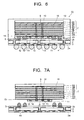
- FIG. 8A and FIG. 8B are cross-sectional views each illustrating a second manufacturing method of the semiconductor device illustrated in FIG. 6 .
- FIG. 9 is a cross-sectional view illustrating a semiconductor device according to a fifth embodiment.
- FIG. 10A and FIG. 10B are cross-sectional views each illustrating a first manufacturing method of the semiconductor device illustrated in FIG. 9 .
- FIG. 11A and FIG. 11B are cross-sectional views each illustrating a second manufacturing method of the semiconductor device illustrated in FIG. 9 .
- FIG. 12 is a cross-sectional view illustrating a semiconductor device according to a sixth embodiment.
- FIG. 13 is a cross-sectional view illustrating a semiconductor device according to a seventh embodiment.
- FIG. 14A to FIG. 14H are cross-sectional views each illustrating a manufacturing method of a semiconductor device according to an eighth embodiment.
- a semiconductor device including: an interposer substrate having a first surface provided with an external connection terminal and a second surface provided with an internal connection terminal; a chip stacked body, disposed on the second surface of the interposer substrate, having plural semiconductor chips sequentially stacked; and an interface chip mounted on an uppermost semiconductor chip in a stacking order of the plural semiconductor chips.
- the plural semiconductor chips are electrically connected via first through electrodes provided in the semiconductor chips excluding a lowermost semiconductor chip in the stacking order and a first bump electrode connecting the first through electrodes.
- the lowermost semiconductor chip is electrically connected to the interposer substrate via at least one semiconductor chip having the first through electrode.
- the interface chip is electrically connected to the uppermost semiconductor chip via a second bump electrode.
- the interface chip is electrically connected to the internal connection terminal via a rewiring layer formed on a surface of the uppermost semiconductor chip or a second through electrode provided in the interface chip.
- semiconductor devices in embodiments and manufacturing methods thereof will be explained with reference to the drawings.
- a semiconductor memory device using memory chips such as nonvolatile memories of NAND-type flash memories, or the like as semiconductor chips, but the semiconductor devices in the embodiments and the manufacturing methods thereof are not limited to it.
- FIG. 1 illustrates a semiconductor device according to a first embodiment.
- a semiconductor device 1 illustrated in FIG. 1 is a semiconductor memory device using memory chips as the semiconductor chips.
- the semiconductor device 1 includes an interposer substrate 2 .
- the interposer substrate 2 is formed by providing a wiring network 3 on a front surface or inside of an insulating resin substrate, for example, and concretely, a printed wiring substrate (a multilayer printed substrate or the like) using an insulating resin such as a glass-epoxy resin or a BT resin (Bismaleimide-Triazine resin) is applied.
- the interposer substrate 2 has a first surface 2 a to be a formation surface of external connection terminals and a second surface 2 b to be a disposition surface of a chip stacked body.
- connection terminals 4 are formed on the first surface 2 a of the interposer substrate 2 .
- the external connection terminals 4 are each formed of a projecting terminal made of solder ball, solder plating, Au plating, and the like.
- metal lands are provided as the external connection terminals 4 .
- internal connection terminals 5 are provided on the second surface 2 b of the interposer substrate 2 .
- the internal connection terminals 5 function as connection portions (connection pads) at the time of connecting the chip stacked body, and are electrically connected to the external connection terminals 4 via the wiring network 3 of the interposer substrate 2 .
- a chip stacked body 7 having plural memory chips 6 ( 6 A to 6 H) is disposed on the second surface 2 b of the interposer substrate 2 .
- the chip stacked body 7 is constituted in a manner that the plural memory chips 6 B to 6 H are sequentially stacked on the lowermost memory chip 6 A.
- the plural memory chips 6 A to 6 H have the same rectangular shape.
- the chip stacked body 7 is constituted by the eight memory chips 6 A to 6 H, but the number of the memory chips 6 is not limited to this.
- the number of the memory chips 6 is properly set according to a storage capacity of the single memory chip 6 , a storage capacity and use application of the semiconductor memory device 1 , and the like.
- lowermost memory chip and uppermost memory chip in the chip stacked body 7 are based on a stacking order of the plural memory chips 6 A to 6 H, and the lowermost memory chip and the uppermost memory chip do not necessarily agree with disposition positions on the interposer substrate 2 .
- the case of the memory chip of the certain number-th tier is also the same.
- the lowermost memory chip 6 A indicates the memory chip positioned at the lowermost level when the plural memory chips 6 A to 6 H are stacked.
- the uppermost memory chip 6 H indicates the memory chip positioned at the uppermost level when the plural memory chips 6 A to 6 H are stacked.
- the chip stacked body 7 is mounted on the second surface 2 b of the interposer substrate 2 by adhering a lower surface (a non-circuit surface) of the lowermost memory chip 6 A to the second surface 2 b of the interposer substrate 2 with an adhesive layer 8 .
- the lowermost memory chip 6 A in the stacking order of the chip stacked body 7 is only adhered to the second surface 2 b of the interposer substrate 2 with the adhesive layer 8 made of an insulating resin and the like, and is not directly electrically connected to wirings (the internal connection terminal 5 ) provided on the second surface 2 b of the interposer substrate 2 .
- the lowermost memory chip 6 A is electrically connected to the wirings of the interposer substrate 2 via the memory chips 6 B to 6 H.
- the chip stacked body 7 has the memory chips 6 adjacent to each other electrically connected via through electrodes (Through Silicon Via: TSV) 9 provided in the respective insides of the second memory chip 6 B to the uppermost memory chip 6 H and bump electrodes 10 connecting these through electrodes 9 .
- the memory chips 6 B to 6 H are sequentially stacked on the memory chip 6 A adhered to the interposer substrate 2 , for example.
- the lowermost memory chip 6 A is only adhered to the second surface 2 b of the interposer substrate 2 with the adhesive layer 8 , and is electrically connected only to the second memory chip 6 B. For this reason, the lowermost memory chip 6 A does not need to have the through electrode.
- the lowermost memory chip 6 A does not have the through electrode.
- FIG. 1 illustrates electrical connection structures between the memory chips 6 adjacent to each other in a simplified manner.
- a first electrode terminal formed on an upper surface (a circuit surface) of the memory chip 6 on the lower side to be electrically connected to the through electrodes 9 and second electrode terminals formed on a lower surface (a non-circuit surface) of the memory chip 6 on the upper side to be electrically connected to the through electrodes 9 are brought into contact with each other and are integrated by melting at least one electrode terminal of the first and second electrode terminals, and thereby the memory chips 6 adjacent to each other are electrically connected.
- the bump electrodes 10 illustrated in FIG. 1 each indicate a connection body of the first electrode terminal and the second electrode terminal.
- the memory chips 6 B to 6 H are sequentially stacked on the memory chip 6 A adhered to the interposer substrate 2 while the memory chips 6 adjacent to each other are electrically connected via the bump electrodes 10 each being the connection body of the first and second electrode terminals.
- solder material made of an Sn alloy in which Cu, Ag, Bi, In and so on are added to Sn and a metallic material such as Au, Cu, Ni, Sn, Pd, and Ag
- a solder material Pb-free solder
- an Sn—Cu alloy, an Sn—Ag alloy, an Sn—Ag—Cu alloy, and so on can be cited.
- the metallic material may be a stacked film of plural metal films such as Ni/Au or Ni/Pd/Au without being limited to a single layer film. Further, the metallic material may also be an alloy containing the metals as described above.
- a solder/solder, a metal/solder, a solder/metal, a metal/metal, and so on can be cited.
- shapes of the first and second electrode terminals a combination of projecting shapes with each other such as a hemispherical shape and a columnar shape, and a combination of a projecting shape and a flat shape such as a pad can be cited.
- At least one of the first and second electrode terminals is preferably made of the solder material.
- the first electrode terminals each made of the metallic material such as Ni/Au or Ni/Pd/Au on the upper surface (the circuit surface) of each of the memory chips 6 and to form the second electrode terminals each made of the solder material such as an Sn—Cu alloy, an Sn—Ag alloy, or an Sn—Ag—Cu alloy on the lower surface (the non-circuit surface) of each of the memory chips 6 .
- the first electrode terminal made of the metallic material preferably has a flat shape
- the second electrode terminal made of the solder material preferably has a projecting shape.
- the upper surfaces each having the flat first electrode terminals thereon are kept, and thereby the handleability of the memory chips 6 is improved, and this makes it possible to improve positioning accuracy between the memory chips 6 and connectivity by the bump electrodes 10 .
- the outer shapes of the memory chips 6 A to 6 H constituting the chip stacked body 7 are set to be same rectangular shape as described above.
- the memory chips 6 A to 6 H may also each have the same thickness, but the thickness of the lowermost memory chip 6 A is preferably made thicker than that of the other memory chips 6 B to 6 H.
- the thermal expansion coefficient of Si constituting the memory chip 6 A is 3 ppm/° C.
- the thermal expansion coefficient of a resin substrate used as the interposer substrate 2 is 10 ppm/° C. or more, so that the expansion at the time of the curing process of the adhesive layer 8 (at the time of a heating process) becomes larger in the interposer substrate 2 than in the memory chip 6 A. For this reason, by contraction in a cooling process after the curing process, in an adhered body of the interposer substrate 2 and the memory chip 6 A, warpage convex toward the upper surface side of the chip is likely to occur.
- the stacking of the memory chips 6 B to 6 H becomes difficult to be performed.
- an amount of the warpage of the lowermost memory chip 6 a after the adhesion is large with respect to the height of the bump electrode 10 , in stacking the memory chips 6 B to 6 H, the electrode terminal on the front surface of the chip on the lower side and the electrode terminal on the rear surface of the chip on the upper side do not come into contact with each other, and thus a connection failure is caused.
- connection is made under high temperature because the amount of warpage is reduced at the time of heating.
- the memory chips 6 are thereafter cooled to room temperature, the warpage occurs, and there is a risk that the connection by the bump electrodes is broken by the above warpage and chip cracking starting from connection portions occurs.
- the amount of warpage to occur relies on a property and a curing temperature of an adhesive, the thicknesses of the memory chip 6 and the interposer substrate 2 , and so on, but the most dominant factor of the warpage is the thickness of the memory chip (semiconductor chip) 6 .
- the thickness of the lowermost memory chip 6 A is thinner, the amount of warpage becomes larger.
- the thickness of the lowermost memory chip 6 A is preferably thicker than that of the other memory chips 6 B to 6 H. This makes it possible to improve a stacking yield of the memory chips 6 B to 6 H.
- the memory chips 6 B to 6 H excluding the lowermost memory chip 6 A are each preferably reduced in thickness in order to reduce the thickness of the chip stacked body 7 and further the thickness of the semiconductor memory device 1 .
- the memory chips 6 B to 6 H each having a thickness in a range of 20 to 40 ⁇ m are preferably used.
- the memory chip 6 A preferably has a thickness in a range of 100 to 300 ⁇ m. When the thickness of the memory chip 6 A is less than 100 ⁇ m, an effect of suppressing the warpage cannot be obtained sufficiently. When the thickness of the memory chip 6 A is increased too much, the thickness of the chip stacked body 7 is increased, and further the size of the semiconductor memory device 1 becomes too large.
- the thickness of the lowermost memory chip 6 A is preferably set to 300 ⁇ m or less. The lowermost memory chip 6 A does not need the through electrodes, so that it is possible to easily increase the chip thickness.
- a semiconductor chip in which a supporting plate having a thickness equivalent to the increased thickness of the memory chip 6 is adhered to its non-circuit surface with an adhesive, in place of using the thick memory chip 6 A.
- a memory chip whose thickness is reduced similarly to the memory chips 6 B to 6 H can be applied to the lowermost memory chip 6 A.
- the supporting plate for example, a Si plate or a metal plate having a physical property value equivalent to that of Si is applied.
- a metal plate having a thermal expansion coefficient equivalent to that of Si and having a large Young's modulus is preferably used.
- an Fe—Ni based alloy plate such as, for example, a 42 alloy is cited and is advantageous as compared with Si in terms of the cost.
- the supporting plate is preferably formed of a material having a large Young's modulus. As the Young's modulus is larger, a larger effect of reducing the warpage can be obtained with a thin plate thickness.
- the above-described manufacturing process of the chip stacked body 7 is effective not only in the case when the plural memory chips 6 are directly stacked on the interposer substrate 2 but also in the case when the plural memory chips 6 are temporarily adhered to a supporting substrate such as a glass substrate with an adhesive to be stacked.
- a supporting substrate such as a glass substrate with an adhesive to be stacked.
- the chip stacked body 7 separated from the supporting substrate is mounted on the interposer substrate 2 .
- the lowermost thick memory chip 6 A and the memory chip having the supporting plate adhered to the non-circuit surface act effectively.
- the chip stacked body 7 is manufactured on the supporting substrate made of a metal substrate, a Si substrate, or the like, and the chip stacked body 7 adhered to the supporting substrate is mounted on the interposer substrate 2 .
- the supporting substrate can not only become a base on which the plural memory chips 6 are stacked but also function as the supporting plate of suppressing the warpage of the memory chip 6 .
- the manufacturing process of the chip stacked body 7 using the supporting substrate will be described in detail later.
- an interface chip (IF chip) 11 provided with an interface (IF) circuit for performing data communications between the plural memory chips 6 A to 6 H constituting the chip stacked body 7 and an external device.
- the IF chip 11 is electrically connected to the chip stacked body 7 and has internal connection electrodes 12 performing data communications with the respective memory chips 6 A to 6 H.
- the internal connection electrodes 12 of the IF chip 11 are electrically connected to the through electrodes 9 of the uppermost memory chip 6 H via bump electrodes 13 .
- the IF chip 11 is flip-chip connected (FC connected) to the uppermost memory chip 6 H.
- the IF chip 11 has an external connection electrodes 14 performing data communications with an external device via the interposer substrate 2 .
- a rewiring layer 15 is formed in order to electrically connect the external connection electrodes 14 of the IF chip 11 and the internal connection terminals 5 of the interposer substrate 2 .
- One end portion of the rewiring layer 15 is electrically connected to the external connection electrode 14 of the IF chip 11 via a bump electrode 16 .
- the other end portion of the rewiring layer 15 and the internal connection terminal 5 of the interposer substrate 2 are electrically connected via a bonding wire (a metal wire such as an Au wire) 17 .
- the external connection electrode 14 of the IF chip 11 is electrically connected to the internal connection terminal 5 of the interposer substrate 2 via the bump electrode 16 , the rewiring layer 15 , and the bonding wire 17 .
- One end portion of the bonding wire 17 is connected to a bonding pad (not illustrated) which is disposed on the outer peripheral side of the surface of the uppermost memory chip 6 H and is electrically connected to the rewiring layer 15 .
- the rewiring layer 15 is formed so as to connect the bonding pad and a connection portion of the external connection electrode 14 .
- the bonding pad may also be formed on an end portion, of the rewiring layer 15 , positioned on the outer peripheral side of the chip.
- the semiconductor chip to be mounted on the chip stacked body 7 is not limited to the IF chip 11 having only the IF circuit mounted thereon.
- the IF chip 11 for performing data communications between the chip stacked body 7 and an external device may also be one on which a controller circuit is mounted in addition to the IF circuit.
- a mixed chip of the IF circuit and the controller circuit namely a chip combined with a controller and an IF may also be mounted.
- An underfill resin 18 is filled into a gap between each two of the memory chips 6 constituting the chip stacked body 7 and further a gap between the uppermost memory chip 6 H and the IF chip 11 .
- a sealing resin layer 19 made of an insulating resin such as an epoxy resin is formed by molding, for example, so as to seal the chip stacked body 7 and the IF chip 11 together with the bonding wire 17 .
- the semiconductor memory device (a stack semiconductor device/stack semiconductor package) 1 in the first embodiment is configured.
- the IF circuit is provided in a chip (IF chip 11 ) different from the memory chips 6 , and the chip is mounted on the chip stacked body 7 .
- the outer shapes of the plural memory chips 6 A to 6 H can be set to be the same, so that it is possible to miniaturize the chip stacked body 7 in which the plural memory chips 6 A to 6 H are stacked and further to reduce the package size of the semiconductor memory device 1 including the chip stacked body 7 , as compared with the case where the IF circuit is incorporated in a lowermost memory chip, for example.
- the memory chips 6 having the same structure except that the lowermost memory chip 6 A does not have the through electrode are used for the plural memory chips 6 A to 6 H, so that it becomes possible to achieve improvement of development efficiency, a reduction in manufacturing cost, and the like.
- the chip stacked body 7 is electrically connected to the interposer substrate 2 via the IF chip 11 .
- the chip stacked body 7 is only adhered to the second surface 2 b of the interposer substrate 2 , so that the cost required for mounting the chip stacked body 7 can be reduced.
- there is no need to form the through electrodes in the lowermost memory chip 6 A so that it is possible to easily increase the thickness of the lowermost memory chip 6 A.
- an effect of stress based on the difference in thermal expansion between the lowermost memory chip 6 A and the interposer substrate 2 and the warpage of the memory chip 6 A are suppressed.
- the IF chip 11 performing data communications between the chip stacked body 7 and an external device is electrically connected to the interposer substrate 2 via the rewiring layer 15 formed on the uppermost memory chip 6 H and the bonding wire 17 .
- a connection structure between the IF chip 11 and the interposer substrate 2 is simplified, so that it is possible to reduce the number of manufacturing processes and the manufacturing cost of the chip stacked body 7 containing the IF chip 11 , as compared with the case where the through electrodes for connecting the IF chip and the interposer substrate, and so on are provided in the memory chip. That is, it becomes possible to provide the miniaturized semiconductor memory device 1 excellent in reliability at low cost.
- the connection structure between the IF chip 11 and the interposer substrate 2 is simplified, thereby making it possible to achieve improvement of the speed of data communications between the chip stacked body 7 and an external device, and so on.
- the semiconductor memory device 1 in the first embodiment is manufactured in a manner that the underfill resin 18 is filled into a gap between each two of the plural memory chips 6 and then the rewiring layer 15 and the interposer substrate 2 are electrically connected by the bonding wire 17 .
- the underfill resin 18 is filled into the gap between of the plural memory chips 6 , there is a risk that the rewiring layer 15 and the internal connection terminal 5 are contaminated.
- the electrical connection by wire bonding cannot be performed.
- the rewiring layer 15 on the chip stacked body 7 and the interposer substrate 2 are electrically connected by the bonding wire 17 , and then the underfill resin 18 is filled into the chip stacked body 7 .
- the wire bonding is performed on the chip stacked body 7 in which the underfill resin 18 is not filled, so that there is a risk that cracking and the like occur in the memory chips 6 .
- spacers are disposed in a gap between each two of the memory chips 6 constituting the chip stacked body 7 . This makes it possible to soundly perform the wire bonding on the chip stacked body 7 in which the underfill resin 18 is not filled after the contamination of the rewiring layer 15 and the internal connection terminal 5 with the underfill resin 18 is prevented.
- FIG. 2 illustrates a semiconductor device (semiconductor memory device) 21 according to the second embodiment.
- the semiconductor memory device 21 according to the second embodiment basically has the same configuration as that of the semiconductor device 1 according to the first embodiment except that spacers 22 are disposed in a gap between each two of the memory chips 6 constituting the chip stacked body 7 and the underfill resin is filled after performing the wire bonding.
- the spacer 22 is preferably formed of an insulating resin such as an epoxy resin, a polyimide resin, an acrylic resin, a phenol resin, or a benzocyclobutene resin.
- the spacer 22 may also be formed of a resin having a photosensitivity and a thermosetting property.
- a thermosetting resin containing a photosensitive agent such as a photosensitive adhesive resin can be cited.
- the photosensitive and thermosetting resin is cured by irradiation of ultraviolet light at the formation stage of the spacers 22 , so that it is possible to make the spacers 22 function as a stopper keeping a gap between the memory chips 6 . Further, the resin is heated to be cured, and thereby the spacers 22 are adhered to the memory chips 6 , so that it is possible to increase adhesive strength between the memory chips 6 in the chip stacked body 7 in which the underfill resin is not filled. These make it possible to suppress occurrence of a short circuit caused by excessive crushing of the bump electrodes 10 and occurrence of a connection failure (open failure) of the bump electrodes 10 caused by the warpage of the memory chip 6 .
- the spacers 22 effectively function not only in the case when the wire bonding is performed and then the underfill resin 18 is filled, but also for the chip stacked body 7 in which the plural memory chips 6 are electrically connected by the through electrodes 9 and the bump electrodes 10 .
- the spacers 22 are disposed in a gap between each two of the memory chips 6 , and thereby when the memory chips 6 adjacent to each other are connected by the bump electrodes 10 , a gap between the memory chips 6 can be kept.
- the spacers 22 having adhesiveness it is possible to obtain a function of keeping a gap between each two of the memory chips 6 and an effect of improving adhesive strength between the memory chips 6 .
- the spacers 22 are preferably used also in the chip stacked body 7 in each of the other embodiments.
- FIG. 3A the plural memory chips 6 ( 6 A to 6 D) are stacked on the second surface 2 b of the interposer substrate 2 .
- the lowermost memory chip 6 A is adhered to the second surface 2 b of the interposer substrate 2 .
- first electrode terminals 23 are provided on the circuit surface of the memory chip 6 A.
- the second memory chip 6 B is stacked on the memory chip 6 A.
- second electrode terminals (solder bumps) 24 each made of the above-described solder material and the spacers 22 are provided.
- first electrode terminals 23 each made of the metallic material are provided.
- the memory chip 6 B after positioning of the second electrode terminals 24 on the first electrode terminals 23 on the memory chip 6 A is performed, is pressure-bonded to the memory chip 6 A while keeping a gap between the memory chips 6 A and 6 B with the spacers 22 .
- the third memory chip 6 C and the fourth memory chip 6 D are stacked.
- the IF chip 11 having electrode terminals 25 formed on its circuit surface is stacked on the memory chip 6 D.
- the electrode terminals 25 are each made of the solder material and are connected to the first electrode terminals 23 formed on the circuit surface of the memory chip 6 D of the fourth tier.
- the pressure-bonding temperature may be set to the connection temperature of the electrode terminals 23 and 24 ( 25 ) or higher, or may also be a temperature at which the electrode terminals 23 and 24 ( 25 ) are temporarily fixed. In the case when the electrode terminals 23 and 24 ( 25 ) are temporarily fixed, all the semiconductor chips containing the memory chips 6 and the IF chip 11 are stacked, and then are pressure-bonded or ref lowed in a reducing atmosphere at a temperature of the connection temperature of the electrode terminals 23 and 24 ( 25 ) or higher.
- the memory chips 6 A to 6 D are electrically and mechanically connected by the bump electrodes 10 (connection bodies each composed of the first electrode terminal 23 and the second electrode terminal 24 ) to manufacture the chip stacked body 7 , and on the chip stacked body 7 , the IF chip 11 is mounted.
- the IF chip 11 is electrically and mechanically connected to the chip stacked body 7 via the bump electrodes 13 (connection bodies each composed of the electrode terminal 23 and the electrode terminal 25 ).
- the spacers 22 are disposed in a gap between each two of the memory chips 6 A to 6 D constituting the chip stacked body 7 .
- the wire bonding is performed on the chip stacked body 7 .
- the bonding wires 17 are each connected to the bonding pad provided on the end portion of the rewiring layer 15 and the internal connection terminal 5 on the interposer substrate 2 .
- the spacers 22 as illustrated in FIG. 4 , are disposed so as to be positioned below the bonding pads provided on the end portions of the rewiring layers 15 .
- the underfill resin 18 is filled into a gap between each two of the memory chips 6 A to 6 D and a gap between the memory chip 6 D and the IF chip 11 .
- the underfill resin 18 is cured. By filling the underfill resin 18 after the wire bonding, the connection reliability by the bonding wires 17 can be maintained.
- the semiconductor memory device 1 in the first embodiment the plural memory chips 6 are stacked on the interposer substrate 2 , and the underfill resin 18 is filled on the interposer substrate 2 .
- the underfill resin 18 is filled into a gap between each two of the plural memory chips 6 , there is a risk that the internal connection terminal 5 on the interposer substrate 2 is contaminated with the underfill resin 18 . Further, there is a risk that due to the difference in thermal expansion coefficient between the memory chip 6 and the interposer substrate 2 , the warpage and the like occur in the memory chip 6 .
- the supporting substrate may be separated after the plural memory chips 6 are stacked, or the chip stacked body 7 having the supporting substrate may also be mounted on the interposer substrate 2 . In the third embodiment, the case where the chip stacked body 7 having the supporting substrate is mounted on the interposer substrate 2 will be explained.
- a supporting substrate 31 is prepared.
- the supporting substrate 31 has an outer shape larger than the memory chips 6 and smaller than the interposer substrate 2 .
- the supporting substrate 31 is preferably made of a metal plate having a physical property value equivalent to that of Si.
- As the metal plate an Fe—Ni based alloy plate is taken as an example.
- the supporting substrate 31 may also be a Si substrate, a glass substrate, or the like in place of the metal plate.
- the supporting substrate 31 has a chip mounting portion 31 a and a groove 31 b provided in the periphery of the chip mounting portion 31 a .
- the groove 31 b functions as a holding portion of the underfill resin.
- the chip mounting portion 31 a has a thickness based on the original thickness of the supporting substrate 31 , so that the plural memory chips 6 are stacked on the chip mounting portion 31 a excellent in flatness. Thus, it is possible to improve the connection reliability by the bump electrodes 10 . Further, the groove 31 b is provided in the periphery of the chip mounting portion 31 a , so that the underfill resin does not flow out to the outside of the supporting substrate 31 .
- the plural memory chips 6 ( 6 A to 6 H) and the IF chip 11 are stacked.
- the lowermost memory chip 6 A is adhered to the chip mounting portion 31 a of the supporting substrate 31 .
- the second memory chip 6 B to the eighth memory chip 6 H are sequentially stacked, and finally on the memory chip 6 H, the IF chip 11 is mounted.
- the stacking of the memory chips 6 A to 6 H and the mounting of the IF chip 11 are performed in the same manner as that in the second embodiment.
- the memory chip 6 A has the first electrode terminals provided on the circuit surface.
- the memory chips 6 B to 6 H each have the first electrode terminals provided on the circuit surface and the second electrode terminals provided on the non-circuit surface. On each of the non-circuit surfaces of the memory chips 6 B to 6 H, the spacers 22 are further provided.
- the first electrode terminals are each preferably made of the metallic material, and the second electrode terminals are each preferably made of the solder material.
- the memory chips 6 A to 6 H are stacked while, on the memory chips 6 adjacent to each other, the first electrode terminals and the second electrode terminals are connected. The gaps, each of which is between the memory chips 6 adjacent to each other, are kept by the spacers 22 . Finally, the IF chip 11 having the electrode terminals formed on its circuit surface is stacked on the memory chip 6 H. On the circuit surface of the uppermost memory chip 6 H, the rewiring layers 15 are formed. The electrode terminals of the IF chip 11 are each made of the solder material and are connected to electrode terminals provided on the rewiring layers 15 on the memory chip 6 H.
- the pressure-bonding temperature of the semiconductor chips may be set to the connection temperature of the electrode terminals or higher, or may also be a temperature at which the electrode terminals are temporarily fixed. In the case when the electrode terminals are temporarily fixed, all the semiconductor chips containing the memory chips 6 and the IF chip 11 are stacked, and then are pressure-bonded or reflowed in a reducing atmosphere at a temperature of the connection temperature of the electrode terminals or higher.
- the memory chips 6 A to 6 H are connected by the bump electrodes 10 to manufacture the chip stacked body 7 , and on the chip stacked body 7 , the IF chip 11 is mounted.
- the IF chip 11 is electrically and mechanically connected to the chip stacked body 7 via the bump electrodes 13 .
- the spacers 22 are disposed in a gap between each two of the memory chips 6 A to 6 H constituting the chip stacked body 7 .
- the underfill resin 18 is filled into a gap between each two of the memory chips 6 A to 6 H, and a gap between the memory chip 6 H and the IF chip 11 .
- the underfill resin 18 is cured.
- the groove 31 b is provided in the periphery of the chip mounting portion 31 a of the supporting substrate 31 , and the underfill resin 18 protruded from an outer peripheral of the chip stacked body 7 is held in the groove 31 b , and thus the underfill resin 18 does not flow out to the outside of the supporting substrate 31 .
- the chip stacked body 7 provided with the supporting substrate 31 and the IF chip 11 is mounted on the interposer substrate 2 .
- the chip stacked body 7 is mounted by adhering the supporting substrate 31 to the interposer substrate 2 via an adhesive layer 32 .
- the wire bonding is performed on the chip stacked body 7 mounted on the interposer substrate 2 .
- the bonding wires 17 are each connected to a bonding pad 33 electrically connected to the rewiring layer 15 and the internal connection terminal 5 on the interposer substrate 2 . As illustrated in FIG.
- the sealing resin layer 19 made of an insulating resin such as an epoxy resin is formed on the interposer substrate 2 so as to seal the chip stacked body 7 and the IF chip 11 together with the bonding wires 17 .
- a semiconductor memory device (a stack semiconductor device/stack semiconductor package) 34 in the third embodiment is manufactured.
- a semiconductor memory device 41 illustrated in FIG. 6 has a structure in which the IF chip 11 and the interposer substrate 2 are flip-chip connected (FC connected), in place of having the structure in which the IF chip 11 and the interposer substrate 2 are wire bonded in the first embodiment.
- the semiconductor memory device 41 similarly to the first embodiment, includes the chip stacked body 7 having the IF chip 11 mounted on the memory chip 6 H of the uppermost tier.
- the structure of the chip stacked body 7 , the connection structure between the chip stacked body 7 and the IF chip 11 , and the like are the same as those of the semiconductor memory device 1 in the first embodiment.
- the chip stacked body 7 is disposed so that the uppermost memory chip 6 H in the stacking order may be positioned on the second surface 2 b side of the interposer substrate 2 .
- the order of the plural memory chips 6 A to 6 H when the chip stacked body 7 is disposed on the interposer substrate 2 is the same as the order (the stacking order) when the plural memory chips 6 A to 6 H are stacked.
- the order of the plural memory chips 6 A to 6 H when the chip stacked body 7 is disposed on the interposer substrate 2 is reverse to the order of the plural memory chips 6 A to 6 H being stacked.
- the uppermost memory chip 6 H in the stacking order is disposed at the position closest to the interposer substrate 2 , and is positioned as a lowermost level on the interposer substrate 2 .
- the IF chip 11 is mounted similarly to the first embodiment.
- the IF chip 11 is disposed between the interposer substrate 2 and the chip stacked body 7 .
- the rewiring layers 15 are formed similarly to the first embodiment. One end portion of each of the rewiring layers 15 is electrically connected to the electrode 14 of the IF chip 11 via the bump electrode 16 . The other end of each of the rewiring layers 15 is electrically connected to the internal connection terminal 5 on the interposer substrate 2 via a bump electrode 42 .
- the bump electrode 42 for substrate connection has a size larger than that of the bump electrode 16 for chip connection. That is, the bump electrode 42 for substrate connection has a size large enough to be capable of securing a disposition space for the IF chip 11 . Concretely, the bump electrode 42 has a size (height) large enough to be capable of securing the thickness of the IF chip 11 and the gap between the IF chip 11 and the interposer substrate 2 .
- a recessed portion may also be formed in the front surface of the interposer substrate 2 in manner to correspond to the disposition position of the IF chip 11 .
- the rewiring layers 15 formed on the surface of the uppermost memory chip 6 H in the stacking order are connected to the interposer substrate 2 via the bump electrodes 42 .
- the electrodes themselves of the memory chip 6 H of the uppermost tier are connected to the IF chip 11 , so that the chip stacked body 7 is electrically connected to the interposer substrate 2 via the IF chip 11 .
- the underfill resin 18 is filled into a gap between each two of the memory chips 6 constituting the chip stacked body 7 and a gap between the memory chip 6 H of the uppermost tier and the IF chip 11 . Further, the underfill resin 18 is also filled into a gap between the chip stacked body 7 and the IF chip 11 and the interposer substrate 2 .
- the sealing resin layer 19 made of an insulating resin such as an epoxy resin is formed by molding, for example, so as to seal the chip stacked body 7 .
- the chip stacked body 7 having the IF chip 11 mounted thereon is manufactured on the supporting substrate.
- the chip stacked body 7 is manufactured in a state of being fixed to the supporting substrate temporarily. For example, stacking of up to the IF chip 11 is performed on the chip stacked body 7 , and then the chip stacked body 7 is reflowed in a reducing atmosphere, and thereby the memory chips 6 are connected and the memory chip 6 and the IF chip 11 are connected.
- the chip stacked body 7 is separated from the supporting substrate and then is mounted on the interposer substrate 2 .
- the interposer substrate 2 having electrode terminals (solder bumps) 44 to be the bump electrodes 42 formed on the internal connection terminals 5 is prepared.
- the chip stacked body 7 is disposed in a reversed state to the order of the memory chips 6 A to 6 H being stacked.
- the chip stacked body 7 is disposed so that the rewiring layers 15 formed on the front surface of the memory chip 6 H of the uppermost tier in the stacking order may be connected to the electrode terminals 44 .
- the electrode terminals 44 are connected to the rewiring layers 15 and thereby the bump electrodes 42 are formed.
- the bump electrodes 42 are formed by reflowing the electrode terminals (solder bumps) 44 pressure-bonded to the rewiring layers 15 in a reducing atmosphere, for example.
- an underfill resin 43 is filled into a gap between the chip stacked body 7 containing the IF chip 11 and the interposer substrate 2 and then is cured.
- the forming process of the bump electrodes 42 may also be performed in an insulating resin having a reducing action in place of the reflow process of the electrode terminals 44 in a reducing atmosphere.
- the interposer substrate 2 having the electrode terminals (solder bumps) 44 formed on the internal connection terminals 5 is prepared.
- an insulating resin paste 45 is applied.
- the chip stacked body 7 is disposed in a reversed state to the order of the memory chips 6 A to 6 H being stacked. Positioning is performed so that the rewiring layers 15 may be connected to the electrode terminals 44 , and then the chip stacked body 7 is pressed down against the interposer substrate 2 .
- the chip stacked body 7 in a state of being pressed down against the interposer substrate 2 , is heated to a temperature that is equal to or higher than the connection temperature of the electrode terminals (solder bumps) 44 and is equal to or higher than the curing temperature of the insulating resin paste 45 .
- a heating treatment in the same manner as the bump electrodes 42 that connect the rewiring layers 15 and the internal connection terminals 5 on the interposer substrate 2 being formed, an underfill resin 46 made of a cured product of the insulating resin paste 45 protecting the bump electrodes 42 and the like is formed.
- the IF chip 11 is mounted on the chip stacked body 7 , so that the outer shapes of the plural memory chips 6 A to 6 H can be set to be the same.
- the IF circuit is mounted on the memory chip of the lowermost tier, for example, it is possible to miniaturize the chip stacked body 7 in which the plural memory chips 6 A to 6 H are stacked and further to reduce the package size of the semiconductor memory device 41 including the chip stacked body 7 .
- the memory chips 6 having the same structure except that the lowermost memory chip 6 A does not have the through electrodes are used for the plural memory chips 6 A to 6 H, so that it becomes possible to achieve improvement of development efficiency, a reduction in manufacturing cost, and the like.
- the IF chip 11 is electrically connected to the interposer substrate 2 via the rewiring layers 15 formed on the uppermost memory chip 6 H and the bump electrodes 42 .
- connection structure between the IF chip 11 and the interposer substrate 2 is simplified, and thereby it is possible to reduce the number of manufacturing processes and the manufacturing cost of the chip stacked body 7 containing the IF chip 11 , and it becomes possible to achieve improvement of the speed of data communications between the chip stacked body 7 and an external device, and so on.
- a semiconductor memory device 51 illustrated in FIG. 9 includes the chip stacked body 7 stacked on the supporting substrate 31 and the IF chip 11 .
- the chip stacked body 7 including the supporting substrate 31 and the IF chip 11 is manufactured in the same manner as that in the third embodiment.
- the manufacturing process is as illustrated in FIG. 5A to FIG. 5F .
- the semiconductor memory device 51 has the same structure as that of the semiconductor memory device 41 according to the fourth embodiment except that the chip stacked body 7 having the supporting substrate 31 is flip-chip connected (FC connected) to the interposer substrate 2 .
- the chip stacked body 7 adhered to the supporting substrate 31 is disposed so that the uppermost memory chip 6 H in the stacking order may be positioned closest to the interposer substrate 2 .
- the supporting substrate 31 is disposed at the position farthest from the interposer substrate 2 .
- the IF chip 11 is disposed between the chip stacked body 7 and the interposer substrate 2 .
- the rewiring layers 15 formed on the front surface of the uppermost memory chip 6 H are electrically connected to the internal connection terminals 5 on the interposer substrate 2 via the bump electrodes 42 .
- the bump electrodes 42 for substrate connection each have a size larger than that of the bump electrode 16 for chip connection.
- the chip stacked body 7 having the IF chip 11 mounted thereon is manufactured on the supporting substrate 31 .
- the manufacturing process of the chip stacked body 7 and the mounting process of the IF chip 11 are as illustrated in FIG. 5A to FIG. 5F .
- the chip stacked body 7 is disposed in a reversed state to the order of the memory chips 6 A to 6 H being stacked.
- the rewiring layers 15 formed on the front surface of the uppermost memory chip 6 H are pressure-bonded to the electrode terminals (solder bumps) 44 .
- an adhesive layer 52 may also be formed on a portion, on the interposer substrate 2 , facing the IF chip 11 .
- the adhesive layer 52 is to increase the adhesive strength between the chip stacked body 7 and the interposer substrate 2 that are not resin-sealed yet. Thereby, handleability of a structure that is not resin-sealed yet is improved. Further, a gap between the interposer substrate 2 and the IF chip 11 is filled with the adhesive layer 52 , and thereby it is possible to suppress occurrence of pores caused after the underfill resin 43 is filled, and the like.
- an adhesive containing metal particles such as Al particles may also be used.
- the electrode terminals (solder bumps) 44 pressure-bonded to the rewiring layers 15 are reflowed in a reducing atmosphere, and then the underfill resin 43 is filled into a gap between the chip stacked body 7 and the interposer substrate 2 and is cured.
- the forming process of the bump electrodes 42 may also be performed in an insulating resin having a reducing action similarly to the fourth embodiment.
- the insulating resin paste 45 is applied on the interposer substrate 2 having the electrode terminals (solder bumps) 44 formed on the internal connection terminals 5 .
- Positioning is performed so that the rewiring layers 15 may be connected to the electrode terminals 44 , and then the chip stacked body 7 is pressed down against the interposer substrate 2 .
- the chip stacked body 7 in a state of being pressed down against the interposer substrate 2 , is heated to a temperature that is equal to or higher than the connection temperature of the electrode terminals (solder bumps) 44 and is equal to or higher than the curing temperature of the insulating resin paste 45 .
- the underfill resin 46 made of a cured product of the insulating resin paste 45 protecting the bump electrodes 42 and the like is formed.
- a semiconductor memory device 61 illustrated in FIG. 12 has a structure in which the bonding wire 17 is directly connected to the IF chip 11 , in place of having the structure in which the bonding wire 17 is connected to the rewiring layer 15 in the first embodiment.
- the IF chip 11 has through electrodes 62 .
- the bonding wire 17 electrically connecting the IF chip 11 and the interposer substrate 2 may be directly connected to a bonding pad provided on the through electrode 62 of the IF chip 11 , or it may also be configured that depending on the formation position of the through electrodes 62 , the rewiring layer is formed on the front surface of the IF chip 11 , and the bonding wire 17 is connected to a bonding pad provided on an end portion of the rewiring layer.
- the configuration other than them is the same as that in the first embodiment.
- the package size can be reduced similarly to the first embodiment. Further, it becomes possible to achieve improvement of development efficiency of the memory chips 6 , a reduction in manufacturing cost, a reduction in mounting cost of the chip stacked body 7 , and the like. When the chip stacked body 7 is adhered to the interposer substrate 2 , it becomes possible to increase the electrical connection reliability between the memory chips 6 .
- connection structure between the IF chip 11 and the interposer substrate 2 is simplified, and thereby it is possible to reduce the number of manufacturing processes and the manufacturing cost of the chip stacked body 7 containing the IF chip 11 , and further it becomes possible to achieve improvement of the speed of data communications between the chip stacked body 7 and an external device, and so on.
- a semiconductor memory device 71 illustrated in FIG. 13 has a structure in which the bump electrodes are directly formed on the IF chip 11 , in place of having the structure in which the bump electrodes 42 are formed on the rewiring layers 15 in the fourth embodiment.
- the IF chip 11 has through electrodes 72 .
- the through electrodes 72 in the IF chip 11 are electrically connected to the internal connection terminals 5 on the interposer substrate 2 via bump electrodes 73 .
- Spacers 74 are interposed between the chip stacked body 7 and the interposer substrate 2 . The configuration other than them is the same as that of the fourth embodiment.
- the package size can be reduced. Further, it becomes possible to achieve improvement of development efficiency of the memory chips 6 , a reduction in manufacturing cost, and the like.
- the connection structure between the IF chip 11 and the interposer substrate 2 is simplified, and thereby it is possible to reduce the number of manufacturing processes and the manufacturing cost of the chip stacked body 7 containing the IF chip 11 , and further it becomes possible to achieve improvement of the speed of data communications between the chip stacked body 7 and an external device, and so on.
- the manufacturing process of the semiconductor device (the semiconductor memory device) according to the eighth embodiment is characterized in that a semiconductor wafer to be the lowermost memory chip is used as the supporting substrate and the chip stacked body is manufactured.
- a semiconductor wafer 81 is prepared.
- the semiconductor wafer 81 has plural chip areas X to be semiconductor chips after separation.
- the semiconductor chips based on the plural chip areas X each correspond to the lowermost memory chip of the chip stacked body.
- Dicing areas D are provided in gaps, each of which is between the plural chip areas X.
- circuit surfaces 81 a of the plural chip areas X semiconductor element portions each having a semiconductor circuit, a wiring layer, and so on, (which are not illustrated) are formed.
- electrode terminals 82 to be the bump electrodes are formed on each of the chip areas X.
- the chip areas X of the semiconductor wafer 81 each correspond to the lowermost memory chip, and thus each do not have the through electrodes formed therein.
- grooves 83 are formed in the semiconductor wafer 81 from the circuit surface 81 a side.
- the grooves 83 are each formed by cutting the dicing area D with a blade, for example.
- the depth of each of the grooves 83 is set to be shallower than the thickness of the semiconductor wafer 81 and deeper than the thickness of the memory chip at the time of completion.
- the grooves in a half-cut state (dicing grooves) 83 are formed.
- the dicing grooves 83 may also be formed by etching, or the like.
- the dicing grooves 83 each having such a depth are formed in the semiconductor wafer 81 , and thereby the plural chip areas X are divided in a state where the plural chip areas X each correspond to the thickness of the completed semiconductor chip.
- semiconductor chips 84 are stacked on the respective chip areas X of the semiconductor wafer 81 having the dicing grooves 83 in a half-cut state formed therein.
- the semiconductor chips 84 similarly to the memory chips 6 in each of the above-described embodiments, each have through electrodes 85 and electrode terminals to be bump electrodes 86 .
- the semiconductor chips 84 to be the memory chip of the second tier are each stacked while the electrode terminals are connected. The same stacking process is performed according to the number of the chips to be stacked, and thereby plural chip stacked bodies 87 are formed.
- FIG. 14A to FIG. 14H each illustrate a state where on the respective chip areas X, the seven semiconductor chips 84 are stacked, and the chip stacked bodies 87 each in which the eight semiconductor chips to which the semiconductor chip based on the chip area X is finally added are stacked are manufactured.
- the number of the semiconductor chips 84 to be stacked is not limited to this.
- the number of the semiconductor chips 84 to be stacked is properly set according to a storage capacity of the memory chip based on the semiconductor chips 84 and the like, a storage capacity according to the chip stacked body 87 containing the chip area X, use application of the semiconductor memory device including the chip stacked body 87 , and the like.
- the semiconductor chips 84 having the same shape as that of the chip area X are stacked, so that spaces 88 corresponding to spaces above the dicing grooves 83 are generated in gaps, each of which is between the chip stacked bodies 87 .
- spaces 88 are utilized.
- the space 88 between the chip stacked bodies 87 has a shape extending upward from the dicing groove 83 and thus is effective as a space used for filling the underfill resin into gaps in the chip stacked body 87 in which the semiconductor chips 84 are stacked in multiple.
- an underfill resin 89 is introduced into the spaces 88 that are positioned above the dicing grooves 83 and each are between the plural chip stacked bodies 87 , and thereby the underfill resin 89 is filled in the gaps in the chip stacked bodies 87 . Thereafter, the underfill resin 89 is cured, and thereby the underfill resins 89 filled into the gaps in the chip stacked bodies 87 , including the underfill resins 89 in the spaces 88 , are cured.
- the underfill resin 89 is introduced into the groove-shaped spaces 88 , each of which is between the plural chip stacked bodies 87 , and thereby it becomes possible to finely fill the underfill resin 89 into the gaps in the chip stacked bodies 87 in which the semiconductor chips 84 (containing the chip area X) are stacked in multiple tiers.
- a protection tape 90 is stuck to the top of the chip stacked bodies 87 , and then a non-circuit surface (a rear surface) 81 b of the semiconductor wafer 81 is grinded.
- the protection tape 90 is to protect circuit surfaces of the uppermost semiconductor chips 84 of the chip stacked bodies 87 when the non-circuit surface 81 b of the semiconductor wafer 81 is grinded and to maintain the shape of the semiconductor wafer 81 after the chip areas X are separated.
- various types of resin tapes, and the like are used as the protection tape 90 .
- the non-circuit surface 81 b of the semiconductor wafer 81 is mechanically grinded by using, for example, a wrapping plate, and subsequently polished (for example, dry-polished) by using a polishing plate.
- the grinding and polishing process of the non-circuit surface 81 b of the semiconductor wafer 81 is performed so as to reach the dicing grooves 83 . Thereby, the semiconductor wafer 81 is divided into the respective chip areas X to be separated from each other.
- the non-circuit surface (the rear surface) 81 b of the semiconductor wafer 81 By grinding the non-circuit surface (the rear surface) 81 b of the semiconductor wafer 81 , the plural chip areas X are separated from each other. Thereby, the chip stacked bodies 87 each having a semiconductor chip 91 as the lowermost memory chip are manufactured.
- the overall shape of the semiconductor wafer 81 is kept by the underfill resins 89 introduced into the spaces 88 , each of which is between the chip stacked bodies 87 .
- a dicing tape 92 is stuck, and then the protection tape 90 is peeled off.
- the underfill resins 89 existing in the spaces 88 are diced, and thereby the plural chip stacked bodies 87 are separated into individual bodies respectively.
- the plural chip stacked bodies 87 which are separated into individual bodies, are transferred to a pickup process being the subsequent process.
- the dicing tape 92 is stuck to the lowermost surface of each of the chip stacked bodies 87 , and thus the plural chip stacked bodies 87 are transferred to the pickup process in a state of being stuck to the dicing tape 92 .
- Each of the plural chip stacked bodies 87 transferred to the pickup process is sequentially picked up to be mounted on an interposer substrate 93 as illustrated in FIG. 14H .
- FIG. 14H illustrates the same mounted structure of the chip stacked body 87 as that in the first embodiment.
- the IF chip is mounted, of which the illustration is omitted in FIG. 14A to FIG. 14H .
- the IF chip is mounted on the chip stacked body 87 , and then the mounting process of the chip stacked body 87 on the interposer substrate 93 is performed.
- the lowermost semiconductor chip 91 of the chip stacked body 87 is not directly electrically connected to the interposer substrate 93 similarly to the first embodiment.
- the thickness of the semiconductor chip 91 is preferably thicker than that of the other semiconductor chips 84 . Thereby, it is suppressed that stress generated in an adhering process (the heating process) based on the difference in thermal expansion coefficient between the semiconductor chip 91 and the interposer substrate 93 adversely affects the bump electrodes and the like. Thus, it becomes possible to suppress occurrence of a connection failure caused by occurrence of cracking in and around the bump electrodes.
- the IF chip whose illustration is omitted, or the uppermost semiconductor chip 84 of the chip stacked body 87 and the internal connection terminal on the interposer substrate 93 are electrically connected by the bonding wire and then the chip stacked body 87 is sealed by the sealing resin layer, and thereby the semiconductor device such as the semiconductor memory device is manufactured.
- a circuit substrate on which the chip stacked body 87 is mounted may also be a lead frame or the like, in place of the interposer substrate 93 . In the case when the same mounting structure of the chip stacked body 87 as that of the second embodiment is applied, the IF chip is mounted on the chip stacked body 87 and then the mounting process of the chip stacked body 87 on the interposer substrate 93 is performed.
Applications Claiming Priority (4)
| Application Number | Priority Date | Filing Date | Title |
|---|---|---|---|
| JP2011-206869 | 2011-09-22 | ||
| JP2011206869 | 2011-09-22 | ||
| JP2012-200287 | 2012-09-12 | ||
| JP2012200287A JP5936968B2 (ja) | 2011-09-22 | 2012-09-12 | 半導体装置とその製造方法 |
Publications (2)
| Publication Number | Publication Date |
|---|---|
| US20130075895A1 US20130075895A1 (en) | 2013-03-28 |
| US8941246B2 true US8941246B2 (en) | 2015-01-27 |
Family
ID=47910372
Family Applications (1)
| Application Number | Title | Priority Date | Filing Date |
|---|---|---|---|
| US13/623,249 Active 2033-04-26 US8941246B2 (en) | 2011-09-22 | 2012-09-20 | Semiconductor device and manufacturing method thereof |
Country Status (4)
| Country | Link |
|---|---|
| US (1) | US8941246B2 (ja) |
| JP (1) | JP5936968B2 (ja) |
| CN (1) | CN103022021B (ja) |
| TW (1) | TWI483376B (ja) |
Cited By (12)
| Publication number | Priority date | Publication date | Assignee | Title |
|---|---|---|---|---|
| US9653132B2 (en) | 2015-06-03 | 2017-05-16 | Samsung Electronics Co., Ltd. | Semiconductor packages usable with semiconductor chips having different pad arrangements and electronic devices having the same |
| US9741695B2 (en) * | 2016-01-13 | 2017-08-22 | Globalfoundries Inc. | Three-dimensional hybrid packaging with through-silicon-vias and tape-automated-bonding |
| US10062627B2 (en) | 2016-03-17 | 2018-08-28 | Toshiba Memory Corporation | Semiconductor device |
| US10128153B2 (en) | 2015-06-15 | 2018-11-13 | Kabushiki Kaisha Toshiba | Method of fabricating a semiconductor device and the semiconductor device |
| US10186487B2 (en) | 2017-03-22 | 2019-01-22 | Toshiba Memory Corporation | Semiconductor device |
| US10187979B2 (en) * | 2016-12-28 | 2019-01-22 | Shinko Electric Industries Co., Ltd. | Wiring substrate and electronic component device |
| US10431547B2 (en) | 2017-07-05 | 2019-10-01 | Samsung Electronics Co., Ltd. | Semiconductor package |
| US10593649B2 (en) | 2018-03-20 | 2020-03-17 | Toshiba Memory Corporation | Semiconductor device |
| US10748871B2 (en) | 2018-03-26 | 2020-08-18 | Samsung Electronics Co., Ltd. | Semiconductor chip and semiconductor package including the same |
| US10943844B2 (en) | 2018-06-21 | 2021-03-09 | Toshiba Memory Corporation | Semiconductor device including multiple chips |
| US11502057B2 (en) | 2020-02-17 | 2022-11-15 | Kioxia Corporation | Semiconductor device and manufacturing method thereof |
| US11894346B2 (en) | 2016-02-22 | 2024-02-06 | Samsung Electronics Co., Ltd. | Semiconductor package having a high reliability |
Families Citing this family (25)
| Publication number | Priority date | Publication date | Assignee | Title |
|---|---|---|---|---|
| US9000599B2 (en) * | 2013-05-13 | 2015-04-07 | Intel Corporation | Multichip integration with through silicon via (TSV) die embedded in package |
| KR102041639B1 (ko) * | 2013-07-08 | 2019-11-07 | 삼성전기주식회사 | 고주파 모듈 |
| JP2015056563A (ja) * | 2013-09-12 | 2015-03-23 | 株式会社東芝 | 半導体装置およびその製造方法 |
| JP2015177007A (ja) * | 2014-03-14 | 2015-10-05 | 株式会社東芝 | 半導体装置の製造方法及び半導体装置 |
| JP2015177062A (ja) * | 2014-03-14 | 2015-10-05 | 株式会社東芝 | 半導体装置の製造方法および半導体装置 |
| US9786643B2 (en) | 2014-07-08 | 2017-10-10 | Micron Technology, Inc. | Semiconductor devices comprising protected side surfaces and related methods |
| DE102014112430A1 (de) | 2014-08-29 | 2016-03-03 | Ev Group E. Thallner Gmbh | Verfahren zur Herstellung eines leitenden Mehrfachsubstratstapels |
| JP6276151B2 (ja) | 2014-09-17 | 2018-02-07 | 東芝メモリ株式会社 | 半導体装置 |
| JP6212011B2 (ja) * | 2014-09-17 | 2017-10-11 | 東芝メモリ株式会社 | 半導体製造装置 |
| JP6747299B2 (ja) * | 2014-12-18 | 2020-08-26 | ソニー株式会社 | 半導体装置、製造方法、電子機器 |
| JP6495692B2 (ja) * | 2015-03-11 | 2019-04-03 | 東芝メモリ株式会社 | 半導体装置及びその製造方法 |
| JP2016225484A (ja) * | 2015-06-01 | 2016-12-28 | 株式会社東芝 | 半導体装置および半導体装置の製造方法 |
| US11081451B2 (en) * | 2017-03-10 | 2021-08-03 | Intel Corporation | Die stack with reduced warpage |
| JP7304335B2 (ja) | 2017-08-21 | 2023-07-06 | 長江存儲科技有限責任公司 | Nandメモリデバイスおよびnandメモリデバイスを形成するための方法 |
| US10700028B2 (en) | 2018-02-09 | 2020-06-30 | Sandisk Technologies Llc | Vertical chip interposer and method of making a chip assembly containing the vertical chip interposer |
| KR102506698B1 (ko) * | 2018-02-19 | 2023-03-07 | 에스케이하이닉스 주식회사 | 보강용 탑 다이를 포함하는 반도체 패키지 제조 방법 |
| US11471993B2 (en) | 2018-03-09 | 2022-10-18 | Hoya Corporation | Spacer, laminate of substrates, method for manufacturing substrate, and method for manufacturing substrate for magnetic disk |
| CN110660805B (zh) * | 2018-06-28 | 2023-06-20 | 西部数据技术公司 | 包含分支存储器裸芯模块的堆叠半导体装置 |
| KR102514903B1 (ko) | 2018-06-29 | 2023-03-27 | 양쯔 메모리 테크놀로지스 씨오., 엘티디. | 인터포저를 이용하여 장치 칩이 적층된 3차원 메모리 장치 |
| KR102551751B1 (ko) * | 2018-11-06 | 2023-07-05 | 삼성전자주식회사 | 반도체 패키지 |
| JP6689420B2 (ja) * | 2019-01-17 | 2020-04-28 | キオクシア株式会社 | 半導体装置および半導体装置の製造方法 |
| US10879260B2 (en) | 2019-02-28 | 2020-12-29 | Sandisk Technologies Llc | Bonded assembly of a support die and plural memory dies containing laterally shifted vertical interconnections and methods for making the same |
| US10923438B2 (en) | 2019-04-26 | 2021-02-16 | Taiwan Semiconductor Manufacturing Co., Ltd. | Package structure and method for forming the same |
| JP2021048195A (ja) * | 2019-09-17 | 2021-03-25 | キオクシア株式会社 | 半導体装置及び半導体装置の製造方法 |
| CN117133727A (zh) * | 2023-08-29 | 2023-11-28 | 江苏柒捌玖电子科技有限公司 | 一种三维堆叠封装结构及其封装方法 |
Citations (5)
| Publication number | Priority date | Publication date | Assignee | Title |
|---|---|---|---|---|
| JP2006301863A (ja) | 2005-04-19 | 2006-11-02 | Elpida Memory Inc | メモリモジュール |
| JP2007012848A (ja) | 2005-06-30 | 2007-01-18 | Elpida Memory Inc | 半導体記憶装置及びその製造方法 |
| US7531905B2 (en) * | 2006-01-20 | 2009-05-12 | Elpida Memory, Inc. | Stacked semiconductor device |
| JP2010287852A (ja) | 2009-06-15 | 2010-12-24 | Elpida Memory Inc | 半導体装置及びその製造方法 |
| US20110141789A1 (en) * | 2003-04-21 | 2011-06-16 | Elpida Memory, Inc. | Memory module and memory system |
Family Cites Families (13)
| Publication number | Priority date | Publication date | Assignee | Title |
|---|---|---|---|---|
| JP2997231B2 (ja) * | 1997-09-12 | 2000-01-11 | 富士通株式会社 | マルチ半導体ベアチップ実装モジュールの製造方法 |
| JP4205613B2 (ja) * | 2004-03-01 | 2009-01-07 | エルピーダメモリ株式会社 | 半導体装置 |
| JP4191167B2 (ja) * | 2005-05-16 | 2008-12-03 | エルピーダメモリ株式会社 | メモリモジュールの製造方法 |
| JP2007036104A (ja) * | 2005-07-29 | 2007-02-08 | Nec Electronics Corp | 半導体装置およびその製造方法 |
| JP4910512B2 (ja) * | 2006-06-30 | 2012-04-04 | 富士通セミコンダクター株式会社 | 半導体装置および半導体装置の製造方法 |
| TWI349318B (en) * | 2007-04-11 | 2011-09-21 | Siliconware Precision Industries Co Ltd | Stackable semiconductor device and manufacturing method thereof |
| JP2008294367A (ja) * | 2007-05-28 | 2008-12-04 | Nec Electronics Corp | 半導体装置およびその製造方法 |
| TWI355731B (en) * | 2008-02-26 | 2012-01-01 | Powertech Technology Inc | Chips-between-substrates semiconductor package and |
| JP2010107388A (ja) * | 2008-10-30 | 2010-05-13 | Denso Corp | マルチチップパッケージ |
| JP2010161102A (ja) * | 2009-01-06 | 2010-07-22 | Elpida Memory Inc | 半導体装置 |
| TWI401785B (zh) * | 2009-03-27 | 2013-07-11 | Chipmos Technologies Inc | 多晶片堆疊封裝 |
| JP5543125B2 (ja) * | 2009-04-08 | 2014-07-09 | ピーエスフォー ルクスコ エスエイアールエル | 半導体装置および半導体装置の製造方法 |
| JP5709218B2 (ja) * | 2009-11-27 | 2015-04-30 | 日本電気株式会社 | 半導体装置、3次元実装型半導体装置、半導体モジュール、電子機器、及びその製造方法 |
-
2012
- 2012-09-12 JP JP2012200287A patent/JP5936968B2/ja active Active
- 2012-09-17 TW TW101134048A patent/TWI483376B/zh active
- 2012-09-19 CN CN201210350172.2A patent/CN103022021B/zh active Active
- 2012-09-20 US US13/623,249 patent/US8941246B2/en active Active
Patent Citations (10)
| Publication number | Priority date | Publication date | Assignee | Title |
|---|---|---|---|---|
| US20110141789A1 (en) * | 2003-04-21 | 2011-06-16 | Elpida Memory, Inc. | Memory module and memory system |
| US8238134B2 (en) * | 2003-04-21 | 2012-08-07 | Elpida Memory, Inc. | Memory module and memory system |
| JP2006301863A (ja) | 2005-04-19 | 2006-11-02 | Elpida Memory Inc | メモリモジュール |
| US7564127B2 (en) | 2005-04-19 | 2009-07-21 | Elpida Memory, Inc. | Memory module that is capable of controlling input/output in accordance with type of memory chip |
| JP2007012848A (ja) | 2005-06-30 | 2007-01-18 | Elpida Memory Inc | 半導体記憶装置及びその製造方法 |
| US7576433B2 (en) | 2005-06-30 | 2009-08-18 | Elpida Memory, Inc. | Semiconductor memory device and manufacturing method thereof |
| US7893540B2 (en) | 2005-06-30 | 2011-02-22 | Elpida Memory, Inc. | Semiconductor memory device and manufacturing method thereof |
| US20110104852A1 (en) | 2005-06-30 | 2011-05-05 | Elpida Memory, Inc. | Semiconductor memory device and manufacturing method thereof |
| US7531905B2 (en) * | 2006-01-20 | 2009-05-12 | Elpida Memory, Inc. | Stacked semiconductor device |
| JP2010287852A (ja) | 2009-06-15 | 2010-12-24 | Elpida Memory Inc | 半導体装置及びその製造方法 |
Cited By (16)
| Publication number | Priority date | Publication date | Assignee | Title |
|---|---|---|---|---|
| US9653132B2 (en) | 2015-06-03 | 2017-05-16 | Samsung Electronics Co., Ltd. | Semiconductor packages usable with semiconductor chips having different pad arrangements and electronic devices having the same |
| US10128153B2 (en) | 2015-06-15 | 2018-11-13 | Kabushiki Kaisha Toshiba | Method of fabricating a semiconductor device and the semiconductor device |
| US9741695B2 (en) * | 2016-01-13 | 2017-08-22 | Globalfoundries Inc. | Three-dimensional hybrid packaging with through-silicon-vias and tape-automated-bonding |
| US20170271309A1 (en) * | 2016-01-13 | 2017-09-21 | Globalfoundries Inc. | Three-dimensional hybrid packaging with through-silicon-vias and tape-automated-bonding |
| US9972606B2 (en) * | 2016-01-13 | 2018-05-15 | Globalfoundries Inc. | Three-dimensional hybrid packaging with through-silicon-vias and tape-automated-bonding |
| US11894346B2 (en) | 2016-02-22 | 2024-02-06 | Samsung Electronics Co., Ltd. | Semiconductor package having a high reliability |
| US10062627B2 (en) | 2016-03-17 | 2018-08-28 | Toshiba Memory Corporation | Semiconductor device |
| US10187979B2 (en) * | 2016-12-28 | 2019-01-22 | Shinko Electric Industries Co., Ltd. | Wiring substrate and electronic component device |
| US10186487B2 (en) | 2017-03-22 | 2019-01-22 | Toshiba Memory Corporation | Semiconductor device |
| US10431547B2 (en) | 2017-07-05 | 2019-10-01 | Samsung Electronics Co., Ltd. | Semiconductor package |
| US11462479B2 (en) | 2017-07-05 | 2022-10-04 | Samsung Electronics Co., Ltd. | Semiconductor package |
| TWI695484B (zh) * | 2018-03-20 | 2020-06-01 | 日商東芝記憶體股份有限公司 | 半導體裝置 |
| US10593649B2 (en) | 2018-03-20 | 2020-03-17 | Toshiba Memory Corporation | Semiconductor device |
| US10748871B2 (en) | 2018-03-26 | 2020-08-18 | Samsung Electronics Co., Ltd. | Semiconductor chip and semiconductor package including the same |
| US10943844B2 (en) | 2018-06-21 | 2021-03-09 | Toshiba Memory Corporation | Semiconductor device including multiple chips |
| US11502057B2 (en) | 2020-02-17 | 2022-11-15 | Kioxia Corporation | Semiconductor device and manufacturing method thereof |
Also Published As
| Publication number | Publication date |
|---|---|
| JP5936968B2 (ja) | 2016-06-22 |
| JP2013080912A (ja) | 2013-05-02 |
| CN103022021A (zh) | 2013-04-03 |
| TWI483376B (zh) | 2015-05-01 |
| US20130075895A1 (en) | 2013-03-28 |
| CN103022021B (zh) | 2016-05-11 |
| TW201316486A (zh) | 2013-04-16 |
Similar Documents
| Publication | Publication Date | Title |
|---|---|---|
| US8941246B2 (en) | Semiconductor device and manufacturing method thereof | |
| US10128211B2 (en) | Thin fan-out multi-chip stacked package structure and manufacturing method thereof | |
| US8786102B2 (en) | Semiconductor device and method of manufacturing the same | |
| JP5814859B2 (ja) | 半導体装置とその製造方法 | |
| JP5847749B2 (ja) | 積層型半導体装置の製造方法 | |
| US9312240B2 (en) | Semiconductor packages and methods of packaging semiconductor devices | |
| TWI620291B (zh) | Semiconductor device | |
| US10276545B1 (en) | Semiconductor package and manufacturing method thereof | |
| US9570414B2 (en) | Semiconductor device and method of manufacturing the semiconductor device | |
| US20160079222A1 (en) | Semiconductor device having terminals formed on a chip package including a plurality of semiconductor chips and manufacturing method thereof | |
| TW201921625A (zh) | 具有橫向偏移堆疊之半導體晶粒之半導體裝置 | |
| US20070231966A1 (en) | Semiconductor device fabricating method | |
| TWI724744B (zh) | 半導體裝置及半導體裝置之製造方法 | |
| US7498199B2 (en) | Method for fabricating semiconductor package | |
| JP2015177062A (ja) | 半導体装置の製造方法および半導体装置 | |
| JP2015177061A (ja) | 半導体装置の製造方法および半導体装置 | |
| JP6100489B2 (ja) | 半導体装置の製造方法 | |
| TWI612589B (zh) | 半導體裝置及其製造方法 | |
| JP4496241B2 (ja) | 半導体素子とそれを用いた半導体パッケージ | |
| US9136219B2 (en) | Expanded semiconductor chip and semiconductor device | |
| JP2012009713A (ja) | 半導体パッケージおよび半導体パッケージの製造方法 | |
| TWI688067B (zh) | 半導體裝置及其製造方法 | |
| US10854576B2 (en) | Semiconductor device and manufacturing method thereof | |
| JP6486855B2 (ja) | 半導体装置および半導体装置の製造方法 | |
| JP2015222837A (ja) | 半導体装置 |
Legal Events
| Date | Code | Title | Description |
|---|---|---|---|
| AS | Assignment |
Owner name: KABUSHIKI KAISHA TOSHIBA, JAPAN Free format text: ASSIGNMENT OF ASSIGNORS INTEREST;ASSIGNORS:MIURA, MASAYUKI;KAMOTO, TAKU;SATO, TAKAO;SIGNING DATES FROM 20120928 TO 20121009;REEL/FRAME:029463/0343 |
|
| STCF | Information on status: patent grant |
Free format text: PATENTED CASE |
|
| AS | Assignment |
Owner name: TOSHIBA MEMORY CORPORATION, JAPAN Free format text: ASSIGNMENT OF ASSIGNORS INTEREST;ASSIGNOR:KABUSHIKI KAISHA TOSHIBA;REEL/FRAME:043709/0035 Effective date: 20170706 |
|
| MAFP | Maintenance fee payment |
Free format text: PAYMENT OF MAINTENANCE FEE, 4TH YEAR, LARGE ENTITY (ORIGINAL EVENT CODE: M1551) Year of fee payment: 4 |
|
| AS | Assignment |
Owner name: K.K. PANGEA, JAPAN Free format text: MERGER;ASSIGNOR:TOSHIBA MEMORY CORPORATION;REEL/FRAME:055659/0471 Effective date: 20180801 Owner name: TOSHIBA MEMORY CORPORATION, JAPAN Free format text: CHANGE OF NAME AND ADDRESS;ASSIGNOR:K.K. PANGEA;REEL/FRAME:055669/0401 Effective date: 20180801 Owner name: KIOXIA CORPORATION, JAPAN Free format text: CHANGE OF NAME AND ADDRESS;ASSIGNOR:TOSHIBA MEMORY CORPORATION;REEL/FRAME:055669/0001 Effective date: 20191001 |
|
| MAFP | Maintenance fee payment |
Free format text: PAYMENT OF MAINTENANCE FEE, 8TH YEAR, LARGE ENTITY (ORIGINAL EVENT CODE: M1552); ENTITY STATUS OF PATENT OWNER: LARGE ENTITY Year of fee payment: 8 |