KR920004179B1 - 반도체집적회로 - Google Patents
반도체집적회로 Download PDFInfo
- Publication number
- KR920004179B1 KR920004179B1 KR1019890008007A KR890008007A KR920004179B1 KR 920004179 B1 KR920004179 B1 KR 920004179B1 KR 1019890008007 A KR1019890008007 A KR 1019890008007A KR 890008007 A KR890008007 A KR 890008007A KR 920004179 B1 KR920004179 B1 KR 920004179B1
- Authority
- KR
- South Korea
- Prior art keywords
- wiring
- wirings
- layer
- integrated circuit
- source
- Prior art date
Links
- 239000004065 semiconductor Substances 0.000 title claims description 21
- 239000004020 conductor Substances 0.000 claims description 30
- 239000000758 substrate Substances 0.000 claims description 8
- 239000010410 layer Substances 0.000 description 34
- 229910052782 aluminium Inorganic materials 0.000 description 20
- XAGFODPZIPBFFR-UHFFFAOYSA-N aluminium Chemical compound [Al] XAGFODPZIPBFFR-UHFFFAOYSA-N 0.000 description 20
- 229910052751 metal Inorganic materials 0.000 description 20
- 239000002184 metal Substances 0.000 description 20
- 239000011229 interlayer Substances 0.000 description 16
- 239000000463 material Substances 0.000 description 10
- 230000003071 parasitic effect Effects 0.000 description 6
- XUIMIQQOPSSXEZ-UHFFFAOYSA-N Silicon Chemical compound [Si] XUIMIQQOPSSXEZ-UHFFFAOYSA-N 0.000 description 4
- 238000005516 engineering process Methods 0.000 description 4
- 230000002265 prevention Effects 0.000 description 4
- 229910052710 silicon Inorganic materials 0.000 description 4
- 239000010703 silicon Substances 0.000 description 4
- 238000010586 diagram Methods 0.000 description 3
- 230000000694 effects Effects 0.000 description 3
- 230000008054 signal transmission Effects 0.000 description 3
- 239000011521 glass Substances 0.000 description 2
- BHEPBYXIRTUNPN-UHFFFAOYSA-N hydridophosphorus(.) (triplet) Chemical compound [PH] BHEPBYXIRTUNPN-UHFFFAOYSA-N 0.000 description 2
- 230000010354 integration Effects 0.000 description 2
- ZOXJGFHDIHLPTG-UHFFFAOYSA-N Boron Chemical compound [B] ZOXJGFHDIHLPTG-UHFFFAOYSA-N 0.000 description 1
- 229910052796 boron Inorganic materials 0.000 description 1
- 238000009792 diffusion process Methods 0.000 description 1
- 238000002955 isolation Methods 0.000 description 1
- 150000002739 metals Chemical class 0.000 description 1
- 229910021420 polycrystalline silicon Inorganic materials 0.000 description 1
- 230000005855 radiation Effects 0.000 description 1
- 239000002356 single layer Substances 0.000 description 1
Images


Classifications
-
- H—ELECTRICITY
- H01—ELECTRIC ELEMENTS
- H01L—SEMICONDUCTOR DEVICES NOT COVERED BY CLASS H10
- H01L21/00—Processes or apparatus adapted for the manufacture or treatment of semiconductor or solid state devices or of parts thereof
- H01L21/70—Manufacture or treatment of devices consisting of a plurality of solid state components formed in or on a common substrate or of parts thereof; Manufacture of integrated circuit devices or of parts thereof
- H01L21/71—Manufacture of specific parts of devices defined in group H01L21/70
- H01L21/76—Making of isolation regions between components
-
- H—ELECTRICITY
- H01—ELECTRIC ELEMENTS
- H01L—SEMICONDUCTOR DEVICES NOT COVERED BY CLASS H10
- H01L23/00—Details of semiconductor or other solid state devices
- H01L23/52—Arrangements for conducting electric current within the device in operation from one component to another, i.e. interconnections, e.g. wires, lead frames
- H01L23/522—Arrangements for conducting electric current within the device in operation from one component to another, i.e. interconnections, e.g. wires, lead frames including external interconnections consisting of a multilayer structure of conductive and insulating layers inseparably formed on the semiconductor body
- H01L23/528—Geometry or layout of the interconnection structure
- H01L23/5286—Arrangements of power or ground buses
-
- H—ELECTRICITY
- H01—ELECTRIC ELEMENTS
- H01L—SEMICONDUCTOR DEVICES NOT COVERED BY CLASS H10
- H01L21/00—Processes or apparatus adapted for the manufacture or treatment of semiconductor or solid state devices or of parts thereof
- H01L21/70—Manufacture or treatment of devices consisting of a plurality of solid state components formed in or on a common substrate or of parts thereof; Manufacture of integrated circuit devices or of parts thereof
-
- H—ELECTRICITY
- H01—ELECTRIC ELEMENTS
- H01L—SEMICONDUCTOR DEVICES NOT COVERED BY CLASS H10
- H01L23/00—Details of semiconductor or other solid state devices
- H01L23/52—Arrangements for conducting electric current within the device in operation from one component to another, i.e. interconnections, e.g. wires, lead frames
- H01L23/522—Arrangements for conducting electric current within the device in operation from one component to another, i.e. interconnections, e.g. wires, lead frames including external interconnections consisting of a multilayer structure of conductive and insulating layers inseparably formed on the semiconductor body
- H01L23/5222—Capacitive arrangements or effects of, or between wiring layers
- H01L23/5225—Shielding layers formed together with wiring layers
-
- H—ELECTRICITY
- H01—ELECTRIC ELEMENTS
- H01L—SEMICONDUCTOR DEVICES NOT COVERED BY CLASS H10
- H01L23/00—Details of semiconductor or other solid state devices
- H01L23/52—Arrangements for conducting electric current within the device in operation from one component to another, i.e. interconnections, e.g. wires, lead frames
- H01L23/522—Arrangements for conducting electric current within the device in operation from one component to another, i.e. interconnections, e.g. wires, lead frames including external interconnections consisting of a multilayer structure of conductive and insulating layers inseparably formed on the semiconductor body
- H01L23/5226—Via connections in a multilevel interconnection structure
-
- H—ELECTRICITY
- H01—ELECTRIC ELEMENTS
- H01L—SEMICONDUCTOR DEVICES NOT COVERED BY CLASS H10
- H01L27/00—Devices consisting of a plurality of semiconductor or other solid-state components formed in or on a common substrate
- H01L27/02—Devices consisting of a plurality of semiconductor or other solid-state components formed in or on a common substrate including semiconductor components specially adapted for rectifying, oscillating, amplifying or switching and having potential barriers; including integrated passive circuit elements having potential barriers
- H01L27/0203—Particular design considerations for integrated circuits
-
- H—ELECTRICITY
- H01—ELECTRIC ELEMENTS
- H01L—SEMICONDUCTOR DEVICES NOT COVERED BY CLASS H10
- H01L2924/00—Indexing scheme for arrangements or methods for connecting or disconnecting semiconductor or solid-state bodies as covered by H01L24/00
- H01L2924/0001—Technical content checked by a classifier
- H01L2924/0002—Not covered by any one of groups H01L24/00, H01L24/00 and H01L2224/00
Landscapes
- Physics & Mathematics (AREA)
- Engineering & Computer Science (AREA)
- Condensed Matter Physics & Semiconductors (AREA)
- General Physics & Mathematics (AREA)
- Computer Hardware Design (AREA)
- Microelectronics & Electronic Packaging (AREA)
- Power Engineering (AREA)
- Geometry (AREA)
- Manufacturing & Machinery (AREA)
- Internal Circuitry In Semiconductor Integrated Circuit Devices (AREA)
- Semiconductor Integrated Circuits (AREA)
- Electrodes Of Semiconductors (AREA)
Abstract
내용 없음.
Description
제 1 도는 본 발명에 따른 반도체집적회로의 개략적인 구성을 나타낸 단면도.
제 2 도는 본 발명에 따른 1실시예 장치의 단면도.
제 3 도는 본 발명에 따른 다른 실시예 장치의 단면도.
제 4 도는 반 발명에 따른 또 다른 실시예 장치의 단면도.
제 5 도는 제 4 도에 나타낸 실시예 장치의 일부를 발췌해서 나타낸 사시도.
제 6 도는 본 발명에 따른 또 다른 실시예 장치의 단면도.
제 7 도는 제 6 도에 나타낸 실시예 장치의 일부를 발췌해서 나타낸 사시도.
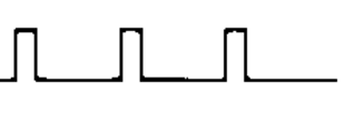
제 8 도는 종래장치의 개략적인 구성을 나타낸 단면도.
제 9 도는 종래장치에서의 신호파형도이다.
* 도면의 주요부분에 대한 부호의 설명
C0, C1, C2 : 기생용량 14 : 접촉구멍
21 : 실리콘 반도체기판 22 : 웰영역
23 : 필드산화막 24, 28 : 소오스영역
25, 29 : 드레인영역 26 : N챈널 MOS트랜지스터
27, 31 : 게이트전극 30 : P챈널 MOS트랜지스터
32 : 층간절연막 33, 37 : 소오스배선
34 : 드레인배선 35, 38 : 소오스인출전극
36 : 드레인인출전극
11, 12, 13, 15, 39, 41, 42, 44, 45, 46, 49, 50, 51, 81, 82 : 배선
47, 48, 52, 53 : 접속전극 10, 80 : 절연층
[산업상의 이용분야]
본 발명은 배선상호간의 신호간섭을 방지하도록 된 반도체접적회로에 관한 것이다.
[종래의 기술 및 그 문제점]
최근 반도체집적회로에 대해 고집적화가 강력하게 요구되고 있는 바, 소자의 미세화기술과 다층배선화기술등이 진보됨에 따라 그 집적도는 더욱 증가되고 있고, 또는 소자의 미세화기술에 따른 배선폭 및 배선상호간의 거리의 축소화에 따라 종래에는 거의 문제로 되지 않았던 배선간의 신호간섭에 의해 정확한 신호전달이 곤란하게 되었다.
제 8 도는 종래의 반도체집적회로의 개략적인 구성을 나타낸 단면도로서, 도면중 절연층(80)내에는 제 1 층째의 도전체층으로 구성된 배선(81)와 제 2 층째 의 도전체층으로 구성된 배선(82)이 배치되어 있고, 상기 양 배선(81, 82)의 상호간에는 기생적으로 용량(C0, C1, C2)이 발생되어 있다.
그중 상기 용량(C0)은 상기 양 배선(81, 82)을 연결하는 최단의 거리간에서 발생하고 있고, 상기 용량(C1, C2)은 각각 상기 양 배선(81, 82)간의 양측으로부터 타원형태로 발생되는데, 통상적으로 상기 용량값사이에는 C0〉C1, C2로 되는 관계가 성립한다.
여기서 상기 양 배선(81, 82)간에는 각각 다른 신호 또는 전압이 전달되는 바, 예컨대 상기 한쪽의 배선(81)에는 제 9 도에 나타낸 파형도(a)와 같은 아날로그신호가 전달되고, 다른 쪽의 배선(82)에는 제 9 도에 나타낸 파형도(b)와 같은 디지탈신호가 전달되는 경우, 상기 기생용량(C0, C1, C2)을 통해 신호간섭이 발생하게 됨으로써 아날로그신호는 디지탈신호의 영향을 받게 되어 제 9c 도에 나타낸 바와 같이 왜곡이 발생하게 된다.
이 결과 배선(81)에서는 정확한 아날로그신호를 전달할 수 없게 된다. 또 미세화 및 다층화된 배선구조를 갖춘 반도체집적회로에서는 주위 배선과의 신호간섭의 기회가 많아지게 되어 정확한 신호전달이 더욱 곤란하게 된다.
상기한 바와 같이 종래에는 소자의 미세화 및 다층배선화에 따라 배선상호간에서 신호간섭이 증대함으로써 정확한 신호전달이 곤란하게 되는 결점이 있었다.
[발명의 목적]
본 발명은 상기한 점을 감안해서 발명된 것으로, 소자의 미세화 및 다층배선화를 도모해도 배선상호간에서 신호간섭의 증대가 방지되어 정확하게 신호를 전달할 수 있도록 된 반도체집적회로를 제공하는데 그목적이 있다.
[발명의 구성]
상기 목적을 달성하기 위한 본발명은 반도체기판과, 이 기판상에 형성된 절연층, 이 절연층내에 형성되어 각각 서로다른 신호를 전달하는 배선으로 사용 되는 다층구조의 복수의 제 1 도전체층 및, 이 복수의 제 1 도전체중 인접하는 2개의 제 1 도전층의 상호간에 설치되며 일정전위로 고정된 신호간섭방지용의 제 2 도전체층을 구비하여 구성된 것을 특징으로 한다.
[작용]
상기와 같이 구성된 본 발명은, 서로다른 신호를 전달하는 배선으로 사용되는 복사의 제 1 도전체중 인접한 2개의 제 1 도전체층의 상호간에 발생되는 기생적인 용량의 값이 충분하게 작아지게 되어 양 배선간의 신호간섭이 감소하게 된다.
[실시예]
이하 예시도면에 의거해서 본 발명에 따른 각 실시예를 상세히 설명한다.
제 1 도는 본 발명에 따른 반도체집적회로의 개략적인 구성의 나타낸 단면도로서, 도면중 절연층(10)내에는 제 1 층째의 도전체층에 의해 배선(11)이 구성되고, 제 2 층째의 도전체층에 의해 배선(12)이 각각 구성되며, 상기 양 배선 (11, 12)상호간에는 제 1 층째의 도전체층에 의해 구성되는 (13)과 제 2 층째의 도전체층에 의해 구성되는 접촉구멍(14)을 매개해서 상기 배선(13)와 전기적으로 접속된 배선(15)이 배치되어 있다. 그리고 상기 양 배선(13, 15)은 일정전위, 예컨대, 접지전위와 더불어 전원전위로 고정되어 있다.
이와 같이 각각 서로다른 신호가 전달되는 배선(11)와 배선(12)간에 일정전위로 고정된 배선을 배치시킴으로써 상기 제 8 도중의 기생용량(C0)에 대등한 용량은 발생하지 않고, 용량(C1, C2)만이 기생용량으로서 발생하게 된다.
그러나 상기 한 바와 같이 통상 C0〉C1, C2라는 관계가 성립해서 용량(C1, C2)이 충분하게 작은 값으로 되기 때문에 용량(C1, C2)만을 개재시키는 것에 의해 배선(11, 12)간에 발생하는 신호간섭도 충분하게 작게 할 수 있게 된다.
다음에 본 발명의 여러 종류의 실시예의 이용해서 설명한다.
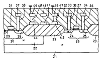
제 2 도는 본 발명의 1층배선구조의 CMOS형 반도체집적회로에다 실시한 경우의 일부분의 소자구조를 나타낸 단면도로서, 도면중 참조부호 21은 P형실리콘반도체기판, 22는 상기 기판(21)내에 형성된 N형웰 영역, 23은 소자분리용의 필드산화막, 24 및 25는 상기 기판(21)의 표면영역에 형성된 N형 확산영역으로 이루어진 N챈널 MOS트랜지스터(30)의 소오스와 드레인영역, 역, 31은 예컨대 다결정실리콘으로 구성된 P챈널 MOS트랜지스터(30)의 게이트전극, 32은 기판표면상에 설치된 BPSG(보론, 인, 실리콘유리)막 또는 PSG(인, 실리콘유리)막등으로 이루어진 층간절영막, 33은 예컨대 알루미늄 등의 금속을 이용해서 상기 층간절연막(32)내에 형성시킨 N챈널 MOS트랜지스터(26)의 소오스배선, 34는 마찬가지로 예컨대 알루미늄등의 금속을 이용해서 상기 층간절연막(32)내에 형성시킨 상기 N챈널 MOS트랜지스터(26)의 드레인 배선, 35는 상기 소오스배선(33)와 동일한 도전체재료인 알루미늄 등의 금속을 이용해서 구성되어 상기 소오스배선(33)와 소오스영역(24)을 접속시키는 소오스인출전극, 36은 상기 드레인배선(34)과 동일한 도전체재료인 알루미늄 등의 금속의 이용해서 구성되어 상기 드레인배선(34)와 드레인영역(25)을 접속시키는 드레인인출전극, 37은 예컨대 알루미늄 등의 금속을 이용해서 상기 층간절연막(32)내에 형성시킨 P챈널 MOS트랜지스터(30)의 소오스배선, 38은 상기 소오스배선(37)와 동일한 도전체재료인 알루미늄 등의 금속을 이용해서 구성되어 상기 P챈널 MOS트랜지스터(30)측의 소오스배선(37)와 소오스영역 (28)을 접속시키는 소오스인출전극이다.
그리고 상기 층간절연막(32)내의 상기 양 배선(33, 37)상호간에는 예컨대 알루미늄같은 금속으로 구성되어 일정전위, 예컨대 접지전위로 고정된 배선(38)이 형성되어 있다.
한편 상기 제 2 도에서는 P챈널 MOS트랜지스터(30)측의 드레인배선과 드레인인출전극의 도시를 생략하였다.
본 실시예에 따른 집적회로에서 상기 제 1 도중의 배선(11)에 대응하는 배선은 예컨대 N챈널 MOS트랜지스터(26)측의 소오스배선(33)이고, 상기 제 1 도중의 배선(12)에 대응하는 배선은 예컨대 P챈널 MOS트린지스터(30)측의 소오스배선(37)이며, 또 상기 제 1 도중의 배선(13)또는 배선(15)에 대응하는 배선은 양 소오스배선(33, 37)상호간에 배치된 배선(39)이다.
상기와 같은 구성에 있어서, 양 소오스배선(33, 37)상호간에 배치된 배선 (39)이 접지전위로 고정되어 있기 때문에 상기 양 소오스배선(33, 37)에 각각 다른 신호가 전달되어도 배선(39)이 존재함으로써 양 배선(33, 37)간에 발생하는 기생용략의 값이 작아지게 된다. 이 결과 배선의 미세화에 따라 각 배선상호간의 거리가 축소되어도 양 소오스배선(33, 37)상호간에서 신호간섭의 발생을 충분하게 작게 할 수 있으므로 정확하게 신호를 전달할 수 있게 된다.
제 3 도는 본 발명을 2층배선구조의 CMOS형 반도체집적회로에다 실시한 경우의 일부분의 소자구조를 나타낸 단면도로서, 제 2 도와 대응하는 장소에는 동일한 참조부호를 붙이고 그에 대한 상세한 설명은 생략한다.
본 실시예에 따른 집적회로에서는 상기 필드산화막(23)에 예컨대 알루미늄 등의 금속으로 구성된 배선(41)이 추가되어 있고, 또 층간절연막(32)내에 상기 배선(41)의 상부에 대응하는 위치에 예컨대 알루미늄 등의 금속을 이용해서 구성된 배선(42)이 추가 되어 있는데, 상기 양 배선(41, 42)은 각각 도시되지 않는 다른 회로끼리를 접속시키기 위한 배선으로서 사용되고 있다. 그리고 상기 배선(41)과 상기 N챈널 MOS트랜지스터(26)측의 소오스인출전극 (35)간의 필드산화막(23)상에는 상기 배선(41)와 동일한 도전체재료인 알루미늄 등의 금속으로 구성된 배선(43)이 추가 되어 있고 상지 배선(41)와 상기 P챈널 MOS트랜지스터(30)측의 소오스인출전극(28)간의 필드산화막(23) 상에도 상기 배선(41)와 동일한 도전체재료인 알루미늄 등의 금속으로 구성된 배선(44)이 추가 되어 있다. 또는 층간절연막(32)내에는 상기 배선(42)과 상기 N챈널 MOS트랜지스터(26)측의 소오스배선(33)간에 상기 배선(42)와 동일한 층이면서 동일한 도전체재료인 알루미늄 등의 금속으로 구성된 배선(45) 이 추가 되어 있고, 상기 배선(42)와 상기 P챈널 MOS트랜지스터(30)측의 소오스배선(37)간에도 알루미늄 등의 금속으로 구성된 배선(46)이 추가되어 있다. 그리고 상기 각 배선(43, 44, 45, 46)은 각각 독립적으로 도시되지 않는 장소에 일정전위, 예컨대 접지전위로 고정되어 있다.
상기 실시예에 따른 집적회로에서는 배선(42)과 소오스배선(33)상호간에 접지전위로 고정된 배선(45)이 배치되어 있고, 배선(42)와 소오스배선(37) 상호 간에 접지전위로 고정된 배선(46)이 각각 배치되어 있기 때문에 양 소오스배선(33, 37)와 배선(42)에 따른 신호가 전달되어도 신호의 상호간섭의 발생을 충분히 작게 할 수 있으므로 정확하게 신호를 전달할 수 있게 된다.
또 상기 실시예에서는 배선(41)와 소오스인출전극(35)상호간에도 접지전위로 고정된배선(43)이 배치되어 있고, 배선(41)와 소오스인출전극(38) 상호간에도 접지전위로 고정된 배선(44)이 각각 배치되어 있기 때문에 배선(41)와 소오스인출전극(35)간의 신호간섭 및, 배선(41)와 소오스 인출전극(38)간의 신호간섭도 각각 충분히 작게할 수 있게 된다.
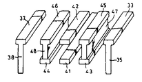
제 4 도는 본 발명의 상기 제 3 도의 경우와 동일한 2층배선구조의 CMOS형 반도체집적회로에다 실시한 경우의 일부분의 소자구조를 나타낸 단면도로서, 제 3 도와 대응하는 장소에는 동일한 참조부호를 붙이고 그에 대한 상세한 설명은 생략한다.
본 실시예에 따른 집적회로에서는 상기 제 3 도중 필드산화막(23)상에 형성된 상기 배선(43)과 층간절연막(32)내에 형성된 배선(45)이 층간절연막(32)에 형성된 관통구멍을 메우도록 설치되는데, 예컨대, 배선(45)과 동일한 도전체재료인 알루미늄 등의 금속으로 구성된 접속전극(47)을 이용해서 전기적으로 접속시킨다. 또 상기 필드산화막(23)상에 형성된 상기 배선(44)과 층간절연막(32)내에 형성된 상기 배선(46)이 층간절연막(32)에 형성된 관통구멍을 메우도록 설치되는데, 예컨대 배선(46)와 동일한 도전체재료인 알루미늄등의 금속으로 구성된 접속전극(48)을 이용해서 전기적으로 접속시키도록 구성된다.
제 5 도는 상기 제 4 도에 나타낸 실시예장치로부터 소오스배선(33, 37)과 소오스인출전극(35, 38), 배선(41, 42), 배선(43, 44) 및 접속전극(47, 48)을 골라서 나타낸 사시도로서, 도시한 바와 같이 접속전극(47, 48)을 이용해서 접속된 재선(43, 45) 및 배선(44, 46)은 평면적으로 그 양측에 배치된 소오스배선(33, 37)와 배선(41, 42)각각의 연장방향에 따라 벽상(壁狀)으로 형성 되어, 소오스배선전극(33, 37)과 배선(41, 42)을 각각 분리하고 있다.
상기한 바와 같이 배선이 다층화된 집적회로에서는 일정전위로 고정된 각각 다른 층의 배선을 접속전극을 이용해서 전기적으로 접속시키고, 이들의 배선을 벽상으로 구성시킴으로써 신호가 타원형태로 발생되는 것을 방지하는 효과가 향상되어 그양측에 배치된 배선상호간의 신호간섭의 발생을 역시 작게 할 수 있게 된다.
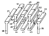
제 6 도는 본 발명을 3층배선구조의 CMOS형 반도체집적회로에다 실시한 경우의 일부분의 소자구조를 나타낸 단면도로서, 상기 제 4 도와 대응하는 장소에는 동일한 참조부호를 붙이고 그에 대한 상세한 설명은 생략한다.
본 실시예에 따른 집적회로에서는, 상지 배선(41, 43, 44)을 제 1 층째의 예컨대 알루미늄등으로 이루어진 금속을 이용해서 구성하고, 상기 배선(42, 45, 46 )을 제 2 층째의 예컨대 알루미늄등으로 이루어진 금속을 이용해서 구성되면서 층간절연막(32)내에 새로운 제3층째의 예컨대 알루미늄등으로 이루어진 금속을 이용해서 구성된 배선(49, 50, 51)을 설치하도록 한 것이다. 그리고 상기 배선(49, 50, 51)중 배선(49)은 상기 배선(41, 42)과 마찬가지로 도시되지 않는 다른 회로끼리 접속시키기 위한 배선으로 사용되고, 또는 배선(50, 51)은 신호간섭방지용의 배선으로서 사용된다. 상기 배선(50)와 상기 배선(45)은 예컨대 배선(50)와 동일한 도전체재료인 알루미늄 등의 금속으로 구성되고, 층간절연막(32)에 형선된 관통구멍의 메우도록 설치한 접속전극(52)을 이용해서 전기적으로 접속되어 있다. 마찬가지로 배선(51)과 상기 배선(46)은 예컨대 배선(51)와 동일한 도전체재료인 알루미늄 등의 금속으로 구성되고, 층간 절연막 (32)에 형선된 관통구멍을 메우도록 설치된 접속전극(52)을 이용해서 전기적으로 접속되어 있다.
제 7 도는 상기 제 6 도에 나타낸 실시예장치로부터 소오스배선(33, 37)과 소오스인출전극(35, 38), 배선(41, 42, 43, 44, 45, 46, 49, 50, 51) 및 접속전극(47, 48, 52, 53)을 골라서 나타낸 사시도로서, 동시한 바와 같이 접속전극(47, 52)과 접속전극(48, 53)을 이용해서 각각 접속된 3층의 배선(43, 45, 50) 및 배선(44, 46, 51)은 평면적으로 그양측에 배치된 소오스배선 (33, 37) 및 배선(41, 42, 49)각각의 연장방향에 따라 벽상으로 형성되고, 소오스배선(33, 37)와 배선(41, 42, 49)을 각각 분리하고 있다.
상기와 같은 3층배선구조의 집적회로에서는 소자의 미세화에 따라 배선 상호간의 거리가 축소되면 동일층의 배선상호간 뿐만 아니라 다른 층의 배선상호간의 신호간섭도 문제로 된다. 그러나 일정전위로 고정된 각각 다른 층의 배선 을 접속전극을 이용해서 접속시켜 벽상으로 구성시킴으로써 신호가 타원 형태로 발생되는 것을 방지하는 효과가 향상되어, 그 양측에 배치된 배선상호간의 신호간섭의 발생을 극도로 작게할 수 있게 됨에 따라 각 배선에 정확한 신호를 전달할 수 있게 된다.
또 본 발명은 상기 각 실시예에 한정되지 않고 여러 가지로 변형해서 실시할 수 있는 바, 예컨대 상기 각 실시예에서는 본발명을 CMOS형 반도체집적회로에다 실시하면서 소오스배선끼리 또는 소오스배선과 다른 배선간의 신호간섭방지를 도모한 경우에 대해서만 설명했지만, 이것은 신호간섭이 문제로 되는 반도체집적회로내의 모든 배선에 대해 실시할 수 있다. 또 신호간섭방지용의 배선은 접지전위로 고정하는 경우에 대해서만 설명했지만, 이것은 일정전위이면 어떠한 전위로 고정해도 되고, 또는 신호간섭방지용의 배선의 전위를 여러 가지 값으로 설정해도 된다.
[발명의 효과]
상기한 바와 같이 본 발명에 의하면, 소자의 미세화 및 다층배선화를 도모해도 배선상호간에서 신호간섭의 증대가 방지될 수 있어서 정확한 신호를 전달할 수 있는 반도체집적회로를 제공할 수 있게 된다.
Claims (3)
- 반도체기판(21)와, 이 기판(21)상에 형성된 절연층(32), 이 절연층(32)내에 형성되어 각각 서로다른 신호를 전달하는 배선으로 사용되는 다층구조의 복수의 제 1 도전체층(33, 37) 및, 이 복수의 제 1 도전체층중 인접하는 2개의 제 1 도전체층(33, 37)의 상호간에 설치되며 일정전위로 고정된 신호간섭방지용의 제 2 도전체층(39)을 구비해서 구성된 것을 특징으로 하는 반도체집적회로.
- 제 1 항에 있어서, 상지 제 2 도전체층(39)이 상기 절연층(32)내에 형성된 적어도 2층 이상의 도전체층(44, 46)으로 대체되어 구성된 것을 특징으로 하는 반도체집적회로.
- 제 2 항에 있어서, 상지 제 2 도전체층(39)에 대체되어 구성되는 적어도 2층이상의 도전체층(44, 46)이 상기 절연층(32)내에 형성된 제 3 도전체층(48)을 매개해서 전기적으로 접속되고, 상기 제 3 도전체층(48)이 상기 2개의 제 1 도전체층(33, 37)의 연장방향에 따라 상기 2개의 제 1 도전체층(33, 37)을 분리하도록 벽상으로 형성된 것을 특징으로 하는 반도체집적회로.
Applications Claiming Priority (3)
| Application Number | Priority Date | Filing Date | Title |
|---|---|---|---|
| JP63141769A JPH021928A (ja) | 1988-06-10 | 1988-06-10 | 半導体集積回路 |
| JP63-141769 | 1988-06-10 | ||
| JP88-141769 | 1988-06-10 |
Publications (2)
| Publication Number | Publication Date |
|---|---|
| KR900001002A KR900001002A (ko) | 1990-01-31 |
| KR920004179B1 true KR920004179B1 (ko) | 1992-05-30 |
Family
ID=15299748
Family Applications (1)
| Application Number | Title | Priority Date | Filing Date |
|---|---|---|---|
| KR1019890008007A KR920004179B1 (ko) | 1988-06-10 | 1989-06-10 | 반도체집적회로 |
Country Status (5)
| Country | Link |
|---|---|
| US (1) | US4958222A (ko) |
| EP (1) | EP0353426B1 (ko) |
| JP (1) | JPH021928A (ko) |
| KR (1) | KR920004179B1 (ko) |
| DE (1) | DE68929486T2 (ko) |
Families Citing this family (50)
| Publication number | Priority date | Publication date | Assignee | Title |
|---|---|---|---|---|
| JPH0828467B2 (ja) * | 1988-11-15 | 1996-03-21 | 株式会社東芝 | 半導体装置 |
| JP2580301B2 (ja) * | 1988-12-27 | 1997-02-12 | 株式会社日立製作所 | 半導体集積回路装置 |
| US5192716A (en) * | 1989-01-25 | 1993-03-09 | Polylithics, Inc. | Method of making a extended integration semiconductor structure |
| US5055907A (en) * | 1989-01-25 | 1991-10-08 | Mosaic, Inc. | Extended integration semiconductor structure with wiring layers |
| JP2507618B2 (ja) * | 1989-07-21 | 1996-06-12 | 株式会社東芝 | 半導体集積回路装置の製造方法 |
| JP2598328B2 (ja) * | 1989-10-17 | 1997-04-09 | 三菱電機株式会社 | 半導体装置およびその製造方法 |
| US5256590A (en) * | 1989-11-24 | 1993-10-26 | Mitsubishi Denki Kabushiki Kaisha | Method of making a shielded semiconductor device |
| JPH03165058A (ja) * | 1989-11-24 | 1991-07-17 | Mitsubishi Electric Corp | 半導体装置 |
| US5182625A (en) * | 1990-04-26 | 1993-01-26 | Fuji Xerox Co., Ltd. | Image sensor and method of manufacturing the same |
| JPH0410624A (ja) * | 1990-04-27 | 1992-01-14 | Hitachi Ltd | 半導体集積回路 |
| JP2746730B2 (ja) * | 1990-05-17 | 1998-05-06 | 富士通株式会社 | 半導体記憶装置 |
| EP0460857B1 (en) * | 1990-05-31 | 1997-03-19 | Canon Kabushiki Kaisha | Method for producing a semiconductor device with a high density wiring structure |
| JPH0750710B2 (ja) * | 1990-06-06 | 1995-05-31 | 富士ゼロックス株式会社 | 多層配線構造 |
| US5122859A (en) * | 1990-06-29 | 1992-06-16 | Texas Instruments Incorporated | Iterative self-aligned contact metallization process |
| EP0480580A3 (en) * | 1990-09-10 | 1992-09-02 | Canon Kabushiki Kaisha | Electrode structure of semiconductor device and method for manufacturing the same |
| JPH04267586A (ja) * | 1991-02-22 | 1992-09-24 | Nec Corp | 同軸配線パターンおよびその形成方法 |
| US5151769A (en) * | 1991-04-04 | 1992-09-29 | General Electric Company | Optically patterned RF shield for an integrated circuit chip for analog and/or digital operation at microwave frequencies |
| JPH05136125A (ja) * | 1991-11-14 | 1993-06-01 | Hitachi Ltd | クロツク配線及びクロツク配線を有する半導体集積回路装置 |
| KR940008132B1 (ko) * | 1991-11-28 | 1994-09-03 | 삼성전자 주식회사 | 신호선간의 잡음을 억제하는 메모리 소자 |
| US5196920A (en) * | 1992-04-21 | 1993-03-23 | Mitsubishi Denki Kabushiki Kaisha | Semiconductor integrated circuit device for limiting capacitive coupling between adjacent circuit blocks |
| JP2876963B2 (ja) * | 1993-12-15 | 1999-03-31 | 日本電気株式会社 | 半導体装置 |
| JP3283984B2 (ja) * | 1993-12-28 | 2002-05-20 | 株式会社東芝 | 半導体集積回路装置 |
| US5689134A (en) * | 1995-01-09 | 1997-11-18 | Lsi Logic Corporation | Integrated circuit structure having reduced cross-talk and method of making same |
| AU2187397A (en) * | 1996-03-22 | 1997-10-10 | Telefonaktiebolaget Lm Ericsson (Publ) | Semiconductor device shielded by an array of electrically conducting pins and a method to manufacture such a device |
| KR100243265B1 (ko) * | 1996-10-16 | 2000-03-02 | 윤종용 | 클럭 라인을 구비하는 반도체 칩 |
| JP3681865B2 (ja) | 1997-03-31 | 2005-08-10 | 三菱電機株式会社 | 光パルス位置検出回路及び光パルス位置検出方法 |
| KR19980084130A (ko) * | 1997-05-21 | 1998-12-05 | 윤종용 | 전자파 차폐증을 가진 반도체장치 및 그 제조방법 |
| JP3501620B2 (ja) * | 1997-05-26 | 2004-03-02 | 株式会社 沖マイクロデザイン | 半導体集積回路 |
| US6828230B2 (en) | 1997-09-12 | 2004-12-07 | Micron Technology, Inc. | Integrated circuit having conductive paths of different heights formed from the same layer structure and method for forming the same |
| KR100308871B1 (ko) * | 1998-12-28 | 2001-11-03 | 윤덕용 | 동축 구조의 신호선 및 그의 제조 방법 |
| JP3219067B2 (ja) * | 1999-01-08 | 2001-10-15 | 日本電気株式会社 | 集積回路 |
| US6307252B1 (en) * | 1999-03-05 | 2001-10-23 | Agere Systems Guardian Corp. | On-chip shielding of signals |
| KR20010009697A (ko) | 1999-07-13 | 2001-02-05 | 윤종용 | 차폐선을 구비한 반도체 집적회로 |
| US7294935B2 (en) * | 2001-01-24 | 2007-11-13 | Hrl Laboratories, Llc | Integrated circuits protected against reverse engineering and method for fabricating the same using an apparent metal contact line terminating on field oxide |
| US7259640B2 (en) | 2001-12-03 | 2007-08-21 | Microfabrica | Miniature RF and microwave components and methods for fabricating such components |
| US9614266B2 (en) | 2001-12-03 | 2017-04-04 | Microfabrica Inc. | Miniature RF and microwave components and methods for fabricating such components |
| US7239219B2 (en) * | 2001-12-03 | 2007-07-03 | Microfabrica Inc. | Miniature RF and microwave components and methods for fabricating such components |
| FR2839581B1 (fr) * | 2002-05-07 | 2005-07-01 | St Microelectronics Sa | Circuit electronique comprenant un condensateur et au moins un composant semiconducteur, et procede de conception d'un tel circuit |
| JP2004040042A (ja) * | 2002-07-08 | 2004-02-05 | Fujitsu Ltd | 半導体記憶装置 |
| US6657285B1 (en) * | 2002-07-08 | 2003-12-02 | Alcor Micro, Corp. | Semiconductor anti-interference band for integrated circuit |
| US10297421B1 (en) | 2003-05-07 | 2019-05-21 | Microfabrica Inc. | Plasma etching of dielectric sacrificial material from reentrant multi-layer metal structures |
| KR100469892B1 (ko) * | 2003-07-14 | 2005-02-02 | (주) 팜텍21 | 농작물의 보존성 향상을 위한 육계나무 수피 추출물 |
| JP4867157B2 (ja) * | 2004-11-18 | 2012-02-01 | ソニー株式会社 | 高周波トランジスタの設計方法、および、マルチフィンガーゲートを有する高周波トランジスタ |
| US7576382B2 (en) | 2005-02-02 | 2009-08-18 | Ricoh Company, Ltd. | Semiconductor integrated device and method of providing shield interconnection therein |
| US8853832B2 (en) * | 2009-01-22 | 2014-10-07 | Stmicroelectronics Inc. | Methods and apparatus for reducing coupling in a MOS device |
| JP2012164882A (ja) * | 2011-02-08 | 2012-08-30 | Toshiba Corp | 半導体装置 |
| JP5364743B2 (ja) * | 2011-03-01 | 2013-12-11 | 株式会社東芝 | 半導体装置 |
| CN102903698B (zh) * | 2012-10-25 | 2017-02-08 | 上海华虹宏力半导体制造有限公司 | 半导体器件及集成电路 |
| KR102322765B1 (ko) * | 2015-06-22 | 2021-11-08 | 삼성디스플레이 주식회사 | 표시 장치 |
| LV15796A (lv) | 2022-06-16 | 2023-12-20 | Jifteco, Sia | Dzīvnieku repelents |
Family Cites Families (20)
| Publication number | Priority date | Publication date | Assignee | Title |
|---|---|---|---|---|
| US3533023A (en) * | 1967-09-19 | 1970-10-06 | Motorola Inc | Multilayered circuitry interconnections with integral shields |
| US3573571A (en) * | 1967-10-13 | 1971-04-06 | Gen Electric | Surface-diffused transistor with isolated field plate |
| US3518506A (en) * | 1967-12-06 | 1970-06-30 | Ibm | Semiconductor device with contact metallurgy thereon,and method for making same |
| JPS4940889A (ko) * | 1972-08-25 | 1974-04-17 | ||
| NL7302767A (ko) * | 1973-02-28 | 1974-08-30 | ||
| JPS5255881A (en) * | 1975-11-04 | 1977-05-07 | Matsushita Electronics Corp | Semiconductor integrated circuit |
| JPS54157092A (en) * | 1978-05-31 | 1979-12-11 | Nec Corp | Semiconductor integrated circuit device |
| JPS5811750B2 (ja) * | 1979-06-04 | 1983-03-04 | 株式会社日立製作所 | 高耐圧抵抗素子 |
| JPS56126956A (en) * | 1980-03-11 | 1981-10-05 | Fujitsu Ltd | Semiconductor device |
| JPS5727962A (en) * | 1980-07-19 | 1982-02-15 | Tatsurou Okamura | Construction material |
| JPS57104243A (en) * | 1980-12-20 | 1982-06-29 | Toshiba Corp | Semiconductor device |
| JPS5853845A (ja) * | 1981-09-26 | 1983-03-30 | Fujitsu Ltd | 半導体集積回路装置 |
| JPS58190045A (ja) * | 1982-04-30 | 1983-11-05 | Fujitsu Ltd | 半導体装置用パツケ−ジ |
| JPS5994849A (ja) * | 1982-11-24 | 1984-05-31 | Nec Corp | 半導体集積回路装置 |
| US4514749A (en) * | 1983-01-18 | 1985-04-30 | At&T Bell Laboratories | VLSI Chip with ground shielding |
| US4580156A (en) * | 1983-12-30 | 1986-04-01 | At&T Bell Laboratories | Structured resistive field shields for low-leakage high voltage devices |
| JPS6198477A (ja) * | 1984-10-19 | 1986-05-16 | Nec Corp | Cadによる配線設計システム |
| JPS61230340A (ja) * | 1985-04-05 | 1986-10-14 | Nec Ic Microcomput Syst Ltd | 半導体集積回路装置 |
| JPH0669040B2 (ja) * | 1985-05-13 | 1994-08-31 | 株式会社東芝 | 光半導体装置 |
| DE3641299A1 (de) * | 1986-12-03 | 1988-06-16 | Philips Patentverwaltung | Integrierte halbleiter-schaltung mit mehrlagenverdrahtung |
-
1988
- 1988-06-10 JP JP63141769A patent/JPH021928A/ja active Granted
-
1989
- 1989-06-09 US US07/363,759 patent/US4958222A/en not_active Expired - Lifetime
- 1989-06-09 EP EP89110480A patent/EP0353426B1/en not_active Expired - Lifetime
- 1989-06-09 DE DE68929486T patent/DE68929486T2/de not_active Expired - Fee Related
- 1989-06-10 KR KR1019890008007A patent/KR920004179B1/ko not_active IP Right Cessation
Also Published As
| Publication number | Publication date |
|---|---|
| EP0353426A2 (en) | 1990-02-07 |
| JPH021928A (ja) | 1990-01-08 |
| DE68929486T2 (de) | 2004-07-22 |
| DE68929486D1 (de) | 2003-11-13 |
| US4958222A (en) | 1990-09-18 |
| EP0353426B1 (en) | 2003-10-08 |
| JPH0570302B2 (ko) | 1993-10-04 |
| KR900001002A (ko) | 1990-01-31 |
| EP0353426A3 (en) | 1991-07-31 |
Similar Documents
| Publication | Publication Date | Title |
|---|---|---|
| KR920004179B1 (ko) | 반도체집적회로 | |
| US6787873B2 (en) | Semiconductor device for providing a noise shield | |
| US5440163A (en) | CMOS ESD protection structure | |
| US5087955A (en) | Input-output circuit of reduced device area for semicustom semiconductor integrated circuit | |
| EP0080361A2 (en) | Complementary metal-oxide semiconductor integrated circuit device of master slice type | |
| US5111271A (en) | Semiconductor device using standard cell system | |
| US7595561B2 (en) | Semiconductor device including multiple rows of peripheral circuit units | |
| KR100197989B1 (ko) | 정전기 보호회로를 구비한 반도체장치 | |
| WO2020235082A1 (ja) | 半導体装置 | |
| US6856022B2 (en) | Semiconductor device | |
| US5691574A (en) | Semiconductor device capable of high speed operation and being integrated with high density | |
| US7239005B2 (en) | Semiconductor device with bypass capacitor | |
| US7190025B2 (en) | Array of pull-up transistors for high voltage output circuit | |
| WO2000067324A1 (fr) | Circuit integre, son procede de fabrication, et procede de production d'un dessin de masque | |
| US4974049A (en) | Semiconductor integrated circuit configured by using polycell technique | |
| US4523216A (en) | CMOS device with high density wiring layout | |
| US6441448B1 (en) | Semiconductor storage device | |
| US5796148A (en) | Integrated circuits | |
| JPH05275613A (ja) | 積層型半導体装置 | |
| JPH04360570A (ja) | 積層型半導体装置 | |
| JPH0666412B2 (ja) | 積層型半導体集積回路 | |
| JP3680488B2 (ja) | 半導体装置 | |
| JPH10294383A (ja) | 入力保護ダイオード | |
| JPS62249467A (ja) | 半導体集積回路装置 | |
| JPS62211945A (ja) | 半導体装置 |
Legal Events
| Date | Code | Title | Description |
|---|---|---|---|
| A201 | Request for examination | ||
| G160 | Decision to publish patent application | ||
| E701 | Decision to grant or registration of patent right | ||
| GRNT | Written decision to grant | ||
| FPAY | Annual fee payment |
Payment date: 20030430 Year of fee payment: 12 |
|
| LAPS | Lapse due to unpaid annual fee |