JP7143461B2 - semiconductor equipment - Google Patents
semiconductor equipment Download PDFInfo
- Publication number
- JP7143461B2 JP7143461B2 JP2021023311A JP2021023311A JP7143461B2 JP 7143461 B2 JP7143461 B2 JP 7143461B2 JP 2021023311 A JP2021023311 A JP 2021023311A JP 2021023311 A JP2021023311 A JP 2021023311A JP 7143461 B2 JP7143461 B2 JP 7143461B2
- Authority
- JP
- Japan
- Prior art keywords
- oxide semiconductor
- layer
- semiconductor layer
- content
- crystal
- Prior art date
- Legal status (The legal status is an assumption and is not a legal conclusion. Google has not performed a legal analysis and makes no representation as to the accuracy of the status listed.)
- Active
Links
- 239000004065 semiconductor Substances 0.000 title claims description 200
- 239000013078 crystal Substances 0.000 claims description 70
- 229910052733 gallium Inorganic materials 0.000 claims description 27
- 229910052725 zinc Inorganic materials 0.000 claims description 21
- 239000000203 mixture Substances 0.000 claims description 14
- 229910052738 indium Inorganic materials 0.000 claims description 12
- 239000010410 layer Substances 0.000 description 198
- 239000011701 zinc Substances 0.000 description 45
- 239000000758 substrate Substances 0.000 description 29
- 239000010408 film Substances 0.000 description 27
- 229910052760 oxygen Inorganic materials 0.000 description 27
- 238000004544 sputter deposition Methods 0.000 description 25
- 239000001301 oxygen Substances 0.000 description 24
- QVGXLLKOCUKJST-UHFFFAOYSA-N atomic oxygen Chemical compound [O] QVGXLLKOCUKJST-UHFFFAOYSA-N 0.000 description 22
- XKRFYHLGVUSROY-UHFFFAOYSA-N Argon Chemical compound [Ar] XKRFYHLGVUSROY-UHFFFAOYSA-N 0.000 description 20
- 238000010438 heat treatment Methods 0.000 description 20
- 239000007789 gas Substances 0.000 description 17
- 125000004429 atom Chemical group 0.000 description 15
- 238000004364 calculation method Methods 0.000 description 15
- 238000000034 method Methods 0.000 description 15
- 238000005530 etching Methods 0.000 description 14
- 239000000463 material Substances 0.000 description 13
- 230000015572 biosynthetic process Effects 0.000 description 12
- 238000004458 analytical method Methods 0.000 description 11
- 239000012298 atmosphere Substances 0.000 description 11
- 229910052782 aluminium Inorganic materials 0.000 description 10
- XAGFODPZIPBFFR-UHFFFAOYSA-N aluminium Chemical compound [Al] XAGFODPZIPBFFR-UHFFFAOYSA-N 0.000 description 10
- 229910052786 argon Inorganic materials 0.000 description 10
- 238000010586 diagram Methods 0.000 description 10
- 238000000851 scanning transmission electron micrograph Methods 0.000 description 9
- 229910005191 Ga 2 O 3 Inorganic materials 0.000 description 8
- 239000011521 glass Substances 0.000 description 8
- 239000010936 titanium Substances 0.000 description 8
- MYMOFIZGZYHOMD-UHFFFAOYSA-N Dioxygen Chemical compound O=O MYMOFIZGZYHOMD-UHFFFAOYSA-N 0.000 description 7
- XUIMIQQOPSSXEZ-UHFFFAOYSA-N Silicon Chemical compound [Si] XUIMIQQOPSSXEZ-UHFFFAOYSA-N 0.000 description 7
- 230000005669 field effect Effects 0.000 description 7
- 238000004519 manufacturing process Methods 0.000 description 7
- 229910052710 silicon Inorganic materials 0.000 description 7
- 239000010703 silicon Substances 0.000 description 7
- 229910007541 Zn O Inorganic materials 0.000 description 6
- 239000000460 chlorine Substances 0.000 description 6
- 229910001882 dioxygen Inorganic materials 0.000 description 6
- 229910052719 titanium Inorganic materials 0.000 description 6
- 239000004020 conductor Substances 0.000 description 5
- 239000010949 copper Substances 0.000 description 5
- 238000001312 dry etching Methods 0.000 description 5
- 238000011282 treatment Methods 0.000 description 5
- 238000001039 wet etching Methods 0.000 description 5
- 238000003775 Density Functional Theory Methods 0.000 description 4
- 229910052581 Si3N4 Inorganic materials 0.000 description 4
- RTAQQCXQSZGOHL-UHFFFAOYSA-N Titanium Chemical compound [Ti] RTAQQCXQSZGOHL-UHFFFAOYSA-N 0.000 description 4
- 229910045601 alloy Inorganic materials 0.000 description 4
- 239000000956 alloy Substances 0.000 description 4
- 239000011651 chromium Substances 0.000 description 4
- 230000007423 decrease Effects 0.000 description 4
- 229910052734 helium Inorganic materials 0.000 description 4
- 238000000731 high angular annular dark-field scanning transmission electron microscopy Methods 0.000 description 4
- VYPSYNLAJGMNEJ-UHFFFAOYSA-N silicon dioxide Inorganic materials O=[Si]=O VYPSYNLAJGMNEJ-UHFFFAOYSA-N 0.000 description 4
- HQVNEWCFYHHQES-UHFFFAOYSA-N silicon nitride Chemical compound N12[Si]34N5[Si]62N3[Si]51N64 HQVNEWCFYHHQES-UHFFFAOYSA-N 0.000 description 4
- 239000010409 thin film Substances 0.000 description 4
- QTBSBXVTEAMEQO-UHFFFAOYSA-N Acetic acid Chemical compound CC(O)=O QTBSBXVTEAMEQO-UHFFFAOYSA-N 0.000 description 3
- ZAMOUSCENKQFHK-UHFFFAOYSA-N Chlorine atom Chemical compound [Cl] ZAMOUSCENKQFHK-UHFFFAOYSA-N 0.000 description 3
- RYGMFSIKBFXOCR-UHFFFAOYSA-N Copper Chemical compound [Cu] RYGMFSIKBFXOCR-UHFFFAOYSA-N 0.000 description 3
- 229910052779 Neodymium Inorganic materials 0.000 description 3
- 239000012300 argon atmosphere Substances 0.000 description 3
- 229910052801 chlorine Inorganic materials 0.000 description 3
- 229910052802 copper Inorganic materials 0.000 description 3
- 238000000151 deposition Methods 0.000 description 3
- 230000008021 deposition Effects 0.000 description 3
- 238000009826 distribution Methods 0.000 description 3
- 239000000428 dust Substances 0.000 description 3
- 230000002349 favourable effect Effects 0.000 description 3
- 239000001307 helium Substances 0.000 description 3
- SWQJXJOGLNCZEY-UHFFFAOYSA-N helium atom Chemical compound [He] SWQJXJOGLNCZEY-UHFFFAOYSA-N 0.000 description 3
- APFVFJFRJDLVQX-UHFFFAOYSA-N indium atom Chemical compound [In] APFVFJFRJDLVQX-UHFFFAOYSA-N 0.000 description 3
- QEFYFXOXNSNQGX-UHFFFAOYSA-N neodymium atom Chemical compound [Nd] QEFYFXOXNSNQGX-UHFFFAOYSA-N 0.000 description 3
- 230000001681 protective effect Effects 0.000 description 3
- 229910052814 silicon oxide Inorganic materials 0.000 description 3
- IJGRMHOSHXDMSA-UHFFFAOYSA-N Atomic nitrogen Chemical compound N#N IJGRMHOSHXDMSA-UHFFFAOYSA-N 0.000 description 2
- VYZAMTAEIAYCRO-UHFFFAOYSA-N Chromium Chemical compound [Cr] VYZAMTAEIAYCRO-UHFFFAOYSA-N 0.000 description 2
- GYHNNYVSQQEPJS-UHFFFAOYSA-N Gallium Chemical compound [Ga] GYHNNYVSQQEPJS-UHFFFAOYSA-N 0.000 description 2
- 240000002329 Inga feuillei Species 0.000 description 2
- ZOKXTWBITQBERF-UHFFFAOYSA-N Molybdenum Chemical compound [Mo] ZOKXTWBITQBERF-UHFFFAOYSA-N 0.000 description 2
- NBIIXXVUZAFLBC-UHFFFAOYSA-N Phosphoric acid Chemical compound OP(O)(O)=O NBIIXXVUZAFLBC-UHFFFAOYSA-N 0.000 description 2
- 229910021417 amorphous silicon Inorganic materials 0.000 description 2
- 229910052804 chromium Inorganic materials 0.000 description 2
- 150000001875 compounds Chemical class 0.000 description 2
- 230000007547 defect Effects 0.000 description 2
- 238000001095 inductively coupled plasma mass spectrometry Methods 0.000 description 2
- 239000011810 insulating material Substances 0.000 description 2
- 150000002500 ions Chemical class 0.000 description 2
- 238000004599 local-density approximation Methods 0.000 description 2
- 238000001755 magnetron sputter deposition Methods 0.000 description 2
- 230000007246 mechanism Effects 0.000 description 2
- 229910052751 metal Inorganic materials 0.000 description 2
- 239000002184 metal Substances 0.000 description 2
- 229910052750 molybdenum Inorganic materials 0.000 description 2
- 239000011733 molybdenum Substances 0.000 description 2
- 150000004767 nitrides Chemical class 0.000 description 2
- 229910052757 nitrogen Inorganic materials 0.000 description 2
- TWNQGVIAIRXVLR-UHFFFAOYSA-N oxo(oxoalumanyloxy)alumane Chemical compound O=[Al]O[Al]=O TWNQGVIAIRXVLR-UHFFFAOYSA-N 0.000 description 2
- BPUBBGLMJRNUCC-UHFFFAOYSA-N oxygen(2-);tantalum(5+) Chemical compound [O-2].[O-2].[O-2].[O-2].[O-2].[Ta+5].[Ta+5] BPUBBGLMJRNUCC-UHFFFAOYSA-N 0.000 description 2
- 238000009832 plasma treatment Methods 0.000 description 2
- 230000008569 process Effects 0.000 description 2
- 229910052706 scandium Inorganic materials 0.000 description 2
- SIXSYDAISGFNSX-UHFFFAOYSA-N scandium atom Chemical compound [Sc] SIXSYDAISGFNSX-UHFFFAOYSA-N 0.000 description 2
- 239000002356 single layer Substances 0.000 description 2
- 229910052715 tantalum Inorganic materials 0.000 description 2
- GUVRBAGPIYLISA-UHFFFAOYSA-N tantalum atom Chemical compound [Ta] GUVRBAGPIYLISA-UHFFFAOYSA-N 0.000 description 2
- 229910001936 tantalum oxide Inorganic materials 0.000 description 2
- JBQYATWDVHIOAR-UHFFFAOYSA-N tellanylidenegermanium Chemical compound [Te]=[Ge] JBQYATWDVHIOAR-UHFFFAOYSA-N 0.000 description 2
- VZGDMQKNWNREIO-UHFFFAOYSA-N tetrachloromethane Chemical compound ClC(Cl)(Cl)Cl VZGDMQKNWNREIO-UHFFFAOYSA-N 0.000 description 2
- TXEYQDLBPFQVAA-UHFFFAOYSA-N tetrafluoromethane Chemical compound FC(F)(F)F TXEYQDLBPFQVAA-UHFFFAOYSA-N 0.000 description 2
- 150000003608 titanium Chemical class 0.000 description 2
- FAQYAMRNWDIXMY-UHFFFAOYSA-N trichloroborane Chemical compound ClB(Cl)Cl FAQYAMRNWDIXMY-UHFFFAOYSA-N 0.000 description 2
- WFKWXMTUELFFGS-UHFFFAOYSA-N tungsten Chemical compound [W] WFKWXMTUELFFGS-UHFFFAOYSA-N 0.000 description 2
- 229910052721 tungsten Inorganic materials 0.000 description 2
- 239000010937 tungsten Substances 0.000 description 2
- ZQXCQTAELHSNAT-UHFFFAOYSA-N 1-chloro-3-nitro-5-(trifluoromethyl)benzene Chemical compound [O-][N+](=O)C1=CC(Cl)=CC(C(F)(F)F)=C1 ZQXCQTAELHSNAT-UHFFFAOYSA-N 0.000 description 1
- 108091006149 Electron carriers Proteins 0.000 description 1
- 229910005555 GaZnO Inorganic materials 0.000 description 1
- CPELXLSAUQHCOX-UHFFFAOYSA-N Hydrogen bromide Chemical compound Br CPELXLSAUQHCOX-UHFFFAOYSA-N 0.000 description 1
- GRYLNZFGIOXLOG-UHFFFAOYSA-N Nitric acid Chemical compound O[N+]([O-])=O GRYLNZFGIOXLOG-UHFFFAOYSA-N 0.000 description 1
- HCHKCACWOHOZIP-UHFFFAOYSA-N Zinc Chemical compound [Zn] HCHKCACWOHOZIP-UHFFFAOYSA-N 0.000 description 1
- 238000005054 agglomeration Methods 0.000 description 1
- 230000002776 aggregation Effects 0.000 description 1
- 239000003513 alkali Substances 0.000 description 1
- 229910000147 aluminium phosphate Inorganic materials 0.000 description 1
- 239000005407 aluminoborosilicate glass Substances 0.000 description 1
- 239000005354 aluminosilicate glass Substances 0.000 description 1
- 229910052788 barium Inorganic materials 0.000 description 1
- DSAJWYNOEDNPEQ-UHFFFAOYSA-N barium atom Chemical compound [Ba] DSAJWYNOEDNPEQ-UHFFFAOYSA-N 0.000 description 1
- 230000005540 biological transmission Effects 0.000 description 1
- 239000005388 borosilicate glass Substances 0.000 description 1
- 150000001768 cations Chemical class 0.000 description 1
- 239000000919 ceramic Substances 0.000 description 1
- 230000007797 corrosion Effects 0.000 description 1
- 238000005260 corrosion Methods 0.000 description 1
- 238000009792 diffusion process Methods 0.000 description 1
- 239000001257 hydrogen Substances 0.000 description 1
- 229910052739 hydrogen Inorganic materials 0.000 description 1
- 125000004435 hydrogen atom Chemical class [H]* 0.000 description 1
- PJXISJQVUVHSOJ-UHFFFAOYSA-N indium(III) oxide Inorganic materials [O-2].[O-2].[O-2].[In+3].[In+3] PJXISJQVUVHSOJ-UHFFFAOYSA-N 0.000 description 1
- 239000011261 inert gas Substances 0.000 description 1
- 239000012212 insulator Substances 0.000 description 1
- 229910052742 iron Inorganic materials 0.000 description 1
- 238000010030 laminating Methods 0.000 description 1
- 239000004973 liquid crystal related substance Substances 0.000 description 1
- 239000013081 microcrystal Substances 0.000 description 1
- 229910021421 monocrystalline silicon Inorganic materials 0.000 description 1
- 229910017604 nitric acid Inorganic materials 0.000 description 1
- 239000012299 nitrogen atmosphere Substances 0.000 description 1
- GVGCUCJTUSOZKP-UHFFFAOYSA-N nitrogen trifluoride Chemical compound FN(F)F GVGCUCJTUSOZKP-UHFFFAOYSA-N 0.000 description 1
- 230000003647 oxidation Effects 0.000 description 1
- 238000007254 oxidation reaction Methods 0.000 description 1
- 238000000206 photolithography Methods 0.000 description 1
- 238000004698 pseudo-potential method Methods 0.000 description 1
- 239000010453 quartz Substances 0.000 description 1
- 238000001552 radio frequency sputter deposition Methods 0.000 description 1
- 238000005546 reactive sputtering Methods 0.000 description 1
- 239000011347 resin Substances 0.000 description 1
- 229920005989 resin Polymers 0.000 description 1
- 230000004044 response Effects 0.000 description 1
- 238000005001 rutherford backscattering spectroscopy Methods 0.000 description 1
- 229910052594 sapphire Inorganic materials 0.000 description 1
- 239000010980 sapphire Substances 0.000 description 1
- FDNAPBUWERUEDA-UHFFFAOYSA-N silicon tetrachloride Chemical compound Cl[Si](Cl)(Cl)Cl FDNAPBUWERUEDA-UHFFFAOYSA-N 0.000 description 1
- 238000004611 spectroscopical analysis Methods 0.000 description 1
- 239000010935 stainless steel Substances 0.000 description 1
- 229910001220 stainless steel Inorganic materials 0.000 description 1
- SFZCNBIFKDRMGX-UHFFFAOYSA-N sulfur hexafluoride Chemical compound FS(F)(F)(F)(F)F SFZCNBIFKDRMGX-UHFFFAOYSA-N 0.000 description 1
- 239000013077 target material Substances 0.000 description 1
- 238000002834 transmittance Methods 0.000 description 1
- 229910052984 zinc sulfide Inorganic materials 0.000 description 1
Images


Classifications
-
- H—ELECTRICITY
- H01—ELECTRIC ELEMENTS
- H01L—SEMICONDUCTOR DEVICES NOT COVERED BY CLASS H10
- H01L29/00—Semiconductor devices adapted for rectifying, amplifying, oscillating or switching, or capacitors or resistors with at least one potential-jump barrier or surface barrier, e.g. PN junction depletion layer or carrier concentration layer; Details of semiconductor bodies or of electrodes thereof ; Multistep manufacturing processes therefor
- H01L29/66—Types of semiconductor device ; Multistep manufacturing processes therefor
- H01L29/68—Types of semiconductor device ; Multistep manufacturing processes therefor controllable by only the electric current supplied, or only the electric potential applied, to an electrode which does not carry the current to be rectified, amplified or switched
- H01L29/76—Unipolar devices, e.g. field effect transistors
- H01L29/772—Field effect transistors
- H01L29/78—Field effect transistors with field effect produced by an insulated gate
- H01L29/786—Thin film transistors, i.e. transistors with a channel being at least partly a thin film
- H01L29/7869—Thin film transistors, i.e. transistors with a channel being at least partly a thin film having a semiconductor body comprising an oxide semiconductor material, e.g. zinc oxide, copper aluminium oxide, cadmium stannate
-
- H—ELECTRICITY
- H01—ELECTRIC ELEMENTS
- H01L—SEMICONDUCTOR DEVICES NOT COVERED BY CLASS H10
- H01L21/00—Processes or apparatus adapted for the manufacture or treatment of semiconductor or solid state devices or of parts thereof
- H01L21/02—Manufacture or treatment of semiconductor devices or of parts thereof
- H01L21/02104—Forming layers
- H01L21/02365—Forming inorganic semiconducting materials on a substrate
- H01L21/02518—Deposited layers
- H01L21/02521—Materials
- H01L21/02565—Oxide semiconducting materials not being Group 12/16 materials, e.g. ternary compounds
-
- H—ELECTRICITY
- H01—ELECTRIC ELEMENTS
- H01L—SEMICONDUCTOR DEVICES NOT COVERED BY CLASS H10
- H01L21/00—Processes or apparatus adapted for the manufacture or treatment of semiconductor or solid state devices or of parts thereof
- H01L21/02—Manufacture or treatment of semiconductor devices or of parts thereof
- H01L21/02104—Forming layers
- H01L21/02365—Forming inorganic semiconducting materials on a substrate
- H01L21/02612—Formation types
- H01L21/02617—Deposition types
- H01L21/02631—Physical deposition at reduced pressure, e.g. MBE, sputtering, evaporation
-
- H—ELECTRICITY
- H01—ELECTRIC ELEMENTS
- H01L—SEMICONDUCTOR DEVICES NOT COVERED BY CLASS H10
- H01L21/00—Processes or apparatus adapted for the manufacture or treatment of semiconductor or solid state devices or of parts thereof
- H01L21/02—Manufacture or treatment of semiconductor devices or of parts thereof
- H01L21/04—Manufacture or treatment of semiconductor devices or of parts thereof the devices having at least one potential-jump barrier or surface barrier, e.g. PN junction, depletion layer or carrier concentration layer
- H01L21/18—Manufacture or treatment of semiconductor devices or of parts thereof the devices having at least one potential-jump barrier or surface barrier, e.g. PN junction, depletion layer or carrier concentration layer the devices having semiconductor bodies comprising elements of Group IV of the Periodic System or AIIIBV compounds with or without impurities, e.g. doping materials
- H01L21/28—Manufacture of electrodes on semiconductor bodies using processes or apparatus not provided for in groups H01L21/20 - H01L21/268
- H01L21/28008—Making conductor-insulator-semiconductor electrodes
- H01L21/28017—Making conductor-insulator-semiconductor electrodes the insulator being formed after the semiconductor body, the semiconductor being silicon
- H01L21/28026—Making conductor-insulator-semiconductor electrodes the insulator being formed after the semiconductor body, the semiconductor being silicon characterised by the conductor
- H01L21/28079—Making conductor-insulator-semiconductor electrodes the insulator being formed after the semiconductor body, the semiconductor being silicon characterised by the conductor the final conductor layer next to the insulator being a single metal, e.g. Ta, W, Mo, Al
-
- H—ELECTRICITY
- H01—ELECTRIC ELEMENTS
- H01L—SEMICONDUCTOR DEVICES NOT COVERED BY CLASS H10
- H01L21/00—Processes or apparatus adapted for the manufacture or treatment of semiconductor or solid state devices or of parts thereof
- H01L21/02—Manufacture or treatment of semiconductor devices or of parts thereof
- H01L21/04—Manufacture or treatment of semiconductor devices or of parts thereof the devices having at least one potential-jump barrier or surface barrier, e.g. PN junction, depletion layer or carrier concentration layer
- H01L21/18—Manufacture or treatment of semiconductor devices or of parts thereof the devices having at least one potential-jump barrier or surface barrier, e.g. PN junction, depletion layer or carrier concentration layer the devices having semiconductor bodies comprising elements of Group IV of the Periodic System or AIIIBV compounds with or without impurities, e.g. doping materials
- H01L21/28—Manufacture of electrodes on semiconductor bodies using processes or apparatus not provided for in groups H01L21/20 - H01L21/268
- H01L21/28008—Making conductor-insulator-semiconductor electrodes
- H01L21/28017—Making conductor-insulator-semiconductor electrodes the insulator being formed after the semiconductor body, the semiconductor being silicon
- H01L21/28158—Making the insulator
-
- H—ELECTRICITY
- H01—ELECTRIC ELEMENTS
- H01L—SEMICONDUCTOR DEVICES NOT COVERED BY CLASS H10
- H01L21/00—Processes or apparatus adapted for the manufacture or treatment of semiconductor or solid state devices or of parts thereof
- H01L21/02—Manufacture or treatment of semiconductor devices or of parts thereof
- H01L21/04—Manufacture or treatment of semiconductor devices or of parts thereof the devices having at least one potential-jump barrier or surface barrier, e.g. PN junction, depletion layer or carrier concentration layer
- H01L21/18—Manufacture or treatment of semiconductor devices or of parts thereof the devices having at least one potential-jump barrier or surface barrier, e.g. PN junction, depletion layer or carrier concentration layer the devices having semiconductor bodies comprising elements of Group IV of the Periodic System or AIIIBV compounds with or without impurities, e.g. doping materials
- H01L21/30—Treatment of semiconductor bodies using processes or apparatus not provided for in groups H01L21/20 - H01L21/26
- H01L21/324—Thermal treatment for modifying the properties of semiconductor bodies, e.g. annealing, sintering
-
- H—ELECTRICITY
- H01—ELECTRIC ELEMENTS
- H01L—SEMICONDUCTOR DEVICES NOT COVERED BY CLASS H10
- H01L27/00—Devices consisting of a plurality of semiconductor or other solid-state components formed in or on a common substrate
- H01L27/02—Devices consisting of a plurality of semiconductor or other solid-state components formed in or on a common substrate including semiconductor components specially adapted for rectifying, oscillating, amplifying or switching and having at least one potential-jump barrier or surface barrier; including integrated passive circuit elements with at least one potential-jump barrier or surface barrier
- H01L27/12—Devices consisting of a plurality of semiconductor or other solid-state components formed in or on a common substrate including semiconductor components specially adapted for rectifying, oscillating, amplifying or switching and having at least one potential-jump barrier or surface barrier; including integrated passive circuit elements with at least one potential-jump barrier or surface barrier the substrate being other than a semiconductor body, e.g. an insulating body
- H01L27/1214—Devices consisting of a plurality of semiconductor or other solid-state components formed in or on a common substrate including semiconductor components specially adapted for rectifying, oscillating, amplifying or switching and having at least one potential-jump barrier or surface barrier; including integrated passive circuit elements with at least one potential-jump barrier or surface barrier the substrate being other than a semiconductor body, e.g. an insulating body comprising a plurality of TFTs formed on a non-semiconducting substrate, e.g. driving circuits for AMLCDs
- H01L27/1222—Devices consisting of a plurality of semiconductor or other solid-state components formed in or on a common substrate including semiconductor components specially adapted for rectifying, oscillating, amplifying or switching and having at least one potential-jump barrier or surface barrier; including integrated passive circuit elements with at least one potential-jump barrier or surface barrier the substrate being other than a semiconductor body, e.g. an insulating body comprising a plurality of TFTs formed on a non-semiconducting substrate, e.g. driving circuits for AMLCDs with a particular composition, shape or crystalline structure of the active layer
- H01L27/1225—Devices consisting of a plurality of semiconductor or other solid-state components formed in or on a common substrate including semiconductor components specially adapted for rectifying, oscillating, amplifying or switching and having at least one potential-jump barrier or surface barrier; including integrated passive circuit elements with at least one potential-jump barrier or surface barrier the substrate being other than a semiconductor body, e.g. an insulating body comprising a plurality of TFTs formed on a non-semiconducting substrate, e.g. driving circuits for AMLCDs with a particular composition, shape or crystalline structure of the active layer with semiconductor materials not belonging to the group IV of the periodic table, e.g. InGaZnO
-
- H—ELECTRICITY
- H01—ELECTRIC ELEMENTS
- H01L—SEMICONDUCTOR DEVICES NOT COVERED BY CLASS H10
- H01L29/00—Semiconductor devices adapted for rectifying, amplifying, oscillating or switching, or capacitors or resistors with at least one potential-jump barrier or surface barrier, e.g. PN junction depletion layer or carrier concentration layer; Details of semiconductor bodies or of electrodes thereof ; Multistep manufacturing processes therefor
- H01L29/02—Semiconductor bodies ; Multistep manufacturing processes therefor
- H01L29/04—Semiconductor bodies ; Multistep manufacturing processes therefor characterised by their crystalline structure, e.g. polycrystalline, cubic or particular orientation of crystalline planes
-
- H—ELECTRICITY
- H01—ELECTRIC ELEMENTS
- H01L—SEMICONDUCTOR DEVICES NOT COVERED BY CLASS H10
- H01L29/00—Semiconductor devices adapted for rectifying, amplifying, oscillating or switching, or capacitors or resistors with at least one potential-jump barrier or surface barrier, e.g. PN junction depletion layer or carrier concentration layer; Details of semiconductor bodies or of electrodes thereof ; Multistep manufacturing processes therefor
- H01L29/02—Semiconductor bodies ; Multistep manufacturing processes therefor
- H01L29/12—Semiconductor bodies ; Multistep manufacturing processes therefor characterised by the materials of which they are formed
- H01L29/26—Semiconductor bodies ; Multistep manufacturing processes therefor characterised by the materials of which they are formed including, apart from doping materials or other impurities, elements provided for in two or more of the groups H01L29/16, H01L29/18, H01L29/20, H01L29/22, H01L29/24, e.g. alloys
-
- H—ELECTRICITY
- H01—ELECTRIC ELEMENTS
- H01L—SEMICONDUCTOR DEVICES NOT COVERED BY CLASS H10
- H01L29/00—Semiconductor devices adapted for rectifying, amplifying, oscillating or switching, or capacitors or resistors with at least one potential-jump barrier or surface barrier, e.g. PN junction depletion layer or carrier concentration layer; Details of semiconductor bodies or of electrodes thereof ; Multistep manufacturing processes therefor
- H01L29/66—Types of semiconductor device ; Multistep manufacturing processes therefor
- H01L29/66007—Multistep manufacturing processes
- H01L29/66075—Multistep manufacturing processes of devices having semiconductor bodies comprising group 14 or group 13/15 materials
- H01L29/66227—Multistep manufacturing processes of devices having semiconductor bodies comprising group 14 or group 13/15 materials the devices being controllable only by the electric current supplied or the electric potential applied, to an electrode which does not carry the current to be rectified, amplified or switched, e.g. three-terminal devices
- H01L29/66409—Unipolar field-effect transistors
- H01L29/66477—Unipolar field-effect transistors with an insulated gate, i.e. MISFET
- H01L29/66742—Thin film unipolar transistors
-
- H—ELECTRICITY
- H01—ELECTRIC ELEMENTS
- H01L—SEMICONDUCTOR DEVICES NOT COVERED BY CLASS H10
- H01L29/00—Semiconductor devices adapted for rectifying, amplifying, oscillating or switching, or capacitors or resistors with at least one potential-jump barrier or surface barrier, e.g. PN junction depletion layer or carrier concentration layer; Details of semiconductor bodies or of electrodes thereof ; Multistep manufacturing processes therefor
- H01L29/66—Types of semiconductor device ; Multistep manufacturing processes therefor
- H01L29/66007—Multistep manufacturing processes
- H01L29/66969—Multistep manufacturing processes of devices having semiconductor bodies not comprising group 14 or group 13/15 materials
-
- H—ELECTRICITY
- H01—ELECTRIC ELEMENTS
- H01L—SEMICONDUCTOR DEVICES NOT COVERED BY CLASS H10
- H01L29/00—Semiconductor devices adapted for rectifying, amplifying, oscillating or switching, or capacitors or resistors with at least one potential-jump barrier or surface barrier, e.g. PN junction depletion layer or carrier concentration layer; Details of semiconductor bodies or of electrodes thereof ; Multistep manufacturing processes therefor
- H01L29/66—Types of semiconductor device ; Multistep manufacturing processes therefor
- H01L29/68—Types of semiconductor device ; Multistep manufacturing processes therefor controllable by only the electric current supplied, or only the electric potential applied, to an electrode which does not carry the current to be rectified, amplified or switched
- H01L29/76—Unipolar devices, e.g. field effect transistors
- H01L29/772—Field effect transistors
- H01L29/78—Field effect transistors with field effect produced by an insulated gate
- H01L29/786—Thin film transistors, i.e. transistors with a channel being at least partly a thin film
- H01L29/7869—Thin film transistors, i.e. transistors with a channel being at least partly a thin film having a semiconductor body comprising an oxide semiconductor material, e.g. zinc oxide, copper aluminium oxide, cadmium stannate
- H01L29/78693—Thin film transistors, i.e. transistors with a channel being at least partly a thin film having a semiconductor body comprising an oxide semiconductor material, e.g. zinc oxide, copper aluminium oxide, cadmium stannate the semiconducting oxide being amorphous
Description
酸化物半導体を用いた半導体装置及びその作製方法に関する。 The present invention relates to a semiconductor device using an oxide semiconductor and a manufacturing method thereof.
電界効果型トランジスタは、現在、最も広く用いられている半導体素子である。電界効果
型トランジスタに用いられる材料は、その用途に応じて様々であるが、特に、シリコンを
含む半導体材料が多く用いられている。
Field effect transistors are currently the most widely used semiconductor devices. Various materials are used for field-effect transistors depending on their uses, and in particular, semiconductor materials containing silicon are often used.
上記シリコンを用いた電界効果型トランジスタは、多くの用途に対して要求される特性を
満たす。例えば、高速動作が必要な集積回路などの用途には単結晶シリコンを用いること
で、その要求が満たされる。また、表示装置などの大面積用途に対しては、非晶質シリコ
ンを用いることで、その要求を満たすことができる。
Field effect transistors based on the silicon described above meet the properties required for many applications. For example, for applications such as integrated circuits that require high-speed operation, the use of single-crystal silicon satisfies the requirement. In addition, for large-area applications such as display devices, the use of amorphous silicon can meet the requirements.
このように、シリコンは汎用性が高く、様々な用途に用いることが可能であるが、近年で
は半導体材料に対して、汎用性と共に一層の性能を求める傾向にある。例えば、大面積表
示装置の高性能化という観点からは、スイッチング素子の高速動作を実現するために、大
面積化が容易で、且つ非晶質シリコンを超える性能を有する半導体材料が求められている
。
As described above, silicon has high versatility and can be used for various purposes, but in recent years, there is a tendency to demand versatility and higher performance from semiconductor materials. For example, from the viewpoint of improving the performance of large-area display devices, there is a demand for semiconductor materials that can easily be made large-area and have performance exceeding that of amorphous silicon in order to realize high-speed operation of switching elements. .
このような状況において、酸化物半導体を用いた電界効果型トランジスタ(FETとも呼
ぶ)に関する技術が注目されている。例えば、特許文献1には、ホモロガス化合物InM
O3(ZnO)m(M=In、Fe、Ga、又はAl、m=1以上50未満の整数)を用
いた透明薄膜電界効果型トランジスタが開示されている。
Under such circumstances, a technique related to a field-effect transistor (also referred to as an FET) using an oxide semiconductor is drawing attention. For example, in
A transparent thin film field effect transistor using O 3 (ZnO) m (M=In, Fe, Ga or Al, m=an integer greater than or equal to 1 and less than 50) is disclosed.
また、特許文献2には、In、Ga、Znを含む非晶質酸化物半導体であって電子キャリ
ア濃度が1018/cm3未満であるものを用いた電界効果型トランジスタが開示されて
いる。なお、当該文献において、非晶質酸化物半導体の原子数の比は、In:Ga:Zn
=1:1:m(m<6)である。
Further,
= 1:1:m (m<6).
さらに、特許文献3には、微結晶を含む非晶質酸化物半導体を活性層とする電界効果型ト
ランジスタが開示されている。
Furthermore,
特許文献3においては、結晶状態における組成をInGaO3(ZnO)m(m=6未満
の整数)とする旨の開示がある。また、特許文献3の実施例1においては、InGaO3
(ZnO)4の場合について開示されている。しかしながら、このような酸化物半導体を
用いる場合であっても、十分な特性が得られていないというのが実情であった。
The case of (ZnO) 4 is disclosed. However, even when such an oxide semiconductor is used, the actual situation is that sufficient characteristics are not obtained.
上記問題点に鑑み、半導体デバイスに用いるのに好適な酸化物半導体の提供を目的の一と
する。又は、それを用いた半導体装置の提供を目的の一とする。
In view of the above problems, an object is to provide an oxide semiconductor that is suitable for use in a semiconductor device. Another object is to provide a semiconductor device using the same.
開示する発明においては、InGaO3(ZnO)m(m>0)で表される非晶質構造中
に、InGaO3(ZnO)m(m=1)で表される結晶粒を含ませて半導体装置を作製
する。より具体的には、以下の通りである。
In the disclosed invention, crystal grains represented by InGaO 3 (ZnO) m (m=1) are included in an amorphous structure represented by InGaO 3 (ZnO) m (m>0) to form a semiconductor. Fabricate the device. More specifically, it is as follows.
開示する発明の一は、In-Ga-Zn-O系酸化物半導体層をトランジスタのチャネル
形成領域に用いた半導体装置であって、In-Ga-Zn-O系酸化物半導体層は、In
GaO3(ZnO)m(m>0)で表される非晶質構造中に、InGaO3(ZnO)m
(m=1)で表される結晶粒を含む構造を有することを特徴としている。
One aspect of the disclosed invention is a semiconductor device using an In--Ga--Zn--O-based oxide semiconductor layer for a channel formation region of a transistor, wherein the In--Ga--Zn--O-based oxide semiconductor layer contains In
InGaO 3 (ZnO) m in the amorphous structure represented by GaO 3 (ZnO) m (m>0)
It is characterized by having a structure including crystal grains represented by (m=1).
上記において、In-Ga-Zn-O系酸化物半導体層中のZnの含有量(原子%)を、
Inの含有量(原子%)未満かつGaの含有量(原子%)未満とすることが好ましい。ま
た、酸化物半導体層は、Znの含有量(原子%)がInの含有量(原子%)以下かつGa
の含有量(原子%)以下のターゲットを用いたスパッタリング法により形成されたもので
あることが好ましい。また、上記において、結晶粒はm=1に係る構造のみで形成されて
いることが好ましいが、m=1に係る構造が結晶粒の80体積%以上を占める状況では、
所定の特性を得ることが可能である。
In the above, the Zn content (atomic %) in the In—Ga—Zn—O-based oxide semiconductor layer is
It is preferably less than the In content (atomic %) and less than the Ga content (atomic %). In the oxide semiconductor layer, the Zn content (atomic %) is equal to or less than the In content (atomic %) and Ga
It is preferably formed by a sputtering method using a target having a content (atomic %) of or less. Further, in the above, it is preferable that the crystal grains are formed only with the structure related to m = 1, but in a situation where the structure related to m = 1 accounts for 80% by volume or more of the crystal grains,
It is possible to obtain certain characteristics.
開示する発明の他の一は、スパッタリング法を用いて、基板上に非晶質構造を有するIn
-Ga-Zn-O系酸化物半導体層を形成し、酸化物半導体層に熱処理を施すことで、I
nGaO3(ZnO)m(m>0)で表される非晶質構造中に、InGaO3(ZnO)
m(m=1)で表される結晶粒を含む酸化物半導体層を形成し、結晶粒を含む酸化物半導
体層をトランジスタのチャネル形成領域として用いることを特徴とする半導体装置の作製
方法である。
Another aspect of the disclosed invention is to form an In film having an amorphous structure on a substrate using a sputtering method.
By forming a -Ga--Zn--O-based oxide semiconductor layer and subjecting the oxide semiconductor layer to heat treatment, I
InGaO 3 (ZnO) in the amorphous structure represented by nGaO 3 (ZnO) m (m>0)
A method for manufacturing a semiconductor device, comprising forming an oxide semiconductor layer containing crystal grains represented by m (m=1), and using the oxide semiconductor layer containing crystal grains as a channel formation region of a transistor. .
上記において、非晶質構造を有するIn-Ga-Zn-O系酸化物半導体層中のZnの含
有量(原子%)が、Inの含有量(原子%)未満かつGaの含有量(原子%)未満となる
ように形成されることが好ましい。また、非晶質構造を有するIn-Ga-Zn-O系酸
化物半導体層は、Znの含有量(原子%)がInの含有量(原子%)以下かつGaの含有
量(原子%)以下のターゲットを用いたスパッタリング法により形成されることが好まし
い。また、熱処理は、350℃以上の温度で行われることが好ましい。
In the above, the Zn content (atomic %) in the In--Ga--Zn--O-based oxide semiconductor layer having an amorphous structure is less than the In content (atomic %) and the Ga content (atomic %) ) is preferably formed to be less than In the In—Ga—Zn—O-based oxide semiconductor layer having an amorphous structure, the Zn content (atomic %) is equal to or lower than the In content (atomic %) and the Ga content (atomic %) or lower. is preferably formed by a sputtering method using a target of Moreover, the heat treatment is preferably performed at a temperature of 350° C. or higher.
なお、本明細書中において半導体装置とは、半導体特性を利用することで機能しうる装置
全般を指し、表示装置、半導体回路および電子機器は全て半導体装置に含まれる。
Note that a semiconductor device in this specification refers to all devices that can function by utilizing semiconductor characteristics, and includes display devices, semiconductor circuits, and electronic devices.
InGaO3(ZnO)m(m>0)で表される非晶質構造中に、InGaO3(ZnO
)m(m=1)で表される結晶粒を含ませることで、酸化物半導体の電気的特性を向上さ
せることができる。また、当該酸化物半導体を用いることで、優れた半導体装置を提供す
ることができる。
InGaO 3 ( ZnO
) m (m=1), electrical characteristics of the oxide semiconductor can be improved. Further, by using the oxide semiconductor, an excellent semiconductor device can be provided.
実施の形態について、図面を用いて詳細に説明する。但し、本発明は以下に示す実施の形
態の記載内容に限定されず、発明の趣旨から逸脱することなく形態及び詳細を様々に変更
し得ることは当業者にとって自明である。また、異なる実施の形態に係る構成は、適宜組
み合わせて用いることができる。なお、以下に説明する発明の構成において、同一部分又
は同様な機能を有する部分には同一の符号を用い、その繰り返しの説明は省略する。
Embodiments will be described in detail with reference to the drawings. However, it is obvious to those skilled in the art that the present invention is not limited to the description of the embodiments shown below, and that various changes in form and details can be made without departing from the spirit of the invention. In addition, configurations according to different embodiments can be used in combination as appropriate. In the configuration of the invention described below, the same reference numerals are used for the same parts or parts having similar functions, and repeated description thereof will be omitted.
(実施の形態1)
本実施の形態では、InGaO3(ZnO)m(m>0)で表される非晶質構造中に、I
nGaO3(ZnO)m(m=1)で表される結晶粒を含む酸化物半導体層(In-Ga
-Zn-O系酸化物半導体層)を作製する方法について、図面を参照して説明する。
(Embodiment 1)
In the present embodiment , I
An oxide semiconductor layer ( In — Ga
-Zn-O-based oxide semiconductor layer) will be described with reference to the drawings.
はじめに、被形成面上(ここでは基板100上)にIn-Ga-Zn-O系の非単結晶半
導体層102を形成する(図1(a)参照)。例えば、インジウム(In)、ガリウム(
Ga)、及び亜鉛(Zn)を含む酸化物半導体ターゲットを用いたスパッタ法により、非
単結晶半導体層102を形成することができる。スパッタの条件は、例えば、基板100
と酸化物半導体ターゲットとの距離を30mm~500mm、圧力を0.1Pa~2.0
Pa、直流(DC)電源を0.2kW~5.0kW(直径8インチのターゲット使用時)
、雰囲気をアルゴン雰囲気、酸素雰囲気、又はアルゴンと酸素の混合雰囲気とすればよい
。
First, an In--Ga--Zn--O-based non-single-
The non-single-
and the distance between the oxide semiconductor target is 30 mm to 500 mm, and the pressure is 0.1 Pa to 2.0
Pa, direct current (DC) power supply 0.2 kW to 5.0 kW (when using a target with a diameter of 8 inches)
, the atmosphere may be an argon atmosphere, an oxygen atmosphere, or a mixed atmosphere of argon and oxygen.
ここでは、酸化物半導体ターゲットの組成比がIn2O3:Ga2O3:ZnO=1:1
:1、基板100と酸化物半導体ターゲットとの距離が170mm、圧力が0.4Pa、
直流(DC)電源が0.5kW、アルゴンガスの流量が10sccm、酸素ガスの流量が
5sccmの条件で非単結晶半導体層102を形成した。
Here, the composition ratio of the oxide semiconductor target is In 2 O 3 :Ga 2 O 3 :ZnO=1:1.
: 1, the distance between the
The non-single-
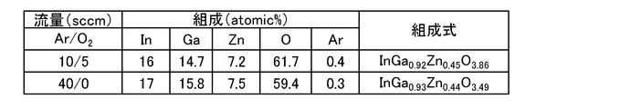
その後、上記の方法で作製した試料につき、誘導結合プラズマ質量分析法(Induct
ively Coupled Plasma Mass Spectrometry:I
CP-MS分析法)を用いて組成分析を行った。アルゴンガスの流量が10sccm、酸
素ガスの流量が5sccmの条件で得られる非単結晶半導体層102の組成は、InGa
0.94Zn0.40O3.31であった。上記分析結果と併せて、アルゴンガスの流量
が40sccm、酸素ガスの流量が0sccmの条件で作製した非単結晶半導体層の分析
結果を図2に示す。
After that, the sample prepared by the above method was subjected to inductively coupled plasma mass spectrometry (Induct
Ively Coupled Plasma Mass Spectrometry: I
A composition analysis was performed using CP-MS analysis method). The composition of the non-single-
0.94 Zn 0.40 O 3.31 . FIG. 2 shows the analysis results of the non-single-crystal semiconductor layers manufactured under the conditions of an argon gas flow rate of 40 sccm and an oxygen gas flow rate of 0 sccm, together with the above analysis results.
また、分析方法としてラザフォード後方散乱分析法(Rutherford Backs
cattering Spectrometry:RBS分析法)を用いた場合の結果を
図3に示す。
In addition, Rutherford backscattering analysis method as an analysis method (Rutherford Backs
FIG. 3 shows the results obtained by using cattering spectrometry (RBS analysis method).
図2及び図3から、非単結晶半導体層では、ターゲットの組成と比較して、Ga及びZn
の含有量が小さくなる傾向にあることが分かる。また、作製条件や分析方法等によって、
非単結晶半導体層の分析結果が異なっている。
2 and 3, in the non-single-crystal semiconductor layer, Ga and Zn
It can be seen that the content of In addition, depending on the production conditions and analysis method,
The analysis results of the non-single-crystal semiconductor layer are different.
次に、上記非単結晶半導体層に対して、350℃~800℃(好ましくは500~750
℃)で10分~200分程度の熱処理を施す。これにより、非晶質構造中に、結晶粒10
4を含む酸化物半導体層106が得られる(図1(b)参照)。上記酸化物半導体層10
6を用いて作製される薄膜トランジスタの電気特性は、ゲート電圧±20Vにおいて、オ
ンオフ比が109以上、移動度が10cm2/Vs以上と良好である。なお、ここでは、
700℃、1時間の条件で熱処理を行っている。
Next, the non-single-crystal semiconductor layer is heated to 350° C. to 800° C. (preferably 500 to 750° C.)
℃) for about 10 to 200 minutes. As a result, the
4 is obtained (see FIG. 1B). The
6, the on/off ratio is 10 9 or more and the mobility is 10 cm 2 /Vs or more at a gate voltage of ±20 V, which are excellent. In addition, here,
Heat treatment is performed at 700° C. for 1 hour.
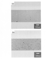
上記熱処理の後、酸化物半導体層106の構造を分析した。具体的には上記試料の断面に
つき、STEM(scanning transmission electron m
icroscope)像の観察を行った。
After the heat treatment, the structure of the
Microscope) images were observed.
図4に、上記試料のBright-field-STEM像を示す。図4(a)は、In
2O3:Ga2O3:ZnO=1:1:1(In:Ga:Zn=1:1:0.5)のター
ゲット(以下、ターゲットA)を用いて作製した試料のSTEM像であり、図4(b)は
、上記試料との比較のため、ターゲットのみをIn2O3:Ga2O3:ZnO=1:1
:2(In:Ga:Zn=1:1:1)(以下、ターゲットB)に変更して作製した試料
のSTEM像である。
FIG. 4 shows a Bright-field-STEM image of the above sample. FIG. 4(a) shows In
2 is a STEM image of a sample produced using a target (hereinafter referred to as target A) of 2 O 3 :Ga 2 O 3 :ZnO=1:1:1 (In:Ga:Zn=1:1:0.5). , and FIG. 4(b) shows only the target of In 2 O 3 :Ga 2 O 3 :ZnO=1:1 for comparison with the above sample.
: 2 (In:Ga:Zn=1:1:1) (hereinafter referred to as target B) is a STEM image of a sample fabricated.
図4から、上記の方法で作製した酸化物半導体層106は、非晶質構造中に結晶粒104
を含む構造を有していることが分かる。
From FIG. 4, the
It can be seen that it has a structure containing
なお、図4(a)と図4(b)との比較から分かるように、ターゲット中のZnの含有量
が少ない場合には、ターゲット中のZnの含有量が多い場合と比較して結晶成長の速度が
緩やかである。これを利用することにより、結晶成長の制御性を向上させることができる
。例えば、非単結晶半導体層102中のZnの含有量(原子%)を、Inの含有量(原子
%)未満かつGaの含有量(原子%)未満としてやれば、良好な酸化物半導体層106を
制御性良く形成することができる。一方で、結晶成長速度を重視する場合には、非単結晶
半導体層102中の亜鉛の含有量を増加させてやればよい。
As can be seen from the comparison between FIG. 4(a) and FIG. 4(b), when the Zn content in the target is low, the crystal growth is is slow. By utilizing this, the controllability of crystal growth can be improved. For example, if the Zn content (atomic %) in the non-single-
次に、より微細な領域のSTEM像観察を行った。図5に、ターゲットAを用いて作製し
た試料のSTEM像を示す。図5(a)がBright-field-STEM像、図5
(b)がHAADF(high-angle annular dark field)
-STEM像である。図5(a)からは規則的な構造が読み取れるが、各原子の位置を特
定する事は困難であり、結晶方位も判別できない。一方、図5(b)では、各原子に対応
する白い点の位置が明確に判別できる。また、図5(b)中の右下の領域には、非晶質構
造が残存していることが分かる。
Next, STEM image observation of a finer region was performed. FIG. 5 shows an STEM image of a sample produced using Target A. As shown in FIG. FIG. 5(a) is a Bright-field-STEM image, FIG.
(b) is HAADF (high-angle annular dark field)
- STEM images. Although a regular structure can be read from FIG. 5(a), it is difficult to specify the position of each atom, and the crystal orientation cannot be determined. On the other hand, in FIG. 5(b), the position of the white dot corresponding to each atom can be clearly identified. In addition, it can be seen that the amorphous structure remains in the lower right region in FIG. 5(b).
HAADF-STEM像においては、原子番号の2乗に比例したコントラストが得られる
ため、明るい点ほど重い原子を示すことになる。図5(b)においては明るい点がIn、
暗い点がGa又はZnである。
In the HAADF-STEM image, since the contrast is proportional to the square of the atomic number, the brighter the point, the heavier the atom. In FIG. 5(b), bright points are In,
Dark dots are Ga or Zn.
次に、図6を参照して、上記結晶構造についての考察を行う。ここで、図6中の左図(写
真)は、図5(b)の拡大図(拡大写真)である。また、図6中の右図は、InGaZn
O4(InGaO3(ZnO)mにおけるm=1に対応)を[100]方向から見た結晶
構造のモデル図である。図6中の左図と右図との対比により、ターゲットAを用いて作製
した試料における結晶粒は、InGaO3(ZnO)1の結晶構造を有していることが分
かる。なお、In-Ga-Zn-O系酸化物半導体においては、In及びGaが電気伝導
に寄与していると考えられるため、電気的特性を良好に保つためには、In及びGaの比
率が高い結晶構造、すなわち、InGaO3(ZnO)mにおいてm=1である結晶構造
の比率が高いほど好ましいといえる。
Next, with reference to FIG. 6, the above crystal structure will be considered. Here, the left figure (photograph) in FIG. 6 is an enlarged view (enlarged photograph) of FIG. 5(b). The right figure in FIG. 6 shows InGaZn
1 is a model diagram of the crystal structure of O 4 (corresponding to m=1 in InGaO 3 (ZnO) m ) viewed from the [100] direction. FIG. By comparing the left and right diagrams in FIG. 6, it can be seen that the crystal grains in the sample produced using the target A have the crystal structure of InGaO 3 (ZnO) 1 . In the In—Ga—Zn—O-based oxide semiconductor, In and Ga are considered to contribute to electrical conduction. It can be said that the higher the ratio of the crystal structure, that is, the crystal structure where m=1 in InGaO 3 (ZnO) m , the better.
図7に、ターゲットBを用いて作製した試料のHAADF-STEM像を示す。明るい点
が規則的に配列され、線状になっている様子が分かる。該明るい点によって形成される線
と線との間隔は、約0.9nm、約1.15nm、約1.4nmである。これは、それぞ
れ、m=1、m=2、m=3の結晶構造におけるインジウムの間隔に相当する。すなわち
、ターゲットBを用いて作製した試料においては、少なくともm=1~3までの複数の組
成の結晶を有しているといえる。
FIG. 7 shows an HAADF-STEM image of a sample produced using Target B. As shown in FIG. It can be seen that the bright dots are arranged regularly and form a line. The line-to-line spacings formed by the bright spots are about 0.9 nm, about 1.15 nm, and about 1.4 nm. This corresponds to the indium spacing in crystal structures with m=1, m=2 and m=3, respectively. In other words, it can be said that the sample produced using the target B has crystals with a plurality of compositions of at least m=1 to 3.
上述したように、In-Ga-Zn-O系酸化物半導体においてはIn及びGaが電気伝
導に寄与しているため、In及びGaの比率が低い状況(すなわち、mが大きい状況)で
は、その電気的特性は悪化する。そこで、m=1に係る構造の割合を高めておくことで、
電気的特性を良好に保つことが可能である。具体的には、m=1である結晶構造が、結晶
構造全体の80体積%以上を占めることが好ましい。より好ましくは90体積%以上であ
る。
As described above, in the In—Ga—Zn—O-based oxide semiconductor, In and Ga contribute to electrical conduction. Electrical properties deteriorate. Therefore, by increasing the ratio of the structure related to m = 1,
Good electrical characteristics can be maintained. Specifically, the crystal structure in which m=1 preferably occupies 80% by volume or more of the entire crystal structure. More preferably, it is 90% by volume or more.
m=1である結晶構造の割合を高める方法の一としては、Znの含有量が小さいターゲッ
トを用いて、Znの含有量が小さい非単結晶半導体層102を形成する方法がある。例え
ば、非単結晶半導体層102中のZnの含有量(原子%)を、Inの含有量(原子%)未
満かつGaの含有量(原子%)未満としてやれば良い。このように、非単結晶半導体層1
02中のZnの含有量を低減しておくことで、電気的に良好な特性の結晶構造を得ること
ができる。
As one method for increasing the proportion of the crystal structure in which m=1, there is a method of forming the non-single-
By reducing the Zn content in O2, a crystal structure with good electrical characteristics can be obtained.
In-Ga-Zn-O系酸化物半導体の電子状態は十分に解明されておらず、この電子状
態の解明が酸化物半導体の電気特性の理解へとつながるものと考えられる。そこで、以下
においては、In-Ga-Zn-O系酸化物半導体について行った第一原理計算の計算結
果及び考察を示す。なお、以下の計算結果は結晶構造に基づいて行ったものであるが、非
晶質構造中に結晶粒が含まれる構造においても同様に理解することができる。
The electronic state of the In—Ga—Zn—O-based oxide semiconductor has not been fully elucidated, and elucidation of the electronic state is believed to lead to understanding of the electrical characteristics of the oxide semiconductor. Therefore, calculation results and considerations of first-principles calculations performed on an In--Ga--Zn--O-based oxide semiconductor will be shown below. Although the following calculation results are based on the crystal structure, they can also be understood in the same way in a structure in which crystal grains are included in the amorphous structure.
図8に、計算によるIn-Ga-Zn-O系酸化物半導体(InGaZnO4)の結晶構
造を示す。InGaZnO4結晶構造の単位格子は21個の原子によって構成されるが、
ここではGaの配置を調べるため、84個の原子で構成される単位(2×2×1)にまで
拡張して計算を行った。
FIG. 8 shows a calculated crystal structure of an In--Ga--Zn--O-based oxide semiconductor ( InGaZnO.sub.4 ). The unit cell of the InGaZnO4 crystal structure is composed by 21 atoms,
Here, in order to investigate the arrangement of Ga, the calculation was extended to a unit (2×2×1) composed of 84 atoms.
計算は、CASTEPを用いて行っている。CASTEPは、密度汎関数理論(DFT)
と平面波-擬ポテンシャル法に基づいた第一原理計算プログラムである。ここでは交換相
関汎関数として、GGA(一般化勾配近似(generalized-gradient
approximation)及びPBE(Perdew-Burke-Ernzer
hof)を選択した。また、カットオフエネルギー(cut-off energy)を
500eV、k-pointを3×3×1とした。
Calculations are performed using CASTEP. CASTEP stands for Density Functional Theory (DFT)
and the plane wave-pseudopotential method. Here, as the exchange-correlation functional, GGA (generalized-gradient
approximation) and PBE (Perdew-Burke-Ernzer
hof) was selected. Also, the cut-off energy was set to 500 eV, and the k-point was set to 3×3×1.
図8から、単位格子は、2つの(Ga、Zn)O2レイヤーと1つのInO2レイヤーか
ら構成されていることが分かる。なお、ここでは簡単のため、所定の原子配置を有する単
位格子の繰り返しによる結晶構造を想定した。
From FIG. 8, it can be seen that the unit cell is composed of two (Ga, Zn)O 2 layers and one InO 2 layer. Here, for the sake of simplicity, the crystal structure is assumed to be a repetition of unit cells having a predetermined atomic arrangement.
図9に、単位格子中の2つの(Ga、Zn)O2レイヤーにおけるGa及びZnの配置を
示す。図9では、単位格子を2×2倍に拡張した構造を示している。また、図中の太線は
単位格子を示す。図9(a)は上部レイヤー(Upper Layer)及び下部レイヤ
ー(Lower Layer)にそれぞれ2つのGaが配置された場合を示しており、図
9(b)は上部レイヤーに一つのGaが配置され、下部レイヤーに3つのGaが配置され
た場合を示している。
Figure 9 shows the arrangement of Ga and Zn in two (Ga, Zn)O 2 layers in the unit cell. FIG. 9 shows a structure in which the unit cell is expanded 2×2 times. A thick line in the drawing indicates a unit cell. FIG. 9(a) shows the case where two Ga are arranged in the upper layer (Upper Layer) and the lower layer (Lower Layer) respectively, and FIG. 9(b) shows the case where one Ga is arranged in the upper layer, It shows the case where three Ga are arranged in the lower layer.
図9(a)に示す場合には、各レイヤー内におけるGaの配置は縞状となる。つまり、各
レイヤー内においてGaは互いに平行な線状の配置をとる。
In the case shown in FIG. 9A, Ga is arranged in stripes in each layer. In other words, Ga is linearly arranged in parallel to each other in each layer.
また、上部レイヤーと下部レイヤーの組み合わせを考えると、Gaの配置は平行配置と交
差配置の2つのパターンに分けられる。平行配置とは、上部レイヤーと下部レイヤーのG
aによるラインが互いに平行となる場合をいい、交差配置とは、上部レイヤーと下部レイ
ヤーのGaによるラインが交差する場合をいう。平行配置の場合には、例えば、U1+L
1やU1+L4のような2通りの組み合わせが考えられる。一方で、交差配置の場合には
、回転対称となるため、例えばU1+L2のような1通りの組み合わせが存在するに過ぎ
ない。つまり、図9(a)に示す場合には、計3通りの組み合わせがあるということにな
る。
Considering the combination of the upper layer and the lower layer, the arrangement of Ga can be divided into two patterns of parallel arrangement and cross arrangement. Parallel arrangement means G
The lines of a are parallel to each other, and the cross arrangement is the case of the Ga lines of the upper layer and the lower layer intersecting each other. In the case of parallel arrangement, for example U1+L
Two combinations such as 1 and U1+L4 are conceivable. On the other hand, in the case of the cross arrangement, there is only one combination such as U1+L2 because of rotational symmetry. That is, in the case shown in FIG. 9A, there are a total of three combinations.
図9(b)に示す場合、上部レイヤーと下部レイヤーの組み合わせとしては、例えばU7
+L7やU7+L10のような2通りが考えられる。なお、全てのGaが上部レイヤー又
は下部レイヤーのいずれか一方に入る場合、その組み合わせは1通りである(U11+L
11:図示せず)。よって、Gaの配置については計6通りの組み合わせを考えればよい
。
In the case shown in FIG. 9B, for example, U7 is a combination of the upper layer and the lower layer.
There are two possibilities such as +L7 and U7+L10. In addition, when all Ga is in either the upper layer or the lower layer, there is only one combination (U11+L
11: not shown). Therefore, a total of six combinations should be considered for the arrangement of Ga.
次に、上記の6通りの配置に関するエネルギーの比較結果を図10に示す。InGaZn
O4の最低エネルギーは、上部レイヤー及び下部レイヤーにそれぞれ2つのGaが配置さ
れる場合に現れる。より具体的には、U1+L1のような構造である。
Next, FIG. 10 shows the energy comparison results for the above six arrangements. InGaZn
The lowest energy of O 4 appears when two Ga are placed in the upper and lower layers, respectively. More specifically, it is a structure like U1+L1.
この構造(最低エネルギーとなる構造)に係る電子状態に関して、より詳細な計算を行っ
た。図11に、上記構造における電子のDOS(density of state)と
PDOS(projected density of state)の計算結果を示す
。図11より、Gaが最も支配的であり、次いでInの影響が大きいことが分かる。
A more detailed calculation was performed on the electronic state of this structure (the structure with the lowest energy). FIG. 11 shows the calculation results of the electronic DOS (density of state) and PDOS (projected density of state) in the above structure. From FIG. 11, it can be seen that Ga is the most dominant, followed by In.
次に、伝導帯の底の軌道関数Ψから、伝導帯の底における電子の存在確率|Ψ|2を計算
した。図12にその分布図を示す。ここで、図12(a)はIn面(InO2レイヤー中
)における電子の存在確率を表し、図12(b)は(Ga、Zn)O2レイヤーにおける
電子の存在確率を表している。Inの軌道が分離している点が興味深い。
Next, from the orbital function Ψ at the bottom of the conduction band, the existence probability |Ψ| FIG. 12 shows the distribution map. Here, FIG. 12(a) represents the electron existence probability on the In surface (in the InO 2 layer), and FIG. 12(b) represents the electron existence probability on the (Ga, Zn)O 2 layer. It is interesting that the orbitals of In are separated.
図12(b)から、Ga周辺では電子の存在確率が高く、Zn周辺では電子の存在確率が
低くなっていることが分かる。また、電気伝導のパスはIn面のみでなく、(Ga、Zn
)O2レイヤー中にも存在しているように見える。このことから、InGaZnO4の電
気伝導にはGaが大きく寄与しているものと考察される。Gaの軌道は、Inの軌道に作
用し、また、(Ga、Zn)O2レイヤーに係る電気伝導に寄与するようである。
From FIG. 12B, it can be seen that the existence probability of electrons is high around Ga, and the existence probability of electrons is low around Zn. In addition, the electric conduction path is not limited to the In surface, but also (Ga, Zn
) also appear to be present in the O2 layer. From this, it is considered that Ga greatly contributes to the electrical conduction of InGaZnO 4 . The Ga orbitals interact with the In orbitals and also appear to contribute to electrical conduction across the (Ga,Zn)O 2 layer.
InGaZnO4の特徴の一として、電気伝導率の許容度の高さが挙げられる。これは、
酸素空孔(欠陥)の発生確率に起因するものと思われる。プロセスにおいて加えられる酸
素の量によって電気伝導度が様々に変化するためである。そこで、このメカニズムを解明
すべく、酸素空孔の生成エネルギーを計算した。
One of the features of InGaZnO 4 is the high tolerance of electrical conductivity. this is,
This is thought to be due to the occurrence probability of oxygen vacancies (defects). This is because the electrical conductivity varies depending on the amount of oxygen added in the process. To elucidate this mechanism, we calculated the formation energy of oxygen vacancies.
なお、密度汎関数理論(DFT)に基づく計算においては、酸素空孔欠陥のエネルギー準
位は未だ議論の対象となっている。例えば、LDA(局所密度近似(Local den
sity approximation))やGGAのような関数によって得られるバン
ドギャップは、実測値より小さくなる傾向にある。このように、スケーリング法について
は未だ議論がなされているため、ここでは単純にスケーリング法無しのGGA関数を用い
ることとした。これにより、人為的な現象が除去されて、現象の本質を把握し得ると考え
られる。
In calculations based on density functional theory (DFT), the energy level of oxygen vacancy defects is still a subject of discussion. For example, LDA (Local Density Approximation)
The bandgap obtained by functions such as (sity approximation) and GGA tends to be smaller than the measured value. Since the scaling method is still being discussed in this way, the GGA function without the scaling method was simply used here. By doing so, it is thought that artificial phenomena can be removed and the essence of phenomena can be grasped.
酸素空孔のエネルギー(EVO)は次のように定義される。
EVO=E(AmOn―1)+E(O)-E(AmOn)
ここで、EVOは酸素分子のエネルギーの1/2であり、E(AmOn―1)は酸素空孔
を有するAmOn―1のエネルギーを意味する。Aは任意の元素を表している。
The oxygen vacancy energy (E VO ) is defined as follows.
EVO = E(A m O n-1 ) + E(O) - E(A m O n )
Here, E VO is half the energy of an oxygen molecule, and E(A m O n-1 ) means the energy of A m O n-1 having oxygen vacancies. A represents an arbitrary element.
図13に、酸素空孔を有する構造におけるEVOの幾何学的最適値の計算結果を示す。こ
こで、格子定数は理想的な結晶のものを用いた。EVOが高いということは、すなわち、
熱平衡状態における酸素空孔の密度が低いことを意味する。なお、図13においては、I
n2O3、ZnO、Ga2O3のEVOについても併せて示している。In2O3、Zn
O、Ga2O3の結晶構造はそれぞれ、ビックスバイト(bixbyte)型、ウルツ鉱
(wurtzite)型、β-Ga型である。
FIG. 13 shows the calculation results of the geometric optimum value of EVO in the structure with oxygen vacancies. Here, the lattice constant of an ideal crystal was used. High EVO means that
It means that the density of oxygen vacancies in the thermal equilibrium state is low. Note that in FIG.
EVO of n 2 O 3 , ZnO and Ga 2 O 3 are also shown. In2O3 , Zn
The crystal structures of O and Ga 2 O 3 are bixbyte type, wurtzite type and β-Ga type, respectively.
InGaZnO4におけるEVOは酸素空孔周辺の元素によって変化する。具体的には、
以下の3通りの構造モデルが考えられる。モデル1は、ある酸素空孔が、1個のZnと3
個のIn原子によって囲まれているモデルである。モデル2は、ある酸素空孔が、1個の
Gaと3個のIn原子によって囲まれているモデルである。モデル3は、ある酸素空孔が
、2個のZnと2個のGa原子によって囲まれているモデルである。図13からは、In
GaZnO4におけるEVOが、酸素空孔周辺のGa数の増加と共に増大することが読み
取れる。また、Ga2O3のEVOが最も大きくなっており、GaとOとは強固に結合し
ていると言える。
EVO in InGaZnO4 varies with the elements around the oxygen vacancies. In particular,
The following three structural models are conceivable.
The model is surrounded by 1 In atoms.
It can be seen that the EVO in GaZnO 4 increases with increasing Ga number around the oxygen vacancies. Moreover, the EVO of Ga 2 O 3 is the largest, and it can be said that Ga and O are strongly bonded.
InGaZnO4が非晶質の状態にある場合には、上記3通りのモデルに加え、より可能
性の高い構造が存在する。そして、各構造におけるEVOはわずかに異なる。InGaZ
nO4中のGaの割合が増大することにより、酸素空孔の密度は低下し、InGaZnO
4中のGaの割合が低下することにより、酸素空孔の密度は増大する。
In addition to the above three models, a more likely structure exists when InGaZnO 4 is in the amorphous state. And the EVO in each structure is slightly different. InGaZ
By increasing the proportion of Ga in nO , the density of oxygen vacancies decreases and InGaZnO
As the proportion of Ga in 4 decreases, the density of oxygen vacancies increases.
このように、非単結晶半導体層102中のGaの割合を高めることにより、酸素空孔の密
度を低減することができる。つまり、電気的特性の良好なIn-Ga-Zn-O系酸化物
半導体を得ることができる。電気伝導に寄与するInの存在を考えると、Inの割合を低
減することは好ましくないから、非単結晶半導体層102中のZnの割合を低くしてやる
ことが好ましい。例えば、非単結晶半導体層102中のZnの含有量(原子%)を、In
の含有量(原子%)未満かつGaの含有量(原子%)未満としてやれば良い。このように
、非単結晶半導体層102中のZnの含有量を低減しておくことで、電気的に良好な特性
の酸化物半導体層を得ることができる。
By increasing the proportion of Ga in the non-single-
is less than the content (atomic %) of Ga and less than the content (atomic %) of Ga. By reducing the Zn content in the non-single-
本実施の形態により、高性能な酸化物半導体層を提供することができる。なお、本実施の
形態は、他の実施の形態と適宜組み合わせて用いることができる。
According to this embodiment, a high-performance oxide semiconductor layer can be provided. Note that this embodiment can be used in appropriate combination with any of the other embodiments.
(実施の形態2)
本実施の形態では、実施の形態1において行ったIn-Ga-Zn-O系酸化物半導体層
に関する考察をさらに進めた結果について、図面を参照して説明する。
(Embodiment 2)
In this embodiment, results obtained by further studying the In--Ga--Zn--O-based oxide semiconductor layer in
実施の形態1において、InGaZnO4結晶構造の単位格子は、2つの(Ga、Zn)
O2レイヤーと1つのInO2レイヤーから構成されていることが示された。これを受け
、本実施の形態では、Ga及びZnの配置についてのより詳細な検討を行った。具体的に
は、図9に示したように上部レイヤーと下部レイヤーの組み合わせをいくつか考え、2つ
の(Ga、Zn)O2レイヤーにおけるGa及びZnの配置と、エネルギーとの関係につ
いて、計算及び考察を行った。
In
It was shown to consist of an O2 layer and one InO2 layer. In response to this, in the present embodiment, a more detailed study was conducted on the arrangement of Ga and Zn. Specifically, several combinations of the upper layer and the lower layer were considered as shown in FIG. I considered.
計算を行った具体的な組み合わせ(原子の配置)を図14に示す。本実施の形態において
は、最近接に係る同種原子の数に着目してこれらの組み合わせを選択した。例えば、図1
4(a)の組み合わせは、上部レイヤーと下部レイヤーにそれぞれGaとZnが分離して
配置されることにより、最近接に係る同種原子の数をゼロとしたものである。また、図1
4(b)の組み合わせは、最近接位置に同種原子が2個存在する場合であり、図14(c
)の組み合わせは、最近接位置に同種原子が1.5個存在する場合であり、図14(d)
の組み合わせは、最近接位置に同種原子が1個存在する場合である。計算条件は実施の形
態1において示したものと同じとした。
FIG. 14 shows specific combinations (arrangements of atoms) for which the calculation was performed. In the present embodiment, these combinations are selected by paying attention to the number of closest atoms of the same kind. For example, Figure 1
In the combination of 4(a), Ga and Zn are separately arranged in the upper layer and the lower layer, respectively, so that the number of closest homogeneous atoms is zero. Also, Figure 1
The combination of 4(b) is the case where two atoms of the same kind are present at the nearest position, and FIG. 14(c)
) is a case where 1.5 atoms of the same kind are present at the nearest position, and FIG. 14(d)
A combination of is a case where one atom of the same kind exists at the nearest position. The calculation conditions were the same as those shown in the first embodiment.
計算結果を図15に示す。図15では、最もエネルギーの低い構造を原点(エネルギーが
0eV)として、各構造のエネルギーを示している。
Calculation results are shown in FIG. FIG. 15 shows the energy of each structure with the structure with the lowest energy as the origin (energy is 0 eV).
本実施の形態において調査した配置は、多数の配置のうちのごく一部であるが、図15の
結果から、GaとZnの配置の傾向を読み取ることができる。図15の結果は、同種元素
の凝集度合が小さくなるに従って、エネルギー的に安定になる事を示すものと考えられる
。つまり、InGaZnO4結晶構造において、GaやZnは、GaOやZnOとして凝
集するのではなく、GaとZnが互いに混ざり合った配置を取ると結論できる。図16に
は、最も可能性が高い配置(図15(d)に対応)のモデル図を示す。
Although the arrangements investigated in this embodiment are only a part of many arrangements, the tendency of the arrangement of Ga and Zn can be read from the result of FIG. 15 . The results of FIG. 15 are considered to indicate that the smaller the degree of agglomeration of the same kind of elements, the more stable the energy becomes. In other words, it can be concluded that in the InGaZnO 4 crystal structure, Ga and Zn do not agglomerate as GaO or ZnO, but take a configuration in which Ga and Zn are mixed with each other. FIG. 16 shows a model diagram of the most probable arrangement (corresponding to FIG. 15(d)).
なお、本実施の形態は、他の実施の形態と適宜組み合わせて用いることができる。 Note that this embodiment can be used in appropriate combination with any of the other embodiments.
(実施の形態3)
本実施の形態では、実施の形態1などに示す方法を用いて作製した酸化物半導体層を用い
た半導体装置の作製工程の一例について、図17を参照して説明する。なお、本実施の形
態において、実施の形態1などと同様の内容についての詳細な説明は省略する。
(Embodiment 3)
In this embodiment, an example of a manufacturing process of a semiconductor device using an oxide semiconductor layer manufactured by the method described in
はじめに、絶縁表面を有する基板200上にゲート電極202を形成し、続いて当該ゲー
ト電極202上にゲート絶縁層204を形成した後、酸化物半導体層206と酸化物半導
体層207を積層して形成する(図17(a)参照)。
First, a
絶縁表面を有する基板200としては、例えば、液晶表示装置などに使用される可視光透
過性を有するガラス基板を用いることができる。上記のガラス基板は無アルカリガラス基
板であることが好ましい。無アルカリガラス基板には、例えば、アルミノシリケートガラ
ス、アルミノホウケイ酸ガラス、バリウムホウケイ酸ガラスなどのガラス材料が用いられ
ている。他にも、絶縁表面を有する基板200として、樹脂基板、セラミックス基板、石
英基板やサファイア基板などの絶縁体でなる絶縁性基板、珪素などの半導体材料でなる半
導体基板の表面を絶縁材料で被覆したもの、金属やステンレスなどの導電体でなる導電性
基板の表面を絶縁材料で被覆したもの、などを用いることができる。半導体装置の大面積
化という観点からは、特に、ガラス基板を用いることが好ましい。また、所定の耐熱性を
有していることが好ましい。
As the
ゲート電極202は、導電層を基板200全面に形成した後、フォトリソグラフィ法によ
り形成されたレジストマスクを用いて、該導電層を選択的にエッチングすることにより形
成することができる。この際、後に形成されるゲート絶縁層204の被覆性を向上し、段
切れを防止するために、ゲート電極202の端部がテーパー形状となるようエッチングす
ることが好ましい。なお、ゲート電極202にはゲート配線等、上記導電層によって形成
される電極や配線が含まれるものとする。
The
ゲート電極202は、アルミニウム(Al)や銅(Cu)などの低抵抗導電性材料で形成
することが望ましい。なお、配線及び電極としてアルミニウムを用いる場合、アルミニウ
ム単体では耐熱性が低く、腐蝕しやすい等の問題点があるため、耐熱性導電性材料と組み
合わせて形成することが好ましい。
The
上記の耐熱性導電性材料としては、チタン(Ti)、タンタル(Ta)、タングステン(
W)、モリブデン(Mo)、クロム(Cr)、Nd(ネオジム)、スカンジウム(Sc)
から選ばれた元素、または上述した元素を成分とする合金か、上述した元素を組み合わせ
た合金、または上述した元素を成分とする窒化物などを用いることができる。これらの耐
熱性導電性材料からなる膜とアルミニウム(又は銅)を積層させて、配線や電極を形成す
ることができる。
Examples of the above heat-resistant conductive materials include titanium (Ti), tantalum (Ta), tungsten (
W), molybdenum (Mo), chromium (Cr), Nd (neodymium), scandium (Sc)
or an alloy containing the above-described elements as a component, an alloy containing a combination of the above-described elements, or a nitride containing the above-described elements as a component can be used. Wirings and electrodes can be formed by laminating films made of these heat-resistant conductive materials and aluminum (or copper).
ゲート絶縁層204は、酸化シリコン膜、酸化窒化シリコン膜、窒化シリコン膜、窒化酸
化シリコン膜、酸化アルミニウム膜、酸化タンタル膜等で形成することができる。また、
これらの膜を積層させて設けてもよい。これらの膜は、スパッタ法等を用いて20nm以
上250nm以下の膜厚で形成することができる。例えば、ゲート絶縁層204として、
スパッタ法により酸化シリコン膜を100nmの厚さで形成する。なお、ゲート絶縁層2
04はトランジスタのゲート絶縁層として機能すればよく、作製方法や膜厚などについて
も上記の数値範囲に限定して解釈されるものではない。
The
These films may be laminated and provided. These films can be formed with a thickness of 20 nm or more and 250 nm or less using a sputtering method or the like. For example, as the
A silicon oxide film is formed with a thickness of 100 nm by a sputtering method. Note that the
04 should just function as a gate insulating layer of a transistor, and its manufacturing method and film thickness should not be construed as being limited to the above numerical ranges.
なお、ゲート絶縁層204上に酸化物半導体層206を形成する前に、ゲート絶縁層20
4の表面にプラズマ処理を行ってもよい。プラズマ処理を行うことにより、ゲート絶縁層
204の表面に付着しているゴミを除去することができる。
Note that the gate insulating layer 20 is formed before the
4 may be plasma-treated. By plasma treatment, dust attached to the surface of the
上記のプラズマ処理は、真空状態のチャンバーにアルゴン(Ar)ガス等の不活性ガスを
導入し、被処理物(ここでは、ゲート絶縁層204が形成された基板200)にバイアス
電圧を印加してプラズマ状態を形成することにより行うことができる。この場合、プラズ
マ中には電子とArの陽イオンが存在し、陰極方向(基板200側)にArの陽イオンが
加速される。加速されたArの陽イオンがゲート絶縁層204の表面に衝突することによ
って、当該ゲート絶縁層204の表面がスパッタエッチングされ、その表面を改質するこ
とができる。なお、アルゴンガスに代えて、ヘリウムガスを用いてもよい。また、アルゴ
ン雰囲気に酸素、水素、窒素等を加えた雰囲気で行ってもよい。また、アルゴン雰囲気に
塩素(Cl2)や四弗化炭素(CF4)などを加えた雰囲気で行ってもよい。このような
プラズマ処理を「逆スパッタ」と呼ぶこともある。
In the above plasma processing, an inert gas such as argon (Ar) gas is introduced into a chamber in a vacuum state, and a bias voltage is applied to the object to be processed (here, the
酸化物半導体層206は、In-Ga-Zn-O系非単結晶半導体層で形成することがで
きる。例えば、インジウム(In)、ガリウム(Ga)、及び亜鉛(Zn)を含む酸化物
半導体ターゲット(In2O3:Ga2O3:ZnO=1:1:1)を用いたスパッタ法
で、酸化物半導体層206を形成する。スパッタの条件等については実施の形態1などを
参照すればよい。
The
なお、上記スパッタにおいてパルス直流(DC)電源を用いると、ごみが軽減でき、膜厚
分布も均一となるため好ましい。また、上述したプラズマ処理を行った後、大気に曝すこ
となく酸化物半導体層206を形成することにより、ゲート絶縁層204と酸化物半導体
層206の界面にゴミや水分が付着することを抑制することができる。酸化物半導体層2
06の膜厚は、5nm~500nm程度とすればよい。
It is preferable to use a pulsed direct current (DC) power supply in the above sputtering, since dust can be reduced and the film thickness distribution can be uniform. By forming the
The film thickness of 06 may be about 5 nm to 500 nm.
酸化物半導体層207は、酸化物半導体層206と同様にIn-Ga-Zn-O系非単結
晶半導体層で形成することができる。例えば、In、Ga、及びZnを含む酸化物半導体
ターゲット(In2O3:Ga2O3:ZnO=1:1:1)を用いたスパッタ法で、酸
化物半導体層206上に酸化物半導体層207を形成することができる。この際に、酸化
物半導体層206を大気に曝すことなく酸化物半導体層207を連続して形成することが
好ましい。スパッタの条件は、例えば、温度を20℃~100℃、圧力を0.1Pa~2
.0Pa、電力を250W~3kW(8インチφ時)とすることができる。また、雰囲気
中にアルゴンガスを導入すると良い。
Like the
. 0 Pa and power of 250 W to 3 kW (at 8 inch diameter). Argon gas is preferably introduced into the atmosphere.
酸化物半導体層206と酸化物半導体層207の成膜条件は異ならせることが好ましい。
例えば、酸化物半導体層206の成膜条件においては、酸化物半導体層207の成膜条件
より、アルゴンガスの流量に対する酸素ガスの流量の比を大きくする。具体的には、酸化
物半導体層207の成膜条件は、希ガス(アルゴン、又はヘリウムなど)雰囲気下、また
は、酸素ガス10%以下、希ガス90%以上の雰囲気下とし、酸化物半導体層206の成
膜条件は、酸素雰囲気下、または、希ガスに対する酸素ガスの流量比が1以上の雰囲気下
とする。このようにすることで、酸化物半導体層206より電気伝導の高い酸化物半導体
層207を形成することができる。
The
For example, in the deposition conditions for the
酸化物半導体層206や酸化物半導体層207を形成する際のスパッタ法としては、スパ
ッタ用電源に高周波電源を用いるRFスパッタ法や、DCスパッタ法、パルス的に直流バ
イアスを加えるパルスDCスパッタ法などを用いることができる。
The sputtering method for forming the
また、材料の異なるターゲットを複数設置できる多元スパッタ装置を用いてもよい。多元
スパッタ装置では、同一チャンバーで異なる膜を積層形成することも、同一チャンバーで
複数種類の材料を同時にスパッタして一の膜を形成することもできる。さらに、チャンバ
ー内部に磁界発生機構を備えたマグネトロンスパッタ装置を用いる方法(マグネトロンス
パッタ法)や、マイクロ波を用いて発生させたプラズマを用いるECRスパッタ法等を用
いてもよい。また、成膜中にターゲット物質とスパッタガス成分とを化学反応させてそれ
らの化合物を形成するリアクティブスパッタ法や、成膜中に基板にも電圧をかけるバイア
ススパッタ法等を用いてもよい。
Alternatively, a multi-target sputtering apparatus capable of setting a plurality of targets made of different materials may be used. In the multi-source sputtering apparatus, different films can be laminated in the same chamber, and a single film can be formed by simultaneously sputtering a plurality of types of materials in the same chamber. Further, a method using a magnetron sputtering apparatus having a magnetic field generating mechanism inside a chamber (magnetron sputtering method), an ECR sputtering method using plasma generated using microwaves, or the like may be used. Alternatively, a reactive sputtering method in which a target material and a sputtering gas component are chemically reacted during film formation to form a compound thereof, or a bias sputtering method in which a voltage is applied to the substrate during film formation may also be used.
なお、本実施の形態では、酸化物半導体層206と酸化物半導体層207を積層させる場
合の一例について説明しているが、開示する発明はこれに限定されない。例えば、酸化物
半導体層207を設けない構成(酸化物半導体層206のみを形成する構成)としても良
い。
Note that although an example of stacking the
次に、酸化物半導体層207上にレジストマスク208を形成し、当該レジストマスク2
08を用いて酸化物半導体層206及び酸化物半導体層207を選択的にエッチングして
島状の酸化物半導体層210及び島状の酸化物半導体層211を形成する(図17(b)
参照)。
Next, a resist
08 to selectively etch the
reference).
上記のエッチングとしては、ウエットエッチングを用いると良い。例えば、ITO07N
(関東化学社製)、又は酢酸と硝酸と燐酸との混合液を用いたウエットエッチングにより
、酸化物半導体層206及び酸化物半導体層207の不要な部分を除去して、島状の酸化
物半導体層210及び島状の酸化物半導体層211を形成する。なお、上記エッチングの
後にはレジストマスク208は除去する。また、ウエットエッチングに用いるエッチャン
トは酸化物半導体層206及び酸化物半導体層207をエッチングできるものであればよ
く、上述したものに限られない。もちろん、上記のエッチングとしてドライエッチングを
用いても良い。
Wet etching is preferably used as the above etching. For example, ITO07N
(manufactured by Kanto Kagaku Co., Ltd.) or by wet etching using a mixture of acetic acid, nitric acid, and phosphoric acid, unnecessary portions of the
次に、島状の酸化物半導体層211上に導電層212を形成する(図17(c)参照)。
Next, a
導電層212は、スパッタ法や真空蒸着法等を用いて、アルミニウム(Al)、銅(Cu
)、チタン(Ti)、タンタル(Ta)、タングステン(W)、モリブデン(Mo)、ク
ロム(Cr)、Nd(ネオジム)、スカンジウム(Sc)から選ばれた元素を含む金属、
上述の元素を成分とする合金、上述した元素を組み合わせた合金、または、上述の元素を
成分とする窒化物等からなる材料で形成することができる。なお、本実施の形態において
は、導電層212の形成後に熱処理(例えば、350℃~800℃(好ましくは500~
750℃))を行うから、導電層212に所定の耐熱性を持たせることが好ましい。
The
), titanium (Ti), tantalum (Ta), tungsten (W), molybdenum (Mo), chromium (Cr), Nd (neodymium), a metal containing an element selected from scandium (Sc),
It can be formed of a material such as an alloy containing the above elements as a component, an alloy combining the above elements, or a nitride containing the above elements as a component. In this embodiment, heat treatment (for example, 350° C. to 800° C. (preferably 500° C. to
750° C.)), it is preferable that the
例えば、上記導電層212をチタン膜の単層構造で形成することができる。また、導電層
212を積層構造としても良く、例えば、アルミニウム膜とチタン膜との積層構造とする
ことができる。また、チタン膜と、ネオジムを含むアルミニウム(Al-Nd)膜と、チ
タン膜の3層構造としてもよい。さらに、導電層212を、シリコンを含むアルミニウム
膜の単層構造としてもよい。
For example, the
次に、導電層212上にレジストマスク214a、レジストマスク214b、レジストマ
スク214cを形成し、導電層212を選択的にエッチングして、導電層216a、導電
層216b、導電層218を形成すると共に、島状の酸化物半導体層211をエッチング
して導電率の高い半導体領域215a、導電率の高い半導体領域215bを形成し、島状
の酸化物半導体層210の一部(表面付近の一部)を除去(チャネルエッチ)する(図1
7(d)参照)。
Next, a resist
7(d)).
島状の酸化物半導体層210の一部、及び島状の酸化物半導体層211の一部が除去され
て形成される凹部220は、導電層216aと導電層216bの間、及び導電率の高い半
導体領域215aと導電率の高い半導体領域215bの間の領域にあたる。そのため、導
電層216aはトランジスタのソース電極又はドレイン電極の一方として機能し、導電層
216bはトランジスタのソース電極又はドレイン電極の他方として機能する。図17(
d)に示すように、酸化物半導体層210の一部、及び島状の酸化物半導体層211の一
部を除去して凹部220を形成することにより、導電層216aと導電層216bとの絶
縁を確実なものとすることができる。また、導電層218は、トランジスタ等を電気的に
接続する配線として機能する。
A recessed
As shown in d), part of the
上記のエッチングとしては、ドライエッチングを用いると良い。ドライエッチングを用い
ることで、ウエットエッチングを用いる場合と比較して配線構造などの微細化が可能とな
る。また、ドライエッチングを用いることにより、エッチングの制御性が良いため、島状
の酸化物半導体層210の除去(凹部220の形成)を制御性良く行うことができる。ド
ライエッチングに用いることができるガスとしては、塩素(Cl2)、塩化硼素(BCl
3)、塩化珪素(SiCl4)、四塩化炭素(CCl4)などの塩素系ガスや、四弗化炭
素(CF4)、弗化硫黄(SF6)、弗化窒素(NF3)、トリフルオロメタン(CHF
3)などのフッ素系ガス、臭化水素(HBr)、酸素(O2)、これらのガスにヘリウム
(He)やアルゴン(Ar)などの希ガスを添加したガス、などがある。もちろん、上記
エッチングとしてウエットエッチングを用いても良い。
Dry etching is preferably used as the above etching. By using dry etching, it is possible to miniaturize the wiring structure and the like compared to the case of using wet etching. In addition, since dry etching has good etching controllability, removal of the island-shaped oxide semiconductor layer 210 (formation of the recessed portion 220) can be performed with good controllability. Gases that can be used for dry etching include chlorine (Cl 2 ) and boron chloride (BCl).
3 ), chlorine-based gases such as silicon chloride (SiCl 4 ) and carbon tetrachloride (CCl 4 ), carbon tetrafluoride (CF 4 ), sulfur fluoride (SF 6 ), nitrogen fluoride (NF 3 ), trifluoride Romanethan (CHF)
3 ), hydrogen bromide (HBr), oxygen (O 2 ), and gases obtained by adding rare gases such as helium (He) and argon (Ar) to these gases. Of course, wet etching may be used as the etching.
また、導電層212の材料として、島状の酸化物半導体層210、又は島状の酸化物半導
体層211よりエッチングレートが高い材料を用いることが好ましい。これは、導電層2
12、島状の酸化物半導体層210、及び島状の酸化物半導体層211を一回でエッチン
グする場合、島状の酸化物半導体層210、又は島状の酸化物半導体層211のエッチン
グレートを導電層212のエッチングレートより小さくすることで、島状の酸化物半導体
層210が過度にエッチングされることを抑制することができるためである。
As a material for the
12. When the island-shaped
なお、上記エッチングの後にはレジストマスク214a、レジストマスク214b、レジ
ストマスク214cは除去する。
Note that the resist
その後、所定の温度条件(例えば、350℃~800℃(好ましくは500~750℃)
)で熱処理を行う。なお、絶縁表面を有する基板200としてガラス基板を用いる場合に
は、ガラス基板の歪み点以下の温度条件で熱処理を行う必要がある。熱処理の雰囲気は、
大気雰囲気や窒素雰囲気とすれば良い。この熱処理により、島状の酸化物半導体層210
中に酸化物半導体の結晶粒が成長し、InGaO3(ZnO)m(m>0)で表される非
晶質構造中に、InGaO3(ZnO)m(m=1)で表される結晶粒を含む酸化物半導
体層(In-Ga-Zn-O系酸化物半導体層)を得ることができる。
After that, predetermined temperature conditions (for example, 350 ° C. to 800 ° C. (preferably 500 to 750 ° C.)
) for heat treatment. Note that in the case where a glass substrate is used as the
An air atmosphere or a nitrogen atmosphere may be used. By this heat treatment, the island-shaped
A crystal grain of an oxide semiconductor grows inside, and a crystal represented by InGaO 3 (ZnO) m (m=1) is formed in an amorphous structure represented by InGaO 3 (ZnO) m (m>0). An oxide semiconductor layer (In--Ga--Zn--O-based oxide semiconductor layer) containing grains can be obtained.
なお、非晶質構造の酸化物半導体は熱などによって容易に結晶構造の酸化物半導体へと変
化するため、非晶質構造の比率が高い場合には、トランジスタの信頼性が低下する傾向に
ある。信頼性向上の観点からは、非晶質構造が90体積%以下(好ましくは80体積%以
下、より好ましくは60体積%以下)となるように熱処理を行う。
Note that an oxide semiconductor with an amorphous structure is easily changed to an oxide semiconductor with a crystalline structure by heat or the like; therefore, when the ratio of the amorphous structure is high, the reliability of the transistor tends to decrease. . From the viewpoint of improving reliability, the heat treatment is performed so that the amorphous structure is 90% by volume or less (preferably 80% by volume or less, more preferably 60% by volume or less).
熱処理の時間は熱処理の温度との関係で適宜変更することができるが、例えば、700℃
の温度条件においては、0.5~2時間程度とすればよい。また、熱処理に適した温度条
件は目的とする酸化物半導体の組成によって異なるから、所望の酸化物半導体層が得られ
る条件であれば特に限定されない。
The heat treatment time can be changed as appropriate in relation to the heat treatment temperature.
Under the temperature condition of , the time may be about 0.5 to 2 hours. In addition, temperature conditions suitable for heat treatment vary depending on the composition of the target oxide semiconductor, and thus are not particularly limited as long as the conditions are such that a desired oxide semiconductor layer can be obtained.
上記の熱処理は、拡散炉、抵抗加熱炉などの加熱炉、RTA(Rapid Therma
l Anneal)装置、マイクロ波加熱装置などを用いて行うことができる。酸化物半
導体に吸収される波長の光(電磁波)を照射することで熱処理に代えても良い。つまり、
光(電磁波)の照射によって、非晶質構造中に結晶粒を含む構造を実現しても良い。この
場合、光源としては、短波長を発振できるレーザー発振器や、紫外線ランプ等を用いれば
よい。
The above heat treatment may be performed in a diffusion furnace, a heating furnace such as a resistance heating furnace, an RTA (Rapid Therma
l Anneal) apparatus, microwave heating apparatus, or the like can be used. Heat treatment may be replaced by irradiation with light (electromagnetic waves) having a wavelength that can be absorbed by the oxide semiconductor. in short,
A structure including crystal grains in an amorphous structure may be realized by irradiation with light (electromagnetic waves). In this case, a laser oscillator capable of oscillating short wavelengths, an ultraviolet lamp, or the like may be used as the light source.
このように、InGaO3(ZnO)m(m>0)で表される非晶質構造中に、InGa
O3(ZnO)m(m=1)で表される結晶粒を含む酸化物半導体層をトランジスタのチ
ャネル形成領域として用いることで、高性能な半導体装置を提供することができる。
In this way, the InGa
By using an oxide semiconductor layer including crystal grains represented by O 3 (ZnO) m (m=1) as a channel formation region of a transistor, a high-performance semiconductor device can be provided.
ここで、電気的に良好な特性の酸化物半導体層を実現するためには、例えば、酸化物半導
体中のZnの含有量(原子%)を、Inの含有量(原子%)未満かつGaの含有量(原子
%)未満としてやることが好ましい。このような組成とすることにより、良好な特性を有
する酸化物半導体層を得ることができる。
Here, in order to realize an oxide semiconductor layer with good electrical characteristics, for example, the Zn content (atomic %) in the oxide semiconductor should be less than the In content (atomic %) and the Ga content should be less than the In content (atomic %). It is preferable to make it less than the content (atomic %). With such a composition, an oxide semiconductor layer having favorable characteristics can be obtained.
なお、上述のような、Znの含有量(原子%)がInの含有量(原子%)未満かつGaの
含有量(原子%)未満である酸化物半導体層は、目的とする組成に近いターゲットを用い
たスパッタリング法によって形成することができる。この場合、図2及び図3を考慮する
と、ターゲットの組成と比較して、形成された酸化物半導体層中におけるZnが低下する
割合はIn及びGaよりも大きいから、例えば、Znの含有量(原子%)が、Inの含有
量(原子%)未満かつGaの含有量(原子%)未満である酸化物半導体層を形成するため
には、Znの含有量(原子%)とIn又はGaの含有量(原子%)が等しいターゲットを
用いてもよい。つまり、ターゲットとしては、Znの含有量(原子%)がInの含有量(
原子%)以下かつGaの含有量(原子%)以下のものを用いればよい。
Note that the oxide semiconductor layer in which the Zn content (atomic %) is less than the In content (atomic %) and the Ga content (atomic %) is less than the target composition close to the target can be formed by a sputtering method using In this case, considering FIGS. 2 and 3, the rate at which Zn in the formed oxide semiconductor layer decreases is greater than that of In and Ga compared to the composition of the target. atomic %) is less than the In content (atomic %) and less than the Ga content (atomic %), the Zn content (atomic %) and the In or Ga Targets having the same content (atomic %) may be used. That is, as a target, the content of Zn (atomic %) is equal to the content of In (
atomic %) or less and the content of Ga (atomic %) or less may be used.
ここで、本実施の形態においては、上記熱処理を島状の酸化物半導体層210の形成後に
行う場合の一例について示しているが、熱処理を行うタイミングは、酸化物半導体層20
6の形成後であれば特に限定する必要はない。また、成膜の段階で非晶質構造中に複数の
結晶粒を含む構造(非晶質構造中に複数の結晶粒が分散された構造)が得られるのであれ
ば、熱処理は不要である。
Here, in this embodiment, an example in which the above heat treatment is performed after the island-shaped
There is no particular limitation as long as it is after the formation of 6 . Further, if a structure including a plurality of crystal grains in an amorphous structure (a structure in which a plurality of crystal grains are dispersed in the amorphous structure) can be obtained at the stage of film formation, heat treatment is unnecessary.
なお、露出している島状の酸化物半導体層210の凹部220に対しては、酸素ラジカル
処理を行ってもよい。酸素ラジカル処理を行うことにより島状の酸化物半導体層210を
チャネル形成領域とする薄膜トランジスタをノーマリーオフとすることが容易になる。ま
た、ラジカル処理を行うことにより、島状の酸化物半導体層210のエッチングによるダ
メージを回復することができる。ラジカル処理は、O2、N2O、酸素を含むN2、He
、Arなどの雰囲気下で行うことが好ましい。また、上記雰囲気にCl2、CF4を加え
た雰囲気下で行ってもよい。なお、ラジカル処理は、基板200側にバイアス電圧を印加
せずに行うことが好ましい。
Note that oxygen radical treatment may be performed on the exposed
, Ar, or the like. Alternatively, the above atmosphere may be added with Cl 2 or CF 4 . Note that the radical treatment is preferably performed without applying a bias voltage to the
次に、ゲート電極202、島状の酸化物半導体層210、導電率の高い半導体領域215
a、導電率の高い半導体領域215b、導電層216a、導電層216b等を含む薄膜ト
ランジスタ250を覆うように、保護絶縁層222を形成する(図17(e)参照)。保
護絶縁層222としては、スパッタ法などを用いて、窒化シリコン、酸化シリコン、窒化
酸化シリコン、酸化窒化シリコン、酸化アルミニウム、酸化タンタルなどの材料を含む層
を形成すればよい。
Next, the
a, a protective
その後、各種電極や配線を形成することで半導体装置が完成する。 After that, the semiconductor device is completed by forming various electrodes and wiring.
本実施の形態により、高性能な半導体装置を提供することができる。なお、本実施の形態
は、他の実施の形態と適宜組み合わせて用いることができる。
According to this embodiment mode, a high-performance semiconductor device can be provided. Note that this embodiment can be used in appropriate combination with any of the other embodiments.
100 基板
102 非単結晶半導体層
104 結晶粒
106 酸化物半導体層
200 基板
202 ゲート電極
204 ゲート絶縁層
206 酸化物半導体層
207 酸化物半導体層
208 レジストマスク
210 酸化物半導体層
211 酸化物半導体層
212 導電層
214a レジストマスク
214b レジストマスク
214c レジストマスク
215a 半導体領域
215b 半導体領域
216a 導電層
216b 導電層
218 導電層
220 凹部
222 保護絶縁層
250 薄膜トランジスタ
100
Claims (3)
前記第1の導電層の上面と接する領域と、前記第1の導電層の側面と接する領域と、を有する第1の絶縁層と、
前記第1の絶縁層の上面と接する領域を有する酸化物半導体層と、
前記酸化物半導体層と電気的に接続され、ソース電極又はドレイン電極としての機能を有する第2の導電層と、
前記トランジスタの断面視において、前記酸化物半導体層と前記第2の導電層との間に位置する第1の層と、を有し、
前記第1の層は、前記酸化物半導体層の上面と接する領域を有し、且つ前記酸化物半導体層の側面と接せず、
前記第2の導電層は、前記第1の絶縁層の上面と接する領域を有し、
前記酸化物半導体層及び前記第1の層は、それぞれInと、Gaと、Znと、を有し、
前記第1の層におけるZnの含有量は、前記酸化物半導体層におけるZnの含有量よりも大きく、
前記第1の層は、結晶構造を有し、且つ前記結晶構造の割合は、前記酸化物半導体層における結晶構造の割合と異なる、半導体装置。 a first conductive layer functioning as a gate electrode of a transistor;
a first insulating layer having a region in contact with the top surface of the first conductive layer and a region in contact with the side surface of the first conductive layer;
an oxide semiconductor layer having a region in contact with the top surface of the first insulating layer;
a second conductive layer electrically connected to the oxide semiconductor layer and functioning as a source electrode or a drain electrode;
a first layer positioned between the oxide semiconductor layer and the second conductive layer in a cross-sectional view of the transistor;
the first layer has a region in contact with the top surface of the oxide semiconductor layer and does not contact the side surface of the oxide semiconductor layer;
the second conductive layer has a region in contact with the top surface of the first insulating layer;
the oxide semiconductor layer and the first layer each contain In, Ga, and Zn ;
Zn content in the first layer is higher than Zn content in the oxide semiconductor layer ,
The semiconductor device, wherein the first layer has a crystal structure, and the ratio of the crystal structure is different from the ratio of the crystal structure in the oxide semiconductor layer .
前記第1の導電層の上面と接する領域と、前記第1の導電層の側面と接する領域と、を有する第1の絶縁層と、
前記第1の絶縁層の上面と接する領域を有する酸化物半導体層と、
前記酸化物半導体層と電気的に接続され、ソース電極又はドレイン電極としての機能を有する第2の導電層と、
前記トランジスタの断面視において、前記酸化物半導体層と前記第2の導電層との間に位置する第1の層と、を有し、
前記第1の層は、前記酸化物半導体層の上面と接する領域を有し、且つ前記酸化物半導体層の側面と接せず、
前記第2の導電層は、前記第1の絶縁層の上面と接する領域を有し、
前記酸化物半導体層及び前記第1の層は、それぞれInと、Gaと、Znと、を有し、
前記第1の層におけるZnの組成(原子%)は、前記酸化物半導体層におけるZnの組成(原子%)よりも大きく、
前記第1の層は、結晶構造を有し、且つ前記結晶構造の割合は、前記酸化物半導体層における結晶構造の割合と異なる、半導体装置。 a first conductive layer functioning as a gate electrode of a transistor;
a first insulating layer having a region in contact with the top surface of the first conductive layer and a region in contact with the side surface of the first conductive layer;
an oxide semiconductor layer having a region in contact with the top surface of the first insulating layer;
a second conductive layer electrically connected to the oxide semiconductor layer and functioning as a source electrode or a drain electrode;
a first layer positioned between the oxide semiconductor layer and the second conductive layer in a cross-sectional view of the transistor;
the first layer has a region in contact with the top surface of the oxide semiconductor layer and does not contact the side surface of the oxide semiconductor layer;
the second conductive layer has a region in contact with the top surface of the first insulating layer;
the oxide semiconductor layer and the first layer each contain In, Ga, and Zn ;
The Zn composition (atomic %) in the first layer is greater than the Zn composition (atomic %) in the oxide semiconductor layer,
The semiconductor device, wherein the first layer has a crystal structure, and the ratio of the crystal structure is different from the ratio of the crystal structure in the oxide semiconductor layer.
前記酸化物半導体層におけるZnの含有量は、前記酸化物半導体層におけるInの含有量未満であり、且つ前記酸化物半導体層におけるGaの含有量未満である、半導体装置。The semiconductor device, wherein the content of Zn in the oxide semiconductor layer is less than the content of In in the oxide semiconductor layer and less than the content of Ga in the oxide semiconductor layer.
Priority Applications (1)
| Application Number | Priority Date | Filing Date | Title |
|---|---|---|---|
| JP2022145742A JP2022172389A (en) | 2008-11-20 | 2022-09-14 | Semiconductor device |
Applications Claiming Priority (2)
| Application Number | Priority Date | Filing Date | Title |
|---|---|---|---|
| JP2008296901 | 2008-11-20 | ||
| JP2008296901 | 2008-11-20 |
Related Parent Applications (1)
| Application Number | Title | Priority Date | Filing Date |
|---|---|---|---|
| JP2019185631A Division JP6840816B2 (en) | 2008-11-20 | 2019-10-09 | Semiconductor device |
Related Child Applications (1)
| Application Number | Title | Priority Date | Filing Date |
|---|---|---|---|
| JP2022145742A Division JP2022172389A (en) | 2008-11-20 | 2022-09-14 | Semiconductor device |
Publications (2)
| Publication Number | Publication Date |
|---|---|
| JP2021073746A JP2021073746A (en) | 2021-05-13 |
| JP7143461B2 true JP7143461B2 (en) | 2022-09-28 |
Family
ID=42171261
Family Applications (8)
| Application Number | Title | Priority Date | Filing Date |
|---|---|---|---|
| JP2009251725A Withdrawn JP2010153802A (en) | 2008-11-20 | 2009-11-02 | Semiconductor device and method of manufacturing the same |
| JP2013192626A Expired - Fee Related JP5788942B2 (en) | 2008-11-20 | 2013-09-18 | Method for manufacturing semiconductor device |
| JP2015150837A Active JP6088599B2 (en) | 2008-11-20 | 2015-07-30 | Semiconductor device |
| JP2017018212A Expired - Fee Related JP6423463B2 (en) | 2008-11-20 | 2017-02-03 | Method for manufacturing transistor |
| JP2018167698A Active JP6602929B2 (en) | 2008-11-20 | 2018-09-07 | Transistor |
| JP2019185631A Active JP6840816B2 (en) | 2008-11-20 | 2019-10-09 | Semiconductor device |
| JP2021023311A Active JP7143461B2 (en) | 2008-11-20 | 2021-02-17 | semiconductor equipment |
| JP2022145742A Pending JP2022172389A (en) | 2008-11-20 | 2022-09-14 | Semiconductor device |
Family Applications Before (6)
| Application Number | Title | Priority Date | Filing Date |
|---|---|---|---|
| JP2009251725A Withdrawn JP2010153802A (en) | 2008-11-20 | 2009-11-02 | Semiconductor device and method of manufacturing the same |
| JP2013192626A Expired - Fee Related JP5788942B2 (en) | 2008-11-20 | 2013-09-18 | Method for manufacturing semiconductor device |
| JP2015150837A Active JP6088599B2 (en) | 2008-11-20 | 2015-07-30 | Semiconductor device |
| JP2017018212A Expired - Fee Related JP6423463B2 (en) | 2008-11-20 | 2017-02-03 | Method for manufacturing transistor |
| JP2018167698A Active JP6602929B2 (en) | 2008-11-20 | 2018-09-07 | Transistor |
| JP2019185631A Active JP6840816B2 (en) | 2008-11-20 | 2019-10-09 | Semiconductor device |
Family Applications After (1)
| Application Number | Title | Priority Date | Filing Date |
|---|---|---|---|
| JP2022145742A Pending JP2022172389A (en) | 2008-11-20 | 2022-09-14 | Semiconductor device |
Country Status (5)
| Country | Link |
|---|---|
| US (5) | US8329506B2 (en) |
| JP (8) | JP2010153802A (en) |
| KR (6) | KR20100056970A (en) |
| CN (2) | CN104409511B (en) |
| TW (5) | TWI585856B (en) |
Families Citing this family (72)
| Publication number | Priority date | Publication date | Assignee | Title |
|---|---|---|---|---|
| JPS6183684A (en) * | 1984-09-28 | 1986-04-28 | 株式会社日立製作所 | Method of bonding ceramic and metal |
| CN101719493B (en) | 2008-10-08 | 2014-05-14 | 株式会社半导体能源研究所 | Display device |
| JP2010153802A (en) * | 2008-11-20 | 2010-07-08 | Semiconductor Energy Lab Co Ltd | Semiconductor device and method of manufacturing the same |
| KR20170119742A (en) * | 2009-07-03 | 2017-10-27 | 가부시키가이샤 한도오따이 에네루기 켄큐쇼 | Method for manufacturing semiconductor device |
| KR102319490B1 (en) | 2009-07-10 | 2021-11-01 | 가부시키가이샤 한도오따이 에네루기 켄큐쇼 | Method for manufacturing liquid crystal display device |
| WO2011027723A1 (en) | 2009-09-04 | 2011-03-10 | Semiconductor Energy Laboratory Co., Ltd. | Semiconductor device and method for manufacturing the same |
| CN105428424A (en) * | 2009-09-16 | 2016-03-23 | 株式会社半导体能源研究所 | Transistor and display device |
| JP2011091386A (en) * | 2009-09-24 | 2011-05-06 | Semiconductor Energy Lab Co Ltd | Heat treatment apparatus, heat treatment method and method for manufacturing semiconductor device |
| KR102054650B1 (en) * | 2009-09-24 | 2019-12-11 | 가부시키가이샤 한도오따이 에네루기 켄큐쇼 | Oxide semiconductor film and semiconductor device |
| EP2486594B1 (en) * | 2009-10-08 | 2017-10-25 | Semiconductor Energy Laboratory Co., Ltd. | Oxide semiconductor device |
| KR102148664B1 (en) | 2009-11-06 | 2020-08-28 | 가부시키가이샤 한도오따이 에네루기 켄큐쇼 | Semiconductor device and manufacturing method thereof |
| KR101750982B1 (en) | 2009-11-06 | 2017-06-26 | 가부시키가이샤 한도오따이 에네루기 켄큐쇼 | Semiconductor device and manufacturing method thereof |
| WO2011068016A1 (en) * | 2009-12-04 | 2011-06-09 | Semiconductor Energy Laboratory Co., Ltd. | Semiconductor device |
| WO2011070900A1 (en) | 2009-12-08 | 2011-06-16 | Semiconductor Energy Laboratory Co., Ltd. | Semiconductor device and manufacturing method thereof |
| KR101768433B1 (en) * | 2009-12-18 | 2017-08-16 | 가부시키가이샤 한도오따이 에네루기 켄큐쇼 | Method for manufacturing semiconductor device |
| CN113540253A (en) | 2010-02-26 | 2021-10-22 | 株式会社半导体能源研究所 | Method for manufacturing semiconductor device |
| WO2011132625A1 (en) | 2010-04-23 | 2011-10-27 | Semiconductor Energy Laboratory Co., Ltd. | Manufacturing method of semiconductor device |
| US8785241B2 (en) | 2010-07-16 | 2014-07-22 | Semiconductor Energy Laboratory Co., Ltd. | Semiconductor device and manufacturing method thereof |
| TWI615920B (en) * | 2010-08-06 | 2018-02-21 | 半導體能源研究所股份有限公司 | Semiconductor device and method for manufacturing the same |
| TWI509707B (en) | 2010-08-16 | 2015-11-21 | Semiconductor Energy Lab | Manufacturing method of semiconductor device |
| JP5727892B2 (en) * | 2010-08-26 | 2015-06-03 | 株式会社半導体エネルギー研究所 | Semiconductor device |
| US8835917B2 (en) * | 2010-09-13 | 2014-09-16 | Semiconductor Energy Laboratory Co., Ltd. | Semiconductor device, power diode, and rectifier |
| US8664097B2 (en) | 2010-09-13 | 2014-03-04 | Semiconductor Energy Laboratory Co., Ltd. | Manufacturing method of semiconductor device |
| CN102455591A (en) | 2010-10-14 | 2012-05-16 | 京东方科技集团股份有限公司 | Manufacturing method for thin film pattern and array substrate |
| JP5666616B2 (en) * | 2010-10-25 | 2015-02-12 | 株式会社日立製作所 | Manufacturing method of oxide semiconductor device |
| JP5770068B2 (en) | 2010-11-12 | 2015-08-26 | 株式会社半導体エネルギー研究所 | Semiconductor device |
| US8809852B2 (en) | 2010-11-30 | 2014-08-19 | Semiconductor Energy Laboratory Co., Ltd. | Semiconductor film, semiconductor element, semiconductor device, and method for manufacturing the same |
| US8823092B2 (en) | 2010-11-30 | 2014-09-02 | Semiconductor Energy Laboratory Co., Ltd. | Semiconductor device and manufacturing method thereof |
| TWI562379B (en) | 2010-11-30 | 2016-12-11 | Semiconductor Energy Lab Co Ltd | Semiconductor device and method for manufacturing semiconductor device |
| US8629496B2 (en) | 2010-11-30 | 2014-01-14 | Semiconductor Energy Laboratory Co., Ltd. | Semiconductor device and method for manufacturing the same |
| KR102110496B1 (en) | 2010-12-03 | 2020-05-13 | 가부시키가이샤 한도오따이 에네루기 켄큐쇼 | Oxide semiconductor film and semiconductor device |
| KR102424181B1 (en) | 2010-12-17 | 2022-07-21 | 가부시키가이샤 한도오따이 에네루기 켄큐쇼 | Oxide material and semiconductor device |
| WO2012090973A1 (en) * | 2010-12-28 | 2012-07-05 | Semiconductor Energy Laboratory Co., Ltd. | Semiconductor device and manufacturing method thereof |
| WO2012090799A1 (en) * | 2010-12-28 | 2012-07-05 | Semiconductor Energy Laboratory Co., Ltd. | Semiconductor device and method for manufacturing the same |
| JP5897910B2 (en) | 2011-01-20 | 2016-04-06 | 株式会社半導体エネルギー研究所 | Method for manufacturing semiconductor device |
| TWI570920B (en) * | 2011-01-26 | 2017-02-11 | 半導體能源研究所股份有限公司 | Semiconductor device and manufacturing method thereof |
| JP2012169344A (en) * | 2011-02-10 | 2012-09-06 | Sony Corp | Thin film transistor, display device and electronic equipment |
| US9478668B2 (en) * | 2011-04-13 | 2016-10-25 | Semiconductor Energy Laboratory Co., Ltd. | Oxide semiconductor film and semiconductor device |
| US20120298998A1 (en) | 2011-05-25 | 2012-11-29 | Semiconductor Energy Laboratory Co., Ltd. | Method for forming oxide semiconductor film, semiconductor device, and method for manufacturing semiconductor device |
| US8514626B2 (en) * | 2011-07-26 | 2013-08-20 | Micron Technology, Inc. | Memory cells and methods of storing information |
| JP6006572B2 (en) * | 2011-08-18 | 2016-10-12 | 株式会社半導体エネルギー研究所 | Semiconductor device |
| KR102128369B1 (en) | 2011-09-29 | 2020-06-30 | 가부시키가이샤 한도오따이 에네루기 켄큐쇼 | Semiconductor device |
| KR20130040706A (en) | 2011-10-14 | 2013-04-24 | 가부시키가이샤 한도오따이 에네루기 켄큐쇼 | Semiconductor device and method of manufacturing semiconductor device |
| DE112012004307B4 (en) | 2011-10-14 | 2017-04-13 | Semiconductor Energy Laboratory Co., Ltd. | Semiconductor device |
| KR101976212B1 (en) * | 2011-10-24 | 2019-05-07 | 가부시키가이샤 한도오따이 에네루기 켄큐쇼 | Semiconductor device and method for manufacturing the same |
| US9057126B2 (en) * | 2011-11-29 | 2015-06-16 | Semiconductor Energy Laboratory Co., Ltd. | Method for manufacturing sputtering target and method for manufacturing semiconductor device |
| TW201405828A (en) * | 2012-07-31 | 2014-02-01 | E Ink Holdings Inc | Display panel, thin film transistor and method of fabricating the same |
| JP6284710B2 (en) * | 2012-10-18 | 2018-02-28 | 出光興産株式会社 | Sputtering target, oxide semiconductor thin film, and manufacturing method thereof |
| TWI527230B (en) * | 2012-10-19 | 2016-03-21 | 元太科技工業股份有限公司 | Thin film transistor structure and method for manufacturing the same |
| CN109065553A (en) | 2012-11-08 | 2018-12-21 | 株式会社半导体能源研究所 | The forming method of metal oxide film and metal oxide film |
| US9246011B2 (en) * | 2012-11-30 | 2016-01-26 | Semiconductor Energy Laboratory Co., Ltd. | Semiconductor device |
| US9153650B2 (en) | 2013-03-19 | 2015-10-06 | Semiconductor Energy Laboratory Co., Ltd. | Oxide semiconductor |
| TWI608523B (en) * | 2013-07-19 | 2017-12-11 | 半導體能源研究所股份有限公司 | Oxide semiconductor film, method of manufacturing oxide semiconductor film, and semiconductor device |
| US20150034475A1 (en) * | 2013-08-02 | 2015-02-05 | Semiconductor Energy Laboratory Co., Ltd. | Method for forming oxide semiconductor film |
| WO2015125042A1 (en) * | 2014-02-19 | 2015-08-27 | Semiconductor Energy Laboratory Co., Ltd. | Oxide, semiconductor device, module, and electronic device |
| WO2015132697A1 (en) | 2014-03-07 | 2015-09-11 | Semiconductor Energy Laboratory Co., Ltd. | Semiconductor device |
| TWI669761B (en) * | 2014-05-30 | 2019-08-21 | 日商半導體能源研究所股份有限公司 | Semiconductor device and display device including the same |
| TWI666776B (en) | 2014-06-20 | 2019-07-21 | 日商半導體能源研究所股份有限公司 | Semiconductor device and display device having the same |
| JPWO2016084636A1 (en) * | 2014-11-25 | 2017-10-12 | 住友金属鉱山株式会社 | Oxide sintered body, sputtering target, and oxide semiconductor thin film obtained using the same |
| JP6796086B2 (en) * | 2016-02-05 | 2020-12-02 | 株式会社半導体エネルギー研究所 | Semiconductor device |
| US10388738B2 (en) * | 2016-04-01 | 2019-08-20 | Semiconductor Energy Laboratory Co., Ltd. | Composite oxide semiconductor and method for manufacturing the same |
| WO2017168283A1 (en) | 2016-04-01 | 2017-10-05 | 株式会社半導体エネルギー研究所 | Composite oxide semiconductor, semiconductor device using said composite oxide semiconductor, and display device having said semiconductor device |
| KR102492209B1 (en) | 2016-05-19 | 2023-01-27 | 가부시키가이샤 한도오따이 에네루기 켄큐쇼 | Composite oxide semiconductor and transistor |
| WO2017208119A1 (en) | 2016-06-03 | 2017-12-07 | Semiconductor Energy Laboratory Co., Ltd. | Metal oxide and field-effect transistor |
| WO2017208109A1 (en) | 2016-06-03 | 2017-12-07 | Semiconductor Energy Laboratory Co., Ltd. | Sputtering target, oxide semiconductor, oxynitride semiconductor, and transistor |
| JP6800092B2 (en) * | 2016-06-24 | 2020-12-16 | 株式会社半導体エネルギー研究所 | Transistors and display devices |
| TW202224189A (en) * | 2016-10-21 | 2022-06-16 | 日商半導體能源研究所股份有限公司 | Composite oxide semiconductor and transistor |
| JP6392955B2 (en) * | 2017-08-24 | 2018-09-19 | 株式会社半導体エネルギー研究所 | Metal oxide film |
| CN107946365A (en) * | 2017-10-24 | 2018-04-20 | 华南理工大学 | A kind of inorganic, metal oxide film and its manufacture method with compound crystal form |
| JP6553266B2 (en) * | 2018-08-23 | 2019-07-31 | 株式会社半導体エネルギー研究所 | Metal oxide film and semiconductor device |
| JP6733015B2 (en) * | 2019-07-03 | 2020-07-29 | 株式会社半導体エネルギー研究所 | Metal oxide film and semiconductor device |
| JP6999754B2 (en) * | 2020-07-08 | 2022-01-19 | 株式会社半導体エネルギー研究所 | Semiconductor device |
Citations (3)
| Publication number | Priority date | Publication date | Assignee | Title |
|---|---|---|---|---|
| JP2005285890A (en) | 2004-03-29 | 2005-10-13 | Casio Comput Co Ltd | Zinc oxide processing method |
| JP2007150158A (en) | 2005-11-30 | 2007-06-14 | Toppan Printing Co Ltd | Transistor and its manufacturing method |
| JP2007173489A (en) | 2005-12-21 | 2007-07-05 | Idemitsu Kosan Co Ltd | Tft substrate and method of manufacturing the same |
Family Cites Families (147)
| Publication number | Priority date | Publication date | Assignee | Title |
|---|---|---|---|---|
| JPS60198861A (en) | 1984-03-23 | 1985-10-08 | Fujitsu Ltd | Thin film transistor |
| JPH0244256B2 (en) | 1987-01-28 | 1990-10-03 | Kagaku Gijutsucho Mukizaishitsu Kenkyushocho | INGAZN2O5DESHIMESARERUROTSUHOSHOKEINOSOJOKOZOOJUSURUKAGOBUTSUOYOBISONOSEIZOHO |
| JPH0244258B2 (en) | 1987-02-24 | 1990-10-03 | Kagaku Gijutsucho Mukizaishitsu Kenkyushocho | INGAZN3O6DESHIMESARERUROTSUHOSHOKEINOSOJOKOZOOJUSURUKAGOBUTSUOYOBISONOSEIZOHO |
| JPH0244260B2 (en) | 1987-02-24 | 1990-10-03 | Kagaku Gijutsucho Mukizaishitsu Kenkyushocho | INGAZN5O8DESHIMESARERUROTSUHOSHOKEINOSOJOKOZOOJUSURUKAGOBUTSUOYOBISONOSEIZOHO |
| JPS63210023A (en) | 1987-02-24 | 1988-08-31 | Natl Inst For Res In Inorg Mater | Compound having laminar structure of hexagonal crystal system expressed by ingazn4o7 and its production |
| JPH0244262B2 (en) | 1987-02-27 | 1990-10-03 | Kagaku Gijutsucho Mukizaishitsu Kenkyushocho | INGAZN6O9DESHIMESARERUROTSUHOSHOKEINOSOJOKOZOOJUSURUKAGOBUTSUOYOBISONOSEIZOHO |
| JPH0244263B2 (en) | 1987-04-22 | 1990-10-03 | Kagaku Gijutsucho Mukizaishitsu Kenkyushocho | INGAZN7O10DESHIMESARERUROTSUHOSHOKEINOSOJOKOZOOJUSURUKAGOBUTSUOYOBISONOSEIZOHO |
| EP0445535B1 (en) * | 1990-02-06 | 1995-02-01 | Sel Semiconductor Energy Laboratory Co., Ltd. | Method of forming an oxide film |
| JP2585118B2 (en) | 1990-02-06 | 1997-02-26 | 株式会社半導体エネルギー研究所 | Method for manufacturing thin film transistor |
| JPH05251705A (en) | 1992-03-04 | 1993-09-28 | Fuji Xerox Co Ltd | Thin-film transistor |
| JP3179287B2 (en) | 1993-12-28 | 2001-06-25 | 出光興産株式会社 | Conductive transparent substrate and method for producing the same |
| JP3479375B2 (en) | 1995-03-27 | 2003-12-15 | 科学技術振興事業団 | Metal oxide semiconductor device in which a pn junction is formed with a thin film transistor made of a metal oxide semiconductor such as cuprous oxide, and methods for manufacturing the same |
| EP0820644B1 (en) * | 1995-08-03 | 2005-08-24 | Koninklijke Philips Electronics N.V. | Semiconductor device provided with transparent switching element |
| US5847410A (en) | 1995-11-24 | 1998-12-08 | Semiconductor Energy Laboratory Co. | Semiconductor electro-optical device |
| JP3625598B2 (en) * | 1995-12-30 | 2005-03-02 | 三星電子株式会社 | Manufacturing method of liquid crystal display device |
| US6323317B1 (en) * | 1996-11-01 | 2001-11-27 | The Walter And Eliza Hall Institute Of Medical Research | Therapeutic and diagnostics proteins comprising a SOCS box |
| JP2000026119A (en) * | 1998-07-09 | 2000-01-25 | Hoya Corp | Article having transparent electrically conductive oxide thin film and its manufacture |
| JP4170454B2 (en) | 1998-07-24 | 2008-10-22 | Hoya株式会社 | Article having transparent conductive oxide thin film and method for producing the same |
| JP2000150861A (en) * | 1998-11-16 | 2000-05-30 | Tdk Corp | Oxide thin film |
| JP3276930B2 (en) | 1998-11-17 | 2002-04-22 | 科学技術振興事業団 | Transistor and semiconductor device |
| TW460731B (en) * | 1999-09-03 | 2001-10-21 | Ind Tech Res Inst | Electrode structure and production method of wide viewing angle LCD |
| JP4089858B2 (en) | 2000-09-01 | 2008-05-28 | 国立大学法人東北大学 | Semiconductor device |
| KR20020038482A (en) * | 2000-11-15 | 2002-05-23 | 모리시타 요이찌 | Thin film transistor array, method for producing the same, and display panel using the same |
| JP3997731B2 (en) * | 2001-03-19 | 2007-10-24 | 富士ゼロックス株式会社 | Method for forming a crystalline semiconductor thin film on a substrate |
| JP2002289859A (en) | 2001-03-23 | 2002-10-04 | Minolta Co Ltd | Thin-film transistor |
| JP4090716B2 (en) | 2001-09-10 | 2008-05-28 | 雅司 川崎 | Thin film transistor and matrix display device |
| JP3925839B2 (en) | 2001-09-10 | 2007-06-06 | シャープ株式会社 | Semiconductor memory device and test method thereof |
| JP4164562B2 (en) | 2002-09-11 | 2008-10-15 | 独立行政法人科学技術振興機構 | Transparent thin film field effect transistor using homologous thin film as active layer |
| WO2003040441A1 (en) * | 2001-11-05 | 2003-05-15 | Japan Science And Technology Agency | Natural superlattice homologous single crystal thin film, method for preparation thereof, and device using said single crystal thin film |
| JP4083486B2 (en) * | 2002-02-21 | 2008-04-30 | 独立行政法人科学技術振興機構 | Method for producing LnCuO (S, Se, Te) single crystal thin film |
| US7049190B2 (en) * | 2002-03-15 | 2006-05-23 | Sanyo Electric Co., Ltd. | Method for forming ZnO film, method for forming ZnO semiconductor layer, method for fabricating semiconductor device, and semiconductor device |
| JP3933591B2 (en) * | 2002-03-26 | 2007-06-20 | 淳二 城戸 | Organic electroluminescent device |
| US7339187B2 (en) * | 2002-05-21 | 2008-03-04 | State Of Oregon Acting By And Through The Oregon State Board Of Higher Education On Behalf Of Oregon State University | Transistor structures |
| JP2004022625A (en) * | 2002-06-13 | 2004-01-22 | Murata Mfg Co Ltd | Manufacturing method of semiconductor device and its manufacturing method |
| US7105868B2 (en) * | 2002-06-24 | 2006-09-12 | Cermet, Inc. | High-electron mobility transistor with zinc oxide |
| US7067843B2 (en) * | 2002-10-11 | 2006-06-27 | E. I. Du Pont De Nemours And Company | Transparent oxide semiconductor thin film transistors |
| JP4166105B2 (en) | 2003-03-06 | 2008-10-15 | シャープ株式会社 | Semiconductor device and manufacturing method thereof |
| JP2004273732A (en) | 2003-03-07 | 2004-09-30 | Sharp Corp | Active matrix substrate and its producing process |
| JP4108633B2 (en) | 2003-06-20 | 2008-06-25 | シャープ株式会社 | THIN FILM TRANSISTOR, MANUFACTURING METHOD THEREOF, AND ELECTRONIC DEVICE |
| US7262463B2 (en) * | 2003-07-25 | 2007-08-28 | Hewlett-Packard Development Company, L.P. | Transistor including a deposited channel region having a doped portion |
| JP2005129666A (en) * | 2003-10-22 | 2005-05-19 | Canon Inc | Treatment method and apparatus |
| US7282782B2 (en) | 2004-03-12 | 2007-10-16 | Hewlett-Packard Development Company, L.P. | Combined binary oxide semiconductor device |
| US7145174B2 (en) * | 2004-03-12 | 2006-12-05 | Hewlett-Packard Development Company, Lp. | Semiconductor device |
| US7297977B2 (en) * | 2004-03-12 | 2007-11-20 | Hewlett-Packard Development Company, L.P. | Semiconductor device |
| KR101078483B1 (en) | 2004-03-12 | 2011-10-31 | 도꾸리쯔교세이호징 가가꾸 기쥬쯔 신꼬 기꼬 | Switching device of lcd or organic electro luminescence display |
| US7211825B2 (en) * | 2004-06-14 | 2007-05-01 | Yi-Chi Shih | Indium oxide-based thin film transistors and circuits |
| JP2006100760A (en) * | 2004-09-02 | 2006-04-13 | Casio Comput Co Ltd | Thin-film transistor and its manufacturing method |
| US7285501B2 (en) * | 2004-09-17 | 2007-10-23 | Hewlett-Packard Development Company, L.P. | Method of forming a solution processed device |
| US7298084B2 (en) * | 2004-11-02 | 2007-11-20 | 3M Innovative Properties Company | Methods and displays utilizing integrated zinc oxide row and column drivers in conjunction with organic light emitting diodes |
| US7453065B2 (en) * | 2004-11-10 | 2008-11-18 | Canon Kabushiki Kaisha | Sensor and image pickup device |
| US7863611B2 (en) * | 2004-11-10 | 2011-01-04 | Canon Kabushiki Kaisha | Integrated circuits utilizing amorphous oxides |
| US7829444B2 (en) * | 2004-11-10 | 2010-11-09 | Canon Kabushiki Kaisha | Field effect transistor manufacturing method |
| JP5138163B2 (en) * | 2004-11-10 | 2013-02-06 | キヤノン株式会社 | Field effect transistor |
| EP1810335B1 (en) * | 2004-11-10 | 2020-05-27 | Canon Kabushiki Kaisha | Light-emitting device |
| EP2455975B1 (en) | 2004-11-10 | 2015-10-28 | Canon Kabushiki Kaisha | Field effect transistor with amorphous oxide |
| US7868326B2 (en) * | 2004-11-10 | 2011-01-11 | Canon Kabushiki Kaisha | Field effect transistor |
| US7791072B2 (en) * | 2004-11-10 | 2010-09-07 | Canon Kabushiki Kaisha | Display |
| US7579224B2 (en) * | 2005-01-21 | 2009-08-25 | Semiconductor Energy Laboratory Co., Ltd. | Method for manufacturing a thin film semiconductor device |
| TWI412138B (en) * | 2005-01-28 | 2013-10-11 | Semiconductor Energy Lab | Semiconductor device, electronic device, and method of manufacturing semiconductor device |
| TWI445178B (en) * | 2005-01-28 | 2014-07-11 | Semiconductor Energy Lab | Semiconductor device, electronic device, and method of manufacturing semiconductor device |
| US7858451B2 (en) * | 2005-02-03 | 2010-12-28 | Semiconductor Energy Laboratory Co., Ltd. | Electronic device, semiconductor device and manufacturing method thereof |
| US7948171B2 (en) * | 2005-02-18 | 2011-05-24 | Semiconductor Energy Laboratory Co., Ltd. | Light emitting device |
| US20060197092A1 (en) * | 2005-03-03 | 2006-09-07 | Randy Hoffman | System and method for forming conductive material on a substrate |
| US8681077B2 (en) * | 2005-03-18 | 2014-03-25 | Semiconductor Energy Laboratory Co., Ltd. | Semiconductor device, and display device, driving method and electronic apparatus thereof |
| WO2006105077A2 (en) * | 2005-03-28 | 2006-10-05 | Massachusetts Institute Of Technology | Low voltage thin film transistor with high-k dielectric material |
| US20060228898A1 (en) | 2005-03-30 | 2006-10-12 | Cory Wajda | Method and system for forming a high-k dielectric layer |
| US7645478B2 (en) * | 2005-03-31 | 2010-01-12 | 3M Innovative Properties Company | Methods of making displays |
| US8300031B2 (en) * | 2005-04-20 | 2012-10-30 | Semiconductor Energy Laboratory Co., Ltd. | Semiconductor device comprising transistor having gate and drain connected through a current-voltage conversion element |
| JP2006344849A (en) | 2005-06-10 | 2006-12-21 | Casio Comput Co Ltd | Thin film transistor |
| US7402506B2 (en) * | 2005-06-16 | 2008-07-22 | Eastman Kodak Company | Methods of making thin film transistors comprising zinc-oxide-based semiconductor materials and transistors made thereby |
| US7691666B2 (en) | 2005-06-16 | 2010-04-06 | Eastman Kodak Company | Methods of making thin film transistors comprising zinc-oxide-based semiconductor materials and transistors made thereby |
| US7507618B2 (en) | 2005-06-27 | 2009-03-24 | 3M Innovative Properties Company | Method for making electronic devices using metal oxide nanoparticles |
| KR100711890B1 (en) * | 2005-07-28 | 2007-04-25 | 삼성에스디아이 주식회사 | Organic Light Emitting Display and Fabrication Method for the same |
| US7683370B2 (en) * | 2005-08-17 | 2010-03-23 | Kobe Steel, Ltd. | Source/drain electrodes, transistor substrates and manufacture methods, thereof, and display devices |
| JP2007059128A (en) * | 2005-08-23 | 2007-03-08 | Canon Inc | Organic electroluminescent display device and manufacturing method thereof |
| JP4870403B2 (en) * | 2005-09-02 | 2012-02-08 | 財団法人高知県産業振興センター | Thin film transistor manufacturing method |
| JP5058469B2 (en) * | 2005-09-06 | 2012-10-24 | キヤノン株式会社 | Sputtering target and method for forming a thin film using the target |
| JP2007073705A (en) * | 2005-09-06 | 2007-03-22 | Canon Inc | Oxide-semiconductor channel film transistor and its method of manufacturing same |
| JP5116225B2 (en) * | 2005-09-06 | 2013-01-09 | キヤノン株式会社 | Manufacturing method of oxide semiconductor device |
| JP4850457B2 (en) * | 2005-09-06 | 2012-01-11 | キヤノン株式会社 | Thin film transistor and thin film diode |
| JP4280736B2 (en) * | 2005-09-06 | 2009-06-17 | キヤノン株式会社 | Semiconductor element |
| JP5078246B2 (en) | 2005-09-29 | 2012-11-21 | 株式会社半導体エネルギー研究所 | Semiconductor device and manufacturing method of semiconductor device |
| JP5064747B2 (en) * | 2005-09-29 | 2012-10-31 | 株式会社半導体エネルギー研究所 | Semiconductor device, electrophoretic display device, display module, electronic device, and method for manufacturing semiconductor device |
| EP3614442A3 (en) | 2005-09-29 | 2020-03-25 | Semiconductor Energy Laboratory Co., Ltd. | Semiconductor device having oxide semiconductor layer and manufactoring method thereof |
| JP2007115735A (en) * | 2005-10-18 | 2007-05-10 | Toppan Printing Co Ltd | Transistor |
| JP5037808B2 (en) | 2005-10-20 | 2012-10-03 | キヤノン株式会社 | Field effect transistor using amorphous oxide, and display device using the transistor |
| JP4560505B2 (en) * | 2005-11-08 | 2010-10-13 | キヤノン株式会社 | Field effect transistor |
| CN101707212B (en) * | 2005-11-15 | 2012-07-11 | 株式会社半导体能源研究所 | Semiconductor device and method of manufacturing the |
| JP2007148601A (en) | 2005-11-25 | 2007-06-14 | Fuji Xerox Co Ltd | Program, device and method for controlling message disclosure |
| TWI292281B (en) * | 2005-12-29 | 2008-01-01 | Ind Tech Res Inst | Pixel structure of active organic light emitting diode and method of fabricating the same |
| US7867636B2 (en) * | 2006-01-11 | 2011-01-11 | Murata Manufacturing Co., Ltd. | Transparent conductive film and method for manufacturing the same |
| JP4977478B2 (en) * | 2006-01-21 | 2012-07-18 | 三星電子株式会社 | ZnO film and method of manufacturing TFT using the same |
| US7576394B2 (en) * | 2006-02-02 | 2009-08-18 | Kochi Industrial Promotion Center | Thin film transistor including low resistance conductive thin films and manufacturing method thereof |
| US7977169B2 (en) * | 2006-02-15 | 2011-07-12 | Kochi Industrial Promotion Center | Semiconductor device including active layer made of zinc oxide with controlled orientations and manufacturing method thereof |
| JP5016831B2 (en) | 2006-03-17 | 2012-09-05 | キヤノン株式会社 | LIGHT EMITTING ELEMENT USING OXIDE SEMICONDUCTOR THIN FILM TRANSISTOR AND IMAGE DISPLAY DEVICE USING THE SAME |
| JP5110803B2 (en) * | 2006-03-17 | 2012-12-26 | キヤノン株式会社 | FIELD EFFECT TRANSISTOR USING OXIDE FILM FOR CHANNEL AND METHOD FOR MANUFACTURING THE SAME |
| KR20070101595A (en) * | 2006-04-11 | 2007-10-17 | 삼성전자주식회사 | Zno thin film transistor |
| US20070252928A1 (en) * | 2006-04-28 | 2007-11-01 | Toppan Printing Co., Ltd. | Structure, transmission type liquid crystal display, reflection type display and manufacturing method thereof |
| JP2007311404A (en) * | 2006-05-16 | 2007-11-29 | Fuji Electric Holdings Co Ltd | Process for fabricating thin film transistor |
| JP5028033B2 (en) | 2006-06-13 | 2012-09-19 | キヤノン株式会社 | Oxide semiconductor film dry etching method |
| WO2007148601A1 (en) | 2006-06-19 | 2007-12-27 | Panasonic Corporation | Thin film transistor, method for manufacturing the thin film transistor and electronic device using the thin film transistor |
| JP4999400B2 (en) * | 2006-08-09 | 2012-08-15 | キヤノン株式会社 | Oxide semiconductor film dry etching method |
| JP4404881B2 (en) * | 2006-08-09 | 2010-01-27 | 日本電気株式会社 | Thin film transistor array, manufacturing method thereof, and liquid crystal display device |
| JP4609797B2 (en) * | 2006-08-09 | 2011-01-12 | Nec液晶テクノロジー株式会社 | Thin film device and manufacturing method thereof |
| JP5127183B2 (en) * | 2006-08-23 | 2013-01-23 | キヤノン株式会社 | Thin film transistor manufacturing method using amorphous oxide semiconductor film |
| JP4332545B2 (en) * | 2006-09-15 | 2009-09-16 | キヤノン株式会社 | Field effect transistor and manufacturing method thereof |
| JP5164357B2 (en) * | 2006-09-27 | 2013-03-21 | キヤノン株式会社 | Semiconductor device and manufacturing method of semiconductor device |
| JP4274219B2 (en) * | 2006-09-27 | 2009-06-03 | セイコーエプソン株式会社 | Electronic devices, organic electroluminescence devices, organic thin film semiconductor devices |
| US7622371B2 (en) * | 2006-10-10 | 2009-11-24 | Hewlett-Packard Development Company, L.P. | Fused nanocrystal thin film semiconductor and method |
| US7772021B2 (en) * | 2006-11-29 | 2010-08-10 | Samsung Electronics Co., Ltd. | Flat panel displays comprising a thin-film transistor having a semiconductive oxide in its channel and methods of fabricating the same for use in flat panel displays |
| JP2008140684A (en) * | 2006-12-04 | 2008-06-19 | Toppan Printing Co Ltd | Color el display, and its manufacturing method |
| US7968884B2 (en) | 2006-12-05 | 2011-06-28 | Semiconductor Energy Laboratory Co., Ltd. | Semiconductor device and manufacturing method thereof |
| KR101303578B1 (en) * | 2007-01-05 | 2013-09-09 | 삼성전자주식회사 | Etching method of thin film |
| JP2008171989A (en) * | 2007-01-11 | 2008-07-24 | Toppan Printing Co Ltd | Field effect transistor and manufacturing method thereof |
| US8207063B2 (en) * | 2007-01-26 | 2012-06-26 | Eastman Kodak Company | Process for atomic layer deposition |
| KR101410926B1 (en) * | 2007-02-16 | 2014-06-24 | 삼성전자주식회사 | Thin film transistor and method for forming the same |
| WO2008105347A1 (en) | 2007-02-20 | 2008-09-04 | Canon Kabushiki Kaisha | Thin-film transistor fabrication process and display device |
| US8436349B2 (en) | 2007-02-20 | 2013-05-07 | Canon Kabushiki Kaisha | Thin-film transistor fabrication process and display device |
| JP5196870B2 (en) | 2007-05-23 | 2013-05-15 | キヤノン株式会社 | Electronic device using oxide semiconductor and method for manufacturing the same |
| JP2008235871A (en) * | 2007-02-20 | 2008-10-02 | Canon Inc | Method for forming thin film transistor and display unit |
| KR100858088B1 (en) * | 2007-02-28 | 2008-09-10 | 삼성전자주식회사 | Thin Film Transistor and method of manufacturing the same |
| KR100851215B1 (en) * | 2007-03-14 | 2008-08-07 | 삼성에스디아이 주식회사 | Thin film transistor and organic light-emitting dislplay device having the thin film transistor |
| JP5244331B2 (en) * | 2007-03-26 | 2013-07-24 | 出光興産株式会社 | Amorphous oxide semiconductor thin film, manufacturing method thereof, thin film transistor manufacturing method, field effect transistor, light emitting device, display device, and sputtering target |
| JP4727684B2 (en) * | 2007-03-27 | 2011-07-20 | 富士フイルム株式会社 | Thin film field effect transistor and display device using the same |
| JP2008276212A (en) * | 2007-04-05 | 2008-11-13 | Fujifilm Corp | Organic electroluminescent display device |
| US7795613B2 (en) * | 2007-04-17 | 2010-09-14 | Toppan Printing Co., Ltd. | Structure with transistor |
| KR101325053B1 (en) * | 2007-04-18 | 2013-11-05 | 삼성디스플레이 주식회사 | Thin film transistor substrate and manufacturing method thereof |
| KR20080094300A (en) * | 2007-04-19 | 2008-10-23 | 삼성전자주식회사 | Thin film transistor and method of manufacturing the same and flat panel display comprising the same |
| KR101334181B1 (en) * | 2007-04-20 | 2013-11-28 | 삼성전자주식회사 | Thin Film Transistor having selectively crystallized channel layer and method of manufacturing the same |
| JP2008277326A (en) * | 2007-04-25 | 2008-11-13 | Canon Inc | Amorphous oxide semiconductor, semiconductor device and thin-film transistor |
| CN101663762B (en) * | 2007-04-25 | 2011-09-21 | 佳能株式会社 | Oxynitride semiconductor |
| JP5522889B2 (en) | 2007-05-11 | 2014-06-18 | 出光興産株式会社 | In-Ga-Zn-Sn-based oxide sintered body and target for physical film formation |
| KR101345376B1 (en) | 2007-05-29 | 2013-12-24 | 삼성전자주식회사 | Fabrication method of ZnO family Thin film transistor |
| KR101092483B1 (en) * | 2007-05-31 | 2011-12-13 | 캐논 가부시끼가이샤 | Manufacturing method of thin film transistor using oxide semiconductor |
| CN101681843B (en) * | 2007-06-20 | 2012-05-09 | 株式会社半导体能源研究所 | Method of manufacturing semiconductor device |
| JP2009033004A (en) * | 2007-07-30 | 2009-02-12 | Fujifilm Corp | Thin-film element and its manufacturing method, and semiconductor device |
| KR101270174B1 (en) * | 2007-12-03 | 2013-05-31 | 삼성전자주식회사 | Method of manufacturing oxide semiconductor thin film transistor |
| JP5215158B2 (en) * | 2007-12-17 | 2013-06-19 | 富士フイルム株式会社 | Inorganic crystalline alignment film, method for manufacturing the same, and semiconductor device |
| TWI570937B (en) * | 2008-07-31 | 2017-02-11 | 半導體能源研究所股份有限公司 | Semiconductor device and method for manufacturing the same |
| JP2010070409A (en) * | 2008-09-17 | 2010-04-02 | Idemitsu Kosan Co Ltd | Method for producing oxide sintered compact |
| JP4623179B2 (en) * | 2008-09-18 | 2011-02-02 | ソニー株式会社 | Thin film transistor and manufacturing method thereof |
| KR101636755B1 (en) * | 2008-09-19 | 2016-07-06 | 가부시키가이샤 한도오따이 에네루기 켄큐쇼 | Display device |
| EP2172804B1 (en) * | 2008-10-03 | 2016-05-11 | Semiconductor Energy Laboratory Co, Ltd. | Display device |
| JP5451280B2 (en) * | 2008-10-09 | 2014-03-26 | キヤノン株式会社 | Wurtzite crystal growth substrate, manufacturing method thereof, and semiconductor device |
| JP2010153802A (en) * | 2008-11-20 | 2010-07-08 | Semiconductor Energy Lab Co Ltd | Semiconductor device and method of manufacturing the same |
| EP2486594B1 (en) * | 2009-10-08 | 2017-10-25 | Semiconductor Energy Laboratory Co., Ltd. | Oxide semiconductor device |
| TWI447073B (en) * | 2011-11-23 | 2014-08-01 | Ind Tech Res Inst | Igzo nanoparticle and manufacturing method and use thereof |
-
2009
- 2009-11-02 JP JP2009251725A patent/JP2010153802A/en not_active Withdrawn
- 2009-11-05 KR KR1020090106301A patent/KR20100056970A/en active Application Filing
- 2009-11-11 TW TW105106316A patent/TWI585856B/en active
- 2009-11-11 TW TW104107019A patent/TWI535025B/en active
- 2009-11-11 TW TW105138427A patent/TWI623038B/en active
- 2009-11-11 TW TW098138245A patent/TWI545756B/en active
- 2009-11-11 TW TW107104366A patent/TWI656576B/en active
- 2009-11-16 US US12/618,944 patent/US8329506B2/en active Active
- 2009-11-20 CN CN201410612094.8A patent/CN104409511B/en active Active
- 2009-11-20 CN CN200910226491.0A patent/CN101740637B/en active Active
-
2012
- 2012-11-15 US US13/677,504 patent/US8643011B2/en active Active
-
2013
- 2013-09-18 JP JP2013192626A patent/JP5788942B2/en not_active Expired - Fee Related
- 2013-12-24 US US14/140,044 patent/US9252288B2/en active Active
-
2014
- 2014-10-28 KR KR1020140146993A patent/KR101840641B1/en active IP Right Grant
-
2015
- 2015-07-30 JP JP2015150837A patent/JP6088599B2/en active Active
- 2015-12-17 US US14/972,964 patent/US9893200B2/en active Active
-
2016
- 2016-04-19 KR KR1020160047393A patent/KR101717188B1/en active IP Right Grant
- 2016-05-24 KR KR1020160063303A patent/KR101772410B1/en active IP Right Grant
-
2017
- 2017-02-03 JP JP2017018212A patent/JP6423463B2/en not_active Expired - Fee Related
- 2017-08-17 KR KR1020170104042A patent/KR20170099396A/en active Search and Examination
-
2018
- 2018-02-08 US US15/891,583 patent/US10403763B2/en active Active
- 2018-06-21 KR KR1020180071378A patent/KR20180074634A/en not_active Application Discontinuation
- 2018-09-07 JP JP2018167698A patent/JP6602929B2/en active Active
-
2019
- 2019-10-09 JP JP2019185631A patent/JP6840816B2/en active Active
-
2021
- 2021-02-17 JP JP2021023311A patent/JP7143461B2/en active Active
-
2022
- 2022-09-14 JP JP2022145742A patent/JP2022172389A/en active Pending
Patent Citations (3)
| Publication number | Priority date | Publication date | Assignee | Title |
|---|---|---|---|---|
| JP2005285890A (en) | 2004-03-29 | 2005-10-13 | Casio Comput Co Ltd | Zinc oxide processing method |
| JP2007150158A (en) | 2005-11-30 | 2007-06-14 | Toppan Printing Co Ltd | Transistor and its manufacturing method |
| JP2007173489A (en) | 2005-12-21 | 2007-07-05 | Idemitsu Kosan Co Ltd | Tft substrate and method of manufacturing the same |
Also Published As
Similar Documents
| Publication | Publication Date | Title |
|---|---|---|
| JP7143461B2 (en) | semiconductor equipment | |
| JP6989656B2 (en) | Semiconductor device |
Legal Events
| Date | Code | Title | Description |
|---|---|---|---|
| A621 | Written request for application examination |
Free format text: JAPANESE INTERMEDIATE CODE: A621 Effective date: 20210319 |
|
| A977 | Report on retrieval |
Free format text: JAPANESE INTERMEDIATE CODE: A971007 Effective date: 20220224 |
|
| A131 | Notification of reasons for refusal |
Free format text: JAPANESE INTERMEDIATE CODE: A131 Effective date: 20220301 |
|
| A601 | Written request for extension of time |
Free format text: JAPANESE INTERMEDIATE CODE: A601 Effective date: 20220427 |
|
| A521 | Request for written amendment filed |
Free format text: JAPANESE INTERMEDIATE CODE: A523 Effective date: 20220629 |
|
| TRDD | Decision of grant or rejection written | ||
| A01 | Written decision to grant a patent or to grant a registration (utility model) |
Free format text: JAPANESE INTERMEDIATE CODE: A01 Effective date: 20220817 |
|
| A61 | First payment of annual fees (during grant procedure) |
Free format text: JAPANESE INTERMEDIATE CODE: A61 Effective date: 20220914 |
|
| R150 | Certificate of patent or registration of utility model |
Ref document number: 7143461 Country of ref document: JP Free format text: JAPANESE INTERMEDIATE CODE: R150 |