JP5778919B2 - 表示装置 - Google Patents
表示装置 Download PDFInfo
- Publication number
- JP5778919B2 JP5778919B2 JP2010269522A JP2010269522A JP5778919B2 JP 5778919 B2 JP5778919 B2 JP 5778919B2 JP 2010269522 A JP2010269522 A JP 2010269522A JP 2010269522 A JP2010269522 A JP 2010269522A JP 5778919 B2 JP5778919 B2 JP 5778919B2
- Authority
- JP
- Japan
- Prior art keywords
- layer
- oxide semiconductor
- oxide
- transistor
- display device
- Prior art date
- Legal status (The legal status is an assumption and is not a legal conclusion. Google has not performed a legal analysis and makes no representation as to the accuracy of the status listed.)
- Active
Links
Images


Classifications
-
- H—ELECTRICITY
- H10—SEMICONDUCTOR DEVICES; ELECTRIC SOLID-STATE DEVICES NOT OTHERWISE PROVIDED FOR
- H10D—INORGANIC ELECTRIC SEMICONDUCTOR DEVICES
- H10D86/00—Integrated devices formed in or on insulating or conducting substrates, e.g. formed in silicon-on-insulator [SOI] substrates or on stainless steel or glass substrates
- H10D86/40—Integrated devices formed in or on insulating or conducting substrates, e.g. formed in silicon-on-insulator [SOI] substrates or on stainless steel or glass substrates characterised by multiple TFTs
- H10D86/60—Integrated devices formed in or on insulating or conducting substrates, e.g. formed in silicon-on-insulator [SOI] substrates or on stainless steel or glass substrates characterised by multiple TFTs wherein the TFTs are in active matrices
-
- G—PHYSICS
- G02—OPTICS
- G02F—OPTICAL DEVICES OR ARRANGEMENTS FOR THE CONTROL OF LIGHT BY MODIFICATION OF THE OPTICAL PROPERTIES OF THE MEDIA OF THE ELEMENTS INVOLVED THEREIN; NON-LINEAR OPTICS; FREQUENCY-CHANGING OF LIGHT; OPTICAL LOGIC ELEMENTS; OPTICAL ANALOGUE/DIGITAL CONVERTERS
- G02F1/00—Devices or arrangements for the control of the intensity, colour, phase, polarisation or direction of light arriving from an independent light source, e.g. switching, gating or modulating; Non-linear optics
- G02F1/01—Devices or arrangements for the control of the intensity, colour, phase, polarisation or direction of light arriving from an independent light source, e.g. switching, gating or modulating; Non-linear optics for the control of the intensity, phase, polarisation or colour
- G02F1/13—Devices or arrangements for the control of the intensity, colour, phase, polarisation or direction of light arriving from an independent light source, e.g. switching, gating or modulating; Non-linear optics for the control of the intensity, phase, polarisation or colour based on liquid crystals, e.g. single liquid crystal display cells
- G02F1/133—Constructional arrangements; Operation of liquid crystal cells; Circuit arrangements
- G02F1/1333—Constructional arrangements; Manufacturing methods
- G02F1/1345—Conductors connecting electrodes to cell terminals
- G02F1/13454—Drivers integrated on the active matrix substrate
-
- H—ELECTRICITY
- H10—SEMICONDUCTOR DEVICES; ELECTRIC SOLID-STATE DEVICES NOT OTHERWISE PROVIDED FOR
- H10D—INORGANIC ELECTRIC SEMICONDUCTOR DEVICES
- H10D30/00—Field-effect transistors [FET]
- H10D30/01—Manufacture or treatment
- H10D30/021—Manufacture or treatment of FETs having insulated gates [IGFET]
- H10D30/031—Manufacture or treatment of FETs having insulated gates [IGFET] of thin-film transistors [TFT]
- H10D30/0312—Manufacture or treatment of FETs having insulated gates [IGFET] of thin-film transistors [TFT] characterised by the gate electrodes
-
- H—ELECTRICITY
- H10—SEMICONDUCTOR DEVICES; ELECTRIC SOLID-STATE DEVICES NOT OTHERWISE PROVIDED FOR
- H10D—INORGANIC ELECTRIC SEMICONDUCTOR DEVICES
- H10D30/00—Field-effect transistors [FET]
- H10D30/60—Insulated-gate field-effect transistors [IGFET]
- H10D30/67—Thin-film transistors [TFT]
- H10D30/674—Thin-film transistors [TFT] characterised by the active materials
- H10D30/6755—Oxide semiconductors, e.g. zinc oxide, copper aluminium oxide or cadmium stannate
-
- H—ELECTRICITY
- H10—SEMICONDUCTOR DEVICES; ELECTRIC SOLID-STATE DEVICES NOT OTHERWISE PROVIDED FOR
- H10D—INORGANIC ELECTRIC SEMICONDUCTOR DEVICES
- H10D62/00—Semiconductor bodies, or regions thereof, of devices having potential barriers
- H10D62/40—Crystalline structures
- H10D62/405—Orientations of crystalline planes
-
- H—ELECTRICITY
- H10—SEMICONDUCTOR DEVICES; ELECTRIC SOLID-STATE DEVICES NOT OTHERWISE PROVIDED FOR
- H10D—INORGANIC ELECTRIC SEMICONDUCTOR DEVICES
- H10D86/00—Integrated devices formed in or on insulating or conducting substrates, e.g. formed in silicon-on-insulator [SOI] substrates or on stainless steel or glass substrates
- H10D86/01—Manufacture or treatment
- H10D86/021—Manufacture or treatment of multiple TFTs
- H10D86/0221—Manufacture or treatment of multiple TFTs comprising manufacture, treatment or patterning of TFT semiconductor bodies
- H10D86/0223—Manufacture or treatment of multiple TFTs comprising manufacture, treatment or patterning of TFT semiconductor bodies comprising crystallisation of amorphous, microcrystalline or polycrystalline semiconductor materials
- H10D86/0229—Manufacture or treatment of multiple TFTs comprising manufacture, treatment or patterning of TFT semiconductor bodies comprising crystallisation of amorphous, microcrystalline or polycrystalline semiconductor materials characterised by control of the annealing or irradiation parameters
-
- H—ELECTRICITY
- H10—SEMICONDUCTOR DEVICES; ELECTRIC SOLID-STATE DEVICES NOT OTHERWISE PROVIDED FOR
- H10D—INORGANIC ELECTRIC SEMICONDUCTOR DEVICES
- H10D86/00—Integrated devices formed in or on insulating or conducting substrates, e.g. formed in silicon-on-insulator [SOI] substrates or on stainless steel or glass substrates
- H10D86/40—Integrated devices formed in or on insulating or conducting substrates, e.g. formed in silicon-on-insulator [SOI] substrates or on stainless steel or glass substrates characterised by multiple TFTs
- H10D86/421—Integrated devices formed in or on insulating or conducting substrates, e.g. formed in silicon-on-insulator [SOI] substrates or on stainless steel or glass substrates characterised by multiple TFTs having a particular composition, shape or crystalline structure of the active layer
- H10D86/423—Integrated devices formed in or on insulating or conducting substrates, e.g. formed in silicon-on-insulator [SOI] substrates or on stainless steel or glass substrates characterised by multiple TFTs having a particular composition, shape or crystalline structure of the active layer comprising semiconductor materials not belonging to the Group IV, e.g. InGaZnO
-
- H—ELECTRICITY
- H10—SEMICONDUCTOR DEVICES; ELECTRIC SOLID-STATE DEVICES NOT OTHERWISE PROVIDED FOR
- H10D—INORGANIC ELECTRIC SEMICONDUCTOR DEVICES
- H10D86/00—Integrated devices formed in or on insulating or conducting substrates, e.g. formed in silicon-on-insulator [SOI] substrates or on stainless steel or glass substrates
- H10D86/40—Integrated devices formed in or on insulating or conducting substrates, e.g. formed in silicon-on-insulator [SOI] substrates or on stainless steel or glass substrates characterised by multiple TFTs
- H10D86/441—Interconnections, e.g. scanning lines
-
- H—ELECTRICITY
- H10—SEMICONDUCTOR DEVICES; ELECTRIC SOLID-STATE DEVICES NOT OTHERWISE PROVIDED FOR
- H10D—INORGANIC ELECTRIC SEMICONDUCTOR DEVICES
- H10D99/00—Subject matter not provided for in other groups of this subclass
-
- G—PHYSICS
- G02—OPTICS
- G02F—OPTICAL DEVICES OR ARRANGEMENTS FOR THE CONTROL OF LIGHT BY MODIFICATION OF THE OPTICAL PROPERTIES OF THE MEDIA OF THE ELEMENTS INVOLVED THEREIN; NON-LINEAR OPTICS; FREQUENCY-CHANGING OF LIGHT; OPTICAL LOGIC ELEMENTS; OPTICAL ANALOGUE/DIGITAL CONVERTERS
- G02F1/00—Devices or arrangements for the control of the intensity, colour, phase, polarisation or direction of light arriving from an independent light source, e.g. switching, gating or modulating; Non-linear optics
- G02F1/01—Devices or arrangements for the control of the intensity, colour, phase, polarisation or direction of light arriving from an independent light source, e.g. switching, gating or modulating; Non-linear optics for the control of the intensity, phase, polarisation or colour
- G02F1/13—Devices or arrangements for the control of the intensity, colour, phase, polarisation or direction of light arriving from an independent light source, e.g. switching, gating or modulating; Non-linear optics for the control of the intensity, phase, polarisation or colour based on liquid crystals, e.g. single liquid crystal display cells
- G02F1/133—Constructional arrangements; Operation of liquid crystal cells; Circuit arrangements
- G02F1/1333—Constructional arrangements; Manufacturing methods
- G02F1/133345—Insulating layers
-
- G—PHYSICS
- G02—OPTICS
- G02F—OPTICAL DEVICES OR ARRANGEMENTS FOR THE CONTROL OF LIGHT BY MODIFICATION OF THE OPTICAL PROPERTIES OF THE MEDIA OF THE ELEMENTS INVOLVED THEREIN; NON-LINEAR OPTICS; FREQUENCY-CHANGING OF LIGHT; OPTICAL LOGIC ELEMENTS; OPTICAL ANALOGUE/DIGITAL CONVERTERS
- G02F1/00—Devices or arrangements for the control of the intensity, colour, phase, polarisation or direction of light arriving from an independent light source, e.g. switching, gating or modulating; Non-linear optics
- G02F1/01—Devices or arrangements for the control of the intensity, colour, phase, polarisation or direction of light arriving from an independent light source, e.g. switching, gating or modulating; Non-linear optics for the control of the intensity, phase, polarisation or colour
- G02F1/13—Devices or arrangements for the control of the intensity, colour, phase, polarisation or direction of light arriving from an independent light source, e.g. switching, gating or modulating; Non-linear optics for the control of the intensity, phase, polarisation or colour based on liquid crystals, e.g. single liquid crystal display cells
- G02F1/133—Constructional arrangements; Operation of liquid crystal cells; Circuit arrangements
- G02F1/1333—Constructional arrangements; Manufacturing methods
- G02F1/1343—Electrodes
- G02F1/134309—Electrodes characterised by their geometrical arrangement
-
- G—PHYSICS
- G02—OPTICS
- G02F—OPTICAL DEVICES OR ARRANGEMENTS FOR THE CONTROL OF LIGHT BY MODIFICATION OF THE OPTICAL PROPERTIES OF THE MEDIA OF THE ELEMENTS INVOLVED THEREIN; NON-LINEAR OPTICS; FREQUENCY-CHANGING OF LIGHT; OPTICAL LOGIC ELEMENTS; OPTICAL ANALOGUE/DIGITAL CONVERTERS
- G02F1/00—Devices or arrangements for the control of the intensity, colour, phase, polarisation or direction of light arriving from an independent light source, e.g. switching, gating or modulating; Non-linear optics
- G02F1/01—Devices or arrangements for the control of the intensity, colour, phase, polarisation or direction of light arriving from an independent light source, e.g. switching, gating or modulating; Non-linear optics for the control of the intensity, phase, polarisation or colour
- G02F1/13—Devices or arrangements for the control of the intensity, colour, phase, polarisation or direction of light arriving from an independent light source, e.g. switching, gating or modulating; Non-linear optics for the control of the intensity, phase, polarisation or colour based on liquid crystals, e.g. single liquid crystal display cells
- G02F1/133—Constructional arrangements; Operation of liquid crystal cells; Circuit arrangements
- G02F1/1333—Constructional arrangements; Manufacturing methods
- G02F1/1345—Conductors connecting electrodes to cell terminals
- G02F1/13452—Conductors connecting driver circuitry and terminals of panels
-
- G—PHYSICS
- G02—OPTICS
- G02F—OPTICAL DEVICES OR ARRANGEMENTS FOR THE CONTROL OF LIGHT BY MODIFICATION OF THE OPTICAL PROPERTIES OF THE MEDIA OF THE ELEMENTS INVOLVED THEREIN; NON-LINEAR OPTICS; FREQUENCY-CHANGING OF LIGHT; OPTICAL LOGIC ELEMENTS; OPTICAL ANALOGUE/DIGITAL CONVERTERS
- G02F1/00—Devices or arrangements for the control of the intensity, colour, phase, polarisation or direction of light arriving from an independent light source, e.g. switching, gating or modulating; Non-linear optics
- G02F1/01—Devices or arrangements for the control of the intensity, colour, phase, polarisation or direction of light arriving from an independent light source, e.g. switching, gating or modulating; Non-linear optics for the control of the intensity, phase, polarisation or colour
- G02F1/13—Devices or arrangements for the control of the intensity, colour, phase, polarisation or direction of light arriving from an independent light source, e.g. switching, gating or modulating; Non-linear optics for the control of the intensity, phase, polarisation or colour based on liquid crystals, e.g. single liquid crystal display cells
- G02F1/133—Constructional arrangements; Operation of liquid crystal cells; Circuit arrangements
- G02F1/136—Liquid crystal cells structurally associated with a semi-conducting layer or substrate, e.g. cells forming part of an integrated circuit
- G02F1/1362—Active matrix addressed cells
- G02F1/136286—Wiring, e.g. gate line, drain line
-
- G—PHYSICS
- G02—OPTICS
- G02F—OPTICAL DEVICES OR ARRANGEMENTS FOR THE CONTROL OF LIGHT BY MODIFICATION OF THE OPTICAL PROPERTIES OF THE MEDIA OF THE ELEMENTS INVOLVED THEREIN; NON-LINEAR OPTICS; FREQUENCY-CHANGING OF LIGHT; OPTICAL LOGIC ELEMENTS; OPTICAL ANALOGUE/DIGITAL CONVERTERS
- G02F1/00—Devices or arrangements for the control of the intensity, colour, phase, polarisation or direction of light arriving from an independent light source, e.g. switching, gating or modulating; Non-linear optics
- G02F1/01—Devices or arrangements for the control of the intensity, colour, phase, polarisation or direction of light arriving from an independent light source, e.g. switching, gating or modulating; Non-linear optics for the control of the intensity, phase, polarisation or colour
- G02F1/13—Devices or arrangements for the control of the intensity, colour, phase, polarisation or direction of light arriving from an independent light source, e.g. switching, gating or modulating; Non-linear optics for the control of the intensity, phase, polarisation or colour based on liquid crystals, e.g. single liquid crystal display cells
- G02F1/133—Constructional arrangements; Operation of liquid crystal cells; Circuit arrangements
- G02F1/136—Liquid crystal cells structurally associated with a semi-conducting layer or substrate, e.g. cells forming part of an integrated circuit
- G02F1/1362—Active matrix addressed cells
- G02F1/1368—Active matrix addressed cells in which the switching element is a three-electrode device
-
- G—PHYSICS
- G02—OPTICS
- G02F—OPTICAL DEVICES OR ARRANGEMENTS FOR THE CONTROL OF LIGHT BY MODIFICATION OF THE OPTICAL PROPERTIES OF THE MEDIA OF THE ELEMENTS INVOLVED THEREIN; NON-LINEAR OPTICS; FREQUENCY-CHANGING OF LIGHT; OPTICAL LOGIC ELEMENTS; OPTICAL ANALOGUE/DIGITAL CONVERTERS
- G02F2201/00—Constructional arrangements not provided for in groups G02F1/00 - G02F7/00
- G02F2201/12—Constructional arrangements not provided for in groups G02F1/00 - G02F7/00 electrode
- G02F2201/123—Constructional arrangements not provided for in groups G02F1/00 - G02F7/00 electrode pixel
-
- G—PHYSICS
- G09—EDUCATION; CRYPTOGRAPHY; DISPLAY; ADVERTISING; SEALS
- G09G—ARRANGEMENTS OR CIRCUITS FOR CONTROL OF INDICATING DEVICES USING STATIC MEANS TO PRESENT VARIABLE INFORMATION
- G09G2300/00—Aspects of the constitution of display devices
- G09G2300/04—Structural and physical details of display devices
- G09G2300/0421—Structural details of the set of electrodes
- G09G2300/0426—Layout of electrodes and connections
-
- G—PHYSICS
- G09—EDUCATION; CRYPTOGRAPHY; DISPLAY; ADVERTISING; SEALS
- G09G—ARRANGEMENTS OR CIRCUITS FOR CONTROL OF INDICATING DEVICES USING STATIC MEANS TO PRESENT VARIABLE INFORMATION
- G09G2310/00—Command of the display device
- G09G2310/02—Addressing, scanning or driving the display screen or processing steps related thereto
- G09G2310/0264—Details of driving circuits
- G09G2310/0286—Details of a shift registers arranged for use in a driving circuit
-
- G—PHYSICS
- G09—EDUCATION; CRYPTOGRAPHY; DISPLAY; ADVERTISING; SEALS
- G09G—ARRANGEMENTS OR CIRCUITS FOR CONTROL OF INDICATING DEVICES USING STATIC MEANS TO PRESENT VARIABLE INFORMATION
- G09G2310/00—Command of the display device
- G09G2310/08—Details of timing specific for flat panels, other than clock recovery
-
- G—PHYSICS
- G09—EDUCATION; CRYPTOGRAPHY; DISPLAY; ADVERTISING; SEALS
- G09G—ARRANGEMENTS OR CIRCUITS FOR CONTROL OF INDICATING DEVICES USING STATIC MEANS TO PRESENT VARIABLE INFORMATION
- G09G2330/00—Aspects of power supply; Aspects of display protection and defect management
- G09G2330/02—Details of power systems and of start or stop of display operation
- G09G2330/021—Power management, e.g. power saving
- G09G2330/023—Power management, e.g. power saving using energy recovery or conservation
-
- G—PHYSICS
- G09—EDUCATION; CRYPTOGRAPHY; DISPLAY; ADVERTISING; SEALS
- G09G—ARRANGEMENTS OR CIRCUITS FOR CONTROL OF INDICATING DEVICES USING STATIC MEANS TO PRESENT VARIABLE INFORMATION
- G09G3/00—Control arrangements or circuits, of interest only in connection with visual indicators other than cathode-ray tubes
- G09G3/20—Control arrangements or circuits, of interest only in connection with visual indicators other than cathode-ray tubes for presentation of an assembly of a number of characters, e.g. a page, by composing the assembly by combination of individual elements arranged in a matrix no fixed position being assigned to or needed to be assigned to the individual characters or partial characters
- G09G3/22—Control arrangements or circuits, of interest only in connection with visual indicators other than cathode-ray tubes for presentation of an assembly of a number of characters, e.g. a page, by composing the assembly by combination of individual elements arranged in a matrix no fixed position being assigned to or needed to be assigned to the individual characters or partial characters using controlled light sources
- G09G3/30—Control arrangements or circuits, of interest only in connection with visual indicators other than cathode-ray tubes for presentation of an assembly of a number of characters, e.g. a page, by composing the assembly by combination of individual elements arranged in a matrix no fixed position being assigned to or needed to be assigned to the individual characters or partial characters using controlled light sources using electroluminescent panels
- G09G3/32—Control arrangements or circuits, of interest only in connection with visual indicators other than cathode-ray tubes for presentation of an assembly of a number of characters, e.g. a page, by composing the assembly by combination of individual elements arranged in a matrix no fixed position being assigned to or needed to be assigned to the individual characters or partial characters using controlled light sources using electroluminescent panels semiconductive, e.g. using light-emitting diodes [LED]
- G09G3/3208—Control arrangements or circuits, of interest only in connection with visual indicators other than cathode-ray tubes for presentation of an assembly of a number of characters, e.g. a page, by composing the assembly by combination of individual elements arranged in a matrix no fixed position being assigned to or needed to be assigned to the individual characters or partial characters using controlled light sources using electroluminescent panels semiconductive, e.g. using light-emitting diodes [LED] organic, e.g. using organic light-emitting diodes [OLED]
- G09G3/3266—Details of drivers for scan electrodes
-
- G—PHYSICS
- G09—EDUCATION; CRYPTOGRAPHY; DISPLAY; ADVERTISING; SEALS
- G09G—ARRANGEMENTS OR CIRCUITS FOR CONTROL OF INDICATING DEVICES USING STATIC MEANS TO PRESENT VARIABLE INFORMATION
- G09G3/00—Control arrangements or circuits, of interest only in connection with visual indicators other than cathode-ray tubes
- G09G3/20—Control arrangements or circuits, of interest only in connection with visual indicators other than cathode-ray tubes for presentation of an assembly of a number of characters, e.g. a page, by composing the assembly by combination of individual elements arranged in a matrix no fixed position being assigned to or needed to be assigned to the individual characters or partial characters
- G09G3/22—Control arrangements or circuits, of interest only in connection with visual indicators other than cathode-ray tubes for presentation of an assembly of a number of characters, e.g. a page, by composing the assembly by combination of individual elements arranged in a matrix no fixed position being assigned to or needed to be assigned to the individual characters or partial characters using controlled light sources
- G09G3/30—Control arrangements or circuits, of interest only in connection with visual indicators other than cathode-ray tubes for presentation of an assembly of a number of characters, e.g. a page, by composing the assembly by combination of individual elements arranged in a matrix no fixed position being assigned to or needed to be assigned to the individual characters or partial characters using controlled light sources using electroluminescent panels
- G09G3/32—Control arrangements or circuits, of interest only in connection with visual indicators other than cathode-ray tubes for presentation of an assembly of a number of characters, e.g. a page, by composing the assembly by combination of individual elements arranged in a matrix no fixed position being assigned to or needed to be assigned to the individual characters or partial characters using controlled light sources using electroluminescent panels semiconductive, e.g. using light-emitting diodes [LED]
- G09G3/3208—Control arrangements or circuits, of interest only in connection with visual indicators other than cathode-ray tubes for presentation of an assembly of a number of characters, e.g. a page, by composing the assembly by combination of individual elements arranged in a matrix no fixed position being assigned to or needed to be assigned to the individual characters or partial characters using controlled light sources using electroluminescent panels semiconductive, e.g. using light-emitting diodes [LED] organic, e.g. using organic light-emitting diodes [OLED]
- G09G3/3275—Details of drivers for data electrodes
-
- G—PHYSICS
- G09—EDUCATION; CRYPTOGRAPHY; DISPLAY; ADVERTISING; SEALS
- G09G—ARRANGEMENTS OR CIRCUITS FOR CONTROL OF INDICATING DEVICES USING STATIC MEANS TO PRESENT VARIABLE INFORMATION
- G09G3/00—Control arrangements or circuits, of interest only in connection with visual indicators other than cathode-ray tubes
- G09G3/20—Control arrangements or circuits, of interest only in connection with visual indicators other than cathode-ray tubes for presentation of an assembly of a number of characters, e.g. a page, by composing the assembly by combination of individual elements arranged in a matrix no fixed position being assigned to or needed to be assigned to the individual characters or partial characters
- G09G3/34—Control arrangements or circuits, of interest only in connection with visual indicators other than cathode-ray tubes for presentation of an assembly of a number of characters, e.g. a page, by composing the assembly by combination of individual elements arranged in a matrix no fixed position being assigned to or needed to be assigned to the individual characters or partial characters by control of light from an independent source
- G09G3/36—Control arrangements or circuits, of interest only in connection with visual indicators other than cathode-ray tubes for presentation of an assembly of a number of characters, e.g. a page, by composing the assembly by combination of individual elements arranged in a matrix no fixed position being assigned to or needed to be assigned to the individual characters or partial characters by control of light from an independent source using liquid crystals
- G09G3/3611—Control of matrices with row and column drivers
- G09G3/3674—Details of drivers for scan electrodes
- G09G3/3677—Details of drivers for scan electrodes suitable for active matrices only
-
- G—PHYSICS
- G09—EDUCATION; CRYPTOGRAPHY; DISPLAY; ADVERTISING; SEALS
- G09G—ARRANGEMENTS OR CIRCUITS FOR CONTROL OF INDICATING DEVICES USING STATIC MEANS TO PRESENT VARIABLE INFORMATION
- G09G3/00—Control arrangements or circuits, of interest only in connection with visual indicators other than cathode-ray tubes
- G09G3/20—Control arrangements or circuits, of interest only in connection with visual indicators other than cathode-ray tubes for presentation of an assembly of a number of characters, e.g. a page, by composing the assembly by combination of individual elements arranged in a matrix no fixed position being assigned to or needed to be assigned to the individual characters or partial characters
- G09G3/34—Control arrangements or circuits, of interest only in connection with visual indicators other than cathode-ray tubes for presentation of an assembly of a number of characters, e.g. a page, by composing the assembly by combination of individual elements arranged in a matrix no fixed position being assigned to or needed to be assigned to the individual characters or partial characters by control of light from an independent source
- G09G3/36—Control arrangements or circuits, of interest only in connection with visual indicators other than cathode-ray tubes for presentation of an assembly of a number of characters, e.g. a page, by composing the assembly by combination of individual elements arranged in a matrix no fixed position being assigned to or needed to be assigned to the individual characters or partial characters by control of light from an independent source using liquid crystals
- G09G3/3611—Control of matrices with row and column drivers
- G09G3/3685—Details of drivers for data electrodes
- G09G3/3688—Details of drivers for data electrodes suitable for active matrices only
Landscapes
- Physics & Mathematics (AREA)
- Nonlinear Science (AREA)
- Mathematical Physics (AREA)
- Chemical & Material Sciences (AREA)
- Crystallography & Structural Chemistry (AREA)
- General Physics & Mathematics (AREA)
- Optics & Photonics (AREA)
- Thin Film Transistor (AREA)
- Liquid Crystal (AREA)
- Devices For Indicating Variable Information By Combining Individual Elements (AREA)
- Electroluminescent Light Sources (AREA)
- Microelectronics & Electronic Packaging (AREA)
- Engineering & Computer Science (AREA)
- Recrystallisation Techniques (AREA)
- Metal-Oxide And Bipolar Metal-Oxide Semiconductor Integrated Circuits (AREA)
- Physical Deposition Of Substances That Are Components Of Semiconductor Devices (AREA)
- Electrochromic Elements, Electrophoresis, Or Variable Reflection Or Absorption Elements (AREA)
Description
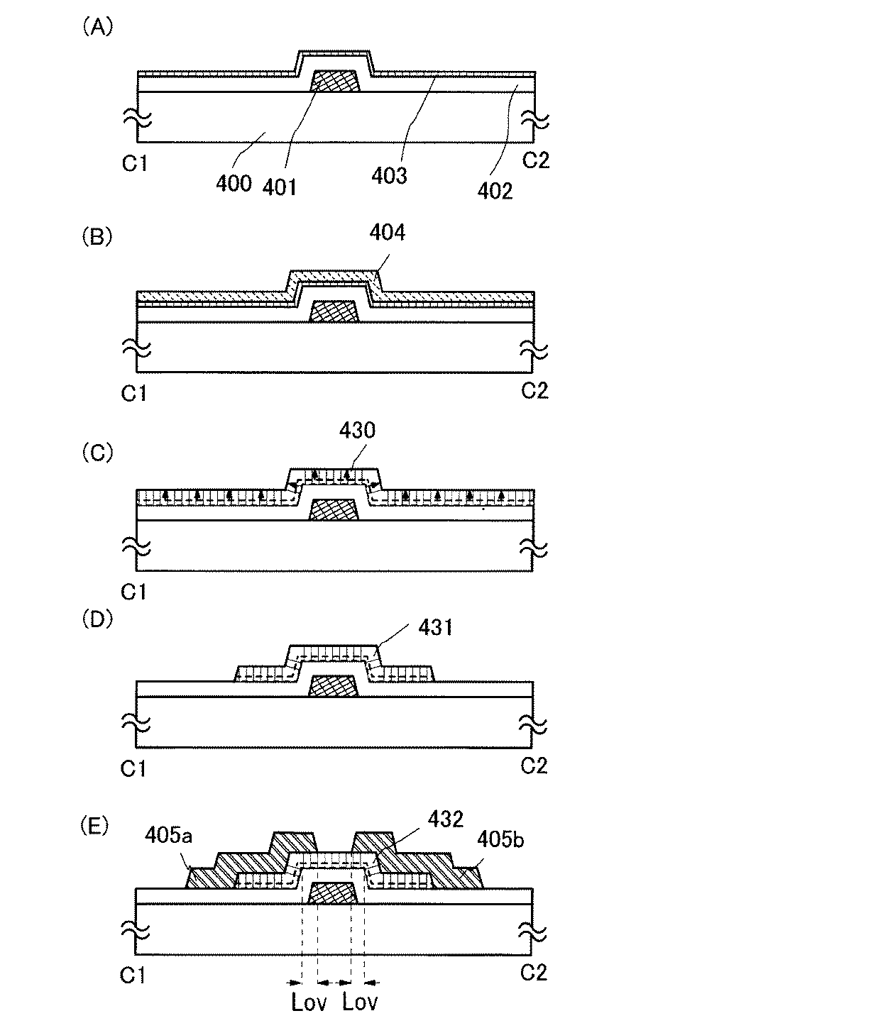
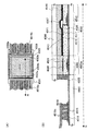
図4に本発明の実施形態を示す。図4(A)はガラス基板1501上に、画素部1502、ゲートドライバ1503、1504を内蔵し、ソース線駆動にアナログスイッチ1505を内蔵した表示装置である。ソース線駆動にアナログスイッチ1505を使用するのは以下の理由による。例えばフルハイビジョン表示装置の場合ソース信号線は1920xRGBの5760本存在する。ソースドライバを同一基板上に形成しない場合は、この端子にそれぞれソースドライバの端子が接続される。そのため、機械的な衝撃などにより、端子の接触不良が発生しやすいという問題があった。端子を減らすことが接触不良低減に有効である。そこでアナログスイッチアレイを同一基板上に形成し、RGBの各端子を時分割で選択的にソースドライバに接続し、端子数を減らすことを目的としている。
図6にソースドライバを内蔵した表示装置の実施形態を示す。図6(A)に示すのはガラス基板1701上に画素部1702、ゲートドライバ1703、1704、ソースドライバ1705を内蔵した例である。ゲートドライバ1703、1704、ソースドライバ1705にはFPC1706、1707より信号が供給される。ゲートドライバ1703、1704を表示装置の左右両側に配置し、画素を駆動することによって、片側の場合の半分の駆動能力で駆動することが可能である。
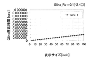
ソース線駆動にアナログスイッチを使用した場合の計算結果を以下に示す。計算は表示装置を100インチの液晶表示装置、フレーム周波数を240Hz(4倍速)の場合を想定している。前述したように4倍速ではソース線の書き込みを0.7μs以下でおこなう必要がある。このときのサンプリング用アナログスイッチに用いるトランジスタ素子サイズはL/W=3μm/1500μm、電界効果移動度は100cm2/Vs、しきい値1.5Vとした。そして、ソース信号線のシート抵抗を0.01Ω/□、ソース線抵抗を2.08KΩ、ソース線容量を18.5pF、線幅6μmとした。そしてソース線電位が期待値の99.9%まで書き込みができることを目標としている。
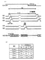
また、ソース線駆動にシフトレジスタ型ソースドライバを使用した場合の計算結果を示す。シフトレジスタは図9に示すようなセットリセット型のシフトレジスタを用いた。また、ソースドライバは図6(B)に示すような配置を仮定し駆動をおこなうものとした。サンプリングは960点同時サンプリングとしている。フルハイビジョンの4分の1の領域を1つのソースドライバで書き込むため、サンプリングすべき点は960xRGB=2880点である。これを960点同時サンプリングするため必要なシフトレジスタの段数は30段となる。そのタイミングチャートを図10(A)に示す。また図10(A)にて設定される期間を図10(B)に示す。ソースドライバのクロック周波数は図10(B)のBの期間の2倍の逆数にあたる。
本実施の形態では、トランジスタの作製例の一例を図1、図2、及び図3を用いて示す。
より金属導電膜を形成した後、フォトリソグラフィ工程によりレジストマスクを形成し、
選択的にエッチングを行って金属電極層を形成する。
実施の形態5は、第1の酸化物部材と第2の酸化物部材に同一成分を含む酸化物半導体材料を用いる場合を示したが、本実施の形態では異なる成分の酸化物半導体材料を用いる場合を示す。
本実施の形態では、c軸配向した結晶層を有する積層酸化物材料を含むトランジスタを作製し、該トランジスタを画素部、さらには駆動回路に用いて表示機能を有する半導体装置(表示装置ともいう)を作製する場合について説明する。また、トランジスタを、駆動回路の一部または全体を、画素部と同一基板上に形成し、システムオンパネルを形成することができる。
半導体装置の一形態に相当する発光表示パネル(発光パネルともいう)の外観及び断面について、図19を用いて説明する。図19(A)は、第1の基板上に形成されたc軸配向した結晶層を有する積層酸化物材料を含むトランジスタ及び発光素子を、第2の基板との間にシール材によって封止した、パネルの平面図であり、図19(B)は、図19(A)のH−Iにおける断面図に相当する。
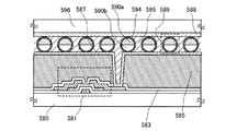
半導体装置の一形態として電子ペーパーの例を示す。
含む)とする。
あるため、電波発信源から表示機能付き半導体装置(単に表示装置、又は表示装置を具備する半導体装置ともいう)を遠ざけた場合であっても、表示された像を保存しておくことが可能となる。
である。
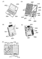
本明細書に開示する半導体装置は、さまざまな電子機器(遊技機も含む)に適用することができる。電子機器としては、例えば、テレビジョン装置(テレビ、またはテレビジョン受信機ともいう)、コンピュータ用などのモニタ、デジタルカメラ、デジタルビデオカメラ、デジタルフォトフレーム、携帯電話機(携帯電話、携帯電話装置ともいう)、携帯型ゲーム機、携帯情報端末、音響再生装置、パチンコ機などの大型ゲーム機などが挙げられる。
401 ゲート電極層
402 ゲート絶縁層
403 第1の酸化物半導体層
404 第2の酸化物半導体層
405a ソース電極層
405b ドレイン電極層
407 酸化物絶縁層
430 酸化物半導体積層
431 島状の酸化物半導体積層
432 酸化物半導体積層
470 トランジスタ
500 下地部材
501 第1の酸化物結晶部材
502 酸化物半導体層
503a 酸化物結晶部材
503b 酸化物結晶部材
504 非晶質を含む層
520 下地部材
531 酸化物結晶部材
532 酸化物部材
533a 酸化物結晶部材
533b 酸化物結晶部材
580 基板
581 トランジスタ
583 絶縁層
585 絶縁層
587 電極層
588 電極層
589 球形粒子
590a 黒色領域
590b 白色領域
594 キャビティ
595 充填材
596 基板
1501 ガラス基板
1502 画素部
1503 ゲートドライバ
1504 ゲートドライバ
1505 アナログスイッチ
1506 FPC
1507 FPC
1508 FPC
1509 FPC
1701 ガラス基板
1702 画素部
1703 ゲートドライバ
1704 ゲートドライバ
1705 ソースドライバ
1706 FPC
1707 FPC
1711 ガラス基板
1712 画素部
1713 ゲートドライバ
1714 ゲートドライバ
1715 ゲートドライバ
1716 ゲートドライバ
1717 ソースドライバ
1718 ソースドライバ
1719 ソースドライバ
1720 ソースドライバ
1721 FPC
1722 FPC
1723 FPC
1724 FPC
2700 電子書籍
2701 筐体
2703 筐体
2705 表示部
2707 表示部
2711 軸部
2721 電源
2723 操作キー
2725 スピーカ
2800 筐体
2801 筐体
2802 表示パネル
2803 スピーカー
2804 マイクロフォン
2805 操作キー
2806 ポインティングデバイス
2807 カメラ用レンズ
2808 外部接続端子
2810 太陽電池セル
2811 外部メモリスロット
3001 本体
3002 筐体
3003 表示部
3004 キーボード
3021 本体
3022 スタイラス
3023 表示部
3024 操作ボタン
3025 外部インターフェイス
3051 本体
3053 接眼部
3054 操作スイッチ
3055 表示部(B)
3056 バッテリー
3057 表示部(A)
4001 基板
4002 画素部
4003 信号線駆動回路
4004 走査線駆動回路
4005 シール材
4006 基板
4008 液晶層
4010 トランジスタ
4011 トランジスタ
4013 液晶素子
4015 接続端子電極
4016 端子電極
4018 FPC
4019 異方性導電層
4020 絶縁層
4021 絶縁層
4030 画素電極層
4031 対向電極層
4032 絶縁層
4033 絶縁層
4035 スペーサー
4040 導電層
4501 基板
4502 画素部
4503a 信号線駆動回路
4503b 信号線駆動回路
4504a 走査線駆動回路
4504b 走査線駆動回路
4505 シール材
4506 基板
4507 充填材
4509 トランジスタ
4510 トランジスタ
4511 発光素子
4512 電界発光層
4513 電極層
4515 接続端子電極
4516 端子電極
4517 電極層
4518a FPC
4518b FPC
4519 異方性導電層
4520 隔壁
4540 導電層
4541 絶縁層
4544 絶縁層
9600 テレビジョン装置
9601 筐体
9603 表示部
9605 スタンド
9607 表示部
9609 操作キー
9610 リモコン操作機
Claims (4)
- 絶縁基板上に複数の画素と複数の信号線、及び複数の走査線を有するアクティブマトリクス型表示装置であり、
前記絶縁基板上に、電界効果移動度が少なくとも50cm2/Vs以上であるトランジスタを有し、
前記トランジスタを1つの構成要素とするゲートドライバ、及びソース線駆動アナログスイッチを有し、
前記トランジスタは、酸化物半導体層を有し、
前記酸化物半導体層は、ゲート絶縁層を介してゲート電極層と重なるチャネル形成領域を少なくとも有し、
前記酸化物半導体層は、第1の金属酸化物層と、第2の金属酸化物層とが積層され、
前記第1の金属酸化物層は、前記第1の金属酸化物層の表面に対して垂直な方向に沿うようにc軸配向した結晶を有し、
前記第2の金属酸化物層は、前記第2の金属酸化物層の表面に対して垂直な方向に沿うようにc軸配向した結晶を有し、
前記第1の金属酸化物層の結晶構造の格子定数と、前記第2の金属酸化物層の結晶構造の格子定数との、ミスマッチは1%以下であることを特徴とする表示装置。 - 絶縁基板上に複数の画素と複数の信号線、及び複数の走査線を有するアクティブマトリクス型表示装置であり、
前記絶縁基板上に、電界効果移動度が100cm2/Vs以上であるトランジスタを有し、
前記トランジスタを1つの構成要素とするゲートドライバ、及びソース線駆動アナログスイッチを有し、
前記トランジスタは、酸化物半導体層を有し、
前記酸化物半導体層は、ゲート絶縁層を介してゲート電極層と重なるチャネル形成領域を少なくとも有し、
前記酸化物半導体層は、第1の金属酸化物層と、第2の金属酸化物層とが積層され、
前記第1の金属酸化物層は、前記第1の金属酸化物層の表面に対して垂直な方向に沿うようにc軸配向した結晶を有し、
前記第2の金属酸化物層は、前記第2の金属酸化物層の表面に対して垂直な方向に沿うようにc軸配向した結晶を有し、
前記第1の金属酸化物層の結晶構造の格子定数と、前記第2の金属酸化物層の結晶構造の格子定数との、ミスマッチは1%以下であることを特徴とする表示装置。 - 請求項1または2において、
前記酸化物半導体層は、Inと、Gaと、Znと、を有することを特徴とする表示装置。 - 請求項1乃至3のいずれか一において、
前記ゲートドライバ、及び前記ソース線駆動アナログスイッチは、同一絶縁基板上に設けられていることを特徴とする表示装置。
Priority Applications (1)
| Application Number | Priority Date | Filing Date | Title |
|---|---|---|---|
| JP2010269522A JP5778919B2 (ja) | 2009-12-04 | 2010-12-02 | 表示装置 |
Applications Claiming Priority (3)
| Application Number | Priority Date | Filing Date | Title |
|---|---|---|---|
| JP2009276918 | 2009-12-04 | ||
| JP2009276918 | 2009-12-04 | ||
| JP2010269522A JP5778919B2 (ja) | 2009-12-04 | 2010-12-02 | 表示装置 |
Related Child Applications (1)
| Application Number | Title | Priority Date | Filing Date |
|---|---|---|---|
| JP2014207209A Division JP5735692B2 (ja) | 2009-12-04 | 2014-10-08 | 表示装置 |
Publications (3)
| Publication Number | Publication Date |
|---|---|
| JP2011139056A JP2011139056A (ja) | 2011-07-14 |
| JP2011139056A5 JP2011139056A5 (ja) | 2014-01-09 |
| JP5778919B2 true JP5778919B2 (ja) | 2015-09-16 |
Family
ID=44114873
Family Applications (11)
| Application Number | Title | Priority Date | Filing Date |
|---|---|---|---|
| JP2010269522A Active JP5778919B2 (ja) | 2009-12-04 | 2010-12-02 | 表示装置 |
| JP2014207209A Active JP5735692B2 (ja) | 2009-12-04 | 2014-10-08 | 表示装置 |
| JP2015084032A Active JP5978342B2 (ja) | 2009-12-04 | 2015-04-16 | 表示装置 |
| JP2016145128A Active JP6211149B2 (ja) | 2009-12-04 | 2016-07-25 | 表示装置 |
| JP2017174803A Active JP6370979B2 (ja) | 2009-12-04 | 2017-09-12 | 表示装置 |
| JP2018131177A Active JP6553258B2 (ja) | 2009-12-04 | 2018-07-11 | 表示装置 |
| JP2019124128A Active JP6840193B2 (ja) | 2009-12-04 | 2019-07-03 | トランジスタ |
| JP2021022365A Active JP7039742B2 (ja) | 2009-12-04 | 2021-02-16 | トランジスタ |
| JP2022036123A Active JP7362811B2 (ja) | 2009-12-04 | 2022-03-09 | 表示装置 |
| JP2023172795A Active JP7635332B2 (ja) | 2009-12-04 | 2023-10-04 | 表示装置 |
| JP2025020575A Pending JP2025087713A (ja) | 2009-12-04 | 2025-02-12 | 表示装置 |
Family Applications After (10)
| Application Number | Title | Priority Date | Filing Date |
|---|---|---|---|
| JP2014207209A Active JP5735692B2 (ja) | 2009-12-04 | 2014-10-08 | 表示装置 |
| JP2015084032A Active JP5978342B2 (ja) | 2009-12-04 | 2015-04-16 | 表示装置 |
| JP2016145128A Active JP6211149B2 (ja) | 2009-12-04 | 2016-07-25 | 表示装置 |
| JP2017174803A Active JP6370979B2 (ja) | 2009-12-04 | 2017-09-12 | 表示装置 |
| JP2018131177A Active JP6553258B2 (ja) | 2009-12-04 | 2018-07-11 | 表示装置 |
| JP2019124128A Active JP6840193B2 (ja) | 2009-12-04 | 2019-07-03 | トランジスタ |
| JP2021022365A Active JP7039742B2 (ja) | 2009-12-04 | 2021-02-16 | トランジスタ |
| JP2022036123A Active JP7362811B2 (ja) | 2009-12-04 | 2022-03-09 | 表示装置 |
| JP2023172795A Active JP7635332B2 (ja) | 2009-12-04 | 2023-10-04 | 表示装置 |
| JP2025020575A Pending JP2025087713A (ja) | 2009-12-04 | 2025-02-12 | 表示装置 |
Country Status (5)
| Country | Link |
|---|---|
| US (9) | US8247813B2 (ja) |
| JP (11) | JP5778919B2 (ja) |
| KR (6) | KR102153034B1 (ja) |
| TW (3) | TWI654688B (ja) |
| WO (1) | WO2011068017A1 (ja) |
Cited By (1)
| Publication number | Priority date | Publication date | Assignee | Title |
|---|---|---|---|---|
| JP2017085185A (ja) * | 2009-12-11 | 2017-05-18 | 株式会社半導体エネルギー研究所 | 半導体装置及び電子機器 |
Families Citing this family (66)
| Publication number | Priority date | Publication date | Assignee | Title |
|---|---|---|---|---|
| EP2486593B1 (en) | 2009-10-09 | 2017-02-01 | Semiconductor Energy Laboratory Co., Ltd. | Semiconductor device and manufacturing method thereof |
| KR101876473B1 (ko) | 2009-11-06 | 2018-07-10 | 가부시키가이샤 한도오따이 에네루기 켄큐쇼 | 반도체 장치 및 반도체 장치의 제작 방법 |
| WO2011065210A1 (en) * | 2009-11-28 | 2011-06-03 | Semiconductor Energy Laboratory Co., Ltd. | Stacked oxide material, semiconductor device, and method for manufacturing the semiconductor device |
| KR101825345B1 (ko) | 2009-11-28 | 2018-02-05 | 가부시키가이샤 한도오따이 에네루기 켄큐쇼 | 적층 산화물 재료, 반도체 장치 및 반도체 장치의 제작 방법 |
| KR102153034B1 (ko) | 2009-12-04 | 2020-09-07 | 가부시키가이샤 한도오따이 에네루기 켄큐쇼 | 반도체 장치 |
| CN105609509A (zh) | 2009-12-04 | 2016-05-25 | 株式会社半导体能源研究所 | 显示装置 |
| WO2011074407A1 (en) * | 2009-12-18 | 2011-06-23 | Semiconductor Energy Laboratory Co., Ltd. | Semiconductor device and method for manufacturing the same |
| CN109390215B (zh) | 2009-12-28 | 2023-08-15 | 株式会社半导体能源研究所 | 制造半导体装置的方法 |
| WO2011108346A1 (en) | 2010-03-05 | 2011-09-09 | Semiconductor Energy Laboratory Co., Ltd. | Manufacturing method of oxide semiconductor film and manufacturing method of transistor |
| US8629438B2 (en) | 2010-05-21 | 2014-01-14 | Semiconductor Energy Laboratory Co., Ltd. | Semiconductor device and manufacturing method thereof |
| JP5458443B2 (ja) * | 2010-09-14 | 2014-04-02 | 株式会社ジャパンディスプレイ | タッチ検出機能付き表示装置、および電子機器 |
| KR101900525B1 (ko) * | 2011-03-18 | 2018-09-19 | 가부시키가이샤 한도오따이 에네루기 켄큐쇼 | 산화물 반도체막, 반도체 장치, 및 반도체 장치의 제작 방법 |
| US8932913B2 (en) | 2011-04-22 | 2015-01-13 | Semiconductor Energy Laboratory Co., Ltd. | Manufacturing method of semiconductor device |
| US8878288B2 (en) | 2011-04-22 | 2014-11-04 | Semiconductor Energy Laboratory Co., Ltd. | Semiconductor device |
| US8916868B2 (en) | 2011-04-22 | 2014-12-23 | Semiconductor Energy Laboratory Co., Ltd. | Semiconductor device and method for manufacturing semiconductor device |
| US8809854B2 (en) | 2011-04-22 | 2014-08-19 | Semiconductor Energy Laboratory Co., Ltd. | Semiconductor device |
| US8946066B2 (en) | 2011-05-11 | 2015-02-03 | Semiconductor Energy Laboratory Co., Ltd. | Method of manufacturing semiconductor device |
| US8847233B2 (en) | 2011-05-12 | 2014-09-30 | Semiconductor Energy Laboratory Co., Ltd. | Semiconductor device having a trenched insulating layer coated with an oxide semiconductor film |
| US9954110B2 (en) | 2011-05-13 | 2018-04-24 | Semiconductor Energy Laboratory Co., Ltd. | EL display device and electronic device |
| JP6110075B2 (ja) | 2011-05-13 | 2017-04-05 | 株式会社半導体エネルギー研究所 | 表示装置 |
| CN107419225B (zh) | 2011-06-08 | 2020-08-04 | 株式会社半导体能源研究所 | 溅射靶材、溅射靶材的制造方法及薄膜形成方法 |
| US9130044B2 (en) | 2011-07-01 | 2015-09-08 | Semiconductor Energy Laboratory Co., Ltd. | Semiconductor device and manufacturing method thereof |
| US8952377B2 (en) | 2011-07-08 | 2015-02-10 | Semiconductor Energy Laboratory Co., Ltd. | Semiconductor device and manufacturing method thereof |
| KR101962261B1 (ko) * | 2011-07-15 | 2019-03-26 | 가부시키가이샤 한도오따이 에네루기 켄큐쇼 | 반도체 장치 및 반도체 장치의 구동 방법 |
| KR101953724B1 (ko) | 2011-08-26 | 2019-03-04 | 가부시키가이샤 한도오따이 에네루기 켄큐쇼 | 발광 모듈, 발광 장치, 발광 모듈의 제작 방법, 발광 장치의 제작 방법 |
| US9431545B2 (en) | 2011-09-23 | 2016-08-30 | Semiconductor Energy Laboratory Co., Ltd. | Semiconductor device and method for manufacturing the same |
| KR102504604B1 (ko) | 2011-09-29 | 2023-02-27 | 가부시키가이샤 한도오따이 에네루기 켄큐쇼 | 반도체 장치 |
| US8637864B2 (en) | 2011-10-13 | 2014-01-28 | Semiconductor Energy Laboratory Co., Ltd. | Semiconductor device and method of manufacturing the same |
| JP5912394B2 (ja) | 2011-10-13 | 2016-04-27 | 株式会社半導体エネルギー研究所 | 半導体装置 |
| US10002968B2 (en) * | 2011-12-14 | 2018-06-19 | Semiconductor Energy Laboratory Co., Ltd. | Semiconductor device and display device including the same |
| JP6053490B2 (ja) | 2011-12-23 | 2016-12-27 | 株式会社半導体エネルギー研究所 | 半導体装置の作製方法 |
| KR102479944B1 (ko) | 2012-04-13 | 2022-12-20 | 가부시키가이샤 한도오따이 에네루기 켄큐쇼 | 반도체 장치 |
| JP6076612B2 (ja) * | 2012-04-17 | 2017-02-08 | 株式会社半導体エネルギー研究所 | 半導体装置 |
| KR102119914B1 (ko) * | 2012-05-31 | 2020-06-05 | 가부시키가이샤 한도오따이 에네루기 켄큐쇼 | 반도체 장치 및 그 제작 방법 |
| JP6043244B2 (ja) * | 2012-06-06 | 2016-12-14 | 株式会社神戸製鋼所 | 薄膜トランジスタ |
| US9885108B2 (en) | 2012-08-07 | 2018-02-06 | Semiconductor Energy Laboratory Co., Ltd. | Method for forming sputtering target |
| CN102856392B (zh) * | 2012-10-09 | 2015-12-02 | 深圳市华星光电技术有限公司 | 薄膜晶体管主动装置及其制作方法 |
| US20140151095A1 (en) * | 2012-12-05 | 2014-06-05 | Samsung Electro-Mechanics Co., Ltd. | Printed circuit board and method for manufacturing the same |
| JPWO2014125820A1 (ja) * | 2013-02-13 | 2017-02-02 | 出光興産株式会社 | 薄膜トランジスタ |
| JP6141777B2 (ja) | 2013-02-28 | 2017-06-07 | 株式会社半導体エネルギー研究所 | 半導体装置の作製方法 |
| US10304859B2 (en) | 2013-04-12 | 2019-05-28 | Semiconductor Energy Laboratory Co., Ltd. | Semiconductor device having an oxide film on an oxide semiconductor film |
| KR102089326B1 (ko) * | 2013-10-01 | 2020-03-17 | 엘지디스플레이 주식회사 | 표시장치 |
| US9627413B2 (en) * | 2013-12-12 | 2017-04-18 | Semiconductor Energy Laboratory Co., Ltd. | Semiconductor device and display device |
| JP2015115469A (ja) * | 2013-12-12 | 2015-06-22 | ソニー株式会社 | 薄膜トランジスタ、表示装置、電子機器、および薄膜トランジスタの製造方法 |
| KR102127240B1 (ko) * | 2013-12-13 | 2020-06-26 | 엘지디스플레이 주식회사 | 표시장치 및 그 신호라인, 그 제조방법 |
| TWI545777B (zh) * | 2014-01-15 | 2016-08-11 | Kobe Steel Ltd | Thin film transistor |
| FR3037438B1 (fr) * | 2015-06-09 | 2017-06-16 | Soitec Silicon On Insulator | Procede de fabrication d'un element semi-conducteur comprenant une couche de piegeage de charges |
| US10302019B2 (en) * | 2016-03-03 | 2019-05-28 | General Electric Company | High pressure compressor augmented bleed with autonomously actuated valve |
| KR102640383B1 (ko) | 2016-03-22 | 2024-02-27 | 가부시키가이샤 한도오따이 에네루기 켄큐쇼 | 반도체 장치, 및 상기 반도체 장치를 포함하는 표시 장치 |
| FR3058561B1 (fr) | 2016-11-04 | 2018-11-02 | Soitec | Procede de fabrication d'un element semi-conducteur comprenant un substrat hautement resistif |
| US10866475B2 (en) | 2017-03-17 | 2020-12-15 | Sharp Kabushiki Kaisha | Active matrix substrate and display device |
| WO2018181296A1 (ja) * | 2017-03-29 | 2018-10-04 | シャープ株式会社 | チャネルエッチ型薄膜トランジスタの製造方法 |
| CN107544185B (zh) * | 2017-09-25 | 2020-08-18 | 京东方科技集团股份有限公司 | 阵列基板、显示面板及显示装置 |
| CN107862998B (zh) * | 2017-11-09 | 2020-05-19 | 深圳市华星光电半导体显示技术有限公司 | 一种柔性goa显示面板及其制作方法 |
| CN107919365B (zh) * | 2017-11-21 | 2019-10-11 | 深圳市华星光电半导体显示技术有限公司 | 背沟道蚀刻型tft基板及其制作方法 |
| US11257959B2 (en) | 2017-12-06 | 2022-02-22 | Semiconductor Energy Laboratory Co., Ltd. | Semiconductor device and method for manufacturing the semiconductor device |
| US20190280052A1 (en) * | 2018-03-12 | 2019-09-12 | Wuhan China Star Optoelectronics Semiconductor Display Technology Co., Ltd. | Method for manufacturing a touch-control panel and oled touch-control apparauts |
| JPWO2019224655A1 (ja) * | 2018-05-25 | 2021-07-26 | 株式会社半導体エネルギー研究所 | 表示装置および電子機器 |
| TWI693785B (zh) * | 2019-01-24 | 2020-05-11 | 研能科技股份有限公司 | 微機電泵模組 |
| TWI699086B (zh) * | 2019-01-24 | 2020-07-11 | 研能科技股份有限公司 | 微機電泵模組 |
| TWI697192B (zh) * | 2019-01-24 | 2020-06-21 | 研能科技股份有限公司 | 微機電泵模組 |
| KR20220006547A (ko) | 2019-05-10 | 2022-01-17 | 가부시키가이샤 한도오따이 에네루기 켄큐쇼 | 표시 장치 |
| KR102840468B1 (ko) | 2019-07-16 | 2025-07-29 | 삼성전자주식회사 | 반도체 장치 |
| KR20240095556A (ko) * | 2022-11-30 | 2024-06-26 | 삼성디스플레이 주식회사 | 표시 장치 |
| KR20240134617A (ko) * | 2023-03-02 | 2024-09-10 | 삼성전자주식회사 | 디스플레이 장치 |
| CN118884712A (zh) * | 2024-08-14 | 2024-11-01 | 业桓科技(成都)有限公司 | 光学系统及头戴式显示设备 |
Family Cites Families (159)
| Publication number | Priority date | Publication date | Assignee | Title |
|---|---|---|---|---|
| JPS60198861A (ja) | 1984-03-23 | 1985-10-08 | Fujitsu Ltd | 薄膜トランジスタ |
| JPH0244256B2 (ja) | 1987-01-28 | 1990-10-03 | Kagaku Gijutsucho Mukizaishitsu Kenkyushocho | Ingazn2o5deshimesarerurotsuhoshokeinosojokozoojusurukagobutsuoyobisonoseizoho |
| JPH0244258B2 (ja) | 1987-02-24 | 1990-10-03 | Kagaku Gijutsucho Mukizaishitsu Kenkyushocho | Ingazn3o6deshimesarerurotsuhoshokeinosojokozoojusurukagobutsuoyobisonoseizoho |
| JPS63210023A (ja) | 1987-02-24 | 1988-08-31 | Natl Inst For Res In Inorg Mater | InGaZn↓4O↓7で示される六方晶系の層状構造を有する化合物およびその製造法 |
| JPH0244260B2 (ja) | 1987-02-24 | 1990-10-03 | Kagaku Gijutsucho Mukizaishitsu Kenkyushocho | Ingazn5o8deshimesarerurotsuhoshokeinosojokozoojusurukagobutsuoyobisonoseizoho |
| JPH0244262B2 (ja) | 1987-02-27 | 1990-10-03 | Kagaku Gijutsucho Mukizaishitsu Kenkyushocho | Ingazn6o9deshimesarerurotsuhoshokeinosojokozoojusurukagobutsuoyobisonoseizoho |
| JPH0244263B2 (ja) | 1987-04-22 | 1990-10-03 | Kagaku Gijutsucho Mukizaishitsu Kenkyushocho | Ingazn7o10deshimesarerurotsuhoshokeinosojokozoojusurukagobutsuoyobisonoseizoho |
| JPH05251705A (ja) | 1992-03-04 | 1993-09-28 | Fuji Xerox Co Ltd | 薄膜トランジスタ |
| JP3479375B2 (ja) | 1995-03-27 | 2003-12-15 | 科学技術振興事業団 | 亜酸化銅等の金属酸化物半導体による薄膜トランジスタとpn接合を形成した金属酸化物半導体装置およびそれらの製造方法 |
| KR100394896B1 (ko) | 1995-08-03 | 2003-11-28 | 코닌클리케 필립스 일렉트로닉스 엔.브이. | 투명스위칭소자를포함하는반도체장치 |
| JP3625598B2 (ja) | 1995-12-30 | 2005-03-02 | 三星電子株式会社 | 液晶表示装置の製造方法 |
| JP3881407B2 (ja) * | 1996-07-31 | 2007-02-14 | Hoya株式会社 | 導電性酸化物薄膜、この薄膜を有する物品及びその製造方法 |
| US5859630A (en) | 1996-12-09 | 1999-01-12 | Thomson Multimedia S.A. | Bi-directional shift register |
| JP3945887B2 (ja) * | 1998-01-30 | 2007-07-18 | Hoya株式会社 | 導電性酸化物薄膜を有する物品及びその製造方法 |
| JP2000026119A (ja) | 1998-07-09 | 2000-01-25 | Hoya Corp | 透明導電性酸化物薄膜を有する物品及びその製造方法 |
| JP4170454B2 (ja) | 1998-07-24 | 2008-10-22 | Hoya株式会社 | 透明導電性酸化物薄膜を有する物品及びその製造方法 |
| JP2000150861A (ja) | 1998-11-16 | 2000-05-30 | Tdk Corp | 酸化物薄膜 |
| JP3276930B2 (ja) | 1998-11-17 | 2002-04-22 | 科学技術振興事業団 | トランジスタ及び半導体装置 |
| TW460731B (en) | 1999-09-03 | 2001-10-21 | Ind Tech Res Inst | Electrode structure and production method of wide viewing angle LCD |
| WO2002016679A1 (en) * | 2000-08-18 | 2002-02-28 | Tohoku Techno Arch Co., Ltd. | Polycrystalline semiconductor material and method of manufacture thereof |
| JP4089858B2 (ja) | 2000-09-01 | 2008-05-28 | 国立大学法人東北大学 | 半導体デバイス |
| KR20020038482A (ko) | 2000-11-15 | 2002-05-23 | 모리시타 요이찌 | 박막 트랜지스터 어레이, 그 제조방법 및 그것을 이용한표시패널 |
| JP3997731B2 (ja) | 2001-03-19 | 2007-10-24 | 富士ゼロックス株式会社 | 基材上に結晶性半導体薄膜を形成する方法 |
| JP2002289859A (ja) | 2001-03-23 | 2002-10-04 | Minolta Co Ltd | 薄膜トランジスタ |
| JP4090716B2 (ja) | 2001-09-10 | 2008-05-28 | 雅司 川崎 | 薄膜トランジスタおよびマトリクス表示装置 |
| JP3925839B2 (ja) | 2001-09-10 | 2007-06-06 | シャープ株式会社 | 半導体記憶装置およびその試験方法 |
| EP1443130B1 (en) | 2001-11-05 | 2011-09-28 | Japan Science and Technology Agency | Natural superlattice homologous single crystal thin film, method for preparation thereof, and device using said single crystal thin film |
| JP4164562B2 (ja) | 2002-09-11 | 2008-10-15 | 独立行政法人科学技術振興機構 | ホモロガス薄膜を活性層として用いる透明薄膜電界効果型トランジスタ |
| JP4083486B2 (ja) | 2002-02-21 | 2008-04-30 | 独立行政法人科学技術振興機構 | LnCuO(S,Se,Te)単結晶薄膜の製造方法 |
| CN1445821A (zh) | 2002-03-15 | 2003-10-01 | 三洋电机株式会社 | ZnO膜和ZnO半导体层的形成方法、半导体元件及其制造方法 |
| JP3933591B2 (ja) | 2002-03-26 | 2007-06-20 | 淳二 城戸 | 有機エレクトロルミネッセント素子 |
| US7339187B2 (en) | 2002-05-21 | 2008-03-04 | State Of Oregon Acting By And Through The Oregon State Board Of Higher Education On Behalf Of Oregon State University | Transistor structures |
| JP2004022625A (ja) | 2002-06-13 | 2004-01-22 | Murata Mfg Co Ltd | 半導体デバイス及び該半導体デバイスの製造方法 |
| TWI306311B (en) | 2002-06-21 | 2009-02-11 | Sanyo Electric Co | Thin film transistor and method for producing thin film transistor |
| US7105868B2 (en) | 2002-06-24 | 2006-09-12 | Cermet, Inc. | High-electron mobility transistor with zinc oxide |
| US7067843B2 (en) | 2002-10-11 | 2006-06-27 | E. I. Du Pont De Nemours And Company | Transparent oxide semiconductor thin film transistors |
| GB2397710A (en) | 2003-01-25 | 2004-07-28 | Sharp Kk | A shift register for an LCD driver, comprising reset-dominant RS flip-flops |
| JP4166105B2 (ja) | 2003-03-06 | 2008-10-15 | シャープ株式会社 | 半導体装置およびその製造方法 |
| JP2004273732A (ja) | 2003-03-07 | 2004-09-30 | Sharp Corp | アクティブマトリクス基板およびその製造方法 |
| JP4108633B2 (ja) | 2003-06-20 | 2008-06-25 | シャープ株式会社 | 薄膜トランジスタおよびその製造方法ならびに電子デバイス |
| US7262463B2 (en) | 2003-07-25 | 2007-08-28 | Hewlett-Packard Development Company, L.P. | Transistor including a deposited channel region having a doped portion |
| JP2005150203A (ja) | 2003-11-12 | 2005-06-09 | Matsushita Electric Ind Co Ltd | 電界効果トランジスタ及び相補型電界効果トランジスタ並びにこれらの製造方法 |
| US20070194379A1 (en) | 2004-03-12 | 2007-08-23 | Japan Science And Technology Agency | Amorphous Oxide And Thin Film Transistor |
| US7297977B2 (en) | 2004-03-12 | 2007-11-20 | Hewlett-Packard Development Company, L.P. | Semiconductor device |
| US7282782B2 (en) | 2004-03-12 | 2007-10-16 | Hewlett-Packard Development Company, L.P. | Combined binary oxide semiconductor device |
| US7145174B2 (en) | 2004-03-12 | 2006-12-05 | Hewlett-Packard Development Company, Lp. | Semiconductor device |
| KR101058176B1 (ko) | 2004-03-25 | 2011-08-22 | 가부시키가이샤 한도오따이 에네루기 켄큐쇼 | 박막 트랜지스터의 제조 방법 |
| JP4713192B2 (ja) * | 2004-03-25 | 2011-06-29 | 株式会社半導体エネルギー研究所 | 薄膜トランジスタの作製方法 |
| JP4583797B2 (ja) * | 2004-04-14 | 2010-11-17 | 株式会社半導体エネルギー研究所 | 半導体装置の作製方法 |
| US7211825B2 (en) | 2004-06-14 | 2007-05-01 | Yi-Chi Shih | Indium oxide-based thin film transistors and circuits |
| US7622338B2 (en) * | 2004-08-31 | 2009-11-24 | Semiconductor Energy Laboratory Co., Ltd. | Method for manufacturing semiconductor device |
| JP2006100760A (ja) | 2004-09-02 | 2006-04-13 | Casio Comput Co Ltd | 薄膜トランジスタおよびその製造方法 |
| US7285501B2 (en) | 2004-09-17 | 2007-10-23 | Hewlett-Packard Development Company, L.P. | Method of forming a solution processed device |
| US7470604B2 (en) | 2004-10-08 | 2008-12-30 | Semiconductor Energy Laboratory Co., Ltd. | Method for manufacturing display device |
| JP5110785B2 (ja) * | 2004-10-08 | 2012-12-26 | 株式会社半導体エネルギー研究所 | 表示装置の作製方法 |
| US7298084B2 (en) | 2004-11-02 | 2007-11-20 | 3M Innovative Properties Company | Methods and displays utilizing integrated zinc oxide row and column drivers in conjunction with organic light emitting diodes |
| US7829444B2 (en) | 2004-11-10 | 2010-11-09 | Canon Kabushiki Kaisha | Field effect transistor manufacturing method |
| EP2453480A2 (en) | 2004-11-10 | 2012-05-16 | Canon Kabushiki Kaisha | Amorphous oxide and field effect transistor |
| US7791072B2 (en) | 2004-11-10 | 2010-09-07 | Canon Kabushiki Kaisha | Display |
| EP1815530B1 (en) | 2004-11-10 | 2021-02-17 | Canon Kabushiki Kaisha | Field effect transistor employing an amorphous oxide |
| US7863611B2 (en) | 2004-11-10 | 2011-01-04 | Canon Kabushiki Kaisha | Integrated circuits utilizing amorphous oxides |
| US7453065B2 (en) | 2004-11-10 | 2008-11-18 | Canon Kabushiki Kaisha | Sensor and image pickup device |
| AU2005302963B2 (en) | 2004-11-10 | 2009-07-02 | Cannon Kabushiki Kaisha | Light-emitting device |
| US7579224B2 (en) | 2005-01-21 | 2009-08-25 | Semiconductor Energy Laboratory Co., Ltd. | Method for manufacturing a thin film semiconductor device |
| TWI481024B (zh) | 2005-01-28 | 2015-04-11 | 半導體能源研究所股份有限公司 | 半導體裝置,電子裝置,和半導體裝置的製造方法 |
| TWI412138B (zh) | 2005-01-28 | 2013-10-11 | 半導體能源研究所股份有限公司 | 半導體裝置,電子裝置,和半導體裝置的製造方法 |
| US7858451B2 (en) | 2005-02-03 | 2010-12-28 | Semiconductor Energy Laboratory Co., Ltd. | Electronic device, semiconductor device and manufacturing method thereof |
| US7948171B2 (en) | 2005-02-18 | 2011-05-24 | Semiconductor Energy Laboratory Co., Ltd. | Light emitting device |
| US20060197092A1 (en) | 2005-03-03 | 2006-09-07 | Randy Hoffman | System and method for forming conductive material on a substrate |
| US8681077B2 (en) | 2005-03-18 | 2014-03-25 | Semiconductor Energy Laboratory Co., Ltd. | Semiconductor device, and display device, driving method and electronic apparatus thereof |
| US7544967B2 (en) | 2005-03-28 | 2009-06-09 | Massachusetts Institute Of Technology | Low voltage flexible organic/transparent transistor for selective gas sensing, photodetecting and CMOS device applications |
| US7645478B2 (en) | 2005-03-31 | 2010-01-12 | 3M Innovative Properties Company | Methods of making displays |
| US8300031B2 (en) | 2005-04-20 | 2012-10-30 | Semiconductor Energy Laboratory Co., Ltd. | Semiconductor device comprising transistor having gate and drain connected through a current-voltage conversion element |
| JP2006344849A (ja) | 2005-06-10 | 2006-12-21 | Casio Comput Co Ltd | 薄膜トランジスタ |
| US7691666B2 (en) | 2005-06-16 | 2010-04-06 | Eastman Kodak Company | Methods of making thin film transistors comprising zinc-oxide-based semiconductor materials and transistors made thereby |
| US7402506B2 (en) | 2005-06-16 | 2008-07-22 | Eastman Kodak Company | Methods of making thin film transistors comprising zinc-oxide-based semiconductor materials and transistors made thereby |
| US7507618B2 (en) | 2005-06-27 | 2009-03-24 | 3M Innovative Properties Company | Method for making electronic devices using metal oxide nanoparticles |
| KR100711890B1 (ko) | 2005-07-28 | 2007-04-25 | 삼성에스디아이 주식회사 | 유기 발광표시장치 및 그의 제조방법 |
| JP2007059128A (ja) | 2005-08-23 | 2007-03-08 | Canon Inc | 有機el表示装置およびその製造方法 |
| JP5116225B2 (ja) | 2005-09-06 | 2013-01-09 | キヤノン株式会社 | 酸化物半導体デバイスの製造方法 |
| JP4850457B2 (ja) | 2005-09-06 | 2012-01-11 | キヤノン株式会社 | 薄膜トランジスタ及び薄膜ダイオード |
| JP4280736B2 (ja) | 2005-09-06 | 2009-06-17 | キヤノン株式会社 | 半導体素子 |
| JP2007073705A (ja) | 2005-09-06 | 2007-03-22 | Canon Inc | 酸化物半導体チャネル薄膜トランジスタおよびその製造方法 |
| EP3614442A3 (en) * | 2005-09-29 | 2020-03-25 | Semiconductor Energy Laboratory Co., Ltd. | Semiconductor device having oxide semiconductor layer and manufactoring method thereof |
| JP5064747B2 (ja) | 2005-09-29 | 2012-10-31 | 株式会社半導体エネルギー研究所 | 半導体装置、電気泳動表示装置、表示モジュール、電子機器、及び半導体装置の作製方法 |
| JP5078246B2 (ja) | 2005-09-29 | 2012-11-21 | 株式会社半導体エネルギー研究所 | 半導体装置、及び半導体装置の作製方法 |
| JP5037808B2 (ja) | 2005-10-20 | 2012-10-03 | キヤノン株式会社 | アモルファス酸化物を用いた電界効果型トランジスタ、及び該トランジスタを用いた表示装置 |
| JP5089139B2 (ja) * | 2005-11-15 | 2012-12-05 | 株式会社半導体エネルギー研究所 | 半導体装置の作製方法 |
| CN101667544B (zh) | 2005-11-15 | 2012-09-05 | 株式会社半导体能源研究所 | 半导体器件及其制造方法 |
| TWI292281B (en) | 2005-12-29 | 2008-01-01 | Ind Tech Res Inst | Pixel structure of active organic light emitting diode and method of fabricating the same |
| KR101437086B1 (ko) | 2006-01-07 | 2014-09-03 | 가부시키가이샤 한도오따이 에네루기 켄큐쇼 | 반도체장치와, 이 반도체장치를 구비한 표시장치 및 전자기기 |
| US7867636B2 (en) | 2006-01-11 | 2011-01-11 | Murata Manufacturing Co., Ltd. | Transparent conductive film and method for manufacturing the same |
| JP4977478B2 (ja) | 2006-01-21 | 2012-07-18 | 三星電子株式会社 | ZnOフィルム及びこれを用いたTFTの製造方法 |
| US7576394B2 (en) | 2006-02-02 | 2009-08-18 | Kochi Industrial Promotion Center | Thin film transistor including low resistance conductive thin films and manufacturing method thereof |
| JP5015473B2 (ja) | 2006-02-15 | 2012-08-29 | 財団法人高知県産業振興センター | 薄膜トランジスタアレイ及びその製法 |
| US7977169B2 (en) * | 2006-02-15 | 2011-07-12 | Kochi Industrial Promotion Center | Semiconductor device including active layer made of zinc oxide with controlled orientations and manufacturing method thereof |
| KR20070101595A (ko) | 2006-04-11 | 2007-10-17 | 삼성전자주식회사 | ZnO TFT |
| JP5271504B2 (ja) * | 2006-04-28 | 2013-08-21 | 株式会社半導体エネルギー研究所 | 半導体装置の作製方法 |
| US20070252928A1 (en) | 2006-04-28 | 2007-11-01 | Toppan Printing Co., Ltd. | Structure, transmission type liquid crystal display, reflection type display and manufacturing method thereof |
| US20070252233A1 (en) | 2006-04-28 | 2007-11-01 | Semiconductor Energy Laboratory Co., Ltd. | Semiconductor device and method for manufacturing the semiconductor device |
| WO2007142167A1 (en) | 2006-06-02 | 2007-12-13 | Kochi Industrial Promotion Center | Semiconductor device including an oxide semiconductor thin film layer of zinc oxide and manufacturing method thereof |
| US20070287221A1 (en) | 2006-06-12 | 2007-12-13 | Xerox Corporation | Fabrication process for crystalline zinc oxide semiconductor layer |
| JP5028033B2 (ja) | 2006-06-13 | 2012-09-19 | キヤノン株式会社 | 酸化物半導体膜のドライエッチング方法 |
| US7906415B2 (en) | 2006-07-28 | 2011-03-15 | Xerox Corporation | Device having zinc oxide semiconductor and indium/zinc electrode |
| JP4999400B2 (ja) | 2006-08-09 | 2012-08-15 | キヤノン株式会社 | 酸化物半導体膜のドライエッチング方法 |
| JP4609797B2 (ja) | 2006-08-09 | 2011-01-12 | Nec液晶テクノロジー株式会社 | 薄膜デバイス及びその製造方法 |
| JP4332545B2 (ja) | 2006-09-15 | 2009-09-16 | キヤノン株式会社 | 電界効果型トランジスタ及びその製造方法 |
| JP5164357B2 (ja) | 2006-09-27 | 2013-03-21 | キヤノン株式会社 | 半導体装置及び半導体装置の製造方法 |
| JP4274219B2 (ja) | 2006-09-27 | 2009-06-03 | セイコーエプソン株式会社 | 電子デバイス、有機エレクトロルミネッセンス装置、有機薄膜半導体装置 |
| JP4932415B2 (ja) | 2006-09-29 | 2012-05-16 | 株式会社半導体エネルギー研究所 | 半導体装置 |
| TW202429692A (zh) | 2006-09-29 | 2024-07-16 | 日商半導體能源研究所股份有限公司 | 半導體裝置 |
| US7622371B2 (en) | 2006-10-10 | 2009-11-24 | Hewlett-Packard Development Company, L.P. | Fused nanocrystal thin film semiconductor and method |
| US7511343B2 (en) | 2006-10-12 | 2009-03-31 | Xerox Corporation | Thin film transistor |
| JP2008116652A (ja) * | 2006-11-02 | 2008-05-22 | Seiko Epson Corp | 配線基板およびその製造方法、並びに電子機器 |
| US7772021B2 (en) | 2006-11-29 | 2010-08-10 | Samsung Electronics Co., Ltd. | Flat panel displays comprising a thin-film transistor having a semiconductive oxide in its channel and methods of fabricating the same for use in flat panel displays |
| JP2008140684A (ja) | 2006-12-04 | 2008-06-19 | Toppan Printing Co Ltd | カラーelディスプレイおよびその製造方法 |
| US8143115B2 (en) | 2006-12-05 | 2012-03-27 | Canon Kabushiki Kaisha | Method for manufacturing thin film transistor using oxide semiconductor and display apparatus |
| KR101303578B1 (ko) | 2007-01-05 | 2013-09-09 | 삼성전자주식회사 | 박막 식각 방법 |
| US8207063B2 (en) | 2007-01-26 | 2012-06-26 | Eastman Kodak Company | Process for atomic layer deposition |
| TWI478347B (zh) | 2007-02-09 | 2015-03-21 | Idemitsu Kosan Co | A thin film transistor, a thin film transistor substrate, and an image display device, and an image display device, and a semiconductor device |
| KR100851215B1 (ko) | 2007-03-14 | 2008-08-07 | 삼성에스디아이 주식회사 | 박막 트랜지스터 및 이를 이용한 유기 전계 발광표시장치 |
| JP5466939B2 (ja) | 2007-03-23 | 2014-04-09 | 出光興産株式会社 | 半導体デバイス、多結晶半導体薄膜、多結晶半導体薄膜の製造方法、電界効果型トランジスタ、及び、電界効果型トランジスタの製造方法 |
| JP5197058B2 (ja) | 2007-04-09 | 2013-05-15 | キヤノン株式会社 | 発光装置とその作製方法 |
| WO2008126879A1 (en) | 2007-04-09 | 2008-10-23 | Canon Kabushiki Kaisha | Light-emitting apparatus and production method thereof |
| US7795613B2 (en) | 2007-04-17 | 2010-09-14 | Toppan Printing Co., Ltd. | Structure with transistor |
| KR101325053B1 (ko) | 2007-04-18 | 2013-11-05 | 삼성디스플레이 주식회사 | 박막 트랜지스터 기판 및 이의 제조 방법 |
| KR20080094300A (ko) | 2007-04-19 | 2008-10-23 | 삼성전자주식회사 | 박막 트랜지스터 및 그 제조 방법과 박막 트랜지스터를포함하는 평판 디스플레이 |
| KR101334181B1 (ko) | 2007-04-20 | 2013-11-28 | 삼성전자주식회사 | 선택적으로 결정화된 채널층을 갖는 박막 트랜지스터 및 그제조 방법 |
| US8274078B2 (en) | 2007-04-25 | 2012-09-25 | Canon Kabushiki Kaisha | Metal oxynitride semiconductor containing zinc |
| JP5043499B2 (ja) * | 2007-05-02 | 2012-10-10 | 財団法人高知県産業振興センター | 電子素子及び電子素子の製造方法 |
| WO2008136505A1 (ja) * | 2007-05-08 | 2008-11-13 | Idemitsu Kosan Co., Ltd. | 半導体デバイス及び薄膜トランジスタ、並びに、それらの製造方法 |
| JP5164427B2 (ja) * | 2007-05-11 | 2013-03-21 | 株式会社ジャパンディスプレイウェスト | 半導体装置およびその駆動方法、表示装置およびその駆動方法 |
| JP5215589B2 (ja) | 2007-05-11 | 2013-06-19 | キヤノン株式会社 | 絶縁ゲート型トランジスタ及び表示装置 |
| JP4462289B2 (ja) | 2007-05-18 | 2010-05-12 | ソニー株式会社 | 半導体層の成長方法および半導体発光素子の製造方法 |
| KR101345376B1 (ko) | 2007-05-29 | 2013-12-24 | 삼성전자주식회사 | ZnO 계 박막 트랜지스터 및 그 제조방법 |
| US8354674B2 (en) * | 2007-06-29 | 2013-01-15 | Semiconductor Energy Laboratory Co., Ltd. | Semiconductor device wherein a property of a first semiconductor layer is different from a property of a second semiconductor layer |
| JP5354999B2 (ja) | 2007-09-26 | 2013-11-27 | キヤノン株式会社 | 電界効果型トランジスタの製造方法 |
| JP2009135448A (ja) * | 2007-11-01 | 2009-06-18 | Semiconductor Energy Lab Co Ltd | 半導体基板の作製方法及び半導体装置の作製方法 |
| US7768008B2 (en) | 2007-11-13 | 2010-08-03 | Toppan Printing Co., Ltd. | Thin film transistor, method for manufacturing the same and display using the same |
| US8202365B2 (en) | 2007-12-17 | 2012-06-19 | Fujifilm Corporation | Process for producing oriented inorganic crystalline film, and semiconductor device using the oriented inorganic crystalline film |
| JP5219529B2 (ja) | 2008-01-23 | 2013-06-26 | キヤノン株式会社 | 電界効果型トランジスタ及び、該電界効果型トランジスタを備えた表示装置 |
| JP4555358B2 (ja) | 2008-03-24 | 2010-09-29 | 富士フイルム株式会社 | 薄膜電界効果型トランジスタおよび表示装置 |
| JP2009231664A (ja) * | 2008-03-25 | 2009-10-08 | Idemitsu Kosan Co Ltd | 電界効果トランジスタ及びその製造方法 |
| KR100941850B1 (ko) | 2008-04-03 | 2010-02-11 | 삼성모바일디스플레이주식회사 | 박막 트랜지스터, 그의 제조 방법 및 박막 트랜지스터를구비하는 평판 표시 장치 |
| JP2009267399A (ja) | 2008-04-04 | 2009-11-12 | Fujifilm Corp | 半導体装置,半導体装置の製造方法,表示装置及び表示装置の製造方法 |
| KR100963026B1 (ko) | 2008-06-30 | 2010-06-10 | 삼성모바일디스플레이주식회사 | 박막 트랜지스터, 그의 제조 방법 및 박막 트랜지스터를구비하는 평판 표시 장치 |
| KR100963027B1 (ko) | 2008-06-30 | 2010-06-10 | 삼성모바일디스플레이주식회사 | 박막 트랜지스터, 그의 제조 방법 및 박막 트랜지스터를구비하는 평판 표시 장치 |
| JP5345456B2 (ja) | 2008-08-14 | 2013-11-20 | 富士フイルム株式会社 | 薄膜電界効果型トランジスタ |
| JP4623179B2 (ja) | 2008-09-18 | 2011-02-02 | ソニー株式会社 | 薄膜トランジスタおよびその製造方法 |
| JP5451280B2 (ja) | 2008-10-09 | 2014-03-26 | キヤノン株式会社 | ウルツ鉱型結晶成長用基板およびその製造方法ならびに半導体装置 |
| JP5606682B2 (ja) | 2009-01-29 | 2014-10-15 | 富士フイルム株式会社 | 薄膜トランジスタ、多結晶酸化物半導体薄膜の製造方法、及び薄膜トランジスタの製造方法 |
| US8330702B2 (en) * | 2009-02-12 | 2012-12-11 | Semiconductor Energy Laboratory Co., Ltd. | Pulse output circuit, display device, and electronic device |
| JP4571221B1 (ja) | 2009-06-22 | 2010-10-27 | 富士フイルム株式会社 | Igzo系酸化物材料及びigzo系酸化物材料の製造方法 |
| JP4415062B1 (ja) | 2009-06-22 | 2010-02-17 | 富士フイルム株式会社 | 薄膜トランジスタ及び薄膜トランジスタの製造方法 |
| KR102153034B1 (ko) | 2009-12-04 | 2020-09-07 | 가부시키가이샤 한도오따이 에네루기 켄큐쇼 | 반도체 장치 |
| JP2011138934A (ja) | 2009-12-28 | 2011-07-14 | Sony Corp | 薄膜トランジスタ、表示装置および電子機器 |
| JP2011187506A (ja) | 2010-03-04 | 2011-09-22 | Sony Corp | 薄膜トランジスタおよびその製造方法、並びに表示装置 |
| JP2012160679A (ja) | 2011-02-03 | 2012-08-23 | Sony Corp | 薄膜トランジスタ、表示装置および電子機器 |
| FR2982887B1 (fr) | 2011-11-18 | 2014-01-31 | Coatex Sas | Polymeres faiblement anioniques pour sauces de couchage destinees a des papiers pour impression de type jet d'encre |
-
2010
- 2010-11-04 KR KR1020197023002A patent/KR102153034B1/ko active Active
- 2010-11-04 KR KR1020207025239A patent/KR102333270B1/ko active Active
- 2010-11-04 KR KR1020127017051A patent/KR101833198B1/ko active Active
- 2010-11-04 KR KR1020187004920A patent/KR102010752B1/ko active Active
- 2010-11-04 WO PCT/JP2010/070062 patent/WO2011068017A1/en not_active Ceased
- 2010-11-04 KR KR1020227037566A patent/KR102719739B1/ko active Active
- 2010-11-04 KR KR1020217038353A patent/KR102462239B1/ko active Active
- 2010-11-30 TW TW106105944A patent/TWI654688B/zh active
- 2010-11-30 TW TW099141514A patent/TWI527123B/zh active
- 2010-11-30 TW TW104144469A patent/TWI584385B/zh active
- 2010-12-01 US US12/957,517 patent/US8247813B2/en active Active
- 2010-12-02 JP JP2010269522A patent/JP5778919B2/ja active Active
-
2012
- 2012-08-09 US US13/570,297 patent/US8866138B2/en active Active
-
2014
- 2014-10-06 US US14/507,204 patent/US9721971B2/en active Active
- 2014-10-08 JP JP2014207209A patent/JP5735692B2/ja active Active
-
2015
- 2015-04-16 JP JP2015084032A patent/JP5978342B2/ja active Active
-
2016
- 2016-07-25 JP JP2016145128A patent/JP6211149B2/ja active Active
- 2016-12-06 US US15/370,034 patent/US9991286B2/en active Active
-
2017
- 2017-09-12 JP JP2017174803A patent/JP6370979B2/ja active Active
-
2018
- 2018-05-24 US US15/988,534 patent/US10840268B2/en active Active
- 2018-07-11 JP JP2018131177A patent/JP6553258B2/ja active Active
-
2019
- 2019-07-03 JP JP2019124128A patent/JP6840193B2/ja active Active
- 2019-10-15 US US16/653,007 patent/US20200052004A1/en not_active Abandoned
-
2021
- 2021-02-16 JP JP2021022365A patent/JP7039742B2/ja active Active
- 2021-12-01 US US17/539,249 patent/US11728349B2/en active Active
-
2022
- 2022-03-09 JP JP2022036123A patent/JP7362811B2/ja active Active
-
2023
- 2023-08-08 US US18/231,382 patent/US20240055436A1/en not_active Abandoned
- 2023-10-04 JP JP2023172795A patent/JP7635332B2/ja active Active
-
2025
- 2025-01-13 US US19/018,109 patent/US20250151408A1/en active Pending
- 2025-02-12 JP JP2025020575A patent/JP2025087713A/ja active Pending
Cited By (1)
| Publication number | Priority date | Publication date | Assignee | Title |
|---|---|---|---|---|
| JP2017085185A (ja) * | 2009-12-11 | 2017-05-18 | 株式会社半導体エネルギー研究所 | 半導体装置及び電子機器 |
Also Published As
Similar Documents
| Publication | Publication Date | Title |
|---|---|---|
| US11728349B2 (en) | Display device and electronic device including the same | |
| JP5303687B2 (ja) | 半導体装置の作製方法 | |
| JP2011135066A (ja) | 積層酸化物材料、半導体装置、および半導体装置の作製方法 |
Legal Events
| Date | Code | Title | Description |
|---|---|---|---|
| A521 | Request for written amendment filed |
Free format text: JAPANESE INTERMEDIATE CODE: A523 Effective date: 20131115 |
|
| A621 | Written request for application examination |
Free format text: JAPANESE INTERMEDIATE CODE: A621 Effective date: 20131115 |
|
| A977 | Report on retrieval |
Free format text: JAPANESE INTERMEDIATE CODE: A971007 Effective date: 20141128 |
|
| A131 | Notification of reasons for refusal |
Free format text: JAPANESE INTERMEDIATE CODE: A131 Effective date: 20141209 |
|
| A521 | Request for written amendment filed |
Free format text: JAPANESE INTERMEDIATE CODE: A523 Effective date: 20150116 |
|
| A131 | Notification of reasons for refusal |
Free format text: JAPANESE INTERMEDIATE CODE: A131 Effective date: 20150224 |
|
| A521 | Request for written amendment filed |
Free format text: JAPANESE INTERMEDIATE CODE: A523 Effective date: 20150406 |
|
| TRDD | Decision of grant or rejection written | ||
| A01 | Written decision to grant a patent or to grant a registration (utility model) |
Free format text: JAPANESE INTERMEDIATE CODE: A01 Effective date: 20150707 |
|
| A61 | First payment of annual fees (during grant procedure) |
Free format text: JAPANESE INTERMEDIATE CODE: A61 Effective date: 20150710 |
|
| R150 | Certificate of patent or registration of utility model |
Ref document number: 5778919 Country of ref document: JP Free format text: JAPANESE INTERMEDIATE CODE: R150 |
|
| R250 | Receipt of annual fees |
Free format text: JAPANESE INTERMEDIATE CODE: R250 |
|
| R250 | Receipt of annual fees |
Free format text: JAPANESE INTERMEDIATE CODE: R250 |
|
| R250 | Receipt of annual fees |
Free format text: JAPANESE INTERMEDIATE CODE: R250 |
|
| R250 | Receipt of annual fees |
Free format text: JAPANESE INTERMEDIATE CODE: R250 |
|
| R250 | Receipt of annual fees |
Free format text: JAPANESE INTERMEDIATE CODE: R250 |
|
| R250 | Receipt of annual fees |
Free format text: JAPANESE INTERMEDIATE CODE: R250 |
|
| R250 | Receipt of annual fees |
Free format text: JAPANESE INTERMEDIATE CODE: R250 |
|
| R250 | Receipt of annual fees |
Free format text: JAPANESE INTERMEDIATE CODE: R250 |