JP5582102B2 - 半導体装置 - Google Patents
半導体装置 Download PDFInfo
- Publication number
- JP5582102B2 JP5582102B2 JP2011139567A JP2011139567A JP5582102B2 JP 5582102 B2 JP5582102 B2 JP 5582102B2 JP 2011139567 A JP2011139567 A JP 2011139567A JP 2011139567 A JP2011139567 A JP 2011139567A JP 5582102 B2 JP5582102 B2 JP 5582102B2
- Authority
- JP
- Japan
- Prior art keywords
- region
- semiconductor device
- longitudinal direction
- fwd
- type impurity
- Prior art date
- Legal status (The legal status is an assumption and is not a legal conclusion. Google has not performed a legal analysis and makes no representation as to the accuracy of the status listed.)
- Active
Links
Images


Classifications
-
- H—ELECTRICITY
- H10—SEMICONDUCTOR DEVICES; ELECTRIC SOLID-STATE DEVICES NOT OTHERWISE PROVIDED FOR
- H10D—INORGANIC ELECTRIC SEMICONDUCTOR DEVICES
- H10D84/00—Integrated devices formed in or on semiconductor substrates that comprise only semiconducting layers, e.g. on Si wafers or on GaAs-on-Si wafers
- H10D84/60—Integrated devices formed in or on semiconductor substrates that comprise only semiconducting layers, e.g. on Si wafers or on GaAs-on-Si wafers characterised by the integration of at least one component covered by groups H10D10/00 or H10D18/00, e.g. integration of BJTs
- H10D84/611—Combinations of BJTs and one or more of diodes, resistors or capacitors
- H10D84/613—Combinations of vertical BJTs and one or more of diodes, resistors or capacitors
- H10D84/617—Combinations of vertical BJTs and only diodes
-
- H—ELECTRICITY
- H10—SEMICONDUCTOR DEVICES; ELECTRIC SOLID-STATE DEVICES NOT OTHERWISE PROVIDED FOR
- H10D—INORGANIC ELECTRIC SEMICONDUCTOR DEVICES
- H10D12/00—Bipolar devices controlled by the field effect, e.g. insulated-gate bipolar transistors [IGBT]
- H10D12/01—Manufacture or treatment
- H10D12/031—Manufacture or treatment of IGBTs
- H10D12/032—Manufacture or treatment of IGBTs of vertical IGBTs
- H10D12/038—Manufacture or treatment of IGBTs of vertical IGBTs having a recessed gate, e.g. trench-gate IGBTs
-
- H—ELECTRICITY
- H10—SEMICONDUCTOR DEVICES; ELECTRIC SOLID-STATE DEVICES NOT OTHERWISE PROVIDED FOR
- H10D—INORGANIC ELECTRIC SEMICONDUCTOR DEVICES
- H10D12/00—Bipolar devices controlled by the field effect, e.g. insulated-gate bipolar transistors [IGBT]
- H10D12/411—Insulated-gate bipolar transistors [IGBT]
- H10D12/441—Vertical IGBTs
- H10D12/461—Vertical IGBTs having non-planar surfaces, e.g. having trenches, recesses or pillars in the surfaces of the emitter, base or collector regions
- H10D12/481—Vertical IGBTs having non-planar surfaces, e.g. having trenches, recesses or pillars in the surfaces of the emitter, base or collector regions having gate structures on slanted surfaces, on vertical surfaces, or in grooves, e.g. trench gate IGBTs
-
- H—ELECTRICITY
- H10—SEMICONDUCTOR DEVICES; ELECTRIC SOLID-STATE DEVICES NOT OTHERWISE PROVIDED FOR
- H10D—INORGANIC ELECTRIC SEMICONDUCTOR DEVICES
- H10D64/00—Electrodes of devices having potential barriers
- H10D64/20—Electrodes characterised by their shapes, relative sizes or dispositions
- H10D64/27—Electrodes not carrying the current to be rectified, amplified, oscillated or switched, e.g. gates
- H10D64/311—Gate electrodes for field-effect devices
- H10D64/411—Gate electrodes for field-effect devices for FETs
- H10D64/511—Gate electrodes for field-effect devices for FETs for IGFETs
- H10D64/512—Disposition of the gate electrodes, e.g. buried gates
- H10D64/513—Disposition of the gate electrodes, e.g. buried gates within recesses in the substrate, e.g. trench gates, groove gates or buried gates
-
- H—ELECTRICITY
- H10—SEMICONDUCTOR DEVICES; ELECTRIC SOLID-STATE DEVICES NOT OTHERWISE PROVIDED FOR
- H10D—INORGANIC ELECTRIC SEMICONDUCTOR DEVICES
- H10D8/00—Diodes
-
- H—ELECTRICITY
- H10—SEMICONDUCTOR DEVICES; ELECTRIC SOLID-STATE DEVICES NOT OTHERWISE PROVIDED FOR
- H10D—INORGANIC ELECTRIC SEMICONDUCTOR DEVICES
- H10D84/00—Integrated devices formed in or on semiconductor substrates that comprise only semiconducting layers, e.g. on Si wafers or on GaAs-on-Si wafers
- H10D84/40—Integrated devices formed in or on semiconductor substrates that comprise only semiconducting layers, e.g. on Si wafers or on GaAs-on-Si wafers characterised by the integration of at least one component covered by groups H10D12/00 or H10D30/00 with at least one component covered by groups H10D10/00 or H10D18/00, e.g. integration of IGFETs with BJTs
- H10D84/401—Combinations of FETs or IGBTs with BJTs
- H10D84/403—Combinations of FETs or IGBTs with BJTs and with one or more of diodes, resistors or capacitors
- H10D84/409—Combinations of FETs or IGBTs with lateral BJTs and with one or more of diodes, resistors or capacitors
-
- H—ELECTRICITY
- H10—SEMICONDUCTOR DEVICES; ELECTRIC SOLID-STATE DEVICES NOT OTHERWISE PROVIDED FOR
- H10D—INORGANIC ELECTRIC SEMICONDUCTOR DEVICES
- H10D62/00—Semiconductor bodies, or regions thereof, of devices having potential barriers
- H10D62/10—Shapes, relative sizes or dispositions of the regions of the semiconductor bodies; Shapes of the semiconductor bodies
- H10D62/124—Shapes, relative sizes or dispositions of the regions of semiconductor bodies or of junctions between the regions
- H10D62/126—Top-view geometrical layouts of the regions or the junctions
- H10D62/127—Top-view geometrical layouts of the regions or the junctions of cellular field-effect devices, e.g. multicellular DMOS transistors or IGBTs
Landscapes
- Metal-Oxide And Bipolar Metal-Oxide Semiconductor Integrated Circuits (AREA)
Description
距離W1と距離W2および距離W3は、
W3≧((k2・(Dτ)1/2)2−L12)^(1/2)
かつ、
W2≧L1/K1/2
ただし、K≧2.5
かつ、
W2−W1≧10μm
を満たす値とされていることを特徴としている。
W3=((k2・(Dτ)1/2)2−L12)^(1/2)
かつ W2=L1/K1/2
かつ
W2−W1=10μm
であると好ましい。
W3≧((k2・(Dτ)1/2)2−L12)^(1/2)
かつ、
W2≧L1/K1/2
ただし、K≧2.5
かつ W2−W1≧10μm
を満たすようにすることで、ゲート構造の長手方向の先端位置においても、FWD(200)の耐量が低下してしまうことを抑制しつつ、ディープウェル層(13)のうちセル領域の外縁近傍からのホールが届かず、実質的にアノードとして機能する領域が減少することを抑制することができる。
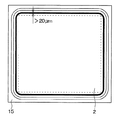
このように、第2の領域に備えられるFWD(200)の幅を20μm以上とすることでFWD(200)のオン電圧を低減することが可能となる。
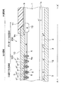
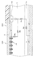
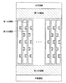
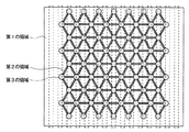
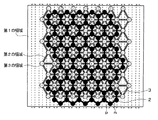
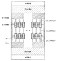
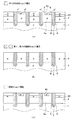
本発明の第1実施形態について説明する。図1は、本実施形態にかかる半導体装置の断面図、図2は、図1に示す半導体装置の上面レイアウト図である。図1は、図2のA−A断面図に相当している。以下、これらの図を参照して、本実施形態の半導体装置について説明する。
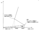
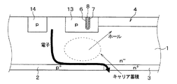
また、スナップバック電圧VSBが最も大きくなる時のVAK1は、FWD200がダイオード動作を行っていることが必要であることから、図4中の点Xの電位に基づいて、次式を導くことができる。なお、下記の式で、Iは、IGBT100からn−型ドリフト層1の内部抵抗R1、R2およびFS層1aの内部抵抗R3を通って流れる電流を意味している。また、下記の式では、IGBT100のチャネル抵抗に関しては、非常に小さいことから無視している。
(数3) I=VAK1・(R1/(R1+R2+R3))
(数4) VAK1=VAK(th)×((R1+R2+R3)/R1)
また、p型ディープウェル層13とn−型ドリフト層1との間のビルトインポテンシャルVAK(th)は、FWD200がダイオード動作し始めた電圧VAK2とほぼ等しいため、次式で表せる。
この数式5および上記した数式4を上記数式1に代入すると、次式を導出することができる。
そして、R1〜R3は、それぞれR1=W2・ρ1/L1、R2=ρ1・L1/W2、R3=W1・ρ2/L2で表されることから、数式6を次式に変換できる。
VSB≒((L1・ρ1/W2+W1・ρ2/L2)/(W2・ρ1/L1))×VAK(th)
ここで、VSB/VAK(th)に対してIGBT100およびFWD200の形状や濃度等、IGBT100およびFWD200の構造に基づいて決まる第1パラメータをk1とし、ビルトインポテンシャルVAK(th)に対するスナップバック電圧VSBの比であるVSB/VAK(th)に対して第1パラメータを掛けた値(=k1・VSB/VAK(th))をKとする。また、ビルトインポテンシャルを表すVAK(th)は定数であり、スナップバック電圧VSBが小さいほど非線形性が小さくなって線形性が改善されることから、Kが小さくなるほど線形性を改善できる。したがって、次式で表される右辺がそのK以下となるようにすることで、線形性の改善を図ることができる。
また、p型ディープウェル層13の外周端部がゲートのバイアスによって影響を受けないダイオードとして動作させるためのW2の条件は、上記数式8に基づいて下記数式9および数式10のように求めることができる。なお、n−型ドリフト層1の抵抗率ρ1に対してFS層1aの抵抗率ρ2は十分に小さいことから、W1・ρ2/L2≒0と見なしている。
(数10) W2≧L1/K1/2
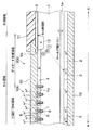
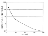
また外周端部におけるスナップバック電圧を−40℃におけるVAK(th)=0.8[V]に対して無視できる0.1V以下にする場合は、実験結果を示した図8よりK≧2.5となる。すなわち、図8中に示しように、L1=135μmとした場合には、W2=85μmのときにスナップバック電圧が0.1Vとなることから、数式9にL1=135μm、W2=85μmを代入すると、K≧2.5となる。同様に、L1=80μmとした場合には、W2=50μmのときにスナップバック電圧が0.1Vとなることから、数式9にL1=80μm、W2=50μmを代入すると、K≧2.56となる。このように、いずれの結果からもK≧2.5を満たすようにすることで、スナップバック電圧を0.1V以下に抑えることが可能となることが判る。なお、図8に示すSim解析では、W1=0μm、L2>0、W3は任意の値に設定している。
(数11) W2−W1≧10μm
一方、距離W3については、図3に示すように、ホールがp型ディープウェル層13から斜め方向に最短距離でp+型不純物領域2とn+型不純物領域3との境界位置に向かってホールが注入された時、注入量が大きくなり破壊しないためには、拡散長よりも上で述べた最短距離が十分大きいことが必要となることから、図4および三角形の関係で示される三平方の定理より、数式12が成り立つ。そして、これを変換すると数式13を導出できる。なお、Dは、n-型ドリフト層1内でのキャリアの拡散係数であり、k2は、p型ディープウェル層13の深さ、濃度、耐量等のp型ディープウェル層13の構造に基づいて決まる第2パラメータである。
(数13) W3≧((k2・(Dτ)1/2)2−L12)^(1/2)
そして、距離W1〜W3については、半導体装置の小型化などを考慮すると、上記数式を満たす中で最も小さい値であることが好ましいため、またW1−W3は耐圧の観点から大きな値となることが望ましいため次式が成り立つ関係とするのが良い。
W2=L1/K1/2
かつ
W2−W1=10μm
かつ
W3=((k2・(Dτ)1/2)2−L12)^(1/2)
よって、本実施形態の半導体装置では、距離W1、W2、W3が数式14を満たす値に設定している。
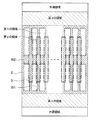
本発明の第2実施形態について説明する。本実施形態は、第1実施形態に対して異なる場所でもFWDのVf−If特性の線形性を改善できる構成を採用したものであり、その他に関しては第1実施形態と同様であるため、第1実施形態と異なる部分についてのみ説明する。
本発明の第3実施形態について説明する。本実施形態は、第2実施形態に対して異なる場所でもFWDのVf−If特性の線形性を改善しつつ、IGBTのオン損失を低減できる構成を採用したものであり、その他に関しては第2実施形態と同様であるため、第2実施形態と異なる部分についてのみ説明する。
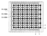
本発明の第4実施形態について説明する。本実施形態は、第2実施形態に対して第1の領域と第2の領域のレイアウトを変更したものであり、その他に関しては第2実施形態と同様であるため、第2実施形態と異なる部分についてのみ説明する。
本発明の第5実施形態について説明する。本実施形態も、第2実施形態に対して第1の領域と第2の領域のレイアウトを変更したものであり、その他に関しては第2実施形態と同様であるため、第2実施形態と異なる部分についてのみ説明する。
本発明の第6実施形態について説明する。本実施形態は、第5実施形態に対して第1の領域と第2の領域のレイアウトを変更したものであり、その他に関しては第5実施形態と同様であるため、第5実施形態と異なる部分についてのみ説明する。
本発明の第7実施形態について説明する。本実施形態は、第6実施形態に対して第1の領域と第2の領域のレイアウトを変更したものであり、その他に関しては第6実施形態と同様であるため、第6実施形態と異なる部分についてのみ説明する。
本発明の第8実施形態について説明する。本実施形態は、第4実施形態に対して第1の領域と第2の領域のレイアウトを変更したものであり、その他に関しては第4実施形態と同様であるため、第4実施形態と異なる部分についてのみ説明する。
本発明の第9実施形態について説明する。本実施形態は、第2実施形態に対して第1〜第3の領域のレイアウトを変更したものであり、その他に関しては第2実施形態と同様であるため、第2実施形態と異なる部分についてのみ説明する。
本発明の第10実施形態について説明する。本実施形態は、第9実施形態に対して第1〜第3の領域のレイアウトを変更したものであり、その他に関しては第9実施形態と同様であるため、第9実施形態と異なる部分についてのみ説明する。
本発明の第11実施形態について説明する。本実施形態も、第9実施形態に対して第1〜第3の領域のレイアウトを変更したものであり、その他に関しては第9実施形態と同様であるため、第9実施形態と異なる部分についてのみ説明する。
本発明の第12実施形態について説明する。本実施形態は、第2実施形態に対して半導体装置の基板裏面側のレイアウトについても考慮したものであり、その他に関しては第2実施形態と同様であるため、第2実施形態と異なる部分についてのみ説明する。
本発明の第13実施形態について説明する。本実施形態は、第12実施形態に対して半導体装置の基板裏面側のレイアウトについても考慮したものであり、その他に関しては第12実施形態と同様であるため、第12実施形態と異なる部分についてのみ説明する。
本発明の第14実施形態について説明する。本実施形態は、第13実施形態に対して半導体装置の基板裏面側のレイアウトについても考慮したものであり、その他に関しては第13実施形態と同様であるため、第13実施形態と異なる部分についてのみ説明する。
本発明の第15実施形態について説明する。本実施形態は、第4実施形態に対して半導体装置の基板裏面側のレイアウトについても考慮したものであり、その他に関しては第4実施形態と同様であるため、第4実施形態と異なる部分についてのみ説明する。
本発明の第16実施形態について説明する。本実施形態は、第9実施形態に対して半導体装置の基板裏面側のレイアウトについても考慮したものであり、その他に関しては第9実施形態と同様であるため、第9実施形態と異なる部分についてのみ説明する。
本発明の第17実施形態について説明する。本実施形態は、第10実施形態に対して半導体装置の基板裏面側のレイアウトについても考慮したものであり、その他に関しては第10実施形態と同様であるため、第10実施形態と異なる部分についてのみ説明する。
本発明の第18実施形態について説明する。本実施形態は、第11実施形態に対して半導体装置の基板裏面側のレイアウトについても考慮したものであり、その他に関しては第11実施形態と同様であるため、第11実施形態と異なる部分についてのみ説明する。
本発明の第19実施形態について説明する。本実施形態は、第12実施形態に対してよりスイッチング損失低減が図れるレイアウトにしたものであり、その他に関しては第12実施形態と同様であるため、第12実施形態と異なる部分についてのみ説明する。
本発明の第20実施形態について説明する。本実施形態は、第12実施形態に対してよりスイッチング損失低減が図れるレイアウトにしたものであり、その他に関しては第12実施形態と同様であるため、第12実施形態と異なる部分についてのみ説明する。
本発明の第21実施形態について説明する。本実施形態は、第20実施形態に対して混在領域15の構造を変更したものであり、その他に関しては第20実施形態と同様であるため、第20実施形態と異なる部分についてのみ説明する。
本発明の第22実施形態について説明する。本実施形態も、第20実施形態に対して混在領域15の構造を変更したものであり、その他に関しては第20実施形態と同様であるため、第20実施形態と異なる部分についてのみ説明する。
本発明の第23実施形態について説明する。本実施形態は、第21実施形態に対して混在領域15の構造を変更したものであり、その他に関しては第21実施形態と同様であるため、第21実施形態と異なる部分についてのみ説明する。
(1)上記各実施形態では、IGBT100とFWD200を備えた半導体装置の一例について説明したが、各構成の形状を変更するなど、適宜変更可能である。例えば、第2〜第23実施形態では、第1〜第3の領域を備えた構造について説明した。また、第4〜第8実施形態において、図中破線で囲んだエミッタ領域に相当するn+型不純物領域5が備えられていない領域を設け、この領域を第2の領域と同じ構造とする場合について説明した。しかしながら、上記各実施形態で説明した構造は単なる一例を示したものであり、第1〜第3の領域の構成や第4〜第8実施形態において図中破線で囲んだ領域の構成を変更しても良い。
2 p+型不純物領域
3 n+型不純物領域
4 p型ベース領域
4a チャネルp層
5 n+型不純物領域
6 トレンチ
7 ゲート絶縁膜
8 ゲート電極
9 層間絶縁膜
10 上部電極
12 下部電極
13 p型ディープウェル層
100 IGBT
200 FWD
Claims (17)
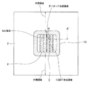
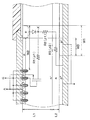
- セル領域に縦型の絶縁ゲート型バイポーラトランジスタ(100)が備えられると共に、該セル領域における前記絶縁ゲート型バイポーラトランジスタ(100)を囲むようにフリーホイールダイオード(200)が備えられ、さらに前記セル領域を囲む外周耐圧構造が形成された外周領域が備えられる半導体装置であって、
第1導電型のドリフト層(1)と、
前記セル領域および前記外周領域において、前記第1導電型のドリフト層(1)の裏面側に配置された第2導電型のコレクタ領域(2)と、
前記セル領域において、前記第1導電型のドリフト層(1)の裏面側における前記コレクタ領域(2)が配置されていない領域に配置された第1導電型のカソード領域(3)と、
前記ドリフト層(1)の表面側の表層部において、前記セル領域のうち前記絶縁ゲート型バイポーラトランジスタ(100)が備えられる領域および前記フリーホイールダイオード(200)が備えられる領域に形成された第2導電型のベース領域(4)と、
前記ベース領域(4)の表層部に形成された第1導電型のエミッタ領域(5)と、
前記エミッタ領域(5)と前記ドリフト層(1)の間における前記ベース領域(4)の表面に形成されたゲート絶縁膜(7)と、
前記ゲート絶縁膜(7)の上に形成されたゲート電極(8)と、
前記ドリフト層(1)の表面側の表層部において、前記セル領域のうち前記フリーホイールダイオード(200)が備えられる領域に形成され、前記ベース領域(4)の外周を囲みつつ、前記ベース領域(4)と接続され、前記ベース領域(4)よりも高不純物濃度で深くされた第2導電型のディープウェル層(13)と、
前記エミッタ領域(5)と前記ベース領域(4)および前記ディープウェル層(13)と電気的に接続された上部電極(10)と、
前記コレクタ領域(2)および前記カソード領域(3)に電気的に接続された下部電極(12)とを有し、
前記ディープウェル層(13)の外周側端部を前記ドリフト層(1)の裏面側に投影した位置より前記カソード領域(3)と前記コレクタ領域(2)との境界部までの距離をW1、前記ベース領域(4)のうち前記絶縁ゲート型バイポーラトランジスタ(100)と前記フリーホイールダイオード(200)との境界部から前記ディープウェル層(13)の外周側端部までの距離をW2、前記ディープウェル層(13)と前記ベース領域(4)との境界部を裏面側に投影した位置より前記カソード領域(3)と前記コレクタ領域(2)との境界部までの距離をW3、前記ドリフト層(1)の厚みをL1、前記ドリフト層(1)内でのキャリアの拡散係数をD、キャリアのライフタイムをτ、前記絶縁ゲート型バイポーラトランジスタ(100)および前記フリーホイールダイオード(200)の構造に基づいて決まる第1パラメータをk1、前記ディープウェル層(13)の構造に基づいて決まる第2パラメータをk2、前記ディープウェル層(13)と前記ドリフト層(1)の間のビルトインポテンシャル(VAK(th))に対するスナップバック電圧(VSB)の比に対して前記第1パラメータk1を掛けた値(k1・VSB/VAK(th))をKとすると、
距離W1と距離W2および距離W3は、
W3≧((k2・(Dτ)1/2)2−L12)^(1/2)
かつ、
W2≧L1/K1/2
ただし、K≧2.5
かつ
W2−W1≧10μm
を満たす値とされていることを特徴とする半導体装置。 - 前記距離W3、W2、W1は、
W3=((k2・(Dτ)1/2)2−L12)^(1/2)
かつ
W2=L1/K1/2
かつ
W2−W1=10μm
であることを特徴とする請求項1に記載の半導体装置。 - 前記ゲート電極(8)が一方向を長手方向として延設されたゲート構造とされ、
前記ゲート構造の長手方向の先端位置においても、
前記距離W1と前記距離W2および前記距離W3は、
W3≧((k2・(Dτ)1/2)2−L12)^(1/2)
かつ、
W2≧L1/K1/2
ただし、K≧2.5
かつ
W2−W1≧10μm
を満たす値とされていることを特徴とする請求項1または2に記載の半導体装置。 - 前記複数のゲート構造の間の一部において、前記エミッタ領域(5)が形成されない部分を備えることにより、前記エミッタ領域(5)が形成されていて前記絶縁ゲート型バイポーラトランジスタ(100)として動作する部分を含む第1の領域と、前記エミッタ領域(5)が形成されない部分を含み、かつ、当該部分が前記フリーホイールダイオード(200)として動作する第2の領域とを構成し、前記絶縁ゲート型バイポーラトランジスタ(100)を囲む前記フリーホイールダイオード(200)が備えられ部分を第3の領域として、
前記第1の領域および前記第2の領域は、前記ゲート構造と同方向が長手方向とされ、
前記第3の領域に加えて前記第2の領域にも前記フリーホイールダイオード(200)を備えた構成とすることを特徴とする請求項3に記載の半導体装置。 - 前記エミッタ領域(5)が形成されない部分の幅が20μm以上とされていることを特徴とする請求項4に記載の半導体装置。
- 前記カソード領域(3)は、前記第1の領域の長手方向と同方向を長手方向として形成されていると共に、前記第1の領域の長手方向先端部よりも突き出して配置されており、該長手方向において分割されていることを特徴とする請求項4または5に記載の半導体装置。
- 前記第1の領域は長手方向において複数に分割されていることを特徴とする請求項4または5に記載の半導体装置。
- 分割された前記第1の領域の間の領域に前記ベース領域(4)のみが形成されることで、当該領域にもフリーホイールダイオード(200)が構成されていることを特徴とする請求項7に記載の半導体装置。
- 前記カソード領域(3)は、前記第1の領域の長手方向と同方向を長手方向として形成されており、
前記第1の領域の長手方向先端部の方が前記カソード領域(3)の長手方向先端部よりも突き出して配置されていることを特徴とする請求項7または8に記載の半導体装置。 - 前記分割された前記第1の領域の間の距離(W、B2)が前記距離W2の2倍以上とされていることを特徴とする請求項7ないし9のいずれか1つに記載の半導体装置。
- 前記第1の領域は、さらに長手方向において複数箇所で分割されており、複数箇所で分割された当該第1の領域の間の領域に前記エミッタ領域(5)が形成されないことで、当該領域にもフリーホイールダイオード(200)が構成され、
前記カソード領域(3)は、複数箇所で分割された前記第1の領域の間の領域と対応する位置において前記第1の領域と対応する位置よりも幅広とされていることを特徴とする請求項7ないし10のいずれか1つに記載の半導体装置。 - 前記第1の領域は複数本並べて配置され、隣り合う当該第1の領域のうち対向する辺の一部が凹まされ、該凹まされた領域にもフリーホイールダイオード(200)が構成されていることを特徴とする請求項4または5に記載の半導体装置。
- 前記カソード領域(3)は、前記第1の領域の長手方向と同方向を長手方向として形成されており、
前記第1の領域の一部が凹まされた領域に設けられた前記フリーホイールダイオード(200)と対向して、当該凹まされた領域に設けられた前記フリーホイールダイオード(200)の幅に合せて前記カソード領域(3)が形成されていることを特徴とする請求項12に記載の半導体装置。 - 前記カソード領域(3)は、前記第2の領域と対応する場所に形成された領域(3a)と、該第2の領域と対応する場所に形成された領域(3a)よりも幅が狭く、かつ、前記第1の領域と対応する場所に形成された領域(3b)とを有していることを特徴とする請求項4ないし13のいずれか1つに記載の半導体装置。
- 前記ドリフト層(1)の裏面側において、前記セル領域の外縁部には、前記コレクタ領域(2)および前記カソード領域(3)が混在する混在領域(15)が備えられていることを特徴とする請求項1ないし14のいずれか1つに記載の半導体装置。
- 前記セル領域および前記外周領域において、前記第1導電型のドリフト層(1)の裏面側に配置され、前記ドリフト層(1)よりも高不純物濃度とされた第1導電型のフィールドストップ層(1a)を有し、
前記コレクタ領域(2)および前記カソード領域(3)は、前記ドリフト層(1)の裏面側における前記フィールドストップ層(1a)の表層部に形成されていることを特徴とする請求項1ないし15のいずれか1つに記載の半導体装置。 - 前記ベース領域(4)を貫通し、一方向を長手方向として複数本が所定の間隔で並べられたトレンチ(6)を有し、
前記ゲート絶縁膜(7)および前記ゲート電極(8)が前記トレンチ(6)内において形成されたトレンチゲート構造であることを特徴とする請求項1ないし16のいずれか1つに記載の半導体装置。
Priority Applications (6)
| Application Number | Priority Date | Filing Date | Title |
|---|---|---|---|
| JP2011139567A JP5582102B2 (ja) | 2010-07-01 | 2011-06-23 | 半導体装置 |
| US13/805,740 US8847276B2 (en) | 2010-07-01 | 2011-06-29 | Semiconductor device |
| DE112011102263T DE112011102263T5 (de) | 2010-07-01 | 2011-06-29 | Halbleitervorrichtung |
| CN201180032538.5A CN102959705B (zh) | 2010-07-01 | 2011-06-29 | 半导体器件 |
| PCT/JP2011/003718 WO2012001967A1 (ja) | 2010-07-01 | 2011-06-29 | 半導体装置 |
| US14/468,602 US9224730B2 (en) | 2010-07-01 | 2014-08-26 | Semiconductor device |
Applications Claiming Priority (3)
| Application Number | Priority Date | Filing Date | Title |
|---|---|---|---|
| JP2010151235 | 2010-07-01 | ||
| JP2010151235 | 2010-07-01 | ||
| JP2011139567A JP5582102B2 (ja) | 2010-07-01 | 2011-06-23 | 半導体装置 |
Related Child Applications (1)
| Application Number | Title | Priority Date | Filing Date |
|---|---|---|---|
| JP2014146907A Division JP5900546B2 (ja) | 2010-07-01 | 2014-07-17 | 半導体装置 |
Publications (2)
| Publication Number | Publication Date |
|---|---|
| JP2012033897A JP2012033897A (ja) | 2012-02-16 |
| JP5582102B2 true JP5582102B2 (ja) | 2014-09-03 |
Family
ID=45401707
Family Applications (1)
| Application Number | Title | Priority Date | Filing Date |
|---|---|---|---|
| JP2011139567A Active JP5582102B2 (ja) | 2010-07-01 | 2011-06-23 | 半導体装置 |
Country Status (5)
| Country | Link |
|---|---|
| US (2) | US8847276B2 (ja) |
| JP (1) | JP5582102B2 (ja) |
| CN (1) | CN102959705B (ja) |
| DE (1) | DE112011102263T5 (ja) |
| WO (1) | WO2012001967A1 (ja) |
Families Citing this family (45)
| Publication number | Priority date | Publication date | Assignee | Title |
|---|---|---|---|---|
| JP5582102B2 (ja) * | 2010-07-01 | 2014-09-03 | 株式会社デンソー | 半導体装置 |
| JP6022774B2 (ja) * | 2012-01-24 | 2016-11-09 | トヨタ自動車株式会社 | 半導体装置 |
| JP2014103376A (ja) | 2012-09-24 | 2014-06-05 | Toshiba Corp | 半導体装置 |
| CN103839993A (zh) * | 2012-11-23 | 2014-06-04 | 中国科学院微电子研究所 | 用于绝缘栅双极晶体管的防闩锁终端区 |
| CN102983077B (zh) * | 2012-12-06 | 2015-10-14 | 乐山嘉洋科技发展有限公司 | 一种二极管芯片的制备方法 |
| US9111989B2 (en) | 2013-03-26 | 2015-08-18 | Infineon Technologies Austria Ag | Insulated gate bipolar transistor including emitter short regions |
| CN103208531B (zh) * | 2013-04-07 | 2015-07-15 | 株洲南车时代电气股份有限公司 | 一种快恢复二极管frd芯片及其制作方法 |
| JP2014241367A (ja) * | 2013-06-12 | 2014-12-25 | 三菱電機株式会社 | 半導体素子、半導体素子の製造方法 |
| CN104347708A (zh) * | 2013-08-07 | 2015-02-11 | 中芯国际集成电路制造(北京)有限公司 | 多栅vdmos晶体管及其形成方法 |
| US9147727B2 (en) * | 2013-09-30 | 2015-09-29 | Infineon Technologies Ag | Semiconductor device and method for forming a semiconductor device |
| US10361191B2 (en) * | 2014-08-26 | 2019-07-23 | Mitsubishi Electric Corporation | Semiconductor device |
| JP6261494B2 (ja) * | 2014-12-03 | 2018-01-17 | 三菱電機株式会社 | 電力用半導体装置 |
| JP6269860B2 (ja) * | 2014-12-17 | 2018-01-31 | 三菱電機株式会社 | 半導体装置 |
| JP6641983B2 (ja) * | 2015-01-16 | 2020-02-05 | 株式会社デンソー | 半導体装置 |
| WO2016129041A1 (ja) * | 2015-02-09 | 2016-08-18 | 三菱電機株式会社 | 半導体装置 |
| JP6319151B2 (ja) | 2015-03-23 | 2018-05-09 | 豊田合成株式会社 | 半導体装置および半導体装置の製造方法 |
| CN107683530B (zh) * | 2015-06-09 | 2020-08-18 | 三菱电机株式会社 | 电力用半导体装置 |
| JP6334465B2 (ja) * | 2015-06-17 | 2018-05-30 | 富士電機株式会社 | 半導体装置 |
| DE102015111371B4 (de) | 2015-07-14 | 2017-07-20 | Infineon Technologies Ag | Halbleiterbauelement mit einem schaltbaren und einem nicht schaltbaren Diodengebiet |
| CN105023943B (zh) * | 2015-08-10 | 2018-01-09 | 电子科技大学 | 一种纵向rc‑igbt器件 |
| JP6445952B2 (ja) * | 2015-10-19 | 2018-12-26 | 株式会社東芝 | 半導体装置 |
| JP6260605B2 (ja) | 2015-11-19 | 2018-01-17 | トヨタ自動車株式会社 | 半導体装置 |
| CN107086217B (zh) * | 2016-02-16 | 2023-05-16 | 富士电机株式会社 | 半导体装置 |
| JP6878848B2 (ja) * | 2016-02-16 | 2021-06-02 | 富士電機株式会社 | 半導体装置 |
| JP6846119B2 (ja) * | 2016-05-02 | 2021-03-24 | 株式会社 日立パワーデバイス | ダイオード、およびそれを用いた電力変換装置 |
| JP2017208413A (ja) * | 2016-05-17 | 2017-11-24 | 株式会社デンソー | 半導体装置 |
| JP6830767B2 (ja) | 2016-06-14 | 2021-02-17 | 株式会社デンソー | 半導体装置 |
| JP6854598B2 (ja) | 2016-07-06 | 2021-04-07 | ローム株式会社 | 半導体装置 |
| JP6801324B2 (ja) * | 2016-09-15 | 2020-12-16 | 富士電機株式会社 | 半導体装置 |
| DE102016117723A1 (de) * | 2016-09-20 | 2018-03-22 | Infineon Technologies Ag | Diodenstruktur eines Leistungshalbleiterbauelements |
| CN109314134B (zh) | 2016-12-16 | 2021-11-05 | 富士电机株式会社 | 半导体装置及制造方法 |
| JP6854654B2 (ja) * | 2017-01-26 | 2021-04-07 | ローム株式会社 | 半導体装置 |
| JP6624101B2 (ja) | 2017-02-03 | 2019-12-25 | 株式会社デンソー | 半導体装置 |
| US10439038B2 (en) | 2017-02-09 | 2019-10-08 | Kabushiki Kaisha Toshiba | Semiconductor device and electrical apparatus |
| CN108417549B (zh) | 2017-02-09 | 2021-09-24 | 株式会社东芝 | 半导体装置及电气设备 |
| JP6824135B2 (ja) * | 2017-09-29 | 2021-02-03 | 三菱電機株式会社 | 半導体装置及びその製造方法 |
| JP6935731B2 (ja) * | 2017-11-16 | 2021-09-15 | 株式会社デンソー | 半導体装置 |
| JP6935351B2 (ja) * | 2018-03-20 | 2021-09-15 | 株式会社東芝 | 半導体装置 |
| CN109728085B (zh) * | 2018-12-29 | 2021-10-22 | 安建科技(深圳)有限公司 | 一种逆导型绝缘栅双极性晶体管 |
| WO2020202430A1 (ja) * | 2019-04-01 | 2020-10-08 | 三菱電機株式会社 | 半導体装置 |
| DE112020002890T5 (de) | 2020-01-17 | 2022-02-24 | Fuji Electric Co., Ltd. | Halbleitervorrichtung |
| JP7332543B2 (ja) * | 2020-07-07 | 2023-08-23 | 三菱電機株式会社 | 半導体装置 |
| EP4199100A1 (en) * | 2021-12-20 | 2023-06-21 | Hitachi Energy Switzerland AG | Reverse-conducting insulated gate bipolar transistor |
| JP7821710B2 (ja) * | 2022-09-21 | 2026-02-27 | ルネサスエレクトロニクス株式会社 | 半導体装置 |
| CN117954482A (zh) * | 2023-10-31 | 2024-04-30 | 海信家电集团股份有限公司 | 半导体装置 |
Family Cites Families (19)
| Publication number | Priority date | Publication date | Assignee | Title |
|---|---|---|---|---|
| JPH06196705A (ja) | 1992-12-24 | 1994-07-15 | Hitachi Ltd | 逆導通型絶縁ゲートバイポーラトランジスタ及びその製造方法 |
| JPH08102536A (ja) * | 1994-09-30 | 1996-04-16 | Sanyo Electric Co Ltd | 絶縁ゲート型半導体装置 |
| JPH08274310A (ja) | 1995-03-29 | 1996-10-18 | Sanyo Electric Co Ltd | 絶縁ゲート型半導体装置 |
| US6204717B1 (en) | 1995-05-22 | 2001-03-20 | Hitachi, Ltd. | Semiconductor circuit and semiconductor device for use in equipment such as a power converting apparatus |
| JP4351745B2 (ja) | 1997-09-19 | 2009-10-28 | 株式会社東芝 | 半導体装置 |
| JP2001196606A (ja) | 2000-01-11 | 2001-07-19 | Mitsubishi Electric Corp | ダイオード |
| JP4799829B2 (ja) | 2003-08-27 | 2011-10-26 | 三菱電機株式会社 | 絶縁ゲート型トランジスタ及びインバータ回路 |
| JP5011748B2 (ja) | 2006-02-24 | 2012-08-29 | 株式会社デンソー | 半導体装置 |
| JP5157201B2 (ja) * | 2006-03-22 | 2013-03-06 | 株式会社デンソー | 半導体装置 |
| JP2007258363A (ja) | 2006-03-22 | 2007-10-04 | Denso Corp | 半導体装置 |
| JP5103830B2 (ja) | 2006-08-28 | 2012-12-19 | 三菱電機株式会社 | 絶縁ゲート型半導体装置 |
| DE102008045410B4 (de) | 2007-09-05 | 2019-07-11 | Denso Corporation | Halbleitervorrichtung mit IGBT mit eingebauter Diode und Halbleitervorrichtung mit DMOS mit eingebauter Diode |
| JP5206541B2 (ja) | 2008-04-01 | 2013-06-12 | 株式会社デンソー | 半導体装置およびその製造方法 |
| JP4743447B2 (ja) | 2008-05-23 | 2011-08-10 | 三菱電機株式会社 | 半導体装置 |
| JP5045733B2 (ja) * | 2008-12-24 | 2012-10-10 | 株式会社デンソー | 半導体装置 |
| JP5280190B2 (ja) | 2008-12-25 | 2013-09-04 | 川崎重工業株式会社 | 磁気軸受制御装置 |
| JP5366297B2 (ja) * | 2009-02-10 | 2013-12-11 | 富士電機株式会社 | 半導体装置 |
| JP2011139567A (ja) | 2009-12-28 | 2011-07-14 | Sanyo Electric Co Ltd | 駆動制御装置及びこれを搭載した電動車両 |
| JP5582102B2 (ja) * | 2010-07-01 | 2014-09-03 | 株式会社デンソー | 半導体装置 |
-
2011
- 2011-06-23 JP JP2011139567A patent/JP5582102B2/ja active Active
- 2011-06-29 CN CN201180032538.5A patent/CN102959705B/zh active Active
- 2011-06-29 DE DE112011102263T patent/DE112011102263T5/de not_active Withdrawn
- 2011-06-29 WO PCT/JP2011/003718 patent/WO2012001967A1/ja not_active Ceased
- 2011-06-29 US US13/805,740 patent/US8847276B2/en active Active
-
2014
- 2014-08-26 US US14/468,602 patent/US9224730B2/en active Active
Also Published As
| Publication number | Publication date |
|---|---|
| WO2012001967A1 (ja) | 2012-01-05 |
| US8847276B2 (en) | 2014-09-30 |
| JP2012033897A (ja) | 2012-02-16 |
| DE112011102263T5 (de) | 2013-06-06 |
| CN102959705A (zh) | 2013-03-06 |
| US20130087829A1 (en) | 2013-04-11 |
| CN102959705B (zh) | 2015-11-25 |
| US20140361334A1 (en) | 2014-12-11 |
| US9224730B2 (en) | 2015-12-29 |
Similar Documents
| Publication | Publication Date | Title |
|---|---|---|
| JP5582102B2 (ja) | 半導体装置 | |
| JP5900546B2 (ja) | 半導体装置 | |
| JP5216801B2 (ja) | 半導体装置 | |
| CN109964317B (zh) | 半导体装置 | |
| CN107086217B (zh) | 半导体装置 | |
| JP4957840B2 (ja) | 絶縁ゲート型半導体装置 | |
| US11217580B2 (en) | Semiconductor device including insulated gate bipolar transistor element and freewheeling diode element | |
| JP6673499B2 (ja) | 半導体装置 | |
| JP7533684B2 (ja) | 半導体装置 | |
| JP2017147435A (ja) | 半導体装置 | |
| JP2008288386A (ja) | 半導体装置 | |
| JP2009026797A (ja) | 半導体装置 | |
| JP2013065735A (ja) | 半導体装置 | |
| JP2009188178A (ja) | 半導体装置 | |
| CN108417614A (zh) | 半导体装置 | |
| JP5678469B2 (ja) | 半導体装置 | |
| CN110140220B (zh) | 半导体装置 | |
| JP2015181178A (ja) | 半導体装置 | |
| JP2013145903A (ja) | 半導体装置 | |
| JP5167741B2 (ja) | 半導体装置 | |
| EP1883971B1 (en) | Cathode cell design | |
| JP4821086B2 (ja) | 半導体装置 | |
| JP5261893B2 (ja) | トレンチ型絶縁ゲートバイポーラトランジスタ | |
| JP5698302B2 (ja) | 半導体装置 | |
| JP5186869B2 (ja) | 半導体装置 |
Legal Events
| Date | Code | Title | Description |
|---|---|---|---|
| A621 | Written request for application examination |
Free format text: JAPANESE INTERMEDIATE CODE: A621 Effective date: 20120611 |
|
| A131 | Notification of reasons for refusal |
Free format text: JAPANESE INTERMEDIATE CODE: A131 Effective date: 20131217 |
|
| A521 | Request for written amendment filed |
Free format text: JAPANESE INTERMEDIATE CODE: A523 Effective date: 20140213 |
|
| TRDD | Decision of grant or rejection written | ||
| A01 | Written decision to grant a patent or to grant a registration (utility model) |
Free format text: JAPANESE INTERMEDIATE CODE: A01 Effective date: 20140617 |
|
| A61 | First payment of annual fees (during grant procedure) |
Free format text: JAPANESE INTERMEDIATE CODE: A61 Effective date: 20140630 |
|
| R151 | Written notification of patent or utility model registration |
Ref document number: 5582102 Country of ref document: JP Free format text: JAPANESE INTERMEDIATE CODE: R151 |
|
| R250 | Receipt of annual fees |
Free format text: JAPANESE INTERMEDIATE CODE: R250 |
|
| R250 | Receipt of annual fees |
Free format text: JAPANESE INTERMEDIATE CODE: R250 |
|
| R250 | Receipt of annual fees |
Free format text: JAPANESE INTERMEDIATE CODE: R250 |
|
| R250 | Receipt of annual fees |
Free format text: JAPANESE INTERMEDIATE CODE: R250 |
|
| R250 | Receipt of annual fees |
Free format text: JAPANESE INTERMEDIATE CODE: R250 |
|
| R250 | Receipt of annual fees |
Free format text: JAPANESE INTERMEDIATE CODE: R250 |
|
| R250 | Receipt of annual fees |
Free format text: JAPANESE INTERMEDIATE CODE: R250 |
|
| R250 | Receipt of annual fees |
Free format text: JAPANESE INTERMEDIATE CODE: R250 |
|
| R250 | Receipt of annual fees |
Free format text: JAPANESE INTERMEDIATE CODE: R250 |