JP5582102B2 - Semiconductor device - Google Patents
Semiconductor device Download PDFInfo
- Publication number
- JP5582102B2 JP5582102B2 JP2011139567A JP2011139567A JP5582102B2 JP 5582102 B2 JP5582102 B2 JP 5582102B2 JP 2011139567 A JP2011139567 A JP 2011139567A JP 2011139567 A JP2011139567 A JP 2011139567A JP 5582102 B2 JP5582102 B2 JP 5582102B2
- Authority
- JP
- Japan
- Prior art keywords
- region
- semiconductor device
- longitudinal direction
- fwd
- type impurity
- Prior art date
- Legal status (The legal status is an assumption and is not a legal conclusion. Google has not performed a legal analysis and makes no representation as to the accuracy of the status listed.)
- Active
Links
- 239000004065 semiconductor Substances 0.000 title claims description 134
- 239000012535 impurity Substances 0.000 claims description 148
- 239000010410 layer Substances 0.000 claims description 136
- 230000002093 peripheral effect Effects 0.000 claims description 27
- 238000009792 diffusion process Methods 0.000 claims description 14
- 239000002344 surface layer Substances 0.000 claims description 12
- 239000000969 carrier Substances 0.000 claims description 6
- 230000000149 penetrating effect Effects 0.000 claims description 2
- 238000010586 diagram Methods 0.000 description 49
- 239000000758 substrate Substances 0.000 description 24
- 230000014509 gene expression Effects 0.000 description 19
- DBWPFHJYSTVBCZ-BYPYZUCNSA-N 3-(5-fluorouracil-1-yl)-L-alanine Chemical compound OC(=O)[C@@H](N)CN1C=C(F)C(=O)NC1=O DBWPFHJYSTVBCZ-BYPYZUCNSA-N 0.000 description 18
- 230000012447 hatching Effects 0.000 description 18
- 230000015572 biosynthetic process Effects 0.000 description 13
- 230000000694 effects Effects 0.000 description 13
- 108091006146 Channels Proteins 0.000 description 11
- 230000009467 reduction Effects 0.000 description 11
- RUCNAYOMFXRIKJ-DCAQKATOSA-N Val-Ala-Lys Chemical compound CC(C)[C@H](N)C(=O)N[C@@H](C)C(=O)N[C@H](C(O)=O)CCCCN RUCNAYOMFXRIKJ-DCAQKATOSA-N 0.000 description 10
- 238000002347 injection Methods 0.000 description 7
- 239000007924 injection Substances 0.000 description 7
- 239000011159 matrix material Substances 0.000 description 3
- 230000003071 parasitic effect Effects 0.000 description 3
- 230000015556 catabolic process Effects 0.000 description 2
- 238000006243 chemical reaction Methods 0.000 description 2
- 230000007423 decrease Effects 0.000 description 2
- 238000010894 electron beam technology Methods 0.000 description 2
- 239000011229 interlayer Substances 0.000 description 2
- 238000011084 recovery Methods 0.000 description 2
- 238000010992 reflux Methods 0.000 description 2
- ZOXJGFHDIHLPTG-UHFFFAOYSA-N Boron Chemical compound [B] ZOXJGFHDIHLPTG-UHFFFAOYSA-N 0.000 description 1
- 108010075750 P-Type Calcium Channels Proteins 0.000 description 1
- OAICVXFJPJFONN-UHFFFAOYSA-N Phosphorus Chemical compound [P] OAICVXFJPJFONN-UHFFFAOYSA-N 0.000 description 1
- 229910052796 boron Inorganic materials 0.000 description 1
- 230000000052 comparative effect Effects 0.000 description 1
- 230000005684 electric field Effects 0.000 description 1
- 238000002474 experimental method Methods 0.000 description 1
- 238000005259 measurement Methods 0.000 description 1
- 230000007246 mechanism Effects 0.000 description 1
- 230000004048 modification Effects 0.000 description 1
- 238000012986 modification Methods 0.000 description 1
- 229910052698 phosphorus Inorganic materials 0.000 description 1
- 239000011574 phosphorus Substances 0.000 description 1
- 229910021420 polycrystalline silicon Inorganic materials 0.000 description 1
- 230000001681 protective effect Effects 0.000 description 1
- 230000000630 rising effect Effects 0.000 description 1
- 230000007480 spreading Effects 0.000 description 1
Images


Classifications
-
- H—ELECTRICITY
- H01—ELECTRIC ELEMENTS
- H01L—SEMICONDUCTOR DEVICES NOT COVERED BY CLASS H10
- H01L27/00—Devices consisting of a plurality of semiconductor or other solid-state components formed in or on a common substrate
- H01L27/02—Devices consisting of a plurality of semiconductor or other solid-state components formed in or on a common substrate including semiconductor components specially adapted for rectifying, oscillating, amplifying or switching and having at least one potential-jump barrier or surface barrier; including integrated passive circuit elements with at least one potential-jump barrier or surface barrier
- H01L27/04—Devices consisting of a plurality of semiconductor or other solid-state components formed in or on a common substrate including semiconductor components specially adapted for rectifying, oscillating, amplifying or switching and having at least one potential-jump barrier or surface barrier; including integrated passive circuit elements with at least one potential-jump barrier or surface barrier the substrate being a semiconductor body
- H01L27/06—Devices consisting of a plurality of semiconductor or other solid-state components formed in or on a common substrate including semiconductor components specially adapted for rectifying, oscillating, amplifying or switching and having at least one potential-jump barrier or surface barrier; including integrated passive circuit elements with at least one potential-jump barrier or surface barrier the substrate being a semiconductor body including a plurality of individual components in a non-repetitive configuration
- H01L27/0611—Devices consisting of a plurality of semiconductor or other solid-state components formed in or on a common substrate including semiconductor components specially adapted for rectifying, oscillating, amplifying or switching and having at least one potential-jump barrier or surface barrier; including integrated passive circuit elements with at least one potential-jump barrier or surface barrier the substrate being a semiconductor body including a plurality of individual components in a non-repetitive configuration integrated circuits having a two-dimensional layout of components without a common active region
- H01L27/0641—Devices consisting of a plurality of semiconductor or other solid-state components formed in or on a common substrate including semiconductor components specially adapted for rectifying, oscillating, amplifying or switching and having at least one potential-jump barrier or surface barrier; including integrated passive circuit elements with at least one potential-jump barrier or surface barrier the substrate being a semiconductor body including a plurality of individual components in a non-repetitive configuration integrated circuits having a two-dimensional layout of components without a common active region without components of the field effect type
- H01L27/0647—Bipolar transistors in combination with diodes, or capacitors, or resistors, e.g. vertical bipolar transistor and bipolar lateral transistor and resistor
- H01L27/0652—Vertical bipolar transistor in combination with diodes, or capacitors, or resistors
- H01L27/0664—Vertical bipolar transistor in combination with diodes
-
- H—ELECTRICITY
- H01—ELECTRIC ELEMENTS
- H01L—SEMICONDUCTOR DEVICES NOT COVERED BY CLASS H10
- H01L29/00—Semiconductor devices adapted for rectifying, amplifying, oscillating or switching, or capacitors or resistors with at least one potential-jump barrier or surface barrier, e.g. PN junction depletion layer or carrier concentration layer; Details of semiconductor bodies or of electrodes thereof ; Multistep manufacturing processes therefor
- H01L29/66—Types of semiconductor device ; Multistep manufacturing processes therefor
- H01L29/66007—Multistep manufacturing processes
- H01L29/66075—Multistep manufacturing processes of devices having semiconductor bodies comprising group 14 or group 13/15 materials
- H01L29/66227—Multistep manufacturing processes of devices having semiconductor bodies comprising group 14 or group 13/15 materials the devices being controllable only by the electric current supplied or the electric potential applied, to an electrode which does not carry the current to be rectified, amplified or switched, e.g. three-terminal devices
- H01L29/66234—Bipolar junction transistors [BJT]
- H01L29/66325—Bipolar junction transistors [BJT] controlled by field-effect, e.g. insulated gate bipolar transistors [IGBT]
- H01L29/66333—Vertical insulated gate bipolar transistors
- H01L29/66348—Vertical insulated gate bipolar transistors with a recessed gate
-
- H—ELECTRICITY
- H01—ELECTRIC ELEMENTS
- H01L—SEMICONDUCTOR DEVICES NOT COVERED BY CLASS H10
- H01L27/00—Devices consisting of a plurality of semiconductor or other solid-state components formed in or on a common substrate
- H01L27/02—Devices consisting of a plurality of semiconductor or other solid-state components formed in or on a common substrate including semiconductor components specially adapted for rectifying, oscillating, amplifying or switching and having at least one potential-jump barrier or surface barrier; including integrated passive circuit elements with at least one potential-jump barrier or surface barrier
- H01L27/04—Devices consisting of a plurality of semiconductor or other solid-state components formed in or on a common substrate including semiconductor components specially adapted for rectifying, oscillating, amplifying or switching and having at least one potential-jump barrier or surface barrier; including integrated passive circuit elements with at least one potential-jump barrier or surface barrier the substrate being a semiconductor body
- H01L27/06—Devices consisting of a plurality of semiconductor or other solid-state components formed in or on a common substrate including semiconductor components specially adapted for rectifying, oscillating, amplifying or switching and having at least one potential-jump barrier or surface barrier; including integrated passive circuit elements with at least one potential-jump barrier or surface barrier the substrate being a semiconductor body including a plurality of individual components in a non-repetitive configuration
- H01L27/07—Devices consisting of a plurality of semiconductor or other solid-state components formed in or on a common substrate including semiconductor components specially adapted for rectifying, oscillating, amplifying or switching and having at least one potential-jump barrier or surface barrier; including integrated passive circuit elements with at least one potential-jump barrier or surface barrier the substrate being a semiconductor body including a plurality of individual components in a non-repetitive configuration the components having an active region in common
- H01L27/0705—Devices consisting of a plurality of semiconductor or other solid-state components formed in or on a common substrate including semiconductor components specially adapted for rectifying, oscillating, amplifying or switching and having at least one potential-jump barrier or surface barrier; including integrated passive circuit elements with at least one potential-jump barrier or surface barrier the substrate being a semiconductor body including a plurality of individual components in a non-repetitive configuration the components having an active region in common comprising components of the field effect type
- H01L27/0711—Devices consisting of a plurality of semiconductor or other solid-state components formed in or on a common substrate including semiconductor components specially adapted for rectifying, oscillating, amplifying or switching and having at least one potential-jump barrier or surface barrier; including integrated passive circuit elements with at least one potential-jump barrier or surface barrier the substrate being a semiconductor body including a plurality of individual components in a non-repetitive configuration the components having an active region in common comprising components of the field effect type in combination with bipolar transistors and diodes, or capacitors, or resistors
- H01L27/0722—Devices consisting of a plurality of semiconductor or other solid-state components formed in or on a common substrate including semiconductor components specially adapted for rectifying, oscillating, amplifying or switching and having at least one potential-jump barrier or surface barrier; including integrated passive circuit elements with at least one potential-jump barrier or surface barrier the substrate being a semiconductor body including a plurality of individual components in a non-repetitive configuration the components having an active region in common comprising components of the field effect type in combination with bipolar transistors and diodes, or capacitors, or resistors in combination with lateral bipolar transistors and diodes, or capacitors, or resistors
-
- H—ELECTRICITY
- H01—ELECTRIC ELEMENTS
- H01L—SEMICONDUCTOR DEVICES NOT COVERED BY CLASS H10
- H01L29/00—Semiconductor devices adapted for rectifying, amplifying, oscillating or switching, or capacitors or resistors with at least one potential-jump barrier or surface barrier, e.g. PN junction depletion layer or carrier concentration layer; Details of semiconductor bodies or of electrodes thereof ; Multistep manufacturing processes therefor
- H01L29/40—Electrodes ; Multistep manufacturing processes therefor
- H01L29/41—Electrodes ; Multistep manufacturing processes therefor characterised by their shape, relative sizes or dispositions
- H01L29/423—Electrodes ; Multistep manufacturing processes therefor characterised by their shape, relative sizes or dispositions not carrying the current to be rectified, amplified or switched
- H01L29/42312—Gate electrodes for field effect devices
- H01L29/42316—Gate electrodes for field effect devices for field-effect transistors
- H01L29/4232—Gate electrodes for field effect devices for field-effect transistors with insulated gate
- H01L29/42356—Disposition, e.g. buried gate electrode
- H01L29/4236—Disposition, e.g. buried gate electrode within a trench, e.g. trench gate electrode, groove gate electrode
-
- H—ELECTRICITY
- H01—ELECTRIC ELEMENTS
- H01L—SEMICONDUCTOR DEVICES NOT COVERED BY CLASS H10
- H01L29/00—Semiconductor devices adapted for rectifying, amplifying, oscillating or switching, or capacitors or resistors with at least one potential-jump barrier or surface barrier, e.g. PN junction depletion layer or carrier concentration layer; Details of semiconductor bodies or of electrodes thereof ; Multistep manufacturing processes therefor
- H01L29/66—Types of semiconductor device ; Multistep manufacturing processes therefor
- H01L29/68—Types of semiconductor device ; Multistep manufacturing processes therefor controllable by only the electric current supplied, or only the electric potential applied, to an electrode which does not carry the current to be rectified, amplified or switched
- H01L29/70—Bipolar devices
- H01L29/72—Transistor-type devices, i.e. able to continuously respond to applied control signals
- H01L29/739—Transistor-type devices, i.e. able to continuously respond to applied control signals controlled by field-effect, e.g. bipolar static induction transistors [BSIT]
- H01L29/7393—Insulated gate bipolar mode transistors, i.e. IGBT; IGT; COMFET
- H01L29/7395—Vertical transistors, e.g. vertical IGBT
- H01L29/7396—Vertical transistors, e.g. vertical IGBT with a non planar surface, e.g. with a non planar gate or with a trench or recess or pillar in the surface of the emitter, base or collector region for improving current density or short circuiting the emitter and base regions
- H01L29/7397—Vertical transistors, e.g. vertical IGBT with a non planar surface, e.g. with a non planar gate or with a trench or recess or pillar in the surface of the emitter, base or collector region for improving current density or short circuiting the emitter and base regions and a gate structure lying on a slanted or vertical surface or formed in a groove, e.g. trench gate IGBT
-
- H—ELECTRICITY
- H01—ELECTRIC ELEMENTS
- H01L—SEMICONDUCTOR DEVICES NOT COVERED BY CLASS H10
- H01L29/00—Semiconductor devices adapted for rectifying, amplifying, oscillating or switching, or capacitors or resistors with at least one potential-jump barrier or surface barrier, e.g. PN junction depletion layer or carrier concentration layer; Details of semiconductor bodies or of electrodes thereof ; Multistep manufacturing processes therefor
- H01L29/66—Types of semiconductor device ; Multistep manufacturing processes therefor
- H01L29/86—Types of semiconductor device ; Multistep manufacturing processes therefor controllable only by variation of the electric current supplied, or only the electric potential applied, to one or more of the electrodes carrying the current to be rectified, amplified, oscillated or switched
- H01L29/861—Diodes
-
- H—ELECTRICITY
- H01—ELECTRIC ELEMENTS
- H01L—SEMICONDUCTOR DEVICES NOT COVERED BY CLASS H10
- H01L29/00—Semiconductor devices adapted for rectifying, amplifying, oscillating or switching, or capacitors or resistors with at least one potential-jump barrier or surface barrier, e.g. PN junction depletion layer or carrier concentration layer; Details of semiconductor bodies or of electrodes thereof ; Multistep manufacturing processes therefor
- H01L29/02—Semiconductor bodies ; Multistep manufacturing processes therefor
- H01L29/06—Semiconductor bodies ; Multistep manufacturing processes therefor characterised by their shape; characterised by the shapes, relative sizes, or dispositions of the semiconductor regions ; characterised by the concentration or distribution of impurities within semiconductor regions
- H01L29/0684—Semiconductor bodies ; Multistep manufacturing processes therefor characterised by their shape; characterised by the shapes, relative sizes, or dispositions of the semiconductor regions ; characterised by the concentration or distribution of impurities within semiconductor regions characterised by the shape, relative sizes or dispositions of the semiconductor regions or junctions between the regions
- H01L29/0692—Surface layout
- H01L29/0696—Surface layout of cellular field-effect devices, e.g. multicellular DMOS transistors or IGBTs
Description
本発明は、スイッチング素子として機能する絶縁ゲート型バイポーラトランジスタ(以下、IGBTという)とフリーホイールダイオード(以下、FWDという)とが同一チップ内に集積化された半導体装置に関するものである。 The present invention relates to a semiconductor device in which an insulated gate bipolar transistor (hereinafter referred to as IGBT) and a free wheel diode (hereinafter referred to as FWD) functioning as a switching element are integrated in the same chip.
従来より、直流−交流変換を行うためのインバータ回路などでは、スイッチング素子として機能するIGBTとFWDとが同一チップ内に集積化された半導体装置が使用されている。IGBTのオンオフによって直流−交流交換を行うと共に、IGBTをオフしたときに、FWDを通じて負荷(例えばモータ)に流れる電流を還流させている。 Conventionally, in an inverter circuit or the like for performing DC-AC conversion, a semiconductor device in which IGBT and FWD functioning as switching elements are integrated in the same chip is used. DC-AC exchange is performed by turning on and off the IGBT, and when the IGBT is turned off, a current flowing through a load (for example, a motor) is returned through the FWD.
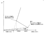
このような半導体装置に使用されるFWDでは、IGBTがオフしているときの順方向電圧Vfに対する順方向電流Ifの特性(以下、Vf−If特性という)は線形となるが、IGBTをオンしたときのVf−If特性はスナップバック電圧の影響により非線形な領域が発生する。図6は、FWDのVf−If特性を示した図である。この図に示されるように、IGBTがオンしたときにはオフしているときと比較して順方向電圧Vfが変動すると共に、スナップバック電圧が発生する領域があり、線形性が得られない。 In the FWD used in such a semiconductor device, the forward current If characteristic with respect to the forward voltage Vf when the IGBT is off (hereinafter referred to as Vf-If characteristic) is linear, but the IGBT is turned on. In the Vf-If characteristic, a non-linear region occurs due to the influence of the snapback voltage. FIG. 6 is a diagram showing Vf-If characteristics of FWD. As shown in this figure, when the IGBT is turned on, the forward voltage Vf fluctuates as compared with when the IGBT is turned off, and there is a region where a snapback voltage is generated, and linearity cannot be obtained.
具体的には、IGBTとFWDとを1チップに形成した半導体装置の場合、IGBTをオンしたときの等価回路図は、図7のように示される。すなわち、p型ディープウェル層13とn−型ドリフト層1にて構成されるFWD200に対してIGBT100のチャネル抵抗RaとチャネルからFWD200のPN接合部(p型ディープウェル層13の下部)に至るまでの内部抵抗Rbとが並列的に接続され、さらにこれらにp型ディープウェル層13の下部におけるn−型ドリフト層1の内部抵抗Rcとフィールドストップ(以下、FSという)層1aの内部抵抗Rdを直列的に接続した状態となる。このような回路において、IGBT100がオンすると、内部抵抗Rbが小さいことからダイオード側よりもIGBT100のチャネル側にばかり電流が流れるため、伝導度変調が起きず、順方向電圧Vfが増大してしまう。
Specifically, in the case of a semiconductor device in which the IGBT and the FWD are formed on one chip, an equivalent circuit diagram when the IGBT is turned on is shown in FIG. That is, from the channel resistance Ra and channel of the
このため、IGBT100とFWD200を備えた半導体装置では、FWD200動作時にIGBT100にゲート電圧を印加しないようにゲート制御を行う。そして、FWD200の動作を判定するために、ダイオードセンスを行っているが、正確なセンスを行うためにはVf−If特性に線形性が要求されるため、スナップバック電圧の影響を受ける非線形な領域を避けてセンスを行わなければならず、順方向電圧Vfが大きなところでしか適用できなかった。
For this reason, in a semiconductor device including the
これに対して、特許文献1において、ゲート構造がないp型ベース領域4の幅を広くすることで、Vfの増大を抑制することが提案されている。
On the other hand, in
しかしながら、FWD200として機能する領域を広げることによってIGBT100の領域を減らすことになるため、IGBT100のオン損失が大きくなるという問題がある。
However, since the area of the IGBT 100 is reduced by expanding the area that functions as the FWD 200, there is a problem that the on-loss of the
本発明は上記点に鑑みて、FWDのVf−If特性の線形性を改善しつつ、IGBTのオン損失を低減できる半導体装置を提供することを目的とする。 An object of the present invention is to provide a semiconductor device capable of reducing the on-loss of an IGBT while improving the linearity of the Vf-If characteristic of the FWD.
上記目的を達成するため、請求項1に記載の発明では、ディープウェル層(13)の外周側端部をドリフト層(1)の裏面側に投影した位置よりカソード領域(3)とコレクタ領域(2)との境界部までの距離をW1、ベース領域(4)のうち絶縁ゲート型バイポーラトランジスタ(100)とフリーホイールダイオード(200)との境界部からディープウェル層(13)の外周側端部までの距離をW2、ディープウェル層(13)とベース領域(4)との境界部を裏面側に投影した位置よりカソード領域(3)とコレクタ領域(2)との境界部までの距離をW3、ドリフト層(1)の厚みをL1、ドリフト層(1)内でのキャリアの拡散係数をD、キャリアのライフタイムをτ、絶縁ゲート型バイポーラトランジスタ(100)およびフリーホイールダイオード(200)の構造に基づいて決まる第1パラメータをk1、ディープウェル層(13)の構造に基づいて決まる第2パラメータをk2、ディープウェル層(13)とドリフト層(1)の間のビルトインポテンシャル(VAK(th))に対するスナップバック電圧(VSB)の比に対して第1パラメータk1を掛けた値(k1・VSB/VAK(th))をKとすると、
距離W1と距離W2および距離W3は、
W3≧((k2・(Dτ)1/2)2−L12)^(1/2)
かつ、
W2≧L1/K1/2
ただし、K≧2.5
かつ、
W2−W1≧10μm
を満たす値とされていることを特徴としている。
In order to achieve the above object, according to the first aspect of the present invention, the cathode region (3) and the collector region (from the position where the outer peripheral side end of the deep well layer (13) is projected on the back surface side of the drift layer (1). 2) the distance to the boundary with W2 and the outer edge of the deep well layer (13) from the boundary between the insulated gate bipolar transistor (100) and the free wheel diode (200) in the base region (4) The distance from the position where the boundary between the deep well layer (13) and the base region (4) is projected to the back side to the boundary between the cathode region (3) and the collector region (2) is W3. , Drift layer (1) thickness L1, carrier diffusion coefficient D in drift layer (1), carrier lifetime τ, insulated gate bipolar transistor (100) and transistor The first parameter determined based on the structure of the wheel diode (200) is k1, the second parameter determined based on the structure of the deep well layer (13) is k2, and the distance between the deep well layer (13) and the drift layer (1) When a value (k1 · VSB / VAK (th)) obtained by multiplying the ratio of the snap-back voltage (VSB) to the built-in potential (VAK (th)) of the first parameter k1 is K,
The distance W1, the distance W2, and the distance W3 are
W3 ≧ ((k2 · (Dτ) 1/2 ) 2 −L1 2 ) ^ (1/2)
And,
W2 ≧ L1 / K 1/2
However, K ≧ 2.5
And,
W2-W1 ≧ 10μm
It is characterized by being a value that satisfies.
このように、距離W1と距離W2と距離W3が上記3つの数式を満たす値となるようにしている。これにより、深いディープウェル層(13)がアノードとなるときに、ディープウェル層(13)からのホール注入が多くなることでFWD(200)の耐量が低下してしまうことを抑制しつつ、ディープウェル層(13)のうちセル領域の外縁近傍からのホールが届かず、実質的にアノードとして機能する領域が減少することを抑制することができる。 Thus, the distance W1, the distance W2, and the distance W3 are set to values that satisfy the above three formulas. Accordingly, when the deep deep well layer (13) becomes an anode, the amount of hole injection from the deep well layer (13) is increased, thereby suppressing a reduction in the tolerance of the FWD (200). It can be suppressed that holes from the vicinity of the outer edge of the cell region do not reach in the well layer (13) and the region that substantially functions as the anode is reduced.
特に、請求項2に記載したように、距離W3、W2、W1が、
W3=((k2・(Dτ)1/2)2−L12)^(1/2)
かつ W2=L1/K1/2
かつ
W2−W1=10μm
であると好ましい。
In particular, as described in
W3 = ((k2 · (Dτ) 1/2 ) 2 −L1 2 ) ^ (1/2)
And W2 = L1 / K 1/2
And W2-W1 = 10μm
Is preferable.
なお、上記の構造は、請求項16に記載したように、セル領域および外周領域において、第1導電型のドリフト層(1)の裏面側に、ドリフト層(1)よりも高不純物濃度とされた第1導電型のフィールドストップ層(1a)が配置され、このフィールドストップ層(1a)の表層部にコレクタ領域(2)およびカソード領域(3)が形成される半導体装置に対しても適用できる。 In addition, as described in claim 16, the above structure has a higher impurity concentration than the drift layer (1) on the back surface side of the drift layer (1) of the first conductivity type in the cell region and the outer peripheral region. The present invention can also be applied to a semiconductor device in which a field stop layer (1a) of the first conductivity type is disposed and a collector region (2) and a cathode region (3) are formed in the surface layer portion of the field stop layer (1a). .
また、上記の構造は、請求項17に記載の発明のように、ベース領域(4)を貫通し、一方向を長手方向として複数本が所定の間隔で並べられたトレンチ(6)を備え、ゲート絶縁膜(7)およびゲート電極(8)がトレンチ(6)内において形成されたトレンチゲート構造の半導体装置に対して適用すると好ましい。 Further, as in the invention described in claim 17, the structure includes a trench (6) penetrating through the base region (4) and having a plurality of lines arranged at predetermined intervals with one direction as a longitudinal direction. The present invention is preferably applied to a semiconductor device having a trench gate structure in which the gate insulating film (7) and the gate electrode (8) are formed in the trench (6).
また、請求項3に記載したように、ゲート構造の長手方向の先端位置においても、距離W1と距離W2および距離W3が、
W3≧((k2・(Dτ)1/2)2−L12)^(1/2)
かつ、
W2≧L1/K1/2
ただし、K≧2.5
かつ W2−W1≧10μm
を満たすようにすることで、ゲート構造の長手方向の先端位置においても、FWD(200)の耐量が低下してしまうことを抑制しつつ、ディープウェル層(13)のうちセル領域の外縁近傍からのホールが届かず、実質的にアノードとして機能する領域が減少することを抑制することができる。
In addition, as described in
W3 ≧ ((k2 · (Dτ) 1/2 ) 2 −L1 2 ) ^ (1/2)
And,
W2 ≧ L1 / K 1/2
However, K ≧ 2.5
And W2-W1 ≧ 10μm
By satisfying the above, even at the tip position in the longitudinal direction of the gate structure, the resistance of the FWD (200) is suppressed from being lowered, and from the vicinity of the outer edge of the cell region in the deep well layer (13). Therefore, it is possible to suppress a decrease in the area that substantially functions as the anode.
請求項4に記載の発明では、複数のゲート構造の間の一部において、エミッタ領域(5)が形成されない部分を備えることにより、エミッタ領域(5)が形成されていてIGBT(100)として動作する部分を含む第1の領域と、エミッタ領域(5)が形成されない部分を含み、かつ、当該部分がFWD(200)として動作する第2の領域とを構成し、IGBT(100)を囲むFWD(200)が備えられ部分を第3の領域として、第1の領域および第2の領域は、ゲート構造と同方向が長手方向とされ、第3の領域に加えて第2の領域にもFWD(200)を備えた構成とすることを特徴としている。 According to a fourth aspect of the present invention, the emitter region (5) is formed by providing a portion where the emitter region (5) is not formed in a part between the plurality of gate structures, and operates as the IGBT (100). FWD that includes a first region that includes a portion to be formed and a second region that includes a portion in which the emitter region (5) is not formed and the portion operates as an FWD (200), and surrounds the IGBT (100) (200) is a third region, and the first region and the second region have a longitudinal direction in the same direction as the gate structure. In addition to the third region, the FWD is also applied to the second region. (200).
このように、第1〜第3の領域を備えた場合において、第2の領域にもFWD(200)が備えられるようにすることで、ゲート電圧印加時に動作するFWD(200)の面積を増やすことが可能となり、スナップバック電圧の低減を図ることが可能となる。 Thus, in the case where the first to third regions are provided, the area of the FWD (200) that operates when the gate voltage is applied is increased by providing the second region with the FWD (200). Therefore, it is possible to reduce the snapback voltage.
この場合において、請求項5に記載したように、エミッタ領域(5)が形成されない部分の幅が20μm以上とされるようにすると好ましい。
このように、第2の領域に備えられるFWD(200)の幅を20μm以上とすることでFWD(200)のオン電圧を低減することが可能となる。
In this case, it is preferable that the width of the portion where the emitter region (5) is not formed is 20 μm or more.
Thus, the on-voltage of the FWD (200) can be reduced by setting the width of the FWD (200) provided in the second region to 20 μm or more.
請求項6に記載の発明では、カソード領域(3)は、第1の領域の長手方向と同方向を長手方向として形成されていると共に、第1の領域の長手方向先端部よりも突き出して配置されており、該長手方向において分割されていることを特徴としている。
In the invention described in
このような構成とすれば、分割したカソード領域(3)の間のコレクタ領域(2)によって構成されるIGBT(100)にてIGBT動作させることで電流を流し、電流密度を高くすることで他の部分のIGBT(100)についてもIGBT動作させるようにする。これにより、IGBT(100)のスナップバック電圧を低減することが可能となる。これにより、FWD(200)の面積を増やすことによるスナップバック電圧の低減と、IGBT(100)を動作させやすくすることによるスナップバック電圧の低減の両立を図ることが可能となる。 With such a configuration, an IGBT is operated by the IGBT (100) configured by the collector region (2) between the divided cathode regions (3), and a current is passed by increasing the current density. The IGBT operation is also performed for the IGBT (100) in this part. As a result, the snapback voltage of the IGBT (100) can be reduced. This makes it possible to achieve both reduction of the snapback voltage by increasing the area of the FWD (200) and reduction of the snapback voltage by facilitating the operation of the IGBT (100).
請求項7に記載の発明では、第1の領域は長手方向において複数に分割されていることを特徴としている。このように、第1の領域を複数に分割するようにしても良い。この場合において、請求項8に記載の発明では、分割された第1の領域の間の領域にベース領域(4)のみが形成されることで、当該領域にもFWD(200)が構成されるようにすれば、図12(c)のW4の広いFWD(200)の面積を増やすことやこの領域が第3の領域の補助的な役割をすることが可能となり、スナップバック電圧の低減を図ることが可能となる。 The invention according to claim 7 is characterized in that the first region is divided into a plurality of portions in the longitudinal direction. In this way, the first area may be divided into a plurality of parts. In this case, according to the eighth aspect of the present invention, only the base region (4) is formed in the region between the divided first regions, so that the FWD (200) is also formed in the region. By doing so, it is possible to increase the area of the FWD (200) having a wide W4 in FIG. 12C, and this region can serve as a supplementary role for the third region, thereby reducing the snapback voltage. It becomes possible.
この場合、さらに、請求項9に記載したように、カソード領域(3)を第1の領域の長手方向と同方向を長手方向として形成し、第1の領域の長手方向先端部の方がカソード領域(3)の長手方向先端部よりも突き出して配置されるようにすることもできる。
In this case, further, as described in
このように、カソード領域(3)を第1の領域の長手方向と同方向を長手方向として形成する場合において、第1の領域が長手方向において分割されていると、その分割されている領域においてスナップバック電圧が大きくなることが懸念される。しかしながら、第1の領域の長手方向先端部の方がカソード領域(3)の長手方向先端部よりも突き出して配置されるようにすることで、この領域でIGBT(100)が形成されるようにできる。このため、この領域でIGBT動作させることで電流を流し、電流密度を高くすることで他の部分のIGBT(100)についてもIGBT動作させるようにできる。これにより、IGBT(100)のスナップバック電圧を低減することが可能となる。 In this way, when the cathode region (3) is formed with the same direction as the longitudinal direction of the first region as the longitudinal direction, if the first region is divided in the longitudinal direction, There is a concern that the snapback voltage will increase. However, the IGBT (100) is formed in this region by arranging the longitudinal tip of the first region to protrude beyond the longitudinal tip of the cathode region (3). it can. For this reason, it is possible to cause the IGBT to operate in the other part of the IGBT (100) by increasing the current density by causing the current to flow by performing the IGBT operation in this region. As a result, the snapback voltage of the IGBT (100) can be reduced.
請求項10に記載の発明では、分割された第1の領域の間の距離(W、B2)が距離W2の2倍以上とされるようにすることを特徴としている。
The invention according to
このように、分割された第1の領域の間の距離(W、B2)を距離W2の2倍以上に取ることにより、この領域をトレンチゲート構造の両先端位置に配置される第3の領域の代わりとすることもできる。 Thus, by taking the distance (W, B2) between the divided first regions to be not less than twice the distance W2, the third region is arranged at both end positions of the trench gate structure. Can be substituted for
請求項11に記載の発明では、第1の領域は、さらに長手方向において複数箇所で分割されており、複数箇所で分割された当該第1の領域の間の領域にエミッタ領域(5)が形成されないことで、当該領域にもFWD(200)が構成され、カソード領域(3)は、複数箇所で分割された第1の領域の間の領域と対応する位置において第1の領域と対応する位置よりも幅広とされていることを特徴としている。
In the invention according to
このような構成によれば、分割された第1の領域の間においてダイオード動作させられるFWD(200)の面積を増やすことやこの領域が第3の領域の補助的な役割をすることができ、よりFWD(200)のスナップバック電圧を低減できる。 According to such a configuration, the area of the FWD (200) that is diode-operated between the divided first regions can be increased, and this region can serve as an auxiliary to the third region. The snapback voltage of FWD (200) can be further reduced.
請求項12に記載の発明では、第1の領域は複数本並べて配置され、隣り合う当該第1の領域のうち対向する辺の一部が凹まされ、該凹まされた領域にもFWD(200)が構成されていることを特徴としている。
In the invention described in
このように、FWD(200)が構成される領域の幅を広げることにより、その領域に構成されるFWD(200)がダイオード動作し易くなる。これにより、FWD(200)の面積が増えることやこの領域が第3の領域の補助的な役割をすることで半導体装置全体のスナップバック電圧を小さくすることが可能になる。 In this way, by increasing the width of the region where the FWD (200) is configured, the FWD (200) configured in the region can easily operate as a diode. As a result, the area of the FWD (200) increases, and this region serves as an auxiliary role for the third region, so that the snapback voltage of the entire semiconductor device can be reduced.
この場合、請求項13に記載したように、カソード領域(3)は、第1の領域の長手方向と同方向を長手方向として形成されており、第1の領域の一部が凹まされた領域に設けられたFWD(200)と対向して、当該凹まされた領域に設けられたFWD(200)の幅に合せてカソード領域(3)が形成されるようにすると好ましい。
In this case, as described in
このような構成によれば、幅広とされたFWD(200)とされる領域とカソード領域(3)とが対向したレイアウトとなり、その部分を効率的にダイオード動作させられるため、よりFWD(200)のスナップバック電圧を低減できる。 According to such a configuration, the widened FWD (200) region and the cathode region (3) are opposed to each other, and the portion can be efficiently diode-operated. Therefore, the FWD (200) is further increased. Snapback voltage can be reduced.
請求項14に記載の発明では、カソード領域(3)は、第2の領域と対応する場所に形成された領域(3a)と、該第2の領域と対応する場所に形成された領域(3a)よりも幅が狭く、第1の領域と対応する場所に形成された領域(3b)とを有していることを特徴としている。
In the invention according to
このような構成によれば、カソード領域(3)のうちの第2の領域と対応する場所に形成された領域(3a)についてはダイオード動作を行わせ、第1の領域と対応する場所に形成された領域(3b)についてはMOS動作を行わせることができる。このため、IGBT動作を基本としつつ、MOS動作も行わせることが可能になることから、スイッチング損失の低減を図ることが可能となる。このようなスイッチング損失の低減効果は、半導体装置をインバータ駆動に適用する場合のように頻繁にスイッチングが行われるような適用形態とされる場合に有効である。 According to such a configuration, the region (3a) formed at a location corresponding to the second region of the cathode region (3) is diode-operated and formed at a location corresponding to the first region. The MOS operation can be performed on the region (3b) thus formed. For this reason, since it becomes possible to perform MOS operation | movement while making IGBT operation | movement basic, it becomes possible to aim at reduction of a switching loss. Such a switching loss reduction effect is effective when the semiconductor device is applied in such a manner that switching is frequently performed, such as when the semiconductor device is applied to inverter driving.
請求項15に記載の発明では、ドリフト層(1)の裏面側において、セル領域の外縁部には、コレクタ領域(2)およびカソード領域(3)が混在する混在領域(15)が備えられていることを特徴としている。
In the invention according to
このように、セル領域の外縁部においてコレクタ領域(2)とカソード領域(3)とを混在させた混在領域(15)を備えることで、寄生トランジスタがオンし難くなるようにできる。これにより、半導体装置の耐量を向上させられる。また、キャリア再注入を抑制できるため、スイッチング損失の低減を図ることも可能となる。 Thus, by providing the mixed region (15) in which the collector region (2) and the cathode region (3) are mixed at the outer edge of the cell region, the parasitic transistor can be made difficult to turn on. Thereby, the tolerance of the semiconductor device can be improved. In addition, since carrier reinjection can be suppressed, switching loss can be reduced.
なお、上記各手段の括弧内の符号は、後述する実施形態に記載の具体的手段との対応関係を示すものである。 In addition, the code | symbol in the bracket | parenthesis of each said means shows the correspondence with the specific means as described in embodiment mentioned later.
以下、本発明の実施形態について図に基づいて説明する。 Hereinafter, embodiments of the present invention will be described with reference to the drawings.
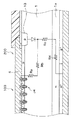
(第1実施形態)
本発明の第1実施形態について説明する。図1は、本実施形態にかかる半導体装置の断面図、図2は、図1に示す半導体装置の上面レイアウト図である。図1は、図2のA−A断面図に相当している。以下、これらの図を参照して、本実施形態の半導体装置について説明する。
(First embodiment)
A first embodiment of the present invention will be described. FIG. 1 is a cross-sectional view of the semiconductor device according to this embodiment, and FIG. 2 is a top layout view of the semiconductor device shown in FIG. FIG. 1 corresponds to the AA cross-sectional view of FIG. Hereinafter, the semiconductor device of this embodiment will be described with reference to these drawings.
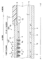
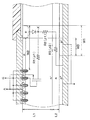
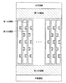
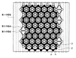
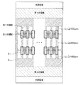
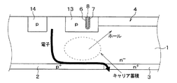
図1に示すように、本実施形態の半導体装置は、例えば不純物濃度が1×10¹³〜1×1014cm−3とされたn−型ドリフト層1を構成する半導体基板に対してIGBT100やFWD200を備えることにより構成されている。図1および図2に示したように、IGBT100が備えられるIGBT形成領域とFWD200が備えられるダイオード形成領域がセル領域とされ、セル領域の外周部に外周領域が備えられている。図2に示されるように、半導体装置を構成するチップの中央部がIGBT形成領域とされ、その周囲を囲むようにダイオード形成領域が配置されることでセル領域が構成され、さらにそのセル領域の外周を囲むように外周領域が配置されている。
As shown in FIG. 1, the semiconductor device according to the present embodiment includes, for example, an
セル領域におけるIGBT形成領域およびダイオード形成領域において、n−型ドリフト層1の裏面側における当該n−型ドリフト層1の表層部には、FS層1aが形成されている。このFS層1aは、n−型ドリフト層1よりも高不純物濃度のn型層にて構成され、空乏層の広がりを防ぐことで耐圧と定常損失の性能向上を図ると共に、基板裏面側から注入されるホールの注入量を制御するために備えてある。
In the IGBT formation region and the diode formation region in the cell region, the
また、セル領域におけるIGBT形成領域およびダイオード形成領域において、n−型ドリフト層1の裏面側におけるFS層1aの表層部には、コレクタ領域に相当するp+型不純物領域2およびカソード領域に相当するn+型不純物領域3が形成されている。p+型不純物領域2は、ボロン等のp型不純物が注入されて形成され、例えば不純物濃度が1×10¹⁷〜1×1020cm−3で構成されている。n+型不純物領域3は、リン等のn型不純物が注入されて形成され、例えば不純物濃度が1×10¹⁹〜1×1021cm−3で構成されている。n−型ドリフト層1の裏面側は基本的にはp+型不純物領域2とされているが、部分的にn+型不純物領域3が形成された構造とされている。
In the IGBT formation region and the diode formation region in the cell region, the surface layer portion of the
図2中の実線ハッチングを示した領域がn+型不純物領域3の形成されている領域であり、それ以外の領域がp+型不純物領域2の形成されている領域である。図2中の破線ハッチングを示した領域は、p型ディープウェル層13の形成されている領域である。
In FIG. 2, the region indicated by the solid line hatching is a region where the n + -
図2に示されるように、n−型ドリフト層1の裏面側は基本的にはp+型不純物領域2とされているが、部分的にn+型不純物領域3が形成された構造とされている。本実施形態の場合、n+型不純物領域3は、セル領域において短冊状のものが複数本ストライプ状に配置された構造とされている。なお、n+型不純物領域3のうち短冊状の部分のものは、図2中では5本のものを縦方向に2つに分割したものとして描いてあるが、実際にはそれ以上の多数本が形成されている。
As shown in FIG. 2, the back surface side of the n −
また、セル領域におけるIGBT形成領域においては、n−型ドリフト層1の表層部には、所定厚さのp型ベース領域4が形成されている。このp型ベース領域4を貫通してn−型ドリフト層1まで達するように複数個のトレンチ6が形成されており、このトレンチ6によってp型ベース領域4が複数個に分離されている。具体的には、トレンチ6は複数個所定のピッチ(間隔)で形成されており、図1の奥行き方向(紙面垂直方向)において各トレンチ6が平行に延設されたストライプ構造、もしくは並行に延設されたのちその先端部において引き回されることで環状構造とされている。そして、環状構造とされる場合、各トレンチ6が構成する環状構造は複数本ずつを1組として多重リング構造が構成され、隣接する多重リング構造同士の長手方向が平行となるように配置されている。
In the IGBT formation region in the cell region, a p-
隣接するトレンチ6によってp型ベース領域4が複数に分割された状態となるが、少なくともその一部は、チャネル領域を構成するチャネルp層4aとなり、このチャネルp層4aの表層部に、エミッタ領域に相当するn+型不純物領域5が形成されている。なお、本実施形態では、分割された各p型ベース領域4がチャネルp層4aとなる場合を図示してあるが、そのうちの一部にn+型不純物領域5を形成しないことで、IGBTとして機能する部分を間引いた構造(以下、間引き構造という)とされても良い。
The p-
n+型不純物領域5は、n−型ドリフト層1よりも高不純物濃度で構成され、p型ベース領域4内において終端しており、かつ、トレンチ6の側面に接するように配置されている。より詳しくは、トレンチ6の長手方向に沿って棒状に延設され、トレンチ6の先端よりも内側で終端した構造とされている。
The n + -
各トレンチ6内は、各トレンチ6の内壁表面を覆うように形成されたゲート絶縁膜7と、このゲート絶縁膜7の表面に形成されたドープトPoly−Si等により構成されるゲート電極8とにより埋め込まれている。ゲート電極8は、図1とは別断面において互いに電気的に接続され、同電位のゲート電圧が印加される様になっている。このような構造により、トレンチゲート構造が構成されている。
Each
さらに、n+型不純物領域5およびチャネルp層4aは、層間絶縁膜9に形成されたコンタクトホール9aを通じてエミッタ電極に相当する上部電極10と電気的に接続されており、上部電極10や図示しない配線などを保護するように保護膜11が形成されている。そして、p+型不純物領域2の裏面側に下部電極12が形成されることにより、IGBT100が構成されている。
Further, the n + -
一方、セル領域におけるダイオード形成領域でも、IGBT形成領域と同様に、n−型ドリフト層1の表層部に所定厚さのp型ベース領域4が形成されている。さらに、p型ベース領域4の周囲を囲むように、p型ベース領域4よりも接合深さが深くされたp型ディープウェル層13が形成されている。このp型ディープウェル層13は、p型ベース領域4よりも高不純物濃度で構成され、例えば不純物濃度が1×10¹⁸〜1×1019cm−3で構成されている。
On the other hand, also in the diode formation region in the cell region, the p-
このため、ダイオード形成領域に備えられたp型ベース領域4およびp型ディープウェル層13をアノードとし、n−型ドリフト層1およびn+型不純物領域3をカソードとしてPN接合されたダイオード構造を有するFWD200が構成されている。このFWD200は、p型ディープウェル層13に対して上部電極10がアノード電極として電気的に接続され、n+型不純物領域3に対して下部電極12がカソード電極として電気的に接続された構造とされている。
Therefore, the p-
このため、IGBT100とFWD200とは、エミッタとアノードとが電気的に接続されると共に、コレクタとカソードとが電気的に接続されることで、同一チップにおいて互いに並列接続された構造とされている。
Therefore, the
なお、外周領域においては、図示しないが、n−型ドリフト層1の表層部において、セル領域の外周を囲むようにp型ベース領域4よりも深くされたp型拡散層が形成され、更にp型拡散層の外周を囲むようにp型ガードリング層が多重リング構造として形成されるなど、外周耐圧構造が構成されている。この外周耐圧構造により、電界が偏り無く広げら得ることで、半導体装置の耐圧向上が図られている。
In the outer peripheral region, although not shown, a p-type diffusion layer deeper than the p-
以上のように、本実施形態にかかるIGBT100とFWD200とを一体化した半導体装置が構成されている。このように構成された半導体装置は、例えば直流−交流変換を行うためのインバータ回路などのスイッチング回路に備えられ、IGBT100がスイッチング素子として機能させられると共に、FWD200がIGBT100をオフしたときに還流電流を流す還流素子として機能させられる。
As described above, the semiconductor device in which the
このとき、FWD200では、ダイオード形成領域に備えられたp型ベース領域4およびp型ディープウェル層13がアノードとして機能することで、ダイオード動作を行う。ところが、深いp型ディープウェル層13がアノードとなるために、p型ディープウェル層13からのホール注入が多くなってFWD200の耐量を低下させる可能性がある。
At this time, in the
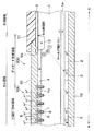
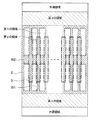
一方、図3に示す半導体装置の断面図に表されるように、p型ディープウェル層13からn+型不純物領域3までの距離が長いと、キャリアのライフタイムτの関係から、セル終端部、つまりp型ディープウェル層13のうちセル領域の外縁近傍からのホールが届かず、実質的にアノードとして機能する領域が減少する。このため、深いp型ディープウェル層13からのホール注入を抑制してFWD200の耐量を確保しつつ、実質的にアノードとして機能する領域を大きくできるように、各部の設計を行っている。以下、この設計について説明する。
On the other hand, as shown in the cross-sectional view of the semiconductor device shown in FIG. 3, if the distance from the p-type
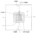
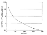
図4は、図1に示す半導体装置のダイオード作動を行うときの等価回路を模式的に描いた断面図である。また、図5は、図1に示す半導体装置のVAK−If特性を示した図である。アノード−カソード間電圧VAKは、FWD200の順方向電圧Vfと同等であるため、図5の特性は、FWD200のVf−If特性に相当する。
FIG. 4 is a cross-sectional view schematically showing an equivalent circuit when the diode operation of the semiconductor device shown in FIG. 1 is performed. FIG. 5 is a graph showing VAK-If characteristics of the semiconductor device shown in FIG. Since the anode-cathode voltage VAK is equivalent to the forward voltage Vf of the
まず、IGBT100とFWD200の等価回路は、図4中に示したものとなる。すなわち、IGBT100のコレクタに対してn−型ドリフト層1の横方向の内部抵抗R1(抵抗率ρ1)が接続されている。そして、IGBT100のエミッタ−コレクタ間と内部抵抗R1がFWD200に対して並列接続されていると共に、これらFWD200等に対してn−型ドリフト層1の縦方向の内部抵抗R2(抵抗率ρ1)と、FS層1aの横方向の内部抵抗R3(抵抗率ρ2)が直列接続されている。また、p型ディープウェル層13の外周側端部をn−型ドリフト層1の裏面側に投影した位置から、n+型不純物領域3とp+型不純物領域2との境界部までの距離をW1とし、FWD200として機能するp型ベース領域4の端部(p型ベース領域4のうちIGBT100とFWD200との境界部(最も外側のトレンチ5の側壁))からp型ディープウェル層13の外周側端部までの距離をW2とする。p型ディープウェル層13とp型ベース領域4との境界部を裏面側に投影した位置よりカソード領域となるn+型不純物領域3とコレクタ領域となるp+型不純物領域2との境界部までの距離をW3とする。また、n−型ドリフト層1の厚みをL1、FS層1aの厚みをL2とする。
First, an equivalent circuit of the
また、図5に示すVAK−If特性より、スナップバック電圧が最も大きくなるときのアノード−カソード間電圧VAKをVAK1とし、FWD200がダイオード動作し始めるときのアノード−カソード間電圧VAKをVAK2とする。また、VAK−If特性が線形となるところから直線を引いたときの切片がp型ディープウェル層13とn−型ドリフト層1との間のビルトインポテンシャル、つまり理論上ダイオード動作するのに必要な電圧であり、このビルトインポテンシャルをVAK(th)とする。
Further, from the VAK-If characteristic shown in FIG. 5, the anode-cathode voltage VAK when the snapback voltage becomes the highest is VAK1, and the anode-cathode voltage VAK when the
これらに基づき、以下の関係式が成り立つ。まず、数式1に示すように、スナップバック電圧VSBは、VAK1とVAK2の差として表される。
Based on these, the following relational expression holds. First, as shown in
(数1) VSB=VAK1−VAK2
また、スナップバック電圧VSBが最も大きくなる時のVAK1は、FWD200がダイオード動作を行っていることが必要であることから、図4中の点Xの電位に基づいて、次式を導くことができる。なお、下記の式で、Iは、IGBT100からn−型ドリフト層1の内部抵抗R1、R2およびFS層1aの内部抵抗R3を通って流れる電流を意味している。また、下記の式では、IGBT100のチャネル抵抗に関しては、非常に小さいことから無視している。
(Expression 1) VSB = VAK1-VAK2
Further, VAK1 when the snapback voltage VSB becomes the largest needs to be that the
(数2) Vth=I・R1
(数3) I=VAK1・(R1/(R1+R2+R3))
(数4) VAK1=VAK(th)×((R1+R2+R3)/R1)
また、p型ディープウェル層13とn−型ドリフト層1との間のビルトインポテンシャルVAK(th)は、FWD200がダイオード動作し始めた電圧VAK2とほぼ等しいため、次式で表せる。
(Expression 2) Vth = I · R1
(Expression 3) I = VAK1 · (R1 / (R1 + R2 + R3))
(Expression 4) VAK1 = VAK (th) × ((R1 + R2 + R3) / R1)
Further, the built-in potential VAK (th) between the p-type
(数5) VAK2≒VAK(th)
この数式5および上記した数式4を上記数式1に代入すると、次式を導出することができる。
(Expression 5) VAK2≈VAK (th)
By substituting
(数6) VSB≒((R2+R3)/R1)×VAK(th)
そして、R1〜R3は、それぞれR1=W2・ρ1/L1、R2=ρ1・L1/W2、R3=W1・ρ2/L2で表されることから、数式6を次式に変換できる。
(Expression 6) VSB≈ ((R2 + R3) / R1) × VAK (th)
Since R1 to R3 are represented by R1 = W2 · ρ1 / L1, R2 = ρ1 · L1 / W2, and R3 = W1 · ρ2 / L2, respectively,
(数7)
VSB≒((L1・ρ1/W2+W1・ρ2/L2)/(W2・ρ1/L1))×VAK(th)
ここで、VSB/VAK(th)に対してIGBT100およびFWD200の形状や濃度等、IGBT100およびFWD200の構造に基づいて決まる第1パラメータをk1とし、ビルトインポテンシャルVAK(th)に対するスナップバック電圧VSBの比であるVSB/VAK(th)に対して第1パラメータを掛けた値(=k1・VSB/VAK(th))をKとする。また、ビルトインポテンシャルを表すVAK(th)は定数であり、スナップバック電圧VSBが小さいほど非線形性が小さくなって線形性が改善されることから、Kが小さくなるほど線形性を改善できる。したがって、次式で表される右辺がそのK以下となるようにすることで、線形性の改善を図ることができる。
(Equation 7)
VSB≈ ((L1 · ρ1 / W2 + W1 · ρ2 / L2) / (W2 · ρ1 / L1)) × VAK (th)
Here, the first parameter determined based on the structure of the
(数8) K≧((L1・ρ1/W2+W1・ρ2/L2)/(W2・ρ1/L1))
また、p型ディープウェル層13の外周端部がゲートのバイアスによって影響を受けないダイオードとして動作させるためのW2の条件は、上記数式8に基づいて下記数式9および数式10のように求めることができる。なお、n−型ドリフト層1の抵抗率ρ1に対してFS層1aの抵抗率ρ2は十分に小さいことから、W1・ρ2/L2≒0と見なしている。
(Equation 8) K ≧ ((
Further, the condition of W2 for operating the outer peripheral end portion of the p-type
(数9) K≧((L1・ρ1/W2)/(W2・ρ1/L1))=L12/W22
(数10) W2≧L1/K1/2
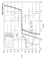
また外周端部におけるスナップバック電圧を−40℃におけるVAK(th)=0.8[V]に対して無視できる0.1V以下にする場合は、実験結果を示した図8よりK≧2.5となる。すなわち、図8中に示しように、L1=135μmとした場合には、W2=85μmのときにスナップバック電圧が0.1Vとなることから、数式9にL1=135μm、W2=85μmを代入すると、K≧2.5となる。同様に、L1=80μmとした場合には、W2=50μmのときにスナップバック電圧が0.1Vとなることから、数式9にL1=80μm、W2=50μmを代入すると、K≧2.56となる。このように、いずれの結果からもK≧2.5を満たすようにすることで、スナップバック電圧を0.1V以下に抑えることが可能となることが判る。なお、図8に示すSim解析では、W1=0μm、L2>0、W3は任意の値に設定している。
(Equation 9) K ≧ ((L1 · ρ1 / W2) / (W2 · ρ1 / L1)) = L1 2 / W2 2
(Formula 10) W2 ≧ L1 / K 1/2
Further, when the snapback voltage at the outer peripheral end is set to 0.1 V or less that can be ignored with respect to VAK (th) = 0.8 [V] at −40 ° C., K ≧ 2. 5 That is, as shown in FIG. 8, when L1 = 135 μm, the snapback voltage becomes 0.1 V when W2 = 85 μm. Therefore, when L1 = 135 μm and W2 = 85 μm are substituted into
またW2が数式10を満たしている場合であっても、W1が大きい場合やライフタイムが短い場合は、ディープウェル層13の外周端部から注入されたホールがカソードとなるn+型不純物領域3まで届かなくなるため、実効的なW2が短く(R1が小さく)なりスナップバックが出現する。このため、ライフタイムを例えば2μsとした場合において、W1、W2とスナップバック電圧VSBとの関係について調べた。そのSim結果を図9に示す。また、図10は、本実施形態にかかる半導体装置のVce−If特性について電子線照射量を60kGyとして測定した結果を示した図である。この図においてVceが部分的にマイナス方向に突出したものがスナップバック電圧VSBであり、この図のスナップバック電圧VSBを取り出してプロットしたのが図9に相当する。
Even if W2 satisfies
スナップバック電圧VSBが−40℃のVak(th)0.8Vに対して無視できる0.1V以下に抑制できるようにするためには、図9より、次式が成り立つ。なお、図9に示す実験では、L1=125μm、W2=85μmL2=1μm、W3は任意の値としている。
(数11) W2−W1≧10μm
一方、距離W3については、図3に示すように、ホールがp型ディープウェル層13から斜め方向に最短距離でp+型不純物領域2とn+型不純物領域3との境界位置に向かってホールが注入された時、注入量が大きくなり破壊しないためには、拡散長よりも上で述べた最短距離が十分大きいことが必要となることから、図4および三角形の関係で示される三平方の定理より、数式12が成り立つ。そして、これを変換すると数式13を導出できる。なお、Dは、n-型ドリフト層1内でのキャリアの拡散係数であり、k2は、p型ディープウェル層13の深さ、濃度、耐量等のp型ディープウェル層13の構造に基づいて決まる第2パラメータである。
In order to suppress the snapback voltage VSB to 0.1 V or less which can be ignored with respect to Vak (th) 0.8 V of −40 ° C., the following equation is established from FIG. In the experiment shown in FIG. 9, L1 = 125 μm, W2 = 85 μmL2 = 1 μm, and W3 are arbitrary values.
(Equation 11) W2-W1 ≧ 10 μm
On the other hand, with respect to the distance W3, as shown in FIG. 3, the holes are formed toward the boundary position between the p + -
(数12) W32+L12≧(k2・(Dτ) 1/2 ) 2
(数13) W3≧((k2・(Dτ)1/2)2−L12)^(1/2)
そして、距離W1〜W3については、半導体装置の小型化などを考慮すると、上記数式を満たす中で最も小さい値であることが好ましいため、またW1−W3は耐圧の観点から大きな値となることが望ましいため次式が成り立つ関係とするのが良い。
(Expression 12) W3 2 + L1 2 ≧ ( k2 · ( Dτ ) 1/2 ) 2
(Formula 13) W3 ≧ ((k2 · (Dτ) 1/2 ) 2 −L1 2 ) ^ (1/2)
The distances W1 to W3 are preferably the smallest value satisfying the above mathematical formula in consideration of miniaturization of the semiconductor device, and W1 to W3 may be a large value from the viewpoint of breakdown voltage. Since it is desirable, it is preferable to have a relationship that satisfies the following equation.
(数14)
W2=L1/K1/2
かつ
W2−W1=10μm
かつ
W3=((k2・(Dτ)1/2)2−L12)^(1/2)
よって、本実施形態の半導体装置では、距離W1、W2、W3が数式14を満たす値に設定している。
(Equation 14)
W2 = L1 / K 1/2
And W2-W1 = 10μm
And W3 = ((
Therefore, in the semiconductor device of this embodiment, the distances W1, W2, and W3 are set to values that satisfy
以上説明したように、本実施形態の半導体装置では、IGBT100とFWD200を備えた構造において、ダイオード形成領域に備えられたp型ベース領域4およびp型ディープウェル層13をアノードとして機能させることで、ダイオード動作を行わせている。
As described above, in the semiconductor device according to the present embodiment, in the structure including the
そして、p型ディープウェル層13の外周側端部をn−型ドリフト層1の裏面側に投影した位置より、n+型不純物領域3とp+型不純物領域2との境界部までの距離W1とFWD200として機能するp型ベース領域4の端部からp型ディープウェル層13の外周側端部までの距離W3が数式14を満たす値となるようにしている。
The distance W1 from the position where the outer peripheral side end of the p-type
これにより、深いp型ディープウェル層13がアノードとなるときに、p型ディープウェル層13からのホール注入が多くなることでFWD200の耐量が低下してしまうことを抑制しつつ、p型ディープウェル層13のうちセル領域の外縁近傍からのホールが届かせ、実質的にアノードとして機能する領域が減少することを抑制することができる。
Thus, when the deep p-type
(第2実施形態)
本発明の第2実施形態について説明する。本実施形態は、第1実施形態に対して異なる場所でもFWDのVf−If特性の線形性を改善できる構成を採用したものであり、その他に関しては第1実施形態と同様であるため、第1実施形態と異なる部分についてのみ説明する。
(Second Embodiment)
A second embodiment of the present invention will be described. The present embodiment employs a configuration that can improve the linearity of the Vf-If characteristic of the FWD even at different locations with respect to the first embodiment, and is otherwise the same as the first embodiment. Only portions different from the embodiment will be described.
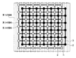
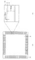
図11(a)は、本実施形態にかかる半導体装置の上面レイアウト図であり、図11(b)は、図11(a)の領域Rの部分拡大図である。なお、図11(a)、(b)は断面図ではないが、図を見易くするために部分的にハッチングを示してある。また、図12(a)〜(c)は、それぞれ、図11(b)に示すA−A’、B−B’、C−C’断面図である。ただし、図12(c)については、より各領域の断面構造が明確になるように、図11(b)のC−C’断面を更に延長して多くのセル分備えた図としてある。なお、本実施形態の半導体装置では、p型チャネル領域4aの表層部にコンタクト領域4bを形成した構造としてあり、このコンタクト領域4bを介して上部電極10と電気的に接続されるようにしてあるが、基本的な構造は第1実施形態と同様である。
FIG. 11A is a top surface layout diagram of the semiconductor device according to the present embodiment, and FIG. 11B is a partially enlarged view of a region R in FIG. 11A and 11B are not cross-sectional views, but are partially hatched to make the drawing easier to see. 12A to 12C are cross-sectional views taken along lines A-A ', B-B', and C-C 'shown in FIG. 11B, respectively. However, FIG. 12C is a diagram in which the C-C ′ cross section of FIG. 11B is further extended and provided for many cells so that the cross-sectional structure of each region becomes clearer. Note that the semiconductor device of this embodiment has a structure in which the
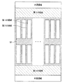
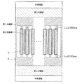
図11(a)、(b)に示すように、本実施形態の半導体装置は、外周領域内に第1〜第3の領域を備えた構成とされている。具体的には、トレンチ6の側面においてエミッタ領域に相当するn+型不純物領域5が形成されていてIGBT100として機能する部分が含まれる領域を第1の領域、この第1の領域に併設されたエミッタ領域に相当するn+型不純物領域5が形成されておらずFWD200として機能させる部分が含まれる領域を第2の領域、トレンチゲート構造の長手方向の先端位置においてp+型不純物領域2が形成されている領域のうちp型ガードリング層14などが形成された外周領域よりも内側(つまりセル領域の外縁部におけるFWD200が形成されている領域)を第3の領域としている。
As shown in FIGS. 11A and 11B, the semiconductor device of this embodiment is configured to include first to third regions in the outer peripheral region. Specifically, an n + -
このようなゲート電極8の先端位置においても、FWD200のVf−If特性の線形性の問題が発生する。このため、第3の領域に備えられるp型ベース領域4とp型ディープウェル層13とによって構成されるFWD200について、第1実施形態と同様に、各種寸法について規定している。
Even at the tip position of the
具体的には、本実施形態でも、図12(a)、(b)中に示したように、p型ディープウェル層13の外周側端部をn−型ドリフト層1の裏面側に投影した位置から、n+型不純物領域3とp+型不純物領域2との境界部までの距離をW1とし、FWD200として機能するp型ベース領域4の端部(p型ベース領域4のうちIGBT100とFWD200との境界部(エミッタ領域に相当するn+型不純物領域5の先端位置))からp型ディープウェル層13の外周側端部までの距離をW2とする。p型ディープウェル層13とp型ベース領域4との境界部を裏面側に投影した位置よりカソード領域となるn+型不純物領域3とコレクタ領域となるp+型不純物領域2との境界部までの距離をW3とする。また、n−型ドリフト層1の厚みをL1とする。
Specifically, also in this embodiment, as shown in FIGS. 12A and 12B, the outer peripheral side end of the p-type
このように構成された半導体装置におけるトレンチゲート構造の先端位置においても、p型ベース領域4とp型ディープウェル層13を長くして内部抵抗を大きくしたいが、これらが長くなり過ぎるとp型ディープウェル層13のうちのセル領域の終端からn+型不純物領域3までホールが届かなくなる。このため、W1〜W3が上記第1実施形態で示した数式10、11、13、好ましくは数式14の関係を満たすようにすることで、FWD200のVf−If特性の線形性を改善することが可能となる。
Even at the tip position of the trench gate structure in the semiconductor device configured as described above, it is desired to increase the internal resistance by increasing the p-
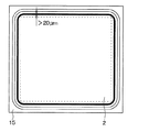
また、図12(c)に示すように、第1、第2の領域において、エミッタ領域に相当するn+型不純物領域5を形成しない間引き構造としている。このような間引き構造とすることで、その間引き部分にてダイオード動作させ、隣り合うトレンチゲート構造の間にFWD200が構成されるようにしている。
Further, as shown in FIG. 12C, a thinning structure is employed in which the n +
この間引き構造のうち、第2の領域に構成される部分の少なくとも一部について、n+型不純物領域5が形成されておらずp型ベース領域4のみが形成されている箇所の最も端から端のトレンチゲート構造の間の距離を第2の領域でのFWD200の幅W4とすると、W4≧20μmとなるようにしている。図13は、第2の領域でのFWD200の幅W4とFWD200がオンし始める電圧VF(スナップバック電圧VSBに相当)との関係を示したグラフである。この図に示されるように、第2の領域でのFWD200の幅W4が20μmを超えるとFWD200がオンし始める電圧VFが急に上昇し始める。この結果に基づき、第2の領域でのFWD200の幅W4が20μm以上となるようにしている。これにより、FWD200のオン電圧を低減することが可能になる。ただしFWDのリカバリー(SW)損失を低減することを目的にSW動作の直前又は動作中にゲートに電圧を印加するような制御を行う場合、このW4<20μmした方がSW損失を低減できる場合もある。この場合もW1〜W3を本特許の条件を満たすことによりFWDの線形性の向上やスナップバックによるVfの急激な上昇を抑制することができる。
In this thinning structure, at least a part of the portion formed in the second region is from the end to the end where only the p-
以上説明したように、トレンチゲート構造の先端位置においても、W1〜W3が上記第1実施形態で示した数式10、11、13、好ましくは数式14の関係を満たすようにすることで、FWD200のVf−If特性の線形性を改善することが可能となる。またこの構成で第3の領域と第2の領域の距離を縮めることにより第3の領域がONすることにより上がった電流密度を第2の領域に効率的に伝えられるため線形性がより向上される。さらに、第2の領域でのFWD200の幅W4が20μm以上となるようにすることで、FWD200のオン電圧を低減することが可能になる。
As described above, even at the front end position of the trench gate structure, W1 to W3 satisfy
(第3実施形態)
本発明の第3実施形態について説明する。本実施形態は、第2実施形態に対して異なる場所でもFWDのVf−If特性の線形性を改善しつつ、IGBTのオン損失を低減できる構成を採用したものであり、その他に関しては第2実施形態と同様であるため、第2実施形態と異なる部分についてのみ説明する。
(Third embodiment)
A third embodiment of the present invention will be described. The present embodiment employs a configuration that can reduce the on-loss of the IGBT while improving the linearity of the VWD-If characteristics of the FWD even at different locations with respect to the second embodiment. Since it is the same as the embodiment, only the parts different from the second embodiment will be described.
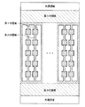
図14は、本実施形態にかかる半導体装置の上面レイアウト図である。なお、図14は断面図ではないが、図を見易くするために部分的にハッチングを示してある。この図に示すように、第1の領域を長手方向において2つに分割、つまりエミッタ領域に相当するn+型不純物領域5を長手方向方向において2つに分割しており、分割した第1の領域の間においてn+型不純物領域5が形成されておらず、隣接するトレンチゲート構造の間の領域にp型ベース領域4のみが形成されることでFWD200が形成されるようにしている。
FIG. 14 is a top surface layout diagram of the semiconductor device according to the present embodiment. Although FIG. 14 is not a cross-sectional view, hatching is partially shown for easy understanding of the drawing. As shown in this figure, the first region is divided into two in the longitudinal direction, that is, the n + -
このように、第1の領域を長手方向において2つに分割し、分割した第1の領域の間においてFWD200が構成されるようにしても良い。このようにすれば、エミッタ領域に相当するn+型不純物領域5の近くにダイオード動作する第2の領域を形成できる。これによりFWD200の面積が増えることやこの領域が第3の領域の補助的な役割することでより効率的にFWD200の電流密度を向上できることで半導体装置全体のスナップバック電圧を低減することが可能になる。
In this way, the first region may be divided into two in the longitudinal direction, and the
なお、このように第1の領域を長手方向において分割する場合、その第1の領域の間の幅Wを数式10のW2の2倍以上に取ることにより、この領域をトレンチゲート構造の両先端位置に配置される第3の領域の代わりとすることもできる。また、ここでは第1の領域を長手方向において2つに分割する場合について説明したが、複数、つまり2つに限らず3つ以上の数に分割しても構わない。
When the first region is divided in the longitudinal direction in this way, the width W between the first regions is set to be equal to or more than twice W2 in
(第4実施形態)
本発明の第4実施形態について説明する。本実施形態は、第2実施形態に対して第1の領域と第2の領域のレイアウトを変更したものであり、その他に関しては第2実施形態と同様であるため、第2実施形態と異なる部分についてのみ説明する。
(Fourth embodiment)
A fourth embodiment of the present invention will be described. This embodiment is different from the second embodiment in the layout of the first region and the second region, and is otherwise the same as that of the second embodiment, and is different from the second embodiment. Only will be described.
図15は、本実施形態にかかる半導体装置の上面レイアウト図である。なお、図14は断面図ではないが、図を見易くするために部分的にハッチングを示してある。この図に示すように、複数本並べられた第1の領域の一部、具体的には隣り合う第1の領域の対向する辺の一部を凹ませた図中破線で囲んだ部分をエミッタ領域に相当するn+型不純物領域5が備えられていない領域とし、本実施形態では、この領域を第2の領域とした構成としている。つまり、本実施形態では、上記第2実施形態のように各第1の領域や各第2の領域がそれぞれ同じ幅で構成されているのではなく、第1の領域の間において部分的に第2の領域の幅を広げた構造にしている。
FIG. 15 is a top surface layout diagram of the semiconductor device according to the present embodiment. Although FIG. 14 is not a cross-sectional view, hatching is partially shown for easy understanding of the drawing. As shown in this figure, a portion surrounded by a broken line in the figure in which a part of a plurality of first regions arranged in parallel, specifically a part of the opposite side of the adjacent first region is recessed, is an emitter. The region is not provided with the n + -
このように、一部の第2の領域の幅W4を広げることにより、第2の領域に構成されるFWD200がダイオード動作し易くなる。これにより、FWD200の面積が増えることやこの領域が第3の領域の補助的な役割することでより効率的にFWD200の電流密度を向上できることで半導体装置全体のスナップバック電圧を小さくすることが可能になる。
Thus, by increasing the width W4 of a part of the second region, the
(第5実施形態)
本発明の第5実施形態について説明する。本実施形態も、第2実施形態に対して第1の領域と第2の領域のレイアウトを変更したものであり、その他に関しては第2実施形態と同様であるため、第2実施形態と異なる部分についてのみ説明する。
(Fifth embodiment)
A fifth embodiment of the present invention will be described. This embodiment is also the same as the second embodiment except that the layout of the first region and the second region is changed with respect to the second embodiment. Only will be described.
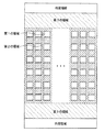
図16は、本実施形態にかかる半導体装置の上面レイアウト図である。なお、図16は断面図ではないが、図を見易くするために部分的にハッチングを示してある。この図に示すように、第1の領域を紙面上下方向、つまりトレンチゲート構造の長手方向において複数個に分割し、分割した第1の領域の間に第1の領域とほぼ同寸法の第2の領域が配置されるようにすることで各第1の領域がマトリクス状に配置された構造にしている。つまり、トレンチゲート構造の長手方向に並べぶ第1の領域を1つの列として、第1の領域の列が複数列並べて配置され、隣り合う各列の第1の領域が対向配置される構造とされている。このような構造としても、分割された各第1の領域の間の第2の領域に構成されるFWD200がダイオード動作し易くなる。これにより、FWD200の面積が増えることやこの領域が第3の領域の補助的な役割することでより効率的にFWD200の電流密度を向上できることで半導体装置全体のスナップバック電圧を小さくすることが可能になる。
FIG. 16 is a top surface layout diagram of the semiconductor device according to the present embodiment. Although FIG. 16 is not a cross-sectional view, hatching is partially shown for easy understanding of the drawing. As shown in this figure, the first region is divided into a plurality of portions in the vertical direction of the page, that is, in the longitudinal direction of the trench gate structure, and a second region having substantially the same size as the first region is provided between the divided first regions. Thus, each of the first regions is arranged in a matrix. That is, a structure in which the first region arranged in the longitudinal direction of the trench gate structure is one column, a plurality of columns of the first region are arranged side by side, and the first region of each adjacent column is opposed to each other. Has been. Even with such a structure, the
(第6実施形態)
本発明の第6実施形態について説明する。本実施形態は、第5実施形態に対して第1の領域と第2の領域のレイアウトを変更したものであり、その他に関しては第5実施形態と同様であるため、第5実施形態と異なる部分についてのみ説明する。
(Sixth embodiment)
A sixth embodiment of the present invention will be described. In the present embodiment, the layout of the first region and the second region is changed with respect to the fifth embodiment, and the other parts are the same as those in the fifth embodiment, and therefore different from the fifth embodiment. Only will be described.
図17は、本実施形態にかかる半導体装置の上面レイアウト図である。なお、図17は断面図ではないが、図を見易くするために部分的にハッチングを示してある。この図に示すように、本実施形態でも、第1の領域を紙面上下方向、つまりトレンチゲート構造の長手方向において複数個に分割し、分割した第1の領域の間に第1の領域とほぼ同寸法の第2の領域が配置されるようにしているが、トレンチゲート構造の長手方向に並べぶ第1の領域を1つの列として、第1の領域の列が複数列並べて配置されているものの、隣り合う各列の第1の領域が互いにずれて配置される構造とされている。つまり、各第1の領域が千鳥状に配置された構造とされている。このような構造としても、分割された各第1の領域の間の第2の領域に構成されるFWD200がダイオード動作し易くなる。これにより、FWD200の面積が増えることやこの領域が第3の領域の補助的な役割することでより効率的にFWD200の電流密度を向上できることで半導体装置全体のスナップバック電圧を小さくすることが可能になる。
FIG. 17 is a top surface layout diagram of the semiconductor device according to the present embodiment. Although FIG. 17 is not a cross-sectional view, hatching is partially shown for easy understanding of the drawing. As shown in this figure, also in this embodiment, the first region is divided into a plurality of portions in the vertical direction of the page, that is, in the longitudinal direction of the trench gate structure, and the first region is substantially the same as the first region between the divided first regions. The second region of the same size is arranged, but the first region arranged in the longitudinal direction of the trench gate structure is regarded as one column, and a plurality of columns of the first region are arranged. However, the first regions in the adjacent columns are arranged so as to be shifted from each other. That is, each first region has a staggered structure. Even with such a structure, the
(第7実施形態)
本発明の第7実施形態について説明する。本実施形態は、第6実施形態に対して第1の領域と第2の領域のレイアウトを変更したものであり、その他に関しては第6実施形態と同様であるため、第6実施形態と異なる部分についてのみ説明する。
(Seventh embodiment)
A seventh embodiment of the present invention will be described. In the present embodiment, the layout of the first region and the second region is changed with respect to the sixth embodiment, and the other parts are the same as those in the sixth embodiment, and therefore different from the sixth embodiment. Only will be described.
図18は、本実施形態にかかる半導体装置の上面レイアウト図である。なお、図18は断面図ではないが、図を見易くするために部分的にハッチングを示してある。この図に示すように、本実施形態でも、第1の領域を紙面上下方向、つまりトレンチゲート構造の長手方向において複数個に分割しているが、第6実施形態と比べて分割場所の間隔を長くした構造としている。このような構造としても、分割された各第1の領域の間の第2の領域に構成されるFWD200がダイオード動作し易くなる。これにより、FWD200の面積が増えることやこの領域が第3の領域の補助的な役割することでより効率的にFWD200の電流密度を向上できることで半導体装置全体のスナップバック電圧を小さくすることが可能になる。
FIG. 18 is a top surface layout diagram of the semiconductor device according to the present embodiment. Although FIG. 18 is not a cross-sectional view, hatching is partially shown for easy understanding of the drawing. As shown in this figure, also in this embodiment, the first region is divided into a plurality of parts in the vertical direction of the page, that is, in the longitudinal direction of the trench gate structure. It has a long structure. Even with such a structure, the
(第8実施形態)
本発明の第8実施形態について説明する。本実施形態は、第4実施形態に対して第1の領域と第2の領域のレイアウトを変更したものであり、その他に関しては第4実施形態と同様であるため、第4実施形態と異なる部分についてのみ説明する。
(Eighth embodiment)
An eighth embodiment of the present invention will be described. This embodiment is different from the fourth embodiment in the layout of the first region and the second region, and is otherwise the same as the fourth embodiment. Only will be described.
図19は、本実施形態にかかる半導体装置の上面レイアウト図である。なお、図19は断面図ではないが、図を見易くするために部分的にハッチングを示してある。この図に示すように、本実施形態でも、隣り合う第1の領域の対向する辺の一部を凹ませて第2の領域としているが、第4実施形態のように隣り合う第1の領域の対向する辺の同じ場所に第2の領域を配置するのではなく、互い違いに第2の領域を配置した構造としている。このような構造としても、第2の領域に構成されるFWD200がダイオード動作し易くなり、FWD200の面積が増えることやこの領域が第3の領域の補助的な役割することでより効率的にFWD200の電流密度を向上できることで半導体装置全体のスナップバック電圧を小さくすることが可能になる。
FIG. 19 is a top surface layout diagram of the semiconductor device according to the present embodiment. Although FIG. 19 is not a cross-sectional view, hatching is partially shown for easy understanding of the drawing. As shown in this figure, also in this embodiment, a part of the opposite side of the adjacent first region is recessed to form the second region, but the adjacent first region as in the fourth embodiment. Instead of arranging the second regions at the same place on the opposite sides of the two, the second regions are arranged alternately. Even in such a structure, the
(第9実施形態)
本発明の第9実施形態について説明する。本実施形態は、第2実施形態に対して第1〜第3の領域のレイアウトを変更したものであり、その他に関しては第2実施形態と同様であるため、第2実施形態と異なる部分についてのみ説明する。
(Ninth embodiment)
A ninth embodiment of the present invention will be described. In the present embodiment, the layout of the first to third regions is changed with respect to the second embodiment, and the other aspects are the same as those of the second embodiment. Therefore, only the portions different from the second embodiment are described. explain.
図20は、本実施形態にかかる半導体装置の上面レイアウト図である。なお、図20は断面図ではないが、図を見易くするために部分的にハッチングを示してある。この図に示すように、本実施形態では、第3の領域をセル領域の外縁部に配置するのではなく、セル領域の中央位置に点在させるように配置し、かつ、第2の領域が第3の領域の間を繋ぐように配置された構造となるようにしている。 FIG. 20 is a top surface layout diagram of the semiconductor device according to the present embodiment. Although FIG. 20 is not a cross-sectional view, hatching is partially shown for easy understanding of the drawing. As shown in this figure, in the present embodiment, the third region is not disposed at the outer edge portion of the cell region, but is disposed so as to be scattered at the center position of the cell region, and the second region is The structure is arranged so as to connect the third regions.
具体的には、円形状に囲まれた範囲を第3の領域として、第3の領域が正六角形の各角部に配置された形状、つまりハニカム状に配置されたレイアウトとされ、各第3の領域を繋ぐ六角形の各辺に相当する位置に第2の領域が配置されたレイアウトとされている。図中破線はトレンチゲート構造を示しているが、紙面上下方向を長手方向として複数本のトレンチゲート構造が配置されており、その複数本のトレンチゲート構造が交差するように第1〜第3の領域がレイアウトされることになる。このトレンチゲート構造のトレンチ6の側面のうち第1の領域と接している場所にはエミッタ領域に相当するn+型不純物領域5が備えられ、第2の領域や第3の領域と接している場所にはエミッタ領域に相当するn+型不純物領域5が備えられていない構造となるようにしている。
Specifically, a range surrounded by a circular shape is defined as a third region, and the third region has a shape arranged at each corner of a regular hexagon, that is, a layout arranged in a honeycomb shape. The second area is arranged at a position corresponding to each side of the hexagon connecting the areas. The broken line in the figure shows the trench gate structure, but a plurality of trench gate structures are arranged with the vertical direction in the drawing as the longitudinal direction, and the first to third so that the plurality of trench gate structures cross each other. The area will be laid out. An n + -
このように、第1〜第3の領域のレイアウトを変更しても、第2実施形態と同様の効果を得ることができる。また第3の領域同士の距離が短くなるため効率よく第2の領域の電流密度を向上でき、これにより半導体装置全体のスナップバック電圧をより小さくすることが可能になる。 Thus, even if the layout of the first to third regions is changed, the same effect as that of the second embodiment can be obtained. In addition, since the distance between the third regions is shortened, the current density in the second region can be improved efficiently, thereby making it possible to further reduce the snapback voltage of the entire semiconductor device.
(第10実施形態)
本発明の第10実施形態について説明する。本実施形態は、第9実施形態に対して第1〜第3の領域のレイアウトを変更したものであり、その他に関しては第9実施形態と同様であるため、第9実施形態と異なる部分についてのみ説明する。
(10th Embodiment)
A tenth embodiment of the present invention will be described. In the present embodiment, the layout of the first to third regions is changed with respect to the ninth embodiment, and the other aspects are the same as those in the ninth embodiment. Therefore, only the portions different from the ninth embodiment are described. explain.
図21は、本実施形態にかかる半導体装置の上面レイアウト図である。なお、図21は断面図ではないが、図を見易くするために部分的にハッチングを示してある。この図に示すように、本実施形態でも、セル領域の外縁部に配置するのではなく、セル領域の中央位置に点在させるように配置し、かつ、第2の領域が第3の領域の間を繋ぐように配置された構造となるようにしている。そして、円形状に囲まれた範囲を第3の領域として、第3の領域が正方形の各角部に配置された形状、つまりマトリクス状に配置されたレイアウトとされ、各第3の領域を繋ぐ正方形の各辺に相当する位置に第2の領域が配置されたレイアウトとされている。 FIG. 21 is a top surface layout diagram of the semiconductor device according to the present embodiment. Although FIG. 21 is not a cross-sectional view, hatching is partially shown for easy understanding of the drawing. As shown in this figure, also in this embodiment, it is not arranged at the outer edge of the cell region, but is arranged so as to be scattered at the center position of the cell region, and the second region is the third region. The structure is arranged so as to connect each other. Then, the range surrounded by the circular shape is defined as a third region, and the third region is formed in a shape arranged in each corner of the square, that is, a layout arranged in a matrix, and connects the third regions. The layout is such that the second region is arranged at a position corresponding to each side of the square.
このように、第1〜第3の領域のレイアウトを変更しても、第9実施形態と同様の効果を得ることができる。 Thus, even if the layout of the first to third regions is changed, the same effect as in the ninth embodiment can be obtained.
(第11実施形態)
本発明の第11実施形態について説明する。本実施形態も、第9実施形態に対して第1〜第3の領域のレイアウトを変更したものであり、その他に関しては第9実施形態と同様であるため、第9実施形態と異なる部分についてのみ説明する。
(Eleventh embodiment)
An eleventh embodiment of the present invention will be described. This embodiment is also a modification of the layout of the first to third regions with respect to the ninth embodiment. Since the other aspects are the same as those of the ninth embodiment, only the parts different from the ninth embodiment are described. explain.
図22は、本実施形態にかかる半導体装置の上面レイアウト図である。なお、図22は断面図ではないが、図を見易くするために部分的にハッチングを示してある。この図に示すように、本実施形態でも、セル領域の外縁部に配置するのではなく、セル領域の中央位置に点在させるように配置し、かつ、第2の領域が第3の領域の間を繋ぐように配置された構造となるようにしている。そして、円形状に囲まれる範囲を第3の領域として、第3の領域が正三角形の各角部に配置されたレイアウトとされ、各第3の領域を繋ぐ正三角形の各辺に相当する位置に第2の領域が配置されたレイアウトとされている。 FIG. 22 is a top surface layout diagram of the semiconductor device according to the present embodiment. Although FIG. 22 is not a cross-sectional view, hatching is partially shown for easy understanding of the drawing. As shown in this figure, also in this embodiment, it is not arranged at the outer edge of the cell region, but is arranged so as to be scattered at the center position of the cell region, and the second region is the third region. The structure is arranged so as to connect each other. Then, a range surrounded by a circular shape is defined as a third region, the third region is arranged at each corner of the equilateral triangle, and the position corresponding to each side of the equilateral triangle connecting the third regions. The second area is arranged in the layout.
このように、第1〜第3の領域のレイアウトを変更しても、第9実施形態と同様の効果を得ることができる。 Thus, even if the layout of the first to third regions is changed, the same effect as in the ninth embodiment can be obtained.
(第12実施形態)
本発明の第12実施形態について説明する。本実施形態は、第2実施形態に対して半導体装置の基板裏面側のレイアウトについても考慮したものであり、その他に関しては第2実施形態と同様であるため、第2実施形態と異なる部分についてのみ説明する。
(Twelfth embodiment)
A twelfth embodiment of the present invention will be described. In the present embodiment, the layout on the back side of the substrate of the semiconductor device is also considered with respect to the second embodiment, and the other aspects are the same as those in the second embodiment. Therefore, only the differences from the second embodiment are described. explain.
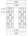
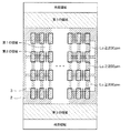
図23は、本実施形態にかかる半導体装置の上面レイアウト図である。なお、図23は断面図ではないが、図を見易くするために部分的にハッチングを示してある。この図に示すように、本実施形態では、第2実施形態のような第1〜第3の領域を備えた構造について、第1の領域の長手方向先端部よりもカソード領域に相当するn+型不純物領域3(図中一点鎖線で囲んだ領域)が図中矢印A1のように突き出すように形成されている。このような構造の場合、IGBT100におけるスナップバック電圧VSBが大きくなることが懸念されることから、本実施形態では、n+型不純物領域3を長手方向において図中矢印A2のように分割し、分割したn+型不純物領域3の間にコレクタ領域に相当するp+型不純物領域2が形成されることでIGBT100が形成されるようにしている。
FIG. 23 is a top surface layout diagram of the semiconductor device according to the present embodiment. Although FIG. 23 is not a cross-sectional view, hatching is partially shown to make the drawing easy to see. As shown in this figure, in the present embodiment, n + corresponding to the cathode region rather than the front end in the longitudinal direction of the first region in the structure including the first to third regions as in the second embodiment. A type impurity region 3 (region surrounded by an alternate long and short dash line in the figure) is formed so as to protrude as indicated by an arrow A1 in the figure. In such a structure, since there is a concern that the snapback voltage VSB in the
このような構成とすれば、分割したn+型不純物領域3の間のp+型不純物領域2によって構成されるIGBT100をIGBT動作させることで電流を流し、電流密度を高くすることで他の部分のIGBT100についてもIGBT動作させるようにする。これにより、IGBT100のスナップバック電圧VSBを低減することが可能となる。
With such a configuration, the
したがって、FWD200の面積を増やすことによるスナップバック電圧VSBの低減と、IGBT100を動作させやすくすることによるスナップバック電圧VSBの低減の両立を図ることが可能となる。
Therefore, it is possible to achieve both reduction of the snapback voltage VSB by increasing the area of the
なお、このようにn+型不純物領域3を長手方向において分割する場合において、本実施形態ではn+型不純物領域3を2つに分割する場合について説明したが、複数、つまり2つに限らず3つ以上の数に分割しても構わない。
In the case where the n + -
(第13実施形態)
本発明の第13実施形態について説明する。本実施形態は、第12実施形態に対して半導体装置の基板裏面側のレイアウトについても考慮したものであり、その他に関しては第12実施形態と同様であるため、第12実施形態と異なる部分についてのみ説明する。
(13th Embodiment)
A thirteenth embodiment of the present invention will be described. In the present embodiment, the layout on the back side of the substrate of the semiconductor device is also considered with respect to the twelfth embodiment, and the other aspects are the same as those in the twelfth embodiment. explain.
図24は、本実施形態にかかる半導体装置の上面レイアウト図である。なお、図24は断面図ではないが、図を見易くするために部分的にハッチングを示してある。この図に示すように、本実施形態では、第3実施形態のように第1の領域を長手方向において2つに分割した構造について、第1の領域の長手方向先端部がカソード領域に相当するn+型不純物領域3(図中一点差線で囲んだ領域)よりも図中矢印B1のように突き出すように形成されている。このような構造の場合、n+型不純物領域3の中央部においてスナップバック電圧VSBが大きくなることが懸念されるが、第1の領域がn+型不純物領域3の先端よりも突き出すように配置されることで、この領域でIGBT100が形成されるようにできる。このため、この領域のIGBT100をIGBT動作させることで電流を流し、電流密度を高くすることで他の部分のIGBT100についてもIGBT動作させるようにできる。これにより、IGBT100のスナップバック電圧VSBを低減することが可能となる。
FIG. 24 is a top surface layout diagram of the semiconductor device according to the present embodiment. Note that FIG. 24 is not a cross-sectional view, but hatching is partially shown for easy understanding of the drawing. As shown in this figure, in the present embodiment, in the structure in which the first region is divided into two in the longitudinal direction as in the third embodiment, the longitudinal tip of the first region corresponds to the cathode region. It is formed so as to protrude from the n + -type impurity region 3 (region surrounded by a one-dot chain line in the drawing) as indicated by an arrow B1 in the drawing. In the case of such a structure, there is a concern that the snapback voltage VSB becomes large at the center of the n + -
このような構造としても、FWD200の面積を増やすことによるスナップバック電圧VSBの低減と、IGBT100を動作させやすくすることによるスナップバック電圧VSBの低減の両立を図ることが可能となる。つまり、第12実施形態のような図中矢印A1のようにn+型不純物領域3が第1の領域よりも突き出す場合には、図中矢印A2のようにn+型不純物領域3を分割することでIGBT100となる領域を補填し、IGBT100のスナップバック電圧VSBを低減する。逆に、第13実施形態のような図中矢印B1のようにn+型不純物領域3よりも第1の領域が突き出していてIGBT100となる領域が存在する場合には、図中矢印B2のように第1の領域を分割することでこの領域に第3の領域を作成し、FWD200のスナップバック電圧VSBを低減できる。この時B2の距離は数式10のW2の2倍以上の距離をとると望ましい。
Even with such a structure, it is possible to achieve both reduction of the snapback voltage VSB by increasing the area of the
(第14実施形態)
本発明の第14実施形態について説明する。本実施形態は、第13実施形態に対して半導体装置の基板裏面側のレイアウトについても考慮したものであり、その他に関しては第13実施形態と同様であるため、第13実施形態と異なる部分についてのみ説明する。
(14th Embodiment)
A fourteenth embodiment of the present invention will be described. This embodiment considers the layout of the back side of the substrate of the semiconductor device with respect to the thirteenth embodiment, and is otherwise the same as the thirteenth embodiment, so only the parts different from the thirteenth embodiment are described. explain.
図25は、本実施形態にかかる半導体装置の上面レイアウト図である。なお、図25は断面図ではないが、図を見易くするために部分的にハッチングを示してある。この図に示すように、本実施形態では、第13実施形態のように第1の領域を分割してその間に広い第2の領域を配置した構造にしつつ、さらに第1の領域を長手方向において複数箇所で分割した構造としている。そして、複数箇所で分割された第1の領域の間の図中破線で囲んだ部分をエミッタ領域に相当するn+型不純物領域5が備えられていない領域とし、本実施形態では、この領域を第2の領域とした構成としている。さらに、n+型不純物領域3(図中一点鎖線で囲んだ領域)が分割された第1の領域の間の第2の領域と対応する部分において、他の部分よりも幅広とされている。
FIG. 25 is a top surface layout diagram of the semiconductor device according to the present embodiment. Note that FIG. 25 is not a cross-sectional view, but is partially hatched to make the drawing easier to see. As shown in this figure, in the present embodiment, the first region is divided in the longitudinal direction while the first region is divided and a wide second region is arranged therebetween as in the thirteenth embodiment. The structure is divided at multiple locations. Then, a portion surrounded by a broken line in the figure between the first regions divided at a plurality of locations is a region where the n + -
このような構成によれば、分割された第1の領域の間においてダイオード動作させられるFWD200の面積を増やすことやこの領域が第3の領域の補助的な役割することでより効率的にFWD200の電流密度を向上できることができ、よりFWD200のスナップバック電圧VSBを低減できる。
According to such a configuration, the area of the
(第15実施形態)
本発明の第15実施形態について説明する。本実施形態は、第4実施形態に対して半導体装置の基板裏面側のレイアウトについても考慮したものであり、その他に関しては第4実施形態と同様であるため、第4実施形態と異なる部分についてのみ説明する。
(Fifteenth embodiment)
A fifteenth embodiment of the present invention will be described. In the present embodiment, the layout on the back side of the substrate of the semiconductor device is also considered with respect to the fourth embodiment. The other aspects are the same as those in the fourth embodiment. Therefore, only the portions different from the fourth embodiment are described. explain.
図26は、本実施形態にかかる半導体装置の上面レイアウト図である。なお、図26は断面図ではないが、図を見易くするために部分的にハッチングを示してある。この図に示すように、本実施形態でも、第1の領域の一部を凹ませた図中破線で囲んだ部分をエミッタ領域に相当するn+型不純物領域5が備えられていない領域とし、この領域を第2の領域とすることで第2の領域の幅を広げた構成としているが、この第2の領域の幅に合せてn+型不純物領域3を配置している。
FIG. 26 is a top surface layout diagram of the semiconductor device according to the present embodiment. Although FIG. 26 is not a cross-sectional view, hatching is partially shown for easy understanding of the drawing. As shown in this figure, also in this embodiment, a portion surrounded by a broken line in the drawing in which a part of the first region is recessed is a region where the n +
このような構成によれば、幅広とされた第2の領域とn+型不純物領域3とが対向したレイアウトとなり、この領域が第3の領域の補助的な役割することでより効率的にFWD200の全体の電流密度を向上しよりFWD200のスナップバック電圧VSBを低減できる。したがって、第12実施形態と同様の効果を得ることができる。
According to such a configuration, the wide second region and the n + -
(第16実施形態)
本発明の第16実施形態について説明する。本実施形態は、第9実施形態に対して半導体装置の基板裏面側のレイアウトについても考慮したものであり、その他に関しては第9実施形態と同様であるため、第9実施形態と異なる部分についてのみ説明する。
(Sixteenth embodiment)
A sixteenth embodiment of the present invention will be described. In the present embodiment, the layout on the back side of the substrate of the semiconductor device is also considered with respect to the ninth embodiment. The other aspects are the same as those in the ninth embodiment. Therefore, only the portions different from the ninth embodiment are described. explain.
図27は、本実施形態にかかる半導体装置の上面レイアウト図である。なお、図27は断面図ではないが、図を見易くするために部分的にハッチングを示してある。この図に示すように、本実施形態でも、円形状に囲まれた範囲を第3の領域として、第3の領域が正六角形の各角部に配置された形状、つまりハニカム状に配置されたレイアウトとされ、各第3の領域を繋ぐ六角形の各辺に相当する位置に第2の領域が配置されたレイアウトとされている。そして、これに対応して、各第3の領域が構成する六角形の中心点および各中心を繋ぐ直線部分にコレクタ領域に相当するp+型不純物領域2を配置することで、p+型不純物領域2が複数の正三角形状に配置されるようにし、その正三角形の線内にカソード領域に相当するn+型不純物領域3を配置した構造としている。
FIG. 27 is a top surface layout diagram of the semiconductor device according to the present embodiment. Although FIG. 27 is not a cross-sectional view, hatching is partially shown for easy understanding of the drawing. As shown in this figure, also in the present embodiment, the range surrounded by the circular shape is the third region, and the third region is arranged in each regular hexagonal corner, that is, arranged in a honeycomb shape. The layout is a layout in which the second regions are arranged at positions corresponding to the sides of the hexagon connecting the third regions. Correspondingly, the p + -
このように、第1〜第3の領域、つまり基板表面側においてIGBT100として機能する部分やFWD200として機能する部分のレイアウトと、基板裏面側においてIGBT100のコレクタ領域となるp+型不純物領域2やFWD200のカソード領域となるn+型不純物領域3のレイアウトを合せている。これにより、それぞれの第3の領域同士の距離が近くなるため効率的にIGBT動作やダイオード動作を行わせられるため、よりFWD200のスナップバック電圧VSBを低減できる。したがって、第12実施形態と同様の効果を得ることができる。
As described above, the layout of the first to third regions, that is, the portion functioning as the
(第17実施形態)
本発明の第17実施形態について説明する。本実施形態は、第10実施形態に対して半導体装置の基板裏面側のレイアウトについても考慮したものであり、その他に関しては第10実施形態と同様であるため、第10実施形態と異なる部分についてのみ説明する。
(17th Embodiment)
A seventeenth embodiment of the present invention will be described. In the present embodiment, the layout on the back side of the substrate of the semiconductor device is also taken into consideration with respect to the tenth embodiment. The other aspects are the same as those in the tenth embodiment, and therefore only the parts different from the tenth embodiment are described. explain.
図28は、本実施形態にかかる半導体装置の上面レイアウト図である。なお、図27は断面図ではないが、図を見易くするために部分的にハッチングを示してある。この図に示すように、本実施形態でも、円形状に囲まれる範囲を第3の領域として、第3の領域が正方形の各角部に配置された形状、つまりマトリクス状に配置されたレイアウトとされ、各第3の領域を繋ぐ正方形の各辺に相当する位置に第2の領域が配置されたレイアウトとされている。そして、これに対応して、各第3の領域が構成する正方形の中心点および各中心を繋ぐ直線部分にコレクタ領域に相当するp+型不純物領域2を配置することで、p+型不純物領域2が複数の正方形に配置されるようにし、その正方形の線内にカソード領域に相当するn+型不純物領域3を配置した構造としている。
FIG. 28 is a top surface layout diagram of the semiconductor device according to the present embodiment. Although FIG. 27 is not a cross-sectional view, hatching is partially shown for easy understanding of the drawing. As shown in this figure, also in this embodiment, a range surrounded by a circle is defined as a third region, and the third region is arranged at each corner of a square, that is, a layout arranged in a matrix. The layout is such that the second regions are arranged at positions corresponding to the sides of the square connecting the third regions. Corresponding to this, the p + -
このように、第1〜第3の領域、つまり基板表面側においてIGBT100として機能する部分やFWD200として機能する部分のレイアウトと、基板裏面側においてIGBT100のコレクタ領域となるp+型不純物領域2やFWD200のカソード領域となるn+型不純物領域3のレイアウトを合せている。これにより、第16実施形態と同様の効果が得られる。
As described above, the layout of the first to third regions, that is, the portion functioning as the
(第18実施形態)
本発明の第18実施形態について説明する。本実施形態は、第11実施形態に対して半導体装置の基板裏面側のレイアウトについても考慮したものであり、その他に関しては第11実施形態と同様であるため、第11実施形態と異なる部分についてのみ説明する。
(Eighteenth embodiment)
An eighteenth embodiment of the present invention will be described. In the present embodiment, the layout on the back side of the substrate of the semiconductor device is taken into consideration with respect to the eleventh embodiment, and the other aspects are the same as those in the eleventh embodiment. explain.
図29は、本実施形態にかかる半導体装置の上面レイアウト図である。なお、図29は断面図ではないが、図を見易くするために部分的にハッチングを示してある。この図に示すように、本実施形態でも、円形状に囲まれる範囲を第3の領域として、第3の領域が正三角形の各角部に配置されたレイアウトとされ、各第3の領域を繋ぐ正三角形の各辺に相当する位置に第2の領域が配置されたレイアウトとされている。そして、これに対応して、各第3の領域が構成する正三角形の中心点および各中心を繋ぐ直線部分にコレクタ領域に相当するp+型不純物領域2を配置することで、p+型不純物領域2が複数の正六角形に配置されるようにし、その正六角形の線内にカソード領域に相当するn+型不純物領域3を配置した構造としている。
FIG. 29 is a top surface layout diagram of the semiconductor device according to the present embodiment. Although FIG. 29 is not a cross-sectional view, hatching is partially shown to make the drawing easy to see. As shown in this figure, also in the present embodiment, a range surrounded by a circular shape is defined as a third region, the third region is arranged at each corner of an equilateral triangle, and each third region is defined as a third region. The layout is such that the second region is arranged at a position corresponding to each side of the connected equilateral triangle. Correspondingly, by arranging the p +
このように、第1〜第3の領域、つまり基板表面側においてIGBT100として機能する部分やFWD200として機能する部分のレイアウトと、基板裏面側においてIGBT100のコレクタ領域となるp+型不純物領域2やFWD200のカソード領域となるn+型不純物領域3のレイアウトを合せている。これにより、第16実施形態と同様の効果が得られる。
As described above, the layout of the first to third regions, that is, the portion functioning as the
(第19実施形態)
本発明の第19実施形態について説明する。本実施形態は、第12実施形態に対してよりスイッチング損失低減が図れるレイアウトにしたものであり、その他に関しては第12実施形態と同様であるため、第12実施形態と異なる部分についてのみ説明する。
(Nineteenth embodiment)
A nineteenth embodiment of the present invention will be described. The present embodiment has a layout that can further reduce the switching loss compared to the twelfth embodiment. The other aspects are the same as those of the twelfth embodiment, and only the parts different from the twelfth embodiment will be described.
図30(a)は、本実施形態にかかる半導体装置の上面レイアウト図、図30(b)は、図30(a)の二点差線で囲んだ領域の部分拡大図である。なお、図30(a)は断面図ではないが、図を見易くするために部分的にハッチングを示してある。この図に示すように、本実施形態でも、第1〜第3の領域を備えた構造について、第1の領域の長手方向先端部よりもn+型不純物領域3が突き出すように形成され、n+型不純物領域3が長手方向において分割されている構造とされている。分割した各n+型不純物領域3の間の距離Lcが200μm以上となるようにレイアウトされている。そして、n+型不純物領域3が第2の領域と対応する場所に形成された領域3aだけでなく第1の領域と対応する場所に形成された領域3bを備えた構成とされている。
30A is a top surface layout diagram of the semiconductor device according to the present embodiment, and FIG. 30B is a partially enlarged view of a region surrounded by a two-dot chain line in FIG. 30A. In addition, although Fig.30 (a) is not sectional drawing, in order to make a figure legible, hatching is partially shown. As shown in this figure, also in the present embodiment, the structure including the first to third regions is formed so that the n + -
領域3aは、第2の領域の幅に対応する幅とされている。領域3bは、隣接する各領域3aの中央位置に形成され、第1の領域の幅や領域3aの幅よりも狭く、かつ、第1の領域の長手方向と同方向を長手方向として延設されている。
The
このように構成された半導体装置では、n+型不純物領域3のうちの領域3aについてはダイオード動作を行わせ、領域3bについてはMOS動作を行わせることができる。すなわち、FWD200として機能する第2の領域と対応する位置に形成された領域3aについてはカソード領域として機能することでダイオード動作させられる。また、IGBT100として機能する第1の領域と対応する位置に形成された領域3bは、MOSFETにおけるドレイン領域として機能することでMOS動作させられる。このため、次のような効果を得ることができる。
In the semiconductor device configured as described above, the diode operation can be performed for the
図31は、本実施形態にかかる半導体装置のVce−Ic特性を調べた図である。また、比較例として領域3bを有しない第12実施形態の半導体装置のVce−Ic特性も図31中に示してある。この図中の小電流領域を確認すると、第12実施形態の半導体装置の場合、Vceが1V近辺からVceの増加に伴って徐々にIcが上昇していく特性になっている。これに対して、本実施形態の半導体装置の場合、Vceが1.5V近辺においてIcが急に上昇し、その後、第12実施形態の半導体装置と同様にVceの増加に伴って徐々にIcが上昇していく特性になる。これは、本実施形態の半導体装置の場合、第12実施形態の半導体装置と比較して低注入化が可能となって、より速くスイッチ行われていることを表しており、スイッチング損失を低減することが可能となる。
FIG. 31 is a diagram showing the Vce-Ic characteristics of the semiconductor device according to the present embodiment. FIG. 31 also shows the Vce-Ic characteristic of the semiconductor device of the twelfth embodiment that does not have the
一般的に、MOSFETはIGBTよりもスイッチング動作が速く、MOSFETの方がIGBTよりもスイッチング損失が小さい。本実施形態の半導体装置では、IGBT動作を基本としつつ、MOS動作も行わせることが可能になることから、スイッチング損失の低減を図ることが可能となる。このようなスイッチング損失の低減効果は、半導体装置をインバータ駆動に適用する場合のように頻繁にスイッチングが行われるような適用形態とされる場合に有効である。 In general, a MOSFET has a faster switching operation than an IGBT, and a MOSFET has a smaller switching loss than an IGBT. In the semiconductor device according to the present embodiment, the MOS operation can be performed while using the IGBT operation as a basis, so that the switching loss can be reduced. Such a switching loss reduction effect is effective when the semiconductor device is applied in such a manner that switching is frequently performed, such as when the semiconductor device is applied to inverter driving.
また、図中の大電流領域については、本実施形態の半導体装置も第12実施形態の半導体装置もVce−Ic特性がほぼ同様になる。このため、本実施形態の半導体装置によれば、スイッチング周波数の高い低電流でスイッチング損失低減を図りつつ、熱定格を決める大電流領域では第12実施形態の半導体装置と同様の電流特性を得ることが可能となる。 In the large current region in the figure, the Vce-Ic characteristics of the semiconductor device of this embodiment and the semiconductor device of the twelfth embodiment are almost the same. Therefore, according to the semiconductor device of the present embodiment, the same current characteristics as those of the semiconductor device of the twelfth embodiment can be obtained in the large current region that determines the thermal rating while reducing the switching loss at a low current with a high switching frequency. Is possible.
さらに、本実施形態では、分割した各n+型不純物領域3の間の距離Lcが200μm以上となるようにしている。図32は、FS層のシート抵抗が2.5E−5[Ω/□]、板厚が50μm、基板の比抵抗が65[Ωcm]の場合の距離LcとIGBT100のスナップバック電圧VSBについて調べた結果を示すグラフである。この図に示されるように、距離Lcが長くなるほど、つまりIGBT動作を行うことができる範囲を広くするほど、スナップバック電圧VSBを低下させられる。そして、距離Lcが200μm以上になると、スナップバック電圧VSBが−40℃におけるVAK(th)=0.8[V]に対して無視できる0.1V以下にすることが可能になる。このように、距離Lcを200μm以上に設定することで十分にスナップバック電圧VSBを小さくすることが可能となる。
Furthermore, in this embodiment, the distance Lc between each divided n + -
なお、本実施形態では、領域3bを隣接する各領域3aの中央位置に形成しているが、他の構造としても良い。図33(a)〜(c)は、領域3bの他のレイアウトを示した図であり、図30(b)に相当する部分拡大図である。図33(a)に示したように領域3bを長手方向において複数に分割した構造としても良いし、図33(b)に示すように、領域3bを2本配置した構造としても良い。さらに、図33(c)に示すように、領域3bを2本配置しつつ、それぞれ長手方向において複数に分割し、さらに分割された各領域3bが交互に配置された構造としても良い。
In the present embodiment, the
また、本実施形態では、n+型不純物領域3を長手方向において2つに分割する場合について説明したが、他の構造とすることもできる。図34〜図36は、n+型不純物領域3を他の構造とする場合の半導体装置のレイアウト図である。図34〜図36の二点鎖線で囲んだ領域は、図30(b)や図33(a)〜(c)の構造とされている。
Further, in the present embodiment, the case where the n + -
図34に示すように、第13実施形態と同様、n+型不純物領域3を分割しない構造とすることができる。この場合にも、第1の領域の長手方向先端部がn+型不純物領域3よりも突き出すように形成されることになるが、この突き出し部分においてIGBT動作を行うことができる範囲を広く取れるため、IGBT100のスナップバック電圧VSBを低減することが可能となる。なお、この構造の場合、n+型不純物領域3の先端に対して第1の領域の長手方向先端部が突き出す距離Lcが100μm以上とすることで十分にスナップバック電圧VSBを小さくすることが可能となる。
As shown in FIG. 34, as in the thirteenth embodiment, the n + -
また、図35に示すように、n+型不純物領域3を長手方向において複数個に分割した構造としても良い。この場合にも、分割された各n+型不純物領域3の間の距離Lcが200μm以上となるようにすると、より十分にスナップバック電圧VSBを小さくすることが可能となる。
As shown in FIG. 35, the n + -
さらに、図36に示すように、第1の領域の長手方向先端部がn+型不純物領域3よりも突き出す構造とされる場合にも、n+型不純物領域3を長手方向において分割することができる。この場合にも、n+型不純物領域3の先端に対して第1の領域の長手方向先端部が突き出す距離Lcが100μm以上となり、かつ、分割された各n+型不純物領域3の間の距離Lcが200μm以上となるようにすると、より十分にスナップバック電圧VSBを小さくすることが可能となる。
Furthermore, as shown in FIG. 36, even when the longitudinal tip end portion of the first region is a structure that protrudes than the n + -
(第20実施形態)
本発明の第20実施形態について説明する。本実施形態は、第12実施形態に対してよりスイッチング損失低減が図れるレイアウトにしたものであり、その他に関しては第12実施形態と同様であるため、第12実施形態と異なる部分についてのみ説明する。
(20th embodiment)
A twentieth embodiment of the present invention will be described. The present embodiment has a layout that can further reduce the switching loss compared to the twelfth embodiment. The other aspects are the same as those of the twelfth embodiment, and only the parts different from the twelfth embodiment will be described.
図37(a)は、セル領域における基板裏面側のレイアウトを示した図であり、図37(b)は、図37(a)の部分拡大図である。なお、図中破線で示したセル領域の内部には、実際にはカソード領域に相当するn+型不純物領域3も形成されているが、例えば第12〜第19実施形態で説明したように様々なレイアウトのものを採用できるため、図37(a)では図示を省略してある。
FIG. 37A is a diagram showing a layout on the back side of the substrate in the cell region, and FIG. 37B is a partially enlarged view of FIG. Note that an n + -
図37(a)に示すように、セル領域の外縁部においてコレクタ領域に相当するp+型不純物領域2およびカソード領域に相当するn+型不純物領域3が混在する混在領域15が形成されている。この混在領域15は、基本的にはp+型不純物領域2とされているが、部分的にn+型不純物領域3が形成された構造とされている。具体的には図37(b)に示すように、複数の正方形状にてn+型不純物領域3が点在させられており、その寸法を1μm□〜20μm□に設定することで拡散係数(=dτ1/2)にて規定される拡散長以下となるようにしている。また、点在している各n+型不純物領域3の間の間隔が150μm未満に設定することで、定常時やスイッチング時に電流密度が大きくなり過ぎて混在領域15においてIGBT100がオンしてしまうことを抑制している。
As shown in FIG. 37 (a), a
図38に示す断面図のように、動作中にp型ディープウェル層13とその下に位置するp+型不純物領域2との間にキャリアが蓄積されている。このため、スイッチング時に図中矢印で示すようにp+型不純物領域2の表面を経路として電子電流が流れてn+型不純物領域3に流れ込む。これにより、p型ディープウェル層13とn−型ドリフト層1およびp+型不純物領域2とによって構成される寄生PNPトランジスタがオンしてしまう。このため、p型ディープウェル層13とその下に位置するp+型不純物領域2との間にホールが再注入されて電流集中が発生し、半導体装置が壊れる可能性がある。
As shown in the cross-sectional view of FIG. 38, carriers are accumulated between the p-type
このため、本実施形態に示すように、セル領域の外縁部においてp+型不純物領域2にn+型不純物領域3を点在させた混在領域15を備えることで、寄生PNPトランジスタがオンし難くなるようにできる。これにより、半導体装置の耐量を向上させられる。また、ホール再注入を抑制できるため、スイッチング損失の低減を図ることも可能となる。
For this reason, as shown in this embodiment, the parasitic PNP transistor is hardly turned on by providing the
(第21実施形態)
本発明の第21実施形態について説明する。本実施形態は、第20実施形態に対して混在領域15の構造を変更したものであり、その他に関しては第20実施形態と同様であるため、第20実施形態と異なる部分についてのみ説明する。
(21st Embodiment)
A twenty-first embodiment of the present invention will be described. In the present embodiment, the structure of the
図39(a)は、セル領域における基板裏面側のレイアウトを示した図であり、図39(b)は、図39(a)の部分拡大図である。なお、セル領域の内部には、実際にはカソード領域に相当するn+型不純物領域3も形成されているが、例えば第12〜第19実施形態で説明したように様々なレイアウトのものを採用できるため、図39(a)では図示を省略してある。
FIG. 39A is a diagram showing a layout on the back side of the substrate in the cell region, and FIG. 39B is a partially enlarged view of FIG. 39A. An n + -
図39(a)、(b)に示すように、本実施形態では、混在領域15に備えられるn+型不純物領域3にてセル領域の外縁部を囲むレイアウトとしている。そして、混在領域15に備えられるn+型不純物領域3の幅を20μm以下に設定することで拡散係数(=dτ1/2)にて規定される拡散長以下となるようにしている。また、各n+型不純物領域3の間の間隔を150μm未満に設定することで、定常時やスイッチング時に電流密度が大きくなり過ぎて混在領域15においてIGBT100がオンしてしまうことを抑制している。このような構成としても、第20実施形態と同様の効果を得ることができる。
As shown in FIGS. 39A and 39B, in the present embodiment, the n + -
(第22実施形態)
本発明の第22実施形態について説明する。本実施形態も、第20実施形態に対して混在領域15の構造を変更したものであり、その他に関しては第20実施形態と同様であるため、第20実施形態と異なる部分についてのみ説明する。
(Twenty-second embodiment)
A twenty-second embodiment of the present invention will be described. In this embodiment, the structure of the
図40(a)は、セル領域における基板裏面側のレイアウトを示した図であり、図40(b)は、図40(a)の部分拡大図である。なお、セル領域の内部には、実際にはカソード領域に相当するn+型不純物領域3も形成されているが、例えば第12〜第19実施形態で説明したように様々なレイアウトのものを採用できるため、図40(a)では図示を省略してある。
FIG. 40A is a diagram showing a layout on the back side of the substrate in the cell region, and FIG. 40B is a partially enlarged view of FIG. An n + -
図40(a)、(b)に示すように、本実施形態では、混在領域15に備えられるn+型不純物領域3が略四角形状とされるセル領域の各辺の垂直方向に延設されたレイアウトとしている。そして、混在領域15に備えられるn+型不純物領域3の幅を1μm〜20μmに設定することで拡散係数(=dτ1/2)にて規定される拡散長以下となるようにしている。また、各n+型不純物領域3の間の間隔を150μm未満に設定することで、定常時やスイッチング時に電流密度が大きくなり過ぎて混在領域15においてIGBT100がオンしてしまうことを抑制している。このような構成としても、第20実施形態と同様の効果を得ることができる。
As shown in FIGS. 40A and 40B, in the present embodiment, the n + -
(第23実施形態)
本発明の第23実施形態について説明する。本実施形態は、第21実施形態に対して混在領域15の構造を変更したものであり、その他に関しては第21実施形態と同様であるため、第21実施形態と異なる部分についてのみ説明する。
(23rd Embodiment)
A twenty-third embodiment of the present invention will be described. In the present embodiment, the structure of the
図41は、セル領域における基板裏面側のレイアウトを示した図である。なお、セル領域の内部には、実際にはカソード領域に相当するn+型不純物領域3も形成されているが、例えば第12〜第19実施形態で説明したように様々なレイアウトのものを採用できるため、図41では図示を省略してある。
FIG. 41 is a diagram showing a layout on the back side of the substrate in the cell region. An n + -
この図に示すように、本実施形態では、混在領域15において、セル領域の外縁部を囲むように配置された複数のn+型不純物領域3のうち最も内周側のものを、それよりも外周側に位置しているものよりも太くしている。具体的には、20μmより太く設定することで拡散係数(=dτ1/2)にて規定される拡散長より太くしている。
As shown in this figure, in the present embodiment, in the
混在領域15に備えられる各n+型不純物領域3の間の間隔を広く取ると、定常時やスイッチング時に電流密度が大きくなり過ぎてIGBT100がオンしてしまう。このため、セル領域の外縁部を囲むように配置された複数のn+型不純物領域3のうち最も内周側のものを太くしておくことで、それよりも外側において電流密度を低下させることが可能となる。これにより、混在領域15において定常時やスイッチング時に電流密度が大きくなり過ぎてIGBT100がオンしてしまうことをより抑制することが可能となる。
If the space between the n + -
(他の実施形態)
(1)上記各実施形態では、IGBT100とFWD200を備えた半導体装置の一例について説明したが、各構成の形状を変更するなど、適宜変更可能である。例えば、第2〜第23実施形態では、第1〜第3の領域を備えた構造について説明した。また、第4〜第8実施形態において、図中破線で囲んだエミッタ領域に相当するn+型不純物領域5が備えられていない領域を設け、この領域を第2の領域と同じ構造とする場合について説明した。しかしながら、上記各実施形態で説明した構造は単なる一例を示したものであり、第1〜第3の領域の構成や第4〜第8実施形態において図中破線で囲んだ領域の構成を変更しても良い。
(Other embodiments)
(1) In each of the embodiments described above, an example of a semiconductor device including the
図42(a)〜(c)は、第1の領域のセル構成、第2、第3の領域のセル構成および第4〜第8実施形態において図中破線で囲んだ領域のセル構成の一例を示した断面図である。 42A to 42C are examples of the cell configuration of the first region, the cell configurations of the second and third regions, and the cell configuration of the region surrounded by a broken line in the fourth to eighth embodiments. It is sectional drawing which showed.
図42(a)に示すように、第1の領域については、エミッタ領域に相当するn+型不純物領域5を形成しないことで、IGBT100として機能する部分を間引いた間引き構造としている。この間引き部分におけるp型ベース領域4内に隣接するトレンチゲート構造を繋ぐようにn型領域(ホールストッパ(HS)層)20を備えた構造とすることができる。
As shown in FIG. 42A, the first region has a thinned-out structure in which the n + -
このように、n型領域20を備えることにより、IGBT100がIGBT動作を行う際には、p型ベース領域4のうちn型領域20の下方位置においてキャリアを蓄積することができる。つまり、n型領域20が無い場合には、ホールがp型ベース領域4を通じて上部電極10側に抜けてしまい、オン電圧が高くなることから、オン電圧低下のために、IGBT動作時にできるだけキャリアを蓄積させておき、導電率変調が起こるようにすることが望ましい。このため、n型領域20を備え、p型ベース領域4のうちn型領域20の下方位置においてキャリアを蓄積することで、導電率変調を起こさせることが可能となり、オン電圧低下を実現できる。そして、IGBT形成領域におけるダイオード動作に伴うホール注入が抑えられるため、リカバリ特性を改善することも可能となる。
Thus, by providing the n-
なお、間引き部のp型ベース領域4のうちn型領域20よりも上方に残された部分は接地される。間引き部の近傍のIGBT100がIGBT動作を行う際には、コレクタ−エミッタ間がショートすることになるため、間引き部に構成されるFWD200がダイオード動作しなく可能性がある。このため、p型ベース領域4を接地することで、間引き部に構成されるFWD200が確実にダイオード動作できるようにしている。
Note that the portion of the p-
また、図42(b)に示すように、第2、第3の領域については、全域間引き部にて構成することもできる。さらに、図42(c)に示すように、第4〜第8実施形態において図中破線で囲んだ領域については、図42(a)に示した第1の領域の構造から、単にエミッタ領域に相当するn+型不純物領域5を除いた構造によって構成することもできる。この場合において、第2の領域を図42(b)の構造とする場合には、第4〜第8実施形態等において図中破線で囲んだ領域と第2の領域とが異なる構造となるが、特に問題はない。
Further, as shown in FIG. 42 (b), the second and third regions can be configured by whole-area thinning portions. Further, as shown in FIG. 42 (c), in the fourth to eighth embodiments, the region surrounded by the broken line in the figure is simply changed from the structure of the first region shown in FIG. 42 (a) to the emitter region. It can also be configured by a structure excluding the corresponding n + -
(2)上記各実施形態では、基本的に、第1導電型をn型、第2導電型をp型とするnチャネルタイプのIGBTを例に挙げて説明したが、各部の導電型を反転させたpチャネルタイプのIGBTを適用することもできる。この場合、IGBT以外の他の構成要素についても、導電型を反転させた構造となる。また、上記第1実施形態では、トレンチゲート構造について説明したが、ラテラル型のゲート構造のIGBTについても、距離W1〜W3を第1実施形態と同様の関係とすることで、第1実施形態に示した効果を得ることができる。また一部の実施例はDMOSにも適用可能である。 (2) In each of the above-described embodiments, an n-channel type IGBT in which the first conductivity type is n-type and the second conductivity type is p-type has been basically described as an example. It is also possible to apply a p-channel type IGBT. In this case, the components other than the IGBT also have a structure in which the conductivity type is inverted. Although the trench gate structure has been described in the first embodiment, the distance W1 to W3 is set to the same relationship as that of the first embodiment for the IGBT having the lateral gate structure. The effects shown can be obtained. Some embodiments are also applicable to DMOS.
(3)上記第1実施形態では、FS層1aを形成した構造を例に挙げたが、n−型ドリフト層1の裏面に、p+型不純物領域2およびn+型不純物領域3のみが形成されたFS層1aが備えられていない構造としても良い。
(3) In the first embodiment, the structure in which the
1 n−型ドリフト層
2 p+型不純物領域
3 n+型不純物領域
4 p型ベース領域
4a チャネルp層
5 n+型不純物領域
6 トレンチ
7 ゲート絶縁膜
8 ゲート電極
9 層間絶縁膜
10 上部電極
12 下部電極
13 p型ディープウェル層
100 IGBT
200 FWD
1 n − type drift layer 2 p + type impurity region 3 n + type impurity region 4 p
200 FWD
Claims (17)
第1導電型のドリフト層(1)と、
前記セル領域および前記外周領域において、前記第1導電型のドリフト層(1)の裏面側に配置された第2導電型のコレクタ領域(2)と、
前記セル領域において、前記第1導電型のドリフト層(1)の裏面側における前記コレクタ領域(2)が配置されていない領域に配置された第1導電型のカソード領域(3)と、
前記ドリフト層(1)の表面側の表層部において、前記セル領域のうち前記絶縁ゲート型バイポーラトランジスタ(100)が備えられる領域および前記フリーホイールダイオード(200)が備えられる領域に形成された第2導電型のベース領域(4)と、
前記ベース領域(4)の表層部に形成された第1導電型のエミッタ領域(5)と、
前記エミッタ領域(5)と前記ドリフト層(1)の間における前記ベース領域(4)の表面に形成されたゲート絶縁膜(7)と、
前記ゲート絶縁膜(7)の上に形成されたゲート電極(8)と、
前記ドリフト層(1)の表面側の表層部において、前記セル領域のうち前記フリーホイールダイオード(200)が備えられる領域に形成され、前記ベース領域(4)の外周を囲みつつ、前記ベース領域(4)と接続され、前記ベース領域(4)よりも高不純物濃度で深くされた第2導電型のディープウェル層(13)と、
前記エミッタ領域(5)と前記ベース領域(4)および前記ディープウェル層(13)と電気的に接続された上部電極(10)と、
前記コレクタ領域(2)および前記カソード領域(3)に電気的に接続された下部電極(12)とを有し、
前記ディープウェル層(13)の外周側端部を前記ドリフト層(1)の裏面側に投影した位置より前記カソード領域(3)と前記コレクタ領域(2)との境界部までの距離をW1、前記ベース領域(4)のうち前記絶縁ゲート型バイポーラトランジスタ(100)と前記フリーホイールダイオード(200)との境界部から前記ディープウェル層(13)の外周側端部までの距離をW2、前記ディープウェル層(13)と前記ベース領域(4)との境界部を裏面側に投影した位置より前記カソード領域(3)と前記コレクタ領域(2)との境界部までの距離をW3、前記ドリフト層(1)の厚みをL1、前記ドリフト層(1)内でのキャリアの拡散係数をD、キャリアのライフタイムをτ、前記絶縁ゲート型バイポーラトランジスタ(100)および前記フリーホイールダイオード(200)の構造に基づいて決まる第1パラメータをk1、前記ディープウェル層(13)の構造に基づいて決まる第2パラメータをk2、前記ディープウェル層(13)と前記ドリフト層(1)の間のビルトインポテンシャル(VAK(th))に対するスナップバック電圧(VSB)の比に対して前記第1パラメータk1を掛けた値(k1・VSB/VAK(th))をKとすると、
距離W1と距離W2および距離W3は、
W3≧((k2・(Dτ)1/2)2−L12)^(1/2)
かつ、
W2≧L1/K1/2
ただし、K≧2.5
かつ
W2−W1≧10μm
を満たす値とされていることを特徴とする半導体装置。 A vertical insulated gate bipolar transistor (100) is provided in the cell region, a free wheel diode (200) is provided so as to surround the insulated gate bipolar transistor (100) in the cell region, and the cell region is further provided. A semiconductor device provided with an outer peripheral region in which an outer peripheral pressure-resistant structure is formed,
A first conductivity type drift layer (1);
A second conductivity type collector region (2) disposed on the back side of the first conductivity type drift layer (1) in the cell region and the outer peripheral region;
In the cell region, a first conductivity type cathode region (3) disposed in a region where the collector region (2) is not disposed on the back surface side of the first conductivity type drift layer (1);
In the surface layer portion on the surface side of the drift layer (1), the cell region is formed in a region where the insulated gate bipolar transistor (100) is provided and a region where the free wheel diode (200) is provided. A conductive type base region (4);
A first conductivity type emitter region (5) formed in a surface layer portion of the base region (4);
A gate insulating film (7) formed on the surface of the base region (4) between the emitter region (5) and the drift layer (1);
A gate electrode (8) formed on the gate insulating film (7);
In the surface layer portion on the surface side of the drift layer (1), the base region (4) is formed in a region of the cell region where the free wheel diode (200) is provided, and surrounds the outer periphery of the base region (4). 4) and a second conductivity type deep well layer (13) deeper with a higher impurity concentration than the base region (4);
An upper electrode (10) electrically connected to the emitter region (5), the base region (4) and the deep well layer (13);
A lower electrode (12) electrically connected to the collector region (2) and the cathode region (3);
The distance from the position where the outer peripheral side end of the deep well layer (13) is projected to the back side of the drift layer (1) to the boundary between the cathode region (3) and the collector region (2) is W1, In the base region (4), the distance from the boundary between the insulated gate bipolar transistor (100) and the freewheel diode (200) to the outer peripheral side end of the deep well layer (13) is W2, the deep The distance from the position where the boundary between the well layer (13) and the base region (4) is projected to the back side to the boundary between the cathode region (3) and the collector region (2) is W3, and the drift layer The thickness of (1) is L1, the diffusion coefficient of carriers in the drift layer (1) is D, the lifetime of carriers is τ, and the insulated gate bipolar transistor (100 The first parameter determined based on the structure of the free wheel diode (200) is k1, the second parameter determined based on the structure of the deep well layer (13) is k2, the deep well layer (13) and the drift layer. When a value (k1 · VSB / VAK (th)) obtained by multiplying the ratio of the snapback voltage (VSB) to the built-in potential (VAK (th)) during (1) by the first parameter k1 is K,
The distance W1, the distance W2, and the distance W3 are
W3 ≧ ((k2 · (Dτ) 1/2 ) 2 −L1 2 ) ^ (1/2)
And,
W2 ≧ L1 / K 1/2
However, K ≧ 2.5
And W2-W1 ≧ 10μm
A semiconductor device characterized in that the value satisfies the above.
W3=((k2・(Dτ)1/2)2−L12)^(1/2)
かつ
W2=L1/K1/2
かつ
W2−W1=10μm
であることを特徴とする請求項1に記載の半導体装置。 The distances W3, W2, W1 are
W3 = ((k2 · (Dτ) 1/2 ) 2 −L1 2 ) ^ (1/2)
And W2 = L1 / K 1/2
And W2-W1 = 10μm
The semiconductor device according to claim 1, wherein:
前記ゲート構造の長手方向の先端位置においても、
前記距離W1と前記距離W2および前記距離W3は、
W3≧((k2・(Dτ)1/2)2−L12)^(1/2)
かつ、
W2≧L1/K1/2
ただし、K≧2.5
かつ
W2−W1≧10μm
を満たす値とされていることを特徴とする請求項1または2に記載の半導体装置。 The gate electrode (8) has a gate structure extending in one direction as a longitudinal direction,
Even at the tip position in the longitudinal direction of the gate structure,
The distance W1, the distance W2, and the distance W3 are:
W3 ≧ ((k2 · (Dτ) 1/2 ) 2 −L1 2 ) ^ (1/2)
And,
W2 ≧ L1 / K 1/2
However, K ≧ 2.5
And W2-W1 ≧ 10μm
The semiconductor device according to claim 1, wherein the semiconductor device has a value satisfying the above.
前記第1の領域および前記第2の領域は、前記ゲート構造と同方向が長手方向とされ、
前記第3の領域に加えて前記第2の領域にも前記フリーホイールダイオード(200)を備えた構成とすることを特徴とする請求項3に記載の半導体装置。 By providing a part where the emitter region (5) is not formed in a part between the plurality of gate structures, the emitter region (5) is formed and operates as the insulated gate bipolar transistor (100). A first region including a portion, and a second region including a portion where the emitter region (5) is not formed, and the portion operates as the free wheel diode (200), and the insulated gate type The free wheel diode (200) surrounding the bipolar transistor (100) is provided, and the portion is defined as a third region.
In the first region and the second region, the same direction as the gate structure is a longitudinal direction,
The semiconductor device according to claim 3, wherein the free wheel diode is provided in the second region in addition to the third region.
前記第1の領域の長手方向先端部の方が前記カソード領域(3)の長手方向先端部よりも突き出して配置されていることを特徴とする請求項7または8に記載の半導体装置。 The cathode region (3) is formed with the same direction as the longitudinal direction of the first region as the longitudinal direction,
9. The semiconductor device according to claim 7, wherein a tip end portion in the longitudinal direction of the first region is arranged so as to protrude from a tip end portion in the longitudinal direction of the cathode region (3).
前記カソード領域(3)は、複数箇所で分割された前記第1の領域の間の領域と対応する位置において前記第1の領域と対応する位置よりも幅広とされていることを特徴とする請求項7ないし10のいずれか1つに記載の半導体装置。 The first region is further divided at a plurality of locations in the longitudinal direction, and the emitter region (5) is not formed in a region between the first regions divided at a plurality of locations. Has a freewheeling diode (200),
The cathode region (3) is wider than a position corresponding to the first region at a position corresponding to a region between the first regions divided at a plurality of locations. Item 11. The semiconductor device according to any one of Items 7 to 10.
前記第1の領域の一部が凹まされた領域に設けられた前記フリーホイールダイオード(200)と対向して、当該凹まされた領域に設けられた前記フリーホイールダイオード(200)の幅に合せて前記カソード領域(3)が形成されていることを特徴とする請求項12に記載の半導体装置。 The cathode region (3) is formed with the same direction as the longitudinal direction of the first region as the longitudinal direction,
A part of the first region is opposed to the free wheel diode (200) provided in the recessed region, and is matched with the width of the free wheel diode (200) provided in the recessed region. 13. The semiconductor device according to claim 12, wherein the cathode region (3) is formed.
前記コレクタ領域(2)および前記カソード領域(3)は、前記ドリフト層(1)の裏面側における前記フィールドストップ層(1a)の表層部に形成されていることを特徴とする請求項1ないし15のいずれか1つに記載の半導体装置。 In the cell region and the outer peripheral region, a first conductivity type field stop layer (which is disposed on the back side of the first conductivity type drift layer (1) and has a higher impurity concentration than the drift layer (1) ( 1a)
16. The collector region (2) and the cathode region (3) are formed in a surface layer portion of the field stop layer (1a) on the back side of the drift layer (1). The semiconductor device according to any one of the above.
前記ゲート絶縁膜(7)および前記ゲート電極(8)が前記トレンチ(6)内において形成されたトレンチゲート構造であることを特徴とする請求項1ないし16のいずれか1つに記載の半導体装置。
Having a trench (6) penetrating the base region (4) and having a plurality of lines arranged at predetermined intervals with one direction as a longitudinal direction;
17. The semiconductor device according to claim 1, wherein the gate insulating film (7) and the gate electrode (8) have a trench gate structure formed in the trench (6). .
Priority Applications (6)
| Application Number | Priority Date | Filing Date | Title |
|---|---|---|---|
| JP2011139567A JP5582102B2 (en) | 2010-07-01 | 2011-06-23 | Semiconductor device |
| CN201180032538.5A CN102959705B (en) | 2010-07-01 | 2011-06-29 | Semiconductor device |
| PCT/JP2011/003718 WO2012001967A1 (en) | 2010-07-01 | 2011-06-29 | Semiconductor device |
| DE112011102263T DE112011102263T5 (en) | 2010-07-01 | 2011-06-29 | Semiconductor device |
| US13/805,740 US8847276B2 (en) | 2010-07-01 | 2011-06-29 | Semiconductor device |
| US14/468,602 US9224730B2 (en) | 2010-07-01 | 2014-08-26 | Semiconductor device |
Applications Claiming Priority (3)
| Application Number | Priority Date | Filing Date | Title |
|---|---|---|---|
| JP2010151235 | 2010-07-01 | ||
| JP2010151235 | 2010-07-01 | ||
| JP2011139567A JP5582102B2 (en) | 2010-07-01 | 2011-06-23 | Semiconductor device |
Related Child Applications (1)
| Application Number | Title | Priority Date | Filing Date |
|---|---|---|---|
| JP2014146907A Division JP5900546B2 (en) | 2010-07-01 | 2014-07-17 | Semiconductor device |
Publications (2)
| Publication Number | Publication Date |
|---|---|
| JP2012033897A JP2012033897A (en) | 2012-02-16 |
| JP5582102B2 true JP5582102B2 (en) | 2014-09-03 |
Family
ID=45401707
Family Applications (1)
| Application Number | Title | Priority Date | Filing Date |
|---|---|---|---|
| JP2011139567A Active JP5582102B2 (en) | 2010-07-01 | 2011-06-23 | Semiconductor device |
Country Status (5)
| Country | Link |
|---|---|
| US (2) | US8847276B2 (en) |
| JP (1) | JP5582102B2 (en) |
| CN (1) | CN102959705B (en) |
| DE (1) | DE112011102263T5 (en) |
| WO (1) | WO2012001967A1 (en) |
Families Citing this family (41)
| Publication number | Priority date | Publication date | Assignee | Title |
|---|---|---|---|---|
| JP5582102B2 (en) * | 2010-07-01 | 2014-09-03 | 株式会社デンソー | Semiconductor device |
| JP6022774B2 (en) * | 2012-01-24 | 2016-11-09 | トヨタ自動車株式会社 | Semiconductor device |
| JP2014103376A (en) | 2012-09-24 | 2014-06-05 | Toshiba Corp | Semiconductor device |
| CN103839993A (en) * | 2012-11-23 | 2014-06-04 | 中国科学院微电子研究所 | Latch-up prevention terminal area for insulated gate bipolar transistor |
| CN102983077B (en) * | 2012-12-06 | 2015-10-14 | 乐山嘉洋科技发展有限公司 | A kind of preparation method of diode chip for backlight unit |
| US9111989B2 (en) | 2013-03-26 | 2015-08-18 | Infineon Technologies Austria Ag | Insulated gate bipolar transistor including emitter short regions |
| CN103208531B (en) * | 2013-04-07 | 2015-07-15 | 株洲南车时代电气股份有限公司 | Fast recovery diode (FRD) chip and manufacturing method for FRD chip |
| JP2014241367A (en) * | 2013-06-12 | 2014-12-25 | 三菱電機株式会社 | Semiconductor element, semiconductor element manufacturing method |
| CN104347708A (en) * | 2013-08-07 | 2015-02-11 | 中芯国际集成电路制造(北京)有限公司 | Multi-grid VDMOS (vertical double-diffused metal oxide semiconductor) transistor and forming method thereof |
| US9147727B2 (en) * | 2013-09-30 | 2015-09-29 | Infineon Technologies Ag | Semiconductor device and method for forming a semiconductor device |
| DE112014006895T5 (en) * | 2014-08-26 | 2017-05-11 | Mitsubishi Electric Corporation | A semiconductor device |
| JP6261494B2 (en) * | 2014-12-03 | 2018-01-17 | 三菱電機株式会社 | Power semiconductor device |
| WO2016098199A1 (en) * | 2014-12-17 | 2016-06-23 | 三菱電機株式会社 | Semiconductor device |
| JP6641983B2 (en) * | 2015-01-16 | 2020-02-05 | 株式会社デンソー | Semiconductor device |
| JP6288315B2 (en) * | 2015-02-09 | 2018-03-07 | 三菱電機株式会社 | Semiconductor device |
| JP6319151B2 (en) | 2015-03-23 | 2018-05-09 | 豊田合成株式会社 | Semiconductor device and manufacturing method of semiconductor device |
| CN107683530B (en) * | 2015-06-09 | 2020-08-18 | 三菱电机株式会社 | Power semiconductor device |
| JP6334465B2 (en) * | 2015-06-17 | 2018-05-30 | 富士電機株式会社 | Semiconductor device |
| DE102015111371B4 (en) | 2015-07-14 | 2017-07-20 | Infineon Technologies Ag | Semiconductor component with a switchable and a non-switchable diode region |
| CN105023943B (en) * | 2015-08-10 | 2018-01-09 | 电子科技大学 | A kind of longitudinal RC IGBT devices |
| JP6445952B2 (en) * | 2015-10-19 | 2018-12-26 | 株式会社東芝 | Semiconductor device |
| JP6260605B2 (en) | 2015-11-19 | 2018-01-17 | トヨタ自動車株式会社 | Semiconductor device |
| JP6878848B2 (en) * | 2016-02-16 | 2021-06-02 | 富士電機株式会社 | Semiconductor device |
| CN107086217B (en) * | 2016-02-16 | 2023-05-16 | 富士电机株式会社 | Semiconductor device with a semiconductor device having a plurality of semiconductor chips |
| JP6846119B2 (en) * | 2016-05-02 | 2021-03-24 | 株式会社 日立パワーデバイス | Diode and power converter using it |
| JP2017208413A (en) * | 2016-05-17 | 2017-11-24 | 株式会社デンソー | Semiconductor device |
| JP6830767B2 (en) * | 2016-06-14 | 2021-02-17 | 株式会社デンソー | Semiconductor device |
| JP6854598B2 (en) | 2016-07-06 | 2021-04-07 | ローム株式会社 | Semiconductor device |
| JP6801324B2 (en) * | 2016-09-15 | 2020-12-16 | 富士電機株式会社 | Semiconductor device |
| DE102016117723A1 (en) * | 2016-09-20 | 2018-03-22 | Infineon Technologies Ag | Diode structure of a power semiconductor device |
| WO2018110703A1 (en) | 2016-12-16 | 2018-06-21 | 富士電機株式会社 | Semiconductor device and production method |
| JP6854654B2 (en) * | 2017-01-26 | 2021-04-07 | ローム株式会社 | Semiconductor device |
| JP6624101B2 (en) | 2017-02-03 | 2019-12-25 | 株式会社デンソー | Semiconductor device |
| CN108417549B (en) | 2017-02-09 | 2021-09-24 | 株式会社东芝 | Semiconductor device and electric apparatus |
| US10439038B2 (en) | 2017-02-09 | 2019-10-08 | Kabushiki Kaisha Toshiba | Semiconductor device and electrical apparatus |
| JP6824135B2 (en) * | 2017-09-29 | 2021-02-03 | 三菱電機株式会社 | Semiconductor devices and their manufacturing methods |
| JP6935731B2 (en) * | 2017-11-16 | 2021-09-15 | 株式会社デンソー | Semiconductor device |
| JP6935351B2 (en) * | 2018-03-20 | 2021-09-15 | 株式会社東芝 | Semiconductor device |
| CN109728085B (en) * | 2018-12-29 | 2021-10-22 | 安建科技(深圳)有限公司 | Reverse conducting type insulated gate bipolar transistor |
| DE112019007159T5 (en) * | 2019-04-01 | 2021-12-16 | Mitsubishi Electric Corporation | Semiconductor device |
| JP7332543B2 (en) * | 2020-07-07 | 2023-08-23 | 三菱電機株式会社 | semiconductor equipment |
Family Cites Families (19)
| Publication number | Priority date | Publication date | Assignee | Title |
|---|---|---|---|---|
| JPH06196705A (en) | 1992-12-24 | 1994-07-15 | Hitachi Ltd | Reverse-current carrying type insulated gate bipolar transistor and manufacture thereof |
| JPH08102536A (en) * | 1994-09-30 | 1996-04-16 | Sanyo Electric Co Ltd | Insulated-gate type semiconductor device |
| JPH08274310A (en) | 1995-03-29 | 1996-10-18 | Sanyo Electric Co Ltd | Insulated gate semiconductor device |
| US6204717B1 (en) | 1995-05-22 | 2001-03-20 | Hitachi, Ltd. | Semiconductor circuit and semiconductor device for use in equipment such as a power converting apparatus |
| JP4351745B2 (en) | 1997-09-19 | 2009-10-28 | 株式会社東芝 | Semiconductor device |
| JP2001196606A (en) | 2000-01-11 | 2001-07-19 | Mitsubishi Electric Corp | Diode |
| JP4799829B2 (en) | 2003-08-27 | 2011-10-26 | 三菱電機株式会社 | Insulated gate transistor and inverter circuit |
| JP5011748B2 (en) | 2006-02-24 | 2012-08-29 | 株式会社デンソー | Semiconductor device |
| JP2007258363A (en) | 2006-03-22 | 2007-10-04 | Denso Corp | Semiconductor device |
| JP5157201B2 (en) * | 2006-03-22 | 2013-03-06 | 株式会社デンソー | Semiconductor device |
| JP5103830B2 (en) | 2006-08-28 | 2012-12-19 | 三菱電機株式会社 | Insulated gate semiconductor device |
| DE102008045410B4 (en) | 2007-09-05 | 2019-07-11 | Denso Corporation | Semiconductor device with IGBT with built-in diode and semiconductor device with DMOS with built-in diode |
| JP5206541B2 (en) | 2008-04-01 | 2013-06-12 | 株式会社デンソー | Semiconductor device and manufacturing method thereof |
| JP4743447B2 (en) | 2008-05-23 | 2011-08-10 | 三菱電機株式会社 | Semiconductor device |
| JP5045733B2 (en) * | 2008-12-24 | 2012-10-10 | 株式会社デンソー | Semiconductor device |
| JP5280190B2 (en) | 2008-12-25 | 2013-09-04 | 川崎重工業株式会社 | Magnetic bearing control device |
| JP5366297B2 (en) * | 2009-02-10 | 2013-12-11 | 富士電機株式会社 | Semiconductor device |
| JP2011139567A (en) | 2009-12-28 | 2011-07-14 | Sanyo Electric Co Ltd | Drive control device and electric vehicle mounted with the same |
| JP5582102B2 (en) * | 2010-07-01 | 2014-09-03 | 株式会社デンソー | Semiconductor device |
-
2011
- 2011-06-23 JP JP2011139567A patent/JP5582102B2/en active Active
- 2011-06-29 DE DE112011102263T patent/DE112011102263T5/en not_active Withdrawn
- 2011-06-29 WO PCT/JP2011/003718 patent/WO2012001967A1/en active Application Filing
- 2011-06-29 CN CN201180032538.5A patent/CN102959705B/en active Active
- 2011-06-29 US US13/805,740 patent/US8847276B2/en active Active
-
2014
- 2014-08-26 US US14/468,602 patent/US9224730B2/en active Active
Also Published As
| Publication number | Publication date |
|---|---|
| WO2012001967A1 (en) | 2012-01-05 |
| US20140361334A1 (en) | 2014-12-11 |
| CN102959705B (en) | 2015-11-25 |
| DE112011102263T5 (en) | 2013-06-06 |
| CN102959705A (en) | 2013-03-06 |
| US20130087829A1 (en) | 2013-04-11 |
| US8847276B2 (en) | 2014-09-30 |
| US9224730B2 (en) | 2015-12-29 |
| JP2012033897A (en) | 2012-02-16 |
Similar Documents
| Publication | Publication Date | Title |
|---|---|---|
| JP5582102B2 (en) | Semiconductor device | |
| JP5900546B2 (en) | Semiconductor device | |
| CN109964317B (en) | Semiconductor device with a plurality of semiconductor chips | |
| JP5216801B2 (en) | Semiconductor device | |
| JP4957840B2 (en) | Insulated gate semiconductor device | |
| JP5383009B2 (en) | Semiconductor device design method | |
| US11217580B2 (en) | Semiconductor device including insulated gate bipolar transistor element and freewheeling diode element | |
| JP6673499B2 (en) | Semiconductor device | |
| JP2017147435A (en) | Semiconductor device | |
| JP2008288386A (en) | Semiconductor device | |
| JP2015179705A (en) | trench MOS semiconductor device | |
| JP2013065735A (en) | Semiconductor device | |
| JP2009188178A (en) | Semiconductor device | |
| JP5678469B2 (en) | Semiconductor device | |
| JP2023087117A (en) | Semiconductor device | |
| JP5942737B2 (en) | Semiconductor device | |
| EP1883971B1 (en) | Cathode cell design | |
| JP2014067763A (en) | Semiconductor device | |
| CN110140220B (en) | Semiconductor device with a plurality of semiconductor chips | |
| JP5261893B2 (en) | Trench type insulated gate bipolar transistor | |
| JP2013145903A (en) | Semiconductor device | |
| JP2015181178A (en) | semiconductor device | |
| JP5167741B2 (en) | Semiconductor device | |
| JP6391863B2 (en) | Trench MOS semiconductor device | |
| JP4821086B2 (en) | Semiconductor device |
Legal Events
| Date | Code | Title | Description |
|---|---|---|---|
| A621 | Written request for application examination |
Free format text: JAPANESE INTERMEDIATE CODE: A621 Effective date: 20120611 |
|
| A131 | Notification of reasons for refusal |
Free format text: JAPANESE INTERMEDIATE CODE: A131 Effective date: 20131217 |
|
| A521 | Request for written amendment filed |
Free format text: JAPANESE INTERMEDIATE CODE: A523 Effective date: 20140213 |
|
| TRDD | Decision of grant or rejection written | ||
| A01 | Written decision to grant a patent or to grant a registration (utility model) |
Free format text: JAPANESE INTERMEDIATE CODE: A01 Effective date: 20140617 |
|
| A61 | First payment of annual fees (during grant procedure) |
Free format text: JAPANESE INTERMEDIATE CODE: A61 Effective date: 20140630 |
|
| R151 | Written notification of patent or utility model registration |
Ref document number: 5582102 Country of ref document: JP Free format text: JAPANESE INTERMEDIATE CODE: R151 |
|
| R250 | Receipt of annual fees |
Free format text: JAPANESE INTERMEDIATE CODE: R250 |
|
| R250 | Receipt of annual fees |
Free format text: JAPANESE INTERMEDIATE CODE: R250 |
|
| R250 | Receipt of annual fees |
Free format text: JAPANESE INTERMEDIATE CODE: R250 |
|
| R250 | Receipt of annual fees |
Free format text: JAPANESE INTERMEDIATE CODE: R250 |
|
| R250 | Receipt of annual fees |
Free format text: JAPANESE INTERMEDIATE CODE: R250 |
|
| R250 | Receipt of annual fees |
Free format text: JAPANESE INTERMEDIATE CODE: R250 |
|
| R250 | Receipt of annual fees |
Free format text: JAPANESE INTERMEDIATE CODE: R250 |