JP2017208413A - 半導体装置 - Google Patents
半導体装置 Download PDFInfo
- Publication number
- JP2017208413A JP2017208413A JP2016098875A JP2016098875A JP2017208413A JP 2017208413 A JP2017208413 A JP 2017208413A JP 2016098875 A JP2016098875 A JP 2016098875A JP 2016098875 A JP2016098875 A JP 2016098875A JP 2017208413 A JP2017208413 A JP 2017208413A
- Authority
- JP
- Japan
- Prior art keywords
- layer
- carrier injection
- drift
- injection layer
- electrode
- Prior art date
- Legal status (The legal status is an assumption and is not a legal conclusion. Google has not performed a legal analysis and makes no representation as to the accuracy of the status listed.)
- Pending
Links
- 239000004065 semiconductor Substances 0.000 title claims abstract description 62
- 238000002347 injection Methods 0.000 claims abstract description 95
- 239000007924 injection Substances 0.000 claims abstract description 95
- 239000010410 layer Substances 0.000 claims description 323
- 239000000758 substrate Substances 0.000 claims description 36
- 239000012535 impurity Substances 0.000 claims description 17
- 239000002344 surface layer Substances 0.000 claims description 5
- 238000011084 recovery Methods 0.000 abstract description 35
- 239000000243 solution Substances 0.000 abstract 1
- 230000007423 decrease Effects 0.000 description 5
- 238000005036 potential barrier Methods 0.000 description 5
- 230000000694 effects Effects 0.000 description 4
- 239000011229 interlayer Substances 0.000 description 4
- 238000010586 diagram Methods 0.000 description 3
- 238000004088 simulation Methods 0.000 description 3
- 239000000969 carrier Substances 0.000 description 2
- 230000005684 electric field Effects 0.000 description 2
- XUIMIQQOPSSXEZ-UHFFFAOYSA-N Silicon Chemical compound [Si] XUIMIQQOPSSXEZ-UHFFFAOYSA-N 0.000 description 1
- 239000005380 borophosphosilicate glass Substances 0.000 description 1
- 230000015556 catabolic process Effects 0.000 description 1
- 238000010438 heat treatment Methods 0.000 description 1
- 229910021420 polycrystalline silicon Inorganic materials 0.000 description 1
- 229920005591 polysilicon Polymers 0.000 description 1
- 229910052710 silicon Inorganic materials 0.000 description 1
- 239000010703 silicon Substances 0.000 description 1
Images
Classifications
-
- H—ELECTRICITY
- H01—ELECTRIC ELEMENTS
- H01L—SEMICONDUCTOR DEVICES NOT COVERED BY CLASS H10
- H01L27/00—Devices consisting of a plurality of semiconductor or other solid-state components formed in or on a common substrate
- H01L27/02—Devices consisting of a plurality of semiconductor or other solid-state components formed in or on a common substrate including semiconductor components specially adapted for rectifying, oscillating, amplifying or switching and having potential barriers; including integrated passive circuit elements having potential barriers
- H01L27/04—Devices consisting of a plurality of semiconductor or other solid-state components formed in or on a common substrate including semiconductor components specially adapted for rectifying, oscillating, amplifying or switching and having potential barriers; including integrated passive circuit elements having potential barriers the substrate being a semiconductor body
- H01L27/06—Devices consisting of a plurality of semiconductor or other solid-state components formed in or on a common substrate including semiconductor components specially adapted for rectifying, oscillating, amplifying or switching and having potential barriers; including integrated passive circuit elements having potential barriers the substrate being a semiconductor body including a plurality of individual components in a non-repetitive configuration
- H01L27/07—Devices consisting of a plurality of semiconductor or other solid-state components formed in or on a common substrate including semiconductor components specially adapted for rectifying, oscillating, amplifying or switching and having potential barriers; including integrated passive circuit elements having potential barriers the substrate being a semiconductor body including a plurality of individual components in a non-repetitive configuration the components having an active region in common
- H01L27/0705—Devices consisting of a plurality of semiconductor or other solid-state components formed in or on a common substrate including semiconductor components specially adapted for rectifying, oscillating, amplifying or switching and having potential barriers; including integrated passive circuit elements having potential barriers the substrate being a semiconductor body including a plurality of individual components in a non-repetitive configuration the components having an active region in common comprising components of the field effect type
- H01L27/0727—Devices consisting of a plurality of semiconductor or other solid-state components formed in or on a common substrate including semiconductor components specially adapted for rectifying, oscillating, amplifying or switching and having potential barriers; including integrated passive circuit elements having potential barriers the substrate being a semiconductor body including a plurality of individual components in a non-repetitive configuration the components having an active region in common comprising components of the field effect type in combination with diodes, or capacitors or resistors
-
- H—ELECTRICITY
- H01—ELECTRIC ELEMENTS
- H01L—SEMICONDUCTOR DEVICES NOT COVERED BY CLASS H10
- H01L29/00—Semiconductor devices specially adapted for rectifying, amplifying, oscillating or switching and having potential barriers; Capacitors or resistors having potential barriers, e.g. a PN-junction depletion layer or carrier concentration layer; Details of semiconductor bodies or of electrodes thereof ; Multistep manufacturing processes therefor
- H01L29/02—Semiconductor bodies ; Multistep manufacturing processes therefor
- H01L29/06—Semiconductor bodies ; Multistep manufacturing processes therefor characterised by their shape; characterised by the shapes, relative sizes, or dispositions of the semiconductor regions ; characterised by the concentration or distribution of impurities within semiconductor regions
- H01L29/0603—Semiconductor bodies ; Multistep manufacturing processes therefor characterised by their shape; characterised by the shapes, relative sizes, or dispositions of the semiconductor regions ; characterised by the concentration or distribution of impurities within semiconductor regions characterised by particular constructional design considerations, e.g. for preventing surface leakage, for controlling electric field concentration or for internal isolations regions
- H01L29/0607—Semiconductor bodies ; Multistep manufacturing processes therefor characterised by their shape; characterised by the shapes, relative sizes, or dispositions of the semiconductor regions ; characterised by the concentration or distribution of impurities within semiconductor regions characterised by particular constructional design considerations, e.g. for preventing surface leakage, for controlling electric field concentration or for internal isolations regions for preventing surface leakage or controlling electric field concentration
-
- H—ELECTRICITY
- H01—ELECTRIC ELEMENTS
- H01L—SEMICONDUCTOR DEVICES NOT COVERED BY CLASS H10
- H01L29/00—Semiconductor devices specially adapted for rectifying, amplifying, oscillating or switching and having potential barriers; Capacitors or resistors having potential barriers, e.g. a PN-junction depletion layer or carrier concentration layer; Details of semiconductor bodies or of electrodes thereof ; Multistep manufacturing processes therefor
- H01L29/02—Semiconductor bodies ; Multistep manufacturing processes therefor
- H01L29/06—Semiconductor bodies ; Multistep manufacturing processes therefor characterised by their shape; characterised by the shapes, relative sizes, or dispositions of the semiconductor regions ; characterised by the concentration or distribution of impurities within semiconductor regions
- H01L29/0657—Semiconductor bodies ; Multistep manufacturing processes therefor characterised by their shape; characterised by the shapes, relative sizes, or dispositions of the semiconductor regions ; characterised by the concentration or distribution of impurities within semiconductor regions characterised by the shape of the body
- H01L29/0665—Semiconductor bodies ; Multistep manufacturing processes therefor characterised by their shape; characterised by the shapes, relative sizes, or dispositions of the semiconductor regions ; characterised by the concentration or distribution of impurities within semiconductor regions characterised by the shape of the body the shape of the body defining a nanostructure
- H01L29/0669—Nanowires or nanotubes
- H01L29/0676—Nanowires or nanotubes oriented perpendicular or at an angle to a substrate
-
- H—ELECTRICITY
- H01—ELECTRIC ELEMENTS
- H01L—SEMICONDUCTOR DEVICES NOT COVERED BY CLASS H10
- H01L29/00—Semiconductor devices specially adapted for rectifying, amplifying, oscillating or switching and having potential barriers; Capacitors or resistors having potential barriers, e.g. a PN-junction depletion layer or carrier concentration layer; Details of semiconductor bodies or of electrodes thereof ; Multistep manufacturing processes therefor
- H01L29/02—Semiconductor bodies ; Multistep manufacturing processes therefor
- H01L29/06—Semiconductor bodies ; Multistep manufacturing processes therefor characterised by their shape; characterised by the shapes, relative sizes, or dispositions of the semiconductor regions ; characterised by the concentration or distribution of impurities within semiconductor regions
- H01L29/08—Semiconductor bodies ; Multistep manufacturing processes therefor characterised by their shape; characterised by the shapes, relative sizes, or dispositions of the semiconductor regions ; characterised by the concentration or distribution of impurities within semiconductor regions with semiconductor regions connected to an electrode carrying current to be rectified, amplified or switched and such electrode being part of a semiconductor device which comprises three or more electrodes
- H01L29/0804—Emitter regions of bipolar transistors
- H01L29/0813—Non-interconnected multi-emitter structures
-
- H—ELECTRICITY
- H01—ELECTRIC ELEMENTS
- H01L—SEMICONDUCTOR DEVICES NOT COVERED BY CLASS H10
- H01L29/00—Semiconductor devices specially adapted for rectifying, amplifying, oscillating or switching and having potential barriers; Capacitors or resistors having potential barriers, e.g. a PN-junction depletion layer or carrier concentration layer; Details of semiconductor bodies or of electrodes thereof ; Multistep manufacturing processes therefor
- H01L29/02—Semiconductor bodies ; Multistep manufacturing processes therefor
- H01L29/06—Semiconductor bodies ; Multistep manufacturing processes therefor characterised by their shape; characterised by the shapes, relative sizes, or dispositions of the semiconductor regions ; characterised by the concentration or distribution of impurities within semiconductor regions
- H01L29/08—Semiconductor bodies ; Multistep manufacturing processes therefor characterised by their shape; characterised by the shapes, relative sizes, or dispositions of the semiconductor regions ; characterised by the concentration or distribution of impurities within semiconductor regions with semiconductor regions connected to an electrode carrying current to be rectified, amplified or switched and such electrode being part of a semiconductor device which comprises three or more electrodes
- H01L29/0821—Collector regions of bipolar transistors
- H01L29/0826—Pedestal collectors
-
- H—ELECTRICITY
- H01—ELECTRIC ELEMENTS
- H01L—SEMICONDUCTOR DEVICES NOT COVERED BY CLASS H10
- H01L29/00—Semiconductor devices specially adapted for rectifying, amplifying, oscillating or switching and having potential barriers; Capacitors or resistors having potential barriers, e.g. a PN-junction depletion layer or carrier concentration layer; Details of semiconductor bodies or of electrodes thereof ; Multistep manufacturing processes therefor
- H01L29/02—Semiconductor bodies ; Multistep manufacturing processes therefor
- H01L29/06—Semiconductor bodies ; Multistep manufacturing processes therefor characterised by their shape; characterised by the shapes, relative sizes, or dispositions of the semiconductor regions ; characterised by the concentration or distribution of impurities within semiconductor regions
- H01L29/08—Semiconductor bodies ; Multistep manufacturing processes therefor characterised by their shape; characterised by the shapes, relative sizes, or dispositions of the semiconductor regions ; characterised by the concentration or distribution of impurities within semiconductor regions with semiconductor regions connected to an electrode carrying current to be rectified, amplified or switched and such electrode being part of a semiconductor device which comprises three or more electrodes
- H01L29/083—Anode or cathode regions of thyristors or gated bipolar-mode devices
- H01L29/0834—Anode regions of thyristors or gated bipolar-mode devices, e.g. supplementary regions surrounding anode regions
-
- H—ELECTRICITY
- H01—ELECTRIC ELEMENTS
- H01L—SEMICONDUCTOR DEVICES NOT COVERED BY CLASS H10
- H01L29/00—Semiconductor devices specially adapted for rectifying, amplifying, oscillating or switching and having potential barriers; Capacitors or resistors having potential barriers, e.g. a PN-junction depletion layer or carrier concentration layer; Details of semiconductor bodies or of electrodes thereof ; Multistep manufacturing processes therefor
- H01L29/02—Semiconductor bodies ; Multistep manufacturing processes therefor
- H01L29/06—Semiconductor bodies ; Multistep manufacturing processes therefor characterised by their shape; characterised by the shapes, relative sizes, or dispositions of the semiconductor regions ; characterised by the concentration or distribution of impurities within semiconductor regions
- H01L29/10—Semiconductor bodies ; Multistep manufacturing processes therefor characterised by their shape; characterised by the shapes, relative sizes, or dispositions of the semiconductor regions ; characterised by the concentration or distribution of impurities within semiconductor regions with semiconductor regions connected to an electrode not carrying current to be rectified, amplified or switched and such electrode being part of a semiconductor device which comprises three or more electrodes
- H01L29/1095—Body region, i.e. base region, of DMOS transistors or IGBTs
-
- H—ELECTRICITY
- H01—ELECTRIC ELEMENTS
- H01L—SEMICONDUCTOR DEVICES NOT COVERED BY CLASS H10
- H01L29/00—Semiconductor devices specially adapted for rectifying, amplifying, oscillating or switching and having potential barriers; Capacitors or resistors having potential barriers, e.g. a PN-junction depletion layer or carrier concentration layer; Details of semiconductor bodies or of electrodes thereof ; Multistep manufacturing processes therefor
- H01L29/40—Electrodes ; Multistep manufacturing processes therefor
- H01L29/41—Electrodes ; Multistep manufacturing processes therefor characterised by their shape, relative sizes or dispositions
- H01L29/423—Electrodes ; Multistep manufacturing processes therefor characterised by their shape, relative sizes or dispositions not carrying the current to be rectified, amplified or switched
- H01L29/42304—Base electrodes for bipolar transistors
-
- H—ELECTRICITY
- H01—ELECTRIC ELEMENTS
- H01L—SEMICONDUCTOR DEVICES NOT COVERED BY CLASS H10
- H01L29/00—Semiconductor devices specially adapted for rectifying, amplifying, oscillating or switching and having potential barriers; Capacitors or resistors having potential barriers, e.g. a PN-junction depletion layer or carrier concentration layer; Details of semiconductor bodies or of electrodes thereof ; Multistep manufacturing processes therefor
- H01L29/66—Types of semiconductor device ; Multistep manufacturing processes therefor
- H01L29/68—Types of semiconductor device ; Multistep manufacturing processes therefor controllable by only the electric current supplied, or only the electric potential applied, to an electrode which does not carry the current to be rectified, amplified or switched
- H01L29/70—Bipolar devices
- H01L29/72—Transistor-type devices, i.e. able to continuously respond to applied control signals
- H01L29/739—Transistor-type devices, i.e. able to continuously respond to applied control signals controlled by field-effect, e.g. bipolar static induction transistors [BSIT]
- H01L29/7393—Insulated gate bipolar mode transistors, i.e. IGBT; IGT; COMFET
- H01L29/7395—Vertical transistors, e.g. vertical IGBT
- H01L29/7396—Vertical transistors, e.g. vertical IGBT with a non planar surface, e.g. with a non planar gate or with a trench or recess or pillar in the surface of the emitter, base or collector region for improving current density or short circuiting the emitter and base regions
- H01L29/7397—Vertical transistors, e.g. vertical IGBT with a non planar surface, e.g. with a non planar gate or with a trench or recess or pillar in the surface of the emitter, base or collector region for improving current density or short circuiting the emitter and base regions and a gate structure lying on a slanted or vertical surface or formed in a groove, e.g. trench gate IGBT
-
- H—ELECTRICITY
- H01—ELECTRIC ELEMENTS
- H01L—SEMICONDUCTOR DEVICES NOT COVERED BY CLASS H10
- H01L29/00—Semiconductor devices specially adapted for rectifying, amplifying, oscillating or switching and having potential barriers; Capacitors or resistors having potential barriers, e.g. a PN-junction depletion layer or carrier concentration layer; Details of semiconductor bodies or of electrodes thereof ; Multistep manufacturing processes therefor
- H01L29/66—Types of semiconductor device ; Multistep manufacturing processes therefor
- H01L29/86—Types of semiconductor device ; Multistep manufacturing processes therefor controllable only by variation of the electric current supplied, or only the electric potential applied, to one or more of the electrodes carrying the current to be rectified, amplified, oscillated or switched
- H01L29/861—Diodes
- H01L29/8611—Planar PN junction diodes
-
- H—ELECTRICITY
- H01—ELECTRIC ELEMENTS
- H01L—SEMICONDUCTOR DEVICES NOT COVERED BY CLASS H10
- H01L29/00—Semiconductor devices specially adapted for rectifying, amplifying, oscillating or switching and having potential barriers; Capacitors or resistors having potential barriers, e.g. a PN-junction depletion layer or carrier concentration layer; Details of semiconductor bodies or of electrodes thereof ; Multistep manufacturing processes therefor
- H01L29/40—Electrodes ; Multistep manufacturing processes therefor
- H01L29/402—Field plates
- H01L29/407—Recessed field plates, e.g. trench field plates, buried field plates
Landscapes
- Engineering & Computer Science (AREA)
- Power Engineering (AREA)
- Microelectronics & Electronic Packaging (AREA)
- Condensed Matter Physics & Semiconductors (AREA)
- General Physics & Mathematics (AREA)
- Physics & Mathematics (AREA)
- Computer Hardware Design (AREA)
- Ceramic Engineering (AREA)
- Chemical & Material Sciences (AREA)
- Nanotechnology (AREA)
- Materials Engineering (AREA)
- Crystallography & Structural Chemistry (AREA)
- Metal-Oxide And Bipolar Metal-Oxide Semiconductor Integrated Circuits (AREA)
Abstract
【解決手段】カソード層22に、第2電極23と電気的に接続されると共に、フィールドストップ層20とPN接合を構成するキャリア注入層24を形成する。そして、FWD素子2aに順方向電流が流れている状態から当該電流を遮断する際、FWD素子2a内の第1キャリアがキャリア注入層24上に位置するフィールドストップ層20を通過してカソード層22へと流れることにより、第2電極23からキャリア注入層24を介して第2キャリアがドリフト層11に注入されるようにする。
【選択図】図2
Description
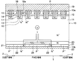
第1実施形態について図面を参照しつつ説明する。なお、本実施形態の半導体装置は、例えば、インバータ、DC/DCコンバータ等の電源回路に使用されるパワースイッチング素子として利用されると好適である。
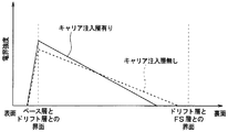
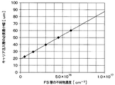
したがって、本実施形態では、キャリア注入層24およびFS層20は、上記数式を満たすように構成されている。
本発明は上記した実施形態に限定されるものではなく、特許請求の範囲に記載した範囲内において適宜変更が可能である。
1a IGBT素子
2 FWD領域
2a FWD素子
10 半導体基板
11 ドリフト層
12 ベース層
14 エミッタ領域
16 ゲート絶縁膜
17 ゲート電極
19 第1電極
20 フィールドストップ層
21 コレクタ層
22 カソード層
23 第2電極
24 キャリア注入層
Claims (4)
- IGBT素子(1a)を有するIGBT領域(1)と、FWD素子(2a)を有するFWD領域(2)が共通の半導体基板(10)に形成されている半導体装置において、
第1導電型のドリフト層(11)と、
前記ドリフト層上に形成された第2導電型のベース層(12)と、
前記ベース層の表層部であって、前記ベース層を挟んで前記ドリフト層から離間して形成され、前記ドリフト層よりも高不純物濃度とされた第1導電型のエミッタ領域(14)と、
前記エミッタ領域と前記ドリフト層との間に位置する前記ベース層の表面に配置されたゲート絶縁膜(16)と、
前記ゲート絶縁膜上に配置されたゲート電極(17)と、
前記ドリフト層を挟んで前記ベース層と反対側に配置され、前記ドリフト層よりも高不純物濃度とされた第1導電型のフィールドストップ層(20)と、
前記フィールドストップ層を挟んで前記ドリフト層と反対側に配置された第2導電型のコレクタ層(21)と、
前記フィールドストップ層を挟んで前記ドリフト層と反対側に配置されると共に前記コレクタ層と隣接するカソード層(22)と、
前記ベース層および前記エミッタ領域と電気的に接続される第1電極(19)と、
前記コレクタ層および前記カソード層と電気的に接続される第2電極(23)と、を備え、
前記カソード層には、前記コレクタ層と離れた位置に、前記第2電極と電気的に接続されると共に前記フィールドストップ層とPN接合を構成する第2導電型のキャリア注入層(24)が形成されており、
前記FWD素子に順方向電流が流れている状態から当該電流を遮断する際、前記FWD素子内の第1キャリアが前記キャリア注入層上に位置する前記フィールドストップ層を通過して前記カソード層へと流れることにより、前記第2電極から前記キャリア注入層を介して第2キャリアが前記ドリフト層に注入される半導体装置。 - 前記キャリア注入層は、前記カソード層に1つのみ形成されている請求項1に記載の半導体装置。
- 前記キャリア注入層は、前記カソード層の中心を含んで形成されている請求項1または2に記載の半導体装置。
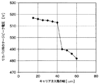
- 前記キャリア注入層は、前記半導体基板の平面方向における一方向に沿って延設されており、前記フィールドストップ層の不純物濃度をNfs[cm−3]とし、前記キャリア注入層における延設方向と直交する方向であり、前記半導体基板の平面方向に沿った方向の長さを幅W[μm]とすると、W>6.8×10⁻¹⁶×Nfs+20を満たす請求項3に記載の半導体装置。
Priority Applications (4)
| Application Number | Priority Date | Filing Date | Title |
|---|---|---|---|
| JP2016098875A JP2017208413A (ja) | 2016-05-17 | 2016-05-17 | 半導体装置 |
| PCT/JP2017/015874 WO2017199679A1 (ja) | 2016-05-17 | 2017-04-20 | 半導体装置 |
| CN201780029794.6A CN109155334B (zh) | 2016-05-17 | 2017-04-20 | 半导体装置 |
| US16/188,533 US11217580B2 (en) | 2016-05-17 | 2018-11-13 | Semiconductor device including insulated gate bipolar transistor element and freewheeling diode element |
Applications Claiming Priority (1)
| Application Number | Priority Date | Filing Date | Title |
|---|---|---|---|
| JP2016098875A JP2017208413A (ja) | 2016-05-17 | 2016-05-17 | 半導体装置 |
Publications (2)
| Publication Number | Publication Date |
|---|---|
| JP2017208413A true JP2017208413A (ja) | 2017-11-24 |
| JP2017208413A5 JP2017208413A5 (ja) | 2018-08-30 |
Family
ID=60325161
Family Applications (1)
| Application Number | Title | Priority Date | Filing Date |
|---|---|---|---|
| JP2016098875A Pending JP2017208413A (ja) | 2016-05-17 | 2016-05-17 | 半導体装置 |
Country Status (4)
| Country | Link |
|---|---|
| US (1) | US11217580B2 (ja) |
| JP (1) | JP2017208413A (ja) |
| CN (1) | CN109155334B (ja) |
| WO (1) | WO2017199679A1 (ja) |
Cited By (1)
| Publication number | Priority date | Publication date | Assignee | Title |
|---|---|---|---|---|
| CN112689902A (zh) * | 2018-09-13 | 2021-04-20 | 株式会社电装 | 半导体装置 |
Families Citing this family (10)
| Publication number | Priority date | Publication date | Assignee | Title |
|---|---|---|---|---|
| JP6935731B2 (ja) | 2017-11-16 | 2021-09-15 | 株式会社デンソー | 半導体装置 |
| CN110137249A (zh) * | 2018-02-09 | 2019-08-16 | 苏州东微半导体有限公司 | Igbt功率器件及其制造方法 |
| CN112470288A (zh) | 2019-02-27 | 2021-03-09 | 富士电机株式会社 | 半导体装置 |
| US12057416B2 (en) * | 2019-04-08 | 2024-08-06 | Sumitomo Electric Industries, Ltd. | Semiconductor device with metal film on surface between passivation film and copper film |
| GB2584698B (en) * | 2019-06-12 | 2022-09-14 | Mqsemi Ag | Non-punch-through reverse-conducting power semiconductor device and method for producing same |
| CN110797403B (zh) * | 2019-10-18 | 2023-08-01 | 上海睿驱微电子科技有限公司 | 一种rc-igbt半导体装置 |
| CN110797404B (zh) * | 2019-10-18 | 2023-11-28 | 上海睿驱微电子科技有限公司 | 一种rc-igbt半导体器件 |
| DE102020123847A1 (de) * | 2020-09-14 | 2022-03-17 | Infineon Technologies Ag | Feldstoppgebiet enthaltende leistungs-halbleiterdiode |
| CN116632053B (zh) * | 2023-07-25 | 2024-01-30 | 深圳市美浦森半导体有限公司 | 一种rc-igbt器件的控制方法 |
| CN117650165B (zh) * | 2023-10-31 | 2024-05-31 | 海信家电集团股份有限公司 | 半导体装置 |
Citations (3)
| Publication number | Priority date | Publication date | Assignee | Title |
|---|---|---|---|---|
| JP2013021142A (ja) * | 2011-07-12 | 2013-01-31 | Toyota Central R&D Labs Inc | 半導体装置 |
| JP2013080796A (ja) * | 2011-10-03 | 2013-05-02 | Toyota Central R&D Labs Inc | 半導体装置 |
| JP2014103376A (ja) * | 2012-09-24 | 2014-06-05 | Toshiba Corp | 半導体装置 |
Family Cites Families (8)
| Publication number | Priority date | Publication date | Assignee | Title |
|---|---|---|---|---|
| JP5157201B2 (ja) | 2006-03-22 | 2013-03-06 | 株式会社デンソー | 半導体装置 |
| JP5678469B2 (ja) | 2010-05-07 | 2015-03-04 | 株式会社デンソー | 半導体装置 |
| JP5582102B2 (ja) * | 2010-07-01 | 2014-09-03 | 株式会社デンソー | 半導体装置 |
| JP5321669B2 (ja) | 2010-11-25 | 2013-10-23 | 株式会社デンソー | 半導体装置 |
| JP2013235891A (ja) | 2012-05-07 | 2013-11-21 | Denso Corp | 半導体装置 |
| JP5981859B2 (ja) | 2013-02-15 | 2016-08-31 | 株式会社豊田中央研究所 | ダイオード及びダイオードを内蔵する半導体装置 |
| JP6158123B2 (ja) * | 2014-03-14 | 2017-07-05 | 株式会社東芝 | 半導体装置 |
| DE112014007266B4 (de) * | 2014-12-17 | 2024-05-29 | Mitsubishi Electric Corporation | Halbleitervorrichtung |
-
2016
- 2016-05-17 JP JP2016098875A patent/JP2017208413A/ja active Pending
-
2017
- 2017-04-20 WO PCT/JP2017/015874 patent/WO2017199679A1/ja active Application Filing
- 2017-04-20 CN CN201780029794.6A patent/CN109155334B/zh active Active
-
2018
- 2018-11-13 US US16/188,533 patent/US11217580B2/en active Active
Patent Citations (3)
| Publication number | Priority date | Publication date | Assignee | Title |
|---|---|---|---|---|
| JP2013021142A (ja) * | 2011-07-12 | 2013-01-31 | Toyota Central R&D Labs Inc | 半導体装置 |
| JP2013080796A (ja) * | 2011-10-03 | 2013-05-02 | Toyota Central R&D Labs Inc | 半導体装置 |
| JP2014103376A (ja) * | 2012-09-24 | 2014-06-05 | Toshiba Corp | 半導体装置 |
Cited By (1)
| Publication number | Priority date | Publication date | Assignee | Title |
|---|---|---|---|---|
| CN112689902A (zh) * | 2018-09-13 | 2021-04-20 | 株式会社电装 | 半导体装置 |
Also Published As
| Publication number | Publication date |
|---|---|
| CN109155334A (zh) | 2019-01-04 |
| US20190081163A1 (en) | 2019-03-14 |
| US11217580B2 (en) | 2022-01-04 |
| CN109155334B (zh) | 2021-11-05 |
| WO2017199679A1 (ja) | 2017-11-23 |
Similar Documents
| Publication | Publication Date | Title |
|---|---|---|
| JP6791312B2 (ja) | 半導体装置 | |
| WO2017199679A1 (ja) | 半導体装置 | |
| JP6443267B2 (ja) | 半導体装置 | |
| CN109964317B (zh) | 半导体装置 | |
| JP6459791B2 (ja) | 半導体装置およびその製造方法 | |
| JP6641983B2 (ja) | 半導体装置 | |
| JP5787853B2 (ja) | 電力用半導体装置 | |
| JP2005317751A (ja) | 逆導通型半導体素子とその製造方法 | |
| JP2008053648A (ja) | 絶縁ゲート型半導体装置及びその製造方法 | |
| JP2015103697A (ja) | 半導体装置 | |
| JP2007134625A (ja) | 半導体装置およびその製造方法 | |
| CN109509789B (zh) | 半导体装置 | |
| JP2016157934A (ja) | 半導体装置 | |
| JP5537359B2 (ja) | 半導体装置 | |
| JP2016092163A (ja) | 半導体装置 | |
| US20170309704A1 (en) | Semiconductor device and manufacturing method therefor | |
| JP2011238681A (ja) | 半導体装置 | |
| US11289476B2 (en) | Semiconductor device including carrier injection layers | |
| JP2020043237A (ja) | 半導体装置 | |
| JP7172920B2 (ja) | 半導体装置 | |
| JP2021174924A (ja) | 半導体装置 | |
| JP5151175B2 (ja) | 半導体装置 | |
| WO2018230312A1 (ja) | 半導体装置 | |
| JP2018125490A (ja) | 半導体装置 | |
| JP2008182032A (ja) | 半導体装置 |
Legal Events
| Date | Code | Title | Description |
|---|---|---|---|
| A521 | Request for written amendment filed |
Free format text: JAPANESE INTERMEDIATE CODE: A523 Effective date: 20180713 |
|
| A621 | Written request for application examination |
Free format text: JAPANESE INTERMEDIATE CODE: A621 Effective date: 20180713 |
|
| A131 | Notification of reasons for refusal |
Free format text: JAPANESE INTERMEDIATE CODE: A131 Effective date: 20190305 |
|
| A521 | Request for written amendment filed |
Free format text: JAPANESE INTERMEDIATE CODE: A523 Effective date: 20190425 |
|
| A131 | Notification of reasons for refusal |
Free format text: JAPANESE INTERMEDIATE CODE: A131 Effective date: 20190903 |
|
| A02 | Decision of refusal |
Free format text: JAPANESE INTERMEDIATE CODE: A02 Effective date: 20200331 |


