JP4698251B2 - 可動又は柔軟なシャワーヘッド取り付け - Google Patents
可動又は柔軟なシャワーヘッド取り付け Download PDFInfo
- Publication number
- JP4698251B2 JP4698251B2 JP2005045994A JP2005045994A JP4698251B2 JP 4698251 B2 JP4698251 B2 JP 4698251B2 JP 2005045994 A JP2005045994 A JP 2005045994A JP 2005045994 A JP2005045994 A JP 2005045994A JP 4698251 B2 JP4698251 B2 JP 4698251B2
- Authority
- JP
- Japan
- Prior art keywords
- showerhead
- gas
- gas inlet
- shower head
- inlet manifold
- Prior art date
- Legal status (The legal status is an assumption and is not a legal conclusion. Google has not performed a legal analysis and makes no representation as to the accuracy of the status listed.)
- Expired - Lifetime
Links
Images


Classifications
-
- F—MECHANICAL ENGINEERING; LIGHTING; HEATING; WEAPONS; BLASTING
- F16—ENGINEERING ELEMENTS AND UNITS; GENERAL MEASURES FOR PRODUCING AND MAINTAINING EFFECTIVE FUNCTIONING OF MACHINES OR INSTALLATIONS; THERMAL INSULATION IN GENERAL
- F16B—DEVICES FOR FASTENING OR SECURING CONSTRUCTIONAL ELEMENTS OR MACHINE PARTS TOGETHER, e.g. NAILS, BOLTS, CIRCLIPS, CLAMPS, CLIPS OR WEDGES; JOINTS OR JOINTING
- F16B35/00—Screw-bolts; Stay-bolts; Screw-threaded studs; Screws; Set screws
- F16B35/04—Screw-bolts; Stay-bolts; Screw-threaded studs; Screws; Set screws with specially-shaped head or shaft in order to fix the bolt on or in an object
- F16B35/041—Specially-shaped shafts
- F16B35/044—Specially-shaped ends
-
- C—CHEMISTRY; METALLURGY
- C23—COATING METALLIC MATERIAL; COATING MATERIAL WITH METALLIC MATERIAL; CHEMICAL SURFACE TREATMENT; DIFFUSION TREATMENT OF METALLIC MATERIAL; COATING BY VACUUM EVAPORATION, BY SPUTTERING, BY ION IMPLANTATION OR BY CHEMICAL VAPOUR DEPOSITION, IN GENERAL; INHIBITING CORROSION OF METALLIC MATERIAL OR INCRUSTATION IN GENERAL
- C23C—COATING METALLIC MATERIAL; COATING MATERIAL WITH METALLIC MATERIAL; SURFACE TREATMENT OF METALLIC MATERIAL BY DIFFUSION INTO THE SURFACE, BY CHEMICAL CONVERSION OR SUBSTITUTION; COATING BY VACUUM EVAPORATION, BY SPUTTERING, BY ION IMPLANTATION OR BY CHEMICAL VAPOUR DEPOSITION, IN GENERAL
- C23C16/00—Chemical coating by decomposition of gaseous compounds, without leaving reaction products of surface material in the coating, i.e. chemical vapour deposition [CVD] processes
- C23C16/44—Chemical coating by decomposition of gaseous compounds, without leaving reaction products of surface material in the coating, i.e. chemical vapour deposition [CVD] processes characterised by the method of coating
- C23C16/455—Chemical coating by decomposition of gaseous compounds, without leaving reaction products of surface material in the coating, i.e. chemical vapour deposition [CVD] processes characterised by the method of coating characterised by the method used for introducing gases into reaction chamber or for modifying gas flows in reaction chamber
- C23C16/45563—Gas nozzles
- C23C16/45565—Shower nozzles
-
- B—PERFORMING OPERATIONS; TRANSPORTING
- B65—CONVEYING; PACKING; STORING; HANDLING THIN OR FILAMENTARY MATERIAL
- B65D—CONTAINERS FOR STORAGE OR TRANSPORT OF ARTICLES OR MATERIALS, e.g. BAGS, BARRELS, BOTTLES, BOXES, CANS, CARTONS, CRATES, DRUMS, JARS, TANKS, HOPPERS, FORWARDING CONTAINERS; ACCESSORIES, CLOSURES, OR FITTINGS THEREFOR; PACKAGING ELEMENTS; PACKAGES
- B65D19/00—Pallets or like platforms, with or without side walls, for supporting loads to be lifted or lowered
- B65D19/38—Details or accessories
- B65D19/385—Frames, corner posts or pallet converters, e.g. for facilitating stacking of charged pallets
-
- H—ELECTRICITY
- H01—ELECTRIC ELEMENTS
- H01J—ELECTRIC DISCHARGE TUBES OR DISCHARGE LAMPS
- H01J37/00—Discharge tubes with provision for introducing objects or material to be exposed to the discharge, e.g. for the purpose of examination or processing thereof
- H01J37/32—Gas-filled discharge tubes
- H01J37/32431—Constructional details of the reactor
- H01J37/3244—Gas supply means
-
- H—ELECTRICITY
- H01—ELECTRIC ELEMENTS
- H01J—ELECTRIC DISCHARGE TUBES OR DISCHARGE LAMPS
- H01J37/00—Discharge tubes with provision for introducing objects or material to be exposed to the discharge, e.g. for the purpose of examination or processing thereof
- H01J37/32—Gas-filled discharge tubes
- H01J37/32431—Constructional details of the reactor
- H01J37/32458—Vessel
- H01J37/32522—Temperature
Landscapes
- Chemical & Material Sciences (AREA)
- Engineering & Computer Science (AREA)
- Physics & Mathematics (AREA)
- Plasma & Fusion (AREA)
- Analytical Chemistry (AREA)
- Mechanical Engineering (AREA)
- Materials Engineering (AREA)
- Chemical Kinetics & Catalysis (AREA)
- General Chemical & Material Sciences (AREA)
- Metallurgy (AREA)
- Organic Chemistry (AREA)
- General Engineering & Computer Science (AREA)
- Chemical Vapour Deposition (AREA)
- Drying Of Semiconductors (AREA)
- Fire-Extinguishing By Fire Departments, And Fire-Extinguishing Equipment And Control Thereof (AREA)
- Nozzles (AREA)
Applications Claiming Priority (2)
| Application Number | Priority Date | Filing Date | Title |
|---|---|---|---|
| US54733804P | 2004-02-24 | 2004-02-24 | |
| US60/547338 | 2004-02-24 |
Related Child Applications (1)
| Application Number | Title | Priority Date | Filing Date |
|---|---|---|---|
| JP2010278191A Division JP5366923B2 (ja) | 2004-02-24 | 2010-12-14 | 可動又は柔軟なシャワーヘッド取り付け |
Publications (3)
| Publication Number | Publication Date |
|---|---|
| JP2005256172A JP2005256172A (ja) | 2005-09-22 |
| JP2005256172A5 JP2005256172A5 (https=) | 2008-04-24 |
| JP4698251B2 true JP4698251B2 (ja) | 2011-06-08 |
Family
ID=35046181
Family Applications (2)
| Application Number | Title | Priority Date | Filing Date |
|---|---|---|---|
| JP2005045994A Expired - Lifetime JP4698251B2 (ja) | 2004-02-24 | 2005-02-22 | 可動又は柔軟なシャワーヘッド取り付け |
| JP2010278191A Expired - Lifetime JP5366923B2 (ja) | 2004-02-24 | 2010-12-14 | 可動又は柔軟なシャワーヘッド取り付け |
Family Applications After (1)
| Application Number | Title | Priority Date | Filing Date |
|---|---|---|---|
| JP2010278191A Expired - Lifetime JP5366923B2 (ja) | 2004-02-24 | 2010-12-14 | 可動又は柔軟なシャワーヘッド取り付け |
Country Status (5)
| Country | Link |
|---|---|
| US (1) | US7722925B2 (https=) |
| JP (2) | JP4698251B2 (https=) |
| KR (1) | KR100769963B1 (https=) |
| CN (2) | CN102212798B (https=) |
| TW (1) | TWI290962B (https=) |
Cited By (1)
| Publication number | Priority date | Publication date | Assignee | Title |
|---|---|---|---|---|
| KR101529669B1 (ko) * | 2008-06-12 | 2015-06-18 | 주성엔지니어링(주) | 기판처리장치 |
Families Citing this family (551)
| Publication number | Priority date | Publication date | Assignee | Title |
|---|---|---|---|---|
| US6477980B1 (en) * | 2000-01-20 | 2002-11-12 | Applied Materials, Inc. | Flexibly suspended gas distribution manifold for plasma chamber |
| US6772827B2 (en) * | 2000-01-20 | 2004-08-10 | Applied Materials, Inc. | Suspended gas distribution manifold for plasma chamber |
| KR100490049B1 (ko) * | 2003-04-14 | 2005-05-17 | 삼성전자주식회사 | 일체형 디퓨저 프레임을 가지는 cvd 장치 |
| US8083853B2 (en) * | 2004-05-12 | 2011-12-27 | Applied Materials, Inc. | Plasma uniformity control by gas diffuser hole design |
| US7712434B2 (en) * | 2004-04-30 | 2010-05-11 | Lam Research Corporation | Apparatus including showerhead electrode and heater for plasma processing |
| US8328939B2 (en) * | 2004-05-12 | 2012-12-11 | Applied Materials, Inc. | Diffuser plate with slit valve compensation |
| US8074599B2 (en) * | 2004-05-12 | 2011-12-13 | Applied Materials, Inc. | Plasma uniformity control by gas diffuser curvature |
| US7429410B2 (en) | 2004-09-20 | 2008-09-30 | Applied Materials, Inc. | Diffuser gravity support |
| US7641762B2 (en) * | 2005-09-02 | 2010-01-05 | Applied Materials, Inc. | Gas sealing skirt for suspended showerhead in process chamber |
| TWI306782B (en) * | 2005-09-02 | 2009-03-01 | Applied Materials Inc | Suspension for showerhead in process chamber |
| JP5044931B2 (ja) * | 2005-10-31 | 2012-10-10 | 東京エレクトロン株式会社 | ガス供給装置及び基板処理装置 |
| US7476291B2 (en) * | 2006-09-28 | 2009-01-13 | Lam Research Corporation | High chamber temperature process and chamber design for photo-resist stripping and post-metal etch passivation |
| US7776178B2 (en) * | 2006-10-25 | 2010-08-17 | Applied Materials, Inc. | Suspension for showerhead in process chamber |
| US7674394B2 (en) | 2007-02-26 | 2010-03-09 | Applied Materials, Inc. | Plasma process for inductively coupling power through a gas distribution plate while adjusting plasma distribution |
| KR100801711B1 (ko) * | 2007-02-27 | 2008-02-11 | 삼성전자주식회사 | 반도체 식각 및 증착 공정들을 수행하는 반도체 제조장비들 및 그를 이용한 반도체 소자의 형성방법들 |
| US20080236495A1 (en) * | 2007-03-27 | 2008-10-02 | Structured Materials Inc. | Showerhead for chemical vapor deposition (CVD) apparatus |
| US20080317973A1 (en) * | 2007-06-22 | 2008-12-25 | White John M | Diffuser support |
| WO2009078921A1 (en) * | 2007-12-19 | 2009-06-25 | Applied Materials, Inc. | Plasma reactor gas distribution plate with path splitting manifold |
| US8512509B2 (en) | 2007-12-19 | 2013-08-20 | Applied Materials, Inc. | Plasma reactor gas distribution plate with radially distributed path splitting manifold |
| JP5524076B2 (ja) * | 2007-12-25 | 2014-06-18 | アプライド マテリアルズ インコーポレイテッド | プラズマチャンバへrf電力を結合する装置 |
| WO2010044895A2 (en) * | 2008-01-31 | 2010-04-22 | Applied Materials, Inc | Multiple phase rf power for electrode of plasma chamber |
| KR100970201B1 (ko) * | 2008-03-17 | 2010-07-14 | 주식회사 아이피에스 | 진공처리장치 |
| US8373092B2 (en) * | 2008-04-09 | 2013-02-12 | The Boeing Company | Purge and sealant cap for selective laser sintering build frame |
| US20090258162A1 (en) * | 2008-04-12 | 2009-10-15 | Applied Materials, Inc. | Plasma processing apparatus and method |
| KR101569752B1 (ko) | 2008-06-12 | 2015-11-19 | 주성엔지니어링(주) | 기판처리장치 |
| WO2010051233A2 (en) * | 2008-10-31 | 2010-05-06 | Applied Materials, Inc. | Adjustable gas distribution apparatus |
| US9328417B2 (en) * | 2008-11-01 | 2016-05-03 | Ultratech, Inc. | System and method for thin film deposition |
| WO2010094002A2 (en) * | 2009-02-13 | 2010-08-19 | Applied Materials, Inc. | Rf bus and rf return bus for plasma chamber electrode |
| KR101190750B1 (ko) * | 2009-02-19 | 2012-10-12 | 엘지전자 주식회사 | 실리콘 박막 제조방법 및 제조장치 |
| KR101687955B1 (ko) * | 2009-02-22 | 2016-12-20 | 마퍼 리쏘그라피 아이피 비.브이. | 하전입자 리소그래피 장치 및 진공 챔버에 진공을 발생시키는 방법 |
| US9394608B2 (en) | 2009-04-06 | 2016-07-19 | Asm America, Inc. | Semiconductor processing reactor and components thereof |
| KR101099533B1 (ko) | 2009-07-23 | 2011-12-28 | 세메스 주식회사 | 기판 처리 유닛 및 장치 |
| US8802201B2 (en) | 2009-08-14 | 2014-08-12 | Asm America, Inc. | Systems and methods for thin-film deposition of metal oxides using excited nitrogen-oxygen species |
| US9039864B2 (en) * | 2009-09-29 | 2015-05-26 | Applied Materials, Inc. | Off-center ground return for RF-powered showerhead |
| TWI430714B (zh) * | 2009-10-15 | 2014-03-11 | Orbotech Lt Solar Llc | 電漿處理腔之噴撒頭組件及電漿處理腔之噴撒頭組件之氣體電離板之製備方法 |
| JP5835722B2 (ja) * | 2009-12-10 | 2015-12-24 | オルボテック エルティ ソラー,エルエルシー | 自動順位付け多方向直列型処理装置 |
| US9850576B2 (en) * | 2010-02-15 | 2017-12-26 | Applied Materials, Inc. | Anti-arc zero field plate |
| WO2011146571A2 (en) * | 2010-05-21 | 2011-11-24 | Applied Materials, Inc. | Tightly-fitted ceramic insulator on large-area electrode |
| US9324576B2 (en) | 2010-05-27 | 2016-04-26 | Applied Materials, Inc. | Selective etch for silicon films |
| JP2012216744A (ja) * | 2010-11-10 | 2012-11-08 | Sharp Corp | 気相成長装置及び気相成長方法 |
| US8741778B2 (en) | 2010-12-14 | 2014-06-03 | Applied Materials, Inc. | Uniform dry etch in two stages |
| US10283321B2 (en) | 2011-01-18 | 2019-05-07 | Applied Materials, Inc. | Semiconductor processing system and methods using capacitively coupled plasma |
| US8771539B2 (en) | 2011-02-22 | 2014-07-08 | Applied Materials, Inc. | Remotely-excited fluorine and water vapor etch |
| WO2012148568A1 (en) | 2011-03-01 | 2012-11-01 | Applied Materials, Inc. | Method and apparatus for substrate transfer and radical confinement |
| US11171008B2 (en) * | 2011-03-01 | 2021-11-09 | Applied Materials, Inc. | Abatement and strip process chamber in a dual load lock configuration |
| KR101895307B1 (ko) | 2011-03-01 | 2018-10-04 | 어플라이드 머티어리얼스, 인코포레이티드 | 듀얼 로드락 구성의 저감 및 스트립 프로세스 챔버 |
| US20120231181A1 (en) * | 2011-03-09 | 2012-09-13 | Applied Materials, Inc. | Insulation coverage of cvd electrode |
| US9064815B2 (en) | 2011-03-14 | 2015-06-23 | Applied Materials, Inc. | Methods for etch of metal and metal-oxide films |
| US8999856B2 (en) | 2011-03-14 | 2015-04-07 | Applied Materials, Inc. | Methods for etch of sin films |
| CN102154691B (zh) * | 2011-05-30 | 2012-11-21 | 东莞市中镓半导体科技有限公司 | 狭缝式多气体输运喷头结构 |
| US9312155B2 (en) | 2011-06-06 | 2016-04-12 | Asm Japan K.K. | High-throughput semiconductor-processing apparatus equipped with multiple dual-chamber modules |
| JP5753450B2 (ja) * | 2011-06-30 | 2015-07-22 | 東京エレクトロン株式会社 | 成膜装置 |
| US10854498B2 (en) | 2011-07-15 | 2020-12-01 | Asm Ip Holding B.V. | Wafer-supporting device and method for producing same |
| US20130023129A1 (en) | 2011-07-20 | 2013-01-24 | Asm America, Inc. | Pressure transmitter for a semiconductor processing environment |
| US8771536B2 (en) | 2011-08-01 | 2014-07-08 | Applied Materials, Inc. | Dry-etch for silicon-and-carbon-containing films |
| US8679982B2 (en) | 2011-08-26 | 2014-03-25 | Applied Materials, Inc. | Selective suppression of dry-etch rate of materials containing both silicon and oxygen |
| US8679983B2 (en) | 2011-09-01 | 2014-03-25 | Applied Materials, Inc. | Selective suppression of dry-etch rate of materials containing both silicon and nitrogen |
| US8927390B2 (en) | 2011-09-26 | 2015-01-06 | Applied Materials, Inc. | Intrench profile |
| US8808563B2 (en) | 2011-10-07 | 2014-08-19 | Applied Materials, Inc. | Selective etch of silicon by way of metastable hydrogen termination |
| US9017481B1 (en) | 2011-10-28 | 2015-04-28 | Asm America, Inc. | Process feed management for semiconductor substrate processing |
| WO2013070436A1 (en) | 2011-11-08 | 2013-05-16 | Applied Materials, Inc. | Methods of reducing substrate dislocation during gapfill processing |
| CN106847737B (zh) | 2012-02-29 | 2020-11-13 | 应用材料公司 | 配置中的除污及剥除处理腔室 |
| US9267739B2 (en) | 2012-07-18 | 2016-02-23 | Applied Materials, Inc. | Pedestal with multi-zone temperature control and multiple purge capabilities |
| US9373517B2 (en) | 2012-08-02 | 2016-06-21 | Applied Materials, Inc. | Semiconductor processing with DC assisted RF power for improved control |
| US9034770B2 (en) | 2012-09-17 | 2015-05-19 | Applied Materials, Inc. | Differential silicon oxide etch |
| US9023734B2 (en) | 2012-09-18 | 2015-05-05 | Applied Materials, Inc. | Radical-component oxide etch |
| US9390937B2 (en) | 2012-09-20 | 2016-07-12 | Applied Materials, Inc. | Silicon-carbon-nitride selective etch |
| US9132436B2 (en) | 2012-09-21 | 2015-09-15 | Applied Materials, Inc. | Chemical control features in wafer process equipment |
| US10714315B2 (en) | 2012-10-12 | 2020-07-14 | Asm Ip Holdings B.V. | Semiconductor reaction chamber showerhead |
| US8765574B2 (en) | 2012-11-09 | 2014-07-01 | Applied Materials, Inc. | Dry etch process |
| US8969212B2 (en) | 2012-11-20 | 2015-03-03 | Applied Materials, Inc. | Dry-etch selectivity |
| US8980763B2 (en) | 2012-11-30 | 2015-03-17 | Applied Materials, Inc. | Dry-etch for selective tungsten removal |
| US9064816B2 (en) | 2012-11-30 | 2015-06-23 | Applied Materials, Inc. | Dry-etch for selective oxidation removal |
| US9111877B2 (en) | 2012-12-18 | 2015-08-18 | Applied Materials, Inc. | Non-local plasma oxide etch |
| US8921234B2 (en) | 2012-12-21 | 2014-12-30 | Applied Materials, Inc. | Selective titanium nitride etching |
| US20160376700A1 (en) | 2013-02-01 | 2016-12-29 | Asm Ip Holding B.V. | System for treatment of deposition reactor |
| US10256079B2 (en) | 2013-02-08 | 2019-04-09 | Applied Materials, Inc. | Semiconductor processing systems having multiple plasma configurations |
| US9362130B2 (en) | 2013-03-01 | 2016-06-07 | Applied Materials, Inc. | Enhanced etching processes using remote plasma sources |
| US9040422B2 (en) | 2013-03-05 | 2015-05-26 | Applied Materials, Inc. | Selective titanium nitride removal |
| US8801952B1 (en) | 2013-03-07 | 2014-08-12 | Applied Materials, Inc. | Conformal oxide dry etch |
| US10170282B2 (en) | 2013-03-08 | 2019-01-01 | Applied Materials, Inc. | Insulated semiconductor faceplate designs |
| US20140271097A1 (en) | 2013-03-15 | 2014-09-18 | Applied Materials, Inc. | Processing systems and methods for halide scavenging |
| US8895449B1 (en) | 2013-05-16 | 2014-11-25 | Applied Materials, Inc. | Delicate dry clean |
| US9114438B2 (en) | 2013-05-21 | 2015-08-25 | Applied Materials, Inc. | Copper residue chamber clean |
| CN103266310B (zh) * | 2013-05-24 | 2015-05-20 | 上海和辉光电有限公司 | 分散板及具有该分散板的镀膜装置 |
| US10808317B2 (en) | 2013-07-03 | 2020-10-20 | Lam Research Corporation | Deposition apparatus including an isothermal processing zone |
| US9493879B2 (en) | 2013-07-12 | 2016-11-15 | Applied Materials, Inc. | Selective sputtering for pattern transfer |
| US9773648B2 (en) | 2013-08-30 | 2017-09-26 | Applied Materials, Inc. | Dual discharge modes operation for remote plasma |
| US8956980B1 (en) | 2013-09-16 | 2015-02-17 | Applied Materials, Inc. | Selective etch of silicon nitride |
| US8951429B1 (en) | 2013-10-29 | 2015-02-10 | Applied Materials, Inc. | Tungsten oxide processing |
| US9576809B2 (en) | 2013-11-04 | 2017-02-21 | Applied Materials, Inc. | Etch suppression with germanium |
| US9236265B2 (en) | 2013-11-04 | 2016-01-12 | Applied Materials, Inc. | Silicon germanium processing |
| US9520303B2 (en) | 2013-11-12 | 2016-12-13 | Applied Materials, Inc. | Aluminum selective etch |
| US9245762B2 (en) | 2013-12-02 | 2016-01-26 | Applied Materials, Inc. | Procedure for etch rate consistency |
| US9117855B2 (en) | 2013-12-04 | 2015-08-25 | Applied Materials, Inc. | Polarity control for remote plasma |
| US9287095B2 (en) | 2013-12-17 | 2016-03-15 | Applied Materials, Inc. | Semiconductor system assemblies and methods of operation |
| US9263278B2 (en) | 2013-12-17 | 2016-02-16 | Applied Materials, Inc. | Dopant etch selectivity control |
| US9190293B2 (en) | 2013-12-18 | 2015-11-17 | Applied Materials, Inc. | Even tungsten etch for high aspect ratio trenches |
| US9287134B2 (en) | 2014-01-17 | 2016-03-15 | Applied Materials, Inc. | Titanium oxide etch |
| US9396989B2 (en) | 2014-01-27 | 2016-07-19 | Applied Materials, Inc. | Air gaps between copper lines |
| US9293568B2 (en) | 2014-01-27 | 2016-03-22 | Applied Materials, Inc. | Method of fin patterning |
| US9385028B2 (en) | 2014-02-03 | 2016-07-05 | Applied Materials, Inc. | Air gap process |
| US10683571B2 (en) | 2014-02-25 | 2020-06-16 | Asm Ip Holding B.V. | Gas supply manifold and method of supplying gases to chamber using same |
| US9499898B2 (en) | 2014-03-03 | 2016-11-22 | Applied Materials, Inc. | Layered thin film heater and method of fabrication |
| US9299575B2 (en) | 2014-03-17 | 2016-03-29 | Applied Materials, Inc. | Gas-phase tungsten etch |
| US10167557B2 (en) | 2014-03-18 | 2019-01-01 | Asm Ip Holding B.V. | Gas distribution system, reactor including the system, and methods of using the same |
| US11015245B2 (en) | 2014-03-19 | 2021-05-25 | Asm Ip Holding B.V. | Gas-phase reactor and system having exhaust plenum and components thereof |
| US9299538B2 (en) | 2014-03-20 | 2016-03-29 | Applied Materials, Inc. | Radial waveguide systems and methods for post-match control of microwaves |
| US9299537B2 (en) | 2014-03-20 | 2016-03-29 | Applied Materials, Inc. | Radial waveguide systems and methods for post-match control of microwaves |
| US9136273B1 (en) | 2014-03-21 | 2015-09-15 | Applied Materials, Inc. | Flash gate air gap |
| US9903020B2 (en) | 2014-03-31 | 2018-02-27 | Applied Materials, Inc. | Generation of compact alumina passivation layers on aluminum plasma equipment components |
| US9269590B2 (en) | 2014-04-07 | 2016-02-23 | Applied Materials, Inc. | Spacer formation |
| US9309598B2 (en) | 2014-05-28 | 2016-04-12 | Applied Materials, Inc. | Oxide and metal removal |
| US9847289B2 (en) | 2014-05-30 | 2017-12-19 | Applied Materials, Inc. | Protective via cap for improved interconnect performance |
| US9378969B2 (en) | 2014-06-19 | 2016-06-28 | Applied Materials, Inc. | Low temperature gas-phase carbon removal |
| US9406523B2 (en) | 2014-06-19 | 2016-08-02 | Applied Materials, Inc. | Highly selective doped oxide removal method |
| US9425058B2 (en) | 2014-07-24 | 2016-08-23 | Applied Materials, Inc. | Simplified litho-etch-litho-etch process |
| US10858737B2 (en) | 2014-07-28 | 2020-12-08 | Asm Ip Holding B.V. | Showerhead assembly and components thereof |
| US9378978B2 (en) | 2014-07-31 | 2016-06-28 | Applied Materials, Inc. | Integrated oxide recess and floating gate fin trimming |
| US9159606B1 (en) | 2014-07-31 | 2015-10-13 | Applied Materials, Inc. | Metal air gap |
| US9496167B2 (en) | 2014-07-31 | 2016-11-15 | Applied Materials, Inc. | Integrated bit-line airgap formation and gate stack post clean |
| US9165786B1 (en) | 2014-08-05 | 2015-10-20 | Applied Materials, Inc. | Integrated oxide and nitride recess for better channel contact in 3D architectures |
| US9659753B2 (en) | 2014-08-07 | 2017-05-23 | Applied Materials, Inc. | Grooved insulator to reduce leakage current |
| US9553102B2 (en) | 2014-08-19 | 2017-01-24 | Applied Materials, Inc. | Tungsten separation |
| US9890456B2 (en) | 2014-08-21 | 2018-02-13 | Asm Ip Holding B.V. | Method and system for in situ formation of gas-phase compounds |
| US9355856B2 (en) | 2014-09-12 | 2016-05-31 | Applied Materials, Inc. | V trench dry etch |
| US9368364B2 (en) | 2014-09-24 | 2016-06-14 | Applied Materials, Inc. | Silicon etch process with tunable selectivity to SiO2 and other materials |
| US9478434B2 (en) | 2014-09-24 | 2016-10-25 | Applied Materials, Inc. | Chlorine-based hardmask removal |
| US9613822B2 (en) | 2014-09-25 | 2017-04-04 | Applied Materials, Inc. | Oxide etch selectivity enhancement |
| US10941490B2 (en) | 2014-10-07 | 2021-03-09 | Asm Ip Holding B.V. | Multiple temperature range susceptor, assembly, reactor and system including the susceptor, and methods of using the same |
| US9657845B2 (en) | 2014-10-07 | 2017-05-23 | Asm Ip Holding B.V. | Variable conductance gas distribution apparatus and method |
| US9966240B2 (en) | 2014-10-14 | 2018-05-08 | Applied Materials, Inc. | Systems and methods for internal surface conditioning assessment in plasma processing equipment |
| US9355922B2 (en) | 2014-10-14 | 2016-05-31 | Applied Materials, Inc. | Systems and methods for internal surface conditioning in plasma processing equipment |
| DE102015110440A1 (de) * | 2014-11-20 | 2016-05-25 | Aixtron Se | CVD- oder PVD-Reaktor zum Beschichten großflächiger Substrate |
| US11637002B2 (en) | 2014-11-26 | 2023-04-25 | Applied Materials, Inc. | Methods and systems to enhance process uniformity |
| US9299583B1 (en) | 2014-12-05 | 2016-03-29 | Applied Materials, Inc. | Aluminum oxide selective etch |
| US10573496B2 (en) | 2014-12-09 | 2020-02-25 | Applied Materials, Inc. | Direct outlet toroidal plasma source |
| US10224210B2 (en) | 2014-12-09 | 2019-03-05 | Applied Materials, Inc. | Plasma processing system with direct outlet toroidal plasma source |
| US9502258B2 (en) | 2014-12-23 | 2016-11-22 | Applied Materials, Inc. | Anisotropic gap etch |
| US9343272B1 (en) | 2015-01-08 | 2016-05-17 | Applied Materials, Inc. | Self-aligned process |
| US11257693B2 (en) | 2015-01-09 | 2022-02-22 | Applied Materials, Inc. | Methods and systems to improve pedestal temperature control |
| US9373522B1 (en) | 2015-01-22 | 2016-06-21 | Applied Mateials, Inc. | Titanium nitride removal |
| US9449846B2 (en) | 2015-01-28 | 2016-09-20 | Applied Materials, Inc. | Vertical gate separation |
| US20160225652A1 (en) | 2015-02-03 | 2016-08-04 | Applied Materials, Inc. | Low temperature chuck for plasma processing systems |
| US9728437B2 (en) | 2015-02-03 | 2017-08-08 | Applied Materials, Inc. | High temperature chuck for plasma processing systems |
| US9881805B2 (en) | 2015-03-02 | 2018-01-30 | Applied Materials, Inc. | Silicon selective removal |
| KR102389078B1 (ko) * | 2015-03-05 | 2022-04-22 | 주성엔지니어링(주) | 기판 처리장치에 구비되는 샤워헤드 |
| US10276355B2 (en) | 2015-03-12 | 2019-04-30 | Asm Ip Holding B.V. | Multi-zone reactor, system including the reactor, and method of using the same |
| KR20160147482A (ko) * | 2015-06-15 | 2016-12-23 | 삼성전자주식회사 | 가스 혼합부를 갖는 반도체 소자 제조 설비 |
| US10458018B2 (en) | 2015-06-26 | 2019-10-29 | Asm Ip Holding B.V. | Structures including metal carbide material, devices including the structures, and methods of forming same |
| US10600673B2 (en) | 2015-07-07 | 2020-03-24 | Asm Ip Holding B.V. | Magnetic susceptor to baseplate seal |
| US9741593B2 (en) | 2015-08-06 | 2017-08-22 | Applied Materials, Inc. | Thermal management systems and methods for wafer processing systems |
| US9691645B2 (en) | 2015-08-06 | 2017-06-27 | Applied Materials, Inc. | Bolted wafer chuck thermal management systems and methods for wafer processing systems |
| US9349605B1 (en) | 2015-08-07 | 2016-05-24 | Applied Materials, Inc. | Oxide etch selectivity systems and methods |
| US10504700B2 (en) | 2015-08-27 | 2019-12-10 | Applied Materials, Inc. | Plasma etching systems and methods with secondary plasma injection |
| US10211308B2 (en) | 2015-10-21 | 2019-02-19 | Asm Ip Holding B.V. | NbMC layers |
| JP6333232B2 (ja) * | 2015-12-02 | 2018-05-30 | 株式会社日立国際電気 | 基板処理装置、半導体装置の製造方法およびプログラム |
| JP6285411B2 (ja) * | 2015-12-25 | 2018-02-28 | 株式会社日立国際電気 | 基板処理装置、半導体装置の製造方法及びプログラム |
| US11139308B2 (en) | 2015-12-29 | 2021-10-05 | Asm Ip Holding B.V. | Atomic layer deposition of III-V compounds to form V-NAND devices |
| US10529554B2 (en) | 2016-02-19 | 2020-01-07 | Asm Ip Holding B.V. | Method for forming silicon nitride film selectively on sidewalls or flat surfaces of trenches |
| US10343920B2 (en) | 2016-03-18 | 2019-07-09 | Asm Ip Holding B.V. | Aligned carbon nanotubes |
| JP6368732B2 (ja) * | 2016-03-29 | 2018-08-01 | 株式会社日立国際電気 | 基板処理装置、半導体装置の製造方法及びプログラム |
| US10190213B2 (en) | 2016-04-21 | 2019-01-29 | Asm Ip Holding B.V. | Deposition of metal borides |
| US10865475B2 (en) | 2016-04-21 | 2020-12-15 | Asm Ip Holding B.V. | Deposition of metal borides and silicides |
| US10032628B2 (en) | 2016-05-02 | 2018-07-24 | Asm Ip Holding B.V. | Source/drain performance through conformal solid state doping |
| US10367080B2 (en) | 2016-05-02 | 2019-07-30 | Asm Ip Holding B.V. | Method of forming a germanium oxynitride film |
| US10504754B2 (en) * | 2016-05-19 | 2019-12-10 | Applied Materials, Inc. | Systems and methods for improved semiconductor etching and component protection |
| US10522371B2 (en) | 2016-05-19 | 2019-12-31 | Applied Materials, Inc. | Systems and methods for improved semiconductor etching and component protection |
| US11453943B2 (en) | 2016-05-25 | 2022-09-27 | Asm Ip Holding B.V. | Method for forming carbon-containing silicon/metal oxide or nitride film by ALD using silicon precursor and hydrocarbon precursor |
| US9865484B1 (en) | 2016-06-29 | 2018-01-09 | Applied Materials, Inc. | Selective etch using material modification and RF pulsing |
| US9859151B1 (en) | 2016-07-08 | 2018-01-02 | Asm Ip Holding B.V. | Selective film deposition method to form air gaps |
| US10612137B2 (en) | 2016-07-08 | 2020-04-07 | Asm Ip Holdings B.V. | Organic reactants for atomic layer deposition |
| US10714385B2 (en) | 2016-07-19 | 2020-07-14 | Asm Ip Holding B.V. | Selective deposition of tungsten |
| KR102532607B1 (ko) | 2016-07-28 | 2023-05-15 | 에이에스엠 아이피 홀딩 비.브이. | 기판 가공 장치 및 그 동작 방법 |
| US9887082B1 (en) | 2016-07-28 | 2018-02-06 | Asm Ip Holding B.V. | Method and apparatus for filling a gap |
| US9812320B1 (en) | 2016-07-28 | 2017-11-07 | Asm Ip Holding B.V. | Method and apparatus for filling a gap |
| US10062575B2 (en) | 2016-09-09 | 2018-08-28 | Applied Materials, Inc. | Poly directional etch by oxidation |
| US10629473B2 (en) | 2016-09-09 | 2020-04-21 | Applied Materials, Inc. | Footing removal for nitride spacer |
| US10577689B2 (en) | 2016-09-23 | 2020-03-03 | Applied Materials, Inc. | Sputtering showerhead |
| US9721789B1 (en) | 2016-10-04 | 2017-08-01 | Applied Materials, Inc. | Saving ion-damaged spacers |
| US10546729B2 (en) | 2016-10-04 | 2020-01-28 | Applied Materials, Inc. | Dual-channel showerhead with improved profile |
| US9934942B1 (en) | 2016-10-04 | 2018-04-03 | Applied Materials, Inc. | Chamber with flow-through source |
| US10062585B2 (en) | 2016-10-04 | 2018-08-28 | Applied Materials, Inc. | Oxygen compatible plasma source |
| US10062579B2 (en) | 2016-10-07 | 2018-08-28 | Applied Materials, Inc. | Selective SiN lateral recess |
| US9947549B1 (en) | 2016-10-10 | 2018-04-17 | Applied Materials, Inc. | Cobalt-containing material removal |
| US10643826B2 (en) | 2016-10-26 | 2020-05-05 | Asm Ip Holdings B.V. | Methods for thermally calibrating reaction chambers |
| US11532757B2 (en) | 2016-10-27 | 2022-12-20 | Asm Ip Holding B.V. | Deposition of charge trapping layers |
| US10714350B2 (en) | 2016-11-01 | 2020-07-14 | ASM IP Holdings, B.V. | Methods for forming a transition metal niobium nitride film on a substrate by atomic layer deposition and related semiconductor device structures |
| US10643904B2 (en) | 2016-11-01 | 2020-05-05 | Asm Ip Holdings B.V. | Methods for forming a semiconductor device and related semiconductor device structures |
| US10229833B2 (en) | 2016-11-01 | 2019-03-12 | Asm Ip Holding B.V. | Methods for forming a transition metal nitride film on a substrate by atomic layer deposition and related semiconductor device structures |
| US10134757B2 (en) | 2016-11-07 | 2018-11-20 | Asm Ip Holding B.V. | Method of processing a substrate and a device manufactured by using the method |
| US10163696B2 (en) | 2016-11-11 | 2018-12-25 | Applied Materials, Inc. | Selective cobalt removal for bottom up gapfill |
| US9768034B1 (en) | 2016-11-11 | 2017-09-19 | Applied Materials, Inc. | Removal methods for high aspect ratio structures |
| US10242908B2 (en) | 2016-11-14 | 2019-03-26 | Applied Materials, Inc. | Airgap formation with damage-free copper |
| US10026621B2 (en) | 2016-11-14 | 2018-07-17 | Applied Materials, Inc. | SiN spacer profile patterning |
| KR102546317B1 (ko) | 2016-11-15 | 2023-06-21 | 에이에스엠 아이피 홀딩 비.브이. | 기체 공급 유닛 및 이를 포함하는 기판 처리 장치 |
| KR102762543B1 (ko) | 2016-12-14 | 2025-02-05 | 에이에스엠 아이피 홀딩 비.브이. | 기판 처리 장치 |
| US11447861B2 (en) | 2016-12-15 | 2022-09-20 | Asm Ip Holding B.V. | Sequential infiltration synthesis apparatus and a method of forming a patterned structure |
| US11581186B2 (en) | 2016-12-15 | 2023-02-14 | Asm Ip Holding B.V. | Sequential infiltration synthesis apparatus |
| US10801106B2 (en) * | 2016-12-15 | 2020-10-13 | Asm Ip Holding B.V. | Shower plate structure for exhausting deposition inhibiting gas |
| KR102700194B1 (ko) | 2016-12-19 | 2024-08-28 | 에이에스엠 아이피 홀딩 비.브이. | 기판 처리 장치 |
| US10269558B2 (en) | 2016-12-22 | 2019-04-23 | Asm Ip Holding B.V. | Method of forming a structure on a substrate |
| US10566206B2 (en) | 2016-12-27 | 2020-02-18 | Applied Materials, Inc. | Systems and methods for anisotropic material breakthrough |
| US10867788B2 (en) | 2016-12-28 | 2020-12-15 | Asm Ip Holding B.V. | Method of forming a structure on a substrate |
| US11390950B2 (en) | 2017-01-10 | 2022-07-19 | Asm Ip Holding B.V. | Reactor system and method to reduce residue buildup during a film deposition process |
| US10431429B2 (en) | 2017-02-03 | 2019-10-01 | Applied Materials, Inc. | Systems and methods for radial and azimuthal control of plasma uniformity |
| US10403507B2 (en) | 2017-02-03 | 2019-09-03 | Applied Materials, Inc. | Shaped etch profile with oxidation |
| US10043684B1 (en) | 2017-02-06 | 2018-08-07 | Applied Materials, Inc. | Self-limiting atomic thermal etching systems and methods |
| US10319739B2 (en) | 2017-02-08 | 2019-06-11 | Applied Materials, Inc. | Accommodating imperfectly aligned memory holes |
| US10655221B2 (en) | 2017-02-09 | 2020-05-19 | Asm Ip Holding B.V. | Method for depositing oxide film by thermal ALD and PEALD |
| US10468261B2 (en) | 2017-02-15 | 2019-11-05 | Asm Ip Holding B.V. | Methods for forming a metallic film on a substrate by cyclical deposition and related semiconductor device structures |
| US10943834B2 (en) | 2017-03-13 | 2021-03-09 | Applied Materials, Inc. | Replacement contact process |
| US10529563B2 (en) | 2017-03-29 | 2020-01-07 | Asm Ip Holdings B.V. | Method for forming doped metal oxide films on a substrate by cyclical deposition and related semiconductor device structures |
| USD876504S1 (en) | 2017-04-03 | 2020-02-25 | Asm Ip Holding B.V. | Exhaust flow control ring for semiconductor deposition apparatus |
| US10319649B2 (en) | 2017-04-11 | 2019-06-11 | Applied Materials, Inc. | Optical emission spectroscopy (OES) for remote plasma monitoring |
| KR102457289B1 (ko) | 2017-04-25 | 2022-10-21 | 에이에스엠 아이피 홀딩 비.브이. | 박막 증착 방법 및 반도체 장치의 제조 방법 |
| US10770286B2 (en) | 2017-05-08 | 2020-09-08 | Asm Ip Holdings B.V. | Methods for selectively forming a silicon nitride film on a substrate and related semiconductor device structures |
| US10892156B2 (en) | 2017-05-08 | 2021-01-12 | Asm Ip Holding B.V. | Methods for forming a silicon nitride film on a substrate and related semiconductor device structures |
| JP7176860B6 (ja) | 2017-05-17 | 2022-12-16 | アプライド マテリアルズ インコーポレイテッド | 前駆体の流れを改善する半導体処理チャンバ |
| US11276590B2 (en) | 2017-05-17 | 2022-03-15 | Applied Materials, Inc. | Multi-zone semiconductor substrate supports |
| US11276559B2 (en) | 2017-05-17 | 2022-03-15 | Applied Materials, Inc. | Semiconductor processing chamber for multiple precursor flow |
| US10497579B2 (en) | 2017-05-31 | 2019-12-03 | Applied Materials, Inc. | Water-free etching methods |
| US10049891B1 (en) | 2017-05-31 | 2018-08-14 | Applied Materials, Inc. | Selective in situ cobalt residue removal |
| US10920320B2 (en) | 2017-06-16 | 2021-02-16 | Applied Materials, Inc. | Plasma health determination in semiconductor substrate processing reactors |
| US12040200B2 (en) | 2017-06-20 | 2024-07-16 | Asm Ip Holding B.V. | Semiconductor processing apparatus and methods for calibrating a semiconductor processing apparatus |
| US10541246B2 (en) | 2017-06-26 | 2020-01-21 | Applied Materials, Inc. | 3D flash memory cells which discourage cross-cell electrical tunneling |
| US11306395B2 (en) | 2017-06-28 | 2022-04-19 | Asm Ip Holding B.V. | Methods for depositing a transition metal nitride film on a substrate by atomic layer deposition and related deposition apparatus |
| US10685834B2 (en) | 2017-07-05 | 2020-06-16 | Asm Ip Holdings B.V. | Methods for forming a silicon germanium tin layer and related semiconductor device structures |
| US10727080B2 (en) | 2017-07-07 | 2020-07-28 | Applied Materials, Inc. | Tantalum-containing material removal |
| US10541184B2 (en) | 2017-07-11 | 2020-01-21 | Applied Materials, Inc. | Optical emission spectroscopic techniques for monitoring etching |
| US10354889B2 (en) | 2017-07-17 | 2019-07-16 | Applied Materials, Inc. | Non-halogen etching of silicon-containing materials |
| KR20190009245A (ko) | 2017-07-18 | 2019-01-28 | 에이에스엠 아이피 홀딩 비.브이. | 반도체 소자 구조물 형성 방법 및 관련된 반도체 소자 구조물 |
| US11018002B2 (en) | 2017-07-19 | 2021-05-25 | Asm Ip Holding B.V. | Method for selectively depositing a Group IV semiconductor and related semiconductor device structures |
| US10541333B2 (en) | 2017-07-19 | 2020-01-21 | Asm Ip Holding B.V. | Method for depositing a group IV semiconductor and related semiconductor device structures |
| US11374112B2 (en) | 2017-07-19 | 2022-06-28 | Asm Ip Holding B.V. | Method for depositing a group IV semiconductor and related semiconductor device structures |
| US10590535B2 (en) | 2017-07-26 | 2020-03-17 | Asm Ip Holdings B.V. | Chemical treatment, deposition and/or infiltration apparatus and method for using the same |
| TWI815813B (zh) | 2017-08-04 | 2023-09-21 | 荷蘭商Asm智慧財產控股公司 | 用於分配反應腔內氣體的噴頭總成 |
| US10170336B1 (en) | 2017-08-04 | 2019-01-01 | Applied Materials, Inc. | Methods for anisotropic control of selective silicon removal |
| US10043674B1 (en) | 2017-08-04 | 2018-08-07 | Applied Materials, Inc. | Germanium etching systems and methods |
| US10297458B2 (en) | 2017-08-07 | 2019-05-21 | Applied Materials, Inc. | Process window widening using coated parts in plasma etch processes |
| US10692741B2 (en) * | 2017-08-08 | 2020-06-23 | Asm Ip Holdings B.V. | Radiation shield |
| US10770336B2 (en) | 2017-08-08 | 2020-09-08 | Asm Ip Holding B.V. | Substrate lift mechanism and reactor including same |
| US10249524B2 (en) | 2017-08-09 | 2019-04-02 | Asm Ip Holding B.V. | Cassette holder assembly for a substrate cassette and holding member for use in such assembly |
| US11139191B2 (en) | 2017-08-09 | 2021-10-05 | Asm Ip Holding B.V. | Storage apparatus for storing cassettes for substrates and processing apparatus equipped therewith |
| US11769682B2 (en) | 2017-08-09 | 2023-09-26 | Asm Ip Holding B.V. | Storage apparatus for storing cassettes for substrates and processing apparatus equipped therewith |
| US20190048467A1 (en) * | 2017-08-10 | 2019-02-14 | Applied Materials, Inc. | Showerhead and process chamber incorporating same |
| USD900036S1 (en) | 2017-08-24 | 2020-10-27 | Asm Ip Holding B.V. | Heater electrical connector and adapter |
| US11830730B2 (en) | 2017-08-29 | 2023-11-28 | Asm Ip Holding B.V. | Layer forming method and apparatus |
| KR102491945B1 (ko) | 2017-08-30 | 2023-01-26 | 에이에스엠 아이피 홀딩 비.브이. | 기판 처리 장치 |
| US11295980B2 (en) | 2017-08-30 | 2022-04-05 | Asm Ip Holding B.V. | Methods for depositing a molybdenum metal film over a dielectric surface of a substrate by a cyclical deposition process and related semiconductor device structures |
| US11056344B2 (en) | 2017-08-30 | 2021-07-06 | Asm Ip Holding B.V. | Layer forming method |
| KR102401446B1 (ko) | 2017-08-31 | 2022-05-24 | 에이에스엠 아이피 홀딩 비.브이. | 기판 처리 장치 |
| DE202017105481U1 (de) * | 2017-09-11 | 2018-12-12 | Aixtron Se | Gaseinlassorgan für einen CVD- oder PVD-Reaktor |
| US11598003B2 (en) * | 2017-09-12 | 2023-03-07 | Applied Materials, Inc. | Substrate processing chamber having heated showerhead assembly |
| KR102630301B1 (ko) | 2017-09-21 | 2024-01-29 | 에이에스엠 아이피 홀딩 비.브이. | 침투성 재료의 순차 침투 합성 방법 처리 및 이를 이용하여 형성된 구조물 및 장치 |
| US10844484B2 (en) | 2017-09-22 | 2020-11-24 | Asm Ip Holding B.V. | Apparatus for dispensing a vapor phase reactant to a reaction chamber and related methods |
| US10658205B2 (en) | 2017-09-28 | 2020-05-19 | Asm Ip Holdings B.V. | Chemical dispensing apparatus and methods for dispensing a chemical to a reaction chamber |
| US10403504B2 (en) | 2017-10-05 | 2019-09-03 | Asm Ip Holding B.V. | Method for selectively depositing a metallic film on a substrate |
| US10319588B2 (en) | 2017-10-10 | 2019-06-11 | Asm Ip Holding B.V. | Method for depositing a metal chalcogenide on a substrate by cyclical deposition |
| US10283324B1 (en) | 2017-10-24 | 2019-05-07 | Applied Materials, Inc. | Oxygen treatment for nitride etching |
| US10128086B1 (en) | 2017-10-24 | 2018-11-13 | Applied Materials, Inc. | Silicon pretreatment for nitride removal |
| US10923344B2 (en) | 2017-10-30 | 2021-02-16 | Asm Ip Holding B.V. | Methods for forming a semiconductor structure and related semiconductor structures |
| KR102443047B1 (ko) | 2017-11-16 | 2022-09-14 | 에이에스엠 아이피 홀딩 비.브이. | 기판 처리 장치 방법 및 그에 의해 제조된 장치 |
| US10910262B2 (en) | 2017-11-16 | 2021-02-02 | Asm Ip Holding B.V. | Method of selectively depositing a capping layer structure on a semiconductor device structure |
| US11022879B2 (en) | 2017-11-24 | 2021-06-01 | Asm Ip Holding B.V. | Method of forming an enhanced unexposed photoresist layer |
| JP7214724B2 (ja) | 2017-11-27 | 2023-01-30 | エーエスエム アイピー ホールディング ビー.ブイ. | バッチ炉で利用されるウェハカセットを収納するための収納装置 |
| TWI791689B (zh) | 2017-11-27 | 2023-02-11 | 荷蘭商Asm智慧財產控股私人有限公司 | 包括潔淨迷你環境之裝置 |
| US10256112B1 (en) | 2017-12-08 | 2019-04-09 | Applied Materials, Inc. | Selective tungsten removal |
| US10903054B2 (en) | 2017-12-19 | 2021-01-26 | Applied Materials, Inc. | Multi-zone gas distribution systems and methods |
| US11328909B2 (en) | 2017-12-22 | 2022-05-10 | Applied Materials, Inc. | Chamber conditioning and removal processes |
| US10854426B2 (en) | 2018-01-08 | 2020-12-01 | Applied Materials, Inc. | Metal recess for semiconductor structures |
| US10872771B2 (en) | 2018-01-16 | 2020-12-22 | Asm Ip Holding B. V. | Method for depositing a material film on a substrate within a reaction chamber by a cyclical deposition process and related device structures |
| KR102695659B1 (ko) | 2018-01-19 | 2024-08-14 | 에이에스엠 아이피 홀딩 비.브이. | 플라즈마 보조 증착에 의해 갭 충진 층을 증착하는 방법 |
| TWI799494B (zh) | 2018-01-19 | 2023-04-21 | 荷蘭商Asm 智慧財產控股公司 | 沈積方法 |
| USD903477S1 (en) | 2018-01-24 | 2020-12-01 | Asm Ip Holdings B.V. | Metal clamp |
| US11018047B2 (en) | 2018-01-25 | 2021-05-25 | Asm Ip Holding B.V. | Hybrid lift pin |
| USD880437S1 (en) | 2018-02-01 | 2020-04-07 | Asm Ip Holding B.V. | Gas supply plate for semiconductor manufacturing apparatus |
| US11081345B2 (en) | 2018-02-06 | 2021-08-03 | Asm Ip Holding B.V. | Method of post-deposition treatment for silicon oxide film |
| US10896820B2 (en) | 2018-02-14 | 2021-01-19 | Asm Ip Holding B.V. | Method for depositing a ruthenium-containing film on a substrate by a cyclical deposition process |
| US11685991B2 (en) | 2018-02-14 | 2023-06-27 | Asm Ip Holding B.V. | Method for depositing a ruthenium-containing film on a substrate by a cyclical deposition process |
| US10731249B2 (en) | 2018-02-15 | 2020-08-04 | Asm Ip Holding B.V. | Method of forming a transition metal containing film on a substrate by a cyclical deposition process, a method for supplying a transition metal halide compound to a reaction chamber, and related vapor deposition apparatus |
| US10964512B2 (en) | 2018-02-15 | 2021-03-30 | Applied Materials, Inc. | Semiconductor processing chamber multistage mixing apparatus and methods |
| US10679870B2 (en) | 2018-02-15 | 2020-06-09 | Applied Materials, Inc. | Semiconductor processing chamber multistage mixing apparatus |
| US10658181B2 (en) | 2018-02-20 | 2020-05-19 | Asm Ip Holding B.V. | Method of spacer-defined direct patterning in semiconductor fabrication |
| KR102636427B1 (ko) | 2018-02-20 | 2024-02-13 | 에이에스엠 아이피 홀딩 비.브이. | 기판 처리 방법 및 장치 |
| US10975470B2 (en) | 2018-02-23 | 2021-04-13 | Asm Ip Holding B.V. | Apparatus for detecting or monitoring for a chemical precursor in a high temperature environment |
| TWI766433B (zh) | 2018-02-28 | 2022-06-01 | 美商應用材料股份有限公司 | 形成氣隙的系統及方法 |
| US11473195B2 (en) | 2018-03-01 | 2022-10-18 | Asm Ip Holding B.V. | Semiconductor processing apparatus and a method for processing a substrate |
| US10593560B2 (en) | 2018-03-01 | 2020-03-17 | Applied Materials, Inc. | Magnetic induction plasma source for semiconductor processes and equipment |
| US11629406B2 (en) | 2018-03-09 | 2023-04-18 | Asm Ip Holding B.V. | Semiconductor processing apparatus comprising one or more pyrometers for measuring a temperature of a substrate during transfer of the substrate |
| US10319600B1 (en) | 2018-03-12 | 2019-06-11 | Applied Materials, Inc. | Thermal silicon etch |
| US10497573B2 (en) | 2018-03-13 | 2019-12-03 | Applied Materials, Inc. | Selective atomic layer etching of semiconductor materials |
| US11114283B2 (en) | 2018-03-16 | 2021-09-07 | Asm Ip Holding B.V. | Reactor, system including the reactor, and methods of manufacturing and using same |
| KR102646467B1 (ko) | 2018-03-27 | 2024-03-11 | 에이에스엠 아이피 홀딩 비.브이. | 기판 상에 전극을 형성하는 방법 및 전극을 포함하는 반도체 소자 구조 |
| US11230766B2 (en) | 2018-03-29 | 2022-01-25 | Asm Ip Holding B.V. | Substrate processing apparatus and method |
| US11088002B2 (en) | 2018-03-29 | 2021-08-10 | Asm Ip Holding B.V. | Substrate rack and a substrate processing system and method |
| JP7140525B2 (ja) * | 2018-03-29 | 2022-09-21 | 株式会社アルバック | 真空処理装置 |
| KR102501472B1 (ko) | 2018-03-30 | 2023-02-20 | 에이에스엠 아이피 홀딩 비.브이. | 기판 처리 방법 |
| US10573527B2 (en) | 2018-04-06 | 2020-02-25 | Applied Materials, Inc. | Gas-phase selective etching systems and methods |
| KR102600229B1 (ko) | 2018-04-09 | 2023-11-10 | 에이에스엠 아이피 홀딩 비.브이. | 기판 지지 장치, 이를 포함하는 기판 처리 장치 및 기판 처리 방법 |
| US10490406B2 (en) | 2018-04-10 | 2019-11-26 | Appled Materials, Inc. | Systems and methods for material breakthrough |
| US10699879B2 (en) | 2018-04-17 | 2020-06-30 | Applied Materials, Inc. | Two piece electrode assembly with gap for plasma control |
| US10886137B2 (en) | 2018-04-30 | 2021-01-05 | Applied Materials, Inc. | Selective nitride removal |
| US12025484B2 (en) | 2018-05-08 | 2024-07-02 | Asm Ip Holding B.V. | Thin film forming method |
| TWI843623B (zh) | 2018-05-08 | 2024-05-21 | 荷蘭商Asm Ip私人控股有限公司 | 藉由循環沉積製程於基板上沉積氧化物膜之方法及相關裝置結構 |
| US12272527B2 (en) | 2018-05-09 | 2025-04-08 | Asm Ip Holding B.V. | Apparatus for use with hydrogen radicals and method of using same |
| KR20190129718A (ko) | 2018-05-11 | 2019-11-20 | 에이에스엠 아이피 홀딩 비.브이. | 기판 상에 피도핑 금속 탄화물 막을 형성하는 방법 및 관련 반도체 소자 구조 |
| KR102596988B1 (ko) | 2018-05-28 | 2023-10-31 | 에이에스엠 아이피 홀딩 비.브이. | 기판 처리 방법 및 그에 의해 제조된 장치 |
| US11718913B2 (en) | 2018-06-04 | 2023-08-08 | Asm Ip Holding B.V. | Gas distribution system and reactor system including same |
| TWI840362B (zh) | 2018-06-04 | 2024-05-01 | 荷蘭商Asm Ip私人控股有限公司 | 水氣降低的晶圓處置腔室 |
| US11286562B2 (en) | 2018-06-08 | 2022-03-29 | Asm Ip Holding B.V. | Gas-phase chemical reactor and method of using same |
| KR102568797B1 (ko) | 2018-06-21 | 2023-08-21 | 에이에스엠 아이피 홀딩 비.브이. | 기판 처리 시스템 |
| US10797133B2 (en) | 2018-06-21 | 2020-10-06 | Asm Ip Holding B.V. | Method for depositing a phosphorus doped silicon arsenide film and related semiconductor device structures |
| US11499222B2 (en) | 2018-06-27 | 2022-11-15 | Asm Ip Holding B.V. | Cyclic deposition methods for forming metal-containing material and films and structures including the metal-containing material |
| TWI871083B (zh) | 2018-06-27 | 2025-01-21 | 荷蘭商Asm Ip私人控股有限公司 | 用於形成含金屬材料之循環沉積製程 |
| KR102686758B1 (ko) | 2018-06-29 | 2024-07-18 | 에이에스엠 아이피 홀딩 비.브이. | 박막 증착 방법 및 반도체 장치의 제조 방법 |
| US10612136B2 (en) | 2018-06-29 | 2020-04-07 | ASM IP Holding, B.V. | Temperature-controlled flange and reactor system including same |
| US10388513B1 (en) | 2018-07-03 | 2019-08-20 | Asm Ip Holding B.V. | Method for depositing silicon-free carbon-containing film as gap-fill layer by pulse plasma-assisted deposition |
| US10755922B2 (en) | 2018-07-03 | 2020-08-25 | Asm Ip Holding B.V. | Method for depositing silicon-free carbon-containing film as gap-fill layer by pulse plasma-assisted deposition |
| US10872778B2 (en) | 2018-07-06 | 2020-12-22 | Applied Materials, Inc. | Systems and methods utilizing solid-phase etchants |
| US10755941B2 (en) | 2018-07-06 | 2020-08-25 | Applied Materials, Inc. | Self-limiting selective etching systems and methods |
| US10767789B2 (en) | 2018-07-16 | 2020-09-08 | Asm Ip Holding B.V. | Diaphragm valves, valve components, and methods for forming valve components |
| US10672642B2 (en) | 2018-07-24 | 2020-06-02 | Applied Materials, Inc. | Systems and methods for pedestal configuration |
| CN112368802B (zh) * | 2018-07-31 | 2025-02-28 | 应用材料公司 | 用于ald工艺的方法和设备 |
| US10923327B2 (en) * | 2018-08-01 | 2021-02-16 | Applied Materials, Inc. | Chamber liner |
| US11053591B2 (en) | 2018-08-06 | 2021-07-06 | Asm Ip Holding B.V. | Multi-port gas injection system and reactor system including same |
| US10883175B2 (en) | 2018-08-09 | 2021-01-05 | Asm Ip Holding B.V. | Vertical furnace for processing substrates and a liner for use therein |
| US10829852B2 (en) | 2018-08-16 | 2020-11-10 | Asm Ip Holding B.V. | Gas distribution device for a wafer processing apparatus |
| US11430674B2 (en) | 2018-08-22 | 2022-08-30 | Asm Ip Holding B.V. | Sensor array, apparatus for dispensing a vapor phase reactant to a reaction chamber and related methods |
| US11024523B2 (en) | 2018-09-11 | 2021-06-01 | Asm Ip Holding B.V. | Substrate processing apparatus and method |
| KR102707956B1 (ko) | 2018-09-11 | 2024-09-19 | 에이에스엠 아이피 홀딩 비.브이. | 박막 증착 방법 |
| US11049751B2 (en) | 2018-09-14 | 2021-06-29 | Asm Ip Holding B.V. | Cassette supply system to store and handle cassettes and processing apparatus equipped therewith |
| US11049755B2 (en) | 2018-09-14 | 2021-06-29 | Applied Materials, Inc. | Semiconductor substrate supports with embedded RF shield |
| US10892198B2 (en) | 2018-09-14 | 2021-01-12 | Applied Materials, Inc. | Systems and methods for improved performance in semiconductor processing |
| US11062887B2 (en) | 2018-09-17 | 2021-07-13 | Applied Materials, Inc. | High temperature RF heater pedestals |
| US11417534B2 (en) | 2018-09-21 | 2022-08-16 | Applied Materials, Inc. | Selective material removal |
| JP7369183B2 (ja) * | 2018-09-26 | 2023-10-25 | アプライド マテリアルズ インコーポレイテッド | プラズマ処理チャンバのための熱伝導スペーサ |
| CN110970344B (zh) | 2018-10-01 | 2024-10-25 | Asmip控股有限公司 | 衬底保持设备、包含所述设备的系统及其使用方法 |
| US11232963B2 (en) | 2018-10-03 | 2022-01-25 | Asm Ip Holding B.V. | Substrate processing apparatus and method |
| KR102592699B1 (ko) | 2018-10-08 | 2023-10-23 | 에이에스엠 아이피 홀딩 비.브이. | 기판 지지 유닛 및 이를 포함하는 박막 증착 장치와 기판 처리 장치 |
| US10847365B2 (en) | 2018-10-11 | 2020-11-24 | Asm Ip Holding B.V. | Method of forming conformal silicon carbide film by cyclic CVD |
| US11682560B2 (en) | 2018-10-11 | 2023-06-20 | Applied Materials, Inc. | Systems and methods for hafnium-containing film removal |
| US10811256B2 (en) | 2018-10-16 | 2020-10-20 | Asm Ip Holding B.V. | Method for etching a carbon-containing feature |
| KR102605121B1 (ko) | 2018-10-19 | 2023-11-23 | 에이에스엠 아이피 홀딩 비.브이. | 기판 처리 장치 및 기판 처리 방법 |
| KR102546322B1 (ko) | 2018-10-19 | 2023-06-21 | 에이에스엠 아이피 홀딩 비.브이. | 기판 처리 장치 및 기판 처리 방법 |
| USD948463S1 (en) | 2018-10-24 | 2022-04-12 | Asm Ip Holding B.V. | Susceptor for semiconductor substrate supporting apparatus |
| US11121002B2 (en) | 2018-10-24 | 2021-09-14 | Applied Materials, Inc. | Systems and methods for etching metals and metal derivatives |
| US12378665B2 (en) | 2018-10-26 | 2025-08-05 | Asm Ip Holding B.V. | High temperature coatings for a preclean and etch apparatus and related methods |
| US11087997B2 (en) | 2018-10-31 | 2021-08-10 | Asm Ip Holding B.V. | Substrate processing apparatus for processing substrates |
| KR102748291B1 (ko) | 2018-11-02 | 2024-12-31 | 에이에스엠 아이피 홀딩 비.브이. | 기판 지지 유닛 및 이를 포함하는 기판 처리 장치 |
| US11572620B2 (en) | 2018-11-06 | 2023-02-07 | Asm Ip Holding B.V. | Methods for selectively depositing an amorphous silicon film on a substrate |
| US11031242B2 (en) | 2018-11-07 | 2021-06-08 | Asm Ip Holding B.V. | Methods for depositing a boron doped silicon germanium film |
| US10847366B2 (en) | 2018-11-16 | 2020-11-24 | Asm Ip Holding B.V. | Methods for depositing a transition metal chalcogenide film on a substrate by a cyclical deposition process |
| US10818758B2 (en) | 2018-11-16 | 2020-10-27 | Asm Ip Holding B.V. | Methods for forming a metal silicate film on a substrate in a reaction chamber and related semiconductor device structures |
| US10559458B1 (en) | 2018-11-26 | 2020-02-11 | Asm Ip Holding B.V. | Method of forming oxynitride film |
| US11437242B2 (en) | 2018-11-27 | 2022-09-06 | Applied Materials, Inc. | Selective removal of silicon-containing materials |
| US12040199B2 (en) | 2018-11-28 | 2024-07-16 | Asm Ip Holding B.V. | Substrate processing apparatus for processing substrates |
| US11217444B2 (en) | 2018-11-30 | 2022-01-04 | Asm Ip Holding B.V. | Method for forming an ultraviolet radiation responsive metal oxide-containing film |
| KR102636428B1 (ko) | 2018-12-04 | 2024-02-13 | 에이에스엠 아이피 홀딩 비.브이. | 기판 처리 장치를 세정하는 방법 |
| US11158513B2 (en) | 2018-12-13 | 2021-10-26 | Asm Ip Holding B.V. | Methods for forming a rhenium-containing film on a substrate by a cyclical deposition process and related semiconductor device structures |
| JP7504584B2 (ja) | 2018-12-14 | 2024-06-24 | エーエスエム・アイピー・ホールディング・ベー・フェー | 窒化ガリウムの選択的堆積を用いてデバイス構造体を形成する方法及びそのためのシステム |
| WO2020145190A1 (ja) * | 2019-01-07 | 2020-07-16 | 株式会社アルバック | 真空処理装置 |
| US11901162B2 (en) | 2019-01-07 | 2024-02-13 | Ulvac, Inc. | Vacuum processing apparatus and method of cleaning vacuum processing apparatus |
| US11721527B2 (en) | 2019-01-07 | 2023-08-08 | Applied Materials, Inc. | Processing chamber mixing systems |
| US10920319B2 (en) | 2019-01-11 | 2021-02-16 | Applied Materials, Inc. | Ceramic showerheads with conductive electrodes |
| TWI866480B (zh) | 2019-01-17 | 2024-12-11 | 荷蘭商Asm Ip 私人控股有限公司 | 藉由循環沈積製程於基板上形成含過渡金屬膜之方法 |
| KR102727227B1 (ko) | 2019-01-22 | 2024-11-07 | 에이에스엠 아이피 홀딩 비.브이. | 기판 처리 장치 |
| KR102700366B1 (ko) * | 2019-01-29 | 2024-08-30 | 주성엔지니어링(주) | 샤워헤드 및 이를 포함하는 기판처리장치 |
| CN111524788B (zh) | 2019-02-01 | 2023-11-24 | Asm Ip私人控股有限公司 | 氧化硅的拓扑选择性膜形成的方法 |
| TWI845607B (zh) | 2019-02-20 | 2024-06-21 | 荷蘭商Asm Ip私人控股有限公司 | 用來填充形成於基材表面內之凹部的循環沉積方法及設備 |
| TWI873122B (zh) | 2019-02-20 | 2025-02-21 | 荷蘭商Asm Ip私人控股有限公司 | 填充一基板之一表面內所形成的一凹槽的方法、根據其所形成之半導體結構、及半導體處理設備 |
| KR20200102357A (ko) | 2019-02-20 | 2020-08-31 | 에이에스엠 아이피 홀딩 비.브이. | 3-d nand 응용의 플러그 충진체 증착용 장치 및 방법 |
| KR102626263B1 (ko) | 2019-02-20 | 2024-01-16 | 에이에스엠 아이피 홀딩 비.브이. | 처리 단계를 포함하는 주기적 증착 방법 및 이를 위한 장치 |
| TWI842826B (zh) | 2019-02-22 | 2024-05-21 | 荷蘭商Asm Ip私人控股有限公司 | 基材處理設備及處理基材之方法 |
| KR102858005B1 (ko) | 2019-03-08 | 2025-09-09 | 에이에스엠 아이피 홀딩 비.브이. | 실리콘 질화물 층을 선택적으로 증착하는 방법, 및 선택적으로 증착된 실리콘 질화물 층을 포함하는 구조체 |
| KR102782593B1 (ko) | 2019-03-08 | 2025-03-14 | 에이에스엠 아이피 홀딩 비.브이. | SiOC 층을 포함한 구조체 및 이의 형성 방법 |
| KR102762833B1 (ko) | 2019-03-08 | 2025-02-04 | 에이에스엠 아이피 홀딩 비.브이. | SiOCN 층을 포함한 구조체 및 이의 형성 방법 |
| JP2020167398A (ja) | 2019-03-28 | 2020-10-08 | エーエスエム・アイピー・ホールディング・ベー・フェー | ドアオープナーおよびドアオープナーが提供される基材処理装置 |
| KR102809999B1 (ko) | 2019-04-01 | 2025-05-19 | 에이에스엠 아이피 홀딩 비.브이. | 반도체 소자를 제조하는 방법 |
| KR102897355B1 (ko) | 2019-04-19 | 2025-12-08 | 에이에스엠 아이피 홀딩 비.브이. | 층 형성 방법 및 장치 |
| KR20200125453A (ko) | 2019-04-24 | 2020-11-04 | 에이에스엠 아이피 홀딩 비.브이. | 기상 반응기 시스템 및 이를 사용하는 방법 |
| KR102929471B1 (ko) | 2019-05-07 | 2026-02-20 | 에이에스엠 아이피 홀딩 비.브이. | 딥 튜브가 있는 화학물질 공급원 용기 |
| KR102869364B1 (ko) | 2019-05-07 | 2025-10-10 | 에이에스엠 아이피 홀딩 비.브이. | 비정질 탄소 중합체 막을 개질하는 방법 |
| KR102929472B1 (ko) | 2019-05-10 | 2026-02-20 | 에이에스엠 아이피 홀딩 비.브이. | 표면 상에 재료를 증착하는 방법 및 본 방법에 따라 형성된 구조 |
| JP7598201B2 (ja) | 2019-05-16 | 2024-12-11 | エーエスエム・アイピー・ホールディング・ベー・フェー | ウェハボートハンドリング装置、縦型バッチ炉および方法 |
| JP7612342B2 (ja) | 2019-05-16 | 2025-01-14 | エーエスエム・アイピー・ホールディング・ベー・フェー | ウェハボートハンドリング装置、縦型バッチ炉および方法 |
| USD975665S1 (en) | 2019-05-17 | 2023-01-17 | Asm Ip Holding B.V. | Susceptor shaft |
| USD947913S1 (en) | 2019-05-17 | 2022-04-05 | Asm Ip Holding B.V. | Susceptor shaft |
| USD935572S1 (en) | 2019-05-24 | 2021-11-09 | Asm Ip Holding B.V. | Gas channel plate |
| USD922229S1 (en) | 2019-06-05 | 2021-06-15 | Asm Ip Holding B.V. | Device for controlling a temperature of a gas supply unit |
| KR20200141002A (ko) | 2019-06-06 | 2020-12-17 | 에이에스엠 아이피 홀딩 비.브이. | 배기 가스 분석을 포함한 기상 반응기 시스템을 사용하는 방법 |
| KR102918757B1 (ko) | 2019-06-10 | 2026-01-28 | 에이에스엠 아이피 홀딩 비.브이. | 석영 에피택셜 챔버를 세정하는 방법 |
| KR20200143254A (ko) | 2019-06-11 | 2020-12-23 | 에이에스엠 아이피 홀딩 비.브이. | 개질 가스를 사용하여 전자 구조를 형성하는 방법, 상기 방법을 수행하기 위한 시스템, 및 상기 방법을 사용하여 형성되는 구조 |
| USD944946S1 (en) | 2019-06-14 | 2022-03-01 | Asm Ip Holding B.V. | Shower plate |
| USD931978S1 (en) | 2019-06-27 | 2021-09-28 | Asm Ip Holding B.V. | Showerhead vacuum transport |
| KR102911421B1 (ko) | 2019-07-03 | 2026-01-12 | 에이에스엠 아이피 홀딩 비.브이. | 기판 처리 장치용 온도 제어 조립체 및 이를 사용하는 방법 |
| JP7499079B2 (ja) | 2019-07-09 | 2024-06-13 | エーエスエム・アイピー・ホールディング・ベー・フェー | 同軸導波管を用いたプラズマ装置、基板処理方法 |
| CN112216646B (zh) | 2019-07-10 | 2026-02-10 | Asmip私人控股有限公司 | 基板支撑组件及包括其的基板处理装置 |
| KR102895115B1 (ko) | 2019-07-16 | 2025-12-03 | 에이에스엠 아이피 홀딩 비.브이. | 기판 처리 장치 |
| TWI826704B (zh) | 2019-07-17 | 2023-12-21 | 荷蘭商Asm Ip私人控股有限公司 | 自由基輔助引燃電漿系統和方法 |
| KR102860110B1 (ko) | 2019-07-17 | 2025-09-16 | 에이에스엠 아이피 홀딩 비.브이. | 실리콘 게르마늄 구조를 형성하는 방법 |
| US11643724B2 (en) | 2019-07-18 | 2023-05-09 | Asm Ip Holding B.V. | Method of forming structures using a neutral beam |
| KR102903090B1 (ko) | 2019-07-19 | 2025-12-19 | 에이에스엠 아이피 홀딩 비.브이. | 토폴로지-제어된 비정질 탄소 중합체 막을 형성하는 방법 |
| TWI839544B (zh) | 2019-07-19 | 2024-04-21 | 荷蘭商Asm Ip私人控股有限公司 | 形成形貌受控的非晶碳聚合物膜之方法 |
| CN112309843B (zh) | 2019-07-29 | 2026-01-23 | Asmip私人控股有限公司 | 实现高掺杂剂掺入的选择性沉积方法 |
| CN112309900B (zh) | 2019-07-30 | 2025-11-04 | Asmip私人控股有限公司 | 基板处理设备 |
| CN112309899B (zh) | 2019-07-30 | 2025-11-14 | Asmip私人控股有限公司 | 基板处理设备 |
| KR20210015655A (ko) | 2019-07-30 | 2021-02-10 | 에이에스엠 아이피 홀딩 비.브이. | 기판 처리 장치 및 방법 |
| US11227782B2 (en) | 2019-07-31 | 2022-01-18 | Asm Ip Holding B.V. | Vertical batch furnace assembly |
| US11587814B2 (en) | 2019-07-31 | 2023-02-21 | Asm Ip Holding B.V. | Vertical batch furnace assembly |
| US11587815B2 (en) | 2019-07-31 | 2023-02-21 | Asm Ip Holding B.V. | Vertical batch furnace assembly |
| KR20210018759A (ko) | 2019-08-05 | 2021-02-18 | 에이에스엠 아이피 홀딩 비.브이. | 화학물질 공급원 용기를 위한 액체 레벨 센서 |
| KR20210018761A (ko) | 2019-08-09 | 2021-02-18 | 에이에스엠 아이피 홀딩 비.브이. | 냉각 장치를 포함한 히터 어셈블리 및 이를 사용하는 방법 |
| USD965524S1 (en) | 2019-08-19 | 2022-10-04 | Asm Ip Holding B.V. | Susceptor support |
| USD965044S1 (en) | 2019-08-19 | 2022-09-27 | Asm Ip Holding B.V. | Susceptor shaft |
| JP7810514B2 (ja) | 2019-08-21 | 2026-02-03 | エーエスエム・アイピー・ホールディング・ベー・フェー | 成膜原料混合ガス生成装置及び成膜装置 |
| KR20210024423A (ko) | 2019-08-22 | 2021-03-05 | 에이에스엠 아이피 홀딩 비.브이. | 홀을 구비한 구조체를 형성하기 위한 방법 |
| USD940837S1 (en) | 2019-08-22 | 2022-01-11 | Asm Ip Holding B.V. | Electrode |
| USD949319S1 (en) | 2019-08-22 | 2022-04-19 | Asm Ip Holding B.V. | Exhaust duct |
| USD930782S1 (en) | 2019-08-22 | 2021-09-14 | Asm Ip Holding B.V. | Gas distributor |
| USD979506S1 (en) | 2019-08-22 | 2023-02-28 | Asm Ip Holding B.V. | Insulator |
| US11286558B2 (en) | 2019-08-23 | 2022-03-29 | Asm Ip Holding B.V. | Methods for depositing a molybdenum nitride film on a surface of a substrate by a cyclical deposition process and related semiconductor device structures including a molybdenum nitride film |
| KR102928101B1 (ko) | 2019-08-23 | 2026-02-13 | 에이에스엠 아이피 홀딩 비.브이. | 비스(디에틸아미노)실란을 사용하여 peald에 의해 개선된 품질을 갖는 실리콘 산화물 막을 증착하기 위한 방법 |
| KR102868968B1 (ko) | 2019-09-03 | 2025-10-10 | 에이에스엠 아이피 홀딩 비.브이. | 칼코지나이드 막 및 상기 막을 포함한 구조체를 증착하기 위한 방법 및 장치 |
| KR102806450B1 (ko) | 2019-09-04 | 2025-05-12 | 에이에스엠 아이피 홀딩 비.브이. | 희생 캡핑 층을 이용한 선택적 증착 방법 |
| KR102733104B1 (ko) | 2019-09-05 | 2024-11-22 | 에이에스엠 아이피 홀딩 비.브이. | 기판 처리 장치 |
| US12469693B2 (en) | 2019-09-17 | 2025-11-11 | Asm Ip Holding B.V. | Method of forming a carbon-containing layer and structure including the layer |
| US11562901B2 (en) | 2019-09-25 | 2023-01-24 | Asm Ip Holding B.V. | Substrate processing method |
| JP7282646B2 (ja) * | 2019-09-26 | 2023-05-29 | 株式会社アルバック | 真空処理装置 |
| CN112593212B (zh) | 2019-10-02 | 2023-12-22 | Asm Ip私人控股有限公司 | 通过循环等离子体增强沉积工艺形成拓扑选择性氧化硅膜的方法 |
| TW202128273A (zh) | 2019-10-08 | 2021-08-01 | 荷蘭商Asm Ip私人控股有限公司 | 氣體注入系統、及將材料沉積於反應室內之基板表面上的方法 |
| TWI846953B (zh) | 2019-10-08 | 2024-07-01 | 荷蘭商Asm Ip私人控股有限公司 | 基板處理裝置 |
| KR102948143B1 (ko) | 2019-10-08 | 2026-04-07 | 에이에스엠 아이피 홀딩 비.브이. | 활성 종을 이용하기 위한 가스 분배 어셈블리를 포함한 반응기 시스템 및 이를 사용하는 방법 |
| TWI846966B (zh) | 2019-10-10 | 2024-07-01 | 荷蘭商Asm Ip私人控股有限公司 | 形成光阻底層之方法及包括光阻底層之結構 |
| US12009241B2 (en) | 2019-10-14 | 2024-06-11 | Asm Ip Holding B.V. | Vertical batch furnace assembly with detector to detect cassette |
| TWI834919B (zh) | 2019-10-16 | 2024-03-11 | 荷蘭商Asm Ip私人控股有限公司 | 氧化矽之拓撲選擇性膜形成之方法 |
| US11637014B2 (en) | 2019-10-17 | 2023-04-25 | Asm Ip Holding B.V. | Methods for selective deposition of doped semiconductor material |
| KR102845724B1 (ko) | 2019-10-21 | 2025-08-13 | 에이에스엠 아이피 홀딩 비.브이. | 막을 선택적으로 에칭하기 위한 장치 및 방법 |
| US11996292B2 (en) | 2019-10-25 | 2024-05-28 | Asm Ip Holding B.V. | Methods for filling a gap feature on a substrate surface and related semiconductor structures |
| US11646205B2 (en) | 2019-10-29 | 2023-05-09 | Asm Ip Holding B.V. | Methods of selectively forming n-type doped material on a surface, systems for selectively forming n-type doped material, and structures formed using same |
| KR102890638B1 (ko) | 2019-11-05 | 2025-11-25 | 에이에스엠 아이피 홀딩 비.브이. | 도핑된 반도체 층을 갖는 구조체 및 이를 형성하기 위한 방법 및 시스템 |
| US11501968B2 (en) | 2019-11-15 | 2022-11-15 | Asm Ip Holding B.V. | Method for providing a semiconductor device with silicon filled gaps |
| KR102861314B1 (ko) | 2019-11-20 | 2025-09-17 | 에이에스엠 아이피 홀딩 비.브이. | 기판의 표면 상에 탄소 함유 물질을 증착하는 방법, 상기 방법을 사용하여 형성된 구조물, 및 상기 구조물을 형성하기 위한 시스템 |
| KR20210065848A (ko) | 2019-11-26 | 2021-06-04 | 에이에스엠 아이피 홀딩 비.브이. | 제1 유전체 표면과 제2 금속성 표면을 포함한 기판 상에 타겟 막을 선택적으로 형성하기 위한 방법 |
| CN112951697B (zh) | 2019-11-26 | 2025-07-29 | Asmip私人控股有限公司 | 基板处理设备 |
| CN120432376A (zh) | 2019-11-29 | 2025-08-05 | Asm Ip私人控股有限公司 | 基板处理设备 |
| CN112885692B (zh) | 2019-11-29 | 2025-08-15 | Asmip私人控股有限公司 | 基板处理设备 |
| JP7527928B2 (ja) | 2019-12-02 | 2024-08-05 | エーエスエム・アイピー・ホールディング・ベー・フェー | 基板処理装置、基板処理方法 |
| KR20210070898A (ko) | 2019-12-04 | 2021-06-15 | 에이에스엠 아이피 홀딩 비.브이. | 기판 처리 장치 |
| US11885013B2 (en) | 2019-12-17 | 2024-01-30 | Asm Ip Holding B.V. | Method of forming vanadium nitride layer and structure including the vanadium nitride layer |
| KR102943768B1 (ko) | 2019-12-19 | 2026-03-26 | 에이에스엠 아이피 홀딩 비.브이. | 기판 상의 갭 피처를 충진하는 방법 및 이와 관련된 반도체 소자 구조 |
| JP7730637B2 (ja) | 2020-01-06 | 2025-08-28 | エーエスエム・アイピー・ホールディング・ベー・フェー | ガス供給アセンブリ、その構成要素、およびこれを含む反応器システム |
| TWI887322B (zh) | 2020-01-06 | 2025-06-21 | 荷蘭商Asm Ip私人控股有限公司 | 反應器系統、抬升銷、及處理方法 |
| US11993847B2 (en) | 2020-01-08 | 2024-05-28 | Asm Ip Holding B.V. | Injector |
| KR102882467B1 (ko) | 2020-01-16 | 2025-11-05 | 에이에스엠 아이피 홀딩 비.브이. | 고 종횡비 피처를 형성하는 방법 |
| KR102675856B1 (ko) | 2020-01-20 | 2024-06-17 | 에이에스엠 아이피 홀딩 비.브이. | 박막 형성 방법 및 박막 표면 개질 방법 |
| TWI889744B (zh) | 2020-01-29 | 2025-07-11 | 荷蘭商Asm Ip私人控股有限公司 | 污染物捕集系統、及擋板堆疊 |
| TW202513845A (zh) | 2020-02-03 | 2025-04-01 | 荷蘭商Asm Ip私人控股有限公司 | 半導體裝置結構及其形成方法 |
| KR20210100010A (ko) | 2020-02-04 | 2021-08-13 | 에이에스엠 아이피 홀딩 비.브이. | 대형 물품의 투과율 측정을 위한 방법 및 장치 |
| US11776846B2 (en) | 2020-02-07 | 2023-10-03 | Asm Ip Holding B.V. | Methods for depositing gap filling fluids and related systems and devices |
| KR20210103953A (ko) | 2020-02-13 | 2021-08-24 | 에이에스엠 아이피 홀딩 비.브이. | 가스 분배 어셈블리 및 이를 사용하는 방법 |
| KR102916725B1 (ko) | 2020-02-13 | 2026-01-23 | 에이에스엠 아이피 홀딩 비.브이. | 수광 장치를 포함하는 기판 처리 장치 및 수광 장치의 교정 방법 |
| US11781243B2 (en) | 2020-02-17 | 2023-10-10 | Asm Ip Holding B.V. | Method for depositing low temperature phosphorous-doped silicon |
| KR20210105139A (ko) * | 2020-02-18 | 2021-08-26 | (주)포인트엔지니어링 | 가스 공급장치 및 이를 구비한 증착장치 |
| TWI895326B (zh) | 2020-02-28 | 2025-09-01 | 荷蘭商Asm Ip私人控股有限公司 | 專用於零件清潔的系統 |
| KR102943116B1 (ko) | 2020-03-04 | 2026-03-23 | 에이에스엠 아이피 홀딩 비.브이. | 반응기 시스템용 정렬 고정구 |
| US11876356B2 (en) | 2020-03-11 | 2024-01-16 | Asm Ip Holding B.V. | Lockout tagout assembly and system and method of using same |
| KR20210116240A (ko) | 2020-03-11 | 2021-09-27 | 에이에스엠 아이피 홀딩 비.브이. | 조절성 접합부를 갖는 기판 핸들링 장치 |
| KR102775390B1 (ko) | 2020-03-12 | 2025-02-28 | 에이에스엠 아이피 홀딩 비.브이. | 타겟 토폴로지 프로파일을 갖는 층 구조를 제조하기 위한 방법 |
| US12173404B2 (en) | 2020-03-17 | 2024-12-24 | Asm Ip Holding B.V. | Method of depositing epitaxial material, structure formed using the method, and system for performing the method |
| KR102755229B1 (ko) | 2020-04-02 | 2025-01-14 | 에이에스엠 아이피 홀딩 비.브이. | 박막 형성 방법 |
| TWI887376B (zh) | 2020-04-03 | 2025-06-21 | 荷蘭商Asm Ip私人控股有限公司 | 半導體裝置的製造方法 |
| TWI888525B (zh) | 2020-04-08 | 2025-07-01 | 荷蘭商Asm Ip私人控股有限公司 | 用於選擇性蝕刻氧化矽膜之設備及方法 |
| KR20210128343A (ko) | 2020-04-15 | 2021-10-26 | 에이에스엠 아이피 홀딩 비.브이. | 크롬 나이트라이드 층을 형성하는 방법 및 크롬 나이트라이드 층을 포함하는 구조 |
| US11821078B2 (en) | 2020-04-15 | 2023-11-21 | Asm Ip Holding B.V. | Method for forming precoat film and method for forming silicon-containing film |
| US11996289B2 (en) | 2020-04-16 | 2024-05-28 | Asm Ip Holding B.V. | Methods of forming structures including silicon germanium and silicon layers, devices formed using the methods, and systems for performing the methods |
| KR102901748B1 (ko) | 2020-04-21 | 2025-12-17 | 에이에스엠 아이피 홀딩 비.브이. | 기판을 처리하기 위한 방법 |
| KR102934380B1 (ko) | 2020-04-24 | 2026-03-05 | 에이에스엠 아이피 홀딩 비.브이. | 바나듐 보라이드 및 바나듐 포스파이드 층을 포함한 구조체를 형성하는 방법 |
| KR102866804B1 (ko) | 2020-04-24 | 2025-09-30 | 에이에스엠 아이피 홀딩 비.브이. | 냉각 가스 공급부를 포함한 수직형 배치 퍼니스 어셈블리 |
| CN113555279A (zh) | 2020-04-24 | 2021-10-26 | Asm Ip私人控股有限公司 | 形成含氮化钒的层的方法及包含其的结构 |
| KR20210132600A (ko) | 2020-04-24 | 2021-11-04 | 에이에스엠 아이피 홀딩 비.브이. | 바나듐, 질소 및 추가 원소를 포함한 층을 증착하기 위한 방법 및 시스템 |
| TW202539998A (zh) | 2020-04-24 | 2025-10-16 | 荷蘭商Asm Ip私人控股有限公司 | 包含釩化合物之組成物與容器及用於穩定釩化合物之方法及系統 |
| KR102783898B1 (ko) | 2020-04-29 | 2025-03-18 | 에이에스엠 아이피 홀딩 비.브이. | 고체 소스 전구체 용기 |
| KR20210134869A (ko) | 2020-05-01 | 2021-11-11 | 에이에스엠 아이피 홀딩 비.브이. | Foup 핸들러를 이용한 foup의 빠른 교환 |
| JP7726664B2 (ja) | 2020-05-04 | 2025-08-20 | エーエスエム・アイピー・ホールディング・ベー・フェー | 基板を処理するための基板処理システム |
| JP7736446B2 (ja) | 2020-05-07 | 2025-09-09 | エーエスエム・アイピー・ホールディング・ベー・フェー | 同調回路を備える反応器システム |
| KR102788543B1 (ko) | 2020-05-13 | 2025-03-27 | 에이에스엠 아이피 홀딩 비.브이. | 반응기 시스템용 레이저 정렬 고정구 |
| KR102936676B1 (ko) | 2020-05-15 | 2026-03-10 | 에이에스엠 아이피 홀딩 비.브이. | 다중 전구체를 사용하여 실리콘 게르마늄 균일도를 제어하기 위한 방법 |
| KR102905441B1 (ko) | 2020-05-19 | 2025-12-30 | 에이에스엠 아이피 홀딩 비.브이. | 기판 처리 장치 |
| KR102795476B1 (ko) | 2020-05-21 | 2025-04-11 | 에이에스엠 아이피 홀딩 비.브이. | 다수의 탄소 층을 포함한 구조체 및 이를 형성하고 사용하는 방법 |
| KR20210145079A (ko) | 2020-05-21 | 2021-12-01 | 에이에스엠 아이피 홀딩 비.브이. | 기판을 처리하기 위한 플랜지 및 장치 |
| TWI873343B (zh) | 2020-05-22 | 2025-02-21 | 荷蘭商Asm Ip私人控股有限公司 | 用於在基材上形成薄膜之反應系統 |
| KR20210146802A (ko) | 2020-05-26 | 2021-12-06 | 에이에스엠 아이피 홀딩 비.브이. | 붕소 및 갈륨을 함유한 실리콘 게르마늄 층을 증착하는 방법 |
| TWI876048B (zh) | 2020-05-29 | 2025-03-11 | 荷蘭商Asm Ip私人控股有限公司 | 基板處理方法 |
| TW202212620A (zh) | 2020-06-02 | 2022-04-01 | 荷蘭商Asm Ip私人控股有限公司 | 處理基板之設備、形成膜之方法、及控制用於處理基板之設備之方法 |
| KR20210156219A (ko) | 2020-06-16 | 2021-12-24 | 에이에스엠 아이피 홀딩 비.브이. | 붕소를 함유한 실리콘 게르마늄 층을 증착하는 방법 |
| TWI908816B (zh) | 2020-06-24 | 2025-12-21 | 荷蘭商Asm Ip私人控股有限公司 | 形成含矽層之方法 |
| TWI873359B (zh) | 2020-06-30 | 2025-02-21 | 荷蘭商Asm Ip私人控股有限公司 | 基板處理方法 |
| US12431354B2 (en) | 2020-07-01 | 2025-09-30 | Asm Ip Holding B.V. | Silicon nitride and silicon oxide deposition methods using fluorine inhibitor |
| KR102707957B1 (ko) | 2020-07-08 | 2024-09-19 | 에이에스엠 아이피 홀딩 비.브이. | 기판 처리 방법 |
| KR20220010438A (ko) | 2020-07-17 | 2022-01-25 | 에이에스엠 아이피 홀딩 비.브이. | 포토리소그래피에 사용하기 위한 구조체 및 방법 |
| TWI878570B (zh) | 2020-07-20 | 2025-04-01 | 荷蘭商Asm Ip私人控股有限公司 | 用於沉積鉬層之方法及系統 |
| KR20220011092A (ko) | 2020-07-20 | 2022-01-27 | 에이에스엠 아이피 홀딩 비.브이. | 전이 금속층을 포함하는 구조체를 형성하기 위한 방법 및 시스템 |
| US20220028710A1 (en) * | 2020-07-21 | 2022-01-27 | Applied Materials, Inc. | Distribution components for semiconductor processing systems |
| TW202219303A (zh) | 2020-07-27 | 2022-05-16 | 荷蘭商Asm Ip私人控股有限公司 | 薄膜沉積製程 |
| KR20220020210A (ko) | 2020-08-11 | 2022-02-18 | 에이에스엠 아이피 홀딩 비.브이. | 기판 상에 티타늄 알루미늄 카바이드 막 구조체 및 관련 반도체 구조체를 증착하는 방법 |
| KR102915124B1 (ko) | 2020-08-14 | 2026-01-19 | 에이에스엠 아이피 홀딩 비.브이. | 기판 처리 방법 |
| US12040177B2 (en) | 2020-08-18 | 2024-07-16 | Asm Ip Holding B.V. | Methods for forming a laminate film by cyclical plasma-enhanced deposition processes |
| TWI911263B (zh) | 2020-08-25 | 2026-01-11 | 荷蘭商Asm Ip私人控股有限公司 | 清潔基板的方法、選擇性沉積的方法、及反應器系統 |
| TW202534193A (zh) | 2020-08-26 | 2025-09-01 | 荷蘭商Asm Ip私人控股有限公司 | 形成金屬氧化矽層及金屬氮氧化矽層的方法 |
| TWI911265B (zh) | 2020-08-27 | 2026-01-11 | 荷蘭商Asm Ip私人控股有限公司 | 形成圖案化結構的方法、操控機械特性的方法、及裝置結構 |
| TWI904232B (zh) | 2020-09-10 | 2025-11-11 | 荷蘭商Asm Ip私人控股有限公司 | 沉積間隙填充流體之方法及相關系統和裝置 |
| USD990534S1 (en) | 2020-09-11 | 2023-06-27 | Asm Ip Holding B.V. | Weighted lift pin |
| KR20220036866A (ko) | 2020-09-16 | 2022-03-23 | 에이에스엠 아이피 홀딩 비.브이. | 실리콘 산화물 증착 방법 |
| USD1012873S1 (en) | 2020-09-24 | 2024-01-30 | Asm Ip Holding B.V. | Electrode for semiconductor processing apparatus |
| TWI889903B (zh) | 2020-09-25 | 2025-07-11 | 荷蘭商Asm Ip私人控股有限公司 | 基板處理方法 |
| US12009224B2 (en) | 2020-09-29 | 2024-06-11 | Asm Ip Holding B.V. | Apparatus and method for etching metal nitrides |
| TW202229612A (zh) | 2020-10-06 | 2022-08-01 | 荷蘭商Asm Ip私人控股有限公司 | 在部件的側壁上形成氮化矽的方法及系統 |
| KR20220045900A (ko) | 2020-10-06 | 2022-04-13 | 에이에스엠 아이피 홀딩 비.브이. | 실리콘 함유 재료를 증착하기 위한 증착 방법 및 장치 |
| CN114293174A (zh) | 2020-10-07 | 2022-04-08 | Asm Ip私人控股有限公司 | 气体供应单元和包括气体供应单元的衬底处理设备 |
| KR102603678B1 (ko) * | 2020-10-13 | 2023-11-21 | 세메스 주식회사 | 기판 처리 장치 및 기판 처리 방법 |
| KR102855834B1 (ko) | 2020-10-14 | 2025-09-04 | 에이에스엠 아이피 홀딩 비.브이. | 단차형 구조 상에 재료를 증착하는 방법 |
| KR102873665B1 (ko) | 2020-10-15 | 2025-10-17 | 에이에스엠 아이피 홀딩 비.브이. | 반도체 소자의 제조 방법, 및 ether-cat을 사용하는 기판 처리 장치 |
| TW202217037A (zh) | 2020-10-22 | 2022-05-01 | 荷蘭商Asm Ip私人控股有限公司 | 沉積釩金屬的方法、結構、裝置及沉積總成 |
| TW202223136A (zh) | 2020-10-28 | 2022-06-16 | 荷蘭商Asm Ip私人控股有限公司 | 用於在基板上形成層之方法、及半導體處理系統 |
| TW202229620A (zh) | 2020-11-12 | 2022-08-01 | 特文特大學 | 沉積系統、用於控制反應條件之方法、沉積方法 |
| TW202229795A (zh) | 2020-11-23 | 2022-08-01 | 荷蘭商Asm Ip私人控股有限公司 | 具注入器之基板處理設備 |
| TW202235649A (zh) | 2020-11-24 | 2022-09-16 | 荷蘭商Asm Ip私人控股有限公司 | 填充間隙之方法與相關之系統及裝置 |
| TW202235675A (zh) | 2020-11-30 | 2022-09-16 | 荷蘭商Asm Ip私人控股有限公司 | 注入器、及基板處理設備 |
| KR20220077875A (ko) | 2020-12-02 | 2022-06-09 | 에이에스엠 아이피 홀딩 비.브이. | 샤워헤드 어셈블리용 세정 고정구 |
| US12255053B2 (en) | 2020-12-10 | 2025-03-18 | Asm Ip Holding B.V. | Methods and systems for depositing a layer |
| US12159788B2 (en) | 2020-12-14 | 2024-12-03 | Asm Ip Holding B.V. | Method of forming structures for threshold voltage control |
| CN114639631A (zh) | 2020-12-16 | 2022-06-17 | Asm Ip私人控股有限公司 | 跳动和摆动测量固定装置 |
| TW202232639A (zh) | 2020-12-18 | 2022-08-16 | 荷蘭商Asm Ip私人控股有限公司 | 具有可旋轉台的晶圓處理設備 |
| KR20220090438A (ko) | 2020-12-22 | 2022-06-29 | 에이에스엠 아이피 홀딩 비.브이. | 전이금속 증착 방법 |
| KR20220090435A (ko) | 2020-12-22 | 2022-06-29 | 에이에스엠 아이피 홀딩 비.브이. | 전구체 캡슐, 용기 및 방법 |
| TW202226899A (zh) | 2020-12-22 | 2022-07-01 | 荷蘭商Asm Ip私人控股有限公司 | 具匹配器的電漿處理裝置 |
| US20220254660A1 (en) * | 2021-02-05 | 2022-08-11 | Linco Technology Co., Ltd. | Substrate processing apparatus |
| USD1023959S1 (en) | 2021-05-11 | 2024-04-23 | Asm Ip Holding B.V. | Electrode for substrate processing apparatus |
| USD980814S1 (en) | 2021-05-11 | 2023-03-14 | Asm Ip Holding B.V. | Gas distributor for substrate processing apparatus |
| USD981973S1 (en) | 2021-05-11 | 2023-03-28 | Asm Ip Holding B.V. | Reactor wall for substrate processing apparatus |
| USD980813S1 (en) | 2021-05-11 | 2023-03-14 | Asm Ip Holding B.V. | Gas flow control plate for substrate processing apparatus |
| KR20230033603A (ko) | 2021-09-01 | 2023-03-08 | 에이에스엠 아이피 홀딩 비.브이. | 위치 설정 장치를 포함하는 가스 분배 어셈블리 |
| USD990441S1 (en) | 2021-09-07 | 2023-06-27 | Asm Ip Holding B.V. | Gas flow control plate |
| USD1099184S1 (en) | 2021-11-29 | 2025-10-21 | Asm Ip Holding B.V. | Weighted lift pin |
| USD1060598S1 (en) | 2021-12-03 | 2025-02-04 | Asm Ip Holding B.V. | Split showerhead cover |
| CN116313717B (zh) * | 2021-12-21 | 2026-03-20 | 中微半导体设备(上海)股份有限公司 | 一种柔性安装连接结构及相应的等离子体处理器 |
| CN114284185A (zh) * | 2021-12-31 | 2022-04-05 | 拓荆科技股份有限公司 | 喷淋板以及半导体反应腔 |
| US12170186B2 (en) * | 2022-04-15 | 2024-12-17 | Applied Materials, Inc. | Showerhead assembly with heated showerhead |
| US20250183093A1 (en) * | 2023-11-30 | 2025-06-05 | Applied Materials, Inc. | Hybrid seal for semiconductor processing chambers |
| WO2025115685A1 (ja) * | 2023-12-01 | 2025-06-05 | 東京エレクトロン株式会社 | 基板処理装置、および連結アセンブリ |
Family Cites Families (63)
| Publication number | Priority date | Publication date | Assignee | Title |
|---|---|---|---|---|
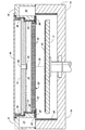
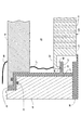
| JPS63187619A (ja) | 1987-01-30 | 1988-08-03 | Fuji Xerox Co Ltd | プラズマcvd装置 |
| US4854263B1 (en) * | 1987-08-14 | 1997-06-17 | Applied Materials Inc | Inlet manifold and methods for increasing gas dissociation and for PECVD of dielectric films |
| JPH02114530A (ja) * | 1988-10-25 | 1990-04-26 | Mitsubishi Electric Corp | 薄膜形成装置 |
| US5310453A (en) * | 1992-02-13 | 1994-05-10 | Tokyo Electron Yamanashi Limited | Plasma process method using an electrostatic chuck |
| JPH05299382A (ja) * | 1992-04-21 | 1993-11-12 | Mitsubishi Electric Corp | プラズマ処理装置およびその方法 |
| JP3155844B2 (ja) * | 1992-10-20 | 2001-04-16 | 日本真空技術株式会社 | 真空処理装置の高周波電極 |
| JP2662365B2 (ja) * | 1993-01-28 | 1997-10-08 | アプライド マテリアルズ インコーポレイテッド | 改良された排出システムを有する単一基板式の真空処理装置 |
| US5439524A (en) * | 1993-04-05 | 1995-08-08 | Vlsi Technology, Inc. | Plasma processing apparatus |
| US5350480A (en) * | 1993-07-23 | 1994-09-27 | Aspect International, Inc. | Surface cleaning and conditioning using hot neutral gas beam array |
| US5449410A (en) * | 1993-07-28 | 1995-09-12 | Applied Materials, Inc. | Plasma processing apparatus |
| US5647911A (en) * | 1993-12-14 | 1997-07-15 | Sony Corporation | Gas diffuser plate assembly and RF electrode |
| US5589002A (en) * | 1994-03-24 | 1996-12-31 | Applied Materials, Inc. | Gas distribution plate for semiconductor wafer processing apparatus with means for inhibiting arcing |
| US5628829A (en) * | 1994-06-03 | 1997-05-13 | Materials Research Corporation | Method and apparatus for low temperature deposition of CVD and PECVD films |
| US5665640A (en) * | 1994-06-03 | 1997-09-09 | Sony Corporation | Method for producing titanium-containing thin films by low temperature plasma-enhanced chemical vapor deposition using a rotating susceptor reactor |
| JP3360098B2 (ja) * | 1995-04-20 | 2002-12-24 | 東京エレクトロン株式会社 | 処理装置のシャワーヘッド構造 |
| US5569356A (en) * | 1995-05-19 | 1996-10-29 | Lam Research Corporation | Electrode clamping assembly and method for assembly and use thereof |
| US5997962A (en) * | 1995-06-30 | 1999-12-07 | Tokyo Electron Limited | Plasma process utilizing an electrostatic chuck |
| JPH09153481A (ja) * | 1995-11-30 | 1997-06-10 | Sumitomo Metal Ind Ltd | プラズマ処理装置 |
| TW335517B (en) * | 1996-03-01 | 1998-07-01 | Hitachi Ltd | Apparatus and method for processing plasma |
| US5741363A (en) * | 1996-03-22 | 1998-04-21 | Advanced Technology Materials, Inc. | Interiorly partitioned vapor injector for delivery of source reagent vapor mixtures for chemical vapor deposition |
| US5614026A (en) * | 1996-03-29 | 1997-03-25 | Lam Research Corporation | Showerhead for uniform distribution of process gas |
| US5844205A (en) * | 1996-04-19 | 1998-12-01 | Applied Komatsu Technology, Inc. | Heated substrate support structure |
| US5997642A (en) * | 1996-05-21 | 1999-12-07 | Symetrix Corporation | Method and apparatus for misted deposition of integrated circuit quality thin films |
| US5846332A (en) * | 1996-07-12 | 1998-12-08 | Applied Materials, Inc. | Thermally floating pedestal collar in a chemical vapor deposition chamber |
| US5882411A (en) * | 1996-10-21 | 1999-03-16 | Applied Materials, Inc. | Faceplate thermal choke in a CVD plasma reactor |
| US6114216A (en) * | 1996-11-13 | 2000-09-05 | Applied Materials, Inc. | Methods for shallow trench isolation |
| US5989652A (en) * | 1997-01-31 | 1999-11-23 | Tokyo Electron Limited | Method of low temperature plasma enhanced chemical vapor deposition of tin film over titanium for use in via level applications |
| US6093645A (en) * | 1997-02-10 | 2000-07-25 | Tokyo Electron Limited | Elimination of titanium nitride film deposition in tungsten plug technology using PE-CVD-TI and in-situ plasma nitridation |
| US5994678A (en) * | 1997-02-12 | 1999-11-30 | Applied Materials, Inc. | Apparatus for ceramic pedestal and metal shaft assembly |
| US6024799A (en) * | 1997-07-11 | 2000-02-15 | Applied Materials, Inc. | Chemical vapor deposition manifold |
| US5968276A (en) * | 1997-07-11 | 1999-10-19 | Applied Materials, Inc. | Heat exchange passage connection |
| JP3480271B2 (ja) * | 1997-10-07 | 2003-12-15 | 東京エレクトロン株式会社 | 熱処理装置のシャワーヘッド構造 |
| US6024044A (en) * | 1997-10-09 | 2000-02-15 | Applied Komatsu Technology, Inc. | Dual frequency excitation of plasma for film deposition |
| US6079356A (en) * | 1997-12-02 | 2000-06-27 | Applied Materials, Inc. | Reactor optimized for chemical vapor deposition of titanium |
| US6106625A (en) * | 1997-12-02 | 2000-08-22 | Applied Materials, Inc. | Reactor useful for chemical vapor deposition of titanium nitride |
| JP3725325B2 (ja) * | 1998-03-18 | 2005-12-07 | 株式会社日立製作所 | 半導体製造方法ならびに半導体製造装置 |
| US6129808A (en) * | 1998-03-31 | 2000-10-10 | Lam Research Corporation | Low contamination high density plasma etch chambers and methods for making the same |
| US5997649A (en) * | 1998-04-09 | 1999-12-07 | Tokyo Electron Limited | Stacked showerhead assembly for delivering gases and RF power to a reaction chamber |
| KR100267885B1 (ko) * | 1998-05-18 | 2000-11-01 | 서성기 | 반도체 박막증착장치 |
| US6050216A (en) * | 1998-08-21 | 2000-04-18 | M.E.C. Technology, Inc. | Showerhead electrode for plasma processing |
| US6302057B1 (en) * | 1998-09-15 | 2001-10-16 | Tokyo Electron Limited | Apparatus and method for electrically isolating an electrode in a PECVD process chamber |
| KR100745495B1 (ko) * | 1999-03-10 | 2007-08-03 | 동경 엘렉트론 주식회사 | 반도체 제조방법 및 반도체 제조장치 |
| WO2000063956A1 (en) * | 1999-04-20 | 2000-10-26 | Sony Corporation | Method and apparatus for thin-film deposition, and method of manufacturing thin-film semiconductor device |
| US6123775A (en) * | 1999-06-30 | 2000-09-26 | Lam Research Corporation | Reaction chamber component having improved temperature uniformity |
| US6254742B1 (en) * | 1999-07-12 | 2001-07-03 | Semitool, Inc. | Diffuser with spiral opening pattern for an electroplating reactor vessel |
| US6364949B1 (en) * | 1999-10-19 | 2002-04-02 | Applied Materials, Inc. | 300 mm CVD chamber design for metal-organic thin film deposition |
| US6673198B1 (en) * | 1999-12-22 | 2004-01-06 | Lam Research Corporation | Semiconductor processing equipment having improved process drift control |
| US6477980B1 (en) * | 2000-01-20 | 2002-11-12 | Applied Materials, Inc. | Flexibly suspended gas distribution manifold for plasma chamber |
| US6772827B2 (en) * | 2000-01-20 | 2004-08-10 | Applied Materials, Inc. | Suspended gas distribution manifold for plasma chamber |
| US6170432B1 (en) * | 2000-01-24 | 2001-01-09 | M.E.C. Technology, Inc. | Showerhead electrode assembly for plasma processing |
| JP3501715B2 (ja) * | 2000-03-21 | 2004-03-02 | シャープ株式会社 | プラズマプロセス装置 |
| US6857387B1 (en) * | 2000-05-03 | 2005-02-22 | Applied Materials, Inc. | Multiple frequency plasma chamber with grounding capacitor at cathode |
| US6461435B1 (en) * | 2000-06-22 | 2002-10-08 | Applied Materials, Inc. | Showerhead with reduced contact area |
| JP2002045683A (ja) * | 2000-08-08 | 2002-02-12 | Hitachi Kokusai Electric Inc | 基板処理装置 |
| JP4381588B2 (ja) * | 2000-10-25 | 2009-12-09 | ソニー株式会社 | 加熱を伴う処理装置 |
| JP2002261036A (ja) * | 2001-02-28 | 2002-09-13 | Dainippon Screen Mfg Co Ltd | 熱処理装置 |
| KR100377096B1 (ko) * | 2001-05-08 | 2003-03-26 | (주)넥소 | 개선된 샤워헤드를 구비한 반도체 제조장치 |
| US6827815B2 (en) * | 2002-01-15 | 2004-12-07 | Applied Materials, Inc. | Showerhead assembly for a processing chamber |
| US6838012B2 (en) * | 2002-10-31 | 2005-01-04 | Lam Research Corporation | Methods for etching dielectric materials |
| US7270713B2 (en) * | 2003-01-07 | 2007-09-18 | Applied Materials, Inc. | Tunable gas distribution plate assembly |
| US6942753B2 (en) * | 2003-04-16 | 2005-09-13 | Applied Materials, Inc. | Gas distribution plate assembly for large area plasma enhanced chemical vapor deposition |
| US7645341B2 (en) * | 2003-12-23 | 2010-01-12 | Lam Research Corporation | Showerhead electrode assembly for plasma processing apparatuses |
| US7429410B2 (en) * | 2004-09-20 | 2008-09-30 | Applied Materials, Inc. | Diffuser gravity support |
-
2005
- 2005-02-22 JP JP2005045994A patent/JP4698251B2/ja not_active Expired - Lifetime
- 2005-02-23 TW TW094105457A patent/TWI290962B/zh not_active IP Right Cessation
- 2005-02-23 US US11/063,454 patent/US7722925B2/en not_active Expired - Fee Related
- 2005-02-24 KR KR1020050015466A patent/KR100769963B1/ko not_active Expired - Lifetime
- 2005-02-24 CN CN201110128778.7A patent/CN102212798B/zh not_active Expired - Lifetime
- 2005-02-24 CN CN2005100716031A patent/CN1673410B/zh not_active Expired - Lifetime
-
2010
- 2010-12-14 JP JP2010278191A patent/JP5366923B2/ja not_active Expired - Lifetime
Cited By (1)
| Publication number | Priority date | Publication date | Assignee | Title |
|---|---|---|---|---|
| KR101529669B1 (ko) * | 2008-06-12 | 2015-06-18 | 주성엔지니어링(주) | 기판처리장치 |
Also Published As
| Publication number | Publication date |
|---|---|
| CN102212798B (zh) | 2015-01-21 |
| JP2005256172A (ja) | 2005-09-22 |
| US7722925B2 (en) | 2010-05-25 |
| JP2011089208A (ja) | 2011-05-06 |
| KR20060042164A (ko) | 2006-05-12 |
| CN102212798A (zh) | 2011-10-12 |
| US20050183827A1 (en) | 2005-08-25 |
| CN1673410A (zh) | 2005-09-28 |
| JP5366923B2 (ja) | 2013-12-11 |
| KR100769963B1 (ko) | 2007-10-25 |
| TW200533776A (en) | 2005-10-16 |
| CN1673410B (zh) | 2011-07-06 |
| TWI290962B (en) | 2007-12-11 |
Similar Documents
| Publication | Publication Date | Title |
|---|---|---|
| JP4698251B2 (ja) | 可動又は柔軟なシャワーヘッド取り付け | |
| KR100929455B1 (ko) | 플라즈마 챔버용의 현가형 가스 분배 매니폴드 | |
| EP1046729B1 (en) | CVD processing chamber | |
| US7083702B2 (en) | RF current return path for a large area substrate plasma reactor | |
| JP4430253B2 (ja) | ガス分配プレートを備えたチャンバ及び装置とガス分配プレートの熱応力を最小限にする方法 | |
| TWI355674B (en) | Showerhead assembly and apparatus for manufacturin | |
| US9580804B2 (en) | Diffuser support | |
| US20010047762A1 (en) | Processing apparatus | |
| US7641762B2 (en) | Gas sealing skirt for suspended showerhead in process chamber | |
| US20130087309A1 (en) | Substrate support with temperature control | |
| CN104377155B (zh) | 静电卡盘以及等离子体加工设备 | |
| CN200996043Y (zh) | 一种屏蔽框架组件 | |
| TW200302541A (en) | Heated vacuum support apparatus | |
| TWI738006B (zh) | 真空處理裝置、支持軸 |
Legal Events
| Date | Code | Title | Description |
|---|---|---|---|
| A521 | Request for written amendment filed |
Free format text: JAPANESE INTERMEDIATE CODE: A523 Effective date: 20051201 |
|
| A621 | Written request for application examination |
Free format text: JAPANESE INTERMEDIATE CODE: A621 Effective date: 20051201 |
|
| A521 | Request for written amendment filed |
Free format text: JAPANESE INTERMEDIATE CODE: A523 Effective date: 20051213 |
|
| A521 | Request for written amendment filed |
Free format text: JAPANESE INTERMEDIATE CODE: A523 Effective date: 20080307 |
|
| A131 | Notification of reasons for refusal |
Free format text: JAPANESE INTERMEDIATE CODE: A131 Effective date: 20081209 |
|
| A601 | Written request for extension of time |
Free format text: JAPANESE INTERMEDIATE CODE: A601 Effective date: 20090309 |
|
| A602 | Written permission of extension of time |
Free format text: JAPANESE INTERMEDIATE CODE: A602 Effective date: 20090312 |
|
| A521 | Request for written amendment filed |
Free format text: JAPANESE INTERMEDIATE CODE: A523 Effective date: 20090401 |
|
| A131 | Notification of reasons for refusal |
Free format text: JAPANESE INTERMEDIATE CODE: A131 Effective date: 20091020 |
|
| A601 | Written request for extension of time |
Free format text: JAPANESE INTERMEDIATE CODE: A601 Effective date: 20100120 |
|
| A602 | Written permission of extension of time |
Free format text: JAPANESE INTERMEDIATE CODE: A602 Effective date: 20100125 |
|
| A601 | Written request for extension of time |
Free format text: JAPANESE INTERMEDIATE CODE: A601 Effective date: 20100222 |
|
| A602 | Written permission of extension of time |
Free format text: JAPANESE INTERMEDIATE CODE: A602 Effective date: 20100225 |
|
| A601 | Written request for extension of time |
Free format text: JAPANESE INTERMEDIATE CODE: A601 Effective date: 20100323 |
|
| A602 | Written permission of extension of time |
Free format text: JAPANESE INTERMEDIATE CODE: A602 Effective date: 20100326 |
|
| A521 | Request for written amendment filed |
Free format text: JAPANESE INTERMEDIATE CODE: A523 Effective date: 20100415 |
|
| A131 | Notification of reasons for refusal |
Free format text: JAPANESE INTERMEDIATE CODE: A131 Effective date: 20100914 |
|
| RD03 | Notification of appointment of power of attorney |
Free format text: JAPANESE INTERMEDIATE CODE: A7423 Effective date: 20101130 |
|
| A521 | Request for written amendment filed |
Free format text: JAPANESE INTERMEDIATE CODE: A523 Effective date: 20101214 |
|
| TRDD | Decision of grant or rejection written | ||
| A01 | Written decision to grant a patent or to grant a registration (utility model) |
Free format text: JAPANESE INTERMEDIATE CODE: A01 Effective date: 20110201 |
|
| A61 | First payment of annual fees (during grant procedure) |
Free format text: JAPANESE INTERMEDIATE CODE: A61 Effective date: 20110301 |
|
| R150 | Certificate of patent or registration of utility model |
Ref document number: 4698251 Country of ref document: JP Free format text: JAPANESE INTERMEDIATE CODE: R150 |
|
| R250 | Receipt of annual fees |
Free format text: JAPANESE INTERMEDIATE CODE: R250 |
|
| R250 | Receipt of annual fees |
Free format text: JAPANESE INTERMEDIATE CODE: R250 |
|
| R250 | Receipt of annual fees |
Free format text: JAPANESE INTERMEDIATE CODE: R250 |
|
| R250 | Receipt of annual fees |
Free format text: JAPANESE INTERMEDIATE CODE: R250 |
|
| R250 | Receipt of annual fees |
Free format text: JAPANESE INTERMEDIATE CODE: R250 |
|
| R250 | Receipt of annual fees |
Free format text: JAPANESE INTERMEDIATE CODE: R250 |
|
| R250 | Receipt of annual fees |
Free format text: JAPANESE INTERMEDIATE CODE: R250 |
|
| R250 | Receipt of annual fees |
Free format text: JAPANESE INTERMEDIATE CODE: R250 |
|
| R250 | Receipt of annual fees |
Free format text: JAPANESE INTERMEDIATE CODE: R250 |
|
| R250 | Receipt of annual fees |
Free format text: JAPANESE INTERMEDIATE CODE: R250 |
|
| R250 | Receipt of annual fees |
Free format text: JAPANESE INTERMEDIATE CODE: R250 |
|
| EXPY | Cancellation because of completion of term |