JP3914239B2 - 配線基板および配線基板の製造方法 - Google Patents
配線基板および配線基板の製造方法 Download PDFInfo
- Publication number
- JP3914239B2 JP3914239B2 JP2005073946A JP2005073946A JP3914239B2 JP 3914239 B2 JP3914239 B2 JP 3914239B2 JP 2005073946 A JP2005073946 A JP 2005073946A JP 2005073946 A JP2005073946 A JP 2005073946A JP 3914239 B2 JP3914239 B2 JP 3914239B2
- Authority
- JP
- Japan
- Prior art keywords
- wiring
- semiconductor chip
- insulating layer
- wiring board
- pattern
- Prior art date
- Legal status (The legal status is an assumption and is not a legal conclusion. Google has not performed a legal analysis and makes no representation as to the accuracy of the status listed.)
- Expired - Fee Related
Links
Images


Classifications
-
- H—ELECTRICITY
- H05—ELECTRIC TECHNIQUES NOT OTHERWISE PROVIDED FOR
- H05K—PRINTED CIRCUITS; CASINGS OR CONSTRUCTIONAL DETAILS OF ELECTRIC APPARATUS; MANUFACTURE OF ASSEMBLAGES OF ELECTRICAL COMPONENTS
- H05K1/00—Printed circuits
- H05K1/18—Printed circuits structurally associated with non-printed electric components
-
- H—ELECTRICITY
- H01—ELECTRIC ELEMENTS
- H01L—SEMICONDUCTOR DEVICES NOT COVERED BY CLASS H10
- H01L23/00—Details of semiconductor or other solid state devices
- H01L23/52—Arrangements for conducting electric current within the device in operation from one component to another, i.e. interconnections, e.g. wires, lead frames
- H01L23/538—Arrangements for conducting electric current within the device in operation from one component to another, i.e. interconnections, e.g. wires, lead frames the interconnection structure between a plurality of semiconductor chips being formed on, or in, insulating substrates
- H01L23/5383—Multilayer substrates
-
- H—ELECTRICITY
- H01—ELECTRIC ELEMENTS
- H01L—SEMICONDUCTOR DEVICES NOT COVERED BY CLASS H10
- H01L21/00—Processes or apparatus adapted for the manufacture or treatment of semiconductor or solid state devices or of parts thereof
- H01L21/67—Apparatus specially adapted for handling semiconductor or electric solid state devices during manufacture or treatment thereof; Apparatus specially adapted for handling wafers during manufacture or treatment of semiconductor or electric solid state devices or components ; Apparatus not specifically provided for elsewhere
- H01L21/683—Apparatus specially adapted for handling semiconductor or electric solid state devices during manufacture or treatment thereof; Apparatus specially adapted for handling wafers during manufacture or treatment of semiconductor or electric solid state devices or components ; Apparatus not specifically provided for elsewhere for supporting or gripping
- H01L21/6835—Apparatus specially adapted for handling semiconductor or electric solid state devices during manufacture or treatment thereof; Apparatus specially adapted for handling wafers during manufacture or treatment of semiconductor or electric solid state devices or components ; Apparatus not specifically provided for elsewhere for supporting or gripping using temporarily an auxiliary support
-
- H—ELECTRICITY
- H01—ELECTRIC ELEMENTS
- H01L—SEMICONDUCTOR DEVICES NOT COVERED BY CLASS H10
- H01L23/00—Details of semiconductor or other solid state devices
- H01L23/16—Fillings or auxiliary members in containers or encapsulations, e.g. centering rings
- H01L23/18—Fillings characterised by the material, its physical or chemical properties, or its arrangement within the complete device
-
- H—ELECTRICITY
- H01—ELECTRIC ELEMENTS
- H01L—SEMICONDUCTOR DEVICES NOT COVERED BY CLASS H10
- H01L23/00—Details of semiconductor or other solid state devices
- H01L23/28—Encapsulations, e.g. encapsulating layers, coatings, e.g. for protection
- H01L23/31—Encapsulations, e.g. encapsulating layers, coatings, e.g. for protection characterised by the arrangement or shape
- H01L23/3107—Encapsulations, e.g. encapsulating layers, coatings, e.g. for protection characterised by the arrangement or shape the device being completely enclosed
- H01L23/3121—Encapsulations, e.g. encapsulating layers, coatings, e.g. for protection characterised by the arrangement or shape the device being completely enclosed a substrate forming part of the encapsulation
- H01L23/3128—Encapsulations, e.g. encapsulating layers, coatings, e.g. for protection characterised by the arrangement or shape the device being completely enclosed a substrate forming part of the encapsulation the substrate having spherical bumps for external connection
-
- H—ELECTRICITY
- H01—ELECTRIC ELEMENTS
- H01L—SEMICONDUCTOR DEVICES NOT COVERED BY CLASS H10
- H01L23/00—Details of semiconductor or other solid state devices
- H01L23/48—Arrangements for conducting electric current to or from the solid state body in operation, e.g. leads, terminal arrangements ; Selection of materials therefor
- H01L23/488—Arrangements for conducting electric current to or from the solid state body in operation, e.g. leads, terminal arrangements ; Selection of materials therefor consisting of soldered or bonded constructions
- H01L23/498—Leads, i.e. metallisations or lead-frames on insulating substrates, e.g. chip carriers
- H01L23/49805—Leads, i.e. metallisations or lead-frames on insulating substrates, e.g. chip carriers the leads being also applied on the sidewalls or the bottom of the substrate, e.g. leadless packages for surface mounting
-
- H—ELECTRICITY
- H01—ELECTRIC ELEMENTS
- H01L—SEMICONDUCTOR DEVICES NOT COVERED BY CLASS H10
- H01L23/00—Details of semiconductor or other solid state devices
- H01L23/52—Arrangements for conducting electric current within the device in operation from one component to another, i.e. interconnections, e.g. wires, lead frames
- H01L23/538—Arrangements for conducting electric current within the device in operation from one component to another, i.e. interconnections, e.g. wires, lead frames the interconnection structure between a plurality of semiconductor chips being formed on, or in, insulating substrates
- H01L23/5389—Arrangements for conducting electric current within the device in operation from one component to another, i.e. interconnections, e.g. wires, lead frames the interconnection structure between a plurality of semiconductor chips being formed on, or in, insulating substrates the chips being integrally enclosed by the interconnect and support structures
-
- H—ELECTRICITY
- H01—ELECTRIC ELEMENTS
- H01L—SEMICONDUCTOR DEVICES NOT COVERED BY CLASS H10
- H01L24/00—Arrangements for connecting or disconnecting semiconductor or solid-state bodies; Methods or apparatus related thereto
- H01L24/80—Methods for connecting semiconductor or other solid state bodies using means for bonding being attached to, or being formed on, the surface to be connected
- H01L24/81—Methods for connecting semiconductor or other solid state bodies using means for bonding being attached to, or being formed on, the surface to be connected using a bump connector
-
- H—ELECTRICITY
- H05—ELECTRIC TECHNIQUES NOT OTHERWISE PROVIDED FOR
- H05K—PRINTED CIRCUITS; CASINGS OR CONSTRUCTIONAL DETAILS OF ELECTRIC APPARATUS; MANUFACTURE OF ASSEMBLAGES OF ELECTRICAL COMPONENTS
- H05K3/00—Apparatus or processes for manufacturing printed circuits
- H05K3/22—Secondary treatment of printed circuits
-
- H—ELECTRICITY
- H01—ELECTRIC ELEMENTS
- H01L—SEMICONDUCTOR DEVICES NOT COVERED BY CLASS H10
- H01L21/00—Processes or apparatus adapted for the manufacture or treatment of semiconductor or solid state devices or of parts thereof
- H01L21/02—Manufacture or treatment of semiconductor devices or of parts thereof
- H01L21/04—Manufacture or treatment of semiconductor devices or of parts thereof the devices having at least one potential-jump barrier or surface barrier, e.g. PN junction, depletion layer or carrier concentration layer
- H01L21/50—Assembly of semiconductor devices using processes or apparatus not provided for in a single one of the subgroups H01L21/06 - H01L21/326, e.g. sealing of a cap to a base of a container
- H01L21/56—Encapsulations, e.g. encapsulation layers, coatings
- H01L21/563—Encapsulation of active face of flip-chip device, e.g. underfilling or underencapsulation of flip-chip, encapsulation preform on chip or mounting substrate
-
- H—ELECTRICITY
- H01—ELECTRIC ELEMENTS
- H01L—SEMICONDUCTOR DEVICES NOT COVERED BY CLASS H10
- H01L2221/00—Processes or apparatus adapted for the manufacture or treatment of semiconductor or solid state devices or of parts thereof covered by H01L21/00
- H01L2221/67—Apparatus for handling semiconductor or electric solid state devices during manufacture or treatment thereof; Apparatus for handling wafers during manufacture or treatment of semiconductor or electric solid state devices or components; Apparatus not specifically provided for elsewhere
- H01L2221/683—Apparatus for handling semiconductor or electric solid state devices during manufacture or treatment thereof; Apparatus for handling wafers during manufacture or treatment of semiconductor or electric solid state devices or components; Apparatus not specifically provided for elsewhere for supporting or gripping
- H01L2221/68304—Apparatus for handling semiconductor or electric solid state devices during manufacture or treatment thereof; Apparatus for handling wafers during manufacture or treatment of semiconductor or electric solid state devices or components; Apparatus not specifically provided for elsewhere for supporting or gripping using temporarily an auxiliary support
- H01L2221/68345—Apparatus for handling semiconductor or electric solid state devices during manufacture or treatment thereof; Apparatus for handling wafers during manufacture or treatment of semiconductor or electric solid state devices or components; Apparatus not specifically provided for elsewhere for supporting or gripping using temporarily an auxiliary support used as a support during the manufacture of self supporting substrates
-
- H—ELECTRICITY
- H01—ELECTRIC ELEMENTS
- H01L—SEMICONDUCTOR DEVICES NOT COVERED BY CLASS H10
- H01L2224/00—Indexing scheme for arrangements for connecting or disconnecting semiconductor or solid-state bodies and methods related thereto as covered by H01L24/00
- H01L2224/01—Means for bonding being attached to, or being formed on, the surface to be connected, e.g. chip-to-package, die-attach, "first-level" interconnects; Manufacturing methods related thereto
- H01L2224/10—Bump connectors; Manufacturing methods related thereto
- H01L2224/11—Manufacturing methods
- H01L2224/113—Manufacturing methods by local deposition of the material of the bump connector
- H01L2224/1133—Manufacturing methods by local deposition of the material of the bump connector in solid form
- H01L2224/1134—Stud bumping, i.e. using a wire-bonding apparatus
-
- H—ELECTRICITY
- H01—ELECTRIC ELEMENTS
- H01L—SEMICONDUCTOR DEVICES NOT COVERED BY CLASS H10
- H01L2224/00—Indexing scheme for arrangements for connecting or disconnecting semiconductor or solid-state bodies and methods related thereto as covered by H01L24/00
- H01L2224/01—Means for bonding being attached to, or being formed on, the surface to be connected, e.g. chip-to-package, die-attach, "first-level" interconnects; Manufacturing methods related thereto
- H01L2224/10—Bump connectors; Manufacturing methods related thereto
- H01L2224/12—Structure, shape, material or disposition of the bump connectors prior to the connecting process
- H01L2224/13—Structure, shape, material or disposition of the bump connectors prior to the connecting process of an individual bump connector
- H01L2224/13001—Core members of the bump connector
- H01L2224/13099—Material
- H01L2224/131—Material with a principal constituent of the material being a metal or a metalloid, e.g. boron [B], silicon [Si], germanium [Ge], arsenic [As], antimony [Sb], tellurium [Te] and polonium [Po], and alloys thereof
- H01L2224/13138—Material with a principal constituent of the material being a metal or a metalloid, e.g. boron [B], silicon [Si], germanium [Ge], arsenic [As], antimony [Sb], tellurium [Te] and polonium [Po], and alloys thereof the principal constituent melting at a temperature of greater than or equal to 950°C and less than 1550°C
- H01L2224/13144—Gold [Au] as principal constituent
-
- H—ELECTRICITY
- H01—ELECTRIC ELEMENTS
- H01L—SEMICONDUCTOR DEVICES NOT COVERED BY CLASS H10
- H01L2224/00—Indexing scheme for arrangements for connecting or disconnecting semiconductor or solid-state bodies and methods related thereto as covered by H01L24/00
- H01L2224/01—Means for bonding being attached to, or being formed on, the surface to be connected, e.g. chip-to-package, die-attach, "first-level" interconnects; Manufacturing methods related thereto
- H01L2224/10—Bump connectors; Manufacturing methods related thereto
- H01L2224/12—Structure, shape, material or disposition of the bump connectors prior to the connecting process
- H01L2224/13—Structure, shape, material or disposition of the bump connectors prior to the connecting process of an individual bump connector
- H01L2224/1354—Coating
- H01L2224/13599—Material
- H01L2224/136—Material with a principal constituent of the material being a metal or a metalloid, e.g. boron [B], silicon [Si], germanium [Ge], arsenic [As], antimony [Sb], tellurium [Te] and polonium [Po], and alloys thereof
-
- H—ELECTRICITY
- H01—ELECTRIC ELEMENTS
- H01L—SEMICONDUCTOR DEVICES NOT COVERED BY CLASS H10
- H01L2224/00—Indexing scheme for arrangements for connecting or disconnecting semiconductor or solid-state bodies and methods related thereto as covered by H01L24/00
- H01L2224/01—Means for bonding being attached to, or being formed on, the surface to be connected, e.g. chip-to-package, die-attach, "first-level" interconnects; Manufacturing methods related thereto
- H01L2224/10—Bump connectors; Manufacturing methods related thereto
- H01L2224/15—Structure, shape, material or disposition of the bump connectors after the connecting process
- H01L2224/16—Structure, shape, material or disposition of the bump connectors after the connecting process of an individual bump connector
- H01L2224/161—Disposition
- H01L2224/16151—Disposition the bump connector connecting between a semiconductor or solid-state body and an item not being a semiconductor or solid-state body, e.g. chip-to-substrate, chip-to-passive
- H01L2224/16221—Disposition the bump connector connecting between a semiconductor or solid-state body and an item not being a semiconductor or solid-state body, e.g. chip-to-substrate, chip-to-passive the body and the item being stacked
- H01L2224/16225—Disposition the bump connector connecting between a semiconductor or solid-state body and an item not being a semiconductor or solid-state body, e.g. chip-to-substrate, chip-to-passive the body and the item being stacked the item being non-metallic, e.g. insulating substrate with or without metallisation
-
- H—ELECTRICITY
- H01—ELECTRIC ELEMENTS
- H01L—SEMICONDUCTOR DEVICES NOT COVERED BY CLASS H10
- H01L2224/00—Indexing scheme for arrangements for connecting or disconnecting semiconductor or solid-state bodies and methods related thereto as covered by H01L24/00
- H01L2224/01—Means for bonding being attached to, or being formed on, the surface to be connected, e.g. chip-to-package, die-attach, "first-level" interconnects; Manufacturing methods related thereto
- H01L2224/26—Layer connectors, e.g. plate connectors, solder or adhesive layers; Manufacturing methods related thereto
- H01L2224/31—Structure, shape, material or disposition of the layer connectors after the connecting process
- H01L2224/32—Structure, shape, material or disposition of the layer connectors after the connecting process of an individual layer connector
- H01L2224/321—Disposition
- H01L2224/32151—Disposition the layer connector connecting between a semiconductor or solid-state body and an item not being a semiconductor or solid-state body, e.g. chip-to-substrate, chip-to-passive
- H01L2224/32221—Disposition the layer connector connecting between a semiconductor or solid-state body and an item not being a semiconductor or solid-state body, e.g. chip-to-substrate, chip-to-passive the body and the item being stacked
- H01L2224/32225—Disposition the layer connector connecting between a semiconductor or solid-state body and an item not being a semiconductor or solid-state body, e.g. chip-to-substrate, chip-to-passive the body and the item being stacked the item being non-metallic, e.g. insulating substrate with or without metallisation
-
- H—ELECTRICITY
- H01—ELECTRIC ELEMENTS
- H01L—SEMICONDUCTOR DEVICES NOT COVERED BY CLASS H10
- H01L2224/00—Indexing scheme for arrangements for connecting or disconnecting semiconductor or solid-state bodies and methods related thereto as covered by H01L24/00
- H01L2224/73—Means for bonding being of different types provided for in two or more of groups H01L2224/10, H01L2224/18, H01L2224/26, H01L2224/34, H01L2224/42, H01L2224/50, H01L2224/63, H01L2224/71
- H01L2224/732—Location after the connecting process
- H01L2224/73201—Location after the connecting process on the same surface
- H01L2224/73203—Bump and layer connectors
- H01L2224/73204—Bump and layer connectors the bump connector being embedded into the layer connector
-
- H—ELECTRICITY
- H01—ELECTRIC ELEMENTS
- H01L—SEMICONDUCTOR DEVICES NOT COVERED BY CLASS H10
- H01L2224/00—Indexing scheme for arrangements for connecting or disconnecting semiconductor or solid-state bodies and methods related thereto as covered by H01L24/00
- H01L2224/80—Methods for connecting semiconductor or other solid state bodies using means for bonding being attached to, or being formed on, the surface to be connected
- H01L2224/81—Methods for connecting semiconductor or other solid state bodies using means for bonding being attached to, or being formed on, the surface to be connected using a bump connector
- H01L2224/81001—Methods for connecting semiconductor or other solid state bodies using means for bonding being attached to, or being formed on, the surface to be connected using a bump connector involving a temporary auxiliary member not forming part of the bonding apparatus
- H01L2224/81005—Methods for connecting semiconductor or other solid state bodies using means for bonding being attached to, or being formed on, the surface to be connected using a bump connector involving a temporary auxiliary member not forming part of the bonding apparatus being a temporary or sacrificial substrate
-
- H—ELECTRICITY
- H01—ELECTRIC ELEMENTS
- H01L—SEMICONDUCTOR DEVICES NOT COVERED BY CLASS H10
- H01L2224/00—Indexing scheme for arrangements for connecting or disconnecting semiconductor or solid-state bodies and methods related thereto as covered by H01L24/00
- H01L2224/80—Methods for connecting semiconductor or other solid state bodies using means for bonding being attached to, or being formed on, the surface to be connected
- H01L2224/81—Methods for connecting semiconductor or other solid state bodies using means for bonding being attached to, or being formed on, the surface to be connected using a bump connector
- H01L2224/8119—Arrangement of the bump connectors prior to mounting
- H01L2224/81191—Arrangement of the bump connectors prior to mounting wherein the bump connectors are disposed only on the semiconductor or solid-state body
-
- H—ELECTRICITY
- H01—ELECTRIC ELEMENTS
- H01L—SEMICONDUCTOR DEVICES NOT COVERED BY CLASS H10
- H01L2224/00—Indexing scheme for arrangements for connecting or disconnecting semiconductor or solid-state bodies and methods related thereto as covered by H01L24/00
- H01L2224/80—Methods for connecting semiconductor or other solid state bodies using means for bonding being attached to, or being formed on, the surface to be connected
- H01L2224/81—Methods for connecting semiconductor or other solid state bodies using means for bonding being attached to, or being formed on, the surface to be connected using a bump connector
- H01L2224/812—Applying energy for connecting
- H01L2224/8121—Applying energy for connecting using a reflow oven
-
- H—ELECTRICITY
- H01—ELECTRIC ELEMENTS
- H01L—SEMICONDUCTOR DEVICES NOT COVERED BY CLASS H10
- H01L2224/00—Indexing scheme for arrangements for connecting or disconnecting semiconductor or solid-state bodies and methods related thereto as covered by H01L24/00
- H01L2224/80—Methods for connecting semiconductor or other solid state bodies using means for bonding being attached to, or being formed on, the surface to be connected
- H01L2224/81—Methods for connecting semiconductor or other solid state bodies using means for bonding being attached to, or being formed on, the surface to be connected using a bump connector
- H01L2224/818—Bonding techniques
- H01L2224/81801—Soldering or alloying
- H01L2224/81815—Reflow soldering
-
- H—ELECTRICITY
- H01—ELECTRIC ELEMENTS
- H01L—SEMICONDUCTOR DEVICES NOT COVERED BY CLASS H10
- H01L2224/00—Indexing scheme for arrangements for connecting or disconnecting semiconductor or solid-state bodies and methods related thereto as covered by H01L24/00
- H01L2224/80—Methods for connecting semiconductor or other solid state bodies using means for bonding being attached to, or being formed on, the surface to be connected
- H01L2224/83—Methods for connecting semiconductor or other solid state bodies using means for bonding being attached to, or being formed on, the surface to be connected using a layer connector
- H01L2224/831—Methods for connecting semiconductor or other solid state bodies using means for bonding being attached to, or being formed on, the surface to be connected using a layer connector the layer connector being supplied to the parts to be connected in the bonding apparatus
- H01L2224/83102—Methods for connecting semiconductor or other solid state bodies using means for bonding being attached to, or being formed on, the surface to be connected using a layer connector the layer connector being supplied to the parts to be connected in the bonding apparatus using surface energy, e.g. capillary forces
-
- H—ELECTRICITY
- H01—ELECTRIC ELEMENTS
- H01L—SEMICONDUCTOR DEVICES NOT COVERED BY CLASS H10
- H01L2224/00—Indexing scheme for arrangements for connecting or disconnecting semiconductor or solid-state bodies and methods related thereto as covered by H01L24/00
- H01L2224/91—Methods for connecting semiconductor or solid state bodies including different methods provided for in two or more of groups H01L2224/80 - H01L2224/90
- H01L2224/92—Specific sequence of method steps
- H01L2224/921—Connecting a surface with connectors of different types
- H01L2224/9212—Sequential connecting processes
- H01L2224/92122—Sequential connecting processes the first connecting process involving a bump connector
- H01L2224/92125—Sequential connecting processes the first connecting process involving a bump connector the second connecting process involving a layer connector
-
- H—ELECTRICITY
- H01—ELECTRIC ELEMENTS
- H01L—SEMICONDUCTOR DEVICES NOT COVERED BY CLASS H10
- H01L23/00—Details of semiconductor or other solid state devices
- H01L23/48—Arrangements for conducting electric current to or from the solid state body in operation, e.g. leads, terminal arrangements ; Selection of materials therefor
- H01L23/488—Arrangements for conducting electric current to or from the solid state body in operation, e.g. leads, terminal arrangements ; Selection of materials therefor consisting of soldered or bonded constructions
- H01L23/498—Leads, i.e. metallisations or lead-frames on insulating substrates, e.g. chip carriers
- H01L23/49811—Additional leads joined to the metallisation on the insulating substrate, e.g. pins, bumps, wires, flat leads
- H01L23/49816—Spherical bumps on the substrate for external connection, e.g. ball grid arrays [BGA]
-
- H—ELECTRICITY
- H01—ELECTRIC ELEMENTS
- H01L—SEMICONDUCTOR DEVICES NOT COVERED BY CLASS H10
- H01L25/00—Assemblies consisting of a plurality of individual semiconductor or other solid state devices ; Multistep manufacturing processes thereof
- H01L25/03—Assemblies consisting of a plurality of individual semiconductor or other solid state devices ; Multistep manufacturing processes thereof all the devices being of a type provided for in the same subgroup of groups H01L27/00 - H01L33/00, or in a single subclass of H10K, H10N, e.g. assemblies of rectifier diodes
- H01L25/04—Assemblies consisting of a plurality of individual semiconductor or other solid state devices ; Multistep manufacturing processes thereof all the devices being of a type provided for in the same subgroup of groups H01L27/00 - H01L33/00, or in a single subclass of H10K, H10N, e.g. assemblies of rectifier diodes the devices not having separate containers
- H01L25/065—Assemblies consisting of a plurality of individual semiconductor or other solid state devices ; Multistep manufacturing processes thereof all the devices being of a type provided for in the same subgroup of groups H01L27/00 - H01L33/00, or in a single subclass of H10K, H10N, e.g. assemblies of rectifier diodes the devices not having separate containers the devices being of a type provided for in group H01L27/00
- H01L25/0655—Assemblies consisting of a plurality of individual semiconductor or other solid state devices ; Multistep manufacturing processes thereof all the devices being of a type provided for in the same subgroup of groups H01L27/00 - H01L33/00, or in a single subclass of H10K, H10N, e.g. assemblies of rectifier diodes the devices not having separate containers the devices being of a type provided for in group H01L27/00 the devices being arranged next to each other
-
- H—ELECTRICITY
- H01—ELECTRIC ELEMENTS
- H01L—SEMICONDUCTOR DEVICES NOT COVERED BY CLASS H10
- H01L2924/00—Indexing scheme for arrangements or methods for connecting or disconnecting semiconductor or solid-state bodies as covered by H01L24/00
- H01L2924/0001—Technical content checked by a classifier
- H01L2924/00011—Not relevant to the scope of the group, the symbol of which is combined with the symbol of this group
-
- H—ELECTRICITY
- H01—ELECTRIC ELEMENTS
- H01L—SEMICONDUCTOR DEVICES NOT COVERED BY CLASS H10
- H01L2924/00—Indexing scheme for arrangements or methods for connecting or disconnecting semiconductor or solid-state bodies as covered by H01L24/00
- H01L2924/0001—Technical content checked by a classifier
- H01L2924/00013—Fully indexed content
-
- H—ELECTRICITY
- H01—ELECTRIC ELEMENTS
- H01L—SEMICONDUCTOR DEVICES NOT COVERED BY CLASS H10
- H01L2924/00—Indexing scheme for arrangements or methods for connecting or disconnecting semiconductor or solid-state bodies as covered by H01L24/00
- H01L2924/0001—Technical content checked by a classifier
- H01L2924/00014—Technical content checked by a classifier the subject-matter covered by the group, the symbol of which is combined with the symbol of this group, being disclosed without further technical details
-
- H—ELECTRICITY
- H01—ELECTRIC ELEMENTS
- H01L—SEMICONDUCTOR DEVICES NOT COVERED BY CLASS H10
- H01L2924/00—Indexing scheme for arrangements or methods for connecting or disconnecting semiconductor or solid-state bodies as covered by H01L24/00
- H01L2924/01—Chemical elements
- H01L2924/01006—Carbon [C]
-
- H—ELECTRICITY
- H01—ELECTRIC ELEMENTS
- H01L—SEMICONDUCTOR DEVICES NOT COVERED BY CLASS H10
- H01L2924/00—Indexing scheme for arrangements or methods for connecting or disconnecting semiconductor or solid-state bodies as covered by H01L24/00
- H01L2924/01—Chemical elements
- H01L2924/01013—Aluminum [Al]
-
- H—ELECTRICITY
- H01—ELECTRIC ELEMENTS
- H01L—SEMICONDUCTOR DEVICES NOT COVERED BY CLASS H10
- H01L2924/00—Indexing scheme for arrangements or methods for connecting or disconnecting semiconductor or solid-state bodies as covered by H01L24/00
- H01L2924/01—Chemical elements
- H01L2924/01019—Potassium [K]
-
- H—ELECTRICITY
- H01—ELECTRIC ELEMENTS
- H01L—SEMICONDUCTOR DEVICES NOT COVERED BY CLASS H10
- H01L2924/00—Indexing scheme for arrangements or methods for connecting or disconnecting semiconductor or solid-state bodies as covered by H01L24/00
- H01L2924/01—Chemical elements
- H01L2924/01029—Copper [Cu]
-
- H—ELECTRICITY
- H01—ELECTRIC ELEMENTS
- H01L—SEMICONDUCTOR DEVICES NOT COVERED BY CLASS H10
- H01L2924/00—Indexing scheme for arrangements or methods for connecting or disconnecting semiconductor or solid-state bodies as covered by H01L24/00
- H01L2924/01—Chemical elements
- H01L2924/01033—Arsenic [As]
-
- H—ELECTRICITY
- H01—ELECTRIC ELEMENTS
- H01L—SEMICONDUCTOR DEVICES NOT COVERED BY CLASS H10
- H01L2924/00—Indexing scheme for arrangements or methods for connecting or disconnecting semiconductor or solid-state bodies as covered by H01L24/00
- H01L2924/01—Chemical elements
- H01L2924/0105—Tin [Sn]
-
- H—ELECTRICITY
- H01—ELECTRIC ELEMENTS
- H01L—SEMICONDUCTOR DEVICES NOT COVERED BY CLASS H10
- H01L2924/00—Indexing scheme for arrangements or methods for connecting or disconnecting semiconductor or solid-state bodies as covered by H01L24/00
- H01L2924/01—Chemical elements
- H01L2924/01078—Platinum [Pt]
-
- H—ELECTRICITY
- H01—ELECTRIC ELEMENTS
- H01L—SEMICONDUCTOR DEVICES NOT COVERED BY CLASS H10
- H01L2924/00—Indexing scheme for arrangements or methods for connecting or disconnecting semiconductor or solid-state bodies as covered by H01L24/00
- H01L2924/01—Chemical elements
- H01L2924/01079—Gold [Au]
-
- H—ELECTRICITY
- H01—ELECTRIC ELEMENTS
- H01L—SEMICONDUCTOR DEVICES NOT COVERED BY CLASS H10
- H01L2924/00—Indexing scheme for arrangements or methods for connecting or disconnecting semiconductor or solid-state bodies as covered by H01L24/00
- H01L2924/01—Chemical elements
- H01L2924/01082—Lead [Pb]
-
- H—ELECTRICITY
- H01—ELECTRIC ELEMENTS
- H01L—SEMICONDUCTOR DEVICES NOT COVERED BY CLASS H10
- H01L2924/00—Indexing scheme for arrangements or methods for connecting or disconnecting semiconductor or solid-state bodies as covered by H01L24/00
- H01L2924/013—Alloys
- H01L2924/014—Solder alloys
-
- H—ELECTRICITY
- H01—ELECTRIC ELEMENTS
- H01L—SEMICONDUCTOR DEVICES NOT COVERED BY CLASS H10
- H01L2924/00—Indexing scheme for arrangements or methods for connecting or disconnecting semiconductor or solid-state bodies as covered by H01L24/00
- H01L2924/10—Details of semiconductor or other solid state devices to be connected
- H01L2924/11—Device type
- H01L2924/12—Passive devices, e.g. 2 terminal devices
- H01L2924/1204—Optical Diode
- H01L2924/12042—LASER
-
- H—ELECTRICITY
- H01—ELECTRIC ELEMENTS
- H01L—SEMICONDUCTOR DEVICES NOT COVERED BY CLASS H10
- H01L2924/00—Indexing scheme for arrangements or methods for connecting or disconnecting semiconductor or solid-state bodies as covered by H01L24/00
- H01L2924/15—Details of package parts other than the semiconductor or other solid state devices to be connected
- H01L2924/151—Die mounting substrate
- H01L2924/1517—Multilayer substrate
- H01L2924/15192—Resurf arrangement of the internal vias
-
- H—ELECTRICITY
- H01—ELECTRIC ELEMENTS
- H01L—SEMICONDUCTOR DEVICES NOT COVERED BY CLASS H10
- H01L2924/00—Indexing scheme for arrangements or methods for connecting or disconnecting semiconductor or solid-state bodies as covered by H01L24/00
- H01L2924/15—Details of package parts other than the semiconductor or other solid state devices to be connected
- H01L2924/151—Die mounting substrate
- H01L2924/153—Connection portion
- H01L2924/1531—Connection portion the connection portion being formed only on the surface of the substrate opposite to the die mounting surface
- H01L2924/15311—Connection portion the connection portion being formed only on the surface of the substrate opposite to the die mounting surface being a ball array, e.g. BGA
-
- H—ELECTRICITY
- H01—ELECTRIC ELEMENTS
- H01L—SEMICONDUCTOR DEVICES NOT COVERED BY CLASS H10
- H01L2924/00—Indexing scheme for arrangements or methods for connecting or disconnecting semiconductor or solid-state bodies as covered by H01L24/00
- H01L2924/15—Details of package parts other than the semiconductor or other solid state devices to be connected
- H01L2924/151—Die mounting substrate
- H01L2924/153—Connection portion
- H01L2924/1532—Connection portion the connection portion being formed on the die mounting surface of the substrate
- H01L2924/1533—Connection portion the connection portion being formed on the die mounting surface of the substrate the connection portion being formed both on the die mounting surface of the substrate and outside the die mounting surface of the substrate
- H01L2924/15331—Connection portion the connection portion being formed on the die mounting surface of the substrate the connection portion being formed both on the die mounting surface of the substrate and outside the die mounting surface of the substrate being a ball array, e.g. BGA
-
- H—ELECTRICITY
- H01—ELECTRIC ELEMENTS
- H01L—SEMICONDUCTOR DEVICES NOT COVERED BY CLASS H10
- H01L2924/00—Indexing scheme for arrangements or methods for connecting or disconnecting semiconductor or solid-state bodies as covered by H01L24/00
- H01L2924/30—Technical effects
- H01L2924/35—Mechanical effects
- H01L2924/351—Thermal stress
- H01L2924/3511—Warping
-
- H—ELECTRICITY
- H01—ELECTRIC ELEMENTS
- H01L—SEMICONDUCTOR DEVICES NOT COVERED BY CLASS H10
- H01L2924/00—Indexing scheme for arrangements or methods for connecting or disconnecting semiconductor or solid-state bodies as covered by H01L24/00
- H01L2924/30—Technical effects
- H01L2924/38—Effects and problems related to the device integration
- H01L2924/381—Pitch distance
-
- H—ELECTRICITY
- H05—ELECTRIC TECHNIQUES NOT OTHERWISE PROVIDED FOR
- H05K—PRINTED CIRCUITS; CASINGS OR CONSTRUCTIONAL DETAILS OF ELECTRIC APPARATUS; MANUFACTURE OF ASSEMBLAGES OF ELECTRICAL COMPONENTS
- H05K1/00—Printed circuits
- H05K1/18—Printed circuits structurally associated with non-printed electric components
- H05K1/182—Printed circuits structurally associated with non-printed electric components associated with components mounted in the printed circuit board, e.g. insert mounted components [IMC]
- H05K1/185—Components encapsulated in the insulating substrate of the printed circuit or incorporated in internal layers of a multilayer circuit
-
- H—ELECTRICITY
- H05—ELECTRIC TECHNIQUES NOT OTHERWISE PROVIDED FOR
- H05K—PRINTED CIRCUITS; CASINGS OR CONSTRUCTIONAL DETAILS OF ELECTRIC APPARATUS; MANUFACTURE OF ASSEMBLAGES OF ELECTRICAL COMPONENTS
- H05K3/00—Apparatus or processes for manufacturing printed circuits
- H05K3/46—Manufacturing multilayer circuits
- H05K3/4644—Manufacturing multilayer circuits by building the multilayer layer by layer, i.e. build-up multilayer circuits
-
- Y—GENERAL TAGGING OF NEW TECHNOLOGICAL DEVELOPMENTS; GENERAL TAGGING OF CROSS-SECTIONAL TECHNOLOGIES SPANNING OVER SEVERAL SECTIONS OF THE IPC; TECHNICAL SUBJECTS COVERED BY FORMER USPC CROSS-REFERENCE ART COLLECTIONS [XRACs] AND DIGESTS
- Y10—TECHNICAL SUBJECTS COVERED BY FORMER USPC
- Y10T—TECHNICAL SUBJECTS COVERED BY FORMER US CLASSIFICATION
- Y10T29/00—Metal working
- Y10T29/49—Method of mechanical manufacture
- Y10T29/49002—Electrical device making
- Y10T29/49117—Conductor or circuit manufacturing
- Y10T29/49124—On flat or curved insulated base, e.g., printed circuit, etc.
- Y10T29/49126—Assembling bases
-
- Y—GENERAL TAGGING OF NEW TECHNOLOGICAL DEVELOPMENTS; GENERAL TAGGING OF CROSS-SECTIONAL TECHNOLOGIES SPANNING OVER SEVERAL SECTIONS OF THE IPC; TECHNICAL SUBJECTS COVERED BY FORMER USPC CROSS-REFERENCE ART COLLECTIONS [XRACs] AND DIGESTS
- Y10—TECHNICAL SUBJECTS COVERED BY FORMER USPC
- Y10T—TECHNICAL SUBJECTS COVERED BY FORMER US CLASSIFICATION
- Y10T29/00—Metal working
- Y10T29/49—Method of mechanical manufacture
- Y10T29/49002—Electrical device making
- Y10T29/49117—Conductor or circuit manufacturing
- Y10T29/49124—On flat or curved insulated base, e.g., printed circuit, etc.
- Y10T29/4913—Assembling to base an electrical component, e.g., capacitor, etc.
- Y10T29/49133—Assembling to base an electrical component, e.g., capacitor, etc. with component orienting
- Y10T29/49135—Assembling to base an electrical component, e.g., capacitor, etc. with component orienting and shaping, e.g., cutting or bending, etc.
-
- Y—GENERAL TAGGING OF NEW TECHNOLOGICAL DEVELOPMENTS; GENERAL TAGGING OF CROSS-SECTIONAL TECHNOLOGIES SPANNING OVER SEVERAL SECTIONS OF THE IPC; TECHNICAL SUBJECTS COVERED BY FORMER USPC CROSS-REFERENCE ART COLLECTIONS [XRACs] AND DIGESTS
- Y10—TECHNICAL SUBJECTS COVERED BY FORMER USPC
- Y10T—TECHNICAL SUBJECTS COVERED BY FORMER US CLASSIFICATION
- Y10T29/00—Metal working
- Y10T29/49—Method of mechanical manufacture
- Y10T29/49002—Electrical device making
- Y10T29/49117—Conductor or circuit manufacturing
- Y10T29/49124—On flat or curved insulated base, e.g., printed circuit, etc.
- Y10T29/49155—Manufacturing circuit on or in base
- Y10T29/49156—Manufacturing circuit on or in base with selective destruction of conductive paths
Description
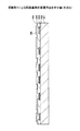
101 コア基板
102,119,202,219 端子接続部
103,111,113,203 絶縁層
104,115 シード層
105,116,205,216,217,222 ビアプラグ
106,117,206,217,223,225 パターン配線
107,207 接続部
108,208 スタッドバンプ
109,209 半導体チップ
110,210 アンダーフィル
114 ビアホール
118,120,218,220 ソルダーレジスト層
121,221 ハンダバンプ
Claims (11)
- 半導体チップが内蔵された配線基板であって、
前記半導体チップが埋設される絶縁層と、
前記半導体チップの第1の側に形成され、該半導体チップに接続されるとともに第1の端子接続部に接続される第1のパターン配線と、
前記半導体チップの第2の側に形成され、該半導体チップに接続されるとともに第2の端子接続部に接続される第2のパターン配線と、
前記絶縁層に形成され、前記第1のパターン配線と前記第2のパターン配線を接続するビアプラグと、
前記絶縁層に形成される補強構造体と、を有し、
前記絶縁層は、前記第1のパターン配線および前記半導体チップを覆う絶縁層と、該絶縁層上に形成される別の絶縁層を含むように構成され、
前記補強構造体は、前記第1のパターン配線および前記半導体チップを覆う絶縁層上に設置されるとともに、前記別の絶縁層に埋設されていることを特徴とする配線基板。 - 前記補強構造体は、前記半導体チップと同一平面上に形成されることを特徴とする請求項1記載の配線基板。
- 前記補強構造体は、前記半導体チップを囲むように形成されることを特徴とする請求項1または2記載の配線基板。
- 前記第1の配線パターン、前記第2の配線パターン、および前記ビアプラグは、多層配線構造を構成することを特徴とする請求項1乃至3のうち、いずれか1項記載の配線基板。
- 前記補強構造体は、有機コア材料または金属材料よりなることを特徴とする請求項1乃至4のうち、いずれか1項記載の配線基板。
- 半導体チップが内蔵された配線基板の製造方法であって、
前記半導体チップに接続される第1のパターン配線と、該第1のパターン配線に接続される第1の端子接続部とを形成する工程と、
前記第1のパターン配線上に前記半導体チップを設置する工程と、
前記第1のパターン配線と前記半導体チップを覆う絶縁層を形成する工程と、
前記絶縁層上に補強構造体を設置する工程と、
前記絶縁層上に、前記補強構造体を埋設する別の絶縁層を形成する工程と、
前記絶縁層および前記別の絶縁層に、前記第1のパターン配線に接続されるビアプラグを形成する工程と、
前記ビアプラグに接続される第2のパターン配線と、該第2のパターン配線に接続される第2の端子接続部を形成する工程と、を有することを特徴とする配線基板の製造方法。 - 前記補強構造体は、前記半導体チップと同一平面上に設置されることを特徴とする請求項6記載の配線基板の製造方法。
- 前記第1のパターン配線は、コア基板上に形成され、当該コア基板を除去する工程をさらに有することを特徴とする請求項6または7記載の配線基板の製造方法。
- 前記コア基板は導電性の材料よりなり、前記第1の端子接続部は当該コア基板を電極にした電解メッキにより形成される部分を含むことを特徴とする請求項8記載の配線基板の製造方法。
- 前記半導体チップにはスタッドバンプが設置されており、当該スタッドバンプを介して当該半導体チップが前記第1のパターン配線に電気的に接続されることを特徴とする請求項6乃至9のうち、いずれか1項記載の配線基板の製造方法。
- 前記スタッドバンプと前記第1のパターン配線の間には、半田よりなる接続部が形成されていることを特徴とする請求項10記載の配線基板の製造方法。
Priority Applications (6)
| Application Number | Priority Date | Filing Date | Title |
|---|---|---|---|
| JP2005073946A JP3914239B2 (ja) | 2005-03-15 | 2005-03-15 | 配線基板および配線基板の製造方法 |
| US11/372,916 US7884484B2 (en) | 2005-03-15 | 2006-03-10 | Wiring board and method of manufacturing the same |
| KR1020060023432A KR20060101286A (ko) | 2005-03-15 | 2006-03-14 | 배선 기판과 그 제조 방법 |
| TW095108709A TWI394503B (zh) | 2005-03-15 | 2006-03-15 | 佈線板及其製造方法 |
| EP06005295A EP1703558A3 (en) | 2005-03-15 | 2006-03-15 | Wiring board with embedded semiconductor chip, embedded reinforcing member and method of manufacturing the same |
| CN2006100598487A CN1835654B (zh) | 2005-03-15 | 2006-03-15 | 配线基板及其制造方法 |
Applications Claiming Priority (1)
| Application Number | Priority Date | Filing Date | Title |
|---|---|---|---|
| JP2005073946A JP3914239B2 (ja) | 2005-03-15 | 2005-03-15 | 配線基板および配線基板の製造方法 |
Publications (2)
| Publication Number | Publication Date |
|---|---|
| JP2006261246A JP2006261246A (ja) | 2006-09-28 |
| JP3914239B2 true JP3914239B2 (ja) | 2007-05-16 |
Family
ID=36581823
Family Applications (1)
| Application Number | Title | Priority Date | Filing Date |
|---|---|---|---|
| JP2005073946A Expired - Fee Related JP3914239B2 (ja) | 2005-03-15 | 2005-03-15 | 配線基板および配線基板の製造方法 |
Country Status (6)
| Country | Link |
|---|---|
| US (1) | US7884484B2 (ja) |
| EP (1) | EP1703558A3 (ja) |
| JP (1) | JP3914239B2 (ja) |
| KR (1) | KR20060101286A (ja) |
| CN (1) | CN1835654B (ja) |
| TW (1) | TWI394503B (ja) |
Families Citing this family (60)
| Publication number | Priority date | Publication date | Assignee | Title |
|---|---|---|---|---|
| JP4526983B2 (ja) | 2005-03-15 | 2010-08-18 | 新光電気工業株式会社 | 配線基板の製造方法 |
| JP2008084959A (ja) | 2006-09-26 | 2008-04-10 | Shinko Electric Ind Co Ltd | 半導体装置及びその製造方法 |
| JP4906462B2 (ja) * | 2006-10-11 | 2012-03-28 | 新光電気工業株式会社 | 電子部品内蔵基板および電子部品内蔵基板の製造方法 |
| JP2008235550A (ja) * | 2007-03-20 | 2008-10-02 | Mitsubishi Electric Corp | プリント配線板、プリント配線板の製造方法、及びそれを用いた電子機器 |
| US7498198B2 (en) * | 2007-04-30 | 2009-03-03 | International Business Machines Corporation | Structure and method for stress reduction in flip chip microelectronic packages using underfill materials with spatially varying properties |
| US20080284047A1 (en) * | 2007-05-15 | 2008-11-20 | Eric Tosaya | Chip Package with Stiffener Ring |
| DE102007022959B4 (de) * | 2007-05-16 | 2012-04-19 | Infineon Technologies Ag | Verfahren zur Herstellung von Halbleitervorrichtungen |
| US7863088B2 (en) * | 2007-05-16 | 2011-01-04 | Infineon Technologies Ag | Semiconductor device including covering a semiconductor with a molding compound and forming a through hole in the molding compound |
| JP4518114B2 (ja) * | 2007-07-25 | 2010-08-04 | Tdk株式会社 | 電子部品内蔵基板及びその製造方法 |
| JP4518113B2 (ja) * | 2007-07-25 | 2010-08-04 | Tdk株式会社 | 電子部品内蔵基板及びその製造方法 |
| JP5025399B2 (ja) * | 2007-09-27 | 2012-09-12 | 新光電気工業株式会社 | 配線基板及びその製造方法 |
| US7790576B2 (en) * | 2007-11-29 | 2010-09-07 | Stats Chippac, Ltd. | Semiconductor device and method of forming through hole vias in die extension region around periphery of die |
| US20090170241A1 (en) * | 2007-12-26 | 2009-07-02 | Stats Chippac, Ltd. | Semiconductor Device and Method of Forming the Device Using Sacrificial Carrier |
| US8008133B2 (en) * | 2008-02-11 | 2011-08-30 | Globalfoundries Inc. | Chip package with channel stiffener frame |
| TWI356479B (en) * | 2008-03-04 | 2012-01-11 | Advanced Semiconductor Eng | Package structure with embedded die and method of |
| US8313984B2 (en) * | 2008-03-19 | 2012-11-20 | Ati Technologies Ulc | Die substrate with reinforcement structure |
| JP2010010644A (ja) * | 2008-05-27 | 2010-01-14 | Toshiba Corp | 半導体装置の製造方法 |
| KR100965339B1 (ko) * | 2008-06-04 | 2010-06-22 | 삼성전기주식회사 | 전자부품 내장형 인쇄회로기판 및 그 제조방법 |
| JP2009302427A (ja) * | 2008-06-17 | 2009-12-24 | Shinko Electric Ind Co Ltd | 半導体装置および半導体装置の製造方法 |
| US7888184B2 (en) * | 2008-06-20 | 2011-02-15 | Stats Chippac Ltd. | Integrated circuit packaging system with embedded circuitry and post, and method of manufacture thereof |
| JP2010021423A (ja) * | 2008-07-11 | 2010-01-28 | Tdk Corp | Ic内蔵基板及びその製造方法 |
| US7923850B2 (en) * | 2008-08-26 | 2011-04-12 | Advanced Micro Devices, Inc. | Semiconductor chip with solder joint protection ring |
| JP5505307B2 (ja) * | 2008-10-06 | 2014-05-28 | 日本電気株式会社 | 機能素子内蔵基板及びその製造方法、並びに電子機器 |
| TWI458400B (zh) * | 2008-10-31 | 2014-10-21 | Taiyo Yuden Kk | Printed circuit board and manufacturing method thereof |
| US8354304B2 (en) * | 2008-12-05 | 2013-01-15 | Stats Chippac, Ltd. | Semiconductor device and method of forming conductive posts embedded in photosensitive encapsulant |
| JP4924955B2 (ja) * | 2009-01-30 | 2012-04-25 | Tdk株式会社 | 電子部品内蔵基板、その製造方法、及びその検査方法 |
| JP5477372B2 (ja) * | 2009-03-11 | 2014-04-23 | 日本電気株式会社 | 機能素子内蔵基板、及びその製造方法、並びに電子機器 |
| US8026608B2 (en) * | 2009-03-24 | 2011-09-27 | General Electric Company | Stackable electronic package |
| US8216887B2 (en) * | 2009-05-04 | 2012-07-10 | Advanced Micro Devices, Inc. | Semiconductor chip package with stiffener frame and configured lid |
| JPWO2011016555A1 (ja) | 2009-08-07 | 2013-01-17 | 日本電気株式会社 | 半導体装置とその製造方法 |
| US8410376B2 (en) * | 2009-08-28 | 2013-04-02 | Ibiden Co., Ltd. | Printed wiring board and method for manufacturing the same |
| DE102009029201B4 (de) | 2009-09-04 | 2019-05-09 | Robert Bosch Gmbh | Verfahren zur Herstellung eines ein mikro- oder nanostrukuriertes Bauelement umfassenden Bauteils |
| US8796561B1 (en) * | 2009-10-05 | 2014-08-05 | Amkor Technology, Inc. | Fan out build up substrate stackable package and method |
| US20110100692A1 (en) * | 2009-11-02 | 2011-05-05 | Roden Topacio | Circuit Board with Variable Topography Solder Interconnects |
| US8937381B1 (en) | 2009-12-03 | 2015-01-20 | Amkor Technology, Inc. | Thin stackable package and method |
| JPWO2011089936A1 (ja) | 2010-01-22 | 2013-05-23 | 日本電気株式会社 | 機能素子内蔵基板及び配線基板 |
| WO2011118572A1 (ja) | 2010-03-23 | 2011-09-29 | 日本電気株式会社 | 半導体装置の製造方法 |
| US8338231B2 (en) * | 2010-03-29 | 2012-12-25 | Infineon Technologies Ag | Encapsulated semiconductor chip with external contact pads and manufacturing method thereof |
| US8232138B2 (en) | 2010-04-14 | 2012-07-31 | Advanced Micro Devices, Inc. | Circuit board with notched stiffener frame |
| US9735113B2 (en) * | 2010-05-24 | 2017-08-15 | STATS ChipPAC Pte. Ltd. | Semiconductor device and method of forming ultra thin multi-die face-to-face WLCSP |
| US8105872B2 (en) * | 2010-06-02 | 2012-01-31 | Stats Chippac, Ltd. | Semiconductor device and method of forming prefabricated EMI shielding frame with cavities containing penetrable material over semiconductor die |
| US8097490B1 (en) | 2010-08-27 | 2012-01-17 | Stats Chippac, Ltd. | Semiconductor device and method of forming stepped interconnect layer for stacked semiconductor die |
| JP2012069734A (ja) * | 2010-09-24 | 2012-04-05 | Toshiba Corp | 半導体装置の製造方法 |
| US8976529B2 (en) * | 2011-01-14 | 2015-03-10 | Taiwan Semiconductor Manufacturing Company, Ltd. | Lid design for reliability enhancement in flip chip package |
| AT13055U1 (de) * | 2011-01-26 | 2013-05-15 | Austria Tech & System Tech | Verfahren zur integration eines elektronischen bauteils in eine leiterplatte oder ein leiterplatten-zwischenprodukt sowie leiterplatte oder leiterplatten-zwischenprodukt |
| JP5540276B2 (ja) * | 2011-03-31 | 2014-07-02 | Tdk株式会社 | 電子部品内蔵基板及びその製造方法 |
| US20130105975A1 (en) * | 2011-10-26 | 2013-05-02 | Rafiqul Hussain | Semiconductor chip device with thermal interface material frame |
| CN103779290B (zh) * | 2012-10-26 | 2016-12-21 | 碁鼎科技秦皇岛有限公司 | 连接基板及层叠封装结构 |
| US9867282B2 (en) | 2013-08-16 | 2018-01-09 | Ati Technologies Ulc | Circuit board with corner hollows |
| TWI514530B (zh) * | 2013-08-28 | 2015-12-21 | Via Tech Inc | 線路基板、半導體封裝結構及線路基板製程 |
| JP6761224B2 (ja) * | 2014-02-19 | 2020-09-23 | 味の素株式会社 | プリント配線板、半導体装置及び樹脂シートセット |
| FR3018953B1 (fr) | 2014-03-19 | 2017-09-15 | St Microelectronics Crolles 2 Sas | Puce de circuit integre montee sur un interposeur |
| JP6358431B2 (ja) * | 2014-08-25 | 2018-07-18 | 新光電気工業株式会社 | 電子部品装置及びその製造方法 |
| TWI582861B (zh) * | 2014-09-12 | 2017-05-11 | 矽品精密工業股份有限公司 | 嵌埋元件之封裝結構及其製法 |
| KR102412612B1 (ko) | 2015-08-28 | 2022-06-23 | 삼성전자주식회사 | 패키지 기판 및 프리프레그 |
| KR101787832B1 (ko) * | 2015-10-22 | 2017-10-19 | 앰코 테크놀로지 코리아 주식회사 | 반도체 패키지 제조 방법 및 이를 이용한 반도체 패키지 |
| US9853011B2 (en) | 2016-03-29 | 2017-12-26 | Advanced Semiconductor Engineering, Inc. | Semiconductor package structure and method for manufacturing the same |
| US10629519B2 (en) * | 2016-11-29 | 2020-04-21 | Advanced Semiconductor Engineering, Inc. | Semiconductor device package and method of manufacturing the same |
| DE102018200597A1 (de) * | 2018-01-15 | 2019-07-18 | Siemens Healthcare Gmbh | Trägersubstrat für eine Röntgendetektoranordnung, Röntgendetektoranordnung und Röntgengerät |
| US11848280B2 (en) * | 2020-11-25 | 2023-12-19 | ADVANCED SEMlCONDUCTOR ENGINEERING, INC. | Method for manufacturing assembly structure by using frame structure on substrate |
Family Cites Families (25)
| Publication number | Priority date | Publication date | Assignee | Title |
|---|---|---|---|---|
| JPS60116191A (ja) | 1983-11-29 | 1985-06-22 | イビデン株式会社 | 電子部品搭載用基板の製造方法 |
| JPH0566973U (ja) * | 1992-02-04 | 1993-09-03 | 株式会社富士通ゼネラル | バンプ形成構造 |
| SG76530A1 (en) | 1997-03-03 | 2000-11-21 | Hitachi Chemical Co Ltd | Circuit boards using heat resistant resin for adhesive layers |
| JP3481444B2 (ja) | 1998-01-14 | 2003-12-22 | シャープ株式会社 | 半導体装置及びその製造方法 |
| JP2001015638A (ja) | 1999-06-30 | 2001-01-19 | Mitsumi Electric Co Ltd | Icパッケージの基板 |
| JP4251421B2 (ja) | 2000-01-13 | 2009-04-08 | 新光電気工業株式会社 | 半導体装置の製造方法 |
| US6348728B1 (en) | 2000-01-28 | 2002-02-19 | Fujitsu Limited | Semiconductor device having a plurality of semiconductor elements interconnected by a redistribution layer |
| EP1259103B1 (en) * | 2000-02-25 | 2007-05-30 | Ibiden Co., Ltd. | Multilayer printed wiring board and method for producing multilayer printed wiring board |
| CN1498417A (zh) | 2000-09-19 | 2004-05-19 | 纳诺皮尔斯技术公司 | 用于在无线频率识别装置中装配元件和天线的方法 |
| JP2002100696A (ja) | 2000-09-20 | 2002-04-05 | Hitachi Cable Ltd | 半導体装置及びその製造方法 |
| TW511415B (en) | 2001-01-19 | 2002-11-21 | Matsushita Electric Ind Co Ltd | Component built-in module and its manufacturing method |
| JP4248761B2 (ja) * | 2001-04-27 | 2009-04-02 | 新光電気工業株式会社 | 半導体パッケージ及びその製造方法並びに半導体装置 |
| US6903278B2 (en) | 2001-06-29 | 2005-06-07 | Intel Corporation | Arrangements to provide mechanical stiffening elements to a thin-core or coreless substrate |
| TW550997B (en) | 2001-10-18 | 2003-09-01 | Matsushita Electric Ind Co Ltd | Module with built-in components and the manufacturing method thereof |
| JP3591524B2 (ja) | 2002-05-27 | 2004-11-24 | 日本電気株式会社 | 半導体装置搭載基板とその製造方法およびその基板検査法、並びに半導体パッケージ |
| US7474538B2 (en) * | 2002-05-27 | 2009-01-06 | Nec Corporation | Semiconductor device mounting board, method of manufacturing the same, method of inspecting the same, and semiconductor package |
| JP2003347741A (ja) | 2002-05-30 | 2003-12-05 | Taiyo Yuden Co Ltd | 複合多層基板およびそれを用いたモジュール |
| FI20030293A (fi) | 2003-02-26 | 2004-08-27 | Imbera Electronics Oy | Menetelmä elektroniikkamoduulin valmistamiseksi ja elektroniikkamoduuli |
| JP4346333B2 (ja) * | 2003-03-26 | 2009-10-21 | 新光電気工業株式会社 | 半導体素子を内蔵した多層回路基板の製造方法 |
| JP2004335641A (ja) * | 2003-05-06 | 2004-11-25 | Canon Inc | 半導体素子内蔵基板の製造方法 |
| US6928726B2 (en) * | 2003-07-24 | 2005-08-16 | Motorola, Inc. | Circuit board with embedded components and method of manufacture |
| US6864165B1 (en) | 2003-09-15 | 2005-03-08 | International Business Machines Corporation | Method of fabricating integrated electronic chip with an interconnect device |
| DE102004022884B4 (de) | 2004-05-06 | 2007-07-19 | Infineon Technologies Ag | Halbleiterbauteil mit einem Umverdrahtungssubstrat und Verfahren zur Herstellung desselben |
| TWI245388B (en) * | 2005-01-06 | 2005-12-11 | Phoenix Prec Technology Corp | Three dimensional package structure of semiconductor chip embedded in substrate and method for fabricating the same |
| JP4526983B2 (ja) | 2005-03-15 | 2010-08-18 | 新光電気工業株式会社 | 配線基板の製造方法 |
-
2005
- 2005-03-15 JP JP2005073946A patent/JP3914239B2/ja not_active Expired - Fee Related
-
2006
- 2006-03-10 US US11/372,916 patent/US7884484B2/en not_active Expired - Fee Related
- 2006-03-14 KR KR1020060023432A patent/KR20060101286A/ko not_active Application Discontinuation
- 2006-03-15 CN CN2006100598487A patent/CN1835654B/zh not_active Expired - Fee Related
- 2006-03-15 TW TW095108709A patent/TWI394503B/zh not_active IP Right Cessation
- 2006-03-15 EP EP06005295A patent/EP1703558A3/en not_active Withdrawn
Also Published As
| Publication number | Publication date |
|---|---|
| EP1703558A2 (en) | 2006-09-20 |
| KR20060101286A (ko) | 2006-09-22 |
| CN1835654A (zh) | 2006-09-20 |
| TWI394503B (zh) | 2013-04-21 |
| EP1703558A3 (en) | 2010-01-20 |
| TW200640326A (en) | 2006-11-16 |
| CN1835654B (zh) | 2011-06-29 |
| US20060208356A1 (en) | 2006-09-21 |
| JP2006261246A (ja) | 2006-09-28 |
| US7884484B2 (en) | 2011-02-08 |
Similar Documents
| Publication | Publication Date | Title |
|---|---|---|
| JP3914239B2 (ja) | 配線基板および配線基板の製造方法 | |
| JP6298722B2 (ja) | 配線基板、半導体装置及び配線基板の製造方法 | |
| JP4016039B2 (ja) | 配線基板および配線基板の製造方法 | |
| JP6375121B2 (ja) | 配線基板、半導体装置及び配線基板の製造方法 | |
| US8987901B2 (en) | Component built-in wiring board and manufacturing method of component built-in wiring board | |
| JP4575071B2 (ja) | 電子部品内蔵基板の製造方法 | |
| JP4526983B2 (ja) | 配線基板の製造方法 | |
| JP5662551B1 (ja) | 配線基板、半導体装置及び配線基板の製造方法 | |
| JP6661232B2 (ja) | 配線基板、半導体装置、配線基板の製造方法及び半導体装置の製造方法 | |
| JP2010267948A (ja) | コアレス・パッケージ基板およびその製造方法 | |
| JP2008300507A (ja) | 配線基板とその製造方法 | |
| US9392684B2 (en) | Wiring substrate and method for manufacturing wiring substrate | |
| US11430725B2 (en) | Wiring board and method of manufacturing the same | |
| JP2009081356A (ja) | 配線基板の製造方法及び配線基板 | |
| JP5221887B2 (ja) | 配線基盤の製造方法 | |
| JP2008124247A (ja) | 部品内蔵基板及びその製造方法 | |
| JP2010226075A (ja) | 配線板及びその製造方法 | |
| JP2009267149A (ja) | 部品内蔵配線板、部品内蔵配線板の製造方法 | |
| JP2007311492A (ja) | 半導体装置の製造方法 | |
| JP6626687B2 (ja) | 配線基板、半導体装置及び配線基板の製造方法 | |
| JP2006049762A (ja) | 部品内蔵基板及び部品内蔵基板の製造方法 | |
| JP4580752B2 (ja) | 半導体装置の製造方法 | |
| KR20150111682A (ko) | 인쇄회로기판 및 그 제조방법 | |
| JP5511922B2 (ja) | 配線基板とその製造方法 | |
| KR20130028583A (ko) | 회로기판의 제조방법 및 회로기판 |
Legal Events
| Date | Code | Title | Description |
|---|---|---|---|
| A621 | Written request for application examination |
Free format text: JAPANESE INTERMEDIATE CODE: A621 Effective date: 20060821 |
|
| A871 | Explanation of circumstances concerning accelerated examination |
Free format text: JAPANESE INTERMEDIATE CODE: A871 Effective date: 20060821 |
|
| A975 | Report on accelerated examination |
Free format text: JAPANESE INTERMEDIATE CODE: A971005 Effective date: 20061018 |
|
| A131 | Notification of reasons for refusal |
Free format text: JAPANESE INTERMEDIATE CODE: A131 Effective date: 20061024 |
|
| A521 | Written amendment |
Free format text: JAPANESE INTERMEDIATE CODE: A523 Effective date: 20061221 |
|
| TRDD | Decision of grant or rejection written | ||
| A01 | Written decision to grant a patent or to grant a registration (utility model) |
Free format text: JAPANESE INTERMEDIATE CODE: A01 Effective date: 20070130 |
|
| A61 | First payment of annual fees (during grant procedure) |
Free format text: JAPANESE INTERMEDIATE CODE: A61 Effective date: 20070201 |
|
| R150 | Certificate of patent or registration of utility model |
Ref document number: 3914239 Country of ref document: JP Free format text: JAPANESE INTERMEDIATE CODE: R150 Free format text: JAPANESE INTERMEDIATE CODE: R150 |
|
| FPAY | Renewal fee payment (event date is renewal date of database) |
Free format text: PAYMENT UNTIL: 20110209 Year of fee payment: 4 |
|
| FPAY | Renewal fee payment (event date is renewal date of database) |
Free format text: PAYMENT UNTIL: 20110209 Year of fee payment: 4 |
|
| FPAY | Renewal fee payment (event date is renewal date of database) |
Free format text: PAYMENT UNTIL: 20120209 Year of fee payment: 5 |
|
| FPAY | Renewal fee payment (event date is renewal date of database) |
Free format text: PAYMENT UNTIL: 20120209 Year of fee payment: 5 |
|
| FPAY | Renewal fee payment (event date is renewal date of database) |
Free format text: PAYMENT UNTIL: 20130209 Year of fee payment: 6 |
|
| FPAY | Renewal fee payment (event date is renewal date of database) |
Free format text: PAYMENT UNTIL: 20140209 Year of fee payment: 7 |
|
| LAPS | Cancellation because of no payment of annual fees |