JP2014075581A - 表示装置および電子機器 - Google Patents
表示装置および電子機器 Download PDFInfo
- Publication number
- JP2014075581A JP2014075581A JP2013187215A JP2013187215A JP2014075581A JP 2014075581 A JP2014075581 A JP 2014075581A JP 2013187215 A JP2013187215 A JP 2013187215A JP 2013187215 A JP2013187215 A JP 2013187215A JP 2014075581 A JP2014075581 A JP 2014075581A
- Authority
- JP
- Japan
- Prior art keywords
- oxide layer
- insulating film
- film
- display device
- oxide
- Prior art date
- Legal status (The legal status is an assumption and is not a legal conclusion. Google has not performed a legal analysis and makes no representation as to the accuracy of the status listed.)
- Withdrawn
Links
- 239000004065 semiconductor Substances 0.000 claims abstract description 133
- 230000015572 biosynthetic process Effects 0.000 claims abstract description 50
- 239000003990 capacitor Substances 0.000 claims description 134
- 238000000034 method Methods 0.000 claims description 57
- XUIMIQQOPSSXEZ-UHFFFAOYSA-N Silicon Chemical compound [Si] XUIMIQQOPSSXEZ-UHFFFAOYSA-N 0.000 claims description 24
- 229910052710 silicon Inorganic materials 0.000 claims description 24
- 239000010703 silicon Substances 0.000 claims description 24
- 230000008569 process Effects 0.000 claims description 21
- 229910052782 aluminium Inorganic materials 0.000 claims description 16
- XAGFODPZIPBFFR-UHFFFAOYSA-N aluminium Chemical compound [Al] XAGFODPZIPBFFR-UHFFFAOYSA-N 0.000 claims description 16
- 239000010936 titanium Substances 0.000 claims description 13
- RTAQQCXQSZGOHL-UHFFFAOYSA-N Titanium Chemical compound [Ti] RTAQQCXQSZGOHL-UHFFFAOYSA-N 0.000 claims description 11
- 229910052719 titanium Inorganic materials 0.000 claims description 11
- 229910052733 gallium Inorganic materials 0.000 claims description 10
- GYHNNYVSQQEPJS-UHFFFAOYSA-N Gallium Chemical compound [Ga] GYHNNYVSQQEPJS-UHFFFAOYSA-N 0.000 claims description 7
- ATJFFYVFTNAWJD-UHFFFAOYSA-N Tin Chemical compound [Sn] ATJFFYVFTNAWJD-UHFFFAOYSA-N 0.000 claims description 7
- 229910052727 yttrium Inorganic materials 0.000 claims description 7
- VWQVUPCCIRVNHF-UHFFFAOYSA-N yttrium atom Chemical compound [Y] VWQVUPCCIRVNHF-UHFFFAOYSA-N 0.000 claims description 7
- 229910052684 Cerium Inorganic materials 0.000 claims description 6
- QCWXUUIWCKQGHC-UHFFFAOYSA-N Zirconium Chemical compound [Zr] QCWXUUIWCKQGHC-UHFFFAOYSA-N 0.000 claims description 6
- 229910052732 germanium Inorganic materials 0.000 claims description 6
- GNPVGFCGXDBREM-UHFFFAOYSA-N germanium atom Chemical compound [Ge] GNPVGFCGXDBREM-UHFFFAOYSA-N 0.000 claims description 6
- 229910052735 hafnium Inorganic materials 0.000 claims description 6
- VBJZVLUMGGDVMO-UHFFFAOYSA-N hafnium atom Chemical compound [Hf] VBJZVLUMGGDVMO-UHFFFAOYSA-N 0.000 claims description 6
- 229910052746 lanthanum Inorganic materials 0.000 claims description 6
- FZLIPJUXYLNCLC-UHFFFAOYSA-N lanthanum atom Chemical compound [La] FZLIPJUXYLNCLC-UHFFFAOYSA-N 0.000 claims description 6
- 229910052718 tin Inorganic materials 0.000 claims description 6
- 229910052726 zirconium Inorganic materials 0.000 claims description 6
- TWNQGVIAIRXVLR-UHFFFAOYSA-N oxo(oxoalumanyloxy)alumane Chemical compound O=[Al]O[Al]=O TWNQGVIAIRXVLR-UHFFFAOYSA-N 0.000 claims description 5
- GWXLDORMOJMVQZ-UHFFFAOYSA-N cerium Chemical compound [Ce] GWXLDORMOJMVQZ-UHFFFAOYSA-N 0.000 claims 2
- 239000000758 substrate Substances 0.000 abstract description 78
- 238000004519 manufacturing process Methods 0.000 abstract description 24
- 239000010410 layer Substances 0.000 description 241
- 229910052760 oxygen Inorganic materials 0.000 description 69
- 239000001301 oxygen Substances 0.000 description 69
- QVGXLLKOCUKJST-UHFFFAOYSA-N atomic oxygen Chemical compound [O] QVGXLLKOCUKJST-UHFFFAOYSA-N 0.000 description 68
- IJGRMHOSHXDMSA-UHFFFAOYSA-N Atomic nitrogen Chemical compound N#N IJGRMHOSHXDMSA-UHFFFAOYSA-N 0.000 description 60
- 239000004973 liquid crystal related substance Substances 0.000 description 56
- 239000011701 zinc Substances 0.000 description 56
- 239000013078 crystal Substances 0.000 description 45
- 230000006870 function Effects 0.000 description 39
- 239000007789 gas Substances 0.000 description 36
- 229910052757 nitrogen Inorganic materials 0.000 description 30
- 239000000463 material Substances 0.000 description 29
- 239000001257 hydrogen Substances 0.000 description 26
- 229910052739 hydrogen Inorganic materials 0.000 description 26
- 238000010438 heat treatment Methods 0.000 description 24
- 238000012545 processing Methods 0.000 description 21
- UFHFLCQGNIYNRP-UHFFFAOYSA-N Hydrogen Chemical compound [H][H] UFHFLCQGNIYNRP-UHFFFAOYSA-N 0.000 description 19
- 229910052581 Si3N4 Inorganic materials 0.000 description 19
- HQVNEWCFYHHQES-UHFFFAOYSA-N silicon nitride Chemical compound N12[Si]34N5[Si]62N3[Si]51N64 HQVNEWCFYHHQES-UHFFFAOYSA-N 0.000 description 19
- 239000012535 impurity Substances 0.000 description 18
- 125000004429 atom Chemical group 0.000 description 16
- 230000005684 electric field Effects 0.000 description 16
- 238000000151 deposition Methods 0.000 description 15
- 229910052751 metal Inorganic materials 0.000 description 15
- QGZKDVFQNNGYKY-UHFFFAOYSA-N Ammonia Chemical compound N QGZKDVFQNNGYKY-UHFFFAOYSA-N 0.000 description 14
- 230000008021 deposition Effects 0.000 description 14
- 239000002184 metal Substances 0.000 description 14
- 239000000565 sealant Substances 0.000 description 13
- XLYOFNOQVPJJNP-UHFFFAOYSA-N water Substances O XLYOFNOQVPJJNP-UHFFFAOYSA-N 0.000 description 13
- 229910001868 water Inorganic materials 0.000 description 13
- 150000004767 nitrides Chemical class 0.000 description 11
- XLOMVQKBTHCTTD-UHFFFAOYSA-N Zinc monoxide Chemical compound [Zn]=O XLOMVQKBTHCTTD-UHFFFAOYSA-N 0.000 description 10
- 230000007547 defect Effects 0.000 description 10
- 239000010949 copper Substances 0.000 description 9
- 238000005530 etching Methods 0.000 description 9
- 239000000203 mixture Substances 0.000 description 9
- 238000004544 sputter deposition Methods 0.000 description 9
- RYGMFSIKBFXOCR-UHFFFAOYSA-N Copper Chemical compound [Cu] RYGMFSIKBFXOCR-UHFFFAOYSA-N 0.000 description 8
- 229910052802 copper Inorganic materials 0.000 description 8
- 238000003795 desorption Methods 0.000 description 8
- 150000002431 hydrogen Chemical class 0.000 description 8
- 239000002245 particle Substances 0.000 description 8
- VYPSYNLAJGMNEJ-UHFFFAOYSA-N Silicium dioxide Chemical compound O=[Si]=O VYPSYNLAJGMNEJ-UHFFFAOYSA-N 0.000 description 7
- 229910021529 ammonia Inorganic materials 0.000 description 7
- 239000000843 powder Substances 0.000 description 7
- 239000011347 resin Substances 0.000 description 7
- 229920005989 resin Polymers 0.000 description 7
- 239000002585 base Substances 0.000 description 6
- 230000005669 field effect Effects 0.000 description 6
- 230000004048 modification Effects 0.000 description 6
- 238000012986 modification Methods 0.000 description 6
- 230000003287 optical effect Effects 0.000 description 6
- 229910052814 silicon oxide Inorganic materials 0.000 description 6
- WFKWXMTUELFFGS-UHFFFAOYSA-N tungsten Chemical compound [W] WFKWXMTUELFFGS-UHFFFAOYSA-N 0.000 description 6
- 229910052721 tungsten Inorganic materials 0.000 description 6
- 239000010937 tungsten Substances 0.000 description 6
- HEZMWWAKWCSUCB-PHDIDXHHSA-N (3R,4R)-3,4-dihydroxycyclohexa-1,5-diene-1-carboxylic acid Chemical compound O[C@@H]1C=CC(C(O)=O)=C[C@H]1O HEZMWWAKWCSUCB-PHDIDXHHSA-N 0.000 description 5
- 229910021417 amorphous silicon Inorganic materials 0.000 description 5
- 238000004458 analytical method Methods 0.000 description 5
- 239000000969 carrier Substances 0.000 description 5
- 230000008859 change Effects 0.000 description 5
- 238000010586 diagram Methods 0.000 description 5
- 230000005012 migration Effects 0.000 description 5
- 238000013508 migration Methods 0.000 description 5
- 238000001004 secondary ion mass spectrometry Methods 0.000 description 5
- 239000011787 zinc oxide Substances 0.000 description 5
- XKRFYHLGVUSROY-UHFFFAOYSA-N Argon Chemical compound [Ar] XKRFYHLGVUSROY-UHFFFAOYSA-N 0.000 description 4
- 229910052783 alkali metal Inorganic materials 0.000 description 4
- 150000001340 alkali metals Chemical class 0.000 description 4
- 230000004888 barrier function Effects 0.000 description 4
- 230000005540 biological transmission Effects 0.000 description 4
- ZMIGMASIKSOYAM-UHFFFAOYSA-N cerium Chemical compound [Ce][Ce][Ce][Ce][Ce][Ce][Ce][Ce][Ce][Ce][Ce][Ce][Ce][Ce][Ce][Ce][Ce][Ce][Ce][Ce][Ce][Ce][Ce][Ce][Ce][Ce][Ce][Ce][Ce][Ce][Ce][Ce][Ce][Ce][Ce][Ce][Ce][Ce] ZMIGMASIKSOYAM-UHFFFAOYSA-N 0.000 description 4
- 238000005229 chemical vapour deposition Methods 0.000 description 4
- 238000004891 communication Methods 0.000 description 4
- 238000009792 diffusion process Methods 0.000 description 4
- AJNVQOSZGJRYEI-UHFFFAOYSA-N digallium;oxygen(2-) Chemical compound [O-2].[O-2].[O-2].[Ga+3].[Ga+3] AJNVQOSZGJRYEI-UHFFFAOYSA-N 0.000 description 4
- 238000005401 electroluminescence Methods 0.000 description 4
- 229910001195 gallium oxide Inorganic materials 0.000 description 4
- 239000011521 glass Substances 0.000 description 4
- 238000012905 input function Methods 0.000 description 4
- 229910044991 metal oxide Inorganic materials 0.000 description 4
- 150000004706 metal oxides Chemical class 0.000 description 4
- 229910021420 polycrystalline silicon Inorganic materials 0.000 description 4
- 230000001681 protective effect Effects 0.000 description 4
- 239000002356 single layer Substances 0.000 description 4
- 125000006850 spacer group Chemical group 0.000 description 4
- 238000012360 testing method Methods 0.000 description 4
- ZOKXTWBITQBERF-UHFFFAOYSA-N Molybdenum Chemical compound [Mo] ZOKXTWBITQBERF-UHFFFAOYSA-N 0.000 description 3
- 229910020994 Sn-Zn Inorganic materials 0.000 description 3
- 229910009069 Sn—Zn Inorganic materials 0.000 description 3
- NRTOMJZYCJJWKI-UHFFFAOYSA-N Titanium nitride Chemical compound [Ti]#N NRTOMJZYCJJWKI-UHFFFAOYSA-N 0.000 description 3
- 229910052784 alkaline earth metal Inorganic materials 0.000 description 3
- 150000001342 alkaline earth metals Chemical class 0.000 description 3
- 239000012298 atmosphere Substances 0.000 description 3
- 239000004020 conductor Substances 0.000 description 3
- 238000000354 decomposition reaction Methods 0.000 description 3
- 230000007423 decrease Effects 0.000 description 3
- 238000001514 detection method Methods 0.000 description 3
- 230000005611 electricity Effects 0.000 description 3
- 150000002739 metals Chemical class 0.000 description 3
- 229910052750 molybdenum Inorganic materials 0.000 description 3
- 239000011733 molybdenum Substances 0.000 description 3
- 230000001590 oxidative effect Effects 0.000 description 3
- SIWVEOZUMHYXCS-UHFFFAOYSA-N oxo(oxoyttriooxy)yttrium Chemical compound O=[Y]O[Y]=O SIWVEOZUMHYXCS-UHFFFAOYSA-N 0.000 description 3
- 238000000206 photolithography Methods 0.000 description 3
- 239000003566 sealing material Substances 0.000 description 3
- 230000003068 static effect Effects 0.000 description 3
- 229910018120 Al-Ga-Zn Inorganic materials 0.000 description 2
- CURLTUGMZLYLDI-UHFFFAOYSA-N Carbon dioxide Chemical compound O=C=O CURLTUGMZLYLDI-UHFFFAOYSA-N 0.000 description 2
- KRHYYFGTRYWZRS-UHFFFAOYSA-N Fluorane Chemical compound F KRHYYFGTRYWZRS-UHFFFAOYSA-N 0.000 description 2
- GQPLMRYTRLFLPF-UHFFFAOYSA-N Nitrous Oxide Chemical compound [O-][N+]#N GQPLMRYTRLFLPF-UHFFFAOYSA-N 0.000 description 2
- BLRPTPMANUNPDV-UHFFFAOYSA-N Silane Chemical compound [SiH4] BLRPTPMANUNPDV-UHFFFAOYSA-N 0.000 description 2
- 229910020833 Sn-Al-Zn Inorganic materials 0.000 description 2
- 229910020868 Sn-Ga-Zn Inorganic materials 0.000 description 2
- 230000009471 action Effects 0.000 description 2
- 230000032683 aging Effects 0.000 description 2
- 239000000956 alloy Substances 0.000 description 2
- 229910052786 argon Inorganic materials 0.000 description 2
- 230000008901 benefit Effects 0.000 description 2
- 230000003098 cholesteric effect Effects 0.000 description 2
- 239000011651 chromium Substances 0.000 description 2
- 238000004040 coloring Methods 0.000 description 2
- 239000006258 conductive agent Substances 0.000 description 2
- -1 copper-magnesium-aluminum Chemical compound 0.000 description 2
- PZPGRFITIJYNEJ-UHFFFAOYSA-N disilane Chemical compound [SiH3][SiH3] PZPGRFITIJYNEJ-UHFFFAOYSA-N 0.000 description 2
- 238000001312 dry etching Methods 0.000 description 2
- 230000002349 favourable effect Effects 0.000 description 2
- 238000004868 gas analysis Methods 0.000 description 2
- 229910052738 indium Inorganic materials 0.000 description 2
- 239000011159 matrix material Substances 0.000 description 2
- 238000002844 melting Methods 0.000 description 2
- 230000008018 melting Effects 0.000 description 2
- 239000007769 metal material Substances 0.000 description 2
- 230000003647 oxidation Effects 0.000 description 2
- 238000007254 oxidation reaction Methods 0.000 description 2
- 238000010248 power generation Methods 0.000 description 2
- 230000005855 radiation Effects 0.000 description 2
- 238000004151 rapid thermal annealing Methods 0.000 description 2
- 229910000077 silane Inorganic materials 0.000 description 2
- 150000004756 silanes Chemical class 0.000 description 2
- 230000035882 stress Effects 0.000 description 2
- VEDJZFSRVVQBIL-UHFFFAOYSA-N trisilane Chemical compound [SiH3][SiH2][SiH3] VEDJZFSRVVQBIL-UHFFFAOYSA-N 0.000 description 2
- 238000001039 wet etching Methods 0.000 description 2
- 229910052725 zinc Inorganic materials 0.000 description 2
- UWCWUCKPEYNDNV-LBPRGKRZSA-N 2,6-dimethyl-n-[[(2s)-pyrrolidin-2-yl]methyl]aniline Chemical compound CC1=CC=CC(C)=C1NC[C@H]1NCCC1 UWCWUCKPEYNDNV-LBPRGKRZSA-N 0.000 description 1
- MGWGWNFMUOTEHG-UHFFFAOYSA-N 4-(3,5-dimethylphenyl)-1,3-thiazol-2-amine Chemical compound CC1=CC(C)=CC(C=2N=C(N)SC=2)=C1 MGWGWNFMUOTEHG-UHFFFAOYSA-N 0.000 description 1
- 229910000838 Al alloy Inorganic materials 0.000 description 1
- 229910018137 Al-Zn Inorganic materials 0.000 description 1
- 229910018573 Al—Zn Inorganic materials 0.000 description 1
- OKTJSMMVPCPJKN-UHFFFAOYSA-N Carbon Chemical compound [C] OKTJSMMVPCPJKN-UHFFFAOYSA-N 0.000 description 1
- 239000004986 Cholesteric liquid crystals (ChLC) Substances 0.000 description 1
- VYZAMTAEIAYCRO-UHFFFAOYSA-N Chromium Chemical compound [Cr] VYZAMTAEIAYCRO-UHFFFAOYSA-N 0.000 description 1
- MYMOFIZGZYHOMD-UHFFFAOYSA-N Dioxygen Chemical compound O=O MYMOFIZGZYHOMD-UHFFFAOYSA-N 0.000 description 1
- 238000004435 EPR spectroscopy Methods 0.000 description 1
- 239000005264 High molar mass liquid crystal Substances 0.000 description 1
- 206010021143 Hypoxia Diseases 0.000 description 1
- DGAQECJNVWCQMB-PUAWFVPOSA-M Ilexoside XXIX Chemical compound C[C@@H]1CC[C@@]2(CC[C@@]3(C(=CC[C@H]4[C@]3(CC[C@@H]5[C@@]4(CC[C@@H](C5(C)C)OS(=O)(=O)[O-])C)C)[C@@H]2[C@]1(C)O)C)C(=O)O[C@H]6[C@@H]([C@H]([C@@H]([C@H](O6)CO)O)O)O.[Na+] DGAQECJNVWCQMB-PUAWFVPOSA-M 0.000 description 1
- HBBGRARXTFLTSG-UHFFFAOYSA-N Lithium ion Chemical compound [Li+] HBBGRARXTFLTSG-UHFFFAOYSA-N 0.000 description 1
- 229910052779 Neodymium Inorganic materials 0.000 description 1
- CBENFWSGALASAD-UHFFFAOYSA-N Ozone Chemical compound [O-][O+]=O CBENFWSGALASAD-UHFFFAOYSA-N 0.000 description 1
- 239000004983 Polymer Dispersed Liquid Crystal Substances 0.000 description 1
- 229910008355 Si-Sn Inorganic materials 0.000 description 1
- 229910006453 Si—Sn Inorganic materials 0.000 description 1
- 239000004990 Smectic liquid crystal Substances 0.000 description 1
- 229910020944 Sn-Mg Inorganic materials 0.000 description 1
- 239000004974 Thermotropic liquid crystal Substances 0.000 description 1
- 229910010967 Ti—Sn Inorganic materials 0.000 description 1
- 238000002441 X-ray diffraction Methods 0.000 description 1
- 229910009369 Zn Mg Inorganic materials 0.000 description 1
- 229910007573 Zn-Mg Inorganic materials 0.000 description 1
- 230000001133 acceleration Effects 0.000 description 1
- 239000002253 acid Substances 0.000 description 1
- 229910045601 alloy Inorganic materials 0.000 description 1
- 239000005407 aluminoborosilicate glass Substances 0.000 description 1
- 239000005354 aluminosilicate glass Substances 0.000 description 1
- 229910052788 barium Inorganic materials 0.000 description 1
- DSAJWYNOEDNPEQ-UHFFFAOYSA-N barium atom Chemical compound [Ba] DSAJWYNOEDNPEQ-UHFFFAOYSA-N 0.000 description 1
- 230000002457 bidirectional effect Effects 0.000 description 1
- 239000005388 borosilicate glass Substances 0.000 description 1
- 229910052799 carbon Inorganic materials 0.000 description 1
- 229910002092 carbon dioxide Inorganic materials 0.000 description 1
- 239000001569 carbon dioxide Substances 0.000 description 1
- 239000000919 ceramic Substances 0.000 description 1
- 238000006243 chemical reaction Methods 0.000 description 1
- 229910052804 chromium Inorganic materials 0.000 description 1
- 238000000576 coating method Methods 0.000 description 1
- 150000001875 compounds Chemical class 0.000 description 1
- 238000001816 cooling Methods 0.000 description 1
- 238000002425 crystallisation Methods 0.000 description 1
- 230000008025 crystallization Effects 0.000 description 1
- 238000002484 cyclic voltammetry Methods 0.000 description 1
- 230000002950 deficient Effects 0.000 description 1
- 230000018044 dehydration Effects 0.000 description 1
- 238000006297 dehydration reaction Methods 0.000 description 1
- 238000006356 dehydrogenation reaction Methods 0.000 description 1
- 230000003111 delayed effect Effects 0.000 description 1
- 229910001882 dioxygen Inorganic materials 0.000 description 1
- 238000010494 dissociation reaction Methods 0.000 description 1
- 230000005593 dissociations Effects 0.000 description 1
- 230000000694 effects Effects 0.000 description 1
- 230000005686 electrostatic field Effects 0.000 description 1
- 238000001704 evaporation Methods 0.000 description 1
- 230000001747 exhibiting effect Effects 0.000 description 1
- 238000002474 experimental method Methods 0.000 description 1
- 230000006355 external stress Effects 0.000 description 1
- 239000005262 ferroelectric liquid crystals (FLCs) Substances 0.000 description 1
- 229910052736 halogen Inorganic materials 0.000 description 1
- 150000002367 halogens Chemical class 0.000 description 1
- 239000001307 helium Substances 0.000 description 1
- 229910052734 helium Inorganic materials 0.000 description 1
- SWQJXJOGLNCZEY-UHFFFAOYSA-N helium atom Chemical compound [He] SWQJXJOGLNCZEY-UHFFFAOYSA-N 0.000 description 1
- 150000002483 hydrogen compounds Chemical class 0.000 description 1
- 229910003437 indium oxide Inorganic materials 0.000 description 1
- PJXISJQVUVHSOJ-UHFFFAOYSA-N indium(iii) oxide Chemical compound [O-2].[O-2].[O-2].[In+3].[In+3] PJXISJQVUVHSOJ-UHFFFAOYSA-N 0.000 description 1
- 239000011261 inert gas Substances 0.000 description 1
- 239000011810 insulating material Substances 0.000 description 1
- 239000012212 insulator Substances 0.000 description 1
- 150000002500 ions Chemical class 0.000 description 1
- 229910052742 iron Inorganic materials 0.000 description 1
- 230000001788 irregular Effects 0.000 description 1
- 238000003475 lamination Methods 0.000 description 1
- 238000000608 laser ablation Methods 0.000 description 1
- 229910001416 lithium ion Inorganic materials 0.000 description 1
- 230000007774 longterm Effects 0.000 description 1
- 229910052748 manganese Inorganic materials 0.000 description 1
- 238000005259 measurement Methods 0.000 description 1
- QSHDDOUJBYECFT-UHFFFAOYSA-N mercury Chemical compound [Hg] QSHDDOUJBYECFT-UHFFFAOYSA-N 0.000 description 1
- 229910052753 mercury Inorganic materials 0.000 description 1
- 229910001507 metal halide Inorganic materials 0.000 description 1
- 150000005309 metal halides Chemical class 0.000 description 1
- 238000002156 mixing Methods 0.000 description 1
- QEFYFXOXNSNQGX-UHFFFAOYSA-N neodymium atom Chemical compound [Nd] QEFYFXOXNSNQGX-UHFFFAOYSA-N 0.000 description 1
- JCXJVPUVTGWSNB-UHFFFAOYSA-N nitrogen dioxide Inorganic materials O=[N]=O JCXJVPUVTGWSNB-UHFFFAOYSA-N 0.000 description 1
- 229960001730 nitrous oxide Drugs 0.000 description 1
- 235000013842 nitrous oxide Nutrition 0.000 description 1
- 239000000049 pigment Substances 0.000 description 1
- 239000004033 plastic Substances 0.000 description 1
- 230000010287 polarization Effects 0.000 description 1
- 238000005381 potential energy Methods 0.000 description 1
- 238000007639 printing Methods 0.000 description 1
- 239000010453 quartz Substances 0.000 description 1
- 230000009467 reduction Effects 0.000 description 1
- 238000002310 reflectometry Methods 0.000 description 1
- 229910052594 sapphire Inorganic materials 0.000 description 1
- 239000010980 sapphire Substances 0.000 description 1
- 229910052706 scandium Inorganic materials 0.000 description 1
- SIXSYDAISGFNSX-UHFFFAOYSA-N scandium atom Chemical compound [Sc] SIXSYDAISGFNSX-UHFFFAOYSA-N 0.000 description 1
- 229910052708 sodium Inorganic materials 0.000 description 1
- 239000011734 sodium Substances 0.000 description 1
- 238000004611 spectroscopical analysis Methods 0.000 description 1
- 238000004528 spin coating Methods 0.000 description 1
- 238000012916 structural analysis Methods 0.000 description 1
- 229910052715 tantalum Inorganic materials 0.000 description 1
- GUVRBAGPIYLISA-UHFFFAOYSA-N tantalum atom Chemical compound [Ta] GUVRBAGPIYLISA-UHFFFAOYSA-N 0.000 description 1
- MZLGASXMSKOWSE-UHFFFAOYSA-N tantalum nitride Chemical compound [Ta]#N MZLGASXMSKOWSE-UHFFFAOYSA-N 0.000 description 1
- 229920001187 thermosetting polymer Polymers 0.000 description 1
- XOLBLPGZBRYERU-UHFFFAOYSA-N tin dioxide Chemical compound O=[Sn]=O XOLBLPGZBRYERU-UHFFFAOYSA-N 0.000 description 1
- 229910001887 tin oxide Inorganic materials 0.000 description 1
- 230000007704 transition Effects 0.000 description 1
- 229910052724 xenon Inorganic materials 0.000 description 1
- FHNFHKCVQCLJFQ-UHFFFAOYSA-N xenon atom Chemical compound [Xe] FHNFHKCVQCLJFQ-UHFFFAOYSA-N 0.000 description 1
Images


Classifications
-
- H—ELECTRICITY
- H01—ELECTRIC ELEMENTS
- H01L—SEMICONDUCTOR DEVICES NOT COVERED BY CLASS H10
- H01L27/00—Devices consisting of a plurality of semiconductor or other solid-state components formed in or on a common substrate
- H01L27/02—Devices consisting of a plurality of semiconductor or other solid-state components formed in or on a common substrate including semiconductor components specially adapted for rectifying, oscillating, amplifying or switching and having at least one potential-jump barrier or surface barrier; including integrated passive circuit elements with at least one potential-jump barrier or surface barrier
- H01L27/12—Devices consisting of a plurality of semiconductor or other solid-state components formed in or on a common substrate including semiconductor components specially adapted for rectifying, oscillating, amplifying or switching and having at least one potential-jump barrier or surface barrier; including integrated passive circuit elements with at least one potential-jump barrier or surface barrier the substrate being other than a semiconductor body, e.g. an insulating body
- H01L27/1214—Devices consisting of a plurality of semiconductor or other solid-state components formed in or on a common substrate including semiconductor components specially adapted for rectifying, oscillating, amplifying or switching and having at least one potential-jump barrier or surface barrier; including integrated passive circuit elements with at least one potential-jump barrier or surface barrier the substrate being other than a semiconductor body, e.g. an insulating body comprising a plurality of TFTs formed on a non-semiconducting substrate, e.g. driving circuits for AMLCDs
- H01L27/1222—Devices consisting of a plurality of semiconductor or other solid-state components formed in or on a common substrate including semiconductor components specially adapted for rectifying, oscillating, amplifying or switching and having at least one potential-jump barrier or surface barrier; including integrated passive circuit elements with at least one potential-jump barrier or surface barrier the substrate being other than a semiconductor body, e.g. an insulating body comprising a plurality of TFTs formed on a non-semiconducting substrate, e.g. driving circuits for AMLCDs with a particular composition, shape or crystalline structure of the active layer
- H01L27/1225—Devices consisting of a plurality of semiconductor or other solid-state components formed in or on a common substrate including semiconductor components specially adapted for rectifying, oscillating, amplifying or switching and having at least one potential-jump barrier or surface barrier; including integrated passive circuit elements with at least one potential-jump barrier or surface barrier the substrate being other than a semiconductor body, e.g. an insulating body comprising a plurality of TFTs formed on a non-semiconducting substrate, e.g. driving circuits for AMLCDs with a particular composition, shape or crystalline structure of the active layer with semiconductor materials not belonging to the group IV of the periodic table, e.g. InGaZnO
-
- H—ELECTRICITY
- H10—SEMICONDUCTOR DEVICES; ELECTRIC SOLID-STATE DEVICES NOT OTHERWISE PROVIDED FOR
- H10K—ORGANIC ELECTRIC SOLID-STATE DEVICES
- H10K59/00—Integrated devices, or assemblies of multiple devices, comprising at least one organic light-emitting element covered by group H10K50/00
- H10K59/10—OLED displays
- H10K59/12—Active-matrix OLED [AMOLED] displays
- H10K59/121—Active-matrix OLED [AMOLED] displays characterised by the geometry or disposition of pixel elements
- H10K59/1213—Active-matrix OLED [AMOLED] displays characterised by the geometry or disposition of pixel elements the pixel elements being TFTs
-
- H—ELECTRICITY
- H01—ELECTRIC ELEMENTS
- H01L—SEMICONDUCTOR DEVICES NOT COVERED BY CLASS H10
- H01L27/00—Devices consisting of a plurality of semiconductor or other solid-state components formed in or on a common substrate
- H01L27/02—Devices consisting of a plurality of semiconductor or other solid-state components formed in or on a common substrate including semiconductor components specially adapted for rectifying, oscillating, amplifying or switching and having at least one potential-jump barrier or surface barrier; including integrated passive circuit elements with at least one potential-jump barrier or surface barrier
- H01L27/12—Devices consisting of a plurality of semiconductor or other solid-state components formed in or on a common substrate including semiconductor components specially adapted for rectifying, oscillating, amplifying or switching and having at least one potential-jump barrier or surface barrier; including integrated passive circuit elements with at least one potential-jump barrier or surface barrier the substrate being other than a semiconductor body, e.g. an insulating body
- H01L27/1214—Devices consisting of a plurality of semiconductor or other solid-state components formed in or on a common substrate including semiconductor components specially adapted for rectifying, oscillating, amplifying or switching and having at least one potential-jump barrier or surface barrier; including integrated passive circuit elements with at least one potential-jump barrier or surface barrier the substrate being other than a semiconductor body, e.g. an insulating body comprising a plurality of TFTs formed on a non-semiconducting substrate, e.g. driving circuits for AMLCDs
- H01L27/1255—Devices consisting of a plurality of semiconductor or other solid-state components formed in or on a common substrate including semiconductor components specially adapted for rectifying, oscillating, amplifying or switching and having at least one potential-jump barrier or surface barrier; including integrated passive circuit elements with at least one potential-jump barrier or surface barrier the substrate being other than a semiconductor body, e.g. an insulating body comprising a plurality of TFTs formed on a non-semiconducting substrate, e.g. driving circuits for AMLCDs integrated with passive devices, e.g. auxiliary capacitors
-
- H—ELECTRICITY
- H01—ELECTRIC ELEMENTS
- H01L—SEMICONDUCTOR DEVICES NOT COVERED BY CLASS H10
- H01L29/00—Semiconductor devices adapted for rectifying, amplifying, oscillating or switching, or capacitors or resistors with at least one potential-jump barrier or surface barrier, e.g. PN junction depletion layer or carrier concentration layer; Details of semiconductor bodies or of electrodes thereof ; Multistep manufacturing processes therefor
- H01L29/66—Types of semiconductor device ; Multistep manufacturing processes therefor
- H01L29/68—Types of semiconductor device ; Multistep manufacturing processes therefor controllable by only the electric current supplied, or only the electric potential applied, to an electrode which does not carry the current to be rectified, amplified or switched
- H01L29/76—Unipolar devices, e.g. field effect transistors
- H01L29/772—Field effect transistors
- H01L29/78—Field effect transistors with field effect produced by an insulated gate
- H01L29/786—Thin film transistors, i.e. transistors with a channel being at least partly a thin film
- H01L29/7869—Thin film transistors, i.e. transistors with a channel being at least partly a thin film having a semiconductor body comprising an oxide semiconductor material, e.g. zinc oxide, copper aluminium oxide, cadmium stannate
-
- H—ELECTRICITY
- H10—SEMICONDUCTOR DEVICES; ELECTRIC SOLID-STATE DEVICES NOT OTHERWISE PROVIDED FOR
- H10K—ORGANIC ELECTRIC SOLID-STATE DEVICES
- H10K59/00—Integrated devices, or assemblies of multiple devices, comprising at least one organic light-emitting element covered by group H10K50/00
- H10K59/10—OLED displays
- H10K59/12—Active-matrix OLED [AMOLED] displays
- H10K59/121—Active-matrix OLED [AMOLED] displays characterised by the geometry or disposition of pixel elements
- H10K59/1216—Active-matrix OLED [AMOLED] displays characterised by the geometry or disposition of pixel elements the pixel elements being capacitors
-
- H—ELECTRICITY
- H10—SEMICONDUCTOR DEVICES; ELECTRIC SOLID-STATE DEVICES NOT OTHERWISE PROVIDED FOR
- H10K—ORGANIC ELECTRIC SOLID-STATE DEVICES
- H10K59/00—Integrated devices, or assemblies of multiple devices, comprising at least one organic light-emitting element covered by group H10K50/00
- H10K59/10—OLED displays
- H10K59/12—Active-matrix OLED [AMOLED] displays
- H10K59/1201—Manufacture or treatment
Abstract
【解決手段】透光性を有する画素電極と電気的に接続されたトランジスタと、容量素子とを有し、トランジスタは、ゲート電極と、ゲート電極上に設けられたゲート絶縁膜と、ゲート絶縁膜上に設けられ酸化物半導体層を含む第1の多層膜とを含み、容量素子は、画素電極と、画素電極と重なりかつ所定の間隔を開けて配置された第1の多層膜と同じ層構造である第2の多層膜と、を有し、トランジスタのチャネル形成領域は、第1の多層膜のうち、ゲート絶縁膜と接しない少なくとも一層である。
【選択図】図3
Description
本実施の形態では、本発明の一態様である表示装置について、図面を用いて説明する。なお、本実施の形態では、液晶素子を用いた表示装置を例にして説明する。
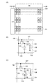
図1(A)に、表示装置の一例を示す。図1(A)に示す表示装置は、画素部100と、走査線駆動回路104と、信号線駆動回路106と、各々が平行または略平行に配置され、かつ走査線駆動回路104によって電位が制御されるm本の走査線107と、各々が平行または略平行に配置され、かつ信号線駆動回路106によって電位が制御されるn本の信号線109と、を有する。さらに、画素部100はマトリクス状に配置された複数の画素101を有する。また、走査線107に沿って、各々が平行または略平行に配置された容量線115を有する。なお、容量線115は、信号線109に沿って、各々が平行または略平行に配置されていてもよい。
本実施の形態では、先の実施の形態1の図3に示す表示装置の第1の基板102上に設けられた素子部の作製方法について、図4および図5を用いて説明する。
まず、第1の基板102に走査線107および容量線115を形成し、走査線107および容量線115を覆うように後にゲート絶縁膜127に加工される絶縁膜126を形成し、絶縁膜126の走査線107と重畳する領域に多層膜111を形成し、後に画素電極121が形成される領域と重畳するように多層膜119を形成する(図4(A)を参照)。
本実施の形態においては、本発明の一態様である表示装置について、実施の形態1に示す構成と異なる構成について、図6乃至図11を用いて説明する。なお、図6乃至図11に示す表示装置においては、液晶層および対向側の第2の基板に形成される素子等については、図3に示す構成と同様であるため、省略して図示している。
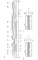
まず、図6および図7を用いて表示装置の構成の変形例1について説明を行う。ここでは、図2および図3で説明した容量素子105と異なる容量素子165についてのみ説明する。図6は画素161の上面図であり、図7は図6の一点鎖線C1−C2間、および一点鎖線D1−D2間の断面図である。
次に、図8および図9を用いて表示装置の構成の変形例2について説明を行う。ここでは、図2および図3で説明した容量素子105と異なる容量素子175について説明する。図8は画素171の上面図であり、図9は図8の一点鎖線E1−E2間、および一点鎖線F1−F2間の断面図である。
次に、図10および図11を用いて表示装置の構成の変形例3について説明を行う。ここでは、図8および図9で説明した容量素子175と異なる容量素子185について説明する。図10は画素181の上面図であり、図11は図10の一点鎖線G1−G2間、および一点鎖線H1−H2間の断面図である。
本実施の形態では、上記実施の形態で説明した表示装置に含まれているトランジスタおよび容量素子において、酸化物半導体層を含む多層膜に適用可能な一態様について説明する。
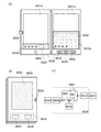
本実施の形態では、上記実施の形態で一例を示した表示装置と、駆動回路の一部または全体を画素部と同じ基板上に一体形成し、システムオンパネルを形成する例について、図12乃至図14を用いて説明する。なお、図13(A)、図13(B)は、図12(B)中でM−Nの一点鎖線で示した部位の断面構成を示す断面図である。なお、図13において、画素部の構造は一部のみ記載している。
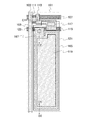
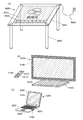
本発明の一態様である表示装置は、さまざまな電子機器(遊技機も含む。)に適用することができる。電子機器としては、テレビジョン装置(テレビ、またはテレビジョン受信機ともいう。)、コンピュータ用などのモニタ、デジタルカメラ、デジタルビデオカメラ、デジタルフォトフレーム、携帯電話機、携帯型ゲーム機、携帯情報端末、音響再生装置、遊技機(パチンコ機、スロットマシン等)、ゲーム筐体が挙げられる。これらの電子機器の一例を図15に示す。
101 画素
102 第1の基板
103 トランジスタ
104 走査線駆動回路
105 容量素子
106 信号線駆動回路
107 走査線
108 液晶素子
109 信号線
111 多層膜
111_1 第1の酸化物層
111_2 第2の酸化物層
111_3 第3の酸化物層
113 導電膜
115 容量線
117 開口
119 多層膜
119_1 第1の酸化物層
119_2 第2の酸化物層
119_3 第3の酸化物層
121 画素電極
123 開口
124 画素電極
125 導電膜
126 絶縁膜
127 ゲート絶縁膜
128 絶縁膜
129 絶縁膜
130 絶縁膜
131 絶縁膜
132 絶縁膜
133 絶縁膜
135 導電膜
137 導電膜
138 開口
139 開口
148 導電膜
149 開口
150 第2の基板
152 遮光膜
154 対向電極
155 配線
156 絶縁膜
158 絶縁膜
160 液晶層
161 画素
165 容量素子
167 導電膜
171 画素
175 容量素子
181 画素
185 容量素子
901 第1の基板
902 画素部
903 信号線駆動回路
904 走査線駆動回路
905 シール材
906 第2の基板
908 液晶層
910 トランジスタ
911 トランジスタ
913 液晶素子
915 接続端子電極
916 端子電極
917 導電膜
918 FPC
918b FPC
919 異方性導電剤
922 ゲート絶縁膜
923 絶縁膜
924 絶縁膜
925 シール材
926 容量素子
927 酸化物半導体膜
928 電極
929 容量配線
930 電極
931 電極
932 絶縁膜
933 絶縁膜
935 スペーサ
940 電極
941 電極
943 液晶素子
945 電極
946 共通配線
971 ソース電極
973 ドレイン電極
975 共通電位線
977 共通電極
985 共通電位線
987 共通電極
9000 テーブル
9001 筐体
9002 脚部
9003 表示部
9004 表示ボタン
9005 電源コード
9033 留め具
9034 スイッチ
9035 電源スイッチ
9036 スイッチ
9038 操作スイッチ
9100 テレビジョン装置
9101 筐体
9103 表示部
9105 スタンド
9107 表示部
9109 操作キー
9110 リモコン操作機
9201 本体
9202 筐体
9203 表示部
9204 キーボード
9205 外部接続ポート
9206 ポインティングデバイス
9630 筐体
9631 表示部
9631a 表示部
9631b 表示部
9632a 領域
9632b 領域
9633 太陽電池
9634 充放電制御回路
9635 バッテリー
9636 DCDCコンバータ
9637 コンバータ
9638 操作キー
9639 ボタン
Claims (14)
- 透光性を有する画素電極と電気的に接続されたトランジスタと、容量素子と
を有し、
前記トランジスタは、
ゲート電極と、前記ゲート電極上に設けられたゲート絶縁膜と、
前記ゲート絶縁膜上に設けられ酸化物半導体層を含む第1の多層膜と
を含み、
前記容量素子は、
前記画素電極と、前記画素電極と重なりかつ所定の間隔を開けて配置された前記第1の多層膜と同じ層構造である第2の多層膜と、を有し、
前記トランジスタのチャネル形成領域は、前記第1の多層膜のうち、前記ゲート絶縁膜と接しない少なくとも一層であること
を特徴とする表示装置。 - 前記第1の多層膜は、
前記ゲート絶縁膜上に接する第1の酸化物層と、
前記第1の酸化物層上に接する第2の酸化物層と、
を含むことを特徴とする
請求項1に記載の表示装置。 - 前記第2の酸化物層は、
前記第1の酸化物層よりも電子親和力が0.2eVよりも大きいことを特徴とする
請求項2に記載の表示装置。 - 前記第1の酸化物層は、
アルミニウム、シリコン、チタン、ガリウム、ゲルマニウム、イットリウム、ジルコニウム、スズ、ランタン、セリウムまたはハフニウムを前記第2の酸化物層よりも1.5倍以上高い濃度で含むことを特徴とする
請求項2または請求項3に記載の表示装置。 - 前記第1の酸化物層および前記第2の酸化物層は、In−Ga−Zn酸化物であり、
前記第1の酸化物層がIn:Ga:Zn=x1:y1:z1[原子数比]、前記第2の酸化物層がIn:Ga:Zn=x2:y2:z2[原子数比]のとき、y1/x1がy2/x2よりも1.5倍以上大きいことを特徴とする
請求項2または請求項3に記載の表示装置。 - 前記第2の酸化物層が結晶質構造であり、
前記第1の酸化物層が前記第2の酸化物層より結晶性の低い構造であることを特徴とする
請求項2乃至請求項5のいずれか一に記載の表示装置。 - 前記第1の多層膜は、
前記ゲート絶縁膜上に接する第1の酸化物層と、
前記第1の酸化物層上に接する第2の酸化物層と、
前記第2の酸化物層上に接する第3の酸化物層と、
を含むことを特徴とする
請求項1に記載の表示装置。 - 前記第2の酸化物層は、
前記第1の酸化物層および前記第3の酸化物層よりも電子親和力が0.2eVよりも大きいことを特徴とする
請求項7に記載の表示装置。 - 前記第1の酸化物層および前記第3の酸化物層は、
アルミニウム、シリコン、チタン、ガリウム、ゲルマニウム、イットリウム、ジルコニウム、スズ、ランタン、セリウムまたはハフニウムを前記第2の酸化物層よりも1.5倍以上高い濃度で含むことを特徴とする
請求項7または請求項8に記載の表示装置。 - 前記第1の酸化物層、前記第2の酸化物層および前記第3の酸化物層は、In−Ga−Zn酸化物であり、
前記第1の酸化物層がIn:Ga:Zn=x1:y1:z1[原子数比]、前記第2の酸化物層がIn:Ga:Zn=x2:y2:z2[原子数比]、前記第3の酸化物層がIn:Ga:Zn=x3:y3:z3[原子数比]のとき、y1/x1およびy3/x3がy2/x2よりも1.5倍以上大きいことを特徴とする
請求項7または請求項8に記載の表示装置。 - 前記第2の酸化物層が結晶質構造であり、
前記第1の酸化物層が前記第2の酸化物層より結晶性の低い構造であることを特徴とする
請求項7乃至請求項10のいずれか一に記載の表示装置。 - 前記第3の酸化物層が結晶質構造であることを特徴とする
請求項11に記載の表示装置。 - 前記ゲート電極と同一工程で形成した容量線を有し、
前記第2の多層膜は、前記容量線に電気的に接続される
ことを特徴とする請求項1乃至請求項12のいずれか一に記載の表示装置。 - 請求項1乃至請求項13のいずれか一に記載の表示装置を用いた電子機器。
Priority Applications (1)
| Application Number | Priority Date | Filing Date | Title |
|---|---|---|---|
| JP2013187215A JP2014075581A (ja) | 2012-09-13 | 2013-09-10 | 表示装置および電子機器 |
Applications Claiming Priority (3)
| Application Number | Priority Date | Filing Date | Title |
|---|---|---|---|
| JP2012202123 | 2012-09-13 | ||
| JP2012202123 | 2012-09-13 | ||
| JP2013187215A JP2014075581A (ja) | 2012-09-13 | 2013-09-10 | 表示装置および電子機器 |
Related Child Applications (1)
| Application Number | Title | Priority Date | Filing Date |
|---|---|---|---|
| JP2018015127A Division JP6499336B2 (ja) | 2012-09-13 | 2018-01-31 | 表示装置 |
Publications (2)
| Publication Number | Publication Date |
|---|---|
| JP2014075581A true JP2014075581A (ja) | 2014-04-24 |
| JP2014075581A5 JP2014075581A5 (ja) | 2016-10-06 |
Family
ID=50232331
Family Applications (6)
| Application Number | Title | Priority Date | Filing Date |
|---|---|---|---|
| JP2013187215A Withdrawn JP2014075581A (ja) | 2012-09-13 | 2013-09-10 | 表示装置および電子機器 |
| JP2018015127A Active JP6499336B2 (ja) | 2012-09-13 | 2018-01-31 | 表示装置 |
| JP2019046991A Active JP6710301B2 (ja) | 2012-09-13 | 2019-03-14 | 表示装置、および電子機器 |
| JP2020091142A Withdrawn JP2020145469A (ja) | 2012-09-13 | 2020-05-26 | 表示装置 |
| JP2022047866A Active JP7340645B2 (ja) | 2012-09-13 | 2022-03-24 | 表示装置 |
| JP2023138179A Pending JP2023164887A (ja) | 2012-09-13 | 2023-08-28 | 表示装置 |
Family Applications After (5)
| Application Number | Title | Priority Date | Filing Date |
|---|---|---|---|
| JP2018015127A Active JP6499336B2 (ja) | 2012-09-13 | 2018-01-31 | 表示装置 |
| JP2019046991A Active JP6710301B2 (ja) | 2012-09-13 | 2019-03-14 | 表示装置、および電子機器 |
| JP2020091142A Withdrawn JP2020145469A (ja) | 2012-09-13 | 2020-05-26 | 表示装置 |
| JP2022047866A Active JP7340645B2 (ja) | 2012-09-13 | 2022-03-24 | 表示装置 |
| JP2023138179A Pending JP2023164887A (ja) | 2012-09-13 | 2023-08-28 | 表示装置 |
Country Status (2)
| Country | Link |
|---|---|
| US (3) | US9018624B2 (ja) |
| JP (6) | JP2014075581A (ja) |
Cited By (1)
| Publication number | Priority date | Publication date | Assignee | Title |
|---|---|---|---|---|
| KR20180062373A (ko) * | 2016-11-30 | 2018-06-08 | 가부시키가이샤 한도오따이 에네루기 켄큐쇼 | 표시 장치, 표시 모듈, 및 전자 기기 |
Families Citing this family (29)
| Publication number | Priority date | Publication date | Assignee | Title |
|---|---|---|---|---|
| WO2011004723A1 (en) * | 2009-07-10 | 2011-01-13 | Semiconductor Energy Laboratory Co., Ltd. | Semiconductor device and manufacturing method the same |
| US8981372B2 (en) | 2012-09-13 | 2015-03-17 | Semiconductor Energy Laboratory Co., Ltd. | Display device and electronic appliance |
| US8927985B2 (en) | 2012-09-20 | 2015-01-06 | Semiconductor Energy Laboratory Co., Ltd. | Semiconductor device |
| WO2014103901A1 (en) | 2012-12-25 | 2014-07-03 | Semiconductor Energy Laboratory Co., Ltd. | Semiconductor device and method for manufacturing the same |
| US9269315B2 (en) | 2013-03-08 | 2016-02-23 | Semiconductor Energy Laboratory Co., Ltd. | Driving method of semiconductor device |
| US9704894B2 (en) | 2013-05-10 | 2017-07-11 | Semiconductor Energy Laboratory Co., Ltd. | Display device including pixel electrode including oxide |
| KR102244553B1 (ko) | 2013-08-23 | 2021-04-23 | 가부시키가이샤 한도오따이 에네루기 켄큐쇼 | 용량 소자 및 반도체 장치 |
| KR102099881B1 (ko) * | 2013-09-03 | 2020-05-15 | 삼성전자 주식회사 | 반도체 소자 및 그 제조 방법 |
| TWI646690B (zh) | 2013-09-13 | 2019-01-01 | 半導體能源研究所股份有限公司 | 半導體裝置及其製造方法 |
| JP2015179247A (ja) | 2013-10-22 | 2015-10-08 | 株式会社半導体エネルギー研究所 | 表示装置 |
| TWI721409B (zh) | 2013-12-19 | 2021-03-11 | 日商半導體能源研究所股份有限公司 | 半導體裝置 |
| JP6506545B2 (ja) | 2013-12-27 | 2019-04-24 | 株式会社半導体エネルギー研究所 | 半導体装置 |
| TWI657488B (zh) * | 2014-03-20 | 2019-04-21 | 日商半導體能源研究所股份有限公司 | 半導體裝置、具有該半導體裝置的顯示裝置、具有該顯示裝置的顯示模組以及具有該半導體裝置、該顯示裝置和該顯示模組的電子裝置 |
| JP6722980B2 (ja) * | 2014-05-09 | 2020-07-15 | 株式会社半導体エネルギー研究所 | 表示装置および発光装置、並びに電子機器 |
| TWI663726B (zh) | 2014-05-30 | 2019-06-21 | Semiconductor Energy Laboratory Co., Ltd. | 半導體裝置、模組及電子裝置 |
| US20160023569A1 (en) * | 2014-07-28 | 2016-01-28 | Ford Global Technologies, Llc | Battery power capability estimation based on reduced order electrochemical models |
| US9766517B2 (en) | 2014-09-05 | 2017-09-19 | Semiconductor Energy Laboratory Co., Ltd. | Display device and display module |
| WO2016063169A1 (en) | 2014-10-23 | 2016-04-28 | Semiconductor Energy Laboratory Co., Ltd. | Light-emitting element |
| US10680017B2 (en) | 2014-11-07 | 2020-06-09 | Semiconductor Energy Laboratory Co., Ltd. | Light-emitting element including EL layer, electrode which has high reflectance and a high work function, display device, electronic device, and lighting device |
| KR20160114511A (ko) | 2015-03-24 | 2016-10-05 | 가부시키가이샤 한도오따이 에네루기 켄큐쇼 | 반도체 장치의 제작 방법 |
| US9806200B2 (en) | 2015-03-27 | 2017-10-31 | Semiconductor Energy Laboratory Co., Ltd. | Semiconductor device |
| US10714633B2 (en) | 2015-12-15 | 2020-07-14 | Semiconductor Energy Laboratory Co., Ltd. | Semiconductor device and display device |
| WO2017153882A1 (en) | 2016-03-11 | 2017-09-14 | Semiconductor Energy Laboratory Co., Ltd. | Semiconductor device, manufacturing method thereof, and display device including the semiconductor device |
| KR102384624B1 (ko) * | 2016-10-21 | 2022-04-11 | 가부시키가이샤 한도오따이 에네루기 켄큐쇼 | 반도체 장치 |
| US20180145096A1 (en) | 2016-11-23 | 2018-05-24 | Semiconductor Energy Laboratory Co., Ltd. | Display device and electronic device |
| JP7367414B2 (ja) * | 2019-09-10 | 2023-10-24 | セイコーエプソン株式会社 | 電気光学装置、電気光学装置の製造方法および電子機器 |
| CN111210732B (zh) * | 2020-03-06 | 2022-06-21 | 合肥维信诺科技有限公司 | 显示面板和显示装置 |
| US11335391B1 (en) | 2020-10-30 | 2022-05-17 | Ferroelectric Memory Gmbh | Memory cell arrangement and method thereof |
| US11527551B2 (en) * | 2020-10-30 | 2022-12-13 | Ferroelectric Memory Gmbh | Memory cell arrangements and methods thereof |
Citations (3)
| Publication number | Priority date | Publication date | Assignee | Title |
|---|---|---|---|---|
| JP2011124360A (ja) * | 2009-12-10 | 2011-06-23 | Fujifilm Corp | 薄膜トランジスタおよびその製造方法、並びにその薄膜トランジスタを備えた装置 |
| US8102476B2 (en) * | 2007-12-03 | 2012-01-24 | Samsung Electronics Co., Ltd. | Display devices including an oxide semiconductor thin film transistor |
| WO2012086513A1 (ja) * | 2010-12-20 | 2012-06-28 | シャープ株式会社 | 半導体装置および表示装置 |
Family Cites Families (166)
| Publication number | Priority date | Publication date | Assignee | Title |
|---|---|---|---|---|
| JPS60198861A (ja) | 1984-03-23 | 1985-10-08 | Fujitsu Ltd | 薄膜トランジスタ |
| JPH07104312B2 (ja) | 1986-03-25 | 1995-11-13 | 株式会社東芝 | 攪拌電極装置 |
| JPH0244256B2 (ja) | 1987-01-28 | 1990-10-03 | Kagaku Gijutsucho Mukizaishitsu Kenkyushocho | Ingazn2o5deshimesarerurotsuhoshokeinosojokozoojusurukagobutsuoyobisonoseizoho |
| JPH0244258B2 (ja) | 1987-02-24 | 1990-10-03 | Kagaku Gijutsucho Mukizaishitsu Kenkyushocho | Ingazn3o6deshimesarerurotsuhoshokeinosojokozoojusurukagobutsuoyobisonoseizoho |
| JPH0244260B2 (ja) | 1987-02-24 | 1990-10-03 | Kagaku Gijutsucho Mukizaishitsu Kenkyushocho | Ingazn5o8deshimesarerurotsuhoshokeinosojokozoojusurukagobutsuoyobisonoseizoho |
| JPS63210023A (ja) | 1987-02-24 | 1988-08-31 | Natl Inst For Res In Inorg Mater | InGaZn↓4O↓7で示される六方晶系の層状構造を有する化合物およびその製造法 |
| JPH0244262B2 (ja) | 1987-02-27 | 1990-10-03 | Kagaku Gijutsucho Mukizaishitsu Kenkyushocho | Ingazn6o9deshimesarerurotsuhoshokeinosojokozoojusurukagobutsuoyobisonoseizoho |
| JPH0244263B2 (ja) | 1987-04-22 | 1990-10-03 | Kagaku Gijutsucho Mukizaishitsu Kenkyushocho | Ingazn7o10deshimesarerurotsuhoshokeinosojokozoojusurukagobutsuoyobisonoseizoho |
| JPH05216072A (ja) * | 1992-02-04 | 1993-08-27 | Sony Corp | 液晶表示装置 |
| JPH05251705A (ja) | 1992-03-04 | 1993-09-28 | Fuji Xerox Co Ltd | 薄膜トランジスタ |
| JPH05297412A (ja) * | 1992-04-22 | 1993-11-12 | Nippon Steel Corp | 液晶表示装置 |
| FR2702286B1 (fr) * | 1993-03-04 | 1998-01-30 | Samsung Electronics Co Ltd | Affichage à cristaux liquides et procédé pour le fabriquer. |
| US5416356A (en) * | 1993-09-03 | 1995-05-16 | Motorola, Inc. | Integrated circuit having passive circuit elements |
| JPH07104312A (ja) | 1993-09-30 | 1995-04-21 | Sanyo Electric Co Ltd | 液晶表示装置の製造方法 |
| JP3479375B2 (ja) | 1995-03-27 | 2003-12-15 | 科学技術振興事業団 | 亜酸化銅等の金属酸化物半導体による薄膜トランジスタとpn接合を形成した金属酸化物半導体装置およびそれらの製造方法 |
| WO1997006554A2 (en) | 1995-08-03 | 1997-02-20 | Philips Electronics N.V. | Semiconductor device provided with transparent switching element |
| JP3625598B2 (ja) | 1995-12-30 | 2005-03-02 | 三星電子株式会社 | 液晶表示装置の製造方法 |
| JP4170454B2 (ja) | 1998-07-24 | 2008-10-22 | Hoya株式会社 | 透明導電性酸化物薄膜を有する物品及びその製造方法 |
| JP2000150861A (ja) | 1998-11-16 | 2000-05-30 | Tdk Corp | 酸化物薄膜 |
| JP3276930B2 (ja) | 1998-11-17 | 2002-04-22 | 科学技術振興事業団 | トランジスタ及び半導体装置 |
| US8158980B2 (en) * | 2001-04-19 | 2012-04-17 | Semiconductor Energy Laboratory Co., Ltd. | Semiconductor device having a pixel matrix circuit that includes a pixel TFT and a storage capacitor |
| US7122835B1 (en) | 1999-04-07 | 2006-10-17 | Semiconductor Energy Laboratory Co., Ltd. | Electrooptical device and a method of manufacturing the same |
| JP3746924B2 (ja) * | 1999-08-26 | 2006-02-22 | 鹿児島日本電気株式会社 | 液晶表示装置のアクティブパネルの製造方法 |
| TW460731B (en) | 1999-09-03 | 2001-10-21 | Ind Tech Res Inst | Electrode structure and production method of wide viewing angle LCD |
| JP4089858B2 (ja) | 2000-09-01 | 2008-05-28 | 国立大学法人東北大学 | 半導体デバイス |
| KR20020038482A (ko) | 2000-11-15 | 2002-05-23 | 모리시타 요이찌 | 박막 트랜지스터 어레이, 그 제조방법 및 그것을 이용한표시패널 |
| JP3997731B2 (ja) | 2001-03-19 | 2007-10-24 | 富士ゼロックス株式会社 | 基材上に結晶性半導体薄膜を形成する方法 |
| JP2002289859A (ja) | 2001-03-23 | 2002-10-04 | Minolta Co Ltd | 薄膜トランジスタ |
| JP3925839B2 (ja) | 2001-09-10 | 2007-06-06 | シャープ株式会社 | 半導体記憶装置およびその試験方法 |
| JP4090716B2 (ja) | 2001-09-10 | 2008-05-28 | 雅司 川崎 | 薄膜トランジスタおよびマトリクス表示装置 |
| WO2003040441A1 (en) | 2001-11-05 | 2003-05-15 | Japan Science And Technology Agency | Natural superlattice homologous single crystal thin film, method for preparation thereof, and device using said single crystal thin film |
| JP4164562B2 (ja) | 2002-09-11 | 2008-10-15 | 独立行政法人科学技術振興機構 | ホモロガス薄膜を活性層として用いる透明薄膜電界効果型トランジスタ |
| JP4083486B2 (ja) | 2002-02-21 | 2008-04-30 | 独立行政法人科学技術振興機構 | LnCuO(S,Se,Te)単結晶薄膜の製造方法 |
| US7049190B2 (en) | 2002-03-15 | 2006-05-23 | Sanyo Electric Co., Ltd. | Method for forming ZnO film, method for forming ZnO semiconductor layer, method for fabricating semiconductor device, and semiconductor device |
| JP3933591B2 (ja) | 2002-03-26 | 2007-06-20 | 淳二 城戸 | 有機エレクトロルミネッセント素子 |
| US7339187B2 (en) | 2002-05-21 | 2008-03-04 | State Of Oregon Acting By And Through The Oregon State Board Of Higher Education On Behalf Of Oregon State University | Transistor structures |
| JP2004022625A (ja) | 2002-06-13 | 2004-01-22 | Murata Mfg Co Ltd | 半導体デバイス及び該半導体デバイスの製造方法 |
| US7105868B2 (en) | 2002-06-24 | 2006-09-12 | Cermet, Inc. | High-electron mobility transistor with zinc oxide |
| US7067843B2 (en) | 2002-10-11 | 2006-06-27 | E. I. Du Pont De Nemours And Company | Transparent oxide semiconductor thin film transistors |
| JP4166105B2 (ja) | 2003-03-06 | 2008-10-15 | シャープ株式会社 | 半導体装置およびその製造方法 |
| JP2004273732A (ja) | 2003-03-07 | 2004-09-30 | Sharp Corp | アクティブマトリクス基板およびその製造方法 |
| JP4108633B2 (ja) | 2003-06-20 | 2008-06-25 | シャープ株式会社 | 薄膜トランジスタおよびその製造方法ならびに電子デバイス |
| US7262463B2 (en) | 2003-07-25 | 2007-08-28 | Hewlett-Packard Development Company, L.P. | Transistor including a deposited channel region having a doped portion |
| JP4483235B2 (ja) | 2003-09-01 | 2010-06-16 | カシオ計算機株式会社 | トランジスタアレイ基板の製造方法及びトランジスタアレイ基板 |
| US7282782B2 (en) | 2004-03-12 | 2007-10-16 | Hewlett-Packard Development Company, L.P. | Combined binary oxide semiconductor device |
| US7145174B2 (en) | 2004-03-12 | 2006-12-05 | Hewlett-Packard Development Company, Lp. | Semiconductor device |
| US7297977B2 (en) | 2004-03-12 | 2007-11-20 | Hewlett-Packard Development Company, L.P. | Semiconductor device |
| KR101078509B1 (ko) | 2004-03-12 | 2011-10-31 | 도꾸리쯔교세이호징 가가꾸 기쥬쯔 신꼬 기꼬 | 박막 트랜지스터의 제조 방법 |
| US7211825B2 (en) | 2004-06-14 | 2007-05-01 | Yi-Chi Shih | Indium oxide-based thin film transistors and circuits |
| JP2006100760A (ja) | 2004-09-02 | 2006-04-13 | Casio Comput Co Ltd | 薄膜トランジスタおよびその製造方法 |
| US7285501B2 (en) | 2004-09-17 | 2007-10-23 | Hewlett-Packard Development Company, L.P. | Method of forming a solution processed device |
| US7298084B2 (en) | 2004-11-02 | 2007-11-20 | 3M Innovative Properties Company | Methods and displays utilizing integrated zinc oxide row and column drivers in conjunction with organic light emitting diodes |
| CN102938420B (zh) | 2004-11-10 | 2015-12-02 | 佳能株式会社 | 无定形氧化物和场效应晶体管 |
| US7453065B2 (en) | 2004-11-10 | 2008-11-18 | Canon Kabushiki Kaisha | Sensor and image pickup device |
| US7791072B2 (en) | 2004-11-10 | 2010-09-07 | Canon Kabushiki Kaisha | Display |
| US7863611B2 (en) | 2004-11-10 | 2011-01-04 | Canon Kabushiki Kaisha | Integrated circuits utilizing amorphous oxides |
| CA2585071A1 (en) | 2004-11-10 | 2006-05-18 | Canon Kabushiki Kaisha | Field effect transistor employing an amorphous oxide |
| US7829444B2 (en) | 2004-11-10 | 2010-11-09 | Canon Kabushiki Kaisha | Field effect transistor manufacturing method |
| WO2006051994A2 (en) | 2004-11-10 | 2006-05-18 | Canon Kabushiki Kaisha | Light-emitting device |
| US7579224B2 (en) | 2005-01-21 | 2009-08-25 | Semiconductor Energy Laboratory Co., Ltd. | Method for manufacturing a thin film semiconductor device |
| TWI472037B (zh) | 2005-01-28 | 2015-02-01 | Semiconductor Energy Lab | 半導體裝置,電子裝置,和半導體裝置的製造方法 |
| TWI569441B (zh) | 2005-01-28 | 2017-02-01 | 半導體能源研究所股份有限公司 | 半導體裝置,電子裝置,和半導體裝置的製造方法 |
| US7858451B2 (en) | 2005-02-03 | 2010-12-28 | Semiconductor Energy Laboratory Co., Ltd. | Electronic device, semiconductor device and manufacturing method thereof |
| US7948171B2 (en) | 2005-02-18 | 2011-05-24 | Semiconductor Energy Laboratory Co., Ltd. | Light emitting device |
| US20060197092A1 (en) | 2005-03-03 | 2006-09-07 | Randy Hoffman | System and method for forming conductive material on a substrate |
| US8681077B2 (en) | 2005-03-18 | 2014-03-25 | Semiconductor Energy Laboratory Co., Ltd. | Semiconductor device, and display device, driving method and electronic apparatus thereof |
| WO2006105077A2 (en) | 2005-03-28 | 2006-10-05 | Massachusetts Institute Of Technology | Low voltage thin film transistor with high-k dielectric material |
| US7645478B2 (en) | 2005-03-31 | 2010-01-12 | 3M Innovative Properties Company | Methods of making displays |
| US8300031B2 (en) | 2005-04-20 | 2012-10-30 | Semiconductor Energy Laboratory Co., Ltd. | Semiconductor device comprising transistor having gate and drain connected through a current-voltage conversion element |
| JP2006344849A (ja) | 2005-06-10 | 2006-12-21 | Casio Comput Co Ltd | 薄膜トランジスタ |
| US7402506B2 (en) | 2005-06-16 | 2008-07-22 | Eastman Kodak Company | Methods of making thin film transistors comprising zinc-oxide-based semiconductor materials and transistors made thereby |
| US7691666B2 (en) | 2005-06-16 | 2010-04-06 | Eastman Kodak Company | Methods of making thin film transistors comprising zinc-oxide-based semiconductor materials and transistors made thereby |
| US7507618B2 (en) | 2005-06-27 | 2009-03-24 | 3M Innovative Properties Company | Method for making electronic devices using metal oxide nanoparticles |
| KR100711890B1 (ko) | 2005-07-28 | 2007-04-25 | 삼성에스디아이 주식회사 | 유기 발광표시장치 및 그의 제조방법 |
| JP2007059128A (ja) | 2005-08-23 | 2007-03-08 | Canon Inc | 有機el表示装置およびその製造方法 |
| JP4850457B2 (ja) | 2005-09-06 | 2012-01-11 | キヤノン株式会社 | 薄膜トランジスタ及び薄膜ダイオード |
| JP5116225B2 (ja) | 2005-09-06 | 2013-01-09 | キヤノン株式会社 | 酸化物半導体デバイスの製造方法 |
| JP4280736B2 (ja) | 2005-09-06 | 2009-06-17 | キヤノン株式会社 | 半導体素子 |
| JP2007073705A (ja) | 2005-09-06 | 2007-03-22 | Canon Inc | 酸化物半導体チャネル薄膜トランジスタおよびその製造方法 |
| EP1995787A3 (en) | 2005-09-29 | 2012-01-18 | Semiconductor Energy Laboratory Co, Ltd. | Semiconductor device having oxide semiconductor layer and manufacturing method therof |
| JP5078246B2 (ja) | 2005-09-29 | 2012-11-21 | 株式会社半導体エネルギー研究所 | 半導体装置、及び半導体装置の作製方法 |
| JP5064747B2 (ja) | 2005-09-29 | 2012-10-31 | 株式会社半導体エネルギー研究所 | 半導体装置、電気泳動表示装置、表示モジュール、電子機器、及び半導体装置の作製方法 |
| JP5037808B2 (ja) | 2005-10-20 | 2012-10-03 | キヤノン株式会社 | アモルファス酸化物を用いた電界効果型トランジスタ、及び該トランジスタを用いた表示装置 |
| CN101707212B (zh) | 2005-11-15 | 2012-07-11 | 株式会社半导体能源研究所 | 半导体器件及其制造方法 |
| TWI292281B (en) | 2005-12-29 | 2008-01-01 | Ind Tech Res Inst | Pixel structure of active organic light emitting diode and method of fabricating the same |
| US7867636B2 (en) | 2006-01-11 | 2011-01-11 | Murata Manufacturing Co., Ltd. | Transparent conductive film and method for manufacturing the same |
| JP4977478B2 (ja) | 2006-01-21 | 2012-07-18 | 三星電子株式会社 | ZnOフィルム及びこれを用いたTFTの製造方法 |
| US7576394B2 (en) | 2006-02-02 | 2009-08-18 | Kochi Industrial Promotion Center | Thin film transistor including low resistance conductive thin films and manufacturing method thereof |
| US7977169B2 (en) | 2006-02-15 | 2011-07-12 | Kochi Industrial Promotion Center | Semiconductor device including active layer made of zinc oxide with controlled orientations and manufacturing method thereof |
| EP1843194A1 (en) | 2006-04-06 | 2007-10-10 | Semiconductor Energy Laboratory Co., Ltd. | Liquid crystal display device, semiconductor device, and electronic appliance |
| KR20070101595A (ko) | 2006-04-11 | 2007-10-17 | 삼성전자주식회사 | ZnO TFT |
| US20070252928A1 (en) | 2006-04-28 | 2007-11-01 | Toppan Printing Co., Ltd. | Structure, transmission type liquid crystal display, reflection type display and manufacturing method thereof |
| JP5028033B2 (ja) | 2006-06-13 | 2012-09-19 | キヤノン株式会社 | 酸化物半導体膜のドライエッチング方法 |
| JP4609797B2 (ja) | 2006-08-09 | 2011-01-12 | Nec液晶テクノロジー株式会社 | 薄膜デバイス及びその製造方法 |
| JP4999400B2 (ja) | 2006-08-09 | 2012-08-15 | キヤノン株式会社 | 酸化物半導体膜のドライエッチング方法 |
| JP4332545B2 (ja) | 2006-09-15 | 2009-09-16 | キヤノン株式会社 | 電界効果型トランジスタ及びその製造方法 |
| JP5164357B2 (ja) | 2006-09-27 | 2013-03-21 | キヤノン株式会社 | 半導体装置及び半導体装置の製造方法 |
| JP4274219B2 (ja) | 2006-09-27 | 2009-06-03 | セイコーエプソン株式会社 | 電子デバイス、有機エレクトロルミネッセンス装置、有機薄膜半導体装置 |
| US7622371B2 (en) | 2006-10-10 | 2009-11-24 | Hewlett-Packard Development Company, L.P. | Fused nanocrystal thin film semiconductor and method |
| US7772021B2 (en) | 2006-11-29 | 2010-08-10 | Samsung Electronics Co., Ltd. | Flat panel displays comprising a thin-film transistor having a semiconductive oxide in its channel and methods of fabricating the same for use in flat panel displays |
| JP2008140684A (ja) | 2006-12-04 | 2008-06-19 | Toppan Printing Co Ltd | カラーelディスプレイおよびその製造方法 |
| KR101303578B1 (ko) | 2007-01-05 | 2013-09-09 | 삼성전자주식회사 | 박막 식각 방법 |
| US8207063B2 (en) | 2007-01-26 | 2012-06-26 | Eastman Kodak Company | Process for atomic layer deposition |
| JP5121254B2 (ja) | 2007-02-28 | 2013-01-16 | キヤノン株式会社 | 薄膜トランジスタおよび表示装置 |
| KR100851215B1 (ko) | 2007-03-14 | 2008-08-07 | 삼성에스디아이 주식회사 | 박막 트랜지스터 및 이를 이용한 유기 전계 발광표시장치 |
| US7795613B2 (en) | 2007-04-17 | 2010-09-14 | Toppan Printing Co., Ltd. | Structure with transistor |
| KR101325053B1 (ko) | 2007-04-18 | 2013-11-05 | 삼성디스플레이 주식회사 | 박막 트랜지스터 기판 및 이의 제조 방법 |
| KR20080094300A (ko) | 2007-04-19 | 2008-10-23 | 삼성전자주식회사 | 박막 트랜지스터 및 그 제조 방법과 박막 트랜지스터를포함하는 평판 디스플레이 |
| KR101334181B1 (ko) | 2007-04-20 | 2013-11-28 | 삼성전자주식회사 | 선택적으로 결정화된 채널층을 갖는 박막 트랜지스터 및 그제조 방법 |
| CN101663762B (zh) | 2007-04-25 | 2011-09-21 | 佳能株式会社 | 氧氮化物半导体 |
| KR101345376B1 (ko) | 2007-05-29 | 2013-12-24 | 삼성전자주식회사 | ZnO 계 박막 트랜지스터 및 그 제조방법 |
| JP5235363B2 (ja) * | 2007-09-04 | 2013-07-10 | 株式会社ジャパンディスプレイイースト | 液晶表示装置 |
| US8202365B2 (en) | 2007-12-17 | 2012-06-19 | Fujifilm Corporation | Process for producing oriented inorganic crystalline film, and semiconductor device using the oriented inorganic crystalline film |
| JP4555358B2 (ja) | 2008-03-24 | 2010-09-29 | 富士フイルム株式会社 | 薄膜電界効果型トランジスタおよび表示装置 |
| KR100941850B1 (ko) | 2008-04-03 | 2010-02-11 | 삼성모바일디스플레이주식회사 | 박막 트랜지스터, 그의 제조 방법 및 박막 트랜지스터를구비하는 평판 표시 장치 |
| JP5430248B2 (ja) | 2008-06-24 | 2014-02-26 | 富士フイルム株式会社 | 薄膜電界効果型トランジスタおよび表示装置 |
| KR100963027B1 (ko) | 2008-06-30 | 2010-06-10 | 삼성모바일디스플레이주식회사 | 박막 트랜지스터, 그의 제조 방법 및 박막 트랜지스터를구비하는 평판 표시 장치 |
| KR100963026B1 (ko) | 2008-06-30 | 2010-06-10 | 삼성모바일디스플레이주식회사 | 박막 트랜지스터, 그의 제조 방법 및 박막 트랜지스터를구비하는 평판 표시 장치 |
| US8945981B2 (en) | 2008-07-31 | 2015-02-03 | Semiconductor Energy Laboratory Co., Ltd. | Semiconductor device and manufacturing method thereof |
| JP5345456B2 (ja) | 2008-08-14 | 2013-11-20 | 富士フイルム株式会社 | 薄膜電界効果型トランジスタ |
| US9082857B2 (en) | 2008-09-01 | 2015-07-14 | Semiconductor Energy Laboratory Co., Ltd. | Semiconductor device comprising an oxide semiconductor layer |
| JP4623179B2 (ja) | 2008-09-18 | 2011-02-02 | ソニー株式会社 | 薄膜トランジスタおよびその製造方法 |
| JP5451280B2 (ja) | 2008-10-09 | 2014-03-26 | キヤノン株式会社 | ウルツ鉱型結晶成長用基板およびその製造方法ならびに半導体装置 |
| KR101310473B1 (ko) * | 2008-10-24 | 2013-09-24 | 가부시키가이샤 한도오따이 에네루기 켄큐쇼 | 반도체 장치 |
| TWI656645B (zh) | 2008-11-13 | 2019-04-11 | 日商半導體能源研究所股份有限公司 | 半導體裝置及其製造方法 |
| EP2515337B1 (en) | 2008-12-24 | 2016-02-24 | Semiconductor Energy Laboratory Co., Ltd. | Driver circuit and semiconductor device |
| JP5606682B2 (ja) | 2009-01-29 | 2014-10-15 | 富士フイルム株式会社 | 薄膜トランジスタ、多結晶酸化物半導体薄膜の製造方法、及び薄膜トランジスタの製造方法 |
| US8436350B2 (en) | 2009-01-30 | 2013-05-07 | Semiconductor Energy Laboratory Co., Ltd. | Semiconductor device using an oxide semiconductor with a plurality of metal clusters |
| JP5439878B2 (ja) * | 2009-03-13 | 2014-03-12 | セイコーエプソン株式会社 | 半導体装置の製造方法、半導体装置、電気光学装置および電子機器 |
| US8822988B2 (en) * | 2009-03-31 | 2014-09-02 | Hewlett-Packard Development Company, L.P. | Thin-film transistor (TFT) with a bi-layer channel |
| JP4571221B1 (ja) | 2009-06-22 | 2010-10-27 | 富士フイルム株式会社 | Igzo系酸化物材料及びigzo系酸化物材料の製造方法 |
| JP4415062B1 (ja) | 2009-06-22 | 2010-02-17 | 富士フイルム株式会社 | 薄膜トランジスタ及び薄膜トランジスタの製造方法 |
| KR101782176B1 (ko) | 2009-07-18 | 2017-09-26 | 가부시키가이샤 한도오따이 에네루기 켄큐쇼 | 반도체 장치 및 반도체 장치의 제조 방법 |
| WO2011010542A1 (en) | 2009-07-23 | 2011-01-27 | Semiconductor Energy Laboratory Co., Ltd. | Semiconductor device and method for manufacturing the same |
| CN102473734B (zh) | 2009-07-31 | 2015-08-12 | 株式会社半导体能源研究所 | 半导体装置及其制造方法 |
| JP2011066375A (ja) | 2009-08-18 | 2011-03-31 | Fujifilm Corp | 非晶質酸化物半導体材料、電界効果型トランジスタ及び表示装置 |
| CN102473736A (zh) | 2009-09-01 | 2012-05-23 | 夏普株式会社 | 半导体装置、有源矩阵基板以及显示装置 |
| WO2011043163A1 (en) | 2009-10-05 | 2011-04-14 | Semiconductor Energy Laboratory Co., Ltd. | Semiconductor device and manufacturing method thereof |
| WO2011046010A1 (en) | 2009-10-16 | 2011-04-21 | Semiconductor Energy Laboratory Co., Ltd. | Liquid crystal display device and electronic device including the liquid crystal display device |
| EP2494601A4 (en) | 2009-10-30 | 2016-09-07 | Semiconductor Energy Lab | SEMICONDUCTOR COMPONENT AND MANUFACTURING METHOD THEREFOR |
| KR101818265B1 (ko) | 2009-11-06 | 2018-01-12 | 가부시키가이샤 한도오따이 에네루기 켄큐쇼 | 반도체 장치 |
| KR20190109597A (ko) | 2009-11-20 | 2019-09-25 | 가부시키가이샤 한도오따이 에네루기 켄큐쇼 | 트랜지스터 |
| KR102068463B1 (ko) | 2009-11-28 | 2020-01-22 | 가부시키가이샤 한도오따이 에네루기 켄큐쇼 | 적층 산화물 재료, 반도체 장치 및 반도체 장치의 제작 방법 |
| WO2011074407A1 (en) | 2009-12-18 | 2011-06-23 | Semiconductor Energy Laboratory Co., Ltd. | Semiconductor device and method for manufacturing the same |
| JP2011138934A (ja) | 2009-12-28 | 2011-07-14 | Sony Corp | 薄膜トランジスタ、表示装置および電子機器 |
| JP2011187506A (ja) | 2010-03-04 | 2011-09-22 | Sony Corp | 薄膜トランジスタおよびその製造方法、並びに表示装置 |
| US8653514B2 (en) | 2010-04-09 | 2014-02-18 | Semiconductor Energy Laboratory Co., Ltd. | Semiconductor device and method for manufacturing the same |
| US8791463B2 (en) * | 2010-04-21 | 2014-07-29 | Sharp Kabushiki Kaisha | Thin-film transistor substrate |
| DE112011101395B4 (de) | 2010-04-23 | 2014-10-16 | Semiconductor Energy Laboratory Co., Ltd. | Verfahren zum Herstellen einer Halbleitervorrichtung |
| JP5133468B2 (ja) | 2010-05-24 | 2013-01-30 | シャープ株式会社 | 薄膜トランジスタ基板及びその製造方法 |
| KR102143469B1 (ko) | 2010-07-27 | 2020-08-11 | 가부시키가이샤 한도오따이 에네루기 켄큐쇼 | 반도체 장치 및 그 제작 방법 |
| US9230994B2 (en) | 2010-09-15 | 2016-01-05 | Semiconductor Energy Laboratory Co., Ltd. | Liquid crystal display device |
| KR20120039947A (ko) * | 2010-10-18 | 2012-04-26 | 삼성모바일디스플레이주식회사 | 표시 장치 및 그 제조 방법 |
| TWI525818B (zh) | 2010-11-30 | 2016-03-11 | 半導體能源研究所股份有限公司 | 半導體裝置及半導體裝置之製造方法 |
| TWI432865B (zh) * | 2010-12-01 | 2014-04-01 | Au Optronics Corp | 畫素結構及其製作方法 |
| JP2012160679A (ja) | 2011-02-03 | 2012-08-23 | Sony Corp | 薄膜トランジスタ、表示装置および電子機器 |
| KR20130007426A (ko) | 2011-06-17 | 2013-01-18 | 가부시키가이샤 한도오따이 에네루기 켄큐쇼 | 반도체 장치 및 그 제작 방법 |
| JP6013685B2 (ja) | 2011-07-22 | 2016-10-25 | 株式会社半導体エネルギー研究所 | 半導体装置 |
| US8748240B2 (en) | 2011-12-22 | 2014-06-10 | Semiconductor Energy Laboratory Co., Ltd. | Method for manufacturing semiconductor device |
| TWI580047B (zh) | 2011-12-23 | 2017-04-21 | 半導體能源研究所股份有限公司 | 半導體裝置 |
| JP5917385B2 (ja) | 2011-12-27 | 2016-05-11 | 株式会社半導体エネルギー研究所 | 半導体装置の作製方法 |
| TWI604609B (zh) | 2012-02-02 | 2017-11-01 | 半導體能源研究所股份有限公司 | 半導體裝置 |
| WO2014021356A1 (en) | 2012-08-03 | 2014-02-06 | Semiconductor Energy Laboratory Co., Ltd. | Semiconductor device |
| TWI657539B (zh) | 2012-08-31 | 2019-04-21 | 日商半導體能源研究所股份有限公司 | 半導體裝置 |
| US8981372B2 (en) | 2012-09-13 | 2015-03-17 | Semiconductor Energy Laboratory Co., Ltd. | Display device and electronic appliance |
| CN111477634B (zh) | 2012-09-13 | 2023-11-14 | 株式会社半导体能源研究所 | 半导体装置 |
-
2013
- 2013-09-05 US US14/018,770 patent/US9018624B2/en active Active
- 2013-09-10 JP JP2013187215A patent/JP2014075581A/ja not_active Withdrawn
-
2015
- 2015-04-21 US US14/692,067 patent/US9368516B2/en active Active
-
2016
- 2016-06-07 US US15/175,066 patent/US9711537B2/en not_active Expired - Fee Related
-
2018
- 2018-01-31 JP JP2018015127A patent/JP6499336B2/ja active Active
-
2019
- 2019-03-14 JP JP2019046991A patent/JP6710301B2/ja active Active
-
2020
- 2020-05-26 JP JP2020091142A patent/JP2020145469A/ja not_active Withdrawn
-
2022
- 2022-03-24 JP JP2022047866A patent/JP7340645B2/ja active Active
-
2023
- 2023-08-28 JP JP2023138179A patent/JP2023164887A/ja active Pending
Patent Citations (3)
| Publication number | Priority date | Publication date | Assignee | Title |
|---|---|---|---|---|
| US8102476B2 (en) * | 2007-12-03 | 2012-01-24 | Samsung Electronics Co., Ltd. | Display devices including an oxide semiconductor thin film transistor |
| JP2011124360A (ja) * | 2009-12-10 | 2011-06-23 | Fujifilm Corp | 薄膜トランジスタおよびその製造方法、並びにその薄膜トランジスタを備えた装置 |
| WO2012086513A1 (ja) * | 2010-12-20 | 2012-06-28 | シャープ株式会社 | 半導体装置および表示装置 |
Cited By (7)
| Publication number | Priority date | Publication date | Assignee | Title |
|---|---|---|---|---|
| KR20180062373A (ko) * | 2016-11-30 | 2018-06-08 | 가부시키가이샤 한도오따이 에네루기 켄큐쇼 | 표시 장치, 표시 모듈, 및 전자 기기 |
| JP2018189938A (ja) * | 2016-11-30 | 2018-11-29 | 株式会社半導体エネルギー研究所 | 表示装置、表示モジュール、及び電子機器 |
| US11456320B2 (en) | 2016-11-30 | 2022-09-27 | Semiconductor Energy Laboratory Co., Ltd. | Display device, display module, and electronic device |
| KR102536099B1 (ko) * | 2016-11-30 | 2023-05-23 | 가부시키가이샤 한도오따이 에네루기 켄큐쇼 | 표시 장치, 표시 모듈, 및 전자 기기 |
| KR20230074683A (ko) * | 2016-11-30 | 2023-05-31 | 가부시키가이샤 한도오따이 에네루기 켄큐쇼 | 표시 장치, 표시 모듈, 및 전자 기기 |
| US11837607B2 (en) | 2016-11-30 | 2023-12-05 | Semiconductor Energy Laboratory Co., Ltd. | Display device, display module, and electronic device |
| KR102643613B1 (ko) * | 2016-11-30 | 2024-03-04 | 가부시키가이샤 한도오따이 에네루기 켄큐쇼 | 표시 장치, 표시 모듈, 및 전자 기기 |
Also Published As
| Publication number | Publication date |
|---|---|
| US9018624B2 (en) | 2015-04-28 |
| US9711537B2 (en) | 2017-07-18 |
| JP7340645B2 (ja) | 2023-09-07 |
| JP6499336B2 (ja) | 2019-04-10 |
| US9368516B2 (en) | 2016-06-14 |
| US20140070208A1 (en) | 2014-03-13 |
| JP6710301B2 (ja) | 2020-06-17 |
| JP2022089843A (ja) | 2022-06-16 |
| US20160293640A1 (en) | 2016-10-06 |
| JP2019096912A (ja) | 2019-06-20 |
| JP2020145469A (ja) | 2020-09-10 |
| JP2023164887A (ja) | 2023-11-14 |
| JP2018078338A (ja) | 2018-05-17 |
| US20150228676A1 (en) | 2015-08-13 |
Similar Documents
| Publication | Publication Date | Title |
|---|---|---|
| JP6499336B2 (ja) | 表示装置 | |
| JP6236262B2 (ja) | 表示装置および電子機器 | |
| KR102639765B1 (ko) | 반도체 장치 | |
| JP6999733B2 (ja) | 半導体装置 | |
| JP6225284B2 (ja) | 表示装置 | |
| JP6245898B2 (ja) | 半導体装置 | |
| JP6247476B2 (ja) | 半導体装置 | |
| JP2014074908A (ja) | 半導体装置及び半導体装置の駆動方法 |
Legal Events
| Date | Code | Title | Description |
|---|---|---|---|
| A521 | Request for written amendment filed |
Free format text: JAPANESE INTERMEDIATE CODE: A523 Effective date: 20160819 |
|
| A621 | Written request for application examination |
Free format text: JAPANESE INTERMEDIATE CODE: A621 Effective date: 20160819 |
|
| A977 | Report on retrieval |
Free format text: JAPANESE INTERMEDIATE CODE: A971007 Effective date: 20170417 |
|
| A131 | Notification of reasons for refusal |
Free format text: JAPANESE INTERMEDIATE CODE: A131 Effective date: 20170523 |
|
| A521 | Request for written amendment filed |
Free format text: JAPANESE INTERMEDIATE CODE: A523 Effective date: 20170623 |
|
| A131 | Notification of reasons for refusal |
Free format text: JAPANESE INTERMEDIATE CODE: A131 Effective date: 20171205 |
|
| A761 | Written withdrawal of application |
Free format text: JAPANESE INTERMEDIATE CODE: A761 Effective date: 20180201 |