JP2005347472A - 基板処理方法および半導体装置の製造方法 - Google Patents
基板処理方法および半導体装置の製造方法 Download PDFInfo
- Publication number
- JP2005347472A JP2005347472A JP2004164521A JP2004164521A JP2005347472A JP 2005347472 A JP2005347472 A JP 2005347472A JP 2004164521 A JP2004164521 A JP 2004164521A JP 2004164521 A JP2004164521 A JP 2004164521A JP 2005347472 A JP2005347472 A JP 2005347472A
- Authority
- JP
- Japan
- Prior art keywords
- film
- via hole
- insulating film
- semiconductor device
- interlayer insulating
- Prior art date
- Legal status (The legal status is an assumption and is not a legal conclusion. Google has not performed a legal analysis and makes no representation as to the accuracy of the status listed.)
- Granted
Links
Images


Classifications
-
- H—ELECTRICITY
- H10—SEMICONDUCTOR DEVICES; ELECTRIC SOLID-STATE DEVICES NOT OTHERWISE PROVIDED FOR
- H10W—GENERIC PACKAGES, INTERCONNECTIONS, CONNECTORS OR OTHER CONSTRUCTIONAL DETAILS OF DEVICES COVERED BY CLASS H10
- H10W20/00—Interconnections in chips, wafers or substrates
- H10W20/01—Manufacture or treatment
- H10W20/031—Manufacture or treatment of conductive parts of the interconnections
- H10W20/032—Manufacture or treatment of conductive parts of the interconnections of conductive barrier, adhesion or liner layers
- H10W20/033—Manufacture or treatment of conductive parts of the interconnections of conductive barrier, adhesion or liner layers in openings in dielectrics
-
- H—ELECTRICITY
- H10—SEMICONDUCTOR DEVICES; ELECTRIC SOLID-STATE DEVICES NOT OTHERWISE PROVIDED FOR
- H10P—GENERIC PROCESSES OR APPARATUS FOR THE MANUFACTURE OR TREATMENT OF DEVICES COVERED BY CLASS H10
- H10P14/00—Formation of materials, e.g. in the shape of layers or pillars
- H10P14/40—Formation of materials, e.g. in the shape of layers or pillars of conductive or resistive materials
- H10P14/42—Formation of materials, e.g. in the shape of layers or pillars of conductive or resistive materials using a gas or vapour
- H10P14/43—Chemical deposition, e.g. chemical vapour deposition [CVD]
- H10P14/432—Chemical deposition, e.g. chemical vapour deposition [CVD] using selective deposition
-
- H—ELECTRICITY
- H10—SEMICONDUCTOR DEVICES; ELECTRIC SOLID-STATE DEVICES NOT OTHERWISE PROVIDED FOR
- H10W—GENERIC PACKAGES, INTERCONNECTIONS, CONNECTORS OR OTHER CONSTRUCTIONAL DETAILS OF DEVICES COVERED BY CLASS H10
- H10W20/00—Interconnections in chips, wafers or substrates
- H10W20/01—Manufacture or treatment
- H10W20/071—Manufacture or treatment of dielectric parts thereof
- H10W20/081—Manufacture or treatment of dielectric parts thereof by forming openings in the dielectric parts
- H10W20/084—Manufacture or treatment of dielectric parts thereof by forming openings in the dielectric parts for dual-damascene structures
Landscapes
- Internal Circuitry In Semiconductor Integrated Circuit Devices (AREA)
Abstract
【解決手段】 ビアホールが形成された低誘電率層間絶縁膜を、ビアホール底で露出している低抵抗金属パターンのスパッタが生じないような電子温度の水素を含むプラズマで処理し、前記層間絶縁膜表面を、ビアホールの側壁面および前記ビアホールの底面を含めて水素終端する
【選択図】 図9
Description
請求項1に記載したように、
層間絶縁膜中にビアホールを、前記層間絶縁膜の下に形成された低抵抗金属配線パターンが、前記ビアホールの底面において露出するように形成する工程と、
前記層間絶縁膜上に、前記ビアホールの側壁面および前記露出された低抵抗金属配線パターンを覆うように、前記ビアホールの形状に整合して導電性バリア膜を形成する工程と、
前記導電性バリア膜上に低抵抗金属膜を形成する工程と
よりなる半導体装置の製造方法であって、
前記ビアホール形成工程の後、前記導電性バリア膜の形成工程の前に、前記層間絶縁膜を、前記ビアホールの側壁面および前記ビアホールの底面を含めて、前記低抵抗金属パターンのスパッタが生じないようなエネルギの水素を含むプラズマで処理し、前記層間絶縁膜表面を、前記ビアホールの側壁面および前記ビアホールの底面を含めて水素終端する前処理工程を含むことを特徴とする半導体装置の製造方法により、または
請求項2に記載したように、
前記前処理工程において前記プラズマの電子温度は、3eVを超えないことを特徴とする請求項1記載の半導体装置の製造方法により、または
請求項3に記載したように、
前記前処理工程において前記プラズマは、マイクロ波により励起されることを特徴とする請求項1または2記載の半導体装置の製造方法により、または
請求項4に記載したように、
前記プラズマは、平面アンテナよりマイクロ波を放射することにより励起されることを特徴とする請求項1〜3のうち、いずれか一項記載の半導体装置の製造方法により、または
請求項5に記載したように、
前記プラズマは、誘導コイルに供給される高周波により励起されることを特徴とする請求項1または2記載の半導体装置の製造方法により、または
請求項6に記載したように、
前記プラズマは、リモートプラズマ源により形成されることを特徴とする請求項1記載の半導体装置の製造方法により、または
請求項7に記載したように、
前記前処理工程において前記プラズマは、希ガスと、水素を含む還元ガスの混合ガスプラズマであることを特徴とする請求項1〜6のうち、いずれか一項記載の半導体装置の製造方法により、または
請求項8に記載したように、
前記導電性バリア膜を形成する工程は、前記層間絶縁膜表面を、前記ビアホールの側壁面および底面を含めて導電性金属窒化物膜により覆う工程と、前記導電性金属窒化物膜を高融点金属膜で覆う工程とよりなることを特徴とする請求項1〜7のうち、いずれか一項記載の半導体装置の製造方法により、または
請求項9に記載したように、
前記導電性金属窒化物膜を形成する工程は、前記層間絶縁膜表面を、前記ビアホールの側壁面および底面を含めて、窒素を含む有機金属原料分子で覆う第1の工程と、前記有機金属原料分子を分解する第2の工程とよりなり、前記第1の工程と前記第2の工程とは、間にパージ工程を挟みながら繰り返されることを特徴とする請求項1〜8のうち、いずれか一項記載の半導体装置の製造方法により、または
請求項10に記載したように、
前記高融点金属膜を形成する工程は、前記導電性金属窒化物膜表面を、前記高融点金属膜を構成する高融点金属元素を含む金属原料分子で覆う第3の工程と、前記金属原料分子を分解する第4の工程とよりなり、前記第3の工程と前記第4の工程とは、間にパージ工程を挟みながら繰り返されることを特徴とする請求項9記載の半導体装置の製造方法により、または
請求項11に記載したように、
前記層間絶縁膜は、プラズマCVD法により形成されたSiOCH膜であることを特徴とする請求項1〜10のうち、いずれか一項記載の半導体装置の製造方法により、または
請求項12に記載したように、
前記層間絶縁膜は、無機SOD膜であることを特徴とする請求項1〜10のうち、いずれか一項記載の半導体装置の製造方法により、または
請求項13に記載したように、
前記層間絶縁膜は、有機ポリマー膜であることを特徴とする請求項1〜10のうち、いずれか一項記載の半導体装置の製造方法により、または
請求項14に記載したように、
前記層間絶縁膜は多孔質膜であることを特徴とする請求項1〜13のうち、いずれか一項記載の半導体装置の製造方法により、または
請求項15に記載したように、
前記導電性バリア膜を形成する工程は第1の処理容器において実行され、前記低抵抗金属膜を形成する工程は前記第1の処理容器に真空搬送室により結合された第2の処理容器において実行されることを特徴とする請求項1〜14のうち、いずれか一項記載の半導体装置の製造方法により、または
請求項16に記載したように、
前記前処理工程は第1の処理容器において実行され、前記導電性バリア膜を形成する工程は前記第1の処理容器に第1の真空搬送室を介して結合された第2の処理容器において実行され、
前記低抵抗金属膜を形成する工程は、前記第1の真空搬送室にゲートバルブを介して結合された第2の真空搬送室に結合された第3の処理容器において実行されることを特徴とする請求項1〜14のうち、いずれか一項記載の半導体装置の製造方法により、または
請求項17に記載したように、
絶縁膜中に、前記絶縁膜の下に形成された金属パターンを、底面において露出するようにビアホールを形成する工程と、
前記絶縁膜上に、前記ビアホールの側壁面および前記露出された金属パターンを覆うように、前記ビアホールの形状に整合して導電性バリア膜を形成する工程と、
よりなる基板処理方法であって、
前記ビアホール形成工程の後、前記導電性バリア膜の形成工程の前に、前記絶縁膜を、前記ビアホールの側壁面および底面を含めて、前記金属パターンのスパッタが生じないようなエネルギの水素を含むプラズマで処理し、前記絶縁膜を、前記ビアホールの側壁面および底面を含めて水素終端する工程を含むことを特徴とする基板処理方法により、解決する。
最初に、本発明の原理を本発明の第1実施例として説明する。
2Cu+1(hfac)TMVS→2Cu+1(hfac)+2TMVS
→Cu+Cu+2(hfac)+2TMVS
に従って、Cuシード層29の堆積が生じる。なお、Cuシード層29はPVD法により形成することもできる。
[第2実施例]
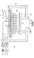
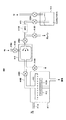
図16(A)は、このような本発明のプロセスを効率よく実行するのに適した、クラスタ型基板処理システム500の構成を、図16(B)は、前記基板システム500において実行される基板処理の流れを示す。
[第3実施例]
図17(A)は、本発明の第3実施例による基板処理システム600の構成を示す。ただし図17(A)中、先に説明した部分には同一の参照符号を付し、説明を省略する。
[第4実施例]
図18(A)は、本発明の第4実施例による基板処理システム700の構成を示す。ただし図18(A)中、先に説明した部分には同一の参照符号を付し、説明を省略する。
[第5実施例]
以上の説明では、図9(E)の低エネルギプラズマを使った前処理を、図5,6で説明したマイクロ波プラズマ処理装置10において行っているが、本発明はかかる特定のプラズマ処理装置に限定されるものではない。
[第6実施例]
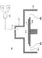
さらに図9(E)の前処理工程を、図20に示すリモートプラズマ源910を使った基板処理装置900にて行うことも可能である。
2 低誘電率膜
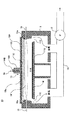
10,800,900 プラズマ処理装置
11 処理容器
11A プロセス空間
11B 基板保持台
11C 排気ポート
12 窓
12a シールリング(Oリング)
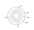
13 アンテナ本体
13A 導波部(シールド部材)
13B ラジアルラインスロットアンテナ
13a,13bスロット
13C 遅相板
14 同軸導波管
14A 外側導波管
14B 内側導体
15 ガス導入口
21,110 シリコン基板
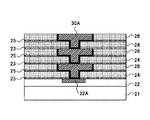
22,111 絶縁膜
22A,111A Cu配線パターン
22a,111Ox 酸化物
111x 銅残渣
23,25,27,112,114 エッチングストッパ膜
26,27,113,115 層間絶縁膜
26A,113A 配線溝
24A,113B ビアホール
28.116 バリアメタル膜
29 Cuシード層
30 Cu層
30A,117 Cu配線パターン
300 プラズマALD装置
301 処理容器
301a 処理容器上部
301b 処理容器底部
302 基板保持台
303 ヒータ
304 ヒータ電源
305 絶縁体
306,307,308,310 ガス通路
309,311 原料ガス吐出口
312 成膜原料源
313 Ar源
314 水素源
315 バルブ
316 MFC
317 整合器
318 高周波電源
319 排気口
320 排気装置
321 マッチャー
330 シャワーヘッド
400 CVD装置
411 処理容器
411A,416A 水素ガスライン
412 基板保持台
412A ヒータ
413 シャワーヘッド
414 Cu原料容器
415,416D 配管
415A,415C,416B,416C,416E バルブ
415B MFC
415D ドレイン
416 気化器
500,600,700 クラスタ型基板処理システム
501 導入側ウェハ搬送室(大気搬送室)
501A,501B カセットモジュール
501C ウェハオリエンタ
502A,502B ロードロック室
503,505 真空ウェハ搬送室
504A 脱ガス室
504B 前処理室
504C ALD室
504D ウェハ受け渡し室
506A CVD室
506B、506C PVD室
G1〜G9 ゲートバルブ
Claims (17)
- 層間絶縁膜中にビアホールを、前記層間絶縁膜の下に形成された低抵抗金属配線パターンが、前記ビアホールの底面において露出するように形成する工程と、
前記層間絶縁膜上に、前記ビアホールの側壁面および前記露出された低抵抗金属配線パターンを覆うように、前記ビアホールの形状に整合して導電性バリア膜を形成する工程と、
前記導電性バリア膜上に低抵抗金属膜を形成する工程と
よりなる半導体装置の製造方法であって、
前記ビアホール形成工程の後、前記導電性バリア膜の形成工程の前に、前記層間絶縁膜を、前記ビアホールの側壁面および前記ビアホールの底面を含めて、前記低抵抗金属パターンのスパッタが生じないようなエネルギの水素を含むプラズマで処理し、前記層間絶縁膜表面を、前記ビアホールの側壁面および前記ビアホールの底面を含めて水素終端する前処理工程を含むことを特徴とする半導体装置の製造方法。 - 前記前処理工程において前記プラズマの電子温度は、3eVを超えないことを特徴とする請求項1記載の半導体装置の製造方法。
- 前記前処理工程において前記プラズマは、マイクロ波により励起されることを特徴とする請求項または2記載の半導体装置の製造方法。
- 前記プラズマは、平面アンテナよりマイクロ波を放射することにより励起されることを特徴とする請求項1〜3のうち、いずれか一項記載の半導体装置の製造方法。
- 前記プラズマは、誘導コイルに供給される高周波により励起されることを特徴とする請求項1または2記載の半導体装置の製造方法。
- 前記プラズマは、リモートプラズマ源により形成されることを特徴とする請求項1記載の半導体装置の製造方法。
- 前記前処理工程において前記プラズマは、希ガスと、水素を含む還元ガスの混合ガスプラズマであることを特徴とする請求項1〜6のうち、いずれか一項記載の半導体装置の製造方法。
- 前記導電性バリア膜を形成する工程は、前記層間絶縁膜表面を、前記ビアホールの側壁面および底面を含めて導電性金属窒化物膜により覆う工程と、前記導電性金属窒化物膜を高融点金属膜で覆う工程とよりなることを特徴とする請求項1〜7のうち、いずれか一項記載の半導体装置の製造方法。
- 前記導電性金属窒化物膜を形成する工程は、前記層間絶縁膜表面を、前記ビアホールの側壁面および底面を含めて、窒素を含む有機金属原料分子で覆う第1の工程と、前記有機金属原料分子を分解する第2の工程とよりなり、前記第1の工程と前記第2の工程とは、間にパージ工程を挟みながら繰り返されることを特徴とする請求項1〜8のうち、いずれか一項記載の半導体装置の製造方法。
- 前記高融点金属膜を形成する工程は、前記導電性金属窒化物膜表面を、前記高融点金属膜を構成する高融点金属元素を含む金属原料分子で覆う第3の工程と、前記金属原料分子を分解する第4の工程とよりなり、前記第3の工程と前記第4の工程とは、間にパージ工程を挟みながら繰り返されることを特徴とする請求項9記載の半導体装置の製造方法。
- 前記層間絶縁膜は、プラズマCVD法により形成されたSiOCH膜であることを特徴とする請求項1〜10のうち、いずれか一項記載の半導体装置の製造方法。
- 前記層間絶縁膜は、無機SOD膜であることを特徴とする請求項1〜10のうち、いずれか一項記載の半導体装置の製造方法。
- 前記層間絶縁膜は、有機ポリマー膜であることを特徴とする請求項1〜10のうち、いずれか一項記載の半導体装置の製造方法。
- 前記層間絶縁膜は多孔質膜であることを特徴とする請求項1〜13のうち、いずれか一項記載の半導体装置の製造方法。
- 前記導電性バリア膜を形成する工程は第1の処理容器において実行され、前記低抵抗金属膜を形成する工程は前記第1の処理容器に真空搬送室により結合された第2の処理容器において実行されることを特徴とする請求項1〜14のうち、いずれか一項記載の半導体装置の製造方法。
- 前記前処理工程は第1の処理容器において実行され、前記導電性バリア膜を形成する工程は前記第1の処理容器に第1の真空搬送室を介して結合された第2の処理容器において実行され、
前記低抵抗金属膜を形成する工程は、前記第1の真空搬送室にゲートバルブを介して結合された第2の真空搬送室に結合された第3の処理容器において実行されることを特徴とする請求項1〜14のうち、いずれか一項記載の半導体装置の製造方法。 - 絶縁膜中に、前記絶縁膜の下に形成された金属パターンを、底面において露出するようにビアホールを形成する工程と、
前記絶縁膜上に、前記ビアホールの側壁面および前記露出された金属パターンを覆うように、前記ビアホールの形状に整合して導電性バリア膜を形成する工程と、
よりなる基板処理方法であって、
前記ビアホール形成工程の後、前記導電性バリア膜の形成工程の前に、前記絶縁膜を、前記ビアホールの側壁面および底面を含めて、前記金属パターンのスパッタが生じないようなエネルギの水素を含むプラズマで処理し、前記絶縁膜を、前記ビアホールの側壁面および底面を含めて水素終端する工程を含むことを特徴とする基板処理方法。
Priority Applications (3)
| Application Number | Priority Date | Filing Date | Title |
|---|---|---|---|
| JP2004164521A JP4503356B2 (ja) | 2004-06-02 | 2004-06-02 | 基板処理方法および半導体装置の製造方法 |
| US11/142,457 US7332426B2 (en) | 2004-06-02 | 2005-06-02 | Substrate processing method and fabrication process of a semiconductor device |
| US11/673,628 US7772111B2 (en) | 2004-06-02 | 2007-02-12 | Substrate processing method and fabrication process of a semiconductor device |
Applications Claiming Priority (1)
| Application Number | Priority Date | Filing Date | Title |
|---|---|---|---|
| JP2004164521A JP4503356B2 (ja) | 2004-06-02 | 2004-06-02 | 基板処理方法および半導体装置の製造方法 |
Publications (2)
| Publication Number | Publication Date |
|---|---|
| JP2005347472A true JP2005347472A (ja) | 2005-12-15 |
| JP4503356B2 JP4503356B2 (ja) | 2010-07-14 |
Family
ID=35449543
Family Applications (1)
| Application Number | Title | Priority Date | Filing Date |
|---|---|---|---|
| JP2004164521A Expired - Fee Related JP4503356B2 (ja) | 2004-06-02 | 2004-06-02 | 基板処理方法および半導体装置の製造方法 |
Country Status (2)
| Country | Link |
|---|---|
| US (2) | US7332426B2 (ja) |
| JP (1) | JP4503356B2 (ja) |
Cited By (10)
| Publication number | Priority date | Publication date | Assignee | Title |
|---|---|---|---|---|
| WO2007086126A1 (ja) * | 2006-01-26 | 2007-08-02 | Fujitsu Limited | 強誘電体メモリ装置およびその製造方法、半導体装置の製造方法 |
| WO2008146879A1 (ja) * | 2007-05-30 | 2008-12-04 | Tokyo Electron Limited | 半導体装置の製造方法、半導体製造装置及び記憶媒体 |
| WO2010059434A3 (en) * | 2008-11-19 | 2010-07-29 | Micron Technology, Inc. | Methods for forming a conductive material, methods for selectively forming a conductive material, methods for forming platinum, and methods for forming conductive structures |
| JP2010533987A (ja) * | 2007-07-20 | 2010-10-28 | アイメック | Iii−v族cmosデバイスでのダマシンコンタクト |
| US8598706B2 (en) | 2007-09-18 | 2013-12-03 | Renesas Electronics Corporation | Method for forming interlayer dielectric film, interlayer dielectric film, semiconductor device and semiconductor manufacturing apparatus |
| JP2014099627A (ja) * | 2006-08-30 | 2014-05-29 | Lam Research Corporation | 金属堆積のために基板表面を調整する方法および統合システム |
| US8999841B2 (en) | 2011-08-05 | 2015-04-07 | Tokyo Electron Limited | Semiconductor device manufacturing method |
| JP2015092548A (ja) * | 2013-09-16 | 2015-05-14 | エスピーティーエス テクノロジーズ リミティド | 半導体構造のプレクリーニング |
| US9576850B2 (en) | 2012-01-25 | 2017-02-21 | Tokyo Electron Limited | Method for manufacturing semiconductor device |
| US12538780B2 (en) | 2022-09-22 | 2026-01-27 | Kabushiki Kaisha Toshiba | Isolator |
Families Citing this family (325)
| Publication number | Priority date | Publication date | Assignee | Title |
|---|---|---|---|---|
| US20060226003A1 (en) * | 2003-01-22 | 2006-10-12 | John Mize | Apparatus and methods for ionized deposition of a film or thin layer |
| US20050178328A1 (en) * | 2004-02-17 | 2005-08-18 | Matsushita Electric Industrial Co., Ltd. | Film forming method and film forming apparatus |
| US7253125B1 (en) | 2004-04-16 | 2007-08-07 | Novellus Systems, Inc. | Method to improve mechanical strength of low-k dielectric film using modulated UV exposure |
| JP4503356B2 (ja) * | 2004-06-02 | 2010-07-14 | 東京エレクトロン株式会社 | 基板処理方法および半導体装置の製造方法 |
| US7605469B2 (en) * | 2004-06-30 | 2009-10-20 | Intel Corporation | Atomic layer deposited tantalum containing adhesion layer |
| US9659769B1 (en) | 2004-10-22 | 2017-05-23 | Novellus Systems, Inc. | Tensile dielectric films using UV curing |
| US7790633B1 (en) | 2004-10-26 | 2010-09-07 | Novellus Systems, Inc. | Sequential deposition/anneal film densification method |
| US7510982B1 (en) | 2005-01-31 | 2009-03-31 | Novellus Systems, Inc. | Creation of porosity in low-k films by photo-disassociation of imbedded nanoparticles |
| US9659758B2 (en) * | 2005-03-22 | 2017-05-23 | Honeywell International Inc. | Coils utilized in vapor deposition applications and methods of production |
| US8454750B1 (en) | 2005-04-26 | 2013-06-04 | Novellus Systems, Inc. | Multi-station sequential curing of dielectric films |
| US8282768B1 (en) | 2005-04-26 | 2012-10-09 | Novellus Systems, Inc. | Purging of porogen from UV cure chamber |
| US8889233B1 (en) | 2005-04-26 | 2014-11-18 | Novellus Systems, Inc. | Method for reducing stress in porous dielectric films |
| US8980769B1 (en) | 2005-04-26 | 2015-03-17 | Novellus Systems, Inc. | Multi-station sequential curing of dielectric films |
| US8137465B1 (en) | 2005-04-26 | 2012-03-20 | Novellus Systems, Inc. | Single-chamber sequential curing of semiconductor wafers |
| US20060278520A1 (en) * | 2005-06-13 | 2006-12-14 | Lee Eal H | Use of DC magnetron sputtering systems |
| US7704887B2 (en) * | 2005-11-22 | 2010-04-27 | Applied Materials, Inc. | Remote plasma pre-clean with low hydrogen pressure |
| JP5076482B2 (ja) * | 2006-01-20 | 2012-11-21 | 富士通セミコンダクター株式会社 | 半導体装置の製造方法 |
| US20080078325A1 (en) * | 2006-09-29 | 2008-04-03 | Tokyo Electron Limited | Processing system containing a hot filament hydrogen radical source for integrated substrate processing |
| US20080081464A1 (en) * | 2006-09-29 | 2008-04-03 | Tokyo Electron Limited | Method of integrated substrated processing using a hot filament hydrogen radical souce |
| JP2008091645A (ja) * | 2006-10-02 | 2008-04-17 | Tokyo Electron Ltd | 半導体製造装置、半導体装置の製造方法及び記憶媒体 |
| US8465991B2 (en) | 2006-10-30 | 2013-06-18 | Novellus Systems, Inc. | Carbon containing low-k dielectric constant recovery using UV treatment |
| US7851232B2 (en) | 2006-10-30 | 2010-12-14 | Novellus Systems, Inc. | UV treatment for carbon-containing low-k dielectric repair in semiconductor processing |
| US10037905B2 (en) | 2009-11-12 | 2018-07-31 | Novellus Systems, Inc. | UV and reducing treatment for K recovery and surface clean in semiconductor processing |
| US7906174B1 (en) | 2006-12-07 | 2011-03-15 | Novellus Systems, Inc. | PECVD methods for producing ultra low-k dielectric films using UV treatment |
| US8242028B1 (en) | 2007-04-03 | 2012-08-14 | Novellus Systems, Inc. | UV treatment of etch stop and hard mask films for selectivity and hermeticity enhancement |
| US20080254619A1 (en) * | 2007-04-14 | 2008-10-16 | Tsang-Jung Lin | Method of fabricating a semiconductor device |
| US8211510B1 (en) | 2007-08-31 | 2012-07-03 | Novellus Systems, Inc. | Cascaded cure approach to fabricate highly tensile silicon nitride films |
| US20090194414A1 (en) * | 2008-01-31 | 2009-08-06 | Nolander Ira G | Modified sputtering target and deposition components, methods of production and uses thereof |
| US20090218692A1 (en) * | 2008-02-29 | 2009-09-03 | Roland Hampp | Barrier for Copper Integration in the FEOL |
| US20090258487A1 (en) * | 2008-04-14 | 2009-10-15 | Keng-Chu Lin | Method for Improving the Reliability of Low-k Dielectric Materials |
| KR101525805B1 (ko) * | 2008-06-11 | 2015-06-05 | 삼성디스플레이 주식회사 | 표시 장치 및 그 제조 방법 |
| US9050623B1 (en) | 2008-09-12 | 2015-06-09 | Novellus Systems, Inc. | Progressive UV cure |
| US20100308380A1 (en) * | 2009-06-05 | 2010-12-09 | International Business Machines Corporation | Dual damascene processing for gate conductor and active area to first metal level interconnect structures |
| US8168528B2 (en) * | 2009-06-18 | 2012-05-01 | Kabushiki Kaisha Toshiba | Restoration method using metal for better CD controllability and Cu filing |
| JP5507909B2 (ja) * | 2009-07-14 | 2014-05-28 | 東京エレクトロン株式会社 | 成膜方法 |
| US20130344702A1 (en) * | 2011-03-04 | 2013-12-26 | Tokyo Electron Limited | Method of etching silicon nitride films |
| US20130023129A1 (en) | 2011-07-20 | 2013-01-24 | Asm America, Inc. | Pressure transmitter for a semiconductor processing environment |
| US10714315B2 (en) | 2012-10-12 | 2020-07-14 | Asm Ip Holdings B.V. | Semiconductor reaction chamber showerhead |
| US20160376700A1 (en) | 2013-02-01 | 2016-12-29 | Asm Ip Holding B.V. | System for treatment of deposition reactor |
| JP6338462B2 (ja) * | 2013-09-11 | 2018-06-06 | 東京エレクトロン株式会社 | プラズマ処理装置 |
| US11015245B2 (en) | 2014-03-19 | 2021-05-25 | Asm Ip Holding B.V. | Gas-phase reactor and system having exhaust plenum and components thereof |
| US10858737B2 (en) | 2014-07-28 | 2020-12-08 | Asm Ip Holding B.V. | Showerhead assembly and components thereof |
| US10941490B2 (en) | 2014-10-07 | 2021-03-09 | Asm Ip Holding B.V. | Multiple temperature range susceptor, assembly, reactor and system including the susceptor, and methods of using the same |
| JP6404111B2 (ja) * | 2014-12-18 | 2018-10-10 | 東京エレクトロン株式会社 | プラズマ処理装置 |
| JP2016167545A (ja) * | 2015-03-10 | 2016-09-15 | 東京エレクトロン株式会社 | ビアホール底のクリーニング方法および半導体装置の製造方法 |
| US10276355B2 (en) | 2015-03-12 | 2019-04-30 | Asm Ip Holding B.V. | Multi-zone reactor, system including the reactor, and method of using the same |
| US10458018B2 (en) | 2015-06-26 | 2019-10-29 | Asm Ip Holding B.V. | Structures including metal carbide material, devices including the structures, and methods of forming same |
| CN106505030B (zh) * | 2015-09-06 | 2019-07-26 | 中芯国际集成电路制造(上海)有限公司 | 硅通孔结构的制备方法 |
| US9887160B2 (en) * | 2015-09-24 | 2018-02-06 | International Business Machines Corporation | Multiple pre-clean processes for interconnect fabrication |
| US10211308B2 (en) | 2015-10-21 | 2019-02-19 | Asm Ip Holding B.V. | NbMC layers |
| US11139308B2 (en) | 2015-12-29 | 2021-10-05 | Asm Ip Holding B.V. | Atomic layer deposition of III-V compounds to form V-NAND devices |
| US10529554B2 (en) | 2016-02-19 | 2020-01-07 | Asm Ip Holding B.V. | Method for forming silicon nitride film selectively on sidewalls or flat surfaces of trenches |
| US10343920B2 (en) | 2016-03-18 | 2019-07-09 | Asm Ip Holding B.V. | Aligned carbon nanotubes |
| US10367080B2 (en) | 2016-05-02 | 2019-07-30 | Asm Ip Holding B.V. | Method of forming a germanium oxynitride film |
| US11453943B2 (en) | 2016-05-25 | 2022-09-27 | Asm Ip Holding B.V. | Method for forming carbon-containing silicon/metal oxide or nitride film by ALD using silicon precursor and hydrocarbon precursor |
| US10612137B2 (en) | 2016-07-08 | 2020-04-07 | Asm Ip Holdings B.V. | Organic reactants for atomic layer deposition |
| US9859151B1 (en) | 2016-07-08 | 2018-01-02 | Asm Ip Holding B.V. | Selective film deposition method to form air gaps |
| US9887082B1 (en) | 2016-07-28 | 2018-02-06 | Asm Ip Holding B.V. | Method and apparatus for filling a gap |
| US9812320B1 (en) | 2016-07-28 | 2017-11-07 | Asm Ip Holding B.V. | Method and apparatus for filling a gap |
| KR102532607B1 (ko) | 2016-07-28 | 2023-05-15 | 에이에스엠 아이피 홀딩 비.브이. | 기판 가공 장치 및 그 동작 방법 |
| US9847221B1 (en) | 2016-09-29 | 2017-12-19 | Lam Research Corporation | Low temperature formation of high quality silicon oxide films in semiconductor device manufacturing |
| US11532757B2 (en) | 2016-10-27 | 2022-12-20 | Asm Ip Holding B.V. | Deposition of charge trapping layers |
| US10714350B2 (en) | 2016-11-01 | 2020-07-14 | ASM IP Holdings, B.V. | Methods for forming a transition metal niobium nitride film on a substrate by atomic layer deposition and related semiconductor device structures |
| KR102546317B1 (ko) | 2016-11-15 | 2023-06-21 | 에이에스엠 아이피 홀딩 비.브이. | 기체 공급 유닛 및 이를 포함하는 기판 처리 장치 |
| KR102762543B1 (ko) | 2016-12-14 | 2025-02-05 | 에이에스엠 아이피 홀딩 비.브이. | 기판 처리 장치 |
| US11581186B2 (en) | 2016-12-15 | 2023-02-14 | Asm Ip Holding B.V. | Sequential infiltration synthesis apparatus |
| US11447861B2 (en) | 2016-12-15 | 2022-09-20 | Asm Ip Holding B.V. | Sequential infiltration synthesis apparatus and a method of forming a patterned structure |
| KR102700194B1 (ko) | 2016-12-19 | 2024-08-28 | 에이에스엠 아이피 홀딩 비.브이. | 기판 처리 장치 |
| CN106654523A (zh) * | 2016-12-20 | 2017-05-10 | 西安科锐盛创新科技有限公司 | 用于可重构多层全息天线的Si基SPiN二极管制备方法 |
| CN106654522A (zh) * | 2016-12-20 | 2017-05-10 | 西安科锐盛创新科技有限公司 | 一种多层全息天线SiGe基等离子pin二极管的制备方法 |
| US10269558B2 (en) | 2016-12-22 | 2019-04-23 | Asm Ip Holding B.V. | Method of forming a structure on a substrate |
| US11390950B2 (en) | 2017-01-10 | 2022-07-19 | Asm Ip Holding B.V. | Reactor system and method to reduce residue buildup during a film deposition process |
| US10468261B2 (en) | 2017-02-15 | 2019-11-05 | Asm Ip Holding B.V. | Methods for forming a metallic film on a substrate by cyclical deposition and related semiconductor device structures |
| US10529563B2 (en) | 2017-03-29 | 2020-01-07 | Asm Ip Holdings B.V. | Method for forming doped metal oxide films on a substrate by cyclical deposition and related semiconductor device structures |
| US10770286B2 (en) | 2017-05-08 | 2020-09-08 | Asm Ip Holdings B.V. | Methods for selectively forming a silicon nitride film on a substrate and related semiconductor device structures |
| US12040200B2 (en) | 2017-06-20 | 2024-07-16 | Asm Ip Holding B.V. | Semiconductor processing apparatus and methods for calibrating a semiconductor processing apparatus |
| US11306395B2 (en) | 2017-06-28 | 2022-04-19 | Asm Ip Holding B.V. | Methods for depositing a transition metal nitride film on a substrate by atomic layer deposition and related deposition apparatus |
| KR20190009245A (ko) | 2017-07-18 | 2019-01-28 | 에이에스엠 아이피 홀딩 비.브이. | 반도체 소자 구조물 형성 방법 및 관련된 반도체 소자 구조물 |
| US11374112B2 (en) | 2017-07-19 | 2022-06-28 | Asm Ip Holding B.V. | Method for depositing a group IV semiconductor and related semiconductor device structures |
| US11018002B2 (en) | 2017-07-19 | 2021-05-25 | Asm Ip Holding B.V. | Method for selectively depositing a Group IV semiconductor and related semiconductor device structures |
| US10541333B2 (en) | 2017-07-19 | 2020-01-21 | Asm Ip Holding B.V. | Method for depositing a group IV semiconductor and related semiconductor device structures |
| US10590535B2 (en) | 2017-07-26 | 2020-03-17 | Asm Ip Holdings B.V. | Chemical treatment, deposition and/or infiltration apparatus and method for using the same |
| TWI815813B (zh) | 2017-08-04 | 2023-09-21 | 荷蘭商Asm智慧財產控股公司 | 用於分配反應腔內氣體的噴頭總成 |
| US10692741B2 (en) | 2017-08-08 | 2020-06-23 | Asm Ip Holdings B.V. | Radiation shield |
| US10770336B2 (en) | 2017-08-08 | 2020-09-08 | Asm Ip Holding B.V. | Substrate lift mechanism and reactor including same |
| US11769682B2 (en) | 2017-08-09 | 2023-09-26 | Asm Ip Holding B.V. | Storage apparatus for storing cassettes for substrates and processing apparatus equipped therewith |
| US11139191B2 (en) | 2017-08-09 | 2021-10-05 | Asm Ip Holding B.V. | Storage apparatus for storing cassettes for substrates and processing apparatus equipped therewith |
| US11830730B2 (en) | 2017-08-29 | 2023-11-28 | Asm Ip Holding B.V. | Layer forming method and apparatus |
| KR102491945B1 (ko) | 2017-08-30 | 2023-01-26 | 에이에스엠 아이피 홀딩 비.브이. | 기판 처리 장치 |
| US11295980B2 (en) | 2017-08-30 | 2022-04-05 | Asm Ip Holding B.V. | Methods for depositing a molybdenum metal film over a dielectric surface of a substrate by a cyclical deposition process and related semiconductor device structures |
| US11056344B2 (en) | 2017-08-30 | 2021-07-06 | Asm Ip Holding B.V. | Layer forming method |
| US10658205B2 (en) | 2017-09-28 | 2020-05-19 | Asm Ip Holdings B.V. | Chemical dispensing apparatus and methods for dispensing a chemical to a reaction chamber |
| US10403504B2 (en) | 2017-10-05 | 2019-09-03 | Asm Ip Holding B.V. | Method for selectively depositing a metallic film on a substrate |
| US11183373B2 (en) | 2017-10-11 | 2021-11-23 | Honeywell International Inc. | Multi-patterned sputter traps and methods of making |
| US10923344B2 (en) | 2017-10-30 | 2021-02-16 | Asm Ip Holding B.V. | Methods for forming a semiconductor structure and related semiconductor structures |
| US11022879B2 (en) | 2017-11-24 | 2021-06-01 | Asm Ip Holding B.V. | Method of forming an enhanced unexposed photoresist layer |
| JP7214724B2 (ja) | 2017-11-27 | 2023-01-30 | エーエスエム アイピー ホールディング ビー.ブイ. | バッチ炉で利用されるウェハカセットを収納するための収納装置 |
| TWI791689B (zh) | 2017-11-27 | 2023-02-11 | 荷蘭商Asm智慧財產控股私人有限公司 | 包括潔淨迷你環境之裝置 |
| US10872771B2 (en) | 2018-01-16 | 2020-12-22 | Asm Ip Holding B. V. | Method for depositing a material film on a substrate within a reaction chamber by a cyclical deposition process and related device structures |
| KR102695659B1 (ko) | 2018-01-19 | 2024-08-14 | 에이에스엠 아이피 홀딩 비.브이. | 플라즈마 보조 증착에 의해 갭 충진 층을 증착하는 방법 |
| TWI799494B (zh) | 2018-01-19 | 2023-04-21 | 荷蘭商Asm 智慧財產控股公司 | 沈積方法 |
| US11081345B2 (en) | 2018-02-06 | 2021-08-03 | Asm Ip Holding B.V. | Method of post-deposition treatment for silicon oxide film |
| US10896820B2 (en) | 2018-02-14 | 2021-01-19 | Asm Ip Holding B.V. | Method for depositing a ruthenium-containing film on a substrate by a cyclical deposition process |
| US11685991B2 (en) | 2018-02-14 | 2023-06-27 | Asm Ip Holding B.V. | Method for depositing a ruthenium-containing film on a substrate by a cyclical deposition process |
| US10731249B2 (en) | 2018-02-15 | 2020-08-04 | Asm Ip Holding B.V. | Method of forming a transition metal containing film on a substrate by a cyclical deposition process, a method for supplying a transition metal halide compound to a reaction chamber, and related vapor deposition apparatus |
| KR102636427B1 (ko) | 2018-02-20 | 2024-02-13 | 에이에스엠 아이피 홀딩 비.브이. | 기판 처리 방법 및 장치 |
| US10975470B2 (en) | 2018-02-23 | 2021-04-13 | Asm Ip Holding B.V. | Apparatus for detecting or monitoring for a chemical precursor in a high temperature environment |
| US11473195B2 (en) | 2018-03-01 | 2022-10-18 | Asm Ip Holding B.V. | Semiconductor processing apparatus and a method for processing a substrate |
| US11629406B2 (en) | 2018-03-09 | 2023-04-18 | Asm Ip Holding B.V. | Semiconductor processing apparatus comprising one or more pyrometers for measuring a temperature of a substrate during transfer of the substrate |
| US11114283B2 (en) | 2018-03-16 | 2021-09-07 | Asm Ip Holding B.V. | Reactor, system including the reactor, and methods of manufacturing and using same |
| KR102646467B1 (ko) | 2018-03-27 | 2024-03-11 | 에이에스엠 아이피 홀딩 비.브이. | 기판 상에 전극을 형성하는 방법 및 전극을 포함하는 반도체 소자 구조 |
| US11230766B2 (en) | 2018-03-29 | 2022-01-25 | Asm Ip Holding B.V. | Substrate processing apparatus and method |
| US11088002B2 (en) | 2018-03-29 | 2021-08-10 | Asm Ip Holding B.V. | Substrate rack and a substrate processing system and method |
| KR102600229B1 (ko) | 2018-04-09 | 2023-11-10 | 에이에스엠 아이피 홀딩 비.브이. | 기판 지지 장치, 이를 포함하는 기판 처리 장치 및 기판 처리 방법 |
| TWI843623B (zh) | 2018-05-08 | 2024-05-21 | 荷蘭商Asm Ip私人控股有限公司 | 藉由循環沉積製程於基板上沉積氧化物膜之方法及相關裝置結構 |
| US12025484B2 (en) | 2018-05-08 | 2024-07-02 | Asm Ip Holding B.V. | Thin film forming method |
| US12272527B2 (en) | 2018-05-09 | 2025-04-08 | Asm Ip Holding B.V. | Apparatus for use with hydrogen radicals and method of using same |
| KR102596988B1 (ko) | 2018-05-28 | 2023-10-31 | 에이에스엠 아이피 홀딩 비.브이. | 기판 처리 방법 및 그에 의해 제조된 장치 |
| US11718913B2 (en) | 2018-06-04 | 2023-08-08 | Asm Ip Holding B.V. | Gas distribution system and reactor system including same |
| TWI840362B (zh) | 2018-06-04 | 2024-05-01 | 荷蘭商Asm Ip私人控股有限公司 | 水氣降低的晶圓處置腔室 |
| US11286562B2 (en) | 2018-06-08 | 2022-03-29 | Asm Ip Holding B.V. | Gas-phase chemical reactor and method of using same |
| KR102568797B1 (ko) | 2018-06-21 | 2023-08-21 | 에이에스엠 아이피 홀딩 비.브이. | 기판 처리 시스템 |
| US10797133B2 (en) | 2018-06-21 | 2020-10-06 | Asm Ip Holding B.V. | Method for depositing a phosphorus doped silicon arsenide film and related semiconductor device structures |
| TWI871083B (zh) | 2018-06-27 | 2025-01-21 | 荷蘭商Asm Ip私人控股有限公司 | 用於形成含金屬材料之循環沉積製程 |
| US11499222B2 (en) | 2018-06-27 | 2022-11-15 | Asm Ip Holding B.V. | Cyclic deposition methods for forming metal-containing material and films and structures including the metal-containing material |
| US10612136B2 (en) | 2018-06-29 | 2020-04-07 | ASM IP Holding, B.V. | Temperature-controlled flange and reactor system including same |
| US10755922B2 (en) | 2018-07-03 | 2020-08-25 | Asm Ip Holding B.V. | Method for depositing silicon-free carbon-containing film as gap-fill layer by pulse plasma-assisted deposition |
| US10388513B1 (en) | 2018-07-03 | 2019-08-20 | Asm Ip Holding B.V. | Method for depositing silicon-free carbon-containing film as gap-fill layer by pulse plasma-assisted deposition |
| US11053591B2 (en) | 2018-08-06 | 2021-07-06 | Asm Ip Holding B.V. | Multi-port gas injection system and reactor system including same |
| US11430674B2 (en) | 2018-08-22 | 2022-08-30 | Asm Ip Holding B.V. | Sensor array, apparatus for dispensing a vapor phase reactant to a reaction chamber and related methods |
| US11024523B2 (en) | 2018-09-11 | 2021-06-01 | Asm Ip Holding B.V. | Substrate processing apparatus and method |
| KR102707956B1 (ko) | 2018-09-11 | 2024-09-19 | 에이에스엠 아이피 홀딩 비.브이. | 박막 증착 방법 |
| US11049751B2 (en) | 2018-09-14 | 2021-06-29 | Asm Ip Holding B.V. | Cassette supply system to store and handle cassettes and processing apparatus equipped therewith |
| CN110970344B (zh) | 2018-10-01 | 2024-10-25 | Asmip控股有限公司 | 衬底保持设备、包含所述设备的系统及其使用方法 |
| US11232963B2 (en) | 2018-10-03 | 2022-01-25 | Asm Ip Holding B.V. | Substrate processing apparatus and method |
| KR102592699B1 (ko) | 2018-10-08 | 2023-10-23 | 에이에스엠 아이피 홀딩 비.브이. | 기판 지지 유닛 및 이를 포함하는 박막 증착 장치와 기판 처리 장치 |
| KR102546322B1 (ko) | 2018-10-19 | 2023-06-21 | 에이에스엠 아이피 홀딩 비.브이. | 기판 처리 장치 및 기판 처리 방법 |
| KR102605121B1 (ko) | 2018-10-19 | 2023-11-23 | 에이에스엠 아이피 홀딩 비.브이. | 기판 처리 장치 및 기판 처리 방법 |
| USD948463S1 (en) | 2018-10-24 | 2022-04-12 | Asm Ip Holding B.V. | Susceptor for semiconductor substrate supporting apparatus |
| US12378665B2 (en) | 2018-10-26 | 2025-08-05 | Asm Ip Holding B.V. | High temperature coatings for a preclean and etch apparatus and related methods |
| US11087997B2 (en) | 2018-10-31 | 2021-08-10 | Asm Ip Holding B.V. | Substrate processing apparatus for processing substrates |
| KR102748291B1 (ko) | 2018-11-02 | 2024-12-31 | 에이에스엠 아이피 홀딩 비.브이. | 기판 지지 유닛 및 이를 포함하는 기판 처리 장치 |
| US11572620B2 (en) | 2018-11-06 | 2023-02-07 | Asm Ip Holding B.V. | Methods for selectively depositing an amorphous silicon film on a substrate |
| US11031242B2 (en) | 2018-11-07 | 2021-06-08 | Asm Ip Holding B.V. | Methods for depositing a boron doped silicon germanium film |
| US10818758B2 (en) | 2018-11-16 | 2020-10-27 | Asm Ip Holding B.V. | Methods for forming a metal silicate film on a substrate in a reaction chamber and related semiconductor device structures |
| US10847366B2 (en) | 2018-11-16 | 2020-11-24 | Asm Ip Holding B.V. | Methods for depositing a transition metal chalcogenide film on a substrate by a cyclical deposition process |
| US12040199B2 (en) | 2018-11-28 | 2024-07-16 | Asm Ip Holding B.V. | Substrate processing apparatus for processing substrates |
| US11217444B2 (en) | 2018-11-30 | 2022-01-04 | Asm Ip Holding B.V. | Method for forming an ultraviolet radiation responsive metal oxide-containing film |
| KR102636428B1 (ko) | 2018-12-04 | 2024-02-13 | 에이에스엠 아이피 홀딩 비.브이. | 기판 처리 장치를 세정하는 방법 |
| US11158513B2 (en) | 2018-12-13 | 2021-10-26 | Asm Ip Holding B.V. | Methods for forming a rhenium-containing film on a substrate by a cyclical deposition process and related semiconductor device structures |
| JP7504584B2 (ja) | 2018-12-14 | 2024-06-24 | エーエスエム・アイピー・ホールディング・ベー・フェー | 窒化ガリウムの選択的堆積を用いてデバイス構造体を形成する方法及びそのためのシステム |
| TWI866480B (zh) | 2019-01-17 | 2024-12-11 | 荷蘭商Asm Ip 私人控股有限公司 | 藉由循環沈積製程於基板上形成含過渡金屬膜之方法 |
| KR102727227B1 (ko) | 2019-01-22 | 2024-11-07 | 에이에스엠 아이피 홀딩 비.브이. | 기판 처리 장치 |
| CN111524788B (zh) | 2019-02-01 | 2023-11-24 | Asm Ip私人控股有限公司 | 氧化硅的拓扑选择性膜形成的方法 |
| TWI845607B (zh) | 2019-02-20 | 2024-06-21 | 荷蘭商Asm Ip私人控股有限公司 | 用來填充形成於基材表面內之凹部的循環沉積方法及設備 |
| KR102626263B1 (ko) | 2019-02-20 | 2024-01-16 | 에이에스엠 아이피 홀딩 비.브이. | 처리 단계를 포함하는 주기적 증착 방법 및 이를 위한 장치 |
| TWI873122B (zh) | 2019-02-20 | 2025-02-21 | 荷蘭商Asm Ip私人控股有限公司 | 填充一基板之一表面內所形成的一凹槽的方法、根據其所形成之半導體結構、及半導體處理設備 |
| KR20200102357A (ko) | 2019-02-20 | 2020-08-31 | 에이에스엠 아이피 홀딩 비.브이. | 3-d nand 응용의 플러그 충진체 증착용 장치 및 방법 |
| TWI842826B (zh) | 2019-02-22 | 2024-05-21 | 荷蘭商Asm Ip私人控股有限公司 | 基材處理設備及處理基材之方法 |
| KR102762833B1 (ko) | 2019-03-08 | 2025-02-04 | 에이에스엠 아이피 홀딩 비.브이. | SiOCN 층을 포함한 구조체 및 이의 형성 방법 |
| KR102858005B1 (ko) | 2019-03-08 | 2025-09-09 | 에이에스엠 아이피 홀딩 비.브이. | 실리콘 질화물 층을 선택적으로 증착하는 방법, 및 선택적으로 증착된 실리콘 질화물 층을 포함하는 구조체 |
| KR102782593B1 (ko) | 2019-03-08 | 2025-03-14 | 에이에스엠 아이피 홀딩 비.브이. | SiOC 층을 포함한 구조체 및 이의 형성 방법 |
| JP2020167398A (ja) | 2019-03-28 | 2020-10-08 | エーエスエム・アイピー・ホールディング・ベー・フェー | ドアオープナーおよびドアオープナーが提供される基材処理装置 |
| KR102809999B1 (ko) | 2019-04-01 | 2025-05-19 | 에이에스엠 아이피 홀딩 비.브이. | 반도체 소자를 제조하는 방법 |
| KR102897355B1 (ko) | 2019-04-19 | 2025-12-08 | 에이에스엠 아이피 홀딩 비.브이. | 층 형성 방법 및 장치 |
| KR20200125453A (ko) | 2019-04-24 | 2020-11-04 | 에이에스엠 아이피 홀딩 비.브이. | 기상 반응기 시스템 및 이를 사용하는 방법 |
| KR102869364B1 (ko) | 2019-05-07 | 2025-10-10 | 에이에스엠 아이피 홀딩 비.브이. | 비정질 탄소 중합체 막을 개질하는 방법 |
| KR102929471B1 (ko) | 2019-05-07 | 2026-02-20 | 에이에스엠 아이피 홀딩 비.브이. | 딥 튜브가 있는 화학물질 공급원 용기 |
| KR102929472B1 (ko) | 2019-05-10 | 2026-02-20 | 에이에스엠 아이피 홀딩 비.브이. | 표면 상에 재료를 증착하는 방법 및 본 방법에 따라 형성된 구조 |
| JP7612342B2 (ja) | 2019-05-16 | 2025-01-14 | エーエスエム・アイピー・ホールディング・ベー・フェー | ウェハボートハンドリング装置、縦型バッチ炉および方法 |
| JP7598201B2 (ja) | 2019-05-16 | 2024-12-11 | エーエスエム・アイピー・ホールディング・ベー・フェー | ウェハボートハンドリング装置、縦型バッチ炉および方法 |
| USD947913S1 (en) | 2019-05-17 | 2022-04-05 | Asm Ip Holding B.V. | Susceptor shaft |
| USD975665S1 (en) | 2019-05-17 | 2023-01-17 | Asm Ip Holding B.V. | Susceptor shaft |
| USD935572S1 (en) | 2019-05-24 | 2021-11-09 | Asm Ip Holding B.V. | Gas channel plate |
| USD922229S1 (en) | 2019-06-05 | 2021-06-15 | Asm Ip Holding B.V. | Device for controlling a temperature of a gas supply unit |
| KR20200141002A (ko) | 2019-06-06 | 2020-12-17 | 에이에스엠 아이피 홀딩 비.브이. | 배기 가스 분석을 포함한 기상 반응기 시스템을 사용하는 방법 |
| KR102918757B1 (ko) | 2019-06-10 | 2026-01-28 | 에이에스엠 아이피 홀딩 비.브이. | 석영 에피택셜 챔버를 세정하는 방법 |
| KR20200143254A (ko) | 2019-06-11 | 2020-12-23 | 에이에스엠 아이피 홀딩 비.브이. | 개질 가스를 사용하여 전자 구조를 형성하는 방법, 상기 방법을 수행하기 위한 시스템, 및 상기 방법을 사용하여 형성되는 구조 |
| USD944946S1 (en) | 2019-06-14 | 2022-03-01 | Asm Ip Holding B.V. | Shower plate |
| USD931978S1 (en) | 2019-06-27 | 2021-09-28 | Asm Ip Holding B.V. | Showerhead vacuum transport |
| KR102911421B1 (ko) | 2019-07-03 | 2026-01-12 | 에이에스엠 아이피 홀딩 비.브이. | 기판 처리 장치용 온도 제어 조립체 및 이를 사용하는 방법 |
| JP7499079B2 (ja) | 2019-07-09 | 2024-06-13 | エーエスエム・アイピー・ホールディング・ベー・フェー | 同軸導波管を用いたプラズマ装置、基板処理方法 |
| CN112216646B (zh) | 2019-07-10 | 2026-02-10 | Asmip私人控股有限公司 | 基板支撑组件及包括其的基板处理装置 |
| KR102895115B1 (ko) | 2019-07-16 | 2025-12-03 | 에이에스엠 아이피 홀딩 비.브이. | 기판 처리 장치 |
| KR102860110B1 (ko) | 2019-07-17 | 2025-09-16 | 에이에스엠 아이피 홀딩 비.브이. | 실리콘 게르마늄 구조를 형성하는 방법 |
| TWI826704B (zh) | 2019-07-17 | 2023-12-21 | 荷蘭商Asm Ip私人控股有限公司 | 自由基輔助引燃電漿系統和方法 |
| US11643724B2 (en) | 2019-07-18 | 2023-05-09 | Asm Ip Holding B.V. | Method of forming structures using a neutral beam |
| KR102903090B1 (ko) | 2019-07-19 | 2025-12-19 | 에이에스엠 아이피 홀딩 비.브이. | 토폴로지-제어된 비정질 탄소 중합체 막을 형성하는 방법 |
| TWI839544B (zh) | 2019-07-19 | 2024-04-21 | 荷蘭商Asm Ip私人控股有限公司 | 形成形貌受控的非晶碳聚合物膜之方法 |
| CN112309843B (zh) | 2019-07-29 | 2026-01-23 | Asmip私人控股有限公司 | 实现高掺杂剂掺入的选择性沉积方法 |
| KR20210015655A (ko) | 2019-07-30 | 2021-02-10 | 에이에스엠 아이피 홀딩 비.브이. | 기판 처리 장치 및 방법 |
| CN112309900B (zh) | 2019-07-30 | 2025-11-04 | Asmip私人控股有限公司 | 基板处理设备 |
| CN112309899B (zh) | 2019-07-30 | 2025-11-14 | Asmip私人控股有限公司 | 基板处理设备 |
| US11227782B2 (en) | 2019-07-31 | 2022-01-18 | Asm Ip Holding B.V. | Vertical batch furnace assembly |
| US11587815B2 (en) | 2019-07-31 | 2023-02-21 | Asm Ip Holding B.V. | Vertical batch furnace assembly |
| US11587814B2 (en) | 2019-07-31 | 2023-02-21 | Asm Ip Holding B.V. | Vertical batch furnace assembly |
| KR20210018759A (ko) | 2019-08-05 | 2021-02-18 | 에이에스엠 아이피 홀딩 비.브이. | 화학물질 공급원 용기를 위한 액체 레벨 센서 |
| KR20210018761A (ko) | 2019-08-09 | 2021-02-18 | 에이에스엠 아이피 홀딩 비.브이. | 냉각 장치를 포함한 히터 어셈블리 및 이를 사용하는 방법 |
| USD965524S1 (en) | 2019-08-19 | 2022-10-04 | Asm Ip Holding B.V. | Susceptor support |
| USD965044S1 (en) | 2019-08-19 | 2022-09-27 | Asm Ip Holding B.V. | Susceptor shaft |
| JP7810514B2 (ja) | 2019-08-21 | 2026-02-03 | エーエスエム・アイピー・ホールディング・ベー・フェー | 成膜原料混合ガス生成装置及び成膜装置 |
| USD930782S1 (en) | 2019-08-22 | 2021-09-14 | Asm Ip Holding B.V. | Gas distributor |
| USD949319S1 (en) | 2019-08-22 | 2022-04-19 | Asm Ip Holding B.V. | Exhaust duct |
| USD940837S1 (en) | 2019-08-22 | 2022-01-11 | Asm Ip Holding B.V. | Electrode |
| USD979506S1 (en) | 2019-08-22 | 2023-02-28 | Asm Ip Holding B.V. | Insulator |
| KR20210024423A (ko) | 2019-08-22 | 2021-03-05 | 에이에스엠 아이피 홀딩 비.브이. | 홀을 구비한 구조체를 형성하기 위한 방법 |
| US11286558B2 (en) | 2019-08-23 | 2022-03-29 | Asm Ip Holding B.V. | Methods for depositing a molybdenum nitride film on a surface of a substrate by a cyclical deposition process and related semiconductor device structures including a molybdenum nitride film |
| KR102928101B1 (ko) | 2019-08-23 | 2026-02-13 | 에이에스엠 아이피 홀딩 비.브이. | 비스(디에틸아미노)실란을 사용하여 peald에 의해 개선된 품질을 갖는 실리콘 산화물 막을 증착하기 위한 방법 |
| KR102868968B1 (ko) | 2019-09-03 | 2025-10-10 | 에이에스엠 아이피 홀딩 비.브이. | 칼코지나이드 막 및 상기 막을 포함한 구조체를 증착하기 위한 방법 및 장치 |
| KR102806450B1 (ko) | 2019-09-04 | 2025-05-12 | 에이에스엠 아이피 홀딩 비.브이. | 희생 캡핑 층을 이용한 선택적 증착 방법 |
| KR102733104B1 (ko) | 2019-09-05 | 2024-11-22 | 에이에스엠 아이피 홀딩 비.브이. | 기판 처리 장치 |
| US12469693B2 (en) | 2019-09-17 | 2025-11-11 | Asm Ip Holding B.V. | Method of forming a carbon-containing layer and structure including the layer |
| US11562901B2 (en) | 2019-09-25 | 2023-01-24 | Asm Ip Holding B.V. | Substrate processing method |
| CN112593212B (zh) | 2019-10-02 | 2023-12-22 | Asm Ip私人控股有限公司 | 通过循环等离子体增强沉积工艺形成拓扑选择性氧化硅膜的方法 |
| TWI846953B (zh) | 2019-10-08 | 2024-07-01 | 荷蘭商Asm Ip私人控股有限公司 | 基板處理裝置 |
| KR102948143B1 (ko) | 2019-10-08 | 2026-04-07 | 에이에스엠 아이피 홀딩 비.브이. | 활성 종을 이용하기 위한 가스 분배 어셈블리를 포함한 반응기 시스템 및 이를 사용하는 방법 |
| TW202128273A (zh) | 2019-10-08 | 2021-08-01 | 荷蘭商Asm Ip私人控股有限公司 | 氣體注入系統、及將材料沉積於反應室內之基板表面上的方法 |
| TWI846966B (zh) | 2019-10-10 | 2024-07-01 | 荷蘭商Asm Ip私人控股有限公司 | 形成光阻底層之方法及包括光阻底層之結構 |
| US12009241B2 (en) | 2019-10-14 | 2024-06-11 | Asm Ip Holding B.V. | Vertical batch furnace assembly with detector to detect cassette |
| TWI834919B (zh) | 2019-10-16 | 2024-03-11 | 荷蘭商Asm Ip私人控股有限公司 | 氧化矽之拓撲選擇性膜形成之方法 |
| US11637014B2 (en) | 2019-10-17 | 2023-04-25 | Asm Ip Holding B.V. | Methods for selective deposition of doped semiconductor material |
| KR102845724B1 (ko) | 2019-10-21 | 2025-08-13 | 에이에스엠 아이피 홀딩 비.브이. | 막을 선택적으로 에칭하기 위한 장치 및 방법 |
| US11996292B2 (en) | 2019-10-25 | 2024-05-28 | Asm Ip Holding B.V. | Methods for filling a gap feature on a substrate surface and related semiconductor structures |
| US11646205B2 (en) | 2019-10-29 | 2023-05-09 | Asm Ip Holding B.V. | Methods of selectively forming n-type doped material on a surface, systems for selectively forming n-type doped material, and structures formed using same |
| KR102890638B1 (ko) | 2019-11-05 | 2025-11-25 | 에이에스엠 아이피 홀딩 비.브이. | 도핑된 반도체 층을 갖는 구조체 및 이를 형성하기 위한 방법 및 시스템 |
| US11501968B2 (en) | 2019-11-15 | 2022-11-15 | Asm Ip Holding B.V. | Method for providing a semiconductor device with silicon filled gaps |
| KR102861314B1 (ko) | 2019-11-20 | 2025-09-17 | 에이에스엠 아이피 홀딩 비.브이. | 기판의 표면 상에 탄소 함유 물질을 증착하는 방법, 상기 방법을 사용하여 형성된 구조물, 및 상기 구조물을 형성하기 위한 시스템 |
| CN112951697B (zh) | 2019-11-26 | 2025-07-29 | Asmip私人控股有限公司 | 基板处理设备 |
| KR20210065848A (ko) | 2019-11-26 | 2021-06-04 | 에이에스엠 아이피 홀딩 비.브이. | 제1 유전체 표면과 제2 금속성 표면을 포함한 기판 상에 타겟 막을 선택적으로 형성하기 위한 방법 |
| CN120432376A (zh) | 2019-11-29 | 2025-08-05 | Asm Ip私人控股有限公司 | 基板处理设备 |
| CN112885692B (zh) | 2019-11-29 | 2025-08-15 | Asmip私人控股有限公司 | 基板处理设备 |
| JP7527928B2 (ja) | 2019-12-02 | 2024-08-05 | エーエスエム・アイピー・ホールディング・ベー・フェー | 基板処理装置、基板処理方法 |
| KR20210070898A (ko) | 2019-12-04 | 2021-06-15 | 에이에스엠 아이피 홀딩 비.브이. | 기판 처리 장치 |
| US11885013B2 (en) | 2019-12-17 | 2024-01-30 | Asm Ip Holding B.V. | Method of forming vanadium nitride layer and structure including the vanadium nitride layer |
| KR102943768B1 (ko) | 2019-12-19 | 2026-03-26 | 에이에스엠 아이피 홀딩 비.브이. | 기판 상의 갭 피처를 충진하는 방법 및 이와 관련된 반도체 소자 구조 |
| TWI887322B (zh) | 2020-01-06 | 2025-06-21 | 荷蘭商Asm Ip私人控股有限公司 | 反應器系統、抬升銷、及處理方法 |
| JP7730637B2 (ja) | 2020-01-06 | 2025-08-28 | エーエスエム・アイピー・ホールディング・ベー・フェー | ガス供給アセンブリ、その構成要素、およびこれを含む反応器システム |
| US11993847B2 (en) | 2020-01-08 | 2024-05-28 | Asm Ip Holding B.V. | Injector |
| KR102882467B1 (ko) | 2020-01-16 | 2025-11-05 | 에이에스엠 아이피 홀딩 비.브이. | 고 종횡비 피처를 형성하는 방법 |
| KR102675856B1 (ko) | 2020-01-20 | 2024-06-17 | 에이에스엠 아이피 홀딩 비.브이. | 박막 형성 방법 및 박막 표면 개질 방법 |
| TWI889744B (zh) | 2020-01-29 | 2025-07-11 | 荷蘭商Asm Ip私人控股有限公司 | 污染物捕集系統、及擋板堆疊 |
| TW202513845A (zh) | 2020-02-03 | 2025-04-01 | 荷蘭商Asm Ip私人控股有限公司 | 半導體裝置結構及其形成方法 |
| KR20210100010A (ko) | 2020-02-04 | 2021-08-13 | 에이에스엠 아이피 홀딩 비.브이. | 대형 물품의 투과율 측정을 위한 방법 및 장치 |
| US11776846B2 (en) | 2020-02-07 | 2023-10-03 | Asm Ip Holding B.V. | Methods for depositing gap filling fluids and related systems and devices |
| KR20210103953A (ko) | 2020-02-13 | 2021-08-24 | 에이에스엠 아이피 홀딩 비.브이. | 가스 분배 어셈블리 및 이를 사용하는 방법 |
| KR102916725B1 (ko) | 2020-02-13 | 2026-01-23 | 에이에스엠 아이피 홀딩 비.브이. | 수광 장치를 포함하는 기판 처리 장치 및 수광 장치의 교정 방법 |
| US11781243B2 (en) | 2020-02-17 | 2023-10-10 | Asm Ip Holding B.V. | Method for depositing low temperature phosphorous-doped silicon |
| TWI895326B (zh) | 2020-02-28 | 2025-09-01 | 荷蘭商Asm Ip私人控股有限公司 | 專用於零件清潔的系統 |
| KR102943116B1 (ko) | 2020-03-04 | 2026-03-23 | 에이에스엠 아이피 홀딩 비.브이. | 반응기 시스템용 정렬 고정구 |
| KR20210116240A (ko) | 2020-03-11 | 2021-09-27 | 에이에스엠 아이피 홀딩 비.브이. | 조절성 접합부를 갖는 기판 핸들링 장치 |
| US11876356B2 (en) | 2020-03-11 | 2024-01-16 | Asm Ip Holding B.V. | Lockout tagout assembly and system and method of using same |
| KR102775390B1 (ko) | 2020-03-12 | 2025-02-28 | 에이에스엠 아이피 홀딩 비.브이. | 타겟 토폴로지 프로파일을 갖는 층 구조를 제조하기 위한 방법 |
| US12173404B2 (en) | 2020-03-17 | 2024-12-24 | Asm Ip Holding B.V. | Method of depositing epitaxial material, structure formed using the method, and system for performing the method |
| KR102755229B1 (ko) | 2020-04-02 | 2025-01-14 | 에이에스엠 아이피 홀딩 비.브이. | 박막 형성 방법 |
| TWI887376B (zh) | 2020-04-03 | 2025-06-21 | 荷蘭商Asm Ip私人控股有限公司 | 半導體裝置的製造方法 |
| TWI888525B (zh) | 2020-04-08 | 2025-07-01 | 荷蘭商Asm Ip私人控股有限公司 | 用於選擇性蝕刻氧化矽膜之設備及方法 |
| KR20210128343A (ko) | 2020-04-15 | 2021-10-26 | 에이에스엠 아이피 홀딩 비.브이. | 크롬 나이트라이드 층을 형성하는 방법 및 크롬 나이트라이드 층을 포함하는 구조 |
| US11821078B2 (en) | 2020-04-15 | 2023-11-21 | Asm Ip Holding B.V. | Method for forming precoat film and method for forming silicon-containing film |
| US11996289B2 (en) | 2020-04-16 | 2024-05-28 | Asm Ip Holding B.V. | Methods of forming structures including silicon germanium and silicon layers, devices formed using the methods, and systems for performing the methods |
| KR102901748B1 (ko) | 2020-04-21 | 2025-12-17 | 에이에스엠 아이피 홀딩 비.브이. | 기판을 처리하기 위한 방법 |
| TW202539998A (zh) | 2020-04-24 | 2025-10-16 | 荷蘭商Asm Ip私人控股有限公司 | 包含釩化合物之組成物與容器及用於穩定釩化合物之方法及系統 |
| KR102934380B1 (ko) | 2020-04-24 | 2026-03-05 | 에이에스엠 아이피 홀딩 비.브이. | 바나듐 보라이드 및 바나듐 포스파이드 층을 포함한 구조체를 형성하는 방법 |
| CN113555279A (zh) | 2020-04-24 | 2021-10-26 | Asm Ip私人控股有限公司 | 形成含氮化钒的层的方法及包含其的结构 |
| KR102866804B1 (ko) | 2020-04-24 | 2025-09-30 | 에이에스엠 아이피 홀딩 비.브이. | 냉각 가스 공급부를 포함한 수직형 배치 퍼니스 어셈블리 |
| KR20210132600A (ko) | 2020-04-24 | 2021-11-04 | 에이에스엠 아이피 홀딩 비.브이. | 바나듐, 질소 및 추가 원소를 포함한 층을 증착하기 위한 방법 및 시스템 |
| KR102783898B1 (ko) | 2020-04-29 | 2025-03-18 | 에이에스엠 아이피 홀딩 비.브이. | 고체 소스 전구체 용기 |
| KR20210134869A (ko) | 2020-05-01 | 2021-11-11 | 에이에스엠 아이피 홀딩 비.브이. | Foup 핸들러를 이용한 foup의 빠른 교환 |
| JP7726664B2 (ja) | 2020-05-04 | 2025-08-20 | エーエスエム・アイピー・ホールディング・ベー・フェー | 基板を処理するための基板処理システム |
| JP7736446B2 (ja) | 2020-05-07 | 2025-09-09 | エーエスエム・アイピー・ホールディング・ベー・フェー | 同調回路を備える反応器システム |
| KR102788543B1 (ko) | 2020-05-13 | 2025-03-27 | 에이에스엠 아이피 홀딩 비.브이. | 반응기 시스템용 레이저 정렬 고정구 |
| KR102936676B1 (ko) | 2020-05-15 | 2026-03-10 | 에이에스엠 아이피 홀딩 비.브이. | 다중 전구체를 사용하여 실리콘 게르마늄 균일도를 제어하기 위한 방법 |
| KR102905441B1 (ko) | 2020-05-19 | 2025-12-30 | 에이에스엠 아이피 홀딩 비.브이. | 기판 처리 장치 |
| KR102795476B1 (ko) | 2020-05-21 | 2025-04-11 | 에이에스엠 아이피 홀딩 비.브이. | 다수의 탄소 층을 포함한 구조체 및 이를 형성하고 사용하는 방법 |
| KR20210145079A (ko) | 2020-05-21 | 2021-12-01 | 에이에스엠 아이피 홀딩 비.브이. | 기판을 처리하기 위한 플랜지 및 장치 |
| TWI873343B (zh) | 2020-05-22 | 2025-02-21 | 荷蘭商Asm Ip私人控股有限公司 | 用於在基材上形成薄膜之反應系統 |
| KR20210146802A (ko) | 2020-05-26 | 2021-12-06 | 에이에스엠 아이피 홀딩 비.브이. | 붕소 및 갈륨을 함유한 실리콘 게르마늄 층을 증착하는 방법 |
| TWI876048B (zh) | 2020-05-29 | 2025-03-11 | 荷蘭商Asm Ip私人控股有限公司 | 基板處理方法 |
| TW202212620A (zh) | 2020-06-02 | 2022-04-01 | 荷蘭商Asm Ip私人控股有限公司 | 處理基板之設備、形成膜之方法、及控制用於處理基板之設備之方法 |
| KR20210156219A (ko) | 2020-06-16 | 2021-12-24 | 에이에스엠 아이피 홀딩 비.브이. | 붕소를 함유한 실리콘 게르마늄 층을 증착하는 방법 |
| TWI908816B (zh) | 2020-06-24 | 2025-12-21 | 荷蘭商Asm Ip私人控股有限公司 | 形成含矽層之方法 |
| TWI873359B (zh) | 2020-06-30 | 2025-02-21 | 荷蘭商Asm Ip私人控股有限公司 | 基板處理方法 |
| US12431354B2 (en) | 2020-07-01 | 2025-09-30 | Asm Ip Holding B.V. | Silicon nitride and silicon oxide deposition methods using fluorine inhibitor |
| KR102707957B1 (ko) | 2020-07-08 | 2024-09-19 | 에이에스엠 아이피 홀딩 비.브이. | 기판 처리 방법 |
| KR20220010438A (ko) | 2020-07-17 | 2022-01-25 | 에이에스엠 아이피 홀딩 비.브이. | 포토리소그래피에 사용하기 위한 구조체 및 방법 |
| TWI878570B (zh) | 2020-07-20 | 2025-04-01 | 荷蘭商Asm Ip私人控股有限公司 | 用於沉積鉬層之方法及系統 |
| KR20220011092A (ko) | 2020-07-20 | 2022-01-27 | 에이에스엠 아이피 홀딩 비.브이. | 전이 금속층을 포함하는 구조체를 형성하기 위한 방법 및 시스템 |
| TW202219303A (zh) | 2020-07-27 | 2022-05-16 | 荷蘭商Asm Ip私人控股有限公司 | 薄膜沉積製程 |
| KR20220020210A (ko) | 2020-08-11 | 2022-02-18 | 에이에스엠 아이피 홀딩 비.브이. | 기판 상에 티타늄 알루미늄 카바이드 막 구조체 및 관련 반도체 구조체를 증착하는 방법 |
| KR102915124B1 (ko) | 2020-08-14 | 2026-01-19 | 에이에스엠 아이피 홀딩 비.브이. | 기판 처리 방법 |
| US12040177B2 (en) | 2020-08-18 | 2024-07-16 | Asm Ip Holding B.V. | Methods for forming a laminate film by cyclical plasma-enhanced deposition processes |
| TWI911263B (zh) | 2020-08-25 | 2026-01-11 | 荷蘭商Asm Ip私人控股有限公司 | 清潔基板的方法、選擇性沉積的方法、及反應器系統 |
| TW202534193A (zh) | 2020-08-26 | 2025-09-01 | 荷蘭商Asm Ip私人控股有限公司 | 形成金屬氧化矽層及金屬氮氧化矽層的方法 |
| TWI911265B (zh) | 2020-08-27 | 2026-01-11 | 荷蘭商Asm Ip私人控股有限公司 | 形成圖案化結構的方法、操控機械特性的方法、及裝置結構 |
| TWI904232B (zh) | 2020-09-10 | 2025-11-11 | 荷蘭商Asm Ip私人控股有限公司 | 沉積間隙填充流體之方法及相關系統和裝置 |
| USD990534S1 (en) | 2020-09-11 | 2023-06-27 | Asm Ip Holding B.V. | Weighted lift pin |
| KR20220036866A (ko) | 2020-09-16 | 2022-03-23 | 에이에스엠 아이피 홀딩 비.브이. | 실리콘 산화물 증착 방법 |
| USD1012873S1 (en) | 2020-09-24 | 2024-01-30 | Asm Ip Holding B.V. | Electrode for semiconductor processing apparatus |
| TWI889903B (zh) | 2020-09-25 | 2025-07-11 | 荷蘭商Asm Ip私人控股有限公司 | 基板處理方法 |
| US12009224B2 (en) | 2020-09-29 | 2024-06-11 | Asm Ip Holding B.V. | Apparatus and method for etching metal nitrides |
| TW202229612A (zh) | 2020-10-06 | 2022-08-01 | 荷蘭商Asm Ip私人控股有限公司 | 在部件的側壁上形成氮化矽的方法及系統 |
| KR20220045900A (ko) | 2020-10-06 | 2022-04-13 | 에이에스엠 아이피 홀딩 비.브이. | 실리콘 함유 재료를 증착하기 위한 증착 방법 및 장치 |
| CN114293174A (zh) | 2020-10-07 | 2022-04-08 | Asm Ip私人控股有限公司 | 气体供应单元和包括气体供应单元的衬底处理设备 |
| KR102855834B1 (ko) | 2020-10-14 | 2025-09-04 | 에이에스엠 아이피 홀딩 비.브이. | 단차형 구조 상에 재료를 증착하는 방법 |
| KR102873665B1 (ko) | 2020-10-15 | 2025-10-17 | 에이에스엠 아이피 홀딩 비.브이. | 반도체 소자의 제조 방법, 및 ether-cat을 사용하는 기판 처리 장치 |
| TW202217037A (zh) | 2020-10-22 | 2022-05-01 | 荷蘭商Asm Ip私人控股有限公司 | 沉積釩金屬的方法、結構、裝置及沉積總成 |
| TW202223136A (zh) | 2020-10-28 | 2022-06-16 | 荷蘭商Asm Ip私人控股有限公司 | 用於在基板上形成層之方法、及半導體處理系統 |
| TW202229620A (zh) | 2020-11-12 | 2022-08-01 | 特文特大學 | 沉積系統、用於控制反應條件之方法、沉積方法 |
| TW202229795A (zh) | 2020-11-23 | 2022-08-01 | 荷蘭商Asm Ip私人控股有限公司 | 具注入器之基板處理設備 |
| TW202235649A (zh) | 2020-11-24 | 2022-09-16 | 荷蘭商Asm Ip私人控股有限公司 | 填充間隙之方法與相關之系統及裝置 |
| TW202235675A (zh) | 2020-11-30 | 2022-09-16 | 荷蘭商Asm Ip私人控股有限公司 | 注入器、及基板處理設備 |
| KR20220077875A (ko) | 2020-12-02 | 2022-06-09 | 에이에스엠 아이피 홀딩 비.브이. | 샤워헤드 어셈블리용 세정 고정구 |
| US12255053B2 (en) | 2020-12-10 | 2025-03-18 | Asm Ip Holding B.V. | Methods and systems for depositing a layer |
| US12159788B2 (en) | 2020-12-14 | 2024-12-03 | Asm Ip Holding B.V. | Method of forming structures for threshold voltage control |
| CN114639631A (zh) | 2020-12-16 | 2022-06-17 | Asm Ip私人控股有限公司 | 跳动和摆动测量固定装置 |
| TW202232639A (zh) | 2020-12-18 | 2022-08-16 | 荷蘭商Asm Ip私人控股有限公司 | 具有可旋轉台的晶圓處理設備 |
| TW202226899A (zh) | 2020-12-22 | 2022-07-01 | 荷蘭商Asm Ip私人控股有限公司 | 具匹配器的電漿處理裝置 |
| KR20220090438A (ko) | 2020-12-22 | 2022-06-29 | 에이에스엠 아이피 홀딩 비.브이. | 전이금속 증착 방법 |
| KR20220090435A (ko) | 2020-12-22 | 2022-06-29 | 에이에스엠 아이피 홀딩 비.브이. | 전구체 캡슐, 용기 및 방법 |
| USD981973S1 (en) | 2021-05-11 | 2023-03-28 | Asm Ip Holding B.V. | Reactor wall for substrate processing apparatus |
| USD1023959S1 (en) | 2021-05-11 | 2024-04-23 | Asm Ip Holding B.V. | Electrode for substrate processing apparatus |
| USD980814S1 (en) | 2021-05-11 | 2023-03-14 | Asm Ip Holding B.V. | Gas distributor for substrate processing apparatus |
| USD980813S1 (en) | 2021-05-11 | 2023-03-14 | Asm Ip Holding B.V. | Gas flow control plate for substrate processing apparatus |
| USD990441S1 (en) | 2021-09-07 | 2023-06-27 | Asm Ip Holding B.V. | Gas flow control plate |
| USD1099184S1 (en) | 2021-11-29 | 2025-10-21 | Asm Ip Holding B.V. | Weighted lift pin |
| USD1060598S1 (en) | 2021-12-03 | 2025-02-04 | Asm Ip Holding B.V. | Split showerhead cover |
Citations (3)
| Publication number | Priority date | Publication date | Assignee | Title |
|---|---|---|---|---|
| JPH10256232A (ja) * | 1997-03-12 | 1998-09-25 | Nec Corp | 半導体装置の製造方法 |
| JP2000332112A (ja) * | 1999-03-29 | 2000-11-30 | Lsi Logic Corp | 集積回路構造の銅金属被覆上の一以上の低比誘電率絶縁層に形成される開口部のためのプラズマ洗浄方法 |
| JP2002500276A (ja) * | 1997-12-30 | 2002-01-08 | アプライド マテリアルズ インコーポレイテッド | サブクオーターミクロン適用のための、メタライゼーションに先立つ予備洗浄方法 |
Family Cites Families (8)
| Publication number | Priority date | Publication date | Assignee | Title |
|---|---|---|---|---|
| JP3248492B2 (ja) | 1998-08-14 | 2002-01-21 | 日本電気株式会社 | 半導体装置及びその製造方法 |
| US6503330B1 (en) | 1999-12-22 | 2003-01-07 | Genus, Inc. | Apparatus and method to achieve continuous interface and ultrathin film during atomic layer deposition |
| JP3990920B2 (ja) | 2001-03-13 | 2007-10-17 | 東京エレクトロン株式会社 | 膜形成方法及び膜形成装置 |
| JP4821074B2 (ja) | 2001-08-31 | 2011-11-24 | 東京エレクトロン株式会社 | 処理システム |
| US7169704B2 (en) * | 2002-06-21 | 2007-01-30 | Samsung Electronics Co., Ltd. | Method of cleaning a surface of a water in connection with forming a barrier layer of a semiconductor device |
| US6949472B1 (en) * | 2004-05-03 | 2005-09-27 | Taiwan Semiconductor Manufacturing Co., Ltd | Method for high kinetic energy plasma barrier deposition |
| JP4503356B2 (ja) * | 2004-06-02 | 2010-07-14 | 東京エレクトロン株式会社 | 基板処理方法および半導体装置の製造方法 |
| US20060165873A1 (en) * | 2005-01-25 | 2006-07-27 | Micron Technology, Inc. | Plasma detection and associated systems and methods for controlling microfeature workpiece deposition processes |
-
2004
- 2004-06-02 JP JP2004164521A patent/JP4503356B2/ja not_active Expired - Fee Related
-
2005
- 2005-06-02 US US11/142,457 patent/US7332426B2/en not_active Expired - Lifetime
-
2007
- 2007-02-12 US US11/673,628 patent/US7772111B2/en not_active Expired - Fee Related
Patent Citations (3)
| Publication number | Priority date | Publication date | Assignee | Title |
|---|---|---|---|---|
| JPH10256232A (ja) * | 1997-03-12 | 1998-09-25 | Nec Corp | 半導体装置の製造方法 |
| JP2002500276A (ja) * | 1997-12-30 | 2002-01-08 | アプライド マテリアルズ インコーポレイテッド | サブクオーターミクロン適用のための、メタライゼーションに先立つ予備洗浄方法 |
| JP2000332112A (ja) * | 1999-03-29 | 2000-11-30 | Lsi Logic Corp | 集積回路構造の銅金属被覆上の一以上の低比誘電率絶縁層に形成される開口部のためのプラズマ洗浄方法 |
Cited By (17)
| Publication number | Priority date | Publication date | Assignee | Title |
|---|---|---|---|---|
| JP4973502B2 (ja) * | 2006-01-26 | 2012-07-11 | 富士通セミコンダクター株式会社 | 強誘電体メモリ装置およびその製造方法、半導体装置の製造方法 |
| WO2007086126A1 (ja) * | 2006-01-26 | 2007-08-02 | Fujitsu Limited | 強誘電体メモリ装置およびその製造方法、半導体装置の製造方法 |
| US7893472B2 (en) | 2006-01-26 | 2011-02-22 | Fujitsu Semiconductor Limited | Ferroelectric memory device, ferroelectric memory manufacturing method, and semiconductor manufacturing method |
| JP2014099627A (ja) * | 2006-08-30 | 2014-05-29 | Lam Research Corporation | 金属堆積のために基板表面を調整する方法および統合システム |
| WO2008146879A1 (ja) * | 2007-05-30 | 2008-12-04 | Tokyo Electron Limited | 半導体装置の製造方法、半導体製造装置及び記憶媒体 |
| JP2008300567A (ja) * | 2007-05-30 | 2008-12-11 | Tokyo Electron Ltd | 半導体装置の製造方法、半導体製造装置及び記憶媒体 |
| US8008184B2 (en) | 2007-05-30 | 2011-08-30 | Tokyo Electron Limited | Semiconductor device manufacturing method, semiconductor manufacturing apparatus and storage medium |
| JP2010533987A (ja) * | 2007-07-20 | 2010-10-28 | アイメック | Iii−v族cmosデバイスでのダマシンコンタクト |
| US8598706B2 (en) | 2007-09-18 | 2013-12-03 | Renesas Electronics Corporation | Method for forming interlayer dielectric film, interlayer dielectric film, semiconductor device and semiconductor manufacturing apparatus |
| CN102217046A (zh) * | 2008-11-19 | 2011-10-12 | 美光科技公司 | 用于形成导电材料的方法、用于选择性地形成导电材料的方法、用于形成铂的方法及用于形成导电结构的方法 |
| KR101251827B1 (ko) * | 2008-11-19 | 2013-04-09 | 마이크론 테크놀로지, 인크. | 도전성 재료의 형성 방법, 도전성 재료의 선택적 형성 방법, 백금의 형성 방법, 및 도전성 구조물의 형성 방법 |
| WO2010059434A3 (en) * | 2008-11-19 | 2010-07-29 | Micron Technology, Inc. | Methods for forming a conductive material, methods for selectively forming a conductive material, methods for forming platinum, and methods for forming conductive structures |
| CN102217046B (zh) * | 2008-11-19 | 2015-04-29 | 美光科技公司 | 用于形成导电材料的方法、用于选择性地形成导电材料的方法、用于形成铂的方法及用于形成导电结构的方法 |
| US8999841B2 (en) | 2011-08-05 | 2015-04-07 | Tokyo Electron Limited | Semiconductor device manufacturing method |
| US9576850B2 (en) | 2012-01-25 | 2017-02-21 | Tokyo Electron Limited | Method for manufacturing semiconductor device |
| JP2015092548A (ja) * | 2013-09-16 | 2015-05-14 | エスピーティーエス テクノロジーズ リミティド | 半導体構造のプレクリーニング |
| US12538780B2 (en) | 2022-09-22 | 2026-01-27 | Kabushiki Kaisha Toshiba | Isolator |
Also Published As
| Publication number | Publication date |
|---|---|
| US20070134907A1 (en) | 2007-06-14 |
| US20050272247A1 (en) | 2005-12-08 |
| US7332426B2 (en) | 2008-02-19 |
| JP4503356B2 (ja) | 2010-07-14 |
| US7772111B2 (en) | 2010-08-10 |
Similar Documents
| Publication | Publication Date | Title |
|---|---|---|
| JP4503356B2 (ja) | 基板処理方法および半導体装置の製造方法 | |
| CN101715602B (zh) | 成膜方法和成膜装置 | |
| JP5522979B2 (ja) | 成膜方法及び処理システム | |
| US7846841B2 (en) | Method for forming cobalt nitride cap layers | |
| KR101739613B1 (ko) | Cu 배선의 형성 방법 | |
| TW202312300A (zh) | 形成用於互連結構的金屬襯墊之方法 | |
| KR20090126272A (ko) | 카보닐 원료를 사용한 금속막의 성막 방법, 다층 배선 구조의 형성 방법, 반도체 장치의 제조 방법 및 성막 장치 | |
| JP2004207281A (ja) | 多層配線構造およびその形成方法、半導体装置 | |
| WO2005045916A1 (ja) | 基板処理方法 | |
| TWI609095B (zh) | 用於氮化錳整合之方法 | |
| WO2008042691A2 (en) | Processing system containing a hot filament hydrogen radical source for integrated substrate processing | |
| US7846839B2 (en) | Film forming method, semiconductor device manufacturing method, semiconductor device, program and recording medium | |
| CN100405549C (zh) | 成膜方法、半导体装置的制造方法、半导体装置和成膜装置 | |
| US20240258164A1 (en) | Methods of forming interconnect structures | |
| US12622242B2 (en) | Selective self-assembled monolayer (SAM) removal | |
| US20240258161A1 (en) | Methods of forming interconnect structures | |
| US20250022750A1 (en) | Methods of forming interconnect structures | |
| US20240420996A1 (en) | Selective self-assembled monolayer (sam) removal | |
| US20240332075A1 (en) | Gradient metal liner for interconnect structures | |
| TW202333223A (zh) | 用於氧化鎢移除之氟化鎢浸泡及處理 | |
| TW202443729A (zh) | 形成用於互連結構之金屬襯墊的方法 | |
| TW202444961A (zh) | 利用rf脈衝之選擇金屬的選擇性改進 |
Legal Events
| Date | Code | Title | Description |
|---|---|---|---|
| A621 | Written request for application examination |
Free format text: JAPANESE INTERMEDIATE CODE: A621 Effective date: 20070507 |
|
| A977 | Report on retrieval |
Free format text: JAPANESE INTERMEDIATE CODE: A971007 Effective date: 20090731 |
|
| A131 | Notification of reasons for refusal |
Free format text: JAPANESE INTERMEDIATE CODE: A131 Effective date: 20090804 |
|
| A521 | Request for written amendment filed |
Free format text: JAPANESE INTERMEDIATE CODE: A523 Effective date: 20091001 |
|
| TRDD | Decision of grant or rejection written | ||
| A01 | Written decision to grant a patent or to grant a registration (utility model) |
Free format text: JAPANESE INTERMEDIATE CODE: A01 Effective date: 20100420 |
|
| A01 | Written decision to grant a patent or to grant a registration (utility model) |
Free format text: JAPANESE INTERMEDIATE CODE: A01 |
|
| A61 | First payment of annual fees (during grant procedure) |
Free format text: JAPANESE INTERMEDIATE CODE: A61 Effective date: 20100421 |
|
| R150 | Certificate of patent or registration of utility model |
Free format text: JAPANESE INTERMEDIATE CODE: R150 |
|
| FPAY | Renewal fee payment (event date is renewal date of database) |
Free format text: PAYMENT UNTIL: 20130430 Year of fee payment: 3 |
|
| FPAY | Renewal fee payment (event date is renewal date of database) |
Free format text: PAYMENT UNTIL: 20160430 Year of fee payment: 6 |
|
| LAPS | Cancellation because of no payment of annual fees |