JP2005347472A - Substrate processing method and semiconductor device manufacturing method - Google Patents
Substrate processing method and semiconductor device manufacturing method Download PDFInfo
- Publication number
- JP2005347472A JP2005347472A JP2004164521A JP2004164521A JP2005347472A JP 2005347472 A JP2005347472 A JP 2005347472A JP 2004164521 A JP2004164521 A JP 2004164521A JP 2004164521 A JP2004164521 A JP 2004164521A JP 2005347472 A JP2005347472 A JP 2005347472A
- Authority
- JP
- Japan
- Prior art keywords
- film
- via hole
- insulating film
- semiconductor device
- interlayer insulating
- Prior art date
- Legal status (The legal status is an assumption and is not a legal conclusion. Google has not performed a legal analysis and makes no representation as to the accuracy of the status listed.)
- Granted
Links
Images


Classifications
-
- H—ELECTRICITY
- H10—SEMICONDUCTOR DEVICES; ELECTRIC SOLID-STATE DEVICES NOT OTHERWISE PROVIDED FOR
- H10W—GENERIC PACKAGES, INTERCONNECTIONS, CONNECTORS OR OTHER CONSTRUCTIONAL DETAILS OF DEVICES COVERED BY CLASS H10
- H10W20/00—Interconnections in chips, wafers or substrates
- H10W20/01—Manufacture or treatment
- H10W20/031—Manufacture or treatment of conductive parts of the interconnections
- H10W20/032—Manufacture or treatment of conductive parts of the interconnections of conductive barrier, adhesion or liner layers
- H10W20/033—Manufacture or treatment of conductive parts of the interconnections of conductive barrier, adhesion or liner layers in openings in dielectrics
-
- H—ELECTRICITY
- H10—SEMICONDUCTOR DEVICES; ELECTRIC SOLID-STATE DEVICES NOT OTHERWISE PROVIDED FOR
- H10P—GENERIC PROCESSES OR APPARATUS FOR THE MANUFACTURE OR TREATMENT OF DEVICES COVERED BY CLASS H10
- H10P14/00—Formation of materials, e.g. in the shape of layers or pillars
- H10P14/40—Formation of materials, e.g. in the shape of layers or pillars of conductive or resistive materials
- H10P14/42—Formation of materials, e.g. in the shape of layers or pillars of conductive or resistive materials using a gas or vapour
- H10P14/43—Chemical deposition, e.g. chemical vapour deposition [CVD]
- H10P14/432—Chemical deposition, e.g. chemical vapour deposition [CVD] using selective deposition
-
- H—ELECTRICITY
- H10—SEMICONDUCTOR DEVICES; ELECTRIC SOLID-STATE DEVICES NOT OTHERWISE PROVIDED FOR
- H10W—GENERIC PACKAGES, INTERCONNECTIONS, CONNECTORS OR OTHER CONSTRUCTIONAL DETAILS OF DEVICES COVERED BY CLASS H10
- H10W20/00—Interconnections in chips, wafers or substrates
- H10W20/01—Manufacture or treatment
- H10W20/071—Manufacture or treatment of dielectric parts thereof
- H10W20/081—Manufacture or treatment of dielectric parts thereof by forming openings in the dielectric parts
- H10W20/084—Manufacture or treatment of dielectric parts thereof by forming openings in the dielectric parts for dual-damascene structures
Landscapes
- Internal Circuitry In Semiconductor Integrated Circuit Devices (AREA)
Abstract
【課題】 低誘電率膜にダメージを与えることなく、また比誘電率の増大を招くことなく、さらに金属膜のスパッタを生じることなく、低誘電率膜表面をプレクリーンし、さらに水素終端できる基板処理方法を提供する。
【解決手段】 ビアホールが形成された低誘電率層間絶縁膜を、ビアホール底で露出している低抵抗金属パターンのスパッタが生じないような電子温度の水素を含むプラズマで処理し、前記層間絶縁膜表面を、ビアホールの側壁面および前記ビアホールの底面を含めて水素終端する
【選択図】 図9
PROBLEM TO BE SOLVED: To preclean a surface of a low dielectric constant film without causing damage to the low dielectric constant film, causing an increase in relative dielectric constant, and without causing sputtering of a metal film, and further capable of hydrogen termination A processing method is provided.
A low dielectric constant interlayer insulating film in which a via hole is formed is treated with a plasma containing hydrogen at an electron temperature that does not cause sputtering of a low resistance metal pattern exposed at the bottom of the via hole, and the interlayer insulating film The surface is terminated with hydrogen, including the side wall surface of the via hole and the bottom surface of the via hole.
Description
今日の半導体集積回路装置では、基板上に形成された多数の素子を接続するのに、層間絶縁膜中に配線パターンを埋設した配線層を積層した多層配線構造を使うことが多い。 Today's semiconductor integrated circuit devices often use a multilayer wiring structure in which a wiring layer in which a wiring pattern is embedded in an interlayer insulating film is laminated to connect a large number of elements formed on a substrate.
このような多層配線構造では、特に低抵抗のCuを配線パターンとして使う技術として、低誘電率層間絶縁膜(いわゆるlow-K層間絶縁膜)中にあらかじめ所望の配線パターンあるいはビアプラグに対応した配線溝あるいはビアホールなどの凹部を形成しておき、かかる凹部を拡散バリア層を介してCu層で充填した後、層間絶縁膜表面の余分なCu層をCMP(化学機械研磨)法により除去するダマシン法、あるいはデュアルダマシン法が使われている。 In such a multi-layer wiring structure, a wiring groove corresponding to a desired wiring pattern or via plug in advance in a low dielectric constant interlayer insulating film (so-called low-K interlayer insulating film) is a technique that uses low resistance Cu as a wiring pattern. Alternatively, a damascene method in which a concave portion such as a via hole is formed, and after filling the concave portion with a Cu layer through a diffusion barrier layer, an extra Cu layer on the surface of the interlayer insulating film is removed by a CMP (chemical mechanical polishing) method, Alternatively, the dual damascene method is used.
このような多層配線構造においては、素子の微細化および集積密度の向上に伴って顕著に現れる配線間の寄生容量による信号遅延を最小し、また消費電力を低減すべく、前記の低抵抗Cu配線層の使用に合わせて、低誘電率層間絶縁膜(いわゆるlow-K層間絶縁膜)の使用が必須であり、層間絶縁膜として、SiOC膜(炭素ドープシリコン酸化膜)などの低誘電率材料が一般的に使用されている。これら従来層間絶縁膜として使われている低誘電率材料は、もっとも誘電率が低いもので、2.4〜2.5程度の比誘電率を有している。 In such a multilayer wiring structure, in order to minimize signal delay due to parasitic capacitance between the wirings which appears conspicuously with the miniaturization of elements and the improvement of the integration density, and to reduce power consumption, the low resistance Cu wiring is used. The use of a low dielectric constant interlayer insulating film (so-called low-K interlayer insulating film) is indispensable in accordance with the use of the layer, and a low dielectric constant material such as a SiOC film (carbon-doped silicon oxide film) is used as the interlayer insulating film. Commonly used. These low dielectric constant materials conventionally used as interlayer insulating films have the lowest dielectric constant and have a relative dielectric constant of about 2.4 to 2.5.
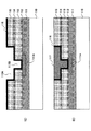
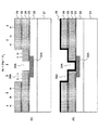
図1(A)〜図2(D)は、従来の典型的なデュアルダマシン法による配線層の形成工程を示す図である。 FIG. 1A to FIG. 2D are diagrams showing a wiring layer forming process by a conventional typical dual damascene method.
図1(A)を参照するに、シリコン基板110上に形成されたSiO2膜111上にはCuなどの低抵抗金属よりなる配線パターン111Aが埋設されており、図1(B)の工程において、前記SiO2膜111上にはSiNなどのエッチングストッパ膜112を介して低誘電率層間絶縁膜113、SiNなどのエッチングストッパ膜114および低誘電率層間絶縁膜115が形成される。
Referring to FIG. 1A, a
次に図1(C)の工程において前記層間絶縁膜113および115中に配線溝やビアホールなどの凹部113A,113Bが、前記ビアホール113Bの底部において前記Cu配線パターン111Aが露出するように、前記SiN膜114をエッチングストッパ膜として形成され、さらに図2(C)の工程において前記図1(B)の構造上に前記凹部底面および側壁面を覆うようにバリアメタル膜116が形成される。
Next, in the step of FIG. 1C, the SiN so that the
さらに図2(D)の工程において前記凹部113A,113BをCu膜で充填した後(図示せず)、前記層間絶縁膜113上の余分なCu膜および前記層間絶縁膜上面のバリアメタル膜114をCMP法で研磨・除去し、図2(D)に示すように前記凹部113A,113BがCu材料で充填されて、Cu配線パターンあるいはCuプラグなどの導電パターン117の構造が得られる。
このような従来の多層配線構造の形成方法においては、前記ビアホール113Bの形成が、前記層間絶縁膜113のドライエッチングプロセスにより行われるが、これに関連して様々な問題が生じる。
In such a conventional method for forming a multilayer wiring structure, the
図3(A),(B)は、図2(C)の工程において、前記ビアホール113Bを形成した後、バリアメタル膜116を形成するまでの工程を示す。ただし図3(A),(B)は、図2(C)の構造において前記ビアホール113Bの近傍を拡大して示している。
FIGS. 3A and 3B show steps from the formation of the
図3(A)を参照するに、前記層間絶縁膜113中にビアホール113Bをドライエッチングプロセスにより形成すると、例えば低誘電率層間絶縁膜の構成成分であるメチル基などのエッチング残渣がビアホール113の側壁面や層間絶縁膜113の表面に結合して終端される場合が生じる。また図3(A)に示すビアホール113を形成された基板を大気中に保持した場合には、前記層間絶縁膜113の表面および前記ビアホール113B、さらに図示はしないが配線溝11Aの側壁面に大気中の水分や有機物が付着するのみならず、前記ビアホール113Bの底部において前記Cu配線パターン111Aが大気中の酸素により酸化され、酸化層111Oxが形成されてしまう。このうち、前記水分や有機物の大部分は、不活性ガスを流しながら加熱する脱ガス工程を行うことにより、除去することができるが、前記酸化層111Oxはこのような脱ガス工程では除去できない。また層間絶縁膜113の表面に終端するメチル基なども、脱ガス工程で完全に除去するのは困難である。
Referring to FIG. 3A, when a
そこで図3(B)の工程において、このような構造上に前記バリアメタル膜116をスパッタ法、CVD法あるいはALD法などにより、そのまま単純に形成してしまうと、前記メチル基など、前記層間絶縁膜113の表面およびビアホール113Bの側壁面に残留する不純物を核とした核生成が生じ、図3(B)に示すように形成されるバリアメタル膜116は不連続な、あるいは層間絶縁膜115の表面を露出する欠陥の多い膜となってしまう。この場合、前記ビアホール113BをCu配線材料で充填すると、Cu原子がこれらバリアメタル膜116中の欠陥116Aの欠陥部を介して前記層間絶縁膜113中に拡散し、比誘電率の増大やリーク電流の増大など、様々な問題を引き起こす。さらに前記配線パターン111には、前記ビアホール113Bの底部に対応して前記酸化層111Oxが存在するため、前記ビアホール113BにおいてCu材料との密着不良やCu配線111Aのコンタクト抵抗が増大する問題が生じる。
Therefore, in the step of FIG. 3B, if the
これに対し従来、図3(A)の工程の後、前記バリアメタル116の堆積前に前記層間絶縁膜113の表面および前記ビアコンタクト113Bの側壁面、さらに前記ビアコンタクト113Bにより露出されたCu配線パターン111Aの表面をArプラズマでクリーニングし、前記層間絶縁膜113の表面およびビアホール113Bの側壁面から、前記メチル基などの不純物を除去すると同時に、前記ビアホール113Bの底部に露出された酸化層111Oxをスパッタエッチングにより除去する前処理技術が知られている。
In contrast, conventionally, after the step of FIG. 3A, before the deposition of the
しかし、このような従来技術では、配線パターンを形成した際に前記ビアホール113B側壁面に付着した不純物は除去できても、前記酸化層111Oxのスパッタエッチングの場合は、図4に示すようにスパッタエッチされた銅酸化物111xが前記ビアホール113Bの側壁面に再付着してしまう場合がある。この場合、付着した銅酸化物111xは前記ビアホール113Bの側壁面に直接に接しているため、その後でバリアメタル膜116を形成しても、前記銅酸化物111xから層間絶縁膜113中へのCu原子の拡散は抑制することができない。
However, in such a conventional technique, even if the impurities attached to the side wall surface of the
さらにこのような従来の前処理では、プラズマのエネルギにより低誘電率層間絶縁膜が変質し、半導体装置の高速動作にとってクリティカルなビアコンタクト部において比誘電率が増大してしまう問題が生じる。すなわち前記層間絶縁膜が組成であるメチル基などの基を含む低密度膜である場合、プラズマ処理によりビアホール側壁面に不純物として付着している基のみならず、膜を構成している基までが除去され、層間絶縁膜の密度、従って比誘電率が、前記ビアコンタクト部周辺で局所的に増大してしまう問題が生じる。 Further, in such a conventional pretreatment, the low dielectric constant interlayer insulating film is altered by the plasma energy, and there arises a problem that the relative dielectric constant increases in a via contact portion critical for high-speed operation of the semiconductor device. That is, when the interlayer insulating film is a low-density film containing a group such as a methyl group as a composition, not only a group attached as an impurity to the via hole side wall surface by plasma processing but also a group constituting the film. As a result, the density of the interlayer insulating film, and thus the relative dielectric constant, locally increases around the via contact portion.
本発明は上記の課題を解決した、新規で有用な基板処理方法および半導体装置の製造方法を提供することを概括的課題とする。 SUMMARY OF THE INVENTION It is a general object of the present invention to provide a new and useful substrate processing method and semiconductor device manufacturing method that solve the above-mentioned problems.
本発明のより具体的な課題は、ビアホールを層間絶縁膜中にドライエッチングプロセスにより形成する際に前記ビアホールの側壁面に付着した不純物を除去し活性名面を露出させ、前記ビアホール底において露出された配線パターンをスパッタすることなく、しかもビアホール底の露出部分に形成された金属酸化膜を金属膜に変換できる基板処理方法および半導体装置の製造方法を提供することにある。 A more specific problem of the present invention is that, when a via hole is formed in an interlayer insulating film by a dry etching process, impurities attached to the side wall surface of the via hole are removed to expose an active name surface, which is exposed at the bottom of the via hole. Another object of the present invention is to provide a substrate processing method and a semiconductor device manufacturing method capable of converting a metal oxide film formed on an exposed portion of the bottom of a via hole into a metal film without sputtering the wiring pattern.
本発明は、上記の課題を、
請求項1に記載したように、
層間絶縁膜中にビアホールを、前記層間絶縁膜の下に形成された低抵抗金属配線パターンが、前記ビアホールの底面において露出するように形成する工程と、
前記層間絶縁膜上に、前記ビアホールの側壁面および前記露出された低抵抗金属配線パターンを覆うように、前記ビアホールの形状に整合して導電性バリア膜を形成する工程と、
前記導電性バリア膜上に低抵抗金属膜を形成する工程と
よりなる半導体装置の製造方法であって、
前記ビアホール形成工程の後、前記導電性バリア膜の形成工程の前に、前記層間絶縁膜を、前記ビアホールの側壁面および前記ビアホールの底面を含めて、前記低抵抗金属パターンのスパッタが生じないようなエネルギの水素を含むプラズマで処理し、前記層間絶縁膜表面を、前記ビアホールの側壁面および前記ビアホールの底面を含めて水素終端する前処理工程を含むことを特徴とする半導体装置の製造方法により、または
請求項2に記載したように、
前記前処理工程において前記プラズマの電子温度は、3eVを超えないことを特徴とする請求項1記載の半導体装置の製造方法により、または
請求項3に記載したように、
前記前処理工程において前記プラズマは、マイクロ波により励起されることを特徴とする請求項1または2記載の半導体装置の製造方法により、または
請求項4に記載したように、
前記プラズマは、平面アンテナよりマイクロ波を放射することにより励起されることを特徴とする請求項1〜3のうち、いずれか一項記載の半導体装置の製造方法により、または
請求項5に記載したように、
前記プラズマは、誘導コイルに供給される高周波により励起されることを特徴とする請求項1または2記載の半導体装置の製造方法により、または
請求項6に記載したように、
前記プラズマは、リモートプラズマ源により形成されることを特徴とする請求項1記載の半導体装置の製造方法により、または
請求項7に記載したように、
前記前処理工程において前記プラズマは、希ガスと、水素を含む還元ガスの混合ガスプラズマであることを特徴とする請求項1〜6のうち、いずれか一項記載の半導体装置の製造方法により、または
請求項8に記載したように、
前記導電性バリア膜を形成する工程は、前記層間絶縁膜表面を、前記ビアホールの側壁面および底面を含めて導電性金属窒化物膜により覆う工程と、前記導電性金属窒化物膜を高融点金属膜で覆う工程とよりなることを特徴とする請求項1〜7のうち、いずれか一項記載の半導体装置の製造方法により、または
請求項9に記載したように、
前記導電性金属窒化物膜を形成する工程は、前記層間絶縁膜表面を、前記ビアホールの側壁面および底面を含めて、窒素を含む有機金属原料分子で覆う第1の工程と、前記有機金属原料分子を分解する第2の工程とよりなり、前記第1の工程と前記第2の工程とは、間にパージ工程を挟みながら繰り返されることを特徴とする請求項1〜8のうち、いずれか一項記載の半導体装置の製造方法により、または
請求項10に記載したように、
前記高融点金属膜を形成する工程は、前記導電性金属窒化物膜表面を、前記高融点金属膜を構成する高融点金属元素を含む金属原料分子で覆う第3の工程と、前記金属原料分子を分解する第4の工程とよりなり、前記第3の工程と前記第4の工程とは、間にパージ工程を挟みながら繰り返されることを特徴とする請求項9記載の半導体装置の製造方法により、または
請求項11に記載したように、
前記層間絶縁膜は、プラズマCVD法により形成されたSiOCH膜であることを特徴とする請求項1〜10のうち、いずれか一項記載の半導体装置の製造方法により、または
請求項12に記載したように、
前記層間絶縁膜は、無機SOD膜であることを特徴とする請求項1〜10のうち、いずれか一項記載の半導体装置の製造方法により、または
請求項13に記載したように、
前記層間絶縁膜は、有機ポリマー膜であることを特徴とする請求項1〜10のうち、いずれか一項記載の半導体装置の製造方法により、または
請求項14に記載したように、
前記層間絶縁膜は多孔質膜であることを特徴とする請求項1〜13のうち、いずれか一項記載の半導体装置の製造方法により、または
請求項15に記載したように、
前記導電性バリア膜を形成する工程は第1の処理容器において実行され、前記低抵抗金属膜を形成する工程は前記第1の処理容器に真空搬送室により結合された第2の処理容器において実行されることを特徴とする請求項1〜14のうち、いずれか一項記載の半導体装置の製造方法により、または
請求項16に記載したように、
前記前処理工程は第1の処理容器において実行され、前記導電性バリア膜を形成する工程は前記第1の処理容器に第1の真空搬送室を介して結合された第2の処理容器において実行され、
前記低抵抗金属膜を形成する工程は、前記第1の真空搬送室にゲートバルブを介して結合された第2の真空搬送室に結合された第3の処理容器において実行されることを特徴とする請求項1〜14のうち、いずれか一項記載の半導体装置の製造方法により、または
請求項17に記載したように、
絶縁膜中に、前記絶縁膜の下に形成された金属パターンを、底面において露出するようにビアホールを形成する工程と、
前記絶縁膜上に、前記ビアホールの側壁面および前記露出された金属パターンを覆うように、前記ビアホールの形状に整合して導電性バリア膜を形成する工程と、
よりなる基板処理方法であって、
前記ビアホール形成工程の後、前記導電性バリア膜の形成工程の前に、前記絶縁膜を、前記ビアホールの側壁面および底面を含めて、前記金属パターンのスパッタが生じないようなエネルギの水素を含むプラズマで処理し、前記絶縁膜を、前記ビアホールの側壁面および底面を含めて水素終端する工程を含むことを特徴とする基板処理方法により、解決する。
The present invention solves the above problems.
As described in
Forming a via hole in the interlayer insulating film so that a low-resistance metal wiring pattern formed under the interlayer insulating film is exposed on a bottom surface of the via hole;
Forming a conductive barrier film on the interlayer insulating film so as to match the shape of the via hole so as to cover the sidewall surface of the via hole and the exposed low-resistance metal wiring pattern;
A method of manufacturing a semiconductor device comprising a step of forming a low-resistance metal film on the conductive barrier film,
After the via hole forming step and before the conductive barrier film forming step, the interlayer insulating film including the side wall surface of the via hole and the bottom surface of the via hole is prevented from being sputtered by the low resistance metal pattern. And a pretreatment step of treating the surface of the interlayer insulating film with a plasma containing hydrogen having a sufficient energy, including a sidewall surface of the via hole and a bottom surface of the via hole, by a method for manufacturing a semiconductor device, Or as described in
The method of manufacturing a semiconductor device according to
The method according to
The said plasma is excited by radiating | emitting a microwave from a planar antenna, The manufacturing method of the semiconductor device as described in any one of Claims 1-3 characterized by the above-mentioned, or Claim 5 like,
The method according to
The method according to
In the pretreatment step, the plasma is a mixed gas plasma of a rare gas and a reducing gas containing hydrogen. According to the method for manufacturing a semiconductor device according to any one of
The step of forming the conductive barrier film includes a step of covering the surface of the interlayer insulating film with a conductive metal nitride film including a side wall surface and a bottom surface of the via hole, and covering the conductive metal nitride film with a refractory metal. The method of manufacturing a semiconductor device according to any one of
The step of forming the conductive metal nitride film includes a first step of covering the surface of the interlayer insulating film with an organometallic material molecule containing nitrogen, including a sidewall surface and a bottom surface of the via hole, and the organometallic material 9. The method according to
The step of forming the refractory metal film includes a third step of covering the surface of the conductive metal nitride film with a metal source molecule containing a refractory metal element constituting the refractory metal film, and the metal source molecule. 10. The method of manufacturing a semiconductor device according to claim 9, wherein the third step and the fourth step are repeated with a purge step interposed therebetween. Or as described in
13. The semiconductor device manufacturing method according to
The interlayer insulating film is an inorganic SOD film, or the semiconductor device manufacturing method according to any one of
The interlayer insulating film is an organic polymer film, according to the method for manufacturing a semiconductor device according to any one of
The method for manufacturing a semiconductor device according to any one of
The step of forming the conductive barrier film is performed in a first processing container, and the step of forming the low-resistance metal film is performed in a second processing container coupled to the first processing container by a vacuum transfer chamber. A method of manufacturing a semiconductor device according to any one of
The pretreatment process is performed in a first processing container, and the step of forming the conductive barrier film is performed in a second processing container coupled to the first processing container via a first vacuum transfer chamber. And
The step of forming the low-resistance metal film is performed in a third processing container coupled to a second vacuum conveyance chamber coupled to the first vacuum conveyance chamber via a gate valve. According to any one of
Forming a via hole in the insulating film so that the metal pattern formed under the insulating film is exposed on the bottom surface;
Forming a conductive barrier film on the insulating film so as to match the shape of the via hole so as to cover the sidewall surface of the via hole and the exposed metal pattern;
A substrate processing method comprising:
After the via hole formation step and before the conductive barrier film formation step, the insulating film includes hydrogen having an energy that prevents the sputtering of the metal pattern including the side wall surface and the bottom surface of the via hole. The problem is solved by a substrate processing method comprising a step of processing with plasma and terminating the insulating film with hydrogen including the side wall surface and the bottom surface of the via hole.
本発明によれば、層間絶縁膜中に金属配線パターンを露出するビアホールを形成し、さらに前記絶縁膜上に前記ビアホールの側壁面および前記露出された金属配線パターンを覆うように導電性バリア膜を形成する際、前記導電性バリア膜を形成する前に、前記層間絶縁膜表面およびビアホールの側壁面、さらに前記ビアホールの底面に露出された金属配線パターンに対して前記前処理を適用することにより、前記ビアホール形成時に前記層間絶縁膜のドライエッチングにより前記ビアホール側壁面に付着した不純物等を除去することができ、しかも前記金属配線パターンがスパッタされることがないため、ビアホール側壁面への金属汚染が生じることもない。さらに前記前処理を、水素を含むプラズマで行うため、前記ビアホール底に金属酸化物が形成されていてもこれが還元され、前記ビアホールを介したコンタクト抵抗が低減される。また、前記前処理を、水素を含むプラズマで行うため、前記層間絶縁膜の表面およびビアホール側壁面、さらに底面が水素終端され、不純物を吸着しにくい安定な構造が得られる。さらに本発明によれば、このような前処理を低エネルギプラズマにより実行することにより、前記層間絶縁膜表面に付着した不純物は除去されるが層間絶縁膜自体が変質することはなく、比誘電率の増大などの問題が生じることはない。 According to the present invention, a via hole exposing a metal wiring pattern is formed in the interlayer insulating film, and a conductive barrier film is further formed on the insulating film so as to cover the sidewall surface of the via hole and the exposed metal wiring pattern. When forming, before forming the conductive barrier film, by applying the pretreatment to the surface of the interlayer insulating film and the side wall surface of the via hole, the metal wiring pattern exposed on the bottom surface of the via hole, Impurities and the like attached to the via hole side wall surface can be removed by dry etching of the interlayer insulating film during the formation of the via hole, and the metal wiring pattern is not sputtered. It does not occur. Further, since the pretreatment is performed with plasma containing hydrogen, even if a metal oxide is formed at the bottom of the via hole, it is reduced, and the contact resistance through the via hole is reduced. Further, since the pretreatment is performed with plasma containing hydrogen, the surface of the interlayer insulating film, the side wall surface of the via hole, and the bottom surface are terminated with hydrogen, and a stable structure that hardly absorbs impurities can be obtained. Further, according to the present invention, by performing such pretreatment with low energy plasma, impurities adhering to the surface of the interlayer insulating film are removed, but the interlayer insulating film itself is not altered and the relative dielectric constant is reduced. Problems such as an increase in
本発明は特に比誘電率が3.0以下の、いわゆるlow−K膜とよばれる低密度絶縁膜を使うプロセスにおいて有効である。これらの低密度絶縁膜には、CVD法で形成されたSiOCH膜や無機SOD膜、さらに有機ポリマー膜、およびこれらの多孔質膜が含まれる。 The present invention is particularly effective in a process using a low-density insulating film called a so-called low-K film having a relative dielectric constant of 3.0 or less. These low density insulating films include SiOCH films and inorganic SOD films formed by CVD, organic polymer films, and porous films thereof.
[第1実施例]
最初に、本発明の原理を本発明の第1実施例として説明する。
[First embodiment]
First, the principle of the present invention will be described as a first embodiment of the present invention.
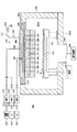
図5および図6は、本発明で使われるプラズマ処理装置10の構成を示す。
5 and 6 show the configuration of the
図5を参照するに、プラズマ処理装置10は被処理基板Wを保持する基板保持台11Bを収納し、前記基板保持台11Bとともにプロセス空間11Aを画成する処理容器11を含み、前記基板保持台11Bの外縁部には、前記処理容器11の内壁面との間にリング状の排気ポート11Cが形成される。
Referring to FIG. 5, the
前記処理容器11にはダクト16を介してポンプ17が結合され、前記プロセス空間11A中で生じた反応ガスは前記ポンプ17の作用nより前記排気ポート11cから前記ダクト16を通り、さらに排ガス処理の後、系外に排出される。前記ポンプ17としては、ドライポンプや、ドライポンプでブーストされたターボ分子ポンプを使うことができる。
A
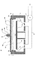
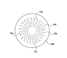
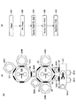
前記プロセス空間11Aの上部は、前記処理容器11上にシールリング12aを介して保持された、石英やアルミナなどの低損失セラミックよりなるプレート12により塞がれており、前記プレート12上には、ディスク状の導電性シールド部材13Aと、前記シールド部材13Aのアンテナ開口部を覆うように形成され、図6に示す多数のスロット13a,13bを含むラジアルラインスロットアンテナ13Bと、前記シールド部材13Aと前記ラジアルラインスロットアンテナ13Bとの間に形成され、SiO2やAl2O3などの膜よりなり、マイクロ波波長を圧縮する遅相板13Cとよりなる、アンテナ本体13が結合されている。図6を参照するに、前記スロット13a,13bは同心円状に、かつ互いに直交するように形成されている。
The upper portion of the
そこで前記アンテナ本体13に、前記シールド部材13Aに接続された外側導波管14Aと前記ラジアルラインスロットアンテナ13Bに結合された内側導波管14Bとよりなる同軸導波管14よりマイクロ波を供給すると、供給されたマイクロ波は前記シールド部材13Aとラジアルラインスロットアンテナ13Bとの間を径方向に伝播し、前記直交するスロット13a,13bより放射される。このようにして放射されたマイクロ波は互いに直交する偏波面を有し、全体として円偏波を形成する。
Therefore, when microwaves are supplied to the
そこでこの状態で前記プロセス空間11A中に、前記処理容器11中に形成されたガス通路15より、ArやHe、Kr,Xe,Neなどの希ガスを、必要に応じて水素などのプロセスガスとともに導入することにより、前記プロセス空間11A中に電子温度が2〜3eV以下の、非常に電子温度が低く、かつ電子密度が1012cm-3を超えるような低ダメージの高密度プラズマ16を、形成することができる。
Therefore, in this state, a rare gas such as Ar, He, Kr, Xe, Ne or the like, together with a process gas such as hydrogen, is supplied into the
本発明では、先に説明した図3(A)の構造に対して前処理を行う際に、かかる前処理を、低ダメージのプラズマを使って実行する。例えばマイクロ波プラズマ処理装置10により形成された低ダメージの高密度プラズマを使うことにより、前記層間絶縁膜表面あるいはビアホールの側壁面、さらに底面に付着していた有機基などの不純物は完全に除去され活性面が形成される一方、プラズマの電子温度が低いため、前記ビアホール底に露出していた金属配線パターンがスパッタされることはなく、このため金属がバリアメタルを形成する前の層間絶縁膜表面あるいはビアホール側壁面に付着することがない。
In the present invention, when pre-processing is performed on the structure of FIG. 3A described above, such pre-processing is performed using low-damage plasma. For example, by using a low-damage high-density plasma formed by the microwave
またかかるプラズマを形成する際に前記希ガスに水素を添加することにより、前記ビアホール底に露出されている酸化物がH2で還元され、金属酸化物を金属膜に改質することで低抵抗ビアコンタクトが得られるとともに、前記層間絶縁膜表面およびビアホール側壁面、さらに前記ビアホール底面が水素終端され、不純物の付着が生じにくい安定な構造が得られる。 Further, by adding hydrogen to the rare gas when forming such plasma, the oxide exposed at the bottom of the via hole is reduced with H 2 , and the metal oxide is reformed into a metal film to reduce the resistance. A via contact is obtained, and the surface of the interlayer insulating film, the side wall surface of the via hole, and the bottom surface of the via hole are hydrogen-terminated, thereby obtaining a stable structure in which impurities are hardly attached.
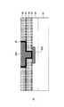
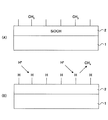
以下、本発明の第1実施例による多層配線構造の形成方法を、図7(A)〜図10(H)を参照しながら説明する。 Hereinafter, a method for forming a multilayer wiring structure according to the first embodiment of the present invention will be described with reference to FIGS. 7 (A) to 10 (H).
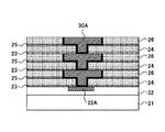
図7(A)を参照するに、シリコン基板21上に200nmの厚さに形成されたSiO2膜22中には幅が0.1μmで厚さが100nmのCuパターンがダマシン法により、前記SiO2膜22の表面において露出するように形成されており、図7(B)の工程で図7(A)の構造上に、SiNバリア兼エッチングストッパ膜23と、SiCOH層間絶縁膜24と、SiNエッチングストッパ膜25と、SiCOH層間絶縁膜26と、SiNエッチングストッパ膜27とが、順次プラズマCVD法により形成される。
Referring to FIG. 7A, in the SiO 2 film 22 formed on the
前記SiOCH膜24,26としては、市販のプラズマCVD法膜を使うことができるが、例えばかかるSiOCH膜24,26の形成を図示しない平行平板型高周波プラズマCVD装置で行う場合は、成膜を、約399Pa(3Torr)の圧力下、基板温度25℃で、Arガスを50SCCM、水素ガスを500SCCMの流量で供給し、周波数が13.50MHzの高周波を1000Wのパワーで供給することにより行うことができる。このようにして形成されたSiOCH膜24,26は約3.0の比誘電率を有する。またこのようなSiOCH膜の多孔質膜は、約2.2の比誘電率を有する。
As the
次に図8(C)の工程において図示しないフォトリソグラフィ工程により前記SiN膜27を所望の配線パターンにパターニングし、さらに前記SiN膜27をハードマスクに前記層間絶縁膜26を前記SiN膜25が露出するまでドライエッチングし、前記層間絶縁膜26中に所望の配線パターンに対応した溝部26Aを形成する。さらに図8(C)の工程では前記溝部26A中に露出した前記SiN膜25を所望のビアコンタクトにパターニングし、前記SiN膜25およびSiN膜27をハードマスクに前記層間絶縁膜24を前記SiN膜23が露出するまでドライエッチングし、前記層間絶縁膜24中に、前記ビアコンタクトに対応して開口部24Aを形成する。なお図8(C)の工程で前記溝部26Aを形成する工程と開口部24Aを形成する工程の順序は逆転させてもよい。
Next, in the step of FIG. 8C, the
次に図8(D)の工程において、前記開口部24Aの底部に露出したSiN膜23をエッチバックにより除去し、前記開口部24Aの底部に前記Cu配線パターンを露出させる。またこのSiN膜のエッチバック工程により、前記層間絶縁膜26上のSiN膜27が除去され、さらに前記配線溝26Aの底部のSiN膜25が除去される。
Next, in the step of FIG. 8D, the
このようにして得られた構造では、先に図3(A)と同様に、配線溝26Aあるいはビアホール24Aのドライエッチングで除去された膜の一部がメチル基などの形で配線溝26Aおよびビアホール24Aの側壁面および底面に吸着・結合しており、このままバリアメタル膜の堆積を行うと、バリアメタル膜の膜質が著しく劣化してしまう。またこのようにして得られた構造を大気中に保持した場合には、前記層間絶縁膜26および24の表面に水分や大気中の有機物が付着するのみならず、前記Cu配線パターン22Aのうち、前記ビアホール24Aで大気露出された部分には酸化膜22aが形成されてしまう。
In the structure thus obtained, as in FIG. 3A, a part of the film removed by dry etching of the
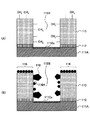
そこで本実施例ではこのようにして得られた構造上にバリアメタル膜を形成する場合、最初に脱ガス処理を行って大気中で吸着した水分や有機物を除去した後、図9(E)の工程において前記構造を図5,6のプラズマ処理装置10中に導入し、前記層間絶縁膜24および26の表面、さらに配線溝26A,ビアホール24Aの側壁面および底面に結合している有機基などの不純物を除去する前処理を行う。
Therefore, in this embodiment, when a barrier metal film is formed on the structure thus obtained, first, degassing treatment is performed to remove moisture and organic substances adsorbed in the atmosphere, and then the structure shown in FIG. In the process, the structure is introduced into the
より具体的には、13.3〜1330Pa(0.10〜10Torr)の圧力下、50〜250°C、好ましくは200℃以下の基板温度でArガスあるいはHeガスおよび水素ガスを、いずれも100〜1000SCCMの流量で供給し、さらに前記ラジアルラインスロットアンテナ13より周波数が2.45GHzのマイクロ波を1000〜5000Wのパワーで供給して前記前処理を実行する。これにより、前記層間絶縁膜26の表面、配線溝26Aの側壁面および底面、さらに前記ビアホール24Aの側壁面および底面に吸着していたメチル基などの不純物が除去される。また前記プラズマが水素を含んでいるため、前記金属酸化膜22aが還元されて前記ビアホール24Aの底部には、清浄なCuパターン22Aの金属表面が露出される。さらに前記層間絶縁膜26の表面および配線溝26Aの側壁面および底面、さらに前記ビアホール24Aの表面および側壁面は、プラズマ中に水素により終端される。
More specifically, Ar gas, He gas, and hydrogen gas are both 100 at a substrate temperature of 50 to 250 ° C., preferably 200 ° C. or less, under a pressure of 13.3 to 1330 Pa (0.10 to 10 Torr). The pre-processing is performed by supplying a microwave having a frequency of 2.45 GHz from the radial
次に図9(F)の工程において図9(E)の構造は図12に示す成膜装置300中に導入され、TaN膜とTa膜とを積層したバリアメタル膜28が、成膜ガスと還元ガスとを間にパージ工程を挟みながら繰り返し供給することで成膜を行う、いわゆるALD法により実行される。
Next, in the step of FIG. 9F, the structure of FIG. 9E is introduced into the
図12を参照するに、成膜装置300は、排気管319を介して排気装置320により排気されるプロセス空間301Aを画成する処理容器301を有し、前記プロセス空間301A中には被処理基板Wを保持するサセプタ302が納められている。前記サセプタ302にはヒータ303が埋め込まれ、前記ヒータ303を駆動電源304より駆動することにより、前記被処理基板Wが所定の温度に加熱される。また前記処理容器301の上部301aには、前記サセプタ302上の被処理基板Wに対向するように、シャワーヘッド330が絶縁部材305を介して設けられている。
Referring to FIG. 12, a
前記シャワーヘッド330の上面には、原料ガスを導入するためのガス導入口306と、H2などの還元ガスを導入するためのガス導入口307とが形成されており、前記ガス導入口306は、シャワーヘッド330の内部において形成された多数の原料ガス通路308に接続され、原料ガス通路308は、ガス分散室を介して対応する原料ガス吐出孔309に接続されている。一方前記導入口307は、シャワーヘッド330の内部において形成された多数の還元ガス通路310に接続されており、還元ガス通路310はガス分散室を介して、対応する還元ガス吐出孔311に接続されている。このような、いわゆるポストミックスタイプのシャワーヘッド330では、シャワーヘッド内部で原料ガスと還元ガスが混合されることがなく、したがってシャワーヘッド330内部において原料ガスの還元反応が生じて成膜されることがない。
A
前記ガス導入口306には、バルブ315及びマスフローコントローラ316を介して成膜原料ガス供給源312とArガスなどの不活性キャリアガス供給源313とが接続されており、前記原料ガス供給源312からの原料ガスがキャリアガス供給源313からのキャリアガスにより運搬され、前記処理容器301内のプロセス空間にシャワーヘッド330を介して供給される。また前記ガス導入口307には、バルブ315及びマスフローコントローラ316を介して還元ガス源314が接続されており、水素ガス源314からの水素ガスが前記処理容器301内に供給される。なお、図示はしていないが、プラズマCVD装置300には、前記処理容器301内にパージ用のArガスまたは窒素などの別の不活性ガスを供給するラインも設けられている。
A film forming source
さらに前記シャワーヘッド330には、整合器317及び周波数を制御するマッチャー321を介して高周波電源318が接続されており、前記高周波電源318から前記シャワーヘッド330に高周波電力を、前記マッチャー321を介して供給することにより、前記処理容器301中に供給されたガスがプラズマ励起され、これにより成膜反応が進行する。
Further, a high
図13は、図12の成膜装置300を使って実行されるALDプロセスの例を示す。
FIG. 13 shows an example of an ALD process executed using the
図13を参照するに、最初にステップ1で前記処理容器321内のプロセス空間321A中に前記成膜原料ガス源312からの原料ガスが、Arガス源313からのArキャリアガスにより導入される。このようにして導入された原料ガス中の原料分子は前記被処理基板Wの表面に化学吸着し、非常に薄い、1〜数分子層の厚さの原料分子膜が被処理基板Wの表面に形成される。
Referring to FIG. 13, first, in
次にステップ2において前記プロセス空間301A中の成膜原料ガスはArガスを導入することにより、あるいは真空引きすることによりパージされ、ステップ3において前記水素ガス源314より水素ガスが前記プロセス空間301A中に導入される。
Next, in
ステップ3では同時に前記プラズマ源318が駆動され、これにより前記プロセス空間301Aには前記水素ガスの励起により水素ラジカルや水素イオンが形成される。このようにして形成された水素ラジカルと水素イオンは前記被処理基板Wの表面に吸着していた原料分子を還元し、1〜数原子層の厚さの膜が形成される。
In
さらにステップ4において前記プロセス空間301A中の成膜原料ガスは、Arガスを再び導入することにより、あるいは真空引きすることによりパージされる。
Further, in
先にも述べたように本実施例では前記バリアメタル膜28をTaN膜とTa膜の積層により形成するが、図13のALDプロセスは、前記TaN膜の形成とTa膜の形成のいずれに対しても適用可能である。この場合、Cu層との密着性の観点から、Cu側からTaN膜およびTa膜を順次形成するのが好ましい。
As described above, in this embodiment, the
前記TaN膜をALDプロセスで形成する場合には、前記処理容器301中のプロセス空間301Aを0.133〜133Pa(0.001〜1Torr)のプロセス圧に保持し、被処理基板Wの温度を150〜350℃、好ましくは約250℃に設定し、図13のステップ1において前記成膜原料供給源312からTa(NC(CH3)2C2H5)(N(CH3)2)3をTaN膜の原料として気化器(図示せず)に10〜100mg/分の流量で供給し、気化した原料を100〜1000SCCMの流量のArキャリアガスにより前記処理容器301に供給する。ステップ1の状態を1秒間保持することにより、前記原料分子の分子層が前記被処理基板W上に形成される。
When the TaN film is formed by an ALD process, the
さらにステップ2において前記プロセス空間が、Arガスと水素ガスをそれぞれ100〜2000SCCMおよび0〜2000SCCMの流量で1秒間供給することによりパージされ、次にステップ3において前記水素ガス源314より水素ガスが200〜2000SCCMの流量で供給される。前記ステップ3ではさらに前記高周波源318が駆動され、周波数が13.56MHzの高周波が100〜2000Wのパワーで前記シャワーヘッド330に供給される。これにより、前記被処理基板Wに化学吸着していた前記Ta(NC(CH3)2C2H5)(N(CH3)2)3成膜原料分子が分解され、図9(E)の構造上に1〜数分子層の厚さのTaN膜が、前記配線溝26Aおよびビアホール24Aの側壁面および底面を連続して覆うように形成される。
Furthermore, in
さらに図13のステップ4において前記プロセス空間を、Arガスと水素ガスをそれぞれ100〜2000SCCMおよび0〜2000SCCMの流量で供給することにより1秒間パージする。パージガスは、Arガスまたは水素ガスのいずれか一方を使うことも可能である。
Further, in
さらに前記ステップ1〜4を繰り返すことにより、前記TaN膜が所望の厚さ、例えば0.1〜2nm、好ましくは0.1〜1nmの厚さに形成される。なお前記TaN膜の原料としては、上記のものの他に、Ta[N(C2H5CH3)]5(PEMAT),Ta[N(CH3)2]5(PDMAT),Ta[N(C2H5)2]5(PDEAT),Ta(NC(CH3)3)(N(C2H5)2)3(TBTDET),Ta(NC(CH3)2)3,Ta(NC2H5)2)3,Ta(N(C2H5)2)(N(C2H5)2)3等の有機金属化合物を使うことができる。
Further, by repeating the
このようにして形成されたTaN膜上にTa膜をALDプロセスで形成する場合には、前記処理容器301中のプロセス空間301Aを0.133〜133Pa(0.001〜1Torr)のプロセス圧に保持し、被処理基板Wの温度を150〜350℃に設定し、図13のステップ1において前記プロセス空間を、Arガスと水素ガスをそれぞれ100〜2000SCCMおよび0〜2000SCCMの流量で供給することにより1秒間パージする。
When a Ta film is formed on the TaN film formed in this way by an ALD process, the
次にステップ2において前記成膜原料供給源312からTaCl5をTa膜の原料として1〜10SCCMの流量で、100〜1000SCCMの流量のArキャリアガスと共に前記処理容器301に供給する。ステップ2の状態を1秒間保持することにより、前記TaCl5の分子層が前記被処理基板W上に1〜数分子層の厚さで形成される。
Next, in
さらにステップ3において前記プロセス空間が、Arガスと水素ガスをそれぞれ100〜2000SCCMおよび0〜2000SCCMの流量で5秒間供給することによりパージされ、次にステップ4において前記水素ガス源314より水素ガスが200〜2000SCCMの流量で供給される。前記ステップ4ではさらに前記高周波源318が駆動され、周波数が13.51MHzの高周波が100〜2000Wのパワーで前記シャワーヘッド330に供給される。これにより、前記被処理基板Wに化学吸着していた前記TaCl5分子が分解され、前記TaN膜上に1〜数分子のTa膜が、前記配線溝26Aおよびビアホール24Aの側壁面および底面を連続して覆うように形成される。さらに前記ステップ1〜4を繰り返すことにより、前記Ta膜が所望の厚さ、例えば0.1〜2nm、好ましくは0.5〜1nmの厚さに形成される。なお、前記Ta膜の原料としてはTaCl5以外にも、TaF5,TaBr5,TaI5等を使うことが可能である。
Further, in
このようにして図9(F)の工程でTaN/Ta積層構造のバリアメタル膜28を配線溝26Aおよびビアホール24Aの内壁面および底面に形成した後、図10(G)の工程において前記バリアメタル膜28上に、前記配線溝およびビアホールの形状に整合して、Cuシード層29を形成する。
Thus, after the
図14は、上記Cuシード層29の形成に使われるCVD装置400の構成を示す。
FIG. 14 shows a configuration of a
図14を参照するに、CVD装置400は図示しないドライポンプにより排気される処理容器411を有し、前記処理容器411中にはヒータ412Aを組み込まれた基板保持台412が設けられる。また、前記処理容器411中には、前記基板保持台412上に保持された被処理基板(図示せず)に対面するようにシャワーヘッド413が設けられ、前記シャワーヘッド413は前記基板載置台412上の基板表面にCuの気相前駆体化合物を吹き付ける。また、前記処理容器411には、ライン411Aより水素(H2)ガスが、前記Cuシード層29の堆積工程開始に先立って、前記処理容器411中の内圧を安定させるために供給される。
Referring to FIG. 14, a
前記Cu前駆体化合物は、液体の形で原料容器414に保持されており、前記原料容器414に供給されるArガスにより、バルブ415Aを備え所定の温度に保持された前駆体化合物供給ライン415に押し出される。前記ライン415に押し出された前駆体化合物は質量流量計415Bを通過し、さらに前記質量流量計415Bにより制御されるバルブ415Cを介して気化器416に供給される。前記前駆体化合物として、前記Cu+1(ヘキサフルオロアセチルアセトネート)・トリメチルビニルシラン(Cu(hfac)TMVS)を使う場合には、前記気化器416は50〜70°Cの温度に保持される。さらに、前記前駆体化合物供給ライン415には、ドレインバルブ415Dが設けられる。
The Cu precursor compound is held in a
前記気化器416において前記気相前駆体化合物はミストあるいは気体の形で噴射され、ライン16A中をバルブ16Bを介して供給される、室温あるいは60°CのH2よりなるスイープガスと共に、前記処理容器11中のシャワーヘッド413に、バルブ416Cを介して供給される。その際、前記バルブ416Cを含む気化器416から処理容器411に至る気相原料供給ライン416Dの温度は、前記Cu(hfac)TMVSをCuの前駆体化合物に使う場合には、前記前駆体化合物の再液化を防ぐため、気化器と同温程度に制御される。また前記シャワーヘッド413は50〜70°Cの温度に保持され、また処理容器411自体もシャワーヘッドと同程度の温度に保持される。
In the
前記前駆体化合物供給ライン415にはドレインが形成され、さらに前記気化器416は、バルブ416Eを介して、ドライポンプ(図示せず)により排気され、前記Cu前駆体化合物から離脱したTMVSアダクトが除去される。
A drain is formed in the precursor
図14の化学気相堆積装置を使うことにより、前記処理容器411中において、例えば化学式
2Cu+1(hfac)TMVS→2Cu+1(hfac)+2TMVS
→Cu+Cu+2(hfac)+2TMVS
に従って、Cuシード層29の堆積が生じる。なお、Cuシード層29はPVD法により形成することもできる。
By using the chemical vapor deposition apparatus of FIG. 14, in the
→ Cu + Cu +2 (hfac) + 2TMVS
Accordingly, deposition of the
図10(G)の工程の後、前記基板は図10(H)の工程において電解めっき処理装置に移され、電解めっき法あるいは無電解めっき法により前記Cuシード層29上にCu層30が形成される。
After the step of FIG. 10G, the substrate is transferred to an electrolytic plating apparatus in the step of FIG. 10H, and a
さらに熱処理の後、図11(I)の工程において前記層間絶縁膜26上のCu層30およびその下のバリアメタル膜28がCMP(化学機械研磨)法により研磨除去され、前記配線溝26Aおよびビアホール24AをCuにより充填した配線構造が得られる。
Further, after the heat treatment, in the step of FIG. 11I, the
さらに上記図7(A)〜図11(I)の工程を繰り返すことにより、図15に示すような、図11(I)の構造が繰り返された多層配線構造を形成することができる。 Further, by repeating the steps of FIGS. 7A to 11I, a multilayer wiring structure in which the structure of FIG. 11I is repeated as shown in FIG. 15 can be formed.
本実施例では図9(E)の工程において、バリアメタル膜28を堆積する前に前記層間絶縁膜26の表面、前記配線溝26Aの側壁面および底面、さらに前記ビアホール24Aの側壁面および底面を前処理するに際し、電子温度の低い高密度プラズマを使うため、層間絶縁膜24,26がダメージを受けることがなく、膜中の基がスパッタされることによる膜密度および比誘電率の局所的な増大が生じることがない。またビアホール24A底部で露出されているCu配線パターン22AがスパッタされてCuあるいはCu酸化物がビアホール24Aや配線溝26Aの側壁面に付着することがなく、このためCu原子の層間絶縁膜24あるいは26への拡散が生じることがない。
In this embodiment, in the step of FIG. 9E, before depositing the
なお、以上の説明では、前記層間絶縁膜24および26を市販の原料を使ったプラズマCVD法により形成されるSiOCH膜としたが、本発明はかかる特定の層間絶縁膜組成に限定されるものではない。一般に前記層間絶縁膜24および26としては、大別して無機系の膜と有機系の膜があり、例えば無機SOD膜(スピンコート法によって成膜される絶縁膜)であるアルキルシロキサンポリマー、HSQ(水素化シルセスキオキサンポリマー)、などを使うことができる。また、CVD(化学気相堆積)法によっても低誘電率膜は形成可能であり、このような無機膜として、例えばフッ素添加シリコン酸化膜などを使うこともできる。
In the above description, the
また、このような無機膜やシリコン酸化膜は、いずれも多孔質膜にすることによってさらに誘電率を低下させることができ、本発明はこのような多孔質膜を使う場合にも有効である。 In addition, such an inorganic film or silicon oxide film can be further reduced in dielectric constant by making it a porous film, and the present invention is also effective when such a porous film is used.
また、前記層間絶縁膜24,26として有機膜を使う場合には、PTFE系膜、ポリイミド系膜、フッ素添加ポリイミド膜、BCB(ベンゾシクロブテン)膜、パレリン−N膜、パレリン−F膜、MSQ(アルキルシルセスキオキサンポリマー)膜、HOSP(水素化アルキルシルセスキオキサンポリマー)膜などの有機ポリマー膜を使うことができる。さらに有機系の膜には、CVD法によって形成されるフッ素添加カーボン膜やDLC(ダイヤモンドライクカーボン)、SiCO膜やSiCO(H)膜などが含まれる。このような有機膜を使う場合でも、多孔質膜にすることによってさらに誘電率を低減することができ、本発明はこのような場合にも有効である。
When an organic film is used as the
また図10(G)の工程において、前記Cuシード層29をスパッタなどのPVD法により行うこともできる。
Further, in the step of FIG. 10G, the
さらに図9(F)のバリアメタル膜28の形成においては、前記Ta膜の形成をスパッタなどのPVD法により行うこともできる。またTaN膜をALD−CVD法により、またTa膜をPVD法で形成することも効果的である。
Further, in the formation of the
図9(E)のプラズマ処理工程と図9(F)のバリアメタル膜28の形成工程は、同一の処理容器内において行うことも可能ではあるが、図9(E)の工程と図9(F)の工程とでは処理温度が異なるので、これらの工程は別々の処理容器で行うのが好ましい。さらに図9(F)のバリアメタル膜成膜工程は図9(E)の前処理工程の直後に、大気に曝すことなく行う必要があるため、これら別々の処理容器は真空搬送室で結合するのが好ましい。
Although the plasma processing step in FIG. 9E and the formation step of the
さらに前記図10(G)のCuシード層29の成膜は、図9(E)の前処理工程あるいは図9(F)のALD工程よりは低圧力環境で行われるため、図10(G)の工程は前記真空搬送室に、真空度の高い別の真空搬送室を介して結合された別の処理容器において実行するのが、処理効率の観点から好ましい。前記Cuシード層29の成膜をPVD法で行う場合、および前記Ta膜の成膜をPVD法で行う場合も同様である。
[第2実施例]
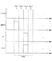
図16(A)は、このような本発明のプロセスを効率よく実行するのに適した、クラスタ型基板処理システム500の構成を、図16(B)は、前記基板システム500において実行される基板処理の流れを示す。
Further, since the
[Second Embodiment]
FIG. 16A shows a configuration of a cluster type
図16(A)を参照するに、基板処理システム500は大気環境中にカセットモジュール501A,501B、およびウェハのノッチあるいはオリエンテーションフラットを検出してウェハ方位を合わせるウェハオリエンタ501Cを有する導入側ウェハ搬送室501を有し、前記導入側ウェハ搬送室501にはゲートバルブG1,G2を介してロードロック室502A,502Bが結合されている。前記導入側ウェハ搬送室501は大気圧状態にあり、ウェハを清浄な状態で保持する。
Referring to FIG. 16A, a
前記ロードロック室502A,502BにはそれぞれのゲートバルブG3,G4を介してウェハ搬送ロボットを含む真空ウェハ搬送室503が結合されており、前記真空ウェハ搬送室503にはゲートバルブG5,G6,G7をそれぞれ介して、脱ガス処理室504Aと図5,6のマイクロ波プラズマ処理装置10を有する前処理室504Bと図12の堆積装置300を有するバリアメタル成膜処理室504Cとが結合されている。
A vacuum
さらに前記真空ウェハ搬送室503にはウェハ受け渡し室504DおよびゲートバルブG8を介してウェハ搬送ロボットを含む第2の真空ウェハ搬送室505が結合されており、前記真空ウェハ搬送室505にはゲートバルブG9を介して、図10(G)のCuシード層29の形成工程を実行するCVD室506Aが結合されている。ここで前記真空ウェハ搬送室503は、前記処理室504A〜504Cでの処理に対応して、比較的高い、10-6Torr程度の圧力に保持されているのに対し、前記真空ウェハ搬送室505は、前記処理室506Aでの処理に対応して、より低い、10-7Torr以下の圧力に保持されている。また真空搬送室503と505の圧力を同圧に、あるいは真空搬送室505の圧力を真空搬送室503の圧力よりも低く設定して、真空搬送室505の雰囲気が真空搬送室503に侵入して汚染を生じるのを抑制する。
Further, a second vacuum
図16(B)のフローチャートを参照するに、前記カセットモジュール501Aあるいは501B中には図8(D)の状態のウェハが保持されており、前記ウェハは、前記ウェハオリエンタ501Cで方位を合わされた後、前記導入側ウェハ搬送室501より前記ゲートバルブG1およびロードロック室502AあるいはゲートバルブG2およびロードロック室502Bを通って前記真空ウェハ搬送室503に導入され、さらに前記真空ウェハ搬送室503からゲートバルブG5を通って脱ガス処理室504に搬送される。前記脱ガス処理室504では不活性ガスを導入して加熱あるいは紫外光照射処理が行われるようにしてもよい。
Referring to the flowchart of FIG. 16B, the wafer in the state of FIG. 8D is held in the
前記脱ガス処理室504で大気中の水や膜中の残留ガス等を脱ガス処理の後、前記ウェハは前記ゲートバルブG5を通って真空ウェハ搬送室503に戻され、さらにステップ2において前記ゲートバルブG6を通って前記前処理室504Bに搬送され、図9(E)の工程に対応した前処理が行われる。
After the degassing treatment of the water in the atmosphere and the residual gas in the film in the degassing treatment chamber 504, the wafer is returned to the vacuum
次に前記前処理室504Bにおける脱ガス処理の後、前記ウェハは前記ゲートバルブG6を通って真空ウェハ搬送室503に戻され、さらにステップ3において前記ゲートバルブG7を通って前記成膜処理室504Cに搬送され、図9(F)の工程に対応してバリアメタル膜28の形成が、先に説明したALD工程により、なされる。
Next, after degassing in the
さらに前記成膜処理室504Cにおけるバリアメタル膜28の成膜処理の後、前記ウェハは前記成膜処理室504CからゲートバルブG7を通って真空ウェハ搬送室503に戻され、さらにウェハ受け渡し室504DからゲートバルブG8を通って真空ウェハ搬送室505に搬送される。
Further, after the deposition process of the
前記真空ウェハ搬送室505に導入されたウェハは、ステップ4において前記ゲートバルブG9を通ってCVD室506Aに導入され、図10(G)の工程に対応してCuシード層29が形成される。
The wafer introduced into the vacuum
このようにしてCuシード層29が形成された後、前記ウェハは前記ゲートバルブG9を通って真空ウェハ搬送室505に戻され、さらに前記ゲートバルブG8およびウェハ受け渡し室504Dを通って真空ウェハ搬送室503に戻される。さらに前記ウェハは前記真空搬送室503からゲートバルブG3、ロードロック室502AおよびゲートバルブG1を通って、あるいはゲートバルブG4、ロードロック室502BおよびゲートバルブG2を通って前記導入側ウェハ搬送室501に戻され、さらにカセットモジュール501Aあるいは501Bに戻される。
After the
かかる構成では、連続して処理する必要があるが処理温度が異なる脱ガス工程、図9(E)の前処理工程、および図9(F)のバリアメタル成膜工程が、真空ウェハ搬送室503で結合された別々の処理室で実行されるため、基板温度の昇降に伴う時間が短縮され、効率のよい基板処理が可能となる。また処理圧が大きく異なる図10(G)のCuシード層の形成工程が、より低圧に保持される真空ウェハ搬送室505に結合された処理室506Aにおいて実行されるため、ウェハを様々な処理容器に出し入れする際の圧力調整幅が、単一の真空ウェハ搬送室を使う場合よりも減少し、効率的な基板処理が可能になる。
In such a configuration, a degassing process that requires continuous processing but different processing temperatures, a pretreatment process in FIG. 9E, and a barrier metal film forming process in FIG. Therefore, the time required for raising and lowering the substrate temperature is shortened, and efficient substrate processing becomes possible. Further, since the process of forming the Cu seed layer of FIG. 10 (G) having a significantly different processing pressure is performed in the
なお、図16の基板処理システム500は、先に説明したような多層配線構造の形成のみならず、層間絶縁膜上にTa/TaN構造のバリアメタル膜を介してRuやIrなどの金属電極膜を形成し、その上に強誘電体膜を形成する強誘電体メモリの製造においても有用である。
[第3実施例]
図17(A)は、本発明の第3実施例による基板処理システム600の構成を示す。ただし図17(A)中、先に説明した部分には同一の参照符号を付し、説明を省略する。
Note that the
[Third embodiment]
FIG. 17A shows the configuration of a
図17(A)を参照するに、本実施例では前記CVD室506Aが除去され、その代わりに図10(G)のCuシード層29の形成工程をスパッタ法により実行するPVD室506が前記真空ウェハ搬送室505にゲートバルブG10を介して結合されている。
Referring to FIG. 17A, in this embodiment, the
図17(B)は、図17(A)の基板処理システム600を使って行われる基板処理の流れを示す。
FIG. 17B shows a flow of substrate processing performed using the
図17(B)を参照するに、図16(B)のステップ1に対応するステップ11の脱ガス処理およびステップ2に対応するステップ12の前処理の後、ステップ13において前記バリア膜28がTa膜のALDプロセスにより、あるいはTaN膜のALDプロセスにより、あるいはTaN膜とTa膜を積層するALDプロセスにより形成れる。前記バリア膜28をTa膜のみにより形成する場合は、先に説明したTa膜の形成シーケンスを所望の膜厚が得られるまで繰り返せばよく、また前記バリア膜28をTaN膜のみにより形成する場合には、先に説明したTaN膜の形成シーケンスを、所望の膜厚が得られるまで繰り返せばよい。
Referring to FIG. 17B, after the degassing process in
ステップ13の後、本実施例では前記処理室504Cから前記ウェハが前記ゲートバルブG7を通って真空ウェハ搬送室503に戻され、ステップ14において前記ウェハはウェハ受け渡し室504DおよびゲートバルブG8を介してより真空度の高い真空ウェハ搬送室505に搬送される。さらに前記ウェハはゲートバルブG10を介してPVD室506Bに搬送され、前記Cuシード層29がスパッタ法により形成される。
After
一般にスパッタ法は10-8Torr以下の圧力を必要とするため、かかるスパッタ室を圧力が10-6Torr程度の真空ウェハ搬送室503に結合すると、処理開始までに長い排気時間を必要とする。これに対し本実施例では、前記スパッタ室506Bを真空度の高い基板搬送室505に結合しているため、このような問題が生じない。
In general, since the sputtering method requires a pressure of 10 −8 Torr or less, when such a sputtering chamber is coupled to a vacuum
本発明のその他の特徴は先の実施例の通りであり、説明を省略する。
[第4実施例]
図18(A)は、本発明の第4実施例による基板処理システム700の構成を示す。ただし図18(A)中、先に説明した部分には同一の参照符号を付し、説明を省略する。
Other features of the present invention are the same as in the previous embodiment, and a description thereof will be omitted.
[Fourth embodiment]
FIG. 18A shows a configuration of a
図18(A)を参照するに、本実施例では図17(A)の実施例と同様に図16(A)のCVD室506Aが除去され、その代わりに図10(G)のCuシード層29の形成工程をスパッタ法により実行するPVD室506Bが前記真空ウェハ搬送室505にゲートバルブG10を介して結合されている。さらに本実施例では前記ウェハ真空搬送室505にゲートバルブG11を介して図9(F)のバリアメタル膜28の成膜工程のうち、Ta膜の成膜工程をスパッタ法により実行するPVD室506Cが結合されている。本実施例でも前記真空ウェハ搬送室503と真空ウェハ搬送室505は同圧に、あるいは真空ウェハ搬送室505の圧力を真空ウェハ搬送室503よりも低く設定して、真空ウェハ搬送室503中の雰囲気が真空ウェハ搬送室503に侵入して汚染を生じるのを抑制する。
Referring to FIG. 18A, in this embodiment, the
図18(B)は、図18(A)の基板処理システム700を使って行われる基板処理の流れを示す。
FIG. 18B shows a flow of substrate processing performed using the
図18(B)を参照するに、図16(B)のステップ1に対応するステップ21の脱ガス処理およびステップ2に対応するステップ22の前処理の後、ステップ23において前記バリア膜28が最初TaN膜のALD工程により、ついでステップ24においてTa膜のPVD工程により、TaN膜とTa膜の積層として形成される。
Referring to FIG. 18B, after the degassing process in
より詳細に説明すると、前記ステップ23において図9(E)の状態のウェハが前記堆積装置504Cに導入され、先に第1実施例において説明したALD工程を行うことにより、前記バリアメタル膜28のうちのTaN膜が形成される。
More specifically, in
ステップ23の後、本実施例では前記ウェハが前記処理室504Cから前記ゲートバルブG7を通って真空ウェハ搬送室503に戻され、さらにステップ24において前記ウェハはウェハ受け渡し室504DおよびゲートバルブG8を介してより真空度の高い真空ウェハ搬送室505に搬送される。さらに前記ウェハはゲートバルブG11を介してPVD室506Cに搬送され、前記Ta膜が、先に形成されたTaN膜上にスパッタ法により形成される。これにより、図9(F)のバリアメタル膜28の成膜が完了する。
After
次にステップ25において前記バリアメタル膜28が形成された図9(F)の状態のウェハは前記ゲートバルブG11を通って真空搬送室505に戻され、さらにゲートバルブG10を通って前記PVD室506Bに搬送され、前記バリアメタル膜28上に図10(G)の構造に対応してCuシード層29が形成される。
Next, in
本実施例においても高真空を要求するPVD室506Bおよび506Cが、真空度の低い真空基板搬送室505とはゲートバルブG8で隔てられた真空度の高い真空基板搬送室505に結合されているため、PVD室506Bおよび506Cにウェハを出し入れする際の圧力調整期間が短くてすみ、効率のよい基板処理が可能となる。
Also in this embodiment, the
なお本実施例ではPVD処理としてイオン化PVD処理が好ましく、ALD処理としてはプラズマALD処理を行うのが好ましい。
[第5実施例]
以上の説明では、図9(E)の低エネルギプラズマを使った前処理を、図5,6で説明したマイクロ波プラズマ処理装置10において行っているが、本発明はかかる特定のプラズマ処理装置に限定されるものではない。
In this embodiment, ionized PVD processing is preferable as PVD processing, and plasma ALD processing is preferably performed as ALD processing.
[Fifth embodiment]
In the above description, the pretreatment using the low energy plasma of FIG. 9E is performed in the microwave
図19は、図9(E)の工程において低エネルギプラズマ源として使うことのできるICP(誘導結合プラズマ)型のプラズマ処理装置800の構成を示す。
FIG. 19 shows a configuration of an ICP (inductively coupled plasma) type
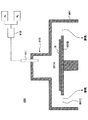
図19を参照するに、プラズマ処理装置800はプロセス空間701Aを画成する処理容器801を有し、前記プロセス空間801中には被処理基板Wを保持する基板保持台801Bが設けられている。
Referring to FIG. 19, the
前記処理容器801の上部には多数のガス吐出口802Aを有するガス導入部802が設けられており、前記ガス導入部上には石英ガラスよりなるベルジャー803が設けられている。また前記ベルジャー803にはArガスなどの希ガスと水素ガスなどのプロセスガスを供給するガス導入口803Aが形成されており、さらに前記ベルジャー803の周囲には高周波誘導コイル804が巻回されている。
A
そこで例えば1.33〜1330Pa(0.01〜10Torr)の圧力下、50〜250℃の基板温度で前記ベルジャー803中に前記ガス導入口803AよりArガスを100〜1000SCCMの流量で、あるいは前記Arガスの代わりにHeガスを100〜1000SCCMの流量で、水素ガスを100〜1000SCCMの流量で供給し、前記コイル804に周波数が450kHzの高周波を500〜5000Wのパワーで供給することにより、前記層間絶縁膜26の表面や配線溝26Aの側壁面および底面、さらに前記ビアホール24Aの側壁面や底面に付着した有機基などの不純物が除去され、さらにビアホール24A底部において露出したCuパターン22A表面の酸化層が還元される。またこのようにして形成されたプラズマは3eV以下の低い電子温度を有しており、前記層間絶縁膜24,26表面のダメージや、これに伴う比誘電率の増大の問題を生じることがなく、またCuパターン22Aをスパッタすることがない。流量比がAr<H2のプラズマで処理されるので、224表面はスパッタされない。
[第6実施例]
さらに図9(E)の前処理工程を、図20に示すリモートプラズマ源910を使った基板処理装置900にて行うことも可能である。
Therefore, for example, Ar gas is supplied into the
[Sixth embodiment]
Further, the pretreatment step of FIG. 9E can be performed by the
図20を参照するに、基板処理装置900はプロセス空間901Aを画成し被処理基板Wを保持する基板保持台901Bを含む処理容器901を有し、前記処理容器901と基板保持台901Bとの間には排気ポート901Cが形成されている。
Referring to FIG. 20, a
さらに図20の構成では前記処理容器901の一部には、前記リモートプラズマ源910が設けられ、ガスライン911より供給されたArガスあるいはHeガスを含み、さらに水素ガスを含む処理ガスを高周波によりプラズマ励起する。
Further, in the configuration of FIG. 20, the
そこで本実施例では前記基板処理装置900中に図8(D)の状態の基板21を被処理基板Wとして導入し、さらに前記リモートプラズマ源により励起されたプラズマを作用させることにより、先の実施例と同様に、前記層間絶縁膜26の表面および配線溝26Aの側壁面および底面、さらに前記ビアホール24Aの側壁面および底面に付着した有機基などの不純物を除去することができる。その際、前記プラズマの電子温度を3eV以下に抑制することにより、前記層間絶縁膜24あるいは26のダメージが回避され、比誘電率の増大が生じることはない。また前記ビアホール24Aの底面に露出したCu配線パターン22Aがスパッタされることもない。
Therefore, in this embodiment, the
このようなリモートプラズマは、例えば13.3〜133Paの圧力下、Arガスを100〜500SCCMの流量で、またはHeガスを100〜500SCCMの流量で、さらに水素ガスを1000SCCMの流量で導入し、周波数が13.56kHzの高周波を500〜2000Wのパワーで供給することにより形成することができる。 For example, such remote plasma is introduced under a pressure of 13.3 to 133 Pa, Ar gas is introduced at a flow rate of 100 to 500 SCCM, He gas is introduced at a flow rate of 100 to 500 SCCM, and hydrogen gas is introduced at a flow rate of 1000 SCCM. Can be formed by supplying a high frequency of 13.56 kHz with a power of 500 to 2000 W.
前記プラズマは水素を含むため、前記前処理の後、前記層間絶縁膜26の表面、前記配線溝26Aの側壁面および底面、さらに前記ビアホール24Aの側壁面および底面は水素終端され、不純物の付着が抑制される。
Since the plasma contains hydrogen, the surface of the
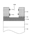
以上本発明を、低誘電率層間絶縁膜を有する多層配線構造の形成を例に説明したが、本発明は図21(A)に示すように、下地膜1上に形成されたSiOCHなどの低誘電率絶縁膜2の表面に吸着した有機基などの不純物を、図21(B)に示すように膜2にダメージを生じることなく、また比誘電率を増大させることなくクリーニングし、かつ表面を水素終端することが可能になる。
The present invention has been described above by taking the formation of a multilayer wiring structure having a low dielectric constant interlayer insulating film as an example. However, the present invention is not limited to SiOCH or the like formed on the
また先の実施例ではバリアメタル膜はTaN膜あるいはTa膜、あるいはTaN膜とTA膜を積層した構成の膜であるとして説明を行ったが、本発明はTi膜やTiN膜など、他のバリアメタル膜を使う場合でも有効である。 In the previous embodiment, the barrier metal film is described as being a TaN film, a Ta film, or a film having a structure in which a TaN film and a TA film are laminated. However, the present invention is not limited to other barriers such as a Ti film or a TiN film. This is effective even when a metal film is used.
特許請求の範囲に記載した本発明の要旨内において、様々な変形や変更が可能である。 Various modifications and changes can be made within the scope of the present invention described in the claims.
1 下地膜
2 低誘電率膜
10,800,900 プラズマ処理装置
11 処理容器
11A プロセス空間
11B 基板保持台
11C 排気ポート
12 窓
12a シールリング(Oリング)
13 アンテナ本体
13A 導波部(シールド部材)
13B ラジアルラインスロットアンテナ
13a,13bスロット
13C 遅相板
14 同軸導波管
14A 外側導波管
14B 内側導体
15 ガス導入口
21,110 シリコン基板
22,111 絶縁膜
22A,111A Cu配線パターン
22a,111Ox 酸化物
111x 銅残渣
23,25,27,112,114 エッチングストッパ膜
26,27,113,115 層間絶縁膜
26A,113A 配線溝
24A,113B ビアホール
28.116 バリアメタル膜
29 Cuシード層
30 Cu層
30A,117 Cu配線パターン
300 プラズマALD装置
301 処理容器
301a 処理容器上部
301b 処理容器底部
302 基板保持台
303 ヒータ
304 ヒータ電源
305 絶縁体
306,307,308,310 ガス通路
309,311 原料ガス吐出口
312 成膜原料源
313 Ar源
314 水素源
315 バルブ
316 MFC
317 整合器
318 高周波電源
319 排気口
320 排気装置
321 マッチャー
330 シャワーヘッド
400 CVD装置
411 処理容器
411A,416A 水素ガスライン
412 基板保持台
412A ヒータ
413 シャワーヘッド
414 Cu原料容器
415,416D 配管
415A,415C,416B,416C,416E バルブ
415B MFC
415D ドレイン
416 気化器
500,600,700 クラスタ型基板処理システム
501 導入側ウェハ搬送室(大気搬送室)
501A,501B カセットモジュール
501C ウェハオリエンタ
502A,502B ロードロック室
503,505 真空ウェハ搬送室
504A 脱ガス室
504B 前処理室
504C ALD室
504D ウェハ受け渡し室
506A CVD室
506B、506C PVD室
G1〜G9 ゲートバルブ
DESCRIPTION OF
13
13B Radial
317
501A, 501B Cassette module
Claims (17)
前記層間絶縁膜上に、前記ビアホールの側壁面および前記露出された低抵抗金属配線パターンを覆うように、前記ビアホールの形状に整合して導電性バリア膜を形成する工程と、
前記導電性バリア膜上に低抵抗金属膜を形成する工程と
よりなる半導体装置の製造方法であって、
前記ビアホール形成工程の後、前記導電性バリア膜の形成工程の前に、前記層間絶縁膜を、前記ビアホールの側壁面および前記ビアホールの底面を含めて、前記低抵抗金属パターンのスパッタが生じないようなエネルギの水素を含むプラズマで処理し、前記層間絶縁膜表面を、前記ビアホールの側壁面および前記ビアホールの底面を含めて水素終端する前処理工程を含むことを特徴とする半導体装置の製造方法。 Forming a via hole in the interlayer insulating film so that a low-resistance metal wiring pattern formed under the interlayer insulating film is exposed on a bottom surface of the via hole;
Forming a conductive barrier film on the interlayer insulating film so as to match the shape of the via hole so as to cover the sidewall surface of the via hole and the exposed low-resistance metal wiring pattern;
A method of manufacturing a semiconductor device comprising a step of forming a low-resistance metal film on the conductive barrier film,
After the via hole forming step and before the conductive barrier film forming step, the interlayer insulating film including the side wall surface of the via hole and the bottom surface of the via hole is prevented from being sputtered by the low resistance metal pattern. A method of manufacturing a semiconductor device, comprising: a pretreatment step of processing with plasma containing hydrogen of sufficient energy and hydrogen-termination of the surface of the interlayer insulating film including the side wall surface of the via hole and the bottom surface of the via hole.
前記低抵抗金属膜を形成する工程は、前記第1の真空搬送室にゲートバルブを介して結合された第2の真空搬送室に結合された第3の処理容器において実行されることを特徴とする請求項1〜14のうち、いずれか一項記載の半導体装置の製造方法。 The pretreatment process is performed in a first processing container, and the step of forming the conductive barrier film is performed in a second processing container coupled to the first processing container via a first vacuum transfer chamber. And
The step of forming the low-resistance metal film is performed in a third processing container coupled to a second vacuum conveyance chamber coupled to the first vacuum conveyance chamber via a gate valve. The manufacturing method of the semiconductor device as described in any one of Claims 1-14.
前記絶縁膜上に、前記ビアホールの側壁面および前記露出された金属パターンを覆うように、前記ビアホールの形状に整合して導電性バリア膜を形成する工程と、
よりなる基板処理方法であって、
前記ビアホール形成工程の後、前記導電性バリア膜の形成工程の前に、前記絶縁膜を、前記ビアホールの側壁面および底面を含めて、前記金属パターンのスパッタが生じないようなエネルギの水素を含むプラズマで処理し、前記絶縁膜を、前記ビアホールの側壁面および底面を含めて水素終端する工程を含むことを特徴とする基板処理方法。 Forming a via hole in the insulating film so that the metal pattern formed under the insulating film is exposed on the bottom surface;
Forming a conductive barrier film on the insulating film so as to match the shape of the via hole so as to cover the sidewall surface of the via hole and the exposed metal pattern;
A substrate processing method comprising:
After the via hole formation step and before the conductive barrier film formation step, the insulating film includes hydrogen having an energy that prevents the sputtering of the metal pattern including the side wall surface and the bottom surface of the via hole. A substrate processing method characterized by including a step of performing a hydrogen treatment on the insulating film including a side wall surface and a bottom surface of the via hole by processing with plasma.
Priority Applications (3)
| Application Number | Priority Date | Filing Date | Title |
|---|---|---|---|
| JP2004164521A JP4503356B2 (en) | 2004-06-02 | 2004-06-02 | Substrate processing method and semiconductor device manufacturing method |
| US11/142,457 US7332426B2 (en) | 2004-06-02 | 2005-06-02 | Substrate processing method and fabrication process of a semiconductor device |
| US11/673,628 US7772111B2 (en) | 2004-06-02 | 2007-02-12 | Substrate processing method and fabrication process of a semiconductor device |
Applications Claiming Priority (1)
| Application Number | Priority Date | Filing Date | Title |
|---|---|---|---|
| JP2004164521A JP4503356B2 (en) | 2004-06-02 | 2004-06-02 | Substrate processing method and semiconductor device manufacturing method |
Publications (2)
| Publication Number | Publication Date |
|---|---|
| JP2005347472A true JP2005347472A (en) | 2005-12-15 |
| JP4503356B2 JP4503356B2 (en) | 2010-07-14 |
Family
ID=35449543
Family Applications (1)
| Application Number | Title | Priority Date | Filing Date |
|---|---|---|---|
| JP2004164521A Expired - Fee Related JP4503356B2 (en) | 2004-06-02 | 2004-06-02 | Substrate processing method and semiconductor device manufacturing method |
Country Status (2)
| Country | Link |
|---|---|
| US (2) | US7332426B2 (en) |
| JP (1) | JP4503356B2 (en) |
Cited By (10)
| Publication number | Priority date | Publication date | Assignee | Title |
|---|---|---|---|---|
| WO2007086126A1 (en) * | 2006-01-26 | 2007-08-02 | Fujitsu Limited | Ferroelectric memory device, method for manufacturing such ferroelectric memory device and method for manufacturing semiconductor device |
| WO2008146879A1 (en) * | 2007-05-30 | 2008-12-04 | Tokyo Electron Limited | Semiconductor device manufacturing method, semiconductor manufacturing apparatus and storage medium |
| WO2010059434A3 (en) * | 2008-11-19 | 2010-07-29 | Micron Technology, Inc. | Methods for forming a conductive material, methods for selectively forming a conductive material, methods for forming platinum, and methods for forming conductive structures |
| JP2010533987A (en) * | 2007-07-20 | 2010-10-28 | アイメック | Damascene contact in III-V CMOS devices |
| US8598706B2 (en) | 2007-09-18 | 2013-12-03 | Renesas Electronics Corporation | Method for forming interlayer dielectric film, interlayer dielectric film, semiconductor device and semiconductor manufacturing apparatus |
| JP2014099627A (en) * | 2006-08-30 | 2014-05-29 | Lam Research Corporation | Processes and integrated systems for conditioning substrate surface for metal deposition |
| US8999841B2 (en) | 2011-08-05 | 2015-04-07 | Tokyo Electron Limited | Semiconductor device manufacturing method |
| JP2015092548A (en) * | 2013-09-16 | 2015-05-14 | エスピーティーエス テクノロジーズ リミティド | Pre-cleaning of semiconductor structure |
| US9576850B2 (en) | 2012-01-25 | 2017-02-21 | Tokyo Electron Limited | Method for manufacturing semiconductor device |
| US12538780B2 (en) | 2022-09-22 | 2026-01-27 | Kabushiki Kaisha Toshiba | Isolator |
Families Citing this family (325)
| Publication number | Priority date | Publication date | Assignee | Title |
|---|---|---|---|---|
| US20060226003A1 (en) * | 2003-01-22 | 2006-10-12 | John Mize | Apparatus and methods for ionized deposition of a film or thin layer |
| US20050178328A1 (en) * | 2004-02-17 | 2005-08-18 | Matsushita Electric Industrial Co., Ltd. | Film forming method and film forming apparatus |
| US7253125B1 (en) | 2004-04-16 | 2007-08-07 | Novellus Systems, Inc. | Method to improve mechanical strength of low-k dielectric film using modulated UV exposure |
| JP4503356B2 (en) * | 2004-06-02 | 2010-07-14 | 東京エレクトロン株式会社 | Substrate processing method and semiconductor device manufacturing method |
| US7605469B2 (en) | 2004-06-30 | 2009-10-20 | Intel Corporation | Atomic layer deposited tantalum containing adhesion layer |
| US9659769B1 (en) | 2004-10-22 | 2017-05-23 | Novellus Systems, Inc. | Tensile dielectric films using UV curing |
| US7790633B1 (en) | 2004-10-26 | 2010-09-07 | Novellus Systems, Inc. | Sequential deposition/anneal film densification method |
| US7510982B1 (en) | 2005-01-31 | 2009-03-31 | Novellus Systems, Inc. | Creation of porosity in low-k films by photo-disassociation of imbedded nanoparticles |
| US9659758B2 (en) * | 2005-03-22 | 2017-05-23 | Honeywell International Inc. | Coils utilized in vapor deposition applications and methods of production |
| US8282768B1 (en) | 2005-04-26 | 2012-10-09 | Novellus Systems, Inc. | Purging of porogen from UV cure chamber |
| US8889233B1 (en) | 2005-04-26 | 2014-11-18 | Novellus Systems, Inc. | Method for reducing stress in porous dielectric films |
| US8980769B1 (en) | 2005-04-26 | 2015-03-17 | Novellus Systems, Inc. | Multi-station sequential curing of dielectric films |
| US8137465B1 (en) | 2005-04-26 | 2012-03-20 | Novellus Systems, Inc. | Single-chamber sequential curing of semiconductor wafers |
| US8454750B1 (en) | 2005-04-26 | 2013-06-04 | Novellus Systems, Inc. | Multi-station sequential curing of dielectric films |
| US20060278520A1 (en) * | 2005-06-13 | 2006-12-14 | Lee Eal H | Use of DC magnetron sputtering systems |
| US7704887B2 (en) * | 2005-11-22 | 2010-04-27 | Applied Materials, Inc. | Remote plasma pre-clean with low hydrogen pressure |
| JP5076482B2 (en) * | 2006-01-20 | 2012-11-21 | 富士通セミコンダクター株式会社 | Manufacturing method of semiconductor device |
| US20080081464A1 (en) * | 2006-09-29 | 2008-04-03 | Tokyo Electron Limited | Method of integrated substrated processing using a hot filament hydrogen radical souce |
| US20080078325A1 (en) * | 2006-09-29 | 2008-04-03 | Tokyo Electron Limited | Processing system containing a hot filament hydrogen radical source for integrated substrate processing |
| JP2008091645A (en) * | 2006-10-02 | 2008-04-17 | Tokyo Electron Ltd | Semiconductor manufacturing apparatus, semiconductor device manufacturing method, and storage medium |
| US10037905B2 (en) | 2009-11-12 | 2018-07-31 | Novellus Systems, Inc. | UV and reducing treatment for K recovery and surface clean in semiconductor processing |
| US7851232B2 (en) | 2006-10-30 | 2010-12-14 | Novellus Systems, Inc. | UV treatment for carbon-containing low-k dielectric repair in semiconductor processing |
| US8465991B2 (en) | 2006-10-30 | 2013-06-18 | Novellus Systems, Inc. | Carbon containing low-k dielectric constant recovery using UV treatment |
| US7906174B1 (en) | 2006-12-07 | 2011-03-15 | Novellus Systems, Inc. | PECVD methods for producing ultra low-k dielectric films using UV treatment |
| US8242028B1 (en) | 2007-04-03 | 2012-08-14 | Novellus Systems, Inc. | UV treatment of etch stop and hard mask films for selectivity and hermeticity enhancement |
| US20080254619A1 (en) * | 2007-04-14 | 2008-10-16 | Tsang-Jung Lin | Method of fabricating a semiconductor device |
| US8211510B1 (en) | 2007-08-31 | 2012-07-03 | Novellus Systems, Inc. | Cascaded cure approach to fabricate highly tensile silicon nitride films |
| US20090194414A1 (en) * | 2008-01-31 | 2009-08-06 | Nolander Ira G | Modified sputtering target and deposition components, methods of production and uses thereof |
| US20090218692A1 (en) * | 2008-02-29 | 2009-09-03 | Roland Hampp | Barrier for Copper Integration in the FEOL |
| US20090258487A1 (en) * | 2008-04-14 | 2009-10-15 | Keng-Chu Lin | Method for Improving the Reliability of Low-k Dielectric Materials |
| KR101525805B1 (en) * | 2008-06-11 | 2015-06-05 | 삼성디스플레이 주식회사 | Display device and method of manufacturing the same |
| US9050623B1 (en) | 2008-09-12 | 2015-06-09 | Novellus Systems, Inc. | Progressive UV cure |
| US20100308380A1 (en) * | 2009-06-05 | 2010-12-09 | International Business Machines Corporation | Dual damascene processing for gate conductor and active area to first metal level interconnect structures |
| US8168528B2 (en) * | 2009-06-18 | 2012-05-01 | Kabushiki Kaisha Toshiba | Restoration method using metal for better CD controllability and Cu filing |
| JP5507909B2 (en) * | 2009-07-14 | 2014-05-28 | 東京エレクトロン株式会社 | Deposition method |
| US20130344702A1 (en) * | 2011-03-04 | 2013-12-26 | Tokyo Electron Limited | Method of etching silicon nitride films |
| US20130023129A1 (en) | 2011-07-20 | 2013-01-24 | Asm America, Inc. | Pressure transmitter for a semiconductor processing environment |
| US10714315B2 (en) | 2012-10-12 | 2020-07-14 | Asm Ip Holdings B.V. | Semiconductor reaction chamber showerhead |
| US20160376700A1 (en) | 2013-02-01 | 2016-12-29 | Asm Ip Holding B.V. | System for treatment of deposition reactor |
| JP6338462B2 (en) * | 2013-09-11 | 2018-06-06 | 東京エレクトロン株式会社 | Plasma processing equipment |
| US11015245B2 (en) | 2014-03-19 | 2021-05-25 | Asm Ip Holding B.V. | Gas-phase reactor and system having exhaust plenum and components thereof |
| US10858737B2 (en) | 2014-07-28 | 2020-12-08 | Asm Ip Holding B.V. | Showerhead assembly and components thereof |
| US10941490B2 (en) | 2014-10-07 | 2021-03-09 | Asm Ip Holding B.V. | Multiple temperature range susceptor, assembly, reactor and system including the susceptor, and methods of using the same |
| JP6404111B2 (en) * | 2014-12-18 | 2018-10-10 | 東京エレクトロン株式会社 | Plasma processing equipment |
| JP2016167545A (en) * | 2015-03-10 | 2016-09-15 | 東京エレクトロン株式会社 | Cleaning method for via-hole bottom, and manufacturing method of semiconductor device |
| US10276355B2 (en) | 2015-03-12 | 2019-04-30 | Asm Ip Holding B.V. | Multi-zone reactor, system including the reactor, and method of using the same |
| US10458018B2 (en) | 2015-06-26 | 2019-10-29 | Asm Ip Holding B.V. | Structures including metal carbide material, devices including the structures, and methods of forming same |
| CN106505030B (en) * | 2015-09-06 | 2019-07-26 | 中芯国际集成电路制造(上海)有限公司 | The preparation method of through-silicon via structure |
| US9887160B2 (en) * | 2015-09-24 | 2018-02-06 | International Business Machines Corporation | Multiple pre-clean processes for interconnect fabrication |
| US10211308B2 (en) | 2015-10-21 | 2019-02-19 | Asm Ip Holding B.V. | NbMC layers |
| US11139308B2 (en) | 2015-12-29 | 2021-10-05 | Asm Ip Holding B.V. | Atomic layer deposition of III-V compounds to form V-NAND devices |
| US10529554B2 (en) | 2016-02-19 | 2020-01-07 | Asm Ip Holding B.V. | Method for forming silicon nitride film selectively on sidewalls or flat surfaces of trenches |
| US10343920B2 (en) | 2016-03-18 | 2019-07-09 | Asm Ip Holding B.V. | Aligned carbon nanotubes |
| US10367080B2 (en) | 2016-05-02 | 2019-07-30 | Asm Ip Holding B.V. | Method of forming a germanium oxynitride film |
| US11453943B2 (en) | 2016-05-25 | 2022-09-27 | Asm Ip Holding B.V. | Method for forming carbon-containing silicon/metal oxide or nitride film by ALD using silicon precursor and hydrocarbon precursor |
| US10612137B2 (en) | 2016-07-08 | 2020-04-07 | Asm Ip Holdings B.V. | Organic reactants for atomic layer deposition |
| US9859151B1 (en) | 2016-07-08 | 2018-01-02 | Asm Ip Holding B.V. | Selective film deposition method to form air gaps |
| US9887082B1 (en) | 2016-07-28 | 2018-02-06 | Asm Ip Holding B.V. | Method and apparatus for filling a gap |
| KR102532607B1 (en) | 2016-07-28 | 2023-05-15 | 에이에스엠 아이피 홀딩 비.브이. | Substrate processing apparatus and method of operating the same |
| US9812320B1 (en) | 2016-07-28 | 2017-11-07 | Asm Ip Holding B.V. | Method and apparatus for filling a gap |
| US9847221B1 (en) | 2016-09-29 | 2017-12-19 | Lam Research Corporation | Low temperature formation of high quality silicon oxide films in semiconductor device manufacturing |
| US11532757B2 (en) | 2016-10-27 | 2022-12-20 | Asm Ip Holding B.V. | Deposition of charge trapping layers |
| US10714350B2 (en) | 2016-11-01 | 2020-07-14 | ASM IP Holdings, B.V. | Methods for forming a transition metal niobium nitride film on a substrate by atomic layer deposition and related semiconductor device structures |
| KR102546317B1 (en) | 2016-11-15 | 2023-06-21 | 에이에스엠 아이피 홀딩 비.브이. | Gas supply unit and substrate processing apparatus including the same |
| KR102762543B1 (en) | 2016-12-14 | 2025-02-05 | 에이에스엠 아이피 홀딩 비.브이. | Substrate processing apparatus |
| US11447861B2 (en) | 2016-12-15 | 2022-09-20 | Asm Ip Holding B.V. | Sequential infiltration synthesis apparatus and a method of forming a patterned structure |
| US11581186B2 (en) | 2016-12-15 | 2023-02-14 | Asm Ip Holding B.V. | Sequential infiltration synthesis apparatus |
| KR102700194B1 (en) | 2016-12-19 | 2024-08-28 | 에이에스엠 아이피 홀딩 비.브이. | Substrate processing apparatus |
| CN106654522A (en) * | 2016-12-20 | 2017-05-10 | 西安科锐盛创新科技有限公司 | Preparation method of SiGe-based plasma pin diode for multi-layer holographic antenna |
| CN106654523A (en) * | 2016-12-20 | 2017-05-10 | 西安科锐盛创新科技有限公司 | Preparation method of Si-based SPiN diode for reconfigurable multi-layer holographic antenna |
| US10269558B2 (en) | 2016-12-22 | 2019-04-23 | Asm Ip Holding B.V. | Method of forming a structure on a substrate |
| US11390950B2 (en) | 2017-01-10 | 2022-07-19 | Asm Ip Holding B.V. | Reactor system and method to reduce residue buildup during a film deposition process |
| US10468261B2 (en) | 2017-02-15 | 2019-11-05 | Asm Ip Holding B.V. | Methods for forming a metallic film on a substrate by cyclical deposition and related semiconductor device structures |
| US10529563B2 (en) | 2017-03-29 | 2020-01-07 | Asm Ip Holdings B.V. | Method for forming doped metal oxide films on a substrate by cyclical deposition and related semiconductor device structures |
| US10770286B2 (en) | 2017-05-08 | 2020-09-08 | Asm Ip Holdings B.V. | Methods for selectively forming a silicon nitride film on a substrate and related semiconductor device structures |
| US12040200B2 (en) | 2017-06-20 | 2024-07-16 | Asm Ip Holding B.V. | Semiconductor processing apparatus and methods for calibrating a semiconductor processing apparatus |
| US11306395B2 (en) | 2017-06-28 | 2022-04-19 | Asm Ip Holding B.V. | Methods for depositing a transition metal nitride film on a substrate by atomic layer deposition and related deposition apparatus |
| KR20190009245A (en) | 2017-07-18 | 2019-01-28 | 에이에스엠 아이피 홀딩 비.브이. | Methods for forming a semiconductor device structure and related semiconductor device structures |
| US10541333B2 (en) | 2017-07-19 | 2020-01-21 | Asm Ip Holding B.V. | Method for depositing a group IV semiconductor and related semiconductor device structures |
| US11018002B2 (en) | 2017-07-19 | 2021-05-25 | Asm Ip Holding B.V. | Method for selectively depositing a Group IV semiconductor and related semiconductor device structures |
| US11374112B2 (en) | 2017-07-19 | 2022-06-28 | Asm Ip Holding B.V. | Method for depositing a group IV semiconductor and related semiconductor device structures |
| US10590535B2 (en) | 2017-07-26 | 2020-03-17 | Asm Ip Holdings B.V. | Chemical treatment, deposition and/or infiltration apparatus and method for using the same |
| TWI815813B (en) | 2017-08-04 | 2023-09-21 | 荷蘭商Asm智慧財產控股公司 | Showerhead assembly for distributing a gas within a reaction chamber |
| US10770336B2 (en) | 2017-08-08 | 2020-09-08 | Asm Ip Holding B.V. | Substrate lift mechanism and reactor including same |
| US10692741B2 (en) | 2017-08-08 | 2020-06-23 | Asm Ip Holdings B.V. | Radiation shield |
| US11139191B2 (en) | 2017-08-09 | 2021-10-05 | Asm Ip Holding B.V. | Storage apparatus for storing cassettes for substrates and processing apparatus equipped therewith |
| US11769682B2 (en) | 2017-08-09 | 2023-09-26 | Asm Ip Holding B.V. | Storage apparatus for storing cassettes for substrates and processing apparatus equipped therewith |
| US11830730B2 (en) | 2017-08-29 | 2023-11-28 | Asm Ip Holding B.V. | Layer forming method and apparatus |
| US11056344B2 (en) | 2017-08-30 | 2021-07-06 | Asm Ip Holding B.V. | Layer forming method |
| US11295980B2 (en) | 2017-08-30 | 2022-04-05 | Asm Ip Holding B.V. | Methods for depositing a molybdenum metal film over a dielectric surface of a substrate by a cyclical deposition process and related semiconductor device structures |
| KR102491945B1 (en) | 2017-08-30 | 2023-01-26 | 에이에스엠 아이피 홀딩 비.브이. | Substrate processing apparatus |
| US10658205B2 (en) | 2017-09-28 | 2020-05-19 | Asm Ip Holdings B.V. | Chemical dispensing apparatus and methods for dispensing a chemical to a reaction chamber |
| US10403504B2 (en) | 2017-10-05 | 2019-09-03 | Asm Ip Holding B.V. | Method for selectively depositing a metallic film on a substrate |
| US11183373B2 (en) | 2017-10-11 | 2021-11-23 | Honeywell International Inc. | Multi-patterned sputter traps and methods of making |
| US10923344B2 (en) | 2017-10-30 | 2021-02-16 | Asm Ip Holding B.V. | Methods for forming a semiconductor structure and related semiconductor structures |
| US11022879B2 (en) | 2017-11-24 | 2021-06-01 | Asm Ip Holding B.V. | Method of forming an enhanced unexposed photoresist layer |
| WO2019103610A1 (en) | 2017-11-27 | 2019-05-31 | Asm Ip Holding B.V. | Apparatus including a clean mini environment |
| WO2019103613A1 (en) | 2017-11-27 | 2019-05-31 | Asm Ip Holding B.V. | A storage device for storing wafer cassettes for use with a batch furnace |
| US10872771B2 (en) | 2018-01-16 | 2020-12-22 | Asm Ip Holding B. V. | Method for depositing a material film on a substrate within a reaction chamber by a cyclical deposition process and related device structures |
| TWI799494B (en) | 2018-01-19 | 2023-04-21 | 荷蘭商Asm 智慧財產控股公司 | Deposition method |
| WO2019142055A2 (en) | 2018-01-19 | 2019-07-25 | Asm Ip Holding B.V. | Method for depositing a gap-fill layer by plasma-assisted deposition |
| US11081345B2 (en) | 2018-02-06 | 2021-08-03 | Asm Ip Holding B.V. | Method of post-deposition treatment for silicon oxide film |
| US10896820B2 (en) | 2018-02-14 | 2021-01-19 | Asm Ip Holding B.V. | Method for depositing a ruthenium-containing film on a substrate by a cyclical deposition process |
| KR102657269B1 (en) | 2018-02-14 | 2024-04-16 | 에이에스엠 아이피 홀딩 비.브이. | Method for depositing a ruthenium-containing film on a substrate by a cyclic deposition process |
| US10731249B2 (en) | 2018-02-15 | 2020-08-04 | Asm Ip Holding B.V. | Method of forming a transition metal containing film on a substrate by a cyclical deposition process, a method for supplying a transition metal halide compound to a reaction chamber, and related vapor deposition apparatus |
| KR102636427B1 (en) | 2018-02-20 | 2024-02-13 | 에이에스엠 아이피 홀딩 비.브이. | Substrate processing method and apparatus |
| US10975470B2 (en) | 2018-02-23 | 2021-04-13 | Asm Ip Holding B.V. | Apparatus for detecting or monitoring for a chemical precursor in a high temperature environment |
| US11473195B2 (en) | 2018-03-01 | 2022-10-18 | Asm Ip Holding B.V. | Semiconductor processing apparatus and a method for processing a substrate |
| US11629406B2 (en) | 2018-03-09 | 2023-04-18 | Asm Ip Holding B.V. | Semiconductor processing apparatus comprising one or more pyrometers for measuring a temperature of a substrate during transfer of the substrate |
| US11114283B2 (en) | 2018-03-16 | 2021-09-07 | Asm Ip Holding B.V. | Reactor, system including the reactor, and methods of manufacturing and using same |
| KR102646467B1 (en) | 2018-03-27 | 2024-03-11 | 에이에스엠 아이피 홀딩 비.브이. | Method of forming an electrode on a substrate and a semiconductor device structure including an electrode |
| US11230766B2 (en) | 2018-03-29 | 2022-01-25 | Asm Ip Holding B.V. | Substrate processing apparatus and method |
| US11088002B2 (en) | 2018-03-29 | 2021-08-10 | Asm Ip Holding B.V. | Substrate rack and a substrate processing system and method |
| KR102600229B1 (en) | 2018-04-09 | 2023-11-10 | 에이에스엠 아이피 홀딩 비.브이. | Substrate supporting device, substrate processing apparatus including the same and substrate processing method |
| TWI843623B (en) | 2018-05-08 | 2024-05-21 | 荷蘭商Asm Ip私人控股有限公司 | Methods for depositing an oxide film on a substrate by a cyclical deposition process and related device structures |
| US12025484B2 (en) | 2018-05-08 | 2024-07-02 | Asm Ip Holding B.V. | Thin film forming method |
| US12272527B2 (en) | 2018-05-09 | 2025-04-08 | Asm Ip Holding B.V. | Apparatus for use with hydrogen radicals and method of using same |
| KR102596988B1 (en) | 2018-05-28 | 2023-10-31 | 에이에스엠 아이피 홀딩 비.브이. | Method of processing a substrate and a device manufactured by the same |
| US11718913B2 (en) | 2018-06-04 | 2023-08-08 | Asm Ip Holding B.V. | Gas distribution system and reactor system including same |
| TWI840362B (en) | 2018-06-04 | 2024-05-01 | 荷蘭商Asm Ip私人控股有限公司 | Wafer handling chamber with moisture reduction |
| US11286562B2 (en) | 2018-06-08 | 2022-03-29 | Asm Ip Holding B.V. | Gas-phase chemical reactor and method of using same |
| KR102568797B1 (en) | 2018-06-21 | 2023-08-21 | 에이에스엠 아이피 홀딩 비.브이. | Substrate processing system |
| US10797133B2 (en) | 2018-06-21 | 2020-10-06 | Asm Ip Holding B.V. | Method for depositing a phosphorus doped silicon arsenide film and related semiconductor device structures |
| TWI819010B (en) | 2018-06-27 | 2023-10-21 | 荷蘭商Asm Ip私人控股有限公司 | Cyclic deposition methods for forming metal-containing material and films and structures including the metal-containing material |
| CN120591748A (en) | 2018-06-27 | 2025-09-05 | Asm Ip私人控股有限公司 | Cyclic deposition methods for forming metal-containing materials and films and structures |
| US10612136B2 (en) | 2018-06-29 | 2020-04-07 | ASM IP Holding, B.V. | Temperature-controlled flange and reactor system including same |
| US10755922B2 (en) | 2018-07-03 | 2020-08-25 | Asm Ip Holding B.V. | Method for depositing silicon-free carbon-containing film as gap-fill layer by pulse plasma-assisted deposition |
| US10388513B1 (en) | 2018-07-03 | 2019-08-20 | Asm Ip Holding B.V. | Method for depositing silicon-free carbon-containing film as gap-fill layer by pulse plasma-assisted deposition |
| US11053591B2 (en) | 2018-08-06 | 2021-07-06 | Asm Ip Holding B.V. | Multi-port gas injection system and reactor system including same |
| US11430674B2 (en) | 2018-08-22 | 2022-08-30 | Asm Ip Holding B.V. | Sensor array, apparatus for dispensing a vapor phase reactant to a reaction chamber and related methods |
| KR102707956B1 (en) | 2018-09-11 | 2024-09-19 | 에이에스엠 아이피 홀딩 비.브이. | Method for deposition of a thin film |
| US11024523B2 (en) | 2018-09-11 | 2021-06-01 | Asm Ip Holding B.V. | Substrate processing apparatus and method |
| US11049751B2 (en) | 2018-09-14 | 2021-06-29 | Asm Ip Holding B.V. | Cassette supply system to store and handle cassettes and processing apparatus equipped therewith |
| CN110970344B (en) | 2018-10-01 | 2024-10-25 | Asmip控股有限公司 | Substrate holding device, system including the same and method of using the same |
| US11232963B2 (en) | 2018-10-03 | 2022-01-25 | Asm Ip Holding B.V. | Substrate processing apparatus and method |
| KR102592699B1 (en) | 2018-10-08 | 2023-10-23 | 에이에스엠 아이피 홀딩 비.브이. | Substrate support unit and apparatuses for depositing thin film and processing the substrate including the same |
| KR102546322B1 (en) | 2018-10-19 | 2023-06-21 | 에이에스엠 아이피 홀딩 비.브이. | Substrate processing apparatus and substrate processing method |
| KR102605121B1 (en) | 2018-10-19 | 2023-11-23 | 에이에스엠 아이피 홀딩 비.브이. | Substrate processing apparatus and substrate processing method |
| USD948463S1 (en) | 2018-10-24 | 2022-04-12 | Asm Ip Holding B.V. | Susceptor for semiconductor substrate supporting apparatus |
| US12378665B2 (en) | 2018-10-26 | 2025-08-05 | Asm Ip Holding B.V. | High temperature coatings for a preclean and etch apparatus and related methods |
| US11087997B2 (en) | 2018-10-31 | 2021-08-10 | Asm Ip Holding B.V. | Substrate processing apparatus for processing substrates |
| KR102748291B1 (en) | 2018-11-02 | 2024-12-31 | 에이에스엠 아이피 홀딩 비.브이. | Substrate support unit and substrate processing apparatus including the same |
| US11572620B2 (en) | 2018-11-06 | 2023-02-07 | Asm Ip Holding B.V. | Methods for selectively depositing an amorphous silicon film on a substrate |
| US11031242B2 (en) | 2018-11-07 | 2021-06-08 | Asm Ip Holding B.V. | Methods for depositing a boron doped silicon germanium film |
| US10818758B2 (en) | 2018-11-16 | 2020-10-27 | Asm Ip Holding B.V. | Methods for forming a metal silicate film on a substrate in a reaction chamber and related semiconductor device structures |
| US10847366B2 (en) | 2018-11-16 | 2020-11-24 | Asm Ip Holding B.V. | Methods for depositing a transition metal chalcogenide film on a substrate by a cyclical deposition process |
| US12040199B2 (en) | 2018-11-28 | 2024-07-16 | Asm Ip Holding B.V. | Substrate processing apparatus for processing substrates |
| US11217444B2 (en) | 2018-11-30 | 2022-01-04 | Asm Ip Holding B.V. | Method for forming an ultraviolet radiation responsive metal oxide-containing film |
| KR102636428B1 (en) | 2018-12-04 | 2024-02-13 | 에이에스엠 아이피 홀딩 비.브이. | A method for cleaning a substrate processing apparatus |
| US11158513B2 (en) | 2018-12-13 | 2021-10-26 | Asm Ip Holding B.V. | Methods for forming a rhenium-containing film on a substrate by a cyclical deposition process and related semiconductor device structures |
| JP7504584B2 (en) | 2018-12-14 | 2024-06-24 | エーエスエム・アイピー・ホールディング・ベー・フェー | Method and system for forming device structures using selective deposition of gallium nitride - Patents.com |
| TWI819180B (en) | 2019-01-17 | 2023-10-21 | 荷蘭商Asm 智慧財產控股公司 | Methods of forming a transition metal containing film on a substrate by a cyclical deposition process |
| KR102727227B1 (en) | 2019-01-22 | 2024-11-07 | 에이에스엠 아이피 홀딩 비.브이. | Semiconductor processing device |
| CN111524788B (en) | 2019-02-01 | 2023-11-24 | Asm Ip私人控股有限公司 | Method for forming topologically selective films of silicon oxide |
| TWI845607B (en) | 2019-02-20 | 2024-06-21 | 荷蘭商Asm Ip私人控股有限公司 | Cyclical deposition method and apparatus for filling a recess formed within a substrate surface |
| KR20200102357A (en) | 2019-02-20 | 2020-08-31 | 에이에스엠 아이피 홀딩 비.브이. | Apparatus and methods for plug fill deposition in 3-d nand applications |
| KR102638425B1 (en) | 2019-02-20 | 2024-02-21 | 에이에스엠 아이피 홀딩 비.브이. | Method and apparatus for filling a recess formed within a substrate surface |
| KR102626263B1 (en) | 2019-02-20 | 2024-01-16 | 에이에스엠 아이피 홀딩 비.브이. | Cyclical deposition method including treatment step and apparatus for same |
| TWI842826B (en) | 2019-02-22 | 2024-05-21 | 荷蘭商Asm Ip私人控股有限公司 | Substrate processing apparatus and method for processing substrate |
| KR102782593B1 (en) | 2019-03-08 | 2025-03-14 | 에이에스엠 아이피 홀딩 비.브이. | Structure Including SiOC Layer and Method of Forming Same |
| KR102858005B1 (en) | 2019-03-08 | 2025-09-09 | 에이에스엠 아이피 홀딩 비.브이. | Method for Selective Deposition of Silicon Nitride Layer and Structure Including Selectively-Deposited Silicon Nitride Layer |
| KR102762833B1 (en) | 2019-03-08 | 2025-02-04 | 에이에스엠 아이피 홀딩 비.브이. | STRUCTURE INCLUDING SiOCN LAYER AND METHOD OF FORMING SAME |
| JP2020167398A (en) | 2019-03-28 | 2020-10-08 | エーエスエム・アイピー・ホールディング・ベー・フェー | Door openers and substrate processing equipment provided with door openers |
| KR102809999B1 (en) | 2019-04-01 | 2025-05-19 | 에이에스엠 아이피 홀딩 비.브이. | Method of manufacturing semiconductor device |
| US11447864B2 (en) | 2019-04-19 | 2022-09-20 | Asm Ip Holding B.V. | Layer forming method and apparatus |
| KR20200125453A (en) | 2019-04-24 | 2020-11-04 | 에이에스엠 아이피 홀딩 비.브이. | Gas-phase reactor system and method of using same |
| KR102929471B1 (en) | 2019-05-07 | 2026-02-20 | 에이에스엠 아이피 홀딩 비.브이. | Chemical source vessel with dip tube |
| KR102869364B1 (en) | 2019-05-07 | 2025-10-10 | 에이에스엠 아이피 홀딩 비.브이. | Method for Reforming Amorphous Carbon Polymer Film |
| KR102929472B1 (en) | 2019-05-10 | 2026-02-20 | 에이에스엠 아이피 홀딩 비.브이. | Method of depositing material onto a surface and structure formed according to the method |
| JP7612342B2 (en) | 2019-05-16 | 2025-01-14 | エーエスエム・アイピー・ホールディング・ベー・フェー | Wafer boat handling apparatus, vertical batch furnace and method |
| JP7598201B2 (en) | 2019-05-16 | 2024-12-11 | エーエスエム・アイピー・ホールディング・ベー・フェー | Wafer boat handling apparatus, vertical batch furnace and method |
| USD947913S1 (en) | 2019-05-17 | 2022-04-05 | Asm Ip Holding B.V. | Susceptor shaft |
| USD975665S1 (en) | 2019-05-17 | 2023-01-17 | Asm Ip Holding B.V. | Susceptor shaft |
| USD935572S1 (en) | 2019-05-24 | 2021-11-09 | Asm Ip Holding B.V. | Gas channel plate |
| USD922229S1 (en) | 2019-06-05 | 2021-06-15 | Asm Ip Holding B.V. | Device for controlling a temperature of a gas supply unit |
| KR20200141003A (en) | 2019-06-06 | 2020-12-17 | 에이에스엠 아이피 홀딩 비.브이. | Gas-phase reactor system including a gas detector |
| KR102918757B1 (en) | 2019-06-10 | 2026-01-28 | 에이에스엠 아이피 홀딩 비.브이. | Method for cleaning quartz epitaxial chambers |
| KR20200143254A (en) | 2019-06-11 | 2020-12-23 | 에이에스엠 아이피 홀딩 비.브이. | Method of forming an electronic structure using an reforming gas, system for performing the method, and structure formed using the method |
| USD944946S1 (en) | 2019-06-14 | 2022-03-01 | Asm Ip Holding B.V. | Shower plate |
| USD931978S1 (en) | 2019-06-27 | 2021-09-28 | Asm Ip Holding B.V. | Showerhead vacuum transport |
| KR102911421B1 (en) | 2019-07-03 | 2026-01-12 | 에이에스엠 아이피 홀딩 비.브이. | Temperature control assembly for substrate processing apparatus and method of using same |
| JP7499079B2 (en) | 2019-07-09 | 2024-06-13 | エーエスエム・アイピー・ホールディング・ベー・フェー | Plasma device using coaxial waveguide and substrate processing method |
| CN112216646B (en) | 2019-07-10 | 2026-02-10 | Asmip私人控股有限公司 | Substrate support assembly and substrate processing apparatus including the thereof |
| KR102895115B1 (en) | 2019-07-16 | 2025-12-03 | 에이에스엠 아이피 홀딩 비.브이. | Substrate processing apparatus |
| KR20210010816A (en) | 2019-07-17 | 2021-01-28 | 에이에스엠 아이피 홀딩 비.브이. | Radical assist ignition plasma system and method |
| KR102860110B1 (en) | 2019-07-17 | 2025-09-16 | 에이에스엠 아이피 홀딩 비.브이. | Methods of forming silicon germanium structures |
| US11643724B2 (en) | 2019-07-18 | 2023-05-09 | Asm Ip Holding B.V. | Method of forming structures using a neutral beam |
| KR102903090B1 (en) | 2019-07-19 | 2025-12-19 | 에이에스엠 아이피 홀딩 비.브이. | Method of Forming Topology-Controlled Amorphous Carbon Polymer Film |
| TWI839544B (en) | 2019-07-19 | 2024-04-21 | 荷蘭商Asm Ip私人控股有限公司 | Method of forming topology-controlled amorphous carbon polymer film |
| TWI851767B (en) | 2019-07-29 | 2024-08-11 | 荷蘭商Asm Ip私人控股有限公司 | Methods for selective deposition utilizing n-type dopants and/or alternative dopants to achieve high dopant incorporation |
| CN112309899B (en) | 2019-07-30 | 2025-11-14 | Asmip私人控股有限公司 | Substrate processing equipment |
| CN112309900B (en) | 2019-07-30 | 2025-11-04 | Asmip私人控股有限公司 | Substrate processing equipment |
| US12169361B2 (en) | 2019-07-30 | 2024-12-17 | Asm Ip Holding B.V. | Substrate processing apparatus and method |
| US11227782B2 (en) | 2019-07-31 | 2022-01-18 | Asm Ip Holding B.V. | Vertical batch furnace assembly |
| US11587815B2 (en) | 2019-07-31 | 2023-02-21 | Asm Ip Holding B.V. | Vertical batch furnace assembly |
| US11587814B2 (en) | 2019-07-31 | 2023-02-21 | Asm Ip Holding B.V. | Vertical batch furnace assembly |
| KR20210018759A (en) | 2019-08-05 | 2021-02-18 | 에이에스엠 아이피 홀딩 비.브이. | Liquid level sensor for a chemical source vessel |
| KR20210018761A (en) | 2019-08-09 | 2021-02-18 | 에이에스엠 아이피 홀딩 비.브이. | heater assembly including cooling apparatus and method of using same |
| USD965524S1 (en) | 2019-08-19 | 2022-10-04 | Asm Ip Holding B.V. | Susceptor support |
| USD965044S1 (en) | 2019-08-19 | 2022-09-27 | Asm Ip Holding B.V. | Susceptor shaft |
| JP7810514B2 (en) | 2019-08-21 | 2026-02-03 | エーエスエム・アイピー・ホールディング・ベー・フェー | Film-forming raw material mixed gas generating device and film-forming device |
| USD930782S1 (en) | 2019-08-22 | 2021-09-14 | Asm Ip Holding B.V. | Gas distributor |
| USD979506S1 (en) | 2019-08-22 | 2023-02-28 | Asm Ip Holding B.V. | Insulator |
| USD940837S1 (en) | 2019-08-22 | 2022-01-11 | Asm Ip Holding B.V. | Electrode |
| USD949319S1 (en) | 2019-08-22 | 2022-04-19 | Asm Ip Holding B.V. | Exhaust duct |
| KR20210024423A (en) | 2019-08-22 | 2021-03-05 | 에이에스엠 아이피 홀딩 비.브이. | Method for forming a structure with a hole |
| US11286558B2 (en) | 2019-08-23 | 2022-03-29 | Asm Ip Holding B.V. | Methods for depositing a molybdenum nitride film on a surface of a substrate by a cyclical deposition process and related semiconductor device structures including a molybdenum nitride film |
| KR102928101B1 (en) | 2019-08-23 | 2026-02-13 | 에이에스엠 아이피 홀딩 비.브이. | Method for depositing silicon oxide film having improved quality by peald using bis(diethylamino)silane |
| KR102868968B1 (en) | 2019-09-03 | 2025-10-10 | 에이에스엠 아이피 홀딩 비.브이. | Methods and apparatus for depositing a chalcogenide film and structures including the film |
| KR102806450B1 (en) | 2019-09-04 | 2025-05-12 | 에이에스엠 아이피 홀딩 비.브이. | Methods for selective deposition using a sacrificial capping layer |
| KR102733104B1 (en) | 2019-09-05 | 2024-11-22 | 에이에스엠 아이피 홀딩 비.브이. | Substrate processing apparatus |
| US12469693B2 (en) | 2019-09-17 | 2025-11-11 | Asm Ip Holding B.V. | Method of forming a carbon-containing layer and structure including the layer |
| US11562901B2 (en) | 2019-09-25 | 2023-01-24 | Asm Ip Holding B.V. | Substrate processing method |
| CN112593212B (en) | 2019-10-02 | 2023-12-22 | Asm Ip私人控股有限公司 | Method for forming topologically selective silicon oxide film through cyclic plasma enhanced deposition process |
| TW202128273A (en) | 2019-10-08 | 2021-08-01 | 荷蘭商Asm Ip私人控股有限公司 | Gas injection system, reactor system, and method of depositing material on surface of substratewithin reaction chamber |
| KR20210042810A (en) | 2019-10-08 | 2021-04-20 | 에이에스엠 아이피 홀딩 비.브이. | Reactor system including a gas distribution assembly for use with activated species and method of using same |
| TWI846953B (en) | 2019-10-08 | 2024-07-01 | 荷蘭商Asm Ip私人控股有限公司 | Substrate processing device |
| TWI846966B (en) | 2019-10-10 | 2024-07-01 | 荷蘭商Asm Ip私人控股有限公司 | Method of forming a photoresist underlayer and structure including same |
| US12009241B2 (en) | 2019-10-14 | 2024-06-11 | Asm Ip Holding B.V. | Vertical batch furnace assembly with detector to detect cassette |
| TWI834919B (en) | 2019-10-16 | 2024-03-11 | 荷蘭商Asm Ip私人控股有限公司 | Method of topology-selective film formation of silicon oxide |
| US11637014B2 (en) | 2019-10-17 | 2023-04-25 | Asm Ip Holding B.V. | Methods for selective deposition of doped semiconductor material |
| KR102845724B1 (en) | 2019-10-21 | 2025-08-13 | 에이에스엠 아이피 홀딩 비.브이. | Apparatus and methods for selectively etching films |
| KR20210050453A (en) | 2019-10-25 | 2021-05-07 | 에이에스엠 아이피 홀딩 비.브이. | Methods for filling a gap feature on a substrate surface and related semiconductor structures |
| US11646205B2 (en) | 2019-10-29 | 2023-05-09 | Asm Ip Holding B.V. | Methods of selectively forming n-type doped material on a surface, systems for selectively forming n-type doped material, and structures formed using same |
| KR102890638B1 (en) | 2019-11-05 | 2025-11-25 | 에이에스엠 아이피 홀딩 비.브이. | Structures with doped semiconductor layers and methods and systems for forming same |
| US11501968B2 (en) | 2019-11-15 | 2022-11-15 | Asm Ip Holding B.V. | Method for providing a semiconductor device with silicon filled gaps |
| KR102861314B1 (en) | 2019-11-20 | 2025-09-17 | 에이에스엠 아이피 홀딩 비.브이. | Method of depositing carbon-containing material on a surface of a substrate, structure formed using the method, and system for forming the structure |
| CN112951697B (en) | 2019-11-26 | 2025-07-29 | Asmip私人控股有限公司 | Substrate processing apparatus |
| US11450529B2 (en) | 2019-11-26 | 2022-09-20 | Asm Ip Holding B.V. | Methods for selectively forming a target film on a substrate comprising a first dielectric surface and a second metallic surface |
| CN120998766A (en) | 2019-11-29 | 2025-11-21 | Asm Ip私人控股有限公司 | Substrate processing equipment |
| CN120432376A (en) | 2019-11-29 | 2025-08-05 | Asm Ip私人控股有限公司 | Substrate processing equipment |
| JP7527928B2 (en) | 2019-12-02 | 2024-08-05 | エーエスエム・アイピー・ホールディング・ベー・フェー | Substrate processing apparatus and substrate processing method |
| KR20210070898A (en) | 2019-12-04 | 2021-06-15 | 에이에스엠 아이피 홀딩 비.브이. | Substrate processing apparatus |
| CN112992667A (en) | 2019-12-17 | 2021-06-18 | Asm Ip私人控股有限公司 | Method of forming vanadium nitride layer and structure including vanadium nitride layer |
| US11527403B2 (en) | 2019-12-19 | 2022-12-13 | Asm Ip Holding B.V. | Methods for filling a gap feature on a substrate surface and related semiconductor structures |
| TWI901623B (en) | 2020-01-06 | 2025-10-21 | 荷蘭商Asm Ip私人控股有限公司 | Gas supply assembly and valve plate assembly |
| JP7636892B2 (en) | 2020-01-06 | 2025-02-27 | エーエスエム・アイピー・ホールディング・ベー・フェー | Channeled Lift Pins |
| US11993847B2 (en) | 2020-01-08 | 2024-05-28 | Asm Ip Holding B.V. | Injector |
| KR102882467B1 (en) | 2020-01-16 | 2025-11-05 | 에이에스엠 아이피 홀딩 비.브이. | Method of forming high aspect ratio features |
| KR102675856B1 (en) | 2020-01-20 | 2024-06-17 | 에이에스엠 아이피 홀딩 비.브이. | Method of forming thin film and method of modifying surface of thin film |
| TWI889744B (en) | 2020-01-29 | 2025-07-11 | 荷蘭商Asm Ip私人控股有限公司 | Contaminant trap system, and baffle plate stack |
| TWI871421B (en) | 2020-02-03 | 2025-02-01 | 荷蘭商Asm Ip私人控股有限公司 | Devices and structures including a vanadium or indium layer and methods and systems for forming the same |
| KR20210100010A (en) | 2020-02-04 | 2021-08-13 | 에이에스엠 아이피 홀딩 비.브이. | Method and apparatus for transmittance measurements of large articles |
| US11776846B2 (en) | 2020-02-07 | 2023-10-03 | Asm Ip Holding B.V. | Methods for depositing gap filling fluids and related systems and devices |
| KR102916725B1 (en) | 2020-02-13 | 2026-01-23 | 에이에스엠 아이피 홀딩 비.브이. | Substrate processing apparatus including light receiving device and calibration method of light receiving device |
| KR20210103953A (en) | 2020-02-13 | 2021-08-24 | 에이에스엠 아이피 홀딩 비.브이. | Gas distribution assembly and method of using same |
| US11781243B2 (en) | 2020-02-17 | 2023-10-10 | Asm Ip Holding B.V. | Method for depositing low temperature phosphorous-doped silicon |
| TWI895326B (en) | 2020-02-28 | 2025-09-01 | 荷蘭商Asm Ip私人控股有限公司 | System dedicated for parts cleaning |
| CN113363196A (en) | 2020-03-04 | 2021-09-07 | Asm Ip私人控股有限公司 | Alignment fixture for reactor system |
| US11876356B2 (en) | 2020-03-11 | 2024-01-16 | Asm Ip Holding B.V. | Lockout tagout assembly and system and method of using same |
| KR20210116240A (en) | 2020-03-11 | 2021-09-27 | 에이에스엠 아이피 홀딩 비.브이. | Substrate handling device with adjustable joints |
| KR102775390B1 (en) | 2020-03-12 | 2025-02-28 | 에이에스엠 아이피 홀딩 비.브이. | Method for Fabricating Layer Structure Having Target Topological Profile |
| US12173404B2 (en) | 2020-03-17 | 2024-12-24 | Asm Ip Holding B.V. | Method of depositing epitaxial material, structure formed using the method, and system for performing the method |
| KR102755229B1 (en) | 2020-04-02 | 2025-01-14 | 에이에스엠 아이피 홀딩 비.브이. | Thin film forming method |
| TWI887376B (en) | 2020-04-03 | 2025-06-21 | 荷蘭商Asm Ip私人控股有限公司 | Method for manufacturing semiconductor device |
| TWI888525B (en) | 2020-04-08 | 2025-07-01 | 荷蘭商Asm Ip私人控股有限公司 | Apparatus and methods for selectively etching silcon oxide films |
| US11821078B2 (en) | 2020-04-15 | 2023-11-21 | Asm Ip Holding B.V. | Method for forming precoat film and method for forming silicon-containing film |
| KR20210128343A (en) | 2020-04-15 | 2021-10-26 | 에이에스엠 아이피 홀딩 비.브이. | Method of forming chromium nitride layer and structure including the chromium nitride layer |
| US11996289B2 (en) | 2020-04-16 | 2024-05-28 | Asm Ip Holding B.V. | Methods of forming structures including silicon germanium and silicon layers, devices formed using the methods, and systems for performing the methods |
| TW202143328A (en) | 2020-04-21 | 2021-11-16 | 荷蘭商Asm Ip私人控股有限公司 | Method for adjusting a film stress |
| KR20210132600A (en) | 2020-04-24 | 2021-11-04 | 에이에스엠 아이피 홀딩 비.브이. | Methods and systems for depositing a layer comprising vanadium, nitrogen, and a further element |
| KR102866804B1 (en) | 2020-04-24 | 2025-09-30 | 에이에스엠 아이피 홀딩 비.브이. | Vertical batch furnace assembly comprising a cooling gas supply |
| TWI887400B (en) | 2020-04-24 | 2025-06-21 | 荷蘭商Asm Ip私人控股有限公司 | Methods and apparatus for stabilizing vanadium compounds |
| TW202208671A (en) | 2020-04-24 | 2022-03-01 | 荷蘭商Asm Ip私人控股有限公司 | Methods of forming structures including vanadium boride and vanadium phosphide layers |
| US11898243B2 (en) | 2020-04-24 | 2024-02-13 | Asm Ip Holding B.V. | Method of forming vanadium nitride-containing layer |
| KR102783898B1 (en) | 2020-04-29 | 2025-03-18 | 에이에스엠 아이피 홀딩 비.브이. | Solid source precursor vessel |
| KR20210134869A (en) | 2020-05-01 | 2021-11-11 | 에이에스엠 아이피 홀딩 비.브이. | Fast FOUP swapping with a FOUP handler |
| TWI907417B (en) | 2020-05-04 | 2025-12-11 | 荷蘭商Asm Ip私人控股有限公司 | Semiconductor processing system |
| JP7736446B2 (en) | 2020-05-07 | 2025-09-09 | エーエスエム・アイピー・ホールディング・ベー・フェー | Reactor system with tuned circuit |
| KR102788543B1 (en) | 2020-05-13 | 2025-03-27 | 에이에스엠 아이피 홀딩 비.브이. | Laser alignment fixture for a reactor system |
| US12057314B2 (en) | 2020-05-15 | 2024-08-06 | Asm Ip Holding B.V. | Methods for silicon germanium uniformity control using multiple precursors |
| KR102905441B1 (en) | 2020-05-19 | 2025-12-30 | 에이에스엠 아이피 홀딩 비.브이. | Substrate processing apparatus |
| KR20210145079A (en) | 2020-05-21 | 2021-12-01 | 에이에스엠 아이피 홀딩 비.브이. | Flange and apparatus for processing substrates |
| KR102795476B1 (en) | 2020-05-21 | 2025-04-11 | 에이에스엠 아이피 홀딩 비.브이. | Structures including multiple carbon layers and methods of forming and using same |
| KR102702526B1 (en) | 2020-05-22 | 2024-09-03 | 에이에스엠 아이피 홀딩 비.브이. | Apparatus for depositing thin films using hydrogen peroxide |
| KR20210146802A (en) | 2020-05-26 | 2021-12-06 | 에이에스엠 아이피 홀딩 비.브이. | Method for depositing boron and gallium containing silicon germanium layers |
| TWI876048B (en) | 2020-05-29 | 2025-03-11 | 荷蘭商Asm Ip私人控股有限公司 | Substrate processing device |
| TW202212620A (en) | 2020-06-02 | 2022-04-01 | 荷蘭商Asm Ip私人控股有限公司 | Apparatus for processing substrate, method of forming film, and method of controlling apparatus for processing substrate |
| KR20210156219A (en) | 2020-06-16 | 2021-12-24 | 에이에스엠 아이피 홀딩 비.브이. | Method for depositing boron containing silicon germanium layers |
| TWI908816B (en) | 2020-06-24 | 2025-12-21 | 荷蘭商Asm Ip私人控股有限公司 | Method for forming a layer provided with silicon |
| TWI873359B (en) | 2020-06-30 | 2025-02-21 | 荷蘭商Asm Ip私人控股有限公司 | Substrate processing method |
| TWI896694B (en) | 2020-07-01 | 2025-09-11 | 荷蘭商Asm Ip私人控股有限公司 | Depositing method, semiconductor structure, and depositing system |
| TW202202649A (en) | 2020-07-08 | 2022-01-16 | 荷蘭商Asm Ip私人控股有限公司 | Substrate processing method |
| TWI864307B (en) | 2020-07-17 | 2024-12-01 | 荷蘭商Asm Ip私人控股有限公司 | Structures, methods and systems for use in photolithography |
| KR20220011092A (en) | 2020-07-20 | 2022-01-27 | 에이에스엠 아이피 홀딩 비.브이. | Method and system for forming structures including transition metal layers |
| TWI878570B (en) | 2020-07-20 | 2025-04-01 | 荷蘭商Asm Ip私人控股有限公司 | Method and system for depositing molybdenum layers |
| TW202219303A (en) | 2020-07-27 | 2022-05-16 | 荷蘭商Asm Ip私人控股有限公司 | Thin film deposition process |
| KR20220020210A (en) | 2020-08-11 | 2022-02-18 | 에이에스엠 아이피 홀딩 비.브이. | Methods for Depositing a Titinum Aluminun Carbide Film Structuru on a Substrate and Releated Semiconductor Structures |
| KR102915124B1 (en) | 2020-08-14 | 2026-01-19 | 에이에스엠 아이피 홀딩 비.브이. | Method for processing a substrate |
| US12040177B2 (en) | 2020-08-18 | 2024-07-16 | Asm Ip Holding B.V. | Methods for forming a laminate film by cyclical plasma-enhanced deposition processes |
| KR20220026500A (en) | 2020-08-25 | 2022-03-04 | 에이에스엠 아이피 홀딩 비.브이. | Method of cleaning a surface |
| TW202534193A (en) | 2020-08-26 | 2025-09-01 | 荷蘭商Asm Ip私人控股有限公司 | Method of forming metal silicon oxide layer and metal silicon oxynitride layer |
| KR20220027772A (en) | 2020-08-27 | 2022-03-08 | 에이에스엠 아이피 홀딩 비.브이. | Method and system for forming patterned structures using multiple patterning process |
| TWI904232B (en) | 2020-09-10 | 2025-11-11 | 荷蘭商Asm Ip私人控股有限公司 | Methods for depositing gap filing fluids and related systems and devices |
| USD990534S1 (en) | 2020-09-11 | 2023-06-27 | Asm Ip Holding B.V. | Weighted lift pin |
| KR20220036866A (en) | 2020-09-16 | 2022-03-23 | 에이에스엠 아이피 홀딩 비.브이. | Silicon oxide deposition method |
| USD1012873S1 (en) | 2020-09-24 | 2024-01-30 | Asm Ip Holding B.V. | Electrode for semiconductor processing apparatus |
| TWI889903B (en) | 2020-09-25 | 2025-07-11 | 荷蘭商Asm Ip私人控股有限公司 | Semiconductor processing method |
| US12009224B2 (en) | 2020-09-29 | 2024-06-11 | Asm Ip Holding B.V. | Apparatus and method for etching metal nitrides |
| CN114388427A (en) | 2020-10-06 | 2022-04-22 | Asm Ip私人控股有限公司 | Method and system for forming silicon nitride on sidewalls of features |
| KR20220045900A (en) | 2020-10-06 | 2022-04-13 | 에이에스엠 아이피 홀딩 비.브이. | Deposition method and an apparatus for depositing a silicon-containing material |
| CN114293174A (en) | 2020-10-07 | 2022-04-08 | Asm Ip私人控股有限公司 | Gas supply unit and substrate processing apparatus including the same |
| KR102855834B1 (en) | 2020-10-14 | 2025-09-04 | 에이에스엠 아이피 홀딩 비.브이. | Method of Depositing Material on Stepped Structure |
| KR102873665B1 (en) | 2020-10-15 | 2025-10-17 | 에이에스엠 아이피 홀딩 비.브이. | Method of manufacturing semiconductor device, and substrate treatment apparatus using ether-cat |
| TW202217037A (en) | 2020-10-22 | 2022-05-01 | 荷蘭商Asm Ip私人控股有限公司 | Method of depositing vanadium metal, structure, device and a deposition assembly |
| TW202223136A (en) | 2020-10-28 | 2022-06-16 | 荷蘭商Asm Ip私人控股有限公司 | Method for forming layer on substrate, and semiconductor processing system |
| TW202229620A (en) | 2020-11-12 | 2022-08-01 | 特文特大學 | Deposition system, method for controlling reaction condition, method for depositing |
| TW202229795A (en) | 2020-11-23 | 2022-08-01 | 荷蘭商Asm Ip私人控股有限公司 | A substrate processing apparatus with an injector |
| TW202235649A (en) | 2020-11-24 | 2022-09-16 | 荷蘭商Asm Ip私人控股有限公司 | Methods for filling a gap and related systems and devices |
| KR20220076343A (en) | 2020-11-30 | 2022-06-08 | 에이에스엠 아이피 홀딩 비.브이. | an injector configured for arrangement within a reaction chamber of a substrate processing apparatus |
| KR20220077875A (en) | 2020-12-02 | 2022-06-09 | 에이에스엠 아이피 홀딩 비.브이. | Cleaning fixture for showerhead assemblies |
| US12255053B2 (en) | 2020-12-10 | 2025-03-18 | Asm Ip Holding B.V. | Methods and systems for depositing a layer |
| US12159788B2 (en) | 2020-12-14 | 2024-12-03 | Asm Ip Holding B.V. | Method of forming structures for threshold voltage control |
| CN114639631A (en) | 2020-12-16 | 2022-06-17 | Asm Ip私人控股有限公司 | Fixing device for measuring jumping and swinging |
| TW202232639A (en) | 2020-12-18 | 2022-08-16 | 荷蘭商Asm Ip私人控股有限公司 | Wafer processing apparatus with a rotatable table |
| TW202226899A (en) | 2020-12-22 | 2022-07-01 | 荷蘭商Asm Ip私人控股有限公司 | Plasma treatment device having matching box |
| TW202231903A (en) | 2020-12-22 | 2022-08-16 | 荷蘭商Asm Ip私人控股有限公司 | Transition metal deposition method, transition metal layer, and deposition assembly for depositing transition metal on substrate |
| TW202242184A (en) | 2020-12-22 | 2022-11-01 | 荷蘭商Asm Ip私人控股有限公司 | Precursor capsule, precursor vessel, vapor deposition assembly, and method of loading solid precursor into precursor vessel |
| USD980814S1 (en) | 2021-05-11 | 2023-03-14 | Asm Ip Holding B.V. | Gas distributor for substrate processing apparatus |
| USD1023959S1 (en) | 2021-05-11 | 2024-04-23 | Asm Ip Holding B.V. | Electrode for substrate processing apparatus |
| USD981973S1 (en) | 2021-05-11 | 2023-03-28 | Asm Ip Holding B.V. | Reactor wall for substrate processing apparatus |
| USD980813S1 (en) | 2021-05-11 | 2023-03-14 | Asm Ip Holding B.V. | Gas flow control plate for substrate processing apparatus |
| USD990441S1 (en) | 2021-09-07 | 2023-06-27 | Asm Ip Holding B.V. | Gas flow control plate |
| USD1099184S1 (en) | 2021-11-29 | 2025-10-21 | Asm Ip Holding B.V. | Weighted lift pin |
| USD1060598S1 (en) | 2021-12-03 | 2025-02-04 | Asm Ip Holding B.V. | Split showerhead cover |
Citations (3)
| Publication number | Priority date | Publication date | Assignee | Title |
|---|---|---|---|---|
| JPH10256232A (en) * | 1997-03-12 | 1998-09-25 | Nec Corp | Method for manufacturing semiconductor device |
| JP2000332112A (en) * | 1999-03-29 | 2000-11-30 | Lsi Logic Corp | Plasma cleaning method for openings formed in one or more low dielectric constant insulating layers on copper metallization of integrated circuit structures |
| JP2002500276A (en) * | 1997-12-30 | 2002-01-08 | アプライド マテリアルズ インコーポレイテッド | Pre-cleaning method prior to metallization for sub-quarter micron applications |
Family Cites Families (8)
| Publication number | Priority date | Publication date | Assignee | Title |
|---|---|---|---|---|
| JP3248492B2 (en) | 1998-08-14 | 2002-01-21 | 日本電気株式会社 | Semiconductor device and manufacturing method thereof |
| US6503330B1 (en) * | 1999-12-22 | 2003-01-07 | Genus, Inc. | Apparatus and method to achieve continuous interface and ultrathin film during atomic layer deposition |
| JP3990920B2 (en) | 2001-03-13 | 2007-10-17 | 東京エレクトロン株式会社 | Film forming method and film forming apparatus |
| JP4821074B2 (en) | 2001-08-31 | 2011-11-24 | 東京エレクトロン株式会社 | Processing system |
| US7169704B2 (en) * | 2002-06-21 | 2007-01-30 | Samsung Electronics Co., Ltd. | Method of cleaning a surface of a water in connection with forming a barrier layer of a semiconductor device |
| US6949472B1 (en) * | 2004-05-03 | 2005-09-27 | Taiwan Semiconductor Manufacturing Co., Ltd | Method for high kinetic energy plasma barrier deposition |
| JP4503356B2 (en) * | 2004-06-02 | 2010-07-14 | 東京エレクトロン株式会社 | Substrate processing method and semiconductor device manufacturing method |
| US20060165873A1 (en) * | 2005-01-25 | 2006-07-27 | Micron Technology, Inc. | Plasma detection and associated systems and methods for controlling microfeature workpiece deposition processes |
-
2004
- 2004-06-02 JP JP2004164521A patent/JP4503356B2/en not_active Expired - Fee Related
-
2005
- 2005-06-02 US US11/142,457 patent/US7332426B2/en not_active Expired - Lifetime
-
2007
- 2007-02-12 US US11/673,628 patent/US7772111B2/en not_active Expired - Fee Related
Patent Citations (3)
| Publication number | Priority date | Publication date | Assignee | Title |
|---|---|---|---|---|
| JPH10256232A (en) * | 1997-03-12 | 1998-09-25 | Nec Corp | Method for manufacturing semiconductor device |
| JP2002500276A (en) * | 1997-12-30 | 2002-01-08 | アプライド マテリアルズ インコーポレイテッド | Pre-cleaning method prior to metallization for sub-quarter micron applications |
| JP2000332112A (en) * | 1999-03-29 | 2000-11-30 | Lsi Logic Corp | Plasma cleaning method for openings formed in one or more low dielectric constant insulating layers on copper metallization of integrated circuit structures |
Cited By (17)
| Publication number | Priority date | Publication date | Assignee | Title |
|---|---|---|---|---|
| JP4973502B2 (en) * | 2006-01-26 | 2012-07-11 | 富士通セミコンダクター株式会社 | Ferroelectric memory device and method for manufacturing the same, and method for manufacturing a semiconductor device |
| WO2007086126A1 (en) * | 2006-01-26 | 2007-08-02 | Fujitsu Limited | Ferroelectric memory device, method for manufacturing such ferroelectric memory device and method for manufacturing semiconductor device |
| US7893472B2 (en) | 2006-01-26 | 2011-02-22 | Fujitsu Semiconductor Limited | Ferroelectric memory device, ferroelectric memory manufacturing method, and semiconductor manufacturing method |
| JP2014099627A (en) * | 2006-08-30 | 2014-05-29 | Lam Research Corporation | Processes and integrated systems for conditioning substrate surface for metal deposition |
| WO2008146879A1 (en) * | 2007-05-30 | 2008-12-04 | Tokyo Electron Limited | Semiconductor device manufacturing method, semiconductor manufacturing apparatus and storage medium |
| JP2008300567A (en) * | 2007-05-30 | 2008-12-11 | Tokyo Electron Ltd | Manufacturing method of semiconductor device, semiconductor manufacturing device, and storage medium |
| US8008184B2 (en) | 2007-05-30 | 2011-08-30 | Tokyo Electron Limited | Semiconductor device manufacturing method, semiconductor manufacturing apparatus and storage medium |
| JP2010533987A (en) * | 2007-07-20 | 2010-10-28 | アイメック | Damascene contact in III-V CMOS devices |
| US8598706B2 (en) | 2007-09-18 | 2013-12-03 | Renesas Electronics Corporation | Method for forming interlayer dielectric film, interlayer dielectric film, semiconductor device and semiconductor manufacturing apparatus |
| CN102217046A (en) * | 2008-11-19 | 2011-10-12 | 美光科技公司 | Methods for forming a conductive material, methods for selectively forming a conductive material, methods for forming platinum, and methods for forming conductive structures |
| KR101251827B1 (en) * | 2008-11-19 | 2013-04-09 | 마이크론 테크놀로지, 인크. | Methods for forming a conductive material, methods for selectively forming a conductive material, methods for forming platinum, and methods for forming conductive structures |
| WO2010059434A3 (en) * | 2008-11-19 | 2010-07-29 | Micron Technology, Inc. | Methods for forming a conductive material, methods for selectively forming a conductive material, methods for forming platinum, and methods for forming conductive structures |
| CN102217046B (en) * | 2008-11-19 | 2015-04-29 | 美光科技公司 | Methods for forming a conductive material, methods for selectively forming a conductive material, methods for forming platinum, and methods for forming conductive structures |
| US8999841B2 (en) | 2011-08-05 | 2015-04-07 | Tokyo Electron Limited | Semiconductor device manufacturing method |
| US9576850B2 (en) | 2012-01-25 | 2017-02-21 | Tokyo Electron Limited | Method for manufacturing semiconductor device |
| JP2015092548A (en) * | 2013-09-16 | 2015-05-14 | エスピーティーエス テクノロジーズ リミティド | Pre-cleaning of semiconductor structure |
| US12538780B2 (en) | 2022-09-22 | 2026-01-27 | Kabushiki Kaisha Toshiba | Isolator |
Also Published As
| Publication number | Publication date |
|---|---|
| JP4503356B2 (en) | 2010-07-14 |
| US7772111B2 (en) | 2010-08-10 |
| US20070134907A1 (en) | 2007-06-14 |
| US20050272247A1 (en) | 2005-12-08 |
| US7332426B2 (en) | 2008-02-19 |
Similar Documents
| Publication | Publication Date | Title |
|---|---|---|
| JP4503356B2 (en) | Substrate processing method and semiconductor device manufacturing method | |
| CN101715602B (en) | Film forming method and film forming apparatus | |
| JP5522979B2 (en) | Film forming method and processing system | |
| US7846841B2 (en) | Method for forming cobalt nitride cap layers | |
| KR101739613B1 (en) | Method for forming copper wiring | |
| TW202312300A (en) | Method of forming a metal liner for interconnect structures | |
| KR20090126272A (en) | Metal film-forming method using carbonyl raw material, formation method of multilayer wiring structure, manufacturing method of semiconductor device, and film-forming apparatus | |
| JP2004207281A (en) | Multilayer wiring structure, method of forming the same, and semiconductor device | |
| KR102931993B1 (en) | Pulsed plasma treatment for membrane densification | |
| WO2005045916A1 (en) | Method for processing substrate | |
| TWI609095B (en) | Method for manganese nitride integration | |
| WO2008042691A2 (en) | Processing system containing a hot filament hydrogen radical source for integrated substrate processing | |
| US7846839B2 (en) | Film forming method, semiconductor device manufacturing method, semiconductor device, program and recording medium | |
| CN100405549C (en) | Film forming method, method for manufacturing semiconductor device, and film forming apparatus | |
| US20240258164A1 (en) | Methods of forming interconnect structures | |
| US20240258161A1 (en) | Methods of forming interconnect structures | |
| US20250022750A1 (en) | Methods of forming interconnect structures | |
| US20240420996A1 (en) | Selective self-assembled monolayer (sam) removal | |
| US20240332075A1 (en) | Gradient metal liner for interconnect structures | |
| TW202333223A (en) | Tungsten fluoride soak and treatment for tungsten oxide removal | |
| TW202443729A (en) | Method of forming a metal liner for interconnect structures | |
| TW202444961A (en) | Selective metal selectivity improvement with rf pulsing |
Legal Events
| Date | Code | Title | Description |
|---|---|---|---|
| A621 | Written request for application examination |
Free format text: JAPANESE INTERMEDIATE CODE: A621 Effective date: 20070507 |
|
| A977 | Report on retrieval |
Free format text: JAPANESE INTERMEDIATE CODE: A971007 Effective date: 20090731 |
|
| A131 | Notification of reasons for refusal |
Free format text: JAPANESE INTERMEDIATE CODE: A131 Effective date: 20090804 |
|
| A521 | Request for written amendment filed |
Free format text: JAPANESE INTERMEDIATE CODE: A523 Effective date: 20091001 |
|
| TRDD | Decision of grant or rejection written | ||
| A01 | Written decision to grant a patent or to grant a registration (utility model) |
Free format text: JAPANESE INTERMEDIATE CODE: A01 Effective date: 20100420 |
|
| A01 | Written decision to grant a patent or to grant a registration (utility model) |
Free format text: JAPANESE INTERMEDIATE CODE: A01 |
|
| A61 | First payment of annual fees (during grant procedure) |
Free format text: JAPANESE INTERMEDIATE CODE: A61 Effective date: 20100421 |
|
| R150 | Certificate of patent or registration of utility model |
Free format text: JAPANESE INTERMEDIATE CODE: R150 |
|
| FPAY | Renewal fee payment (event date is renewal date of database) |
Free format text: PAYMENT UNTIL: 20130430 Year of fee payment: 3 |
|
| FPAY | Renewal fee payment (event date is renewal date of database) |
Free format text: PAYMENT UNTIL: 20160430 Year of fee payment: 6 |
|
| LAPS | Cancellation because of no payment of annual fees |