EP3441374B1 - Durable and scratch-resistant anti-reflective articles - Google Patents
Durable and scratch-resistant anti-reflective articles Download PDFInfo
- Publication number
- EP3441374B1 EP3441374B1 EP18197284.5A EP18197284A EP3441374B1 EP 3441374 B1 EP3441374 B1 EP 3441374B1 EP 18197284 A EP18197284 A EP 18197284A EP 3441374 B1 EP3441374 B1 EP 3441374B1
- Authority
- EP
- European Patent Office
- Prior art keywords
- article
- layer
- coating
- substrate
- less
- Prior art date
- Legal status (The legal status is an assumption and is not a legal conclusion. Google has not performed a legal analysis and makes no representation as to the accuracy of the status listed.)
- Active
Links
Images


Classifications
-
- C—CHEMISTRY; METALLURGY
- C03—GLASS; MINERAL OR SLAG WOOL
- C03C—CHEMICAL COMPOSITION OF GLASSES, GLAZES OR VITREOUS ENAMELS; SURFACE TREATMENT OF GLASS; SURFACE TREATMENT OF FIBRES OR FILAMENTS MADE FROM GLASS, MINERALS OR SLAGS; JOINING GLASS TO GLASS OR OTHER MATERIALS
- C03C17/00—Surface treatment of glass, not in the form of fibres or filaments, by coating
- C03C17/34—Surface treatment of glass, not in the form of fibres or filaments, by coating with at least two coatings having different compositions
- C03C17/3411—Surface treatment of glass, not in the form of fibres or filaments, by coating with at least two coatings having different compositions with at least two coatings of inorganic materials
- C03C17/3429—Surface treatment of glass, not in the form of fibres or filaments, by coating with at least two coatings having different compositions with at least two coatings of inorganic materials at least one of the coatings being a non-oxide coating
- C03C17/3435—Surface treatment of glass, not in the form of fibres or filaments, by coating with at least two coatings having different compositions with at least two coatings of inorganic materials at least one of the coatings being a non-oxide coating comprising a nitride, oxynitride, boronitride or carbonitride
-
- C—CHEMISTRY; METALLURGY
- C03—GLASS; MINERAL OR SLAG WOOL
- C03C—CHEMICAL COMPOSITION OF GLASSES, GLAZES OR VITREOUS ENAMELS; SURFACE TREATMENT OF GLASS; SURFACE TREATMENT OF FIBRES OR FILAMENTS MADE FROM GLASS, MINERALS OR SLAGS; JOINING GLASS TO GLASS OR OTHER MATERIALS
- C03C21/00—Treatment of glass, not in the form of fibres or filaments, by diffusing ions or metals in the surface
- C03C21/001—Treatment of glass, not in the form of fibres or filaments, by diffusing ions or metals in the surface in liquid phase, e.g. molten salts, solutions
- C03C21/002—Treatment of glass, not in the form of fibres or filaments, by diffusing ions or metals in the surface in liquid phase, e.g. molten salts, solutions to perform ion-exchange between alkali ions
-
- G—PHYSICS
- G02—OPTICS
- G02B—OPTICAL ELEMENTS, SYSTEMS OR APPARATUS
- G02B1/00—Optical elements characterised by the material of which they are made; Optical coatings for optical elements
- G02B1/10—Optical coatings produced by application to, or surface treatment of, optical elements
- G02B1/11—Anti-reflection coatings
- G02B1/113—Anti-reflection coatings using inorganic layer materials only
- G02B1/115—Multilayers
-
- G—PHYSICS
- G02—OPTICS
- G02B—OPTICAL ELEMENTS, SYSTEMS OR APPARATUS
- G02B1/00—Optical elements characterised by the material of which they are made; Optical coatings for optical elements
- G02B1/10—Optical coatings produced by application to, or surface treatment of, optical elements
- G02B1/14—Protective coatings, e.g. hard coatings
-
- G—PHYSICS
- G02—OPTICS
- G02B—OPTICAL ELEMENTS, SYSTEMS OR APPARATUS
- G02B1/00—Optical elements characterised by the material of which they are made; Optical coatings for optical elements
- G02B1/10—Optical coatings produced by application to, or surface treatment of, optical elements
- G02B1/18—Coatings for keeping optical surfaces clean, e.g. hydrophobic or photo-catalytic films
-
- G—PHYSICS
- G02—OPTICS
- G02B—OPTICAL ELEMENTS, SYSTEMS OR APPARATUS
- G02B27/00—Optical systems or apparatus not provided for by any of the groups G02B1/00 - G02B26/00, G02B30/00
- G02B27/0025—Optical systems or apparatus not provided for by any of the groups G02B1/00 - G02B26/00, G02B30/00 for optical correction, e.g. distorsion, aberration
-
- G—PHYSICS
- G02—OPTICS
- G02B—OPTICAL ELEMENTS, SYSTEMS OR APPARATUS
- G02B5/00—Optical elements other than lenses
- G02B5/02—Diffusing elements; Afocal elements
- G02B5/0205—Diffusing elements; Afocal elements characterised by the diffusing properties
- G02B5/021—Diffusing elements; Afocal elements characterised by the diffusing properties the diffusion taking place at the element's surface, e.g. by means of surface roughening or microprismatic structures
- G02B5/0221—Diffusing elements; Afocal elements characterised by the diffusing properties the diffusion taking place at the element's surface, e.g. by means of surface roughening or microprismatic structures the surface having an irregular structure
-
- G—PHYSICS
- G02—OPTICS
- G02B—OPTICAL ELEMENTS, SYSTEMS OR APPARATUS
- G02B5/00—Optical elements other than lenses
- G02B5/02—Diffusing elements; Afocal elements
- G02B5/0273—Diffusing elements; Afocal elements characterized by the use
- G02B5/0278—Diffusing elements; Afocal elements characterized by the use used in transmission
-
- C—CHEMISTRY; METALLURGY
- C03—GLASS; MINERAL OR SLAG WOOL
- C03C—CHEMICAL COMPOSITION OF GLASSES, GLAZES OR VITREOUS ENAMELS; SURFACE TREATMENT OF GLASS; SURFACE TREATMENT OF FIBRES OR FILAMENTS MADE FROM GLASS, MINERALS OR SLAGS; JOINING GLASS TO GLASS OR OTHER MATERIALS
- C03C2217/00—Coatings on glass
- C03C2217/70—Properties of coatings
- C03C2217/73—Anti-reflective coatings with specific characteristics
- C03C2217/734—Anti-reflective coatings with specific characteristics comprising an alternation of high and low refractive indexes
-
- C—CHEMISTRY; METALLURGY
- C03—GLASS; MINERAL OR SLAG WOOL
- C03C—CHEMICAL COMPOSITION OF GLASSES, GLAZES OR VITREOUS ENAMELS; SURFACE TREATMENT OF GLASS; SURFACE TREATMENT OF FIBRES OR FILAMENTS MADE FROM GLASS, MINERALS OR SLAGS; JOINING GLASS TO GLASS OR OTHER MATERIALS
- C03C2217/00—Coatings on glass
- C03C2217/70—Properties of coatings
- C03C2217/78—Coatings specially designed to be durable, e.g. scratch-resistant
Definitions
- the disclosure relates to durable and scratch resistant anti-reflective articles and methods for making the same, and more particularly to articles with multi-layer anti-reflective coatings exhibiting abrasion resistance, scratch resistance, low reflectivity, and colorless transmittance and/or reflectance.
- Cover articles are often used to protect critical devices within electronic products, to provide a user interface for input and/or display, and/or many other functions. Such products include mobile devices, such as smart phones, mp3 players and computer tablets. Cover articles also include architectural articles, transportation articles (e.g., articles used in automotive applications, trains, aircraft, sea craft, etc.), appliance articles, or any article that requires some transparency, scratch-resistance, abrasion resistance or a combination thereof. These applications often demand scratch-resistance and strong optical performance characteristics, in terms of maximum light transmittance and minimum reflectance. Furthermore, some cover applications require that the color exhibited or perceived, in reflection and/or transmission, does not change appreciably as the viewing angle is changed.
- optical filters are often made from multilayer coatings having differing refractive indices and made from optically transparent dielectric material (e.g., oxides, nitrides, and fluorides). Most of the typical oxides used for such optical filters are wide band-gap materials, which do not have the requisite mechanical properties, such as hardness, for use in mobile devices, architectural articles, transportation articles or appliance articles. Nitrides and diamond-like coatings may exhibit high hardness values but such materials do not exhibit the transmittance needed for such applications.
- Abrasion damage can include reciprocating sliding contact from counter face objects (e.g., fingers).
- abrasion damage can generate heat, which can degrade chemical bonds in the film materials and cause flaking and other types of damage to the cover glass. Since abrasion damage is often experienced over a longer term than the single events that cause scratches, the coating materials disposed experiencing abrasion damage can also oxidize, which further degrades the durability of the coating.
- Known anti-reflective coatings are also susceptible to scratch damage and, often, even more susceptible to scratch damage than the underlying substrates on which such coatings are disposed.
- a significant portion of such scratch damage includes microductile scratches, which typically include a single groove in a material having extended length and with depths in the range from about 100 nm to about 500 nm.
- Microductile scratches may be accompanied by other types of visible damage, such as sub-surface cracking, frictive cracking, chipping and/or wear.
- Evidence suggests that a majority of such scratches and other visible damage is caused by sharp contact that occurs in a single contact event.
- Single event scratch damage can be contrasted with abrasion damage.
- Single event scratch damage is not caused by multiple contact events, such as reciprocating sliding contact from hard counter face objects (e.g., sand, gravel and sandpaper), nor does it typically generate heat, which can degrade chemical bonds in the film materials and cause flaking and other types of damage.
- single event scratching typically does not cause oxidization or involve the same conditions that cause abrasion damage and therefore, the solutions often utilized to prevent abrasion damage may not also prevent scratches. Moreover, known scratch and abrasion damage solutions often compromise the optical properties.
- the article includes a substrate and an optical coating disposed on the major surface forming an anti-reflective surface.
- the optical coating includes an anti-reflective coating.
- the article exhibits scratch resistance by exhibiting a maximum hardness of about 12 GPa or greater, as measured by a Berkovich Indenter Hardness Test, as described herein, along an indentation depth of about 50 nm or greater (e.g., about 100 nm or greater, from about 50 nm to about 300 nm, from about 50 nm to about 400 nm, from about 50 nm to about 500 nm, from about 50 nm to about 600 nm, from about 50 nm to about 1000 nm or from about 50 nm to about 2000 nm), on the anti-reflective surface.
- a Berkovich Indenter Hardness Test as described herein, along an indentation depth of about 50 nm or greater (e.g., about 100 nm or greater, from about 50 nm to about 300 nm, from about 50 nm to about 400 nm, from about 50 nm to about 500 nm, from about 50 nm to about 600 n
- the article exhibits an abrasion resistance as measured on the anti-reflective surface after a 500-cycle abrasion using a Taber Test, as described herein.
- the article exhibits an abrasion resistance (as measured on the anti-reflective surface) comprising about 1% haze or less, as measured using a hazemeter having an aperture, wherein the aperture has a diameter of about 8 mm.
- the article exhibits an abrasion resistance (as measured on the anti-reflective surface) comprising an average roughness Ra, as measured by atomic force microscopy, of about 12 nm or less.
- the article exhibits an abrasion resistance (as measured on the anti-reflective surface) comprising a scattered light intensity of about 0.05 (in units of 1/steradian) or less, at a polar scattering angle of about 40 degrees or less, as measured at normal incidence in transmission using an imaging sphere for scatter measurements, with a 2mm aperture at 600 nm wavelength.
- the article exhibits an abrasion resistance (as measured on the anti-reflective surface) comprising a scattered light intensity of about 0.1 (in units of 1/steradian) or less, at a polar scattering angle of about 20 degrees or less, as measured at normal incidence in transmission using an imaging sphere for scatter measurements, with a 2mm aperture at 600 nm wavelength.
- the article of one or more embodiments exhibits superior optical performance in terms of light transmittance and/or light reflectance.
- the article exhibits an average light transmittance (measured on the anti-reflective surface only) of about 92% or greater (e.g., about 98% or greater) over an optical wavelength regime (e.g., in the range from about 400 nm to about 800 nm or from about 450 nm to about 650 nm).
- the article exhibits an average light reflectance (measured at the anti-reflective surface only) of about 2% or less (e.g., about 1% or less) over the optical wavelength regime.
- the article may exhibits an average light transmittance or average light reflectance having an average oscillation amplitude of about 1 percentage points or less over the optical wavelength regime.
- the article exhibits an average photopic reflectance of about 1% or less at normal incidence, as measured on only the anti-reflective surface.
- the article exhibits a single-side average photopic reflectance, measured at normal or near-normal incidence (e.g. 0-10 degrees) on the anti-reflective surface only of less than about 10%.
- the single-side average photopic reflectance is about 9% or less, about 8% or less, about 7% or less, about 6% or less, about 5% or less, about 4% or less, about 3%, or about 2% or less.
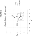
- the article exhibits an angular color shift (as described herein) of less than about 10 (e.g., 5 or less, 4 or less, 3 or less, 2 or less or about 1 or less) from a reference illumination angle to an incident illumination angle in the range from about 2 degrees to about 60 degrees, when viewed at the anti-reflective surface using an illuminant.
- exemplary illuminants include any one of CIE F2, CIE F10, CIE F11, CIE F12 and CIE D65.
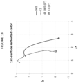
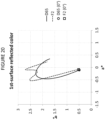
- the article may exhibit a b* value of less than about 2 in the CIE L*, a*, b* colorimetry system at all incidence illumination angles in the range from about 0 to about 60 degrees.
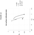
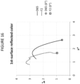
- the article of some embodiments exhibits a transmittance color (or transmittance color coordinates) and/or a reflectance color (or reflectance color coordinates) measured at the anti-reflective surface at normal incidence having a reference point color shift of less than about 2 from a reference point, as defined herein.
- the angular color shift, the reference point color shift and the color coordinates (a* and/or b*) described herein are observed under a D65 and/or F2 illuminant.
- the optical performance described herein is observed under a F2 illuminant, which is known to be more challenging due to the sharp spectral features of the F2 illuminant source.
- the anti-reflective coating may include a plurality of layers.
- the anti-reflective coating includes a period comprising a first low RI layer and a second high RI layer.
- the period may include a first low RI layer and a second high RI disposed on the first low RI layer or vice versa.
- the period may include a third layer.
- the anti-reflective coating may include a plurality of periods such that the first low RI layer and the second high RI layer alternate.
- the anti-reflective coating can include up to about 10 or 20 periods.
- the optical coating includes a scratch resistant layer. Where scratch resistant layers are included, such layers may be disposed on the anti-reflective coating. In other embodiments, the scratch resistant coating is disposed between the anti-reflective coating and the substrate. Exemplary scratch resistant layers may exhibit a maximum hardness in the range from about 8GPa to about 50GPa as measured by a Berkovitch Indenter Hardness Test, as defined herein.
- the scratch resistant layer may be disposed between the substrate and the anti-reflective coating.
- the anti-reflective coating may include a first portion and a second portion such that the scratch resistant layer is disposed between the first portion and the second portion.
- the thickness of the scratch-resistant layer may be in the range from about 200 nanometers to about 3 micrometers.
- the article may include a layer having a refractive index greater than about 1.8.
- Materials that may be utilized in that layer include SiN x , SiO x N y , Si u Al v O x N y , AlN x , AlO x N y or a combination thereof.
- the article may include an additional layer, such as an easy-to-clean coating, a diamond-like carbon (“DLC”) coating, a scratch-resistant coating or a combination thereof.
- additional layer such as an easy-to-clean coating, a diamond-like carbon (“DLC") coating, a scratch-resistant coating or a combination thereof.
- Such coatings may be disposed on the anti-reflective coating or between layers of the anti-reflective coating.
- the substrate utilized in one or more embodiments of the article can include an amorphous substrate or a crystalline substrate.
- An of an amorphous substrate includes glass that may be selected from the group consisting of soda lime glass, alkali aluminosilicate glass, alkali containing borosilicate glass and alkali aluminoborosilicate glass.
- the glass may be strengthened and may include a compressive stress (CS) layer with a surface CS of at least 250 MPa extending within the strengthened glass from a surface of the chemically strengthened glass to a depth of layer (DOL) of at least about 10 ⁇ m.
- CS compressive stress
- the article 100 may include a substrate 110, and an optical coating 120 disposed on the substrate.
- the substrate 110 includes opposing major surfaces 112, 114 and opposing minor surfaces 116, 118.
- the optical coating 120 is shown in Figure 1 as being disposed on a first opposing major surface 112; however, the optical coating 120 may be disposed on the second opposing major surface 114 and/or one or both of the opposing minor surfaces, in addition to or instead of being disposed on the first opposing major surface 112.
- the optical coating 120 forms an anti-reflective surface 122.
- the optical coating 120 includes at least one layer of at least one material.
- the term "layer" may include a single layer or may include one or more sub-layers. Such sub-layers may be in direct contact with one another. The sub-layers may be formed from the same material or two or more different materials. In one or more alternative embodiments, such sub-layers may have intervening layers of different materials disposed therebetween. In one or more embodiments a layer may include one or more contiguous and uninterrupted layers and/or one or more discontinuous and interrupted layers (i.e., a layer having different materials formed adjacent to one another).
- a layer or sub-layers may be formed by any known method in the art, including discrete deposition or continuous deposition processes. In one or more embodiments, the layer may be formed using only continuous deposition processes, or, alternatively, only discrete deposition processes.
- the thickness of the optical coating 120 may be about 1 ⁇ m or greater while still providing an article that exhibits the optical performance described herein. In some examples, the optical coating 120 thickness may be in the range from about 1 ⁇ m to about 20 ⁇ m (e.g., from about 1 ⁇ m to about 10 ⁇ m, or from about 1 ⁇ m to about 5 ⁇ m).
- the term "dispose” includes coating, depositing and/or forming a material onto a surface using any known method in the art.
- the disposed material may constitute a layer, as defined herein.
- the phrase "disposed on” includes the instance of forming a material onto a surface such that the material is in direct contact with the surface and also includes the instance where the material is formed on a surface, with one or more intervening material(s) is between the disposed material and the surface.
- the intervening material(s) may constitute a layer, as defined herein.
- the optical coating 120 includes an anti-reflective coating 130, which may include a plurality of layers (130A, 130B).
- the anti-reflective coating 130 may include a period 132 comprising two or more layers.
- the two or more layers may be characterized as having different refractive indices from each another.
- the period 132 includes a first low RI layer 130A and a second high RI layer 130B. The difference in the refractive index of the first low RI layer and the second high RI layer may be about 0.01 or greater, 0.05 or greater, 0.1 or greater or even 0.2 or greater.
- the anti-reflective coating 130 may include a plurality of periods (132).
- a single period includes include a first low RI layer 130A and a second high RI layer 130B, such that when a plurality of periods are provided, the first low RI layer 130A (designated for illustration as "L") and the second high RI layer 130B (designated for illustration as "H") alternate in the following sequence of layers: L/H/L/H or H/L/H/L, such that the first low RI layer and the second high RI layer appear to alternate along the physical thickness of the anti-reflective coating 120.
- the anti-reflective coating 130 includes three periods.
- the anti-reflective coating 130 may include up to 25 periods.
- the anti-reflective coating 130 may include from about 2 to about 20 periods, from about 2 to about 15 periods, from about 2 to about 10 periods, from about 2 to about 12 periods, from about 3 to about 8 periods, from about 3 to about 6 periods.
- the anti-reflective coating 130 may include an additional capping layer 131, which may include a lower refractive index material than the second high RI layer 130B.
- the period 132 may include one or more third layers 130C, as shown in Figure 3 .
- the third layer(s) 130C may have a low RI, a high RI or a medium RI.
- the third layer(s) 130C may have the same RI as the first low RI layer 130A or the second high RI layer 130B.
- the third layer(s) 130C may have a medium RI that is between the RI of the first low RI layer 130A and the RI of the second high RI layer 130B.
- the third layer(s) 130C may have a refractive index greater than the 2 nd high RI layer 130B.
- the third layer may be provided in the anti-reflective coating 120 in the following exemplary configurations: L third layer /H/L/H/L; H third layer /L/H/L/H; L/H/L/H/L third layer ; H/L/H/L/H third layer ; L third layer /H/L/H/L/H third layer ; H third layer /L/H/L/H/L third layer ; L third layer / L/H/L/H; H third layer / H/L/H/L; H/L/H/ L/L third layer ; L/H/L/H/H third layer ; L third layer /L/H/L/H/H third layer ; L third layer /L/H/L/H/H third layer ; H third layer //H/L/H/L/L third layer ; L/M third layer /
- L without any subscript refers to the first low RI layer and "H” without any subscript refers to the second high RI layer.
- “H third sub-layer” refers to a third layer having a high RI
- "M” refers to a third layer having a medium RI, all relative to the 1 st layer and the 2 nd layer.
- the terms “low RI”, “high RI” and “medium RI” refer to the relative values for the RI to another (e.g., low RI ⁇ medium RI ⁇ high RI).
- the term “low RI” when used with the first low RI layer or with the third layer includes a range from about 1.3 to about 1.7 or 1.75.
- the term “high RI” when used with the second high RI layer or with the third layer includes a range from about 1.7 to about 2.5 (e.g., about 1.85 or greater).
- the term “medium RI” when used with the third layer includes a range from about 1.55 to about 1.8.
- the ranges for low RI, high RI and medium RI may overlap; however, in most instances, the layers of the anti-reflective coating 130 have the general relationship regarding RI of: low RI ⁇ medium RI ⁇ high RI.
- the third layer(s) 130C may be provided as a separate layer from a period 132 and may be disposed between the period or plurality of periods and the capping layer 131, as shown in Figure 4 .
- the third layer(s) may also be provided as a separate layer from a period 132 and may have disposed between the substrate 110 and the plurality of periods 132, as shown in Figure 5 .
- the third layer(s) 130C may be used in addition to an additional coating 140 instead of the capping 131 or in addition to the capping layer, as shown in Figure 6 .
- Exemplary materials suitable for use in the anti-reflective coating 130 include: SiO 2 , Al 2 O 3 , GeO 2 , SiO, AlOxNy, AlN, SiNx, SiO x N y , Si u Al v O x N y , Ta 2 O 5 , Nb 2 O 5 , TiO 2 , ZrO 2 , TiN, MgO, MgF 2 , BaF 2 ,CaF 2 , SnO 2 , HfO 2 , Y 2 O 3 , MoO 3 , DyF 3 , YbF 3 , YF 3 , CeF 3 , polymers, fluoropolymers, plasma-polymerized polymers, siloxane polymers, silsesquioxanes, polyimides, fluorinated polyimides, polyetherimide, polyethersulfone, polyphenylsulfone, polycarbonate, polyethylene terephthalate, polyethylene naphthalate
- suitable materials for use in the first low RI layer include SiO 2 , Al 2 O 3 , GeO 2 , SiO, AlO x N y , SiO x N y , Si u Al y O x N y , MgO, MgAl 2 O 4 , MgF 2 , BaF 2 , CaF 2 , DyF 3 , YbF 3 , YF 3 , and CeF 3 .
- the nitrogen content of the materials for use in the first low RI layer may be minimized (e.g., in materials such as Al 2 O 3 and MgAl 2 O 4 ).
- suitable materials for use in the second high RI layer include Si u Al v O x N y , Ta 2 O 5 , Nb 2 O 5 , AlN, Si 3 N 4 , AlO x N y , SiO x N y , HfO 2 , TiO 2 , ZrO 2 , Y 2 O 3 , Al 2 O 3 , MoO 3 and diamond-like carbon.
- the oxygen content of the materials for the second high RI layer and/or the scratch-resistant layer may be minimized, especially in SiNx or AlNx materials.
- AlO x N y materials may be considered to be oxygen-doped AlNx, that is they may have an AlNx crystal structure (e.g.
- Exemplary preferred AlO x N y high RI materials may comprise from about 0 atom% to about 20 atom% oxygen, or from about 5 atom% to about 15 atom% oxygen, while including 30 atom% to about 50 atom% nitrogen.
- Exemplary preferred Si u Al v O x N y high RI materials may comprise from about 10 atom% to about 30 atom% or from about 15 atom% to about 25 atom% silicon, from about 20 atom% to about 40 atom% or from about 25 atom% to about 35 atom% aluminum, from about 0 atom% to about 20 atom% or from about 1 atom% to about 20 atom% oxygen, and from about 30 atom% to about 50 atom% nitrogen.
- the foregoing materials may be hydrogenated up to about 30% by weight.
- some embodiments may utilize AlN and/or SiO x N y .
- the hardness of the second high RI layer and/or the scratch-resistant layer may be characterized specifically.
- the maximum hardness of the second high RI layer and/or the scratch-resistant layer may be about 8 GPa or greater, about 10 GPa or greater, about 12 GPa or greater, about 15 GPa or greater, about 18 GPa or greater, or about 20 GPa or greater.
- the second high RI layer material may be deposited as a single layer and may be characterized as a scratch resistant layer, and this single layer may have a thickness between about 500 and 2000 nm for repeatable hardness determination.
- At least one of the layer(s) of the anti-reflective coating 130 may include a specific optical thickness range.
- the term "optical thickness” is determined by (n*d), where "n” refers to the RI of the sub-layer and “d” refers to the physical thickness of the layer.
- at least one of the layers of the anti-reflective coating 130 may include an optical thickness in the range from about 2 nm to about 200 nm, from about 10 nm to about 100 nm, from about 15 nm to about 100 nm, from about 15 to about 500 nm, or from about 15 to about 5000 nm.
- all of the layers in the anti-reflective coating 130 may each have an optical thickness in the range from about 2 nm to about 200 nm, from about 10 nm to about 100 nm, from about 15 nm to about 100 nm, from about 15 to about 500 nm, or from about 15 to about 5000 nm. In some cases, at least one layer of the anti-reflective coating 130 has an optical thickness of about 50 nm or greater.
- each of the first low RI layers have an optical thickness in the range from about 2 nm to about 200 nm, from about 10 nm to about 100 nm, from about 15 nm to about 100 nm, from about 15 to about 500 nm, or from about 15 to about 5000 nm.
- each of the second high RI layers have an optical thickness in the range from about 2 nm to about 200 nm, from about 10 nm to about 100 nm, from about 15 nm to about 100 nm, from about 15 to about 500 nm, or from about 15 to about 5000 nm.
- each of the third layers have an optical thickness in the range from about 2 nm to about 200 nm, from about 10 nm to about 100 nm, from about 15 nm to about 100 nm, from about 15 to about 500 nm, or from about 15 to about 5000 nm.
- the thickness of one or more of the layers of the optical coating 130 may be minimized. In one or more embodiments, the thickness of the thickness of the high RI layer(s) and/or the medium RI layer(s) are minimized such that they are less than about 500 nm. In one or more embodiments, the combined thickness of the high RI layer(s), the medium RI (layers) and/or the combination of the high RI and medium RI layers is less than about 500 nm.
- the amount of low RI material in the optical coating may be minimized.
- the low RI material is typically also a lower-hardness material, owing to the nature of atomic bonding and electron densities that simultaneously affect refractive index and hardness, and thus minimizing such material can maximize the hardness, while maintaining the reflectance and color performance described herein.
- the low RI material may comprise less than about 60%, less than about 50%, less than about 40%, less than about 30%, less than about 20%, less than about 10%, or less than about 5% of the physical thickness of the optical coating.
- the amount of low RI material may be quantified as the sum of the physical thicknesses of all layer of low RI material that are disposed above the thickest high RI layer in the optical coating (i.e. on the side opposite the substrate, user side or air side).
- the thick high RI layer having a high hardness effectively shields the layers underneath (or between the thick RI layer and the substrate) from many or most scratches. Accordingly, the layers disposed above the thickest high RI layer may have an outsized effect on scratch resistance of the overall article. This is especially relevant when the thickest high RI layer has a physical thickness that is greater than about 400nm and has a hardness greater than about 12 GPa as measured by the Berkovich Indenter Hardness Test.
- the amount of low RI material disposed on the thickest high RI layer may have a thickness less than or equal to about 150nm, less than or equal to about 120nm, less than or equal to about 110nm, 100nm, 90nm, 80nm, 70nm, 60nm, 50nm, 40nm, 30nm, 25nm, 20nm, 15nm, or less than or equal to about 12nm.
- the top-most air-side layer may comprise a high RI layer that also exhibits high hardness, as shown in Modeled Examples 8-9.
- an additional coating 140 may be disposed on top of this top-most air-side high RI layer (e.g., the additional coating may include low-friction coating, an oleophobic coating, or an easy-to-clean coating).
- the addition of a low RI layer having a very low thickness e.g., about 10 nm or less, about 5 nm or less or about 2 nm or less
- the low RI layer having a very low thickness may include SiO 2 , an oleophobic or low-friction layer, or a combination of SiO 2 and an oleophobic material.
- Exemplary low-friction layers may include diamond-like carbon, such materials (or one or more layers of the optical coating) may exhibit a coefficient of friction less than 0.4, less than 0.3, less than 0.2, or even less than 0.1.
- the anti-reflective coating 130 has a physical thickness of about 800 nm or less.
- the anti-reflective coating 130 may have a physical thickness in the range from about 10 nm to about 800 nm, from about 50 nm to about 800 nm, from about 100 nm to about 800 nm, from about 150 nm to about 800 nm, from about 200 nm to about 800 nm, from about 10 nm to about 750 nm, from about 10 nm to about 700 nm, from about 10 nm to about 650 nm, from about 10 nm to about 600 nm, from about 10 nm to about 550 nm, from about 10 nm to about 500 nm, from about 10 nm to about 450 nm, from about 10 nm to about 400 nm, from about 10 nm to about 350 nm, from about 10 nm to about 300 nm, from about 50 to about 300, and all range
- the combined physical thickness of the second high RI layer(s) may be characterized.
- the combined thickness of the second high RI layer(s) may be about 100 nm or greater, about 150 nm or greater, about 200 nm or greater, about 500 nm or greater.
- the combined thickness is the calculated combination of the thicknesses of the individual high RI layer(s) in the anti-reflective coating 130, even when there are intervening low RI layer(s) or other layer(s).
- the combined physical thickness of the second high RI layer(s), which may also comprise a high-hardness material (e.g., a nitride or an oxynitride material), may be greater than 30% of the total physical thickness of the anti-reflective coating.
- the combined physical thickness of the second high RI layer(s) may be about 40% or greater, about 50% or greater, about 60% or greater, about 70% or greater, about 75% or greater, or even about 80% or greater, of the total physical thickness of the anti-reflective coating.
- the amount of the high refractive index material, which may also be a high-hardness material, included in the optical coating may be characterized as a percentage of the physical thickness of the upper most (i.e., user side or side of the optical coating opposite the substrate) 500 nm of the article or optical coating 120. Expressed as a percentage of the upper most 500 nm of the article or optical coating, the combined physical thickness of the second high RI layer(s) (or the thickness of the high refractive index material) may be about 50% or greater, about 60% or greater, about 70% or greater, about 80% or greater, or even about 90% or greater.
- the second high RI layers may include a material having a refractive index greater than about 1.85 and the first low RI layers may include a material having a refractive index less than about 1.75. In some embodiments, the second high RI layers may include a nitride or an oxynitride material.
- the combined thickness of all the first low RI layers in the optical coating may be about 200 nm or less (e.g., about 150 nm or less, about 100 nm or less, about 75 nm or less, or about 50 nm or less).
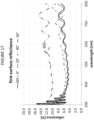
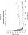
- the anti-reflective coating 130 exhibits an average light reflectance of about 9% or less, about 8% or less, about 7% or less, about 6% or less, about 5% or less, about 4% or less, about 3% or less, or about 2% or less over the optical wavelength regime, when measured at the anti-reflective surface 122 only (e.g., when removing the reflections from an uncoated back surface (e.g., 114 in Figure 1 ) of the article, such as through using index-matching oils on the back surface coupled to an absorber, or other known methods).
- the average reflectance (which may be a photopic average) may be in the range from about 0.4% to about 9%, from about 0.4% to about 8%, from about 0.4% to about 7%, from about 0.4% to about 6%, or from about 0.4% to about 5% and all ranges therebetween.
- the anti-reflective coating 120 may exhibit such average light reflectance over other wavelength ranges such as from about 450 nm to about 650 nm, from about 420 nm to about 680 nm, from about 420 nm to about 700 nm, from about 420 nm to about 740 nm, from about 420 nm to about 850 nm, or from about 420 nm to about 950 nm.
- the anti-reflective surface 122 exhibits an average light transmission of about 90% or greater, 92% or greater, 94% or greater, 96% or greater, or 98% or greater, over the optical wavelength regime.
- the average reflectance or transmittance is measured at an incident illumination angle from about 0 degrees to about 10 degrees (however, such measurements may be provided at incident illumination angles of 45 degrees or 60 degrees).
- the article 100 may include one or more additional coatings 140 disposed on the anti-reflective coating, as shown in Figure 6 .
- the additional coating may include an easy-to-clean coating.
- An example of a suitable an easy-to-clean coating is described in U.S. Patent Application No. 13/690,904, entitled “PROCESS FOR MAKING OF GLASS ARTICLES WITH OPTICAL AND EASY-TO-CLEAN COATINGS,” filed on November 30, 2012 , which is incorporated herein in its entirety by reference.
- the easy-to-clean coating may have a thickness in the range from about 5 nm to about 50 nm and may include known materials such as fluorinated silanes.
- the easy-to-clean coating may have a thickness in the range from about 1 nm to about 40 nm, from about 1 nm to about 30 nm, from about 1 nm to about 25 nm, from about 1 nm to about 20 nm, from about 1 nm to about 15 nm, from about 1 nm to about 10 nm, from about 5 nm to about 50 nm, from about 10 nm to about 50 nm, from about 15 nm to about 50 nm, from about 7 nm to about 20 nm, from about 7 nm to about 15 nm, from about 7 nm to about 12 nm or from about 7 nm to about 10 nm, and all ranges and sub-ranges therebetween.
- the first layer of diamond-like carbon may have a thickness of about 1 nm to about 20 nm or from about 4 nm to about 15 nm (or more specifically about 10 nm) and the second layer of easy-to-clean may have a thickness of about 1 nm to about 10 nm (or more specifically about 6 nm).
- the diamond-like coating may include tetrahedral amorphous carbon (Ta-C), Ta-C:H, and/or a-C-H.
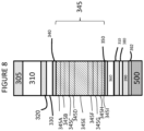
- the optical coating 120 may include a scratch resistant layer 150 or coating (when a plurality of scratch resistant layers are utilized), which may be disposed between the anti-reflective coating 130 and the substrate 110.
- the scratch resistant layer 150 or coating is disposed between the layers of the anti-reflective coating 130 (such as 150 as shown in Figure 7 or 345 as shown in Figure 8 ).
- the two sections of the anti-reflective coating i.e., a first section disposed between the scratch resistant layer 150 and the substrate 110, and a second section disposed on the scratch resistant layer
- the layers of the two sections of the anti-reflective coating may be the same in composition, order, thickness and/or arrangement as one another or may differ from one another.
- Exemplary materials used in the scratch resistant layer 150 or coating may include an inorganic carbide, nitride, oxide, diamond-like material, or combination of these.
- suitable materials for the scratch resistant layer or coating include metal oxides, metal nitrides, metal oxynitride, metal carbides, metal oxycarbides, and/or combinations thereof combination thereof.
- Exemplary metals include B, Al, Si, Ti, V, Cr, Y, Zr, Nb, Mo, Sn, Hf, Ta and W.
- the scratch resistant layer or coating may also comprise nanocomposite materials, or materials with a controlled microstructure to improve hardness, toughness, or abrasion / wear resistance.
- the scratch resistant layer or coating may comprise nanocrystallites in the size range from about 5 nm to about 30 nm.
- the scratch resistant layer or coating may comprise transformation-toughened zirconia, partially stabilized zirconia, or zirconia-toughened alumina. In embodiments, the scratch resistant layer or coating exhibits a fracture toughness value greater than about 1 MPa ⁇ m and simultaneously exhibits a hardness value greater than about 8 GPa.
- the scratch resistant layer may include a single layer 150 (as shown in Figure 7 ), multiple sub-layers or sub-layers or single layers that exhibit a refractive index gradient 345 (as shown in Figure 8 ). Where multiple layers are used, such layers form a scratch resistant coating 845.
- a scratch resistant coating 845 may include a compositional gradient of Si u Al v O x N y where the concentration of any one or more of Si, Al, O and N are varied to increase or decrease the refractive index.
- the refractive index gradient may also be formed using porosity. Such gradients are more fully described in U.S. Patent Application No. 14/262224, entitled “Scratch-Resistant Articles with a Gradient Layer", filed on April 28, 2014 , which is hereby incorporated by reference in its entirety.
- the composition of the scratch resistant layer or coating may be modified to provide specific properties (e.g., hardness).
- the scratch resistant layer or coating exhibits a maximum hardness in the range from about 5GPa to about 30GPa as measured on a major surface of the scratch resistant layer or coating, by the Berkovitch Indenter Hardness Test.
- the scratch resistant layer or coating exhibits a maximum hardness in the range from about 6 GPa to about 30 GPa, from about 7 GPa to about 30 GPa, from about 8 GPa to about 30 GPa, from about 9 GPa to about 30 GPa, from about 10 GPa to about 30 GPa, from about 12 GPa to about 30 GPa, from about 5 GPa to about 28 GPa, from about 5 GPa to about 26 GPa, from about 5 GPa to about 24 GPa, from about 5 GPa to about 22 GPa, from about 5 GPa to about 20 GPa, from about 12 GPa to about 25 GPa, from about 15 GPa to about 25 GPa, from about 16 GPa to about 24 GPa, from about 18 GPa to about 22 GPa and all ranges and sub-ranges therebetween.
- the scratch resistant coating may exhibit a maximum hardness that is greater than 15 GPa, greater than 20 GPa, or greater than 25 GPa. In one or more embodiments, the scratch resistant layer exhibits a maximum hardness in the range from about 15 GPa to about 150 GPa, from about 15 GPa to about 100 GPa, or from about 18 GPa to about 100 GPa. Maximum hardness is the highest hardness value measured over a range of indentation depths.
- Such maximum hardness values are exhibited along an indentation depth of about 50 nm or greater or 100 nm or greater (e.g., from about 100 nm to about 300 nm, from about 100 nm to about 400 nm, from about 100 nm to about 500 nm, from about 100 nm to about 600 nm, from about 200 nm to about 300 nm, from about 200 nm to about 400 nm, from about 200 nm to about 500 nm, or from about 200 nm to about 600 nm).
- the physical thickness of the scratch resistant coating or layer may be in the range from about 1 nm to about 5 ⁇ m. In some embodiments, the physical thickness of the scratch resistant coating may be in the range from about 1 nm to about 3 ⁇ m, from about 1 nm to about 2.5 ⁇ m, from about 1 nm to about 2 ⁇ m, from about 1 nm to about 1.5 ⁇ m, from about 1 nm to about 1 ⁇ m, from about 1 nm to about 0.5 ⁇ m, from about 1 nm to about 0.2 ⁇ m, from about 1 nm to about 0.1 ⁇ m, from about 1 nm to about 0.05 ⁇ m, from about 5 nm to about 0.05 ⁇ m, from about 10 nm to about 0.05 ⁇ m, from about 15 nm to about 0.05 ⁇ m, from about 20 nm to about 0.05 ⁇ m, from about 5 nm to about 0.05 ⁇ m, from about 200nm to about 3 ⁇ m, from about 400nm
- the physical thickness of the scratch resistant coating may be in the range from about 1 nm to about 25 nm.
- the scratch-resistant layer may include a nitride or an oxy-nitride material and may have a thickness of about 200nm or greater, 500nm or greater or about 1000 nm or greater.
- the article of one or more embodiments may be described as abrasion resistant as measured by various methods, after being abraded on the anti-reflective surface 122 according to a Taber Test after at least about 500 cycles.
- Various forms of abrasion test are known in the art, such as the test method specified in ASTM D1044-99, using abrasive media supplied by Taber Industries. Modified abrasion methods related to ASTM D1044-99 can be created using different types of abrading media, abradant geometry and motion, pressure, etc. in order to provide repeatable and measurable abrasion or wear tracks to meaningfully differentiate the abrasion resistance of different samples. For example, different test conditions will usually be appropriate for soft plastics vs. hard inorganic test samples.
- Taber Test refers to a test method using a Taber Linear Abraser 5750 (TLA 5750) and accessories supplied by Taber Industries, in an environment including a temperature of about 22 °C ⁇ 3 °C and Relative Humidity of up to about 70%.
- the TLA 5750 includes a CS-17 abraser material having a 6.7 mm diameter abraser head.
- each sample was abraded according to the Taber Test and the abrasive damage was evaluated using both Haze and Bidirectional Transmittance Distribution Function (CCBTDF) measurements, among other methods.
- CCBTDF Bidirectional Transmittance Distribution Function
- the procedure for abrading each sample includes placing the TLA 5750 and a flat sample support on a rigid, flat surface and securing the TLA 5750 and the sample support to the surface. Before each sample is abraded under the Taber Test, the abraser is refaced using a new S-14 refacing strip adhered to glass.
- the abraser is subjected to 10 refacing cycles using a cycle speed of 25 cycles/minute and stroke length of 1 inch, with no additional weight added (i.e., a total weight of about 350 g is used during refacing, which is the combined weight of the spindle and collet holding the abraser).
- the procedure then includes operating the TLA 5750 to abrade the sample, where the sample is placed in the sample support in contact with the abraser head and supporting the weight applied to the abraser head, using a cycle speed of 25 cycles/minute, and a stroke length of 1 inch, and a weight such that the total weight applied to the sample is 850 g (i.e., a 500 g auxiliary weight is applied in addition to the 350 g combined weight of the spindle and collet).
- the procedure includes forming two wear tracks on each sample for repeatability, and abrading each sample for 500 cycle counts in each of the two wear tracks on each sample.
- the anti-reflective surface 122 of the article 100 is abraded according to the above Taber Test and the article exhibits a haze of about 10% of less, as measured on the abraded side using a hazemeter supplied by BYK Gardner under the trademark Haze-Gard plus ® , using an aperture over the source port, the aperture having a diameter of 8 mm.
- the article 100 exhibits a haze in the range from about 0.1% to about 10%, from about 0.1% to about 9%, from about 0.1% to about 8%, from about 0.1% to about 7%, from about 0.1% to about 6%, from about 0.1% to about 5%, from about 0.1% to about 4%, from about 0.1% to about 3%, from about 0.1% to about 2%, from about 0.1% to about 1%, 0.3% to about 10%, from about 0.5% to about 10%, from about 1% to about 10%, from about 2% to about 10%, from about 3% to about 10%, from about 4% to about 10%, from about 5% to about 10%, from about 6% to about 10%, from about 7% to about 10%, from about 1% to about 8%, from about 2% to about 6%, from about 3% to about 5%, and all ranges and sub-ranges therebetween.
- article 100 abraded by the Taber Test on the anti-reflective surface 122 may exhibit an abrasion resistance as measured by atomic force microscopy (AFM) surface profiling, which may be carried out for example over an 80x80 micron area, or multiple 80x80 micron areas (to sample a larger portion of the abraded area) of the anti-reflective surface 122. From these AFM surface scans, surface roughness statistics such as RMS roughness, Ra roughness, and peak-to-valley surface height may be evaluated.
- AFM atomic force microscopy
- the article 100 may exhibit average surface roughness (Ra) values of about 50nm or less, about 25nm or less, about 12 nm or less, about 10 nm or less, or about 5 nm or less, after being abraded under the Taber Test described above.
- Ra surface roughness
- the article 100 may exhibit an abrasion resistance, after the anti-reflective surface 122 is abraded by the Taber Test as measured by a light scattering measurement.
- the light scattering measurement includes a bi-directional reflectance distribution function (BRDF) or bi-directional transmittance distribution function (BTDF) measurement carried out using a Radiant Zemax IS-SA TM instrument. This instrument has the flexibility to measure light scattering using any input angle from normal to about 85 degrees incidence in reflection, and from normal to about 85 degrees incidence in transmission, while also capturing all scattered light output in either reflection or transmission into 2*Pi steradians (a full hemisphere in reflection or transmission).
- BRDF bi-directional reflectance distribution function
- BTDF bi-directional transmittance distribution function
- the article 100 exhibits an abrasion resistance, as measured using BTDF at normal incidence and analyzing the transmitted scattered light at a selected angular range, for example from about 10° to about 80° degrees in polar angles and any angular range therein.
- the full azimuthal range of angles can be analyzed and integrated, or particular azimuthal angular slices can be selected, for example from about 0° and 90° azimuthally.
- the article 100 may exhibit a scattered light intensity as measured at the anti-reflective coating 120, of about less than about 0.1, about 0.05 or less, about 0.03 or less, about 0.02 or less, about 0.01 or less, about 0.005 or less, or about 0.003 or less (in units of 1/steradian), when using the Radiant Zemax IS-SA tool in CCBTDF mode at normal incidence in transmission, with a 2mm aperture and a monochrometer set to 600 nm wavelength, and when evaluated at polar scattering angles in the range from about 15° to about 60° (e.g. specifically, about 20° or about 40°).
- a scattered light intensity as measured at the anti-reflective coating 120 of about less than about 0.1, about 0.05 or less, about 0.03 or less, about 0.02 or less, about 0.01 or less, about 0.005 or less, or about 0.003 or less (in units of 1/steradian), when using the Radiant Zemax IS-SA tool in CCBTDF mode at normal incidence in transmission, with
- Normal incidence in transmission may be otherwise known as zero degrees in transmission, which may be denoted as 180 ° incidence by the instrument software.
- the scattered light intensity may be measured along an azimuthal direction substantially orthogonal to the abraded direction of a sample abraded by the Taber Test.
- the Taber Test may use from about 10 cycles to about 1000 cycles, and all values in between. These optical intensity values may also correspond to less than about 1%, less than about 0.5%, less than about 0.2%, or less than about 0.1% of the input light intensity that is scattered into polar scattering angles greater than about 5 degrees, greater than about 10 degrees, greater than about 30 degrees, or greater than about 45 degrees.
- BTDF testing at normal incidence is closely related to the transmission haze measurement, in that both are measuring the amount of light that is scattered in transmission through a sample (or, in this case the article 100, after abrading the anti-reflective coating 120).
- BTDF measurements provide more sensitivity as well as more detailed angular information, compared to haze measurements.
- BTDF allows measurement of scattering into different polar and azimuthal angles, for example allowing us to selectively evaluate the scattering into azimuthal angles that are substantially orthogonal to the abrasion direction in the linear Taber test (these are the angles where light scattering from linear abrasion is the highest).
- Transmission haze is essentially the integration of all scattered light measured by normal incidence BTDF into the entire hemisphere of polar angles greater than about +/- 2.5 degrees.
- the optical coating 120 and the article 100 may be described in terms of a hardness measured by a Berkovich Indenter Hardness Test.
- the "Berkovich Indenter Hardness Test” includes measuring the hardness of a material on a surface thereof by indenting the surface with a diamond Berkovich indenter.
- the Berkovich Indenter Hardness Test includes indenting the anti-reflective surface 122 of the article or the surface of the optical coating 120 (or the surface of any one or more of the layers in the anti-reflective coating) with the diamond Berkovich indenter to form an indent to an indentation depth in the range from about 50 nm to about 1000 nm (or the entire thickness of the anti-reflective coating or layer, whichever is less) and measuring the maximum hardness from this indentation along the entire indentation depth range or a segment of this indentation depth (e.g., in the range from about 100 nm to about 600 nm), generally using the methods set forth in Oliver, W.C.; Pharr, G. M.
- hardness refers to a maximum hardness, and not an average hardness.
- the measured hardness may appear to increase initially due to development of the plastic zone at shallow indentation depths and then increases and reaches a maximum value or plateau at deeper indentation depths. Thereafter, hardness begins to decrease at even deeper indentation depths due to the effect of the underlying substrate. Where a substrate having an increased hardness compared to the coating is utilized, the same effect can be seen; however, the hardness increases at deeper indentation depths due to the effect of the underlying substrate.
- the indentation depth range and the hardness values at certain indentation depth range(s) can be selected to identify a particular hardness response of the optical film structures and layers thereof, described herein, without the effect of the underlying substrate.
- the region of permanent deformation (plastic zone) of a material is associated with the hardness of the material.
- an elastic stress field extends well beyond this region of permanent deformation.
- the substrate influence on hardness occurs at deeper indentation depths (i.e., typically at depths greater than about 10% of the optical film structure or layer thickness).
- a further complication is that the hardness response requires a certain minimum load to develop full plasticity during the indentation process. Prior to that certain minimum load, the hardness shows a generally increasing trend.
- small indentation depths which also may be characterized as small loads
- small loads e.g., up to about 50 nm
- the apparent hardness of a material appears to increase dramatically versus indentation depth.
- This small indentation depth regime does not represent a true metric of hardness but instead, reflects the development of the aforementioned plastic zone, which is related to the finite radius of curvature of the indenter.
- the apparent hardness approaches maximum levels.
- the influence of the substrate becomes more pronounced as the indentation depths increase. Hardness may begin to drop dramatically once the indentation depth exceeds about 30% of the optical film structure thickness or the layer thickness.
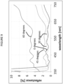
- Figure 21 illustrates the changes in measured hardness value as a function of indentation depth and thickness of a coating. As shown in Figure 21 , the hardness measured at intermediate indentation depths (at which hardness approaches and is maintained at maximum levels) and at deeper indentation depths depends on the thickness of a material or layer. Figure 21 illustrates the hardness response of four different layers of AlO x N y having different thicknesses. The hardness of each layer was measured using the Berkovich Indenter Hardness Test.
- the 500 nm-thick layer exhibited its maximum hardness at indentation depths from about 100 nm to 180 nm, followed by a dramatic decrease in hardness at indentation depths from about 180 nm to about 200 nm, indicating the hardness of the substrate influencing the hardness measurement.
- the 1000 nm-thick layer exhibited a maximum hardness at indentation depths from about 100 nm to about 300 nm, followed by a dramatic decrease in hardness at indentation depths greater than about 300 nm.
- the 1500 nm-thick layer exhibited a maximum hardness at indentation depths from about 100 nm to about 550 nm and the 2000-nm thick layer exhibited a maximum hardness at indentation depths from about 100 nm to about 600 nm.
- Figure 21 illustrates a thick single layer, the same behavior is observed in thinner coatings and those including multiple layers such as the anti-reflective coating 120 of the embodiments described herein.
- the optical 120 may exhibit a hardness of about 8 GPa or greater, about 10 GPa or greater or about 12 GPa or greater (e.g., 14 GPa or greater, 16 GPa or greater, 18 GPa or greater, 20 GPa or greater).
- the hardness of the optical coating 120 may be up to about 20 GPa or 30 GPa.
- the article 100 including the anti-reflective coating 120 and any additional coatings, as described herein, exhibit a hardness of about 5GPa or greater, about 8 GPa or greater, about 10 GPa or greater or about 12 GPa or greater (e.g., 14 GPa or greater, 16 GPa or greater, 18 GPa or greater, 20 GPa or greater), as measured on the anti-reflective surface 122, by a Berkovitch Indenter Hardness Test.
- the hardness of the optical 120 may be up to about 20 GPa or 30 GPa.
- Such measured hardness values may be exhibited by the optical coating 120 and/or the article 100 along an indentation depth of about 50 nm or greater or about 100 nm or greater (e.g., from about 100 nm to about 300 nm, from about 100 nm to about 400 nm, from about 100 nm to about 500 nm, from about 100 nm to about 600 nm, from about 200 nm to about 300 nm, from about 200 nm to about 400 nm, from about 200 nm to about 500 nm, or from about 200 nm to about 600 nm).
- the article exhibits a hardness that is greater than the hardness of the substrate (which can be measured on the opposite surface from the anti-reflective surface).
- the optical coating 120 may have at least one layer having a hardness (as measured on the surface of such layer, e.g., surface of the second high RI layer 130B of Figure 2 or the surface of the scratch resistant layer) of about 12 GPa or greater, about 13 GPa or greater, about 14 GPa or greater, about 15 GPa or greater, about 16 GPa or greater, about 17 GPa or greater, about 18 GPa or greater, about 19 GPa or greater, about 20 GPa or greater, about 22 GPa or greater, about 23 GPa or greater, about 24 GPa or greater, about 25 GPa or greater, about 26 GPa or greater, or about 27 GPa or greater (up to about 50 GPa), as measured by the Berkovich Indenter Hardness Test.
- a hardness as measured on the surface of such layer, e.g., surface of the second high RI layer 130B of Figure 2 or the surface of the scratch resistant layer
- the hardness of such layer may be in the range from about 18 GPa to about 21 GPa, as measured by the Berkovich Indenter Hardness Test. Such measured hardness values may be exhibited by the at least one layer along an indentation depth of about 50 nm or greater or 100 nm or greater (e.g., from about 100 nm to about 300 nm, from about 100 nm to about 400 nm, from about 100 nm to about 500 nm, from about 100 nm to about 600 nm, from about 200 nm to about 300 nm, from about 200 nm to about 400 nm, from about 200 nm to about 500 nm, or from about 200 nm to about 600 nm).
- the optical coating 120 or individual layers within the optical coating may exhibit an elastic modulus of about 75GPa or greater, about 80 GPa or greater or about 85 GPa or greater, as measured on the anti-reflective surface 122, by indenting that surface with a Berkovitch indenter.
- modulus values may represent a modulus measured very close to the anti-reflective surface, e.g. at indentation depths of 0 nm to about 50 nm, or it may represent a modulus measured at deeper indentation depths, e.g. from about 50 nm to about 1000nm.
- the article may exhibit a maximum hardness in the range from about 12 GPa to about 25 GPa, as measured by the Berkovich Indenter Hardness Test on the anti-reflective surface 122, or the surface of the scratch resistant coating, respectively.
- Such measured hardness values may be exhibited along an indentation depth of about 50 nm or greater or 100 nm or greater (e.g., from about 100 nm to about 300 nm, from about 100 nm to about 400 nm, from about 100 nm to about 500 nm, from about 100 nm to about 600 nm, from about 200 nm to about 300 nm, from about 200 nm to about 400 nm, from about 200 nm to about 500 nm, or from about 200 nm to about 600 nm).
- This hardness may be exhibited even when the scratch resistant layer is not disposed at or near the anti-reflective surface 122 (e.g., as shown in Figures 7 and 8 ).
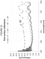
- Optical interference between reflected waves from the optical coating 120/air interface and the optical coating 120/substrate 110 interface can lead to spectral reflectance and/or transmittance oscillations that create apparent color in the article 100.
- transmittance is defined as the percentage of incident optical power within a given wavelength range transmitted through a material (e.g., the article, the substrate or the optical film or portions thereof).
- reflectance is similarly defined as the percentage of incident optical power within a given wavelength range that is reflected from a material (e.g., the article, the substrate, or the optical film or portions thereof). Transmittance and reflectance are measured using a specific linewidth.
- the spectral resolution of the characterization of the transmittance and reflectance is less than 5 nm or 0.02 eV.
- the color may be more pronounced in reflection.
- the angular color shifts in reflection with viewing angle due to a shift in the spectral reflectance oscillations with incident illumination angle.
- Angular color shifts in transmittance with viewing angle are also due to the same shift in the spectral transmittance oscillation with incident illumination angle.
- the observed color and angular color shifts with incident illumination angle are often distracting or objectionable to device users, particularly under illumination with sharp spectral features such as fluorescent lighting and some LED lighting.
- Angular color shifts in transmission may also play a factor in color shift in reflection and vice versa.
- Factors in angular color shifts in transmission and/or reflection may also include angular color shifts due to viewing angle or angular color shifts away from a certain white point that may be caused by material absorption (somewhat independent of angle) defined by a particular illuminant or test system.
- the oscillations may be described in terms of amplitude.
- the term “amplitude” includes the peak-to-valley change in reflectance or transmittance.
- the phrase “average amplitude” includes the peak-to-valley change in reflectance or transmittance averaged over several oscillation cycles or wavelength sub-ranges within the optical wavelength regime.
- the "optical wavelength regime” includes the wavelength range from about 400 nm to about 800 nm (and more specifically from about 450 nm to about 650 nm).
- the embodiments of this disclosure include an anti-reflective coating to provide improved optical performance, in terms of colorlessness and/or smaller angular color shifts with viewed at varying incident illumination angles from normal incidence under different illuminants.
- One aspect of this disclosure pertains to an article that exhibits colorlessness in reflectance and/or transmittance even when viewed at different incident illumination angles under an illuminant.
- the article exhibits an angular color shift in reflectance and/or transmittance of about 5 or less or about 2 or less between a reference illumination angle and any incidental illumination angles in the ranges provided herein.
- color shift angular or reference point
- the phrase "color shift" refers to the change in both a* and b*, under the CIE L*, a*, b* colorimetry system in reflectance and/or transmittance.
- angular color shift may be determined using the following Equation (1): ⁇ a ⁇ 2 ⁇ a ⁇ 1 2 + b ⁇ 2 ⁇ b ⁇ 1 2 , with a* 1 , and b* 1 representing the a* and b* coordinates of the article when viewed at incidence reference illumination angle (which may include normal incidence) and a* 2 , and b* 2 representing the a* and b* coordinates of the article when viewed at an incident illumination angle, provided that the incident illumination angle is different from the reference illumination angle and in some cases differs from the reference illumination angle by at least about 1 degree, 2 degrees or about 5 degrees.
- an angular color shift in reflectance and/or transmittance of about 10 or less is exhibited by the article when viewed at various incident illumination angles from a reference illumination angle, under an illuminant.
- the angular color shift in reflectance and/or transmittance is about 1.9 or less, 1.8 or less, 1.7 or less, 1.6 or less, 1.5 or less, 1.4 or less, 1.3 or less, 1.2 or less, 1.1 or less, 1 or less, 0.9 or less, 0.8 or less, 0.7 or less, 0.6 or less, 0.5 or less, 0.4 or less, 0.3 or less, 0.2 or less, or 0.1 or less.
- the angular color shift may be about 0.
- the illuminant can include standard illuminants as determined by the CIE, including A illuminants (representing tungsten-filament lighting), B illuminants (daylight simulating illuminants), C illuminants (daylight simulating illuminants), D series illuminants (representing natural daylight), and F series illuminants (representing various types of fluorescent lighting).
- the articles exhibit an angular color shift in reflectance and/or transmittance of about 2 or less when viewed at incident illumination angle from the reference illumination angle under a CIE F2, F10, F11, F12 or D65 illuminant, or more specifically, under a CIE F2 illuminant.
- the reference illumination angle may include normal incidence (i.e., from about 0 degrees to about 10 degrees), or 5 degrees from normal incidence, 10 degrees from normal incidence, 15 degrees from normal incidence, 20 degrees from normal incidence, 25 degrees from normal incidence, 30 degrees from normal incidence, 35 degrees from normal incidence, 40 degrees from normal incidence, 50 degrees from normal incidence, 55 degrees from normal incidence, or 60 degrees from normal incidence, provided the difference between the reference illumination angle and the difference between the incident illumination angle and the reference illumination angle is at least about 1 degree, 2 degrees or about 5 degrees.
- the incident illumination angle may be, with respect to the reference illumination angle, in the range from about 5 degrees to about 80 degrees, from about 5 degrees to about 70 degrees, from about 5 degrees to about 65 degrees, from about 5 degrees to about 60 degrees, from about 5 degrees to about 55 degrees, from about 5 degrees to about 50 degrees, from about 5 degrees to about 45 degrees, from about 5 degrees to about 40 degrees, from about 5 degrees to about 35 degrees, from about 5 degrees to about 30 degrees, from about 5 degrees to about 25 degrees, from about 5 degrees to about 20 degrees, from about 5 degrees to about 15 degrees, and all ranges and sub-ranges therebetween, away from the reference illumination angle.
- the article may exhibit the angular color shifts in reflectance and/or transmittance described herein at and along all the incident illumination angles in the range from about 2 degrees to about 80 degrees (or from about 10 degrees to about 80 degrees, or from about 20 degrees to about 80 degrees), when the reference illumination angle is normal incidence.
- the article may exhibit the angular color shifts in reflectance and/or transmittance described herein at and along all the incident illumination angles in the range from about 2 degrees to about 80 degrees (or from about 10 degrees to about 80 degrees, or from about 20 degrees to about 80 degrees), when the difference between the incident illumination angle and the reference illumination angle is at least about 1 degree, 2 degrees or about 5 degrees.
- the article may exhibit an angular color shift in reflectance and/or transmittance of 5 or less (e.g., 4 or less, 3 or less or about 2 or less) at any incident illumination angle in the range from about 2 degrees to about 60 degrees, from about 5 degrees to about 60 degrees, or from about 10 degrees to about 60 degrees away from a reference illumination angle equal to normal incidence.
- the article may exhibit an angular color shift in reflectance and/or transmittance of 5 or less (e.g., 4 or less, 3 or less or about 2 or less) when the reference illumination angle is 10 degrees and the incident illumination angle is any angle in the range from about 12 degrees to about 60 degrees, from about 15 degrees to about 60 degrees, or from about 20 degrees to about 60 degrees away from the reference illumination angle.
- the angular color shift may be measured at all angles between a reference illumination angle (e.g., normal incidence) and an incident illumination angle in the range from about 20 degrees to about 80 degrees.
- the angular color shift may be measured and may be less than about 5 or less than about 2, at all angles in the range from about 0 degrees and 20 degrees, from about 0 degrees to about 30 degrees, from about 0 degrees to about 40 degrees, from about 0 degrees to about 50 degrees, from about 0 degrees to about 60 degrees or from about 0 degrees to about 80 degrees.
- the article exhibits a color in the CIE L*, a*, b* colorimetry system in reflectance and/or transmittance such that the distance or reference point color shift between the transmittance color or reflectance coordinates from a reference point is less than about 5 or less than about 2 under an illuminant (which can include standard illuminants as determined by the CIE, including A illuminants (representing tungsten-filament lighting), B illuminants (daylight simulating illuminants), C illuminants (daylight simulating illuminants), D series illuminants (representing natural daylight), and F series illuminants (representing various types of fluorescent lighting)).
- illuminant which can include standard illuminants as determined by the CIE, including A illuminants (representing tungsten-filament lighting), B illuminants (daylight simulating illuminants), C il
- the articles exhibit a color shift in reflectance and/or transmittance of about 2 or less when viewed at incident illumination angle from the reference illumination angle under a CIE F2, F10, F11, F12 or D65 illuminant or more specifically under a CIE F2 illuminant.
- the article may exhibit a transmittance color (or transmittance color coordinates) and/or a reflectance color (or reflectance color coordinates) measured at the anti-reflective surface 122 having a reference point color shift of less than about 2 from a reference point, as defined herein.
- the transmittance color or transmittance color coordinates are measured on two surfaces of the article including at the anti-reflective surface 122 and the opposite bare surface of the article (i.e., 114). Unless otherwise noted, the reflectance color or reflectance color coordinates are measured on only the anti-reflective surface 122 of the article. However, the reflectance color or reflectance color coordinates described herein can be measured on both the anti-reflectiev surface 122 of the article and the opposite side of the article (i.e., major surface 114 in Figure 1 ) using either a 2-surface measurement (reflections from two sides of an article are both included) or a 1-surface measurement (reflection only from the anti-reflective surface 122 of the article is measured).
- the 1-surface reflectance measurement is typically the more challenging metric to achieve low color or low-color shift values for anti-reflective coatings, and this has relevance to applications (such as smartphones, etc.) where the back surface of the article is bonded to a light absorbing medium such as black ink or an LCD or OLED device).
- the L* coordinate of the articles described herein are the same as the reference point and do not influence color shift.
- the transmittance color coordinates of the article are compared to the transmittance color coordinates of the substrate and the reflectance color coordinates of the article are compared to the reflectance color coordinates of the substrate.
- reference point color shift ⁇ a ⁇ article + 2 2 + b ⁇ article + 2 2
- reference point color shift ⁇ a ⁇ article ⁇ a ⁇ substrate 2 + b ⁇ article ⁇ b ⁇ substrate 2
- the article may exhibit a b* value in reflectance (as measured at the anti-reflective surface only) in the range from about -5 to about 1, from about -5 to about 0, from about -4 to about 1, or from about -4 to about 0, in the CIE L*, a*, b* colorimetry system at all incidence illumination angles in the range from about 0 to about 60 degrees (or from about 0 degrees to about 40 degrees or from about 0 degrees to about 30 degrees).
- the article may exhibit a b* value in transmittance (as measured at the anti-reflective surface and the opposite bare surface of the article) of less than about 2 (or about 1.8 or less, about 1.6 or less, 1.5 or less, 1.4 or less, 1.2 or less, or about 1 or less) in the CIE L*, a*, b* colorimetry system at all incidence illumination angles in the range from about 0 to about 60 degrees (or from about 0 degrees to about 40 degrees or from about 0 degrees to about 30 degrees).
- the lower limit of the b* value in transmittance may be about -5.
- the article exhibits an a* value in transmittance (at the anti-reflective surface and the opposite bare surface) in the range from about -1.5 to about 1.5 (e.g., -1.5 to -1.2, -1.5 to -1, -1.2 to 1.2, -1 to 1, -1 to 0.5, or -1 to 0) at incident illumination angles in the range from about 0 degrees to about 60 degrees under illuminants D65, A, and F2.
- a* value in transmittance at the anti-reflective surface and the opposite bare surface in the range from about -1.5 to about 1.5 (e.g., -1.5 to -1.2, -1.5 to -1, -1.2 to 1.2, -1 to 1, -1 to 0.5, or -1 to 0) at incident illumination angles in the range from about 0 degrees to about 60 degrees under illuminants D65, A, and F2.
- the article exhibits a b* value in transmittance (at the anti-reflective surface and the opposite bare surface) in the range from about -1.5 to about 1.5 (e.g., -1.5 to -1.2, -1.5 to -1, -1.2 to 1.2, -1 to 1, -1 to 0.5, or -1 to 0) at incident illumination angles in the range from about 0 degrees to about 60 degrees under illuminants D65, A, and F2.
- a b* value in transmittance at the anti-reflective surface and the opposite bare surface in the range from about -1.5 to about 1.5 (e.g., -1.5 to -1.2, -1.5 to -1, -1.2 to 1.2, -1 to 1, -1 to 0.5, or -1 to 0) at incident illumination angles in the range from about 0 degrees to about 60 degrees under illuminants D65, A, and F2.
- the article exhibits an a* value in reflectance (at only the anti-reflective surface) in the range from about -5 to about 2 (e.g., -4.5 to 1.5, -3 to 0, -2.5 to 0.25) at incident illumination angles in the range from about 0 degrees to about 60 degrees under illuminants D65, A, and F2.
- the article exhibits a b* value in reflectance (at only the anti-reflective surface) in the range from about -7 to about 0 at incident illumination angles in the range from about 0 degrees to about 60 degrees under illuminants D65, A, and F2.
- the article of one or more embodiments, or the anti-reflective surface 122 of one or more articles may exhibit an average light transmittance of about 95% or greater (e.g., about 9.5% or greater, about 96% or greater, about 96.5% or greater, about 97% or greater, about 97.5% or greater, about 98% or greater, about 98.5% or greater or about 99% or greater) over the optical wavelength regime in the range from about 400 nm to about 800 nm.
- the article, or the anti-reflective surface 122 of one or more articles may exhibit an average light reflectance of about 2% or less (e.g., about 1.5% or less, about 1% or less, about 0.75% or less, about 0.5% or less, or about 0.25% or less) over the optical wavelength regime in the range from about 400 nm to about 800 nm.
- These light transmittance and light reflectance values may be observed over the entire optical wavelength regime or over selected ranges of the optical wavelength regime (e.g., a 100 nm wavelength range, 150 nm wavelength range, a 200 nm wavelength range, a 250 nm wavelength range, a 280 nm wavelength range, or a 300 nm wavelength range, within the optical wavelength regime).
- these light reflectance and transmittance values may be a total reflectance or total transmittance (taking into account reflectance or transmittance on both the anti-reflective surface 122 and the opposite major surface 114) or may be observed on a single side of the article, as measured on the anti-reflective surface 122 only (without taking into account the opposite surface).
- the average reflectance or transmittance is measured at an incident illumination angle in the range from about 0 degrees to about 10 degrees (however, such measurements may be provided at incident illumination angles of 45 degrees or 60 degrees).
- the article of one or more embodiments, or the anti-reflective surface 122 of one or more articles may exhibit an average visible photopic reflectance of about 1% or less, about 0.7% or less, about 0.5% or less, or about 0.45% or less over the optical wavelength regime.
- These photopic reflectance values may be exhibited at incident illumination angles in the range from about 0° to about 20°, from about 0° to about 40° or from about 0° to about 60°.
- photopic reflectance mimics the response of the human eye by weighting the reflectance versus wavelength spectrum according to the human eye's sensitivity.
- Photopic reflectance may also be defined as the luminance, or tristimulus Y value of reflected light, according to known conventions such as CIE color space conventions.
- the article exhibits a single-side average photopic reflectance, measured at normal or near-normal incidence (e.g. 0-10 degrees) on the anti-reflective surface only of less than about 10%.
- the single-side average photopic reflectance is about 9% or less, about 8% or less, about 7% or less, about 6% or less, about 5% or less, about 4% or less, about 3%, or about 2% or less.
- the anti-reflective surface 122 of one or more articles i.e.
- the anti-reflective surface only through a single-sided measurement may exhibit the above average photopic reflectance values, while simultaneously exhibiting a maximum reflectance color shift, over the entire incident illumination angle range from about 5 degrees to about 60 degrees (with the reference illumination angle being normal incidence) using D65 illumination and/or F2 illuminant, of less than about 5.0, less than about 4.0, less than about 3.0, less than about 2.0, less than about 1.5, or less than about 1.25.
- These maximum reflectance color shift values represent the lowest color point value measured at any angle from about 5 degrees to about 60 degrees from normal incidence, subtracted from the highest color point value measured at any angle in the same range.
- the values may represent a maximum change in a* value (a* highest -a* lowest ), a maximum change in b* value (b* highest -b* lowest ), a maximum change in both a* and b* values, or a maximum change in the quantity ⁇ ((a* highest -a* lowest ) 2 +(b* highest -b* lowest ) 2 ).
- the substrate 110 may include an inorganic material and may include an amorphous substrate, a crystalline substrate or a combination thereof.
- the substrate 110 may be formed from man-made materials and/or naturally occurring materials (e.g., quartz and polymers).
- the substrate 110 may be characterized as organic and may specifically be polymeric.
- suitable polymers include, without limitation: thermoplastics including polystyrene (PS) (including styrene copolymers and blends), polycarbonate (PC) (including copolymers and blends), polyesters (including copolymers and blends, including polyethyleneterephthalate and polyethyleneterephthalate copolymers), polyolefins (PO) and cyclicpolyolefins (cyclic-PO), polyvinylchloride (PVC), acrylic polymers including polymethyl methacrylate (PMMA) (including copolymers and blends), thermoplastic urethanes (TPU), polyetherimide (PEI) and blends of these polymers with each other.
- Other exemplary polymers include epoxy, styrenic, phenolic, melamine, and silicone resins.
- the substrate 110 may specifically exclude polymeric, plastic and/or metal substrates.
- the substrate may be characterized as alkali-including substrates (i.e., the substrate includes one or more alkalis).
- the substrate exhibits a refractive index in the range from about 1.45 to about 1.55.
- the substrate 110 may exhibit an average strain-to-failure at a surface on one or more opposing major surface that is 0.5% or greater, 0.6% or greater, 0.7% or greater, 0.8% or greater, 0.9% or greater, 1% or greater, 1.1% or greater, 1.2% or greater, 1.3% or greater, 1.4% or greater 1.5% or greater or even 2% or greater, as measured using ball-on-ring testing using at least 5, at least 10, at least 15, or at least 20 samples.
- the substrate 110 may exhibit an average strain-to-failure at its surface on one or more opposing major surface of about 1.2%, about 1.4%, about 1.6%, about 1.8%, about 2.2%, about 2.4%, about 2.6%, about 2.8%, or about 3% or greater.
- Suitable substrates 110 may exhibit an elastic modulus (or Young's modulus) in the range from about 30 GPa to about 120 GPa.
- the elastic modulus of the substrate may be in the range from about 30 GPa to about 110 GPa, from about 30 GPa to about 100 GPa, from about 30 GPa to about 90 GPa, from about 30 GPa to about 80 GPa, from about 30 GPa to about 70 GPa, from about 40 GPa to about 120 GPa, from about 50 GPa to about 120 GPa, from about 60 GPa to about 120 GPa, from about 70 GPa to about 120 GPa, and all ranges and sub-ranges therebetween.
- the amorphous substrate may include glass, which may be strengthened or non-strengthened.
- suitable glass include soda lime glass, alkali aluminosilicate glass, alkali containing borosilicate glass and alkali aluminoborosilicate glass.
- the glass may be free of lithia.
- the substrate 110 may include crystalline substrates such as glass ceramic substrates (which may be strengthened or non-strengthened) or may include a single crystal structure, such as sapphire.
- the substrate 110 includes an amorphous base (e.g., glass) and a crystalline cladding (e.g., sapphire layer, a polycrystalline alumina layer and/or or a spinel (MgAl 2 O 4 ) layer).
- amorphous base e.g., glass
- a crystalline cladding e.g., sapphire layer, a polycrystalline alumina layer and/or or a spinel (MgAl 2 O 4 ) layer.
- the substrate 110 of one or more embodiments may have a hardness that is less than the hardness of the article (as measured by the Berkovich Indenter Hardness Test described herein).
- the hardness of the substrate may be measured using known methods in the art, including but not limited to the Berkovich Indenter Hardness Test or Vickers hardness test.
- the substrate 110 may be substantially planar or sheet-like, although other embodiments may utilize a curved or otherwise shaped or sculpted substrate.
- the substrate 110 may be substantially optically clear, transparent and free from light scattering. In such embodiments, the substrate may exhibit an average light transmission over the optical wavelength regime of about 85% or greater, about 86% or greater, about 87% or greater, about 88% or greater, about 89% or greater, about 90% or greater, about 91% or greater or about 92% or greater.
- the substrate 110 may be opaque or exhibit an average light transmission over the optical wavelength regime of less than about 10%, less than about 9%, less than about 8%, less than about 7%, less than about 6%, less than about 5%, less than about 4%, less than about 3%, less than about 2%, less than about 1%, or less than about 0%.
- these light reflectance and transmittance values may be a total reflectance or total transmittance (taking into account reflectance or transmittance on both major surfaces of the substrate) or may be observed on a single side of the substrate (i.e., on the anti-reflective surface 122 only, without taking into account the opposite surface).
- the average reflectance or transmittance is measured at an incident illumination angle of 0 degrees (however, such measurements may be provided at incident illumination angles of 45 degrees or 60 degrees).
- the substrate 110 may optionally exhibit a color, such as white, black, red, blue, green, yellow, orange etc.
- the physical thickness of the substrate 110 may vary along one or more of its dimensions for aesthetic and/or functional reasons.
- the edges of the substrate 110 may be thicker as compared to more central regions of the substrate 110.
- the length, width and physical thickness dimensions of the substrate 110 may also vary according to the application or use of the article 100.
- the substrate 110 may be provided using a variety of different processes.
- various forming methods can include float glass processes and down-draw processes such as fusion draw and slot draw.
- a substrate 110 may be strengthened to form a strengthened substrate.
- the term "strengthened substrate” may refer to a substrate that has been chemically strengthened, for example through ion-exchange of larger ions for smaller ions in the surface of the substrate.
- other strengthening methods known in the art such as thermal tempering, or utilizing a mismatch of the coefficient of thermal expansion between portions of the substrate to create compressive stress and central tension regions, may be utilized to form strengthened substrates.
- the ions in the surface layer of the substrate are replaced by - or exchanged with - larger ions having the same valence or oxidation state.
- Ion exchange processes are typically carried out by immersing a substrate in a molten salt bath containing the larger ions to be exchanged with the smaller ions in the substrate.
- parameters for the ion exchange process including, but not limited to, bath composition and temperature, immersion time, the number of immersions of the substrate in a salt bath (or baths), use of multiple salt baths, additional steps such as annealing, washing, and the like, are generally determined by the composition of the substrate and the desired compressive stress (CS), depth of compressive stress layer (or depth of layer) of the substrate that result from the strengthening operation.
- CS compressive stress
- depth of compressive stress layer or depth of layer of the substrate that result from the strengthening operation.
- ion exchange of alkali metal-containing glass substrates may be achieved by immersion in at least one molten bath containing a salt such as, but not limited to, nitrates, sulfates, and chlorides of the larger alkali metal ion.
- the temperature of the molten salt bath typically is in a range from about 380°C up to about 450°C, while immersion times range from about 15 minutes up to about 40 hours. However, temperatures and immersion times different from those
- the degree of chemical strengthening achieved by ion exchange may be quantified based on the parameters of central tension (CT), surface CS, and depth of layer (DOL).
- CT central tension
- surface CS may be measured near the surface or within the strengthened glass at various depths.
- a maximum CS value may include the measured CS at the surface (CS s ) of the strengthened substrate.
- the CT which is computed for the inner region adjacent the compressive stress layer within a glass substrate, can be calculated from the CS, the physical thickness t, and the DOL.
- CS and DOL are measured using those means known in the art. Such means include, but are not limited to, measurement of surface stress (FSM) using commercially available instruments such as the FSM-6000, manufactured by Luceo Co., Ltd.
- CT CS ⁇ DOL / t ⁇ 2 DOL
- t is the physical thickness ( ⁇ m) of the glass article.
- CT and CS are expressed herein in megaPascals (MPa)
- physical thickness t is expressed in either micrometers ( ⁇ m) or millimeters (mm)
- DOL is expressed in micrometers ( ⁇ m).
- a strengthened substrate 110 can have a surface CS of 250 MPa or greater, 300 MPa or greater, e.g., 400 MPa or greater, 450 MPa or greater, 500 MPa or greater, 550 MPa or greater, 600 MPa or greater, 650 MPa or greater, 700 MPa or greater, 750 MPa or greater or 800 MPa or greater.
- the strengthened substrate may have a DOL of 10 ⁇ m or greater, 15 ⁇ m or greater, 20 ⁇ m or greater (e.g., 25 ⁇ m, 30 ⁇ m, 35 ⁇ m, 40 ⁇ m, 45 ⁇ m, 50 ⁇ m or greater) and/or a CT of 10 MPa or greater, 20 MPa or greater, 30 MPa or greater, 40 MPa or greater (e.g., 42 MPa, 45 MPa, or 50 MPa or greater) but less than 100 MPa (e.g., 95, 90, 85, 80, 75, 70, 65, 60, 55 MPa or less).
- the strengthened substrate has one or more of the following: a surface CS greater than 500 MPa, a DOL greater than 15 ⁇ m, and a CT greater than 18 MPa.
- Example glasses that may be used in the substrate may include alkali aluminosilicate glass compositions or alkali aluminoborosilicate glass compositions, though other glass compositions are contemplated. Such glass compositions are capable of being chemically strengthened by an ion exchange process.
- One example glass composition comprises SiO 2 , B 2 O 3 and Na 2 O, where (SiO 2 + B 2 O 3 ) ⁇ 66 mol. %, and Na 2 O ⁇ 9 mol. %.
- the glass composition includes at least 6 wt.% aluminum oxide.
- the substrate includes a glass composition with one or more alkaline earth oxides, such that a content of alkaline earth oxides is at least 5 wt.%.
- Suitable glass compositions in some embodiments, further comprise at least one of K 2 O, MgO, and CaO.
- the glass compositions used in the substrate can comprise 61-75 mol.% SiO2; 7-15 mol.% Al 2 O 3 ; 0-12 mol.% B 2 O 3 ; 9-21 mol.% Na 2 O; 0-4 mol.% K 2 O; 0-7 mol.% MgO; and 0-3 mol.% CaO.
- a further example glass composition suitable for the substrate comprises: 60-70 mol.% SiO 2 ; 6-14 mol.% Al 2 O 3 ; 0-15 mol.% B 2 O 3 ; 0-15 mol.% Li 2 O; 0-20 mol.% Na 2 O; 0-10 mol.% K 2 O; 0-8 mol.% MgO; 0-10 mol.% CaO; 0-5 mol.% ZrO 2 ; 0-1 mol.% SnO 2 ; 0-1 mol.% CeO 2 ; less than 50 ppm As 2 O 3 ; and less than 50 ppm Sb 2 O 3 ; where 12 mol.% ⁇ (Li 2 O + Na 2 O + K 2 O) ⁇ 20 mol.% and 0 mol.% ⁇ (MgO + CaO) ⁇ 10 mol.%.
- a still further example glass composition suitable for the substrate comprises: 63.5-66.5 mol.% SiO 2 ; 8-12 mol.% Al 2 O 3 ; 0-3 mol.% B 2 O 3 ; 0-5 mol.% Li 2 O; 8-18 mol.% Na 2 O; 0-5 mol.% K 2 O; 1-7 mol.% MgO; 0-2.5 mol.% CaO; 0-3 mol.% ZrO 2 ; 0.05-0.25 mol.% SnO 2 ; 0.05-0.5 mol.% CeO 2 ; less than 50 ppm As 2 O 3 ; and less than 50 ppm Sb 2 O 3 ; where 14 mol.% ⁇ (Li 2 O + Na 2 O + K 2 O) ⁇ 18 mol.% and 2 mol.% ⁇ (MgO + CaO) ⁇ 7 mol.%.
- an alkali aluminosilicate glass composition suitable for the substrate comprises alumina, at least one alkali metal and, in some embodiments, greater than 50 mol.% SiO 2 , in other embodiments at least 58 mol.% SiO 2 , and in still other embodiments at least 60 mol.% SiO 2 , wherein the ratio (Al 2 O 3 + B 2 O 3 )/ ⁇ modifiers (i.e., sum of modifiers) is greater than 1, where in the ratio the components are expressed in mol.% and the modifiers are alkali metal oxides.
- This glass composition in particular embodiments, comprises: 58-72 mol.% SiO 2 ; 9-17 mol.% Al 2 O 3 ; 2-12 mol.% B 2 O 3 ; 8-16 mol.% Na 2 O; and 0-4 mol.% K 2 O, wherein the ratio (Al 2 O 3 + B 2 O 3 )/ ⁇ modifiers (i.e., sum of modifiers) is greater than 1.
- the substrate may include an alkali aluminosilicate glass composition comprising: 64-68 mol.% SiO 2 ; 12-16 mol.% Na 2 O; 8-12 mol.% Al 2 O 3 ; 0-3 mol.% B 2 O 3 ; 2-5 mol.% K 2 O; 4-6 mol.% MgO; and 0-5 mol.% CaO, wherein: 66 mol.% ⁇ SiO 2 + B 2 O 3 + CaO ⁇ 69 mol.%; Na 2 O + K 2 O + B 2 O 3 + MgO + CaO + SrO > 10 mol.%; 5 mol.% ⁇ MgO + CaO + SrO ⁇ 8 mol.%; (Na 2 O + B 2 O 3 ) - Al 2 O 3 ⁇ 2 mol.%; 2 mol.% ⁇ Na 2 O - Al 2 O 3 ⁇ 6 mol.%; and 4 mol.% ⁇ (Na 2 O + K 2 ; 64-
- the substrate may comprise an alkali aluminosilicate glass composition comprising: 2 mol% or more of Al 2 O 3 and/or ZrO 2 , or 4 mol% or more of Al 2 O 3 and/or ZrO 2 .
- the substrate 110 may include a single crystal, which may include Al 2 O 3 .
- Such single crystal substrates are referred to as sapphire.
- Other suitable materials for a crystalline substrate include polycrystalline alumina layer and/or spinel (MgAl 2 O 4 ).
- the crystalline substrate 110 may include a glass ceramic substrate, which may be strengthened or non-strengthened.
- suitable glass ceramics may include Li 2 O-Al 2 O 3 -SiO 2 system (i.e. LAS-System) glass ceramics, MgO-Al 2 O 3 -SiO 2 system (i.e. MAS-System) glass ceramics, and/or glass ceramics that include a predominant crystal phase including ⁇ -quartz solid solution, ⁇ -spodumene ss, cordierite, and lithium disilicate.
- the glass ceramic substrates may be strengthened using the chemical strengthening processes disclosed herein.
- MAS-System glass ceramic substrates may be strengthened in Li 2 SO 4 molten salt, whereby an exchange of 2Li + for Mg 2+ can occur.
- the substrate 110 can have a physical thickness ranging from about 100 ⁇ m to about 5 mm.
- Example substrate 110 physical thicknesses range from about 100 ⁇ m to about 500 ⁇ m (e.g., 100, 200, 300, 400 or 500 ⁇ m). Further example substrate 110 physical thicknesses range from about 500 ⁇ m to about 1000 ⁇ m (e.g., 500, 600, 700, 800, 900 or 1000 ⁇ m).
- the substrate 110 may have a physical thickness greater than about 1 mm (e.g., about 2, 3, 4, or 5 mm). In one or more specific embodiments, the substrate 110 may have a physical thickness of 2 mm or less or less than 1 mm.
- the substrate 110 may be acid polished or otherwise treated to remove or reduce the effect of surface flaws.
- the anti-reflective coating 130 may include a plurality of layers such that one or more layers may be disposed on the opposite side of the substrate 110 from the anti-reflective coating 130 (i.e., on major surface 114)( shown in Figure 1 ).
- the physical thickness of the anti-reflective coating 130 disposed on the major surface 114 may be in the range from about 0.1 ⁇ m to about 5 ⁇ m. In some instances, the physical thickness of the anti-reflective coating 140 disposed on major surface 114 may be in the range from about 0.01 ⁇ m to about 0.9 ⁇ m, from about 0.01 ⁇ m to about 0.8 ⁇ m, from about 0.01 ⁇ m to about 0.7 ⁇ m, from about 0.01 ⁇ m to about 0.6 ⁇ m, from about 0.01 ⁇ m to about 0.5 ⁇ m, from about 0.01 ⁇ m to about 0.4 ⁇ m, from about 0.01 ⁇ m to about 0.3 ⁇ m, from about 0.01 ⁇ m to about 0.2 ⁇ m, from about 0.01 ⁇ m to about 0.1 ⁇ m, from about 0.02 ⁇ m to about 1 ⁇ m, from about 0.03 ⁇ m to about 1 ⁇ m, from about 0.04 ⁇ m to about 1 ⁇ m, from about 0.05 ⁇ m to about 1
- Example A Example B
- Example C Layer Material Refractiv e Index Physical Thickness (nm) Refractiv e Index Physical Thicknes s (nm) Refractiv e Index Physical Thicknes s (nm) Medium Air 1 1 1 12 SiO2 1.46929 91.46 1.46929 83.02 1.43105 79.41 11 AlO x N y 1.97879 154.26 1.97879 152.94 1.97879 159.84 10 SiO2 1.46929 21.74 1.46929 27.14 1.43105 26.53 9 AlO x N y 1.97879 51.85 1.97879 49.8 1.97879 51.67 8 SiO2 1.46929 14.03 1.46929 17.12 1.43105 15.47 7 AlO x N y 1.97879 2000 1.97879 2000 1.97879 2000 6 SiO2 1.46929 8.51 1.46929 8.51 1.43
- Example J Example K Example L Layer Material Refractiv e Index Physical Thickness (nm) Refractiv e Index Physical Thicknes s (nm) Refractiv e Index Physical Thicknes s (nm) Medium Air 1 1 1 16 SiO2 1.46929 91.07 1.46929 91.28 1.47079 88.31 15 AlO x N y 1.97879 163.1 1.97879 163.28 1.95183 157.24 14 SiO2 1.46929 9.33 1.46929 9.01 1.47079 7.14 13 AlO x N y 1.97879 96.4 1.97879 97.14 1.95183 108.17 12 SiO2 1.46929 24.03 1.46929 23.95 1.47079 27.86 11 AlO x N y 1.97879 41.3 1.97879 41.26 1.95183 31.47 10 SiO2 1.46929 47.23 1.46929 46.9 1.47079 63.22 9 AlO x N y 1.97879 38.69 1.97879 38.64
- the physical thickness of the layers of the optical film may vary, with the scratch resistant layer (layer 6) having the greatest thickness.
- the physical thickness ranges for the layers may be as shown in Tables 3-4.
- layer 7 has the greatest physical thickness and imparts significant hardness and scratch resistance to the optical coating and the article. It should be understood that a different layer could be made to have the greatest physical thickness.
- the impedance matching layers above and below the thickest layer in this case, layer 7) mean that there is a large optical design freedom for adjusting the thickness of the thickest layer, as shown in Tables 3-4 below.
- Table 3 Layer thickness range for exemplary 12-layer optical coating.
- Table 4 Layer thickness range for exemplary 16-layer optical coatings.
- a second aspect of this disclosure pertains to a method for forming the articles described herein.
- the method includes providing a substrate having a major surface in a coating chamber, forming a vacuum in the coating chamber, forming a durable optical coating as described herein on the major surface, optionally forming an additional coating comprising at least one of an easy-to-clean coating and a scratch resistant coating, on the optical coating, and removing the substrate from the coating chamber.
- the optical coating and the additional coating are formed in either the same coating chamber or without breaking vacuum in separate coating chambers.
- the method may include loading the substrate on carriers which are then used to move the substrate in and out of different coating chambers, under load lock conditions so that a vacuum is preserved as the substrate is moved.
- the optical coating 120 and/or the additional coating 140 may be formed using various deposition methods such as vacuum deposition techniques, for example, chemical vapor deposition (e.g., plasma enhanced chemical vapor deposition (PECVD), low-pressure chemical vapor deposition, atmospheric pressure chemical vapor deposition, and plasma-enhanced atmospheric pressure chemical vapor deposition), physical vapor deposition (e.g., reactive or nonreactive sputtering or laser ablation), thermal or e-beam evaporation and/or atomic layer deposition.
- PECVD plasma enhanced chemical vapor deposition
- low-pressure chemical vapor deposition e.g., low-pressure chemical vapor deposition, atmospheric pressure chemical vapor deposition, and plasma-enhanced atmospheric pressure chemical vapor deposition
- physical vapor deposition e.g., reactive or nonreactive sputtering or laser ablation
- thermal or e-beam evaporation and/or atomic layer deposition e.g., reactive or nonreactive sputtering or
- the method may include controlling the thickness of the optical coating 120 and/or the additional coating 140 so that it does not vary by more than about 4% along at least about 80% of the area of the anti-reflective surface 122 or from the target thickness for each layer at any point along the substrate area. In some embodiments, the thickness of the optical coating 120 and/or the additional coating 140 so that it does not vary by more than about 4% along at least about 95% of the area of the anti-reflective surface 122.
- Example 1 included a 12-layer optical coating 300, including layers 305, 310, 320, 330, 340, 350, 360, 370, 380, 390 and 400 sequentially disposed on top of one another, and disposed on a strengthened aluminosilicate glass substrate 201 having a nominal composition of about 58 mol% SiO 2 , 16.5 mol% Al 2 O 3 , 17mol% Na 2 O, 3 mol% MgO, and about 6.5 mol% P 2 O 5 .
- the optical coating 300 also includes a scratch resistant layer 345 (including sub-layers 345A-345I) disposed within the layers of the anti-reflective coating.
- the structure of the article is shown in Figure 8 (the thicknesses shown in Figure 8 are not exact and intended to be illustrative) and the relative thicknesses of the layers are shown in Table 5.
- SiO 2 and Si u Al v O x N y layers were made by reactive sputtering in an AJA-Industries Sputter Deposition Tool.
- SiO 2 was deposited by DC reactive sputtering from an Si target with ion assist;
- Si u Al v O x N y material was deposited by DC reactive sputtering combined with RF superimposed DC sputtering with ion assist.
- the targets were 3" diameter Silicon and 3" diameter Al.
- the reactive gasses were nitrogen and oxygen, and the "working" (or inert) gas was Argon.
- the power supplied to the Silicon was radio frequency (RF) at 13.56 Mhz.
- the power supplied to the Aluminum was DC.
- Layers 340 and 345A-I of period 3 included a layer having a substantially homogenous composition (layer 340) and plurality of layers, when compared to one another, having a refractive index gradient (layers 345A-345I) formed from altering the composition of the plurality of layers from one layer to the next adjacent layer so the refractive index increases step-wise or monotonically from 2.015 to 2.079 to 2.015, as shown in Table 5.
- the refractive indices of layers 345B-D and 345F-H were not measured but were estimated based on known methods in the art.
- Example 1 The article fabricated according to Example 1 exhibited significantly improved abrasion resistance compared to the abrasion and scratch resistance of a comparative uncoated bare glass substrate together with reflectance below 1% over a portion of the optical wavelength regime.
- Table 5 Structure of Example 1.
- Modeled Examples 2-3 used modeling to demonstrate the reflectance spectra of articles that included embodiments of the optical coating, as described herein.
- the optical coating included Si u Al v O x N y and SiO 2 layers, and a strengthened aluminosilicate glass substrate having a nominal composition of about 58 mol% SiO 2 , 17 mol% Al 2 O 3 , 17 mol% Na 2 O, 3 mol% MgO, 0.1 mol% SnO, and 6.5 mol% P 2 O 5 .
- each coating material was formed onto silicon wafers by DC, RF or RF superimposed DC reactive sputtering from a silicon, aluminum, silicon and aluminum combined or co-sputtered, or magnesium fluoride target (respectively) at a temperature of about 50 °C using ion assist.
- the wafer was heated to 200 °C during deposition of some layers and targets having a 3 inch diameter were used.
- Reactive gases used included nitrogen, fluorine and oxygen; argon was used as the inert gas.
- the RF power was supplied to the silicon target at 13.56 Mhz and DC power was supplied to the Si target, Al target and other targets.
- the refractive indices (as a function of wavelength) of each of the formed layers and the glass substrate were measured using spectroscopic ellipsometry. The refractive indices thus measured were then used to calculate reflectance spectra for Modeled Examples 2-5.
- the modeled examples use a single refractive index value in their descriptive tables for convenience, which corresponds to a point selected from the dispersion curves at about 550 nm wavelength.
- Modeled Example 2 included a 12-layer optical coating with layers sequentially disposed on top of one another, disposed on a strengthened aluminosilicate glass substrate 200, as shown in Table 7.
- Table 7 Structure of Modeled Example 2.
- Layer Periods Material Refractive Index @ 550 nm Modeled Physical Thickness Ambient medium - Air 1 optical reflective coating 1 SiO 2 -a 1.4826 87 nm Si u Al v O x N y 2.015 149 nm 2 SiO 2 -a 1.4826 20 nm Si u Al v O x N y 2.015 50 nm SiO 2 -a 1.4826 12 nm Scratch resistant layer Si u Al v O x N y 2.015 505 nm (but variable in the range from about 100 nm to about 5000 nm) 3 SiO 2 -a 1.4826 9 nm Si u Al v O x N y 2.015 48 nm 4 SiO 2 -a 1.48
- the reflectance of a single side of the article of Modeled Example 2 was calculated at different viewing incident illumination angles or angle of illumination ("AOI") and the resulting reflectance spectra is shown in Figure 9 .
- the reflected color, based on a 10° observer under a D65 illuminant and a F2 illuminant was also measured and the a* and b* values are plotted as the incident illumination angle or AOI changed from 0 degrees to about 60 degrees from normal incidence at regular increments.
- the plot showing the reflected color is shown in Figure 10 .
- Modeled Example 3 included a 10-layer optical coating with layers sequentially disposed on top of one another, disposed on a strengthened aluminosilicate glass substrate 200. The relative thicknesses of the layers are shown in Table 8. Table 18: Structure of Modeled Example 3.
- the reflectance of a single side of the article of Modeled Example 3 was calculated at different viewing incident illumination angles or angle of illumination ("AOI") and the resulting reflectance spectra is shown in Figure 11 .
- the reflected color, based on a 10° observer under a D65 illuminant and a F2 illuminant was also measured and the a* and b* values are plotted as the incident illumination angle or AOI changed from 0 degrees to about 60 degrees from normal incidence at regular increments.
- the plot showing the reflected color is shown in Figure 12 .
- Modeled Examples 3 were compared to Comparative Modeled Example 4, which included a 6-layer anti-reflective coating of alternating Nb 2 O 5 and SiO 2 layers and a hydrophobic coating disposed on the anti-reflective coating.
- Comparative Modeled Example 4 ion-assisted e-beam deposition was used to deposit a single layer of Nb 2 O 5 onto a silicon wafer and a single layer of SiO 2 onto a silicon wafer.
- the refractive indices as a function of wavelength for these layers were measured using spectroscopic ellipsometry. The measured refractive indices were then used in Comparative Modeled Example 4.
- the optical performance evaluated includes average reflectance over the wavelength range from about 450 nm to about 650 nm and color shift (with reference to a* and b* coordinates (-1, -1), using the equation ⁇ ((a* example -(-1)) 2 +(b* example -(-1)) 2 )) when viewed at an incident illumination angles in the range from about 0 degrees to about 60 degrees from normal incidence under F02 and D65 illuminants.
- Table 9 shows the average reflectance and the greatest color shift of Modeled Example 3, and Comparative Modeled Example 4.
- Table 9 Average Reflectance and Color Shift for Modeled Example 3and Comparative Modeled Example 4. Ex. Avg.
- Modeled Example 3 had significantly less color shift though, although reflectance was increased slightly. Based on fabrication and testing of similar coatings with similar materials, it is believed that Modeled Example 3 would have exhibited superior scratch and abrasion resistance over Comparative Modeled Example 4.
- Example 5 included a strengthened aluminosilicate glass substrate having a nominal composition of about 58 mol% SiO 2 , 17 mol% Al 2 O 3 , 17 mol% Na 2 O, 3 mol% MgO, 0.1 mol% SnO, and 6.5 mol% P 2 O 5 and a 16-layer optical coating including a 2 micrometer scratch resistant layer, as show in Table 10.
- Table 10 Structure of Example 5.
- Example 5 exhibited a single side photopic average reflectance (i.e., measured from the anti-reflective surface 122) over the optical wavelength regime under D65 illumination at incident illumination angles of 0 °, 30°, 45 ° and 60 °, of 0.71%, 0.76%, 1.43%, and 4.83%, respectively.
- Example 5 exhibited a single side photopic average transmittance (i.e., measured through the anti-reflective surface 122) over the optical wavelength regime under D65 illumination at incident illumination angles of 0 °, 30 °, 45 ° and 60 °, of 99.26%, 99.21%, 98.54%, and 95.14%, respectively.
- Example 5 exhibited a total photopic average reflectance (i.e., measured from the anti-reflective surface 122 and the opposite major surface 114) over the optical wavelength regime under D65 illumination at incident illumination angles of 0 °, 30°, 45 ° and 60 °, of 4.80%, 4.99%, 6.36%, and 12.64%, respectively.
- Example 5 exhibited a total photopic average transmittance (i.e., measured through the anti-reflective surface 122 and the opposite major surface 114) over the optical wavelength regime under D65 illumination at incident illumination angles of 0 °, 30 °, 45 ° and 60 °, of 95.18%, 94.99%, 93.61%, and 87.33%, respectively.
- the reflectance and transmitted color coordinates for a single surface (i.e., anti-reflective surface 122) and two surfaces (i.e., anti-reflective surface 122 and major surface 114, of Figure 1 ) of Example 5, under incident illumination angles or AOI from 0 degrees to 60 degrees and illuminants D65 and F2 are shown in Tables 11A-11D.
- Single surface color coordinates were measured by eliminating transmission or reflectance from the major surface 114, as is known in the art.
- Table 11A One surface reflectance and transmitted color coordinates (Y, L*, a* and b*) using illuminant D65 for Example 5.
- Example 6 included the same strengthened aluminosilicate glass substrate as Example 5 and a coating a 12-layer optical coating including a 2 micrometer scratch resistant layer, as show in Table 12.
- Table 12 Structure of Example 6. Coating/Layer Periods, if applicable Material Refractive Index (at 550nm) Physical Thickness (nm) Ambient medium - Air Optical coating 1 SiO 2 1.46929 91.46 AlO x N y 1.97879 154.26 2 SiO 2 1.46929 21.74 AlO x N y 1.97879 51.85 SiO 2 1.46929 14.03 Scratch-Resistant Layer AlO x N y 1.97879 2000 1 SiO 2 1.46929 8.51 AlO x N y 1.97879 43.16 2 SiO 2 1.46929 28.82 AlO x N y 1.97879 25.49 3 SiO 2 1.46929 49.24 AlO x N y 1.97879 8.49 - - AS Glass 1.50542 Total coating thickness 24
- Example 6 exhibited a single side photopic average reflectance (i.e., measured from the anti-reflective surface 122) over the optical wavelength regime under D65 illumination at incident illumination angles of 0 °, 30°, 45 ° and 60 °, of 0.73%, 0.80%, 1.47%, and 4.85%, respectively.
- Example 6 exhibited a single side photopic average transmittance (i.e., measured through the anti-reflective surface 122) over the optical wavelength regime under D65 illumination at incident illumination angles of 0 °, 30 °, 45 ° and 60 °, of 99.26%, 99.18%, 98.52%, and 95.13%, respectively.
- Example 6 exhibited a total photopic average reflectance (i.e., measured from the anti-reflective surface 122 and the opposite major surface 114) over the optical wavelength regime under D65 illumination at incident illumination angles of 0 °, 30°, 45 ° and 60 °, of 4.74%, 4.94%, 6.32%, and 12.56%, respectively.
- Example 6 exhibited a total photopic average transmittance (i.e., measured through the anti-reflective surface 122 and the opposite major surface 114) over the optical wavelength regime at incident illumination angles of 0 °, 30 °, 45 ° and 60 °, of 95.24%, 95.04%, 93.67%, and 87.42%, respectively.
- the reflectance and transmitted color coordinates for a single surface (i.e., anti-reflective surface 122) and two surfaces (i.e., anti-reflective surface 122 and major surface 114, of Figure 1 ) of Example 6, under incident illumination angles or AOI from 0 degrees to 60 degrees and illuminants D65 and F2 are shown in Tables 13A-13D, in the same manner as Example 5.
- the color shift is also calculated in the same manner as Example 5.
- Table 13A One surface reflectance and transmitted color coordinates (Y, L*, a* and b*) using illuminant D65 for Example 6.
- Example 7 included the same strengthened aluminosilicate glass substrate as Example 5 and a coating a 12-layer optical coating including a 2 micrometer scratch resistant layer, as show in Table 14.
- Modeled Examples 8-11 used modeling to demonstrate the reflectance spectra of articles that included embodiments of a durable and scratch-resistant optical coating, as described herein.
- the optical coating included AlO x N y and SiO 2 layers, and a strengthened aluminosilicate glass substrate having a nominal composition of about 58 mol% SiO 2 , 17 mol% Al 2 O 3 , 17 mol% Na 2 O, 3 mol% MgO, 0.1 mol% SnO, and 6.5 mol% P 2 O 5 , as shown in Tables 15-19.
- Refractive index dispersion curves for coating materials and substrate used for Modeled Examples 8-11 were obtained in a similar manner as Modeled Examples 2-5.
- Table 15 Structure of Modeled Example 8. Coating/Layer Periods, if applicable Material Refractive Index (at 550nm) Physical Thickness (nm) Ambient medium - Air 1 1 AlO x N y 2.00605 32 SiO 2 1.48114 12 Scratch-Resistant Layer AlO x N y 2.00605 2000 Optical coating 1 SiO 2 1.48114 8.78 AlO x N y 2.00605 44.19 2 SiO 2 1.48114 32.41 AlO x N y 2.00605 24.3 3 SiO 2 1.48114 58.55 AlO x N y 2.00605 7.47 - - AS Glass 1.50542 Total coating thickness (nm) 2219.7 Table 16: Structure of Modeled Example 9.
- Figures 13-14 show the calculated reflectance spectra and the calculated reflected color, respectively, for only the anti-reflective surface of Modeled Example 8.
- Figures 15-16 show the calculated reflectance spectra and the calculated reflected color, respectively, for only the anti-reflective surface of Modeled Example 9.
- Figures 17-18 show the calculated reflectance spectra and the calculated reflected color, respectively, for only the anti-reflective surface of Modeled Example 10.
- Modeled Examples 8-11 The optical performance of Modeled Examples 8-11 is summarized in Table 22.
- Modeled Example Anti-reflective surface reflectance, photopic average (%) (single side) Maximum angular color shift, viewing angles 0-60 degrees, D65 or F2, sample referenced to itself Amount of low-index material on air-side of thickest high-index hard layer (nm) Thickness of top-most (user side) low index (e.g. SiO 2 ) layer (nm) Amount of high-index material in top 500 nm of coated article (%) 8 7.85 1.1 12 0 97.6 9 4.9 2.7 25 0 95.0 10 4.9 3.0 27 2 94.6 11 1.3 2.2 115 100 77.0
- Modeled Examples 8-11 exhibit low reflectance (i.e., values less than about 10% and less than about 8%), for viewing angles of 8°, 20°, and 40°, with the reflectance for a viewing angle of 60° being slightly higher, over the optical wavelength regime.
- Modeled Example 11 exhibited very low reflectance for viewing angles of 8°, 20°, 40° and 60° (e.g., a maximum average reflectance of about 7% or less). At viewing angles of 8°, 20°, and 40°, the average reflectance is even lower (i.e., less than about 2%).
- Modeled Examples 8 and 11 exhibited a reflected color, at viewing angles from normal incidence to 60°, of less than about 2 for both D65 and F2 illuminants.
- Modeled Example 9 and 10 exhibited a range of reflected color, at viewing angles from normal incidence to 60°, of less than about 3 for both D65 and F2 illuminants.
- Examples 8-11 also exhibit the hardness values described herein, as measured by the Berkovich Indenter Hardness Test (and, in particular, a hardness in the range from about 14 GPa to about 21 GPa).
- Modeled Examples 8-11 The optical performance of Modeled Examples 8-11 was compared to Modeled Comparative Example 4.
- the optical performance evaluated includes average reflectance over the wavelength range from about 450 nm to about 650 nm and color shift (with reference to a* and b* coordinates (-1, -1), using the equation ⁇ ((a* example -(-1)) 2 +(b* example -(-1)) 2 )) when viewed at an incident illumination angles in the range from about 0 degrees to about 60 degrees from normal incidence under F02 and D65 illuminants.
- Modeled Comparative Example 4 exhibited a lower average reflectance, but also exhibited a significantly greater color shift along viewing angles from 0 degrees to 60 degrees.
- Example 12 included a 16-layer optical coating as shown in Table 23, including layers sequentially disposed on top of one another, and disposed on a strengthened aluminosilicate glass substrate having a nominal composition of about 65 mol% SiO 2 , 5 mol% B 2 O 3 , 14 mol% Al 2 O 3 , 14 mol% Na 2 O, and 2.5 mol% MgO.
- Table 23 Structure of Example 12.
- SiO 2 and Si u Al v O x N y layers were made by reactive sputtering in an AJA-Industries Sputter Deposition Tool.
- SiO 2 was deposited by DC reactive sputtering from an Si target with ion assist;
- Si u Al v O x N y material was deposited by DC reactive sputtering combined with RF superimposed DC sputtering with ion assist.
- the targets were 3" diameter Silicon and 3" diameter Al.
- the reactive gasses were nitrogen and oxygen, and the "working" (or inert) gas was Argon.
- the power supplied to the Silicon was radio frequency (RF) at 13.56 Mhz.
- the power supplied to the Aluminum was DC.
- Example 12 The sputtering process conditions used to form the optical coating of Example 12 are shown in Table 23.
- Table 24 Sputtering Process Conditions for Example 12.
- Example 13 exhibited the optical properties shown in Table 22 and Table 23.
- Table 22 shows the reflected and transmitted color was measured from both the anti-reflective surface and the opposite, bare surface of the substrate (using a total reflectance or 2-sided measurement).
- Table 23 shows the reflected color as measured from only the anti-reflective surface (using a single-sided measurement).
- Table 25 Optical performance of Example 12, as measured on the anti-reflective surface and including the opposite, bare surface of the substrate.
- Example 12 exhibited the hardness and Young's modulus, as measured on the anti-reflective surface, as shown in Table 28. Both values were measured using a Berkovich indenter as described herein. Table 27: Measured hardness and Young's modulus for Example 12. Modulus, GPa Hardness, GPa Example 12 169 17.6 Example 4 65 6.8
Landscapes
- Physics & Mathematics (AREA)
- Chemical & Material Sciences (AREA)
- General Physics & Mathematics (AREA)
- Optics & Photonics (AREA)
- Chemical Kinetics & Catalysis (AREA)
- Geochemistry & Mineralogy (AREA)
- Engineering & Computer Science (AREA)
- General Chemical & Material Sciences (AREA)
- Life Sciences & Earth Sciences (AREA)
- Materials Engineering (AREA)
- Organic Chemistry (AREA)
- Inorganic Chemistry (AREA)
- Laminated Bodies (AREA)
- Surface Treatment Of Optical Elements (AREA)
- Surface Treatment Of Glass (AREA)
- Optical Elements Other Than Lenses (AREA)
Applications Claiming Priority (8)
| Application Number | Priority Date | Filing Date | Title |
|---|---|---|---|
| US201461991656P | 2014-05-12 | 2014-05-12 | |
| US201462010092P | 2014-06-10 | 2014-06-10 | |
| US201462028014P | 2014-07-23 | 2014-07-23 | |
| US201462098819P | 2014-12-31 | 2014-12-31 | |
| US201462098836P | 2014-12-31 | 2014-12-31 | |
| US201562142114P | 2015-04-02 | 2015-04-02 | |
| EP15798256.2A EP3114095B1 (en) | 2014-05-12 | 2015-05-11 | Durable and scratch-resistant anti-reflective articles |
| PCT/US2015/030116 WO2016018490A1 (en) | 2014-05-12 | 2015-05-11 | Durable and scratch-resistant anti-reflective articles |
Related Parent Applications (2)
| Application Number | Title | Priority Date | Filing Date |
|---|---|---|---|
| EP15798256.2A Division EP3114095B1 (en) | 2014-05-12 | 2015-05-11 | Durable and scratch-resistant anti-reflective articles |
| EP15798256.2A Division-Into EP3114095B1 (en) | 2014-05-12 | 2015-05-11 | Durable and scratch-resistant anti-reflective articles |
Publications (2)
| Publication Number | Publication Date |
|---|---|
| EP3441374A1 EP3441374A1 (en) | 2019-02-13 |
| EP3441374B1 true EP3441374B1 (en) | 2025-06-18 |
Family
ID=54367700
Family Applications (2)
| Application Number | Title | Priority Date | Filing Date |
|---|---|---|---|
| EP18197284.5A Active EP3441374B1 (en) | 2014-05-12 | 2015-05-11 | Durable and scratch-resistant anti-reflective articles |
| EP15798256.2A Active EP3114095B1 (en) | 2014-05-12 | 2015-05-11 | Durable and scratch-resistant anti-reflective articles |
Family Applications After (1)
| Application Number | Title | Priority Date | Filing Date |
|---|---|---|---|
| EP15798256.2A Active EP3114095B1 (en) | 2014-05-12 | 2015-05-11 | Durable and scratch-resistant anti-reflective articles |
Country Status (7)
| Country | Link |
|---|---|
| US (3) | US9335444B2 (enExample) |
| EP (2) | EP3441374B1 (enExample) |
| JP (3) | JP6761348B2 (enExample) |
| KR (4) | KR102310146B1 (enExample) |
| CN (3) | CN107076874B (enExample) |
| TW (1) | TWI601970B (enExample) |
| WO (1) | WO2016018490A1 (enExample) |
Families Citing this family (92)
| Publication number | Priority date | Publication date | Assignee | Title |
|---|---|---|---|---|
| US9359261B2 (en) | 2013-05-07 | 2016-06-07 | Corning Incorporated | Low-color scratch-resistant articles with a multilayer optical film |
| US9366784B2 (en) | 2013-05-07 | 2016-06-14 | Corning Incorporated | Low-color scratch-resistant articles with a multilayer optical film |
| US9703011B2 (en) | 2013-05-07 | 2017-07-11 | Corning Incorporated | Scratch-resistant articles with a gradient layer |
| US9684097B2 (en) | 2013-05-07 | 2017-06-20 | Corning Incorporated | Scratch-resistant articles with retained optical properties |
| US9110230B2 (en) | 2013-05-07 | 2015-08-18 | Corning Incorporated | Scratch-resistant articles with retained optical properties |
| US9335444B2 (en) * | 2014-05-12 | 2016-05-10 | Corning Incorporated | Durable and scratch-resistant anti-reflective articles |
| US11267973B2 (en) | 2014-05-12 | 2022-03-08 | Corning Incorporated | Durable anti-reflective articles |
| US9790593B2 (en) | 2014-08-01 | 2017-10-17 | Corning Incorporated | Scratch-resistant materials and articles including the same |
| US10730790B2 (en) * | 2015-02-25 | 2020-08-04 | Corning Incorporated | Optical structures and articles with multilayer stacks having high hardness and methods for making the same |
| KR101986931B1 (ko) | 2015-05-11 | 2019-06-07 | 가부시키가이샤 니콘. 에시로루 | 안경 렌즈 |
| JP2018536177A (ja) | 2015-09-14 | 2018-12-06 | コーニング インコーポレイテッド | 高光線透過性かつ耐擦傷性反射防止物品 |
| CN108291986B (zh) * | 2015-10-13 | 2021-01-05 | 视觉缓解公司 | 具有选择性透射率和反射率的光学滤光器 |
| US10401539B2 (en) | 2016-04-21 | 2019-09-03 | Corning Incorporated | Coated articles with light-altering features and methods for the production thereof |
| JP2019520303A (ja) * | 2016-06-13 | 2019-07-18 | コーニング インコーポレイテッド | 傷がつきにくい光透過性材料及び物品 |
| KR102466199B1 (ko) * | 2016-07-11 | 2022-11-15 | 코닝 인코포레이티드 | 비-평면형 기판의 코팅 및 그의 제조 방법 |
| US10591645B2 (en) * | 2016-09-19 | 2020-03-17 | Apple Inc. | Electronic devices having scratch-resistant antireflection coatings |
| TWI733903B (zh) * | 2016-09-27 | 2021-07-21 | 美商康寧公司 | 具有工程設計的應力分佈的基於玻璃的製品及其製造方法 |
| EP3301488B1 (en) | 2016-09-29 | 2025-08-20 | Essilor International | Optical lens comprising an antireflective coating with multiangular efficiency |
| KR20180050452A (ko) | 2016-11-04 | 2018-05-15 | 코닝 인코포레이티드 | 코팅 과정에서의 글래스 기반 제품의 마스킹 및 고정, 및 이에 의해 제조된 제품 |
| KR20180050457A (ko) | 2016-11-04 | 2018-05-15 | 코닝 인코포레이티드 | 코팅 과정 동안에 글래스 기반 제품의 주변 에지를 마스킹하는 장치 및 방법, 그리고 이에 의해 제조된 제품 |
| DE102016125689A1 (de) * | 2016-12-23 | 2018-06-28 | Schott Ag | Substrat umfassend Anti-Reflex-Beschichtungssystem mit Hartstoffbeschichtung sowie Verfahren zu dessen Herstellung |
| KR102505252B1 (ko) * | 2016-12-30 | 2023-03-03 | 코닝 인코포레이티드 | 잔류 압축 응력을 갖는 광학 코팅(optical coating)이 있는 코팅된 제품 |
| KR101926960B1 (ko) * | 2017-02-10 | 2018-12-07 | 주식회사 케이씨씨 | 저반사 코팅 유리 |
| US20190382883A1 (en) | 2017-02-13 | 2019-12-19 | Corning Incorporated | Substrate supports for a sputtering device |
| DE102017104523B4 (de) * | 2017-03-03 | 2022-09-15 | Schott Ag | Verfahren zur Herstellung eines transparenten Elements mit einer Antireflex-Beschichtung mit stabiler Reflektivität und Farbe unter Winkel und unter Abrasion sowie nach dem Verfahren hergestelltes transparentes Element |
| DE102017105372B4 (de) | 2017-03-14 | 2022-05-25 | Schott Ag | Transparentes Element mit einer Antireflex-Beschichtung und Verfahren zu dessen Herstellung |
| WO2018175195A1 (en) * | 2017-03-21 | 2018-09-27 | Corning Incorporated | Hardcoated glass-ceramic articles |
| TWI752199B (zh) * | 2017-03-28 | 2022-01-11 | 美商康寧公司 | 具有保留製品強度與抗刮性之硬膜及裂紋減輕複合結構的玻璃基底製品 |
| TWI783998B (zh) | 2017-05-08 | 2022-11-21 | 美商康寧公司 | 反射的、著色的或顏色偏移的抗刮塗層和製品 |
| TWI779037B (zh) * | 2017-05-26 | 2022-10-01 | 美商康寧公司 | 包含具有硬度與韌性之保護塗層的玻璃、玻璃陶瓷及陶瓷製品 |
| JP2020523633A (ja) | 2017-06-09 | 2020-08-06 | コーニング インコーポレイテッド | 異方性層を含む曲げ可能な積層物品 |
| TW201906798A (zh) | 2017-06-23 | 2019-02-16 | 美商康寧公司 | 包括結構化島狀層的可折曲疊層製品及其製造方法 |
| CN111164463B (zh) * | 2017-07-31 | 2023-01-06 | 康宁股份有限公司 | 硬的减反射涂层 |
| CN111132945B (zh) * | 2017-07-31 | 2022-10-21 | 康宁股份有限公司 | 具有受控的粗糙度和微结构的涂层 |
| US20200200947A1 (en) * | 2017-08-29 | 2020-06-25 | General Plasma, Inc. | Multilayer antireflective articles and methods of forming the same |
| US11630243B2 (en) | 2017-08-31 | 2023-04-18 | Corning Incorporated | Hybrid gradient-interference hardcoatings |
| CN111247458B (zh) | 2017-08-31 | 2022-06-07 | 康宁股份有限公司 | 混合梯度干涉硬涂层 |
| US10969526B2 (en) * | 2017-09-08 | 2021-04-06 | Apple Inc. | Coatings for transparent substrates in electronic devices |
| CN111246997A (zh) * | 2017-10-19 | 2020-06-05 | Agc株式会社 | 透明基板层叠体及其制造方法 |
| TWI821234B (zh) | 2018-01-09 | 2023-11-11 | 美商康寧公司 | 具光改變特徵之塗覆製品及用於製造彼等之方法 |
| KR102800946B1 (ko) * | 2018-01-12 | 2025-04-29 | 다이니폰 인사츠 가부시키가이샤 | 광학 적층체, 편광판, 디스플레이 패널 및 화상 표시 장치 |
| CN111655478A (zh) | 2018-01-25 | 2020-09-11 | 康宁股份有限公司 | 用于可折叠电子显示器的纤维玻璃复合覆盖物及其制造方法 |
| CN111936310A (zh) | 2018-02-14 | 2020-11-13 | 康宁股份有限公司 | 包括光学透明聚合硬涂层的可折叠玻璃制品及其制造方法 |
| US12140732B2 (en) * | 2018-03-02 | 2024-11-12 | Corning Incorporated | Anti-reflective coatings and articles and methods of forming the same |
| US10705273B2 (en) * | 2018-03-26 | 2020-07-07 | Raytheon Company | Multispectral interference coating with diamond-like carbon (DLC) film |
| CN112243429B (zh) | 2018-04-09 | 2023-03-28 | 康宁股份有限公司 | 局部强化的玻璃陶瓷及其制造方法 |
| CN118256865A (zh) * | 2018-07-10 | 2024-06-28 | 耐科思特生物识别集团股份公司 | 电子设备及其制造方法 |
| US10708537B2 (en) * | 2018-07-28 | 2020-07-07 | Haas Laser Technologies, Inc. | System and method for reducing ghost images in a laser imaging system |
| CN114085038A (zh) * | 2018-08-17 | 2022-02-25 | 康宁股份有限公司 | 具有薄的耐久性减反射结构的无机氧化物制品 |
| WO2020041032A1 (en) | 2018-08-24 | 2020-02-27 | Corning Incorporated | Article comprising puncture resistant laminate with ultra-thin glass layer |
| WO2020069261A1 (en) * | 2018-09-28 | 2020-04-02 | Corning Incorporated | High hardness articles including an optical layer and methods for making the same |
| CN113039166B (zh) | 2018-11-09 | 2023-04-04 | 康宁股份有限公司 | 具有聚合物涂层的挠性玻璃盖板 |
| TW202031486A (zh) * | 2018-11-15 | 2020-09-01 | 美商康寧公司 | 光學膜結構、具有光學膜結構的無機氧化物製品以及製造其的方法 |
| EP3883901A2 (en) * | 2018-11-21 | 2021-09-29 | Corning Incorporated | Glass, glass-ceramic and ceramic articles with protective coatings having hardness and toughness |
| KR102663012B1 (ko) | 2018-12-12 | 2024-05-03 | 삼성전자주식회사 | 고경도 색상 구조층을 포함하는 전자 장치 |
| WO2020127564A2 (en) * | 2018-12-18 | 2020-06-25 | Essilor International | Optical article having a reflective coating with high abrasion-resistance |
| EP3928165B1 (en) | 2019-02-21 | 2022-11-30 | Nivarox-FAR S.A. | Black-coloured article |
| KR102654436B1 (ko) | 2019-02-21 | 2024-04-03 | 니바록스-파 에스.에이. | 흑색 광기전 디바이스 |
| EP3948367A2 (en) | 2019-03-27 | 2022-02-09 | Corning Incorporated | Optical coatings of non-planar substrates and methods for the production thereof |
| US12481028B2 (en) | 2019-06-05 | 2025-11-25 | Corning Incorporated | Hardened optical windows with anti-reflective, reflective, and absorbing layers for infrared sensing systems |
| EP3980806A1 (en) | 2019-06-05 | 2022-04-13 | Corning Incorporated | Hardened optical windows for lidar applications at 850-950nm |
| JP7623996B2 (ja) * | 2019-07-30 | 2025-01-29 | コーニング インコーポレイテッド | 原子層堆積によって基体をフッ化マグネシウムで被覆する方法 |
| WO2021021586A1 (en) | 2019-07-31 | 2021-02-04 | Corning Incorporated | Low reflectance, anti-reflective film structures with controlled color and articles with the same |
| CN114466829A (zh) | 2019-08-07 | 2022-05-10 | 康宁股份有限公司 | 具有碎片保留硬涂层的薄挠性玻璃覆盖 |
| US12241007B2 (en) | 2019-08-28 | 2025-03-04 | Corning Incorporated | Bendable articles including adhesive layer with a dynamic elastic modulus |
| CN115280214A (zh) * | 2019-10-17 | 2022-11-01 | 奇跃公司 | 可穿戴显示器中光透射伪影的衰减 |
| CN110629166A (zh) * | 2019-10-31 | 2019-12-31 | 苏州市三同真空镀膜有限公司 | 一种电子产品耐腐蚀防刮金属膜及其制备方法 |
| US12449692B2 (en) | 2019-12-12 | 2025-10-21 | Corning Incorporated | Display devices and articles with color-matched display and non-display areas |
| JP6956909B2 (ja) | 2020-03-23 | 2021-11-02 | デクセリアルズ株式会社 | 光学積層体および物品 |
| US20220009824A1 (en) | 2020-07-09 | 2022-01-13 | Corning Incorporated | Anti-glare substrate for a display article including a textured region with primary surface features and secondary surface features imparting a surface roughness that increases surface scattering |
| DE102020122475A1 (de) * | 2020-08-27 | 2022-03-03 | Schott Ag | Element umfassend ein transparentes Substrat und eine Mehrlagen-Verschleißschutzschicht mit angepasster Reflexion und Verfahren zu dessen Herstellung |
| KR20230115333A (ko) * | 2020-12-11 | 2023-08-02 | 코닝 인코포레이티드 | 카메라 렌즈 및 센서 보호용 커버 유리 물품 및 이를갖는 장치 |
| CN112670352B (zh) * | 2020-12-16 | 2023-08-01 | 正泰新能科技有限公司 | 一种应用于接触钝化电池的钝化结构及其制备方法 |
| KR20220134853A (ko) | 2021-03-26 | 2022-10-06 | 삼성디스플레이 주식회사 | 윈도우 및 이의 제조 방법 |
| US12306378B2 (en) * | 2021-04-01 | 2025-05-20 | Corning Incorporated | Transparent glass-ceramic articles with retained strength and display devices with the same |
| CN117164248A (zh) * | 2021-04-01 | 2023-12-05 | 康宁股份有限公司 | 具有保留强度的透明玻璃陶瓷制品及包含它的显示设备 |
| WO2023107590A1 (en) * | 2021-12-07 | 2023-06-15 | Intevac, Inc. | System and method for scratch and scuff resistant low reflectivity optical coatings |
| TW202331364A (zh) | 2022-01-24 | 2023-08-01 | 美商康寧公司 | 包括圓形偏光層的顯示模組 |
| CN116693208A (zh) | 2022-02-28 | 2023-09-05 | 康宁股份有限公司 | 经涂覆的纹理化玻璃制品及其制造方法 |
| WO2023183180A1 (en) * | 2022-03-21 | 2023-09-28 | Corning Incorporated | Cover articles with high hardness and anti-reflective properties for infrared sensors |
| US20230301003A1 (en) * | 2022-03-21 | 2023-09-21 | Corning Incorporated | Cover articles with durable optical structures and functional coatings, and methods of making the same |
| CN116969691B (zh) * | 2022-04-22 | 2024-10-11 | 荣耀终端有限公司 | 抗划伤减反射玻璃、电子设备的显示屏及电子设备 |
| CN119343615A (zh) * | 2022-05-03 | 2025-01-21 | 康宁公司 | 具有高浅层硬度的透明制品和具有该透明制品的显示设备 |
| JP2023167531A (ja) | 2022-05-12 | 2023-11-24 | デクセリアルズ株式会社 | 光学積層体及び物品 |
| US20240028070A1 (en) * | 2022-07-22 | 2024-01-25 | Apple Inc. | Coatings for Textured Glass |
| KR20250121375A (ko) | 2022-12-08 | 2025-08-12 | 코닝 인코포레이티드 | 지문 방지 코팅 또는 표면 개질 층을 갖는 코팅된 물품 및 이의 제조 방법 |
| US12528734B2 (en) | 2023-06-02 | 2026-01-20 | Corning Incorporated | Coated glass-based assembly |
| US12202764B2 (en) | 2023-06-02 | 2025-01-21 | Corning Incorporated | Coating of glass-based assembly |
| CN121586697A (zh) | 2023-06-26 | 2026-02-27 | 康宁公司 | 玻璃与材料的激光键合 |
| KR20250001703A (ko) * | 2023-06-29 | 2025-01-07 | 삼성전기주식회사 | 렌즈 |
| US20250137113A1 (en) * | 2023-11-01 | 2025-05-01 | Corning Incorporated | Coated articles with a planarization layer/hydroxyl-modified layer and a surface-modifying layer and methods of making the same |
| CN120247426A (zh) * | 2023-12-26 | 2025-07-04 | 荣耀终端股份有限公司 | 盖板和电子设备 |
Family Cites Families (375)
| Publication number | Priority date | Publication date | Assignee | Title |
|---|---|---|---|---|
| US3934961A (en) | 1970-10-29 | 1976-01-27 | Canon Kabushiki Kaisha | Three layer anti-reflection film |
| JPS5314227B2 (enExample) | 1973-06-18 | 1978-05-16 | ||
| US4033667A (en) | 1975-09-12 | 1977-07-05 | Bell Telephone Laboratories, Incorporated | Multimode optical fiber |
| US3989350A (en) | 1975-09-12 | 1976-11-02 | Bell Telephone Laboratories, Incorporated | Multimode optical fiber |
| CA1077787A (en) | 1975-11-21 | 1980-05-20 | National Aeronautics And Space Administration | Abrasion resistant coatings for plastic surfaces |
| JPS5458037A (en) * | 1977-10-17 | 1979-05-10 | Nitto Optical | Seven layer reflection preventive membrane |
| US4298366A (en) | 1979-07-13 | 1981-11-03 | Times Fiber Communications, Inc. | Graded start rods for the production of optical waveguides |
| US4423925A (en) | 1979-07-13 | 1984-01-03 | Times Fiber Communications, Inc. | Graded optical waveguides |
| US4310595A (en) | 1980-10-31 | 1982-01-12 | Corning Glass Works | Peraluminious nepheline/kalsilite glass-ceramics |
| JPS5835501A (ja) * | 1981-08-28 | 1983-03-02 | Seiko Epson Corp | 合成樹脂製レンズ |
| DE3230388A1 (de) | 1982-08-14 | 1984-02-16 | Karl Schmidt Gmbh, 7107 Neckarsulm | Verfahren zum verbinden einer in ein aus einem leichtmetallwerkstoff gegossenes bauteil fuer brennkraftmaschinen eingiessbare aus einem keramikwerkstoff bestehende einlage |
| DE3248103C1 (de) | 1982-12-24 | 1987-11-12 | W.C. Heraeus Gmbh, 6450 Hanau | Tiegel zum Ziehen von Einkristallen |
| JPS59138440A (ja) | 1983-01-27 | 1984-08-08 | 豊田合成株式会社 | セラミツクス被膜層を有する樹脂成形体 |
| NL8301824A (nl) | 1983-05-24 | 1984-12-17 | Philips Nv | Optisch element bestaande uit een doorzichtig substraat en een antireflectieve bekleding voor het golflengtegebied in het nabije infrarood. |
| JPS60119114A (ja) | 1983-11-30 | 1985-06-26 | Murata Mfg Co Ltd | 表面波装置 |
| US5300951A (en) | 1985-11-28 | 1994-04-05 | Kabushiki Kaisha Toshiba | Member coated with ceramic material and method of manufacturing the same |
| JPS62162650A (ja) * | 1986-01-14 | 1987-07-18 | Shibata Hario Glass Kk | 表面反射の低減された無機板の製造方法 |
| US4995684A (en) | 1986-06-18 | 1991-02-26 | Raytheon Company | Impact resistant and tempered optical elements |
| US5332888A (en) | 1986-08-20 | 1994-07-26 | Libbey-Owens-Ford Co. | Sputtered multi-layer color compatible solar control coating |
| JPH0735267Y2 (ja) | 1987-02-05 | 1995-08-09 | ニベツクス株式会社 | 温度スイツチ |
| JPS63238260A (ja) | 1987-03-25 | 1988-10-04 | Unitika Ltd | 熱線反射膜の形成方法 |
| JPH0735267B2 (ja) | 1987-04-22 | 1995-04-19 | 日本板硝子株式会社 | 曲げ熱線反射ガラスの製造方法 |
| JPS6483536A (en) * | 1987-09-25 | 1989-03-29 | Tosoh Corp | Window material for watch |
| US4851095A (en) | 1988-02-08 | 1989-07-25 | Optical Coating Laboratory, Inc. | Magnetron sputtering apparatus and process |
| US5605609A (en) | 1988-03-03 | 1997-02-25 | Asahi Glass Company Ltd. | Method for forming low refractive index film comprising silicon dioxide |
| US4826734A (en) | 1988-03-03 | 1989-05-02 | Union Carbide Corporation | Tungsten carbide-cobalt coatings for various articles |
| WO1991005275A1 (fr) | 1989-09-29 | 1991-04-18 | Mitsubishi Rayon Co., Ltd. | Element de transfert optique en plastique du type a repartition de l'indice de refraction, et son procede de production |
| US5178911A (en) | 1989-11-30 | 1993-01-12 | The President And Fellows Of Harvard College | Process for chemical vapor deposition of main group metal nitrides |
| US5268217A (en) | 1990-09-27 | 1993-12-07 | Diamonex, Incorporated | Abrasion wear resistant coated substrate product |
| US5637353A (en) | 1990-09-27 | 1997-06-10 | Monsanto Company | Abrasion wear resistant coated substrate product |
| US5527596A (en) | 1990-09-27 | 1996-06-18 | Diamonex, Incorporated | Abrasion wear resistant coated substrate product |
| DE4128547A1 (de) * | 1991-08-28 | 1993-03-04 | Leybold Ag | Verfahren und vorrichtung fuer die herstellung einer entspiegelungsschicht auf linsen |
| EP0548972B1 (en) | 1991-12-26 | 1997-04-23 | Asahi Glass Company Ltd. | A transparent film-coated substrate |
| US5234769A (en) | 1992-04-16 | 1993-08-10 | Deposition Sciences, Inc. | Wear resistant transparent dielectric coatings |
| US5342681A (en) | 1992-08-28 | 1994-08-30 | Texas Instruments Incorporated | Absorbing, low reflecting coating for visible and infrared light |
| EP0592986B1 (en) | 1992-10-12 | 1998-07-08 | Sumitomo Electric Industries, Limited | Ultra-thin film laminate |
| FR2697242B1 (fr) | 1992-10-22 | 1994-12-16 | Saint Gobain Vitrage Int | Vitrage trempé chimique. |
| US5557313A (en) | 1992-11-12 | 1996-09-17 | Tdk Corporation | Wear-resistant protective film for thermal head and method of producing the same |
| JP2974879B2 (ja) | 1993-04-07 | 1999-11-10 | アルプス電気株式会社 | プラズマcvdによる合成方法 |
| JPH0735267A (ja) | 1993-07-22 | 1995-02-07 | Daifuku Co Ltd | 棒状部材同士の結合金具 |
| US5846649A (en) | 1994-03-03 | 1998-12-08 | Monsanto Company | Highly durable and abrasion-resistant dielectric coatings for lenses |
| JPH0864848A (ja) | 1994-08-23 | 1996-03-08 | Canon Inc | 光電気変換装置、反射防止膜及び電極基板 |
| KR960014166A (ko) | 1994-10-14 | 1996-05-22 | 양승택 | 황화를 이용한 고분자 grin 렌즈의 제조방법 |
| DE4445427C2 (de) | 1994-12-20 | 1997-04-30 | Schott Glaswerke | Plasma-CVD-Verfahren zur Herstellung einer Gradientenschicht |
| FR2730990B1 (fr) | 1995-02-23 | 1997-04-04 | Saint Gobain Vitrage | Substrat transparent a revetement anti-reflets |
| EP0730044B1 (en) | 1995-03-01 | 2001-06-20 | Sumitomo Electric Industries, Limited | Boron-aluminum nitride coating and method of producing same |
| US5719705A (en) | 1995-06-07 | 1998-02-17 | Sola International, Inc. | Anti-static anti-reflection coating |
| FR2736632B1 (fr) | 1995-07-12 | 1997-10-24 | Saint Gobain Vitrage | Vitrage muni d'une couche conductrice et/ou bas-emissive |
| JPH0968602A (ja) | 1995-08-30 | 1997-03-11 | Nikon Corp | 反射防止層を有する光学物品 |
| DE19537263C2 (de) | 1995-10-06 | 1998-02-26 | Fraunhofer Ges Forschung | Transparente Wärmeschutzfolie und Verfahren zu deren Herstellung |
| JPH09249410A (ja) * | 1996-03-13 | 1997-09-22 | Sumitomo Osaka Cement Co Ltd | 帯電防止・反射防止膜 |
| US5846650A (en) | 1996-05-10 | 1998-12-08 | Minnesota Mining And Manufacturing Company | Anti-reflective, abrasion resistant, anti-fogging coated articles and methods |
| WO1998010916A1 (en) | 1996-09-12 | 1998-03-19 | University Of Florida | A novel production method for objects with radially-varying properties |
| US6172812B1 (en) | 1997-01-27 | 2001-01-09 | Peter D. Haaland | Anti-reflection coatings and coated articles |
| FR2759362B1 (fr) | 1997-02-10 | 1999-03-12 | Saint Gobain Vitrage | Substrat transparent muni d'au moins une couche mince a base de nitrure ou d'oxynitrure de silicium et son procede d'obtention |
| GB9703616D0 (en) | 1997-02-21 | 1997-04-09 | Univ Paisley | Thin films |
| JPH10253840A (ja) | 1997-03-07 | 1998-09-25 | Sumitomo Wiring Syst Ltd | 屈折率分布型プラスチック光ファイバの製造方法および製造装置 |
| WO1998052074A1 (fr) | 1997-05-16 | 1998-11-19 | Hoya Kabushiki Kaisha | Composant optique en plastique pourvu d'une pellicule empechant la reflexion et mecanisme servant a uniformiser l'epaisseur de cette pellicule |
| US6495251B1 (en) | 1997-06-20 | 2002-12-17 | Ppg Industries Ohio, Inc. | Silicon oxynitride protective coatings |
| AU766773B2 (en) | 1997-06-20 | 2003-10-23 | Ppg Industries Ohio, Inc. | Silicon oxynitride protective coatings |
| US5935716A (en) | 1997-07-07 | 1999-08-10 | Libbey-Owens-Ford Co. | Anti-reflective films |
| US6129980A (en) | 1997-07-11 | 2000-10-10 | Fuji Photo Film Co., Ltd. | Anti-reflection film and display device having the same |
| CN1112594C (zh) | 1997-10-02 | 2003-06-25 | 旭硝子株式会社 | 折射率分布型光学树脂材料 |
| EP0918044A1 (en) | 1997-11-19 | 1999-05-26 | Glaverbel | Solar control glazing |
| US6074730A (en) | 1997-12-31 | 2000-06-13 | The Boc Group, Inc. | Broad-band antireflection coating having four sputtered layers |
| US6800378B2 (en) * | 1998-02-19 | 2004-10-05 | 3M Innovative Properties Company | Antireflection films for use with displays |
| TW412640B (en) | 1998-02-24 | 2000-11-21 | Asahi Glass Co Ltd | Light absorption antireflective body and method of producing the same |
| JP3938636B2 (ja) | 1998-02-25 | 2007-06-27 | Hoya株式会社 | 高屈折率プラスチックレンズ及びその製造方法 |
| EP0947601A1 (en) | 1998-03-26 | 1999-10-06 | ESSILOR INTERNATIONAL Compagnie Générale d'Optique | Organic substrate having optical layers deposited by magnetron sputtering and method for preparing it |
| US6583935B1 (en) | 1998-05-28 | 2003-06-24 | Cpfilms Inc. | Low reflection, high transmission, touch-panel membrane |
| FR2781062B1 (fr) | 1998-07-09 | 2002-07-12 | Saint Gobain Vitrage | Vitrage a proprietes optiques et/ou energetiques electrocommandables |
| US6165598A (en) | 1998-08-14 | 2000-12-26 | Libbey-Owens-Ford Co. | Color suppressed anti-reflective glass |
| US6217272B1 (en) | 1998-10-01 | 2001-04-17 | Applied Science And Technology, Inc. | In-line sputter deposition system |
| FR2784984B1 (fr) | 1998-10-22 | 2001-10-26 | Saint Gobain Vitrage | Substrat transparent muni d'un empilement de couches minces |
| ATE335211T1 (de) | 1998-11-30 | 2006-08-15 | Asahi Glass Co Ltd | Entspiegelungsfilm für fenster einer transportvorrichtung, glas mit entspiegelungsfilm,laminiertes glas und herstellungsverfahren |
| JP2000171605A (ja) | 1998-12-08 | 2000-06-23 | Sony Corp | 反射防止膜および表示装置 |
| JP2000171601A (ja) | 1998-12-08 | 2000-06-23 | Sony Corp | 反射防止膜および表示装置 |
| US6398925B1 (en) | 1998-12-18 | 2002-06-04 | Ppg Industries Ohio, Inc. | Methods and apparatus for producing silver based low emissivity coatings without the use of metal primer layers and articles produced thereby |
| US6088166A (en) | 1998-12-22 | 2000-07-11 | Dicon Fiberoptics, Inc. | Miniaturization of gradient index lens used in optical components |
| JP2000214302A (ja) | 1999-01-20 | 2000-08-04 | Dainippon Printing Co Ltd | 反射防止フィルム及びその製造方法 |
| US6173979B1 (en) | 1999-04-30 | 2001-01-16 | Bernard Mould Ltd. | Vehicle running board construction |
| US6338901B1 (en) | 1999-05-03 | 2002-01-15 | Guardian Industries Corporation | Hydrophobic coating including DLC on substrate |
| US6303225B1 (en) | 2000-05-24 | 2001-10-16 | Guardian Industries Corporation | Hydrophilic coating including DLC on substrate |
| MXPA01011771A (es) | 1999-05-18 | 2002-11-04 | Cardinal Cg Co | Recubrimientos duros, resistentes a rayaduras para sustratos. |
| FR2793889B1 (fr) | 1999-05-20 | 2002-06-28 | Saint Gobain Vitrage | Substrat transparent a revetement anti-reflets |
| US6355344B1 (en) | 1999-05-21 | 2002-03-12 | Tyco Adhesives Lp | Non-fogging pressure sensitive adhesive film material |
| US6440551B1 (en) | 1999-06-14 | 2002-08-27 | Cpfilms, Inc. | Light-stable colored transparent composite films |
| LU90420B1 (fr) | 1999-07-20 | 2001-01-22 | Glaverbel | Couche pyrolitique d'oxynitrure d'aluminium et vitrage comportant cette couche |
| JP4250834B2 (ja) | 1999-10-29 | 2009-04-08 | ソニー株式会社 | 触媒スパッタリングによる薄膜形成方法 |
| FR2800998B1 (fr) | 1999-11-17 | 2002-04-26 | Saint Gobain Vitrage | Substrat transparent comportant un revetement antireflet |
| JP2001192821A (ja) | 2000-01-07 | 2001-07-17 | Nippon Sheet Glass Co Ltd | 被膜を基体に被覆する方法およびその方法を用いた物品 |
| JP2001281408A (ja) * | 2000-03-29 | 2001-10-10 | Dainippon Printing Co Ltd | 反射防止フィルムおよびその製造方法 |
| DE10018935A1 (de) * | 2000-04-17 | 2001-10-18 | Bayer Ag | Kratzfeste Beschichtungen |
| EP1148037A1 (de) | 2000-04-19 | 2001-10-24 | Blösch Holding AG | Herstellungsverfahren für eine Entspiegelungsschicht auf Uhrengläsern |
| JP2001303246A (ja) | 2000-04-27 | 2001-10-31 | Nippon Sheet Glass Co Ltd | 撥水性膜の成膜方法およびその方法により得られる撥水性膜が成膜された物品 |
| US6337771B1 (en) | 2000-05-03 | 2002-01-08 | Applied Vacuum Coating Technologies Co., Ltd. | Anti-reflection high conductivity multi-layer coating on CRT surface made by vacuum sputtering and wet coating |
| EP1176434B1 (en) | 2000-07-27 | 2006-09-06 | Asahi Glass Company Ltd. | Substrate provided with antireflection films and its production method |
| US6416872B1 (en) | 2000-08-30 | 2002-07-09 | Cp Films, Inc. | Heat reflecting film with low visible reflectance |
| US6485854B1 (en) | 2000-10-19 | 2002-11-26 | General Motors Corporation | Gas-liquid separator for fuel cell system |
| KR100381014B1 (ko) | 2000-11-01 | 2003-04-26 | 한국전자통신연구원 | 선형 광 변조기를 이용하여 진폭 잡음을 억제시킨 광 세기변조 장치 및 그 방법 |
| US6535333B1 (en) | 2000-11-21 | 2003-03-18 | 3M Innovative Properties Company | Optical system with reduced color shift |
| JP2002174810A (ja) | 2000-12-08 | 2002-06-21 | Hoya Corp | ディスプレイ用ガラス基板及びその製造方法並びにこれを用いたディスプレイ |
| FR2818272B1 (fr) | 2000-12-15 | 2003-08-29 | Saint Gobain | Vitrage muni d'un empilement de couches minces pour la protection solaire et/ou l'isolation thermique |
| JP4795588B2 (ja) | 2001-01-12 | 2011-10-19 | 株式会社東芝 | 窒化けい素製耐摩耗性部材 |
| US6875468B2 (en) | 2001-04-06 | 2005-04-05 | Rwe Solar Gmbh | Method and device for treating and/or coating a surface of an object |
| AU2002243037A1 (en) | 2001-04-10 | 2002-10-28 | Fuji Photo Film Co., Ltd. | Antireflection film, polarizing plate, and apparatus for displaying an image |
| US6524714B1 (en) | 2001-05-03 | 2003-02-25 | Guardian Industries Corp. | Heat treatable coated articles with metal nitride layer and methods of making same |
| US6986857B2 (en) * | 2001-05-29 | 2006-01-17 | Essilor International Compagnie Generale D'optique | Method for preparing a mold part useful for transferring a coating onto an optical substrate |
| EP1401634B1 (en) * | 2001-05-29 | 2006-10-04 | Essilor International Compagnie Generale D'optique | Method for transferring from a mold a hydrophobic top coat onto an optical substrate |
| JP4421142B2 (ja) | 2001-06-08 | 2010-02-24 | Agcテクノグラス株式会社 | 光学デバイスおよび光学デバイスの製造方法 |
| FR2827855B1 (fr) | 2001-07-25 | 2004-07-02 | Saint Gobain | Vitrage muni d'un empilement de couches minces reflechissant les infrarouges et/ou le rayonnement solaire |
| AUPR678701A0 (en) | 2001-08-03 | 2001-08-23 | Sola International Holdings Ltd | Scratch masking coatings for optical substrates |
| US6605358B1 (en) | 2001-09-13 | 2003-08-12 | Guardian Industries Corp. | Low-E matchable coated articles, and methods |
| US7351447B2 (en) | 2001-10-12 | 2008-04-01 | Bridgestone Corporation | Method of producing anti-reflection film |
| JP2003131011A (ja) | 2001-10-29 | 2003-05-08 | Nippon Electric Glass Co Ltd | 多層膜およびそれを用いた多層膜付き基体 |
| JP4016178B2 (ja) | 2001-11-06 | 2007-12-05 | ソニー株式会社 | 表示装置及び反射防止用基体 |
| JP2003215310A (ja) | 2001-11-15 | 2003-07-30 | Konica Corp | 光学レンズ及び光情報記録再生装置 |
| JP3953829B2 (ja) * | 2002-02-20 | 2007-08-08 | 大日本印刷株式会社 | 表面が強化された反射防止層、反射防止材、および反射防止体 |
| DE10219812A1 (de) | 2002-05-02 | 2003-11-13 | Univ Dresden Tech | Bauteile mit kristallinen Beschichtungen des Systems Aluminiumoxid/Siliziumoxid und Verfahren zu deren Herstellung |
| FR2836912B1 (fr) | 2002-03-06 | 2004-11-26 | Saint Gobain | Susbstrat transparent a revetement antireflets avec proprietes de resistance a l'abrasion |
| DE10209949A1 (de) | 2002-03-06 | 2003-09-25 | Schott Glas | Glaskörper mit poröser Beschichtung |
| US6783253B2 (en) | 2002-03-21 | 2004-08-31 | Guardian Industries Corp. | First surface mirror with DLC coating |
| JP2003285343A (ja) | 2002-03-29 | 2003-10-07 | Konica Corp | 光学薄膜の製造方法及び光学薄膜 |
| US6919946B2 (en) | 2002-04-16 | 2005-07-19 | 3M Innovative Properties Company | Compensators for liquid crystal displays and the use and manufacture of the compensators |
| US20050233091A1 (en) | 2002-05-08 | 2005-10-20 | Devendra Kumar | Plasma-assisted coating |
| TWI290328B (en) | 2002-05-23 | 2007-11-21 | Nof Corp | Transparent conductive laminated film and touch panel |
| FR2841894B1 (fr) | 2002-07-03 | 2006-03-10 | Saint Gobain | Substrat transparent comportant un revetement antireflet |
| US7426328B2 (en) | 2002-08-28 | 2008-09-16 | Phosistor Technologies, Inc. | Varying refractive index optical medium using at least two materials with thicknesses less than a wavelength |
| US7643719B1 (en) | 2003-03-14 | 2010-01-05 | Phosistor Technologies, Inc. | Superlens and a method for making the same |
| US7015640B2 (en) | 2002-09-11 | 2006-03-21 | General Electric Company | Diffusion barrier coatings having graded compositions and devices incorporating the same |
| AU2003270193A1 (en) | 2002-09-14 | 2004-04-08 | Schott Ag | Layer system comprising a titanium-aluminium-oxide layer |
| US6707610B1 (en) | 2002-09-20 | 2004-03-16 | Huper Optik International Pte Ltd | Reducing the susceptibility of titanium nitride optical layers to crack |
| JP2004138662A (ja) * | 2002-10-15 | 2004-05-13 | Fuji Photo Film Co Ltd | 反射防止膜、反射防止フィルムおよび画像表示装置 |
| JP2004147246A (ja) | 2002-10-28 | 2004-05-20 | Matsushita Electric Ind Co Ltd | 圧電振動子、それを用いたフィルタ及び圧電振動子の調整方法 |
| DE10250564B4 (de) * | 2002-10-30 | 2009-09-17 | Schott Ag | Verfahren zur Beschichtung einer Oberfläche, Erzeugnis und Verwendung des Erzeugnisses |
| EP1418448A1 (en) | 2002-11-06 | 2004-05-12 | Koninklijke DSM N.V. | Preparation of a mechanically durable single layer coating with anti-reflective properties |
| EP1594812B1 (en) | 2003-02-14 | 2008-04-09 | AGC Flat Glass Europe SA | Glazing panel carrying a coating stack |
| US20050037240A1 (en) | 2003-03-31 | 2005-02-17 | Daisaku Haoto | Protective coat and method for manufacturing thereof |
| US7329474B2 (en) | 2003-03-31 | 2008-02-12 | Shin-Estu Chemical Co., Ltd. | Photomask blank, photomask, and method of manufacture |
| FR2856627B1 (fr) | 2003-06-26 | 2006-08-11 | Saint Gobain | Substrat transparent muni d'un revetement avec proprietes de resistance mecanique |
| JP4475016B2 (ja) | 2003-06-30 | 2010-06-09 | 東レ株式会社 | ハードコートフィルム、反射防止フィルムおよび画像表示装置 |
| FR2858816B1 (fr) | 2003-08-13 | 2006-11-17 | Saint Gobain | Substrat transparent comportant un revetement antireflet |
| DE10342397B4 (de) | 2003-09-13 | 2008-04-03 | Schott Ag | Transparente Schutzschicht für einen Körper und deren Verwendung |
| DE10342398B4 (de) | 2003-09-13 | 2008-05-29 | Schott Ag | Schutzschicht für einen Körper sowie Verfahren zur Herstellung und Verwendung von Schutzschichten |
| JP2005114649A (ja) | 2003-10-10 | 2005-04-28 | Citizen Watch Co Ltd | 時計用カバーガラス |
| US7727917B2 (en) | 2003-10-24 | 2010-06-01 | Schott Ag | Lithia-alumina-silica containing glass compositions and glasses suitable for chemical tempering and articles made using the chemically tempered glass |
| FR2861853B1 (fr) | 2003-10-30 | 2006-02-24 | Soitec Silicon On Insulator | Substrat avec adaptation d'indice |
| EP1532927B1 (fr) * | 2003-11-21 | 2007-12-19 | Eastman Kodak Company | Appareil de radiologie dentaire |
| MXPA06007048A (es) | 2003-12-18 | 2007-04-17 | Afg Ind Inc | Pelicula protectora para recubrimientos opticos con resistencia mejorada a la corrosion y rayadura. |
| JP2005219223A (ja) | 2004-02-03 | 2005-08-18 | Konica Minolta Opto Inc | 防汚層、防汚層の製造方法、防汚性反射防止フィルム、偏光板及び画像表示装置 |
| US7189456B2 (en) | 2004-03-04 | 2007-03-13 | Transitions Optical, Inc. | Photochromic optical article |
| US9222169B2 (en) | 2004-03-15 | 2015-12-29 | Sharp Laboratories Of America, Inc. | Silicon oxide-nitride-carbide thin-film with embedded nanocrystalline semiconductor particles |
| JP2005274527A (ja) | 2004-03-26 | 2005-10-06 | Cimeo Precision Co Ltd | 時計用カバーガラス |
| WO2005093465A1 (ja) | 2004-03-29 | 2005-10-06 | Hoya Corporation | 反射防止膜を有する光学部材 |
| WO2005096502A1 (en) | 2004-04-02 | 2005-10-13 | Kaben Research Inc. | Multiple stage delta sigma modulators |
| TWI245919B (en) | 2004-06-24 | 2005-12-21 | Polylite Taiwan Co Ltd | Method for manufacturing a light deflect/color change lens from polycarbonate and other plastic materials |
| US7585396B2 (en) | 2004-06-25 | 2009-09-08 | Guardian Industries Corp. | Coated article with ion treated overcoat layer and corresponding method |
| JP4449616B2 (ja) | 2004-07-21 | 2010-04-14 | パナソニック株式会社 | タッチパネル |
| WO2006016592A1 (en) | 2004-08-12 | 2006-02-16 | Fujifilm Corporation | Anti-reflection film |
| JP4987717B2 (ja) | 2004-08-18 | 2012-07-25 | ダウ・コーニング・コーポレイション | コーティングを有する基板及びその調製方法 |
| CN1954043B (zh) | 2004-09-23 | 2011-03-23 | 六号元素(控股)公司 | 涂覆的磨料和制备方法 |
| JP4887612B2 (ja) | 2004-10-20 | 2012-02-29 | 日油株式会社 | 減反射材及びそれを用いた電子画像表示装置 |
| JP4612827B2 (ja) | 2004-10-25 | 2011-01-12 | キヤノン株式会社 | 反射防止膜 |
| US20060115651A1 (en) * | 2004-11-30 | 2006-06-01 | Guardian Industries Corp. | Painted glass tiles, panels and the like and method for producing painted glass tiles and panels |
| US20060134436A1 (en) | 2004-12-17 | 2006-06-22 | Afg Industries, Inc. | Air oxidizable scratch resistant protective layer for optical coatings |
| US7498058B2 (en) | 2004-12-20 | 2009-03-03 | Ppg Industries Ohio, Inc. | Substrates coated with a polycrystalline functional coating |
| US20060154044A1 (en) | 2005-01-07 | 2006-07-13 | Pentax Corporation | Anti-reflection coating and optical element having such anti-reflection coating for image sensors |
| JP2006208726A (ja) * | 2005-01-27 | 2006-08-10 | Dainippon Printing Co Ltd | 光学機能シート |
| EP1688302B1 (de) | 2005-02-02 | 2010-07-14 | Flabeg GmbH & Co. KG | Rückblickspiegel für Kraftfahrzeuge |
| EP1705162A1 (en) | 2005-03-23 | 2006-09-27 | EMPA Eidgenössische Materialprüfungs- und Forschungsanstalt | Coated substrate and process for the manufacture of a coated substrate |
| US7781493B2 (en) | 2005-06-20 | 2010-08-24 | Dow Global Technologies Inc. | Protective coating for window glass |
| FR2889202B1 (fr) | 2005-08-01 | 2007-09-14 | Saint Gobain | Procede de depot d'une couche anti-rayure |
| US20070030569A1 (en) | 2005-08-04 | 2007-02-08 | Guardian Industries Corp. | Broad band antireflection coating and method of making same |
| DE102005040266A1 (de) | 2005-08-24 | 2007-03-01 | Schott Ag | Verfahren und Vorrichtung zur innenseitigen Plasmabehandlung von Hohlkörpern |
| US8304078B2 (en) | 2005-09-12 | 2012-11-06 | Saxon Glass Technologies, Inc. | Chemically strengthened lithium aluminosilicate glass having high strength effective to resist fracture upon flexing |
| JP4765069B2 (ja) | 2005-09-26 | 2011-09-07 | 国立大学法人東北大学 | 窒化物コーティング法 |
| WO2007039161A1 (en) | 2005-09-27 | 2007-04-12 | Schott Ag | Mask blanc and photomasks having antireflective properties |
| JP2007099557A (ja) | 2005-10-04 | 2007-04-19 | Nippon Electric Glass Co Ltd | 強化ガラス物品およびその製造方法 |
| FR2893023B1 (fr) | 2005-11-08 | 2007-12-21 | Saint Gobain | Substrat muni d'un empilement a proprietes thermiques |
| JP4790396B2 (ja) | 2005-12-02 | 2011-10-12 | 学校法人東京理科大学 | 透明膜の製造方法 |
| FR2895522B1 (fr) | 2005-12-23 | 2008-04-11 | Saint Gobain | Substrat transparent comportant un revetement antireflet |
| WO2007077641A1 (ja) | 2005-12-28 | 2007-07-12 | Tokai Optical Co., Ltd. | 眼鏡レンズおよび眼鏡 |
| EP1829835A1 (de) | 2006-03-03 | 2007-09-05 | Applied Materials GmbH & Co. KG | Infrarotstrahlung reflektierendes Schichtsystem sowie Verfahren zu seiner Herstellung |
| FR2898295B1 (fr) * | 2006-03-10 | 2013-08-09 | Saint Gobain | Substrat transparent antireflet presentant une couleur neutre en reflexion |
| US8360574B2 (en) | 2006-03-20 | 2013-01-29 | High Performance Optics, Inc. | High performance selective light wavelength filtering providing improved contrast sensitivity |
| US8882267B2 (en) | 2006-03-20 | 2014-11-11 | High Performance Optics, Inc. | High energy visible light filter systems with yellowness index values |
| JP2007271958A (ja) | 2006-03-31 | 2007-10-18 | Toppan Printing Co Ltd | 反射防止積層体およびその製造方法、ならびに光学機能性フィルタおよび光学表示装置 |
| US20070237918A1 (en) | 2006-04-06 | 2007-10-11 | 3M Innovative Properties Company | Wrapping material comprising a multilayer film as tear strip |
| DE102006024524A1 (de) | 2006-05-23 | 2007-12-06 | Von Ardenne Anlagentechnik Gmbh | Infrarotstrahlung reflektierendes, transparentes Schichtsystem |
| US7903338B1 (en) | 2006-07-08 | 2011-03-08 | Cirrex Systems Llc | Method and system for managing light at an optical interface |
| JP2008032949A (ja) | 2006-07-28 | 2008-02-14 | Sony Corp | 反射防止膜、金属膜の加熱方法、及び、加熱装置 |
| US8088502B2 (en) | 2006-09-20 | 2012-01-03 | Battelle Memorial Institute | Nanostructured thin film optical coatings |
| JP2008133535A (ja) * | 2006-10-26 | 2008-06-12 | Ube Nitto Kasei Co Ltd | 金属ナノ粒子付着基材の製造方法、基材付着性金属ナノ粒子形成用組成物、金属層被覆基材の製造方法、無電解めっき前処理方法、無電解めっき前処理用組成物および無電解めっき品 |
| WO2008056868A1 (en) * | 2006-11-08 | 2008-05-15 | Lg Display Co., Ltd. | Organic light emitting device |
| CN101236264A (zh) | 2007-02-01 | 2008-08-06 | 甘国工 | 高透光率透明树脂的显示器保护屏及使用该屏的液晶显示器 |
| JP5140288B2 (ja) | 2007-02-21 | 2013-02-06 | 株式会社ビッグバイオ | 抗菌処理方法 |
| US20100119846A1 (en) * | 2007-03-02 | 2010-05-13 | Masahiro Sawada | Reinforced plate glass and method for manufacturing the same |
| JP5271575B2 (ja) * | 2007-03-20 | 2013-08-21 | 富士フイルム株式会社 | 反射防止フィルム、偏光板、および画像表示装置 |
| US8831225B2 (en) * | 2007-03-26 | 2014-09-09 | Silicon Image, Inc. | Security mechanism for wireless video area networks |
| CN100570406C (zh) | 2007-04-27 | 2009-12-16 | 甘国工 | 液晶显示器用的安全玻璃保护屏及使用该屏的液晶显示器 |
| FR2917510B1 (fr) | 2007-06-13 | 2012-01-27 | Essilor Int | Article d'optique revetu d'un revetement antireflet comprenant une sous-couche partiellement formee sous assistance ionique et procede de fabrication |
| US7978402B2 (en) | 2007-06-28 | 2011-07-12 | General Electric Company | Robust window for infrared energy |
| US20110043719A1 (en) * | 2007-07-03 | 2011-02-24 | Thunhorst Kristin L | Optically transmissive composite film frame |
| DE102007033338B4 (de) | 2007-07-16 | 2010-06-02 | Schott Ag | Hartstoffbeschichteter Glas- oder Glaskeramik-Artikel und Verfahren zu dessen Herstellung sowie Verwendung des Glas- oder Glaskeramik-Artikels |
| JP5467490B2 (ja) | 2007-08-03 | 2014-04-09 | 日本電気硝子株式会社 | 強化ガラス基板の製造方法及び強化ガラス基板 |
| JP5076729B2 (ja) | 2007-08-20 | 2012-11-21 | 凸版印刷株式会社 | 反射防止フィルム及びそれを用いた偏光板 |
| JP4380752B2 (ja) | 2007-09-11 | 2009-12-09 | 凸版印刷株式会社 | 反射防止積層体の製造方法 |
| HUE052503T2 (hu) | 2007-09-12 | 2021-05-28 | Flisom Ag | Berendezés kompozit film gyártására |
| CN101809512B (zh) * | 2007-09-26 | 2012-05-23 | 西铁城控股株式会社 | 钟表用护罩玻璃 |
| CN101689376B (zh) | 2007-09-28 | 2012-07-11 | Hoya株式会社 | 磁盘用玻璃基板及其制造方法、磁盘 |
| WO2009051595A1 (en) | 2007-10-18 | 2009-04-23 | Midwest Research Institue | High temperature solar selective coatings |
| JP5262066B2 (ja) * | 2007-10-31 | 2013-08-14 | 凸版印刷株式会社 | 反射防止フィルムの製造方法及びこれを含む偏光板の製造方法 |
| JP2009116219A (ja) | 2007-11-09 | 2009-05-28 | Seiko Epson Corp | 反射防止膜、反射防止膜の形成方法、及び透光部材 |
| JP2009116218A (ja) | 2007-11-09 | 2009-05-28 | Seiko Epson Corp | 反射防止膜、反射防止膜の形成方法、及び透光部材 |
| JP2009116220A (ja) | 2007-11-09 | 2009-05-28 | Seiko Epson Corp | 反射防止膜、反射防止膜の形成方法、及び透光部材 |
| JP2009128820A (ja) | 2007-11-27 | 2009-06-11 | Hoya Corp | 多層反射防止膜を有するプラスチックレンズおよびその製造方法 |
| WO2009073441A1 (en) | 2007-11-30 | 2009-06-11 | E. I. Du Pont De Nemours And Company | Low refractive index composition, abrasion resistant anti-reflective coating, and method for forming abrasion resistant anti-reflective coating |
| CN102701596B (zh) | 2007-12-18 | 2015-11-18 | Hoya株式会社 | 便携式终端用防护玻璃及其制造方法、以及便携式终端装置 |
| EP2252557A4 (en) | 2008-02-05 | 2013-07-03 | Corning Inc | DAMAGE-RESISTANT GLASS ARTICLE FOR USE AS A GLASS COVER IN ELECTRONIC DEVICES |
| JP5285300B2 (ja) | 2008-02-25 | 2013-09-11 | Hoya株式会社 | 光学部材 |
| JP2009204506A (ja) | 2008-02-28 | 2009-09-10 | Seiko Epson Corp | 透光性部材、時計、および透光性部材の製造方法 |
| US20090223437A1 (en) | 2008-03-07 | 2009-09-10 | Ballard Claudio R | Gauge having synthetic sapphire lens |
| HUE044108T2 (hu) | 2008-03-20 | 2019-09-30 | Agc Glass Europe | Vékony rétegekkel bevont üvegezés |
| TWI425244B (zh) | 2008-03-26 | 2014-02-01 | Nat Applied Res Laboratories | 抗反射膜及其製成方法 |
| US20110120554A1 (en) | 2008-03-27 | 2011-05-26 | Rensselaer Polytechnic Institute | Ultra-low reflectance broadband omni-directional anti-reflection coating |
| JP2009265601A (ja) | 2008-03-31 | 2009-11-12 | Kyocera Corp | 多芯フェルールおよび多芯フェルールの製造方法 |
| KR101436770B1 (ko) | 2008-04-24 | 2014-09-03 | 닛토덴코 가부시키가이샤 | 투명 기판 |
| EP2270554A4 (en) | 2008-04-24 | 2013-01-09 | Asahi Glass Co Ltd | REFLECTION-SAFE GLASS AND PROTECTIVE PLATE FOR ONE DISPLAY |
| EP2274163B1 (en) | 2008-04-29 | 2019-12-18 | Agency for Science, Technology And Research | Inorganic graded barrier film and methods for their manufacture |
| JPWO2009133833A1 (ja) | 2008-04-30 | 2011-09-01 | Hoya株式会社 | 光学素子及び反射防止膜 |
| US7858194B2 (en) | 2008-05-27 | 2010-12-28 | Innovation & Infinity Global Corp. | Extreme low resistivity light attenuation anti-reflection coating structure in order to increase transmittance of blue light and method for manufacturing the same |
| JP5444846B2 (ja) | 2008-05-30 | 2014-03-19 | 旭硝子株式会社 | ディスプレイ装置用ガラス板 |
| KR20110036828A (ko) | 2008-07-11 | 2011-04-11 | 코닝 인코포레이티드 | 소비자 어플리케이션용 압축 표면을 구비한 유리 |
| US8187671B2 (en) | 2008-07-28 | 2012-05-29 | Centre Luxembourgeois De Recherches Pour Le Verre Et La Ceramique S.A. (C.R.V.C.) | Method of making heat treated coated article using diamond-like carbon (DLC) coating and protective film including removal of protective film via blasting |
| JP5777109B2 (ja) | 2008-07-29 | 2015-09-09 | コーニング インコーポレイテッド | ガラスの化学強化のための二段階イオン交換 |
| JP5326407B2 (ja) | 2008-07-31 | 2013-10-30 | セイコーエプソン株式会社 | 時計用カバーガラス、および時計 |
| KR20100019922A (ko) | 2008-08-11 | 2010-02-19 | 주식회사 룩스온 | 나노 다공성 반사방지막 및 그의 제조방법 |
| US20100074949A1 (en) | 2008-08-13 | 2010-03-25 | William Rowe | Pharmaceutical composition and administration thereof |
| KR20110050522A (ko) | 2008-08-21 | 2011-05-13 | 코닝 인코포레이티드 | 전자 장치용 내구성 유리 하우징/인클로저 |
| DE102008041869A1 (de) | 2008-09-08 | 2010-03-25 | Carl Zeiss Vision Gmbh | Brillenlinse mit farbneutraler Antireflexbeschichtung und Verfahren zu deren Herstellung |
| CN101349769A (zh) | 2008-09-11 | 2009-01-21 | 北京有色金属研究总院 | 光学元件用AlON保护膜的制备方法 |
| JP5439783B2 (ja) | 2008-09-29 | 2014-03-12 | ソニー株式会社 | 光学素子、反射防止機能付き光学部品、および原盤 |
| DE102008054139B4 (de) | 2008-10-31 | 2010-11-11 | Schott Ag | Glas- oder Glaskeramik-Substrat mit Kratzschutzbeschichtung, dessen Verwendung und Verfahren zu dessen Herstellung |
| DE102008058318B3 (de) * | 2008-11-21 | 2010-06-17 | Schott Ag | Kratzfeste Silikonbeschichtung für Kochflächen aus Glas oder Glaskeramik |
| CN102224004B (zh) | 2008-12-25 | 2014-04-02 | 东海橡塑工业株式会社 | 透明层叠膜及其制造方法 |
| EP2382091A4 (en) | 2008-12-30 | 2013-09-25 | 3M Innovative Properties Co | ARCHITECTURAL ARTICLES COMPRISING A FLUOROPOLYMER MULTILAYER OPTICAL FILM AND METHODS OF MAKING SAME |
| TWM359148U (en) | 2009-01-05 | 2009-06-11 | Samya Technology Co Ltd | Universal battery charger |
| JP5659494B2 (ja) | 2009-02-17 | 2015-01-28 | 凸版印刷株式会社 | 反射防止フィルム及びその製造方法、偏光板、透過型液晶ディスプレイ |
| US8341976B2 (en) | 2009-02-19 | 2013-01-01 | Corning Incorporated | Method of separating strengthened glass |
| US8864897B2 (en) | 2009-04-30 | 2014-10-21 | Enki Technology, Inc. | Anti-reflective and anti-soiling coatings with self-cleaning properties |
| JP5927457B2 (ja) * | 2009-06-16 | 2016-06-01 | 東海光学株式会社 | 光学製品及び眼鏡プラスチックレンズ |
| JP2011017782A (ja) | 2009-07-07 | 2011-01-27 | Olympus Corp | 反射防止膜 |
| IN2012DN00642A (enExample) | 2009-07-17 | 2015-08-21 | Mitsui Chemicals Inc | |
| JP5588135B2 (ja) * | 2009-08-10 | 2014-09-10 | ホーヤ レンズ マニュファクチャリング フィリピン インク | 光学物品の製造方法 |
| DE102009050568A1 (de) | 2009-10-23 | 2011-04-28 | Schott Ag | Einrichtung mit verminderten Reibeigenschaften |
| JP5416546B2 (ja) | 2009-10-23 | 2014-02-12 | 日東電工株式会社 | 透明基板 |
| JP5448064B2 (ja) | 2009-10-28 | 2014-03-19 | 日本電気硝子株式会社 | 強化板ガラス及びその製造方法 |
| WO2011065293A1 (ja) | 2009-11-25 | 2011-06-03 | 旭硝子株式会社 | ディスプレイカバーガラス用ガラス基板及びその製造方法 |
| JP5549216B2 (ja) | 2009-12-22 | 2014-07-16 | 凸版印刷株式会社 | 透明導電性積層体およびその製造方法ならびにタッチパネル |
| JP5589379B2 (ja) | 2009-12-25 | 2014-09-17 | 旭硝子株式会社 | ディスプレイカバーガラス用ガラス基板の製造方法 |
| KR101103041B1 (ko) | 2009-12-30 | 2012-01-05 | 미래나노텍(주) | 반사 방지 필름 및 그 제조방법 |
| DE102010009584B4 (de) | 2010-02-26 | 2015-01-08 | Schott Ag | Chemisch vorgespanntes Glas, Verfahren zu seiner Herstellung sowie Verwendung desselben |
| US8939606B2 (en) | 2010-02-26 | 2015-01-27 | Guardian Industries Corp. | Heatable lens for luminaires, and/or methods of making the same |
| KR20130014538A (ko) | 2010-03-05 | 2013-02-07 | 가부시끼가이샤 다이셀 | 광학 필름 및 그 제조 방법 |
| CN102844684B (zh) | 2010-04-15 | 2015-03-25 | 日东电工株式会社 | 硬涂膜、偏光板、图像显示装置、以及硬涂膜的制造方法 |
| CN102249542B (zh) * | 2010-05-18 | 2015-08-19 | 肖特玻璃科技(苏州)有限公司 | 用于3d精密模压和热弯曲的碱金属铝硅酸盐玻璃 |
| BE1019346A3 (fr) | 2010-05-25 | 2012-06-05 | Agc Glass Europe | Vitrage de controle solaire. |
| WO2011156183A1 (en) | 2010-06-10 | 2011-12-15 | 3M Innovative Properties Company | Display device and method of lc panel protection |
| JP2010202514A (ja) | 2010-06-10 | 2010-09-16 | Hoya Corp | 携帯型液晶ディスプレイ用のガラス基板及びその製造方法並びにこれを用いた携帯型液晶ディスプレイ |
| JPWO2012008587A1 (ja) | 2010-07-16 | 2013-09-09 | 旭硝子株式会社 | 赤外線反射基板および合わせガラス |
| KR101147416B1 (ko) | 2010-07-26 | 2012-05-23 | 삼성모바일디스플레이주식회사 | 표시 장치 |
| CN102345093B (zh) | 2010-07-29 | 2016-01-13 | 鸿富锦精密工业(深圳)有限公司 | 壳体及其制作方法 |
| US8973401B2 (en) | 2010-08-06 | 2015-03-10 | Corning Incorporated | Coated, antimicrobial, chemically strengthened glass and method of making |
| US20120052271A1 (en) | 2010-08-26 | 2012-03-01 | Sinue Gomez | Two-step method for strengthening glass |
| US8693097B2 (en) | 2010-09-03 | 2014-04-08 | Guardian Industries Corp. | Temperable three layer antireflective coating, coated article including temperable three layer antireflective coating, and/or method of making the same |
| JP5255611B2 (ja) | 2010-09-17 | 2013-08-07 | Hoya株式会社 | ディスプレイ用ガラス基板及びその製造方法並びにこれを用いたディスプレイ |
| KR20130121099A (ko) | 2010-09-22 | 2013-11-05 | 다우 코닝 코포레이션 | 전자 물품 및 형성 방법 |
| US8469551B2 (en) | 2010-10-20 | 2013-06-25 | 3M Innovative Properties Company | Light extraction films for increasing pixelated OLED output with reduced blur |
| DE202012013052U1 (de) | 2011-02-23 | 2014-09-29 | Schott Ag | Saphirglas-Scheibe mit Antireflexionsbeschichtung sowie deren Verwendung |
| US9411180B2 (en) | 2011-02-28 | 2016-08-09 | Corning Incorporated | Apparatus and method for determining sparkle |
| WO2012118594A1 (en) | 2011-02-28 | 2012-09-07 | Corning Incorporated | Glass having antiglare surface with low display sparkle |
| KR101647181B1 (ko) * | 2011-02-28 | 2016-08-09 | 호야 가부시키가이샤 | 광학렌즈 |
| CN102681042A (zh) | 2011-03-08 | 2012-09-19 | 东莞市纳利光学材料有限公司 | 一种防眩膜的制备方法 |
| JP2012189760A (ja) | 2011-03-10 | 2012-10-04 | Seiko Epson Corp | 光フィルター、光フィルターモジュール、分光測定器および光機器 |
| WO2012127162A1 (fr) | 2011-03-24 | 2012-09-27 | Saint-Gobain Glass France | Substrat transparent muni d'un empilement de couches minces |
| WO2012133906A1 (en) | 2011-03-29 | 2012-10-04 | Fujifilm Corporation | Optical film for 3d image display, 3d image display device, and 3d image display system |
| US8981015B2 (en) | 2011-03-31 | 2015-03-17 | Sabic Global Technologies B.V. | Flame retardant poly(siloxane) copolymer compositions, methods of manufacture, and articles formed therefrom |
| JP5556724B2 (ja) | 2011-03-31 | 2014-07-23 | 旭硝子株式会社 | 化学強化ガラスの製造方法 |
| US9042019B2 (en) | 2011-04-15 | 2015-05-26 | Qspex Technologies, Inc. | Anti-reflective lenses and methods for manufacturing the same |
| US9272947B2 (en) * | 2011-05-02 | 2016-03-01 | Corning Incorporated | Glass article having antireflective layer and method of making |
| WO2012144499A1 (ja) | 2011-04-22 | 2012-10-26 | 旭硝子株式会社 | 積層体、その製造方法及び用途 |
| JP2012230290A (ja) | 2011-04-27 | 2012-11-22 | Seiko Epson Corp | 光フィルター、光フィルターモジュール、分光測定器および光機器 |
| JP2012242449A (ja) | 2011-05-16 | 2012-12-10 | Sony Chemical & Information Device Corp | 位相差素子及びその製造方法 |
| BE1019988A3 (fr) | 2011-05-24 | 2013-03-05 | Agc Glass Europe | Substrat verrier transparent portant un revetement de couches successives. |
| US9573842B2 (en) | 2011-05-27 | 2017-02-21 | Corning Incorporated | Transparent glass substrate having antiglare surface |
| US20120327568A1 (en) | 2011-06-24 | 2012-12-27 | Anna-Katrina Shedletsky | Thin Film Coatings for Glass Members |
| JP6045043B2 (ja) | 2011-06-30 | 2016-12-14 | エージーシー グラス ユーロップAgc Glass Europe | 焼入れ可能及び焼入れ不可能な透明ナノコンポジット層 |
| US20130021669A1 (en) | 2011-07-21 | 2013-01-24 | Raydex Technology, Inc. | Spectrally Tunable Optical Filter |
| DE102011081234A1 (de) | 2011-08-19 | 2013-02-21 | Schott Ag | Glaskeramik, die wenigstens teilweise mit einer Hartstoffschicht versehen ist |
| TWI509292B (zh) | 2011-09-07 | 2015-11-21 | Hon Hai Prec Ind Co Ltd | 鏡片及具有該鏡片的鏡頭模組 |
| KR20130031689A (ko) | 2011-09-21 | 2013-03-29 | 삼성코닝정밀소재 주식회사 | 적층체 |
| KR101194257B1 (ko) | 2011-10-12 | 2012-10-29 | 주식회사 케이씨씨 | 광대역 반사방지 다층코팅을 갖는 태양전지용 투명 기판 및 그 제조방법 |
| EP2581789B1 (en) | 2011-10-14 | 2020-04-29 | Fundació Institut de Ciències Fotòniques | Optically transparent and electrically conductive coatings and method for their deposition on a substrate |
| JP5662982B2 (ja) | 2011-10-28 | 2015-02-04 | Hoya株式会社 | 反射防止膜および光学素子 |
| JP2013097356A (ja) | 2011-11-07 | 2013-05-20 | Toppan Printing Co Ltd | 反射防止フィルム製造方法、反射防止フィルム、偏光板、および表示装置 |
| TWI479486B (zh) | 2011-11-15 | 2015-04-01 | Ritedia Corp | 光透射氮化鋁保護層及相關裝置及方法 |
| FR2982754B1 (fr) * | 2011-11-21 | 2014-07-25 | Seb Sa | Surface de cuisson resistante au tachage et article culinaire ou appareil electromenager comportant une telle surface de cuisson |
| CN107777894B (zh) * | 2011-11-30 | 2021-05-11 | 康宁股份有限公司 | 光学涂覆方法、设备和产品 |
| US9023457B2 (en) | 2011-11-30 | 2015-05-05 | Corning Incorporated | Textured surfaces and methods of making and using same |
| US10077207B2 (en) | 2011-11-30 | 2018-09-18 | Corning Incorporated | Optical coating method, apparatus and product |
| US9957609B2 (en) | 2011-11-30 | 2018-05-01 | Corning Incorporated | Process for making of glass articles with optical and easy-to-clean coatings |
| WO2013082477A2 (en) | 2011-11-30 | 2013-06-06 | Corning Incorporated | Process for making of glass articles with optical and easy-to-clean coatings |
| KR101579023B1 (ko) | 2011-12-16 | 2015-12-18 | 아사히 가라스 가부시키가이샤 | 디스플레이용 커버 유리 |
| US9695501B2 (en) | 2014-09-12 | 2017-07-04 | Hong Kong Baptist University | Sapphire thin film coated substrate |
| WO2013103857A1 (en) | 2012-01-04 | 2013-07-11 | Raydex Technology, Inc. | Method and structure of optical thin film using crystalled nano-porous material |
| KR20130081575A (ko) | 2012-01-09 | 2013-07-17 | (주)도 은 | 반사 방지 코팅막 및 그 제조 방법 |
| CN104040379B (zh) | 2012-01-10 | 2016-02-10 | 纳卢克斯株式会社 | 光学多层膜 |
| JP2013142817A (ja) * | 2012-01-11 | 2013-07-22 | Dainippon Printing Co Ltd | 反射防止フィルム、偏光板及び画像表示装置 |
| US20130183489A1 (en) * | 2012-01-13 | 2013-07-18 | Melissa Danielle Cremer | Reflection-resistant glass articles and methods for making and using same |
| JP2013156523A (ja) | 2012-01-31 | 2013-08-15 | Topcon Corp | 基板 |
| US9725357B2 (en) | 2012-10-12 | 2017-08-08 | Corning Incorporated | Glass articles having films with moderate adhesion and retained strength |
| DE102012002927A1 (de) | 2012-02-14 | 2013-08-14 | Fraunhofer-Gesellschaft zur Förderung der angewandten Forschung e.V. | Gegenstand mit reflexionsmindernder Beschichtung und Verfahren zu dessen Herstellung |
| JP2013205634A (ja) * | 2012-03-28 | 2013-10-07 | Toppan Printing Co Ltd | 光学フィルムおよびその製造方法 |
| WO2013160233A1 (en) | 2012-04-24 | 2013-10-31 | Empa Eidgenössische Materialprüfungs- Und Forschungsanstalt | Scratch resistant coating structure and use as optical filter or uv-blocking filter |
| US9007937B2 (en) | 2012-06-02 | 2015-04-14 | International Business Machines Corporation | Techniques for segregating circuit-switched traffic from packet-switched traffic in radio access networks |
| JP2013252992A (ja) | 2012-06-07 | 2013-12-19 | Nippon Electric Glass Co Ltd | 誘電体多層膜、誘電体多層膜付ガラス板及び誘電体多層膜付ガラス板の製造方法 |
| JP2013258209A (ja) * | 2012-06-11 | 2013-12-26 | Nitto Denko Corp | 封止シート、発光ダイオード装置およびその製造方法 |
| CN103508678B (zh) | 2012-06-14 | 2015-06-17 | 中国科学院理化技术研究所 | 耐磨的含有介孔的增透涂层的制备方法及耐磨的含有介孔的增透涂层 |
| CN202661651U (zh) | 2012-06-21 | 2013-01-09 | 绵阳龙华薄膜有限公司 | 光学薄膜 |
| CN102736136B (zh) | 2012-06-21 | 2015-04-22 | 四川龙华光电薄膜股份有限公司 | 光学薄膜 |
| JP6051710B2 (ja) * | 2012-09-14 | 2016-12-27 | リコーイメージング株式会社 | 反射防止膜、それを用いた光学部材、及び光学機器 |
| CN104718071B (zh) | 2012-10-03 | 2018-09-04 | 康宁股份有限公司 | 表面改进的玻璃基材 |
| TWI606986B (zh) * | 2012-10-03 | 2017-12-01 | 康寧公司 | 用於保護玻璃表面的物理氣相沉積層 |
| JP6323957B2 (ja) | 2012-10-12 | 2018-05-16 | コーニング インコーポレイテッド | 残留強度を有する物品 |
| JP2014081522A (ja) * | 2012-10-17 | 2014-05-08 | Fujifilm Corp | 反射防止膜を備えた光学部材およびその製造方法 |
| US20140111859A1 (en) | 2012-10-19 | 2014-04-24 | Corning Incorporated | Scratch resistant polarizing articles and methods for making and using same |
| US20140113120A1 (en) | 2012-10-19 | 2014-04-24 | Ppg Industries Ohio, Inc. | Anti-color banding topcoat for coated articles |
| US8854623B2 (en) | 2012-10-25 | 2014-10-07 | Corning Incorporated | Systems and methods for measuring a profile characteristic of a glass sample |
| CN102967947A (zh) | 2012-10-30 | 2013-03-13 | 丁鹏飞 | 一种眼镜片膜层的制作方法 |
| US9718249B2 (en) | 2012-11-16 | 2017-08-01 | Apple Inc. | Laminated aluminum oxide cover component |
| KR20140084686A (ko) | 2012-12-27 | 2014-07-07 | 코닝정밀소재 주식회사 | 투명 도전성 기재, 이의 제조방법, 및 이를 구비한 터치 패널 |
| CN103073196B (zh) | 2013-02-08 | 2015-12-02 | 福耀玻璃工业集团股份有限公司 | 一种低辐射镀膜玻璃及其夹层玻璃制品 |
| TWI637926B (zh) | 2013-02-08 | 2018-10-11 | 康寧公司 | 具抗反射與高硬度塗層之物品及其相關方法 |
| US20140233106A1 (en) | 2013-02-21 | 2014-08-21 | Fraunhofer-Gesellschaft zur Foerderung der angewandten Forschung e.V. | Object with reflection-reducing coating and method for the production thereof |
| JP2014194530A (ja) | 2013-02-28 | 2014-10-09 | Asahi Glass Co Ltd | 光学素子 |
| US9328422B2 (en) | 2013-03-06 | 2016-05-03 | Corning Incorporated | Crystallization and bleaching of diamond-like carbon and silicon oxynitride thin films |
| WO2014193513A2 (en) | 2013-03-15 | 2014-12-04 | Enki Technology, Inc. | Tuning the anti-reflective, abrasion resistance, anti-soiling and self-cleaning properties of transparent coatings for different glass substrates and solar cells |
| GB201306611D0 (en) | 2013-04-11 | 2013-05-29 | Pilkington Group Ltd | Heat treatable coated glass pane |
| US9684097B2 (en) | 2013-05-07 | 2017-06-20 | Corning Incorporated | Scratch-resistant articles with retained optical properties |
| US9366784B2 (en) | 2013-05-07 | 2016-06-14 | Corning Incorporated | Low-color scratch-resistant articles with a multilayer optical film |
| US9359261B2 (en) | 2013-05-07 | 2016-06-07 | Corning Incorporated | Low-color scratch-resistant articles with a multilayer optical film |
| US9110230B2 (en) | 2013-05-07 | 2015-08-18 | Corning Incorporated | Scratch-resistant articles with retained optical properties |
| US9703011B2 (en) | 2013-05-07 | 2017-07-11 | Corning Incorporated | Scratch-resistant articles with a gradient layer |
| PL3022164T3 (pl) | 2013-07-17 | 2019-03-29 | Ferro Corporation | Sposób formowania trwałego szkliwa szklanego |
| CN103395247B (zh) | 2013-07-30 | 2015-05-13 | 深圳欧菲光科技股份有限公司 | 盖板玻璃及其制备方法 |
| CN105593184B (zh) | 2013-08-01 | 2019-07-02 | 康宁股份有限公司 | 提供具有弹性模量梯度的涂层的基材的方法和设备 |
| WO2015031428A2 (en) | 2013-08-29 | 2015-03-05 | Corning Incorporated | Laminates with a polymeric scratch resistant layer |
| CN104422971A (zh) | 2013-09-11 | 2015-03-18 | 佛山普立华科技有限公司 | 增透膜的制造方法 |
| US10160688B2 (en) | 2013-09-13 | 2018-12-25 | Corning Incorporated | Fracture-resistant layered-substrates and articles including the same |
| TWI686621B (zh) | 2013-09-13 | 2020-03-01 | 美商康寧公司 | 具有多層光學膜的低色偏抗刮物件 |
| JP6152761B2 (ja) | 2013-09-18 | 2017-06-28 | 日本電気硝子株式会社 | 膜付部材及びその製造方法 |
| JPWO2015041257A1 (ja) | 2013-09-18 | 2017-03-02 | 旭硝子株式会社 | 低反射膜付き強化ガラス板およびその製造方法 |
| US9663400B2 (en) | 2013-11-08 | 2017-05-30 | Corning Incorporated | Scratch-resistant liquid based coatings for glass |
| WO2015085283A1 (en) | 2013-12-06 | 2015-06-11 | General Plasma Inc. | Durable anti-reflective coated substrates for use in electronic-devices displays and other related technology |
| CN103707578B (zh) | 2013-12-26 | 2015-08-05 | 贵阳嘉瑜光电科技咨询中心 | 一种蓝宝石-玻璃层压片的制备方法 |
| WO2015142837A1 (en) | 2014-03-21 | 2015-09-24 | Corning Incorporated | Articles with patterned coatings |
| DE102014104799B4 (de) | 2014-04-03 | 2021-03-18 | Schott Ag | Substrat mit einer Beschichtung zur Erhöhung der Kratzfestigkeit, Verfahren zu dessen Herstellung und dessen Verwendung |
| DE102014104798B4 (de) | 2014-04-03 | 2021-04-22 | Schott Ag | Harte anti-Reflex-Beschichtungen sowie deren Herstellung und Verwendung |
| US9335444B2 (en) * | 2014-05-12 | 2016-05-10 | Corning Incorporated | Durable and scratch-resistant anti-reflective articles |
| US11267973B2 (en) | 2014-05-12 | 2022-03-08 | Corning Incorporated | Durable anti-reflective articles |
| CN106537190B (zh) | 2014-05-23 | 2019-08-16 | 康宁股份有限公司 | 具有减少的划痕与指纹可见性的低反差减反射制品 |
| US9790593B2 (en) | 2014-08-01 | 2017-10-17 | Corning Incorporated | Scratch-resistant materials and articles including the same |
| TWI747814B (zh) | 2015-01-19 | 2021-12-01 | 美商康寧公司 | 具有防指紋表面的外殼 |
| JP2018536177A (ja) | 2015-09-14 | 2018-12-06 | コーニング インコーポレイテッド | 高光線透過性かつ耐擦傷性反射防止物品 |
| US10919473B2 (en) | 2017-09-13 | 2021-02-16 | Corning Incorporated | Sensing system and glass material for vehicles |
-
2015
- 2015-05-07 US US14/706,505 patent/US9335444B2/en active Active
- 2015-05-11 KR KR1020207034635A patent/KR102310146B1/ko active Active
- 2015-05-11 CN CN201580024804.8A patent/CN107076874B/zh active Active
- 2015-05-11 KR KR1020167033789A patent/KR101950564B1/ko active Active
- 2015-05-11 CN CN201810724273.9A patent/CN108802863B/zh active Active
- 2015-05-11 TW TW104114925A patent/TWI601970B/zh active
- 2015-05-11 KR KR1020197033878A patent/KR102188706B1/ko active Active
- 2015-05-11 EP EP18197284.5A patent/EP3441374B1/en active Active
- 2015-05-11 KR KR1020197004304A patent/KR102047915B1/ko active Active
- 2015-05-11 JP JP2016559353A patent/JP6761348B2/ja active Active
- 2015-05-11 WO PCT/US2015/030116 patent/WO2016018490A1/en not_active Ceased
- 2015-05-11 EP EP15798256.2A patent/EP3114095B1/en active Active
- 2015-05-11 CN CN201810725428.0A patent/CN108957597B/zh active Active
-
2016
- 2016-04-14 US US15/098,852 patent/US9726786B2/en active Active
-
2017
- 2017-07-24 US US15/657,772 patent/US10436945B2/en active Active
-
2020
- 2020-09-04 JP JP2020148919A patent/JP2021006910A/ja active Pending
-
2022
- 2022-12-15 JP JP2022200216A patent/JP2023030036A/ja active Pending
Also Published As
| Publication number | Publication date |
|---|---|
| US10436945B2 (en) | 2019-10-08 |
| WO2016018490A1 (en) | 2016-02-04 |
| CN108957597B (zh) | 2020-07-21 |
| TWI601970B (zh) | 2017-10-11 |
| TW201602623A (zh) | 2016-01-16 |
| JP6761348B2 (ja) | 2020-09-23 |
| CN108802863A (zh) | 2018-11-13 |
| US20170336538A1 (en) | 2017-11-23 |
| CN107076874B (zh) | 2018-07-24 |
| EP3114095B1 (en) | 2018-11-28 |
| JP2023030036A (ja) | 2023-03-07 |
| US20160223717A1 (en) | 2016-08-04 |
| US20150323705A1 (en) | 2015-11-12 |
| KR102310146B1 (ko) | 2021-10-12 |
| US9726786B2 (en) | 2017-08-08 |
| US9335444B2 (en) | 2016-05-10 |
| CN108957597A (zh) | 2018-12-07 |
| KR20200138831A (ko) | 2020-12-10 |
| EP3114095A1 (en) | 2017-01-11 |
| KR20190130688A (ko) | 2019-11-22 |
| JP2017519232A (ja) | 2017-07-13 |
| KR20170009888A (ko) | 2017-01-25 |
| JP2021006910A (ja) | 2021-01-21 |
| KR102047915B1 (ko) | 2019-11-22 |
| KR101950564B1 (ko) | 2019-02-20 |
| EP3441374A1 (en) | 2019-02-13 |
| KR102188706B1 (ko) | 2020-12-09 |
| CN107076874A (zh) | 2017-08-18 |
| CN108802863B (zh) | 2022-03-22 |
| KR20190018054A (ko) | 2019-02-20 |
Similar Documents
| Publication | Publication Date | Title |
|---|---|---|
| EP3441374B1 (en) | Durable and scratch-resistant anti-reflective articles | |
| US11698475B2 (en) | Scratch-resistant anti-reflective articles | |
| US12421398B2 (en) | Durable anti-reflective articles | |
| US20140376094A1 (en) | Low-Color Scratch-Resistant Articles with a Multilayer Optical Film |
Legal Events
| Date | Code | Title | Description |
|---|---|---|---|
| PUAI | Public reference made under article 153(3) epc to a published international application that has entered the european phase |
Free format text: ORIGINAL CODE: 0009012 |
|
| STAA | Information on the status of an ep patent application or granted ep patent |
Free format text: STATUS: THE APPLICATION HAS BEEN PUBLISHED |
|
| AC | Divisional application: reference to earlier application |
Ref document number: 3114095 Country of ref document: EP Kind code of ref document: P |
|
| AK | Designated contracting states |
Kind code of ref document: A1 Designated state(s): AL AT BE BG CH CY CZ DE DK EE ES FI FR GB GR HR HU IE IS IT LI LT LU LV MC MK MT NL NO PL PT RO RS SE SI SK SM TR |
|
| STAA | Information on the status of an ep patent application or granted ep patent |
Free format text: STATUS: REQUEST FOR EXAMINATION WAS MADE |
|
| 17P | Request for examination filed |
Effective date: 20190809 |
|
| RBV | Designated contracting states (corrected) |
Designated state(s): AL AT BE BG CH CY CZ DE DK EE ES FI FR GB GR HR HU IE IS IT LI LT LU LV MC MK MT NL NO PL PT RO RS SE SI SK SM TR |
|
| STAA | Information on the status of an ep patent application or granted ep patent |
Free format text: STATUS: EXAMINATION IS IN PROGRESS |
|
| 17Q | First examination report despatched |
Effective date: 20240424 |
|
| GRAP | Despatch of communication of intention to grant a patent |
Free format text: ORIGINAL CODE: EPIDOSNIGR1 |
|
| STAA | Information on the status of an ep patent application or granted ep patent |
Free format text: STATUS: GRANT OF PATENT IS INTENDED |
|
| RIC1 | Information provided on ipc code assigned before grant |
Ipc: G02B 1/14 20150101ALI20241211BHEP Ipc: G02B 5/02 20060101ALI20241211BHEP Ipc: G02B 1/11 20150101ALI20241211BHEP Ipc: C03C 21/00 20060101ALI20241211BHEP Ipc: G02B 1/115 20150101ALI20241211BHEP Ipc: C03C 17/34 20060101AFI20241211BHEP |
|
| INTG | Intention to grant announced |
Effective date: 20241220 |
|
| GRAS | Grant fee paid |
Free format text: ORIGINAL CODE: EPIDOSNIGR3 |
|
| GRAA | (expected) grant |
Free format text: ORIGINAL CODE: 0009210 |
|
| STAA | Information on the status of an ep patent application or granted ep patent |
Free format text: STATUS: THE PATENT HAS BEEN GRANTED |
|
| P01 | Opt-out of the competence of the unified patent court (upc) registered |
Free format text: CASE NUMBER: APP_18863/2025 Effective date: 20250417 |
|
| AC | Divisional application: reference to earlier application |
Ref document number: 3114095 Country of ref document: EP Kind code of ref document: P |
|
| AK | Designated contracting states |
Kind code of ref document: B1 Designated state(s): AL AT BE BG CH CY CZ DE DK EE ES FI FR GB GR HR HU IE IS IT LI LT LU LV MC MK MT NL NO PL PT RO RS SE SI SK SM TR |
|
| REG | Reference to a national code |
Ref country code: GB Ref legal event code: FG4D |
|
| REG | Reference to a national code |
Ref country code: CH Ref legal event code: EP |
|
| REG | Reference to a national code |
Ref country code: DE Ref legal event code: R096 Ref document number: 602015091858 Country of ref document: DE |
|
| REG | Reference to a national code |
Ref country code: CH Ref legal event code: EP |
|
| REG | Reference to a national code |
Ref country code: IE Ref legal event code: FG4D |
|
| PG25 | Lapsed in a contracting state [announced via postgrant information from national office to epo] |
Ref country code: FI Free format text: LAPSE BECAUSE OF FAILURE TO SUBMIT A TRANSLATION OF THE DESCRIPTION OR TO PAY THE FEE WITHIN THE PRESCRIBED TIME-LIMIT Effective date: 20250618 |
|
| REG | Reference to a national code |
Ref country code: LT Ref legal event code: MG9D |
|
| PG25 | Lapsed in a contracting state [announced via postgrant information from national office to epo] |
Ref country code: NO Free format text: LAPSE BECAUSE OF FAILURE TO SUBMIT A TRANSLATION OF THE DESCRIPTION OR TO PAY THE FEE WITHIN THE PRESCRIBED TIME-LIMIT Effective date: 20250918 Ref country code: GR Free format text: LAPSE BECAUSE OF FAILURE TO SUBMIT A TRANSLATION OF THE DESCRIPTION OR TO PAY THE FEE WITHIN THE PRESCRIBED TIME-LIMIT Effective date: 20250919 |
|
| PG25 | Lapsed in a contracting state [announced via postgrant information from national office to epo] |
Ref country code: BG Free format text: LAPSE BECAUSE OF FAILURE TO SUBMIT A TRANSLATION OF THE DESCRIPTION OR TO PAY THE FEE WITHIN THE PRESCRIBED TIME-LIMIT Effective date: 20250618 |
|
| PG25 | Lapsed in a contracting state [announced via postgrant information from national office to epo] |
Ref country code: HR Free format text: LAPSE BECAUSE OF FAILURE TO SUBMIT A TRANSLATION OF THE DESCRIPTION OR TO PAY THE FEE WITHIN THE PRESCRIBED TIME-LIMIT Effective date: 20250618 |
|
| PG25 | Lapsed in a contracting state [announced via postgrant information from national office to epo] |
Ref country code: RS Free format text: LAPSE BECAUSE OF FAILURE TO SUBMIT A TRANSLATION OF THE DESCRIPTION OR TO PAY THE FEE WITHIN THE PRESCRIBED TIME-LIMIT Effective date: 20250918 |
|
| REG | Reference to a national code |
Ref country code: NL Ref legal event code: MP Effective date: 20250618 |
|
| PG25 | Lapsed in a contracting state [announced via postgrant information from national office to epo] |
Ref country code: LV Free format text: LAPSE BECAUSE OF FAILURE TO SUBMIT A TRANSLATION OF THE DESCRIPTION OR TO PAY THE FEE WITHIN THE PRESCRIBED TIME-LIMIT Effective date: 20250618 |
|
| PG25 | Lapsed in a contracting state [announced via postgrant information from national office to epo] |
Ref country code: NL Free format text: LAPSE BECAUSE OF FAILURE TO SUBMIT A TRANSLATION OF THE DESCRIPTION OR TO PAY THE FEE WITHIN THE PRESCRIBED TIME-LIMIT Effective date: 20250618 |
|
| PG25 | Lapsed in a contracting state [announced via postgrant information from national office to epo] |
Ref country code: PT Free format text: LAPSE BECAUSE OF FAILURE TO SUBMIT A TRANSLATION OF THE DESCRIPTION OR TO PAY THE FEE WITHIN THE PRESCRIBED TIME-LIMIT Effective date: 20251020 |
|
| REG | Reference to a national code |
Ref country code: AT Ref legal event code: MK05 Ref document number: 1804068 Country of ref document: AT Kind code of ref document: T Effective date: 20250618 |
|
| PG25 | Lapsed in a contracting state [announced via postgrant information from national office to epo] |
Ref country code: IS Free format text: LAPSE BECAUSE OF FAILURE TO SUBMIT A TRANSLATION OF THE DESCRIPTION OR TO PAY THE FEE WITHIN THE PRESCRIBED TIME-LIMIT Effective date: 20251018 |
|
| PG25 | Lapsed in a contracting state [announced via postgrant information from national office to epo] |
Ref country code: AT Free format text: LAPSE BECAUSE OF FAILURE TO SUBMIT A TRANSLATION OF THE DESCRIPTION OR TO PAY THE FEE WITHIN THE PRESCRIBED TIME-LIMIT Effective date: 20250618 Ref country code: SM Free format text: LAPSE BECAUSE OF FAILURE TO SUBMIT A TRANSLATION OF THE DESCRIPTION OR TO PAY THE FEE WITHIN THE PRESCRIBED TIME-LIMIT Effective date: 20250618 |
|
| PG25 | Lapsed in a contracting state [announced via postgrant information from national office to epo] |
Ref country code: CZ Free format text: LAPSE BECAUSE OF FAILURE TO SUBMIT A TRANSLATION OF THE DESCRIPTION OR TO PAY THE FEE WITHIN THE PRESCRIBED TIME-LIMIT Effective date: 20250618 |
|
| PG25 | Lapsed in a contracting state [announced via postgrant information from national office to epo] |
Ref country code: PL Free format text: LAPSE BECAUSE OF FAILURE TO SUBMIT A TRANSLATION OF THE DESCRIPTION OR TO PAY THE FEE WITHIN THE PRESCRIBED TIME-LIMIT Effective date: 20250618 |
|
| PG25 | Lapsed in a contracting state [announced via postgrant information from national office to epo] |
Ref country code: EE Free format text: LAPSE BECAUSE OF FAILURE TO SUBMIT A TRANSLATION OF THE DESCRIPTION OR TO PAY THE FEE WITHIN THE PRESCRIBED TIME-LIMIT Effective date: 20250618 |
|
| PG25 | Lapsed in a contracting state [announced via postgrant information from national office to epo] |
Ref country code: SK Free format text: LAPSE BECAUSE OF FAILURE TO SUBMIT A TRANSLATION OF THE DESCRIPTION OR TO PAY THE FEE WITHIN THE PRESCRIBED TIME-LIMIT Effective date: 20250618 Ref country code: RO Free format text: LAPSE BECAUSE OF FAILURE TO SUBMIT A TRANSLATION OF THE DESCRIPTION OR TO PAY THE FEE WITHIN THE PRESCRIBED TIME-LIMIT Effective date: 20250618 |
|
| PG25 | Lapsed in a contracting state [announced via postgrant information from national office to epo] |
Ref country code: ES Free format text: LAPSE BECAUSE OF FAILURE TO SUBMIT A TRANSLATION OF THE DESCRIPTION OR TO PAY THE FEE WITHIN THE PRESCRIBED TIME-LIMIT Effective date: 20250618 |