EP3347504B1 - Methods for depositing a conformal metal or metalloid silicon nitride film and resultant films - Google Patents
Methods for depositing a conformal metal or metalloid silicon nitride film and resultant films Download PDFInfo
- Publication number
- EP3347504B1 EP3347504B1 EP16766797.1A EP16766797A EP3347504B1 EP 3347504 B1 EP3347504 B1 EP 3347504B1 EP 16766797 A EP16766797 A EP 16766797A EP 3347504 B1 EP3347504 B1 EP 3347504B1
- Authority
- EP
- European Patent Office
- Prior art keywords
- plasma
- bis
- group
- reactor
- purge
- Prior art date
- Legal status (The legal status is an assumption and is not a legal conclusion. Google has not performed a legal analysis and makes no representation as to the accuracy of the status listed.)
- Active
Links
Images
Classifications
-
- C—CHEMISTRY; METALLURGY
- C23—COATING METALLIC MATERIAL; COATING MATERIAL WITH METALLIC MATERIAL; CHEMICAL SURFACE TREATMENT; DIFFUSION TREATMENT OF METALLIC MATERIAL; COATING BY VACUUM EVAPORATION, BY SPUTTERING, BY ION IMPLANTATION OR BY CHEMICAL VAPOUR DEPOSITION, IN GENERAL; INHIBITING CORROSION OF METALLIC MATERIAL OR INCRUSTATION IN GENERAL
- C23C—COATING METALLIC MATERIAL; COATING MATERIAL WITH METALLIC MATERIAL; SURFACE TREATMENT OF METALLIC MATERIAL BY DIFFUSION INTO THE SURFACE, BY CHEMICAL CONVERSION OR SUBSTITUTION; COATING BY VACUUM EVAPORATION, BY SPUTTERING, BY ION IMPLANTATION OR BY CHEMICAL VAPOUR DEPOSITION, IN GENERAL
- C23C16/00—Chemical coating by decomposition of gaseous compounds, without leaving reaction products of surface material in the coating, i.e. chemical vapour deposition [CVD] processes
- C23C16/22—Chemical coating by decomposition of gaseous compounds, without leaving reaction products of surface material in the coating, i.e. chemical vapour deposition [CVD] processes characterised by the deposition of inorganic material, other than metallic material
- C23C16/30—Deposition of compounds, mixtures or solid solutions, e.g. borides, carbides, nitrides
- C23C16/301—AIII BV compounds, where A is Al, Ga, In or Tl and B is N, P, As, Sb or Bi
- C23C16/303—Nitrides
-
- C—CHEMISTRY; METALLURGY
- C23—COATING METALLIC MATERIAL; COATING MATERIAL WITH METALLIC MATERIAL; CHEMICAL SURFACE TREATMENT; DIFFUSION TREATMENT OF METALLIC MATERIAL; COATING BY VACUUM EVAPORATION, BY SPUTTERING, BY ION IMPLANTATION OR BY CHEMICAL VAPOUR DEPOSITION, IN GENERAL; INHIBITING CORROSION OF METALLIC MATERIAL OR INCRUSTATION IN GENERAL
- C23C—COATING METALLIC MATERIAL; COATING MATERIAL WITH METALLIC MATERIAL; SURFACE TREATMENT OF METALLIC MATERIAL BY DIFFUSION INTO THE SURFACE, BY CHEMICAL CONVERSION OR SUBSTITUTION; COATING BY VACUUM EVAPORATION, BY SPUTTERING, BY ION IMPLANTATION OR BY CHEMICAL VAPOUR DEPOSITION, IN GENERAL
- C23C16/00—Chemical coating by decomposition of gaseous compounds, without leaving reaction products of surface material in the coating, i.e. chemical vapour deposition [CVD] processes
- C23C16/22—Chemical coating by decomposition of gaseous compounds, without leaving reaction products of surface material in the coating, i.e. chemical vapour deposition [CVD] processes characterised by the deposition of inorganic material, other than metallic material
- C23C16/30—Deposition of compounds, mixtures or solid solutions, e.g. borides, carbides, nitrides
- C23C16/308—Oxynitrides
-
- C—CHEMISTRY; METALLURGY
- C23—COATING METALLIC MATERIAL; COATING MATERIAL WITH METALLIC MATERIAL; CHEMICAL SURFACE TREATMENT; DIFFUSION TREATMENT OF METALLIC MATERIAL; COATING BY VACUUM EVAPORATION, BY SPUTTERING, BY ION IMPLANTATION OR BY CHEMICAL VAPOUR DEPOSITION, IN GENERAL; INHIBITING CORROSION OF METALLIC MATERIAL OR INCRUSTATION IN GENERAL
- C23C—COATING METALLIC MATERIAL; COATING MATERIAL WITH METALLIC MATERIAL; SURFACE TREATMENT OF METALLIC MATERIAL BY DIFFUSION INTO THE SURFACE, BY CHEMICAL CONVERSION OR SUBSTITUTION; COATING BY VACUUM EVAPORATION, BY SPUTTERING, BY ION IMPLANTATION OR BY CHEMICAL VAPOUR DEPOSITION, IN GENERAL
- C23C16/00—Chemical coating by decomposition of gaseous compounds, without leaving reaction products of surface material in the coating, i.e. chemical vapour deposition [CVD] processes
- C23C16/22—Chemical coating by decomposition of gaseous compounds, without leaving reaction products of surface material in the coating, i.e. chemical vapour deposition [CVD] processes characterised by the deposition of inorganic material, other than metallic material
- C23C16/30—Deposition of compounds, mixtures or solid solutions, e.g. borides, carbides, nitrides
- C23C16/34—Nitrides
- C23C16/345—Silicon nitride
-
- C—CHEMISTRY; METALLURGY
- C23—COATING METALLIC MATERIAL; COATING MATERIAL WITH METALLIC MATERIAL; CHEMICAL SURFACE TREATMENT; DIFFUSION TREATMENT OF METALLIC MATERIAL; COATING BY VACUUM EVAPORATION, BY SPUTTERING, BY ION IMPLANTATION OR BY CHEMICAL VAPOUR DEPOSITION, IN GENERAL; INHIBITING CORROSION OF METALLIC MATERIAL OR INCRUSTATION IN GENERAL
- C23C—COATING METALLIC MATERIAL; COATING MATERIAL WITH METALLIC MATERIAL; SURFACE TREATMENT OF METALLIC MATERIAL BY DIFFUSION INTO THE SURFACE, BY CHEMICAL CONVERSION OR SUBSTITUTION; COATING BY VACUUM EVAPORATION, BY SPUTTERING, BY ION IMPLANTATION OR BY CHEMICAL VAPOUR DEPOSITION, IN GENERAL
- C23C16/00—Chemical coating by decomposition of gaseous compounds, without leaving reaction products of surface material in the coating, i.e. chemical vapour deposition [CVD] processes
- C23C16/22—Chemical coating by decomposition of gaseous compounds, without leaving reaction products of surface material in the coating, i.e. chemical vapour deposition [CVD] processes characterised by the deposition of inorganic material, other than metallic material
- C23C16/30—Deposition of compounds, mixtures or solid solutions, e.g. borides, carbides, nitrides
- C23C16/36—Carbonitrides
-
- C—CHEMISTRY; METALLURGY
- C23—COATING METALLIC MATERIAL; COATING MATERIAL WITH METALLIC MATERIAL; CHEMICAL SURFACE TREATMENT; DIFFUSION TREATMENT OF METALLIC MATERIAL; COATING BY VACUUM EVAPORATION, BY SPUTTERING, BY ION IMPLANTATION OR BY CHEMICAL VAPOUR DEPOSITION, IN GENERAL; INHIBITING CORROSION OF METALLIC MATERIAL OR INCRUSTATION IN GENERAL
- C23C—COATING METALLIC MATERIAL; COATING MATERIAL WITH METALLIC MATERIAL; SURFACE TREATMENT OF METALLIC MATERIAL BY DIFFUSION INTO THE SURFACE, BY CHEMICAL CONVERSION OR SUBSTITUTION; COATING BY VACUUM EVAPORATION, BY SPUTTERING, BY ION IMPLANTATION OR BY CHEMICAL VAPOUR DEPOSITION, IN GENERAL
- C23C16/00—Chemical coating by decomposition of gaseous compounds, without leaving reaction products of surface material in the coating, i.e. chemical vapour deposition [CVD] processes
- C23C16/44—Chemical coating by decomposition of gaseous compounds, without leaving reaction products of surface material in the coating, i.e. chemical vapour deposition [CVD] processes characterised by the method of coating
- C23C16/4401—Means for minimising impurities, e.g. dust, moisture or residual gas, in the reaction chamber
- C23C16/4408—Means for minimising impurities, e.g. dust, moisture or residual gas, in the reaction chamber by purging residual gases from the reaction chamber or gas lines
-
- C—CHEMISTRY; METALLURGY
- C23—COATING METALLIC MATERIAL; COATING MATERIAL WITH METALLIC MATERIAL; CHEMICAL SURFACE TREATMENT; DIFFUSION TREATMENT OF METALLIC MATERIAL; COATING BY VACUUM EVAPORATION, BY SPUTTERING, BY ION IMPLANTATION OR BY CHEMICAL VAPOUR DEPOSITION, IN GENERAL; INHIBITING CORROSION OF METALLIC MATERIAL OR INCRUSTATION IN GENERAL
- C23C—COATING METALLIC MATERIAL; COATING MATERIAL WITH METALLIC MATERIAL; SURFACE TREATMENT OF METALLIC MATERIAL BY DIFFUSION INTO THE SURFACE, BY CHEMICAL CONVERSION OR SUBSTITUTION; COATING BY VACUUM EVAPORATION, BY SPUTTERING, BY ION IMPLANTATION OR BY CHEMICAL VAPOUR DEPOSITION, IN GENERAL
- C23C16/00—Chemical coating by decomposition of gaseous compounds, without leaving reaction products of surface material in the coating, i.e. chemical vapour deposition [CVD] processes
- C23C16/44—Chemical coating by decomposition of gaseous compounds, without leaving reaction products of surface material in the coating, i.e. chemical vapour deposition [CVD] processes characterised by the method of coating
- C23C16/455—Chemical coating by decomposition of gaseous compounds, without leaving reaction products of surface material in the coating, i.e. chemical vapour deposition [CVD] processes characterised by the method of coating characterised by the method used for introducing gases into reaction chamber or for modifying gas flows in reaction chamber
- C23C16/45523—Pulsed gas flow or change of composition over time
- C23C16/45525—Atomic layer deposition [ALD]
- C23C16/45527—Atomic layer deposition [ALD] characterized by the ALD cycle, e.g. different flows or temperatures during half-reactions, unusual pulsing sequence, use of precursor mixtures or auxiliary reactants or activations
- C23C16/45531—Atomic layer deposition [ALD] characterized by the ALD cycle, e.g. different flows or temperatures during half-reactions, unusual pulsing sequence, use of precursor mixtures or auxiliary reactants or activations specially adapted for making ternary or higher compositions
-
- C—CHEMISTRY; METALLURGY
- C23—COATING METALLIC MATERIAL; COATING MATERIAL WITH METALLIC MATERIAL; CHEMICAL SURFACE TREATMENT; DIFFUSION TREATMENT OF METALLIC MATERIAL; COATING BY VACUUM EVAPORATION, BY SPUTTERING, BY ION IMPLANTATION OR BY CHEMICAL VAPOUR DEPOSITION, IN GENERAL; INHIBITING CORROSION OF METALLIC MATERIAL OR INCRUSTATION IN GENERAL
- C23C—COATING METALLIC MATERIAL; COATING MATERIAL WITH METALLIC MATERIAL; SURFACE TREATMENT OF METALLIC MATERIAL BY DIFFUSION INTO THE SURFACE, BY CHEMICAL CONVERSION OR SUBSTITUTION; COATING BY VACUUM EVAPORATION, BY SPUTTERING, BY ION IMPLANTATION OR BY CHEMICAL VAPOUR DEPOSITION, IN GENERAL
- C23C16/00—Chemical coating by decomposition of gaseous compounds, without leaving reaction products of surface material in the coating, i.e. chemical vapour deposition [CVD] processes
- C23C16/44—Chemical coating by decomposition of gaseous compounds, without leaving reaction products of surface material in the coating, i.e. chemical vapour deposition [CVD] processes characterised by the method of coating
- C23C16/455—Chemical coating by decomposition of gaseous compounds, without leaving reaction products of surface material in the coating, i.e. chemical vapour deposition [CVD] processes characterised by the method of coating characterised by the method used for introducing gases into reaction chamber or for modifying gas flows in reaction chamber
- C23C16/45523—Pulsed gas flow or change of composition over time
- C23C16/45525—Atomic layer deposition [ALD]
- C23C16/45527—Atomic layer deposition [ALD] characterized by the ALD cycle, e.g. different flows or temperatures during half-reactions, unusual pulsing sequence, use of precursor mixtures or auxiliary reactants or activations
- C23C16/45536—Use of plasma, radiation or electromagnetic fields
- C23C16/45542—Plasma being used non-continuously during the ALD reactions
-
- C—CHEMISTRY; METALLURGY
- C23—COATING METALLIC MATERIAL; COATING MATERIAL WITH METALLIC MATERIAL; CHEMICAL SURFACE TREATMENT; DIFFUSION TREATMENT OF METALLIC MATERIAL; COATING BY VACUUM EVAPORATION, BY SPUTTERING, BY ION IMPLANTATION OR BY CHEMICAL VAPOUR DEPOSITION, IN GENERAL; INHIBITING CORROSION OF METALLIC MATERIAL OR INCRUSTATION IN GENERAL
- C23C—COATING METALLIC MATERIAL; COATING MATERIAL WITH METALLIC MATERIAL; SURFACE TREATMENT OF METALLIC MATERIAL BY DIFFUSION INTO THE SURFACE, BY CHEMICAL CONVERSION OR SUBSTITUTION; COATING BY VACUUM EVAPORATION, BY SPUTTERING, BY ION IMPLANTATION OR BY CHEMICAL VAPOUR DEPOSITION, IN GENERAL
- C23C16/00—Chemical coating by decomposition of gaseous compounds, without leaving reaction products of surface material in the coating, i.e. chemical vapour deposition [CVD] processes
- C23C16/44—Chemical coating by decomposition of gaseous compounds, without leaving reaction products of surface material in the coating, i.e. chemical vapour deposition [CVD] processes characterised by the method of coating
- C23C16/455—Chemical coating by decomposition of gaseous compounds, without leaving reaction products of surface material in the coating, i.e. chemical vapour deposition [CVD] processes characterised by the method of coating characterised by the method used for introducing gases into reaction chamber or for modifying gas flows in reaction chamber
- C23C16/45523—Pulsed gas flow or change of composition over time
- C23C16/45525—Atomic layer deposition [ALD]
- C23C16/45553—Atomic layer deposition [ALD] characterized by the use of precursors specially adapted for ALD
-
- C—CHEMISTRY; METALLURGY
- C23—COATING METALLIC MATERIAL; COATING MATERIAL WITH METALLIC MATERIAL; CHEMICAL SURFACE TREATMENT; DIFFUSION TREATMENT OF METALLIC MATERIAL; COATING BY VACUUM EVAPORATION, BY SPUTTERING, BY ION IMPLANTATION OR BY CHEMICAL VAPOUR DEPOSITION, IN GENERAL; INHIBITING CORROSION OF METALLIC MATERIAL OR INCRUSTATION IN GENERAL
- C23C—COATING METALLIC MATERIAL; COATING MATERIAL WITH METALLIC MATERIAL; SURFACE TREATMENT OF METALLIC MATERIAL BY DIFFUSION INTO THE SURFACE, BY CHEMICAL CONVERSION OR SUBSTITUTION; COATING BY VACUUM EVAPORATION, BY SPUTTERING, BY ION IMPLANTATION OR BY CHEMICAL VAPOUR DEPOSITION, IN GENERAL
- C23C16/00—Chemical coating by decomposition of gaseous compounds, without leaving reaction products of surface material in the coating, i.e. chemical vapour deposition [CVD] processes
- C23C16/44—Chemical coating by decomposition of gaseous compounds, without leaving reaction products of surface material in the coating, i.e. chemical vapour deposition [CVD] processes characterised by the method of coating
- C23C16/50—Chemical coating by decomposition of gaseous compounds, without leaving reaction products of surface material in the coating, i.e. chemical vapour deposition [CVD] processes characterised by the method of coating using electric discharges
- C23C16/505—Chemical coating by decomposition of gaseous compounds, without leaving reaction products of surface material in the coating, i.e. chemical vapour deposition [CVD] processes characterised by the method of coating using electric discharges using radio frequency discharges
-
- H—ELECTRICITY
- H01—ELECTRIC ELEMENTS
- H01L—SEMICONDUCTOR DEVICES NOT COVERED BY CLASS H10
- H01L21/00—Processes or apparatus adapted for the manufacture or treatment of semiconductor or solid state devices or of parts thereof
- H01L21/02—Manufacture or treatment of semiconductor devices or of parts thereof
- H01L21/02104—Forming layers
- H01L21/02107—Forming insulating materials on a substrate
- H01L21/02109—Forming insulating materials on a substrate characterised by the type of layer, e.g. type of material, porous/non-porous, pre-cursors, mixtures or laminates
- H01L21/02112—Forming insulating materials on a substrate characterised by the type of layer, e.g. type of material, porous/non-porous, pre-cursors, mixtures or laminates characterised by the material of the layer
- H01L21/02123—Forming insulating materials on a substrate characterised by the type of layer, e.g. type of material, porous/non-porous, pre-cursors, mixtures or laminates characterised by the material of the layer the material containing silicon
- H01L21/02167—Forming insulating materials on a substrate characterised by the type of layer, e.g. type of material, porous/non-porous, pre-cursors, mixtures or laminates characterised by the material of the layer the material containing silicon the material being a silicon carbide not containing oxygen, e.g. SiC, SiC:H or silicon carbonitrides
-
- H—ELECTRICITY
- H01—ELECTRIC ELEMENTS
- H01L—SEMICONDUCTOR DEVICES NOT COVERED BY CLASS H10
- H01L21/00—Processes or apparatus adapted for the manufacture or treatment of semiconductor or solid state devices or of parts thereof
- H01L21/02—Manufacture or treatment of semiconductor devices or of parts thereof
- H01L21/02104—Forming layers
- H01L21/02107—Forming insulating materials on a substrate
- H01L21/02109—Forming insulating materials on a substrate characterised by the type of layer, e.g. type of material, porous/non-porous, pre-cursors, mixtures or laminates
- H01L21/02112—Forming insulating materials on a substrate characterised by the type of layer, e.g. type of material, porous/non-porous, pre-cursors, mixtures or laminates characterised by the material of the layer
- H01L21/02123—Forming insulating materials on a substrate characterised by the type of layer, e.g. type of material, porous/non-porous, pre-cursors, mixtures or laminates characterised by the material of the layer the material containing silicon
- H01L21/0217—Forming insulating materials on a substrate characterised by the type of layer, e.g. type of material, porous/non-porous, pre-cursors, mixtures or laminates characterised by the material of the layer the material containing silicon the material being a silicon nitride not containing oxygen, e.g. SixNy or SixByNz
-
- H—ELECTRICITY
- H01—ELECTRIC ELEMENTS
- H01L—SEMICONDUCTOR DEVICES NOT COVERED BY CLASS H10
- H01L21/00—Processes or apparatus adapted for the manufacture or treatment of semiconductor or solid state devices or of parts thereof
- H01L21/02—Manufacture or treatment of semiconductor devices or of parts thereof
- H01L21/02104—Forming layers
- H01L21/02107—Forming insulating materials on a substrate
- H01L21/02109—Forming insulating materials on a substrate characterised by the type of layer, e.g. type of material, porous/non-porous, pre-cursors, mixtures or laminates
- H01L21/02205—Forming insulating materials on a substrate characterised by the type of layer, e.g. type of material, porous/non-porous, pre-cursors, mixtures or laminates the layer being characterised by the precursor material for deposition
- H01L21/02208—Forming insulating materials on a substrate characterised by the type of layer, e.g. type of material, porous/non-porous, pre-cursors, mixtures or laminates the layer being characterised by the precursor material for deposition the precursor containing a compound comprising Si
- H01L21/02211—Forming insulating materials on a substrate characterised by the type of layer, e.g. type of material, porous/non-porous, pre-cursors, mixtures or laminates the layer being characterised by the precursor material for deposition the precursor containing a compound comprising Si the compound being a silane, e.g. disilane, methylsilane or chlorosilane
-
- H—ELECTRICITY
- H01—ELECTRIC ELEMENTS
- H01L—SEMICONDUCTOR DEVICES NOT COVERED BY CLASS H10
- H01L21/00—Processes or apparatus adapted for the manufacture or treatment of semiconductor or solid state devices or of parts thereof
- H01L21/02—Manufacture or treatment of semiconductor devices or of parts thereof
- H01L21/02104—Forming layers
- H01L21/02107—Forming insulating materials on a substrate
- H01L21/02109—Forming insulating materials on a substrate characterised by the type of layer, e.g. type of material, porous/non-porous, pre-cursors, mixtures or laminates
- H01L21/02205—Forming insulating materials on a substrate characterised by the type of layer, e.g. type of material, porous/non-porous, pre-cursors, mixtures or laminates the layer being characterised by the precursor material for deposition
- H01L21/02208—Forming insulating materials on a substrate characterised by the type of layer, e.g. type of material, porous/non-porous, pre-cursors, mixtures or laminates the layer being characterised by the precursor material for deposition the precursor containing a compound comprising Si
- H01L21/02219—Forming insulating materials on a substrate characterised by the type of layer, e.g. type of material, porous/non-porous, pre-cursors, mixtures or laminates the layer being characterised by the precursor material for deposition the precursor containing a compound comprising Si the compound comprising silicon and nitrogen
- H01L21/02222—Forming insulating materials on a substrate characterised by the type of layer, e.g. type of material, porous/non-porous, pre-cursors, mixtures or laminates the layer being characterised by the precursor material for deposition the precursor containing a compound comprising Si the compound comprising silicon and nitrogen the compound being a silazane
-
- H—ELECTRICITY
- H01—ELECTRIC ELEMENTS
- H01L—SEMICONDUCTOR DEVICES NOT COVERED BY CLASS H10
- H01L21/00—Processes or apparatus adapted for the manufacture or treatment of semiconductor or solid state devices or of parts thereof
- H01L21/02—Manufacture or treatment of semiconductor devices or of parts thereof
- H01L21/02104—Forming layers
- H01L21/02107—Forming insulating materials on a substrate
- H01L21/02225—Forming insulating materials on a substrate characterised by the process for the formation of the insulating layer
- H01L21/0226—Forming insulating materials on a substrate characterised by the process for the formation of the insulating layer formation by a deposition process
- H01L21/02263—Forming insulating materials on a substrate characterised by the process for the formation of the insulating layer formation by a deposition process deposition from the gas or vapour phase
- H01L21/02271—Forming insulating materials on a substrate characterised by the process for the formation of the insulating layer formation by a deposition process deposition from the gas or vapour phase deposition by decomposition or reaction of gaseous or vapour phase compounds, i.e. chemical vapour deposition
- H01L21/02274—Forming insulating materials on a substrate characterised by the process for the formation of the insulating layer formation by a deposition process deposition from the gas or vapour phase deposition by decomposition or reaction of gaseous or vapour phase compounds, i.e. chemical vapour deposition in the presence of a plasma [PECVD]
Definitions
- Described herein is a method for depositing a stoichiometric or non-stoichiometric silicon nitride film that is doped with one or more Group 4, 5, 6, or 13 of the Periodic Table metal or metalloid using one or more Group 4, 5, 6, or 13 metal or metalloid precursors.
- plasma-based, cyclic methods including, but not limited to, plasma enhanced atomic layer deposition (“PEALD”), plasma enhanced cyclic chemical vapor deposition (“PECCVD”) methods that are used for depositing the Group 4, 5, 6, and/or 13 doped metal or metalloid dielectric films such as aluminum, gallium, indium, thallium, boron, or combinations thereof silicon nitride films that can be used, for example, in the fabrication of integrated circuit devices.
- PEALD plasma enhanced atomic layer deposition
- PECCVD plasma enhanced cyclic chemical vapor deposition
- Group 4, 5, 6, 13 containing metal of metalloid dielectric films such as, without limitation, aluminum nitride (AIN) or boron nitride (BN) films can be used for a variety of electronic applications.
- AIN aluminum nitride
- BN boron nitride
- the prior art provides different methods for preparing and using Group13 doped metal or metalloid dielectric films such as AlSiN films.
- US Pat. No. 3,974,003 discloses a chemical vapor deposition (CVD) method for depositing a layer containing.
- Al, N which comprises providing a substrate to be coated, a carrier gas, and a gaseous mixture of nitrogen source compounds, aluminum source compounds, and silicon source material and heating the substrate to a temperature in the range of about 500-1300° to cause formation of the layer containing Al, N, and Si.
- the reactants, NH 3 , AlCl 3 , and SiH 4 can be used.
- US Publ. No. 2015/0221495 discloses a cyclic deposition process for forming a film comprising: forming a first layer including a first element on a substrate by supplying a gas containing the first element; forming a second layer including first and second elements by supplying a gas containing the second element to modify the first layer; and forming a thin film having a predetermined thickness by setting the forming of the first layer and the forming of the second layer to one cycle and repeating the cycle at least once.
- US Pat. No. 8,791,034 discloses a CVD method for forming an aluminum-silicon nitride layer upon a substrate uses an metal precursor, a silicon precursor and a nitrogen precursor under CVD conditions to deposit the aluminum-silicon nitride layer upon the substrate.
- US2003/108674 describes a method of cyclical layer deposition utilizing three or more precursors.
- the method includes providing at least one cycle of precursors to form a ternary material layer, providing at least one cycle of precursors includes introducing a pulse of a first precursor, introducing a pulse of a second precursor, and introducing a pulse of a third precursor, wherein the pulses of two of the three precursors are introduced simultaneously or sequentially.
- the method includes introducing a pulse of a first precursor, introducing a pulse of a second precursor, repeating the introduction of the first and the second precursors at least one time to form a binary material layer on the substrate surface, and introducing a pulse of a third precursor to form the ternary material layer.
- US2008/318443 discloses a method for forming a metal silicon nitride film according to a cyclic film deposition under plasma atmosphere with a metal amide, a silicon precursor, and a nitrogen source gas as precursors.
- the deposition method for forming a metal silicon nitride film on a substrate comprises steps of: pulsing a metal amide precursor; purging away the unreacted metal amide; introducing nitrogen source gas into reaction chamber under plasma atmosphere; purging away the unreacted nitrogen source gas; pulsing a silicon precursor; purging away the unreacted silicon precursor; introducing nitrogen source gas into reaction chamber under plasma atmosphere; and purging away the unreacted nitrogen source gas.
- a low temperature e.g., processing temperature of about 500°C or less
- a conformal, high quality, Group 4, 5, 6, 13 element doped such as without limitation, an aluminum-doped silicon nitride or an aluminum-doped silicon carbonitride film wherein the film has one or more of the following characteristics: a density of 2.0 grams per cubic centimeter (g/cc) or greater, a low wet etch rate (as measured in dilute hydrofluoric acid (0.5 wt% HF)), hydrogen content less than 20 atomic weight percent %, a reflective index of 1.80 or greater, and combinations thereof.
- a method for forming a metal or metalloid doped silicon nitride film and a film according to the invention is defined in the appended claims.
- Described herein are methods for forming stoichiometric or non-stoichiometric Group 4, 5, 6, 13 metal or metalloid doped silicon nitride films, such as aluminum, gallium, indium, thallium, boron, or combinations thereof doped, silicon nitride films onto at least a portion of a substrate. More specifically, described herein is an atomic layer deposition (ALD) or cyclic CVD method for depositing an aluminum-doped silicon nitride or aluminum-doped silicon carbonitride film.
- ALD atomic layer deposition
- cyclic CVD method for depositing an aluminum-doped silicon nitride or aluminum-doped silicon carbonitride film.
- a plasma enhanced atomic layer deposition (ALD) or plasma enhanced ALD-like method for depositing a conformal Group 4, 5, 6, 13 metal or metalloid silicon nitride or carbonitride film at a low temperature, or one or more deposition temperatures ranging from about 25°C to about 500°C, using a Group 4, 5, 6, 13 metal or metalloid precursor and organoaminosilane precursor having Formulae I through IV described herein in a plasma process which comprises nitrogen and optionally a noble gas.
- ALD plasma enhanced atomic layer deposition
- ALD-like method for depositing a conformal Group 4, 5, 6, 13 metal or metalloid silicon nitride or carbonitride film at a low temperature, or one or more deposition temperatures ranging from about 25°C to about 500°C, using a Group 4, 5, 6, 13 metal or metalloid precursor and organoaminosilane precursor having Formulae I through IV described herein in a plasma process which comprises nitrogen and optionally a noble gas.
- the film may be a titanium-doped silicon nitride or a titanium-doped silicon carbonitride film wherein the film has one or more of the following characteristics: a density of 2.0 grams per cubic centimeter (g/cc) or greater, hydrogen content less than 20 atomic weight percent %, a reflective index of 1.80 or greater, and combinations thereof.
- the film may be a zirconium-doped silicon nitride or a zirconium-doped silicon carbonitride film wherein the film has one or more of the following characteristics: a density of 2.0 grams per cubic centimeter (g/cc) or greater, hydrogen content less than 20 atomic weight percent %, a reflective index of 1.80 or greater, and combinations thereof.
- the film may be a hafnium-doped silicon nitride or a hafnium-doped silicon carbonitride film wherein the film has one or more of the following characteristics: a density of 2.0 grams per cubic centimeter (g/cc) or greater, hydrogen content less than 20 atomic weight percent %, a reflective index of 1.80 or greater, and combinations thereof.
- the film may be a tantalum-doped silicon nitride or a tantalum-doped silicon carbonitride film wherein the film has one or more of the following characteristics: a density of 2.0 grams per cubic centimeter (g/cc) or greater, hydrogen content less than 20 atomic weight percent %, a reflective index of 1.80 or greater, and combinations thereof.
- conformal, stoichiometric or non-stoichiometric Group 4, 5, 6, 13 metal or metalloid doped silicon nitride or silicon carbonitride dielectric films such as, without limitation, aluminum or boron or gallium doped silicon nitride films, at low temperature, e.g., temperatures of 500°C or less, about 200°C to about 400°C and in some cases about 250°C to about 450°C, which meet one or more criteria to be considered a high quality film, has been a long-standing industry challenge.
- An aluminum doped silicon nitride film is considered a "high quality" film if it has one or more of the following characteristics: a density of 2.2 grams per cubic centimeter (g/cc) or greater (e.g., about 2.2 to about 3.0 g/cc, about 2.4 to about 2.9 g/cc and in some cases about 2.4 to about 2.8 g/cc) as measured by X-ray-reflectometry (XRR), a low wet etch rate (as measured in dilute hydrofluoric acid (0.5 wt % HF in DI water), a hydrogen content of 20 atomic (at.)% or less (e.g., about 1 at.% to about 20 at.%, about 5 at.% to about 20 at.% and in some cases about 1 at% to about 10 at.%) as measured by secondary ion mass spectrometry (SIMS), a reflective index greater of 1.80 or greater (e.g., about 1.8 to about 2.8, about 2.0 to about 2.6
- the content of Group 4, 5, 6, or 13 element such as titanium, hafnium, zirconium, tantalum, tungsten, aluminum, gallium, indium, can vary from 1 to 20 at%, 1 at.% to 15 at.%, and in some cases about 1 at.% to 10 at.%.
- the aluminum doped silicon nitride film further comprises carbon or aluminum such as a silicon carbonitride or silicon aluminum nitride film.
- the aluminum doped silicon nitride film further comprises oxygen such as a silicon oxynitride film.
- the aluminum doped silicon nitride film comprises oxygen and carbon such as a silicon carboxynitride film.
- aluminum doped silicon nitride refers to a film comprising aluminum, silicon and nitrogen selected from the group consisting of stoichiometric or non-stoichiometric aluminum silicon nitride, aluminum silicon carbonitride, aluminum silicon carboxynitride, and there mixture thereof.
- the content of aluminum or gallium can vary from 1 to 20 at%, 1 at. % to 15 at. %, and in some cases about 1 at. % to 10 at. %.
- the films are deposited using a Group 4, 5, 6, 13 metal or metalloid precursor such as an metal precursor and an organoaminosilane which is at least one represented by the following Formulae I through IV below: R 3 x Si(NR 1 R 2 ) y H 4-x-y IV wherein R 1 is selected from a linear C 1 to C 10 alkyl group, a branched C 3 to C 10 alkyl group, a linear or branched C 3 to C 10 alkenyl group, a linear or branched C 3 to C 10 alkynyl group, a C 1 to C 6 dialkylamino group, an electron withdrawing group, a C 6 to C 10 aryl group, a C 1 to C 10 alkyl silyl group, a silyl group, organoaminosilyl group, halidosilyl group; R 2 is selected from hydrogen, a linear C 2 to C 10 alkyl group, a branched C 3 to C 10 alkyl group, a linear or branched C
- organoaminosilanes having formulae I, II, III, and IV include, but not limited to, di-iso-propylaminosilane, di-sec-butylaminosilane, phenylmethylaminosilane, 2,6-dimethylpiperidinosilane, N-methylcyclohexylaminosilane, N-ethylcyclohexylaminosilane, N-isopropylcyclohexylaminosilane, 2-methylpiperidinosilane, N-silyldecahydroquinoline, 2,2,6,6-tetramethylpiperidinosilane, 2-(N-silylmethylamino)pyridine, N-t-butyldisilazane, N-t-pentyldisilazane, N-(3-methyl-2-pyridyl)disilazane, N-(2-methylphenyl)disilazane, N-(2-ethylphenyl)d
- organoaminosilane precursors having Formulae I , II, III, and IV described herein exhibit a balance of reactivity and stability that makes them ideally suited as PEALD or PECCVD precursors for semiconductor device manufacturing processes.
- certain precursors may have boiling points that are too high to be vaporized and delivered to the reactor to be deposited as a film on a substrate.
- Precursors having higher relative boiling points e.g., greater than about 250°C
- organoaminosilane precursors having Formula I, II, III or IV have more Si-H groups than those disclosed in prior art, thereby potentially allowing the deposition of high quality aluminum doped silicon nitride via reacting Si-H with Si-NH catalyzed by adsorbed metal precursor to form Si-N-Si linkage.
- the organoaminosilane precursors of Formula IV having Si-NH group such as bis(tert-butylamino)silane (BTBAS) or bis(sec-butylamino)methylsilane or bis(iso-propylamino)methylsilane may react with adsorbed AI-Me groups to form Al-N-Si bond, then allowing more silicon fragments to be anchored on structured substrates and promoting formation of highly conformal aluminum doped silicon nitride or silicon carbonnitride.
- BBAS bis(tert-butylamino)silane
- AI-Me groups such as bis(tert-butylamino)silane (BTBAS) or bis(sec-butylamino)methylsilane or bis(iso-propylamino)methylsilane
- the organoaminosilane precursors having Formula I to IV described herein comprise 2% or less by weight, or 1% or less by weight, or 0.5% or less by weight of by-product (after being stored for a time period of 6 months or greater, or one year or greater which is indicative of being shelf stable.
- the organoaminosilane precursor described herein may be able to deposit high density materials at one or more deposition temperatures, e.g., 400°C or less, 350°C or less, 300°C or less, or 250°C or less, 200°C or less, 150°C or less, 100°C or less, or 50°C or less.
- alkyl denotes a group derived from an alkane by removal of one hydrogen atom and having from 1 to 10 or from 3 to 6 or from 3 to 4 carbon atoms.
- exemplary linear alkyl groups include, but are not limited to, methyl, ethyl, n-propyl, n-butyl, and n-pentyl.
- exemplary branched alkyl groups include, but are not limited to, iso-propyl, tert-butyl, and sec-butyl.
- cyclic alkyl denotes a cyclic functional group having from 3 to 10 or from 4 to 10 carbon atoms or from 5 to 10 carbon atoms.
- exemplary cyclic alkyl groups include, but are not limited to, cyclobutyl, cyclopentyl, cyclohexyl, and cyclooctyl groups.
- aryl denotes an aromatic cyclic functional group having from 5 to 12 carbon atoms or from 6 to 10 carbon atoms.
- exemplary aryl groups include, but are not limited to, phenyl, benzyl, chlorobenzyl, tolyl, and o-xylyl.
- alkenyl group denotes a group which has one or more carbon-carbon double bonds and has from 3 to 10 or from 3 to 6 or from 3 to 4 carbon atoms.
- alkynyl group denotes a group which has one or more carbon-carbon triple bonds and has from 3 to 10 or from 3 to 6 or from 3 to 4 carbon atoms.
- dialkylamino group denotes a group which has two alkyl groups attached to a nitrogen atom and has from 1 to 10 or from 2 to 6 or from 2 to 4 carbon atoms.
- exemplary aryl groups include, but are not limited to dimethylamino, diethylamino, and ethylmethylamino.
- alkylsilyl group denotes a group which has at least one silicon atom as well as 1 to 10 or from 2 to 6 or from 2 to 4 carbon atoms.
- exemplary alkylsilyl groups include, but are not limited to, methylsilyl (MeSiH 2 -), dimethylsilyl (Me 2 SiH-), trimethylsily (Me 3 Si-).
- the silyl group refers to H 3 Si- or (H 3 Si) 2 NSiH 2 -.
- electron withdrawing group denotes an atom or group thereof that acts to draw electrons away from the M-N bond.
- suitable electron withdrawing groups or substituents include, but are not limited to, nitriles (CN).
- electron withdrawing substituent can be adjacent to or proximal to N in any one of the Formulae I through III.
- Further non-limiting examples of an electron withdrawing group includes F, Cl, Br, I, CN, NO 2 , RSO, and/or RSO 2 wherein R can be a C 1 to C 10 alkyl group such as, but not limited to, a methyl group or another group.
- trisilylamine derivatives denotes a compound derived from trisilylamine.
- exemplary trisilylamine derivatives include, but are not limited to, (chlorosilyl)bis(silyl)amine with a formula of (ClSiH 2 )N(SiH 3 ) 2 , (bromosilyl)bis(silyl)amine with a formula of (BrSiH 2 )N(SiH 3 ) 2 , (diisopropylaminosilyl)bis(silyl)amine with a formula of ( i Pr 2 NSiH 2 )N(SiH 3 ) 2 , (diethylaminosilyl)bis(silyl)amine with a formula of (Et 2 NSiH 2 )N(SiH 3 ) 2 , (dimethylaminosilyl)bis(silyl)amine with a formula of (Me 2 NSiH 2 )
- volatile aluminum precursor denotes an aluminum compound having at least one Al-C bond, Al-N bond, Al-halido bond or combination thereof with a vapor.
- volatile gallium precursor denotes a gallium compound having at least one Ga-C bond, Ga-N bond, Ga-halido bond or combination thereof with a vapor pressure of 0.5 torr or higher at temperature of 50°C or higher.
- organoamine as used herein describes organic compound has at least one nitrogen atom.
- organoamine but are not limited to, methylamine, ethylamine, propylamine, iso-propylamine, tert-butylamine, sec-butylamine, tert-amylamine, ethylenediamine, dimethylamine, trimethylamine, diethylamine, pyrrole, 2,6-dimethylpiperidine, di-n-propylamine, di-iso-propylamine, ethylmethylamine, N-methylaniline, pyridine, and triethylamine.
- organoamino group refers to an organic group consisting of at least one nitrogen atom derived from secondary or primary organoamines as described above. "Organoamino group” does not include -NH 2 group.
- step coverage is defined as a percentage of two thicknesses of the deposited metal doped silicon nitride dielectric film in a structured or featured substrate having either vias or trenches or both, with bottom step coverage being the ratio (in %): thickness at the bottom of the feature is divided by thickness at the top of the feature, and middle step coverage being the ratio (in %): thickness on a sidewall of the feature is divided by thickness at the top of the feature.
- Films deposited using the method described herein exhibit a step coverage of about 60% or greater, about 70% or greater, about 80% or greater, or about 90% or greater which indicates that the films are conformal.
- dielectric films as used herein is defined as a material having a dielectric constant of 20 or less, 10 or less, 7 or less, 6 or less, 5 or less, 4 or less as measured by mercury probe.
- the method also includes a Group 4, 5, 6, 13 metal or metalloid precursor.
- Exemplary Group 4, 5, 6, 13 metal or metalloid precursors include, but are not limited to, trimethylaluminum, triethylaluminum, tris(dimethylamino)aluminum, tris(ethylmethylamino)aluminum, alkylaluminum chlorides (for example methylaluminum chloride, DMACI), trimethylborane, triethylborane, tris(dimethylamino)borane, tris(ethylmethylamino)borane, tris(diethylamino)borane, gallium chloride, trimethylgallium, triethylgallium, tris(dimethylamino)gallium, tris(ethylmethylamino)gallium, zirconium chloride (ZrCl 4 ), tetrakis(dimethylamino)zirconium (TDMAZ), tetrakis(diethylamino)zi
- Group 4, 5, 6, 13 metal or metalloid precursors include a "borane organoamine complex".
- a "borane organoamine complex” denotes a stable and volatile borane complex formed by reacting borane or diborane with an organoamine.
- Exemplary organoamine borane complexes include, but are not limited to borane trimethylamine complex, borane triethylamine complex, dimethylamine borane, borane pyridine complex, borane morpholine complex, borane tert-butylamine complex, borane 4-methylmorpholine complex, borane N,N-diisopropylethylamine complex, borane ethylenediamine complex, 2-Methylpyridine borane complex.
- the Group 4, 5, 6, 13 metal comprises aluminum.
- the precursor is an aluminum precursor selected from the group consisting of AlCl 3 , trimethylaluminum (TMA), triethylaluminum, methylaluminum chloride (MeAlCl 2 ), tris(dimethylamino)aluminum (TDMAA), tris(dimethylamino)aluminum (TDMAA), and tris(diethylamino)aluminum (TDEAA).
- the method used to form Group 4, 5, 6, 13 metal or metalloid nitride films, such as without limitation, aluminum or boron nitride films or coatings, are deposition processes.
- suitable deposition processes for the method disclosed herein include, but are not limited to, plasma enhanced ALD (PEALD) or plasma enhanced cyclic CVD (PECCVD) process that use equipment known in this art.
- PEALD plasma enhanced ALD
- PECCVD plasma enhanced cyclic CVD
- chemical vapor deposition processes refers to any process wherein a substrate is exposed to one or more volatile precursors, which react and/or decompose on the substrate surface to produce the desired deposition.
- the term "atomic layer deposition process” refers to a self-limiting (e.g., the amount of film material deposited in each reaction cycle is constant), sequential surface chemistry that deposits films of materials onto substrates of varying compositions.
- the precursors, reagents and sources used herein may be sometimes described as "gaseous", it is understood that the precursors can be either liquid or solid which are transported with or without an inert gas into the reactor via direct vaporization, bubbling or sublimation. In some case, the vaporized precursors can pass through a plasma generator.
- the aluminum nitride film is deposited using an ALD process. In another embodiment, the aluminum nitride film is deposited using a CCVD process.
- the aluminum nitride film is deposited using a thermal CVD process.
- reactor includes without limitation, reaction chamber or deposition chamber having a design and operation known in this art.
- the ALD-like process is defined herein as a cyclic CVD process that provides a high conformal aluminum nitride film on a substrate as shown by having at least one of the following: percentage of non-uniformity of about 5% or less as measured by ellipsometer, a deposition rate of 0.1 ⁇ or greater per cycle, or a combination thereof.
- the method disclosed herein avoids pre-reaction of the precursors by using PEALD or PECCVD methods that separate the precursors prior to and/or during the introduction to the reactor.
- deposition techniques such as PEALD or PECCVD processes are used to deposit Group 4, 5, 6, 13 metal or metalloid nitride film.
- the film is deposited via a PEALD process by exposing the substrate surface alternatively to the one or more the aluminum nitride precursor, nitrogen-containing source, or other precursor or reagent. Film growth proceeds by self-limiting control of surface reaction, the pulse length of each precursor or reagent, and the deposition temperature. However, once the surface of the substrate is saturated, the film growth ceases.
- the Group 4, 5, 6, 13 metal or metalloid nitride films comprise aluminum and nitrogen or boron and nitrogen or gallium and nitrogen or titanium and nitride.
- the aluminum or boron or gallium nitride films deposited using the methods described herein are formed in the presence of nitrogen-containing source.
- a nitrogen-containing source may be introduced into the reactor in the form of at least one nitrogen-containing source and/or may be present incidentally in the other precursors used in the deposition process.
- Suitable nitrogen-containing source gases may include, for example, nitrogen/argon plasma.
- the nitrogen-containing source comprises nitrogen/argon plasma source gas that is introduced into the reactor at a flow rate ranging from about 1 to about 2000 standard cubic centimeters (sccm) or from about 1 to about 1000 sccm.
- the nitrogen-containing source can be introduced for a time that ranges from about 0.1 to about 100 seconds.
- the precursor pulse can have a pulse duration that is greater than 0.01 seconds
- the nitrogen-containing source can have a pulse duration that is less than 0.01 seconds
- the water pulse duration can have a pulse duration that is less than 0.01 seconds.
- the purge duration between the pulses that can be as low as 0 seconds or is continuously pulsed without a purge in-between.
- a nitrogen-containing plasma comprising a nitrogen containing gas such as, without limitation, nitrogen and optionally a noble gas can be generated in situ or remotely, preferably a noble gas with an atomic mass greater than nitrogen's atomic mass (i.e., 28 amu).
- a noble gas with an atomic mass greater than nitrogen's atomic mass i.e., 28 amu.
- the nitrogen plasma source gas is introduced into the reactor at a flow rate ranging from about 1 to about 2000 square cubic centimeters (sccm) or from about 1 to about 1000 sccm or more.
- the nitrogen containing plasma can be introduced for a time that ranges from about 0.01 to about 100 seconds or more.
- the precursor pulse can have a pulse duration that is greater than 0.01 seconds
- the nitrogen-containing plasma can have a pulse duration that is less than 0.01 seconds
- the water pulse duration can have a pulse duration that is less than 0.01 seconds.
- the purge duration between the precursor pulse and nitrogen plasmas that can be as low as 0 seconds.
- a hydrogen plasma can be generated in situ or remotely using pure hydrogen (H 2 )) mixed with a noble gas when a hydrogen plasma can be employed.
- the weight percentage of the noble gas in the plasma containing both nitrogen and noble gas can vary from 1 wt % to 99 wt % (e.g., about 1 wt % to about 50wt %, about 10 wt % to about 90 wt % and in some cases about 5 wt % to about 95 wt %), whereas the weight percentage of the noble gas in the plasma containing both hydrogen and noble gas can also vary from 1 wt % to 99 wt %.
- the plasma containing both nitrogen and a noble gas such as argon can facilitate the formation of Group 4, 5, 6, 13 metal or metalloid dielectric films such as an aluminum nitride film having less hydrogen content as well as provide reactive sites such as Al-Me or Al-NMe 2 groups on at least a portion of the chemisorbed surface, especially sidewalls of a structured substrate allowing to anchor silicon containing fragments onto these reactive sites in subsequent deposition cycles, thus boosting the deposition of silicon nitride on the sidewall or bottom of vias or trenches and making step coverage of 60% or greater possible since it is very difficult to achieve such as step coverage.
- a noble gas such as argon
- the plasma density which is defined by plasma power over area of electrodes (for example, plasma power of 450W for a 6" wafer ALD reactor, the plasma density is about 2.5W/cm 2 assuming the area of electrode is same as the wafer) and is preferably lower than 2 W/cm 2 in order to reduce potential plasma damage on the substrate as well as any built-in structures on the substrate, yet still produce high quality aluminum nitride film which can be implemented into semi-conductor manufacturing processes.
- the plasma density of the method described herein ranges from about 0.01 to about 2 W/cm 2 , or from about 0.01 to about 1.5 W/cm 2 , or from about 0.01 to 1 W/cm 2 .
- Typical plasma frequency ranges from 10 KHz to 2.4 GHz, preferably 10 kHz to 60 MHz.
- dual RF plasma can be employed, one low frequency ranging from 10 kHz to 1 MHz and the other middle frequency selected from group consisting of 13.56MHz and 27.1MHz.
- the deposition methods described herein may involve one or more purge gases.
- the purge gas which is used to purge away unconsumed reactants and/or reaction byproducts, is an inert gas that does not react with the precursors.
- Exemplary purge gases include, but are not limited to, argon (Ar), nitrogen (N 2 ), helium (He), neon (Ne), hydrogen (H 2 ), and mixtures thereof.
- the inert gas that is used as a purge gas comprises a noble gas.
- the term "noble gas” as used herein means those gases found in Group 18 of the Periodic Table and include, helium (He), neon (Ne), argon (Ar), Xenon (Xe), krypton (Kr), and mixtures thereof.
- the noble gas used as a purge gas comprises argon.
- the purge gas comprising Ar is supplied into the reactor at a flow rate ranging from about 10 to about 2000 sccm for about 0.1 to 1000 seconds, thereby purging the unreacted precursor material and any byproduct that may remain in the reactor.
- the respective step of supplying the precursors, the nitrogen-containing source, and/or other precursors, source gases, and/or reagents may be performed by changing the time for supplying them to change the stoichiometric composition of the resulting film.
- Energy is applied to the at least one of the precursor, nitrogen-containing source, reducing agent, other precursors or combination thereof to induce reaction and to form the film or coating on the substrate.
- Such energy can be provided by, but not limited to, thermal, plasma, pulsed plasma, helicon plasma, high density plasma, inductively coupled plasma, X-ray, e-beam, photon, remote plasma methods, and combinations thereof by using equipment known in this art.
- a secondary RF frequency source can be used to modify the plasma characteristics at the substrate surface.
- the plasma-generated process may comprise a direct plasma-generated process in which plasma is directly generated in the reactor, or alternatively a remote plasma-generated process in which plasma is generated outside of the reactor and supplied into the reactor.
- the Group 4, 5, 6, 13 metal or metalloid precursors, organoaminosilane having formulae I to IV, or both may be delivered to the reaction chamber such as a PEALD or PECCVD reactor either single wafer or batch in a variety of ways such as bubbling, vapor draw, or direct liquid injection (DLI).
- a liquid delivery system may be utilized.
- a combined liquid delivery and flash vaporization process unit may be employed, such as, for example, the turbo vaporizer manufactured by MSP Corporation of Shoreview, MN, to enable low volatility materials to be volumetrically delivered, which leads to reproducible transport and deposition without thermal decomposition of the precursor.
- the precursors described herein may be delivered in neat liquid form, or alternatively, may be employed in solvent formulations or compositions comprising same.
- the precursor formulations may include solvent component(s) of suitable character as may be desirable and advantageous in a given end use application to form a film on a substrate.
- exemplary solvents can include, without limitation, ether, tertiary amine, alkyl hydrocarbon, aromatic hydrocarbon, tertiary aminoether, and combinations thereof.
- the difference between the boiling points of the organoaminodisilane and the boiling point of the solvent is 40°C or less.
- the wt % of silicon precursor compound in the solvent can vary from 1 to 99 wt %, or 10 to 90 wt%, or 20 to 80 wt %, or 30 to 70 wt %, or 40 to 60 wt %, to 50 to 50 wt %.
- the gas lines connecting from the precursor canisters to the reaction chamber are heated to one or more temperatures depending upon the process requirements and the container of the metal precursor having the formulae I through IV described herein is kept at one or more temperatures for bubbling.
- a solution comprising the at least one aluminum nitride precursor having the formula described herein is injected into a vaporizer kept at one or more temperatures for direct liquid injection.
- a flow of argon and/or other inert gas may be employed as a carrier gas to help deliver the vapor of the at least one metal precursor to the reaction chamber during the precursor pulsing.
- the reaction chamber process pressure is about 2 Torr or less. In other embodiments, the reaction chamber process pressure is about 10 Torr or less.
- a substrate such as, without limitation, a silicon oxide, carbon doped silicon oxide, flexible substrate, or metal nitride substrate is heated on a heater stage in a reaction chamber that is exposed to the aluminum nitride precursor initially to allow the metal precursor to chemically adsorb onto the surface of the substrate.
- a purge gas such as nitrogen, argon, or other inert gas purges away unabsorbed excess aluminum from the process chamber.
- a nitrogen-containing source may be introduced into reaction chamber to react with the absorbed surface followed by another gas purge to remove reaction by-products from the chamber. The process cycle can be repeated to achieve the desired film thickness.
- pumping under vacuum can be used to remove unabsorbed excess aluminum from the process chamber, after sufficient evacuation under pumping, a nitrogen-containing source may be introduced into reaction chamber to react with the absorbed surface followed by another pumping down purge to remove reaction by-products from the chamber.
- Described herein is a method for depositing an aluminum doped silicon nitride or gallium doped silicon nitride film via plasma enhanced atomic layer deposition or plasma enhanced ALD-like deposition, the method comprising the steps of:
- Described herein is a method for depositing gallium doped silicon nitride or aluminum doped silicon carbonitride film via plasma enhanced atomic layer deposition or plasma enhanced ALD-like deposition, the method comprising the steps of:
- steps of the methods described herein may be performed in a variety of orders, may be performed sequentially or concurrently (e.g., during at least a portion of another step), and any combination thereof.
- the respective step of supplying the precursors and plasma containing source may be performed by varying the duration of the time for supplying them to change the stoichiometric composition of the resulting nitride film, although always using nitrogen in less than a stoichiometric amount relative to the available Group 4, 5, 6, 13 metal or metalloid.
- the resultant Group 4, 5, 6, 13 metal or metalloid doped silicon nitride films or coatings can be exposed to a post-deposition treatment such as, but not limited to, a plasma treatment, chemical treatment, ultraviolet light exposure, electron beam exposure, and/or other treatments to affect one or more properties of the film.
- a post-deposition treatment such as, but not limited to, a plasma treatment, chemical treatment, ultraviolet light exposure, electron beam exposure, and/or other treatments to affect one or more properties of the film.
- the film or the as-deposited film is subjected to a treatment step.
- the treatment step can be conducted during at least a portion of the deposition step, after the deposition step, and combinations thereof.
- Exemplary treatment steps include, without limitation, treatment via high temperature thermal annealing; plasma treatment; ultraviolet (UV) light treatment; laser; electron beam treatment and combinations thereof to affect one or more properties of the film.
- the films deposited with the silicon precursors having one or two Si-C-Si linkages described herein when compared to films deposited with previously disclosed silicon precursors under the same conditions, have improved properties such as, without limitation, a wet etch rate that is lower than the wet etch rate of the film before the treatment step or a density that is higher than the density prior to the treatment step.
- as-deposited films are intermittently treated.
- These intermittent or mid-deposition treatments can be performed, for example, after each ALD cycle, after every a certain number of ALD, such as, without limitation, one (1) ALD cycle, two (2) ALD cycles, five (5) ALD cycles, ten (10) or more ALD cycles, fifty (50) or more, hundred (100) or more, five hundred (500) or more.
- the annealing temperature is at least 100°C or greater than the deposition temperature. In this or other embodiments, the annealing temperature ranges from about 400°C to about 1000°C. In this or other embodiments, the annealing treatment can be conducted in a vacuum ( ⁇ 760 Torr), inert environment or in oxygen containing environment (such as H 2 O, N 2 O, NO 2 or O 2 ).
- film is exposed to broad band UV or, alternatively, an UV source having a wavelength ranging from about 150 nanometers (nm) to about 400 nm.
- the as-deposited film is exposed to UV in a different chamber than the deposition chamber after a desired film thickness is reached.
- the plasma source is selected from the group consisting of hydrogen plasma, plasma comprising hydrogen and helium, plasma comprising hydrogen and argon, helium plasma, argon plasma, nitrogen plasma, ammonia plasma, and combination thereof.
- the method described herein may be used to deposit a Group 4, 5, 6, 13 metal or metalloid doped silicon nitride film on at least a portion of a substrate.
- suitable substrates include but are not limited to, silicon, germanium, silicon/germanium, SiO 2 , Si 3 N 4 , OSG, FSG, silicon carbide, hydrogenated silicon carbide, silicon nitride, hydrogenated silicon nitride, silicon carbonitride, hydrogenated silicon carbonitride, boronitride, antireflective coatings, photoresists, a flexible substrate such as IGZO, organic polymers, porous organic and inorganic materials, metals such as copper and aluminum, and diffusion barrier layers such as but not limited to TiN, Ti(C)N, TaN, Ta(C)N, Ta, W, or WN.
- the films are compatible with a variety of subsequent processing steps such as, for example, chemical mechanical planarization (CMP) and anisotropic etching processes.
- CMP chemical mechanical planar
- the deposited films have applications, which include, but are not limited to, computer chips, optical devices, magnetic information storages, coatings on a supporting material or substrate, microelectromechanical systems (MEMS), nanoelectromechanical systems, thin film transistor (TFT), light emitting diodes (LED), organic light emitting diodes (OLED), IGZO, and liquid crystal displays (LCD).
- MEMS microelectromechanical systems
- TFT thin film transistor
- LED light emitting diodes
- OLED organic light emitting diodes
- IGZO liquid crystal displays
- Typical RF power used was 125W over electrode area of 150 mm wafer susceptor to provide a power density of 0.7 W/cm 2 .
- the film depositions comprised the steps listed in Table 1 for thermal ALD and plasma enhanced ALD (PEALD), respectively. Table 1.
- Steps used in ALD metal doped silicon nitride dielectric films Step a Prepare the reactor and load wafer into the reactor chamber b Introduce a metal precursor to the reactor chamber; additional inert gas is used to maintain chamber pressure to provide a chemisorbed layer c Purge unreacted metal precursor from the reactor chamber with inert gas d Introduce plasma source to react with the surface of the chemisorbed layer and create reactive sites e Purge reaction by-products out f Introduce an organoaminosilane precursor to the reactor chamber with inert gas g Purge unreacted organoaminosilane precursor from the reactor chamber with inert gas h Introduce plasma source or nitrogen source to react with the surface of the chemisorbed layer and create reactive sites i Purge reaction by-products out
- RI reactive index
- thickness thickness for the deposited films were measured using an ellipsometer.
- Film structure and composition were analyzed using Fourier Transform Infrared (FTIR) spectroscopy, X-Ray Photoelectron Spectroscopy (XPS) and dynamic Secondary Ion Mass Spectrometry (DSIMS). The density for the films was measured with X-ray Reflectivity (XRR).
- FTIR Fourier Transform Infrared
- XPS X-Ray Photoelectron Spectroscopy
- DIMS dynamic Secondary Ion Mass Spectrometry
- the silicon wafer was loaded into the CN-1 reactor equipped with showerhead design with 13.56 MHz direct plasma and heated to 300°C with chamber pressure of 2 torr.
- the organoaminosilane precursor di-iso-propylaminosilane (DIPAS) was delivered to the reaction chamber using the vapor draw method.
- the ALD cycle was comprised of the following process steps:
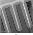
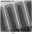
- TEM transmission electron microscopy
- Example 1 PEALD aluminum doped silicon nitride film using trimethylaluminum (TMA), di-iso-propylaminosilane (DIPAS) and nitrogen plasma
- the silicon wafer was loaded into the CN-1 reactor equipped with showerhead design with 13.56 MHz direct plasma and heated to 300°C with chamber pressure of 2 torr.
- the precursors, trimethylaluminum (TMA) as the metal precursor and di-iso-propylaminosilane (DIPAS) as organoaminosilane precursor, were delivered using the vapor draw method into the reactor.
- Nitrogen plasma was used as plasma source.
- silicon nitride helps slightly to improve the growth rate of silicon nitride, i.e., increasing the growth rate from 0.16 ⁇ to 0.19 ⁇ /cycle.
- the step coverage for silicon nitride middle 11% and bottom 32%.
- the silicon wafer was loaded into the CN-1 reactor equipped with showerhead design with 13.56 MHz direct plasma and heated to 300°C with chamber pressure of 2 torr.
- Trimethylaluminum (TMA) was used as metal precursor and nitrogen plasma was used as plasma source.
- TMA Trimethylaluminum
- the ALD cycle was conducted using the following process parameters.
- Steps b to e were repeated for 100 cycles, 200 cycles, and 400 cycles respectively.
- the growth rate for aluminum nitride was calculated from the graph of thickness vs number of cycles as 0.58 ⁇ /cycle.
- Comparable Example 2b PEALD silicon nitride film using di-iso-propylaminosilane (DIPAS) and nitrogen plasma
- the silicon wafer was loaded into the CN-1 reactor equipped with showerhead design with 13.56 MHz direct plasma and heated to 300°C with chamber pressure of 2 torr.
- Di-iso-propylaminosilane (DIPAS) was used as silicon precursor and nitrogen plasma was used as plasma source.
- the growth rate for silicon nitride was calculated from the graph of thickness vs number of cycles as 0.15 ⁇ /cycle.
- Example 2 PEALD aluminum doped silicon nitride film using trimethylaluminum (TMA), di-iso-propylaminosilane (DIPAS), and nitrogen plasma
- the silicon wafer was loaded into the CN-1 reactor equipped with showerhead design with 13.56 MHz direct plasma and heated to 300°C with chamber pressure of 2 torr.
- Trimethylaluminum (TMA) as metal precursor and di-iso-propylaminosilane (DIPAS) as organoaminosilane precursor were delivered using vapor draw method into the reactor.
- the ALD cycle was comprised of the process steps provided in Table 1 and using the following process parameters.
- the super cycle is repeated 50 times (i.e.
- the silicon wafer was loaded into the CN-1 reactor equipped with showerhead design with 13.56 MHz direct plasma and heated to 300°C with chamber pressure of 2 torr.
- Trimethylaluminum (TMA) was used as metal precursor and nitrogen plasma was used as plasma source.
- TMA Trimethylaluminum
- the ALD cycle was conducted using the following process parameters.
- Steps b to e were repeated for 100 cycles, 200 cycles, and 300 cycles respectively.
- the growth rate for aluminum nitride was calculated from the graph of thickness vs number of cycles as 0.72 ⁇ /cycle.
- Example 3 PEALD aluminum doped silicon nitride film using trimethylaluminum (TMA) and di-iso-propylaminosilane (DIPAS), and nitrogen plasma
- the silicon wafer was loaded into the CN-1 reactor equipped with showerhead design with 13.56 MHz direct plasma and heated to 300°C with chamber pressure of 2 torr.
- Trimethylaluminum (TMA) as metal precursor and di-iso-propylaminosilane (DIPAS) as organoaminosilane precursor were delivered using vapor draw method into the reactor.
- Nitrogen plasma was used as plasma.
- one super cycle consisting of aluminum nitride having steps b to e are repeated once, followed by steps f to i for 10 times (i.e.
- the step coverage middle 68% and bottom 82%; this demonstrates that introducing the metal precursor further enhances the step coverage.
- the secondary-ion mass spectrometry (SIMS) measurement of deposited aluminum doped silicon nitride shows Si, 31 at%, Al, 8.5 at%, N, 47 at%, C, 2 at%, 0,1.7 at%, and H,9.5 at%.
- Comparable Example 4a PEALD aluminum nitride film using tris(dimethylamino)aluminum (TDMAA) and nitrogen plasma
- the silicon wafer was loaded into the CN-1 reactor equipped with showerhead design with 13.56 MHz direct plasma and heated to 300°C with chamber pressure of 2 torr. Tris(dimethylamino)aluminum (TDMAA) as metal precursor.
- TDMAA Tris(dimethylamino)aluminum
- Steps b to e were repeated for 100 cycles, 200 cycles, and 300 cycles respectively.
- the growth rate for aluminum nitride was calculated from the graph of thickness vs number of cycles as 0.60 ⁇ /cycle.
- Example 4 PEALD aluminum doped silicon nitride film using tris(dimethylamino)aluminum (TDMAA) and di-iso-propylaminosilane (DIPAS), and nitrogen plasma
- the silicon wafer was loaded into the CN-1 reactor equipped with showerhead design with 13.56 MHz direct plasma and heated to 300°C with chamber pressure of 2 torr.
- Tris(dimethylamino)aluminum (TDMAA) as metal precursor and di-iso-propylaminosilane (DIPAS) as organoaminosilane precursor were delivered using vapor draw method into the reactor.
- Nitrogen plasma was used for plasma.
- one super cycle consisting of aluminum nitride having steps b to e are repeated once, followed by steps f to i for 10 times (i.e.
- Comparable Example 5a PEALD aluminum nitride film using tris(dimethylamino)aluminum (TDMAA) and ammonia plasma
- the silicon wafer was loaded into the CN-1 reactor equipped with showerhead design with 13.56 MHz direct plasma and heated to 300°C with chamber pressure of 2 torr.
- Tris(dimethylamino)aluminum (TDMAA) as metal precursor ammonia plasma was used as plasma source.
- the ALD cycle was conducted using the following process parameters.
- Steps b to e were repeated for 100 cycles, 200 cycles, and 300 cycles respectively.
- the growth rate for aluminum nitride was calculated from the graph of thickness vs number of cycles as 0.74 ⁇ /cycle.
- Comparable Example 5b PEALD silicon nitride film using di-iso-propylaminosilane (DIPAS) and ammonia plasma
- the silicon wafer was loaded into the CN-1 reactor equipped with showerhead design with 13.56 MHz direct plasma and heated to 300°C with chamber pressure of 2 torr.
- di-iso-propylaminosilane (DIPAS) as organoaminosilane precursor and ammonia plasma was used as plasma source.
- the cycle consisting of DIPAS/purge/plasma/purge 1.0s/10s/10*s/15s was repeated for 500 cycles to provide 23 ⁇ corresponding to a silicon nitride growth rate of about 0.046 ⁇ /cycle.
- Example 5 PEALD aluminum doped silicon nitride film using tris(dimethylamino)aluminum (TDMAA), di-iso-propylaminosilane (DIPAS), and ammonia plasma
- the silicon wafer was loaded into the CN-1 reactor equipped with showerhead design with 13.56 MHz direct plasma and heated to 300°C with chamber pressure of 2 torr.
- Tris(dimethylamino)aluminum (TDMAA) as metal precursor and di-iso-propylaminosilane (DIPAS) as organoaminosilane precursor were delivered using vapor draw method into the reactor.
- Ammonia plasma was used for plasma.
- one super cycle consisting of aluminum nitride having steps b to e in Table 1 are repeated once, followed by steps f to i in Table 1 for 10 times (i.e.
- the secondary-ion mass spectrometry (SIMS) measurement of deposited aluminum doped silicon nitride shows Si, 21.2 at%, Al, 2.6 at%, N, 42 at%, C, 0.01 at%, O, 5.5 at%, H, 18.6 at%.
- Comparable Example 6a PEALD silicon nitride film using bis(tert-butylamino)silane (BTBAS) and nitrogen plasma
- the silicon wafer was loaded into the CN-1 reactor equipped with showerhead design with 13.56 MHz direct plasma and heated to 300°C with chamber pressure of 2 torr.
- Bis(tert-butylamino)silane (BTBAS) as organoaminosilane precursor ammonia plasma was used as plasma source.
- the cycle consisting of BTBAS/purge/plasma/purge 1.0s/10s/10*s/10s was repeated for 500, 1000, and 1500 cycles respectively.
- the growth rate for aluminum nitride was calculated from the graph of thickness vs number of cycles as 0.28 ⁇ /cycle.
- Example 6 PEALD aluminum doped silicon nitride film using trimethylaluminum (TMA), bis(tert-butylamino)silane (BTBAS), and nitrogen plasma
- the silicon wafer was loaded into the CN-1 reactor equipped with showerhead design with 13.56 MHz direct plasma and heated to 300°C with chamber pressure of 2 torr.
- Trimethylaluminum (TMA) as metal precursor and bis(tert-butylamino)silane (BTBAS) as organoaminosilane precursor were delivered using vapor draw method into the reactor.
- one super cycle consisting of aluminum nitride having steps b to e in Table 1 were repeated once, followed by steps f to i in Table 1 for 10 times (i.e.
- the secondary-ion mass spectrometry (SIMS) measurement of deposited aluminum doped silicon nitride shows Si, 33.3 at%, Al, 7.1 at%, N, 45.2 at%, C, 2.4 at%, O, 0.7 at%, H,11.3 at%.
- the silicon wafer was loaded into the CN-1 reactor equipped with showerhead design with 13.56 MHz direct plasma and heated to 300°C with chamber pressure of 2 torr.
- Trimethylaluminum (TMA) was used as metal precursor and ammonia plasma was used as plasma source.
- TMA Trimethylaluminum
- the ALD cycle was conducted using the following process parameters.
- Steps b to e were repeated for 200 cycles and 300 cycles respectively.
- the growth rate for aluminum nitride was calculated from the graph of thickness vs number of cycles as 1.21 ⁇ /cycle.
- Comparable Example 7b PEALD silicon nitride film using bis(tert-butylaminosilane (BTBAS) and ammonia plasma
- the silicon wafer was loaded into the CN-1 reactor equipped with showerhead design with 13.56 MHz direct plasma and heated to 300°C with chamber pressure of 2 torr.
- Bis(tert-butylaminosilane (BTBAS) was used as organoaminosilane precursor and ammonia plasma was used as plasma source.
- the cycle consisting of BTBAS/purge/plasma/purge 1.0s/10s/10*s/15s was repeated for 500, 1000, and 1500 cycles.
- the growth rate for silicon nitride was calculated from the graph of thickness vs number of cycles as 0.045 ⁇ /cycle.
- Example 7 PEALD aluminum doped silicon nitride film using trimethylaluminum (TMA), bis(tert-butylamino)silane (BTBAS), and ammonia plasma
- the silicon wafer was loaded into the CN-1 reactor equipped with showerhead design with 13.56 MHz direct plasma and heated to 300°C with chamber pressure of 2 torr.
- Trimethylaluminum (TMA) as metal precursor and bis(tert-butylamino)silane (BTBAS) as organoaminosilane precursor were delivered using vapor draw method into the reactor.
- Ammonia plasma was used as plasma.
- one super cycle consisting of aluminum nitride having steps b to e in Table 1 are repeated once, followed by steps f to i in Table 1 for 10 times (i.e.
- Comparable Example 8a PEALD silicon nitride film using di-iso-propylaminodisilane (DIPADS) and nitrogen plasma
- the silicon wafer was loaded into the CN-1 reactor equipped with showerhead design with 13.56 MHz direct plasma and heated to 300°C with chamber pressure of 2 torr.
- Di-iso-propylaminodisilane (DIPADS) was used as silicon precursor and nitrogen plasma as plasma.
- the growth rate for silicon nitride was calculated from the graph of thickness vs number of cycles as 0.38 ⁇ /cycle.
- the silicon wafer was loaded into the CN-1 reactor equipped with showerhead design with 13.56 MHz direct plasma and heated to 300°C with chamber pressure of 2 torr. Trimethylgallium was used as gallium precursor and nitrogen plasma was used as plasma.
- the growth rate for gallium nitride was calculated from the graph of thickness vs number of cycles as 0.42 ⁇ /cycle.
- Example 8 PEALD gallium doped silicon nitride film using trimethylgallium (TMGa), di-iso-propylaminodisilane (DIPADS), and nitrogen plasma
- TMGa Trimethylgallium
- DIPADS di-iso-propylaminodisilane
- gallium doped silicon nitride 250A corresponding to a silicon nitride growth rate of about 0.48 ⁇ /cycle (about 28% increase compare to PEALD silicon nitride using only DIPADS) assuming 11 ⁇ gallium nitride, demonstrating significant improvement of growth rate of silicon nitride via alternating deposition of gallium nitride and silicon nitride, i.e. deposited gallium nitride layer boosts deposition of silicon nitride.
- one super cycle consisting of gallium nitride having steps b to e in Table 1 are repeated once, followed by steps f to i in Table 1 for 5 times (i.e.
- gallium doped silicon nitride 320A corresponding to a silicon nitride growth rate of about 0.56 ⁇ /cycle (about 47% increase compare to PEALD silicon nitride using only DIPADS) assuming 42 ⁇ gallium nitride, demonstrating significant improvement of growth rate of silicon nitride via alternating deposition of gallium nitride and silicon nitride, i.e. deposited gallium nitride layer boosts deposition of silicon nitride significantly.
- Comparable Example 9a PEALD titanium nitride film using tetrakis(dimethylamino)titanium (TDMAT) and nitrogen plasma
- the silicon wafer was loaded into the CN-1 reactor equipped with showerhead design with 13.56 MHz direct plasma and heated to 300°C with chamber pressure of 2 torr.
- TDMAT was used as titanium precursor and nitrogen plasma was used as plasma source.
- the growth rate for titanium nitride was calculated from the graph of thickness vs number of cycles as 1.11 ⁇ /cycle.
- Example 9 PEALD titanium doped silicon nitride film using tetrakis(dimethylamino)titanium (TDMAT), di-iso-propylaminosilane (DIPAS), and nitrogen plasma
- the silicon wafer was loaded into the CN-1 reactor equipped with showerhead design with 13.56 MHz direct plasma and heated to 300°C with chamber pressure of 2 torr.
- TDMAT tetrakis(dimethylamino)titanium
- DIPAS di-iso-propylaminosilane
- titanium doped silicon nitride 230 ⁇ corresponding to a silicon nitride growth rate of about 0.24 ⁇ /cycle based on XRF measurement of 36 ⁇ of titanium nitride, demonstrating significant improvement of growth rate of silicon nitride via alternating deposition of titanium nitride and silicon nitride, i.e. deposited titanium nitride layer boosts deposition of silicon nitride.
- one super cycle consisting of titanium nitride having steps b to e in Table 1 are repeated 3 times, followed by steps f to i in Table 1 for 20 times (i.e.
- titanium doped silicon nitride 285 ⁇ corresponding to a silicon nitride growth rate of about 0.28 ⁇ /cycle (about 26% increase compare to PEALD silicon nitride using only DIPAS) based on XRF measurement of 65 ⁇ of titanium nitride, demonstrating significant improvement of growth rate of silicon nitride via alternating deposition of titanium nitride and silicon nitride, i.e. deposited titanium nitride layer boosts deposition of silicon nitride significantly.
- Example 10 PEALD titanium doped silicon nitride film using tetrakis(dimethylamino)titanium (TDMAT), bis(tert-butylamino)silane (BTBAS), and nitrogen plasma
- the silicon wafer was loaded into the CN-1 reactor equipped with showerhead design with 13.56 MHz direct plasma and heated to 300°C with chamber pressure of 2 torr.
- Ar flow rate 50sccm
- titanium doped silicon nitride 265 ⁇ corresponding to a silicon nitride growth rate of about 0.29 ⁇ /cycle ( about 26% increase compare to PEALD silicon nitride using only BTBAS) based on XRF measurement of 35 ⁇ of titanium nitride, demonstrating significant improvement of growth rate of silicon nitride via alternating deposition of titanium nitride and silicon nitride, i.e. deposited titanium nitride layer boosts deposition of silicon nitride.
- the super cycle is repeated 40 times (i.e.
- titanium doped silicon nitride 305 ⁇ corresponding to a silicon nitride growth rate of about 0.30 ⁇ /cycle (( about 30% increase compare to PEALD silicon nitride using only BTBAS) based on XRF measurement of 62 ⁇ of titanium nitride, demonstrating significant improvement of growth rate of silicon nitride via alternating deposition of titanium nitride and silicon nitride, i.e. deposited titanium nitride layer boosts deposition of silicon nitride significantly.
Landscapes
- Chemical & Material Sciences (AREA)
- Engineering & Computer Science (AREA)
- Chemical Kinetics & Catalysis (AREA)
- General Chemical & Material Sciences (AREA)
- Materials Engineering (AREA)
- Mechanical Engineering (AREA)
- Metallurgy (AREA)
- Organic Chemistry (AREA)
- Inorganic Chemistry (AREA)
- Physics & Mathematics (AREA)
- Plasma & Fusion (AREA)
- Computer Hardware Design (AREA)
- Condensed Matter Physics & Semiconductors (AREA)
- General Physics & Mathematics (AREA)
- Manufacturing & Machinery (AREA)
- Microelectronics & Electronic Packaging (AREA)
- Power Engineering (AREA)
- Electromagnetism (AREA)
- Chemical Vapour Deposition (AREA)
- Formation Of Insulating Films (AREA)
Applications Claiming Priority (3)
| Application Number | Priority Date | Filing Date | Title |
|---|---|---|---|
| US201562217296P | 2015-09-11 | 2015-09-11 | |
| US201562237899P | 2015-10-06 | 2015-10-06 | |
| PCT/US2016/050874 WO2017044690A1 (en) | 2015-09-11 | 2016-09-09 | Methods for depositing a conformal metal or metalloid silicon nitride film and resultant films |
Publications (2)
| Publication Number | Publication Date |
|---|---|
| EP3347504A1 EP3347504A1 (en) | 2018-07-18 |
| EP3347504B1 true EP3347504B1 (en) | 2024-09-25 |
Family
ID=56940449
Family Applications (1)
| Application Number | Title | Priority Date | Filing Date |
|---|---|---|---|
| EP16766797.1A Active EP3347504B1 (en) | 2015-09-11 | 2016-09-09 | Methods for depositing a conformal metal or metalloid silicon nitride film and resultant films |
Country Status (8)
| Country | Link |
|---|---|
| US (2) | US11104990B2 (OSRAM) |
| EP (1) | EP3347504B1 (OSRAM) |
| JP (1) | JP6761028B2 (OSRAM) |
| KR (2) | KR102251774B1 (OSRAM) |
| CN (2) | CN117265512A (OSRAM) |
| IL (1) | IL257990B2 (OSRAM) |
| TW (1) | TWI642803B (OSRAM) |
| WO (1) | WO2017044690A1 (OSRAM) |
Families Citing this family (330)
| Publication number | Priority date | Publication date | Assignee | Title |
|---|---|---|---|---|
| US9394608B2 (en) | 2009-04-06 | 2016-07-19 | Asm America, Inc. | Semiconductor processing reactor and components thereof |
| US8802201B2 (en) | 2009-08-14 | 2014-08-12 | Asm America, Inc. | Systems and methods for thin-film deposition of metal oxides using excited nitrogen-oxygen species |
| US20130023129A1 (en) | 2011-07-20 | 2013-01-24 | Asm America, Inc. | Pressure transmitter for a semiconductor processing environment |
| US9017481B1 (en) | 2011-10-28 | 2015-04-28 | Asm America, Inc. | Process feed management for semiconductor substrate processing |
| US10714315B2 (en) | 2012-10-12 | 2020-07-14 | Asm Ip Holdings B.V. | Semiconductor reaction chamber showerhead |
| US20160376700A1 (en) | 2013-02-01 | 2016-12-29 | Asm Ip Holding B.V. | System for treatment of deposition reactor |
| US11015245B2 (en) | 2014-03-19 | 2021-05-25 | Asm Ip Holding B.V. | Gas-phase reactor and system having exhaust plenum and components thereof |
| US10858737B2 (en) | 2014-07-28 | 2020-12-08 | Asm Ip Holding B.V. | Showerhead assembly and components thereof |
| US9890456B2 (en) | 2014-08-21 | 2018-02-13 | Asm Ip Holding B.V. | Method and system for in situ formation of gas-phase compounds |
| US10941490B2 (en) | 2014-10-07 | 2021-03-09 | Asm Ip Holding B.V. | Multiple temperature range susceptor, assembly, reactor and system including the susceptor, and methods of using the same |
| US10276355B2 (en) | 2015-03-12 | 2019-04-30 | Asm Ip Holding B.V. | Multi-zone reactor, system including the reactor, and method of using the same |
| US9777025B2 (en) * | 2015-03-30 | 2017-10-03 | L'Air Liquide, Société pour l'Etude et l'Exploitation des Procédés Georges Claude | Si-containing film forming precursors and methods of using the same |
| US10458018B2 (en) | 2015-06-26 | 2019-10-29 | Asm Ip Holding B.V. | Structures including metal carbide material, devices including the structures, and methods of forming same |
| US10745808B2 (en) * | 2015-07-24 | 2020-08-18 | Versum Materials Us, Llc | Methods for depositing Group 13 metal or metalloid nitride films |
| US10211308B2 (en) | 2015-10-21 | 2019-02-19 | Asm Ip Holding B.V. | NbMC layers |
| US11139308B2 (en) | 2015-12-29 | 2021-10-05 | Asm Ip Holding B.V. | Atomic layer deposition of III-V compounds to form V-NAND devices |
| US10529554B2 (en) | 2016-02-19 | 2020-01-07 | Asm Ip Holding B.V. | Method for forming silicon nitride film selectively on sidewalls or flat surfaces of trenches |
| US10343920B2 (en) | 2016-03-18 | 2019-07-09 | Asm Ip Holding B.V. | Aligned carbon nanotubes |
| US10190213B2 (en) | 2016-04-21 | 2019-01-29 | Asm Ip Holding B.V. | Deposition of metal borides |
| US10865475B2 (en) | 2016-04-21 | 2020-12-15 | Asm Ip Holding B.V. | Deposition of metal borides and silicides |
| US10367080B2 (en) | 2016-05-02 | 2019-07-30 | Asm Ip Holding B.V. | Method of forming a germanium oxynitride film |
| US20170323785A1 (en) | 2016-05-06 | 2017-11-09 | Lam Research Corporation | Method to deposit conformal and low wet etch rate encapsulation layer using pecvd |
| US11453943B2 (en) | 2016-05-25 | 2022-09-27 | Asm Ip Holding B.V. | Method for forming carbon-containing silicon/metal oxide or nitride film by ALD using silicon precursor and hydrocarbon precursor |
| US10612137B2 (en) | 2016-07-08 | 2020-04-07 | Asm Ip Holdings B.V. | Organic reactants for atomic layer deposition |
| US9859151B1 (en) | 2016-07-08 | 2018-01-02 | Asm Ip Holding B.V. | Selective film deposition method to form air gaps |
| US10714385B2 (en) | 2016-07-19 | 2020-07-14 | Asm Ip Holding B.V. | Selective deposition of tungsten |
| US9812320B1 (en) | 2016-07-28 | 2017-11-07 | Asm Ip Holding B.V. | Method and apparatus for filling a gap |
| US9887082B1 (en) | 2016-07-28 | 2018-02-06 | Asm Ip Holding B.V. | Method and apparatus for filling a gap |
| KR102532607B1 (ko) | 2016-07-28 | 2023-05-15 | 에이에스엠 아이피 홀딩 비.브이. | 기판 가공 장치 및 그 동작 방법 |
| JP6832785B2 (ja) * | 2016-08-08 | 2021-02-24 | 東京エレクトロン株式会社 | シリコン窒化膜の成膜方法および成膜装置 |
| US10643826B2 (en) | 2016-10-26 | 2020-05-05 | Asm Ip Holdings B.V. | Methods for thermally calibrating reaction chambers |
| US11532757B2 (en) | 2016-10-27 | 2022-12-20 | Asm Ip Holding B.V. | Deposition of charge trapping layers |
| US10229833B2 (en) | 2016-11-01 | 2019-03-12 | Asm Ip Holding B.V. | Methods for forming a transition metal nitride film on a substrate by atomic layer deposition and related semiconductor device structures |
| US10714350B2 (en) | 2016-11-01 | 2020-07-14 | ASM IP Holdings, B.V. | Methods for forming a transition metal niobium nitride film on a substrate by atomic layer deposition and related semiconductor device structures |
| KR102546317B1 (ko) | 2016-11-15 | 2023-06-21 | 에이에스엠 아이피 홀딩 비.브이. | 기체 공급 유닛 및 이를 포함하는 기판 처리 장치 |
| KR102762543B1 (ko) | 2016-12-14 | 2025-02-05 | 에이에스엠 아이피 홀딩 비.브이. | 기판 처리 장치 |
| US11447861B2 (en) | 2016-12-15 | 2022-09-20 | Asm Ip Holding B.V. | Sequential infiltration synthesis apparatus and a method of forming a patterned structure |
| US11581186B2 (en) | 2016-12-15 | 2023-02-14 | Asm Ip Holding B.V. | Sequential infiltration synthesis apparatus |
| KR102700194B1 (ko) | 2016-12-19 | 2024-08-28 | 에이에스엠 아이피 홀딩 비.브이. | 기판 처리 장치 |
| US10269558B2 (en) | 2016-12-22 | 2019-04-23 | Asm Ip Holding B.V. | Method of forming a structure on a substrate |
| US10867788B2 (en) | 2016-12-28 | 2020-12-15 | Asm Ip Holding B.V. | Method of forming a structure on a substrate |
| US11390950B2 (en) | 2017-01-10 | 2022-07-19 | Asm Ip Holding B.V. | Reactor system and method to reduce residue buildup during a film deposition process |
| US10468261B2 (en) | 2017-02-15 | 2019-11-05 | Asm Ip Holding B.V. | Methods for forming a metallic film on a substrate by cyclical deposition and related semiconductor device structures |
| JP6920082B2 (ja) * | 2017-03-17 | 2021-08-18 | 株式会社Kokusai Electric | 半導体装置の製造方法、基板処理装置およびプログラム |
| US10529563B2 (en) | 2017-03-29 | 2020-01-07 | Asm Ip Holdings B.V. | Method for forming doped metal oxide films on a substrate by cyclical deposition and related semiconductor device structures |
| KR102457289B1 (ko) | 2017-04-25 | 2022-10-21 | 에이에스엠 아이피 홀딩 비.브이. | 박막 증착 방법 및 반도체 장치의 제조 방법 |
| US10892156B2 (en) | 2017-05-08 | 2021-01-12 | Asm Ip Holding B.V. | Methods for forming a silicon nitride film on a substrate and related semiconductor device structures |
| US10770286B2 (en) | 2017-05-08 | 2020-09-08 | Asm Ip Holdings B.V. | Methods for selectively forming a silicon nitride film on a substrate and related semiconductor device structures |
| US20180331118A1 (en) * | 2017-05-12 | 2018-11-15 | Sandisk Technologies Llc | Multi-layer barrier for cmos under array type memory device and method of making thereof |
| US10886123B2 (en) | 2017-06-02 | 2021-01-05 | Asm Ip Holding B.V. | Methods for forming low temperature semiconductor layers and related semiconductor device structures |
| US12040200B2 (en) | 2017-06-20 | 2024-07-16 | Asm Ip Holding B.V. | Semiconductor processing apparatus and methods for calibrating a semiconductor processing apparatus |
| US11306395B2 (en) | 2017-06-28 | 2022-04-19 | Asm Ip Holding B.V. | Methods for depositing a transition metal nitride film on a substrate by atomic layer deposition and related deposition apparatus |
| US10685834B2 (en) | 2017-07-05 | 2020-06-16 | Asm Ip Holdings B.V. | Methods for forming a silicon germanium tin layer and related semiconductor device structures |
| KR20190009245A (ko) | 2017-07-18 | 2019-01-28 | 에이에스엠 아이피 홀딩 비.브이. | 반도체 소자 구조물 형성 방법 및 관련된 반도체 소자 구조물 |
| US11374112B2 (en) | 2017-07-19 | 2022-06-28 | Asm Ip Holding B.V. | Method for depositing a group IV semiconductor and related semiconductor device structures |
| US10541333B2 (en) | 2017-07-19 | 2020-01-21 | Asm Ip Holding B.V. | Method for depositing a group IV semiconductor and related semiconductor device structures |
| US11018002B2 (en) | 2017-07-19 | 2021-05-25 | Asm Ip Holding B.V. | Method for selectively depositing a Group IV semiconductor and related semiconductor device structures |
| US10590535B2 (en) | 2017-07-26 | 2020-03-17 | Asm Ip Holdings B.V. | Chemical treatment, deposition and/or infiltration apparatus and method for using the same |
| TWI815813B (zh) | 2017-08-04 | 2023-09-21 | 荷蘭商Asm智慧財產控股公司 | 用於分配反應腔內氣體的噴頭總成 |
| US10692741B2 (en) | 2017-08-08 | 2020-06-23 | Asm Ip Holdings B.V. | Radiation shield |
| US10770336B2 (en) | 2017-08-08 | 2020-09-08 | Asm Ip Holding B.V. | Substrate lift mechanism and reactor including same |
| US11769682B2 (en) | 2017-08-09 | 2023-09-26 | Asm Ip Holding B.V. | Storage apparatus for storing cassettes for substrates and processing apparatus equipped therewith |
| US11139191B2 (en) | 2017-08-09 | 2021-10-05 | Asm Ip Holding B.V. | Storage apparatus for storing cassettes for substrates and processing apparatus equipped therewith |
| US11830730B2 (en) | 2017-08-29 | 2023-11-28 | Asm Ip Holding B.V. | Layer forming method and apparatus |
| US11056344B2 (en) | 2017-08-30 | 2021-07-06 | Asm Ip Holding B.V. | Layer forming method |
| US11295980B2 (en) | 2017-08-30 | 2022-04-05 | Asm Ip Holding B.V. | Methods for depositing a molybdenum metal film over a dielectric surface of a substrate by a cyclical deposition process and related semiconductor device structures |
| KR102491945B1 (ko) | 2017-08-30 | 2023-01-26 | 에이에스엠 아이피 홀딩 비.브이. | 기판 처리 장치 |
| KR102401446B1 (ko) | 2017-08-31 | 2022-05-24 | 에이에스엠 아이피 홀딩 비.브이. | 기판 처리 장치 |
| KR102630301B1 (ko) | 2017-09-21 | 2024-01-29 | 에이에스엠 아이피 홀딩 비.브이. | 침투성 재료의 순차 침투 합성 방법 처리 및 이를 이용하여 형성된 구조물 및 장치 |
| US10844484B2 (en) | 2017-09-22 | 2020-11-24 | Asm Ip Holding B.V. | Apparatus for dispensing a vapor phase reactant to a reaction chamber and related methods |
| US10658205B2 (en) | 2017-09-28 | 2020-05-19 | Asm Ip Holdings B.V. | Chemical dispensing apparatus and methods for dispensing a chemical to a reaction chamber |
| US10403504B2 (en) | 2017-10-05 | 2019-09-03 | Asm Ip Holding B.V. | Method for selectively depositing a metallic film on a substrate |
| US10319588B2 (en) | 2017-10-10 | 2019-06-11 | Asm Ip Holding B.V. | Method for depositing a metal chalcogenide on a substrate by cyclical deposition |
| US10923344B2 (en) | 2017-10-30 | 2021-02-16 | Asm Ip Holding B.V. | Methods for forming a semiconductor structure and related semiconductor structures |
| US10910262B2 (en) | 2017-11-16 | 2021-02-02 | Asm Ip Holding B.V. | Method of selectively depositing a capping layer structure on a semiconductor device structure |
| US11022879B2 (en) | 2017-11-24 | 2021-06-01 | Asm Ip Holding B.V. | Method of forming an enhanced unexposed photoresist layer |
| US11127617B2 (en) | 2017-11-27 | 2021-09-21 | Asm Ip Holding B.V. | Storage device for storing wafer cassettes for use with a batch furnace |
| CN111344522B (zh) | 2017-11-27 | 2022-04-12 | 阿斯莫Ip控股公司 | 包括洁净迷你环境的装置 |
| US10872771B2 (en) | 2018-01-16 | 2020-12-22 | Asm Ip Holding B. V. | Method for depositing a material film on a substrate within a reaction chamber by a cyclical deposition process and related device structures |
| KR102695659B1 (ko) | 2018-01-19 | 2024-08-14 | 에이에스엠 아이피 홀딩 비.브이. | 플라즈마 보조 증착에 의해 갭 충진 층을 증착하는 방법 |
| TWI852426B (zh) | 2018-01-19 | 2024-08-11 | 荷蘭商Asm Ip私人控股有限公司 | 沈積方法 |
| US11018047B2 (en) | 2018-01-25 | 2021-05-25 | Asm Ip Holding B.V. | Hybrid lift pin |
| USD880437S1 (en) | 2018-02-01 | 2020-04-07 | Asm Ip Holding B.V. | Gas supply plate for semiconductor manufacturing apparatus |
| US11081345B2 (en) | 2018-02-06 | 2021-08-03 | Asm Ip Holding B.V. | Method of post-deposition treatment for silicon oxide film |
| EP3737779A1 (en) | 2018-02-14 | 2020-11-18 | ASM IP Holding B.V. | A method for depositing a ruthenium-containing film on a substrate by a cyclical deposition process |
| US10896820B2 (en) | 2018-02-14 | 2021-01-19 | Asm Ip Holding B.V. | Method for depositing a ruthenium-containing film on a substrate by a cyclical deposition process |
| US10731249B2 (en) | 2018-02-15 | 2020-08-04 | Asm Ip Holding B.V. | Method of forming a transition metal containing film on a substrate by a cyclical deposition process, a method for supplying a transition metal halide compound to a reaction chamber, and related vapor deposition apparatus |
| KR102636427B1 (ko) | 2018-02-20 | 2024-02-13 | 에이에스엠 아이피 홀딩 비.브이. | 기판 처리 방법 및 장치 |
| US10975470B2 (en) | 2018-02-23 | 2021-04-13 | Asm Ip Holding B.V. | Apparatus for detecting or monitoring for a chemical precursor in a high temperature environment |
| US11473195B2 (en) | 2018-03-01 | 2022-10-18 | Asm Ip Holding B.V. | Semiconductor processing apparatus and a method for processing a substrate |
| US11629406B2 (en) | 2018-03-09 | 2023-04-18 | Asm Ip Holding B.V. | Semiconductor processing apparatus comprising one or more pyrometers for measuring a temperature of a substrate during transfer of the substrate |
| US11114283B2 (en) | 2018-03-16 | 2021-09-07 | Asm Ip Holding B.V. | Reactor, system including the reactor, and methods of manufacturing and using same |
| KR102646467B1 (ko) | 2018-03-27 | 2024-03-11 | 에이에스엠 아이피 홀딩 비.브이. | 기판 상에 전극을 형성하는 방법 및 전극을 포함하는 반도체 소자 구조 |
| US11088002B2 (en) | 2018-03-29 | 2021-08-10 | Asm Ip Holding B.V. | Substrate rack and a substrate processing system and method |
| US11230766B2 (en) | 2018-03-29 | 2022-01-25 | Asm Ip Holding B.V. | Substrate processing apparatus and method |
| KR102501472B1 (ko) | 2018-03-30 | 2023-02-20 | 에이에스엠 아이피 홀딩 비.브이. | 기판 처리 방법 |
| KR102600229B1 (ko) | 2018-04-09 | 2023-11-10 | 에이에스엠 아이피 홀딩 비.브이. | 기판 지지 장치, 이를 포함하는 기판 처리 장치 및 기판 처리 방법 |
| US12025484B2 (en) | 2018-05-08 | 2024-07-02 | Asm Ip Holding B.V. | Thin film forming method |
| TWI811348B (zh) | 2018-05-08 | 2023-08-11 | 荷蘭商Asm 智慧財產控股公司 | 藉由循環沉積製程於基板上沉積氧化物膜之方法及相關裝置結構 |
| US12272527B2 (en) | 2018-05-09 | 2025-04-08 | Asm Ip Holding B.V. | Apparatus for use with hydrogen radicals and method of using same |
| TWI879056B (zh) | 2018-05-11 | 2025-04-01 | 荷蘭商Asm Ip私人控股有限公司 | 用於基板上形成摻雜金屬碳化物薄膜之方法及相關半導體元件結構 |
| KR102596988B1 (ko) | 2018-05-28 | 2023-10-31 | 에이에스엠 아이피 홀딩 비.브이. | 기판 처리 방법 및 그에 의해 제조된 장치 |
| TWI840362B (zh) | 2018-06-04 | 2024-05-01 | 荷蘭商Asm Ip私人控股有限公司 | 水氣降低的晶圓處置腔室 |
| US11718913B2 (en) | 2018-06-04 | 2023-08-08 | Asm Ip Holding B.V. | Gas distribution system and reactor system including same |
| US11286562B2 (en) | 2018-06-08 | 2022-03-29 | Asm Ip Holding B.V. | Gas-phase chemical reactor and method of using same |
| US10797133B2 (en) | 2018-06-21 | 2020-10-06 | Asm Ip Holding B.V. | Method for depositing a phosphorus doped silicon arsenide film and related semiconductor device structures |
| KR102568797B1 (ko) | 2018-06-21 | 2023-08-21 | 에이에스엠 아이피 홀딩 비.브이. | 기판 처리 시스템 |
| TWI871083B (zh) | 2018-06-27 | 2025-01-21 | 荷蘭商Asm Ip私人控股有限公司 | 用於形成含金屬材料之循環沉積製程 |
| US10879456B2 (en) | 2018-06-27 | 2020-12-29 | Taiwan Semiconductor Manufacturing Co., Ltd. | Sidewall spacer stack for magnetic tunnel junctions |
| JP7515411B2 (ja) | 2018-06-27 | 2024-07-12 | エーエスエム・アイピー・ホールディング・ベー・フェー | 金属含有材料ならびに金属含有材料を含む膜および構造体を形成するための周期的堆積方法 |
| US10612136B2 (en) | 2018-06-29 | 2020-04-07 | ASM IP Holding, B.V. | Temperature-controlled flange and reactor system including same |
| KR102686758B1 (ko) | 2018-06-29 | 2024-07-18 | 에이에스엠 아이피 홀딩 비.브이. | 박막 증착 방법 및 반도체 장치의 제조 방법 |
| US10755922B2 (en) * | 2018-07-03 | 2020-08-25 | Asm Ip Holding B.V. | Method for depositing silicon-free carbon-containing film as gap-fill layer by pulse plasma-assisted deposition |
| US10388513B1 (en) * | 2018-07-03 | 2019-08-20 | Asm Ip Holding B.V. | Method for depositing silicon-free carbon-containing film as gap-fill layer by pulse plasma-assisted deposition |
| US10767789B2 (en) | 2018-07-16 | 2020-09-08 | Asm Ip Holding B.V. | Diaphragm valves, valve components, and methods for forming valve components |
| US11053591B2 (en) | 2018-08-06 | 2021-07-06 | Asm Ip Holding B.V. | Multi-port gas injection system and reactor system including same |
| US10883175B2 (en) | 2018-08-09 | 2021-01-05 | Asm Ip Holding B.V. | Vertical furnace for processing substrates and a liner for use therein |
| US10829852B2 (en) | 2018-08-16 | 2020-11-10 | Asm Ip Holding B.V. | Gas distribution device for a wafer processing apparatus |
| US11430674B2 (en) | 2018-08-22 | 2022-08-30 | Asm Ip Holding B.V. | Sensor array, apparatus for dispensing a vapor phase reactant to a reaction chamber and related methods |
| US11239420B2 (en) | 2018-08-24 | 2022-02-01 | Lam Research Corporation | Conformal damage-free encapsulation of chalcogenide materials |
| KR102707956B1 (ko) | 2018-09-11 | 2024-09-19 | 에이에스엠 아이피 홀딩 비.브이. | 박막 증착 방법 |
| US11024523B2 (en) | 2018-09-11 | 2021-06-01 | Asm Ip Holding B.V. | Substrate processing apparatus and method |
| US11049751B2 (en) | 2018-09-14 | 2021-06-29 | Asm Ip Holding B.V. | Cassette supply system to store and handle cassettes and processing apparatus equipped therewith |
| CN110970344B (zh) | 2018-10-01 | 2024-10-25 | Asmip控股有限公司 | 衬底保持设备、包含所述设备的系统及其使用方法 |
| US11232963B2 (en) | 2018-10-03 | 2022-01-25 | Asm Ip Holding B.V. | Substrate processing apparatus and method |
| KR102592699B1 (ko) | 2018-10-08 | 2023-10-23 | 에이에스엠 아이피 홀딩 비.브이. | 기판 지지 유닛 및 이를 포함하는 박막 증착 장치와 기판 처리 장치 |
| US10847365B2 (en) | 2018-10-11 | 2020-11-24 | Asm Ip Holding B.V. | Method of forming conformal silicon carbide film by cyclic CVD |
| US10811256B2 (en) | 2018-10-16 | 2020-10-20 | Asm Ip Holding B.V. | Method for etching a carbon-containing feature |
| KR102605121B1 (ko) | 2018-10-19 | 2023-11-23 | 에이에스엠 아이피 홀딩 비.브이. | 기판 처리 장치 및 기판 처리 방법 |
| KR102546322B1 (ko) | 2018-10-19 | 2023-06-21 | 에이에스엠 아이피 홀딩 비.브이. | 기판 처리 장치 및 기판 처리 방법 |
| USD948463S1 (en) | 2018-10-24 | 2022-04-12 | Asm Ip Holding B.V. | Susceptor for semiconductor substrate supporting apparatus |
| US12378665B2 (en) | 2018-10-26 | 2025-08-05 | Asm Ip Holding B.V. | High temperature coatings for a preclean and etch apparatus and related methods |
| US11087997B2 (en) | 2018-10-31 | 2021-08-10 | Asm Ip Holding B.V. | Substrate processing apparatus for processing substrates |
| KR102748291B1 (ko) | 2018-11-02 | 2024-12-31 | 에이에스엠 아이피 홀딩 비.브이. | 기판 지지 유닛 및 이를 포함하는 기판 처리 장치 |
| US11572620B2 (en) | 2018-11-06 | 2023-02-07 | Asm Ip Holding B.V. | Methods for selectively depositing an amorphous silicon film on a substrate |
| US11031242B2 (en) | 2018-11-07 | 2021-06-08 | Asm Ip Holding B.V. | Methods for depositing a boron doped silicon germanium film |
| US10847366B2 (en) | 2018-11-16 | 2020-11-24 | Asm Ip Holding B.V. | Methods for depositing a transition metal chalcogenide film on a substrate by a cyclical deposition process |
| US10818758B2 (en) | 2018-11-16 | 2020-10-27 | Asm Ip Holding B.V. | Methods for forming a metal silicate film on a substrate in a reaction chamber and related semiconductor device structures |
| US12040199B2 (en) | 2018-11-28 | 2024-07-16 | Asm Ip Holding B.V. | Substrate processing apparatus for processing substrates |
| US11217444B2 (en) | 2018-11-30 | 2022-01-04 | Asm Ip Holding B.V. | Method for forming an ultraviolet radiation responsive metal oxide-containing film |
| KR102636428B1 (ko) | 2018-12-04 | 2024-02-13 | 에이에스엠 아이피 홀딩 비.브이. | 기판 처리 장치를 세정하는 방법 |
| US20200181770A1 (en) * | 2018-12-05 | 2020-06-11 | Asm Ip Holding B.V. | Method of forming a structure including silicon nitride on titanium nitride and structure formed using the method |
| US11158513B2 (en) | 2018-12-13 | 2021-10-26 | Asm Ip Holding B.V. | Methods for forming a rhenium-containing film on a substrate by a cyclical deposition process and related semiconductor device structures |
| TWI874340B (zh) | 2018-12-14 | 2025-03-01 | 荷蘭商Asm Ip私人控股有限公司 | 形成裝置結構之方法、其所形成之結構及施行其之系統 |
| KR20250026878A (ko) * | 2019-01-02 | 2025-02-25 | 어플라이드 머티어리얼스, 인코포레이티드 | 낮은 누설 전류를 갖는 실리콘 붕소를 포함하는 막들을 형성하기 위한 방법들 |
| TWI866480B (zh) | 2019-01-17 | 2024-12-11 | 荷蘭商Asm Ip 私人控股有限公司 | 藉由循環沈積製程於基板上形成含過渡金屬膜之方法 |
| KR102727227B1 (ko) | 2019-01-22 | 2024-11-07 | 에이에스엠 아이피 홀딩 비.브이. | 기판 처리 장치 |
| CN111524788B (zh) | 2019-02-01 | 2023-11-24 | Asm Ip私人控股有限公司 | 氧化硅的拓扑选择性膜形成的方法 |
| KR102626263B1 (ko) | 2019-02-20 | 2024-01-16 | 에이에스엠 아이피 홀딩 비.브이. | 처리 단계를 포함하는 주기적 증착 방법 및 이를 위한 장치 |
| TWI873122B (zh) | 2019-02-20 | 2025-02-21 | 荷蘭商Asm Ip私人控股有限公司 | 填充一基板之一表面內所形成的一凹槽的方法、根據其所形成之半導體結構、及半導體處理設備 |
| TWI838458B (zh) | 2019-02-20 | 2024-04-11 | 荷蘭商Asm Ip私人控股有限公司 | 用於3d nand應用中之插塞填充沉積之設備及方法 |
| TWI845607B (zh) | 2019-02-20 | 2024-06-21 | 荷蘭商Asm Ip私人控股有限公司 | 用來填充形成於基材表面內之凹部的循環沉積方法及設備 |
| TWI842826B (zh) | 2019-02-22 | 2024-05-21 | 荷蘭商Asm Ip私人控股有限公司 | 基材處理設備及處理基材之方法 |
| KR102782593B1 (ko) | 2019-03-08 | 2025-03-14 | 에이에스엠 아이피 홀딩 비.브이. | SiOC 층을 포함한 구조체 및 이의 형성 방법 |
| US11742198B2 (en) | 2019-03-08 | 2023-08-29 | Asm Ip Holding B.V. | Structure including SiOCN layer and method of forming same |
| KR102858005B1 (ko) | 2019-03-08 | 2025-09-09 | 에이에스엠 아이피 홀딩 비.브이. | 실리콘 질화물 층을 선택적으로 증착하는 방법, 및 선택적으로 증착된 실리콘 질화물 층을 포함하는 구조체 |
| KR20200116033A (ko) | 2019-03-28 | 2020-10-08 | 에이에스엠 아이피 홀딩 비.브이. | 도어 개방기 및 이를 구비한 기판 처리 장치 |
| KR102809999B1 (ko) | 2019-04-01 | 2025-05-19 | 에이에스엠 아이피 홀딩 비.브이. | 반도체 소자를 제조하는 방법 |
| US11447864B2 (en) | 2019-04-19 | 2022-09-20 | Asm Ip Holding B.V. | Layer forming method and apparatus |
| KR20200125453A (ko) | 2019-04-24 | 2020-11-04 | 에이에스엠 아이피 홀딩 비.브이. | 기상 반응기 시스템 및 이를 사용하는 방법 |
| KR102869364B1 (ko) | 2019-05-07 | 2025-10-10 | 에이에스엠 아이피 홀딩 비.브이. | 비정질 탄소 중합체 막을 개질하는 방법 |
| KR20200130121A (ko) | 2019-05-07 | 2020-11-18 | 에이에스엠 아이피 홀딩 비.브이. | 딥 튜브가 있는 화학물질 공급원 용기 |
| KR20200130652A (ko) | 2019-05-10 | 2020-11-19 | 에이에스엠 아이피 홀딩 비.브이. | 표면 상에 재료를 증착하는 방법 및 본 방법에 따라 형성된 구조 |
| JP7598201B2 (ja) | 2019-05-16 | 2024-12-11 | エーエスエム・アイピー・ホールディング・ベー・フェー | ウェハボートハンドリング装置、縦型バッチ炉および方法 |
| JP7612342B2 (ja) | 2019-05-16 | 2025-01-14 | エーエスエム・アイピー・ホールディング・ベー・フェー | ウェハボートハンドリング装置、縦型バッチ炉および方法 |
| USD975665S1 (en) | 2019-05-17 | 2023-01-17 | Asm Ip Holding B.V. | Susceptor shaft |
| USD947913S1 (en) | 2019-05-17 | 2022-04-05 | Asm Ip Holding B.V. | Susceptor shaft |
| USD935572S1 (en) | 2019-05-24 | 2021-11-09 | Asm Ip Holding B.V. | Gas channel plate |
| US20200381623A1 (en) * | 2019-05-31 | 2020-12-03 | Applied Materials, Inc. | Methods of forming silicon nitride encapsulation layers |
| USD922229S1 (en) | 2019-06-05 | 2021-06-15 | Asm Ip Holding B.V. | Device for controlling a temperature of a gas supply unit |
| KR20200141002A (ko) | 2019-06-06 | 2020-12-17 | 에이에스엠 아이피 홀딩 비.브이. | 배기 가스 분석을 포함한 기상 반응기 시스템을 사용하는 방법 |
| KR20200141931A (ko) | 2019-06-10 | 2020-12-21 | 에이에스엠 아이피 홀딩 비.브이. | 석영 에피택셜 챔버를 세정하는 방법 |
| KR20200143254A (ko) | 2019-06-11 | 2020-12-23 | 에이에스엠 아이피 홀딩 비.브이. | 개질 가스를 사용하여 전자 구조를 형성하는 방법, 상기 방법을 수행하기 위한 시스템, 및 상기 방법을 사용하여 형성되는 구조 |
| USD944946S1 (en) | 2019-06-14 | 2022-03-01 | Asm Ip Holding B.V. | Shower plate |
| USD931978S1 (en) | 2019-06-27 | 2021-09-28 | Asm Ip Holding B.V. | Showerhead vacuum transport |
| KR20210005515A (ko) | 2019-07-03 | 2021-01-14 | 에이에스엠 아이피 홀딩 비.브이. | 기판 처리 장치용 온도 제어 조립체 및 이를 사용하는 방법 |
| JP7499079B2 (ja) | 2019-07-09 | 2024-06-13 | エーエスエム・アイピー・ホールディング・ベー・フェー | 同軸導波管を用いたプラズマ装置、基板処理方法 |
| CN112216646A (zh) | 2019-07-10 | 2021-01-12 | Asm Ip私人控股有限公司 | 基板支撑组件及包括其的基板处理装置 |
| KR102895115B1 (ko) | 2019-07-16 | 2025-12-03 | 에이에스엠 아이피 홀딩 비.브이. | 기판 처리 장치 |
| KR20210010816A (ko) | 2019-07-17 | 2021-01-28 | 에이에스엠 아이피 홀딩 비.브이. | 라디칼 보조 점화 플라즈마 시스템 및 방법 |
| KR102860110B1 (ko) | 2019-07-17 | 2025-09-16 | 에이에스엠 아이피 홀딩 비.브이. | 실리콘 게르마늄 구조를 형성하는 방법 |
| US11643724B2 (en) | 2019-07-18 | 2023-05-09 | Asm Ip Holding B.V. | Method of forming structures using a neutral beam |
| CN112242295B (zh) | 2019-07-19 | 2025-12-09 | Asmip私人控股有限公司 | 形成拓扑受控的无定形碳聚合物膜的方法 |
| TWI839544B (zh) | 2019-07-19 | 2024-04-21 | 荷蘭商Asm Ip私人控股有限公司 | 形成形貌受控的非晶碳聚合物膜之方法 |
| CN112309843A (zh) | 2019-07-29 | 2021-02-02 | Asm Ip私人控股有限公司 | 实现高掺杂剂掺入的选择性沉积方法 |
| CN112309900B (zh) | 2019-07-30 | 2025-11-04 | Asmip私人控股有限公司 | 基板处理设备 |
| CN112309899B (zh) | 2019-07-30 | 2025-11-14 | Asmip私人控股有限公司 | 基板处理设备 |
| KR20210015655A (ko) | 2019-07-30 | 2021-02-10 | 에이에스엠 아이피 홀딩 비.브이. | 기판 처리 장치 및 방법 |
| US11587815B2 (en) | 2019-07-31 | 2023-02-21 | Asm Ip Holding B.V. | Vertical batch furnace assembly |
| US11587814B2 (en) | 2019-07-31 | 2023-02-21 | Asm Ip Holding B.V. | Vertical batch furnace assembly |
| US11227782B2 (en) | 2019-07-31 | 2022-01-18 | Asm Ip Holding B.V. | Vertical batch furnace assembly |
| KR20210018759A (ko) | 2019-08-05 | 2021-02-18 | 에이에스엠 아이피 홀딩 비.브이. | 화학물질 공급원 용기를 위한 액체 레벨 센서 |
| KR20210018761A (ko) | 2019-08-09 | 2021-02-18 | 에이에스엠 아이피 홀딩 비.브이. | 냉각 장치를 포함한 히터 어셈블리 및 이를 사용하는 방법 |
| JP7246284B2 (ja) * | 2019-08-15 | 2023-03-27 | 東京エレクトロン株式会社 | 成膜方法 |
| USD965524S1 (en) | 2019-08-19 | 2022-10-04 | Asm Ip Holding B.V. | Susceptor support |
| USD965044S1 (en) | 2019-08-19 | 2022-09-27 | Asm Ip Holding B.V. | Susceptor shaft |
| JP2021031769A (ja) | 2019-08-21 | 2021-03-01 | エーエスエム アイピー ホールディング ビー.ブイ. | 成膜原料混合ガス生成装置及び成膜装置 |
| USD949319S1 (en) | 2019-08-22 | 2022-04-19 | Asm Ip Holding B.V. | Exhaust duct |
| KR20210024423A (ko) | 2019-08-22 | 2021-03-05 | 에이에스엠 아이피 홀딩 비.브이. | 홀을 구비한 구조체를 형성하기 위한 방법 |
| USD930782S1 (en) | 2019-08-22 | 2021-09-14 | Asm Ip Holding B.V. | Gas distributor |
| USD940837S1 (en) | 2019-08-22 | 2022-01-11 | Asm Ip Holding B.V. | Electrode |
| USD979506S1 (en) | 2019-08-22 | 2023-02-28 | Asm Ip Holding B.V. | Insulator |
| KR20210024420A (ko) | 2019-08-23 | 2021-03-05 | 에이에스엠 아이피 홀딩 비.브이. | 비스(디에틸아미노)실란을 사용하여 peald에 의해 개선된 품질을 갖는 실리콘 산화물 막을 증착하기 위한 방법 |
| US11286558B2 (en) | 2019-08-23 | 2022-03-29 | Asm Ip Holding B.V. | Methods for depositing a molybdenum nitride film on a surface of a substrate by a cyclical deposition process and related semiconductor device structures including a molybdenum nitride film |
| KR102806450B1 (ko) | 2019-09-04 | 2025-05-12 | 에이에스엠 아이피 홀딩 비.브이. | 희생 캡핑 층을 이용한 선택적 증착 방법 |
| KR102733104B1 (ko) | 2019-09-05 | 2024-11-22 | 에이에스엠 아이피 홀딩 비.브이. | 기판 처리 장치 |
| JP2022548037A (ja) * | 2019-09-11 | 2022-11-16 | バーサム マテリアルズ ユーエス,リミティド ライアビリティ カンパニー | ケイ素ドープ酸化ハフニウムの堆積のための配合物 |
| US12469693B2 (en) | 2019-09-17 | 2025-11-11 | Asm Ip Holding B.V. | Method of forming a carbon-containing layer and structure including the layer |
| KR102156663B1 (ko) * | 2019-09-25 | 2020-09-21 | 솔브레인 주식회사 | 박막 제조 방법 |
| US11562901B2 (en) | 2019-09-25 | 2023-01-24 | Asm Ip Holding B.V. | Substrate processing method |
| CN112593212B (zh) | 2019-10-02 | 2023-12-22 | Asm Ip私人控股有限公司 | 通过循环等离子体增强沉积工艺形成拓扑选择性氧化硅膜的方法 |
| KR20210042810A (ko) | 2019-10-08 | 2021-04-20 | 에이에스엠 아이피 홀딩 비.브이. | 활성 종을 이용하기 위한 가스 분배 어셈블리를 포함한 반응기 시스템 및 이를 사용하는 방법 |
| TWI846953B (zh) | 2019-10-08 | 2024-07-01 | 荷蘭商Asm Ip私人控股有限公司 | 基板處理裝置 |
| TW202128273A (zh) | 2019-10-08 | 2021-08-01 | 荷蘭商Asm Ip私人控股有限公司 | 氣體注入系統、及將材料沉積於反應室內之基板表面上的方法 |
| KR102879443B1 (ko) | 2019-10-10 | 2025-11-03 | 에이에스엠 아이피 홀딩 비.브이. | 포토레지스트 하부층을 형성하기 위한 방법 및 이를 포함한 구조체 |
| US12009241B2 (en) | 2019-10-14 | 2024-06-11 | Asm Ip Holding B.V. | Vertical batch furnace assembly with detector to detect cassette |
| TWI834919B (zh) | 2019-10-16 | 2024-03-11 | 荷蘭商Asm Ip私人控股有限公司 | 氧化矽之拓撲選擇性膜形成之方法 |
| US11637014B2 (en) | 2019-10-17 | 2023-04-25 | Asm Ip Holding B.V. | Methods for selective deposition of doped semiconductor material |
| KR102845724B1 (ko) | 2019-10-21 | 2025-08-13 | 에이에스엠 아이피 홀딩 비.브이. | 막을 선택적으로 에칭하기 위한 장치 및 방법 |
| KR20210050453A (ko) | 2019-10-25 | 2021-05-07 | 에이에스엠 아이피 홀딩 비.브이. | 기판 표면 상의 갭 피처를 충진하는 방법 및 이와 관련된 반도체 소자 구조 |
| US11646205B2 (en) | 2019-10-29 | 2023-05-09 | Asm Ip Holding B.V. | Methods of selectively forming n-type doped material on a surface, systems for selectively forming n-type doped material, and structures formed using same |
| KR102890638B1 (ko) | 2019-11-05 | 2025-11-25 | 에이에스엠 아이피 홀딩 비.브이. | 도핑된 반도체 층을 갖는 구조체 및 이를 형성하기 위한 방법 및 시스템 |
| US11501968B2 (en) | 2019-11-15 | 2022-11-15 | Asm Ip Holding B.V. | Method for providing a semiconductor device with silicon filled gaps |
| KR102861314B1 (ko) | 2019-11-20 | 2025-09-17 | 에이에스엠 아이피 홀딩 비.브이. | 기판의 표면 상에 탄소 함유 물질을 증착하는 방법, 상기 방법을 사용하여 형성된 구조물, 및 상기 구조물을 형성하기 위한 시스템 |
| US11450529B2 (en) | 2019-11-26 | 2022-09-20 | Asm Ip Holding B.V. | Methods for selectively forming a target film on a substrate comprising a first dielectric surface and a second metallic surface |
| CN112951697B (zh) | 2019-11-26 | 2025-07-29 | Asmip私人控股有限公司 | 基板处理设备 |
| CN112885693B (zh) | 2019-11-29 | 2025-06-10 | Asmip私人控股有限公司 | 基板处理设备 |
| CN112885692B (zh) | 2019-11-29 | 2025-08-15 | Asmip私人控股有限公司 | 基板处理设备 |
| JP7527928B2 (ja) | 2019-12-02 | 2024-08-05 | エーエスエム・アイピー・ホールディング・ベー・フェー | 基板処理装置、基板処理方法 |
| KR20210070898A (ko) | 2019-12-04 | 2021-06-15 | 에이에스엠 아이피 홀딩 비.브이. | 기판 처리 장치 |
| JP7703317B2 (ja) | 2019-12-17 | 2025-07-07 | エーエスエム・アイピー・ホールディング・ベー・フェー | 窒化バナジウム層および窒化バナジウム層を含む構造体を形成する方法 |
| US11482414B2 (en) * | 2019-12-18 | 2022-10-25 | L'Air Liquide, Société Anonyme pour l'Etude et l'Exploitation des Procédés Georges Claude | Ultra-low temperature ALD to form high-quality Si-containing film |
| KR20210080214A (ko) | 2019-12-19 | 2021-06-30 | 에이에스엠 아이피 홀딩 비.브이. | 기판 상의 갭 피처를 충진하는 방법 및 이와 관련된 반도체 소자 구조 |
| KR102818620B1 (ko) * | 2019-12-20 | 2025-06-10 | 삼성전자주식회사 | 물질막 형성 방법과, 집적회로 소자 및 그 제조 방법 |
| CN111162088B (zh) * | 2020-01-02 | 2023-01-24 | 长江存储科技有限责任公司 | 含硅衬底中凹槽的制作方法、三维nand存储器及制作方法 |
| TWI887322B (zh) | 2020-01-06 | 2025-06-21 | 荷蘭商Asm Ip私人控股有限公司 | 反應器系統、抬升銷、及處理方法 |
| JP7730637B2 (ja) | 2020-01-06 | 2025-08-28 | エーエスエム・アイピー・ホールディング・ベー・フェー | ガス供給アセンブリ、その構成要素、およびこれを含む反応器システム |
| US11993847B2 (en) | 2020-01-08 | 2024-05-28 | Asm Ip Holding B.V. | Injector |
| KR102882467B1 (ko) | 2020-01-16 | 2025-11-05 | 에이에스엠 아이피 홀딩 비.브이. | 고 종횡비 피처를 형성하는 방법 |
| KR102675856B1 (ko) | 2020-01-20 | 2024-06-17 | 에이에스엠 아이피 홀딩 비.브이. | 박막 형성 방법 및 박막 표면 개질 방법 |
| TWI889744B (zh) | 2020-01-29 | 2025-07-11 | 荷蘭商Asm Ip私人控股有限公司 | 污染物捕集系統、及擋板堆疊 |
| TWI871421B (zh) | 2020-02-03 | 2025-02-01 | 荷蘭商Asm Ip私人控股有限公司 | 包括釩或銦層的裝置、結構及其形成方法、系統 |
| KR20210100010A (ko) | 2020-02-04 | 2021-08-13 | 에이에스엠 아이피 홀딩 비.브이. | 대형 물품의 투과율 측정을 위한 방법 및 장치 |
| US11776846B2 (en) | 2020-02-07 | 2023-10-03 | Asm Ip Holding B.V. | Methods for depositing gap filling fluids and related systems and devices |
| TW202146691A (zh) | 2020-02-13 | 2021-12-16 | 荷蘭商Asm Ip私人控股有限公司 | 氣體分配總成、噴淋板總成、及調整至反應室之氣體的傳導率之方法 |
| KR20210103956A (ko) | 2020-02-13 | 2021-08-24 | 에이에스엠 아이피 홀딩 비.브이. | 수광 장치를 포함하는 기판 처리 장치 및 수광 장치의 교정 방법 |
| US11781243B2 (en) | 2020-02-17 | 2023-10-10 | Asm Ip Holding B.V. | Method for depositing low temperature phosphorous-doped silicon |
| TWI895326B (zh) | 2020-02-28 | 2025-09-01 | 荷蘭商Asm Ip私人控股有限公司 | 專用於零件清潔的系統 |
| KR20210113043A (ko) | 2020-03-04 | 2021-09-15 | 에이에스엠 아이피 홀딩 비.브이. | 반응기 시스템용 정렬 고정구 |
| KR20210116249A (ko) | 2020-03-11 | 2021-09-27 | 에이에스엠 아이피 홀딩 비.브이. | 록아웃 태그아웃 어셈블리 및 시스템 그리고 이의 사용 방법 |
| KR20210116240A (ko) | 2020-03-11 | 2021-09-27 | 에이에스엠 아이피 홀딩 비.브이. | 조절성 접합부를 갖는 기판 핸들링 장치 |
| KR102775390B1 (ko) | 2020-03-12 | 2025-02-28 | 에이에스엠 아이피 홀딩 비.브이. | 타겟 토폴로지 프로파일을 갖는 층 구조를 제조하기 위한 방법 |
| US12173404B2 (en) | 2020-03-17 | 2024-12-24 | Asm Ip Holding B.V. | Method of depositing epitaxial material, structure formed using the method, and system for performing the method |
| US12071688B2 (en) | 2020-03-31 | 2024-08-27 | Entegris, Inc. | Precursors and methods for preparing silicon-containing films |
| EP4130335A4 (en) | 2020-04-01 | 2024-07-03 | Adeka Corporation | Material for formation of thin film for use in atomic layer deposition and method for producing thin film |
| KR102755229B1 (ko) | 2020-04-02 | 2025-01-14 | 에이에스엠 아이피 홀딩 비.브이. | 박막 형성 방법 |
| TWI887376B (zh) | 2020-04-03 | 2025-06-21 | 荷蘭商Asm Ip私人控股有限公司 | 半導體裝置的製造方法 |
| TWI888525B (zh) | 2020-04-08 | 2025-07-01 | 荷蘭商Asm Ip私人控股有限公司 | 用於選擇性蝕刻氧化矽膜之設備及方法 |
| KR20210128343A (ko) | 2020-04-15 | 2021-10-26 | 에이에스엠 아이피 홀딩 비.브이. | 크롬 나이트라이드 층을 형성하는 방법 및 크롬 나이트라이드 층을 포함하는 구조 |
| US11821078B2 (en) | 2020-04-15 | 2023-11-21 | Asm Ip Holding B.V. | Method for forming precoat film and method for forming silicon-containing film |
| US11996289B2 (en) | 2020-04-16 | 2024-05-28 | Asm Ip Holding B.V. | Methods of forming structures including silicon germanium and silicon layers, devices formed using the methods, and systems for performing the methods |
| TW202143328A (zh) | 2020-04-21 | 2021-11-16 | 荷蘭商Asm Ip私人控股有限公司 | 用於調整膜應力之方法 |
| KR20210132612A (ko) | 2020-04-24 | 2021-11-04 | 에이에스엠 아이피 홀딩 비.브이. | 바나듐 화합물들을 안정화하기 위한 방법들 및 장치 |
| CN113555279A (zh) | 2020-04-24 | 2021-10-26 | Asm Ip私人控股有限公司 | 形成含氮化钒的层的方法及包含其的结构 |
| KR102866804B1 (ko) | 2020-04-24 | 2025-09-30 | 에이에스엠 아이피 홀딩 비.브이. | 냉각 가스 공급부를 포함한 수직형 배치 퍼니스 어셈블리 |
| TW202208671A (zh) | 2020-04-24 | 2022-03-01 | 荷蘭商Asm Ip私人控股有限公司 | 形成包括硼化釩及磷化釩層的結構之方法 |
| KR20210132600A (ko) | 2020-04-24 | 2021-11-04 | 에이에스엠 아이피 홀딩 비.브이. | 바나듐, 질소 및 추가 원소를 포함한 층을 증착하기 위한 방법 및 시스템 |
| KR102783898B1 (ko) | 2020-04-29 | 2025-03-18 | 에이에스엠 아이피 홀딩 비.브이. | 고체 소스 전구체 용기 |
| KR20210134869A (ko) | 2020-05-01 | 2021-11-11 | 에이에스엠 아이피 홀딩 비.브이. | Foup 핸들러를 이용한 foup의 빠른 교환 |
| JP7726664B2 (ja) | 2020-05-04 | 2025-08-20 | エーエスエム・アイピー・ホールディング・ベー・フェー | 基板を処理するための基板処理システム |
| JP7736446B2 (ja) | 2020-05-07 | 2025-09-09 | エーエスエム・アイピー・ホールディング・ベー・フェー | 同調回路を備える反応器システム |
| KR102788543B1 (ko) | 2020-05-13 | 2025-03-27 | 에이에스엠 아이피 홀딩 비.브이. | 반응기 시스템용 레이저 정렬 고정구 |
| TW202146699A (zh) | 2020-05-15 | 2021-12-16 | 荷蘭商Asm Ip私人控股有限公司 | 形成矽鍺層之方法、半導體結構、半導體裝置、形成沉積層之方法、及沉積系統 |
| TW202147383A (zh) | 2020-05-19 | 2021-12-16 | 荷蘭商Asm Ip私人控股有限公司 | 基材處理設備 |
| KR102795476B1 (ko) | 2020-05-21 | 2025-04-11 | 에이에스엠 아이피 홀딩 비.브이. | 다수의 탄소 층을 포함한 구조체 및 이를 형성하고 사용하는 방법 |
| KR20210145079A (ko) | 2020-05-21 | 2021-12-01 | 에이에스엠 아이피 홀딩 비.브이. | 기판을 처리하기 위한 플랜지 및 장치 |
| KR102702526B1 (ko) | 2020-05-22 | 2024-09-03 | 에이에스엠 아이피 홀딩 비.브이. | 과산화수소를 사용하여 박막을 증착하기 위한 장치 |
| JP7683912B2 (ja) * | 2020-05-26 | 2025-05-27 | 株式会社高純度化学研究所 | 結晶性の窒化ガリウム薄膜の製造方法 |
| TW202212650A (zh) | 2020-05-26 | 2022-04-01 | 荷蘭商Asm Ip私人控股有限公司 | 沉積含硼及鎵的矽鍺層之方法 |
| WO2021241281A1 (ja) * | 2020-05-26 | 2021-12-02 | 株式会社高純度化学研究所 | 結晶性の窒化ガリウム薄膜の製造方法 |
| TWI876048B (zh) | 2020-05-29 | 2025-03-11 | 荷蘭商Asm Ip私人控股有限公司 | 基板處理方法 |
| TW202212620A (zh) | 2020-06-02 | 2022-04-01 | 荷蘭商Asm Ip私人控股有限公司 | 處理基板之設備、形成膜之方法、及控制用於處理基板之設備之方法 |
| TW202208659A (zh) | 2020-06-16 | 2022-03-01 | 荷蘭商Asm Ip私人控股有限公司 | 沉積含硼之矽鍺層的方法 |
| KR20210158809A (ko) | 2020-06-24 | 2021-12-31 | 에이에스엠 아이피 홀딩 비.브이. | 실리콘이 구비된 층을 형성하는 방법 |
| TWI873359B (zh) | 2020-06-30 | 2025-02-21 | 荷蘭商Asm Ip私人控股有限公司 | 基板處理方法 |
| TWI896694B (zh) | 2020-07-01 | 2025-09-11 | 荷蘭商Asm Ip私人控股有限公司 | 沉積方法、半導體結構、及沉積系統 |
| KR102707957B1 (ko) | 2020-07-08 | 2024-09-19 | 에이에스엠 아이피 홀딩 비.브이. | 기판 처리 방법 |
| KR20220010438A (ko) | 2020-07-17 | 2022-01-25 | 에이에스엠 아이피 홀딩 비.브이. | 포토리소그래피에 사용하기 위한 구조체 및 방법 |
| KR20220011092A (ko) | 2020-07-20 | 2022-01-27 | 에이에스엠 아이피 홀딩 비.브이. | 전이 금속층을 포함하는 구조체를 형성하기 위한 방법 및 시스템 |
| TWI878570B (zh) | 2020-07-20 | 2025-04-01 | 荷蘭商Asm Ip私人控股有限公司 | 用於沉積鉬層之方法及系統 |
| US12322591B2 (en) | 2020-07-27 | 2025-06-03 | Asm Ip Holding B.V. | Thin film deposition process |
| KR20220021863A (ko) | 2020-08-14 | 2022-02-22 | 에이에스엠 아이피 홀딩 비.브이. | 기판 처리 방법 |
| US12040177B2 (en) | 2020-08-18 | 2024-07-16 | Asm Ip Holding B.V. | Methods for forming a laminate film by cyclical plasma-enhanced deposition processes |
| TW202228863A (zh) | 2020-08-25 | 2022-08-01 | 荷蘭商Asm Ip私人控股有限公司 | 清潔基板的方法、選擇性沉積的方法、及反應器系統 |
| US11725280B2 (en) | 2020-08-26 | 2023-08-15 | Asm Ip Holding B.V. | Method for forming metal silicon oxide and metal silicon oxynitride layers |
| TW202229601A (zh) | 2020-08-27 | 2022-08-01 | 荷蘭商Asm Ip私人控股有限公司 | 形成圖案化結構的方法、操控機械特性的方法、裝置結構、及基板處理系統 |
| KR20220033997A (ko) | 2020-09-10 | 2022-03-17 | 에이에스엠 아이피 홀딩 비.브이. | 갭 충진 유체를 증착하기 위한 방법 그리고 이와 관련된 시스템 및 장치 |
| USD990534S1 (en) | 2020-09-11 | 2023-06-27 | Asm Ip Holding B.V. | Weighted lift pin |
| KR20220036866A (ko) | 2020-09-16 | 2022-03-23 | 에이에스엠 아이피 홀딩 비.브이. | 실리콘 산화물 증착 방법 |
| USD1012873S1 (en) | 2020-09-24 | 2024-01-30 | Asm Ip Holding B.V. | Electrode for semiconductor processing apparatus |
| TWI889903B (zh) | 2020-09-25 | 2025-07-11 | 荷蘭商Asm Ip私人控股有限公司 | 基板處理方法 |
| US12009224B2 (en) | 2020-09-29 | 2024-06-11 | Asm Ip Holding B.V. | Apparatus and method for etching metal nitrides |
| KR20220045900A (ko) | 2020-10-06 | 2022-04-13 | 에이에스엠 아이피 홀딩 비.브이. | 실리콘 함유 재료를 증착하기 위한 증착 방법 및 장치 |
| CN114293174A (zh) | 2020-10-07 | 2022-04-08 | Asm Ip私人控股有限公司 | 气体供应单元和包括气体供应单元的衬底处理设备 |
| TW202229613A (zh) | 2020-10-14 | 2022-08-01 | 荷蘭商Asm Ip私人控股有限公司 | 於階梯式結構上沉積材料的方法 |
| KR102873665B1 (ko) | 2020-10-15 | 2025-10-17 | 에이에스엠 아이피 홀딩 비.브이. | 반도체 소자의 제조 방법, 및 ether-cat을 사용하는 기판 처리 장치 |
| TW202217037A (zh) | 2020-10-22 | 2022-05-01 | 荷蘭商Asm Ip私人控股有限公司 | 沉積釩金屬的方法、結構、裝置及沉積總成 |
| KR20230088488A (ko) * | 2020-10-23 | 2023-06-19 | 엔테그리스, 아이엔씨. | 아이오도실란의 제조 방법 |
| TW202223136A (zh) | 2020-10-28 | 2022-06-16 | 荷蘭商Asm Ip私人控股有限公司 | 用於在基板上形成層之方法、及半導體處理系統 |
| TW202229620A (zh) | 2020-11-12 | 2022-08-01 | 特文特大學 | 沉積系統、用於控制反應條件之方法、沉積方法 |
| TW202229795A (zh) | 2020-11-23 | 2022-08-01 | 荷蘭商Asm Ip私人控股有限公司 | 具注入器之基板處理設備 |
| TW202235649A (zh) | 2020-11-24 | 2022-09-16 | 荷蘭商Asm Ip私人控股有限公司 | 填充間隙之方法與相關之系統及裝置 |
| KR20220076343A (ko) | 2020-11-30 | 2022-06-08 | 에이에스엠 아이피 홀딩 비.브이. | 기판 처리 장치의 반응 챔버 내에 배열되도록 구성된 인젝터 |
| US12255053B2 (en) | 2020-12-10 | 2025-03-18 | Asm Ip Holding B.V. | Methods and systems for depositing a layer |
| TW202233884A (zh) | 2020-12-14 | 2022-09-01 | 荷蘭商Asm Ip私人控股有限公司 | 形成臨限電壓控制用之結構的方法 |
| US11946137B2 (en) | 2020-12-16 | 2024-04-02 | Asm Ip Holding B.V. | Runout and wobble measurement fixtures |
| TW202232639A (zh) | 2020-12-18 | 2022-08-16 | 荷蘭商Asm Ip私人控股有限公司 | 具有可旋轉台的晶圓處理設備 |
| TW202242184A (zh) | 2020-12-22 | 2022-11-01 | 荷蘭商Asm Ip私人控股有限公司 | 前驅物膠囊、前驅物容器、氣相沉積總成、及將固態前驅物裝載至前驅物容器中之方法 |
| TW202231903A (zh) | 2020-12-22 | 2022-08-16 | 荷蘭商Asm Ip私人控股有限公司 | 過渡金屬沉積方法、過渡金屬層、用於沉積過渡金屬於基板上的沉積總成 |
| TW202226899A (zh) | 2020-12-22 | 2022-07-01 | 荷蘭商Asm Ip私人控股有限公司 | 具匹配器的電漿處理裝置 |
| USD981973S1 (en) | 2021-05-11 | 2023-03-28 | Asm Ip Holding B.V. | Reactor wall for substrate processing apparatus |
| USD980813S1 (en) | 2021-05-11 | 2023-03-14 | Asm Ip Holding B.V. | Gas flow control plate for substrate processing apparatus |
| USD1023959S1 (en) | 2021-05-11 | 2024-04-23 | Asm Ip Holding B.V. | Electrode for substrate processing apparatus |
| USD980814S1 (en) | 2021-05-11 | 2023-03-14 | Asm Ip Holding B.V. | Gas distributor for substrate processing apparatus |
| USD990441S1 (en) | 2021-09-07 | 2023-06-27 | Asm Ip Holding B.V. | Gas flow control plate |
| USD1099184S1 (en) | 2021-11-29 | 2025-10-21 | Asm Ip Holding B.V. | Weighted lift pin |
| USD1060598S1 (en) | 2021-12-03 | 2025-02-04 | Asm Ip Holding B.V. | Split showerhead cover |
| WO2024129836A1 (en) * | 2022-12-16 | 2024-06-20 | Villanova University | Biscationic quaternary phosphonium compounds as soft antimicrobial agents |
| KR20250172051A (ko) * | 2024-05-31 | 2025-12-09 | 주식회사 유피케미칼 | 실리콘-함유 막의 형성 방법 및 이를 위한 조성물 |
| CN120741106B (zh) * | 2025-09-03 | 2025-11-11 | 胜科纳米(苏州)股份有限公司 | 一种表面非平整材料的dsims样品制备方法 |
Family Cites Families (22)
| Publication number | Priority date | Publication date | Assignee | Title |
|---|---|---|---|---|
| US3974003A (en) | 1975-08-25 | 1976-08-10 | Ibm | Chemical vapor deposition of dielectric films containing Al, N, and Si |
| US7081271B2 (en) * | 2001-12-07 | 2006-07-25 | Applied Materials, Inc. | Cyclical deposition of refractory metal silicon nitride |
| US20050287747A1 (en) * | 2004-06-29 | 2005-12-29 | International Business Machines Corporation | Doped nitride film, doped oxide film and other doped films |
| US20060182885A1 (en) * | 2005-02-14 | 2006-08-17 | Xinjian Lei | Preparation of metal silicon nitride films via cyclic deposition |
| US7678422B2 (en) * | 2006-12-13 | 2010-03-16 | Air Products And Chemicals, Inc. | Cyclic chemical vapor deposition of metal-silicon containing films |
| KR100956210B1 (ko) | 2007-06-19 | 2010-05-04 | 에어 프로덕츠 앤드 케미칼스, 인코오포레이티드 | 금속 실리콘 질화물 박막의 플라즈마 강화 사이클릭증착방법 |
| JP2009260151A (ja) * | 2008-04-18 | 2009-11-05 | Tokyo Electron Ltd | 金属ドープ層の形成方法、成膜装置及び記憶媒体 |
| JP5384291B2 (ja) | 2008-11-26 | 2014-01-08 | 株式会社日立国際電気 | 半導体装置の製造方法、基板処理方法及び基板処理装置 |
| WO2010151856A2 (en) | 2009-06-26 | 2010-12-29 | Cornell University | Chemical vapor deposition process for aluminum silicon nitride |
| TWI498447B (zh) | 2010-04-01 | 2015-09-01 | Air Liquide | 使用胺基金屬與鹵化金屬前驅物組合之含金屬氮化物之薄膜沈積 |
| US8912353B2 (en) * | 2010-06-02 | 2014-12-16 | Air Products And Chemicals, Inc. | Organoaminosilane precursors and methods for depositing films comprising same |
| KR101295031B1 (ko) | 2011-04-22 | 2013-08-09 | 에어 프로덕츠 앤드 케미칼스, 인코오포레이티드 | 금속 실리콘 질화물 박막의 플라즈마 강화 사이클릭 증착방법 |
| US8771807B2 (en) * | 2011-05-24 | 2014-07-08 | Air Products And Chemicals, Inc. | Organoaminosilane precursors and methods for making and using same |
| US8993072B2 (en) * | 2011-09-27 | 2015-03-31 | Air Products And Chemicals, Inc. | Halogenated organoaminosilane precursors and methods for depositing films comprising same |
| TWI563539B (en) | 2012-01-18 | 2016-12-21 | Sino American Silicon Prod Inc | Composite substrate, manufacturing method thereof and light emitting device having the same |
| US8912101B2 (en) * | 2012-03-15 | 2014-12-16 | Asm Ip Holding B.V. | Method for forming Si-containing film using two precursors by ALD |
| US9460912B2 (en) * | 2012-04-12 | 2016-10-04 | Air Products And Chemicals, Inc. | High temperature atomic layer deposition of silicon oxide thin films |
| US9337018B2 (en) * | 2012-06-01 | 2016-05-10 | Air Products And Chemicals, Inc. | Methods for depositing films with organoaminodisilane precursors |
| US20140273516A1 (en) * | 2013-03-13 | 2014-09-18 | Applied Materials, Inc. | Vbd and tddb improvement thru interface engineering |
| TWI649803B (zh) * | 2013-09-30 | 2019-02-01 | 蘭姆研究公司 | 具有電漿輔助式原子層沉積及電漿輔助式化學氣相沉積合成法之深寬比可變的特徵物之間隙填充 |
| US9905415B2 (en) * | 2013-10-03 | 2018-02-27 | Versum Materials Us, Llc | Methods for depositing silicon nitride films |
| WO2015103358A1 (en) | 2014-01-05 | 2015-07-09 | Applied Materials, Inc. | Film deposition using spatial atomic layer deposition or pulsed chemical vapor deposition |
-
2016
- 2016-09-09 CN CN202311209900.2A patent/CN117265512A/zh active Pending
- 2016-09-09 CN CN201680052609.0A patent/CN108026637A/zh active Pending
- 2016-09-09 WO PCT/US2016/050874 patent/WO2017044690A1/en not_active Ceased
- 2016-09-09 KR KR1020207034629A patent/KR102251774B1/ko active Active
- 2016-09-09 JP JP2018512922A patent/JP6761028B2/ja active Active
- 2016-09-09 EP EP16766797.1A patent/EP3347504B1/en active Active
- 2016-09-09 KR KR1020187010145A patent/KR102188750B1/ko active Active
- 2016-09-09 US US15/757,805 patent/US11104990B2/en active Active
- 2016-09-09 TW TW105129400A patent/TWI642803B/zh active
-
2018
- 2018-03-08 IL IL257990A patent/IL257990B2/en unknown
-
2021
- 2021-08-26 US US17/458,183 patent/US11732351B2/en active Active
Also Published As
| Publication number | Publication date |
|---|---|
| JP2018528615A (ja) | 2018-09-27 |
| US11732351B2 (en) | 2023-08-22 |
| JP6761028B2 (ja) | 2020-09-23 |
| WO2017044690A1 (en) | 2017-03-16 |
| KR20200137053A (ko) | 2020-12-08 |
| IL257990B1 (en) | 2023-03-01 |
| TWI642803B (zh) | 2018-12-01 |
| US20180245215A1 (en) | 2018-08-30 |
| TW201710538A (zh) | 2017-03-16 |
| IL257990A (en) | 2018-05-31 |
| US11104990B2 (en) | 2021-08-31 |
| KR102188750B1 (ko) | 2020-12-08 |
| CN108026637A (zh) | 2018-05-11 |
| EP3347504A1 (en) | 2018-07-18 |
| KR102251774B1 (ko) | 2021-05-12 |
| US20210388489A1 (en) | 2021-12-16 |
| IL257990B2 (en) | 2023-07-01 |
| KR20180053694A (ko) | 2018-05-23 |
| CN117265512A (zh) | 2023-12-22 |
Similar Documents
| Publication | Publication Date | Title |
|---|---|---|
| US11732351B2 (en) | Methods for depositing a conformal metal or metalloid silicon nitride film and resultant films | |
| JP6437962B2 (ja) | 13族金属又は半金属の窒化物膜の堆積方法 | |
| US11605535B2 (en) | Boron-containing compounds, compositions, and methods for the deposition of a boron containing films | |
| US12163224B2 (en) | Methods for depositing a conformal metal or metalloid silicon nitride film | |
| JP2017533589A (ja) | ケイ素含有膜の堆積のための組成物及びそれを使用した方法 |
Legal Events
| Date | Code | Title | Description |
|---|---|---|---|
| STAA | Information on the status of an ep patent application or granted ep patent |
Free format text: STATUS: THE INTERNATIONAL PUBLICATION HAS BEEN MADE |
|
| PUAI | Public reference made under article 153(3) epc to a published international application that has entered the european phase |
Free format text: ORIGINAL CODE: 0009012 |
|
| STAA | Information on the status of an ep patent application or granted ep patent |
Free format text: STATUS: REQUEST FOR EXAMINATION WAS MADE |
|
| 17P | Request for examination filed |
Effective date: 20180405 |
|
| AK | Designated contracting states |
Kind code of ref document: A1 Designated state(s): AL AT BE BG CH CY CZ DE DK EE ES FI FR GB GR HR HU IE IS IT LI LT LU LV MC MK MT NL NO PL PT RO RS SE SI SK SM TR |
|
| AX | Request for extension of the european patent |
Extension state: BA ME |
|
| RAP1 | Party data changed (applicant data changed or rights of an application transferred) |
Owner name: VERSUM MATERIALS US, LLC |
|
| DAV | Request for validation of the european patent (deleted) | ||
| DAX | Request for extension of the european patent (deleted) | ||
| STAA | Information on the status of an ep patent application or granted ep patent |
Free format text: STATUS: EXAMINATION IS IN PROGRESS |
|
| 17Q | First examination report despatched |
Effective date: 20210929 |
|
| P01 | Opt-out of the competence of the unified patent court (upc) registered |
Effective date: 20230602 |
|
| GRAP | Despatch of communication of intention to grant a patent |
Free format text: ORIGINAL CODE: EPIDOSNIGR1 |
|
| STAA | Information on the status of an ep patent application or granted ep patent |
Free format text: STATUS: GRANT OF PATENT IS INTENDED |
|
| INTG | Intention to grant announced |
Effective date: 20231019 |
|
| GRAJ | Information related to disapproval of communication of intention to grant by the applicant or resumption of examination proceedings by the epo deleted |
Free format text: ORIGINAL CODE: EPIDOSDIGR1 |
|
| STAA | Information on the status of an ep patent application or granted ep patent |
Free format text: STATUS: EXAMINATION IS IN PROGRESS |
|
| INTC | Intention to grant announced (deleted) | ||
| GRAP | Despatch of communication of intention to grant a patent |
Free format text: ORIGINAL CODE: EPIDOSNIGR1 |
|
| STAA | Information on the status of an ep patent application or granted ep patent |
Free format text: STATUS: GRANT OF PATENT IS INTENDED |
|
| INTG | Intention to grant announced |
Effective date: 20240415 |
|
| GRAS | Grant fee paid |
Free format text: ORIGINAL CODE: EPIDOSNIGR3 |
|
| GRAA | (expected) grant |
Free format text: ORIGINAL CODE: 0009210 |
|
| STAA | Information on the status of an ep patent application or granted ep patent |
Free format text: STATUS: THE PATENT HAS BEEN GRANTED |
|
| AK | Designated contracting states |
Kind code of ref document: B1 Designated state(s): AL AT BE BG CH CY CZ DE DK EE ES FI FR GB GR HR HU IE IS IT LI LT LU LV MC MK MT NL NO PL PT RO RS SE SI SK SM TR |
|
| REG | Reference to a national code |
Ref country code: GB Ref legal event code: FG4D |
|
| REG | Reference to a national code |
Ref country code: CH Ref legal event code: EP |
|
| REG | Reference to a national code |
Ref country code: DE Ref legal event code: R096 Ref document number: 602016089563 Country of ref document: DE |
|
| REG | Reference to a national code |
Ref country code: IE Ref legal event code: FG4D |
|
| REG | Reference to a national code |
Ref country code: LT Ref legal event code: MG9D |
|
| PG25 | Lapsed in a contracting state [announced via postgrant information from national office to epo] |
Ref country code: NO Free format text: LAPSE BECAUSE OF FAILURE TO SUBMIT A TRANSLATION OF THE DESCRIPTION OR TO PAY THE FEE WITHIN THE PRESCRIBED TIME-LIMIT Effective date: 20241225 |
|
| PG25 | Lapsed in a contracting state [announced via postgrant information from national office to epo] |
Ref country code: GR Free format text: LAPSE BECAUSE OF FAILURE TO SUBMIT A TRANSLATION OF THE DESCRIPTION OR TO PAY THE FEE WITHIN THE PRESCRIBED TIME-LIMIT Effective date: 20241226 Ref country code: FI Free format text: LAPSE BECAUSE OF FAILURE TO SUBMIT A TRANSLATION OF THE DESCRIPTION OR TO PAY THE FEE WITHIN THE PRESCRIBED TIME-LIMIT Effective date: 20240925 |
|
| PG25 | Lapsed in a contracting state [announced via postgrant information from national office to epo] |
Ref country code: BG Free format text: LAPSE BECAUSE OF FAILURE TO SUBMIT A TRANSLATION OF THE DESCRIPTION OR TO PAY THE FEE WITHIN THE PRESCRIBED TIME-LIMIT Effective date: 20240925 |
|
| PG25 | Lapsed in a contracting state [announced via postgrant information from national office to epo] |
Ref country code: LV Free format text: LAPSE BECAUSE OF FAILURE TO SUBMIT A TRANSLATION OF THE DESCRIPTION OR TO PAY THE FEE WITHIN THE PRESCRIBED TIME-LIMIT Effective date: 20240925 |
|
| PG25 | Lapsed in a contracting state [announced via postgrant information from national office to epo] |
Ref country code: RS Free format text: LAPSE BECAUSE OF FAILURE TO SUBMIT A TRANSLATION OF THE DESCRIPTION OR TO PAY THE FEE WITHIN THE PRESCRIBED TIME-LIMIT Effective date: 20241225 |
|
| REG | Reference to a national code |
Ref country code: NL Ref legal event code: MP Effective date: 20240925 |
|
| PG25 | Lapsed in a contracting state [announced via postgrant information from national office to epo] |
Ref country code: RS Free format text: LAPSE BECAUSE OF FAILURE TO SUBMIT A TRANSLATION OF THE DESCRIPTION OR TO PAY THE FEE WITHIN THE PRESCRIBED TIME-LIMIT Effective date: 20241225 Ref country code: NO Free format text: LAPSE BECAUSE OF FAILURE TO SUBMIT A TRANSLATION OF THE DESCRIPTION OR TO PAY THE FEE WITHIN THE PRESCRIBED TIME-LIMIT Effective date: 20241225 Ref country code: LV Free format text: LAPSE BECAUSE OF FAILURE TO SUBMIT A TRANSLATION OF THE DESCRIPTION OR TO PAY THE FEE WITHIN THE PRESCRIBED TIME-LIMIT Effective date: 20240925 Ref country code: GR Free format text: LAPSE BECAUSE OF FAILURE TO SUBMIT A TRANSLATION OF THE DESCRIPTION OR TO PAY THE FEE WITHIN THE PRESCRIBED TIME-LIMIT Effective date: 20241226 Ref country code: FI Free format text: LAPSE BECAUSE OF FAILURE TO SUBMIT A TRANSLATION OF THE DESCRIPTION OR TO PAY THE FEE WITHIN THE PRESCRIBED TIME-LIMIT Effective date: 20240925 Ref country code: BG Free format text: LAPSE BECAUSE OF FAILURE TO SUBMIT A TRANSLATION OF THE DESCRIPTION OR TO PAY THE FEE WITHIN THE PRESCRIBED TIME-LIMIT Effective date: 20240925 |
|
| REG | Reference to a national code |
Ref country code: AT Ref legal event code: MK05 Ref document number: 1726691 Country of ref document: AT Kind code of ref document: T Effective date: 20240925 |
|
| PG25 | Lapsed in a contracting state [announced via postgrant information from national office to epo] |
Ref country code: NL Free format text: LAPSE BECAUSE OF FAILURE TO SUBMIT A TRANSLATION OF THE DESCRIPTION OR TO PAY THE FEE WITHIN THE PRESCRIBED TIME-LIMIT Effective date: 20240925 |
|
| PG25 | Lapsed in a contracting state [announced via postgrant information from national office to epo] |
Ref country code: PT Free format text: LAPSE BECAUSE OF FAILURE TO SUBMIT A TRANSLATION OF THE DESCRIPTION OR TO PAY THE FEE WITHIN THE PRESCRIBED TIME-LIMIT Effective date: 20250127 Ref country code: IS Free format text: LAPSE BECAUSE OF FAILURE TO SUBMIT A TRANSLATION OF THE DESCRIPTION OR TO PAY THE FEE WITHIN THE PRESCRIBED TIME-LIMIT Effective date: 20250125 |
|
| PG25 | Lapsed in a contracting state [announced via postgrant information from national office to epo] |
Ref country code: RO Free format text: LAPSE BECAUSE OF FAILURE TO SUBMIT A TRANSLATION OF THE DESCRIPTION OR TO PAY THE FEE WITHIN THE PRESCRIBED TIME-LIMIT Effective date: 20240925 Ref country code: SM Free format text: LAPSE BECAUSE OF FAILURE TO SUBMIT A TRANSLATION OF THE DESCRIPTION OR TO PAY THE FEE WITHIN THE PRESCRIBED TIME-LIMIT Effective date: 20240925 |
|
| PG25 | Lapsed in a contracting state [announced via postgrant information from national office to epo] |
Ref country code: ES Free format text: LAPSE BECAUSE OF FAILURE TO SUBMIT A TRANSLATION OF THE DESCRIPTION OR TO PAY THE FEE WITHIN THE PRESCRIBED TIME-LIMIT Effective date: 20240925 |
|
| PG25 | Lapsed in a contracting state [announced via postgrant information from national office to epo] |
Ref country code: EE Free format text: LAPSE BECAUSE OF FAILURE TO SUBMIT A TRANSLATION OF THE DESCRIPTION OR TO PAY THE FEE WITHIN THE PRESCRIBED TIME-LIMIT Effective date: 20240925 Ref country code: AT Free format text: LAPSE BECAUSE OF FAILURE TO SUBMIT A TRANSLATION OF THE DESCRIPTION OR TO PAY THE FEE WITHIN THE PRESCRIBED TIME-LIMIT Effective date: 20240925 |
|
| PG25 | Lapsed in a contracting state [announced via postgrant information from national office to epo] |
Ref country code: CZ Free format text: LAPSE BECAUSE OF FAILURE TO SUBMIT A TRANSLATION OF THE DESCRIPTION OR TO PAY THE FEE WITHIN THE PRESCRIBED TIME-LIMIT Effective date: 20240925 Ref country code: PL Free format text: LAPSE BECAUSE OF FAILURE TO SUBMIT A TRANSLATION OF THE DESCRIPTION OR TO PAY THE FEE WITHIN THE PRESCRIBED TIME-LIMIT Effective date: 20240925 |
|
| PG25 | Lapsed in a contracting state [announced via postgrant information from national office to epo] |
Ref country code: IT Free format text: LAPSE BECAUSE OF FAILURE TO SUBMIT A TRANSLATION OF THE DESCRIPTION OR TO PAY THE FEE WITHIN THE PRESCRIBED TIME-LIMIT Effective date: 20240925 Ref country code: SK Free format text: LAPSE BECAUSE OF FAILURE TO SUBMIT A TRANSLATION OF THE DESCRIPTION OR TO PAY THE FEE WITHIN THE PRESCRIBED TIME-LIMIT Effective date: 20240925 |
|
| REG | Reference to a national code |
Ref country code: DE Ref legal event code: R097 Ref document number: 602016089563 Country of ref document: DE |
|
| PG25 | Lapsed in a contracting state [announced via postgrant information from national office to epo] |
Ref country code: DK Free format text: LAPSE BECAUSE OF FAILURE TO SUBMIT A TRANSLATION OF THE DESCRIPTION OR TO PAY THE FEE WITHIN THE PRESCRIBED TIME-LIMIT Effective date: 20240925 |
|
| PLBE | No opposition filed within time limit |
Free format text: ORIGINAL CODE: 0009261 |
|
| STAA | Information on the status of an ep patent application or granted ep patent |
Free format text: STATUS: NO OPPOSITION FILED WITHIN TIME LIMIT |
|
| 26N | No opposition filed |
Effective date: 20250626 |
|
| PG25 | Lapsed in a contracting state [announced via postgrant information from national office to epo] |
Ref country code: SE Free format text: LAPSE BECAUSE OF FAILURE TO SUBMIT A TRANSLATION OF THE DESCRIPTION OR TO PAY THE FEE WITHIN THE PRESCRIBED TIME-LIMIT Effective date: 20240925 |
|
| PGFP | Annual fee paid to national office [announced via postgrant information from national office to epo] |
Ref country code: DE Payment date: 20250820 Year of fee payment: 10 |
|
| PGFP | Annual fee paid to national office [announced via postgrant information from national office to epo] |
Ref country code: FR Payment date: 20250820 Year of fee payment: 10 |
|
| PGFP | Annual fee paid to national office [announced via postgrant information from national office to epo] |
Ref country code: IE Payment date: 20250822 Year of fee payment: 10 |