EP2784635A1 - Berührungsempfindliche vorrichtung und verfahren zu ihrer herstellung - Google Patents
Berührungsempfindliche vorrichtung und verfahren zu ihrer herstellung Download PDFInfo
- Publication number
- EP2784635A1 EP2784635A1 EP12852049.1A EP12852049A EP2784635A1 EP 2784635 A1 EP2784635 A1 EP 2784635A1 EP 12852049 A EP12852049 A EP 12852049A EP 2784635 A1 EP2784635 A1 EP 2784635A1
- Authority
- EP
- European Patent Office
- Prior art keywords
- bonding
- mark
- bonding mark
- sensing device
- circuit board
- Prior art date
- Legal status (The legal status is an assumption and is not a legal conclusion. Google has not performed a legal analysis and makes no representation as to the accuracy of the status listed.)
- Withdrawn
Links
Images


Classifications
-
- H—ELECTRICITY
- H01—ELECTRIC ELEMENTS
- H01H—ELECTRIC SWITCHES; RELAYS; SELECTORS; EMERGENCY PROTECTIVE DEVICES
- H01H65/00—Apparatus or processes specially adapted to the manufacture of selector switches or parts thereof
-
- G—PHYSICS
- G06—COMPUTING OR CALCULATING; COUNTING
- G06F—ELECTRIC DIGITAL DATA PROCESSING
- G06F3/00—Input arrangements for transferring data to be processed into a form capable of being handled by the computer; Output arrangements for transferring data from processing unit to output unit, e.g. interface arrangements
- G06F3/01—Input arrangements or combined input and output arrangements for interaction between user and computer
- G06F3/03—Arrangements for converting the position or the displacement of a member into a coded form
- G06F3/041—Digitisers, e.g. for touch screens or touch pads, characterised by the transducing means
- G06F3/0416—Control or interface arrangements specially adapted for digitisers
- G06F3/04164—Connections between sensors and controllers, e.g. routing lines between electrodes and connection pads
-
- G—PHYSICS
- G06—COMPUTING OR CALCULATING; COUNTING
- G06F—ELECTRIC DIGITAL DATA PROCESSING
- G06F3/00—Input arrangements for transferring data to be processed into a form capable of being handled by the computer; Output arrangements for transferring data from processing unit to output unit, e.g. interface arrangements
- G06F3/01—Input arrangements or combined input and output arrangements for interaction between user and computer
- G06F3/03—Arrangements for converting the position or the displacement of a member into a coded form
- G06F3/041—Digitisers, e.g. for touch screens or touch pads, characterised by the transducing means
-
- H—ELECTRICITY
- H05—ELECTRIC TECHNIQUES NOT OTHERWISE PROVIDED FOR
- H05K—PRINTED CIRCUITS; CASINGS OR CONSTRUCTIONAL DETAILS OF ELECTRIC APPARATUS; MANUFACTURE OF ASSEMBLAGES OF ELECTRICAL COMPONENTS
- H05K1/00—Printed circuits
- H05K1/02—Details
- H05K1/0266—Marks, test patterns or identification means
- H05K1/0269—Marks, test patterns or identification means for visual or optical inspection
-
- G—PHYSICS
- G06—COMPUTING OR CALCULATING; COUNTING
- G06F—ELECTRIC DIGITAL DATA PROCESSING
- G06F2203/00—Indexing scheme relating to G06F3/00 - G06F3/048
- G06F2203/041—Indexing scheme relating to G06F3/041 - G06F3/045
- G06F2203/04103—Manufacturing, i.e. details related to manufacturing processes specially suited for touch sensitive devices
-
- G—PHYSICS
- G06—COMPUTING OR CALCULATING; COUNTING
- G06F—ELECTRIC DIGITAL DATA PROCESSING
- G06F3/00—Input arrangements for transferring data to be processed into a form capable of being handled by the computer; Output arrangements for transferring data from processing unit to output unit, e.g. interface arrangements
- G06F3/01—Input arrangements or combined input and output arrangements for interaction between user and computer
- G06F3/02—Input arrangements using manually operated switches, e.g. using keyboards or dials
- G06F3/0202—Constructional details or processes of manufacture of the input device
-
- H—ELECTRICITY
- H01—ELECTRIC ELEMENTS
- H01R—ELECTRICALLY-CONDUCTIVE CONNECTIONS; STRUCTURAL ASSOCIATIONS OF A PLURALITY OF MUTUALLY-INSULATED ELECTRICAL CONNECTING ELEMENTS; COUPLING DEVICES; CURRENT COLLECTORS
- H01R12/00—Structural associations of a plurality of mutually-insulated electrical connecting elements, specially adapted for printed circuits, e.g. printed circuit boards [PCB], flat or ribbon cables, or like generally planar structures, e.g. terminal strips, terminal blocks; Coupling devices specially adapted for printed circuits, flat or ribbon cables, or like generally planar structures; Terminals specially adapted for contact with, or insertion into, printed circuits, flat or ribbon cables, or like generally planar structures
- H01R12/50—Fixed connections
- H01R12/59—Fixed connections for flexible printed circuits, flat or ribbon cables or like structures
- H01R12/62—Fixed connections for flexible printed circuits, flat or ribbon cables or like structures connecting to rigid printed circuits or like structures
-
- H—ELECTRICITY
- H05—ELECTRIC TECHNIQUES NOT OTHERWISE PROVIDED FOR
- H05K—PRINTED CIRCUITS; CASINGS OR CONSTRUCTIONAL DETAILS OF ELECTRIC APPARATUS; MANUFACTURE OF ASSEMBLAGES OF ELECTRICAL COMPONENTS
- H05K2201/00—Indexing scheme relating to printed circuits covered by H05K1/00
- H05K2201/09—Shape and layout
- H05K2201/09818—Shape or layout details not covered by a single group of H05K2201/09009 - H05K2201/09809
- H05K2201/09918—Optically detected marks used for aligning tool relative to the PCB, e.g. for mounting of components
-
- H—ELECTRICITY
- H05—ELECTRIC TECHNIQUES NOT OTHERWISE PROVIDED FOR
- H05K—PRINTED CIRCUITS; CASINGS OR CONSTRUCTIONAL DETAILS OF ELECTRIC APPARATUS; MANUFACTURE OF ASSEMBLAGES OF ELECTRICAL COMPONENTS
- H05K2201/00—Indexing scheme relating to printed circuits covered by H05K1/00
- H05K2201/10—Details of components or other objects attached to or integrated in a printed circuit board
- H05K2201/10007—Types of components
- H05K2201/10053—Switch
-
- H—ELECTRICITY
- H05—ELECTRIC TECHNIQUES NOT OTHERWISE PROVIDED FOR
- H05K—PRINTED CIRCUITS; CASINGS OR CONSTRUCTIONAL DETAILS OF ELECTRIC APPARATUS; MANUFACTURE OF ASSEMBLAGES OF ELECTRICAL COMPONENTS
- H05K2201/00—Indexing scheme relating to printed circuits covered by H05K1/00
- H05K2201/10—Details of components or other objects attached to or integrated in a printed circuit board
- H05K2201/10007—Types of components
- H05K2201/10128—Display
-
- H—ELECTRICITY
- H05—ELECTRIC TECHNIQUES NOT OTHERWISE PROVIDED FOR
- H05K—PRINTED CIRCUITS; CASINGS OR CONSTRUCTIONAL DETAILS OF ELECTRIC APPARATUS; MANUFACTURE OF ASSEMBLAGES OF ELECTRICAL COMPONENTS
- H05K2203/00—Indexing scheme relating to apparatus or processes for manufacturing printed circuits covered by H05K3/00
- H05K2203/16—Inspection; Monitoring; Aligning
- H05K2203/166—Alignment or registration; Control of registration
-
- H—ELECTRICITY
- H05—ELECTRIC TECHNIQUES NOT OTHERWISE PROVIDED FOR
- H05K—PRINTED CIRCUITS; CASINGS OR CONSTRUCTIONAL DETAILS OF ELECTRIC APPARATUS; MANUFACTURE OF ASSEMBLAGES OF ELECTRICAL COMPONENTS
- H05K3/00—Apparatus or processes for manufacturing printed circuits
- H05K3/0008—Apparatus or processes for manufacturing printed circuits for aligning or positioning of tools relative to the circuit board
-
- H—ELECTRICITY
- H05—ELECTRIC TECHNIQUES NOT OTHERWISE PROVIDED FOR
- H05K—PRINTED CIRCUITS; CASINGS OR CONSTRUCTIONAL DETAILS OF ELECTRIC APPARATUS; MANUFACTURE OF ASSEMBLAGES OF ELECTRICAL COMPONENTS
- H05K3/00—Apparatus or processes for manufacturing printed circuits
- H05K3/30—Assembling printed circuits with electric components, e.g. with resistors
- H05K3/32—Assembling printed circuits with electric components, e.g. with resistors electrically connecting electric components or wires to printed circuits
- H05K3/321—Assembling printed circuits with electric components, e.g. with resistors electrically connecting electric components or wires to printed circuits by conductive adhesives
- H05K3/323—Assembling printed circuits with electric components, e.g. with resistors electrically connecting electric components or wires to printed circuits by conductive adhesives by applying an anisotropic conductive adhesive layer over an array of pads
-
- H—ELECTRICITY
- H05—ELECTRIC TECHNIQUES NOT OTHERWISE PROVIDED FOR
- H05K—PRINTED CIRCUITS; CASINGS OR CONSTRUCTIONAL DETAILS OF ELECTRIC APPARATUS; MANUFACTURE OF ASSEMBLAGES OF ELECTRICAL COMPONENTS
- H05K3/00—Apparatus or processes for manufacturing printed circuits
- H05K3/36—Assembling printed circuits with other printed circuits
- H05K3/361—Assembling flexible printed circuits with other printed circuits
-
- H—ELECTRICITY
- H05—ELECTRIC TECHNIQUES NOT OTHERWISE PROVIDED FOR
- H05K—PRINTED CIRCUITS; CASINGS OR CONSTRUCTIONAL DETAILS OF ELECTRIC APPARATUS; MANUFACTURE OF ASSEMBLAGES OF ELECTRICAL COMPONENTS
- H05K3/00—Apparatus or processes for manufacturing printed circuits
- H05K3/46—Manufacturing multilayer circuits
- H05K3/4611—Manufacturing multilayer circuits by laminating two or more circuit boards
- H05K3/4638—Aligning and fixing the circuit boards before lamination; Detecting or measuring the misalignment after lamination; Aligning external circuit patterns or via connections relative to internal circuits
-
- H—ELECTRICITY
- H10—SEMICONDUCTOR DEVICES; ELECTRIC SOLID-STATE DEVICES NOT OTHERWISE PROVIDED FOR
- H10W—GENERIC PACKAGES, INTERCONNECTIONS, CONNECTORS OR OTHER CONSTRUCTIONAL DETAILS OF DEVICES COVERED BY CLASS H10
- H10W46/00—Marks applied to devices, e.g. for alignment or identification
-
- Y—GENERAL TAGGING OF NEW TECHNOLOGICAL DEVELOPMENTS; GENERAL TAGGING OF CROSS-SECTIONAL TECHNOLOGIES SPANNING OVER SEVERAL SECTIONS OF THE IPC; TECHNICAL SUBJECTS COVERED BY FORMER USPC CROSS-REFERENCE ART COLLECTIONS [XRACs] AND DIGESTS
- Y10—TECHNICAL SUBJECTS COVERED BY FORMER USPC
- Y10T—TECHNICAL SUBJECTS COVERED BY FORMER US CLASSIFICATION
- Y10T29/00—Metal working
- Y10T29/49—Method of mechanical manufacture
- Y10T29/49002—Electrical device making
- Y10T29/49105—Switch making
Definitions
- the present disclosure relates to a touch sensing device. More particularly, the present disclosure relates to a touch sensing device having a bonding mark for contraposition.
- the process of bonding a touch panel with a flexible printing circuit generally utilizes a charge coupled device (CCD) to get a bonding mark disposed on the touch panel and flexible printing circuit board for positioning.
- CCD charge coupled device
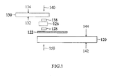
- FIG 1 is a schematic diagram of bonding a traditional touch sensing device, which is drawn with an explored view for conveniently explaining the position relationship between each component of the touch sensing device.
- a touch panel 120 has an upper side 142 and a lower side 144, which are disposed correspondingly, and a part of the area of lower side 144 of the touch panel 120 is disposed with a mask layer 122 as a mask area.
- the mask layer 122 is disposed on peripheral area of the touch panel 120 for overlaying and hiding a conductive circuit on the periphery of the touch panel 120.
- a bonding mark 128 of the touch panel 120 is further disposed on the mask layer 122.
- a flexible printing circuit board 130 has a bonding surface 132 and a non-bonding surface 134, which are correspondingly disposed, wherein the bonding surface 132 is opposite to the mask layer 122 of the touch panel 120. Further, a bonding mark 138 of the flexible printing circuit board 130 can be disposed on the bonding surface 132, wherein the bonding mark 138 is opposite to the bonding mark 128 of the touch panel 120. Furthermore, the touch panel 120 and the flexible printing circuit board 130 are bonded with each other by an adhesive 126.
- the contraposition is performed from the upper side 142 of the touch panel 120 (direction 150), wherein the bonding mark 128 of the touch panel 120 and the bonding mark 138 of the flexible printing circuit board 130 cannot be positioned by naked eye or charge coupled device (CCD) because of obstruction by the mask layer 122.
- the contraposition is performed from the non-bonding surface 134 of the flexible printing circuit board 130 (direction 140), since material of the flexible printing circuit board 130 is normally translucent, and current charge coupled device (CCD) cannot go through translucent material to distinguish bonding mark 128 of the touch panel 120, the contraposition can only be manually performed by naked eye, not by charge coupled device.
- the fabricating process of the touch sensing device reduces the reliability of the touch sensing device because of deficient precision. Therefore, it is necessary to seek a new contraposition design of the touch sensing device to improve and avoid the foregoing problems.
- the present disclosure improves mark position of a bonding mark of a touch sensing device, so as to make the bonding mark of the touch panel and the bonding mark of a flexible printing circuit board have a relationship of contraposition between them, and the contraposition can be simply performed by an optical sensing device or by naked eye, thereby enhancing precision of the contraposition to improve the reliability of the touch sensing device.
- An embodiment of the present disclosure provides a touch sensing device comprising a touch panel, which comprises a first bonding mark, and a flexible printing circuit board, which has a bonding surface that bonded to the touch panel and a non-bonding surface.
- the flexible printing circuit board further comprises a second bonding mark disposed on the non-bonding surface, wherein the second bonding mark and the first bonding mark form a relationship of contraposition.
- the second bonding mark is aligned at side edge of the flexible printing circuit board.
- first bonding mark and the second bonding mark are designed as corresponding to each other, further wherein the first bonding mark and the second bonding mark respectively are paired designs composed of symmetrical mirror.
- the first bonding mark comprises a first base part and at least two first extending parts, and wherein one end of the two first extending parts is respectively connected to two adjacent sides of the first base part
- the second bonding mark comprises a second base part and at least two second extending parts, and wherein one end of the two second extending parts is respectively connected to two adjacent sides of the second base part.
- first extending parts and the second extending parts have same width, and wherein length of the first extending parts is greater than length of the second extending parts for exposing part of the first extending parts outside the flexible printing circuit board.
- the other end of the two second extending parts is respectively aligned at two adjacent side edges of the flexible printing circuit board.
- first bonding mark and the second bonding mark have L-shape, T-shape, or cross shape.
- the touch sensing device further comprises a third bonding mark disposed on the bonding surface of the flexible printing circuit board for corresponding to at least one part of the second bonding mark.
- the touch panel further comprises a mask area and a bonding area disposed on the mask area, wherein the first bonding mark is disposed on the bonding area.
- the touch panel further comprises a terminal wire interface disposed on the bonding area and separated from the first bonding mark for a distance; and the flexible printing circuit board further comprises an electrical pin interface disposed on the bonding surface and electrically connected to the terminal wire interface.
- Another embodiment of the present disclosure provides a method of fabricating a touch sensing device, wherein the method comprises the steps of: providing a touch panel and a flexible printing circuit board, wherein the touch panel comprises a first bonding mark, and the flexible printing circuit board has a bonding surface that used for bonding to the touch panel and a non-bonding surface.
- the flexible printing circuit board further comprises a second bonding mark disposed on the non-bonding surface. After that, bonding the bonding surface of the flexible printing circuit board to the touch panel through the contraposition between the first bonding mark and the second bonding mark.
- the first bonding mark comprises a first base part and at least two first extending parts, and wherein one end of the two first extending parts is respectively connected to two adjacent sides of the first base part
- the second bonding mark comprises a second base part and at least two second extending parts, wherein one end of the two second extending parts is respectively connected to two adjacent sides of the second base part.
- first extending parts and the second extending parts have same width, and wherein length of the first extending parts is greater than length of the second extending parts to make the first bonding mark as a contraposition benchmark of the second bonding mark.
- first bonding mark and the second bonding mark are L-shape, T-shape, or cross shape.
- the first bonding mark is disposed on a bonding area in a mask area of the touch panel.
- the touch sensing device is designed for providing an optical sensing device for automatically positioning the touch panel and the flexible printing circuit board so as to increase efficiency and reduce the manpower demand for reducing the production cost, thereby increasing the precision of contraposition and enhancing the reliability of the bonding process to increase production yield of the touch sensing device.
- Touch sensing device of the present embodiment can include a single-board touch panel, a double-board touch panel, or a hybrid touch panel, wherein a mask layer can be disposed on the touch panel.
- the double-board touch panel comprises a protective substrate (cover lens) and a touch substrate and the single-board touch panel is designed to form a touch sensing electrode directly on the protective substrate, so as to omit give a touch substrate as in the double-board touch panel.
- cover lens cover lens
- the single-board touch panel is designed to form a touch sensing electrode directly on the protective substrate, so as to omit give a touch substrate as in the double-board touch panel.
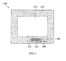
- FIG 2 is a top view diagram of a touch sensing device in accordance with an embodiment of the present disclosure.
- the touch sensing device 500 of the present embodiment comprises a touch panel 200 and a flexible printing circuit board (FPC) 300.
- the touch panel 200 comprises a first bonding mark 208
- the flexible printing circuit board 300 has a bonding surface (not shown) that is bonded to the touch panel 200 and a non-bonding surface 304.
- the flexible printing circuit board 300 further comprises a second bonding mark 308, wherein the second bonding mark 308 is disposed on the non-bonding surface 304 to form a relationship of contraposition with the first bonding mark 208. More particularly, the second bonding mark 308 is disposed on the non-bonding surface 304 with a mode of aligning at the side edge of the flexible printing circuit board 300.
- the touch panel 200 further comprises a visible area 204, a mask area 202 that is surrounding the visible area 204, a bonding area 206, and a terminal wire interface 212.
- the mask area 202 can be formed by coating a mask layer on the substrate of the touch panel 200, and the bonding area 206 is disposed inside the mask area 202.
- the so-called bonding area 206 is defined as an area provided by the touch panel 200 for bonding with the flexible printing circuit board 300.
- the first bonding mark 208 and the terminal wire interface 212 are both further disposed inside the bonding area 206.
- fabricating process of the touch sensing device of the present disclosure is not affected by the mask area 202 on the touch panel 200.
- the fabricating process utilizes the second bonding mark 308 on the non-bonding surface 304 of the flexible printing circuit board 300 to perform contraposition with the first bonding mark 208 disposed on the touch panel 200, wherein shapes and numbers of the first bonding mark 208 and the second bonding mark 308 are not limited by the embodiments of the present disclosure. Shapes and numbers of the first bonding mark 208 and the second bonding mark 308 of the present embodiments that are disclosed by the present specification correspond to each other.
- Shape of the bonding mark can be L-shaped, and multiple first bonding marks 208 and second bonding marks 308 can occur in pairs, which are symmetrically disposed with a left and right mirror reflection, thereby ensuring precision of the contraposition of front, back, left, and right positions.
- first bonding mark 208 and the second bonding mark 308 can also be design as T-shape, cross shape and the like.
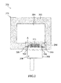
- FIG 3 is a partial enlargement diagram of part A of FIG 2 . More clearly, in FIG. 3 , when the flexible printing circuit board 300 is bonded to the touch panel 200, since the second bonding mark 308 of the flexible printing circuit board 300 is designed on the non-bonding surface 304, the fabricating process can perform the contraposition using an optical sensing device such as charge coupled device (CCD) or naked eye from an angle of top view of FIG 2 , so as to utilize the first bonding mark 208, which has been disposed on preset position of the mask area 202 as a front, back, left and right contraposition benchmarks of the second bonding mark 308. Since the first bonding mark 208 and the second bonding mark 308 of the present embodiment are both designed as L-shaped, the second bonding mark 308 would overlap with a part of the first bonding mark 208.
- CCD charge coupled device
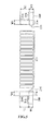
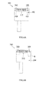
- FIG 4 is a top view diagram of the touch panel 200 in accordance with an embodiment of the present disclosure, which is used for disclosing the back side of the touch panel 200.
- the so-called back side is a surface which would not be touched by users in actual use.
- a terminal wire interface 212 having a fence-like shape, is disposed inside the bonding area 206 as an external electrical connecting interface for the touch panel 200.
- the paired first bonding mark 208 of the present embodiment is symmetrically disposed at two left and right sides of the terminal wire interface 212 with left and right mirror reflection, and respectively separated from the terminal wire interface 212 for a distance. Since the paired first bonding mark 208 has a relationship of left and right mirror reflection, the first bonding mark 208 shown at right side of figure is L-shaped and the first bonding mark 208 shown at left side of figure is reverse L-shaped.
- FIG 5 is a partial enlargement diagram of a bonding area 206 of FIG 4 .
- the first bonding mark 208 has a first base part 216 and at least two first extending parts 214 and 218, wherein one end of first extending parts 214 and 218 respectively connects to two adjacent sides of the first base part 216, and other end respectively extends along different directions to form the L-shaped mark.
- the first extending part 214 extends along a vertical direction and the first extending part 218 extends along a horizontal direction.
- the formed first extending parts 214 and 218 have width W1 and length L1.
- FIG. 6a and FIG 6b are top view diagrams of bonding surface 302 and non-bonding surface 304 of the flexible printing circuit board 300 in accordance with an embodiment of the present disclosure.
- the flexible printing circuit board 300 of the present embodiment can be formed by high polymer translucent material.
- an electrical pin interface 312 having a fence-like shape, is disposed on the bonding surface 302 of the flexible printing circuit board 300 for electrically connecting the terminal wire interface 212 when the flexible printing circuit board 300 is bonded to the touch panel 200, wherein the electrical pin interface 312 can be formed by high polymer transparent material, transparent conductive layer, metal layer, or other known conductive materials.
- the second bonding mark 308 that is designed on the non-bonding surface 304 also has a paired design, and is symmetrically disposed with the left and right mirror reflection. Moreover, space between the paired second bonding mark 308 is corresponding to the space between the paired first bonding mark 208 as shown in FIG. 4 .
- FIG. 7 is a partial enlargement diagram of part B of FIG 6b .
- the second bonding mark 308 comprises a second base part 316 and at least two second extending parts 314 and 318, wherein one end of the second extending parts 314 and 318 is respectively connected to two adjacent sides of the second base part 316, and other end extends along different directions to form the L-shaped mark.
- the second extending part 314 extends along a vertical direction
- the second extending part 318 extends along a horizontal direction.
- the second extending part 314 that extends along the vertical direction is aligned at the side edge 324 of the flexible printing circuit board 300, and the two left and right second extending parts 318 that extend along the horizontal direction are respectively extended to align at the side edges 326 and 328 of the flexible printing circuit board 300.
- the formed second extending parts 314 and 318 have width W2 and length L2.
- width W2 of the second extending parts 314 and 318 of the present embodiment is equal to width W1 of the first extending parts 214 and 218 as shown in FIG 5
- length L1 of the first extending parts 214 and 218 is greater than length L2 of the second extending parts 314 and 318, so that part of first extending parts 214 and 218 can be exposed outside the flexible printing circuit board 300 under the condition that size of the second base part 316 is equal to size of the first base part 216, when the flexible printing circuit board 300 is bonded to the touch panel 200.
- the first bonding mark 208 can achieve the purpose of providing a contraposition benchmark.
- the second extending part 314 (vertical extending) of the second bonding mark 308 and the first extending part 214 (vertical extending) of the first bonding mark 208 are bonding marks for positioning left and right
- the second extending part 318 (horizontal extending) of the second bonding mark 308 and the first extending part 218 (horizontal extending) of the first bonding mark 208 are bonding marks for positioning up and down.
- a third bonding mark 408 is further selectively disposed on the bonding surface 302 of the flexible printing circuit board 300, wherein the third bonding mark 408 is designed as corresponding to at least one part of the second bonding mark 308 on the non-bonding surface 304 of the flexible printing circuit board 300.
- the present disclosure does not limit shape, size, and number of the third bonding mark 408.
- the third bonding mark 408 can be further used for positioning the first bonding mark 208 of the touch panel 200, and usually used for providing a required contraposition benchmark for naked eye.
- the third bonding mark 408 of the present embodiment can be designed as corresponding to shape, size and number of the second base part 316 of the second bonding mark 308. Therefore, in view of the whole touch sensing device 500 after bonding, the first base part 216 of the first bonding mark 208, the second base part 316 of the second bonding mark 308, and the third bonding mark 408 are completely overlapped, wherein the third bonding mark 408 and the first bonding mark 208 are superposed in the structure.
- FIG 8 is a top view diagram of bonding marks of a touch sensing device in accordance with another embodiment of the present disclosure.
- shapes and numbers of first bonding mark 208e and second bonding mark 308e in the present embodiment are also corresponding to each other, and shapes are designed as double L-shape.
- the first bonding mark 208e that disposed on the touch panel 200 can also form a relationship of contraposition with the second bonding mark 308e disposed on the non-bonding surface 304 of the flexible printing circuit board 300, so as to achieve precise front, back, left and right contraposition.
- the present embodiment of FIG 8 can further dispose a third bonding mark 408e on the bonding surface (not shown) of the flexible printing circuit board 300, the design thereof is same as the foregoing embodiment, and not described here again.
- the third bonding mark 408e can be a contraposition benchmark for further positioning the first bonding mark 208e.
- One embodiment of the present disclosure further provides a method of fabricating a touch sensing device. Since the present embodiment is describing the fabricating method based on the embodiments of FIG 3 , 5 and 7 , detailed structure of the touch panel 200 and the flexible printing circuit board 300 are not described here again.
- a touch panel 200 and a flexible printing circuit board 300 are provided, wherein the touch panel 200 comprises a first bonding mark 208, and the flexible printing circuit board 300 has a bonding surface 302 that is bonded to the touch panel 200 and has a non-bonding surface 304, wherein the flexible printing circuit board 300 further comprises a second bonding mark 308 disposed on the non-bonding surface 304.
- a contraposition process is performed from an angle of the non-bonding surface 304 of the flexible printing circuit board 300.
- the contraposition process utilizes the first bonding mark 208 as the contraposition benchmark for the second bonding mark 308. Since lengths of the first extending parts 214 and 218 of the first bonding mark 208 of the present embodiment are respectively greater than that of the second extending parts 314 and 318 of the second bonding mark 308, the second bonding mark 308 would be overlapped with part of the first bonding mark 208 to form a relationship of contraposition.
- the present disclosure can conveniently perform the contraposition by naked eye, and also perform an automatic contraposition and bonding process by using a charge coupled device (CCD), through an improved design of the bonding marks on the touch panel and the flexible printing circuit board. More importantly, in the process of bonding the flexible printing circuit board to a touch panel having a mask area, since the bonding mark of the flexible printing circuit board of the present disclosure is disposed on the non-bonding surface of the flexible printing circuit board, the contraposition performed by the charge coupled device would not be obstructed by the mask area, thereby automatically positioning the bonding mark that is disposed on the touch panel. Overall, the present disclosure can increase the production efficiency, reduce the production cost, and enhance the reliability of the bonding process, thereby improving the production yield of the touch sensing device.
- CCD charge coupled device
Landscapes
- Engineering & Computer Science (AREA)
- Theoretical Computer Science (AREA)
- General Engineering & Computer Science (AREA)
- Human Computer Interaction (AREA)
- Physics & Mathematics (AREA)
- General Physics & Mathematics (AREA)
- Microelectronics & Electronic Packaging (AREA)
- Manufacturing & Machinery (AREA)
- Computer Networks & Wireless Communication (AREA)
- Position Input By Displaying (AREA)
- Push-Button Switches (AREA)
- Combinations Of Printed Boards (AREA)
- Structure Of Printed Boards (AREA)
Applications Claiming Priority (2)
| Application Number | Priority Date | Filing Date | Title |
|---|---|---|---|
| CN201110401077.6A CN103135826B (zh) | 2011-11-27 | 2011-11-27 | 触控感测装置及其制造方法 |
| PCT/CN2012/084426 WO2013075593A1 (zh) | 2011-11-27 | 2012-11-10 | 触控感测装置及其制造方法 |
Publications (2)
| Publication Number | Publication Date |
|---|---|
| EP2784635A1 true EP2784635A1 (de) | 2014-10-01 |
| EP2784635A4 EP2784635A4 (de) | 2016-01-20 |
Family
ID=48469104
Family Applications (1)
| Application Number | Title | Priority Date | Filing Date |
|---|---|---|---|
| EP12852049.1A Withdrawn EP2784635A4 (de) | 2011-11-27 | 2012-11-10 | Berührungsempfindliche vorrichtung und verfahren zu ihrer herstellung |
Country Status (7)
| Country | Link |
|---|---|
| US (1) | US9111706B2 (de) |
| EP (1) | EP2784635A4 (de) |
| JP (1) | JP5940164B2 (de) |
| KR (1) | KR101463306B1 (de) |
| CN (4) | CN106406594B (de) |
| TW (1) | TWI585622B (de) |
| WO (1) | WO2013075593A1 (de) |
Families Citing this family (19)
| Publication number | Priority date | Publication date | Assignee | Title |
|---|---|---|---|---|
| JP2014222438A (ja) * | 2013-05-14 | 2014-11-27 | 株式会社ジャパンディスプレイ | 電子部品及び電子機器 |
| CN104238784B (zh) * | 2013-06-08 | 2018-03-02 | 宸鸿科技(厦门)有限公司 | 触控面板 |
| JP6286911B2 (ja) * | 2013-07-26 | 2018-03-07 | セイコーエプソン株式会社 | 実装構造、電気光学装置及び電子機器 |
| US9367155B2 (en) * | 2013-10-01 | 2016-06-14 | Htc Corporation | Touch panel assembly and electronic device |
| CN104898873A (zh) * | 2014-03-06 | 2015-09-09 | 宝宸(厦门)光学科技有限公司 | 触控面板 |
| JP2015172682A (ja) * | 2014-03-12 | 2015-10-01 | 富士通オプティカルコンポーネンツ株式会社 | 光モジュール |
| KR102237751B1 (ko) * | 2014-12-08 | 2021-04-12 | 삼성디스플레이 주식회사 | 표시 장치 |
| CN106293279A (zh) * | 2015-05-15 | 2017-01-04 | 宝宸(厦门)光学科技有限公司 | 软性电路板及其应用之自电容式触控面板 |
| CN105764278B (zh) * | 2016-02-29 | 2020-04-03 | 上海天马微电子有限公司 | 电子设备及其对位方法 |
| US20170287380A1 (en) * | 2016-04-05 | 2017-10-05 | Shenzhen China Star Optoelectronics Technology Co., Ltd. | Cof structure, driving circuit and display device |
| CN105741678A (zh) * | 2016-04-05 | 2016-07-06 | 深圳市华星光电技术有限公司 | Cof结构、驱动电路及显示装置 |
| CN106094996A (zh) * | 2016-06-23 | 2016-11-09 | 业成光电(深圳)有限公司 | 电子装置 |
| CN106997251B (zh) * | 2017-03-20 | 2020-05-01 | 武汉华星光电技术有限公司 | 含Home键的移动终端及其显示面板 |
| CN110972413B (zh) * | 2018-09-29 | 2023-05-26 | 宏启胜精密电子(秦皇岛)有限公司 | 复合电路板及其制作方法 |
| KR102938608B1 (ko) | 2019-12-13 | 2026-03-13 | 삼성디스플레이 주식회사 | 표시 장치 및 입력 센서 |
| JP7439001B2 (ja) * | 2021-02-19 | 2024-02-27 | 矢崎総業株式会社 | フレキシブルプリント基板、フレキシブルプリント基板の製造方法 |
| CN113437048B (zh) * | 2021-06-28 | 2023-04-07 | 武汉华星光电半导体显示技术有限公司 | 显示装置 |
| TWI789906B (zh) * | 2021-09-13 | 2023-01-11 | 友達光電股份有限公司 | 觸控裝置 |
| CN115172401B (zh) * | 2022-06-23 | 2025-07-29 | 业成光电(深圳)有限公司 | 电路板、显示模组和显示装置 |
Family Cites Families (68)
| Publication number | Priority date | Publication date | Assignee | Title |
|---|---|---|---|---|
| US5592199A (en) * | 1993-01-27 | 1997-01-07 | Sharp Kabushiki Kaisha | Assembly structure of a flat type device including a panel having electrode terminals disposed on a peripheral portion thereof and method for assembling the same |
| JPH07273428A (ja) * | 1994-03-29 | 1995-10-20 | Olympus Optical Co Ltd | レジストパターン形成に基く加工方法並びにレジストパターン作成装置 |
| JP3420391B2 (ja) * | 1995-06-20 | 2003-06-23 | キヤノン株式会社 | 電気回路基板におけるアライメントマーク構造 |
| EP0845697B1 (de) * | 1995-08-07 | 2004-03-17 | Hitachi, Ltd. | Gegen statische elektrizitat unempfindliche flussigkristall-anzeigevorrichtung mit aktiver matrix |
| JP2730572B2 (ja) * | 1996-03-21 | 1998-03-25 | 日本電気株式会社 | 液晶表示装置及びその製造方法 |
| JPH10116862A (ja) * | 1996-10-11 | 1998-05-06 | Texas Instr Japan Ltd | テープキャリアパッケージ |
| JP3407597B2 (ja) * | 1997-05-13 | 2003-05-19 | セイコーエプソン株式会社 | 液晶表示装置、液晶表示パネルの検査方法および液晶表示装置の製造方法 |
| US5876884A (en) * | 1997-10-02 | 1999-03-02 | Fujitsu Limited | Method of fabricating a flat-panel display device and an apparatus therefore |
| US6266119B1 (en) * | 1998-01-13 | 2001-07-24 | Canon Kabushiki Kaisha | Liquid crystal apparatus and production process thereof |
| US6228743B1 (en) * | 1998-05-04 | 2001-05-08 | Motorola, Inc. | Alignment method for semiconductor device |
| KR100522679B1 (ko) * | 1999-07-13 | 2005-10-19 | 삼성에스디아이 주식회사 | 플라즈마 디스플레이장치 |
| JP2000133576A (ja) * | 1998-10-28 | 2000-05-12 | Nec Corp | 位置ずれ計測マーク及び位置ずれ計測方法 |
| TW419720B (en) * | 1999-03-26 | 2001-01-21 | Mosel Vitelic Inc | The method of monitoring the overlay accuracy of the stepper and the device using the same |
| US6498640B1 (en) * | 1999-12-30 | 2002-12-24 | Koninklijke Philips Electronics N.V. | Method to measure alignment using latent image grating structures |
| JP2002032031A (ja) * | 2000-05-12 | 2002-01-31 | Seiko Epson Corp | 電気光学装置の製造方法、端子の接続方法、電気光学装置および電子機器 |
| TWI286629B (en) * | 2000-07-20 | 2007-09-11 | Samsung Electronics Co Ltd | Liquid crystal display device and flexible circuit board |
| US6617702B2 (en) * | 2001-01-25 | 2003-09-09 | Ibm Corporation | Semiconductor device utilizing alignment marks for globally aligning the front and back sides of a semiconductor substrate |
| JP4651886B2 (ja) * | 2001-09-14 | 2011-03-16 | 東北パイオニア株式会社 | 電子機器及び電子機器の製造方法 |
| JP2003131584A (ja) | 2001-10-24 | 2003-05-09 | Seiko Epson Corp | 液晶表示パネル及びその製造方法、液晶表示装置、並びに電子機器 |
| JP3848577B2 (ja) | 2002-01-30 | 2006-11-22 | オプトレックス株式会社 | 可撓配線板 |
| KR100531590B1 (ko) * | 2002-06-06 | 2005-11-28 | 알프스 덴키 가부시키가이샤 | 액정표시장치 및 액정표시장치의 제조방법 |
| JP4047102B2 (ja) * | 2002-08-23 | 2008-02-13 | シャープ株式会社 | フレキシブル基板およびそれを用いたlcdモジュール |
| JP2004111810A (ja) * | 2002-09-20 | 2004-04-08 | Seiko Epson Corp | 複合基板の製造方法、複合基板の構造、電気光学装置及び電子機器 |
| KR100451775B1 (ko) * | 2002-12-31 | 2004-10-08 | 엘지.필립스 엘시디 주식회사 | 터치 패널 |
| JP2004317792A (ja) * | 2003-04-16 | 2004-11-11 | Citizen Watch Co Ltd | 液晶装置 |
| JP4207768B2 (ja) * | 2003-12-16 | 2009-01-14 | セイコーエプソン株式会社 | 電気光学装置並びに電子機器 |
| JP4024773B2 (ja) * | 2004-03-30 | 2007-12-19 | シャープ株式会社 | 配線基板、半導体装置およびその製造方法並びに半導体モジュール装置 |
| TWI249717B (en) * | 2004-04-19 | 2006-02-21 | Au Optronics Corp | Signal transmission device |
| CN1324448C (zh) * | 2004-07-29 | 2007-07-04 | 义隆电子股份有限公司 | 使用薄膜的电容式触控板及其制作方法 |
| JP2006235503A (ja) * | 2005-02-28 | 2006-09-07 | Optrex Corp | 表示装置 |
| JP4854998B2 (ja) * | 2005-07-05 | 2012-01-18 | 三菱電機株式会社 | 液晶表示装置の製造方法 |
| JP4762749B2 (ja) | 2006-02-14 | 2011-08-31 | 日東電工株式会社 | 配線回路基板およびその製造方法 |
| JP2007273578A (ja) * | 2006-03-30 | 2007-10-18 | Optrex Corp | 電子部品接続構造 |
| JP5273330B2 (ja) * | 2006-08-04 | 2013-08-28 | 株式会社ジャパンディスプレイ | 表示装置 |
| KR100780573B1 (ko) * | 2006-08-22 | 2007-11-30 | (주)아이디에스 | 플라스틱 lcd의 ito단과 연성인쇄회로기판의 olb단의 정렬 부착 구조 |
| JP2008112869A (ja) * | 2006-10-30 | 2008-05-15 | Fujitsu Ltd | 組立体モジュールの製造方法および組立体モジュール並びに電子機器 |
| KR101330706B1 (ko) * | 2006-11-03 | 2013-11-19 | 삼성전자주식회사 | 얼라인먼트 마크 |
| JP2008227309A (ja) * | 2007-03-14 | 2008-09-25 | Shinko Electric Ind Co Ltd | 配線基板およびその製造方法 |
| JP5194496B2 (ja) * | 2007-03-14 | 2013-05-08 | パナソニック株式会社 | タッチパネル |
| CN101287329B (zh) * | 2007-04-13 | 2011-04-20 | 群康科技(深圳)有限公司 | 显示装置 |
| CN101842767B (zh) * | 2007-10-31 | 2012-10-03 | 日本写真印刷株式会社 | 电子设备显示窗的带有触摸输入功能的保护面板及电子设备 |
| JP2009231766A (ja) * | 2008-03-25 | 2009-10-08 | Toshiba Corp | マーク形成方法 |
| US8456851B2 (en) * | 2008-05-16 | 2013-06-04 | Apple Inc. | Flex circuit with single sided routing and double sided attach |
| JP2009288276A (ja) * | 2008-05-27 | 2009-12-10 | Seiko Epson Corp | 実装構造体、電気光学装置および電子機器 |
| JP4711149B2 (ja) * | 2008-06-18 | 2011-06-29 | ソニー株式会社 | フレキシブルプリント配線板、タッチパネル、表示パネルおよび表示装置 |
| US20110134075A1 (en) * | 2008-08-07 | 2011-06-09 | Sharp Kabushiki Kaisha | Touch panel, display, and electronic device |
| EP2323466A1 (de) * | 2008-08-11 | 2011-05-18 | Sharp Kabushiki Kaisha | Flexibles substrat und elektrische schaltstruktur |
| CN102187304A (zh) * | 2008-11-19 | 2011-09-14 | 夏普株式会社 | 触摸面板和具备该触摸面板的显示装置 |
| CN201307280Y (zh) * | 2008-11-28 | 2009-09-09 | 深圳市德普特光电显示技术有限公司 | 触摸屏 |
| TWI402566B (zh) * | 2008-12-18 | 2013-07-21 | Chunghwa Picture Tubes Ltd | 具有導線圖案之接墊區以及監控膜材貼附偏差之方法 |
| JP5199189B2 (ja) * | 2009-06-29 | 2013-05-15 | ラピスセミコンダクタ株式会社 | 半導体装置、及び半導体装置の製造方法 |
| JP5345007B2 (ja) * | 2009-06-29 | 2013-11-20 | 株式会社ワコム | 位置検出装置、位置検出回路及び位置検出方法 |
| TWI396004B (zh) * | 2009-08-26 | 2013-05-11 | Au Optronics Corp | 電子裝置 |
| US20110109562A1 (en) * | 2009-11-10 | 2011-05-12 | Teh-Zheng Lin | Decorating frame of touch panel |
| US8786054B2 (en) * | 2009-11-16 | 2014-07-22 | Taiwan Semiconductor Manufacturing Company, Ltd. | Structure for integrated circuit alignment |
| JP5359812B2 (ja) * | 2009-11-24 | 2013-12-04 | セイコーエプソン株式会社 | 電気光学装置、及び電子機器 |
| JP5455034B2 (ja) * | 2009-12-09 | 2014-03-26 | ホシデン株式会社 | フレキシブル配線基板 |
| CN202931661U (zh) * | 2010-03-12 | 2013-05-08 | 夏普株式会社 | 电路基板、基板模块及显示装置 |
| JP5370944B2 (ja) * | 2010-03-17 | 2013-12-18 | 株式会社ジャパンディスプレイ | タッチパネルおよびその製造方法 |
| US8513821B2 (en) * | 2010-05-21 | 2013-08-20 | Taiwan Semiconductor Manufacturing Company, Ltd. | Overlay mark assistant feature |
| US8928159B2 (en) * | 2010-09-02 | 2015-01-06 | Taiwan Semiconductor Manufacturing & Company, Ltd. | Alignment marks in substrate having through-substrate via (TSV) |
| KR101373047B1 (ko) * | 2010-09-07 | 2014-03-11 | 삼성디스플레이 주식회사 | 연성회로기판 및 이를 구비한 터치스크린패널장치 |
| JP5779855B2 (ja) * | 2010-09-24 | 2015-09-16 | 富士通株式会社 | 光モジュールおよび製造方法 |
| KR101969186B1 (ko) * | 2010-09-29 | 2019-04-15 | 다이니폰 인사츠 가부시키가이샤 | 터치스크린 패널 센서 필름 |
| KR101853454B1 (ko) * | 2011-01-21 | 2018-05-02 | 삼성디스플레이 주식회사 | 표시 장치 |
| JP2012222141A (ja) * | 2011-04-08 | 2012-11-12 | Elpida Memory Inc | 半導体チップ |
| CN202422056U (zh) * | 2011-11-27 | 2012-09-05 | 宸鸿科技(厦门)有限公司 | 触控感测装置 |
| KR20130074542A (ko) * | 2011-12-26 | 2013-07-04 | 삼성전기주식회사 | 터치패널의 접합구조체 및 그 제조방법 |
-
2011
- 2011-11-27 CN CN201510552116.0A patent/CN106406594B/zh active Active
- 2011-11-27 CN CN201110401077.6A patent/CN103135826B/zh not_active Expired - Fee Related
- 2011-11-27 CN CN201510551532.9A patent/CN105138172B/zh active Active
- 2011-11-27 CN CN201510552128.3A patent/CN105094447B/zh active Active
-
2012
- 2012-02-15 TW TW101104847A patent/TWI585622B/zh not_active IP Right Cessation
- 2012-11-10 JP JP2014540310A patent/JP5940164B2/ja not_active Expired - Fee Related
- 2012-11-10 EP EP12852049.1A patent/EP2784635A4/de not_active Withdrawn
- 2012-11-10 WO PCT/CN2012/084426 patent/WO2013075593A1/zh not_active Ceased
- 2012-11-20 US US13/682,692 patent/US9111706B2/en active Active
- 2012-11-22 KR KR1020120132810A patent/KR101463306B1/ko not_active Expired - Fee Related
Also Published As
| Publication number | Publication date |
|---|---|
| CN106406594A (zh) | 2017-02-15 |
| US20140139445A1 (en) | 2014-05-22 |
| KR101463306B1 (ko) | 2014-11-18 |
| CN105138172A (zh) | 2015-12-09 |
| JP2015502599A (ja) | 2015-01-22 |
| TWI585622B (zh) | 2017-06-01 |
| CN105094447A (zh) | 2015-11-25 |
| CN103135826A (zh) | 2013-06-05 |
| EP2784635A4 (de) | 2016-01-20 |
| CN105094447B (zh) | 2018-01-16 |
| TW201322077A (zh) | 2013-06-01 |
| WO2013075593A1 (zh) | 2013-05-30 |
| JP5940164B2 (ja) | 2016-06-29 |
| CN106406594B (zh) | 2019-07-16 |
| CN105138172B (zh) | 2018-08-07 |
| US9111706B2 (en) | 2015-08-18 |
| KR20130059279A (ko) | 2013-06-05 |
| CN103135826B (zh) | 2015-10-21 |
Similar Documents
| Publication | Publication Date | Title |
|---|---|---|
| EP2784635A1 (de) | Berührungsempfindliche vorrichtung und verfahren zu ihrer herstellung | |
| CN109521911B (zh) | 一种柔性触控面板及触控显示装置 | |
| US9134828B2 (en) | Touch panel having a shielding structure and method of manufacturing the same | |
| US8803019B2 (en) | Electrode array of touch panel | |
| JP2009169720A (ja) | タッチセンサ | |
| TW201610783A (zh) | 層疊構造體、觸摸面板、帶觸摸面板的顯示裝置及其製造方法 | |
| TWI475461B (zh) | Electrostatic Capacitive Input Device | |
| CN102768599B (zh) | 触控面板 | |
| CN108958539A (zh) | 一种触控显示面板及触控显示装置 | |
| CN102221928B (zh) | 触控显示装置、触控面板以及其制作方法 | |
| JPWO2014050306A1 (ja) | タッチスクリーン | |
| WO2016002645A1 (ja) | タッチパネル基板 | |
| JP6418910B2 (ja) | タッチスクリーン、タッチパネル及び表示装置 | |
| EP3764207A1 (de) | Berührungssubstrat und herstellungsverfahren dafür und anzeigevorrichtung | |
| KR20150092668A (ko) | 터치 윈도우 | |
| JP2013145261A (ja) | タッチパネル及びタッチパネルを備えた表示装置 | |
| CN103631418A (zh) | 触摸屏及触控显示装置 | |
| CN115461702A (zh) | 触控基板和触控显示装置 | |
| JP2013109520A (ja) | タッチパネル | |
| CN102707823A (zh) | 触控感测器 | |
| TWM480233U (zh) | 軟性印刷電路板及其觸控面板 | |
| KR102281616B1 (ko) | 터치 스크린 패널 및 터치 스크린 패널 제조 방법 | |
| CN108415610A (zh) | 一种触控传感器的制备方法和触控传感器 | |
| JP6360312B2 (ja) | 入力装置およびその製造方法 | |
| JP2012018516A (ja) | 入力装置 |
Legal Events
| Date | Code | Title | Description |
|---|---|---|---|
| PUAI | Public reference made under article 153(3) epc to a published international application that has entered the european phase |
Free format text: ORIGINAL CODE: 0009012 |
|
| 17P | Request for examination filed |
Effective date: 20140507 |
|
| AK | Designated contracting states |
Kind code of ref document: A1 Designated state(s): AL AT BE BG CH CY CZ DE DK EE ES FI FR GB GR HR HU IE IS IT LI LT LU LV MC MK MT NL NO PL PT RO RS SE SI SK SM TR |
|
| RIN1 | Information on inventor provided before grant (corrected) |
Inventor name: LUO, JIANXING Inventor name: CHEN, JIADONG Inventor name: HUANG, PINGPING Inventor name: JIANG, YAUCHEN |
|
| DAX | Request for extension of the european patent (deleted) | ||
| RA4 | Supplementary search report drawn up and despatched (corrected) |
Effective date: 20151221 |
|
| RIC1 | Information provided on ipc code assigned before grant |
Ipc: G06F 3/041 20060101AFI20151215BHEP |
|
| STAA | Information on the status of an ep patent application or granted ep patent |
Free format text: STATUS: EXAMINATION IS IN PROGRESS |
|
| 17Q | First examination report despatched |
Effective date: 20180927 |
|
| STAA | Information on the status of an ep patent application or granted ep patent |
Free format text: STATUS: THE APPLICATION IS DEEMED TO BE WITHDRAWN |
|
| 18D | Application deemed to be withdrawn |
Effective date: 20220308 |