EP2719794B1 - Plasma etching of diamond surfaces - Google Patents
Plasma etching of diamond surfaces Download PDFInfo
- Publication number
- EP2719794B1 EP2719794B1 EP13174114.2A EP13174114A EP2719794B1 EP 2719794 B1 EP2719794 B1 EP 2719794B1 EP 13174114 A EP13174114 A EP 13174114A EP 2719794 B1 EP2719794 B1 EP 2719794B1
- Authority
- EP
- European Patent Office
- Prior art keywords
- defects
- less
- diamond
- cvd diamond
- diamond material
- Prior art date
- Legal status (The legal status is an assumption and is not a legal conclusion. Google has not performed a legal analysis and makes no representation as to the accuracy of the status listed.)
- Active
Links
Images


Classifications
-
- C—CHEMISTRY; METALLURGY
- C01—INORGANIC CHEMISTRY
- C01B—NON-METALLIC ELEMENTS; COMPOUNDS THEREOF; METALLOIDS OR COMPOUNDS THEREOF NOT COVERED BY SUBCLASS C01C
- C01B32/00—Carbon; Compounds thereof
- C01B32/25—Diamond
- C01B32/28—After-treatment, e.g. purification, irradiation, separation or recovery
-
- C—CHEMISTRY; METALLURGY
- C23—COATING METALLIC MATERIAL; COATING MATERIAL WITH METALLIC MATERIAL; CHEMICAL SURFACE TREATMENT; DIFFUSION TREATMENT OF METALLIC MATERIAL; COATING BY VACUUM EVAPORATION, BY SPUTTERING, BY ION IMPLANTATION OR BY CHEMICAL VAPOUR DEPOSITION, IN GENERAL; INHIBITING CORROSION OF METALLIC MATERIAL OR INCRUSTATION IN GENERAL
- C23C—COATING METALLIC MATERIAL; COATING MATERIAL WITH METALLIC MATERIAL; SURFACE TREATMENT OF METALLIC MATERIAL BY DIFFUSION INTO THE SURFACE, BY CHEMICAL CONVERSION OR SUBSTITUTION; COATING BY VACUUM EVAPORATION, BY SPUTTERING, BY ION IMPLANTATION OR BY CHEMICAL VAPOUR DEPOSITION, IN GENERAL
- C23C16/00—Chemical coating by decomposition of gaseous compounds, without leaving reaction products of surface material in the coating, i.e. chemical vapour deposition [CVD] processes
- C23C16/22—Chemical coating by decomposition of gaseous compounds, without leaving reaction products of surface material in the coating, i.e. chemical vapour deposition [CVD] processes characterised by the deposition of inorganic material, other than metallic material
- C23C16/26—Deposition of carbon only
- C23C16/27—Diamond only
- C23C16/274—Diamond only using microwave discharges
-
- C—CHEMISTRY; METALLURGY
- C23—COATING METALLIC MATERIAL; COATING MATERIAL WITH METALLIC MATERIAL; CHEMICAL SURFACE TREATMENT; DIFFUSION TREATMENT OF METALLIC MATERIAL; COATING BY VACUUM EVAPORATION, BY SPUTTERING, BY ION IMPLANTATION OR BY CHEMICAL VAPOUR DEPOSITION, IN GENERAL; INHIBITING CORROSION OF METALLIC MATERIAL OR INCRUSTATION IN GENERAL
- C23C—COATING METALLIC MATERIAL; COATING MATERIAL WITH METALLIC MATERIAL; SURFACE TREATMENT OF METALLIC MATERIAL BY DIFFUSION INTO THE SURFACE, BY CHEMICAL CONVERSION OR SUBSTITUTION; COATING BY VACUUM EVAPORATION, BY SPUTTERING, BY ION IMPLANTATION OR BY CHEMICAL VAPOUR DEPOSITION, IN GENERAL
- C23C16/00—Chemical coating by decomposition of gaseous compounds, without leaving reaction products of surface material in the coating, i.e. chemical vapour deposition [CVD] processes
- C23C16/22—Chemical coating by decomposition of gaseous compounds, without leaving reaction products of surface material in the coating, i.e. chemical vapour deposition [CVD] processes characterised by the deposition of inorganic material, other than metallic material
- C23C16/26—Deposition of carbon only
- C23C16/27—Diamond only
- C23C16/278—Diamond only doping or introduction of a secondary phase in the diamond
-
- C—CHEMISTRY; METALLURGY
- C30—CRYSTAL GROWTH
- C30B—SINGLE-CRYSTAL GROWTH; UNIDIRECTIONAL SOLIDIFICATION OF EUTECTIC MATERIAL OR UNIDIRECTIONAL DEMIXING OF EUTECTOID MATERIAL; REFINING BY ZONE-MELTING OF MATERIAL; PRODUCTION OF A HOMOGENEOUS POLYCRYSTALLINE MATERIAL WITH DEFINED STRUCTURE; SINGLE CRYSTALS OR HOMOGENEOUS POLYCRYSTALLINE MATERIAL WITH DEFINED STRUCTURE; AFTER-TREATMENT OF SINGLE CRYSTALS OR A HOMOGENEOUS POLYCRYSTALLINE MATERIAL WITH DEFINED STRUCTURE; APPARATUS THEREFOR
- C30B25/00—Single-crystal growth by chemical reaction of reactive gases, e.g. chemical vapour-deposition growth
- C30B25/02—Epitaxial-layer growth
- C30B25/10—Heating of the reaction chamber or the substrate
- C30B25/105—Heating of the reaction chamber or the substrate by irradiation or electric discharge
-
- C—CHEMISTRY; METALLURGY
- C30—CRYSTAL GROWTH
- C30B—SINGLE-CRYSTAL GROWTH; UNIDIRECTIONAL SOLIDIFICATION OF EUTECTIC MATERIAL OR UNIDIRECTIONAL DEMIXING OF EUTECTOID MATERIAL; REFINING BY ZONE-MELTING OF MATERIAL; PRODUCTION OF A HOMOGENEOUS POLYCRYSTALLINE MATERIAL WITH DEFINED STRUCTURE; SINGLE CRYSTALS OR HOMOGENEOUS POLYCRYSTALLINE MATERIAL WITH DEFINED STRUCTURE; AFTER-TREATMENT OF SINGLE CRYSTALS OR A HOMOGENEOUS POLYCRYSTALLINE MATERIAL WITH DEFINED STRUCTURE; APPARATUS THEREFOR
- C30B25/00—Single-crystal growth by chemical reaction of reactive gases, e.g. chemical vapour-deposition growth
- C30B25/02—Epitaxial-layer growth
- C30B25/18—Epitaxial-layer growth characterised by the substrate
- C30B25/20—Epitaxial-layer growth characterised by the substrate the substrate being of the same materials as the epitaxial layer
-
- C—CHEMISTRY; METALLURGY
- C30—CRYSTAL GROWTH
- C30B—SINGLE-CRYSTAL GROWTH; UNIDIRECTIONAL SOLIDIFICATION OF EUTECTIC MATERIAL OR UNIDIRECTIONAL DEMIXING OF EUTECTOID MATERIAL; REFINING BY ZONE-MELTING OF MATERIAL; PRODUCTION OF A HOMOGENEOUS POLYCRYSTALLINE MATERIAL WITH DEFINED STRUCTURE; SINGLE CRYSTALS OR HOMOGENEOUS POLYCRYSTALLINE MATERIAL WITH DEFINED STRUCTURE; AFTER-TREATMENT OF SINGLE CRYSTALS OR A HOMOGENEOUS POLYCRYSTALLINE MATERIAL WITH DEFINED STRUCTURE; APPARATUS THEREFOR
- C30B29/00—Single crystals or homogeneous polycrystalline material with defined structure characterised by the material or by their shape
- C30B29/02—Elements
- C30B29/04—Diamond
-
- G—PHYSICS
- G01—MEASURING; TESTING
- G01N—INVESTIGATING OR ANALYSING MATERIALS BY DETERMINING THEIR CHEMICAL OR PHYSICAL PROPERTIES
- G01N21/00—Investigating or analysing materials by the use of optical means, i.e. using sub-millimetre waves, infrared, visible or ultraviolet light
- G01N21/84—Systems specially adapted for particular applications
- G01N21/87—Investigating jewels
-
- G—PHYSICS
- G01—MEASURING; TESTING
- G01N—INVESTIGATING OR ANALYSING MATERIALS BY DETERMINING THEIR CHEMICAL OR PHYSICAL PROPERTIES
- G01N21/00—Investigating or analysing materials by the use of optical means, i.e. using sub-millimetre waves, infrared, visible or ultraviolet light
- G01N21/84—Systems specially adapted for particular applications
- G01N21/88—Investigating the presence of flaws or contamination
- G01N21/95—Investigating the presence of flaws or contamination characterised by the material or shape of the object to be examined
-
- G—PHYSICS
- G01—MEASURING; TESTING
- G01N—INVESTIGATING OR ANALYSING MATERIALS BY DETERMINING THEIR CHEMICAL OR PHYSICAL PROPERTIES
- G01N27/00—Investigating or analysing materials by the use of electric, electrochemical, or magnetic means
- G01N27/26—Investigating or analysing materials by the use of electric, electrochemical, or magnetic means by investigating electrochemical variables; by using electrolysis or electrophoresis
- G01N27/28—Electrolytic cell components
- G01N27/30—Electrodes, e.g. test electrodes; Half-cells
- G01N27/308—Electrodes, e.g. test electrodes; Half-cells at least partially made of carbon
-
- H—ELECTRICITY
- H01—ELECTRIC ELEMENTS
- H01J—ELECTRIC DISCHARGE TUBES OR DISCHARGE LAMPS
- H01J37/00—Discharge tubes with provision for introducing objects or material to be exposed to the discharge, e.g. for the purpose of examination or processing thereof
- H01J37/32—Gas-filled discharge tubes
- H01J37/32009—Arrangements for generation of plasma specially adapted for examination or treatment of objects, e.g. plasma sources
- H01J37/32082—Radio frequency generated discharge
- H01J37/321—Radio frequency generated discharge the radio frequency energy being inductively coupled to the plasma
-
- H—ELECTRICITY
- H01—ELECTRIC ELEMENTS
- H01L—SEMICONDUCTOR DEVICES NOT COVERED BY CLASS H10
- H01L21/00—Processes or apparatus adapted for the manufacture or treatment of semiconductor or solid state devices or of parts thereof
- H01L21/02—Manufacture or treatment of semiconductor devices or of parts thereof
- H01L21/02104—Forming layers
- H01L21/02365—Forming inorganic semiconducting materials on a substrate
- H01L21/02367—Substrates
- H01L21/0237—Materials
- H01L21/02373—Group 14 semiconducting materials
- H01L21/02376—Carbon, e.g. diamond-like carbon
-
- H—ELECTRICITY
- H01—ELECTRIC ELEMENTS
- H01L—SEMICONDUCTOR DEVICES NOT COVERED BY CLASS H10
- H01L21/00—Processes or apparatus adapted for the manufacture or treatment of semiconductor or solid state devices or of parts thereof
- H01L21/02—Manufacture or treatment of semiconductor devices or of parts thereof
- H01L21/02104—Forming layers
- H01L21/02365—Forming inorganic semiconducting materials on a substrate
- H01L21/02518—Deposited layers
- H01L21/02521—Materials
- H01L21/02524—Group 14 semiconducting materials
- H01L21/02527—Carbon, e.g. diamond-like carbon
-
- H—ELECTRICITY
- H01—ELECTRIC ELEMENTS
- H01L—SEMICONDUCTOR DEVICES NOT COVERED BY CLASS H10
- H01L21/00—Processes or apparatus adapted for the manufacture or treatment of semiconductor or solid state devices or of parts thereof
- H01L21/02—Manufacture or treatment of semiconductor devices or of parts thereof
- H01L21/02104—Forming layers
- H01L21/02365—Forming inorganic semiconducting materials on a substrate
- H01L21/02518—Deposited layers
- H01L21/0257—Doping during depositing
- H01L21/02573—Conductivity type
- H01L21/02579—P-type
-
- H—ELECTRICITY
- H01—ELECTRIC ELEMENTS
- H01L—SEMICONDUCTOR DEVICES NOT COVERED BY CLASS H10
- H01L21/00—Processes or apparatus adapted for the manufacture or treatment of semiconductor or solid state devices or of parts thereof
- H01L21/02—Manufacture or treatment of semiconductor devices or of parts thereof
- H01L21/02104—Forming layers
- H01L21/02365—Forming inorganic semiconducting materials on a substrate
- H01L21/02612—Formation types
- H01L21/02617—Deposition types
- H01L21/0262—Reduction or decomposition of gaseous compounds, e.g. CVD
-
- H—ELECTRICITY
- H01—ELECTRIC ELEMENTS
- H01L—SEMICONDUCTOR DEVICES NOT COVERED BY CLASS H10
- H01L21/00—Processes or apparatus adapted for the manufacture or treatment of semiconductor or solid state devices or of parts thereof
- H01L21/02—Manufacture or treatment of semiconductor devices or of parts thereof
- H01L21/02104—Forming layers
- H01L21/02365—Forming inorganic semiconducting materials on a substrate
- H01L21/02612—Formation types
- H01L21/02617—Deposition types
- H01L21/02634—Homoepitaxy
-
- H—ELECTRICITY
- H01—ELECTRIC ELEMENTS
- H01L—SEMICONDUCTOR DEVICES NOT COVERED BY CLASS H10
- H01L21/00—Processes or apparatus adapted for the manufacture or treatment of semiconductor or solid state devices or of parts thereof
- H01L21/02—Manufacture or treatment of semiconductor devices or of parts thereof
- H01L21/04—Manufacture or treatment of semiconductor devices or of parts thereof the devices having potential barriers, e.g. a PN junction, depletion layer or carrier concentration layer
- H01L21/0405—Manufacture or treatment of semiconductor devices or of parts thereof the devices having potential barriers, e.g. a PN junction, depletion layer or carrier concentration layer the devices having semiconductor bodies comprising semiconducting carbon, e.g. diamond, diamond-like carbon
- H01L21/041—Making n- or p-doped regions
-
- H—ELECTRICITY
- H10—SEMICONDUCTOR DEVICES; ELECTRIC SOLID-STATE DEVICES NOT OTHERWISE PROVIDED FOR
- H10D—INORGANIC ELECTRIC SEMICONDUCTOR DEVICES
- H10D62/00—Semiconductor bodies, or regions thereof, of devices having potential barriers
- H10D62/40—Crystalline structures
- H10D62/405—Orientations of crystalline planes
-
- H—ELECTRICITY
- H10—SEMICONDUCTOR DEVICES; ELECTRIC SOLID-STATE DEVICES NOT OTHERWISE PROVIDED FOR
- H10D—INORGANIC ELECTRIC SEMICONDUCTOR DEVICES
- H10D62/00—Semiconductor bodies, or regions thereof, of devices having potential barriers
- H10D62/60—Impurity distributions or concentrations
-
- H—ELECTRICITY
- H10—SEMICONDUCTOR DEVICES; ELECTRIC SOLID-STATE DEVICES NOT OTHERWISE PROVIDED FOR
- H10D—INORGANIC ELECTRIC SEMICONDUCTOR DEVICES
- H10D62/00—Semiconductor bodies, or regions thereof, of devices having potential barriers
- H10D62/80—Semiconductor bodies, or regions thereof, of devices having potential barriers characterised by the materials
- H10D62/83—Semiconductor bodies, or regions thereof, of devices having potential barriers characterised by the materials being Group IV materials, e.g. B-doped Si or undoped Ge
- H10D62/8303—Diamond
-
- H—ELECTRICITY
- H10—SEMICONDUCTOR DEVICES; ELECTRIC SOLID-STATE DEVICES NOT OTHERWISE PROVIDED FOR
- H10D—INORGANIC ELECTRIC SEMICONDUCTOR DEVICES
- H10D62/00—Semiconductor bodies, or regions thereof, of devices having potential barriers
- H10D62/80—Semiconductor bodies, or regions thereof, of devices having potential barriers characterised by the materials
- H10D62/83—Semiconductor bodies, or regions thereof, of devices having potential barriers characterised by the materials being Group IV materials, e.g. B-doped Si or undoped Ge
- H10D62/834—Semiconductor bodies, or regions thereof, of devices having potential barriers characterised by the materials being Group IV materials, e.g. B-doped Si or undoped Ge further characterised by the dopants
-
- G—PHYSICS
- G01—MEASURING; TESTING
- G01N—INVESTIGATING OR ANALYSING MATERIALS BY DETERMINING THEIR CHEMICAL OR PHYSICAL PROPERTIES
- G01N2201/00—Features of devices classified in G01N21/00
- G01N2201/06—Illumination; Optics
- G01N2201/063—Illuminating optical parts
- G01N2201/0636—Reflectors
-
- H—ELECTRICITY
- H01—ELECTRIC ELEMENTS
- H01J—ELECTRIC DISCHARGE TUBES OR DISCHARGE LAMPS
- H01J2237/00—Discharge tubes exposing object to beam, e.g. for analysis treatment, etching, imaging
- H01J2237/06—Sources
- H01J2237/08—Ion sources
-
- H—ELECTRICITY
- H01—ELECTRIC ELEMENTS
- H01J—ELECTRIC DISCHARGE TUBES OR DISCHARGE LAMPS
- H01J2237/00—Discharge tubes exposing object to beam, e.g. for analysis treatment, etching, imaging
- H01J2237/32—Processing objects by plasma generation
- H01J2237/33—Processing objects by plasma generation characterised by the type of processing
- H01J2237/334—Etching
- H01J2237/3341—Reactive etching
-
- Y—GENERAL TAGGING OF NEW TECHNOLOGICAL DEVELOPMENTS; GENERAL TAGGING OF CROSS-SECTIONAL TECHNOLOGIES SPANNING OVER SEVERAL SECTIONS OF THE IPC; TECHNICAL SUBJECTS COVERED BY FORMER USPC CROSS-REFERENCE ART COLLECTIONS [XRACs] AND DIGESTS
- Y10—TECHNICAL SUBJECTS COVERED BY FORMER USPC
- Y10T—TECHNICAL SUBJECTS COVERED BY FORMER US CLASSIFICATION
- Y10T428/00—Stock material or miscellaneous articles
- Y10T428/24—Structurally defined web or sheet [e.g., overall dimension, etc.]
- Y10T428/24355—Continuous and nonuniform or irregular surface on layer or component [e.g., roofing, etc.]
Definitions
- the field of the invention is a method of processing diamond surfaces by plasma etching.
- Diamond is a difficult material to form into complex structures because of its hardness and chemical inertness.
- diamond has been shaped by lapidary techniques such as lapping and polishing using fine diamond grits and powders as the abrasive medium.
- One typical product of such processes is faceted natural diamonds used as jewellery.
- Examples of industrial products formed by lapidary processes are polycrystalline diamond plates used as exit windows for high power CO 2 lasers. In all these cases, the finished diamond product has large flat surfaces (i.e. extending laterally greater than a few 10s of micrometers), ostensibly free from surface features which affect the performance.
- Liquid chemical etching processes such as are used extensively in the microelectronics industry are not applicable to diamond because diamond is resistant to almost all chemicals.
- High temperature gas phase etching processes have been used to etch diamond.
- the use of hydrogen-argon-oxygen and hydrogen-argon plasmas at high temperature (>700°C) to etch substrates prior chemical vapour deposition (CVD) diamond synthesis is disclosed in WO 01/96633 .
- Such an etch preferentially etches damage features associated with the sub-surface damage layer and therefore the roughness R q is generally significantly increased as a result of the etch process.
- EP1555337 discloses the use of a reactive ion etch (RIE) using an oxygen-carbon fluoride (O 2 -CF 4 ) gas mixture at a pressure of 1.33-13.3 Pa (about 10-100 mTorr) to prepare mechanically processed single crystal diamond surfaces for CVD growth.
- RIE reactive ion etch
- ICP etching is a largely chemical process in which a plasma is used to breakdown the etching gases into a mixture of free radicals (i.e. neutral species) and ions (i.e. charged species).
- the plasma is remote from the substrate being etched. Between the plasma and the diamond being etched, the vast majority of the ions generated in the plasma are removed. Thus the majority of species that reach the diamond are neutral.
- the resulting etching is therefore largely chemical (e.g. surface reactions leading to volatile products), rather than physical (e.g. sputtering from the surface by ions from the plasma).
- EP0496564 discloses a method for etching diamond using an oxygen plasma.
- Karlsson and Nikolajeff discloses diamond micro-optical structures fabricated by electron-beam lithography and photolithographic methods followed by plasma etching.
- a polycrystalline CVD diamond material according to claim 1 there is provided a polycrystalline CVD diamond material according to claim 1.
- Optional feature are defined in dependent claims.
- a method of producing a diamond surface is described by plasma etching from an original surface which may be prepared by a traditional lapidary process, lapping or polishing or just polishing or from an as-grown surface.
- the invention is directed to a diamond surface, or portion of a diamond surface, which has been produced using the described method.
- a method of producing a diamond surface including the steps of providing an original diamond surface, subjecting the original diamond surface to plasma etching to remove at least 0.5 ⁇ m of material from the original surface and produce a plasma etched surface, the roughness Rq of the plasma etched surface at the location of the etched surface where the greatest depth of material has been removed satisfying at least one of the following conditions:
- a method of producing a diamond surface includes the steps of providing an original diamond surface which has been mechanically processed; and subjecting the original diamond surface to plasma etching to remove at least 0.5 ⁇ m of material from the original surface and produce a plasma etched surface, wherein the plasma etched surface is substantially free from residual damage due to mechanical processing.
- the diamond is polycrystalline CVD diamond.
- the plasma etching utilises an inductively-coupled plasma.
- the gas mixture used in the plasma etching contains argon and chlorine, preferably molecular chlorine (Cl 2 ).
- a method of producing an etched diamond surface including the steps of providing a diamond surface and subjecting the diamond surface to inductively coupled plasma etching using a gas mixture containing argon and chlorine.
- the diamond is polycrystalline CVD diamond according to the claimed invention.
- a polycrystalline CVD diamond material comprising an etched surface or part of an etched surface resulting from at least 0.5 ⁇ m having been removed from a surface or a part of a surface of the diamond by etching, the etched surface having a surface roughness Rq of less than 5 nm.
- the polycrystalline CVD diamond may be for use in an optical device.
- the plasma etching process removes at least 500 nm, preferably at least about 1000 nm, from the original surface or part of the original surface.
- the plasma etching process preferably removes between 500 nm and about 50 ⁇ m, more preferably between 500 nm and about 20 ⁇ m, still more preferably between 500 nm and about 10 ⁇ m, and still more preferably between 500 nm and about 5 ⁇ m from the original surface.
- the plasma etched surface may have a roughness R q A ( A fter the etch) and the original surface a roughness R q B ( B efore the etch), such that R q A /R q B is preferably less than about 1.5, more preferably less than about 1.4, more preferably less than about 1.2, more preferably less than about 1.1.
- R q B is prepared to an R q of less than about 10 nm, more typically less than about 3 nm, more typically less than about 1 nm, more typically less than about 0.5 nm prior to the etch.
- the R q B and R q A measurements are taken on the same area of the diamond.
- standard area is meant an equivalent area as close as reasonably practical, using multiple measurements and statistical analysis where necessary to verify the general validity of the measurements, as is known in the art.
- the particularly unusual advantage of this plasma etch is that it can improve the R q of the diamond surface, particularly when applied to surfaces where the initial surface R q B is prepared to an R q of less than about 1 nm, more typically less than about 0.5 nm, more typically less than about 0.3 nm, thus providing a route to extremely low surface roughness values.
- the plasma etched surface of the invention has a roughness R q A , and the original surface before the etch a roughness, R q B , such that R q A /R q B is less preferably less than about 1.0, more preferably less than about 0.8, more preferably less than about 0.6, more preferably less than about 0.5, more preferably less than about 0.4, more preferably less than about 0.3.
- the method thus provides a plasma etched diamond surface with an R q value preferably less than about 1 nm, preferably less than about 0.5 nm, preferably less than about 0.3 nm, preferably less than about 0.2 nm, preferably less than about 0.1 nm. Furthermore this plasma etched diamond surface with low R q preferably is largely free of processing damage such that the number of defects revealed by the revealing etch test is less than about 100 per mm 2 .
- R q is also known as the 'root mean square' (or RMS) roughness.
- / n
- etc are the moduli of the deviations from the centre-line or plane of the surface profile and n is the number of measurements.
- R a and R q may be measured along lines (a one-dimensional measurement) or over areas (a two-dimensional measurement).
- An area measurement is essentially a series of parallel line measurements.
- the R q value is normally measured over an about 1 ⁇ m by about 1 ⁇ m area or about 2 ⁇ m by about 2 ⁇ m area using a scanning probe instrument such as an atomic force microscope (AFM). In certain circumstances, it is considered more appropriate to measure the R q using a stylus profilometer over a 0.08 mm scan length.
- AFM atomic force microscope
- 'structural feature' or 'topographic feature' is used throughout this specification to refer to desirable features or structure etched into the diamond in a controlled fashion, to provide useful function. In particular this is distinct from features arising in the surface of the diamond from anisotropic etching of sub-surface damage, which are referred to as 'damage features'
- the isotropic nature of the etch of this invention gives surfaces where the presence of any damage features after the etch do not significantly roughen the surface, or more preferably where the etched surface is even smoother than the initially prepared surface, as described above.
- the maximum depth of an etched structural feature in a direction perpendicular to the major surface of the diamond is preferably less than about 20 ⁇ m, more preferably less than about 10 ⁇ m, more preferably less than about 5 ⁇ m, more preferably less than about ⁇ m, more preferably less than about 1 ⁇ m, more preferably less than about 500 nm, more preferably less than about 200 nm, more preferably less than about 100 nm, more preferably less than about 60 nm, and the smallest lateral dimension of the etched structural feature is preferably at least about 0.5 times the maximum depth, more preferably at least about 1 times the maximum depth, more preferably at least about 2 times the maximum depth, more preferably at least about 5 times the maximum depth, more preferably at least about 10 times the maximum depth, more preferably at least about 15 times the maximum depth.
- a method of producing a diamond surface includes the steps of providing an original diamond surface, subjecting the original diamond surface to inductively-coupled plasma etching to remove at least 500 nm of material from the original surface and produce a plasma etched surface, the roughness R q of the plasma etched surface at the location of the etched surface where the greatest depth of material has been removed satisfying at least one of the following conditions:
- the invention provides a polycrystalline CVD diamond comprising an etched surface or part of an etched surface resulting from at least 0.5 ⁇ m having been removed from a surface or a part of a surface of the diamond by etching, the etched surface having a surface roughness R q of less than 5 nm.
- the invention provides a polycrystalline CVD diamond comprising an etched surface or part of an etched surface resulting from at least 0.5 ⁇ m having been removed from a surface or a part of a surface of the diamond by etching, the etched surface having a surface roughness R q of less than 5 nm, preferably less than about 2 nm, preferably less than about 1 nm, preferably less than about 0.5 nm, preferably less than about 0.3 nm, preferably less than about 0.2 nm, preferably less than about 0.1 nm.
- the plasma etched surface can either be in the form of the whole extent of a diamond surface or a proportion of the surface such as structural features etched into the surface as part of the process for making electronic devices, optical elements such as micro-lenses, micro-electro-mechanical systems (MEMS), X-ray optical elements etc.
- optical elements such as micro-lenses, micro-electro-mechanical systems (MEMS), X-ray optical elements etc.
- the method results in a surface or surface structural features that, after undergoing the plasma etching process, are essentially free of the damage characteristic of diamond surfaces prepared by the traditional processes such as lapidary processes of either lapping and polishing or just polishing.
- the extent of sub-surface damage can be revealed and quantified using a deliberately anisotropic thermal revealing etch.
- the revealing etch preferentially oxidises regions of damaged diamond and therefore allows such regions to be identified and thereafter quantified. Regions containing sub-surface damage from mechanical processing are typically darkened or even blackened by the revealing etch.
- the revealing etch consists of:
- the number density of defects is measured by the following method:
- the above method is adapted by completing the defect count over the whole area as a single measurement.
- RBS Rutherford backscattering
- the technique of RBS is well known in the art (for example see the article “ Ion Backscattering Analysis” in “Concise Encyclopedia of Materials Characterization”, Eds R. W. Cahn and E. Lifshin, Pergamon (London), 1993, pages 199-204 ).
- RBS is an ion beam technique that that can probe up to about 1 ⁇ m beneath the surface of a crystalline solid.
- Information about the crystallographic perfection of the near surface layer can be obtained by the use of "channelling", wherein the higher the crystallographic perfection of the surface layer, the lower the backscatter ion yield, such that for a perfect surface, there is substantially no backscattered ion yield (where substantially means less than about 5%, preferably less than about 3%, preferably less than about 2%, preferably less than about 1%, of the incident ions are backscattered).
- the surface of the invention is produced by plasma etching, preferably using an inductively-coupled plasma (ICP) etching process, and preferably at an operating pressure in the range of about 0.5 mTorr (about 0.0667 Pa) to about 100 mTorr (about 13.3 Pa), more preferably in the range of about 1 mTorr (about 0.133 Pa) to about 30 mTorr (about 4.00 Pa), more preferably in the range about 2 mTorr (about 0.267 Pa) to about 10 mTorr (1.33 Pa).
- the etchant is a gas mixture containing argon and chlorine (Cl 2 ).
- chlorine is present in the gas mixture added to the process in a concentration (by volume) in the range about 1% - about 99%, more preferably about 20% - about 85%, more preferably about 40% - about 70%.
- concentration by volume
- the majority of the balance of the gas mixture is made up with Ar, more preferably the whole of the balance of the gas is made up with Ar.
- helium, neon, krypton or xenon, or a mixture of more than one of these may be used in a mixture with argon.
- the plasma etching process is essentially a chemical process, therefore it etches diamond surfaces of all orientations at approximately the same rate, that is, the process can be described as being 'isotropic'. Therefore the process can be used to etch polycrystalline CVD diamond, a polished surface of which typically contains grains in a variety of orientations relative to the surface.
- the method is compatible with conventional lithographic processes that might be used for the fabrication of electronic devices. For example it might be used to produce structural features on the surface of a diamond by applying a suitable resist to the surface, appropriately patterning the resist and then etching the surface using the same ICP process as previously described.
- the method is applied to surfaces comprising synthetic polycrystalline diamond made by CVD techniques ('polycrystalline CVD diamond').
- the plasma etched diamond surface of the present invention can be used for a wide range of applications, including, for example, preparation of substrates for electronic device manufacture free of a damage layer, preparation of substrates for synthesis of homoepitaxial diamond layers by chemical vapour deposition, fabrication of three-dimensional structural features and surface preparation to enable high performance electrical contacts to be made to the surface.
- Diamond can be etched using an Ar-Cl 2 gas mixture.
- Diamond is a highly unreactive solid.
- Halogens are known to stabilise the surface of diamond during CVD growth processes which occur at temperatures between 500°C and 1200°C.
- Inert gases are often used as charged species in PVD etching process, but in ICP the component of etching attributed to charged species is negligible.
- a method of producing an etched diamond surface including the steps of providing a diamond surface and subjecting the diamond surface to inductively coupled plasma etching using a gas mixture containing argon and chlorine.
- the details of the invention will be described using six examples.
- the first example not according to the presently claimed invention, describes making an essentially damage free surface on a series of single crystal CVD diamond plates and comparing the resultant surfaces with a sample that has not been etched.
- the second example describes making fine structural features on a polycrystalline CVD diamond plate. Examples 3 to 6 relate to single crystal diamond samples and are not according to the presently claimed invention.
- the major surfaces of all four plates were initially lapped on a cast iron lapping wheel using progressively finer diamond grit suspended in a cellulose-based carrier.
- the final lapping stage used diamond grit in the size range 15 ⁇ m to 25 ⁇ m and the roughness R q measured using a stylus profilometer over a 0.8 mm length was in the range 100 to 150 nm for all three plates.
- Previous experiments have indicated that after this stage of lapping, the sub-surface damaged layer extends to a depth of approximately 10 ⁇ m beneath the surface.
- All of the plates were chosen at random and their major surfaces were polished using a traditional diamond polishing scaife.
- Two cast iron scaife-wheels were used, the first prepared with diamond powder in the size range 2-4 ⁇ m and the second with diamond powder in the size range 1-2 ⁇ m.
- the depth of material removed during the scaife polishing process was determined to be approximately 15 ⁇ m.
- the R q values measured using a stylus profilometer over an 80 ⁇ m length were less than 5 nm. More accurate measurements over areas (e.g. about 1 ⁇ m by about 1 ⁇ m) made with an atomic force microscope gave the R q values listed in Table 1.
- Example 1' One of the plates (referred to as 'Sample 1') was selected at random and subjected to the thermal revealing etch according to the method previously described (heating the surface in air to about 850°C for 10 seconds using a small air-butane blow torch). The defects were counted according to the method of the invention. The plate showed considerable evidence of sub-surface damage, very much greater than 100 defects per mm 2 .
- the other three plates (referred to as 'Sample 2', 'Sample 3' and 'Sample 4') were subjected to inductively coupled plasma etches to remove material from the surface.
- the ICP etching conditions were: a platen power of approximately 300 W, a coil power of approximately 400 W, a chamber pressure of 5 mTorr (0.667 Pa), flow rates of 25 sccm for Ar and 40 sccm for Cl 2 .
- the etching times chosen for the three samples were 15, 30 and 60 minutes.
- the amount of material removed from the etched surfaces, the initial and final surface roughness, R q , values are in Table 1.
- Micro-trenches were etched into the two samples of polycrystalline diamond using an Ar-Cl 2 ICP plasma.
- Micro-trench photoresist features were mask patterned on the surface of the samples using standard lithographic methods.
- the samples were etched using the following ICP chamber conditions: a platen power of approximately 300 W, a coil power of approximately 400 W, a chamber pressure of 5 mTorr (0.667 Pa), flow rates of 25 sccm for Ar and 40 sccm for Cl 2 .
- a platen power of approximately 300 W
- a coil power of approximately 400 W
- a chamber pressure of 5 mTorr 0.667 Pa
- flow rates 25 sccm for Ar and 40 sccm for Cl 2 .
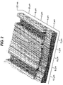
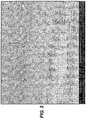
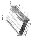
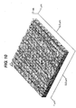
- In the first sample trenches of depth 16 nm were etched [ Figure 1 and Figure 2 ] and in the second sample trenches of depth 53 nm were etched [ Figure 3 and Figure 4 ]. It can be seen that the trench walls are well-defined,
- the etch rates were measured to be approximately 1 nm per second in both cases, which demonstrates the reproducibility of this method. It is also clear that the surfaces post-etch show no indication of the grain boundaries in these polycrystalline samples, which demonstrates that the etch is isotropic in nature.
- the R q , values (measured over 1 ⁇ m x 1 ⁇ m areas using an atomic force microscope) of the samples after etching the 16 and 53 nm deep trenches are 0.8 and 1.1 nm respectively, which should be compared to the pre-etched surface roughness of 1.0 nm. This indicates that under these conditions little or no surface roughening is caused using this etching method, and further supports the conclusion that the etch is isotropic.
- Spherical micro-lens structures were fabricated in a sample of single crystal IIa natural diamond using Ar/Cl 2 ICP etching in conjunction with the photoresist reflow method [ H.W. Choi, E. Gu, C. Liu, J.M. Girkin, M.D. Dawson, J. of Appl. Phys. 97 (6), 063101 (2005 ); C.L. Lee, H.W. Choi, E. Gu, M.D. Dawson, Dia. Rel. Mat. 15, 725 (2006 )].
- a 7 ⁇ m thick layer of Shipley SPR220 photoresist was spin-coated onto the diamond substrate first. After mask patterning, the photoresist pillars were formed.
- the sample was then placed on a hotplate at 125°C for 2 minutes to allow the photoresist pillars to re-flow. Due to the surface tension, spherical lens structures were formed. These lens structures were then transferred onto the diamond substrate by ICP etching using Ar/Cl 2 plasma.
- the ICP parameters used were: a platen power of 100 W, a coil power of 400 W, a chamber pressure of 5 mTorr (0.667 Pa), flow rates of 25 sccm for Ar and 40 sccm for Cl 2 , with an etching duration of 25 minutes.
- FIG. 5 An atomic force microscopy image of a representative diamond micro-lens is shown in Figure 5 .
- the surface diameter and height of the lens were measured to be 50 ⁇ m and 0.75 ⁇ m respectively.
- the profile of the diamond micro-lenses was studied by examining the cross-sectional scan of the atomic force microscopy images. The measured profile was then compared to the curvature of a circle.
- the measured cross-sectional profile of the diamond micro-lens and the fitted spherical profile are plotted in Figure 6 . It can be seen that the deviation from the ideal profile is very small, indicating the cross-sectional profile of the micro-lens is very close to spherical in shape.
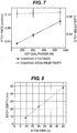
- the etch rate and etch selectivity (as defined earlier) of the Ar/Cl 2 ICP plasma was investigated as a function of the ICP coil power using the following conditions: ICP coil powers of 100 W, 400 W and 900 W; a constant ICP platen power of 300 W; a chamber pressure of 5 mTorr (0.667 Pa); flow rates of 25 sccm for Ar and 40 sccm for Cl 2 ; an etching duration of 5 minutes. Single crystal natural diamond samples were used for these experiments and photoresist was used as the mask material. The results are plotted in Figure 7 . It is observed that the etch rate increases linearly with the ICP coil power and etch selectivity is approximately constant (at around 0.09).
- the etch selectivity on type lb synthetic single crystal diamond was also found to be around 0.09. This should be compared to the etch selectivity using an Ar/O 2 ICP plasma, which is around 0.20 [ C.L. Lee, H.W. Choi, E. Gu, M.D. Dawson, Dia. Rel. Mat. 15, 725 (2006 )].
- the height or depth of microstructures fabricated in diamond such as micro-lenses and micro-trenches
- ICP Ar/Cl 2 etching would be approximately half of those fabricated using ICP Ar/O 2 etching.
- the lower etch selectivity obtained using Ar/Cl 2 is more suitable for etching shallower structural features into diamond in which precise control on the depth or height of the microstructure is required.
- Etch rate as a function of time was investigated by etching micro-trenches in type lb synthetic single crystal diamond samples. Trenches were etched in three samples using identical photoresist masks and under Ar/Cl 2 ICP plasma conditions identical to those described in Example 2. The three samples were etched respectively for 9, 20 and 40 seconds. The depths of the micro-trenches formed were measured by atomic force microscopy and are plotted in Figure 8 as a function of the etch time. The mean etch rate was extracted by performing a simple linear curve fit to the data, and found to be 1.29 ⁇ 0.03 nm s -1 . The small uncertainty in this number indicates that the method yields a reproducible etch rate, which is an important requirement of a manufacturing process.
- Figure 9 shows a representative atomic force microscope scan over a 1 ⁇ m x 1 ⁇ m surface area of the polished sample prior to ICP etching. The surface is characterised by nanometre-scale linear trenches or grooves resulting from the polishing and the roughness R q over this area was measured to be 0.53 nm.
- Figure 10 shows a representative AFM scan over a 1 ⁇ m x 1 ⁇ m surface area of the sample after the ICP etch. It can be seen that the linear polishing grooves are shallower than before and the roughness R q over this area was measured to be 0.19 nm. This example demonstrates the ability of this method to reduce the roughness of mechanically pre-polished diamond surfaces.
Landscapes
- Chemical & Material Sciences (AREA)
- Engineering & Computer Science (AREA)
- Physics & Mathematics (AREA)
- General Physics & Mathematics (AREA)
- Organic Chemistry (AREA)
- Materials Engineering (AREA)
- Manufacturing & Machinery (AREA)
- Power Engineering (AREA)
- Microelectronics & Electronic Packaging (AREA)
- Computer Hardware Design (AREA)
- Condensed Matter Physics & Semiconductors (AREA)
- Chemical Kinetics & Catalysis (AREA)
- Metallurgy (AREA)
- General Chemical & Material Sciences (AREA)
- Life Sciences & Earth Sciences (AREA)
- Inorganic Chemistry (AREA)
- Health & Medical Sciences (AREA)
- Analytical Chemistry (AREA)
- Crystallography & Structural Chemistry (AREA)
- Mechanical Engineering (AREA)
- General Health & Medical Sciences (AREA)
- Pathology (AREA)
- Immunology (AREA)
- Biochemistry (AREA)
- Molecular Biology (AREA)
- Plasma & Fusion (AREA)
- Electrochemistry (AREA)
- Geology (AREA)
- General Life Sciences & Earth Sciences (AREA)
- Crystals, And After-Treatments Of Crystals (AREA)
- Chemical Vapour Deposition (AREA)
- Junction Field-Effect Transistors (AREA)
- Drying Of Semiconductors (AREA)
- Conductive Materials (AREA)
- Battery Electrode And Active Subsutance (AREA)
- Electrodes Of Semiconductors (AREA)
- Carbon And Carbon Compounds (AREA)
Applications Claiming Priority (7)
| Application Number | Priority Date | Filing Date | Title |
|---|---|---|---|
| GB0701186A GB0701186D0 (en) | 2007-01-22 | 2007-01-22 | Electronic field effect devices and methods for their manufacture |
| GB0705524A GB0705524D0 (en) | 2007-03-22 | 2007-03-22 | Plasma etching of diamond surfaces |
| GBGB0705523.9A GB0705523D0 (en) | 2007-01-22 | 2007-03-22 | Diamond electronic devices and methods for their manufacture |
| GBGB0709716.5A GB0709716D0 (en) | 2007-01-22 | 2007-05-21 | Diamond electronic devices including a surface and methods for their manufacture |
| GB0713464A GB0713464D0 (en) | 2007-07-11 | 2007-07-11 | High uniformity boron doped diamond material |
| PCT/IB2008/050215 WO2008090511A1 (en) | 2007-01-22 | 2008-01-22 | Plasma etching of diamond surfaces |
| EP08702485.7A EP2108054B1 (en) | 2007-01-22 | 2008-01-22 | Plasma etching of diamond surfaces |
Related Parent Applications (2)
| Application Number | Title | Priority Date | Filing Date |
|---|---|---|---|
| EP08702485.7A Division EP2108054B1 (en) | 2007-01-22 | 2008-01-22 | Plasma etching of diamond surfaces |
| PCT/IB2008/050215 Previously-Filed-Application WO2008090511A1 (en) | 2007-01-22 | 2008-01-22 | Plasma etching of diamond surfaces |
Publications (3)
| Publication Number | Publication Date |
|---|---|
| EP2719794A2 EP2719794A2 (en) | 2014-04-16 |
| EP2719794A3 EP2719794A3 (en) | 2014-07-09 |
| EP2719794B1 true EP2719794B1 (en) | 2018-08-22 |
Family
ID=39644161
Family Applications (6)
| Application Number | Title | Priority Date | Filing Date |
|---|---|---|---|
| EP13174114.2A Active EP2719794B1 (en) | 2007-01-22 | 2008-01-22 | Plasma etching of diamond surfaces |
| EP08702488A Withdrawn EP2108063A2 (en) | 2007-01-22 | 2008-01-22 | Diamond electronic devices and methods for their manufacture |
| EP08702486.5A Not-in-force EP2108195B1 (en) | 2007-01-22 | 2008-01-22 | Electronic field effect devices and methods for their manufacture |
| EP08702484A Withdrawn EP2118335A1 (en) | 2007-01-22 | 2008-01-22 | High uniformity boron doped diamond material |
| EP08702487A Withdrawn EP2108062A2 (en) | 2007-01-22 | 2008-01-22 | Diamond electronic devices including a surface and methods for their manufacture |
| EP08702485.7A Active EP2108054B1 (en) | 2007-01-22 | 2008-01-22 | Plasma etching of diamond surfaces |
Family Applications After (5)
| Application Number | Title | Priority Date | Filing Date |
|---|---|---|---|
| EP08702488A Withdrawn EP2108063A2 (en) | 2007-01-22 | 2008-01-22 | Diamond electronic devices and methods for their manufacture |
| EP08702486.5A Not-in-force EP2108195B1 (en) | 2007-01-22 | 2008-01-22 | Electronic field effect devices and methods for their manufacture |
| EP08702484A Withdrawn EP2118335A1 (en) | 2007-01-22 | 2008-01-22 | High uniformity boron doped diamond material |
| EP08702487A Withdrawn EP2108062A2 (en) | 2007-01-22 | 2008-01-22 | Diamond electronic devices including a surface and methods for their manufacture |
| EP08702485.7A Active EP2108054B1 (en) | 2007-01-22 | 2008-01-22 | Plasma etching of diamond surfaces |
Country Status (4)
| Country | Link |
|---|---|
| US (8) | US20100038653A1 (enExample) |
| EP (6) | EP2719794B1 (enExample) |
| JP (6) | JP2010517261A (enExample) |
| WO (5) | WO2008090514A2 (enExample) |
Families Citing this family (77)
| Publication number | Priority date | Publication date | Assignee | Title |
|---|---|---|---|---|
| WO2008090514A2 (en) | 2007-01-22 | 2008-07-31 | Element Six Limited | Diamond electronic devices and methods for their manufacture |
| JP5223201B2 (ja) * | 2007-01-29 | 2013-06-26 | 日本電気株式会社 | 電界効果トランジスタ |
| GB0813490D0 (en) | 2008-07-23 | 2008-08-27 | Element Six Ltd | Solid state material |
| GB0813491D0 (en) | 2008-07-23 | 2008-08-27 | Element Six Ltd | Diamond Material |
| GB0816769D0 (en) * | 2008-09-12 | 2008-10-22 | Warwick Ventures | Boron-doped diamond |
| GB0819001D0 (en) | 2008-10-16 | 2008-11-26 | Diamond Detectors Ltd | Contacts on diamond |
| JP5521132B2 (ja) * | 2008-10-20 | 2014-06-11 | 住友電気工業株式会社 | ダイヤモンド電子素子 |
| US20100101010A1 (en) * | 2008-10-24 | 2010-04-29 | Watkins Manufacturing Corporation | Chlorinator for portable spas |
| JP2010161330A (ja) * | 2008-12-08 | 2010-07-22 | Hitachi Cable Ltd | 圧電薄膜素子 |
| WO2010151721A1 (en) * | 2009-06-25 | 2010-12-29 | The Government Of The United States Of America, As Represented By The Secretary Of The Navy | Transistor with enhanced channel charge inducing material layer and threshold voltage control |
| US8266736B2 (en) * | 2009-07-16 | 2012-09-18 | Watkins Manufacturing Corporation | Drop-in chlorinator for portable spas |
| JP5112404B2 (ja) * | 2009-09-01 | 2013-01-09 | 日本電信電話株式会社 | ダイヤモンド電界効果トランジスタ |
| GB2479587A (en) | 2010-04-16 | 2011-10-19 | Diamond Detectors Ltd | Diamond microelectrode |
| FR2959657B1 (fr) * | 2010-05-06 | 2012-06-22 | Commissariat Energie Atomique | Transducteur de variation temporelle de température, puce électronique incorporant ce transducteur et procédé de fabrication de cette puce |
| GB201015270D0 (en) * | 2010-09-14 | 2010-10-27 | Element Six Ltd | Diamond electrodes for electrochemical devices |
| JP5747245B2 (ja) * | 2010-10-14 | 2015-07-08 | 国立研究開発法人物質・材料研究機構 | 電界効果トランジスタ及びその製造方法 |
| GB201021853D0 (en) | 2010-12-23 | 2011-02-02 | Element Six Ltd | A microwave plasma reactor for manufacturing synthetic diamond material |
| GB201021870D0 (en) * | 2010-12-23 | 2011-02-02 | Element Six Ltd | A microwave plasma reactor for manufacturing synthetic diamond material |
| GB201021865D0 (en) | 2010-12-23 | 2011-02-02 | Element Six Ltd | A microwave plasma reactor for manufacturing synthetic diamond material |
| GB201021860D0 (en) | 2010-12-23 | 2011-02-02 | Element Six Ltd | A microwave plasma reactor for diamond synthesis |
| GB201021855D0 (en) | 2010-12-23 | 2011-02-02 | Element Six Ltd | Microwave power delivery system for plasma reactors |
| JP5913362B2 (ja) * | 2010-12-23 | 2016-04-27 | エレメント シックス リミテッド | 合成ダイヤモンド材料のドーピングの制御 |
| GB201021913D0 (en) | 2010-12-23 | 2011-02-02 | Element Six Ltd | Microwave plasma reactors and substrates for synthetic diamond manufacture |
| GB201104579D0 (en) * | 2011-03-18 | 2011-05-04 | Element Six Ltd | Diamond based electrochemical sensors |
| EP2511229B1 (de) * | 2011-04-12 | 2017-03-08 | GFD Gesellschaft für Diamantprodukte mbH | Flankenverstärktes mikromechanisches Bauteil |
| US8624667B2 (en) * | 2011-12-05 | 2014-01-07 | Mitsubishi Electric Research Laboratories, Inc. | High electron mobility transistors with multiple channels |
| JP5759398B2 (ja) * | 2012-02-21 | 2015-08-05 | 日本電信電話株式会社 | ダイヤモンド電界効果トランジスタ及びその作成方法 |
| GB201204388D0 (en) | 2012-03-13 | 2012-04-25 | Element Six Ltd | Synthetic diamond materials for electrochemical sensing applications |
| US9359213B2 (en) * | 2012-06-11 | 2016-06-07 | The Board Of Regents Of The Nevada System Of Higher Education On Behalf Of The University Of Nevada, Las Vegas | Plasma treatment to strengthen diamonds |
| EP2888596B1 (en) * | 2012-08-22 | 2022-07-20 | President and Fellows of Harvard College | Nanoscale scanning sensors |
| WO2014040650A1 (en) | 2012-09-17 | 2014-03-20 | Element Six Limited | Diamond microelectrode |
| GB201310212D0 (en) | 2013-06-07 | 2013-07-24 | Element Six Ltd | Post-synthesis processing of diamond and related super-hard materials |
| GB201322837D0 (en) | 2013-12-23 | 2014-02-12 | Element Six Ltd | Polycrystalline chemical vapour deposited diamond tool parts and methods of fabricating mounting and using the same |
| US10697058B2 (en) * | 2014-07-22 | 2020-06-30 | Sumitomo Electric Industries, Ltd. | Single-crystal diamond, method of producing same, tool including single-crystal diamond, and component including single-crystal diamond |
| CN104233216B (zh) * | 2014-10-09 | 2016-04-20 | 南京航空航天大学 | 一种表面具有纳米结构阵列钛基掺硼金刚石电极的制备方法 |
| US10987735B2 (en) | 2015-12-16 | 2021-04-27 | 6K Inc. | Spheroidal titanium metallic powders with custom microstructures |
| WO2017106601A1 (en) | 2015-12-16 | 2017-06-22 | Amastan Technologies Llc | Spheroidal dehydrogenated metals and metal alloy particles |
| KR102496037B1 (ko) * | 2016-01-20 | 2023-02-06 | 삼성전자주식회사 | 플라즈마 식각 방법 및 장치 |
| US9922791B2 (en) | 2016-05-05 | 2018-03-20 | Arizona Board Of Regents On Behalf Of Arizona State University | Phosphorus doped diamond electrode with tunable low work function for emitter and collector applications |
| US10704160B2 (en) | 2016-05-10 | 2020-07-07 | Arizona Board Of Regents On Behalf Of Arizona State University | Sample stage/holder for improved thermal and gas flow control at elevated growth temperatures |
| US10121657B2 (en) | 2016-05-10 | 2018-11-06 | Arizona Board Of Regents On Behalf Of Arizona State University | Phosphorus incorporation for n-type doping of diamond with (100) and related surface orientation |
| WO2018012529A1 (ja) * | 2016-07-14 | 2018-01-18 | 並木精密宝石株式会社 | 単結晶ダイヤモンド基板 |
| JP6201025B1 (ja) * | 2016-10-14 | 2017-09-20 | 住友化学株式会社 | 偏光子、偏光板及び画像表示装置 |
| US10418475B2 (en) | 2016-11-28 | 2019-09-17 | Arizona Board Of Regents On Behalf Of Arizona State University | Diamond based current aperture vertical transistor and methods of making and using the same |
| US11183390B2 (en) * | 2017-08-15 | 2021-11-23 | Nokomis, Inc. | Method of enhancing a DLC coated surface for enhanced multipaction resistance |
| JP6755223B2 (ja) * | 2017-08-25 | 2020-09-16 | 住友化学株式会社 | 偏光子、偏光板及び画像表示装置 |
| CN107731915B (zh) * | 2017-10-12 | 2024-01-30 | 中国电子科技集团公司第十三研究所 | 半导体器件及利用突变异质结形成金刚石p型导电沟道的方法 |
| DE102018208692A1 (de) | 2018-06-01 | 2019-12-05 | Fraunhofer-Gesellschaft zur Förderung der angewandten Forschung e.V. | Verfahren zur Herstellung homoepitaktischer Diamantschichten |
| EP3810358A1 (en) | 2018-06-19 | 2021-04-28 | 6K Inc. | Process for producing spheroidized powder from feedstock materials |
| EP3830321A1 (en) * | 2018-07-27 | 2021-06-09 | Ecole Polytechnique Federale De Lausanne (Epfl) | Non-contact polishing of a crystalline layer or substrate by ion beam etching |
| GB2582942A (en) * | 2019-04-09 | 2020-10-14 | Element Six Uk Ltd | Boron doped synthetic diamond material |
| CN114007782A (zh) | 2019-04-30 | 2022-02-01 | 6K有限公司 | 机械合金化的粉末原料 |
| US20220254633A1 (en) * | 2019-05-16 | 2022-08-11 | Nippon Telegraph And Telephone Corporation | Semiconductor Layered Structure |
| KR102272513B1 (ko) * | 2019-08-22 | 2021-07-05 | 한국산업기술대학교산학협력단 | 분극에 의한 계면의 고이동도 이차원 전하를 형성하는 방법 및 다이아몬드반도체 접합 소자 |
| US11315951B2 (en) * | 2019-11-11 | 2022-04-26 | Electronics And Telecommunications Research Institute | Semiconductor device and method of fabricating the same |
| JP2023512391A (ja) | 2019-11-18 | 2023-03-27 | シックスケー インコーポレイテッド | 球形粉体用の特異な供給原料及び製造方法 |
| US11590568B2 (en) | 2019-12-19 | 2023-02-28 | 6K Inc. | Process for producing spheroidized powder from feedstock materials |
| CN111647874B (zh) * | 2020-05-11 | 2022-06-21 | 南京岱蒙特科技有限公司 | 一种陶瓷衬底的高比表面积硼掺杂金刚石电极及其制备方法和应用 |
| CN111646633B (zh) * | 2020-05-11 | 2022-11-04 | 南京岱蒙特科技有限公司 | 一种高效节能三维电极有机水处理系统及其处理水的方法 |
| CN111681958A (zh) * | 2020-05-29 | 2020-09-18 | 华南理工大学 | 一种新型异质结构镁扩散制备常关型hemt器件的方法 |
| EP4160660A4 (en) * | 2020-06-01 | 2024-03-20 | Shin-Etsu Handotai Co., Ltd. | METHOD FOR EVALUATION OF THE OUTER PERIPHERAL DISTORTION OF A WAFER |
| AU2021297476A1 (en) | 2020-06-25 | 2022-12-15 | 6K Inc. | Microcomposite alloy structure |
| US11594416B2 (en) * | 2020-08-31 | 2023-02-28 | Applied Materials, Inc. | Tribological properties of diamond films |
| US11963287B2 (en) | 2020-09-24 | 2024-04-16 | 6K Inc. | Systems, devices, and methods for starting plasma |
| JP2023548325A (ja) | 2020-10-30 | 2023-11-16 | シックスケー インコーポレイテッド | 球状化金属粉末の合成のためのシステムおよび方法 |
| CN112795945B (zh) * | 2020-12-10 | 2022-03-08 | 深圳先进技术研究院 | 高臭氧催化活性金刚石电极及其制备方法和应用 |
| AU2022206483A1 (en) | 2021-01-11 | 2023-08-31 | 6K Inc. | Methods and systems for reclamation of li-ion cathode materials using microwave plasma processing |
| EP4313449A1 (en) | 2021-03-31 | 2024-02-07 | 6K Inc. | Systems and methods for additive manufacturing of metal nitride ceramics |
| WO2023229928A1 (en) | 2022-05-23 | 2023-11-30 | 6K Inc. | Microwave plasma apparatus and methods for processing materials using an interior liner |
| US12040162B2 (en) | 2022-06-09 | 2024-07-16 | 6K Inc. | Plasma apparatus and methods for processing feed material utilizing an upstream swirl module and composite gas flows |
| WO2024044498A1 (en) | 2022-08-25 | 2024-02-29 | 6K Inc. | Plasma apparatus and methods for processing feed material utilizing a powder ingress preventor (pip) |
| US12195338B2 (en) | 2022-12-15 | 2025-01-14 | 6K Inc. | Systems, methods, and device for pyrolysis of methane in a microwave plasma for hydrogen and structured carbon powder production |
| GB202219497D0 (en) | 2022-12-22 | 2023-02-08 | Element Six Tech Ltd | Single crystal diamond |
| US12487182B2 (en) * | 2023-05-08 | 2025-12-02 | Tokyo Electron Limited | Non-intrusive method for 2D/3D mapping plasma parameters |
| WO2025186298A1 (en) | 2024-03-05 | 2025-09-12 | Element Six Technologies Limited | Erbium doped single crystal diamond |
| GB202404485D0 (en) | 2024-03-05 | 2024-05-15 | Element Six Tech Ltd | Erbium doped single crystal diamond |
| CN118773573B (zh) * | 2024-09-12 | 2024-11-29 | 北京寰宇晶科科技有限公司 | 一种导电金刚石电极及其制备方法 |
Family Cites Families (74)
| Publication number | Priority date | Publication date | Assignee | Title |
|---|---|---|---|---|
| JPS60246627A (ja) | 1984-05-21 | 1985-12-06 | Sumitomo Electric Ind Ltd | ダイヤモンド半導体素子 |
| JP2542608B2 (ja) | 1987-03-09 | 1996-10-09 | 住友電気工業株式会社 | ダイヤモンド半導体のエツチング方法 |
| GB8812216D0 (en) | 1988-05-24 | 1988-06-29 | Jones B L | Diamond transistor method of manufacture thereof |
| JPH03205339A (ja) | 1989-12-30 | 1991-09-06 | Kawasaki Refract Co Ltd | 炭素含有耐火物 |
| JP2633968B2 (ja) * | 1989-12-30 | 1997-07-23 | キヤノン株式会社 | ダイヤモンド被覆材及びその製造法 |
| JP2913765B2 (ja) | 1990-05-21 | 1999-06-28 | 住友電気工業株式会社 | シヨツトキー接合の形成法 |
| JPH04240725A (ja) | 1991-01-24 | 1992-08-28 | Sumitomo Electric Ind Ltd | エッチング方法 |
| US5173761A (en) | 1991-01-28 | 1992-12-22 | Kobe Steel Usa Inc., Electronic Materials Center | Semiconducting polycrystalline diamond electronic devices employing an insulating diamond layer |
| JPH05139889A (ja) | 1991-11-21 | 1993-06-08 | Canon Inc | ダイヤモンド結晶 |
| JPH05299635A (ja) * | 1992-04-23 | 1993-11-12 | Kobe Steel Ltd | 耐熱性オーミック電極を備えたダイヤモンド薄膜及びその製造方法 |
| US5276338A (en) * | 1992-05-15 | 1994-01-04 | International Business Machines Corporation | Bonded wafer structure having a buried insulation layer |
| US5500077A (en) * | 1993-03-10 | 1996-03-19 | Sumitomo Electric Industries, Ltd. | Method of polishing/flattening diamond |
| JPH0786311A (ja) * | 1993-05-14 | 1995-03-31 | Kobe Steel Ltd | 高配向性ダイヤモンド薄膜電界効果トランジスタ |
| US5371383A (en) * | 1993-05-14 | 1994-12-06 | Kobe Steel Usa Inc. | Highly oriented diamond film field-effect transistor |
| GB2281254B (en) | 1993-08-23 | 1996-11-27 | Northern Telecom Ltd | Polishing polycrystalline films |
| US5609926A (en) * | 1994-03-21 | 1997-03-11 | Prins; Johan F. | Diamond doping |
| JP3309887B2 (ja) | 1994-08-17 | 2002-07-29 | 住友電気工業株式会社 | 半導体装置 |
| US5814194A (en) * | 1994-10-20 | 1998-09-29 | Matsushita Electric Industrial Co., Ltd | Substrate surface treatment method |
| US5711698A (en) | 1995-05-05 | 1998-01-27 | Saint-Gobain/Norton Industrial Ceramics Corp | Method of synthetic diamond ablation with an oxygen plasma and synthetic diamonds etched accordingly |
| US5803967A (en) * | 1995-05-31 | 1998-09-08 | Kobe Steel Usa Inc. | Method of forming diamond devices having textured and highly oriented diamond layers therein |
| US6177292B1 (en) * | 1996-12-05 | 2001-01-23 | Lg Electronics Inc. | Method for forming GaN semiconductor single crystal substrate and GaN diode with the substrate |
| US6013191A (en) * | 1997-10-27 | 2000-01-11 | Advanced Refractory Technologies, Inc. | Method of polishing CVD diamond films by oxygen plasma |
| US6582513B1 (en) * | 1998-05-15 | 2003-06-24 | Apollo Diamond, Inc. | System and method for producing synthetic diamond |
| US6074888A (en) * | 1998-08-18 | 2000-06-13 | Trw Inc. | Method for fabricating semiconductor micro epi-optical components |
| DE19842396A1 (de) * | 1998-09-16 | 2000-04-13 | Fraunhofer Ges Forschung | Elektrode für elektrochemische Prozesse |
| KR100305660B1 (ko) * | 1999-02-09 | 2001-09-26 | 김희용 | 이중이온빔법을 이용하여 CuO를 첨가한 황화합물계 가스 센서 |
| US6508911B1 (en) | 1999-08-16 | 2003-01-21 | Applied Materials Inc. | Diamond coated parts in a plasma reactor |
| US8696875B2 (en) * | 1999-10-08 | 2014-04-15 | Applied Materials, Inc. | Self-ionized and inductively-coupled plasma for sputtering and resputtering |
| US6605352B1 (en) | 2000-01-06 | 2003-08-12 | Saint-Gobain Ceramics & Plastics, Inc. | Corrosion and erosion resistant thin film diamond coating and applications therefor |
| US6652763B1 (en) * | 2000-04-03 | 2003-11-25 | Hrl Laboratories, Llc | Method and apparatus for large-scale diamond polishing |
| EP1292726B8 (en) | 2000-06-15 | 2008-10-29 | Element Six (PTY) Ltd | Single crystal diamond prepared by cvd |
| AU6624601A (en) * | 2000-06-15 | 2001-12-24 | De Beers Ind Diamond | Thick single crystal diamond layer method for making it and gemstones produced from the layer |
| JP2002057167A (ja) | 2000-08-10 | 2002-02-22 | Kobe Steel Ltd | 半導体素子及びその製造方法 |
| JP3908898B2 (ja) | 2000-08-25 | 2007-04-25 | 株式会社神戸製鋼所 | 炭素系材料のエッチング方法 |
| JP2002118257A (ja) | 2000-10-06 | 2002-04-19 | Kobe Steel Ltd | ダイヤモンド半導体装置 |
| US7132309B2 (en) * | 2003-04-22 | 2006-11-07 | Chien-Min Sung | Semiconductor-on-diamond devices and methods of forming |
| JP2002226290A (ja) * | 2000-11-29 | 2002-08-14 | Japan Fine Ceramics Center | ダイヤモンド加工体の製造方法、及び、ダイヤモンド加工体 |
| JP3681340B2 (ja) * | 2001-04-25 | 2005-08-10 | 日本電信電話株式会社 | 電子素子 |
| JP2004538230A (ja) * | 2001-08-08 | 2004-12-24 | アポロ ダイアモンド,インコーポレイティド | 合成ダイヤモンドを生成するためのシステム及び方法 |
| TW525863U (en) * | 2001-10-24 | 2003-03-21 | Polytronics Technology Corp | Electric current overflow protection device |
| GB0130005D0 (en) | 2001-12-14 | 2002-02-06 | Diamanx Products Ltd | Boron doped diamond |
| EP1468438A4 (en) * | 2002-01-03 | 2007-11-21 | Univ Indiana Res & Tech Corp | Simultaneous acquisation of chemical information |
| JP2003347580A (ja) * | 2002-05-28 | 2003-12-05 | Tokyo Gas Co Ltd | ダイヤモンド紫外線発光素子 |
| KR100933847B1 (ko) | 2002-06-18 | 2009-12-24 | 스미토모덴키고교가부시키가이샤 | n형 반도체 다이아몬드 제조 방법 및 반도체 다이아몬드 |
| GB0221949D0 (en) * | 2002-09-20 | 2002-10-30 | Diamanx Products Ltd | Single crystal diamond |
| GB0227261D0 (en) * | 2002-11-21 | 2002-12-31 | Element Six Ltd | Optical quality diamond material |
| JP2004292172A (ja) | 2003-02-04 | 2004-10-21 | Mitsubishi Materials Corp | ダイヤモンド単結晶基材及びその製造方法 |
| JP4076889B2 (ja) * | 2003-03-26 | 2008-04-16 | Tdk株式会社 | 磁気記録媒体の製造方法 |
| JP4683836B2 (ja) * | 2003-12-12 | 2011-05-18 | 株式会社神戸製鋼所 | ダイヤモンド半導体素子及びその製造方法 |
| JP4525897B2 (ja) | 2004-03-22 | 2010-08-18 | 住友電気工業株式会社 | ダイヤモンド単結晶基板 |
| US7481879B2 (en) | 2004-01-16 | 2009-01-27 | Sumitomo Electric Industries, Ltd. | Diamond single crystal substrate manufacturing method and diamond single crystal substrate |
| US7033912B2 (en) | 2004-01-22 | 2006-04-25 | Cree, Inc. | Silicon carbide on diamond substrates and related devices and methods |
| EP1571241A1 (en) | 2004-03-01 | 2005-09-07 | S.O.I.T.E.C. Silicon on Insulator Technologies | Method of manufacturing a wafer |
| US20080117509A1 (en) * | 2004-06-30 | 2008-05-22 | Zeon Corporation | Electromagnetic Wave Shielding Grid Polarizer and Its Manufacturing Method and Grid Polarizer Manufacturing Method |
| EP1779101A1 (en) | 2004-07-27 | 2007-05-02 | Element Six Limited | Diamond electrodes |
| JP4487035B2 (ja) | 2004-09-10 | 2010-06-23 | 凸版印刷株式会社 | ダイヤモンド膜のパターン形成方法 |
| JP4911743B2 (ja) | 2004-09-10 | 2012-04-04 | 独立行政法人物質・材料研究機構 | 電気化学素子及びその製造方法 |
| DE112005002085A5 (de) * | 2004-09-23 | 2007-08-16 | Cemecon Ag | Zerspanungswerkzeug und Verfahren zu seiner Herstellung |
| US7455883B2 (en) | 2004-10-19 | 2008-11-25 | Guardian Industries Corp. | Hydrophilic DLC on substrate with flame pyrolysis treatment |
| JP5362993B2 (ja) | 2004-12-09 | 2013-12-11 | エレメント シックス テクノロジーズ (プロプライアタリー)リミテッド | ダイヤモンド結晶の結晶完全性を改良する方法 |
| JP2008526682A (ja) | 2005-01-11 | 2008-07-24 | アポロ ダイヤモンド,インク | ダイヤモンド製医療装置 |
| JP4582542B2 (ja) | 2005-02-02 | 2010-11-17 | 株式会社神戸製鋼所 | ダイヤモンド電界効果トランジスタ及びその製造方法 |
| JP2006269534A (ja) * | 2005-03-22 | 2006-10-05 | Eudyna Devices Inc | 半導体装置及びその製造方法、その半導体装置製造用基板及びその製造方法並びにその半導体成長用基板 |
| JP5002982B2 (ja) * | 2005-04-15 | 2012-08-15 | 住友電気工業株式会社 | 単結晶ダイヤモンドの製造方法 |
| WO2006114999A1 (ja) * | 2005-04-18 | 2006-11-02 | Kyoto University | 化合物半導体装置及び化合物半導体製造方法 |
| GB0508889D0 (en) * | 2005-04-29 | 2005-06-08 | Element Six Ltd | Diamond transistor and method of manufacture thereof |
| JP2006324465A (ja) * | 2005-05-19 | 2006-11-30 | Matsushita Electric Ind Co Ltd | 半導体装置及びその製造方法 |
| US7964280B2 (en) | 2005-06-22 | 2011-06-21 | Stephen David Williams | High colour diamond layer |
| JP4500745B2 (ja) * | 2005-08-03 | 2010-07-14 | ペルメレック電極株式会社 | 電解用電極の製造方法 |
| JP5323492B2 (ja) | 2005-12-09 | 2013-10-23 | エレメント シックス テクノロジーズ (プロプライアタリー) リミテッド | 高結晶品質の合成ダイヤモンド |
| KR100779078B1 (ko) * | 2005-12-09 | 2007-11-27 | 한국전자통신연구원 | 빛의 방출 효율을 향상시킬 수 있는 실리콘 발광 소자 및그 제조방법 |
| US7557378B2 (en) * | 2006-11-08 | 2009-07-07 | Raytheon Company | Boron aluminum nitride diamond heterostructure |
| GB0700984D0 (en) * | 2007-01-18 | 2007-02-28 | Element Six Ltd | Polycrystalline diamond elements having convex surfaces |
| WO2008090514A2 (en) | 2007-01-22 | 2008-07-31 | Element Six Limited | Diamond electronic devices and methods for their manufacture |
-
2008
- 2008-01-22 WO PCT/IB2008/050219 patent/WO2008090514A2/en not_active Ceased
- 2008-01-22 EP EP13174114.2A patent/EP2719794B1/en active Active
- 2008-01-22 EP EP08702488A patent/EP2108063A2/en not_active Withdrawn
- 2008-01-22 JP JP2009546060A patent/JP2010517261A/ja active Pending
- 2008-01-22 US US12/523,968 patent/US20100038653A1/en not_active Abandoned
- 2008-01-22 WO PCT/IB2008/050216 patent/WO2008090512A1/en not_active Ceased
- 2008-01-22 EP EP08702486.5A patent/EP2108195B1/en not_active Not-in-force
- 2008-01-22 JP JP2009546058A patent/JP5373629B2/ja not_active Expired - Fee Related
- 2008-01-22 WO PCT/IB2008/050215 patent/WO2008090511A1/en not_active Ceased
- 2008-01-22 US US12/523,963 patent/US20100078652A1/en not_active Abandoned
- 2008-01-22 US US12/523,960 patent/US8193538B2/en not_active Expired - Fee Related
- 2008-01-22 JP JP2009546059A patent/JP5341774B2/ja not_active Expired - Fee Related
- 2008-01-22 WO PCT/IB2008/050214 patent/WO2008090510A1/en not_active Ceased
- 2008-01-22 US US12/523,949 patent/US8277622B2/en not_active Expired - Fee Related
- 2008-01-22 EP EP08702484A patent/EP2118335A1/en not_active Withdrawn
- 2008-01-22 EP EP08702487A patent/EP2108062A2/en not_active Withdrawn
- 2008-01-22 WO PCT/IB2008/050218 patent/WO2008090513A2/en not_active Ceased
- 2008-01-22 US US12/523,956 patent/US9034200B2/en active Active
- 2008-01-22 JP JP2009546062A patent/JP2010517263A/ja active Pending
- 2008-01-22 JP JP2009546061A patent/JP5725713B2/ja not_active Expired - Fee Related
- 2008-01-22 EP EP08702485.7A patent/EP2108054B1/en active Active
-
2012
- 2012-05-08 US US13/466,730 patent/US8362492B2/en active Active
- 2012-12-20 US US13/722,857 patent/US8648354B2/en not_active Expired - Fee Related
-
2013
- 2013-04-30 JP JP2013095241A patent/JP5714052B2/ja active Active
-
2015
- 2015-04-13 US US14/685,553 patent/US10011491B2/en active Active
Also Published As
Similar Documents
| Publication | Publication Date | Title |
|---|---|---|
| EP2719794B1 (en) | Plasma etching of diamond surfaces | |
| Forsberg et al. | High aspect ratio optical gratings in diamond | |
| Dussart et al. | Plasma cryogenic etching of silicon: from the early days to today's advanced technologies | |
| KR100857751B1 (ko) | SiC 모니터 웨이퍼의 제조방법 | |
| Ciarlo | Silicon nitride thin windows for biomedical microdevices | |
| Baricordi et al. | Shaping of silicon crystals for channelling experiments through anisotropic chemical etching | |
| US20120205785A1 (en) | Technique for Etching Monolayer and Multilayer Materials | |
| Stognij et al. | Nanoscale ion beam polishing of optical materials | |
| Schmitt et al. | Implementation of smooth nanocrystalline diamond microstructures by combining reactive ion etching and ion beam etching | |
| WO2006059851A1 (en) | Method and apparatus for manufacturing semiconductor | |
| JP2019503969A (ja) | バルク吸収率が低くかつ微小特徴部密度が低い厚手の高光学品質合成多結晶ダイヤモンド材料 | |
| JP4192112B2 (ja) | SiC基板表面の平坦化方法 | |
| JP7526547B2 (ja) | マスクブランク、モールド用マスクブランクの製造方法、及びインプリントモールドの製造方法 | |
| Chutani et al. | Deep Wet-Etched Silicon Cavities for Micro-Optical Sensors: Influence of Masking on $\{111\} $ Sidewalls Surface Quality | |
| US20220275533A1 (en) | Non-contact polishing of a crystalline layer or substrate by ion beam etching | |
| Ralchenko et al. | CVD diamond films on surfaces with intricate shape | |
| Mokhov et al. | Optimization of triangular-profiled Si-grating fabrication technology for EUV and SXR applications | |
| Zeze et al. | Lithography-free high aspect ratio submicron quartz columns by reactive ion etching | |
| Goss et al. | Mechanical lithography using a single point diamond machining | |
| Felgen | Investigation of diamond nanostructures with incorporated color centers | |
| EP1628908A4 (en) | FORMATION OF SILICON NANOSTRUCTURES | |
| Takezawa et al. | Fabrication of a diamond-based imprint mold by applying diamond CVD on silicon master molds for a glass microlens array | |
| EP1241703A1 (en) | Method for masking silicon during anisotropic wet etching | |
| Moronuki et al. | An analysis of surface properties of hetero-epitaxially grown SiC surface on Si substrate | |
| Choi et al. | Orientation-dependent plasma etch rates of single crystal silicon for dry etcher parts |
Legal Events
| Date | Code | Title | Description |
|---|---|---|---|
| PUAI | Public reference made under article 153(3) epc to a published international application that has entered the european phase |
Free format text: ORIGINAL CODE: 0009012 |
|
| 17P | Request for examination filed |
Effective date: 20130627 |
|
| AC | Divisional application: reference to earlier application |
Ref document number: 2108054 Country of ref document: EP Kind code of ref document: P |
|
| AK | Designated contracting states |
Kind code of ref document: A2 Designated state(s): AT BE BG CH CY CZ DE DK EE ES FI FR GB GR HR HU IE IS IT LI LT LU LV MC MT NL NO PL PT RO SE SI SK TR |
|
| PUAL | Search report despatched |
Free format text: ORIGINAL CODE: 0009013 |
|
| AK | Designated contracting states |
Kind code of ref document: A3 Designated state(s): AT BE BG CH CY CZ DE DK EE ES FI FR GB GR HR HU IE IS IT LI LT LU LV MC MT NL NO PL PT RO SE SI SK TR |
|
| RIC1 | Information provided on ipc code assigned before grant |
Ipc: C23C 14/02 20060101ALI20140605BHEP Ipc: C30B 29/04 20060101ALI20140605BHEP Ipc: C30B 25/02 20060101ALI20140605BHEP Ipc: H01L 29/167 20060101ALI20140605BHEP Ipc: H01L 29/16 20060101ALI20140605BHEP Ipc: H01L 21/02 20060101ALI20140605BHEP Ipc: H01L 29/04 20060101ALI20140605BHEP Ipc: C23C 14/58 20060101AFI20140605BHEP Ipc: C30B 25/10 20060101ALI20140605BHEP Ipc: G01N 27/30 20060101ALI20140605BHEP Ipc: H01L 21/04 20060101ALI20140605BHEP Ipc: C30B 25/20 20060101ALI20140605BHEP Ipc: C23C 16/27 20060101ALI20140605BHEP Ipc: C23C 16/56 20060101ALI20140605BHEP Ipc: H01L 29/36 20060101ALI20140605BHEP |
|
| RAP1 | Party data changed (applicant data changed or rights of an application transferred) |
Owner name: ELEMENT SIX TECHNOLOGIES LIMITED |
|
| RBV | Designated contracting states (corrected) |
Designated state(s): AT BE BG CH CY CZ DE DK EE ES FI FR GB GR HR HU IE IS IT LI LT LU LV MC MT NL NO PL PT RO SE SI SK TR |
|
| STAA | Information on the status of an ep patent application or granted ep patent |
Free format text: STATUS: EXAMINATION IS IN PROGRESS |
|
| 17Q | First examination report despatched |
Effective date: 20170718 |
|
| REG | Reference to a national code |
Ref country code: DE Ref legal event code: R079 Ref document number: 602008056654 Country of ref document: DE Free format text: PREVIOUS MAIN CLASS: C23C0014580000 Ipc: C30B0025200000 |
|
| RIC1 | Information provided on ipc code assigned before grant |
Ipc: H01L 21/02 20060101ALI20180213BHEP Ipc: H01L 29/04 20060101ALI20180213BHEP Ipc: C23C 16/27 20060101ALI20180213BHEP Ipc: H01L 29/16 20060101ALI20180213BHEP Ipc: H01L 21/04 20060101ALI20180213BHEP Ipc: H01L 29/167 20060101ALI20180213BHEP Ipc: C01B 32/28 20170101ALI20180213BHEP Ipc: C30B 29/04 20060101ALI20180213BHEP Ipc: G01N 27/30 20060101ALI20180213BHEP Ipc: H01L 29/36 20060101ALI20180213BHEP Ipc: H01J 37/32 20060101ALI20180213BHEP Ipc: C30B 25/20 20060101AFI20180213BHEP Ipc: C30B 25/10 20060101ALI20180213BHEP |
|
| GRAP | Despatch of communication of intention to grant a patent |
Free format text: ORIGINAL CODE: EPIDOSNIGR1 |
|
| STAA | Information on the status of an ep patent application or granted ep patent |
Free format text: STATUS: GRANT OF PATENT IS INTENDED |
|
| INTG | Intention to grant announced |
Effective date: 20180322 |
|
| GRAS | Grant fee paid |
Free format text: ORIGINAL CODE: EPIDOSNIGR3 |
|
| GRAA | (expected) grant |
Free format text: ORIGINAL CODE: 0009210 |
|
| STAA | Information on the status of an ep patent application or granted ep patent |
Free format text: STATUS: THE PATENT HAS BEEN GRANTED |
|
| AC | Divisional application: reference to earlier application |
Ref document number: 2108054 Country of ref document: EP Kind code of ref document: P |
|
| AK | Designated contracting states |
Kind code of ref document: B1 Designated state(s): AT BE BG CH CY CZ DE DK EE ES FI FR GB GR HR HU IE IS IT LI LT LU LV MC MT NL NO PL PT RO SE SI SK TR |
|
| REG | Reference to a national code |
Ref country code: GB Ref legal event code: FG4D |
|
| REG | Reference to a national code |
Ref country code: CH Ref legal event code: EP |
|
| REG | Reference to a national code |
Ref country code: AT Ref legal event code: REF Ref document number: 1032624 Country of ref document: AT Kind code of ref document: T Effective date: 20180915 |
|
| REG | Reference to a national code |
Ref country code: IE Ref legal event code: FG4D |
|
| REG | Reference to a national code |
Ref country code: DE Ref legal event code: R096 Ref document number: 602008056654 Country of ref document: DE |
|
| REG | Reference to a national code |
Ref country code: NL Ref legal event code: MP Effective date: 20180822 |
|
| REG | Reference to a national code |
Ref country code: LT Ref legal event code: MG4D |
|
| PG25 | Lapsed in a contracting state [announced via postgrant information from national office to epo] |
Ref country code: FI Free format text: LAPSE BECAUSE OF FAILURE TO SUBMIT A TRANSLATION OF THE DESCRIPTION OR TO PAY THE FEE WITHIN THE PRESCRIBED TIME-LIMIT Effective date: 20180822 Ref country code: LT Free format text: LAPSE BECAUSE OF FAILURE TO SUBMIT A TRANSLATION OF THE DESCRIPTION OR TO PAY THE FEE WITHIN THE PRESCRIBED TIME-LIMIT Effective date: 20180822 Ref country code: NL Free format text: LAPSE BECAUSE OF FAILURE TO SUBMIT A TRANSLATION OF THE DESCRIPTION OR TO PAY THE FEE WITHIN THE PRESCRIBED TIME-LIMIT Effective date: 20180822 Ref country code: BG Free format text: LAPSE BECAUSE OF FAILURE TO SUBMIT A TRANSLATION OF THE DESCRIPTION OR TO PAY THE FEE WITHIN THE PRESCRIBED TIME-LIMIT Effective date: 20181122 Ref country code: IS Free format text: LAPSE BECAUSE OF FAILURE TO SUBMIT A TRANSLATION OF THE DESCRIPTION OR TO PAY THE FEE WITHIN THE PRESCRIBED TIME-LIMIT Effective date: 20181222 Ref country code: NO Free format text: LAPSE BECAUSE OF FAILURE TO SUBMIT A TRANSLATION OF THE DESCRIPTION OR TO PAY THE FEE WITHIN THE PRESCRIBED TIME-LIMIT Effective date: 20181122 Ref country code: GR Free format text: LAPSE BECAUSE OF FAILURE TO SUBMIT A TRANSLATION OF THE DESCRIPTION OR TO PAY THE FEE WITHIN THE PRESCRIBED TIME-LIMIT Effective date: 20181123 Ref country code: SE Free format text: LAPSE BECAUSE OF FAILURE TO SUBMIT A TRANSLATION OF THE DESCRIPTION OR TO PAY THE FEE WITHIN THE PRESCRIBED TIME-LIMIT Effective date: 20180822 |
|
| REG | Reference to a national code |
Ref country code: AT Ref legal event code: MK05 Ref document number: 1032624 Country of ref document: AT Kind code of ref document: T Effective date: 20180822 |
|
| PG25 | Lapsed in a contracting state [announced via postgrant information from national office to epo] |
Ref country code: LV Free format text: LAPSE BECAUSE OF FAILURE TO SUBMIT A TRANSLATION OF THE DESCRIPTION OR TO PAY THE FEE WITHIN THE PRESCRIBED TIME-LIMIT Effective date: 20180822 Ref country code: HR Free format text: LAPSE BECAUSE OF FAILURE TO SUBMIT A TRANSLATION OF THE DESCRIPTION OR TO PAY THE FEE WITHIN THE PRESCRIBED TIME-LIMIT Effective date: 20180822 |
|
| PG25 | Lapsed in a contracting state [announced via postgrant information from national office to epo] |
Ref country code: IT Free format text: LAPSE BECAUSE OF FAILURE TO SUBMIT A TRANSLATION OF THE DESCRIPTION OR TO PAY THE FEE WITHIN THE PRESCRIBED TIME-LIMIT Effective date: 20180822 Ref country code: PL Free format text: LAPSE BECAUSE OF FAILURE TO SUBMIT A TRANSLATION OF THE DESCRIPTION OR TO PAY THE FEE WITHIN THE PRESCRIBED TIME-LIMIT Effective date: 20180822 Ref country code: EE Free format text: LAPSE BECAUSE OF FAILURE TO SUBMIT A TRANSLATION OF THE DESCRIPTION OR TO PAY THE FEE WITHIN THE PRESCRIBED TIME-LIMIT Effective date: 20180822 Ref country code: AT Free format text: LAPSE BECAUSE OF FAILURE TO SUBMIT A TRANSLATION OF THE DESCRIPTION OR TO PAY THE FEE WITHIN THE PRESCRIBED TIME-LIMIT Effective date: 20180822 Ref country code: ES Free format text: LAPSE BECAUSE OF FAILURE TO SUBMIT A TRANSLATION OF THE DESCRIPTION OR TO PAY THE FEE WITHIN THE PRESCRIBED TIME-LIMIT Effective date: 20180822 Ref country code: CZ Free format text: LAPSE BECAUSE OF FAILURE TO SUBMIT A TRANSLATION OF THE DESCRIPTION OR TO PAY THE FEE WITHIN THE PRESCRIBED TIME-LIMIT Effective date: 20180822 Ref country code: RO Free format text: LAPSE BECAUSE OF FAILURE TO SUBMIT A TRANSLATION OF THE DESCRIPTION OR TO PAY THE FEE WITHIN THE PRESCRIBED TIME-LIMIT Effective date: 20180822 |
|
| REG | Reference to a national code |
Ref country code: DE Ref legal event code: R097 Ref document number: 602008056654 Country of ref document: DE |
|
| PG25 | Lapsed in a contracting state [announced via postgrant information from national office to epo] |
Ref country code: DK Free format text: LAPSE BECAUSE OF FAILURE TO SUBMIT A TRANSLATION OF THE DESCRIPTION OR TO PAY THE FEE WITHIN THE PRESCRIBED TIME-LIMIT Effective date: 20180822 Ref country code: SK Free format text: LAPSE BECAUSE OF FAILURE TO SUBMIT A TRANSLATION OF THE DESCRIPTION OR TO PAY THE FEE WITHIN THE PRESCRIBED TIME-LIMIT Effective date: 20180822 |
|
| PLBE | No opposition filed within time limit |
Free format text: ORIGINAL CODE: 0009261 |
|
| STAA | Information on the status of an ep patent application or granted ep patent |
Free format text: STATUS: NO OPPOSITION FILED WITHIN TIME LIMIT |
|
| 26N | No opposition filed |
Effective date: 20190523 |
|
| PG25 | Lapsed in a contracting state [announced via postgrant information from national office to epo] |
Ref country code: MC Free format text: LAPSE BECAUSE OF FAILURE TO SUBMIT A TRANSLATION OF THE DESCRIPTION OR TO PAY THE FEE WITHIN THE PRESCRIBED TIME-LIMIT Effective date: 20180822 Ref country code: SI Free format text: LAPSE BECAUSE OF FAILURE TO SUBMIT A TRANSLATION OF THE DESCRIPTION OR TO PAY THE FEE WITHIN THE PRESCRIBED TIME-LIMIT Effective date: 20180822 |
|
| REG | Reference to a national code |
Ref country code: CH Ref legal event code: PL |
|
| PG25 | Lapsed in a contracting state [announced via postgrant information from national office to epo] |
Ref country code: LU Free format text: LAPSE BECAUSE OF NON-PAYMENT OF DUE FEES Effective date: 20190122 |
|
| REG | Reference to a national code |
Ref country code: BE Ref legal event code: MM Effective date: 20190131 |
|
| REG | Reference to a national code |
Ref country code: IE Ref legal event code: MM4A |
|
| PG25 | Lapsed in a contracting state [announced via postgrant information from national office to epo] |
Ref country code: FR Free format text: LAPSE BECAUSE OF NON-PAYMENT OF DUE FEES Effective date: 20190131 |
|
| PG25 | Lapsed in a contracting state [announced via postgrant information from national office to epo] |
Ref country code: BE Free format text: LAPSE BECAUSE OF NON-PAYMENT OF DUE FEES Effective date: 20190131 |
|
| PG25 | Lapsed in a contracting state [announced via postgrant information from national office to epo] |
Ref country code: LI Free format text: LAPSE BECAUSE OF NON-PAYMENT OF DUE FEES Effective date: 20190131 Ref country code: CH Free format text: LAPSE BECAUSE OF NON-PAYMENT OF DUE FEES Effective date: 20190131 |
|
| PG25 | Lapsed in a contracting state [announced via postgrant information from national office to epo] |
Ref country code: IE Free format text: LAPSE BECAUSE OF NON-PAYMENT OF DUE FEES Effective date: 20190122 |
|
| PG25 | Lapsed in a contracting state [announced via postgrant information from national office to epo] |
Ref country code: TR Free format text: LAPSE BECAUSE OF FAILURE TO SUBMIT A TRANSLATION OF THE DESCRIPTION OR TO PAY THE FEE WITHIN THE PRESCRIBED TIME-LIMIT Effective date: 20180822 |
|
| PG25 | Lapsed in a contracting state [announced via postgrant information from national office to epo] |
Ref country code: MT Free format text: LAPSE BECAUSE OF NON-PAYMENT OF DUE FEES Effective date: 20190122 Ref country code: PT Free format text: LAPSE BECAUSE OF FAILURE TO SUBMIT A TRANSLATION OF THE DESCRIPTION OR TO PAY THE FEE WITHIN THE PRESCRIBED TIME-LIMIT Effective date: 20181222 |
|
| PG25 | Lapsed in a contracting state [announced via postgrant information from national office to epo] |
Ref country code: CY Free format text: LAPSE BECAUSE OF FAILURE TO SUBMIT A TRANSLATION OF THE DESCRIPTION OR TO PAY THE FEE WITHIN THE PRESCRIBED TIME-LIMIT Effective date: 20180822 |
|
| PG25 | Lapsed in a contracting state [announced via postgrant information from national office to epo] |
Ref country code: HU Free format text: LAPSE BECAUSE OF FAILURE TO SUBMIT A TRANSLATION OF THE DESCRIPTION OR TO PAY THE FEE WITHIN THE PRESCRIBED TIME-LIMIT; INVALID AB INITIO Effective date: 20080122 |
|
| P01 | Opt-out of the competence of the unified patent court (upc) registered |
Effective date: 20230524 |
|
| PGFP | Annual fee paid to national office [announced via postgrant information from national office to epo] |
Ref country code: DE Payment date: 20250129 Year of fee payment: 18 |
|
| PGFP | Annual fee paid to national office [announced via postgrant information from national office to epo] |
Ref country code: GB Payment date: 20250127 Year of fee payment: 18 |