EP2650399B1 - High temperature atomic layer deposition of silicon oxide thin films - Google Patents
High temperature atomic layer deposition of silicon oxide thin films Download PDFInfo
- Publication number
- EP2650399B1 EP2650399B1 EP13163586.4A EP13163586A EP2650399B1 EP 2650399 B1 EP2650399 B1 EP 2650399B1 EP 13163586 A EP13163586 A EP 13163586A EP 2650399 B1 EP2650399 B1 EP 2650399B1
- Authority
- EP
- European Patent Office
- Prior art keywords
- group
- reactor
- silicon
- precursor
- deposition
- Prior art date
- Legal status (The legal status is an assumption and is not a legal conclusion. Google has not performed a legal analysis and makes no representation as to the accuracy of the status listed.)
- Active
Links
- VYPSYNLAJGMNEJ-UHFFFAOYSA-N Silicium dioxide Chemical group O=[Si]=O VYPSYNLAJGMNEJ-UHFFFAOYSA-N 0.000 title claims description 90
- 229910052814 silicon oxide Inorganic materials 0.000 title claims description 41
- 238000000231 atomic layer deposition Methods 0.000 title description 59
- 239000010409 thin film Substances 0.000 title description 2
- 238000000034 method Methods 0.000 claims description 86
- 238000010926 purge Methods 0.000 claims description 66
- 239000012686 silicon precursor Substances 0.000 claims description 52
- QVGXLLKOCUKJST-UHFFFAOYSA-N atomic oxygen Chemical compound [O] QVGXLLKOCUKJST-UHFFFAOYSA-N 0.000 claims description 46
- 239000001301 oxygen Substances 0.000 claims description 46
- 229910052760 oxygen Inorganic materials 0.000 claims description 46
- 239000007789 gas Substances 0.000 claims description 45
- 239000002243 precursor Substances 0.000 claims description 40
- IJGRMHOSHXDMSA-UHFFFAOYSA-N Atomic nitrogen Chemical compound N#N IJGRMHOSHXDMSA-UHFFFAOYSA-N 0.000 claims description 37
- 239000000758 substrate Substances 0.000 claims description 25
- XLYOFNOQVPJJNP-UHFFFAOYSA-N water Chemical compound O XLYOFNOQVPJJNP-UHFFFAOYSA-N 0.000 claims description 25
- CBENFWSGALASAD-UHFFFAOYSA-N Ozone Chemical compound [O-][O+]=O CBENFWSGALASAD-UHFFFAOYSA-N 0.000 claims description 21
- 125000002496 methyl group Chemical group [H]C([H])([H])* 0.000 claims description 21
- 239000000203 mixture Substances 0.000 claims description 21
- KAHVZNKZQFSBFW-UHFFFAOYSA-N n-methyl-n-trimethylsilylmethanamine Chemical compound CN(C)[Si](C)(C)C KAHVZNKZQFSBFW-UHFFFAOYSA-N 0.000 claims description 21
- 229910052757 nitrogen Inorganic materials 0.000 claims description 19
- 125000003118 aryl group Chemical group 0.000 claims description 17
- 125000004122 cyclic group Chemical group 0.000 claims description 16
- XKRFYHLGVUSROY-UHFFFAOYSA-N Argon Chemical compound [Ar] XKRFYHLGVUSROY-UHFFFAOYSA-N 0.000 claims description 12
- MHAJPDPJQMAIIY-UHFFFAOYSA-N Hydrogen peroxide Chemical compound OO MHAJPDPJQMAIIY-UHFFFAOYSA-N 0.000 claims description 12
- 125000000008 (C1-C10) alkyl group Chemical group 0.000 claims description 11
- JOOMLFKONHCLCJ-UHFFFAOYSA-N N-(trimethylsilyl)diethylamine Chemical group CCN(CC)[Si](C)(C)C JOOMLFKONHCLCJ-UHFFFAOYSA-N 0.000 claims description 11
- XUIMIQQOPSSXEZ-UHFFFAOYSA-N Silicon Chemical compound [Si] XUIMIQQOPSSXEZ-UHFFFAOYSA-N 0.000 claims description 11
- 229910052710 silicon Inorganic materials 0.000 claims description 10
- 239000001257 hydrogen Substances 0.000 claims description 9
- 229910052739 hydrogen Inorganic materials 0.000 claims description 9
- 239000010703 silicon Substances 0.000 claims description 9
- IJOOHPMOJXWVHK-UHFFFAOYSA-N chlorotrimethylsilane Chemical compound C[Si](C)(C)Cl IJOOHPMOJXWVHK-UHFFFAOYSA-N 0.000 claims description 8
- FFUAGWLWBBFQJT-UHFFFAOYSA-N hexamethyldisilazane Chemical group C[Si](C)(C)N[Si](C)(C)C FFUAGWLWBBFQJT-UHFFFAOYSA-N 0.000 claims description 8
- 125000004435 hydrogen atom Chemical group [H]* 0.000 claims description 8
- NFVBAYVEVKKWEE-UHFFFAOYSA-N (2,6-dimethylpiperidin-1-yl)-trimethylsilane Chemical compound CC1CCCC(C)N1[Si](C)(C)C NFVBAYVEVKKWEE-UHFFFAOYSA-N 0.000 claims description 7
- 125000005103 alkyl silyl group Chemical group 0.000 claims description 7
- 125000002887 hydroxy group Chemical group [H]O* 0.000 claims description 7
- GQPLMRYTRLFLPF-UHFFFAOYSA-N Nitrous Oxide Chemical compound [O-][N+]#N GQPLMRYTRLFLPF-UHFFFAOYSA-N 0.000 claims description 6
- 229910052786 argon Inorganic materials 0.000 claims description 6
- 150000004820 halides Chemical group 0.000 claims description 6
- 229910052794 bromium Inorganic materials 0.000 claims description 4
- 229910052801 chlorine Inorganic materials 0.000 claims description 4
- 229910052734 helium Inorganic materials 0.000 claims description 4
- 239000001307 helium Substances 0.000 claims description 4
- SWQJXJOGLNCZEY-UHFFFAOYSA-N helium atom Chemical compound [He] SWQJXJOGLNCZEY-UHFFFAOYSA-N 0.000 claims description 4
- 229910052740 iodine Inorganic materials 0.000 claims description 4
- POPACFLNWGUDSR-UHFFFAOYSA-N methoxy(trimethyl)silane Chemical group CO[Si](C)(C)C POPACFLNWGUDSR-UHFFFAOYSA-N 0.000 claims description 4
- KFQPFPKLVQBQBZ-UHFFFAOYSA-N (2,5-dimethylpyrrolidin-1-yl)-trimethylsilane Chemical compound CC1CCC(C)N1[Si](C)(C)C KFQPFPKLVQBQBZ-UHFFFAOYSA-N 0.000 claims description 2
- AALRHBLMAVGWRR-UHFFFAOYSA-N 1-chlorobutan-2-one Chemical compound CCC(=O)CCl AALRHBLMAVGWRR-UHFFFAOYSA-N 0.000 claims description 2
- GVHIREZHTRULPT-UHFFFAOYSA-N 2-methyl-n-trimethylsilylpropan-2-amine Chemical compound CC(C)(C)N[Si](C)(C)C GVHIREZHTRULPT-UHFFFAOYSA-N 0.000 claims description 2
- 125000002252 acyl group Chemical group 0.000 claims description 2
- RSIHJDGMBDPTIM-UHFFFAOYSA-N ethoxy(trimethyl)silane Chemical compound CCO[Si](C)(C)C RSIHJDGMBDPTIM-UHFFFAOYSA-N 0.000 claims description 2
- OGWVYCFORNDBRE-UHFFFAOYSA-N n,n-bis(trimethylsilyl)ethanamine Chemical compound CCN([Si](C)(C)C)[Si](C)(C)C OGWVYCFORNDBRE-UHFFFAOYSA-N 0.000 claims description 2
- PNWTUZCLGSJXAC-UHFFFAOYSA-N n,n-bis(trimethylsilyl)propan-2-amine Chemical compound CC(C)N([Si](C)(C)C)[Si](C)(C)C PNWTUZCLGSJXAC-UHFFFAOYSA-N 0.000 claims description 2
- XFXQXCWQCXPVSY-UHFFFAOYSA-N n-[dimethyl(propyl)silyl]methanamine Chemical compound CCC[Si](C)(C)NC XFXQXCWQCXPVSY-UHFFFAOYSA-N 0.000 claims description 2
- GEZQRKBBRMOCSP-UHFFFAOYSA-N n-propan-2-yl-n-trimethylsilylpropan-2-amine Chemical compound CC(C)N(C(C)C)[Si](C)(C)C GEZQRKBBRMOCSP-UHFFFAOYSA-N 0.000 claims description 2
- YSPHIXJPYVFLLJ-UHFFFAOYSA-N n-trimethylsilylpropan-2-amine Chemical compound CC(C)N[Si](C)(C)C YSPHIXJPYVFLLJ-UHFFFAOYSA-N 0.000 claims description 2
- 239000001272 nitrous oxide Substances 0.000 claims description 2
- 150000002978 peroxides Chemical class 0.000 claims description 2
- NNLPAMPVXAPWKG-UHFFFAOYSA-N trimethyl(1-methylethoxy)silane Chemical compound CC(C)O[Si](C)(C)C NNLPAMPVXAPWKG-UHFFFAOYSA-N 0.000 claims description 2
- FAOKBCUOLAZFHY-UHFFFAOYSA-N trimethyl(2-methylbutan-2-yloxy)silane Chemical compound CCC(C)(C)O[Si](C)(C)C FAOKBCUOLAZFHY-UHFFFAOYSA-N 0.000 claims description 2
- OJAJJFGMKAZGRZ-UHFFFAOYSA-N trimethyl(phenoxy)silane Chemical compound C[Si](C)(C)OC1=CC=CC=C1 OJAJJFGMKAZGRZ-UHFFFAOYSA-N 0.000 claims description 2
- PGZGBYCKAOEPQZ-UHFFFAOYSA-N trimethyl-[(2-methylpropan-2-yl)oxy]silane Chemical compound CC(C)(C)O[Si](C)(C)C PGZGBYCKAOEPQZ-UHFFFAOYSA-N 0.000 claims description 2
- QHUNJMXHQHHWQP-UHFFFAOYSA-N trimethylsilyl acetate Chemical compound CC(=O)O[Si](C)(C)C QHUNJMXHQHHWQP-UHFFFAOYSA-N 0.000 claims description 2
- HDAHNNLOAPEEMC-UHFFFAOYSA-N trimethyl-(2-methylpyrrolidin-1-yl)silane Chemical compound CC1CCCN1[Si](C)(C)C HDAHNNLOAPEEMC-UHFFFAOYSA-N 0.000 claims 2
- HGRHAGBQMVTXEU-UHFFFAOYSA-N (2,5-dimethyl-1h-pyrrol-3-yl)-trimethylsilane Chemical compound CC1=CC([Si](C)(C)C)=C(C)N1 HGRHAGBQMVTXEU-UHFFFAOYSA-N 0.000 claims 1
- VTHCSXMNKNHJHY-UHFFFAOYSA-N 1h-imidazol-2-yl(trimethyl)silane Chemical compound C[Si](C)(C)C1=NC=CN1 VTHCSXMNKNHJHY-UHFFFAOYSA-N 0.000 claims 1
- AJSVPOCHNBDOKA-UHFFFAOYSA-N 2-methyl-n-trimethylsilylpropan-1-amine Chemical group CC(C)CN[Si](C)(C)C AJSVPOCHNBDOKA-UHFFFAOYSA-N 0.000 claims 1
- FTCHSXVKVGGWCW-UHFFFAOYSA-N trimethyl(1h-pyrrol-2-yl)silane Chemical compound C[Si](C)(C)C1=CC=CN1 FTCHSXVKVGGWCW-UHFFFAOYSA-N 0.000 claims 1
- WLADIVUISABQHN-UHFFFAOYSA-N trimethyl(piperidin-1-yl)silane Chemical compound C[Si](C)(C)N1CCCCC1 WLADIVUISABQHN-UHFFFAOYSA-N 0.000 claims 1
- 238000000151 deposition Methods 0.000 description 76
- 239000010408 film Substances 0.000 description 76
- 230000008021 deposition Effects 0.000 description 75
- 239000000377 silicon dioxide Substances 0.000 description 25
- 125000000217 alkyl group Chemical group 0.000 description 18
- -1 methoxy, ethoxy, propoxy, isopropoxy, butoxy, isobutoxy, sec-butoxy, tert-butoxy, pentoxy, tert-pentoxy, isopentoxy, neo-pentoxy, hexoxy Chemical group 0.000 description 12
- VLKZOEOYAKHREP-UHFFFAOYSA-N n-Hexane Chemical compound CCCCCC VLKZOEOYAKHREP-UHFFFAOYSA-N 0.000 description 12
- 235000012431 wafers Nutrition 0.000 description 12
- 238000006243 chemical reaction Methods 0.000 description 11
- 229910001868 water Inorganic materials 0.000 description 10
- 239000002904 solvent Substances 0.000 description 9
- 125000004432 carbon atom Chemical group C* 0.000 description 7
- 238000005137 deposition process Methods 0.000 description 7
- QJGQUHMNIGDVPM-UHFFFAOYSA-N nitrogen group Chemical group [N] QJGQUHMNIGDVPM-UHFFFAOYSA-N 0.000 description 7
- 235000012239 silicon dioxide Nutrition 0.000 description 7
- QGZKDVFQNNGYKY-UHFFFAOYSA-N Ammonia Chemical compound N QGZKDVFQNNGYKY-UHFFFAOYSA-N 0.000 description 6
- 229910052799 carbon Inorganic materials 0.000 description 6
- 125000000524 functional group Chemical group 0.000 description 6
- 239000004065 semiconductor Substances 0.000 description 6
- 239000000243 solution Substances 0.000 description 6
- 125000003545 alkoxy group Chemical group 0.000 description 5
- 238000004873 anchoring Methods 0.000 description 5
- 239000007788 liquid Substances 0.000 description 5
- OKTJSMMVPCPJKN-UHFFFAOYSA-N Carbon Chemical compound [C] OKTJSMMVPCPJKN-UHFFFAOYSA-N 0.000 description 4
- JUJWROOIHBZHMG-UHFFFAOYSA-N Pyridine Chemical compound C1=CC=NC=C1 JUJWROOIHBZHMG-UHFFFAOYSA-N 0.000 description 4
- 125000003277 amino group Chemical group 0.000 description 4
- 230000015572 biosynthetic process Effects 0.000 description 4
- 239000010410 layer Substances 0.000 description 4
- 239000000463 material Substances 0.000 description 4
- 125000001424 substituent group Chemical group 0.000 description 4
- CURLTUGMZLYLDI-UHFFFAOYSA-N Carbon dioxide Chemical compound O=C=O CURLTUGMZLYLDI-UHFFFAOYSA-N 0.000 description 3
- UFHFLCQGNIYNRP-UHFFFAOYSA-N Hydrogen Chemical compound [H][H] UFHFLCQGNIYNRP-UHFFFAOYSA-N 0.000 description 3
- YXFVVABEGXRONW-UHFFFAOYSA-N Toluene Chemical compound CC1=CC=CC=C1 YXFVVABEGXRONW-UHFFFAOYSA-N 0.000 description 3
- 229910021529 ammonia Inorganic materials 0.000 description 3
- JFDZBHWFFUWGJE-UHFFFAOYSA-N benzonitrile Chemical compound N#CC1=CC=CC=C1 JFDZBHWFFUWGJE-UHFFFAOYSA-N 0.000 description 3
- 239000006227 byproduct Substances 0.000 description 3
- 239000003054 catalyst Substances 0.000 description 3
- 239000003153 chemical reaction reagent Substances 0.000 description 3
- 150000001875 compounds Chemical class 0.000 description 3
- 238000009472 formulation Methods 0.000 description 3
- 239000012535 impurity Substances 0.000 description 3
- 239000011261 inert gas Substances 0.000 description 3
- MWUXSHHQAYIFBG-UHFFFAOYSA-N nitrogen oxide Inorganic materials O=[N] MWUXSHHQAYIFBG-UHFFFAOYSA-N 0.000 description 3
- 239000007800 oxidant agent Substances 0.000 description 3
- 125000001997 phenyl group Chemical group [H]C1=C([H])C([H])=C(*)C([H])=C1[H] 0.000 description 3
- 239000000376 reactant Substances 0.000 description 3
- 229920006395 saturated elastomer Polymers 0.000 description 3
- 150000003377 silicon compounds Chemical class 0.000 description 3
- 239000002356 single layer Substances 0.000 description 3
- 238000006557 surface reaction Methods 0.000 description 3
- RXYPXQSKLGGKOL-UHFFFAOYSA-N 1,4-dimethylpiperazine Chemical compound CN1CCN(C)CC1 RXYPXQSKLGGKOL-UHFFFAOYSA-N 0.000 description 2
- PAMIQIKDUOTOBW-UHFFFAOYSA-N 1-methylpiperidine Chemical compound CN1CCCCC1 PAMIQIKDUOTOBW-UHFFFAOYSA-N 0.000 description 2
- 0 CN[S+](C)(*)* Chemical compound CN[S+](C)(*)* 0.000 description 2
- UGFAIRIUMAVXCW-UHFFFAOYSA-N Carbon monoxide Chemical compound [O+]#[C-] UGFAIRIUMAVXCW-UHFFFAOYSA-N 0.000 description 2
- RTZKZFJDLAIYFH-UHFFFAOYSA-N Diethyl ether Chemical compound CCOCC RTZKZFJDLAIYFH-UHFFFAOYSA-N 0.000 description 2
- OAKJQQAXSVQMHS-UHFFFAOYSA-N Hydrazine Chemical compound NN OAKJQQAXSVQMHS-UHFFFAOYSA-N 0.000 description 2
- JCXJVPUVTGWSNB-UHFFFAOYSA-N Nitrogen dioxide Chemical compound O=[N]=O JCXJVPUVTGWSNB-UHFFFAOYSA-N 0.000 description 2
- 238000000560 X-ray reflectometry Methods 0.000 description 2
- 125000004429 atom Chemical group 0.000 description 2
- 238000009835 boiling Methods 0.000 description 2
- 229910002092 carbon dioxide Inorganic materials 0.000 description 2
- 239000001569 carbon dioxide Substances 0.000 description 2
- 229910002091 carbon monoxide Inorganic materials 0.000 description 2
- 238000005229 chemical vapour deposition Methods 0.000 description 2
- 239000008367 deionised water Substances 0.000 description 2
- 229910021641 deionized water Inorganic materials 0.000 description 2
- 238000004821 distillation Methods 0.000 description 2
- SNRUBQQJIBEYMU-UHFFFAOYSA-N dodecane Chemical compound CCCCCCCCCCCC SNRUBQQJIBEYMU-UHFFFAOYSA-N 0.000 description 2
- 125000001495 ethyl group Chemical group [H]C([H])([H])C([H])([H])* 0.000 description 2
- IIEWJVIFRVWJOD-UHFFFAOYSA-N ethylcyclohexane Chemical compound CCC1CCCCC1 IIEWJVIFRVWJOD-UHFFFAOYSA-N 0.000 description 2
- 238000000445 field-emission scanning electron microscopy Methods 0.000 description 2
- 125000002883 imidazolyl group Chemical group 0.000 description 2
- 238000004519 manufacturing process Methods 0.000 description 2
- 238000001819 mass spectrum Methods 0.000 description 2
- 238000005259 measurement Methods 0.000 description 2
- WJIJKWCQOIHCCD-UHFFFAOYSA-N n-ethyl-n-triethylsilylethanamine Chemical compound CCN(CC)[Si](CC)(CC)CC WJIJKWCQOIHCCD-UHFFFAOYSA-N 0.000 description 2
- BKIMMITUMNQMOS-UHFFFAOYSA-N nonane Chemical compound CCCCCCCCC BKIMMITUMNQMOS-UHFFFAOYSA-N 0.000 description 2
- 230000003647 oxidation Effects 0.000 description 2
- 238000007254 oxidation reaction Methods 0.000 description 2
- UMJSCPRVCHMLSP-UHFFFAOYSA-N pyridine Natural products COC1=CC=CN=C1 UMJSCPRVCHMLSP-UHFFFAOYSA-N 0.000 description 2
- 125000002112 pyrrolidino group Chemical group [*]N1C([H])([H])C([H])([H])C([H])([H])C1([H])[H] 0.000 description 2
- 125000000168 pyrrolyl group Chemical group 0.000 description 2
- 239000002994 raw material Substances 0.000 description 2
- 238000005979 thermal decomposition reaction Methods 0.000 description 2
- QHAHOIWVGZZELU-UHFFFAOYSA-N trichloro(trichlorosilyloxy)silane Chemical compound Cl[Si](Cl)(Cl)O[Si](Cl)(Cl)Cl QHAHOIWVGZZELU-UHFFFAOYSA-N 0.000 description 2
- 239000006200 vaporizer Substances 0.000 description 2
- BTHTZJYCSVYKFG-UHFFFAOYSA-N (2-methylpyrrolidin-1-yl)methylsilane Chemical compound CC1N(CCC1)C[SiH3] BTHTZJYCSVYKFG-UHFFFAOYSA-N 0.000 description 1
- RYHBNJHYFVUHQT-UHFFFAOYSA-N 1,4-Dioxane Chemical compound C1COCCO1 RYHBNJHYFVUHQT-UHFFFAOYSA-N 0.000 description 1
- DURPTKYDGMDSBL-UHFFFAOYSA-N 1-butoxybutane Chemical compound CCCCOCCCC DURPTKYDGMDSBL-UHFFFAOYSA-N 0.000 description 1
- SDGKUVSVPIIUCF-UHFFFAOYSA-N 2,6-dimethylpiperidine Chemical compound CC1CCCC(C)N1 SDGKUVSVPIIUCF-UHFFFAOYSA-N 0.000 description 1
- GTEXIOINCJRBIO-UHFFFAOYSA-N 2-[2-(dimethylamino)ethoxy]-n,n-dimethylethanamine Chemical compound CN(C)CCOCCN(C)C GTEXIOINCJRBIO-UHFFFAOYSA-N 0.000 description 1
- BSYNRYMUTXBXSQ-UHFFFAOYSA-N Aspirin Chemical compound CC(=O)OC1=CC=CC=C1C(O)=O BSYNRYMUTXBXSQ-UHFFFAOYSA-N 0.000 description 1
- YAAYHEGBQMWXDP-UHFFFAOYSA-N C(C1)C2C1C(CC1)C1C2 Chemical compound C(C1)C2C1C(CC1)C1C2 YAAYHEGBQMWXDP-UHFFFAOYSA-N 0.000 description 1
- BNKQDZWIRFHVDL-UHFFFAOYSA-N CCN[Si+](C)(C)C Chemical compound CCN[Si+](C)(C)C BNKQDZWIRFHVDL-UHFFFAOYSA-N 0.000 description 1
- MYMOFIZGZYHOMD-UHFFFAOYSA-N Dioxygen Chemical compound O=O MYMOFIZGZYHOMD-UHFFFAOYSA-N 0.000 description 1
- KWYHDKDOAIKMQN-UHFFFAOYSA-N N,N,N',N'-tetramethylethylenediamine Chemical compound CN(C)CCN(C)C KWYHDKDOAIKMQN-UHFFFAOYSA-N 0.000 description 1
- HTLZVHNRZJPSMI-UHFFFAOYSA-N N-ethylpiperidine Chemical compound CCN1CCCCC1 HTLZVHNRZJPSMI-UHFFFAOYSA-N 0.000 description 1
- 229910002808 Si–O–Si Inorganic materials 0.000 description 1
- 239000002253 acid Substances 0.000 description 1
- 150000001335 aliphatic alkanes Chemical class 0.000 description 1
- 150000001412 amines Chemical class 0.000 description 1
- 150000004945 aromatic hydrocarbons Chemical class 0.000 description 1
- 125000001797 benzyl group Chemical group [H]C1=C([H])C([H])=C(C([H])=C1[H])C([H])([H])* 0.000 description 1
- 230000005587 bubbling Effects 0.000 description 1
- 125000000484 butyl group Chemical group [H]C([*])([H])C([H])([H])C([H])([H])C([H])([H])[H] 0.000 description 1
- 239000012159 carrier gas Substances 0.000 description 1
- 230000015556 catabolic process Effects 0.000 description 1
- 125000004803 chlorobenzyl group Chemical group 0.000 description 1
- SLLGVCUQYRMELA-UHFFFAOYSA-N chlorosilicon Chemical compound Cl[Si] SLLGVCUQYRMELA-UHFFFAOYSA-N 0.000 description 1
- 239000011248 coating agent Substances 0.000 description 1
- 238000000576 coating method Methods 0.000 description 1
- 238000001816 cooling Methods 0.000 description 1
- 230000003247 decreasing effect Effects 0.000 description 1
- 230000001627 detrimental effect Effects 0.000 description 1
- 125000004663 dialkyl amino group Chemical group 0.000 description 1
- 125000001664 diethylamino group Chemical group [H]C([H])([H])C([H])([H])N(*)C([H])([H])C([H])([H])[H] 0.000 description 1
- NSXYIDIKZMTPJG-UHFFFAOYSA-N dimethyl-piperidin-1-yl-propan-2-ylsilane Chemical group CC(C)[Si](C)(C)N1CCCCC1 NSXYIDIKZMTPJG-UHFFFAOYSA-N 0.000 description 1
- 125000002147 dimethylamino group Chemical group [H]C([H])([H])N(*)C([H])([H])[H] 0.000 description 1
- 229910001882 dioxygen Inorganic materials 0.000 description 1
- KPUWHANPEXNPJT-UHFFFAOYSA-N disiloxane Chemical class [SiH3]O[SiH3] KPUWHANPEXNPJT-UHFFFAOYSA-N 0.000 description 1
- 239000012153 distilled water Substances 0.000 description 1
- 230000005684 electric field Effects 0.000 description 1
- 238000005516 engineering process Methods 0.000 description 1
- 239000000706 filtrate Substances 0.000 description 1
- 238000004508 fractional distillation Methods 0.000 description 1
- 239000012634 fragment Substances 0.000 description 1
- 108700039708 galantide Proteins 0.000 description 1
- 238000010574 gas phase reaction Methods 0.000 description 1
- 229910052736 halogen Inorganic materials 0.000 description 1
- 125000004051 hexyl group Chemical group [H]C([H])([H])C([H])([H])C([H])([H])C([H])([H])C([H])([H])C([H])([H])* 0.000 description 1
- 238000009616 inductively coupled plasma Methods 0.000 description 1
- 238000002347 injection Methods 0.000 description 1
- 239000007924 injection Substances 0.000 description 1
- 150000002500 ions Chemical group 0.000 description 1
- 125000000959 isobutyl group Chemical group [H]C([H])([H])C([H])(C([H])([H])[H])C([H])([H])* 0.000 description 1
- 125000004491 isohexyl group Chemical group C(CCC(C)C)* 0.000 description 1
- 125000001972 isopentyl group Chemical group [H]C([H])([H])C([H])(C([H])([H])[H])C([H])([H])C([H])([H])* 0.000 description 1
- 125000001449 isopropyl group Chemical group [H]C([H])([H])C([H])(*)C([H])([H])[H] 0.000 description 1
- 238000004949 mass spectrometry Methods 0.000 description 1
- AUHZEENZYGFFBQ-UHFFFAOYSA-N mesitylene Substances CC1=CC(C)=CC(C)=C1 AUHZEENZYGFFBQ-UHFFFAOYSA-N 0.000 description 1
- 125000001827 mesitylenyl group Chemical group [H]C1=C(C(*)=C(C([H])=C1C([H])([H])[H])C([H])([H])[H])C([H])([H])[H] 0.000 description 1
- QULMGWCCKILBTO-UHFFFAOYSA-N n-[dimethylamino(dimethyl)silyl]-n-methylmethanamine Chemical compound CN(C)[Si](C)(C)N(C)C QULMGWCCKILBTO-UHFFFAOYSA-N 0.000 description 1
- 125000005244 neohexyl group Chemical group [H]C([H])([H])C(C([H])([H])[H])(C([H])([H])[H])C([H])([H])C([H])([H])* 0.000 description 1
- 229910052754 neon Inorganic materials 0.000 description 1
- GKAOGPIIYCISHV-UHFFFAOYSA-N neon atom Chemical compound [Ne] GKAOGPIIYCISHV-UHFFFAOYSA-N 0.000 description 1
- 150000002825 nitriles Chemical class 0.000 description 1
- 125000004433 nitrogen atom Chemical group N* 0.000 description 1
- SBOJXQVPLKSXOG-UHFFFAOYSA-N o-amino-hydroxylamine Chemical group NON SBOJXQVPLKSXOG-UHFFFAOYSA-N 0.000 description 1
- TVMXDCGIABBOFY-UHFFFAOYSA-N octane Chemical compound CCCCCCCC TVMXDCGIABBOFY-UHFFFAOYSA-N 0.000 description 1
- 230000001590 oxidative effect Effects 0.000 description 1
- 125000004430 oxygen atom Chemical group O* 0.000 description 1
- 238000002161 passivation Methods 0.000 description 1
- 125000001147 pentyl group Chemical group C(CCCC)* 0.000 description 1
- 125000000587 piperidin-1-yl group Chemical group [H]C1([H])N(*)C([H])([H])C([H])([H])C([H])([H])C1([H])[H] 0.000 description 1
- 125000002924 primary amino group Chemical group [H]N([H])* 0.000 description 1
- 125000001436 propyl group Chemical group [H]C([*])([H])C([H])([H])C([H])([H])[H] 0.000 description 1
- 238000005086 pumping Methods 0.000 description 1
- 238000000746 purification Methods 0.000 description 1
- 239000011541 reaction mixture Substances 0.000 description 1
- 230000000717 retained effect Effects 0.000 description 1
- 125000002914 sec-butyl group Chemical group [H]C([H])([H])C([H])([H])C([H])(*)C([H])([H])[H] 0.000 description 1
- 238000012163 sequencing technique Methods 0.000 description 1
- LIVNPJMFVYWSIS-UHFFFAOYSA-N silicon monoxide Chemical class [Si-]#[O+] LIVNPJMFVYWSIS-UHFFFAOYSA-N 0.000 description 1
- 239000007787 solid Substances 0.000 description 1
- 238000001179 sorption measurement Methods 0.000 description 1
- 241000894007 species Species 0.000 description 1
- 238000003756 stirring Methods 0.000 description 1
- 239000000126 substance Substances 0.000 description 1
- 238000003786 synthesis reaction Methods 0.000 description 1
- 125000000999 tert-butyl group Chemical group [H]C([H])([H])C(*)(C([H])([H])[H])C([H])([H])[H] 0.000 description 1
- 125000001973 tert-pentyl group Chemical group [H]C([H])([H])C([H])([H])C(*)(C([H])([H])[H])C([H])([H])[H] 0.000 description 1
- 150000003510 tertiary aliphatic amines Chemical class 0.000 description 1
- 150000003512 tertiary amines Chemical class 0.000 description 1
- 125000003944 tolyl group Chemical group 0.000 description 1
- LXEXBJXDGVGRAR-UHFFFAOYSA-N trichloro(trichlorosilyl)silane Chemical compound Cl[Si](Cl)(Cl)[Si](Cl)(Cl)Cl LXEXBJXDGVGRAR-UHFFFAOYSA-N 0.000 description 1
- NQLVIKZJXFGUET-UHFFFAOYSA-N trimethyl(pyrrolidin-1-yl)silane Chemical compound C[Si](C)(C)N1CCCC1 NQLVIKZJXFGUET-UHFFFAOYSA-N 0.000 description 1
- 125000000026 trimethylsilyl group Chemical group [H]C([H])([H])[Si]([*])(C([H])([H])[H])C([H])([H])[H] 0.000 description 1
- 238000009834 vaporization Methods 0.000 description 1
- 230000008016 vaporization Effects 0.000 description 1
Images
Classifications
-
- C—CHEMISTRY; METALLURGY
- C23—COATING METALLIC MATERIAL; COATING MATERIAL WITH METALLIC MATERIAL; CHEMICAL SURFACE TREATMENT; DIFFUSION TREATMENT OF METALLIC MATERIAL; COATING BY VACUUM EVAPORATION, BY SPUTTERING, BY ION IMPLANTATION OR BY CHEMICAL VAPOUR DEPOSITION, IN GENERAL; INHIBITING CORROSION OF METALLIC MATERIAL OR INCRUSTATION IN GENERAL
- C23C—COATING METALLIC MATERIAL; COATING MATERIAL WITH METALLIC MATERIAL; SURFACE TREATMENT OF METALLIC MATERIAL BY DIFFUSION INTO THE SURFACE, BY CHEMICAL CONVERSION OR SUBSTITUTION; COATING BY VACUUM EVAPORATION, BY SPUTTERING, BY ION IMPLANTATION OR BY CHEMICAL VAPOUR DEPOSITION, IN GENERAL
- C23C16/00—Chemical coating by decomposition of gaseous compounds, without leaving reaction products of surface material in the coating, i.e. chemical vapour deposition [CVD] processes
- C23C16/44—Chemical coating by decomposition of gaseous compounds, without leaving reaction products of surface material in the coating, i.e. chemical vapour deposition [CVD] processes characterised by the method of coating
- C23C16/448—Chemical coating by decomposition of gaseous compounds, without leaving reaction products of surface material in the coating, i.e. chemical vapour deposition [CVD] processes characterised by the method of coating characterised by the method used for generating reactive gas streams, e.g. by evaporation or sublimation of precursor materials
-
- H—ELECTRICITY
- H01—ELECTRIC ELEMENTS
- H01L—SEMICONDUCTOR DEVICES NOT COVERED BY CLASS H10
- H01L21/00—Processes or apparatus adapted for the manufacture or treatment of semiconductor or solid state devices or of parts thereof
- H01L21/02—Manufacture or treatment of semiconductor devices or of parts thereof
- H01L21/02104—Forming layers
- H01L21/02107—Forming insulating materials on a substrate
- H01L21/02109—Forming insulating materials on a substrate characterised by the type of layer, e.g. type of material, porous/non-porous, pre-cursors, mixtures or laminates
- H01L21/02112—Forming insulating materials on a substrate characterised by the type of layer, e.g. type of material, porous/non-porous, pre-cursors, mixtures or laminates characterised by the material of the layer
- H01L21/02123—Forming insulating materials on a substrate characterised by the type of layer, e.g. type of material, porous/non-porous, pre-cursors, mixtures or laminates characterised by the material of the layer the material containing silicon
- H01L21/02164—Forming insulating materials on a substrate characterised by the type of layer, e.g. type of material, porous/non-porous, pre-cursors, mixtures or laminates characterised by the material of the layer the material containing silicon the material being a silicon oxide, e.g. SiO2
-
- C—CHEMISTRY; METALLURGY
- C07—ORGANIC CHEMISTRY
- C07F—ACYCLIC, CARBOCYCLIC OR HETEROCYCLIC COMPOUNDS CONTAINING ELEMENTS OTHER THAN CARBON, HYDROGEN, HALOGEN, OXYGEN, NITROGEN, SULFUR, SELENIUM OR TELLURIUM
- C07F7/00—Compounds containing elements of Groups 4 or 14 of the Periodic Table
- C07F7/02—Silicon compounds
- C07F7/08—Compounds having one or more C—Si linkages
- C07F7/10—Compounds having one or more C—Si linkages containing nitrogen having a Si-N linkage
-
- C—CHEMISTRY; METALLURGY
- C23—COATING METALLIC MATERIAL; COATING MATERIAL WITH METALLIC MATERIAL; CHEMICAL SURFACE TREATMENT; DIFFUSION TREATMENT OF METALLIC MATERIAL; COATING BY VACUUM EVAPORATION, BY SPUTTERING, BY ION IMPLANTATION OR BY CHEMICAL VAPOUR DEPOSITION, IN GENERAL; INHIBITING CORROSION OF METALLIC MATERIAL OR INCRUSTATION IN GENERAL
- C23C—COATING METALLIC MATERIAL; COATING MATERIAL WITH METALLIC MATERIAL; SURFACE TREATMENT OF METALLIC MATERIAL BY DIFFUSION INTO THE SURFACE, BY CHEMICAL CONVERSION OR SUBSTITUTION; COATING BY VACUUM EVAPORATION, BY SPUTTERING, BY ION IMPLANTATION OR BY CHEMICAL VAPOUR DEPOSITION, IN GENERAL
- C23C16/00—Chemical coating by decomposition of gaseous compounds, without leaving reaction products of surface material in the coating, i.e. chemical vapour deposition [CVD] processes
- C23C16/22—Chemical coating by decomposition of gaseous compounds, without leaving reaction products of surface material in the coating, i.e. chemical vapour deposition [CVD] processes characterised by the deposition of inorganic material, other than metallic material
- C23C16/30—Deposition of compounds, mixtures or solid solutions, e.g. borides, carbides, nitrides
- C23C16/40—Oxides
- C23C16/401—Oxides containing silicon
- C23C16/402—Silicon dioxide
-
- C—CHEMISTRY; METALLURGY
- C23—COATING METALLIC MATERIAL; COATING MATERIAL WITH METALLIC MATERIAL; CHEMICAL SURFACE TREATMENT; DIFFUSION TREATMENT OF METALLIC MATERIAL; COATING BY VACUUM EVAPORATION, BY SPUTTERING, BY ION IMPLANTATION OR BY CHEMICAL VAPOUR DEPOSITION, IN GENERAL; INHIBITING CORROSION OF METALLIC MATERIAL OR INCRUSTATION IN GENERAL
- C23C—COATING METALLIC MATERIAL; COATING MATERIAL WITH METALLIC MATERIAL; SURFACE TREATMENT OF METALLIC MATERIAL BY DIFFUSION INTO THE SURFACE, BY CHEMICAL CONVERSION OR SUBSTITUTION; COATING BY VACUUM EVAPORATION, BY SPUTTERING, BY ION IMPLANTATION OR BY CHEMICAL VAPOUR DEPOSITION, IN GENERAL
- C23C16/00—Chemical coating by decomposition of gaseous compounds, without leaving reaction products of surface material in the coating, i.e. chemical vapour deposition [CVD] processes
- C23C16/44—Chemical coating by decomposition of gaseous compounds, without leaving reaction products of surface material in the coating, i.e. chemical vapour deposition [CVD] processes characterised by the method of coating
- C23C16/455—Chemical coating by decomposition of gaseous compounds, without leaving reaction products of surface material in the coating, i.e. chemical vapour deposition [CVD] processes characterised by the method of coating characterised by the method used for introducing gases into reaction chamber or for modifying gas flows in reaction chamber
- C23C16/45523—Pulsed gas flow or change of composition over time
- C23C16/45525—Atomic layer deposition [ALD]
- C23C16/45527—Atomic layer deposition [ALD] characterized by the ALD cycle, e.g. different flows or temperatures during half-reactions, unusual pulsing sequence, use of precursor mixtures or auxiliary reactants or activations
-
- C—CHEMISTRY; METALLURGY
- C23—COATING METALLIC MATERIAL; COATING MATERIAL WITH METALLIC MATERIAL; CHEMICAL SURFACE TREATMENT; DIFFUSION TREATMENT OF METALLIC MATERIAL; COATING BY VACUUM EVAPORATION, BY SPUTTERING, BY ION IMPLANTATION OR BY CHEMICAL VAPOUR DEPOSITION, IN GENERAL; INHIBITING CORROSION OF METALLIC MATERIAL OR INCRUSTATION IN GENERAL
- C23C—COATING METALLIC MATERIAL; COATING MATERIAL WITH METALLIC MATERIAL; SURFACE TREATMENT OF METALLIC MATERIAL BY DIFFUSION INTO THE SURFACE, BY CHEMICAL CONVERSION OR SUBSTITUTION; COATING BY VACUUM EVAPORATION, BY SPUTTERING, BY ION IMPLANTATION OR BY CHEMICAL VAPOUR DEPOSITION, IN GENERAL
- C23C16/00—Chemical coating by decomposition of gaseous compounds, without leaving reaction products of surface material in the coating, i.e. chemical vapour deposition [CVD] processes
- C23C16/44—Chemical coating by decomposition of gaseous compounds, without leaving reaction products of surface material in the coating, i.e. chemical vapour deposition [CVD] processes characterised by the method of coating
- C23C16/455—Chemical coating by decomposition of gaseous compounds, without leaving reaction products of surface material in the coating, i.e. chemical vapour deposition [CVD] processes characterised by the method of coating characterised by the method used for introducing gases into reaction chamber or for modifying gas flows in reaction chamber
- C23C16/45523—Pulsed gas flow or change of composition over time
- C23C16/45525—Atomic layer deposition [ALD]
- C23C16/45553—Atomic layer deposition [ALD] characterized by the use of precursors specially adapted for ALD
-
- C—CHEMISTRY; METALLURGY
- C23—COATING METALLIC MATERIAL; COATING MATERIAL WITH METALLIC MATERIAL; CHEMICAL SURFACE TREATMENT; DIFFUSION TREATMENT OF METALLIC MATERIAL; COATING BY VACUUM EVAPORATION, BY SPUTTERING, BY ION IMPLANTATION OR BY CHEMICAL VAPOUR DEPOSITION, IN GENERAL; INHIBITING CORROSION OF METALLIC MATERIAL OR INCRUSTATION IN GENERAL
- C23C—COATING METALLIC MATERIAL; COATING MATERIAL WITH METALLIC MATERIAL; SURFACE TREATMENT OF METALLIC MATERIAL BY DIFFUSION INTO THE SURFACE, BY CHEMICAL CONVERSION OR SUBSTITUTION; COATING BY VACUUM EVAPORATION, BY SPUTTERING, BY ION IMPLANTATION OR BY CHEMICAL VAPOUR DEPOSITION, IN GENERAL
- C23C16/00—Chemical coating by decomposition of gaseous compounds, without leaving reaction products of surface material in the coating, i.e. chemical vapour deposition [CVD] processes
- C23C16/44—Chemical coating by decomposition of gaseous compounds, without leaving reaction products of surface material in the coating, i.e. chemical vapour deposition [CVD] processes characterised by the method of coating
- C23C16/52—Controlling or regulating the coating process
-
- H—ELECTRICITY
- H01—ELECTRIC ELEMENTS
- H01L—SEMICONDUCTOR DEVICES NOT COVERED BY CLASS H10
- H01L21/00—Processes or apparatus adapted for the manufacture or treatment of semiconductor or solid state devices or of parts thereof
- H01L21/02—Manufacture or treatment of semiconductor devices or of parts thereof
- H01L21/02104—Forming layers
- H01L21/02107—Forming insulating materials on a substrate
- H01L21/02225—Forming insulating materials on a substrate characterised by the process for the formation of the insulating layer
- H01L21/0226—Forming insulating materials on a substrate characterised by the process for the formation of the insulating layer formation by a deposition process
- H01L21/02263—Forming insulating materials on a substrate characterised by the process for the formation of the insulating layer formation by a deposition process deposition from the gas or vapour phase
- H01L21/02271—Forming insulating materials on a substrate characterised by the process for the formation of the insulating layer formation by a deposition process deposition from the gas or vapour phase deposition by decomposition or reaction of gaseous or vapour phase compounds, i.e. chemical vapour deposition
- H01L21/02274—Forming insulating materials on a substrate characterised by the process for the formation of the insulating layer formation by a deposition process deposition from the gas or vapour phase deposition by decomposition or reaction of gaseous or vapour phase compounds, i.e. chemical vapour deposition in the presence of a plasma [PECVD]
-
- H—ELECTRICITY
- H01—ELECTRIC ELEMENTS
- H01L—SEMICONDUCTOR DEVICES NOT COVERED BY CLASS H10
- H01L21/00—Processes or apparatus adapted for the manufacture or treatment of semiconductor or solid state devices or of parts thereof
- H01L21/02—Manufacture or treatment of semiconductor devices or of parts thereof
- H01L21/02104—Forming layers
- H01L21/02107—Forming insulating materials on a substrate
- H01L21/02225—Forming insulating materials on a substrate characterised by the process for the formation of the insulating layer
- H01L21/0226—Forming insulating materials on a substrate characterised by the process for the formation of the insulating layer formation by a deposition process
- H01L21/02263—Forming insulating materials on a substrate characterised by the process for the formation of the insulating layer formation by a deposition process deposition from the gas or vapour phase
- H01L21/02271—Forming insulating materials on a substrate characterised by the process for the formation of the insulating layer formation by a deposition process deposition from the gas or vapour phase deposition by decomposition or reaction of gaseous or vapour phase compounds, i.e. chemical vapour deposition
- H01L21/0228—Forming insulating materials on a substrate characterised by the process for the formation of the insulating layer formation by a deposition process deposition from the gas or vapour phase deposition by decomposition or reaction of gaseous or vapour phase compounds, i.e. chemical vapour deposition deposition by cyclic CVD, e.g. ALD, ALE, pulsed CVD
Definitions
- Described herein is a composition and method for the formation of a silicon oxide film. More specifically, described herein is a composition and method for formation of a silicon oxide film at one or more deposition temperatures of about 500°C or greater and using an atomic layer deposition (ALD) process.
- ALD atomic layer deposition
- Thermal oxidation is a process commonly used to deposit high purity and highly conformal silicon oxide films such as silicon dioxide (SiO 2 ) in semiconductor applications.
- SiO 2 silicon dioxide
- the thermal oxidation process has a very low deposition rate, e.g., less than 0.03 ⁇ /s at 700°C which makes it impractical for high volume manufacturing processes (see, for example, Wolf, S., "Silicon Processing for the VLSI Era Vol. 1 - Process Technology", Lattice Press, CA, 1986 ).
- Atomic Layer Deposition ALD and Plasma Enhanced Atomic Layer Deposition (PEALD) are processes used to deposit silicon dioxide (SiO 2 ) conformal film at low temperature ( ⁇ 500°C).
- the precursor and reactive gas such as oxygen or ozone
- SiO 2 silicon dioxide
- the precursor and reactive gas are separately pulsed in certain number of cycles to form a monolayer of silicon dioxide (SiO 2 ) at each cycle.
- silicon dioxide (SiO 2 ) deposited at low temperatures using these processes may contain levels of impurities such as carbon (C), nitrogen (N), or both which are detrimental to semiconductor applications. To remedy this, one possible solution would be to increase deposition temperature such as to 500°C or greater.
- CVD chemical vapor depostion
- JP2010275602 and JP2010225663 disclose the use of a raw material to form a Si containing thin film, such as silicon oxide, by a CVD process at a temperature range of from 300-500°C.
- the raw material is an organic silicon compound, represented by formula: (a)HSi(CH 3 )(R 1 )(NR 2 R 3 ), wherein, R 1 represents NR 4 R 5 or a 1C-5C alkyl group; R 2 and R 4 each represent a 1C-5C alkyl group or hydrogen atom; and R 3 and R 5 each represent a 1C-5C alkyl group); or (b) HSiCl(NR 1 R 2 )(NR 3 R 4 ), wherein R 1 and R 3 independently represent an alkyl group having 1 to 4 carbon atoms, or a hydrogen atom; and R 2 and R 4 independently represent an alkyl group having 1 to 4 carbon atoms.
- the organic silicon compounds contained H-Si bonds
- US Pat. No. 7,084,076 (“the '076 Patent”) discloses a halogenated siloxane such as hexachlorodisiloxane (HCDSO) that is used in conjunction with pyridine as a catalyst for ALD deposition below 500°C to form silicon dioxide.
- HCDSO hexachlorodisiloxane
- US Pat. No. 6,992,019 discloses a method for catalyst-assisted atomic layer deposition (ALD) to form a silicon dioxide layer having superior properties on a semiconductor substrate by using a first reactant component consisting of a silicon compound having at least two silicon atoms, or using a tertiary aliphatic amine as the catalyst component, or both in combination, together with related purging methods and sequencing.
- ALD catalyst-assisted atomic layer deposition
- the precursor used is hexachlorodisilane.
- the deposition temperature is between 25-150°C.
- ALD atomic layer deposition
- ALD-like process such as without limitation a cyclic chemical vapor deposition process
- it may be desirable to develop a high temperature deposition e.g., deposition at one or more temperatures of 500 °C
- a high temperature deposition e.g., deposition at one or more temperatures of 500 °C
- the present invention provides a process for the deposition of a silicon oxide material or film at high temperatures, e.g., at one or more temperatures of 500°C or greater, in an atomic layer deposition (ALD) or an ALD-like process.
- ALD atomic layer deposition
- the present invention provides a process to deposit a silicon oxide film on a substrate, comprising steps of:
- the present invention provides a process to deposit silicon oxide comprising steps of:
- R 1 R 2 m Si(OR 3 ) n wherein R 1 is methyl; R 2 is methyl; R 3 is selected from a linear or branched C 1 to C 10 alkyl group, a C 2 to C 10 acyl group and a C 6 to C 10 aryl group; m is 2; and n is 1.
- the purge gas may be selected from the group consisting of nitrogen, helium and argon.
- the oxygen source may be selected from the group consisting of oxygen, oxygen plasma, water vapor, water vapor plasma, hydrogen peroxide, nitrous oxide, and ozone and combination thereof.
- a silicon-containing precursor selected from the group consisting of 2,6-dimethylpiperidinotrimethylsilane, 2,5-dimethylpyrrolidinotrimethylsilane, and 2-methylpyrrolidinomethylsilane is claimed in claim 11.
- compositions and processes related to the formation of a silicon oxide containing film such as a silicon oxynitride film, a stoichiometric or non-stoichiometric silicon oxide film, a silicon oxide film or combinations thereof, with one or more temperatures, of 500°C or greater, in an atomic layer deposition (ALD) or in an ALD-like process, such as without limitation a cyclic chemical vapor deposition process (CCVD).
- ALD atomic layer deposition
- CCVD cyclic chemical vapor deposition process
- Typical ALD processes in the prior art uses an oxygen source, or oxidizer such as oxygen, oxygen plasma, water vapor, water vapor plasma, hydrogen peroxide, or ozone source directly to form SiO 2 at process temperatures ranging from 25 to 500°C.
- the deposition steps comprises of:
- ALD process provides good film step coverage.
- typical organosilicon precursors used in ALD or PEALD only deposit films in ALD mode within a certain temperature range. When temperature is higher than this range, thermal decomposition of the precursor occurs which causes either gas phase reaction or continuous substrate surface reaction which changes the deposition process to CVD mode, rather than the desired ALD mode.
- the silicon precursor molecules described herein should have at least one anchoring functionality, which reacts with certain reactive sites on the substrate surface to anchor a monolayer of silicon species.
- the anchoring functionalities can be selected from a halide (Cl, Br, I) group, an amino group, or an alkoxy group, preferably an amino-group such as dimethylamino or diethylamino groups.
- the silicon precursor should also have a passive functionality in that it is chemically stable as to prevent further surface reaction, leading to a self-limiting process.
- the passivating functionality is selected from alkyl or aryl groups, for example such as methyl, ethyl or phenyl groups, preferably a methyl group.
- the remaining groups on the surface can then be oxidized to form a Si-O-Si linkage as well as hydroxyl groups.
- hydroxyl sources such as H 2 O or water plasma can also be introduced into the reactor to form more hydroxyl groups as reactive sites for the next ALD cycle as demonstrated in the following Scheme 1.
- precursors having Formula I include are but not limited to: diethylaminotrimethylsilane, dimethylaminotrimethylsilane, ethylmethylaminotrimethylsilane, t-butylaminotrimethylsilane, iso-propylaminotrimethylsilane, di-isopropylaminotrimethylsilane, pyrrolidinotrimethylsilane, and 2,6-dimethylpiperidinotrimethylsilane.
- Group I silicon precursors wherein R 4 in Formula I is a C 3 to C 10 alkylsilyl group include but are not limited to: 1,1,1,3,3,3-hexamethyldisilazane, 1,1,1,2,3,3,3-heptamethyldisilazane, 1,1,1,3,3,3-hexamethyl-2-ethyldisilazane, and 1,1,1,3,3,3-hexamethyl-2-isopropyldisilazane.
- the at least one silicon precursor described herein is a compound having the following Formula II: II.
- R 1 R 2 m Si(OR 3 ) n wherein R 1 is methyl; R 2 is methyl; R 3 is selected from a linear or branched C 1 to C 10 alkyl group, and a C 6 to C 10 aryl group; m is 2; and n is 1.
- Group II silicon precursors include but are not limited to: methoxytrimethylsilane, ethoxytrimethylsilane, iso-propoxytrimethylsilane, tert-butoxytrimethylsilane, tert-pentoxytrimethylsilane, phenoxytrimethylsilane, and acetoxytrimethylsilane.
- alkyl denotes a linear or branched functional group having from 1 to 10, 3 to 10, or 1 to 6 carbon atoms.
- exemplary linear alkyl groups include, but are not limited to, methyl, ethyl, propyl, butyl, pentyl, and hexyl groups.
- exemplary branched alkyl groups include, but are not limited to, isopropyl, isobutyl, sec-butyl, tert-butyl, iso-pentyl, tert-pentyl, isohexyl, and neohexyl.
- the alkyl group may have one or more functional groups such as, but not limited to, an alkoxy group, a dialkylamino group or combinations thereof, attached thereto. In other embodiments, the alkyl group does not have one or more functional groups attached thereto.
- the alkyl group may be saturated or, alternatively, unsaturated.
- aryl denotes an aromatic cyclic functional group having from 6 to 10 carbon atoms.
- exemplary aryl groups include, but are not limited to, phenyl, benzyl, chlorobenzyl, tolyl, and o-xylyl.
- alkoxy denotes an alkyl group which is linked to an oxygen atom (e.g., R-O) and may have from 1 to 10 or from 1 to 6 carbon atoms.
- exemplary alkoxy groups include, but are not limited to, methoxy, ethoxy, propoxy, isopropoxy, butoxy, isobutoxy, sec-butoxy, tert-butoxy, pentoxy, tert-pentoxy, isopentoxy, neo-pentoxy, hexoxy, and 2-ethylhexoxy.
- amino denotes an alkyl or aromatic group which is linked to a nitrogen atom (e.g., NR 3 R 4 defined as above) and may have from 1 to 10 or from 1 to 6 carbon atoms.
- Exemplary amino groups include, but are not limited to, dimethylamino, diethylamino, tert-butylamino, cyclohexylamino, piperidino, alkyl substituted piperidino (for example 2,6-dimethylpiperdino), pyrrolidino, alkyl substituted pyrrolidino (for example 2,5-dimethylpyrrolidino), pyrrolyl, alkylsubstituted pyrrolyl, imidazolyl, and alkyl substituted imidazolyl groups.
- the term "unsaturated” as used herein means that the functional group, substituent, ring or bridge has one or more carbon double or triple bonds.
- An example of an unsaturated ring can be, without limitation, an aromatic ring such as a phenyl ring.
- saturated means that the functional group, substituent, ring or bridge does not have one or more double or triple bonds.
- alkylsilyl denotes a linear or branched functional group having a silicon atom and from 3 to 10 carbon atoms.
- exemplary alkylsilyl groups include, but are not limited to, trimethylsilyl, triethylsilyl, dimethylsilyl, diethylsilyl, and dimethylethylsilyl.
- substituents R 3 and R 4 in Formula I are linked together to form a ring structure.
- R 3 and R 4 are linked together to form a ring R 3 will include a bond for linking to R 4 and vice versa.
- the ring structure can be unsaturated such as, for example, a cyclic alkyl ring, or saturated, for example, an aryl ring.
- the ring structure can also be substituted or substituted.
- Exemplary cyclic ring groups include, but not limited to, pyrrolidino, piperidino, and 2,6-dimethylpiperidino groups. In other embodiments, however, substituent R 3 and R 4 are not linked.
- the silicon films deposited using the methods described herein are formed in the presence of oxygen using an oxygen source, reagent or precursor comprising oxygen.
- An oxygen source may be introduced into the reactor in the form of at least one oxygen source and/or may be present incidentally in the other precursors used in the deposition process.
- Suitable oxygen source gases may include, for example, water (H 2 O) (e.g., deionized water, purifier water, and/or distilled water), oxygen (O 2 ), oxygen plasma, ozone (O 3 ), N 2 O, NO 2 , carbon monoxide (CO), carbon dioxide (CO 2 ) and combinations thereof.
- the oxygen source comprises an oxygen source gas that is introduced into the reactor at a flow rate ranging from about 1 to about 2000 standard cubic centimeters (sccm) or from about 1 to about 1000 sccm.
- the oxygen source can be introduced for a time that ranges from about 0.1 to about 100 seconds.
- the oxygen source comprises water having a temperature of 10°C or greater.
- the precursor pulse can have a pulse duration that is greater than 0.01 seconds, and the oxygen source can have a pulse duration that is less than 0.01 seconds, while the water pulse duration can have a pulse duration that is less than 0.01 seconds.
- the purge duration between the pulses that can be as low as 0 seconds or is continuously pulsed without a purge in-between.
- the oxygen source or reagent is provided in a molecular amount less than a 1:1 ratio to the silicon precursor, so that at least some carbon is retained in the as deposited dielectric film.
- the silicon oxide films further comprises nitrogen.
- the films are deposited using the methods described herein and formed in the presence of nitrogen-containing source.
- a nitrogen-containing source may be introduced into the reactor in the form of at least one nitrogen source and/or may be present incidentally in the other precursors used in the deposition process.
- Suitable nitrogen-containing source gases may include, for example, ammonia, hydrazine, monoalkylhydrazine, dialkylhydrazine, nitrogen, nitrogen/hydrogen, ammonia plasma, nitrogen plasma, nitrogen/hydrogen plasma, and mixture thereof.
- the nitrogen-containing source comprises an ammonia plasma or hydrogen/nitrogen plasma source gas that is introduced into the reactor at a flow rate ranging from about 1 to about 2000 standard cubic centimeters (sccm) or from about 1 to about 1000 sccm.
- the nitrogen-containing source can be introduced for a time that ranges from about 0.1 to about 100 seconds.
- the precursor pulse can have a pulse duration that is greater than 0.01 seconds
- the nitrogen-containing source can have a pulse duration that is less than 0.01 seconds
- the water pulse duration can have a pulse duration that is less than 0.01 seconds.
- the purge duration between the pulses that can be as low as 0 seconds or is continuously pulsed without a purge in-between.
- the deposition methods disclosed herein involve one or more purge gases.
- the purge gas which is used to purge away unconsumed reactants and/or reaction byproducts, is an inert gas that does not react with the precursors.
- Exemplary purge gases include, but are not limited to, argon (Ar), nitrogen (N 2 ), helium (He), neon, hydrogen (H 2 ), and mixtures thereof.
- a purge gas such as Ar is supplied into the reactor at a flow rate ranging from about 10 to about 2000 sccm for about 0.1 to 1000 seconds, thereby purging the unreacted material and any byproduct that may remain in the reactor.
- the respective step of supplying the precursors, oxygen source, the nitrogen-containing source, and/or other precursors, source gases, and/or reagents may be performed by changing the time for supplying them to change the stoichiometric composition of the resulting dielectric film.
- Energy is applied to the at least one of the silicon precursor, oxygen containing source, or combination thereof to induce reaction and to form the dielectric film or coating on the substrate.
- energy can be provided by, but not limited to, thermal, plasma, pulsed plasma, helicon plasma, high density plasma, inductively coupled plasma, X-ray, e-beam, photon, remote plasma methods, and combinations thereof.
- a secondary RF frequency source can be used to modify the plasma characteristics at the substrate surface.
- the plasma-generated process may comprise a direct plasma-generated process in which plasma is directly generated in the reactor, or alternatively a remote plasma-generated process in which plasma is generated outside of the reactor and supplied into the reactor.
- the at least one silicon precursors may be delivered to the reaction chamber such as a cyclic CVD or ALD reactor in a variety of ways.
- a liquid delivery system may be utilized.
- a combined liquid delivery and flash vaporization process unit may be employed, such as, for example, the turbo vaporizer manufactured by MSP Corporation of Shoreview, MN, to enable low volatility materials to be volumetrically delivered, which leads to reproducible transport and deposition without thermal decomposition of the precursor.
- the precursors described herein may be delivered in neat liquid form, or alternatively, may be employed in solvent formulations or compositions comprising same.
- the precursor formulations may include solvent component(s) of suitable character as may be desirable and advantageous in a given end use application to form a film on a substrate.
- the solvent or mixture thereof selected does not react with the silicon precursor.
- the amount of solvent by weight percentage in the composition ranges from 0.5% by weight to 99.5% or from 10% by weight to 75%.
- the solvent has a boiling point (b.p.) similar to the b.p. of the at least one silicon precursor of Formula I or Formula II or the difference between the b.p. of the solvent and the b.p.
- the t least one silicon precursor of Formula I or Formula II is 40°C or less, 30°C or less, or 20°C or less, or 10°C or less.
- the difference between the boiling points ranges from any one or more of the following end-points: 0, 10, 20, 30, or 40°C.
- suitable ranges of b.p. difference include without limitation, 0 to 40°C, 20° to 30°C, or 10° to 30°C.
- suitable solvents in the compositions include, but are not limited to, an ether (such as 1,4-dioxane, dibutyl ether), a tertiary amine (such as pyridine, 1-methylpiperidine, 1-ethylpiperidine, N,N'-Dimethylpiperazine, N,N,N',N'-Tetramethylethylenediamine), a nitrile (such as benzonitrile), an alkane (such as octane, nonane, dodecane, ethylcyclohexane), an aromatic hydrocarbon (such as toluene, mesitylene), a tertiary aminoether (such as bis(2-dimethylaminoethyl) ether), or mixtures thereof.
- an ether such as 1,4-dioxane, dibutyl ether
- a tertiary amine such as pyridine, 1-methylpiperidine, 1-ethylpipe
- the purity level of the at least one silicon precursor of Formula I or Formula II is sufficiently high enough to be acceptable for reliable semiconductor manufacturing.
- the at least one silicon precursor of Formula I or Formula II described herein comprise less than 2% by weight, or less than 1% by weight, or less than 0.5% by weight of one or more of the following impurities: free amines, free halides or halogen ions, and higher molecular weight species.
- Higher purity levels of the silicon precursor described herein can be obtained through one or more of the following processes: purification, adsorption, and/or distillation.
- a cyclic deposition process such as ALD-like, ALD, or PEALD may be used wherein the deposition is conducted using the at least one silicon precursor of Formula I or Formula II and an oxygen source.
- the ALD-like process is defined as a cyclic CVD process but still provides high conformal silicon oxide films.
- the gas lines connecting from the precursor canisters to the reaction chamber are heated to one or more temperatures depending upon the process requirements and the container of the at least one silicon precursor of Formula I or Formula II is kept at one or more temperatures for bubbling.
- a solution comprising the t least one silicon precursor of Formula I or Formula II is injected into a vaporizer kept at one or more temperatures for direct liquid injection.
- a flow of argon and/or other gas may be employed as a carrier gas to help deliver the vapor of the at least one silicon precursor of Formula I or Formula II to the reaction chamber during the precursor pulsing.
- the reaction chamber process pressure is about 1 Torr (130 Pa).
- the substrate such as a silicon oxide substrate is heated on a heater stage in a reaction chamber that is exposed to the silicon precursor initially to allow the complex to chemically adsorb onto the surface of the substrate.
- a purge gas such as argon purges away unabsorbed excess complex from the process chamber.
- an oxygen source may be introduced into reaction chamber to react with the absorbed surface followed by another gas purge to remove reaction by-products from the chamber.
- the process cycle can be repeated to achieve the desired film thickness.
- pumping can replace a purge with inert gas or both can be employed to remove unreacted silicon precursors.
- the steps of the methods described herein may be performed in a variety of orders, may be performed sequentially, may be performed concurrently (e.g., during at least a portion of another step), and any combination thereof.
- the respective step of supplying the precursors and the oxygen source gases may be performed by varying the duration of the time for supplying them to change the stoichiometric composition of the resulting dielectric film.
- R 1 is a methyl (Me) group
- R 2 is a Me group
- R 3 is selected from hydrogen, a linear or branched C 1 to
- Table 1 shows structures of exemplary silicon precursors having an anchoring functionality selected from a halide atom, an amine group, or an alkoxy group and having a passivating functionally selected from an alkyl group which is preferably a methyl (Me) group. Not bound by theory, it is believed that the Si-Me groups are stable at temperatures higher than 500°C and provide a passivation functionality to prevent further surface reaction, leading to a self-limiting ALD or ALD-like process.
- Another embodiment of the method described herein introduces a hydroxyl or OH source such as H 2 O vapor after the oxidizing step.
- the goal in this embodiment to repopulate the anchoring functionality or reactive sites for silicon precursor which anchor on the surface to form the monolayer.
- the deposition steps are comprised of:
- the deposition steps are comprised of:
- Yet another embodiment employs hydrogen peroxide or oxygen plasma to remove a passivating functionality or group such as methyl.
- the deposition steps are as follows:
- Process temperature for the method described herein are one or more temperatures ranging from 500°C to 800 °C; or 500°C to 750°C; or 550°C to 750°C or 600°C to 750°C; or 600°C to 800°C.
- Deposition pressure ranges are one or more pressures ranging from 50 miliTorr (mT) to 760 Torr (6.7 Pa to 100 kPa), or from 500 mT - 100 Torr (67 Pa to 13 kPa).
- Purge gas can be selected from inert gas such as nitrogen, helium or argon.
- Oxidizer is selected from oxygen, peroxide, ozone or molecular oxygen from plasma process.
- Atomic layer deposition of silicon oxide films were conducted using the following precursors: dimethylaminotrimethylsilane (DMATMS).
- DMATMS dimethylaminotrimethylsilane
- the depositions were performed on a laboratory scale ALD processing tool.
- the silicon precursor was delivered to the chamber by vapor draw. All gases (e.g., purge and reactant gas or precursor and oxygen source) were preheated to 100°C prior to entering the deposition zone. Gases and precursor flow rates were controlled with ALD diaphragm valves with high speed actuation.
- the substrates used in the deposition were 12 inch (30 cm) long silicon strips.
- a thermocouple attached on the sample holder to confirm substrate temperature.
- Depositions were performed using ozone as oxygen source gas. Deposition parameters are provided in Table I.
- Table I Process for Atomic Layer Deposition of Silicon Oxide Films with Ozone Using DMATMS Step 1 6 sec Evacuate reactor ⁇ 100mT ( ⁇ 13Pa) Step 2 Variable Dose Silicon precursor Reactor pressure typically ⁇ 2 Torr ( ⁇ 266 Pa) Step 3 6 sec Purge reactor with nitrogen Flow 1.5 slpm N 2 Step 4 6 sec Evacuate reactor ⁇ 100 mT ( ⁇ 13Pa) Step 5 4 sec Dose Ozone, 16-20% wt Step 6 6 sec Purge reactor with nitrogen Flow 1.5 slpm N 2
- Steps 2 to 6 are repeated until a desired thickness is reached. Thickness and refractive indices of the films were measured using a FilmTek 2000SE ellipsometer by fitting the reflection data from the film to a pre-set physical model (e.g., the Lorentz Oscillator model). Wet etch rate was performed using 1% solution of 49% hydrofluoric (HF) acid in deionized water. Thermal oxide wafers were used as reference for each batch to confirm solution concentration. Typical thermal oxide wafer wet etch rate for 1% HF in H 2 O solution is 0.5 ⁇ /s. Film thickness before and after etch was used to calculate wet etch rate.
- HF hydrofluoric
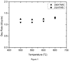
- Film densities for silicon oxides deposited from DMATMS ranged from 2.08 to 2.23 g/cm 3 .
- Figure 3 depicts the leakage current and breakdown comparison between thermal oxide and SiO 2 deposited with DMATMS at 650°C, demonstrating that silicon oxide using DMATMS has electrical properties comparable to thermal oxide.
- Steps 2a and 2b were repeated to introduce multiple doses of silicon precursor. Both deposition rate and non-uniformity are reported in Table IV. TABLE IV. Deposition Rates and Film Non-Uniformities of SiO 2 films deposited with multiple DMATMS doses Wafer temperature (Celcius) DMATMS dose (seconds) Deposition Rate ( ⁇ /cycle) Non-uniformity (%) 650 2 1.17 2.0 650 2+2 1.30 1.3 650 2+2+2 1.36 1.2
- the deposition rates show self-limiting behavior and saturates with increasing precursor doses which confirms ALD mode deposition at 650°C.
- Steps 2a and 2b are repeated to simulate multiple doses of silicon precursor. Both deposition rate and non-uniformity are reported in Table VII. TABLE VII. Deposition Rate and Film Non-Uniformity of SiO 2 films deposited with multiple DEATMS dose Wafer temperature (Celcius) Precursor dose (seconds) Deposition Rate ( ⁇ /cycle) Non-uniformity (%) 650 2 1.01 2.3 650 2+2 1.20 2.8 650 2+2+2 1.30 2.5 650 2+2+2+2 1.35 2.5
- the deposition rates show self-limiting behavior and saturates with increasing precursor doses which confirms ALD mode deposition at 650°C.
- Example 3 Atomic Layer Deposition of Silicon Oxide Films on a Patterned Silicon Substrate with DMATMS
- SiO 2 film was deposited on patterned silicon wafers with DMATMS. The deposition process was performed using ozone as the oxygen source gas and precursor double pulse of 8 seconds at 650°C. The film deposited on the substrate was measured using field emission scanning electron microscopy (FESEM) Hitachi S-4800 SEM. The samples were mounted in cross-sectional holders and examined using SEM operated at 2 kV accelerating voltage. SiO 2 thickness measurements of sample cross-sections were taken at the top, the side wall, and the bottom of the trench. A review of the SEM cross-section of the SiO 2 film indicated excellent step coverage (>96%) and confirmed that the process is indeed an ALD process.
- FESEM field emission scanning electron microscopy
- Example 4 Atomic Layer Deposition of Silicon Oxide Films with Diethylaminotriethylsilane (DEATES)
- Deposition of silicon oxide films were conducted using the silicon precursor diethylaminotriethylsilane (DEATES) and ozone. The deposition steps used are listed in Table I of Example 1.
- Table VIII summarizes deposition rates and non-uniformities of SiO 2 films deposited at wafer temperatures of 500 to 650°C using DEATES. TABLE VIII. Deposition Rates and Film Non-Uniformities of SiO 2 Films Deposited with Fixed DEATES Dose Wafer temperature (Celcius) Deposition Rate ( ⁇ /cycle) Non-uniformity (%) 500 0.91 1.44 550 0.97 1.1 600 1.18 7.8 650 2.53 24.8
- Atomic layers depositions of silicon oxide films were conducted using the silicon precursor methoxytrimethylsilane. Depositions were performed using ozone at 650°C with process steps listed in Table I of Example 1. The substrate temperature was set at 650°C. The deposition rate was about 0.3 ⁇ /cycle.
- Atomic layers deposition of silicon oxide films was conducted using the silicon precursor chlorotrimethylsilane. Depositions were performed using ozone as the oxygen source gas and the process parameters of the depositions are the same in Table I of Example 1.
- the substrate temperature was set at 650°C.
- the deposition rate was 0.5 ⁇ /cycle.
- Atomic layers depositions of silicon oxide films were conducted using the silicon precursor hexamethyldisilazane. Depositions were performed using ozone at 650°C with process steps listed in Table I of Example 1. The deposition rate was about 1.3 ⁇ /cycle.
- Example 8 (not in accordance with the invention) ALD Deposition of Silicon Oxide Film Using Bis(dimethylamino)dimethylsilane
- BDMADMS Bisdimethylaminodimethylsilane
- Depositions were performed on a laboratory scale ALD processing tool. Depositions were performed using ozone as the oxygen source gas and the process parameters of the depositions are the same in Table I.
- Deposition rates and film non-uniformities of silicon oxide films deposited using BDMADMS with fixed precursor dose (8 seconds) at 500-650°C are summarized in Table IX: TABLE IX.
- Deposition Rate and Film Non-Uniformity of SiO 2 films deposited with fixed BDMADMS dose Wafer temperature (Celcius) Deposition Rate ( ⁇ /cycle) Non-uniformity (%) 300 0.67 2.1 500 0.96 2.1 650 1.72 5.0
- Double precursor pulses process was used to further verify ALD mode.
- Table X shows the deposition rate and non-uniformity of the films with single 8 sec pulse and double 8 second pulses. TABLE X. Summary of Process Parameters and Results for BDMADMS Wafer temperature (Celcius) Precursor Pulse (seconds) Deposition Rate ( ⁇ /cycle) Non-uniformity (%) 650 8 1.72 5.0 650 8+8 2.05 7.8
Landscapes
- Chemical & Material Sciences (AREA)
- Engineering & Computer Science (AREA)
- Organic Chemistry (AREA)
- Chemical Kinetics & Catalysis (AREA)
- General Chemical & Material Sciences (AREA)
- Materials Engineering (AREA)
- Mechanical Engineering (AREA)
- Metallurgy (AREA)
- Physics & Mathematics (AREA)
- General Physics & Mathematics (AREA)
- Condensed Matter Physics & Semiconductors (AREA)
- Manufacturing & Machinery (AREA)
- Computer Hardware Design (AREA)
- Microelectronics & Electronic Packaging (AREA)
- Power Engineering (AREA)
- Inorganic Chemistry (AREA)
- Plasma & Fusion (AREA)
- Chemical Vapour Deposition (AREA)
- Formation Of Insulating Films (AREA)
Applications Claiming Priority (2)
| Application Number | Priority Date | Filing Date | Title |
|---|---|---|---|
| US201261623217P | 2012-04-12 | 2012-04-12 | |
| US13/857,507 US9460912B2 (en) | 2012-04-12 | 2013-04-05 | High temperature atomic layer deposition of silicon oxide thin films |
Publications (3)
| Publication Number | Publication Date |
|---|---|
| EP2650399A2 EP2650399A2 (en) | 2013-10-16 |
| EP2650399A3 EP2650399A3 (en) | 2013-10-30 |
| EP2650399B1 true EP2650399B1 (en) | 2019-09-11 |
Family
ID=48182719
Family Applications (1)
| Application Number | Title | Priority Date | Filing Date |
|---|---|---|---|
| EP13163586.4A Active EP2650399B1 (en) | 2012-04-12 | 2013-04-12 | High temperature atomic layer deposition of silicon oxide thin films |
Country Status (6)
| Country | Link |
|---|---|
| US (3) | US9460912B2 (ja) |
| EP (1) | EP2650399B1 (ja) |
| JP (5) | JP2013236073A (ja) |
| KR (5) | KR20130116210A (ja) |
| CN (1) | CN103374708B (ja) |
| TW (1) | TWI515325B (ja) |
Families Citing this family (357)
| Publication number | Priority date | Publication date | Assignee | Title |
|---|---|---|---|---|
| US10378106B2 (en) | 2008-11-14 | 2019-08-13 | Asm Ip Holding B.V. | Method of forming insulation film by modified PEALD |
| US9394608B2 (en) | 2009-04-06 | 2016-07-19 | Asm America, Inc. | Semiconductor processing reactor and components thereof |
| US8802201B2 (en) | 2009-08-14 | 2014-08-12 | Asm America, Inc. | Systems and methods for thin-film deposition of metal oxides using excited nitrogen-oxygen species |
| US9312155B2 (en) | 2011-06-06 | 2016-04-12 | Asm Japan K.K. | High-throughput semiconductor-processing apparatus equipped with multiple dual-chamber modules |
| US9793148B2 (en) | 2011-06-22 | 2017-10-17 | Asm Japan K.K. | Method for positioning wafers in multiple wafer transport |
| US10364496B2 (en) | 2011-06-27 | 2019-07-30 | Asm Ip Holding B.V. | Dual section module having shared and unshared mass flow controllers |
| US10854498B2 (en) | 2011-07-15 | 2020-12-01 | Asm Ip Holding B.V. | Wafer-supporting device and method for producing same |
| US20130023129A1 (en) | 2011-07-20 | 2013-01-24 | Asm America, Inc. | Pressure transmitter for a semiconductor processing environment |
| US9017481B1 (en) | 2011-10-28 | 2015-04-28 | Asm America, Inc. | Process feed management for semiconductor substrate processing |
| US9460912B2 (en) * | 2012-04-12 | 2016-10-04 | Air Products And Chemicals, Inc. | High temperature atomic layer deposition of silicon oxide thin films |
| US9659799B2 (en) | 2012-08-28 | 2017-05-23 | Asm Ip Holding B.V. | Systems and methods for dynamic semiconductor process scheduling |
| US10714315B2 (en) | 2012-10-12 | 2020-07-14 | Asm Ip Holdings B.V. | Semiconductor reaction chamber showerhead |
| US9640416B2 (en) | 2012-12-26 | 2017-05-02 | Asm Ip Holding B.V. | Single-and dual-chamber module-attachable wafer-handling chamber |
| US20160376700A1 (en) | 2013-02-01 | 2016-12-29 | Asm Ip Holding B.V. | System for treatment of deposition reactor |
| US9484191B2 (en) | 2013-03-08 | 2016-11-01 | Asm Ip Holding B.V. | Pulsed remote plasma method and system |
| US9589770B2 (en) | 2013-03-08 | 2017-03-07 | Asm Ip Holding B.V. | Method and systems for in-situ formation of intermediate reactive species |
| US9240412B2 (en) | 2013-09-27 | 2016-01-19 | Asm Ip Holding B.V. | Semiconductor structure and device and methods of forming same using selective epitaxial process |
| US9556516B2 (en) | 2013-10-09 | 2017-01-31 | ASM IP Holding B.V | Method for forming Ti-containing film by PEALD using TDMAT or TDEAT |
| US10179947B2 (en) | 2013-11-26 | 2019-01-15 | Asm Ip Holding B.V. | Method for forming conformal nitrided, oxidized, or carbonized dielectric film by atomic layer deposition |
| KR101720017B1 (ko) * | 2014-01-08 | 2017-03-27 | (주)디엔에프 | 신규한 트리실릴아민 유도체, 이의 제조방법 및 이를 이용한 실리콘 함유 박막 |
| US10683571B2 (en) | 2014-02-25 | 2020-06-16 | Asm Ip Holding B.V. | Gas supply manifold and method of supplying gases to chamber using same |
| US10167557B2 (en) | 2014-03-18 | 2019-01-01 | Asm Ip Holding B.V. | Gas distribution system, reactor including the system, and methods of using the same |
| US9447498B2 (en) | 2014-03-18 | 2016-09-20 | Asm Ip Holding B.V. | Method for performing uniform processing in gas system-sharing multiple reaction chambers |
| US11015245B2 (en) | 2014-03-19 | 2021-05-25 | Asm Ip Holding B.V. | Gas-phase reactor and system having exhaust plenum and components thereof |
| US9583337B2 (en) | 2014-03-26 | 2017-02-28 | Ultratech, Inc. | Oxygen radical enhanced atomic-layer deposition using ozone plasma |
| US20150275355A1 (en) | 2014-03-26 | 2015-10-01 | Air Products And Chemicals, Inc. | Compositions and methods for the deposition of silicon oxide films |
| CN105097500B (zh) * | 2014-05-23 | 2020-02-11 | 中芯国际集成电路制造(上海)有限公司 | 一种半导体器件及其制造方法、电子装置 |
| US10113234B2 (en) * | 2014-07-21 | 2018-10-30 | Applied Materials, Inc. | UV assisted silylation for porous low-k film sealing |
| CN104120404A (zh) * | 2014-07-23 | 2014-10-29 | 国家纳米科学中心 | 一种超薄氧化硅膜材料及其制备方法 |
| CN104099581A (zh) * | 2014-07-23 | 2014-10-15 | 国家纳米科学中心 | 一种氧化硅膜材料及其制备方法 |
| US10858737B2 (en) | 2014-07-28 | 2020-12-08 | Asm Ip Holding B.V. | Showerhead assembly and components thereof |
| US9543180B2 (en) | 2014-08-01 | 2017-01-10 | Asm Ip Holding B.V. | Apparatus and method for transporting wafers between wafer carrier and process tool under vacuum |
| US9890456B2 (en) | 2014-08-21 | 2018-02-13 | Asm Ip Holding B.V. | Method and system for in situ formation of gas-phase compounds |
| US9478414B2 (en) | 2014-09-26 | 2016-10-25 | Asm Ip Holding B.V. | Method for hydrophobization of surface of silicon-containing film by ALD |
| US9875888B2 (en) * | 2014-10-03 | 2018-01-23 | Applied Materials, Inc. | High temperature silicon oxide atomic layer deposition technology |
| US10941490B2 (en) | 2014-10-07 | 2021-03-09 | Asm Ip Holding B.V. | Multiple temperature range susceptor, assembly, reactor and system including the susceptor, and methods of using the same |
| US9657845B2 (en) | 2014-10-07 | 2017-05-23 | Asm Ip Holding B.V. | Variable conductance gas distribution apparatus and method |
| KR102263121B1 (ko) | 2014-12-22 | 2021-06-09 | 에이에스엠 아이피 홀딩 비.브이. | 반도체 소자 및 그 제조 방법 |
| US9478415B2 (en) | 2015-02-13 | 2016-10-25 | Asm Ip Holding B.V. | Method for forming film having low resistance and shallow junction depth |
| US10529542B2 (en) | 2015-03-11 | 2020-01-07 | Asm Ip Holdings B.V. | Cross-flow reactor and method |
| US10276355B2 (en) | 2015-03-12 | 2019-04-30 | Asm Ip Holding B.V. | Multi-zone reactor, system including the reactor, and method of using the same |
| CN104911561B (zh) * | 2015-04-14 | 2017-12-26 | 中国计量科学研究院 | 制备高厚度均匀性纳米/亚微米SiO2薄膜的方法 |
| US10458018B2 (en) | 2015-06-26 | 2019-10-29 | Asm Ip Holding B.V. | Structures including metal carbide material, devices including the structures, and methods of forming same |
| US10600673B2 (en) | 2015-07-07 | 2020-03-24 | Asm Ip Holding B.V. | Magnetic susceptor to baseplate seal |
| US9899291B2 (en) | 2015-07-13 | 2018-02-20 | Asm Ip Holding B.V. | Method for protecting layer by forming hydrocarbon-based extremely thin film |
| US9711345B2 (en) | 2015-08-25 | 2017-07-18 | Asm Ip Holding B.V. | Method for forming aluminum nitride-based film by PEALD |
| EP3347504A1 (en) * | 2015-09-11 | 2018-07-18 | Air Products and Chemicals, Inc. | Methods for depositing a conformal metal or metalloid silicon nitride film and resultant films |
| US9960072B2 (en) | 2015-09-29 | 2018-05-01 | Asm Ip Holding B.V. | Variable adjustment for precise matching of multiple chamber cavity housings |
| US9909214B2 (en) | 2015-10-15 | 2018-03-06 | Asm Ip Holding B.V. | Method for depositing dielectric film in trenches by PEALD |
| US10211308B2 (en) | 2015-10-21 | 2019-02-19 | Asm Ip Holding B.V. | NbMC layers |
| US10322384B2 (en) | 2015-11-09 | 2019-06-18 | Asm Ip Holding B.V. | Counter flow mixer for process chamber |
| US9455138B1 (en) | 2015-11-10 | 2016-09-27 | Asm Ip Holding B.V. | Method for forming dielectric film in trenches by PEALD using H-containing gas |
| US9607837B1 (en) | 2015-12-21 | 2017-03-28 | Asm Ip Holding B.V. | Method for forming silicon oxide cap layer for solid state diffusion process |
| US9735024B2 (en) | 2015-12-28 | 2017-08-15 | Asm Ip Holding B.V. | Method of atomic layer etching using functional group-containing fluorocarbon |
| US9633838B2 (en) * | 2015-12-28 | 2017-04-25 | L'Air Liquide, Société Anonyme pour l'Etude et l'Exploitation des Procédés Georges Claude | Vapor deposition of silicon-containing films using penta-substituted disilanes |
| US9627221B1 (en) | 2015-12-28 | 2017-04-18 | Asm Ip Holding B.V. | Continuous process incorporating atomic layer etching |
| US11139308B2 (en) | 2015-12-29 | 2021-10-05 | Asm Ip Holding B.V. | Atomic layer deposition of III-V compounds to form V-NAND devices |
| US10283348B2 (en) * | 2016-01-20 | 2019-05-07 | Versum Materials Us, Llc | High temperature atomic layer deposition of silicon-containing films |
| US10529554B2 (en) | 2016-02-19 | 2020-01-07 | Asm Ip Holding B.V. | Method for forming silicon nitride film selectively on sidewalls or flat surfaces of trenches |
| US10468251B2 (en) | 2016-02-19 | 2019-11-05 | Asm Ip Holding B.V. | Method for forming spacers using silicon nitride film for spacer-defined multiple patterning |
| US9754779B1 (en) | 2016-02-19 | 2017-09-05 | Asm Ip Holding B.V. | Method for forming silicon nitride film selectively on sidewalls or flat surfaces of trenches |
| US10501866B2 (en) | 2016-03-09 | 2019-12-10 | Asm Ip Holding B.V. | Gas distribution apparatus for improved film uniformity in an epitaxial system |
| US10343920B2 (en) | 2016-03-18 | 2019-07-09 | Asm Ip Holding B.V. | Aligned carbon nanotubes |
| US9892913B2 (en) | 2016-03-24 | 2018-02-13 | Asm Ip Holding B.V. | Radial and thickness control via biased multi-port injection settings |
| CN105870249B (zh) * | 2016-03-24 | 2017-10-03 | 江苏微导纳米装备科技有限公司 | 一种晶硅太阳能电池的制造工艺 |
| US10190213B2 (en) | 2016-04-21 | 2019-01-29 | Asm Ip Holding B.V. | Deposition of metal borides |
| US10865475B2 (en) | 2016-04-21 | 2020-12-15 | Asm Ip Holding B.V. | Deposition of metal borides and silicides |
| US10367080B2 (en) | 2016-05-02 | 2019-07-30 | Asm Ip Holding B.V. | Method of forming a germanium oxynitride film |
| US10032628B2 (en) | 2016-05-02 | 2018-07-24 | Asm Ip Holding B.V. | Source/drain performance through conformal solid state doping |
| KR102592471B1 (ko) | 2016-05-17 | 2023-10-20 | 에이에스엠 아이피 홀딩 비.브이. | 금속 배선 형성 방법 및 이를 이용한 반도체 장치의 제조 방법 |
| US11453943B2 (en) | 2016-05-25 | 2022-09-27 | Asm Ip Holding B.V. | Method for forming carbon-containing silicon/metal oxide or nitride film by ALD using silicon precursor and hydrocarbon precursor |
| US10388509B2 (en) | 2016-06-28 | 2019-08-20 | Asm Ip Holding B.V. | Formation of epitaxial layers via dislocation filtering |
| US10612137B2 (en) | 2016-07-08 | 2020-04-07 | Asm Ip Holdings B.V. | Organic reactants for atomic layer deposition |
| US9859151B1 (en) | 2016-07-08 | 2018-01-02 | Asm Ip Holding B.V. | Selective film deposition method to form air gaps |
| US10714385B2 (en) | 2016-07-19 | 2020-07-14 | Asm Ip Holding B.V. | Selective deposition of tungsten |
| KR102354490B1 (ko) | 2016-07-27 | 2022-01-21 | 에이에스엠 아이피 홀딩 비.브이. | 기판 처리 방법 |
| KR102532607B1 (ko) | 2016-07-28 | 2023-05-15 | 에이에스엠 아이피 홀딩 비.브이. | 기판 가공 장치 및 그 동작 방법 |
| US9887082B1 (en) | 2016-07-28 | 2018-02-06 | Asm Ip Holding B.V. | Method and apparatus for filling a gap |
| US10395919B2 (en) | 2016-07-28 | 2019-08-27 | Asm Ip Holding B.V. | Method and apparatus for filling a gap |
| US9812320B1 (en) | 2016-07-28 | 2017-11-07 | Asm Ip Holding B.V. | Method and apparatus for filling a gap |
| KR102613349B1 (ko) | 2016-08-25 | 2023-12-14 | 에이에스엠 아이피 홀딩 비.브이. | 배기 장치 및 이를 이용한 기판 가공 장치와 박막 제조 방법 |
| US10703915B2 (en) * | 2016-09-19 | 2020-07-07 | Versum Materials Us, Llc | Compositions and methods for the deposition of silicon oxide films |
| US10410943B2 (en) | 2016-10-13 | 2019-09-10 | Asm Ip Holding B.V. | Method for passivating a surface of a semiconductor and related systems |
| US10464953B2 (en) | 2016-10-14 | 2019-11-05 | Versum Materials Us, Llc | Carbon bridged aminosilane compounds for high growth rate silicon-containing films |
| US10643826B2 (en) | 2016-10-26 | 2020-05-05 | Asm Ip Holdings B.V. | Methods for thermally calibrating reaction chambers |
| US11532757B2 (en) | 2016-10-27 | 2022-12-20 | Asm Ip Holding B.V. | Deposition of charge trapping layers |
| US10435790B2 (en) | 2016-11-01 | 2019-10-08 | Asm Ip Holding B.V. | Method of subatmospheric plasma-enhanced ALD using capacitively coupled electrodes with narrow gap |
| US10229833B2 (en) | 2016-11-01 | 2019-03-12 | Asm Ip Holding B.V. | Methods for forming a transition metal nitride film on a substrate by atomic layer deposition and related semiconductor device structures |
| US10714350B2 (en) | 2016-11-01 | 2020-07-14 | ASM IP Holdings, B.V. | Methods for forming a transition metal niobium nitride film on a substrate by atomic layer deposition and related semiconductor device structures |
| US10643904B2 (en) | 2016-11-01 | 2020-05-05 | Asm Ip Holdings B.V. | Methods for forming a semiconductor device and related semiconductor device structures |
| US10134757B2 (en) | 2016-11-07 | 2018-11-20 | Asm Ip Holding B.V. | Method of processing a substrate and a device manufactured by using the method |
| KR102546317B1 (ko) | 2016-11-15 | 2023-06-21 | 에이에스엠 아이피 홀딩 비.브이. | 기체 공급 유닛 및 이를 포함하는 기판 처리 장치 |
| US10340135B2 (en) | 2016-11-28 | 2019-07-02 | Asm Ip Holding B.V. | Method of topologically restricted plasma-enhanced cyclic deposition of silicon or metal nitride |
| KR20180068582A (ko) | 2016-12-14 | 2018-06-22 | 에이에스엠 아이피 홀딩 비.브이. | 기판 처리 장치 |
| US11447861B2 (en) | 2016-12-15 | 2022-09-20 | Asm Ip Holding B.V. | Sequential infiltration synthesis apparatus and a method of forming a patterned structure |
| US11581186B2 (en) | 2016-12-15 | 2023-02-14 | Asm Ip Holding B.V. | Sequential infiltration synthesis apparatus |
| KR20180070971A (ko) | 2016-12-19 | 2018-06-27 | 에이에스엠 아이피 홀딩 비.브이. | 기판 처리 장치 |
| US10269558B2 (en) | 2016-12-22 | 2019-04-23 | Asm Ip Holding B.V. | Method of forming a structure on a substrate |
| US10867788B2 (en) | 2016-12-28 | 2020-12-15 | Asm Ip Holding B.V. | Method of forming a structure on a substrate |
| US11390950B2 (en) | 2017-01-10 | 2022-07-19 | Asm Ip Holding B.V. | Reactor system and method to reduce residue buildup during a film deposition process |
| US10655221B2 (en) | 2017-02-09 | 2020-05-19 | Asm Ip Holding B.V. | Method for depositing oxide film by thermal ALD and PEALD |
| US10468261B2 (en) | 2017-02-15 | 2019-11-05 | Asm Ip Holding B.V. | Methods for forming a metallic film on a substrate by cyclical deposition and related semiconductor device structures |
| US11631580B2 (en) | 2017-03-15 | 2023-04-18 | Versum Materials Us, Llc | Formulation for deposition of silicon doped hafnium oxide as ferroelectric materials |
| US11081337B2 (en) * | 2017-03-15 | 2021-08-03 | Versum Materials U.S., LLC | Formulation for deposition of silicon doped hafnium oxide as ferroelectric materials |
| US11193206B2 (en) * | 2017-03-15 | 2021-12-07 | Versum Materials Us, Llc | Formulation for deposition of silicon doped hafnium oxide as ferroelectric materials |
| US10529563B2 (en) | 2017-03-29 | 2020-01-07 | Asm Ip Holdings B.V. | Method for forming doped metal oxide films on a substrate by cyclical deposition and related semiconductor device structures |
| US10283353B2 (en) | 2017-03-29 | 2019-05-07 | Asm Ip Holding B.V. | Method of reforming insulating film deposited on substrate with recess pattern |
| KR102548405B1 (ko) | 2017-04-20 | 2023-06-28 | (주)디엔에프 | 다이실릴아민 화합물을 포함하는 실리콘 함유 박막증착용 조성물 및 이를 이용하는 실리콘 함유 박막의 제조방법 |
| KR102093227B1 (ko) | 2017-04-20 | 2020-03-25 | (주)디엔에프 | 다이실릴아민 화합물, 이의 제조방법 및 이를 포함하는 실리콘 함유 박막증착용 조성물 |
| KR102457289B1 (ko) | 2017-04-25 | 2022-10-21 | 에이에스엠 아이피 홀딩 비.브이. | 박막 증착 방법 및 반도체 장치의 제조 방법 |
| US10446393B2 (en) | 2017-05-08 | 2019-10-15 | Asm Ip Holding B.V. | Methods for forming silicon-containing epitaxial layers and related semiconductor device structures |
| US10892156B2 (en) | 2017-05-08 | 2021-01-12 | Asm Ip Holding B.V. | Methods for forming a silicon nitride film on a substrate and related semiconductor device structures |
| US10770286B2 (en) | 2017-05-08 | 2020-09-08 | Asm Ip Holdings B.V. | Methods for selectively forming a silicon nitride film on a substrate and related semiconductor device structures |
| US11177127B2 (en) * | 2017-05-24 | 2021-11-16 | Versum Materials Us, Llc | Functionalized cyclosilazanes as precursors for high growth rate silicon-containing films |
| US10504742B2 (en) | 2017-05-31 | 2019-12-10 | Asm Ip Holding B.V. | Method of atomic layer etching using hydrogen plasma |
| US10886123B2 (en) | 2017-06-02 | 2021-01-05 | Asm Ip Holding B.V. | Methods for forming low temperature semiconductor layers and related semiconductor device structures |
| US11306395B2 (en) | 2017-06-28 | 2022-04-19 | Asm Ip Holding B.V. | Methods for depositing a transition metal nitride film on a substrate by atomic layer deposition and related deposition apparatus |
| US10685834B2 (en) | 2017-07-05 | 2020-06-16 | Asm Ip Holdings B.V. | Methods for forming a silicon germanium tin layer and related semiconductor device structures |
| KR20190009245A (ko) | 2017-07-18 | 2019-01-28 | 에이에스엠 아이피 홀딩 비.브이. | 반도체 소자 구조물 형성 방법 및 관련된 반도체 소자 구조물 |
| US10541333B2 (en) | 2017-07-19 | 2020-01-21 | Asm Ip Holding B.V. | Method for depositing a group IV semiconductor and related semiconductor device structures |
| US11018002B2 (en) | 2017-07-19 | 2021-05-25 | Asm Ip Holding B.V. | Method for selectively depositing a Group IV semiconductor and related semiconductor device structures |
| US11374112B2 (en) | 2017-07-19 | 2022-06-28 | Asm Ip Holding B.V. | Method for depositing a group IV semiconductor and related semiconductor device structures |
| US10590535B2 (en) | 2017-07-26 | 2020-03-17 | Asm Ip Holdings B.V. | Chemical treatment, deposition and/or infiltration apparatus and method for using the same |
| US10605530B2 (en) | 2017-07-26 | 2020-03-31 | Asm Ip Holding B.V. | Assembly of a liner and a flange for a vertical furnace as well as the liner and the vertical furnace |
| US10312055B2 (en) | 2017-07-26 | 2019-06-04 | Asm Ip Holding B.V. | Method of depositing film by PEALD using negative bias |
| US10692741B2 (en) | 2017-08-08 | 2020-06-23 | Asm Ip Holdings B.V. | Radiation shield |
| US10770336B2 (en) | 2017-08-08 | 2020-09-08 | Asm Ip Holding B.V. | Substrate lift mechanism and reactor including same |
| US11769682B2 (en) | 2017-08-09 | 2023-09-26 | Asm Ip Holding B.V. | Storage apparatus for storing cassettes for substrates and processing apparatus equipped therewith |
| US11139191B2 (en) | 2017-08-09 | 2021-10-05 | Asm Ip Holding B.V. | Storage apparatus for storing cassettes for substrates and processing apparatus equipped therewith |
| US10249524B2 (en) | 2017-08-09 | 2019-04-02 | Asm Ip Holding B.V. | Cassette holder assembly for a substrate cassette and holding member for use in such assembly |
| JP6676592B2 (ja) * | 2017-08-22 | 2020-04-08 | キヤノン株式会社 | 液体吐出ヘッドの製造方法 |
| CN107523809B (zh) * | 2017-08-23 | 2019-06-25 | 江苏菲沃泰纳米科技有限公司 | 一种有机硅硬质纳米防护涂层的制备方法 |
| USD900036S1 (en) | 2017-08-24 | 2020-10-27 | Asm Ip Holding B.V. | Heater electrical connector and adapter |
| US11830730B2 (en) | 2017-08-29 | 2023-11-28 | Asm Ip Holding B.V. | Layer forming method and apparatus |
| KR102491945B1 (ko) | 2017-08-30 | 2023-01-26 | 에이에스엠 아이피 홀딩 비.브이. | 기판 처리 장치 |
| US11295980B2 (en) | 2017-08-30 | 2022-04-05 | Asm Ip Holding B.V. | Methods for depositing a molybdenum metal film over a dielectric surface of a substrate by a cyclical deposition process and related semiconductor device structures |
| US11056344B2 (en) | 2017-08-30 | 2021-07-06 | Asm Ip Holding B.V. | Layer forming method |
| US10607895B2 (en) | 2017-09-18 | 2020-03-31 | Asm Ip Holdings B.V. | Method for forming a semiconductor device structure comprising a gate fill metal |
| US11049714B2 (en) * | 2017-09-19 | 2021-06-29 | Versum Materials Us, Llc | Silyl substituted organoamines as precursors for high growth rate silicon-containing films |
| KR102630301B1 (ko) | 2017-09-21 | 2024-01-29 | 에이에스엠 아이피 홀딩 비.브이. | 침투성 재료의 순차 침투 합성 방법 처리 및 이를 이용하여 형성된 구조물 및 장치 |
| US10844484B2 (en) | 2017-09-22 | 2020-11-24 | Asm Ip Holding B.V. | Apparatus for dispensing a vapor phase reactant to a reaction chamber and related methods |
| US10658205B2 (en) | 2017-09-28 | 2020-05-19 | Asm Ip Holdings B.V. | Chemical dispensing apparatus and methods for dispensing a chemical to a reaction chamber |
| US10403504B2 (en) | 2017-10-05 | 2019-09-03 | Asm Ip Holding B.V. | Method for selectively depositing a metallic film on a substrate |
| US10319588B2 (en) | 2017-10-10 | 2019-06-11 | Asm Ip Holding B.V. | Method for depositing a metal chalcogenide on a substrate by cyclical deposition |
| KR102251040B1 (ko) | 2017-10-24 | 2021-05-12 | (주)덕산테코피아 | 아미노실란 전구체 화합물 및 이를 사용하는 박막 형성 방법 |
| US10923344B2 (en) | 2017-10-30 | 2021-02-16 | Asm Ip Holding B.V. | Methods for forming a semiconductor structure and related semiconductor structures |
| US10910262B2 (en) | 2017-11-16 | 2021-02-02 | Asm Ip Holding B.V. | Method of selectively depositing a capping layer structure on a semiconductor device structure |
| KR102443047B1 (ko) | 2017-11-16 | 2022-09-14 | 에이에스엠 아이피 홀딩 비.브이. | 기판 처리 장치 방법 및 그에 의해 제조된 장치 |
| US11022879B2 (en) | 2017-11-24 | 2021-06-01 | Asm Ip Holding B.V. | Method of forming an enhanced unexposed photoresist layer |
| US11639811B2 (en) | 2017-11-27 | 2023-05-02 | Asm Ip Holding B.V. | Apparatus including a clean mini environment |
| KR102597978B1 (ko) | 2017-11-27 | 2023-11-06 | 에이에스엠 아이피 홀딩 비.브이. | 배치 퍼니스와 함께 사용하기 위한 웨이퍼 카세트를 보관하기 위한 보관 장치 |
| US10290508B1 (en) | 2017-12-05 | 2019-05-14 | Asm Ip Holding B.V. | Method for forming vertical spacers for spacer-defined patterning |
| US10872771B2 (en) | 2018-01-16 | 2020-12-22 | Asm Ip Holding B. V. | Method for depositing a material film on a substrate within a reaction chamber by a cyclical deposition process and related device structures |
| US11482412B2 (en) | 2018-01-19 | 2022-10-25 | Asm Ip Holding B.V. | Method for depositing a gap-fill layer by plasma-assisted deposition |
| TW202325889A (zh) | 2018-01-19 | 2023-07-01 | 荷蘭商Asm 智慧財產控股公司 | 沈積方法 |
| USD903477S1 (en) | 2018-01-24 | 2020-12-01 | Asm Ip Holdings B.V. | Metal clamp |
| US11018047B2 (en) | 2018-01-25 | 2021-05-25 | Asm Ip Holding B.V. | Hybrid lift pin |
| USD880437S1 (en) | 2018-02-01 | 2020-04-07 | Asm Ip Holding B.V. | Gas supply plate for semiconductor manufacturing apparatus |
| US10535516B2 (en) | 2018-02-01 | 2020-01-14 | Asm Ip Holdings B.V. | Method for depositing a semiconductor structure on a surface of a substrate and related semiconductor structures |
| US11081345B2 (en) | 2018-02-06 | 2021-08-03 | Asm Ip Holding B.V. | Method of post-deposition treatment for silicon oxide film |
| WO2019158960A1 (en) | 2018-02-14 | 2019-08-22 | Asm Ip Holding B.V. | A method for depositing a ruthenium-containing film on a substrate by a cyclical deposition process |
| US10896820B2 (en) | 2018-02-14 | 2021-01-19 | Asm Ip Holding B.V. | Method for depositing a ruthenium-containing film on a substrate by a cyclical deposition process |
| US10731249B2 (en) | 2018-02-15 | 2020-08-04 | Asm Ip Holding B.V. | Method of forming a transition metal containing film on a substrate by a cyclical deposition process, a method for supplying a transition metal halide compound to a reaction chamber, and related vapor deposition apparatus |
| KR102636427B1 (ko) | 2018-02-20 | 2024-02-13 | 에이에스엠 아이피 홀딩 비.브이. | 기판 처리 방법 및 장치 |
| US10658181B2 (en) | 2018-02-20 | 2020-05-19 | Asm Ip Holding B.V. | Method of spacer-defined direct patterning in semiconductor fabrication |
| US10975470B2 (en) | 2018-02-23 | 2021-04-13 | Asm Ip Holding B.V. | Apparatus for detecting or monitoring for a chemical precursor in a high temperature environment |
| US11473195B2 (en) | 2018-03-01 | 2022-10-18 | Asm Ip Holding B.V. | Semiconductor processing apparatus and a method for processing a substrate |
| KR20190105970A (ko) | 2018-03-07 | 2019-09-18 | (주)덕산테코피아 | SiC 전구체 화합물 및 이를 사용하는 박막 형성 방법 |
| US11629406B2 (en) | 2018-03-09 | 2023-04-18 | Asm Ip Holding B.V. | Semiconductor processing apparatus comprising one or more pyrometers for measuring a temperature of a substrate during transfer of the substrate |
| US11114283B2 (en) | 2018-03-16 | 2021-09-07 | Asm Ip Holding B.V. | Reactor, system including the reactor, and methods of manufacturing and using same |
| KR102646467B1 (ko) | 2018-03-27 | 2024-03-11 | 에이에스엠 아이피 홀딩 비.브이. | 기판 상에 전극을 형성하는 방법 및 전극을 포함하는 반도체 소자 구조 |
| US11230766B2 (en) | 2018-03-29 | 2022-01-25 | Asm Ip Holding B.V. | Substrate processing apparatus and method |
| US10510536B2 (en) | 2018-03-29 | 2019-12-17 | Asm Ip Holding B.V. | Method of depositing a co-doped polysilicon film on a surface of a substrate within a reaction chamber |
| US11088002B2 (en) | 2018-03-29 | 2021-08-10 | Asm Ip Holding B.V. | Substrate rack and a substrate processing system and method |
| KR102173384B1 (ko) | 2018-03-30 | 2020-11-03 | 에스케이트리켐 주식회사 | SiO2 박막 형성용 전구체 및 이를 이용한 SiO2 박막 형성. |
| KR102501472B1 (ko) | 2018-03-30 | 2023-02-20 | 에이에스엠 아이피 홀딩 비.브이. | 기판 처리 방법 |
| US20210384029A1 (en) * | 2018-04-09 | 2021-12-09 | Lam Research Corporation | Modifying hydrophobicity of a wafer surface using an organosilicon precursor |
| TWI811348B (zh) | 2018-05-08 | 2023-08-11 | 荷蘭商Asm 智慧財產控股公司 | 藉由循環沉積製程於基板上沉積氧化物膜之方法及相關裝置結構 |
| TWI816783B (zh) | 2018-05-11 | 2023-10-01 | 荷蘭商Asm 智慧財產控股公司 | 用於基板上形成摻雜金屬碳化物薄膜之方法及相關半導體元件結構 |
| KR102596988B1 (ko) | 2018-05-28 | 2023-10-31 | 에이에스엠 아이피 홀딩 비.브이. | 기판 처리 방법 및 그에 의해 제조된 장치 |
| US11270899B2 (en) | 2018-06-04 | 2022-03-08 | Asm Ip Holding B.V. | Wafer handling chamber with moisture reduction |
| US11718913B2 (en) | 2018-06-04 | 2023-08-08 | Asm Ip Holding B.V. | Gas distribution system and reactor system including same |
| US11286562B2 (en) | 2018-06-08 | 2022-03-29 | Asm Ip Holding B.V. | Gas-phase chemical reactor and method of using same |
| KR102568797B1 (ko) | 2018-06-21 | 2023-08-21 | 에이에스엠 아이피 홀딩 비.브이. | 기판 처리 시스템 |
| US10797133B2 (en) | 2018-06-21 | 2020-10-06 | Asm Ip Holding B.V. | Method for depositing a phosphorus doped silicon arsenide film and related semiconductor device structures |
| JP2021529254A (ja) | 2018-06-27 | 2021-10-28 | エーエスエム・アイピー・ホールディング・ベー・フェー | 金属含有材料ならびに金属含有材料を含む膜および構造体を形成するための周期的堆積方法 |
| CN112292477A (zh) | 2018-06-27 | 2021-01-29 | Asm Ip私人控股有限公司 | 用于形成含金属的材料的循环沉积方法及包含含金属的材料的膜和结构 |
| US10612136B2 (en) | 2018-06-29 | 2020-04-07 | ASM IP Holding, B.V. | Temperature-controlled flange and reactor system including same |
| KR20200002519A (ko) | 2018-06-29 | 2020-01-08 | 에이에스엠 아이피 홀딩 비.브이. | 박막 증착 방법 및 반도체 장치의 제조 방법 |
| US10388513B1 (en) | 2018-07-03 | 2019-08-20 | Asm Ip Holding B.V. | Method for depositing silicon-free carbon-containing film as gap-fill layer by pulse plasma-assisted deposition |
| US10755922B2 (en) | 2018-07-03 | 2020-08-25 | Asm Ip Holding B.V. | Method for depositing silicon-free carbon-containing film as gap-fill layer by pulse plasma-assisted deposition |
| US10767789B2 (en) | 2018-07-16 | 2020-09-08 | Asm Ip Holding B.V. | Diaphragm valves, valve components, and methods for forming valve components |
| US10483099B1 (en) | 2018-07-26 | 2019-11-19 | Asm Ip Holding B.V. | Method for forming thermally stable organosilicon polymer film |
| US11053591B2 (en) | 2018-08-06 | 2021-07-06 | Asm Ip Holding B.V. | Multi-port gas injection system and reactor system including same |
| US10883175B2 (en) | 2018-08-09 | 2021-01-05 | Asm Ip Holding B.V. | Vertical furnace for processing substrates and a liner for use therein |
| US10829852B2 (en) | 2018-08-16 | 2020-11-10 | Asm Ip Holding B.V. | Gas distribution device for a wafer processing apparatus |
| US11430674B2 (en) | 2018-08-22 | 2022-08-30 | Asm Ip Holding B.V. | Sensor array, apparatus for dispensing a vapor phase reactant to a reaction chamber and related methods |
| US10985010B2 (en) * | 2018-08-29 | 2021-04-20 | Versum Materials Us, Llc | Methods for making silicon and nitrogen containing films |
| US11024523B2 (en) | 2018-09-11 | 2021-06-01 | Asm Ip Holding B.V. | Substrate processing apparatus and method |
| KR20200030162A (ko) | 2018-09-11 | 2020-03-20 | 에이에스엠 아이피 홀딩 비.브이. | 박막 증착 방법 |
| US11049751B2 (en) | 2018-09-14 | 2021-06-29 | Asm Ip Holding B.V. | Cassette supply system to store and handle cassettes and processing apparatus equipped therewith |
| US11567407B2 (en) * | 2018-09-28 | 2023-01-31 | Tokyo Electron Limited | Method for globally adjusting spacer critical dimension using photo-active self-assembled monolayer |
| CN110970344A (zh) | 2018-10-01 | 2020-04-07 | Asm Ip控股有限公司 | 衬底保持设备、包含所述设备的系统及其使用方法 |
| US11232963B2 (en) | 2018-10-03 | 2022-01-25 | Asm Ip Holding B.V. | Substrate processing apparatus and method |
| KR20210054035A (ko) * | 2018-10-04 | 2021-05-12 | 버슘머트리얼즈 유에스, 엘엘씨 | 고품질 실리콘 옥사이드 박막의 고온 원자 층 증착용 조성물 |
| US20210380418A1 (en) * | 2018-10-05 | 2021-12-09 | Versum Materials Us, Llc | High temperature atomic layer deposition of silicon-containing film |
| KR102592699B1 (ko) | 2018-10-08 | 2023-10-23 | 에이에스엠 아이피 홀딩 비.브이. | 기판 지지 유닛 및 이를 포함하는 박막 증착 장치와 기판 처리 장치 |
| US10847365B2 (en) | 2018-10-11 | 2020-11-24 | Asm Ip Holding B.V. | Method of forming conformal silicon carbide film by cyclic CVD |
| US10811256B2 (en) | 2018-10-16 | 2020-10-20 | Asm Ip Holding B.V. | Method for etching a carbon-containing feature |
| KR102546322B1 (ko) | 2018-10-19 | 2023-06-21 | 에이에스엠 아이피 홀딩 비.브이. | 기판 처리 장치 및 기판 처리 방법 |
| KR102605121B1 (ko) | 2018-10-19 | 2023-11-23 | 에이에스엠 아이피 홀딩 비.브이. | 기판 처리 장치 및 기판 처리 방법 |
| USD948463S1 (en) | 2018-10-24 | 2022-04-12 | Asm Ip Holding B.V. | Susceptor for semiconductor substrate supporting apparatus |
| US10381219B1 (en) | 2018-10-25 | 2019-08-13 | Asm Ip Holding B.V. | Methods for forming a silicon nitride film |
| JP7087917B2 (ja) | 2018-10-31 | 2022-06-21 | 住友ゴム工業株式会社 | クロスプライタイヤの製造方法 |
| US11087997B2 (en) | 2018-10-31 | 2021-08-10 | Asm Ip Holding B.V. | Substrate processing apparatus for processing substrates |
| KR20200051105A (ko) | 2018-11-02 | 2020-05-13 | 에이에스엠 아이피 홀딩 비.브이. | 기판 지지 유닛 및 이를 포함하는 기판 처리 장치 |
| US11572620B2 (en) | 2018-11-06 | 2023-02-07 | Asm Ip Holding B.V. | Methods for selectively depositing an amorphous silicon film on a substrate |
| US11031242B2 (en) | 2018-11-07 | 2021-06-08 | Asm Ip Holding B.V. | Methods for depositing a boron doped silicon germanium film |
| US10818758B2 (en) | 2018-11-16 | 2020-10-27 | Asm Ip Holding B.V. | Methods for forming a metal silicate film on a substrate in a reaction chamber and related semiconductor device structures |
| US10847366B2 (en) | 2018-11-16 | 2020-11-24 | Asm Ip Holding B.V. | Methods for depositing a transition metal chalcogenide film on a substrate by a cyclical deposition process |
| US10559458B1 (en) | 2018-11-26 | 2020-02-11 | Asm Ip Holding B.V. | Method of forming oxynitride film |
| US11217444B2 (en) | 2018-11-30 | 2022-01-04 | Asm Ip Holding B.V. | Method for forming an ultraviolet radiation responsive metal oxide-containing film |
| EP3680245A4 (en) * | 2018-11-30 | 2020-07-22 | Hansol Chemical Co., Ltd | SILICON PRECURSOR AND METHOD FOR PRODUCING A THIN FILM CONTAINING SILICON USING THEREOF |
| KR102157137B1 (ko) * | 2018-11-30 | 2020-09-17 | 주식회사 한솔케미칼 | 실리콘 전구체 및 이를 이용한 실리콘 함유 박막의 제조방법 |
| KR102636428B1 (ko) | 2018-12-04 | 2024-02-13 | 에이에스엠 아이피 홀딩 비.브이. | 기판 처리 장치를 세정하는 방법 |
| US11158513B2 (en) | 2018-12-13 | 2021-10-26 | Asm Ip Holding B.V. | Methods for forming a rhenium-containing film on a substrate by a cyclical deposition process and related semiconductor device structures |
| JP2020096183A (ja) | 2018-12-14 | 2020-06-18 | エーエスエム・アイピー・ホールディング・ベー・フェー | 窒化ガリウムの選択的堆積を用いてデバイス構造体を形成する方法及びそのためのシステム |
| KR20210104123A (ko) * | 2018-12-21 | 2021-08-24 | 레르 리키드 쏘시에떼 아노님 뿌르 레뜌드 에렉스뿔라따시옹 데 프로세데 조르즈 클로드 | 550℃ 이상의 온도에서 ald를 사용하여 si-함유 막을 증착시키기 위한 전구체 및 방법 |
| TWI819180B (zh) | 2019-01-17 | 2023-10-21 | 荷蘭商Asm 智慧財產控股公司 | 藉由循環沈積製程於基板上形成含過渡金屬膜之方法 |
| KR20200091543A (ko) | 2019-01-22 | 2020-07-31 | 에이에스엠 아이피 홀딩 비.브이. | 기판 처리 장치 |
| CN111524788B (zh) | 2019-02-01 | 2023-11-24 | Asm Ip私人控股有限公司 | 氧化硅的拓扑选择性膜形成的方法 |
| KR20210111360A (ko) * | 2019-02-01 | 2021-09-10 | 버슘머트리얼즈 유에스, 엘엘씨 | 규소 함유 필름을 위한 조성물 및 이의 사용 방법 |
| JP2020136677A (ja) | 2019-02-20 | 2020-08-31 | エーエスエム・アイピー・ホールディング・ベー・フェー | 基材表面内に形成された凹部を充填するための周期的堆積方法および装置 |
| KR102638425B1 (ko) | 2019-02-20 | 2024-02-21 | 에이에스엠 아이피 홀딩 비.브이. | 기판 표면 내에 형성된 오목부를 충진하기 위한 방법 및 장치 |
| KR102626263B1 (ko) | 2019-02-20 | 2024-01-16 | 에이에스엠 아이피 홀딩 비.브이. | 처리 단계를 포함하는 주기적 증착 방법 및 이를 위한 장치 |
| US11482533B2 (en) | 2019-02-20 | 2022-10-25 | Asm Ip Holding B.V. | Apparatus and methods for plug fill deposition in 3-D NAND applications |
| JP2020133004A (ja) | 2019-02-22 | 2020-08-31 | エーエスエム・アイピー・ホールディング・ベー・フェー | 基材を処理するための基材処理装置および方法 |
| KR20200108243A (ko) | 2019-03-08 | 2020-09-17 | 에이에스엠 아이피 홀딩 비.브이. | SiOC 층을 포함한 구조체 및 이의 형성 방법 |
| KR20200108242A (ko) | 2019-03-08 | 2020-09-17 | 에이에스엠 아이피 홀딩 비.브이. | 실리콘 질화물 층을 선택적으로 증착하는 방법, 및 선택적으로 증착된 실리콘 질화물 층을 포함하는 구조체 |
| US11742198B2 (en) | 2019-03-08 | 2023-08-29 | Asm Ip Holding B.V. | Structure including SiOCN layer and method of forming same |
| JP2020167398A (ja) | 2019-03-28 | 2020-10-08 | エーエスエム・アイピー・ホールディング・ベー・フェー | ドアオープナーおよびドアオープナーが提供される基材処理装置 |
| KR20200116855A (ko) | 2019-04-01 | 2020-10-13 | 에이에스엠 아이피 홀딩 비.브이. | 반도체 소자를 제조하는 방법 |
| US11447864B2 (en) | 2019-04-19 | 2022-09-20 | Asm Ip Holding B.V. | Layer forming method and apparatus |
| KR20200125453A (ko) | 2019-04-24 | 2020-11-04 | 에이에스엠 아이피 홀딩 비.브이. | 기상 반응기 시스템 및 이를 사용하는 방법 |
| JP2022530419A (ja) * | 2019-04-25 | 2022-06-29 | バーサム マテリアルズ ユーエス,リミティド ライアビリティ カンパニー | 酸化ケイ素薄膜の高温原子層堆積のための有機アミノジシラザン |
| KR20200130121A (ko) | 2019-05-07 | 2020-11-18 | 에이에스엠 아이피 홀딩 비.브이. | 딥 튜브가 있는 화학물질 공급원 용기 |
| KR20200130118A (ko) | 2019-05-07 | 2020-11-18 | 에이에스엠 아이피 홀딩 비.브이. | 비정질 탄소 중합체 막을 개질하는 방법 |
| KR20200130652A (ko) | 2019-05-10 | 2020-11-19 | 에이에스엠 아이피 홀딩 비.브이. | 표면 상에 재료를 증착하는 방법 및 본 방법에 따라 형성된 구조 |
| JP7065805B2 (ja) * | 2019-05-13 | 2022-05-12 | 大陽日酸株式会社 | ハロゲン化アミノシラン化合物、薄膜形成用組成物およびシリコン含有薄膜 |
| JP2020188255A (ja) | 2019-05-16 | 2020-11-19 | エーエスエム アイピー ホールディング ビー.ブイ. | ウェハボートハンドリング装置、縦型バッチ炉および方法 |
| USD947913S1 (en) | 2019-05-17 | 2022-04-05 | Asm Ip Holding B.V. | Susceptor shaft |
| USD975665S1 (en) | 2019-05-17 | 2023-01-17 | Asm Ip Holding B.V. | Susceptor shaft |
| USD935572S1 (en) | 2019-05-24 | 2021-11-09 | Asm Ip Holding B.V. | Gas channel plate |
| USD922229S1 (en) | 2019-06-05 | 2021-06-15 | Asm Ip Holding B.V. | Device for controlling a temperature of a gas supply unit |
| KR20200141002A (ko) | 2019-06-06 | 2020-12-17 | 에이에스엠 아이피 홀딩 비.브이. | 배기 가스 분석을 포함한 기상 반응기 시스템을 사용하는 방법 |
| KR20200143254A (ko) | 2019-06-11 | 2020-12-23 | 에이에스엠 아이피 홀딩 비.브이. | 개질 가스를 사용하여 전자 구조를 형성하는 방법, 상기 방법을 수행하기 위한 시스템, 및 상기 방법을 사용하여 형성되는 구조 |
| USD944946S1 (en) | 2019-06-14 | 2022-03-01 | Asm Ip Holding B.V. | Shower plate |
| USD931978S1 (en) | 2019-06-27 | 2021-09-28 | Asm Ip Holding B.V. | Showerhead vacuum transport |
| KR20210005515A (ko) | 2019-07-03 | 2021-01-14 | 에이에스엠 아이피 홀딩 비.브이. | 기판 처리 장치용 온도 제어 조립체 및 이를 사용하는 방법 |
| JP2021015791A (ja) | 2019-07-09 | 2021-02-12 | エーエスエム アイピー ホールディング ビー.ブイ. | 同軸導波管を用いたプラズマ装置、基板処理方法 |
| CN112216646A (zh) | 2019-07-10 | 2021-01-12 | Asm Ip私人控股有限公司 | 基板支撑组件及包括其的基板处理装置 |
| KR20210010307A (ko) | 2019-07-16 | 2021-01-27 | 에이에스엠 아이피 홀딩 비.브이. | 기판 처리 장치 |
| KR20210010816A (ko) | 2019-07-17 | 2021-01-28 | 에이에스엠 아이피 홀딩 비.브이. | 라디칼 보조 점화 플라즈마 시스템 및 방법 |
| KR20210010820A (ko) | 2019-07-17 | 2021-01-28 | 에이에스엠 아이피 홀딩 비.브이. | 실리콘 게르마늄 구조를 형성하는 방법 |
| US11643724B2 (en) | 2019-07-18 | 2023-05-09 | Asm Ip Holding B.V. | Method of forming structures using a neutral beam |
| CN112242296A (zh) | 2019-07-19 | 2021-01-19 | Asm Ip私人控股有限公司 | 形成拓扑受控的无定形碳聚合物膜的方法 |
| TW202113936A (zh) | 2019-07-29 | 2021-04-01 | 荷蘭商Asm Ip私人控股有限公司 | 用於利用n型摻雜物及/或替代摻雜物選擇性沉積以達成高摻雜物併入之方法 |
| CN112309899A (zh) | 2019-07-30 | 2021-02-02 | Asm Ip私人控股有限公司 | 基板处理设备 |
| CN112309900A (zh) | 2019-07-30 | 2021-02-02 | Asm Ip私人控股有限公司 | 基板处理设备 |
| US11587815B2 (en) | 2019-07-31 | 2023-02-21 | Asm Ip Holding B.V. | Vertical batch furnace assembly |
| US11227782B2 (en) | 2019-07-31 | 2022-01-18 | Asm Ip Holding B.V. | Vertical batch furnace assembly |
| US11587814B2 (en) | 2019-07-31 | 2023-02-21 | Asm Ip Holding B.V. | Vertical batch furnace assembly |
| CN112323048B (zh) | 2019-08-05 | 2024-02-09 | Asm Ip私人控股有限公司 | 用于化学源容器的液位传感器 |
| USD965044S1 (en) | 2019-08-19 | 2022-09-27 | Asm Ip Holding B.V. | Susceptor shaft |
| USD965524S1 (en) | 2019-08-19 | 2022-10-04 | Asm Ip Holding B.V. | Susceptor support |
| JP2021031769A (ja) | 2019-08-21 | 2021-03-01 | エーエスエム アイピー ホールディング ビー.ブイ. | 成膜原料混合ガス生成装置及び成膜装置 |
| USD979506S1 (en) | 2019-08-22 | 2023-02-28 | Asm Ip Holding B.V. | Insulator |
| USD940837S1 (en) | 2019-08-22 | 2022-01-11 | Asm Ip Holding B.V. | Electrode |
| USD949319S1 (en) | 2019-08-22 | 2022-04-19 | Asm Ip Holding B.V. | Exhaust duct |
| KR20210024423A (ko) | 2019-08-22 | 2021-03-05 | 에이에스엠 아이피 홀딩 비.브이. | 홀을 구비한 구조체를 형성하기 위한 방법 |
| USD930782S1 (en) | 2019-08-22 | 2021-09-14 | Asm Ip Holding B.V. | Gas distributor |
| US11286558B2 (en) | 2019-08-23 | 2022-03-29 | Asm Ip Holding B.V. | Methods for depositing a molybdenum nitride film on a surface of a substrate by a cyclical deposition process and related semiconductor device structures including a molybdenum nitride film |
| KR20210024420A (ko) | 2019-08-23 | 2021-03-05 | 에이에스엠 아이피 홀딩 비.브이. | 비스(디에틸아미노)실란을 사용하여 peald에 의해 개선된 품질을 갖는 실리콘 산화물 막을 증착하기 위한 방법 |
| JP7023905B2 (ja) | 2019-08-30 | 2022-02-22 | 株式会社Kokusai Electric | 半導体装置の製造方法、基板処理方法、基板処理装置、およびプログラム |
| KR20210029090A (ko) | 2019-09-04 | 2021-03-15 | 에이에스엠 아이피 홀딩 비.브이. | 희생 캡핑 층을 이용한 선택적 증착 방법 |
| JP2021040060A (ja) * | 2019-09-04 | 2021-03-11 | 株式会社Kokusai Electric | 半導体装置の製造方法、基板処理システム、およびプログラム |
| KR20210029663A (ko) | 2019-09-05 | 2021-03-16 | 에이에스엠 아이피 홀딩 비.브이. | 기판 처리 장치 |
| CN114365265A (zh) * | 2019-09-10 | 2022-04-15 | 弗萨姆材料美国有限责任公司 | 用于非保形沉积含硅膜的组合物和使用该组合物的方法 |
| WO2021050659A1 (en) * | 2019-09-13 | 2021-03-18 | Versum Materials Us, Llc | Monoalkoxysilanes and dense organosilica films made therefrom |
| US11562901B2 (en) | 2019-09-25 | 2023-01-24 | Asm Ip Holding B.V. | Substrate processing method |
| CN112593212B (zh) | 2019-10-02 | 2023-12-22 | Asm Ip私人控股有限公司 | 通过循环等离子体增强沉积工艺形成拓扑选择性氧化硅膜的方法 |
| TW202129060A (zh) | 2019-10-08 | 2021-08-01 | 荷蘭商Asm Ip控股公司 | 基板處理裝置、及基板處理方法 |
| TW202115273A (zh) | 2019-10-10 | 2021-04-16 | 荷蘭商Asm Ip私人控股有限公司 | 形成光阻底層之方法及包括光阻底層之結構 |
| KR20210045930A (ko) | 2019-10-16 | 2021-04-27 | 에이에스엠 아이피 홀딩 비.브이. | 실리콘 산화물의 토폴로지-선택적 막의 형성 방법 |
| JP7314016B2 (ja) * | 2019-10-16 | 2023-07-25 | 大陽日酸株式会社 | 金属酸化薄膜の形成方法 |
| US11637014B2 (en) | 2019-10-17 | 2023-04-25 | Asm Ip Holding B.V. | Methods for selective deposition of doped semiconductor material |
| KR20210047808A (ko) | 2019-10-21 | 2021-04-30 | 에이에스엠 아이피 홀딩 비.브이. | 막을 선택적으로 에칭하기 위한 장치 및 방법 |
| US11646205B2 (en) | 2019-10-29 | 2023-05-09 | Asm Ip Holding B.V. | Methods of selectively forming n-type doped material on a surface, systems for selectively forming n-type doped material, and structures formed using same |
| KR20210054983A (ko) | 2019-11-05 | 2021-05-14 | 에이에스엠 아이피 홀딩 비.브이. | 도핑된 반도체 층을 갖는 구조체 및 이를 형성하기 위한 방법 및 시스템 |
| US11501968B2 (en) | 2019-11-15 | 2022-11-15 | Asm Ip Holding B.V. | Method for providing a semiconductor device with silicon filled gaps |
| KR20210062561A (ko) | 2019-11-20 | 2021-05-31 | 에이에스엠 아이피 홀딩 비.브이. | 기판의 표면 상에 탄소 함유 물질을 증착하는 방법, 상기 방법을 사용하여 형성된 구조물, 및 상기 구조물을 형성하기 위한 시스템 |
| US11450529B2 (en) | 2019-11-26 | 2022-09-20 | Asm Ip Holding B.V. | Methods for selectively forming a target film on a substrate comprising a first dielectric surface and a second metallic surface |
| CN112951697A (zh) | 2019-11-26 | 2021-06-11 | Asm Ip私人控股有限公司 | 基板处理设备 |
| CN112885693A (zh) | 2019-11-29 | 2021-06-01 | Asm Ip私人控股有限公司 | 基板处理设备 |
| CN112885692A (zh) | 2019-11-29 | 2021-06-01 | Asm Ip私人控股有限公司 | 基板处理设备 |
| JP2021090042A (ja) | 2019-12-02 | 2021-06-10 | エーエスエム アイピー ホールディング ビー.ブイ. | 基板処理装置、基板処理方法 |
| KR20210070898A (ko) | 2019-12-04 | 2021-06-15 | 에이에스엠 아이피 홀딩 비.브이. | 기판 처리 장치 |
| JP2021097227A (ja) | 2019-12-17 | 2021-06-24 | エーエスエム・アイピー・ホールディング・ベー・フェー | 窒化バナジウム層および窒化バナジウム層を含む構造体を形成する方法 |
| US11527403B2 (en) | 2019-12-19 | 2022-12-13 | Asm Ip Holding B.V. | Methods for filling a gap feature on a substrate surface and related semiconductor structures |
| WO2021133774A1 (en) * | 2019-12-27 | 2021-07-01 | Versum Materials Us, Llc | Method for depositing a film |
| JP2021109175A (ja) | 2020-01-06 | 2021-08-02 | エーエスエム・アイピー・ホールディング・ベー・フェー | ガス供給アセンブリ、その構成要素、およびこれを含む反応器システム |
| KR20210095050A (ko) | 2020-01-20 | 2021-07-30 | 에이에스엠 아이피 홀딩 비.브이. | 박막 형성 방법 및 박막 표면 개질 방법 |
| TW202130846A (zh) | 2020-02-03 | 2021-08-16 | 荷蘭商Asm Ip私人控股有限公司 | 形成包括釩或銦層的結構之方法 |
| TW202146882A (zh) | 2020-02-04 | 2021-12-16 | 荷蘭商Asm Ip私人控股有限公司 | 驗證一物品之方法、用於驗證一物品之設備、及用於驗證一反應室之系統 |
| US11776846B2 (en) | 2020-02-07 | 2023-10-03 | Asm Ip Holding B.V. | Methods for depositing gap filling fluids and related systems and devices |
| US11781243B2 (en) | 2020-02-17 | 2023-10-10 | Asm Ip Holding B.V. | Method for depositing low temperature phosphorous-doped silicon |
| TW202203344A (zh) | 2020-02-28 | 2022-01-16 | 荷蘭商Asm Ip控股公司 | 專用於零件清潔的系統 |
| KR20210116240A (ko) | 2020-03-11 | 2021-09-27 | 에이에스엠 아이피 홀딩 비.브이. | 조절성 접합부를 갖는 기판 핸들링 장치 |
| US11876356B2 (en) | 2020-03-11 | 2024-01-16 | Asm Ip Holding B.V. | Lockout tagout assembly and system and method of using same |
| CN113394086A (zh) | 2020-03-12 | 2021-09-14 | Asm Ip私人控股有限公司 | 用于制造具有目标拓扑轮廓的层结构的方法 |
| KR20210124042A (ko) | 2020-04-02 | 2021-10-14 | 에이에스엠 아이피 홀딩 비.브이. | 박막 형성 방법 |
| TW202146689A (zh) | 2020-04-03 | 2021-12-16 | 荷蘭商Asm Ip控股公司 | 阻障層形成方法及半導體裝置的製造方法 |
| TW202145344A (zh) | 2020-04-08 | 2021-12-01 | 荷蘭商Asm Ip私人控股有限公司 | 用於選擇性蝕刻氧化矽膜之設備及方法 |
| US11821078B2 (en) | 2020-04-15 | 2023-11-21 | Asm Ip Holding B.V. | Method for forming precoat film and method for forming silicon-containing film |
| TW202146831A (zh) | 2020-04-24 | 2021-12-16 | 荷蘭商Asm Ip私人控股有限公司 | 垂直批式熔爐總成、及用於冷卻垂直批式熔爐之方法 |
| CN113555279A (zh) | 2020-04-24 | 2021-10-26 | Asm Ip私人控股有限公司 | 形成含氮化钒的层的方法及包含其的结构 |
| KR20210132600A (ko) | 2020-04-24 | 2021-11-04 | 에이에스엠 아이피 홀딩 비.브이. | 바나듐, 질소 및 추가 원소를 포함한 층을 증착하기 위한 방법 및 시스템 |
| KR20210134226A (ko) | 2020-04-29 | 2021-11-09 | 에이에스엠 아이피 홀딩 비.브이. | 고체 소스 전구체 용기 |
| KR20210134869A (ko) | 2020-05-01 | 2021-11-11 | 에이에스엠 아이피 홀딩 비.브이. | Foup 핸들러를 이용한 foup의 빠른 교환 |
| KR102364476B1 (ko) * | 2020-05-08 | 2022-02-18 | 주식회사 한솔케미칼 | 실리콘 전구체 및 이를 이용한 실리콘 함유 박막의 제조방법 |
| KR20210141379A (ko) | 2020-05-13 | 2021-11-23 | 에이에스엠 아이피 홀딩 비.브이. | 반응기 시스템용 레이저 정렬 고정구 |
| TW202147383A (zh) | 2020-05-19 | 2021-12-16 | 荷蘭商Asm Ip私人控股有限公司 | 基材處理設備 |
| KR20210145078A (ko) | 2020-05-21 | 2021-12-01 | 에이에스엠 아이피 홀딩 비.브이. | 다수의 탄소 층을 포함한 구조체 및 이를 형성하고 사용하는 방법 |
| KR20210145080A (ko) | 2020-05-22 | 2021-12-01 | 에이에스엠 아이피 홀딩 비.브이. | 과산화수소를 사용하여 박막을 증착하기 위한 장치 |
| TW202201602A (zh) | 2020-05-29 | 2022-01-01 | 荷蘭商Asm Ip私人控股有限公司 | 基板處理方法 |
| TW202218133A (zh) | 2020-06-24 | 2022-05-01 | 荷蘭商Asm Ip私人控股有限公司 | 形成含矽層之方法 |
| TW202217953A (zh) | 2020-06-30 | 2022-05-01 | 荷蘭商Asm Ip私人控股有限公司 | 基板處理方法 |
| KR20220010438A (ko) | 2020-07-17 | 2022-01-25 | 에이에스엠 아이피 홀딩 비.브이. | 포토리소그래피에 사용하기 위한 구조체 및 방법 |
| TW202204662A (zh) | 2020-07-20 | 2022-02-01 | 荷蘭商Asm Ip私人控股有限公司 | 用於沉積鉬層之方法及系統 |
| TW202212623A (zh) | 2020-08-26 | 2022-04-01 | 荷蘭商Asm Ip私人控股有限公司 | 形成金屬氧化矽層及金屬氮氧化矽層的方法、半導體結構、及系統 |
| USD990534S1 (en) | 2020-09-11 | 2023-06-27 | Asm Ip Holding B.V. | Weighted lift pin |
| JP7123100B2 (ja) | 2020-09-24 | 2022-08-22 | 株式会社Kokusai Electric | 半導体装置の製造方法、基板処理装置、およびプログラム |
| USD1012873S1 (en) | 2020-09-24 | 2024-01-30 | Asm Ip Holding B.V. | Electrode for semiconductor processing apparatus |
| TW202229613A (zh) | 2020-10-14 | 2022-08-01 | 荷蘭商Asm Ip私人控股有限公司 | 於階梯式結構上沉積材料的方法 |
| TW202217037A (zh) | 2020-10-22 | 2022-05-01 | 荷蘭商Asm Ip私人控股有限公司 | 沉積釩金屬的方法、結構、裝置及沉積總成 |
| TW202223136A (zh) | 2020-10-28 | 2022-06-16 | 荷蘭商Asm Ip私人控股有限公司 | 用於在基板上形成層之方法、及半導體處理系統 |
| US11447865B2 (en) | 2020-11-17 | 2022-09-20 | Applied Materials, Inc. | Deposition of low-κ films |
| KR20220076343A (ko) | 2020-11-30 | 2022-06-08 | 에이에스엠 아이피 홀딩 비.브이. | 기판 처리 장치의 반응 챔버 내에 배열되도록 구성된 인젝터 |
| US11946137B2 (en) | 2020-12-16 | 2024-04-02 | Asm Ip Holding B.V. | Runout and wobble measurement fixtures |
| TW202231903A (zh) | 2020-12-22 | 2022-08-16 | 荷蘭商Asm Ip私人控股有限公司 | 過渡金屬沉積方法、過渡金屬層、用於沉積過渡金屬於基板上的沉積總成 |
| USD980813S1 (en) | 2021-05-11 | 2023-03-14 | Asm Ip Holding B.V. | Gas flow control plate for substrate processing apparatus |
| USD981973S1 (en) | 2021-05-11 | 2023-03-28 | Asm Ip Holding B.V. | Reactor wall for substrate processing apparatus |
| USD1023959S1 (en) | 2021-05-11 | 2024-04-23 | Asm Ip Holding B.V. | Electrode for substrate processing apparatus |
| USD980814S1 (en) | 2021-05-11 | 2023-03-14 | Asm Ip Holding B.V. | Gas distributor for substrate processing apparatus |
| KR20240031411A (ko) * | 2021-07-19 | 2024-03-07 | 램 리써치 코포레이션 | 옥사이드 막들의 증착 레이트들 상승 |
| USD990441S1 (en) | 2021-09-07 | 2023-06-27 | Asm Ip Holding B.V. | Gas flow control plate |
| WO2023114391A1 (en) * | 2021-12-17 | 2023-06-22 | Entegris, Inc. | Precursors and related methods |
Family Cites Families (38)
| Publication number | Priority date | Publication date | Assignee | Title |
|---|---|---|---|---|
| JP2000077399A (ja) | 1998-01-21 | 2000-03-14 | Nippon Steel Corp | シリカ系多孔質膜およびその製造方法 |
| JP3633821B2 (ja) * | 1999-03-18 | 2005-03-30 | 独立行政法人科学技術振興機構 | 気相からの低誘電率多孔質シリカ膜の形成方法 |
| KR100505668B1 (ko) | 2002-07-08 | 2005-08-03 | 삼성전자주식회사 | 원자층 증착 방법에 의한 실리콘 산화막 형성 방법 |
| US7084076B2 (en) | 2003-02-27 | 2006-08-01 | Samsung Electronics, Co., Ltd. | Method for forming silicon dioxide film using siloxane |
| JP4410497B2 (ja) * | 2003-06-17 | 2010-02-03 | 東京エレクトロン株式会社 | 成膜方法 |
| TW200529325A (en) | 2003-09-30 | 2005-09-01 | Aviza Tech Inc | Growth of high-k dielectrics by atomic layer deposition |
| US20050252449A1 (en) * | 2004-05-12 | 2005-11-17 | Nguyen Son T | Control of gas flow and delivery to suppress the formation of particles in an MOCVD/ALD system |
| WO2006025356A1 (ja) | 2004-09-01 | 2006-03-09 | Konica Minolta Holdings, Inc. | ガスバリア積層体及びその製造方法 |
| US7332618B2 (en) | 2004-09-28 | 2008-02-19 | Praxair Technology, Inc. | Organometallic precursor compounds |
| JP2006269621A (ja) * | 2005-03-23 | 2006-10-05 | Mitsui Eng & Shipbuild Co Ltd | Aldによる薄膜形成方法および装置 |
| US7601652B2 (en) * | 2005-06-21 | 2009-10-13 | Applied Materials, Inc. | Method for treating substrates and films with photoexcitation |
| JP4476880B2 (ja) | 2005-06-24 | 2010-06-09 | 株式会社東芝 | 絶縁膜の形成方法、半導体装置の製造方法、半導体装置 |
| US7875312B2 (en) | 2006-05-23 | 2011-01-25 | Air Products And Chemicals, Inc. | Process for producing silicon oxide films for organoaminosilane precursors |
| WO2007139379A1 (en) | 2006-05-30 | 2007-12-06 | Fujifilm Manufacturing Europe B.V. | Method and apparatus for deposition using pulsed atmospheric pressure glow discharge |
| US7498273B2 (en) | 2006-05-30 | 2009-03-03 | Applied Materials, Inc. | Formation of high quality dielectric films of silicon dioxide for STI: usage of different siloxane-based precursors for harp II—remote plasma enhanced deposition processes |
| US20080119057A1 (en) | 2006-11-20 | 2008-05-22 | Applied Materials,Inc. | Method of clustering sequential processing for a gate stack structure |
| US20080124946A1 (en) | 2006-11-28 | 2008-05-29 | Air Products And Chemicals, Inc. | Organosilane compounds for modifying dielectrical properties of silicon oxide and silicon nitride films |
| JP4836761B2 (ja) | 2006-11-29 | 2011-12-14 | 株式会社日立国際電気 | 半導体デバイスの製造方法 |
| US7500397B2 (en) * | 2007-02-15 | 2009-03-10 | Air Products And Chemicals, Inc. | Activated chemical process for enhancing material properties of dielectric films |
| US20080207007A1 (en) * | 2007-02-27 | 2008-08-28 | Air Products And Chemicals, Inc. | Plasma Enhanced Cyclic Chemical Vapor Deposition of Silicon-Containing Films |
| JP5211572B2 (ja) | 2007-07-27 | 2013-06-12 | 株式会社明電舎 | 酸化膜形成方法 |
| JP2010539730A (ja) | 2007-09-18 | 2010-12-16 | レール・リキード−ソシエテ・アノニム・プール・レテュード・エ・レクスプロワタシオン・デ・プロセデ・ジョルジュ・クロード | シリコン含有膜を形成する方法 |
| JP2009260151A (ja) | 2008-04-18 | 2009-11-05 | Tokyo Electron Ltd | 金属ドープ層の形成方法、成膜装置及び記憶媒体 |
| JP4982457B2 (ja) | 2008-09-11 | 2012-07-25 | 信越化学工業株式会社 | パターン形成方法 |
| KR101293896B1 (ko) | 2008-12-03 | 2013-08-06 | 후지쯔 가부시끼가이샤 | 반도체 장치의 제조 방법 |
| US8703624B2 (en) | 2009-03-13 | 2014-04-22 | Air Products And Chemicals, Inc. | Dielectric films comprising silicon and methods for making same |
| JP5547418B2 (ja) | 2009-03-19 | 2014-07-16 | 株式会社Adeka | 化学気相成長用原料及びこれを用いたシリコン含有薄膜形成方法 |
| US8889235B2 (en) * | 2009-05-13 | 2014-11-18 | Air Products And Chemicals, Inc. | Dielectric barrier deposition using nitrogen containing precursor |
| JP2010275602A (ja) | 2009-05-29 | 2010-12-09 | Adeka Corp | 化学気相成長用原料とこれを用いたシリコン含有薄膜形成方法 |
| GB0910040D0 (en) * | 2009-06-11 | 2009-07-22 | Fujifilm Mfg Europe Bv | Substrate structure |
| JP5011355B2 (ja) * | 2009-07-30 | 2012-08-29 | 東京エレクトロン株式会社 | 成膜方法 |
| JP5421736B2 (ja) * | 2009-11-13 | 2014-02-19 | 株式会社日立国際電気 | 半導体装置の製造方法、基板処理装置、及びプログラム |
| EP2363512A1 (en) | 2010-02-04 | 2011-09-07 | Air Products And Chemicals, Inc. | Methods to prepare silicon-containing films |
| US8703625B2 (en) * | 2010-02-04 | 2014-04-22 | Air Products And Chemicals, Inc. | Methods to prepare silicon-containing films |
| JP2011243620A (ja) * | 2010-05-14 | 2011-12-01 | Tokyo Electron Ltd | 成膜方法および成膜装置 |
| US8460753B2 (en) | 2010-12-09 | 2013-06-11 | Air Products And Chemicals, Inc. | Methods for depositing silicon dioxide or silicon oxide films using aminovinylsilanes |
| US8809152B2 (en) * | 2011-11-18 | 2014-08-19 | International Business Machines Corporation | Germanium oxide free atomic layer deposition of silicon oxide and high-k gate dielectric on germanium containing channel for CMOS devices |
| US9460912B2 (en) | 2012-04-12 | 2016-10-04 | Air Products And Chemicals, Inc. | High temperature atomic layer deposition of silicon oxide thin films |
-
2013
- 2013-04-05 US US13/857,507 patent/US9460912B2/en active Active
- 2013-04-11 TW TW102112932A patent/TWI515325B/zh active
- 2013-04-12 JP JP2013083698A patent/JP2013236073A/ja active Pending
- 2013-04-12 EP EP13163586.4A patent/EP2650399B1/en active Active
- 2013-04-12 KR KR1020130040559A patent/KR20130116210A/ko not_active Application Discontinuation
- 2013-04-12 CN CN201310164475.XA patent/CN103374708B/zh active Active
-
2015
- 2015-07-29 KR KR1020150107450A patent/KR20150091296A/ko active Search and Examination
- 2015-10-27 JP JP2015210441A patent/JP6262702B2/ja active Active
-
2016
- 2016-08-26 US US15/248,214 patent/US10242864B2/en active Active
- 2016-10-07 JP JP2016199245A patent/JP6276360B2/ja active Active
-
2017
- 2017-10-06 JP JP2017195653A patent/JP6673886B2/ja active Active
-
2018
- 2018-02-26 KR KR1020180022955A patent/KR20180026685A/ko not_active Application Discontinuation
-
2019
- 2019-01-23 US US16/255,464 patent/US10991571B2/en active Active
- 2019-11-01 JP JP2019200167A patent/JP2020038978A/ja not_active Withdrawn
-
2020
- 2020-05-13 KR KR1020200057280A patent/KR20200084308A/ko not_active Application Discontinuation
-
2021
- 2021-04-07 KR KR1020210045301A patent/KR102552319B1/ko active IP Right Grant
Non-Patent Citations (1)
| Title |
|---|
| None * |
Also Published As
| Publication number | Publication date |
|---|---|
| JP6276360B2 (ja) | 2018-02-07 |
| CN103374708B (zh) | 2017-05-17 |
| US20160365244A1 (en) | 2016-12-15 |
| EP2650399A3 (en) | 2013-10-30 |
| US9460912B2 (en) | 2016-10-04 |
| US20130295779A1 (en) | 2013-11-07 |
| CN103374708A (zh) | 2013-10-30 |
| KR102552319B1 (ko) | 2023-07-07 |
| KR20130116210A (ko) | 2013-10-23 |
| JP6262702B2 (ja) | 2018-01-17 |
| JP2013236073A (ja) | 2013-11-21 |
| US20190189431A1 (en) | 2019-06-20 |
| JP2018014536A (ja) | 2018-01-25 |
| TWI515325B (zh) | 2016-01-01 |
| US10242864B2 (en) | 2019-03-26 |
| EP2650399A2 (en) | 2013-10-16 |
| TW201343952A (zh) | 2013-11-01 |
| JP6673886B2 (ja) | 2020-03-25 |
| JP2016027674A (ja) | 2016-02-18 |
| KR20150091296A (ko) | 2015-08-10 |
| KR20200084308A (ko) | 2020-07-10 |
| US20170256399A9 (en) | 2017-09-07 |
| KR20180026685A (ko) | 2018-03-13 |
| US10991571B2 (en) | 2021-04-27 |
| JP2017028313A (ja) | 2017-02-02 |
| KR20210042072A (ko) | 2021-04-16 |
| JP2020038978A (ja) | 2020-03-12 |
Similar Documents
| Publication | Publication Date | Title |
|---|---|---|
| US10991571B2 (en) | High temperature atomic layer deposition of silicon oxide thin films | |
| EP3516089B1 (en) | Compositions and methods for the deposition of silicon oxide films | |
| EP3329032B1 (en) | Compositions and methods for depositing silicon nitride films | |
| JP6219870B2 (ja) | 酸化ケイ素膜の堆積のための組成物および方法 | |
| EP2860182B1 (en) | Organoaminosilane precursors and methods for depositing films comprising same | |
| US11049714B2 (en) | Silyl substituted organoamines as precursors for high growth rate silicon-containing films | |
| KR20170018872A (ko) | 질화규소 막을 증착시키는 방법 | |
| EP2669248A1 (en) | Organoaminodisilane precursors and methods for depositing films comprising same | |
| WO2020219349A1 (en) | Organoaminodisilazanes for high temperature atomic layer deposition of silicon oxide thin films | |
| US20210363639A1 (en) | Composition for high temperature atomic layer deposition of high quality silicon oxide thin films |
Legal Events
| Date | Code | Title | Description |
|---|---|---|---|
| PUAL | Search report despatched |
Free format text: ORIGINAL CODE: 0009013 |
|
| PUAI | Public reference made under article 153(3) epc to a published international application that has entered the european phase |
Free format text: ORIGINAL CODE: 0009012 |
|
| AK | Designated contracting states |
Kind code of ref document: A2 Designated state(s): AL AT BE BG CH CY CZ DE DK EE ES FI FR GB GR HR HU IE IS IT LI LT LU LV MC MK MT NL NO PL PT RO RS SE SI SK SM TR |
|
| AX | Request for extension of the european patent |
Extension state: BA ME |
|
| AK | Designated contracting states |
Kind code of ref document: A3 Designated state(s): AL AT BE BG CH CY CZ DE DK EE ES FI FR GB GR HR HU IE IS IT LI LT LU LV MC MK MT NL NO PL PT RO RS SE SI SK SM TR |
|
| AX | Request for extension of the european patent |
Extension state: BA ME |
|
| RIC1 | Information provided on ipc code assigned before grant |
Ipc: C07F 7/18 20060101ALI20130923BHEP Ipc: C07F 7/08 20060101ALI20130923BHEP Ipc: C23C 16/40 20060101AFI20130923BHEP Ipc: C23C 16/455 20060101ALI20130923BHEP |
|
| 17P | Request for examination filed |
Effective date: 20140430 |
|
| RBV | Designated contracting states (corrected) |
Designated state(s): AL AT BE BG CH CY CZ DE DK EE ES FI FR GB GR HR HU IE IS IT LI LT LU LV MC MK MT NL NO PL PT RO RS SE SI SK SM TR |
|
| STAA | Information on the status of an ep patent application or granted ep patent |
Free format text: STATUS: EXAMINATION IS IN PROGRESS |
|
| 17Q | First examination report despatched |
Effective date: 20170516 |
|
| RAP1 | Party data changed (applicant data changed or rights of an application transferred) |
Owner name: VERSUM MATERIALS US, LLC |
|
| GRAP | Despatch of communication of intention to grant a patent |
Free format text: ORIGINAL CODE: EPIDOSNIGR1 |
|
| STAA | Information on the status of an ep patent application or granted ep patent |
Free format text: STATUS: GRANT OF PATENT IS INTENDED |
|
| RIC1 | Information provided on ipc code assigned before grant |
Ipc: C23C 16/455 20060101ALI20190227BHEP Ipc: C23C 16/40 20060101AFI20190227BHEP Ipc: C07F 7/10 20060101ALI20190227BHEP |
|
| INTG | Intention to grant announced |
Effective date: 20190325 |
|
| GRAS | Grant fee paid |
Free format text: ORIGINAL CODE: EPIDOSNIGR3 |
|
| GRAA | (expected) grant |
Free format text: ORIGINAL CODE: 0009210 |
|
| STAA | Information on the status of an ep patent application or granted ep patent |
Free format text: STATUS: THE PATENT HAS BEEN GRANTED |
|
| AK | Designated contracting states |
Kind code of ref document: B1 Designated state(s): AL AT BE BG CH CY CZ DE DK EE ES FI FR GB GR HR HU IE IS IT LI LT LU LV MC MK MT NL NO PL PT RO RS SE SI SK SM TR |
|
| REG | Reference to a national code |
Ref country code: GB Ref legal event code: FG4D |
|
| REG | Reference to a national code |
Ref country code: CH Ref legal event code: EP |
|
| REG | Reference to a national code |
Ref country code: AT Ref legal event code: REF Ref document number: 1178545 Country of ref document: AT Kind code of ref document: T Effective date: 20190915 |
|
| REG | Reference to a national code |
Ref country code: DE Ref legal event code: R096 Ref document number: 602013060269 Country of ref document: DE Ref country code: IE Ref legal event code: FG4D |
|
| REG | Reference to a national code |
Ref country code: NL Ref legal event code: MP Effective date: 20190911 |
|
| REG | Reference to a national code |
Ref country code: LT Ref legal event code: MG4D |
|
| PG25 | Lapsed in a contracting state [announced via postgrant information from national office to epo] |
Ref country code: BG Free format text: LAPSE BECAUSE OF FAILURE TO SUBMIT A TRANSLATION OF THE DESCRIPTION OR TO PAY THE FEE WITHIN THE PRESCRIBED TIME-LIMIT Effective date: 20191211 Ref country code: LT Free format text: LAPSE BECAUSE OF FAILURE TO SUBMIT A TRANSLATION OF THE DESCRIPTION OR TO PAY THE FEE WITHIN THE PRESCRIBED TIME-LIMIT Effective date: 20190911 Ref country code: HR Free format text: LAPSE BECAUSE OF FAILURE TO SUBMIT A TRANSLATION OF THE DESCRIPTION OR TO PAY THE FEE WITHIN THE PRESCRIBED TIME-LIMIT Effective date: 20190911 Ref country code: SE Free format text: LAPSE BECAUSE OF FAILURE TO SUBMIT A TRANSLATION OF THE DESCRIPTION OR TO PAY THE FEE WITHIN THE PRESCRIBED TIME-LIMIT Effective date: 20190911 Ref country code: NO Free format text: LAPSE BECAUSE OF FAILURE TO SUBMIT A TRANSLATION OF THE DESCRIPTION OR TO PAY THE FEE WITHIN THE PRESCRIBED TIME-LIMIT Effective date: 20191211 Ref country code: FI Free format text: LAPSE BECAUSE OF FAILURE TO SUBMIT A TRANSLATION OF THE DESCRIPTION OR TO PAY THE FEE WITHIN THE PRESCRIBED TIME-LIMIT Effective date: 20190911 |
|
| PG25 | Lapsed in a contracting state [announced via postgrant information from national office to epo] |
Ref country code: AL Free format text: LAPSE BECAUSE OF FAILURE TO SUBMIT A TRANSLATION OF THE DESCRIPTION OR TO PAY THE FEE WITHIN THE PRESCRIBED TIME-LIMIT Effective date: 20190911 Ref country code: ES Free format text: LAPSE BECAUSE OF FAILURE TO SUBMIT A TRANSLATION OF THE DESCRIPTION OR TO PAY THE FEE WITHIN THE PRESCRIBED TIME-LIMIT Effective date: 20190911 Ref country code: GR Free format text: LAPSE BECAUSE OF FAILURE TO SUBMIT A TRANSLATION OF THE DESCRIPTION OR TO PAY THE FEE WITHIN THE PRESCRIBED TIME-LIMIT Effective date: 20191212 Ref country code: RS Free format text: LAPSE BECAUSE OF FAILURE TO SUBMIT A TRANSLATION OF THE DESCRIPTION OR TO PAY THE FEE WITHIN THE PRESCRIBED TIME-LIMIT Effective date: 20190911 Ref country code: LV Free format text: LAPSE BECAUSE OF FAILURE TO SUBMIT A TRANSLATION OF THE DESCRIPTION OR TO PAY THE FEE WITHIN THE PRESCRIBED TIME-LIMIT Effective date: 20190911 |
|
| REG | Reference to a national code |
Ref country code: AT Ref legal event code: MK05 Ref document number: 1178545 Country of ref document: AT Kind code of ref document: T Effective date: 20190911 |
|
| PG25 | Lapsed in a contracting state [announced via postgrant information from national office to epo] |
Ref country code: PT Free format text: LAPSE BECAUSE OF FAILURE TO SUBMIT A TRANSLATION OF THE DESCRIPTION OR TO PAY THE FEE WITHIN THE PRESCRIBED TIME-LIMIT Effective date: 20200113 Ref country code: RO Free format text: LAPSE BECAUSE OF FAILURE TO SUBMIT A TRANSLATION OF THE DESCRIPTION OR TO PAY THE FEE WITHIN THE PRESCRIBED TIME-LIMIT Effective date: 20190911 Ref country code: IT Free format text: LAPSE BECAUSE OF FAILURE TO SUBMIT A TRANSLATION OF THE DESCRIPTION OR TO PAY THE FEE WITHIN THE PRESCRIBED TIME-LIMIT Effective date: 20190911 Ref country code: EE Free format text: LAPSE BECAUSE OF FAILURE TO SUBMIT A TRANSLATION OF THE DESCRIPTION OR TO PAY THE FEE WITHIN THE PRESCRIBED TIME-LIMIT Effective date: 20190911 Ref country code: AT Free format text: LAPSE BECAUSE OF FAILURE TO SUBMIT A TRANSLATION OF THE DESCRIPTION OR TO PAY THE FEE WITHIN THE PRESCRIBED TIME-LIMIT Effective date: 20190911 Ref country code: NL Free format text: LAPSE BECAUSE OF FAILURE TO SUBMIT A TRANSLATION OF THE DESCRIPTION OR TO PAY THE FEE WITHIN THE PRESCRIBED TIME-LIMIT Effective date: 20190911 Ref country code: PL Free format text: LAPSE BECAUSE OF FAILURE TO SUBMIT A TRANSLATION OF THE DESCRIPTION OR TO PAY THE FEE WITHIN THE PRESCRIBED TIME-LIMIT Effective date: 20190911 |
|
| PG25 | Lapsed in a contracting state [announced via postgrant information from national office to epo] |
Ref country code: SK Free format text: LAPSE BECAUSE OF FAILURE TO SUBMIT A TRANSLATION OF THE DESCRIPTION OR TO PAY THE FEE WITHIN THE PRESCRIBED TIME-LIMIT Effective date: 20190911 Ref country code: IS Free format text: LAPSE BECAUSE OF FAILURE TO SUBMIT A TRANSLATION OF THE DESCRIPTION OR TO PAY THE FEE WITHIN THE PRESCRIBED TIME-LIMIT Effective date: 20200224 Ref country code: SM Free format text: LAPSE BECAUSE OF FAILURE TO SUBMIT A TRANSLATION OF THE DESCRIPTION OR TO PAY THE FEE WITHIN THE PRESCRIBED TIME-LIMIT Effective date: 20190911 Ref country code: CZ Free format text: LAPSE BECAUSE OF FAILURE TO SUBMIT A TRANSLATION OF THE DESCRIPTION OR TO PAY THE FEE WITHIN THE PRESCRIBED TIME-LIMIT Effective date: 20190911 |
|
| REG | Reference to a national code |
Ref country code: DE Ref legal event code: R097 Ref document number: 602013060269 Country of ref document: DE |
|
| PLBE | No opposition filed within time limit |
Free format text: ORIGINAL CODE: 0009261 |
|
| STAA | Information on the status of an ep patent application or granted ep patent |
Free format text: STATUS: NO OPPOSITION FILED WITHIN TIME LIMIT |
|
| PG2D | Information on lapse in contracting state deleted |
Ref country code: IS |
|
| PG25 | Lapsed in a contracting state [announced via postgrant information from national office to epo] |
Ref country code: DK Free format text: LAPSE BECAUSE OF FAILURE TO SUBMIT A TRANSLATION OF THE DESCRIPTION OR TO PAY THE FEE WITHIN THE PRESCRIBED TIME-LIMIT Effective date: 20190911 Ref country code: IS Free format text: LAPSE BECAUSE OF FAILURE TO SUBMIT A TRANSLATION OF THE DESCRIPTION OR TO PAY THE FEE WITHIN THE PRESCRIBED TIME-LIMIT Effective date: 20200112 |
|
| 26N | No opposition filed |
Effective date: 20200615 |
|
| PG25 | Lapsed in a contracting state [announced via postgrant information from national office to epo] |
Ref country code: SI Free format text: LAPSE BECAUSE OF FAILURE TO SUBMIT A TRANSLATION OF THE DESCRIPTION OR TO PAY THE FEE WITHIN THE PRESCRIBED TIME-LIMIT Effective date: 20190911 |
|
| PG25 | Lapsed in a contracting state [announced via postgrant information from national office to epo] |
Ref country code: MC Free format text: LAPSE BECAUSE OF FAILURE TO SUBMIT A TRANSLATION OF THE DESCRIPTION OR TO PAY THE FEE WITHIN THE PRESCRIBED TIME-LIMIT Effective date: 20190911 |
|
| REG | Reference to a national code |
Ref country code: CH Ref legal event code: PL |
|
| PG25 | Lapsed in a contracting state [announced via postgrant information from national office to epo] |
Ref country code: LU Free format text: LAPSE BECAUSE OF NON-PAYMENT OF DUE FEES Effective date: 20200412 Ref country code: LI Free format text: LAPSE BECAUSE OF NON-PAYMENT OF DUE FEES Effective date: 20200430 Ref country code: CH Free format text: LAPSE BECAUSE OF NON-PAYMENT OF DUE FEES Effective date: 20200430 |
|
| REG | Reference to a national code |
Ref country code: BE Ref legal event code: MM Effective date: 20200430 |
|
| PG25 | Lapsed in a contracting state [announced via postgrant information from national office to epo] |
Ref country code: BE Free format text: LAPSE BECAUSE OF NON-PAYMENT OF DUE FEES Effective date: 20200430 |
|
| GBPC | Gb: european patent ceased through non-payment of renewal fee |
Effective date: 20200412 |
|
| PG25 | Lapsed in a contracting state [announced via postgrant information from national office to epo] |
Ref country code: GB Free format text: LAPSE BECAUSE OF NON-PAYMENT OF DUE FEES Effective date: 20200412 |
|
| PG25 | Lapsed in a contracting state [announced via postgrant information from national office to epo] |
Ref country code: TR Free format text: LAPSE BECAUSE OF FAILURE TO SUBMIT A TRANSLATION OF THE DESCRIPTION OR TO PAY THE FEE WITHIN THE PRESCRIBED TIME-LIMIT Effective date: 20190911 Ref country code: MT Free format text: LAPSE BECAUSE OF FAILURE TO SUBMIT A TRANSLATION OF THE DESCRIPTION OR TO PAY THE FEE WITHIN THE PRESCRIBED TIME-LIMIT Effective date: 20190911 Ref country code: CY Free format text: LAPSE BECAUSE OF FAILURE TO SUBMIT A TRANSLATION OF THE DESCRIPTION OR TO PAY THE FEE WITHIN THE PRESCRIBED TIME-LIMIT Effective date: 20190911 |
|
| PG25 | Lapsed in a contracting state [announced via postgrant information from national office to epo] |
Ref country code: MK Free format text: LAPSE BECAUSE OF FAILURE TO SUBMIT A TRANSLATION OF THE DESCRIPTION OR TO PAY THE FEE WITHIN THE PRESCRIBED TIME-LIMIT Effective date: 20190911 |
|
| PGFP | Annual fee paid to national office [announced via postgrant information from national office to epo] |
Ref country code: FR Payment date: 20230309 Year of fee payment: 11 |
|
| P01 | Opt-out of the competence of the unified patent court (upc) registered |
Effective date: 20230602 |
|
| PGFP | Annual fee paid to national office [announced via postgrant information from national office to epo] |
Ref country code: DE Payment date: 20230307 Year of fee payment: 11 |
|
| PGFP | Annual fee paid to national office [announced via postgrant information from national office to epo] |
Ref country code: IE Payment date: 20240312 Year of fee payment: 12 |