EP2400533B1 - Diamant Halbleiterbauelement und Verfahren zur Herstellung - Google Patents
Diamant Halbleiterbauelement und Verfahren zur Herstellung Download PDFInfo
- Publication number
- EP2400533B1 EP2400533B1 EP11182463.7A EP11182463A EP2400533B1 EP 2400533 B1 EP2400533 B1 EP 2400533B1 EP 11182463 A EP11182463 A EP 11182463A EP 2400533 B1 EP2400533 B1 EP 2400533B1
- Authority
- EP
- European Patent Office
- Prior art keywords
- diamond
- film
- crystal
- thin
- type
- Prior art date
- Legal status (The legal status is an assumption and is not a legal conclusion. Google has not performed a legal analysis and makes no representation as to the accuracy of the status listed.)
- Ceased
Links
- 239000010432 diamond Substances 0.000 title claims description 1043
- 229910003460 diamond Inorganic materials 0.000 title claims description 1041
- 239000004065 semiconductor Substances 0.000 title claims description 536
- 238000000034 method Methods 0.000 title claims description 261
- 230000008569 process Effects 0.000 title claims description 83
- 239000013078 crystal Substances 0.000 claims description 452
- 239000010409 thin film Substances 0.000 claims description 415
- 239000010408 film Substances 0.000 claims description 207
- 229910052751 metal Inorganic materials 0.000 claims description 58
- 239000002184 metal Substances 0.000 claims description 58
- 238000005530 etching Methods 0.000 claims description 16
- 238000012545 processing Methods 0.000 claims description 2
- 125000004429 atom Chemical group 0.000 description 190
- 239000000758 substrate Substances 0.000 description 185
- 239000002019 doping agent Substances 0.000 description 180
- 239000007789 gas Substances 0.000 description 127
- 238000000137 annealing Methods 0.000 description 112
- 238000010586 diagram Methods 0.000 description 85
- VNWKTOKETHGBQD-UHFFFAOYSA-N methane Chemical compound C VNWKTOKETHGBQD-UHFFFAOYSA-N 0.000 description 82
- 239000011777 magnesium Substances 0.000 description 71
- 239000010931 gold Substances 0.000 description 63
- 239000011575 calcium Substances 0.000 description 61
- 239000011701 zinc Substances 0.000 description 55
- 239000010410 layer Substances 0.000 description 54
- 238000005259 measurement Methods 0.000 description 46
- 238000005229 chemical vapour deposition Methods 0.000 description 43
- 230000007547 defect Effects 0.000 description 39
- 229910052738 indium Inorganic materials 0.000 description 36
- 229910052782 aluminium Inorganic materials 0.000 description 35
- 229910052793 cadmium Inorganic materials 0.000 description 35
- 229910052791 calcium Inorganic materials 0.000 description 35
- 229910052733 gallium Inorganic materials 0.000 description 35
- 229910052749 magnesium Inorganic materials 0.000 description 35
- 230000005669 field effect Effects 0.000 description 34
- 230000001681 protective effect Effects 0.000 description 34
- 229910052725 zinc Inorganic materials 0.000 description 34
- 238000005468 ion implantation Methods 0.000 description 32
- BASFCYQUMIYNBI-UHFFFAOYSA-N platinum Chemical compound [Pt] BASFCYQUMIYNBI-UHFFFAOYSA-N 0.000 description 32
- 125000004432 carbon atom Chemical group C* 0.000 description 31
- 229910052790 beryllium Inorganic materials 0.000 description 29
- 229910052744 lithium Inorganic materials 0.000 description 29
- 239000000463 material Substances 0.000 description 29
- 238000006243 chemical reaction Methods 0.000 description 24
- 230000010355 oscillation Effects 0.000 description 24
- 239000012495 reaction gas Substances 0.000 description 24
- FAPWRFPIFSIZLT-UHFFFAOYSA-M Sodium chloride Chemical compound [Na+].[Cl-] FAPWRFPIFSIZLT-UHFFFAOYSA-M 0.000 description 22
- KDLHZDBZIXYQEI-UHFFFAOYSA-N Palladium Chemical compound [Pd] KDLHZDBZIXYQEI-UHFFFAOYSA-N 0.000 description 20
- 238000010304 firing Methods 0.000 description 19
- 230000007423 decrease Effects 0.000 description 18
- 239000012535 impurity Substances 0.000 description 18
- OKTJSMMVPCPJKN-UHFFFAOYSA-N Carbon Chemical compound [C] OKTJSMMVPCPJKN-UHFFFAOYSA-N 0.000 description 17
- 229910045601 alloy Inorganic materials 0.000 description 16
- 239000000956 alloy Substances 0.000 description 16
- 230000006866 deterioration Effects 0.000 description 16
- 230000000694 effects Effects 0.000 description 16
- 230000002829 reductive effect Effects 0.000 description 16
- 239000010936 titanium Substances 0.000 description 16
- 150000002500 ions Chemical class 0.000 description 15
- 239000000203 mixture Substances 0.000 description 15
- 238000005268 plasma chemical vapour deposition Methods 0.000 description 15
- VSCWAEJMTAWNJL-UHFFFAOYSA-K aluminium trichloride Chemical compound Cl[Al](Cl)Cl VSCWAEJMTAWNJL-UHFFFAOYSA-K 0.000 description 14
- 229910052697 platinum Inorganic materials 0.000 description 14
- JIAARYAFYJHUJI-UHFFFAOYSA-L zinc dichloride Chemical compound [Cl-].[Cl-].[Zn+2] JIAARYAFYJHUJI-UHFFFAOYSA-L 0.000 description 14
- 230000001133 acceleration Effects 0.000 description 13
- PCHJSUWPFVWCPO-UHFFFAOYSA-N gold Chemical compound [Au] PCHJSUWPFVWCPO-UHFFFAOYSA-N 0.000 description 13
- 229910052737 gold Inorganic materials 0.000 description 13
- 238000000227 grinding Methods 0.000 description 13
- 239000011241 protective layer Substances 0.000 description 13
- IJGRMHOSHXDMSA-UHFFFAOYSA-N Atomic nitrogen Chemical compound N#N IJGRMHOSHXDMSA-UHFFFAOYSA-N 0.000 description 12
- 229910052796 boron Inorganic materials 0.000 description 12
- 230000003321 amplification Effects 0.000 description 11
- 238000003199 nucleic acid amplification method Methods 0.000 description 11
- 239000011780 sodium chloride Substances 0.000 description 11
- 229910052799 carbon Inorganic materials 0.000 description 10
- 229910052750 molybdenum Inorganic materials 0.000 description 10
- 229910052763 palladium Inorganic materials 0.000 description 10
- 229910052719 titanium Inorganic materials 0.000 description 10
- 239000007772 electrode material Substances 0.000 description 9
- 229910052760 oxygen Inorganic materials 0.000 description 9
- 229910052721 tungsten Inorganic materials 0.000 description 9
- ZOXJGFHDIHLPTG-UHFFFAOYSA-N Boron Chemical compound [B] ZOXJGFHDIHLPTG-UHFFFAOYSA-N 0.000 description 8
- ZOKXTWBITQBERF-UHFFFAOYSA-N Molybdenum Chemical compound [Mo] ZOKXTWBITQBERF-UHFFFAOYSA-N 0.000 description 8
- RTAQQCXQSZGOHL-UHFFFAOYSA-N Titanium Chemical compound [Ti] RTAQQCXQSZGOHL-UHFFFAOYSA-N 0.000 description 8
- 230000015572 biosynthetic process Effects 0.000 description 8
- VQNPSCRXHSIJTH-UHFFFAOYSA-N cadmium(2+);carbanide Chemical compound [CH3-].[CH3-].[Cd+2] VQNPSCRXHSIJTH-UHFFFAOYSA-N 0.000 description 8
- UJYLYGDHTIVYRI-UHFFFAOYSA-N cadmium(2+);ethane Chemical compound [Cd+2].[CH2-]C.[CH2-]C UJYLYGDHTIVYRI-UHFFFAOYSA-N 0.000 description 8
- 230000015556 catabolic process Effects 0.000 description 8
- HQWPLXHWEZZGKY-UHFFFAOYSA-N diethylzinc Chemical compound CC[Zn]CC HQWPLXHWEZZGKY-UHFFFAOYSA-N 0.000 description 8
- AXAZMDOAUQTMOW-UHFFFAOYSA-N dimethylzinc Chemical compound C[Zn]C AXAZMDOAUQTMOW-UHFFFAOYSA-N 0.000 description 8
- 229910002804 graphite Inorganic materials 0.000 description 8
- 239000010439 graphite Substances 0.000 description 8
- 239000011733 molybdenum Substances 0.000 description 8
- JLTRXTDYQLMHGR-UHFFFAOYSA-N trimethylaluminium Chemical compound C[Al](C)C JLTRXTDYQLMHGR-UHFFFAOYSA-N 0.000 description 8
- XCZXGTMEAKBVPV-UHFFFAOYSA-N trimethylgallium Chemical compound C[Ga](C)C XCZXGTMEAKBVPV-UHFFFAOYSA-N 0.000 description 8
- WFKWXMTUELFFGS-UHFFFAOYSA-N tungsten Chemical compound [W] WFKWXMTUELFFGS-UHFFFAOYSA-N 0.000 description 8
- 239000010937 tungsten Substances 0.000 description 8
- 229910052739 hydrogen Inorganic materials 0.000 description 7
- 239000007943 implant Substances 0.000 description 7
- 230000009467 reduction Effects 0.000 description 7
- 238000003786 synthesis reaction Methods 0.000 description 7
- 239000011592 zinc chloride Substances 0.000 description 7
- UFHFLCQGNIYNRP-UHFFFAOYSA-N Hydrogen Chemical compound [H][H] UFHFLCQGNIYNRP-UHFFFAOYSA-N 0.000 description 6
- XEEYBQQBJWHFJM-UHFFFAOYSA-N Iron Chemical compound [Fe] XEEYBQQBJWHFJM-UHFFFAOYSA-N 0.000 description 6
- QVGXLLKOCUKJST-UHFFFAOYSA-N atomic oxygen Chemical compound [O] QVGXLLKOCUKJST-UHFFFAOYSA-N 0.000 description 6
- 238000007796 conventional method Methods 0.000 description 6
- 239000001257 hydrogen Substances 0.000 description 6
- 229910052757 nitrogen Inorganic materials 0.000 description 6
- 125000002524 organometallic group Chemical group 0.000 description 6
- 239000001301 oxygen Substances 0.000 description 6
- LIVNPJMFVYWSIS-UHFFFAOYSA-N silicon monoxide Chemical compound [Si-]#[O+] LIVNPJMFVYWSIS-UHFFFAOYSA-N 0.000 description 6
- TWRXJAOTZQYOKJ-UHFFFAOYSA-L Magnesium chloride Chemical compound [Mg+2].[Cl-].[Cl-] TWRXJAOTZQYOKJ-UHFFFAOYSA-L 0.000 description 5
- YKYOUMDCQGMQQO-UHFFFAOYSA-L cadmium dichloride Chemical compound Cl[Cd]Cl YKYOUMDCQGMQQO-UHFFFAOYSA-L 0.000 description 5
- 230000005684 electric field Effects 0.000 description 5
- 238000010292 electrical insulation Methods 0.000 description 5
- 230000006872 improvement Effects 0.000 description 5
- 125000002496 methyl group Chemical group [H]C([H])([H])* 0.000 description 5
- XBXAHYGPIWPTIF-UHFFFAOYSA-N CC=1C(C=CC=1)([Mg])C Chemical compound CC=1C(C=CC=1)([Mg])C XBXAHYGPIWPTIF-UHFFFAOYSA-N 0.000 description 4
- XAGFODPZIPBFFR-UHFFFAOYSA-N aluminium Chemical compound [Al] XAGFODPZIPBFFR-UHFFFAOYSA-N 0.000 description 4
- UPWPDUACHOATKO-UHFFFAOYSA-K gallium trichloride Chemical compound Cl[Ga](Cl)Cl UPWPDUACHOATKO-UHFFFAOYSA-K 0.000 description 4
- -1 gold Chemical compound 0.000 description 4
- IHLVCKWPAMTVTG-UHFFFAOYSA-N lithium;carbanide Chemical compound [Li+].[CH3-] IHLVCKWPAMTVTG-UHFFFAOYSA-N 0.000 description 4
- QBJCZLXULXFYCK-UHFFFAOYSA-N magnesium;cyclopenta-1,3-diene Chemical compound [Mg+2].C1C=CC=[C-]1.C1C=CC=[C-]1 QBJCZLXULXFYCK-UHFFFAOYSA-N 0.000 description 4
- 150000002739 metals Chemical class 0.000 description 4
- TWNQGVIAIRXVLR-UHFFFAOYSA-N oxo(oxoalumanyloxy)alumane Chemical compound O=[Al]O[Al]=O TWNQGVIAIRXVLR-UHFFFAOYSA-N 0.000 description 4
- 229920001296 polysiloxane Polymers 0.000 description 4
- 229910052717 sulfur Inorganic materials 0.000 description 4
- 238000012546 transfer Methods 0.000 description 4
- VOITXYVAKOUIBA-UHFFFAOYSA-N triethylaluminium Chemical compound CC[Al](CC)CC VOITXYVAKOUIBA-UHFFFAOYSA-N 0.000 description 4
- RGGPNXQUMRMPRA-UHFFFAOYSA-N triethylgallium Chemical compound CC[Ga](CC)CC RGGPNXQUMRMPRA-UHFFFAOYSA-N 0.000 description 4
- OTRPZROOJRIMKW-UHFFFAOYSA-N triethylindigane Chemical compound CC[In](CC)CC OTRPZROOJRIMKW-UHFFFAOYSA-N 0.000 description 4
- IBEFSUTVZWZJEL-UHFFFAOYSA-N trimethylindium Chemical compound C[In](C)C IBEFSUTVZWZJEL-UHFFFAOYSA-N 0.000 description 4
- 229910000838 Al alloy Inorganic materials 0.000 description 3
- JBRZTFJDHDCESZ-UHFFFAOYSA-N AsGa Chemical compound [As]#[Ga] JBRZTFJDHDCESZ-UHFFFAOYSA-N 0.000 description 3
- UXVMQQNJUSDDNG-UHFFFAOYSA-L Calcium chloride Chemical compound [Cl-].[Cl-].[Ca+2] UXVMQQNJUSDDNG-UHFFFAOYSA-L 0.000 description 3
- 229910002601 GaN Inorganic materials 0.000 description 3
- 229910001218 Gallium arsenide Inorganic materials 0.000 description 3
- 229910052581 Si3N4 Inorganic materials 0.000 description 3
- VYPSYNLAJGMNEJ-UHFFFAOYSA-N Silicium dioxide Chemical compound O=[Si]=O VYPSYNLAJGMNEJ-UHFFFAOYSA-N 0.000 description 3
- 238000002441 X-ray diffraction Methods 0.000 description 3
- UQZIWOQVLUASCR-UHFFFAOYSA-N alumane;titanium Chemical compound [AlH3].[Ti] UQZIWOQVLUASCR-UHFFFAOYSA-N 0.000 description 3
- 229910052787 antimony Inorganic materials 0.000 description 3
- 229910052785 arsenic Inorganic materials 0.000 description 3
- PSCMQHVBLHHWTO-UHFFFAOYSA-K indium(iii) chloride Chemical compound Cl[In](Cl)Cl PSCMQHVBLHHWTO-UHFFFAOYSA-K 0.000 description 3
- 229910052742 iron Inorganic materials 0.000 description 3
- 230000003287 optical effect Effects 0.000 description 3
- 230000002093 peripheral effect Effects 0.000 description 3
- 229910052698 phosphorus Inorganic materials 0.000 description 3
- 229910052700 potassium Inorganic materials 0.000 description 3
- 229920006395 saturated elastomer Polymers 0.000 description 3
- HQVNEWCFYHHQES-UHFFFAOYSA-N silicon nitride Chemical compound N12[Si]34N5[Si]62N3[Si]51N64 HQVNEWCFYHHQES-UHFFFAOYSA-N 0.000 description 3
- 229910052708 sodium Inorganic materials 0.000 description 3
- 235000005074 zinc chloride Nutrition 0.000 description 3
- OYPRJOBELJOOCE-UHFFFAOYSA-N Calcium Chemical compound [Ca] OYPRJOBELJOOCE-UHFFFAOYSA-N 0.000 description 2
- JMASRVWKEDWRBT-UHFFFAOYSA-N Gallium nitride Chemical compound [Ga]#N JMASRVWKEDWRBT-UHFFFAOYSA-N 0.000 description 2
- ATBAMAFKBVZNFJ-UHFFFAOYSA-N beryllium atom Chemical compound [Be] ATBAMAFKBVZNFJ-UHFFFAOYSA-N 0.000 description 2
- 239000001110 calcium chloride Substances 0.000 description 2
- 229910001628 calcium chloride Inorganic materials 0.000 description 2
- 150000001875 compounds Chemical class 0.000 description 2
- 238000011161 development Methods 0.000 description 2
- BLHLJVCOVBYQQS-UHFFFAOYSA-N ethyllithium Chemical compound [Li]CC BLHLJVCOVBYQQS-UHFFFAOYSA-N 0.000 description 2
- 150000002431 hydrogen Chemical class 0.000 description 2
- APFVFJFRJDLVQX-UHFFFAOYSA-N indium atom Chemical compound [In] APFVFJFRJDLVQX-UHFFFAOYSA-N 0.000 description 2
- 239000012212 insulator Substances 0.000 description 2
- XBEREOHJDYAKDA-UHFFFAOYSA-N lithium;propane Chemical compound [Li+].CC[CH2-] XBEREOHJDYAKDA-UHFFFAOYSA-N 0.000 description 2
- 238000004020 luminiscence type Methods 0.000 description 2
- 150000004767 nitrides Chemical class 0.000 description 2
- 230000036961 partial effect Effects 0.000 description 2
- 239000002245 particle Substances 0.000 description 2
- 230000000704 physical effect Effects 0.000 description 2
- 238000001228 spectrum Methods 0.000 description 2
- 239000000126 substance Substances 0.000 description 2
- GYHNNYVSQQEPJS-UHFFFAOYSA-N Gallium Chemical compound [Ga] GYHNNYVSQQEPJS-UHFFFAOYSA-N 0.000 description 1
- GPXJNWSHGFTCBW-UHFFFAOYSA-N Indium phosphide Chemical compound [In]#P GPXJNWSHGFTCBW-UHFFFAOYSA-N 0.000 description 1
- 229910001030 Iron–nickel alloy Inorganic materials 0.000 description 1
- FYYHWMGAXLPEAU-UHFFFAOYSA-N Magnesium Chemical compound [Mg] FYYHWMGAXLPEAU-UHFFFAOYSA-N 0.000 description 1
- XYFCBTPGUUZFHI-UHFFFAOYSA-N Phosphine Chemical compound P XYFCBTPGUUZFHI-UHFFFAOYSA-N 0.000 description 1
- XUIMIQQOPSSXEZ-UHFFFAOYSA-N Silicon Chemical compound [Si] XUIMIQQOPSSXEZ-UHFFFAOYSA-N 0.000 description 1
- 230000002159 abnormal effect Effects 0.000 description 1
- 239000006061 abrasive grain Substances 0.000 description 1
- 239000002253 acid Substances 0.000 description 1
- 230000004913 activation Effects 0.000 description 1
- BDOSMKKIYDKNTQ-UHFFFAOYSA-N cadmium atom Chemical compound [Cd] BDOSMKKIYDKNTQ-UHFFFAOYSA-N 0.000 description 1
- 238000005136 cathodoluminescence Methods 0.000 description 1
- 239000000919 ceramic Substances 0.000 description 1
- 230000008859 change Effects 0.000 description 1
- 229910052681 coesite Inorganic materials 0.000 description 1
- 229910052906 cristobalite Inorganic materials 0.000 description 1
- 230000003247 decreasing effect Effects 0.000 description 1
- 238000010894 electron beam technology Methods 0.000 description 1
- 238000005516 engineering process Methods 0.000 description 1
- 238000000407 epitaxy Methods 0.000 description 1
- 125000001495 ethyl group Chemical group [H]C([H])([H])C([H])([H])* 0.000 description 1
- 230000001747 exhibiting effect Effects 0.000 description 1
- 238000002474 experimental method Methods 0.000 description 1
- 239000012530 fluid Substances 0.000 description 1
- 239000003574 free electron Substances 0.000 description 1
- 238000005087 graphitization Methods 0.000 description 1
- 238000010438 heat treatment Methods 0.000 description 1
- 229910052741 iridium Inorganic materials 0.000 description 1
- GKOZUEZYRPOHIO-UHFFFAOYSA-N iridium atom Chemical compound [Ir] GKOZUEZYRPOHIO-UHFFFAOYSA-N 0.000 description 1
- 238000000608 laser ablation Methods 0.000 description 1
- 230000000670 limiting effect Effects 0.000 description 1
- 229910001629 magnesium chloride Inorganic materials 0.000 description 1
- 238000004519 manufacturing process Methods 0.000 description 1
- 239000003921 oil Substances 0.000 description 1
- 238000000206 photolithography Methods 0.000 description 1
- 239000000843 powder Substances 0.000 description 1
- 230000002265 prevention Effects 0.000 description 1
- 125000001436 propyl group Chemical group [H]C([*])([H])C([H])([H])C([H])([H])[H] 0.000 description 1
- 230000035939 shock Effects 0.000 description 1
- 229910052710 silicon Inorganic materials 0.000 description 1
- 239000010703 silicon Substances 0.000 description 1
- 239000000377 silicon dioxide Substances 0.000 description 1
- 229910052814 silicon oxide Inorganic materials 0.000 description 1
- 239000007787 solid Substances 0.000 description 1
- 238000004544 sputter deposition Methods 0.000 description 1
- 229910052682 stishovite Inorganic materials 0.000 description 1
- JBQYATWDVHIOAR-UHFFFAOYSA-N tellanylidenegermanium Chemical compound [Te]=[Ge] JBQYATWDVHIOAR-UHFFFAOYSA-N 0.000 description 1
- UQFSVBXCNGCBBW-UHFFFAOYSA-M tetraethylammonium iodide Chemical compound [I-].CC[N+](CC)(CC)CC UQFSVBXCNGCBBW-UHFFFAOYSA-M 0.000 description 1
- RXMRGBVLCSYIBO-UHFFFAOYSA-M tetramethylazanium;iodide Chemical compound [I-].C[N+](C)(C)C RXMRGBVLCSYIBO-UHFFFAOYSA-M 0.000 description 1
- 229910052905 tridymite Inorganic materials 0.000 description 1
- 238000007738 vacuum evaporation Methods 0.000 description 1
- 238000007740 vapor deposition Methods 0.000 description 1
Images


Classifications
-
- H—ELECTRICITY
- H01—ELECTRIC ELEMENTS
- H01L—SEMICONDUCTOR DEVICES NOT COVERED BY CLASS H10
- H01L21/00—Processes or apparatus adapted for the manufacture or treatment of semiconductor or solid state devices or of parts thereof
- H01L21/02—Manufacture or treatment of semiconductor devices or of parts thereof
- H01L21/04—Manufacture or treatment of semiconductor devices or of parts thereof the devices having potential barriers, e.g. a PN junction, depletion layer or carrier concentration layer
- H01L21/18—Manufacture or treatment of semiconductor devices or of parts thereof the devices having potential barriers, e.g. a PN junction, depletion layer or carrier concentration layer the devices having semiconductor bodies comprising elements of Group IV of the Periodic Table or AIIIBV compounds with or without impurities, e.g. doping materials
- H01L21/30—Treatment of semiconductor bodies using processes or apparatus not provided for in groups H01L21/20 - H01L21/26
- H01L21/324—Thermal treatment for modifying the properties of semiconductor bodies, e.g. annealing, sintering
-
- H—ELECTRICITY
- H01—ELECTRIC ELEMENTS
- H01L—SEMICONDUCTOR DEVICES NOT COVERED BY CLASS H10
- H01L21/00—Processes or apparatus adapted for the manufacture or treatment of semiconductor or solid state devices or of parts thereof
- H01L21/02—Manufacture or treatment of semiconductor devices or of parts thereof
- H01L21/04—Manufacture or treatment of semiconductor devices or of parts thereof the devices having potential barriers, e.g. a PN junction, depletion layer or carrier concentration layer
- H01L21/18—Manufacture or treatment of semiconductor devices or of parts thereof the devices having potential barriers, e.g. a PN junction, depletion layer or carrier concentration layer the devices having semiconductor bodies comprising elements of Group IV of the Periodic Table or AIIIBV compounds with or without impurities, e.g. doping materials
-
- C—CHEMISTRY; METALLURGY
- C23—COATING METALLIC MATERIAL; COATING MATERIAL WITH METALLIC MATERIAL; CHEMICAL SURFACE TREATMENT; DIFFUSION TREATMENT OF METALLIC MATERIAL; COATING BY VACUUM EVAPORATION, BY SPUTTERING, BY ION IMPLANTATION OR BY CHEMICAL VAPOUR DEPOSITION, IN GENERAL; INHIBITING CORROSION OF METALLIC MATERIAL OR INCRUSTATION IN GENERAL
- C23C—COATING METALLIC MATERIAL; COATING MATERIAL WITH METALLIC MATERIAL; SURFACE TREATMENT OF METALLIC MATERIAL BY DIFFUSION INTO THE SURFACE, BY CHEMICAL CONVERSION OR SUBSTITUTION; COATING BY VACUUM EVAPORATION, BY SPUTTERING, BY ION IMPLANTATION OR BY CHEMICAL VAPOUR DEPOSITION, IN GENERAL
- C23C16/00—Chemical coating by decomposition of gaseous compounds, without leaving reaction products of surface material in the coating, i.e. chemical vapour deposition [CVD] processes
- C23C16/22—Chemical coating by decomposition of gaseous compounds, without leaving reaction products of surface material in the coating, i.e. chemical vapour deposition [CVD] processes characterised by the deposition of inorganic material, other than metallic material
- C23C16/26—Deposition of carbon only
- C23C16/27—Diamond only
- C23C16/274—Diamond only using microwave discharges
-
- C—CHEMISTRY; METALLURGY
- C23—COATING METALLIC MATERIAL; COATING MATERIAL WITH METALLIC MATERIAL; CHEMICAL SURFACE TREATMENT; DIFFUSION TREATMENT OF METALLIC MATERIAL; COATING BY VACUUM EVAPORATION, BY SPUTTERING, BY ION IMPLANTATION OR BY CHEMICAL VAPOUR DEPOSITION, IN GENERAL; INHIBITING CORROSION OF METALLIC MATERIAL OR INCRUSTATION IN GENERAL
- C23C—COATING METALLIC MATERIAL; COATING MATERIAL WITH METALLIC MATERIAL; SURFACE TREATMENT OF METALLIC MATERIAL BY DIFFUSION INTO THE SURFACE, BY CHEMICAL CONVERSION OR SUBSTITUTION; COATING BY VACUUM EVAPORATION, BY SPUTTERING, BY ION IMPLANTATION OR BY CHEMICAL VAPOUR DEPOSITION, IN GENERAL
- C23C16/00—Chemical coating by decomposition of gaseous compounds, without leaving reaction products of surface material in the coating, i.e. chemical vapour deposition [CVD] processes
- C23C16/22—Chemical coating by decomposition of gaseous compounds, without leaving reaction products of surface material in the coating, i.e. chemical vapour deposition [CVD] processes characterised by the deposition of inorganic material, other than metallic material
- C23C16/26—Deposition of carbon only
- C23C16/27—Diamond only
- C23C16/278—Diamond only doping or introduction of a secondary phase in the diamond
-
- C—CHEMISTRY; METALLURGY
- C30—CRYSTAL GROWTH
- C30B—SINGLE-CRYSTAL GROWTH; UNIDIRECTIONAL SOLIDIFICATION OF EUTECTIC MATERIAL OR UNIDIRECTIONAL DEMIXING OF EUTECTOID MATERIAL; REFINING BY ZONE-MELTING OF MATERIAL; PRODUCTION OF A HOMOGENEOUS POLYCRYSTALLINE MATERIAL WITH DEFINED STRUCTURE; SINGLE CRYSTALS OR HOMOGENEOUS POLYCRYSTALLINE MATERIAL WITH DEFINED STRUCTURE; AFTER-TREATMENT OF SINGLE CRYSTALS OR A HOMOGENEOUS POLYCRYSTALLINE MATERIAL WITH DEFINED STRUCTURE; APPARATUS THEREFOR
- C30B25/00—Single-crystal growth by chemical reaction of reactive gases, e.g. chemical vapour-deposition growth
- C30B25/02—Epitaxial-layer growth
- C30B25/10—Heating of the reaction chamber or the substrate
- C30B25/105—Heating of the reaction chamber or the substrate by irradiation or electric discharge
-
- C—CHEMISTRY; METALLURGY
- C30—CRYSTAL GROWTH
- C30B—SINGLE-CRYSTAL GROWTH; UNIDIRECTIONAL SOLIDIFICATION OF EUTECTIC MATERIAL OR UNIDIRECTIONAL DEMIXING OF EUTECTOID MATERIAL; REFINING BY ZONE-MELTING OF MATERIAL; PRODUCTION OF A HOMOGENEOUS POLYCRYSTALLINE MATERIAL WITH DEFINED STRUCTURE; SINGLE CRYSTALS OR HOMOGENEOUS POLYCRYSTALLINE MATERIAL WITH DEFINED STRUCTURE; AFTER-TREATMENT OF SINGLE CRYSTALS OR A HOMOGENEOUS POLYCRYSTALLINE MATERIAL WITH DEFINED STRUCTURE; APPARATUS THEREFOR
- C30B29/00—Single crystals or homogeneous polycrystalline material with defined structure characterised by the material or by their shape
- C30B29/02—Elements
- C30B29/04—Diamond
-
- C—CHEMISTRY; METALLURGY
- C30—CRYSTAL GROWTH
- C30B—SINGLE-CRYSTAL GROWTH; UNIDIRECTIONAL SOLIDIFICATION OF EUTECTIC MATERIAL OR UNIDIRECTIONAL DEMIXING OF EUTECTOID MATERIAL; REFINING BY ZONE-MELTING OF MATERIAL; PRODUCTION OF A HOMOGENEOUS POLYCRYSTALLINE MATERIAL WITH DEFINED STRUCTURE; SINGLE CRYSTALS OR HOMOGENEOUS POLYCRYSTALLINE MATERIAL WITH DEFINED STRUCTURE; AFTER-TREATMENT OF SINGLE CRYSTALS OR A HOMOGENEOUS POLYCRYSTALLINE MATERIAL WITH DEFINED STRUCTURE; APPARATUS THEREFOR
- C30B33/00—After-treatment of single crystals or homogeneous polycrystalline material with defined structure
- C30B33/02—Heat treatment
-
- C—CHEMISTRY; METALLURGY
- C30—CRYSTAL GROWTH
- C30B—SINGLE-CRYSTAL GROWTH; UNIDIRECTIONAL SOLIDIFICATION OF EUTECTIC MATERIAL OR UNIDIRECTIONAL DEMIXING OF EUTECTOID MATERIAL; REFINING BY ZONE-MELTING OF MATERIAL; PRODUCTION OF A HOMOGENEOUS POLYCRYSTALLINE MATERIAL WITH DEFINED STRUCTURE; SINGLE CRYSTALS OR HOMOGENEOUS POLYCRYSTALLINE MATERIAL WITH DEFINED STRUCTURE; AFTER-TREATMENT OF SINGLE CRYSTALS OR A HOMOGENEOUS POLYCRYSTALLINE MATERIAL WITH DEFINED STRUCTURE; APPARATUS THEREFOR
- C30B33/00—After-treatment of single crystals or homogeneous polycrystalline material with defined structure
- C30B33/06—Joining of crystals
-
- H—ELECTRICITY
- H01—ELECTRIC ELEMENTS
- H01L—SEMICONDUCTOR DEVICES NOT COVERED BY CLASS H10
- H01L21/00—Processes or apparatus adapted for the manufacture or treatment of semiconductor or solid state devices or of parts thereof
- H01L21/02—Manufacture or treatment of semiconductor devices or of parts thereof
- H01L21/02002—Preparing wafers
- H01L21/02005—Preparing bulk and homogeneous wafers
- H01L21/02008—Multistep processes
- H01L21/0201—Specific process step
- H01L21/02013—Grinding, lapping
-
- H—ELECTRICITY
- H01—ELECTRIC ELEMENTS
- H01L—SEMICONDUCTOR DEVICES NOT COVERED BY CLASS H10
- H01L21/00—Processes or apparatus adapted for the manufacture or treatment of semiconductor or solid state devices or of parts thereof
- H01L21/02—Manufacture or treatment of semiconductor devices or of parts thereof
- H01L21/02002—Preparing wafers
- H01L21/02005—Preparing bulk and homogeneous wafers
- H01L21/02027—Setting crystal orientation
-
- H—ELECTRICITY
- H01—ELECTRIC ELEMENTS
- H01L—SEMICONDUCTOR DEVICES NOT COVERED BY CLASS H10
- H01L21/00—Processes or apparatus adapted for the manufacture or treatment of semiconductor or solid state devices or of parts thereof
- H01L21/02—Manufacture or treatment of semiconductor devices or of parts thereof
- H01L21/02104—Forming layers
- H01L21/02365—Forming inorganic semiconducting materials on a substrate
- H01L21/02367—Substrates
- H01L21/0237—Materials
- H01L21/02373—Group 14 semiconducting materials
- H01L21/02376—Carbon, e.g. diamond-like carbon
-
- H—ELECTRICITY
- H01—ELECTRIC ELEMENTS
- H01L—SEMICONDUCTOR DEVICES NOT COVERED BY CLASS H10
- H01L21/00—Processes or apparatus adapted for the manufacture or treatment of semiconductor or solid state devices or of parts thereof
- H01L21/02—Manufacture or treatment of semiconductor devices or of parts thereof
- H01L21/02104—Forming layers
- H01L21/02365—Forming inorganic semiconducting materials on a substrate
- H01L21/02367—Substrates
- H01L21/02433—Crystal orientation
-
- H—ELECTRICITY
- H01—ELECTRIC ELEMENTS
- H01L—SEMICONDUCTOR DEVICES NOT COVERED BY CLASS H10
- H01L21/00—Processes or apparatus adapted for the manufacture or treatment of semiconductor or solid state devices or of parts thereof
- H01L21/02—Manufacture or treatment of semiconductor devices or of parts thereof
- H01L21/02104—Forming layers
- H01L21/02365—Forming inorganic semiconducting materials on a substrate
- H01L21/02518—Deposited layers
- H01L21/02521—Materials
- H01L21/02524—Group 14 semiconducting materials
- H01L21/02527—Carbon, e.g. diamond-like carbon
-
- H—ELECTRICITY
- H01—ELECTRIC ELEMENTS
- H01L—SEMICONDUCTOR DEVICES NOT COVERED BY CLASS H10
- H01L21/00—Processes or apparatus adapted for the manufacture or treatment of semiconductor or solid state devices or of parts thereof
- H01L21/02—Manufacture or treatment of semiconductor devices or of parts thereof
- H01L21/02104—Forming layers
- H01L21/02365—Forming inorganic semiconducting materials on a substrate
- H01L21/02518—Deposited layers
- H01L21/0257—Doping during depositing
- H01L21/02573—Conductivity type
- H01L21/02579—P-type
-
- H—ELECTRICITY
- H01—ELECTRIC ELEMENTS
- H01L—SEMICONDUCTOR DEVICES NOT COVERED BY CLASS H10
- H01L21/00—Processes or apparatus adapted for the manufacture or treatment of semiconductor or solid state devices or of parts thereof
- H01L21/02—Manufacture or treatment of semiconductor devices or of parts thereof
- H01L21/02104—Forming layers
- H01L21/02365—Forming inorganic semiconducting materials on a substrate
- H01L21/02518—Deposited layers
- H01L21/02609—Crystal orientation
-
- H—ELECTRICITY
- H01—ELECTRIC ELEMENTS
- H01L—SEMICONDUCTOR DEVICES NOT COVERED BY CLASS H10
- H01L21/00—Processes or apparatus adapted for the manufacture or treatment of semiconductor or solid state devices or of parts thereof
- H01L21/02—Manufacture or treatment of semiconductor devices or of parts thereof
- H01L21/02104—Forming layers
- H01L21/02365—Forming inorganic semiconducting materials on a substrate
- H01L21/02612—Formation types
- H01L21/02617—Deposition types
- H01L21/0262—Reduction or decomposition of gaseous compounds, e.g. CVD
-
- H—ELECTRICITY
- H01—ELECTRIC ELEMENTS
- H01L—SEMICONDUCTOR DEVICES NOT COVERED BY CLASS H10
- H01L21/00—Processes or apparatus adapted for the manufacture or treatment of semiconductor or solid state devices or of parts thereof
- H01L21/02—Manufacture or treatment of semiconductor devices or of parts thereof
- H01L21/04—Manufacture or treatment of semiconductor devices or of parts thereof the devices having potential barriers, e.g. a PN junction, depletion layer or carrier concentration layer
- H01L21/0405—Manufacture or treatment of semiconductor devices or of parts thereof the devices having potential barriers, e.g. a PN junction, depletion layer or carrier concentration layer the devices having semiconductor bodies comprising semiconducting carbon, e.g. diamond, diamond-like carbon
- H01L21/041—Making n- or p-doped regions
- H01L21/0415—Making n- or p-doped regions using ion implantation
-
- H—ELECTRICITY
- H01—ELECTRIC ELEMENTS
- H01L—SEMICONDUCTOR DEVICES NOT COVERED BY CLASS H10
- H01L29/00—Semiconductor devices specially adapted for rectifying, amplifying, oscillating or switching and having potential barriers; Capacitors or resistors having potential barriers, e.g. a PN-junction depletion layer or carrier concentration layer; Details of semiconductor bodies or of electrodes thereof ; Multistep manufacturing processes therefor
- H01L29/02—Semiconductor bodies ; Multistep manufacturing processes therefor
- H01L29/04—Semiconductor bodies ; Multistep manufacturing processes therefor characterised by their crystalline structure, e.g. polycrystalline, cubic or particular orientation of crystalline planes
- H01L29/045—Semiconductor bodies ; Multistep manufacturing processes therefor characterised by their crystalline structure, e.g. polycrystalline, cubic or particular orientation of crystalline planes by their particular orientation of crystalline planes
-
- H—ELECTRICITY
- H01—ELECTRIC ELEMENTS
- H01L—SEMICONDUCTOR DEVICES NOT COVERED BY CLASS H10
- H01L29/00—Semiconductor devices specially adapted for rectifying, amplifying, oscillating or switching and having potential barriers; Capacitors or resistors having potential barriers, e.g. a PN-junction depletion layer or carrier concentration layer; Details of semiconductor bodies or of electrodes thereof ; Multistep manufacturing processes therefor
- H01L29/40—Electrodes ; Multistep manufacturing processes therefor
- H01L29/43—Electrodes ; Multistep manufacturing processes therefor characterised by the materials of which they are formed
- H01L29/45—Ohmic electrodes
-
- H—ELECTRICITY
- H01—ELECTRIC ELEMENTS
- H01L—SEMICONDUCTOR DEVICES NOT COVERED BY CLASS H10
- H01L29/00—Semiconductor devices specially adapted for rectifying, amplifying, oscillating or switching and having potential barriers; Capacitors or resistors having potential barriers, e.g. a PN-junction depletion layer or carrier concentration layer; Details of semiconductor bodies or of electrodes thereof ; Multistep manufacturing processes therefor
- H01L29/66—Types of semiconductor device ; Multistep manufacturing processes therefor
- H01L29/66007—Multistep manufacturing processes
- H01L29/66015—Multistep manufacturing processes of devices having a semiconductor body comprising semiconducting carbon, e.g. diamond, diamond-like carbon, graphene
- H01L29/66037—Multistep manufacturing processes of devices having a semiconductor body comprising semiconducting carbon, e.g. diamond, diamond-like carbon, graphene the devices being controllable only by the electric current supplied or the electric potential applied, to an electrode which does not carry the current to be rectified, amplified or switched, e.g. three-terminal devices
- H01L29/66045—Field-effect transistors
-
- H—ELECTRICITY
- H01—ELECTRIC ELEMENTS
- H01L—SEMICONDUCTOR DEVICES NOT COVERED BY CLASS H10
- H01L29/00—Semiconductor devices specially adapted for rectifying, amplifying, oscillating or switching and having potential barriers; Capacitors or resistors having potential barriers, e.g. a PN-junction depletion layer or carrier concentration layer; Details of semiconductor bodies or of electrodes thereof ; Multistep manufacturing processes therefor
- H01L29/66—Types of semiconductor device ; Multistep manufacturing processes therefor
- H01L29/66007—Multistep manufacturing processes
- H01L29/66075—Multistep manufacturing processes of devices having semiconductor bodies comprising group 14 or group 13/15 materials
- H01L29/66227—Multistep manufacturing processes of devices having semiconductor bodies comprising group 14 or group 13/15 materials the devices being controllable only by the electric current supplied or the electric potential applied, to an electrode which does not carry the current to be rectified, amplified or switched, e.g. three-terminal devices
- H01L29/66409—Unipolar field-effect transistors
- H01L29/66477—Unipolar field-effect transistors with an insulated gate, i.e. MISFET
- H01L29/66742—Thin film unipolar transistors
-
- H—ELECTRICITY
- H01—ELECTRIC ELEMENTS
- H01L—SEMICONDUCTOR DEVICES NOT COVERED BY CLASS H10
- H01L29/00—Semiconductor devices specially adapted for rectifying, amplifying, oscillating or switching and having potential barriers; Capacitors or resistors having potential barriers, e.g. a PN-junction depletion layer or carrier concentration layer; Details of semiconductor bodies or of electrodes thereof ; Multistep manufacturing processes therefor
- H01L29/66—Types of semiconductor device ; Multistep manufacturing processes therefor
- H01L29/66007—Multistep manufacturing processes
- H01L29/66075—Multistep manufacturing processes of devices having semiconductor bodies comprising group 14 or group 13/15 materials
- H01L29/66227—Multistep manufacturing processes of devices having semiconductor bodies comprising group 14 or group 13/15 materials the devices being controllable only by the electric current supplied or the electric potential applied, to an electrode which does not carry the current to be rectified, amplified or switched, e.g. three-terminal devices
- H01L29/66409—Unipolar field-effect transistors
- H01L29/66848—Unipolar field-effect transistors with a Schottky gate, i.e. MESFET
- H01L29/66856—Unipolar field-effect transistors with a Schottky gate, i.e. MESFET with an active layer made of a group 13/15 material
-
- H—ELECTRICITY
- H01—ELECTRIC ELEMENTS
- H01L—SEMICONDUCTOR DEVICES NOT COVERED BY CLASS H10
- H01L29/00—Semiconductor devices specially adapted for rectifying, amplifying, oscillating or switching and having potential barriers; Capacitors or resistors having potential barriers, e.g. a PN-junction depletion layer or carrier concentration layer; Details of semiconductor bodies or of electrodes thereof ; Multistep manufacturing processes therefor
- H01L29/66—Types of semiconductor device ; Multistep manufacturing processes therefor
- H01L29/68—Types of semiconductor device ; Multistep manufacturing processes therefor controllable by only the electric current supplied, or only the electric potential applied, to an electrode which does not carry the current to be rectified, amplified or switched
- H01L29/70—Bipolar devices
- H01L29/72—Transistor-type devices, i.e. able to continuously respond to applied control signals
- H01L29/73—Bipolar junction transistors
- H01L29/732—Vertical transistors
-
- H—ELECTRICITY
- H01—ELECTRIC ELEMENTS
- H01L—SEMICONDUCTOR DEVICES NOT COVERED BY CLASS H10
- H01L29/00—Semiconductor devices specially adapted for rectifying, amplifying, oscillating or switching and having potential barriers; Capacitors or resistors having potential barriers, e.g. a PN-junction depletion layer or carrier concentration layer; Details of semiconductor bodies or of electrodes thereof ; Multistep manufacturing processes therefor
- H01L29/66—Types of semiconductor device ; Multistep manufacturing processes therefor
- H01L29/68—Types of semiconductor device ; Multistep manufacturing processes therefor controllable by only the electric current supplied, or only the electric potential applied, to an electrode which does not carry the current to be rectified, amplified or switched
- H01L29/76—Unipolar devices, e.g. field effect transistors
- H01L29/772—Field effect transistors
- H01L29/78—Field effect transistors with field effect produced by an insulated gate
- H01L29/786—Thin film transistors, i.e. transistors with a channel being at least partly a thin film
- H01L29/78684—Thin film transistors, i.e. transistors with a channel being at least partly a thin film having a semiconductor body comprising semiconductor materials of Group IV not being silicon, or alloys including an element of the group IV, e.g. Ge, SiN alloys, SiC alloys
-
- H—ELECTRICITY
- H01—ELECTRIC ELEMENTS
- H01L—SEMICONDUCTOR DEVICES NOT COVERED BY CLASS H10
- H01L29/00—Semiconductor devices specially adapted for rectifying, amplifying, oscillating or switching and having potential barriers; Capacitors or resistors having potential barriers, e.g. a PN-junction depletion layer or carrier concentration layer; Details of semiconductor bodies or of electrodes thereof ; Multistep manufacturing processes therefor
- H01L29/66—Types of semiconductor device ; Multistep manufacturing processes therefor
- H01L29/68—Types of semiconductor device ; Multistep manufacturing processes therefor controllable by only the electric current supplied, or only the electric potential applied, to an electrode which does not carry the current to be rectified, amplified or switched
- H01L29/76—Unipolar devices, e.g. field effect transistors
- H01L29/772—Field effect transistors
- H01L29/80—Field effect transistors with field effect produced by a PN or other rectifying junction gate, i.e. potential-jump barrier
- H01L29/812—Field effect transistors with field effect produced by a PN or other rectifying junction gate, i.e. potential-jump barrier with a Schottky gate
-
- H—ELECTRICITY
- H01—ELECTRIC ELEMENTS
- H01L—SEMICONDUCTOR DEVICES NOT COVERED BY CLASS H10
- H01L33/00—Semiconductor devices having potential barriers specially adapted for light emission; Processes or apparatus specially adapted for the manufacture or treatment thereof or of parts thereof; Details thereof
- H01L33/005—Processes
- H01L33/0054—Processes for devices with an active region comprising only group IV elements
-
- H—ELECTRICITY
- H01—ELECTRIC ELEMENTS
- H01L—SEMICONDUCTOR DEVICES NOT COVERED BY CLASS H10
- H01L29/00—Semiconductor devices specially adapted for rectifying, amplifying, oscillating or switching and having potential barriers; Capacitors or resistors having potential barriers, e.g. a PN-junction depletion layer or carrier concentration layer; Details of semiconductor bodies or of electrodes thereof ; Multistep manufacturing processes therefor
- H01L29/02—Semiconductor bodies ; Multistep manufacturing processes therefor
- H01L29/12—Semiconductor bodies ; Multistep manufacturing processes therefor characterised by the materials of which they are formed
- H01L29/16—Semiconductor bodies ; Multistep manufacturing processes therefor characterised by the materials of which they are formed including, apart from doping materials or other impurities, only elements of Group IV of the Periodic Table
- H01L29/1602—Diamond
-
- H—ELECTRICITY
- H01—ELECTRIC ELEMENTS
- H01L—SEMICONDUCTOR DEVICES NOT COVERED BY CLASS H10
- H01L29/00—Semiconductor devices specially adapted for rectifying, amplifying, oscillating or switching and having potential barriers; Capacitors or resistors having potential barriers, e.g. a PN-junction depletion layer or carrier concentration layer; Details of semiconductor bodies or of electrodes thereof ; Multistep manufacturing processes therefor
- H01L29/66—Types of semiconductor device ; Multistep manufacturing processes therefor
- H01L29/68—Types of semiconductor device ; Multistep manufacturing processes therefor controllable by only the electric current supplied, or only the electric potential applied, to an electrode which does not carry the current to be rectified, amplified or switched
- H01L29/76—Unipolar devices, e.g. field effect transistors
- H01L29/772—Field effect transistors
- H01L29/78—Field effect transistors with field effect produced by an insulated gate
-
- H—ELECTRICITY
- H01—ELECTRIC ELEMENTS
- H01L—SEMICONDUCTOR DEVICES NOT COVERED BY CLASS H10
- H01L2924/00—Indexing scheme for arrangements or methods for connecting or disconnecting semiconductor or solid-state bodies as covered by H01L24/00
- H01L2924/0001—Technical content checked by a classifier
- H01L2924/0002—Not covered by any one of groups H01L24/00, H01L24/00 and H01L2224/00
Definitions
- This invention relates to a diamond semiconductor element, and more particularly, to a semiconductor element structure in which occurrence of a crystal defect peculiar to a diamond semiconductor element is suppressed, and a process for producing the same.
- a diamond has the highest thermal conductivity among a variety of materials, and has the highest breakdown electric field strength among semiconductors. Accordingly, the diamond is the semiconductor material most suitable for a high-power semiconductor requiring high voltage, large current operation. Since holes and electrons in the diamond have a high mobility and saturated velocity, the diamond is suitable for a high-frequency semiconductor element operable in high frequencies.
- a high-frequency diamond semiconductor element is a semiconductor element controlling high power in a high frequency band including a micro-wave band region and a millimeter-wave band region.
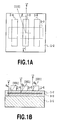
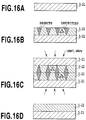
- Figs. 5A to 5C are diagrams illustrating conventional process-steps in producing a diamond semiconductor element. A description will be given below of the process-steps in producing a diamond semiconductor transistor by the use of a conventional technique disclosed in non-patent document 1 (see non-patent document 2 regarding surface orientation).
- a single-crystal diamond substrate 1-31 is prepared as shown in Fig. 5A .
- the surface orientation of the surface of the single-crystal diamond substrate 1-31, which is s ⁇ has its surface orientation preciously in the [001] direction.
- a two-dimensional-form hole channel 1-33 is formed in such a manner as to be parallel to the surface of the single-crystal diamond thin film 1-32.
- the surface orientation of the surface of the single-crystal diamond thin-film 1-32, which is d ⁇ , and, the surface orientation of the forming face of the hole channel 1-33, which is c ⁇ becomes equal to the surface orientation of the surface of the single-crystal diamond substrate 1-31, and thus has the surface orientation preciously in the [001] direction.
- a source electrode 1-34, a gate electrode 1-35, and a drain electrode 1-36 are all formed on the single-crystal diamond thin-film 1-32.
- the longitudinal direction of the gate electrode 1-35, which is g ⁇ , is the [100] direction.
- non-patent document 1 The characteristics of the transistor produced by the aforementioned conventional method are disclosed in detail in non-patent document 1.
- the transistor characteristics data on all items with reference to the characteristics of a transistor having a gate length of 0.2 ⁇ m (normalized by the gate width) is disclosed.
- the maximum transconductance gmmax of the transistor is 150mS/mm at the most.
- a diamond single-crystal has the problem of an extremely high density of a crystal defect as compared with that of another semiconductor, for example, silicone, gallium arsenide, indium phosphide, gallium nitride, and the like.
- another semiconductor for example, silicone, gallium arsenide, indium phosphide, gallium nitride, and the like.
- the natural physical properties of a diamond such as high thermal conductivity, a high breakdown electrical field, satisfactory high-frequency characteristics and the like, cannot be reflected in the transistor characteristics.
- a transistor using a diamond semiconductor is not yet in actual use. This problem is described in non-patent document 1. In consequence, for the achievement of the practically useful transistor using a diamond single-crystal, what is required is to produce an element by a method that minimizes the occurrence of the crystal defect peculiar to a diamond.
- a diamond has the highest thermal conductivity among materials and has the highest breakdown electric field strength among semiconductors, the diamond is the semiconductor material most suitable for a high-power semiconductor operable at high voltage and large current.
- the diamond is suitable for a high-frequency semiconductor element operable at high frequency.
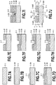
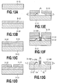
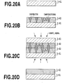
- Figs. 13A to 13G illustrate process-steps in producing a conventional diamond semiconductor element.
- Gold Au
- Fig. 13A diamond single-crystal thin-film 2-11
- Fig. 13B The Au thin-film 2-12 is coated with a resist 2-13 ( Fig. 13C ).
- photolithography or an electron beam is applied for exposure and development to remove part of the resist 2-13 to form an aperture in the resist 2-13 above the area in which a gate electrode will be formed ( Fig. 13D ).
- a sample is immersed in an Au etchant to etch a portion of the Au thin-film 2-12 close to the aperture in the resist 2-13 ( Fig. 13 E) .
- the etching is performed on the portion of the surface of the Au thin-film 2-12 exposed by the aperture of the resist 2-13, then proceeds from there in the depth direction (the direction at right angles to the diamond single-crystal thin-film 2-11) and simultaneously in the lateral direction (the direction horizontal to the diamond single-crystal thin-film 2-11). For this reason, an area of the Au thin-film 2-12 below the resist 2-13 is also cut away. The portion cut away or, as it were, hollowed out is called the "undercut" .
- Al aluminum
- Fig. 13F Al (aluminum) is evaporated.
- the Al which passes through the apertures of the resist 2-13 and the Au thin-film 2-12 to be evaporated directly onto the surface of the diamond single-crystal thin-film 2-11, and the Al, which is evaporated onto the resist 2-13, respectively form Al thin-films 2-15G, 2-15.
- a sample is immersed in a liftoff fluid for the liftoff of the resist 2-13 to remove the resist 2-13 and the Al thin-film 2-15 evaporated thereon ( Fig. 13G ).
- one of the Au thin-films 2-12 is defined as a source electrode 2-16S and the other thin-film 2-12 is defined as a drain electrode 2-16D, and also, the Al thin-film 2-15G remaining on the diamond single-crystal thin-film 2-11 is defined as a gate electrode 2-17G.
- the thickness t S , t D is 0. 6 ⁇ m
- the gate length d G corresponding to the length from the end of the gate electrode 2-17G close to the source to the end close to the drain is 0.2 ⁇ m.
- the diamond semiconductor has the physically derived limitation that the channels in which the electron and the hole of a transistor travel are required to be located within 0.1 ⁇ m from the surface unlike other semiconductors, for example, silicone, gallium arsenide, indium, gallium nitride, and the like (see non-patent document 3).
- a requirement for an increase in the transconductance g m , which is the degree of amplification of the diamond semiconductor element, to produce an enhancement up to a practical level in the maximum oscillation frequency f max , which is the upper limit to operation frequency in the high-frequency characteristics, is to reduce the source-gate electrode distance d SG between an end of the face of the source electrode 2-16S making contact with the diamond single-crystal thin-film 2-11 and the end of the gate electrode 2-17G close to the source, and the gate-drain electrode distance d GD between the end of the gate electrode 2-17G close to the drain and an end of the face of the drain electrode 2-16D making contact with the diamond single-crystal thin-film 2-11.
- Non-patent document 4 discloses that the source-gate electrode distance d SG and the gate-drain electrode distance d GD are respectively from 1.3 ⁇ m to 1.4 ⁇ m, because the distance between the source electrode 2-16S and the drain electrode 2-16D is 2.6 ⁇ m or 2.7 ⁇ m, and the gate length d G is 0.2 ⁇ m.
- the source electrode resistance and the drain electrode resistance are required to be reduced as much as possible.
- the thickness t S of the source electrode 2-16S and the thickness t D of the drain electrode 2-16D are required to be increased as much as possible.
- the inverted mesa structure having an angle ⁇ of about 45 degrees occurs at the end faces of the source electrode 2-16S and the drain electrode 2-16D close to the gate electrode 17G.
- the conventional art is incapable of simultaneously satisfying the two requirements, "a reduction in the source-gate electrode distance and the gate-drain electrode distance” and "an increase in the thickness of the source electrode and the thickness of the drain electrode”.
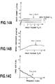
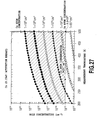
- Figs. 14A to 14C show the characteristics of a diamond transistor produced by a conventional process. They are the results disclosed in non-patent document 3, all of which are standardized with reference to the characteristics of a transistor having a gate length of 0.2 ⁇ m.
- the maximum drain current normalized by the gate length d G is 0.35A/mm at the most.
- the maximum transconductance g mmax normalized by the gage length d G is 150mS/mm at the most.
- the maximum oscillation frequency f max which is an upper limit to the operation frequency is 81GHz at the most.
- the drain breakdown voltage which is not shown in figures, is 45V at the most.
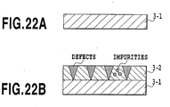
- a diamond single-crystal substrate 3-1 having surface orientation (100) is prepared ( Fig. 22A ).
- a microwave plasma CVD (chemical vapor deposition) apparatus is used to deposit a diamond single-crystal thin-film 3-2 of about 1 ⁇ m to 5 ⁇ m thickness onto the diamond single-crystal substrate 3-1 at a substrate temperature of 700°C using methane as a reaction gas ( Fig. 22B ).
- the surface of the diamond thin-film obtained by the CVD technique is hydrogen-terminated in an as-grown state and has surface conduction properties, and functions as a P-type semiconductor.
- Non-patent document 5 describes that, in order to improve the crystallinity of a diamond thin-film deposited on a silicone substrate, the above diamond thin-film is placed in a ceramic tube in which a vacuum of 1 ⁇ 10 -6 Torr is produced, and high-temperature annealing of 1000°C or more is performed in the vacuum.
- the diamond single-crystal thin-film produced by the process for producing the conventional diamond single-crystal thin-film described in Figs. 22A and 22B has an average mobility of about 800cm 2 /Vs at room temperature, and a high quality thin-film is obtained with satisfactory reproducibility.
- impurities and a large number of crystal defects such as a growth hillock, abnormal growth particles and the like exist in the above diamond single-crystal thin-film.
- the annealing is desirably performed at higher temperatures.
- the temperature is increased for an improvement in crystallinity, when the temperature reaches a certain degree (1200°C) or more, the conversion to graphite progresses in the diamond thin-film, resulting in an increase in deterioration in crystallinity.
- a diamond has physical characteristics as a semiconductor superior to those of silicon (Si). It is recognized in a theory that the diamond element has characteristics regarding high-temperature operation five times that of the Si element, high-voltage performance 30 times that of the Si element and an increase in speed three times that of the Si element. For this reason, it is expected that the diamond will realize a high-output device having a high thermal conductivity and a breakdown electric field strength, a high-frequency device having a high carrier mobility and a high saturated drift velocity, and the like. In other words, because a field-effect transistor (FET) or a bipolar transistor uses a diamond semiconductor, an electron element capable of driving at a high frequency for high-power operation, significantly exceeding the conventional semiconductors, is provide. In addition, it is clear in theory that the realization of a semiconductor laser and a light emitting diode using a diamond semiconductor realizes a high intensity light emitting element with a wavelength of 225nm in the ultraviolet region (see non-patent document 6).
- FET field-effect transistor
- a diamond has a band gap of 5. 5eV and is originally an insulator, but, as in the case of Si, if the diamond is doped with B which is a III group element, an acceptor level occurs, resulting logically in a p-type semiconductor.
- a p-type semiconductor layer in a transistor or optical device structure has a high resistance, as in the case of an insulator when the hole concentration is less than 1.0 ⁇ 10 15 cm -3 , the p-type semiconductor layer does not fully function as a p-type semiconductor, and is thus of no use. Also, since a p-type semiconductor layer in a transistor or optical device structure shows a metallic electrical conduction when the density of the dopant element exceeds 1.0 ⁇ 10 21 cm -3 , in this case, the p-type semiconductor layer also does not fully functions as a p-type semiconductor, and is thus of no use. Thus , in the p-type semiconductor layer the hole concentration is required to be 1.0 ⁇ 10 15 cm -3 or more and the dopant element concentration to be 1.0 ⁇ 10 21 cm -3 or less.
- the hole concentration and the dopant element concentration in a semiconductor depend on temperatures, it is important to satisfy the above requirements in operational temperatures around room temperature (300K) in order to ensure the practicality of the device.
- room temperature 300K
- operation in a high-temperature condition is particularly required. For this reason, there is a necessity to satisfy the above requirements in, for example, about 500K which is higher than room temperature.
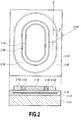
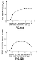
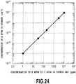
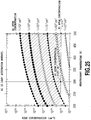
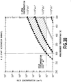
- the conventional technique of doping a diamond with boron (B) has the problem of only a hole concentration of 6 ⁇ 10 14 cm -3 being obtained at room temperature (300k) even when the B-atom concentration is 1.0 ⁇ 10 21 cm -3 .
- the horizontal axis represents the measurement temperature (K) and the vertical axis represents the hole concentration (cm -3 ) in a conventional p-type diamond semiconductor, in which the measured values at each B-atom concentration in the conventional p-type diamond semiconductor are plotted. These values do not satisfy the 1.0 ⁇ 10 15 cm -3 required for practical use at 300K. As a result, there arises the problem of the incapability of the practical use of a diamond semiconductor as a transistor or an optical device.
- a diamond is a semiconductor having both the highest thermal conductivity (22W/cmK) and the highest breakdown electric field (>10MV/cm) among substances as described above, and also a high carrier mobility (electron: 4500cm 2 /Vs, hole: 3800cm 2 /Vs), and if highly efficient doping is accomplished, a transistor operating at a high frequency and high output surpassing that of Si, GaAs, GaN is realized.
- the ion implantation technique is a method for accelerating impurities at high voltage so as to lend them energy of some kV to some MV for the introduction of impurity ions into the crystal, in which because a high energy process is involved, damage (crystal defects, amorphous layer and the like) occurs in the crystal in proportion to the acceleration voltage.
- the damage can be removed by performing appropriate high-temperature annealing treatment, with the result that the dopant is electrically activated and the semiconductor characteristics caused by the implanted impurities emerge.
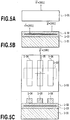
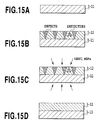
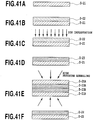
- Figs. 43A to 43E illustrate the process-steps in producing a diamond semiconductor using an ion implantation technique according to conventional art.
- An ion implantation apparatus is used to implant dopant (boron) into a diamond single-crystal ( Fig. 43A ) under the conditions of an acceleration voltage of 150kV and a dose of 1 ⁇ 10 16 cm -2 ( Figs. 43B to 43C ) and then firing (annealing) is performed for one hour at a pressure and a temperature of 5GPa and 1700K ( Fig. 43D ).
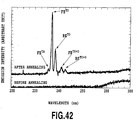
- the diamond thin-film subjected to the annealing treatment in this manner has a high resistance, thus giving rise to the problem of exhibiting no semiconductor characteristics. This is because etching occurs on the diamond surface during the process of the high-temperature and high-pressure annealing treatment so as to cut away the layer into which the ion is implanted ( Fig. 43D ). In this manner, the conventional technique has the problem of the impossibility of providing a diamond semiconductor because the diamond layer formed by ion implantation is etched during the high-temperature and high-pressure annealing.
- Patent document 1 Japanese Patent Publication No. 8-15162
- a [001] direction of the crystal axis of the single-crystal diamond thin-film is inclined with respect to surface orientation of a surface of the single-crystal diamond thin-film, or alternatively, a [001] direction of the crystal axis of the single-crystal diamond thin-film is inclined with respect to surface orientation of a forming face of the channel.
- the angle ad formed between the surface orientation of the surface of the single-crystal diamond thin-film and the [001] direction of the crystal axis of the single-crystal diamond thin-film, or the angle ac formed between the surface orientation of the forming face of the channel and the crystal axis [001] direction of the single-crystal diamond thin-film may be in the range of from 0.05 degrees to 1.1 degrees.
- a [001] direction of the crystal axis of the single-crystal diamond thin-film is inclined with respect to surface orientation of a surface of the single-crystal diamond thin-film, or alternatively, a [001] direction of the crystal axis of the single-crystal diamond thin-film is inclined with respect to surface orientation of a forming face of the channel.
- the angle ad formed between the surface orientation of the surface of the single-crystal diamond thin-film and the [001] direction of the crystal axis of the single-crystal diamond thin-film, or the angle ac formed between the surface orientation of the forming face of the channel and the [001] direction of the crystal axis of the single-crystal diamond thin-film may be in the range of from 0.05 degrees to 1.1 degrees.
- a field-effect transistor comprising a single-crystal diamond thin-film formed on a substrate, a hole or electron channel which is formed on the single-crystal diamond thin-film, and a drain electrode, a gate electrode and a source electrode which are formed on the channel, a [001] direction of the crystal axis of the single-crystal diamond thin-film is inclined with respect to surface orientation of a surface of the channel.
- the angle ⁇ c formed between the surface orientation of the surface of the channel and the [001] direction of the crystal axis of the single-crystal diamond thin-film may be in the range of from 0.05 degrees to 1.1 degrees.
- These substrates are a single-crystal diamond substrate, and the angle as formed between the surface orientation of an interface between the single-crystal diamond substrate and the single-crystal diamond thin-film and the [001] direction of the crystal axis of the single-crystal diamond thin-film may be in the range of from 0.05 degrees to 1.1 degrees.
- the angle ⁇ formed between the longitudinal direction of these gate electrodes and the [110] direction of the crystal axis of the single-crystal diamond thin-film may be in the range of from minus 30 degrees to plus 30 degrees.
- a process for producing a field-effect transistor comprising a single-crystal diamond thin-film formed on a substrate, a hole or electron channel which is formed inside the single-crystal diamond thin-film, and a drain electrode, a gate electrode and a source electrode which are formed on the single-crystal diamond thin-film, comprises the step of forming the single-crystal diamond thin-film on the substrate; the step of forming the channel on the single-crystal diamond thin-film; the step of further forming the single-crystal diamond thin-film on the channel thus formed; and the step of performing a grinding process on a surface of the single-crystal diamond thin-film in such a manner as to incline surface orientation of the surface of the single-crystal diamond thin-film with respect to the [001] direction of the crystal axis of the single-crystal diamond thin-film.
- a process for producing a field-effect transistor comprising a single-crystal diamond thin-film formed on a substrate, a hole or electron channel which is formed inside the single-crystal diamond thin-film, and a drain electrode, a gate electrode and a source electrode which are formed on the single-crystal diamond thin-film, comprises the step of forming the single-crystal diamond thin-film on the substrate; the step of performing a grinding process on a surface of the single-crystal diamond thin-film thus formed in such a manner as to incline the surface of the single-crystal diamond thin-film with respect to the [001] direction of a crystal axis of the single-crystal diamond thin-film; and the step of forming the channel on the single-crystal diamond thin-film after subjection to the grinding process.
- a process for producing a field-effect transistor comprising a single-crystal diamond thin-film formed on a single-crystal diamond substrate, a hole or electron channel which is formed inside the single-crystal diamond thin-film, and a drain electrode, a gate electrode and a source electrode which are formed on the single-crystal diamond thin-film, comprises the step of performing a grinding process on a surface of the single-crystal diamond substrate in such a manner as to incline surface orientation of the single-crystal diamond substrate with respect to the [001] direction of the crystal axis of the single-crystal diamond substrate; the step of forming the single-crystal diamond thin-film on the single-crystal diamond substrate after subjection to the grinding process; and the step of forming the channel on the single-crystal diamond thin-film.
- the surface orientation of conventional single-crystal diamond substrates points precisely in the [001] direction.
- the 001 surface orientation is a surface orientation in which defects occur extremely readily.
- the surface of the diamond substrate is shifted slightly from the [001] direction, thereby making it possible to significantly reduce the occurrence of crystal defects peculiar to a diamond.
- a high transconductance of the field-effect transistor is provided.
- a diamond semiconductor element which is characterized in that, in a diamond semiconductor element having a gate electrode, a source electrode and a drain electrode formed on a diamond single-crystal thin-film at a distance from each other, the source electrode includes a first area close to the diamond single-crystal thin-film and a second area except the first area, where a first distance between a first end face of the first area close to the gate electrode and the gate electrode is no more than a second distance between a second end face of the second area close to the gate electrode and the gate electrode, and the drain electrode includes a third area close to the diamond single-crystal thin-film and a fourth area except the third area, where a third distance between a third end face of the third area close to the gate electrode and the gate electrode is no more than a fourth distance between a fourth end face of the fourth area close to the gate electrode and the gate electrode.
- the first distance may be in the range of from 0.1 ⁇ m to 10 ⁇ m, and the second distance may be in the range of from the first distance to 30 ⁇ m.
- the third distance may be in the range of from 0.1 ⁇ m to 50 ⁇ m, and the fourth distance may be in the range of from the third distance to 50 ⁇ m.
- the thickness of the first area may be in the range of from 0.01 ⁇ m to 0.2 ⁇ m, and the thickness of the second area may be no less than 0.2 ⁇ m.
- the thickness of the third area may be in the range of from 0.01 ⁇ m to 0.2 ⁇ m, and the thickness of the fourth area may be no less than 0.2 ⁇ m.
- the source electrode includes, at least, a first lower metal film formed on the diamond single-crystal thin-film and a first upper metal film formed on the first lower metal film, where a first distance between a first end face of the first lower metal film close to the gate electrode and the gate electrode is no more than a second distance between a second end face of the first upper metal film close to the gate electrode and the gate electrode, and the drain electrode includes at least a second lower metal film formed on the diamond single-crystal thin-film and a second upper metal film formed on the second lower metal film, where a third distance between a third end face of the second lower metal film close to the gate electrode and the gate electrode is no more than a fourth distance between a fourth end face of the second upper metal film close to the gate electrode and the gate electrode.
- the first distance may be in the range of from 0.1 ⁇ m to 10 ⁇ m, and the second distance may be in the range of from the first distance to 30 ⁇ m.
- the third distance may be in the range of from 0.1 ⁇ m to 50 ⁇ m, and the fourth distance may be in the range of from the third distance to 50 ⁇ m.
- the thickness of the first lower metal film may be in the range of from 0.01 ⁇ m to 0.2 ⁇ m, and the thickness of the first upper metal film may be no less than 0.2 ⁇ m.
- the invention described in claim 10 is the diamond semiconductor element described in claims 6 to 9, which is characterized in that the thickness of the second lower metal film may be in the range of from 0.01 ⁇ m to 0.2 ⁇ m, and the thickness of the second upper metal film may be no less than 0.2 ⁇ m.
- the first lower metal film may be formed of either gold or an alloy including gold
- the first upper metal film may be formed either of any of the metals, gold, platinum, palladium, titanium, molybdenum and tungsten, or of an alloy including the metal.
- the second lower metal film may be formed of either gold or alloy including gold, and the second upper metal film may be formed either of any of the metals, gold, platinum, palladium, titanium, molybdenum and tungsten, or of an alloy including the metal.
- a process for producing a diamond semiconductor element comprising: the step of forming a first metal film on a diamond single-crystal thin-film; the step of forming a second metal film on the first metal film; the step of forming, in a first area of the second metal film, a first aperture reaching the surface of the first metal film; the step of etching away a part of the surface of the first metal film exposed by the aperture to form a second aperture reaching the surface of the diamond single-crystal thin-film; and the step of forming a third metal film on the diamond single-crystal thin-film exposed by the second aperture.
- the first aperture may be formed such that the width of the first aperture is larger than the thickness of the second metal film.
- the source electrode and the drain electrode are formed in such a manner as to divide each electrode into a layer for liftoff and a layer for etching, thereby making it possible to achieve the compatibility between "a reduction in the source-gate electrode distance and the gate-drain electrode distance” and “an increase in the thickness of the source electrode and the thickness of the drain electrode” to greatly improve the characteristics of a diamond field-effect transistor to reach a practical level.
- a process for producing a diamond thin-film which is characterized by comprising: a first process-step of forming a diamond crystal thin-film on a substrate; and a second process-step of firing the diamond crystal thin-film thus formed under a high pressure under which a diamond is stable.
- a process for producing a diamond thin-film which is characterized by comprising: a first process-step of forming a diamond crystal thin-film on a substrate; a second process-step of putting two of the diamond crystal thin-film thus formed in readiness; and a third process-step of firing the two diamond crystal thin-films, superimposed one on another such that surfaces of the two diamond crystal thin-films make at least partial contact with each other, under a high pressure under which a diamond is stable.
- a process for producing a diamond thin-film which is characterized by comprising: a first process-step of forming a diamond crystal thin-film on a substrate; a second process-step of either forming a protective member on at least a part of a surface of the diamond crystal thin-film thus formed, or overlaying the at-least part with a protective member, to use the protective member to protect the at-least part; and a third process-step of firing the diamond crystal thin-film thus protected by the protective member under a high pressure under which a diamond is stable.
- the protective member may be any one of the three, silicon oxide, silicon nitride or aluminum oxide.
- the protective member may be titanium, tungsten, platinum, palladium or molybdenum, or alternatively an alloy including at least one of them.
- the substrate may be a diamond single-crystal substrate.
- the diamond crystal thin-film may be a diamond single-crystal thin-film.
- Surface orientation of the diamond single-crystal substrate and the diamond single-crystal thin-film may be (111).
- the diamond crystal thin-film may be a diamond polycrystal thin-film.
- At least either control of temperature for heating the substrate when the diamond crystal thin-film is formed, or control of the ratio of the flow rate of methane to the flow rate of hydrogen in the methane and the hydrogen used when the diamond crystal thin-film is formed may be performed.
- the temperature may be controlled so as to be no less than growing temperatures when the diamond crystal thin-film is formed, and no more than 700°C.
- the ratio may be controlled so as to exceed 0% and to be no more than 0.5%.
- the smoothness of the surface of the diamond crystal thin-film may be no more than 30nm in a region of 1 ⁇ m 2 in terms of average square roughness.
- the relation between a pressure P(GPa) when the firing is carried out and a temperature T(K) when the firing is carried out may satisfy the relation of the expression P ⁇ 0.71+0.0027T, and also the firing may be carried out under a pressure of P ⁇ 1.5GPa.
- the diamond crystal thin-film may be formed by a microwave plasma CVD technique.
- the diamond crystal thin-film is subjected to high-pressure and high-temperature annealing treatment in such a manner as to make a diamond stable, thus making it possible to reduce the crystal defects and impurities in the diamond crystal thin-film, resulting in an increase in quality of the diamond crystal thin-film.
- a p-type diamond semiconductor which is characterized by comprising, as a dopant element, any of the elements, A1, Be, Ca, Cd, Ga, In, Li, Mg and Zn.
- the concentration of the dopant element may be a concentration enabling a hole concentration in the p-type diamond semiconductor to be no less than 1.0x10 15 cm -3 and also to be no more than 1.0x10 21 cm -3 at each temperature.
- A1 may be contained as the dopant element in a concentration of no less than 2.6 ⁇ 10 16 cm -3 and no more than 1.0 ⁇ 10 21 cm -3 .
- Be may be contained as the dopant element in a concentration of no less than 1.3 ⁇ 10 16 cm -3 and no more than 1.0 ⁇ 10 21 cm -3 .
- Ca may be contained as the dopant element in a concentration of no less than 3.2 ⁇ 10 16 cm -3 and no more than 1.0 ⁇ 10 21 cm -3 .
- Cd may be contained as the dopant element in a concentration of no less than 6.4 ⁇ 10 15 cm -3 and no more than 1.0 ⁇ 10 21 cm -3 .
- Ga may be contained as the dopant element in a concentration of no less than 8.1 ⁇ 10 15 cm -3 and no more than 1.0 ⁇ 10 21 cm -3 .
- In may be contained as the dopant element in a concentration of no less than 5.1 ⁇ 10 15 cm -3 and no more than 1.0 ⁇ 10 21 cm -3 .
- Li may be contained as the dopant element in a concentration of no less than 3.2 ⁇ 10 16 cm -3 and no more than 1.0 ⁇ 10 21 cm -3 .
- Mg may be contained as the dopant element in a concentration of no less than 1.0 ⁇ 10 17 cm -3 and no more than 1.0 ⁇ 10 21 cm -3 .
- Zn may be contained as the dopant element in a concentration of no less than 1.6 ⁇ 10 16 cm -3 and no more than 1.0 ⁇ 10 21 cm -3 .
- a process for producing a p-type diamond semiconductor which is characterized in that a diamond is doped with any of the elements Al, Be, Ca, Cd, Ga, In, Li, Mg and Zn by ultra-high-temperature and high-pressure synthesis.
- a process for producing a p-type diamond semiconductor which is characterized in that a diamond is doped with any of elements Al, Be, Ca, Cd, Ga, In, Li, Mg and Zn by ion implantation.
- a process for producing a p-type diamond semiconductor which is characterized in that a p-type diamond semiconductor film is grown, by a chemical vapor deposition (CVD) technique, on a diamond substrate from a source gas including, at least, a gas that includes carbon (C) and a dopant gas in which the ratio of the number of Al atoms to the number of C atoms (Al/C) is no less than 0.26ppm and no more than 10 4 ppm.
- CVD chemical vapor deposition
- the A1 dopant gas may include any of the following four: aluminum (Al) vaporized by introducing solid-state Al into plasma, trimethylaluminum ((CH 3 ) 3 Al: TMAI), triethylaluminum ((C 2 H 5 ) 3 Al: TEAI) and aluminium chloride (AlCl 3 ).
- a process of producing a p-type diamond semiconductor which is characterized in that, a p-type diamond semiconductor film is grown, by a chemical vapor deposition (CVD) technique, on a diamond substrate from a source gas including, at least, a gas that includes carbon (C) and a dopant gas in which the ratio of the number of Be atoms to the number of C atoms (Be/C) is no less than 0.13ppm and no more than 10 4 ppm.
- CVD chemical vapor deposition
- the Be dopant gas may include beryllium (Be) vaporized by introducing solid-state Be into plasma.
- Be beryllium
- a process of producing a p-type diamond semiconductor which is characterized in that, a p-type diamond semiconductor film is grown, by a chemical vapor deposition (CVD) technique, on a diamond substrate from a source gas including, at least, a gas that includes carbon (C) and a dopant gas in which the ratio of the number of Ca atoms to the number of C atoms (Ca/C) is no less than 0.32ppm and no more than 10 4 ppm.
- CVD chemical vapor deposition
- the Ca dopant gas may include either calcium (Ca) vaporized by introducing solid-state Ca into plasma, or calcium chloride (CaCl 2 ).
- a process for producing a p-type diamond semiconductor which is characterized in that a p-type diamond semiconductor film is grown, by a chemical vapor deposition (CVD) technique, on a diamond substrate from a source gas including, at least, a gas that includes carbon (C) and a dopant gas in which the ratio of the number of Cd atoms to the number of C atoms (Cd/C) is no less than 0.064ppm and no more than 10 4 ppm.
- CVD chemical vapor deposition
- the Cd dopant gas may include any of the following three: dimethylcadmium ((CH 3 ) 2 Cd: DMCd), diethylcadmium ((C 2 H 5 ) 2 Cd: DECd) and cadmium chloride (CdCl 2 ).
- a process for producing a p-type diamond semiconductor which is characterized in that a p-type diamond semiconductor film is grown, by a chemical vapor deposition (CVD) technique, on a diamond substrate from a source gas including, at least, a gas that includes carbon (C) and a dopant gas in which the ratio of the number of Ga atoms to the number of C atoms (Ga/C) is no less than 0.081ppm and no more than 10 4 ppm.
- CVD chemical vapor deposition
- the Ga dopant gas may include any of the following three: trimethylgallium ((CH 3 ) 3 Ga: TMGa), triethylgallium ((C 2 H 5 ) 3 Ga: TEGa) and gallium chloride (GaCl 3 ).
- a process for producing a p-type diamond semiconductor which is characterized in that a p-type diamond semiconductor film is grown, by a chemical vapor deposition (CVD) technique, on a diamond substrate from a source gas including, at least, a gas that includes carbon (C) and a dopant gas in which the ratio of the number of In atoms to the number of C atoms (In/C) is no less than 0.051ppm and no more than 10 4 ppm.
- CVD chemical vapor deposition
- the In dopant gas may include any of the following three: trimethylindium ((CH 3 ) 3 In: TMIn), triethylindium ((C 2 H 5 ) 3 In: TEIn) and indium chloride (InCl 3 ).
- a process for producing a p-type diamond semiconductor which is characterized in that a p-type diamond semiconductor film is grown, by a chemical vapor deposition (CVD) technique, on a diamond substrate from a source gas including, at least, a gas that includes carbon (C) and a dopant gas in which the ratio of the number of Li atoms to the number of C atoms (Li/C) is no less than 3.0ppm and no more than 10 4 ppm.
- CVD chemical vapor deposition
- the Li dopant gas may include any of the following three: methyllithium (CH 3 Li), ethyllithium (C 2 H 5 Li) and propyllithium (C 3 H 7 Li).
- a process for producing a p-type diamond semiconductor which is characterized in that a p-type diamond semiconductor film is grown, by a chemical vapor deposition (CVD) technique, on a diamond substrate from a source gas including, at least, a gas that includes carbon (C) and a dopant gas in which the ratio of the number of Mg atoms to the number of C atoms (Mg/C) is no less than 1.0ppm and no more than 10 4 ppm.
- CVD chemical vapor deposition
- the dopant gas including Mg may include any of the following three: bis-cyclopentadienyl magnesium ((C 5 H 5 ) 2 Mg: Cp 2 Mg), bis-methylcyclopentadienyl magnesium ((CH 3 C 5 H 4 ) 2 Mg: MCp 2 Mg) and magnesium chloride (MgCl 2 ).
- a process for producing a p-type diamond semiconductor which is characterized in that a p-type diamond semiconductor film is grown, by a chemical vapor deposition (CVD) technique, on a diamond substrate from a source gas including, at least, a gas that includes carbon (C) and a dopant gas in which the ratio of the number of Zn atoms to the number of C atoms (Zn/C) is no less than 0.16ppm and no more than 10 4 ppm.
- CVD chemical vapor deposition
- the dopant gas including Zn may include any of the following three: dimethylzinc ((CH 3 ) 2 Zn: DMZn), diethylzinc ((C 2 H 5 ) 2 Zn: DEZn) and zinc chloride (ZnCl 2 ).
- an MESFET which is characterized by comprising: a diamond substrate; the p-type diamond semiconductor layer, produced by any of the aforementioned processes, formed on the diamond substrate; a source electrode and a drain electrode formed on the p-type diamond semiconductor layer at a distance from each other; and a gate electrode formed between the source electrode and the drain electrode on the p-type diamond semiconductor layer.
- an MISFET which is characterized by comprising: a diamond substrate; the p-type diamond semiconductor layer, produced by any of the aforementioned processes, formed on the diamond substrate; a source electrode and a drain electrode formed on the p-type diamond semiconductor layer at a distance from each other; an insulating layer formed between the metal electrodes on the p-type diamond semiconductor layer: and a gate electrode formed on the insulating layer.
- an npn-type bipolar transistor which is characterized by comprising: a diamond substrate; a first n-type diamond semiconductor layer formed on the diamond substrate; the first p-type diamond semiconductor layer produced by any of the aforementioned processes, and a first metal electrode that are formed on the first n-type diamond semiconductor layer at a distance from each other; a second n-type diamond semiconductor layer and a second metal electrode that are formed on the p-type diamond semiconductor layer at a distance from each other; and a third metal electrode formed on the second n-type diamond semiconductor layer.
- a pnp-type bipolar transistor which is characterized by comprising: a diamond substrate; the first p-type diamond semiconductor layer, produced by any of the aforementioned processes, formed on the diamond substrate; an n-type diamond semiconductor layer and a first electrode that are formed on the first p-type diamond semiconductor layer at a distance from each other; the second p-type diamond semiconductor layer, produced by any of the aforementioned processes and formed on the diamond substrate, and a second electrode that are formed on the n-type diamond semiconductor layer at a distance from each other; and a third electrode formed on the second p-type diamond semiconductor layer.
- an LED which is characterized by comprising: a diamond substrate; the p-type diamond semiconductor layer, produced by any of the aforementioned processes, formed on the diamond substrate; an n-type diamond semiconductor layer and an anode electrode that are formed on the p-type diamond semiconductor layer at a distance from each other; and a cathode electrode formed on the n-type diamond semiconductor layer.
- a process for producing a diamond semiconductor comprises: a first process-step of implanting dopant into a diamond by an ion implantation technique; a second process-step of forming a protective layer on at least part of the surface of the ion-implanted diamond; and a third process-step of firing the ion-implanted diamond protected by the protective layer under a pressure of no less than 3.5GPa and at a temperature of no less than 600°C.
- a process for producing a diamond semiconductor by comprising: a first process-step of implanting dopant into a diamond by an ion implantation technique; and a second process-step of superimposing two of the ion-implanted diamond on one another such that at least part of the surfaces of the ion-implanted diamonds make contact with each other, and then of firing them under a pressure of no less than 3.5GPa and at a temperature of no less than 600°C.
- the dopant implanted by the ion implantation technique may include at least one of kinds, B, Al, Ga, In, Zn, Cd, Be, Mg, Ca, P, As, Sb, O, S, Se, Li, Na, and K.
- the pressure P (kbar) and the temperature T (K) when the ion-implanted diamond is fired may be a pressure of no less than 35kbar and a temperature of no less than 873K which satisfy the relation of the expression P>7.1+0.027T.
- the protective layer may be any of the following layers: a layer of a metal including at least one of the metals titanium, tungsten, platinum, palladium and molybdenum, a layer of Al 1-x Si x O 1-y N y (0 ⁇ x ⁇ 1, 0 ⁇ y ⁇ 1) and a layer comprising many layers of no less than two of them.
- the diamond used in the first process-step may be a diamond thin-film produced by a CVD technique.
- a diamond semiconductor element according to the present invention is characterized in that each surface orientation of a single-crystal diamond substrate, a single-crystal diamond thin-film, and a hole channel or electron channel, and the direction of forming a gate electrode are defined as directions peculiar to the present invention.
- the structure of a diamond semiconductor element according to the present invention in order to attain the first object and a process for producing the diamond semiconductor element will be described below in detail.
- Figs. 1A and 1B are schematic diagrams of a diamond semiconductor element according to embodiment 1 of the present invention. As illustrated in the sectional view in Fig. 1B , a single-crystal diamond thin-film 1-2 is formed on a single-crystal diamond substrate 1-1. A two-dimensional hole or electron channel 1-3 is formed in the single-crystal diamond thin-film 1-2.
- an angle formed by the surface orientation of the single-crystal diamond substrate 1-1 and the crystal axis [001] direction of the single-crystal diamond substrate 1-1 is defined as ⁇ s
- an angle formed by the surface orientation of the single-crystal diamond thin-film 1-2 and the crystal axis [001] direction of the single-crystal diamond thin-film 1-2 is defined as ⁇ d
- an angle formed by the surface orientation of the channel 1-3 and the crystal axis [001] direction of the single-crystal diamond thin-film 1-2 is defined as ⁇ c.
- a source electrode 1-4, a gate electrode 1-5 and a drain electrode 1-6 are formed on the surface of the single-crystal diamond thin-film 1-2.
- the channel 1-3 formed in the single-crystal diamond thin-film 1-2 is indicated with a dotted line.
- An angle formed by the longitudinal direction of the gate electrode 1-5, which is g ⁇ , and the crystal axis [110] of the single-crystal diamond thin-film is defined as ⁇ .
- ⁇ s, ⁇ d, ⁇ c and ⁇ will be given later.
- Figs. 3A to 3D are diagrams illustrating the process-steps in producing the diamond semiconductor element according to the present invention.
- a single-crystal diamond substrate 1-1 having surface orientation oriented mainly in the [001] direction of the crystal axis is prepared.
- surface grinding is performed such that the surface direction of the surface of the single-crystal diamond substrate 1-1, which is s ⁇ , is inclined ⁇ s (°) from the [001] direction of the crystal axis of the single-crystal diamond substrate 1-1.
- the surface grinding may be carried out by the following procedure, for example. First, the inclined angle from the [001] surface orientation of the substrate surface is measured in advance by X-ray diffraction measurement. Then, the single-crystal diamond substrate 1-1 is bonded to a sample tray with wax. Then, an iron flat plate is coated with diamond abrasive grain (particle diameter of from 0.3 ⁇ m to 1 ⁇ m) together with oil.
- the sample tray on which the single-crystal diamond substrate 1-1 is bonded is placed on the iron flat plate, and is then fixed, and then the iron flat plate is rotated for grinding. After grinding has been performed for a fixed time-period, the inclined angle is measured by X-ray diffraction measurement. The above-described grinding and the X-ray diffraction measurement are repeated until the desired angle ⁇ s is obtained. In other words, as shown in Fig. 3B , the substrate is cut away until the surface orientation of the single-crystal diamond substrate reaches a predetermined ⁇ s by grinding.
- the face inclined ⁇ s(°) may be only the face on which a single-crystal diamond thin-film will be grown in the next process-step described later.
- crystal growth is performed on the single-crystal diamond substrate 1-1 having the surface orientation angle ⁇ s to form a single-crystal diamond thin-film 1-2 thereon.
- This crystal growth of the thin-film may be carried out by, for example, a microwave plasma CVD technique. More specifically, a methane gas and a hydrogen gas (the flow ratio of methane gas is 1%) are fed as a source gas into a reaction tube in which the single-crystal diamond substrate 1-1 is placed. The degree of vacuum in the reaction tube is set at 50Torr, and a microwave is applied at 2.45GHz and 1.3kW to generate plasma in the reaction tube.
- the temperature of the single-crystal diamond substrate 1-1 is set at 700 degrees (all this is condition 1).
- the surface orientation of the surface of the single-crystal diamond thin-film 1-2, which is d ⁇ is able to be formed at an inclination of ⁇ d(°) from the [001] direction of the crystal axis of the single-crystal diamond thin-film 1-2, as in the case of the surface of the single-crystal diamond substrate 1-1.
- a two-dimensional hole or electron channel 1-3 is formed inside the single-crystal diamond thin-film 1-2 along the surface of the single-crystal diamond thin-film 1-2.
- the channel 1-3 is formed by, for example, a microwave plasma CVD technique as in the case of the aforementioned single-crystal diamond thin-film 1-2.
- the conditions of the temperature and the degree of vacuum in the reaction tube and the microwave are the same, but the condition of the source gas is changed so that only a hydrogen gas is used (condition 2). Under this condition 2, plasma is applied for 15 minutes to the surface of the single-crystal diamond thin-film 1-2 under the growing process, thereby forming the channel 1-3.
- the previous condition (condition 1) is restored, the single-crystal diamond thin-film 1-2 is formed again, thereby forming the channel 1-3 inside the single-crystal diamond thin-film 1-2.
- condition 1 and condition 2 apply to an example when a hole channel is used.
- an electron channel is used to constitute a diamond semiconductor element
- condition 3 the single-crystal diamond thin-film 1-2 is formed initially under condition 1, then the condition is changed to condition 3 to form an electron channel 1-3, and then the condition is changed back to condition 1 to form the single-crystal diamond thin-film 1-2 again.
- the surface orientation of the forming face of the two-dimensional channel 1-3 which is c ⁇ , is able to be formed at an inclination of ⁇ c(°) from the [001] direction of the crystal axis of the single-crystal diamond thin-film 1-2.
- a source electrode 1-4, a gate electrode 1-5 and a drain electrode 1-6 are formed on the surface of the single-crystal diamond thin-film 1-2.
- the channel 1-3 exists directly below the source electrode 1-4 and the drain electrode 1-6 (the channel 1-3 is indicated with the dotted line in the top view in Fig. 3D ).
- the gate electrode 1-5 is positioned midway between the source electrode 1-4 and the drain electrode 1-6.
- the gate electrode 1-5 is positioned so as to intersect with the channel 1-3.
- the gate electrode 1-5 is produced such that the longitudinal direction of the gate electrode 1-5 above the channel 1-3, which is g ⁇ , becomes the [001] direction of the crystal axis of the single-crystal diamond thin-film or a direction inclining ⁇ (degrees) from the [001] direction of the crystal axis, as shown in Fig. 3D .
- the field-effect transistor based on the diamond semiconductor element structure according to the present invention is completed.
- each of the angles can be independently controlled. For example, after the single-crystal diamond thin-film 1-2 is formed and before the electrodes are formed, the surface of the single-crystal diamond thin-film 1-2 is ground for inclination. Thereby, it is possible to make the angle ⁇ d and the angle ⁇ s different from each other.
- the substrate is temporarily removed from the reaction tube, and then the surface of the single-crystal diamond thin-film which has been formed up to that time is ground for inclination. Then, the channel 1-3 is formed. Thereby, it is possible to control ⁇ s and ⁇ c independently of each other.
- Figs. 4A and 4B are graphs showing the characteristics of the field-effect transistor produced by the above-described process-steps according to the present invention.
- Fig. 4A is a graph showing the relationship between the maximum transconductance gmmax and the angles ( ⁇ s, ⁇ d, ⁇ c) inclined from the [001] direction of orientation of each surface.
- the transconductance is a basic parameter representing the performance of the field-effect transistor. In general, the existence of crystal defects is able to be evaluated by the representative device performance gm. If the gm is high, fewer crystal defects can be evaluated. Note that the value of ⁇ in Fig. 4B , described later, is zero degrees.
- the surface orientation of the single-crystal diamond substrate or the like points precisely in the [001] direction.
- the gmmax is about 40mS/mm to about 80mS/mm.
- ⁇ s, ⁇ c and ⁇ d are within the range of 0.05° to 1.1°, the gmmax is 300mS/mm or more.
- ⁇ s, ⁇ c and ⁇ d exceed 1.1°, gmmax sharply decreases.
- the setting of ⁇ s, ⁇ c and ⁇ d within the range of 0.05° to 1.1° makes it possible to obtain a significantly higher gmmax than that in the case of conventional art.
- the shifting of the surface orientation of the single-crystal diamond substrate or the like slightly from the [001] direction makes it possible to remarkably suppress the occurrence of the crystal defects peculiar to a diamond, thus providing transconductance of a large field-effect transistor.
- the [100] direction is used for the longitudinal direction of the gate electrode.
- the gmmax is 25mS/mm at the most.
- the structure of the channel 1-3 is not limited to being placed exactly halfway in the thickness direction of the single-crystal diamond thin-film layer 1-2 as illustrated in Fig. 1B .
- the single-crystal diamond thin-film 1-2 has a relatively thicker film-thickness such that the film alone can structurally support itself alone.
- the removal of the single-crystal diamond substrate 1-1 may be performed by, for example, grinding.
- the [110] direction and the [100] direction are the definition of the direction when a principal direction of the plane of the single-crystal diamond substrate 1-1 or the principal direction of the surface of the single-crystal diamond thin-film 1-2 is designated as the [001] direction.
- a diamond crystallographically has the lattice system, which is a cubic lattice (cubic crystal).
- the crystal plane has the property of being apt to appear as the number of atom bonds necessary to be broken when the plane is formed becomes fewer. For this reason, in the case of a diamond, the surface orientations apt to appear are [001], [111] and [011].
- the [100] direction which is a preferable direction of the longitudinal direction of the gate electrode 1-5
- the description of the [100] direction in this specification includes the [010] direction.
- [100], [-100], [010], [0-10], [00-1] are equivalent as described earlier, and they are generically referred to as the [100] direction which is a preferable direction of the longitudinal direction of the gate electrode 1-5.
- the [110] direction also is a generic name.
- the single-crystal diamond substrate 1-1 is used.
- the single-crystal diamond substrate 1-1 is not used, as long as the surface orientation of the single-crystal diamond thin-film 1-2 or the surface orientation of the channel 1-3 plane falls within each of the ⁇ d, ⁇ c angle ranges described in Fig. 4 , it is needless to say that the effect of increasing the transconductance is produced by the same token.
- Ir iridium metal
- MgO, Si for example, may be used as a substrate. What is required is for the substrate to allow the single-crystal diamond thin-film to be formed thereon.
- Fig. 2 is a diagram illustrating the structure of a diamond semiconductor element according to embodiment 2 of the present invention.
- the structure of embodiment 2 is suitable for high power operation.
- a gate electrode is arranged in the form of a sport ground track.
- a single-crystal diamond thin-film 1-12 is formed on a single-crystal diamond substrate 1-11 and a two-dimensional hole or electron channel 1-13 is formed inside the single-crystal diamond thin-film.
- the channel has an oval shape.
- a source electrode 1-14, a gate electrode 1-15 and a drain electrode 1-16 are formed on the surface of the single-crystal diamond thin-film 1-12 above the channel 1-13.
- the gate electrode 1-15 and the source electrode 1-14 are arranged outward in order so as to encircle the periphery of the oval-shaped drain electrode 1-16 placed innermost.
- Fig. 2 does not clearly show, but in embodiment 2, the surface orientations of the single-crystal diamond substrate 1-11, the single-crystal diamond thin-film 1-12 and the channel 1-13 are also set respectively at ⁇ s, ⁇ d, ⁇ c falling within the same range as in the case of embodiment 1.
- Each of the electrodes is placed such that in the linear area, except for the two arc portions corresponding to the two ends of the oval shape, the longitudinal direction of the gate electrode 1-15 is inclined ⁇ degrees from the crystal axis [110] direction. It is needless to say that the effect of increasing the transconductance is produced as in the case shown in Fig. 4 .
- Figs. 7A to 7J illustrate process-steps in producing a diamond semiconductor element according to an embodiment of the present invention.
- a thin-film 2-1 which is a diamond single-crystal and has a two-dimensional hole channel extending parallel to the surface, (hereinafter referred to as "diamond single-crystal thin-film 2-1") is prepared ( Fig. 7A ).
- Au is evaporated to a thickness of 0.1 ⁇ m onto the entire surface of the diamond single-crystal thin-film 2-1 to form an Au thin-film 2-2B ( Fig. 7B ).
- the Au thin-film 2-2B is coated with a resist 2-3 with a width of 20 ⁇ m in the area in which a gate electrode will be provided ( Fig. 7C ), and from the above, an Au thin-film 2-2T is evaporated onto the entire surface of the sample ( Fig. 7D ).
- the thickness of the Au thin-film 2-2T is 0.4 ⁇ m.
- Exposure and development are performed on an area having a width of 0.05 ⁇ m, in which a gate electrode will be formed, within the area of the resist 2-4 in contact with the Au thin-film 2-2B, to remove part of the resist 2-4 and to form an aperture 2-8 in the Au thin-film 2-2B ( Fig. 7G ).
- an etching solution is used to etch the part of the Au thin-film 2-2B exposed by the aperture 2-8 ( Fig. 7H ). Because etching takes place in an isotropic manner, the area of the Au thin-film 2-2B under the resist 2-4 is also etched to produce an undercut. The etching is terminated before reaching the Au thin-film 2-2T.
- Al is evaporated onto the full surface of the sample ( Fig. 7I ).
- Part of the Al is evaporated onto the diamond single-crystal thin-film 2-1 from the aperture 2-8 in the Au thin-film 2-2B so as to form an Al thin-film 2-5G.
- the remaining major portion of the Al is evaporated onto the resist 2-4 so as to form an Al thin-film 2-5.
- liftoff is performed on the resist 2-4 to remove the resist 2-4 and the Al thin-film 2-5 placed on the resist 2-4 ( Fig. 7J ).
- one of the Au thin-films 2-2B is defined as a lower source electrode 2-6SB, and the other is defined as a lower drain electrode 2-6DB.
- the Au thin-film 2-2T on the lower source electrode 2-6SB is defined as an upper source electrode 2-6ST
- the Au thin-film 2-2T on the lower drain electrode 2-6DB is defined as an upper drain electrode 2-6DT.
- this specification describes the lower source electrode and the upper source electrode as two separate ones, but the lower source electrode 2-6SB and the upper source electrode 2-6ST together function as a single source electrode in upper and lower combination.
- the lower source electrode 2-6SB and the upper source electrode 2-6ST may be considered to constitute a single source electrode.
- the lower drain electrode and the upper drain electrode may be considered to constitute a single drain electrode.
- the Al thin-film 2-5G is defined as a gate electrode 2-7G.
- the diamond single-crystal thin-film 2-1 may be of either single-crystal or polycrystal, and the channel formed in the diamond single-crystal thin-film 2-1 may be for either an electron or a hole.
- the gate length is defined as d G .
- the lower source to gate distance between the end of the lower source electrode 2-6SB in contact with the surface of the diamond single-crystal thin-film 2-1 and the end of the gate electrode 2-7G close to the source is defined as d SGB .
- the gate to lower drain distance between the end of the lower drain electrode 2-6DB in contact with the surface of the diamond single-crystal thin-film 2-1 and the end of the gate electrode 2-7G close to the drain is defined as d GDB .
- the upper source to gate distance between the end of the upper source electrode 2-6ST and the end of the gate electrode 2-7G close to the source is defined as d SGT .
- the gate to upper drain distance between the end of the upper drain electrode 2-6DT and the end of the gate electrode 2-7G close to the drain is defined as d GDT .
- the thickness of the entire source electrode is defined as t S , in which the thickness of the lower source electrode 2-6SB is defined as t SB , and the thickness of the upper source electrode 2-6ST is defined as t ST .
- the thickness of the entire drain electrode is defined as t D , in which the thickness of the lower drain electrode 2-6DB is defined as t DB , and the thickness of the upper drain electrode 2-6DB is defined as t DT .
- the source electrode and the drain electrode are divided into a layer to be etched using an etching solution and a layer subject to liftoff using resist.
- the inverted mesa portion of the electrode is reduced in size. This makes it possible to shorten the distance between the source electrode and the gate electrode to increase the maximum oscillation frequency f max , and also to increase the thickness of the source electrode and the drain electrode to bring the drop in voltage down to a small value.
- the source electrode and the drain electrode are each constituted of a metal film made up of two layers, the Au thin-film 2-2T which is an upper metal film and the Au thin-film 2-2B which is a lower metal film, but the source electrode and the drain electrode may be made up of a number of layers as long as a reduction in the thickness of the metal film in contact with the diamond single-crystal thin-film 2-1 is possible.
- the lower source electrode 2-6SB and the lower drain electrode 2-6DB have the ends close to the gate electrode 2-7G formed in an inverted mesa shape.
- a matter of importance for the present invention is to independently form the layer for "reducing the source-gate electrode distance and the gate-drain electrode distance" , and the layer for "increasing the thickness of the source electrode and the thickness of the drain electrode".
- the structure of the ends of the lower source electrode 2-6SB and the lower drain electrode 2-6DB closer to the gate electrode 2-7G is not limited to the inverted mesa structure.
- Figs. 8A to 8C show the characteristics of a diamond field-effect transistor using the diamond semiconductor element according to an embodiment of the present invention.
- Fig. 8A shows the drain current-voltage characteristics of the diamond field-effect transistor according to the embodiment.
- the maximum drain current I Dmax is 0.35A/mm in a conventional type, but reaches 1A/mm in the embodiment.
- Fig. 8B shows the dependence of the transconductance g m on the gate voltage V G (transfer characteristics) in the diamond field-effect transistor according to the embodiment.
- the maximum transconductance g mmax is 150mS/mm in a conventional type, but reaches 520mS/mm in the embodiment.
- Fig. 8C shows the dependence of the power gain U on the frequency f in the diamond field-effect transistor according to the embodiment. As shown in Fig. 8C , the maximum oscillation frequency f max is 81GHz in a conventional type, but reaches 310GHz in the embodiment.
- the diamond semiconductor element according to an embodiment of the present invention is greatly improved in the field-effect transistor characteristics as compared with that in a conventional diamond semiconductor element, and makes possible a diamond transistor with a practical level.
- the distance of the portion of the gate electrode 2-7G making contact with the surface of the diamond single-crystal thin-film is defined as gate length d G .
- the lower source-gate distance d SGB and the upper source-gate distance d SGT are respectively defined as the distance from the end of the gate electrode 2-7G which is closer to the source and makes contact with the surface of the diamond single-crystal thin-film 2-1, to the lower source electrode 2-6SB and the upper source electrode 2-6ST.
- the gate-lower drain distance d GDB and the gate-upper drain distance d GDT are respectively defined as the distance from the end of the gate electrode 2-7G which is closer to the drain and makes in contact with the surface of the diamond single-crystal thin-film 2-1, to the lower drain electrode 2-6DB and the upper drain electrode 2-6DT.
- Fig. 9A shows the relationship between the lower source-gate distance d SGB and the maximum oscillation frequency f max .
- Fig. 9B shows the relationship between the upper source-gate distance d SGT and the maximum oscillation frequency f max .
- Fig. 10A shows the relationship between the gate-lower drain distance d GDB and the drain breakdown voltage V BR .
- the V BR With an increase in the d GDB , the V BR increases, but the V BR sharply increases when the d GDB is in about from 0.05 ⁇ m to about 0.1 ⁇ m, and then the V BR becomes 100V or more when the d GDB is in a region of 0.1 ⁇ m or more, thus making it possible to provide satisfactory characteristics as compared with the case in the conventional structure where the V BR is 45V.
- the d GDB exceeds 50 ⁇ m, the f max decreases.
- Fig. 10B shows the relationship between the gate-upper drain distance d GDT and the maximum oscillation frequency f max .
- the f max increases until the d GDT becomes 3 ⁇ m, but after the d GDT exceeds 3 ⁇ m, the f max decreases.
- the f max shows 140GHz, thus making it possible to provide satisfactory characteristics as compared with the case in the conventional structure where the f max is 81GHz.
- Fig. 11A shows the relationship between the thickness t SB of the lower source electrode 2-6SB and the maximum oscillation frequency f max .
- the f max decreases, but when the t SB increases from 0.01 ⁇ m to 0.2 ⁇ m, the decrease in the f max is confined to from 260GHz to 130GHz, thus making it possible to provide satisfactory characteristics as compared with the case in the conventional structure where the f max is 81GHz.
- Fig. 11B shows the relationship between the thickness t ST of the upper source electrode 2-6ST and the maximum oscillation frequency f max .
- the f max With an increase in the t ST , the f max also increases, but when the t ST is 0.2 ⁇ m, the f max is 100GHz. When the t ST is 100 ⁇ m, the f max reaches 270GHz. Thereby, it is possible to provide satisfactory characteristics as compared with the case in the conventional structure where the f max is 81GHz.
- Fig. 12A shows the relationship between the thickness t DB of the lower drain electrode 2-6DB and the maximum oscillation frequency f max .
- the f max decreases, but when the t DB increases from 0.01 ⁇ m to 0.2 ⁇ m, the decrease in the f max is confined to from 300GHz to 100GHz, thus making it possible to provide satisfactory characteristics as compared with the case in the conventional structure where the f max is 81GHz.
- Fig. 12B shows the relationship between the thickness t DT of the upper drain electrode 2-6DB and the maximum oscillation frequency f max .
- the f max increases, but when the t DT is 0.2 ⁇ m, the f max is 100GHz, and when the t DT is 100 ⁇ m, the f max reaches 280GHz. Thereby, it is possible to provide satisfactory characteristics as compared with the case in the conventional structure where the f max is 81GHz.
- Table 1 shows the maximum oscillation frequencies f max of a conventional diamond semiconductor element using Au as a material for a source electrode and a drain electrode, and of a diamond semiconductor element according to an embodiment of the present invention using an AuPt alloy as a material for the lower source electrode 2-6SB and the lower drain electrode 2-6DB.
- the material for the upper source electrode 2-6ST and the upper drain electrode 2-6DT is Au.
- Electrode Material and Transistor Characteristics Electrode material Maximum oscillation frequency (GHz) Au (gold) conventional art 81 Au (gold) Pt (platinum) alloy 220
- the material for the lower source electrode 2-6SB and the lower drain electrode 2-6DB is Au.
- the above diamond semiconductor element uses Au for the electrode material, but the electrode materials shown in Table 2 are used for the electrode material of the diamond semiconductor element according to an embodiment of the present invention, resulting in a dramatic increase in f max .
- Electrode Material and Transistor Characteristics Electrode material Maximum oscillation frequency (GHz) Au (gold) conventional art 81 Au (gold) Pt (platinum) alloy 112 Pt (platinum) 141 Pd (palladium) 185 Ti (titanium) 153 Mo (molybdenum) 159 W (tungsten) 143
- the lower source electrode 2-6SB and the lower drain electrode 2-6DB may be formed of a material different from that of the upper source electrode 2-6ST and the upper drain electrode 2-6DT.
- An embodiment of the present invention has the key feature in that a diamond crystal thin-film is fired (annealed) at a sufficient temperature under high pressure under which a diamond is stable.
- a trial attempt for improving the crystallinity of a diamond crystal thin-film has been made using high-temperature annealing in a vacuum at 1000°C or more (see non-patent document 5), but deterioration occurs in high-temperature vacuum annealing because a diamond is basically stable under an extremely high pressure of 1.5Gpa or more.
- annealing is performed under high pressures under which a diamond is stable. Thereby, lattice defects included in a crystal, and the like are recovered or removed, thus enabling an enhancement in quality of the diamond crystal thin-film.
- (a diamond is) stable or stably means the condition in which the diamond maintains its diamond state without conversion to graphite.
- a diamond is stable means a condition in which the diamond maintains its diamond state without conversion to graphite even when being subjected to annealing at high temperatures and high pressures. This is, for example, in the case of diamond of a single crystal, a condition in which a diamond single-crystal maintains its single-crystal state without conversion to graphite. Therefore, the diamond crystal thin-film is annealed under high pressures in such a manner as to allow the diamond to be in its stable state, thereby preventing or reducing the conversion of the diamond crystal thin-film to graphite.
- a temperature (also called annealing temperature) T for performing annealing and a pressure (also called annealing pressure) P for performing annealing are determined within a region in which a diamond can be stably annealed.
- the relational expression P ⁇ 0.71+0.0027T is well known to persons skilled in the art.
- a more preferable temperature T is 550°C.
- the symbol O and the symbol x indicate the conditions under which high-pressure and high-temperature annealing is performed on the diamond crystal thin-film.
- the symbol O represents the condition under which the diamond structure is still stable after the annealing
- the symbol x represents the condition under which the diamond substrate is converted to graphite after the annealing.
- the annealing temperature and the annealing pressure are set within the foregoing region, in other words, if the annealing temperature and the annealing pressure, under which a diamond is stable, are set, it is possible to reduce the deterioration of the diamond crystal thin-film. Even when a higher annealing temperature is set, by increasing the annealing pressure, the condition will fall within the foregoing region, thus making it possible to set a higher annealing temperature. Thus, a decrease in crystal defects becomes possible. In consequence, according to the embodiment of the present invention, it is possible to achieve an improvement in quality of the diamond crystal thin-film.
- a diamond crystal thin-film is formed on a diamond single-crystal substrate by use of a microwave plasma CVD apparatus or the like, and then the diamond single-crystal substrate with the diamond crystal thin-film formed thereon is placed in an ultra-high-pressure and high-temperature firing furnace for performing the above-described annealing.
- Two diamond single-crystal substrates with the above-described diamond crystal thin-films formed thereon are prepared, then the two substrates are superimposed each other such that the surfaces of the respective diamond crystal thin-films (the face of each diamond crystal thin-film opposite to the interface between the diamond single-crystal substrate and the diamond crystal thin-film formed thereon) are in contact with each other, and then annealing may be performed.
- the two substrates may be superimposed such that at least parts of the surfaces of the two diamond crystal thin-films are in contact with each other. By such superimposition, the area of the surface of the diamond crystal thin-film exposed to air during the annealing disappears or is reduced, thus making it possible to lessen the effects of oxygen, nitrogen and moisture vapor in the air.
- the periphery of the sample is surrounded by NaCl and the like during the annealing because pressure is applied thereto, but the above superimposition makes it possible to lessen the adhesion of NaCl and the like to the surface of the diamond crystal thin-film during the annealing.
- each of the two diamond crystal thin-films can function as a protective member for the other diamond crystal thin-film.
- at least a part of the surface of one of the diamond crystal thin-films is in contact with at least a part of the surface of the other diamond crystal thin-film, whereby one diamond crystal thin-film overlies the contact area of the other.
- a protective member such as an insulating thin-film, a metal thin-film or an alloy, may be formed on at least a part of the surface of the diamond crystal thin-film and then the annealing may be performed. Because at least a part of the surface of the diamond crystal thin-film is overlaid with the protective member in this manner and then the annealing is performed, it is possible to lessen the effects of oxygen, nitrogen and moisture vapor in the air during the annealing, as in the above-described case of superimposing the substrates each other. Also, it is possible to lessen the adhesion of NaCl and the like to the surface of the diamond crystal thin-film during the annealing.
- the "protective member” is a member for lessening the effects of each component in the air, and of the materials such as NaCl and the like used for the application of pressure, on the surface of the diamond crystal thin-film.
- the protective member exerts its function by overlying or by being formed on at least a part of the surface of the diamond crystal thin-film.
- the existence of the protective member on the diamond crystal thin-film makes it possible to prevent or lessen the contact and adhesion of the components of the air, such as oxygen, nitrogen and moisture vapor, and of materials such as NaCl used for the application of pressure, to the surface of the diamond crystal thin-film.
- the substrate on which the diamond crystal thin-film is formed is not limited to the diamond single-crystal substrate.
- another substrate such as a diamond polycrystal substrate or a silicone substrate may be used.
- the diamond crystal thin-film formed on the substrate may be a diamond single-crystal thin-film or a diamond polycrystal thin-film.
- a process for producing a diamond thin-film according to an embodiment of the present invention will be described below in detail on the basis of embodiment examples, but it goes without saying that the present invention is not limited to the embodiment examples, and many changes and variations can be made without departing from the scope of the present invention.
- the diamond single-crystal thin-film may have any thickness, and is not limited to the values described in the following embodiment examples.
- a process for producing a diamond thin-film according to embodiment example 1 of the present invention will be described using Figs. 15A to 15D .
- a diamond single-crystal substrate 3-11 having surface orientation (100) is prepared ( Fig. 15A ).
- a microwave plasma CVD apparatus is used to deposit a diamond single-crystal thin-film 3-12 of about 1 - 5 ⁇ m thickness onto the diamond single-crystal substrate 3-11 at a substrate temperature of 700°C by use of methane as a reaction gas ( Fig. 15B ).
- the diamond single-crystal thin-film formed in such a manner may possibly include defects and/or impurities.
- the microwave plasma CVD apparatus is used, but any growing technique may be used as long as it can form a diamond thin-film.
- the diamond single-crystal substrate 3-11 having the diamond single-crystal thin-film 3-12 formed thereon is placed in an ultra-high-pressure and high-temperature firing furnace to anneal the diamond single-crystal thin-film 3-12 under the conditions of 1200°C and 6GPa ( Fig. 15C ).
- a high-quality diamond crystal thin-film with decreased defects and impurities can be obtained by the annealing ( Fig. 15D ).
- a diamond single-crystal substrate having a diamond crystal thin-film formed thereon is annealed under conditions of various temperatures and pressures as shown in Fig. 21 , in which the conditions of 1200°C and 6GPa is positioned in the region where a diamond can be stably annealed.
- the holes in the diamond crystal thin-film are measured before and after the high-pressure and high-temperature annealing for a comparison of characteristics.
- the mobility of the semiconductor which is obtained by the hole measurement is closely associated with the crystallinity, and the better the crystallinity, the more the mobility increases.
- some samples are produced under the same condition in order to reduce the variation between the samples, and the hole measurement is carried out to obtain an average value of the mobility (the average mobility).
- the average mobility of the yet-to-be-annealed sample ( Fig. 15B ), or the sample produced by a conventional process, at room temperature is about 800cm 2 /Vs.
- the average mobility of the sample subjected to the high-pressure and high-temperature annealing ( Fig. 15D ) is 1000cm 2 /Vs, resulting in an increase in the average mobility.
- the diamond crystal thin-films before and after the high-temperature and high-pressure annealing process are used to produce a field-effect transistor (FET), and current-voltage (Ids-Vds) measurement is conducted for a comparison of characteristics ( Figs. 23 ).
- FET field-effect transistor
- Ids-Vds current-voltage measurement
- Figs. 23 current-voltage measurement is conducted for a comparison of characteristics.
- gold is used as source and drain electrodes and aluminum is used as a gate electrode.
- the gate length is 5 ⁇ m and the gate width is 100 ⁇ m.
- the gate voltage is 0 - 3.5V and is measured in 0.5V steps.
- a process for producing a diamond thin-film according to embodiment example 2 of the present invention will be described using Figs. 16A to 16D .
- a diamond single-crystal substrate 3-21 having surface orientation (100) is prepared ( Fig. 16A ).
- a microwave plasma CVD apparatus is used to deposit a diamond single-crystal thin-film 3-22 of about 1 ⁇ m to about 5 ⁇ m thickness onto the diamond single-crystal substrate 3-21 at a substrate temperature of 700°C by use of methane as a reaction gas ( Fig. 16B ).
- the diamond single-crystal thin-film thus formed may possibly include defects and/or impurities.
- two diamond single-crystal substrates 3-21 having the diamond single-crystal thin-films 3-22 formed as described above are prepared.
- the two substrates are superimposed each other such that, as illustrated in Fig. 16C , the surfaces of the respective diamond single-crystal thin-films 3-22 face inwardly, that is, such that the surfaces of the two diamond single-crystal thin-films 3-22 make contact with each other, and then the superimposed substrates are placed in an ultra-high-pressure and high-temperature firing furnace and then annealed under the conditions of 1200°C and 6GPa.
- the above-described superimposition may be carried out by hand or alternatively by use of positioning means having means for picking up the substrate and putting it in position, and driving means for driving the means.
- the driving means such as a motor is operated to pick up one of the diamond single-crystal substrate 3-21 and place it onto the other diamond single-crystal substrate 3-21 such that the surfaces of the two diamond single-crystal thin-films 3-22 are aligned in contact with each other.
- any means may be used as long as the substrates can be superimposed in such a manner as to make contact between the surfaces of the two diamond single-crystal thin-films 3-22.
- the two superimposed substrates are separated from each other, and high-quality diamond crystal thin-films reduced in defects and impurities through the above-described annealing are obtained ( Fig. 16D ).
- the surfaces of the diamond crystal thin-film are in contact with each other during the annealing process, which makes it possible to lessen the effects of oxygen, nitrogen, moisture vapor and the like in the air on the diamond crystal thin-film.
- the above superimposition makes it possible to lessen the adhesion of NaCl, which is disposed around the substrate for the application of pressure, to the surface of the diamond crystal thin-film during the annealing.
- the embodiment example has described the superimposition of the surfaces of the two diamond single-crystal thin-films 3-22 each other with their whole surfaces making contact with each other, but is not limited to this. What is important in the embodiment example is to lessen the effects of each component of the air, NaCl used for the application of pressure, and the like on the surface of the diamond single-crystal thin-film 3-22 during the annealing, and for this end, a matter of importance is that no part of the surface is exposed during the annealing. Thus, in an embodiment example of the invention, if the two substrates are superimposed such that at least parts of the surfaces of the two diamond crystal thin-films make at least partial contact with each other, the foregoing effects are lessened.
- annealing may be performed by placing a diamond crystal substrate or oxides, nitrides, metal, alloy or the like, described in embodiment examples 3 and 4, as a protective member on at least a part of the diamond crystal thin-film, so as to overlie at least the part with the protective member.
- a process for producing a diamond thin-film according to embodiment example 3 of the present invention will be described using Figs. 17A to 17F .
- a diamond single-crystal substrate 3-31 having surface orientation (100) is prepared ( Fig. 17A ).
- a microwave plasma CVD apparatus is used to deposit a diamond single-crystal thin-film 3-32 of about 1 ⁇ m to about 5 ⁇ m thickness onto the diamond single-crystal substrate 3-31 at a substrate temperature 700°C by use of methane as a reaction gas ( Fig. 17B ).
- the diamond single-crystal thin-film thus formed may possibly include defects and/or impurities.
- a protective film 3-33 as the protective member is formed on the diamond single-crystal thin-film 3-32 as illustrated in Fig. 17C .
- the protective film 3-33 may be formed of various metallic compounds having a film-thickness of about 0.5 ⁇ m.
- Examples of the material for the protective film 3-33 include, but are not limited to, silicon monoxide (SiO x ), silicon nitride (SiN x ), aluminum oxide (AlO x ) and the like. These silicon monoxide, silicon nitride, aluminum oxide may be formed by an ECR spattering technique.
- the diamond single-crystal substrate 3-31 with the protective film 3-33 and the diamond single-crystal thin-film 3-32 formed thereon is placed in an ultra-high-pressure and high-temperature firing furnace, to anneal the diamond single-crystal thin-film 3-32 under the conditions of 1200°C and 6GPa ( Fig. 17D ).
- a high-quality diamond crystal thin-film with reduced defects and impurities is obtained ( Fig. 17E ).
- etching is performed for removing the protective film 3-33 ( Fig. 17F ).
- the defects in the diamond crystal thin-film are reduced by the high-pressure and high-temperature annealing, thus increasing the quality of the diamond crystal thin-film.
- the protective film is formed on the diamond crystal thin-film, it is possible during the annealing to lessen the effects of nitrogen, oxygen, moisture vapor and the like in the air on the surface of the diamond crystal thin-film.
- the aforementioned protective film makes it possible to lessen the adhesion of NaCl, which is disposed around the substrate for the application of pressure, to the surface of the diamond crystal thin-film during the annealing.
- the embodiment example has described the formation of the protective film 3-33 on the full surface of the diamond single-crystal thin-film 3-32, but is not limited to this. What is important in the embodiment example is to lessen the effects of each component of the air, NaCl used for the application of pressure, and the like on the surface of the diamond single-crystal thin-film 3-32 during the annealing, and for this end, a matter of importance is that no part of the surface is exposed during the annealing. Thus, in an embodiment example of the invention, if a protective film is formed on at least a part of the diamond single-crystal thin-film, the foregoing effects can be lessened.
- a process for producing a diamond thin-film according to embodiment example 4 of the present invention will be described using Figs. 18A to 18F .
- a diamond single-crystal substrate 3-41 having surface orientation (100) is prepared ( Fig. 18A ).
- a microwave plasma CVD apparatus is used to deposit a diamond single-crystal thin-film 3-42 of about 1 ⁇ m to about 5 ⁇ m thickness onto the diamond single-crystal substrate 3-41 at a substrate temperature 700°C by use of methane as a reaction gas ( Fig. 18B ).
- the diamond single-crystal thin-film thus formed may possibly include defects and/or impurities.
- a protective film 3-43 as a protective member is formed on the diamond single-crystal thin-film 3-42 as illustrated in Fig. 18C .
- various metallic films or alloy films having a film-thickness of about 0.5 ⁇ m may be used.
- the material for the protective film 3-43 include, but are not limited to, platinum (Pt), titanium (Ti), tungsten (W), palladium (Pd), molybdenum (Mo), a titanium-aluminum alloy (Ti65%-Al35%) and the like. These platinum, titanium, tungsten, palladium, molybdenum, titanium-aluminum alloy and the like may be formed by a vacuum evaporation technique.
- a titanium-aluminum alloy is used as an alloy in the embodiment example, but the alloy may include a metal of at least one of Pt, Ti, W, Pd, and Mo.
- the diamond single-crystal substrate 3-41 with the protective film 3-43 and the diamond single-crystal thin-film 3-42 formed thereon is placed in an ultra-high-pressure high temperature firing furnace, to anneal the above diamond single-crystal thin-film 3-42 under the conditions of 1200°C and 6GPa ( Fig. 18D ).
- a high-quality diamond crystal thin-film with reduced defects and impurities is obtained ( Fig. 18E ).
- etching is performed for removing the protective film 3-43 ( Fig. 18F ).
- the defects in the diamond crystal thin-film are reduced by the high-pressure and high-temperature annealing, thus increasing the quality of the diamond crystal thin-film.
- the protective film is formed on the diamond crystal thin-film, it is possible during the annealing to lessen the effects of nitrogen, oxygen, moisture vapor and the like in the air on the surface of the diamond crystal thin-film.
- the aforementioned protective film makes it possible to lessen the adhesion of NaCl, which is disposed around the substrate for the application of pressure, to the surface of the diamond crystal thin-film during the annealing.
- a process for producing a diamond thin-film according to embodiment example 5 of the present invention will be described using Figs. 19A to 19D .
- a diamond single-crystal substrate 3-51 having surface orientation (111) is prepared ( Fig. 19A ).
- a microwave plasma CVD apparatus is used to deposit a diamond single-crystal thin-film 3-52, having surface orientation (111), of about 1 ⁇ m to about 5 ⁇ m thickness onto the diamond single-crystal substrate 3-51 at a substrate temperature 700°C by use of methane as a reaction gas ( Fig. 19B ).
- the diamond single-crystal thin-film thus formed may possibly include defects and/or impurities.
- the diamond single-crystal substrate 3-51 with the diamond single-crystal thin-film 3-52 formed thereon is placed in an ultra-high-pressure and high-temperature firing furnace, to anneal the above diamond single-crystal thin-film 3-52 under the conditions of 1200°C and 6GPa ( Fig. 19C ).
- Fig. 19D a high-quality diamond crystal thin-film with reduced defects and impurities is obtained.
- a process for producing a diamond thin-film according to embodiment example 6 of the present invention will be described using Figs. 20A to 20D .
- a diamond single-crystal substrate 3-61 having surface orientation (100) is prepared ( Fig. 20A ).
- a microwave plasma CVD apparatus is used to deposit a diamond single-crystal thin-film 3-62 of about 1 ⁇ m to about 5 ⁇ m thickness onto the diamond single-crystal substrate 3-61 at a substrate temperature 650°C to 700°C by use of methane as a reaction gas (gas concentration 0.5%) ( FIG. 20B ).
- a substrate temperature a temperature at which the substrate is heated when a diamond crystal thin-film is formed thereon
- a flow rate of methane, and the like are controlled while the diamond crystal thin-film is growing, it is possible to obtain a diamond crystal thin-film having surface smoothness of 30nm or less in a 1 ⁇ m 2 region in terms of average square roughness.
- the substrate temperature is controlled to be a temperature of no less than 650° and no more than 700°C.
- the substrate temperature is controlled to be no less than a growing temperature when a diamond crystal thin-film is formed and no more than a temperature of 700°C.
- the flow rate of methane is controlled such that the flow rate of methane divided by the flow rate of hydrogen, i.e., the ratio of the flow rate of methane to the flow rate of hydrogen (the ratio of the flow rate (sccm)), is greater than 0% and no more than 0.5%.
- the above ratio is required to be set greater than 0%. However, when the ratio exceeds 0% and is less than 0.1%, the growing speed is slower as compared with the case when the ratio is no less than 0.1% and no more than 0.5%. As a result, the ratio is preferably set no less than 0.1% and no more than 0.5%.
- the surface evenness of the diamond crystal thin-film is able to be enhanced.
- the diamond single-crystal thin-film thus formed may possibly include defects and/or impurities.
- two diamond single crystal substrates 3-61 with the diamond single-crystal thin-films 3-62 produced as described above are prepared.
- the substrates are superimposed such that the two diamond single-crystal thin-film 3-62 face inward as illustrated in Fig. 20C , then the superimposed substrates are placed in an ultra-high-pressure and high-temperature firing furnace, and then annealing is carried out under the conditions of 1200°C and 6GPa. Upon the completion of the annealing, the two superimposed substrates are separated from each other, thus obtaining high-quality diamond crystal thin-films with reduced defects and impurities through the above-described annealing ( Fig. 20D ).
- the use of the p-type diamond in a part of the structure makes it possible to realize a semiconductor element for a MES-type and a MIS-type field-effect transistor (FET), a PNP-type and a NPN-type bipolar transistor, a semiconductor laser and a light-emitting diode, which functions even at 300K.
- FET field-effect transistor
- a diamond semiconductor film of the present invention is grown to 1.0 ⁇ m thickness on a diamond single-crystal of (001) surface orientation.
- the pressure in the reaction tube is 50Torr and the microwave source has a frequency of 2.45GHz and a power of 1.3kW.
- the dopant gas either trimethylaluminum ((CH 3 ) 3 Al: TMAl) or triethylaluminum ((C 2 H 5 ) 3 Al: TEAl), which are organometallic materials including Al, is used.
- solid-state Al may be introduced into plasma and the varporized Al may be used as a dopant gas.
- Fig. 24 shows the relationship between the concentration of dopant atoms in a source gas and the concentration of dopant atoms in a p-type diamond semiconductor, according to the embodiment of the present invention.
- SIMS Single Ion Mass Spectrometer
- Fig. 25 shows the temperature dependence of a hole concentration for each Al atom concentration in a p-type diamond semiconductor according to embodiment 4 of the present invention.
- measurement temperature (K) is represented by the horizontal axis and the hole concentration (cm -3 ) in the p-type diamond semiconductor is represented by the vertical axis, and the measured values for each Al atom concentration (cm -3 ) in the p-type diamond semiconductor are plotted.
- the dopant atom concentration in the Al-doped p-type diamond semiconductor element at 300K which is a practical level is required to be no less than 2.0x10 17 cm -3 and no more than 1.0 ⁇ 10 21 cm -3 .
- the ratio (Al/C) of the number of Al atoms to the number of C atoms in the source gas is required to fall within a range of from no less than 2ppm to no more than 10 4 ppm.
- Fig. 25 which is the plot of the values of the hole concentration in the p-type diamond semiconductor at each temperature for each concentration of the dopant atoms
- a dopant atom concentration enabling the hole concentration in the p-type diamond semiconductor to reach 1.0 ⁇ 10 15 cm -3 at each temperature can be found.
- 2.6 ⁇ 10 16 cm -3 is derived from Fig. 25 as an Al atom concentration enabling the hole concentration in the p-type diamond semiconductor to reach 1.0 ⁇ 10 15 cm -3 at 500K.
- the ratio (Al/C) of the number of Al atoms to the number of C atoms in the source gas in this case is required to fall within the range of from no less than 26ppm to not more than 10 4 ppm.
- the requirement for functioning as a p-type semiconductor is that the hole concentration is no less than 1.0 ⁇ 10 15 cm -3 and the dopant atom concentration is no more than 1.0 ⁇ 10 21 cm -3 .
- the p-type diamond semiconductor according to embodiment 4 functions as a p-type semiconductor under the conditions of being included in the region enclosed by the line of the hole concentration 1.0 ⁇ 10 15 cm -3 and the line of the Al atom concentration 1.0 ⁇ 10 21 cm -3 .
- embodiment 4 can function as the p-type semiconductor even in any temperature other than 300K.
- the region in which the function as a p-type semiconductor is achieved in embodiment 4 is considerably wider than that in the case of a conventional p-type diamond semiconductor doped with B, resulting in superiority in function as a p-type semiconductor under various conditions.
- Table 4 shows the mobility, at 300K, of holes in each of the p-type diamond semiconductor films obtained when trimethylaluminum ((CH 3 ) 3 Al: TMAl), triethylaluminum ((C 2 H 5 ) 3 Al: TEAl) or aluminium chloride (AlCl 3 ) of the present invention is used as a dopant gas.
- Table 4 (All in Al atom concentration of 1.0 ⁇ 19 19 cm -3 ) Al dopant material Hole mobility at room temperature (cm 2 /Vs) TMAl 1500 TEAl 1400 AlCl 3 200
- the hole mobility at room temperature in the case of using trimethylaluminum ((CH 3 ) 3 Al: TMAl) or triethylaluminum ((C 2 H 5 ) 3 Al: TEAl) is about 7 times higher than that in the case of using aluminium chloride (AlCl 3 ), resulting in the diamond semiconductor having notably outstanding characteristics.
- Be may be used as dopant and an ion implantation technique may be used to implant the Be dopant into a diamond single-crystal under the conditions of an acceleration voltage of 150kV and a dose of 10 15 cm -2 to produce Be-impurity-doped diamond.
- the Be-impurity-doped diamond may be produced by a microwave plasma chemical vapor deposition technique in which solid-state Be may be introduced into plasma and the vaporized Be is used as a dopant gas.
- a diamond semiconductor film of the present invention is grown to 1.0 ⁇ m thickness on a diamond single-crystal of (001) surface orientation.
- the pressure in the reaction tube is 50Torr and the microwave source has a frequency of 2. 45GHz and a power of 1.3kW.
- Fig. 26 shows the temperature dependence of a hole concentration for each Be atom concentration in the p-type diamond semiconductor according to embodiment 5 of the present invention.
- measurement temperature (K) is represented by the horizontal axis and the hole concentration (cm -3 ) in the p-type diamond semiconductor is represented by the vertical axis, and the measured values for each Be atom concentration (cm -3 ) in the p-type diamond semiconductor are plotted.
- the dopant atom concentration in the Be-doped p-type diamond semiconductor element at about 300K in the practical level is required to be no less than 7.0 ⁇ 10 16 cm -3 and no more than 1.0 ⁇ 10 21 cm -3 .
- a ratio (Be/C) of the number of Be atoms to the number of C atoms in the source gas is required to fall within a range from no less than 0.7ppm to no more than 10 4 ppm.
- Fig. 26 which is the plot of the values of the hole concentration in the p-type diamond semiconductor at each temperature for each concentration of the dopant atoms
- a dopant atom concentration enabling the hole concentration in the p-type diamond semiconductor to reach 1.0 ⁇ 10 15 cm -3 at each temperature can be found.
- 1.3 ⁇ 10 16 cm -3 is derived from Fig. 26 as a Be atom concentration enabling the hole concentration in the p-type diamond semiconductor to reach 1.0 ⁇ 10 15 cm -3 at 500K.
- the P-type diamond semiconductor according to the embodiment it is possible to obtain a room-temperature hole concentration about 25000 times that in a conventional p-type diamond semiconductor doped with B, with the same dopant atom concentration.
- the requirement for functioning as a p-type semiconductor is that the hole concentration is no less than 1.0 ⁇ 10 15 cm -3 and the dopant atom concentration is no more than 1.0 ⁇ 10 21 cm -3 .
- the p-type diamond semiconductor according to embodiment 5 functions as a p-type semiconductor under the conditions of being included in the region enclosed by the line of the hole concentration 1.0 ⁇ 10 15 cm -3 and the line of the Be atom concentration 1.0 ⁇ 10 21 cm -3 .
- embodiment 5 can function as a p-type semiconductor even in any temperature other than 300K.
- the region enabling functioning as a p-type semiconductor in embodiment 5 is considerably wider than that in the case of a conventional p-type diamond semiconductor doped with B, resulting in superiority in function as a p-type semiconductor under various conditions.
- Ca may be used as dopant and an ion implantation technique may be used to implant the Ca dopant into a diamond single-crystal under the conditions of an acceleration voltage of 150kV and a dose of 10 15 cm -2 to produce Ca-impurity-doped diamond.
- the Ca-impurity-doped diamond may be produced by a microwave plasma chemical vapor deposition technique.
- a diamond semiconductor film of the present invention is grown to 1.0 ⁇ m thickness on a diamond single-crystal of (001) surface orientation.
- the pressure in the reaction tube is 50Torr and the microwave source has a frequency of 2.45GHz and a power of 1.3kW.
- calcium chloride CaCl 2 is used as the dopant gas.
- solid-state Ca may be introduced into plasma and the vaporized Ca may be used as a dopant gas.
- Fig. 27 shows the temperature dependence of a hole concentration for each Ca atom concentration in the p-type diamond semiconductor according to embodiment 6 of the present invention.
- measurement temperature (K) is represented by the horizontal axis and the hole concentration (cm -3 ) in the p-type diamond semiconductor is represented by the vertical axis, and the measured values for each Ca atom concentration (cm -3 ) in the p-type diamond semiconductor are plotted.
- the dopant atom concentration in the Ca-doped p-type diamond semiconductor element at about 300K which is a practical level is required to be no less than 3.0 ⁇ 10 17 cm -3 and no more than 1.0 ⁇ 10 21 cm -3 .
- a ratio (Ca/C) of the number of Ca atoms to the number of C atoms in the source gas is required to fall within a range from no less than 3.0ppm to no more than 10 4 ppm.
- Fig. 27 which is the plot of the values of the hole concentration in the p-type diamond semiconductor at each temperature for each dopant atom concentration
- a dopant atom concentration enabling the hole concentration in the p-type diamond semiconductor to reach 1.0 ⁇ 10 15 cm -3 at each temperature can be found.
- 3.2 ⁇ 10 16 cm -3 is derived from Fig. 27 as a Ca atom concentration enabling the hole concentration in the p-type diamond semiconductor to reach 1.0 ⁇ 10 15 cm -3 at 500K.
- the ratio (Ca/C) of the number of Ca atoms to the number of C atoms in the source gas in this case is required to fall within the range from 0.32ppm or more to 10 4 ppm or less.
- the P-type diamond semiconductor according the embodiment it is possible to obtain a room-temperature hole concentration about 5.7 ⁇ 10 3 times that in a conventional p-type diamond semiconductor doped with B, with the same dopant atom concentration.
- the requirement for functioning as a p-type semiconductor is that the hole concentration is no less than 1.0 ⁇ 10 15 cm -3 and the dopant atom concentration is no more than 1.0 ⁇ 10 21 cm -3 .
- the p-type diamond semiconductor according to embodiment 6 functions as a p-type semiconductor under the conditions of being included in the region enclosed by the line of the hole concentration 1.0 ⁇ 10 15 cm -3 and the line of the Ca atom concentration 1.0 ⁇ 10 21 cm -3 .
- embodiment 6 can function as a p-type semiconductor even in any temperature other than 300K.
- the region enabling functioning as a p-type semiconductor in embodiment 6 is considerably wider than that in the case of a conventional p-type diamond semiconductor doped with B, resulting in superiority in function as a p-type semiconductor under various conditions.
- the mobility, at room temperature, of holes in the p-type diamond semiconductor film provided by the embodiment is 200cm 2 /Vs under the conditions of a Ca atom concentration of 1.0 ⁇ 10 21 cm -3 .
- a diamond semiconductor film of the present invention is grown to 1.0 ⁇ m thickness on a diamond single-crystal of (001) surface orientation.
- the pressure in the reaction tube is 50Torr and the microwave source has a frequency of 2.45GHz and a power of 1.3kW.
- dimethylcadmium (CH 3 ) 2 Cd: DMCd) or diethylcadmium ((C 2 H 5 ) 2 Cd: DECd), which is an organometallic material including Cd, is used.
- Fig. 28 shows the temperature dependence of a hole concentration for each Cd atom concentration in a p-type diamond semiconductor according to embodiment 7 of the present invention.
- measurement temperature (K) is represented by the horizontal axis and the hole concentration (cm -3 ) in the p-type diamond semiconductor is represented by the vertical axis, and the measured values for each Cd atom concentration (cm -3 ) in the p-type diamond semiconductor are plotted.
- the dopant atom concentration in the Cd-doped p-type diamond semiconductor element at a practical level is required to be no less than 2.0 ⁇ 10 16 cm -3 and no more than 1.0 ⁇ 10 21 cm -3 .
- the ratio (Cd/C) of the number of Cd atoms to the number of C atoms in the source gas is required to fall within a range from no less than 0.2ppm to no more than 10 4 ppm.
- Fig. 28 which is the plot of the values of the hole concentration in the p-type diamond semiconductor at each temperature for each dopant atom concentration
- the dopant atom concentration enabling the hole concentration in the p-type diamond semiconductor to reach 1.0 ⁇ 10 15 cm -3 at each temperature can be found.
- 6.4 ⁇ 10 15 cm -3 is derived from Fig. 28 as a Cd atom concentration enabling the hole concentration in the p-type diamond semiconductor to reach 1.0 ⁇ 10 15 cm -3 at 500K.
- the requirement for functioning as a p-type semiconductor is that the hole concentration is no less than 1.0 ⁇ 10 15 cm -3 and the dopant atom concentration is no more than 1.0 ⁇ 10 21 cm -3 .
- the p-type diamond semiconductor according to embodiment 7 functions as a p-type semiconductor under the conditions of being included in the region enclosed by the line of the hole concentration 1.0 ⁇ 10 15 cm -3 and the line of the Cd atom concentration 1.0 ⁇ 10 21 cm -3 .
- embodiment 7 can function as the p-type semiconductor even in any temperature other than 300K.
- the region enabling functioning as a p-type semiconductor in embodiment 7 is considerably wider than that in the case of a conventional p-type diamond semiconductor doped with B, resulting in superiority in function as a p-type semiconductor under various conditions.
- Table 5 shows the comparison result of the mobility, at 300K, of holes of the p-type diamond semiconductor films which respectively are obtained when dimethylcadmium ((CH 3 ) 2 Cd: DMCd), diethylcadmium ((C 2 H 5 ) 2 Cd: DECd) or cadmium chloride (CdCl 2 ) of the present invention is used as a dopant gas.
- DMCd dimethylcadmium
- DECd diethylcadmium
- CdCl 2 cadmium chloride
- the room-temperature hole mobility in the case of using dimethylcadmium ((CH 3 ) 2 Cd: DMCd) and diethylcadmium ((C 2 H 5 ) 2 Cd: DECd) is about 8 times or more higher than that in the case of using cadmium chloride (CdCl 2 ), resulting in the diamond semiconductor having notably outstanding characteristics.
- a diamond semiconductor film of the present invention is grown to 1.0 ⁇ m thickness on a diamond single-crystal of (001) surface orientation.
- the pressure in the reaction tube is 50Torr and the microwave source has a frequency of 2.45GHz and a power of 1.3kW.
- the dopant gas either trimethylgallium ((CH 3 ) 3 Ga: TMGa) or triethylgallium ((C 2 H 5 ) 3 Ga: TEGa), which is an organometallic material including Ga, is used.
- Fig. 29 shows the temperature dependence of a hole concentration for each Ga atom concentration in a p-type diamond semiconductor according to embodiment 8 of the present invention.
- measurement temperature (K) is represented by the horizontal axis and the hole concentration (cm -3 ) in the p-type diamond semiconductor is represented by the vertical axis, and the measured values for each Ga atom concentration (cm -3 ) in the p-type diamond semiconductor are plotted.
- the dopant atom concentration in the Ga-doped p-type diamond semiconductor element at a practical level is required to be no less than 3.0 ⁇ 10 16 cm -3 and no more than 1.0 ⁇ 10 21 cm -3 .
- the ratio (Ga/C) of the number of Ga atoms to the number of C atoms in the source gas is required to fall within a range from no less than 0.3ppm to no more than 10 4 ppm.
- Fig. 29 which is the plot of the values of the hole concentration in the p-type diamond semiconductor at each temperature for each dopant atom concentration
- a dopant atom concentration enabling the hole concentration in the p-type diamond semiconductor to reach 1.0 ⁇ 10 15 cm -3 at each temperature can be found.
- 8.1 ⁇ 10 15 cm -3 is derived from Fig. 29 as a Ga atom concentration enabling the hole concentration in the p-type diamond semiconductor to reach 1.0 ⁇ 10 15 cm -3 at 500K.
- the ratio (Ga/C) of the number of Ga atoms to the number of C atoms in the source gas in this case is required to fall within the range of from no less than 0.081ppm to no more than 10 4 ppm.
- the requirement for functioning as a p-type semiconductor is that the hole concentration is no less than 1.0 ⁇ 10 15 cm -3 and the dopant atom concentration is no more than 1.0 ⁇ 10 21 cm -3 .
- the p-type diamond semiconductor according to embodiment 8 functions as a p-type semiconductor under the conditions of being included in the region enclosed by the line of the hole concentration 1.0 ⁇ 10 15 cm -3 and the line of the Ga atom concentration 1.0 ⁇ 10 21 cm -3 .
- embodiment 8 can function as a p-type semiconductor even in any temperature other than 300K.
- the region in which the function as a p-type semiconductor is achieved in embodiment 8 is considerably wider than that in the case of a conventional p-type diamond semiconductor doped with B, resulting in superiority in function as a p-type semiconductor under various conditions.
- Table 6 shows the mobility, at 300K, of holes in each of the p-type diamond semiconductor films obtained when trimethylgallium ((CH 3 ) 3 Ga: TMGa), triethylgallium ((C 2 H 5 ) 3 Ga: TEGa) or gallium chloride (GaCl 3 ) of the present invention is used as a dopant gas.
- Table 6 (All in Ga atom concentration of 1.0 ⁇ 19 19 cm -3 ) Ga dopant material Hole mobility at room temperature (cm 2 /Vs) TMGa 1600 TEGa 1450 GaCl 3 200
- the room-temperature hole mobility in the case of using trimethylgallium ((CH 3 ) 3 Ga: TMGa) or triethylgallium ((C 2 H 5 ) 3 Ga: TEGa) is about 7 times or more higher than that in the case of using gallium chloride (GaCl 3 ), resulting in the diamond semiconductor having notably outstanding characteristics.
- a diamond semiconductor film of the present invention is grown to 1.0 ⁇ m thickness on a diamond single-crystal of (001) surface orientation.
- the pressure in the reaction tube is 50Torr and the microwave source has a frequency of 2.45GHz and a power of 1.3kW.
- the dopant gas either trimethylindium ((CH 3 ) 3 In: TMIn) or triethylindium ((C 2 H 5 ) 3 In: TEIn), which is an organometallic material including In, is used.
- Fig. 30 shows the temperature dependence of a hole concentration for each In atom concentration in a p-type diamond semiconductor according to embodiment 9 of the present invention.
- measurement temperature (K) is represented by the horizontal axis and the hole concentration (cm -3 ) in the p-type diamond semiconductor is represented by the vertical axis, and the measured values for each In atom concentration (cm -3 ) in the p-type diamond semiconductor are plotted.
- the dopant atom concentration in the In-doped p-type diamond semiconductor element at a practical level is required to be no less than 1.5 ⁇ 10 16 cm -3 and no more than 1.0 ⁇ 10 21 cm -3 .
- Fig. 30 which is the plot of the values of the hole concentration in the p-type diamond semiconductor at each temperature for each dopant atom concentration
- a dopant atom concentration enabling the hole concentration in the p-type diamond semiconductor to reach 1.0 ⁇ 10 15 cm -3 at each temperature can be found.
- 5.1 ⁇ 10 15 cm -3 is derived from Fig. 30 as an In atom concentration enabling the hole concentration in the p-type diamond semiconductor to reach 1.0 ⁇ 10 15 cm -3 at 500K.
- the ratio (In/C) of the number of In atoms to the number of C atoms in the source gas in this case is required to fall within the range of from no less than 0.051ppm to no more than 10 4 ppm.
- the requirement for functioning as a p-type semiconductor is that the hole concentration is 1.0 ⁇ 10 15 cm -3 or more and the dopant atom concentration is 1.0 ⁇ 10 21 cm -3 or less.
- the p-type diamond semiconductor according to embodiment 9 functions as a p-type semiconductor under the conditions of being included in the region enclosed by the line of the hole concentration 1.0 ⁇ 10 15 cm -3 and the line of the In atom concentration 1.0 ⁇ 10 21 cm -3 .
- embodiment 9 can function as a p-type semiconductor even in any temperature other than 300K.
- the region enabling functioning as a p-type semiconductor in embodiment 9 is considerably wider than that in the case of a conventional p-type diamond semiconductor doped with B, resulting in superiority in function as a p-type semiconductor under various conditions.
- Table 7 shows the mobility, at 300K, of holes in each of the p-type diamond semiconductor films obtained when trimethylindium ((CH 3 ) 3 In: TMIn), triethylindium ((C 2 H 5 ) 3 In: TEIn) or indium chloride (InCl 3 ) of the present invention is used as a dopant gas.
- TMIn trimethylindium
- C 2 H 5 triethylindium
- InCl 3 indium chloride
- the room-temperature hole mobility in the case of using trimethylindium ((CH 3 ) 3 In: TMIn) or triethylindium ((C 2 H 5 ) 3 In: TEIn) is about 7 times or more higher than that in the case of using indium chloride (InCl 3 ), resulting in the diamond semiconductor having notably outstanding characteristics.
- Li may be used as dopant and an ion implantation technique may be used to implant the Li dopant into a diamond single-crystal under the conditions of an acceleration voltage of 150kV and a dose of 10 15 cm -2 to produce Li-impurity-doped diamond.
- the Li-impurity-doped diamond may be produced by a microwave plasma chemical vapor deposition technique in which solid-state Li is introduced into plasma.
- a diamond semiconductor film of the present invention is grown to 1.0 ⁇ m thickness on a diamond single-crystal of (001) surface orientation.
- the pressure in the reaction tube is 50Torr and the microwave source has a frequency of 2.45GHz and a power of 1.3kW.
- the dopant gas any of the three, methyllithium (CH 3 Li), ethyllithium (C 2 H 5 Li) and propyllithium (C 3 H 7 Li), may be used.
- Fig. 39 shows the temperature dependence of a hole concentration for each Li atom concentration in the p-type diamond semiconductor according to embodiment 10 of the present invention.
- measurement temperature (K) is represented by the horizontal axis and the hole concentration (cm -3 ) in the p-type diamond semiconductor is represented by the vertical axis, and the measured values for each Li atom concentration (cm -3 ) in the p-type diamond semiconductor are plotted.
- the dopant atom concentration in the Li-doped p-type diamond semiconductor element at about 300K in the practical level is required to be no less than 3.0 ⁇ 10 17 cm -3 and no more than 1.0 ⁇ 10 21 cm -3 .
- Fig. 39 which is the plot of the values of the hole concentration in the p-type diamond semiconductor at each temperature for each concentration of the dopant atoms
- a dopant atom concentration enabling the hole concentration in the p-type diamond semiconductor to reach 1.0 ⁇ 10 15 cm -3 at each temperature can be found.
- 3.2 ⁇ 10 16 cm -3 is derived from Fig. 39 as a Li atom concentration enabling the hole concentration in the p-type diamond semiconductor to reach 1.0 ⁇ 10 15 cm -3 at 500K.
- the P-type diamond semiconductor according to the embodiment it is possible to obtain a room-temperature hole concentration about 5700 times that in a conventional p-type diamond semiconductor doped with B, with the same dopant atom concentration.
- the requirement for functioning as a p-type semiconductor is that the hole concentration is 1.0 ⁇ 10 15 cm -3 or more and the dopant atom concentration is 1.0 ⁇ 10 21 cm -3 or less.
- the p-type diamond semiconductor according to embodiment 10 functions as a p-type semiconductor under the conditions of being included in the region enclosed by the line of the hole concentration 1.0 ⁇ 10 15 cm -3 and the line of the Li atom concentration 1.0 ⁇ 10 21 cm -3 .
- embodiment 10 can function as a p-type semiconductor even in any temperature other than 300K.
- a diamond semiconductor film of the present invention is grown to 1.0 ⁇ m thickness on a diamond single-crystal of (001) surface orientation.
- the pressure in the reaction tube is 50Torr and the microwave source has a frequency of 2.45GHz and a power of 1.3kW.
- bis-cyclopentadienyl magnesium (C 5 H 5 ) 2 Mg: Cp 2 Mg) or bis-methylcyclopentadienyl magnesium ((CH 3 C 5 H 4 ) 2 Mg: MCp 2 Mg), which is an organometallic material including Mg, is used.
- Fig. 31 shows the temperature dependence of a hole concentration for each Mg atom concentration in a p-type diamond semiconductor according to embodiment 11 of the present invention.
- measurement temperature (K) is represented by the horizontal axis and the hole concentration (cm -3 ) in the p-type diamond semiconductor is represented by the vertical axis, and the measured values for each Mg atom concentration (cm -3 ) in the p-type diamond semiconductor are plotted.
- the dopant atom concentration in the Mg-doped p-type diamond semiconductor element at a practical level is required to be no less than 2.0 ⁇ 10 18 cm -3 and no more than 1.0 ⁇ 10 21 cm -3 .
- the ratio (Mg/C) of the number of Mg atoms to the number of C atoms in the source gas is required to fall within a range of from no less than 20ppm to no more than 10 4 ppm.
- Fig. 31 which is the plot of the values of the hole concentration in the p-type diamond semiconductor at each temperature for each dopant atom concentration
- the dopant atom concentration enabling the hole concentration in the p-type diamond semiconductor to reach 1.0 ⁇ 10 15 cm -3 at each temperature can be found.
- 1.0 ⁇ 10 17 cm -3 is derived from Fig. 31 as an Mg atom concentration enabling the hole concentration in the p-type diamond semiconductor to reach 1.0 ⁇ 10 15 cm -3 at 500K.
- the ratio (Mg/C) of the number of Mg atoms to the number of C atoms in the source gas in this case is required to fall within the range of from no less than 1.0ppm to no more than 10 4 ppm.
- the requirement for functioning as a p-type semiconductor is that the hole concentration is 1.0 ⁇ 10 15 cm -3 or more and the dopant atom concentration is 1.0 ⁇ 10 21 cm -3 or less.
- the p-type diamond semiconductor according to embodiment 11 functions as a p-type semiconductor under the conditions of being included in the region enclosed by the line of the hole concentration 1.0 ⁇ 10 15 cm -3 and the line of the Mg atom concentration 1.0 ⁇ 10 21 cm -3 .
- embodiment 11 can function as a p-type semiconductor even in any temperature other than 300K.
- the region enabling functioning as a p-type semiconductor in embodiment 11 is considerably wider than that in the case of a conventional p-type diamond semiconductor doped with B, resulting in superiority in function as a p-type semiconductor under various conditions.
- Table 9 shows the mobility, at 300K, of holes in each of the p-type diamond semiconductor films obtained when bis-cyclopentadienyl magnesium ((C 5 H 5 ) 2 Mg: Cp 2 Mg), bis -methylcyclopentadienyl magnesium ((CH 3 C 5 H 4 ) 2 Mg: MCp 2 Mg) or magnesium chloride (MgCl 2 ) of the present invention is used as a dopant gas.
- [Table 9] (All in Mg atom concentration of 1.0 ⁇ 19 19 cm -3 ) Mg dopant material Hole mobility at room temperature (cm 2 /Vs) Cp2Mg 1350 MCp2Mg 1250 MgCl 2 100
- the room-temperature hole mobility in the case of using bis-cyclopentadienyl magnesium ((C 5 H 5 ) 2 Mg: Cp 2 Mg) and bis-methylcyclopentadienyl magnesium ((CH 3 C 5 H 4 ) 2 Mg: MCp 2 Mg) is about 12 times or more higher than that in the case of using magnesium chloride (MgCl 2 ), resulting in the diamond semiconductor having notably outstanding characteristics.
- a diamond semiconductor film of the present invention is grown to 1.0 ⁇ m thickness on a diamond single-crystal of (001) surface orientation.
- the pressure in the reaction tube is 50Torr and the microwave source has a frequency of 2.45GHz and a power of 1.3kW.
- dimethylzinc (CH 3 ) 2 Zn: DMZn) or diethylzinc ((C 2 H 5 ) 2 Zn: DEZn), which is an organometallic material including Zn, is used.
- Fig. 32 shows the temperature dependence of a hole concentration for each Zn atom concentration in a p-type diamond semiconductor according to embodiment 12 of the present invention.
- measurement temperature (K) is represented by the horizontal axis and the hole concentration (cm -3 ) in the p-type diamond semiconductor is represented by the vertical axis, and the measured values for each Zn atom concentration (cm -3 ) in the p-type diamond semiconductor are plotted.
- the dopant atom concentration in the Zn-doped p-type diamond semiconductor element at a practical level is required to be no less than 1.0 ⁇ 10 17 cm -3 and no more than 1.0 ⁇ 10 21 cm -3 .
- the ratio (Zn/C) of the number of Zn atoms to the number of C atoms in the source gas is required to fall within a range of from no less than 1.0ppm to no more than 10 4 ppm.
- Fig. 32 which is the plot of the values of the hole concentration in the p-type diamond semiconductor at each temperature for each dopant atom concentration
- a dopant atom concentration enabling the hole concentration in the p-type diamond semiconductor to reach 1.0 ⁇ 10 15 cm -3 at each temperature can be found.
- 1.6 ⁇ 10 16 cm -3 is derived from Fig. 32 as a Zn atom concentration enabling the hole concentration in the p-type diamond semiconductor to reach 1.0 ⁇ 10 15 cm -3 at 500K.
- the ratio (Zn/C) of the number of Zn atoms to the number of C atoms in the source gas in this case is required to fall within the range of from no less than 0.16ppm to no more than 10 4 ppm.
- the requirement for functioning as a p-type semiconductor is that the hole concentration is 1.0 ⁇ 10 15 cm -3 or more and the dopant atom concentration is 1.0 ⁇ 10 21 cm -3 or less.
- the p-type diamond semiconductor according to embodiment 12 functions as a p-type semiconductor under the conditions of being included in the region enclosed by the line of the hole concentration 1.0 ⁇ 10 15 cm -3 and the line of the Zn atom concentration 1.0 ⁇ 10 15 cm -3 .
- embodiment 12 can function as a p-type semiconductor even in any temperature other than 300K.
- the region in which the function as a p-type semiconductor is achieved in embodiment 12 is considerably wider than that in the case of a conventional p-type diamond semiconductor doped with B, resulting in superiority in function as a p-type semiconductor under various conditions.
- Table 10 shows the mobility, at 300K, of holes in each of the p-type diamond semiconductor films obtained when dimethylzinc ((CH 3 ) 2 Zn: DMZn), diethylzinc ((C 2 H 5 ) 2 Zn: DEZn) or zinc chloride (ZnCl 2 ) used in the present invention is used as a dopant gas.
- dimethylzinc (CH 3 ) 2 Zn: DMZn)
- diethylzinc (C 2 H 5 ) 2 Zn: DEZn) or zinc chloride (ZnCl 2 ) used in the present invention is used as a dopant gas.
- ZnCl 2 zinc chloride
- the room-temperature hole mobility in the case of using dimethylzinc ((CH 3 ) 2 Zn: DMZn) or diethylzinc ((C 2 H 5 ) 2 Zn: DEZn) is about 23 times or more higher than that in the case of using zinc chloride (ZnCl 2 ), resulting in the diamond semiconductor having notably outstanding characteristics.
- Diamond powder is mixed with Al, Be, Ca, Cd, Ga, In, Li, Mg or Zn as dopant and the mixture is dissolved in a Fe-Ni solution. It is placed for 7 hours under the conditions of 5.0GPa and about 1.4 ⁇ 10 3 °C, with the result that a p-type diamond semiconductor film of the present invention can be obtained by the ultra-high-temperature and high-pressure technique. Hole measurement is conducted on the p-type diamond semiconductor films of the present invention thus obtained to evaluate the hole coefficient, whereby it can confirmed that these p-type diamond semiconductor films are p-type semiconductors.
- Table 11 shows the hole concentration and the hole mobility in the p-type diamond semiconductor film at 300K when the dopant atom concentrations in the diamond semiconductor films are measured by the SIMS measurement and the ratio of the atom concentration (dopant atom/C) is equally fixed at 0.01%.
- the room-temperature hole concentration in the case of doping Al, Be, Ca, Cd, Ga, In, Li, Mg or Zn is 4.8 ⁇ 10 3 to 1.1 ⁇ 10 5 times higher than that in the case of doping B in the conventional art (6.2 ⁇ 10 12 cm -3 ), and notably outstanding.
- the room-temperature hole mobility in the case of doping Al, Be, Ca, Cd, Ga, In, Li, Mg or Zn is 4.7 to 5.7 times higher than that in the case of doping B in a conventional art (200cm 2 /(Vs)), and notably outstanding.
- Al, Be, Ca, Cd, Ga, In, Li, Mg or Zn is used as dopant and an ion implantation technique is used to implant the dopant into a diamond single-crystal under the conditions of an acceleration voltage of 150kV and a dose of 10 15 cm -2 to produce impurity-doped diamond. Then, the diamond thus obtained is annealed. Hole measurement is conducted on the impurity-doped diamond semiconductor films of the present invention thus obtained to evaluate the hole coefficient, whereby it can be confirmed that these diamond semiconductor films are p-type semiconductors.
- Table 12 shows the hole concentration and the hole mobility in the p-type diamond semiconductor film at 300K when the dopant atom concentrations in the diamond semiconductor films are measured by the SIMS measurement and the dopant atom concentration is equally fixed at 1.0 ⁇ 10 19 cm -3 .
- Dopant Room-temperature hole concentration (cm -3 ) Hole mobility (cm 2 /(V ⁇ s)) B (conventional art) 3 ⁇ 10 12 50 Al 2 ⁇ 10 16 900 Be 7 ⁇ 10 16 950 Ca 2 ⁇ 10 16 1050 Cd 4 ⁇ 10 17 940 Ga 2 ⁇ 10 17 950 In 4 ⁇ 10 17 930 Li 2 ⁇ 10 16 1050 Mg 3 ⁇ 10 15 1050 Zn 8 ⁇ 10 16 1030
- the room-temperature hole concentration in the case of doping Al, Be, Ca, Cd, Ga, In, Li, Mg or Zn is 1.0 ⁇ 10 3 to 6.7 ⁇ 10 5 times higher than that in the case of doping B in the conventional art (3.0 ⁇ 10 12 cm -3 ), and notably outstanding.
- the room-temperature hole mobility in the case of doping Al, Be, Ca, Cd, Ga, In, Li, Mg or Zn is 18 to 21 times higher than that in the case of doping B in the conventional art (50cm 2 /(Vs)), and notably outstanding.
- Fig. 33 illustrates a structural cross-section view of an MESFET (Metal-Semiconductor Field-Effect Transistor) according to embodiment 15 of the present invention.
- MESFET Metal-Semiconductor Field-Effect Transistor
- a microwave plasma chemical vapor deposition technique by using as a feedstock a gas mixture of a total flow rate of 300ccm comprising a reaction gas including a methane gas (CH 4 ) at a flow ratio of 1%, a dopant gas and H 2 as the remainder, a p-type diamond semiconductor film 4-12 is grown to 1.0 ⁇ m thickness on a diamond substrate 4-11.
- the pressure in the reaction tube is 50Torr and the microwave source has a frequency of 2. 45GHz and a power of 1.3kW.
- the dopant Al, Ca, Cd, Ga, In, Li, Mg or Zn is used.
- the Be dopant is implanted into a diamond single-crystal under the conditions of an acceleration voltage of 150kV and a dose of 10 15 cm -2 to produce the p-type diamond semiconductor film 4-12.
- the p-type diamond semiconductor film 4-12 is etched away until the diamond substrate 4-11 is exposed. Specifically, the etching is carried out such that the p-type diamond semiconductor film 4-12 has the area of the surface in the direction at right angles to the stacking direction reduced so as to be smaller than the diamond substrate 4-11, with the portion located around the center of the diamond substrate 4-11 still remaining.
- gold (Au) is evaporated as a source electrode 4-13, Al as a gate electrode 4-14 and Au as a drain electrode 4-15 to produce a FET.
- Table 13 shows transconductance (gm) (amplification factor) at 300K, of a conventional MESFET and the MESFET according to embodiment 15 of the present invention, in which the dopant atom concentration of the p-type diamond semiconductor film 4-12 is 1.0 ⁇ 10 18 cm -3 .
- Dopant Transconductance (mS/mm) B (conventional art) 1.0 ⁇ 10 -4 Al 1.2 ⁇ 10 2 Be 1.5 ⁇ 10 2 Ca 1.1 ⁇ 10 2 Cd 9.0 ⁇ 10 Ga 8.0 ⁇ 10 In 1.0 ⁇ 10 2 Li 1.1 ⁇ 10 2 Mg 1.2 ⁇ 10 2 Zn 9.0 ⁇ 10
- the gm 0.0001mS/mm
- the MESFET having the p-type diamond semiconductor film doped with Al, Be, Ca, Cd, Ga, In, Li, Mg or Zn has a gm 8.0 ⁇ 10 5 to 1.5 ⁇ 10 6 times higher, which is notably outstanding.
- the gm values of the MESFET according to embodiment 15 shown in Table 13 are the results obtained by being provided with the p-type diamond semiconductor film 4-12 produced by the microwave plasma chemical vapor deposition technique.
- the transconductance (gm) decreases so as to be half of that in embodiment 15, but is still highly outstanding as compared with that in the conventional MEFET.
- Fig. 34 illustrates a structural cross-section view of an MISFET (Metal-Insulating film-Semiconductor Field-Effect Transistor) according to embodiment 16 of the present invention.
- MISFET Metal-Insulating film-Semiconductor Field-Effect Transistor
- a microwave plasma chemical vapor deposition technique by using as a feedstock a gas mixture of a total flow rate of 300ccm comprising a reaction gas including a methane gas (CH 4 ) at a flow ratio of 1%, a dopant gas and H 2 as the remainder, a diamond semiconductor film 4-22 is grown to 1.0 ⁇ m thickness on a diamond substrate 4-21.
- the pressure in the reaction tube is 50Torr and the microwave source has a frequency of 2.45GHz and a power of 1.3kW.
- the dopant in the p-type diamond semiconductor film 4-22 Al, Ca, Cd, Ga, In, Li, Mg or Zn is used.
- the Be dopant is implanted into a diamond single-crystal under the conditions of an acceleration voltage of 150kV and a dose of 10 15 cm -2 to produce the p-type diamond semiconductor film 4-22.
- the peripheral portion of the diamond semiconductor film 4-22 is etched away until the diamond substrate 4-21 is exposed. Specifically, the etching is carried out such that the diamond semiconductor film 4-22 has the area of the surface in the direction at right angles to the stacking direction reduced so as to be smaller than the diamond substrate 4-21, with the portion located around the center of the diamond substrate 4-21 still remaining.
- Au is evaporated as a source electrode 4-23, Au as a drain electrode 4-24, SiO 2 as an insulating film 4-25 in a gate area and Al as a gate electrode 4-26 to produce a FET.
- Table 14 shows transconductance (gm) (amplification factor) at 300K, of a conventional MESFET and the MISFET according to embodiment 16 of the present invention, in which the dopant atom concentration of the diamond semiconductor film 4-22 is 1.0 ⁇ 10 18 cm -3 .
- Dopant Transconductance (mS/mm) B (conventional art) 1.0 ⁇ 10 -5 Al 1.1 ⁇ 10 2 Be 1.3 ⁇ 10 2 Ca 1.0 ⁇ 10 2 Cd 8.5 ⁇ 10 Ga 7.5 ⁇ 10 In 9.0 ⁇ 10 Li 1.0 ⁇ 10 2 Mg 8.0x10 Zn 6.5 ⁇ 10
- the gm 1.0 ⁇ 10 -5 mS/mm
- the MISFET having the diamond semiconductor film doped with Al, Be, Ca, Cd, Ga, In, Li, Mg or Zn has a gm 7.5 ⁇ 10 6 to 1.3 ⁇ 10 7 times, which is notably outstanding.
- the gm values of the MISFET according to embodiment 12 shown in Table 14 are the results obtained by being provided with the diamond semiconductor film 4-22 produced by the microwave plasma chemical vapor deposition technique.
- the transconductance (gm) decreases so as to be half of that in embodiment 12, but is still highly outstanding as compared with that in the conventional MEFET.
- Fig. 35 illustrates a structural cross-section view of an npn-type bipolar transistor according to embodiment 17 of the present invention.
- a gas mixture of a total flow rate of 300ccm comprising a reaction gas including a methane gas (CH 4 ) at a flow ratio of 1%, a dopant gas and H 2 as the remainder is used as a feedstock, to grow, on a diamond substrate 4-31, in order, an n-type diamond semiconductor film 4-32 of 5.0 ⁇ m thickness and then a p-type diamond semiconductor film 4-33 and an n-type diamond semiconductor film 4-34 which are of 0.5 ⁇ m thickness.
- a reaction gas including a methane gas (CH 4 ) at a flow ratio of 1%, a dopant gas and H 2 as the remainder is used as a feedstock, to grow, on a diamond substrate 4-31, in order, an n-type diamond semiconductor film 4-32 of 5.0 ⁇ m thickness and then a p-type diamond semiconductor film 4-33 and an n
- the pressure in the reaction tube is 50Torr and the microwave source has a frequency of 2.45GHz and a power of 1.3kW.
- the dopant in the p-type semiconductor film 4-33 Al, Ca, Cd, Ga, In, Li, Mg or Zn is used.
- the Be dopant is implanted into a diamond single-crystal under the conditions of an acceleration voltage of 150kV and a dose of 10 15 cm -2 to produce the p-type diamond semiconductor film 4-33.
- the peripheral portion of the n-type diamond semiconductor film 4-32 is etched away until the diamond substrate 4-31 is exposed. Also, for forming electrodes, the p-type diamond semiconductor film 4-33 and the n-type diamond semiconductor film 4-34 are etched away as shown in Fig. 35 . Ti is evaporated as a collector electrode 4-35 on the n-type diamond semiconductor film 4-32, Ni as a base electrode 4-36 on the p-type diamond semiconductor film 4-33, and Ti as an emitter electrode 4-37 on the n-type diamond semiconductor film 4-34.
- Table 15 shows a current amplification factor ⁇ at 300K, of a conventional npn-type bipolar transistor and the npn-type bipolar transistor according to embodiment 17 of the present invention, in which the dopant atom concentration of the p-type diamond semiconductor film 4-33 is 1.0 ⁇ 10 18 cm -3 .
- Dopant Current amplification factor ⁇ B (conventional art) 1.0 ⁇ 10 -2 Al 2.0 ⁇ 10 3 Be 5.0 ⁇ 10 2 Ca 2.0 ⁇ 10 3 Cd 1.6 ⁇ 10 3 Ga 1.4 ⁇ 10 3 In 1.2 ⁇ 10 3 Li 2.0 ⁇ 10 3 Mg 1.6 ⁇ 10 3 Zn 1.4 ⁇ 10 3
- the ⁇ 1.0 ⁇ 10 -2
- the npn-type bipolar transistor having the p-type diamond semiconductor film doped with Al, Be, Ca, Cd, Ga, In, Li, Mg or Zn has ⁇ 5.0 ⁇ 10 4 to 2.0 ⁇ 10 5 times, which is notably outstanding.
- the current amplification factors ⁇ of the npn-type bipolar transistor according to embodiment 17 shown in Table 15 are the results obtained by being provided with the p-type diamond semiconductor film 4-33 produced using the microwave plasma chemical vapor deposition technique.
- the current amplification factor ⁇ decreases so as to be half of that in embodiment 17, but is still highly outstanding as compared with that in the conventional npn-type bipolar transistor.
- Fig. 36 illustrates a structural cross-section view of a pnp-type bipolar transistor according to embodiment 18 of the present invention.
- a gas mixture of a total flow rate of 300ccm comprising a reaction gas including a methane gas (CH 4 ) at a flow ratio of 1%, a dopant gas and H 2 as the remainder is used as a feedstock, to grow, on a diamond substrate 4-41, in order, a p-type diamond semiconductor film 4-42 of 5.0 ⁇ m thickness, and an n-type diamond semiconductor film 4-43 and a p-type diamond semiconductor film 4-44 which are of 0.5 ⁇ m thickness.
- the pressure in the reaction tube is 50Torr and the microwave source has a frequency of 2.45GHz and a power of 1.3kW.
- the dopant in the p-type semiconductor films 4-42 and 4-44 Al, Ca, Cd, Ga, In, Li, Mg or Zn is used.
- the Be dopant is implanted into a diamond single-crystal under the conditions of an acceleration voltage of 150kV and a dose of 10 15 cm -2 to produce the p-type diamond semiconductor films 4-42 and 4-44.
- the peripheral portion of the p-type diamond semiconductor film 4-42 is etched away until the diamond substrate 4-41 is exposed.
- the n-type diamond semiconductor film 4-43 and the p-type diamond semiconductor film 4-44 are etched away as shown in Fig. 36 .
- Ni is evaporated as a collector electrode 4-45 on the p-type diamond semiconductor film 4-42, Ti as a base electrode 4-46 on the n-type diamond semiconductor film 4-43, and Ni as an emitter electrode 4-47 on the p-type diamond semiconductor film 4-44.
- Table 16 shows a current amplification factor ⁇ at 300K, of a conventional pnp-type bipolar transistor and the pnp-type bipolar transistor according to embodiment 18 of the present invention, in which the dopant atom concentration of the p-type diamond semiconductor films 4-42 and 4-44 is 1.0 ⁇ 10 18 cm -3 .
- Dopant Current amplification factor ⁇ B (conventional art) 1.0 ⁇ 10 -3 Al 1.7 ⁇ 10 3 Be 4.0 ⁇ 10 2 Ca 1.8 ⁇ 10 3 Cd 1.5 ⁇ 10 3 Ga 1.3 ⁇ 10 3 In 1.2 ⁇ 10 3 Li 1.8 ⁇ 10 3 Mg 1.5 ⁇ 10 3 Zn 1.3 ⁇ 10 3
- the ⁇ 1.0 ⁇ 10 3
- the pnp-type bipolar transistor having the p-type diamond semiconductor film doped with Al, Be, Ca, Cd, Ga, In, Li, Mg or Zn has ⁇ 4.0 ⁇ 10 5 to 1.8 ⁇ 10 6 times, which is notably outstanding.
- the current amplification factors ⁇ of the pnp-type bipolar transistor according to embodiment 18 shown in Table 16 are the results obtained by being provided with the p-type diamond semiconductor films 4-42 and 4-44 produced using the microwave plasma chemical vapor deposition technique.
- the current amplification factor ⁇ decreases so as to be half of that in embodiment 18, but is still highly outstanding as compared with that in the conventional pnp-type bipolar transistor.
- Fig. 37 illustrates a structural cross-section view of a light emitting diode (LED) according to embodiment 19 of the present invention.
- a gas mixture of a total flow rate of 300ccm comprising a reaction gas including a methane gas (CH 4 ) at a flow ratio of 1%, a dopant gas and H 2 as the remainder is used as a feedstock, to grow, on a diamond substrate 4-51, in order, a p-type diamond semiconductor film 4-52 of 5.0 ⁇ m thickness and an n-type diamond semiconductor film 4-53 of 0.5 ⁇ m thickness.
- the pressure in the reaction tube is 50Torr and the microwave source has a frequency of 2.45GHz and a power of 1.3kW.
- the dopant in the p-type semiconductor film 4-52 Al, Ca, Cd, Ga, In, Li, Mg or Zn is used.
- the Be dopant is implanted into a diamond single-crystal under the conditions of an acceleration voltage of 150kV and a dose of 10 15 cm -2 to produce the p-type diamond semiconductor film 4-52.
- the p-type diamond semiconductor film 4-52 and the n-type diamond semiconductor film 4-53 are etched away as illustrated in Fig. 37 . Also, an Ni anode electrode 4-54 is evaporated on the p-type diamond semiconductor film 4-52, and a Ti cathode electrode 4-55 is evaporated on the n-type diamond semiconductor film 4-53.
- Table 17 shows emission intensities (output power density) at a wavelength of 235nm of a conventional light emitting diode (LED) and the LED according to embodiment 19 of the present invention when the applied voltage is 7V and the current density is 10A/mm 2 .
- Dopant Output power density (mW/mm 2 ) B (conventional art) 1.0 ⁇ 10 -4 Al 5.0 ⁇ 10 3 Be 4.0 ⁇ 10 3 Ca 2.8 ⁇ 10 3 Cd 4.0 ⁇ 10 3 Ga 7.1 ⁇ 10 3 In 5.0 ⁇ 10 3 Li 2.8 ⁇ 10 3 Mg 4.7 ⁇ 10 3 Zn 4.7 ⁇ 10 3
- the output power density in the case of using B in the conventional art is 1.0 ⁇ 10 -4 mW/mm 2 , but the output power density in the case of using Al, Be, Ca, Cd, Ga, In, Li, Mg or Zn is 2.8 ⁇ 10 7 to 7.1 ⁇ 10 7 times higher, which is notably outstanding.
- Fig. 37 the p-type diamond semiconductor film 4-52 and the n-type diamond semiconductor film 4-53 are stacked in this order, but even in the reversed order the characteristics are not changed.
- the same results as those in Table 17 are obtained equally in an LED having an n-type diamond semiconductor film and a p-type diamond semiconductor film stacked in this order on the diamond substrate 4-51.
- the emission intensities (output power density) at a wavelength of 235nm of LED according to embodiment 19 shown in Table 17 are the results obtained by being provided with the p-type diamond semiconductor film 4-52 produced using the microwave plasma chemical vapor deposition technique.
- the emission intensity (output power density) at a wavelength of 235nm decreases so as to be approximately half, but the LED still has outstanding characteristics as compared with that in the conventional LED.
- the present invention attaches importance to the use of any of the following nine, Al, Be, Ca, Cd, Ga, In, Li, Mg and Zn as dopant in a p-type diamond semiconductor, and is not limited to the process of producing the p-type diamond semiconductor film used in each of the embodiments.
- the present invention makes it possible to produce a high quality diamond semiconductor by providing a protective layer to protect an ion-implanted diamond thin-film formed on the surface before high-temperature and high-pressure annealing is performed so as to make it possible to eliminate damage caused by ion implantation while preventing the surface from being etched by the high-temperature and high-pressure annealing.
- Figs. 40A to 40G illustrate the process-steps in producing a diamond semiconductor according to embodiment 20 of the present invention.
- a diamond substrate 5-11 is prepared ( Fig. 40A ).
- a microwave plasma CVD apparatus is used to laminate a diamond thin-film 5-12 of 1 ⁇ m on the diamond substrate 5-11 at a substrate temperature of 700°C using methane as a reaction gas ( Fig. 40B ).
- the embodiment employs the microwave plasma CVD technique, but any technique can be employed as long as the diamond thin-film 5-12 is formed.
- a diamond single crystal produced by high-temperature and high-pressure synthesis may be used.
- An ion implanting apparatus is used to implant dopant into the diamond thin-film 5-12 at an acceleration voltage of 60kV and a dose of 1 ⁇ 10 14 cm -2 ( Figs. 40C, 40D ).
- the implanted dopant we have B, Al, Ga, In, Zn, Cd, Be, Mg, Ca, P, As, Sb, O, S, Se, Li, Na, and K.
- a protective layer (platinum) 5-14 is formed on the ion-implanted diamond thin-film 5-13 ( Fig. 40E ).
- platinum is used as the protective layer 5-14, but the protective layer 5-14 may be a multilayer film of various metals, alloy, oxides, nitrides and combinations of these having a thin-film of 0.01 ⁇ m to 10 ⁇ m.
- the protective layer 5-14 is desirably designed as a layer of a metal including at least one of the five, titanium, tungsten, platinum, palladium and molybdenum, or a layer of Al 1-x Si x O 1-y N y (0 ⁇ x ⁇ 1, 0 ⁇ y ⁇ 1), or a layer comprising many layers of no less than two of them.
- the protective layer 5-14 may be produced by vapor deposition, sputtering, CVD technique, laser ablation technique.
- the ion implanted diamond thin-film 5-13 with the protective layer 5-14 formed thereon is placed in an ultra-high-temperature and high-pressure firing furnace, and is annealed at a pressure and a temperature of no less than 3. 5GPa and no less than 600°C ( Fig. 40F ).
- the annealing is carried out under the conditions of the pressure P (kbar) and the temperature T (K) being a pressure of no less than 35kbar and a temperature of no less than 873K which satisfy the relation of the expression P>7.1+0.027T (see non-patent document 7).
- the protective layer 5-14 is removed by acid, and then a semiconductor diamond thin-film 5-15 is obtained ( Fig. 40G ).
- the semiconductor diamond thin-film 5-15 has the characteristics of a high-quality P-type/N-type semiconductor which are unable to be provided by conventional producing processes, as a result of forming the protective layer 5-14 on the ion implanted diamond thin-film 5-13 before performing the high-temperature and high-pressure annealing.
- Fig. 42 shows the cathode luminescence (CL) spectra (measurement temperature: 10K) before and after high-temperature and high-pressure annealing is performed on a diamond thin-film implanted with boron (B) ions as dopant by way of example.
- CL cathode luminescence
- B boron
- FE free exciton
- This FE light-emission results from exciton, and the emission intensity increases with an increase in the crystal quality. As a result, the crystal quality can be evaluated with reference to the emission intensity. Also, from the observation of bound-exciton light-emission (BE) originating in boron, it is seen that boron functions as dopant in the diamond thin-film.
- BE bound-exciton light-emission
- the results of CL also suggest that the semiconductor diamond thin-film 5-15 obtained by the process of producing the diamond semiconductor according to the embodiment is a high-quality P-type/N-type diamond semiconductor such as is unable to be provided by conventional processes.
- Figs. 41A to 41F illustrate the process-steps in producing a diamond semiconductor according to embodiment 21 of the present invention.
- a diamond substrate 5-21 is prepared ( Fig. 41A ).
- a microwave plasma CVD apparatus is used to laminate a diamond thin-film of 1 ⁇ m onto the diamond substrate 5-21 at a substrate temperature of 700°C using methane as a reaction gas ( Fig. 41B ).
- an ion implanting apparatus is used to implant dopant into the diamond thin-film 5-22 thus produced at an acceleration voltage of 60kV and a dose of 1 ⁇ 10 14 cm -2 ( Figs. 41C, 41D ).
- the dopant implanted at this stage we have B, Al, Ga, In, Zn, Cd, Be, Mg, Ca, P, As, Sb, O, S, Se, Li, Na, and K.
- the two substrates with the ion implanted diamond thin-films formed thereon are superimposed each other such that the ion implanted diamond thin-films face inward, and are then placed in an ultra-high-temperature and high-pressure firing furnace.
- the diamond substrates 5-21A and 5-21B are superimposed such that a diamond thin-film 5-23A formed on a diamond substrate 5-21A and a diamond thin-film 5-23B formed on a diamond substrate 5021B make contact with each other and are sandwiched between them.
- the superimposed substrates are annealed in an ultra-high-temperature and high-pressure firing furnace at a pressure and a temperature of no less than 3.5GPa and no less than 600°C ( Fig. 41E ).
- the annealing is carried out under the conditions of the pressure P (kbar) and the temperature T (K) being a pressure of no less than 35kbar and a temperature of no less than 873K, which satisfy the relation of expression P>7.1+0.027T (see non-patent document 7).
- the superimposed diamond substrates 5-21A and 5-21B are separated, thus obtaining high-quality semiconductor diamond thin-films 5-24 ( Fig. 41F ). Because the diamond thin-films 5-23A and 5-23B seldom bond with each other, the diamond thin-films 5-23A and 5-23B can be easily separated naturally or by applying a small shock.
- a diamond (100) substrate is used as the diamond substrate 5-21, and electrodes are formed on the semiconductor diamond thin-film 5-24 which is produced through high-temperature and high-pressure annealing for one hour under the conditions of 1400°C and 7GPa, and then hole measurement is conducted to determine polarity, carrier concentration and mobility at room temperature.
- Table 19 shows the polarity, the carrier concentration and mobility at room temperature for each dopant of the semiconductor diamond thin-film 5-24 in this example.
- the semiconductor diamond thin-films 5-24 produced in the embodiment have a high mobility at room temperature.
Landscapes
- Engineering & Computer Science (AREA)
- Power Engineering (AREA)
- Microelectronics & Electronic Packaging (AREA)
- Chemical & Material Sciences (AREA)
- Computer Hardware Design (AREA)
- Physics & Mathematics (AREA)
- Condensed Matter Physics & Semiconductors (AREA)
- General Physics & Mathematics (AREA)
- Manufacturing & Machinery (AREA)
- Ceramic Engineering (AREA)
- Crystallography & Structural Chemistry (AREA)
- Materials Engineering (AREA)
- Organic Chemistry (AREA)
- Metallurgy (AREA)
- Chemical Kinetics & Catalysis (AREA)
- General Chemical & Material Sciences (AREA)
- Inorganic Chemistry (AREA)
- Mechanical Engineering (AREA)
- Thermal Sciences (AREA)
- Crystals, And After-Treatments Of Crystals (AREA)
- Junction Field-Effect Transistors (AREA)
- Bipolar Transistors (AREA)
- Thin Film Transistor (AREA)
- Insulated Gate Type Field-Effect Transistor (AREA)
- Electrodes Of Semiconductors (AREA)
- Recrystallisation Techniques (AREA)
- Led Devices (AREA)
- Physical Vapour Deposition (AREA)
Claims (7)
- Diamanthalbleiterelement mit einer Gateelektrode (2-7G), einer Sourceelektrode (2-6SB, 2-6ST) und einer Drainelektrode (2-6DB, 2-6DT), die direkt auf einer Diamanteinkristalldünnschicht (2-1) mit einem Abstand voneinander gebildet sind, wobei
die Sourceelektrode eine erste Schicht, die nahe der Diamanteinkristalldünnschicht ist, und eine zweite Schicht abgesehen von der ersten Schicht enthält, bei der ein erster Abstand (dSGB) zwischen einer ersten Endfläche der ersten Schicht nahe der Gateelektrode und der Gateelektrode nicht größer ist als ein zweiter Abstand (dSGT) zwischen einer zweiten Endfläche der zweiten Schicht nahe der Gateelektrode und der Gateelektrode,
die Drainelektrode eine dritte Schicht nahe der Diamanteinkristalldünnschicht und eine vierte Schicht abgesehen von der dritten Schicht enthält, wobei ein dritter Abstand (dGDB) zwischen einer dritten Endfläche der dritten Schicht nahe der Gateelektrode und der Gateelektrode nicht größer als ein vierter Abstand (dGDT) zwischen einer vierten Endfläche der vierten Schicht nahe der Gateelektrode und der Gateelektrode ist, wobei
eine fünfte Endfläche der Gateelektrode, die der Sourceelektrode zugewandt ist, und eine sechste Endfläche der Gateelektrode, die der Drainelektrode zugewandt ist, flach sind, so dass eine Gatelänge (dG) der Gateelektrode einheitlich ist, und
die Gatelänge der Gateelektrode 0,2 µm ist. - Diamanthalbleiterelement nach Anspruch 1, wobei
der erste Abstand in dem Bereich von 0,1 µm bis 10 µm ist, und der zweite Abstand in dem Bereich von dem ersten Abstand bis 30 µm ist. - Diamanthalbleiterelement nach Anspruch 1 oder 2, wobei der dritte Abstand in dem Bereich von 0,1 µm bis 50 µm ist, und der vierte Abstand in dem Bereich von dem dritten Abstand bis 50 µm ist.
- Diamanthalbleiterelement nach einem der Ansprüche 1 bis 3, wobei
die Dicke der ersten Schicht in dem Bereich von 0,01 µm bis 0,2 µm ist, und die Dicke der zweiten Schicht nicht weniger als 0,2 µm ist. - Diamanthalbleiterelement nach einem der Ansprüche 1 bis 4, wobei
die Dicke der dritten Schicht in dem Bereich von 0,01 µm bis 0,2 µm ist, und die Dicke der vierten Schicht nicht weniger als 0,2 µm ist. - Verfahren zum Herstellen eines Diamanthalbleiterelements, dadurch gekennzeichnet, dass es aufweist:den Schritt des Bildens einer ersten Metallschicht (2-2B) auf einer Diamanteinkristalldünnschicht (2-1);den Schritt des Bildens einer zweiten Metallschicht (2-2T) auf der ersten Metallschicht;den Schritt des Bildens einer ersten Öffnung (2-7), die die Oberfläche der ersten Metallschicht erreicht, in einer ersten Fläche der zweiten Metallschicht;den Schritt des Wegätzens eines Teils der Oberfläche der ersten Metallschicht, die durch die erste Öffnung außen liegt, um eine zweite Öffnung (2-8) zu bilden, die die Oberfläche der Diamanteinkristalldünnschicht erreicht, wobei die geätzten ersten und zweiten Metallschichten Source- und Drainelektroden darstellen; undden Schritt des Bildens einer dritten Metallschicht (2-5G) direkt auf der Diamanteinkristalldünnschicht, die durch die zweite Öffnung außen liegt, wobei die dritte Metallschicht (2-5G), die direkt auf der Diamanteinkristalldünnschicht gebildet ist, eine Gateelektrode mit einer Gatelänge von 0,2 µm darstellt, und Endflächen der dritten Metallschicht, die den ersten und zweiten Metallschichten zugewandt sind, flach sind, so dass die Gatelänge einheitlich ist.
- Verfahren zum Herstellen des Diamanthalbleiterelements nach Anspruch 6, wobei
in dem Schritt des Bildens der ersten Öffnung die erste Öffnung so gebildet wird, dass die Breite der ersten Öffnung größer als die Dicke der zweiten Metallschicht ist.
Applications Claiming Priority (6)
| Application Number | Priority Date | Filing Date | Title |
|---|---|---|---|
| JP2005179751 | 2005-06-20 | ||
| JP2005270541 | 2005-09-16 | ||
| JP2005307231 | 2005-10-21 | ||
| JP2006061838 | 2006-03-07 | ||
| EP06766995.2A EP1895579B1 (de) | 2005-06-20 | 2006-06-20 | Diamanthalbleiterbauelement und herstellungsverfahren dafür |
| PCT/JP2006/312334 WO2006137401A1 (ja) | 2005-06-20 | 2006-06-20 | ダイヤモンド半導体素子およびその製造方法 |
Related Parent Applications (3)
| Application Number | Title | Priority Date | Filing Date |
|---|---|---|---|
| EP06766995.2 Division | 2006-06-20 | ||
| EP06766995.2A Division-Into EP1895579B1 (de) | 2005-06-20 | 2006-06-20 | Diamanthalbleiterbauelement und herstellungsverfahren dafür |
| EP06766995.2A Division EP1895579B1 (de) | 2005-06-20 | 2006-06-20 | Diamanthalbleiterbauelement und herstellungsverfahren dafür |
Publications (3)
| Publication Number | Publication Date |
|---|---|
| EP2400533A2 EP2400533A2 (de) | 2011-12-28 |
| EP2400533A3 EP2400533A3 (de) | 2012-02-22 |
| EP2400533B1 true EP2400533B1 (de) | 2019-05-15 |
Family
ID=37570430
Family Applications (7)
| Application Number | Title | Priority Date | Filing Date |
|---|---|---|---|
| EP14176685.7A Ceased EP2816588B1 (de) | 2005-06-20 | 2006-06-20 | Verfahren zur Herstellung von Diamantenhalbleiterelementen |
| EP14176686.5A Ceased EP2790207B1 (de) | 2005-06-20 | 2006-06-20 | Diamantenhalbleiterelement und Verfahren zu dessen Herstellung |
| EP06766995.2A Ceased EP1895579B1 (de) | 2005-06-20 | 2006-06-20 | Diamanthalbleiterbauelement und herstellungsverfahren dafür |
| EP20110182458 Withdrawn EP2400530A3 (de) | 2005-06-20 | 2006-06-20 | Diamanthalbleiterbauelement und Herstellungsverfahren dafür |
| EP20110182461 Withdrawn EP2400532A3 (de) | 2005-06-20 | 2006-06-20 | Diamanthalbleiterbauelement und Herstellungsverfahren dafür |
| EP11182463.7A Ceased EP2400533B1 (de) | 2005-06-20 | 2006-06-20 | Diamant Halbleiterbauelement und Verfahren zur Herstellung |
| EP20110182460 Withdrawn EP2400531A3 (de) | 2005-06-20 | 2006-06-20 | Diamanthalbleiterbauelement und Herstellungsverfahren dafür |
Family Applications Before (5)
| Application Number | Title | Priority Date | Filing Date |
|---|---|---|---|
| EP14176685.7A Ceased EP2816588B1 (de) | 2005-06-20 | 2006-06-20 | Verfahren zur Herstellung von Diamantenhalbleiterelementen |
| EP14176686.5A Ceased EP2790207B1 (de) | 2005-06-20 | 2006-06-20 | Diamantenhalbleiterelement und Verfahren zu dessen Herstellung |
| EP06766995.2A Ceased EP1895579B1 (de) | 2005-06-20 | 2006-06-20 | Diamanthalbleiterbauelement und herstellungsverfahren dafür |
| EP20110182458 Withdrawn EP2400530A3 (de) | 2005-06-20 | 2006-06-20 | Diamanthalbleiterbauelement und Herstellungsverfahren dafür |
| EP20110182461 Withdrawn EP2400532A3 (de) | 2005-06-20 | 2006-06-20 | Diamanthalbleiterbauelement und Herstellungsverfahren dafür |
Family Applications After (1)
| Application Number | Title | Priority Date | Filing Date |
|---|---|---|---|
| EP20110182460 Withdrawn EP2400531A3 (de) | 2005-06-20 | 2006-06-20 | Diamanthalbleiterbauelement und Herstellungsverfahren dafür |
Country Status (6)
| Country | Link |
|---|---|
| US (7) | US8242511B2 (de) |
| EP (7) | EP2816588B1 (de) |
| JP (5) | JP4908409B2 (de) |
| KR (1) | KR100913401B1 (de) |
| CN (1) | CN100508144C (de) |
| WO (1) | WO2006137401A1 (de) |
Families Citing this family (38)
| Publication number | Priority date | Publication date | Assignee | Title |
|---|---|---|---|---|
| US7172655B2 (en) | 2002-09-06 | 2007-02-06 | Daniel James Twitchen | Colored diamond |
| EP2816588B1 (de) | 2005-06-20 | 2016-09-21 | Nippon Telegraph And Telephone Corporation | Verfahren zur Herstellung von Diamantenhalbleiterelementen |
| JP5161450B2 (ja) * | 2005-09-30 | 2013-03-13 | 財団法人高知県産業振興センター | プラズマcvd装置及びプラズマ表面処理方法 |
| KR100856326B1 (ko) * | 2006-07-19 | 2008-09-03 | 삼성전기주식회사 | 레이저 리프트 오프를 이용한 유전체 박막을 갖는 박막 커패시터 내장된 인쇄회로기판 제조방법, 및 이로부터 제조된 박막 커패시터 내장된 인쇄회로기판 |
| US20080226838A1 (en) * | 2007-03-12 | 2008-09-18 | Kochi Industrial Promotion Center | Plasma CVD apparatus and film deposition method |
| JP4533926B2 (ja) * | 2007-12-26 | 2010-09-01 | 財団法人高知県産業振興センター | 成膜装置及び成膜方法 |
| JP5057467B2 (ja) * | 2008-03-03 | 2012-10-24 | 株式会社中田製作所 | 成形装置とそのシュー及び成形方法 |
| CN100593842C (zh) * | 2008-07-01 | 2010-03-10 | 上海大学 | 一种纳米晶金刚石薄膜场效应晶体管的制备方法 |
| JP4849691B2 (ja) * | 2008-12-25 | 2012-01-11 | 独立行政法人産業技術総合研究所 | 大面積ダイヤモンド結晶基板及びその製造方法 |
| MY173889A (en) | 2010-12-23 | 2020-02-26 | Element Six Ltd | Controlling doping of synthetic diamond material |
| GB201021870D0 (en) | 2010-12-23 | 2011-02-02 | Element Six Ltd | A microwave plasma reactor for manufacturing synthetic diamond material |
| CN102403209B (zh) * | 2011-11-10 | 2013-04-03 | 上海大学 | 一种基于金刚石薄膜场效应晶体管欧姆接触电极的制备方法 |
| JP2013242699A (ja) * | 2012-05-21 | 2013-12-05 | Renesas Electronics Corp | 半導体装置 |
| JP6139340B2 (ja) | 2013-09-03 | 2017-05-31 | 株式会社東芝 | 半導体装置およびその製造方法 |
| EP3213842A4 (de) * | 2014-10-29 | 2018-10-24 | Sumitomo Electric Industries, Ltd. | Verbunddiamantkörpers und verbunddiamantwerkzeug |
| US9441940B2 (en) | 2015-01-21 | 2016-09-13 | Uchicago Argonne, Llc | Piezoresistive boron doped diamond nanowire |
| CN104659109B (zh) * | 2015-03-20 | 2017-07-14 | 京东方科技集团股份有限公司 | 一种薄膜晶体管及其制作方法、阵列基板 |
| CN105130418A (zh) * | 2015-04-07 | 2015-12-09 | 电子科技大学 | 一种Li-Nb-Ti系微波介质陶瓷材料 |
| US9484474B1 (en) | 2015-07-02 | 2016-11-01 | Uchicago Argonne, Llc | Ultrananocrystalline diamond contacts for electronic devices |
| US9741561B2 (en) | 2015-07-10 | 2017-08-22 | Uchicago Argonne, Llc | Transparent nanocrystalline diamond coatings and devices |
| US9852833B1 (en) * | 2016-06-28 | 2017-12-26 | Alcatel-Lucent Usa Inc. | Magnetization alignment in a thin-film device |
| EP3373052A1 (de) | 2017-03-06 | 2018-09-12 | Fraunhofer-Gesellschaft zur Förderung der angewandten Forschung e.V. | Halbzeug, verfahren zu dessen herstellung und damit hergestellte komponente |
| US11051390B2 (en) * | 2017-03-22 | 2021-06-29 | Japan Atomic Energy Agency | Functional membrane for ion beam transmission, beam line device and filter device each having the same, and method of adjusting filter device |
| EP3379580A1 (de) * | 2017-03-22 | 2018-09-26 | Evince Technology Ltd | Diamanthalbleiteranordnung |
| TWI706061B (zh) * | 2017-04-26 | 2020-10-01 | 新加坡商二A 科技有限公司 | 大單晶鑽石及其生產方法 |
| EP3432361B1 (de) * | 2017-07-19 | 2022-05-04 | Centre National De La Recherche Scientifique | Diamant-mis-transistor |
| JP7096143B2 (ja) * | 2017-11-17 | 2022-07-05 | トヨタ自動車株式会社 | ダイヤモンド半導体基板の製造方法 |
| JP6703683B2 (ja) * | 2017-12-20 | 2020-06-03 | 国立研究開発法人産業技術総合研究所 | 単結晶ダイヤモンドおよびそれを用いた半導体素子 |
| JP7477130B2 (ja) * | 2018-03-29 | 2024-05-01 | Orbray株式会社 | ダイヤモンド結晶 |
| CN109037344A (zh) * | 2018-06-15 | 2018-12-18 | 西安碳星半导体科技有限公司 | 一种双层栅介质的金刚石场效应晶体管结构及制作方法 |
| CN109786256B (zh) * | 2019-01-17 | 2021-05-04 | 中国电子科技集团公司第十三研究所 | 自对准表面沟道场效应晶体管的制备方法及功率器件 |
| CN109786233B (zh) * | 2019-01-17 | 2021-01-12 | 中国电子科技集团公司第十三研究所 | 非对称表面沟道场效应晶体管的制备方法及功率器件 |
| US10734384B1 (en) * | 2019-01-23 | 2020-08-04 | Qualcomm Incorporated | Vertically-integrated two-dimensional (2D) semiconductor slabs in complementary field effect transistor (CFET) cell circuits, and method of fabricating |
| CN110600554B (zh) * | 2019-09-20 | 2021-06-04 | 西安交通大学 | 一种(100)晶向金刚石n-i-p结二极管及其制备方法 |
| US11171211B1 (en) * | 2020-05-11 | 2021-11-09 | Samsung Electronics Co., Ltd. | Group IV and III-V p-type MOSFET with high hole mobility and method of manufacturing the same |
| JP7427575B2 (ja) | 2020-12-03 | 2024-02-05 | 株式会社東芝 | 電子放出電極及びマグネトロン |
| CN113278912B (zh) * | 2021-05-13 | 2022-09-13 | 哈尔滨工业大学 | 一种硅终端金刚石表面的制备方法 |
| CN116081618A (zh) * | 2023-01-10 | 2023-05-09 | 武汉大学 | 金刚石镓-空位量子色心、应用及制备方法 |
Family Cites Families (181)
| Publication number | Priority date | Publication date | Assignee | Title |
|---|---|---|---|---|
| US1287A (en) * | 1839-08-14 | galpin | ||
| US3612960A (en) * | 1968-10-15 | 1971-10-12 | Tokyo Shibaura Electric Co | Semiconductor device |
| US3633425A (en) * | 1970-01-02 | 1972-01-11 | Meditech Energy And Environmen | Chromatic temperature indicator |
| US3939839A (en) * | 1974-06-26 | 1976-02-24 | American Cystoscope Makers, Inc. | Resectoscope and electrode therefor |
| US4184492A (en) * | 1975-08-07 | 1980-01-22 | Karl Storz Endoscopy-America, Inc. | Safety circuitry for high frequency cutting and coagulating devices |
| US4074718A (en) * | 1976-03-17 | 1978-02-21 | Valleylab, Inc. | Electrosurgical instrument |
| US4181131A (en) * | 1977-02-28 | 1980-01-01 | Olympus Optical Co., Ltd. | High frequency electrosurgical instrument for cutting human body cavity structures |
| JPS5556637A (en) * | 1978-10-20 | 1980-04-25 | Matsushita Electric Ind Co Ltd | Preparation of semiconductor device |
| US4226667A (en) * | 1978-10-31 | 1980-10-07 | Bell Telephone Laboratories, Incorporated | Oxide masking of gallium arsenide |
| US4248231A (en) * | 1978-11-16 | 1981-02-03 | Corning Glass Works | Surgical cutting instrument |
| US4805616A (en) * | 1980-12-08 | 1989-02-21 | Pao David S C | Bipolar probes for ophthalmic surgery and methods of performing anterior capsulotomy |
| US4961422A (en) * | 1983-01-21 | 1990-10-09 | Marchosky J Alexander | Method and apparatus for volumetric interstitial conductive hyperthermia |
| US4544417A (en) * | 1983-05-27 | 1985-10-01 | Westinghouse Electric Corp. | Transient capless annealing process for the activation of ion implanted compound semiconductors |
| JPS6036041A (ja) * | 1983-08-09 | 1985-02-25 | 太田 富雄 | 手術に用いる双極電気凝固用ピンセット |
| JPS6050916A (ja) * | 1983-08-30 | 1985-03-22 | Sumitomo Electric Ind Ltd | 化合物半導体の熱処理方法 |
| US4573448A (en) * | 1983-10-05 | 1986-03-04 | Pilling Co. | Method for decompressing herniated intervertebral discs |
| JPS60148129A (ja) * | 1984-01-12 | 1985-08-05 | Sumitomo Electric Ind Ltd | 化合物半導体基板の熱処理方法 |
| US4727874A (en) * | 1984-09-10 | 1988-03-01 | C. R. Bard, Inc. | Electrosurgical generator with high-frequency pulse width modulated feedback power control |
| IL79107A (en) * | 1985-06-17 | 1989-03-31 | De Beers Ind Diamond | Ion implantation in crystalline substrate |
| JPH0725636B2 (ja) * | 1986-01-23 | 1995-03-22 | 株式会社東芝 | 半導体ダイヤモンドの製造方法 |
| JPS62176992A (ja) * | 1986-01-27 | 1987-08-03 | Toshiba Corp | 半導体ダイヤモンドの製造方法 |
| JPS62212297A (ja) | 1986-03-11 | 1987-09-18 | Toshiba Corp | 半導体ダイヤモンドの製造方法 |
| JPS63107898A (ja) * | 1986-10-23 | 1988-05-12 | Natl Inst For Res In Inorg Mater | プラズマを用いるダイヤモンドの合成法 |
| JPH0815162B2 (ja) * | 1987-02-12 | 1996-02-14 | 住友電気工業株式会社 | ダイヤモンドのアニ−ル法 |
| US4822466A (en) * | 1987-06-25 | 1989-04-18 | University Of Houston - University Park | Chemically bonded diamond films and method for producing same |
| US4816291A (en) * | 1987-08-19 | 1989-03-28 | The Regents Of The University Of California | Process for making diamond, doped diamond, diamond-cubic boron nitride composite films |
| JPS6477000A (en) | 1987-09-17 | 1989-03-23 | Sanyo Electric Co | Production of diamond thin film |
| JP2590161B2 (ja) * | 1987-12-15 | 1997-03-12 | 導電性無機化合物技術研究組合 | Mis型電界効果トランジスタの製造法 |
| EP0325456B1 (de) * | 1988-01-20 | 1995-12-27 | G2 Design Limited | Diathermiegerät |
| JP2671259B2 (ja) * | 1988-03-28 | 1997-10-29 | 住友電気工業株式会社 | ショットキー接合半導体装置 |
| US4907589A (en) * | 1988-04-29 | 1990-03-13 | Cosman Eric R | Automatic over-temperature control apparatus for a therapeutic heating device |
| US4998933A (en) * | 1988-06-10 | 1991-03-12 | Advanced Angioplasty Products, Inc. | Thermal angioplasty catheter and method |
| US5178620A (en) * | 1988-06-10 | 1993-01-12 | Advanced Angioplasty Products, Inc. | Thermal dilatation catheter and method |
| US4896671A (en) * | 1988-08-01 | 1990-01-30 | C. R. Bard, Inc. | Catheter with contoured ablation electrode |
| JPH0249416A (ja) | 1988-08-10 | 1990-02-19 | Sanyo Electric Co Ltd | 微細パターンの形成方法 |
| US5098431A (en) * | 1989-04-13 | 1992-03-24 | Everest Medical Corporation | RF ablation catheter |
| US5078717A (en) * | 1989-04-13 | 1992-01-07 | Everest Medical Corporation | Ablation catheter with selectively deployable electrodes |
| US5106452A (en) * | 1989-06-05 | 1992-04-21 | Semiconductor Energy Laboratory Co., Ltd. | Method of depositing diamond and diamond light emitting device |
| US5075764A (en) * | 1989-06-22 | 1991-12-24 | Semiconductor Energy Laboratory Co., Ltd. | Diamond electric device and manufacturing method for the same |
| US5084044A (en) * | 1989-07-14 | 1992-01-28 | Ciron Corporation | Apparatus for endometrial ablation and method of using same |
| JP2564656B2 (ja) * | 1989-08-28 | 1996-12-18 | 株式会社半導体エネルギー研究所 | サーミスタの作製方法 |
| JPH03150842A (ja) * | 1989-11-08 | 1991-06-27 | Hitachi Ltd | 化合物半導体装置の製造方法 |
| US5243199A (en) * | 1990-01-19 | 1993-09-07 | Sumitomo Electric Industries, Ltd. | High frequency device |
| JPH03292744A (ja) * | 1990-01-24 | 1991-12-24 | Toshiba Corp | 化合物半導体装置およびその製造方法 |
| JPH03222436A (ja) | 1990-01-29 | 1991-10-01 | Sanyo Electric Co Ltd | 化合物半導体装置の製造方法 |
| US4981818A (en) * | 1990-02-13 | 1991-01-01 | General Electric Company | Polycrystalline CVD diamond substrate for single crystal epitaxial growth of semiconductors |
| US5088997A (en) * | 1990-03-15 | 1992-02-18 | Valleylab, Inc. | Gas coagulation device |
| US5080660A (en) * | 1990-05-11 | 1992-01-14 | Applied Urology, Inc. | Electrosurgical electrode |
| JP2913785B2 (ja) * | 1990-07-12 | 1999-06-28 | 富士通株式会社 | 半導体装置の製造方法 |
| US5084045A (en) * | 1990-09-17 | 1992-01-28 | Helenowski Tomasz K | Suction surgical instrument |
| US5389096A (en) * | 1990-12-18 | 1995-02-14 | Advanced Cardiovascular Systems | System and method for percutaneous myocardial revascularization |
| US5085659A (en) * | 1990-11-21 | 1992-02-04 | Everest Medical Corporation | Biopsy device with bipolar coagulation capability |
| JPH04188717A (ja) * | 1990-11-22 | 1992-07-07 | Sumitomo Electric Ind Ltd | ダイヤモンド基板およびその製造方法 |
| FR2670604B1 (fr) * | 1990-12-14 | 1993-02-12 | Thomson Composants Microondes | Procede de realisation des metallisations sur un dispositif semiconducteur. |
| US5380316A (en) * | 1990-12-18 | 1995-01-10 | Advanced Cardiovascular Systems, Inc. | Method for intra-operative myocardial device revascularization |
| US5195959A (en) * | 1991-05-31 | 1993-03-23 | Paul C. Smith | Electrosurgical device with suction and irrigation |
| US5190517A (en) * | 1991-06-06 | 1993-03-02 | Valleylab Inc. | Electrosurgical and ultrasonic surgical system |
| US5383917A (en) * | 1991-07-05 | 1995-01-24 | Jawahar M. Desai | Device and method for multi-phase radio-frequency ablation |
| US5176788A (en) * | 1991-07-08 | 1993-01-05 | The United States Of America As Represented By The Secretary Of The Navy | Method of joining diamond structures |
| US5217455A (en) * | 1991-08-12 | 1993-06-08 | Tan Oon T | Laser treatment method for removing pigmentations, lesions, and abnormalities from the skin of a living human |
| US5254862A (en) * | 1991-08-14 | 1993-10-19 | Kobe Steel U.S.A., Inc. | Diamond field-effect transistor with a particular boron distribution profile |
| US5381755A (en) * | 1991-08-20 | 1995-01-17 | The United States Of America As Represented By The Secretary Of The Navy | Method of synthesizing high quality, doped diamond and diamonds and devices obtained therefrom |
| JPH05102048A (ja) * | 1991-10-04 | 1993-04-23 | Sumitomo Electric Ind Ltd | ダイヤモンド基板及びその製造方法 |
| US5697909A (en) * | 1992-01-07 | 1997-12-16 | Arthrocare Corporation | Methods and apparatus for surgical cutting |
| US5395312A (en) * | 1991-10-18 | 1995-03-07 | Desai; Ashvin | Surgical tool |
| JPH05117089A (ja) | 1991-10-25 | 1993-05-14 | Sumitomo Electric Ind Ltd | ダイヤモンドのn型及びp型の形成方法 |
| EP0543392A3 (en) * | 1991-11-21 | 1993-10-20 | Canon Kk | Diamond semiconductor device and method of producing the same |
| US5192280A (en) * | 1991-11-25 | 1993-03-09 | Everest Medical Corporation | Pivoting multiple loop bipolar cutting device |
| US5197963A (en) * | 1991-12-02 | 1993-03-30 | Everest Medical Corporation | Electrosurgical instrument with extendable sheath for irrigation and aspiration |
| US6190381B1 (en) * | 1995-06-07 | 2001-02-20 | Arthrocare Corporation | Methods for tissue resection, ablation and aspiration |
| US5683366A (en) * | 1992-01-07 | 1997-11-04 | Arthrocare Corporation | System and method for electrosurgical tissue canalization |
| US5902272A (en) * | 1992-01-07 | 1999-05-11 | Arthrocare Corporation | Planar ablation probe and method for electrosurgical cutting and ablation |
| US6179824B1 (en) * | 1993-05-10 | 2001-01-30 | Arthrocare Corporation | System and methods for electrosurgical restenosis of body lumens |
| US5697882A (en) * | 1992-01-07 | 1997-12-16 | Arthrocare Corporation | System and method for electrosurgical cutting and ablation |
| US6024733A (en) * | 1995-06-07 | 2000-02-15 | Arthrocare Corporation | System and method for epidermal tissue ablation |
| US6183469B1 (en) * | 1997-08-27 | 2001-02-06 | Arthrocare Corporation | Electrosurgical systems and methods for the removal of pacemaker leads |
| US5670788A (en) * | 1992-01-22 | 1997-09-23 | Massachusetts Institute Of Technology | Diamond cold cathode |
| US5877289A (en) * | 1992-03-05 | 1999-03-02 | The Scripps Research Institute | Tissue factor compositions and ligands for the specific coagulation of vasculature |
| US5281216A (en) * | 1992-03-31 | 1994-01-25 | Valleylab, Inc. | Electrosurgical bipolar treating apparatus |
| JPH05279183A (ja) | 1992-03-31 | 1993-10-26 | Sony Corp | ダイヤモンドの製造方法 |
| US5496314A (en) * | 1992-05-01 | 1996-03-05 | Hemostatic Surgery Corporation | Irrigation and shroud arrangement for electrically powered endoscopic probes |
| US5277201A (en) * | 1992-05-01 | 1994-01-11 | Vesta Medical, Inc. | Endometrial ablation apparatus and method |
| US5389799A (en) * | 1992-06-12 | 1995-02-14 | Kabushiki Kaisha Toshiba | Semiconductor device |
| USH1287H (en) | 1992-06-16 | 1994-02-01 | The United States Of America As Represented By The Secretary Of The Navy | Ion implanted diamond metal-insulator-semiconductor field effect transistor |
| US5290282A (en) * | 1992-06-26 | 1994-03-01 | Christopher D. Casscells | Coagulating cannula |
| JPH0648715A (ja) | 1992-07-24 | 1994-02-22 | Matsushita Electric Ind Co Ltd | 半導体ダイヤモンドの製造方法 |
| JPH0677254A (ja) * | 1992-08-24 | 1994-03-18 | Sanyo Electric Co Ltd | 電極の形成方法 |
| US5401272A (en) * | 1992-09-25 | 1995-03-28 | Envision Surgical Systems, Inc. | Multimodality probe with extendable bipolar electrodes |
| JPH06209015A (ja) * | 1992-10-26 | 1994-07-26 | Kobe Steel Ltd | ダイヤモンド接合型電界効果トランジスタ及びその製造方法 |
| EP0719113A1 (de) * | 1992-11-13 | 1996-07-03 | American Cardiac Ablation Co., Inc. | Fluidgekühlte elektrochirurgische sonde |
| US5400267A (en) * | 1992-12-08 | 1995-03-21 | Hemostatix Corporation | Local in-device memory feature for electrically powered medical equipment |
| JP3157636B2 (ja) * | 1993-01-07 | 2001-04-16 | アルプス電気株式会社 | ウルツ鉱型構造を有する結晶質サイアロンおよびその合成方法 |
| JPH06232050A (ja) * | 1993-01-29 | 1994-08-19 | Kobe Steel Ltd | ダイヤモンド電子素子及びその製造方法 |
| JPH077009A (ja) * | 1993-02-19 | 1995-01-10 | New Japan Radio Co Ltd | 化合物半導体の熱処理方法 |
| GB9309142D0 (en) * | 1993-05-04 | 1993-06-16 | Gyrus Medical Ltd | Laparoscopic instrument |
| US6749604B1 (en) * | 1993-05-10 | 2004-06-15 | Arthrocare Corporation | Electrosurgical instrument with axially-spaced electrodes |
| JP3755904B2 (ja) * | 1993-05-14 | 2006-03-15 | 株式会社神戸製鋼所 | ダイヤモンド整流素子 |
| US5371383A (en) * | 1993-05-14 | 1994-12-06 | Kobe Steel Usa Inc. | Highly oriented diamond film field-effect transistor |
| US5368681A (en) * | 1993-06-09 | 1994-11-29 | Hong Kong University Of Science | Method for the deposition of diamond on a substrate |
| JPH06345592A (ja) * | 1993-06-10 | 1994-12-20 | Kobe Steel Ltd | ダイヤモンド薄膜の形成方法 |
| US5860974A (en) * | 1993-07-01 | 1999-01-19 | Boston Scientific Corporation | Heart ablation catheter with expandable electrode and method of coupling energy to an electrode on a catheter shaft |
| US5496312A (en) * | 1993-10-07 | 1996-03-05 | Valleylab Inc. | Impedance and temperature generator control |
| US5679152A (en) * | 1994-01-27 | 1997-10-21 | Advanced Technology Materials, Inc. | Method of making a single crystals Ga*N article |
| US5571603A (en) * | 1994-02-25 | 1996-11-05 | Sumitomo Electric Industries, Ltd. | Aluminum nitride film substrate and process for producing same |
| JPH07283434A (ja) * | 1994-04-07 | 1995-10-27 | Kobe Steel Ltd | ダイヤモンド発光素子 |
| US5672395A (en) * | 1994-05-05 | 1997-09-30 | General Electric Company | Method for enhancing the toughness of CVD diamond |
| AU2621295A (en) * | 1994-05-24 | 1995-12-18 | Smith & Nephew Plc | Intervertebral disc implant |
| JP3333048B2 (ja) | 1994-06-28 | 2002-10-07 | 三菱原子燃料株式会社 | 円柱体の検査装置 |
| DE4425015C2 (de) * | 1994-07-15 | 1997-01-16 | Winter & Ibe Olympus | Endoskopisches HF-chirurgisches Gerät |
| US5609151A (en) * | 1994-09-08 | 1997-03-11 | Medtronic, Inc. | Method for R-F ablation |
| US5686737A (en) * | 1994-09-16 | 1997-11-11 | Cree Research, Inc. | Self-aligned field-effect transistor for high frequency applications |
| JP3436278B2 (ja) * | 1994-09-16 | 2003-08-11 | 住友電気工業株式会社 | 電界効果トランジスタ |
| GB9425781D0 (en) * | 1994-12-21 | 1995-02-22 | Gyrus Medical Ltd | Electrosurgical instrument |
| US5814044A (en) * | 1995-02-10 | 1998-09-29 | Enable Medical Corporation | Apparatus and method for morselating and removing tissue from a patient |
| US6602248B1 (en) * | 1995-06-07 | 2003-08-05 | Arthro Care Corp. | Methods for repairing damaged intervertebral discs |
| US5720744A (en) * | 1995-06-06 | 1998-02-24 | Valleylab Inc | Control system for neurosurgery |
| US6837887B2 (en) * | 1995-06-07 | 2005-01-04 | Arthrocare Corporation | Articulated electrosurgical probe and methods |
| US20050004634A1 (en) * | 1995-06-07 | 2005-01-06 | Arthrocare Corporation | Methods for electrosurgical treatment of spinal tissue |
| US7179255B2 (en) * | 1995-06-07 | 2007-02-20 | Arthrocare Corporation | Methods for targeted electrosurgery on contained herniated discs |
| US6837888B2 (en) * | 1995-06-07 | 2005-01-04 | Arthrocare Corporation | Electrosurgical probe with movable return electrode and methods related thereto |
| KR19990028365A (ko) * | 1995-06-23 | 1999-04-15 | 니겔 마크 고블 | 전기외과 수술기구 |
| US6015406A (en) * | 1996-01-09 | 2000-01-18 | Gyrus Medical Limited | Electrosurgical instrument |
| JPH09106958A (ja) * | 1995-06-23 | 1997-04-22 | De Beers Ind Diamond Div Ltd | 結晶基体のドーピング |
| JP3432367B2 (ja) * | 1995-11-17 | 2003-08-04 | 東京瓦斯株式会社 | 水素終端ダイヤモンドデプレッション型mesfetおよび該デプレッション型mesfetの製造方法 |
| US6013076A (en) * | 1996-01-09 | 2000-01-11 | Gyrus Medical Limited | Electrosurgical instrument |
| US6887144B2 (en) * | 1996-11-12 | 2005-05-03 | Diamond Innovations, Inc. | Surface impurity-enriched diamond and method of making |
| AU6326298A (en) * | 1997-02-12 | 1998-08-26 | Oratec Interventions, Inc. | Electrode for electrosurgical ablation of tissue and method of manufacturing thesame |
| US6262444B1 (en) * | 1997-04-23 | 2001-07-17 | Nec Corporation | Field-effect semiconductor device with a recess profile |
| US6997925B2 (en) * | 1997-07-08 | 2006-02-14 | Atrionx, Inc. | Tissue ablation device assembly and method for electrically isolating a pulmonary vein ostium from an atrial wall |
| US6055453A (en) * | 1997-08-01 | 2000-04-25 | Genetronics, Inc. | Apparatus for addressing needle array electrodes for electroporation therapy |
| JP3550967B2 (ja) * | 1997-09-11 | 2004-08-04 | 富士電機ホールディングス株式会社 | 炭化けい素基板の熱処理方法 |
| US6176857B1 (en) * | 1997-10-22 | 2001-01-23 | Oratec Interventions, Inc. | Method and apparatus for applying thermal energy to tissue asymmetrically |
| US6517498B1 (en) * | 1998-03-03 | 2003-02-11 | Senorx, Inc. | Apparatus and method for tissue capture |
| JP3221484B2 (ja) * | 1998-03-04 | 2001-10-22 | 日本電気株式会社 | 半導体装置の製造方法 |
| US6997885B2 (en) * | 1998-04-08 | 2006-02-14 | Senorx, Inc. | Dilation devices and methods for removing tissue specimens |
| US6858080B2 (en) * | 1998-05-15 | 2005-02-22 | Apollo Diamond, Inc. | Tunable CVD diamond structures |
| US6582513B1 (en) * | 1998-05-15 | 2003-06-24 | Apollo Diamond, Inc. | System and method for producing synthetic diamond |
| US6015459A (en) * | 1998-06-26 | 2000-01-18 | Extreme Devices, Inc. | Method for doping semiconductor materials |
| US6174309B1 (en) * | 1999-02-11 | 2001-01-16 | Medical Scientific, Inc. | Seal & cut electrosurgical instrument |
| EP1179621A4 (de) | 1999-03-26 | 2007-12-19 | Japan Science & Tech Agency | Halbleiterdiamant des n-typs und verfahren zu dessen herstellung |
| EP1052058B1 (de) * | 1999-05-12 | 2005-03-16 | National Institute of Advanced Industrial Science and Technology | Schleif- und Polierwerkzeug für Diamant, Verfahren zum Polieren von Diamant und polierter Diamant, und somit erhaltener Einkristalldiamant und gesintertes Diamantpresswerkstück |
| JP3590883B2 (ja) * | 1999-06-21 | 2004-11-17 | 独立行政法人 科学技術振興機構 | 紫外線発光デバイス及びその製造方法 |
| WO2001004966A1 (fr) * | 1999-07-07 | 2001-01-18 | Tokyo Gas Co., Ltd. | Element emetteur d'ultraviolets a diamant |
| US6508839B1 (en) * | 1999-08-18 | 2003-01-21 | Intrinsic Orthopedics, Inc. | Devices and methods of vertebral disc augmentation |
| JP2001064094A (ja) | 1999-08-24 | 2001-03-13 | Sharp Corp | 半導体ダイヤモンドの製造方法 |
| US6991631B2 (en) * | 2000-06-09 | 2006-01-31 | Arthrocare Corporation | Electrosurgical probe having circular electrode array for ablating joint tissue and systems related thereto |
| US6679886B2 (en) * | 2000-09-01 | 2004-01-20 | Synthes (Usa) | Tools and methods for creating cavities in bone |
| US20030158545A1 (en) * | 2000-09-28 | 2003-08-21 | Arthrocare Corporation | Methods and apparatus for treating back pain |
| JP3820424B2 (ja) * | 2001-03-27 | 2006-09-13 | 独立行政法人産業技術総合研究所 | 不純物イオン注入層の活性化法 |
| JP4961633B2 (ja) * | 2001-04-18 | 2012-06-27 | 株式会社デンソー | 炭化珪素半導体装置の製造方法 |
| US6837884B2 (en) * | 2001-06-18 | 2005-01-04 | Arthrocare Corporation | Electrosurgical apparatus having compound return electrode |
| US20030013986A1 (en) * | 2001-07-12 | 2003-01-16 | Vahid Saadat | Device for sensing temperature profile of a hollow body organ |
| DE60239778D1 (de) * | 2001-08-27 | 2011-06-01 | Gyrus Medical Ltd | Elektrochirurgische Vorrichtung |
| JP2003142500A (ja) * | 2001-10-30 | 2003-05-16 | Fujitsu Ltd | 半導体装置の製造方法 |
| US7004941B2 (en) * | 2001-11-08 | 2006-02-28 | Arthrocare Corporation | Systems and methods for electrosurigical treatment of obstructive sleep disorders |
| GB0127263D0 (en) * | 2001-11-13 | 2002-01-02 | Diamanx Products Ltd | Layered structures |
| GB0130005D0 (en) * | 2001-12-14 | 2002-02-06 | Diamanx Products Ltd | Boron doped diamond |
| US20030186059A1 (en) * | 2002-02-08 | 2003-10-02 | Masukazu Hirata | Structure matter of thin film particles having carbon skeleton, processes for the production of the structure matter and the thin-film particles and uses thereof |
| JP2003243314A (ja) * | 2002-02-20 | 2003-08-29 | Nippon Telegr & Teleph Corp <Ntt> | ダイヤモンド膜の製造方法およびそれを用いた電子デバイスの製造方法 |
| CA2419709C (en) * | 2002-02-26 | 2008-09-23 | Smith International, Inc. | Semiconductive polycrystalline diamond |
| JP2003347580A (ja) * | 2002-05-28 | 2003-12-05 | Tokyo Gas Co Ltd | ダイヤモンド紫外線発光素子 |
| US7402835B2 (en) * | 2002-07-18 | 2008-07-22 | Chevron U.S.A. Inc. | Heteroatom-containing diamondoid transistors |
| US7172655B2 (en) * | 2002-09-06 | 2007-02-06 | Daniel James Twitchen | Colored diamond |
| WO2004050171A2 (en) * | 2002-12-03 | 2004-06-17 | Arthrocare Corporation | Devices and methods for selective orientation of electrosurgical devices |
| US6794718B2 (en) * | 2002-12-19 | 2004-09-21 | International Business Machines Corporation | High mobility crystalline planes in double-gate CMOS technology |
| GB0303860D0 (en) * | 2003-02-19 | 2003-03-26 | Element Six Ltd | CVD diamond in wear applications |
| JP2004288952A (ja) * | 2003-03-24 | 2004-10-14 | Fujitsu Ltd | 電界効果トランジスタ及びその製造方法 |
| JP4535697B2 (ja) | 2003-07-23 | 2010-09-01 | オリンパス株式会社 | 生体組織の光散乱観測内視鏡装置 |
| US7449728B2 (en) * | 2003-11-24 | 2008-11-11 | Tri Quint Semiconductor, Inc. | Monolithic integrated enhancement mode and depletion mode field effect transistors and method of making the same |
| WO2005054937A1 (en) * | 2003-12-03 | 2005-06-16 | Samsung Electronics Co., Ltd. | Display device |
| JP4683836B2 (ja) | 2003-12-12 | 2011-05-18 | 株式会社神戸製鋼所 | ダイヤモンド半導体素子及びその製造方法 |
| US7312562B2 (en) * | 2004-02-04 | 2007-12-25 | Chevron U.S.A. Inc. | Heterodiamondoid-containing field emission devices |
| US7491200B2 (en) * | 2004-03-26 | 2009-02-17 | Arthrocare Corporation | Method for treating obstructive sleep disorder includes removing tissue from base of tongue |
| US7892230B2 (en) * | 2004-06-24 | 2011-02-22 | Arthrocare Corporation | Electrosurgical device having planar vertical electrode and related methods |
| TW200605229A (en) * | 2004-07-28 | 2006-02-01 | Adv Lcd Tech Dev Ct Co Ltd | Method of manufacturing semiconductor device |
| US7345309B2 (en) * | 2004-08-31 | 2008-03-18 | Lockheed Martin Corporation | SiC metal semiconductor field-effect transistor |
| US7394103B2 (en) * | 2004-09-13 | 2008-07-01 | Uchicago Argonne, Llc | All diamond self-aligned thin film transistor |
| GB0508889D0 (en) | 2005-04-29 | 2005-06-08 | Element Six Ltd | Diamond transistor and method of manufacture thereof |
| EP2816588B1 (de) | 2005-06-20 | 2016-09-21 | Nippon Telegraph And Telephone Corporation | Verfahren zur Herstellung von Diamantenhalbleiterelementen |
| US7879034B2 (en) * | 2006-03-02 | 2011-02-01 | Arthrocare Corporation | Internally located return electrode electrosurgical apparatus, system and method |
| US20080134930A1 (en) * | 2006-12-07 | 2008-06-12 | Drago Joseph J | Train car compensator for platform gap spacing |
-
2006
- 2006-06-20 EP EP14176685.7A patent/EP2816588B1/de not_active Ceased
- 2006-06-20 US US11/577,678 patent/US8242511B2/en active Active
- 2006-06-20 CN CNB2006800010825A patent/CN100508144C/zh not_active Expired - Fee Related
- 2006-06-20 EP EP14176686.5A patent/EP2790207B1/de not_active Ceased
- 2006-06-20 EP EP06766995.2A patent/EP1895579B1/de not_active Ceased
- 2006-06-20 JP JP2007522296A patent/JP4908409B2/ja not_active Expired - Fee Related
- 2006-06-20 EP EP20110182458 patent/EP2400530A3/de not_active Withdrawn
- 2006-06-20 EP EP20110182461 patent/EP2400532A3/de not_active Withdrawn
- 2006-06-20 EP EP11182463.7A patent/EP2400533B1/de not_active Ceased
- 2006-06-20 EP EP20110182460 patent/EP2400531A3/de not_active Withdrawn
- 2006-06-20 WO PCT/JP2006/312334 patent/WO2006137401A1/ja active Application Filing
-
2007
- 2007-04-21 KR KR20077009125A patent/KR100913401B1/ko active IP Right Grant
-
2008
- 2008-01-31 US US12/023,631 patent/US20080134959A1/en not_active Abandoned
- 2008-01-31 US US12/023,660 patent/US8221548B2/en active Active
- 2008-03-24 US US12/023,690 patent/US7973339B2/en active Active
-
2010
- 2010-11-30 US US12/956,784 patent/US8487319B2/en active Active
- 2010-11-30 US US12/956,893 patent/US8486816B2/en active Active
-
2011
- 2011-04-05 JP JP2011084110A patent/JP2011225440A/ja active Pending
- 2011-04-05 JP JP2011084111A patent/JP5363525B2/ja not_active Expired - Fee Related
- 2011-04-05 JP JP2011084109A patent/JP5551648B2/ja not_active Expired - Fee Related
- 2011-04-05 JP JP2011084108A patent/JP5542087B2/ja not_active Expired - Fee Related
- 2011-10-18 US US13/276,081 patent/US8328936B2/en active Active
Non-Patent Citations (1)
| Title |
|---|
| None * |
Also Published As
Similar Documents
| Publication | Publication Date | Title |
|---|---|---|
| EP2400533B1 (de) | Diamant Halbleiterbauelement und Verfahren zur Herstellung | |
| EP0607435B1 (de) | Halbleiteranordnung auf nitridbasis und verfahren zu ihrer herstellung | |
| US7507650B2 (en) | Process for producing Schottky junction type semiconductor device | |
| US6995396B2 (en) | Semiconductor substrate, semiconductor device and method for fabricating the same | |
| EP1633004B1 (de) | Schutzring for Halbleiteranordnungen | |
| JP2023525597A (ja) | 窒化物エピタキシャルウェーハ、その製造方法、および半導体デバイス | |
| JPH02285631A (ja) | 特に平面タイプのモノリシック電子コンポーネントの作製のための、半導体の組成又はドーピングの方向付けられた変更のための方法及び対応製品 | |
| EP0417645A1 (de) | Auf einer Diamantschicht gebildeter MES-Feldeffekttransistor | |
| US5232862A (en) | Method of fabricating a transistor having a cubic boron nitride layer | |
| US5081053A (en) | Method for forming a transistor having cubic boron nitride layer | |
| JPH11330550A (ja) | Iii−v族化合物半導体素子及びその製造方法 | |
| JPH1160393A (ja) | 結晶成長用基板及びそれを用いた発光装置 |
Legal Events
| Date | Code | Title | Description |
|---|---|---|---|
| AC | Divisional application: reference to earlier application |
Ref document number: 1895579 Country of ref document: EP Kind code of ref document: P |
|
| AK | Designated contracting states |
Kind code of ref document: A2 Designated state(s): DE FR GB |
|
| PUAI | Public reference made under article 153(3) epc to a published international application that has entered the european phase |
Free format text: ORIGINAL CODE: 0009012 |
|
| PUAL | Search report despatched |
Free format text: ORIGINAL CODE: 0009013 |
|
| AK | Designated contracting states |
Kind code of ref document: A3 Designated state(s): DE FR GB |
|
| RIC1 | Information provided on ipc code assigned before grant |
Ipc: H01L 29/812 20060101ALI20120116BHEP Ipc: H01L 21/338 20060101AFI20120116BHEP Ipc: H01L 29/45 20060101ALI20120116BHEP |
|
| RIN1 | Information on inventor provided before grant (corrected) |
Inventor name: UEDA, KENJI Inventor name: KASU, MAKOTO Inventor name: YAMUCHI, YOSHIHARU Inventor name: MAKIMOTO, TOSHIKI |
|
| RIN1 | Information on inventor provided before grant (corrected) |
Inventor name: UEDA, KENJI Inventor name: MAKIMOTO, TOSHIKI Inventor name: KASU, MAKOTO Inventor name: YAMAUCHI, YOSHIHARU |
|
| 17P | Request for examination filed |
Effective date: 20120822 |
|
| 17Q | First examination report despatched |
Effective date: 20130905 |
|
| REG | Reference to a national code |
Ref country code: DE Ref legal event code: R079 Ref document number: 602006057997 Country of ref document: DE Free format text: PREVIOUS MAIN CLASS: H01L0021338000 Ipc: H01L0029812000 |
|
| GRAP | Despatch of communication of intention to grant a patent |
Free format text: ORIGINAL CODE: EPIDOSNIGR1 |
|
| RIC1 | Information provided on ipc code assigned before grant |
Ipc: H01L 21/338 20060101ALI20181106BHEP Ipc: H01L 29/812 20060101AFI20181106BHEP |
|
| INTG | Intention to grant announced |
Effective date: 20181204 |
|
| GRAS | Grant fee paid |
Free format text: ORIGINAL CODE: EPIDOSNIGR3 |
|
| GRAA | (expected) grant |
Free format text: ORIGINAL CODE: 0009210 |
|
| AC | Divisional application: reference to earlier application |
Ref document number: 1895579 Country of ref document: EP Kind code of ref document: P |
|
| AK | Designated contracting states |
Kind code of ref document: B1 Designated state(s): DE FR GB |
|
| REG | Reference to a national code |
Ref country code: GB Ref legal event code: FG4D |
|
| REG | Reference to a national code |
Ref country code: DE Ref legal event code: R096 Ref document number: 602006057997 Country of ref document: DE |
|
| REG | Reference to a national code |
Ref country code: DE Ref legal event code: R097 Ref document number: 602006057997 Country of ref document: DE |
|
| PLBE | No opposition filed within time limit |
Free format text: ORIGINAL CODE: 0009261 |
|
| STAA | Information on the status of an ep patent application or granted ep patent |
Free format text: STATUS: NO OPPOSITION FILED WITHIN TIME LIMIT |
|
| 26N | No opposition filed |
Effective date: 20200218 |
|
| PGFP | Annual fee paid to national office [announced via postgrant information from national office to epo] |
Ref country code: FR Payment date: 20200619 Year of fee payment: 15 Ref country code: DE Payment date: 20200618 Year of fee payment: 15 |
|
| PGFP | Annual fee paid to national office [announced via postgrant information from national office to epo] |
Ref country code: GB Payment date: 20200625 Year of fee payment: 15 |
|
| REG | Reference to a national code |
Ref country code: DE Ref legal event code: R119 Ref document number: 602006057997 Country of ref document: DE |
|
| GBPC | Gb: european patent ceased through non-payment of renewal fee |
Effective date: 20210620 |
|
| PG25 | Lapsed in a contracting state [announced via postgrant information from national office to epo] |
Ref country code: GB Free format text: LAPSE BECAUSE OF NON-PAYMENT OF DUE FEES Effective date: 20210620 Ref country code: DE Free format text: LAPSE BECAUSE OF NON-PAYMENT OF DUE FEES Effective date: 20220101 |
|
| PG25 | Lapsed in a contracting state [announced via postgrant information from national office to epo] |
Ref country code: FR Free format text: LAPSE BECAUSE OF NON-PAYMENT OF DUE FEES Effective date: 20210630 |