EP2325701A1 - Dispositif de développement et appareil de formation d'image - Google Patents
Dispositif de développement et appareil de formation d'image Download PDFInfo
- Publication number
- EP2325701A1 EP2325701A1 EP11157138A EP11157138A EP2325701A1 EP 2325701 A1 EP2325701 A1 EP 2325701A1 EP 11157138 A EP11157138 A EP 11157138A EP 11157138 A EP11157138 A EP 11157138A EP 2325701 A1 EP2325701 A1 EP 2325701A1
- Authority
- EP
- European Patent Office
- Prior art keywords
- developing device
- reception unit
- forming apparatus
- image forming
- terminals
- Prior art date
- Legal status (The legal status is an assumption and is not a legal conclusion. Google has not performed a legal analysis and makes no representation as to the accuracy of the status listed.)
- Granted
Links
- 238000004891 communication Methods 0.000 claims description 9
- 238000012546 transfer Methods 0.000 description 26
- 238000000034 method Methods 0.000 description 9
- 238000003825 pressing Methods 0.000 description 9
- 230000005540 biological transmission Effects 0.000 description 6
- 238000003860 storage Methods 0.000 description 6
- 238000010438 heat treatment Methods 0.000 description 5
- 238000007599 discharging Methods 0.000 description 4
- 230000006870 function Effects 0.000 description 3
- 230000002411 adverse Effects 0.000 description 2
- 239000003086 colorant Substances 0.000 description 2
- 238000011109 contamination Methods 0.000 description 2
- 230000000694 effects Effects 0.000 description 2
- 238000004140 cleaning Methods 0.000 description 1
- 230000001419 dependent effect Effects 0.000 description 1
- 230000002349 favourable effect Effects 0.000 description 1
- 238000007689 inspection Methods 0.000 description 1
- 238000012423 maintenance Methods 0.000 description 1
- 238000012986 modification Methods 0.000 description 1
- 230000004048 modification Effects 0.000 description 1
- 230000002093 peripheral effect Effects 0.000 description 1
- 230000000452 restraining effect Effects 0.000 description 1
- 238000007711 solidification Methods 0.000 description 1
- 230000008023 solidification Effects 0.000 description 1
Images


Classifications
-
- G—PHYSICS
- G03—PHOTOGRAPHY; CINEMATOGRAPHY; ANALOGOUS TECHNIQUES USING WAVES OTHER THAN OPTICAL WAVES; ELECTROGRAPHY; HOLOGRAPHY
- G03G—ELECTROGRAPHY; ELECTROPHOTOGRAPHY; MAGNETOGRAPHY
- G03G15/00—Apparatus for electrographic processes using a charge pattern
- G03G15/06—Apparatus for electrographic processes using a charge pattern for developing
- G03G15/08—Apparatus for electrographic processes using a charge pattern for developing using a solid developer, e.g. powder developer
- G03G15/0896—Arrangements or disposition of the complete developer unit or parts thereof not provided for by groups G03G15/08 - G03G15/0894
-
- G—PHYSICS
- G03—PHOTOGRAPHY; CINEMATOGRAPHY; ANALOGOUS TECHNIQUES USING WAVES OTHER THAN OPTICAL WAVES; ELECTROGRAPHY; HOLOGRAPHY
- G03G—ELECTROGRAPHY; ELECTROPHOTOGRAPHY; MAGNETOGRAPHY
- G03G15/00—Apparatus for electrographic processes using a charge pattern
- G03G15/06—Apparatus for electrographic processes using a charge pattern for developing
- G03G15/08—Apparatus for electrographic processes using a charge pattern for developing using a solid developer, e.g. powder developer
- G03G15/0822—Arrangements for preparing, mixing, supplying or dispensing developer
- G03G15/0863—Arrangements for preparing, mixing, supplying or dispensing developer provided with identifying means or means for storing process- or use parameters, e.g. an electronic memory
-
- G—PHYSICS
- G03—PHOTOGRAPHY; CINEMATOGRAPHY; ANALOGOUS TECHNIQUES USING WAVES OTHER THAN OPTICAL WAVES; ELECTROGRAPHY; HOLOGRAPHY
- G03G—ELECTROGRAPHY; ELECTROPHOTOGRAPHY; MAGNETOGRAPHY
- G03G15/00—Apparatus for electrographic processes using a charge pattern
- G03G15/55—Self-diagnostics; Malfunction or lifetime display
- G03G15/553—Monitoring or warning means for exhaustion or lifetime end of consumables, e.g. indication of insufficient copy sheet quantity for a job
- G03G15/556—Monitoring or warning means for exhaustion or lifetime end of consumables, e.g. indication of insufficient copy sheet quantity for a job for toner consumption, e.g. pixel counting, toner coverage detection or toner density measurement
-
- G—PHYSICS
- G03—PHOTOGRAPHY; CINEMATOGRAPHY; ANALOGOUS TECHNIQUES USING WAVES OTHER THAN OPTICAL WAVES; ELECTROGRAPHY; HOLOGRAPHY
- G03G—ELECTROGRAPHY; ELECTROPHOTOGRAPHY; MAGNETOGRAPHY
- G03G2215/00—Apparatus for electrophotographic processes
- G03G2215/01—Apparatus for electrophotographic processes for producing multicoloured copies
- G03G2215/0167—Apparatus for electrophotographic processes for producing multicoloured copies single electrographic recording member
- G03G2215/0174—Apparatus for electrophotographic processes for producing multicoloured copies single electrographic recording member plural rotations of recording member to produce multicoloured copy
-
- G—PHYSICS
- G03—PHOTOGRAPHY; CINEMATOGRAPHY; ANALOGOUS TECHNIQUES USING WAVES OTHER THAN OPTICAL WAVES; ELECTROGRAPHY; HOLOGRAPHY
- G03G—ELECTROGRAPHY; ELECTROPHOTOGRAPHY; MAGNETOGRAPHY
- G03G2215/00—Apparatus for electrophotographic processes
- G03G2215/06—Developing structures, details
- G03G2215/066—Toner cartridge or other attachable and detachable container for supplying developer material to replace the used material
- G03G2215/0695—Toner cartridge or other attachable and detachable container for supplying developer material to replace the used material using identification means or means for storing process or use parameters
- G03G2215/0697—Toner cartridge or other attachable and detachable container for supplying developer material to replace the used material using identification means or means for storing process or use parameters being an electronically readable memory
-
- G—PHYSICS
- G03—PHOTOGRAPHY; CINEMATOGRAPHY; ANALOGOUS TECHNIQUES USING WAVES OTHER THAN OPTICAL WAVES; ELECTROGRAPHY; HOLOGRAPHY
- G03G—ELECTROGRAPHY; ELECTROPHOTOGRAPHY; MAGNETOGRAPHY
- G03G2221/00—Processes not provided for by group G03G2215/00, e.g. cleaning or residual charge elimination
- G03G2221/16—Mechanical means for facilitating the maintenance of the apparatus, e.g. modular arrangements and complete machine concepts
- G03G2221/1651—Mechanical means for facilitating the maintenance of the apparatus, e.g. modular arrangements and complete machine concepts for connecting the different parts
- G03G2221/1657—Mechanical means for facilitating the maintenance of the apparatus, e.g. modular arrangements and complete machine concepts for connecting the different parts transmitting mechanical drive power
-
- G—PHYSICS
- G03—PHOTOGRAPHY; CINEMATOGRAPHY; ANALOGOUS TECHNIQUES USING WAVES OTHER THAN OPTICAL WAVES; ELECTROGRAPHY; HOLOGRAPHY
- G03G—ELECTROGRAPHY; ELECTROPHOTOGRAPHY; MAGNETOGRAPHY
- G03G2221/00—Processes not provided for by group G03G2215/00, e.g. cleaning or residual charge elimination
- G03G2221/16—Mechanical means for facilitating the maintenance of the apparatus, e.g. modular arrangements and complete machine concepts
- G03G2221/1651—Mechanical means for facilitating the maintenance of the apparatus, e.g. modular arrangements and complete machine concepts for connecting the different parts
- G03G2221/166—Electrical connectors
-
- G—PHYSICS
- G03—PHOTOGRAPHY; CINEMATOGRAPHY; ANALOGOUS TECHNIQUES USING WAVES OTHER THAN OPTICAL WAVES; ELECTROGRAPHY; HOLOGRAPHY
- G03G—ELECTROGRAPHY; ELECTROPHOTOGRAPHY; MAGNETOGRAPHY
- G03G2221/00—Processes not provided for by group G03G2215/00, e.g. cleaning or residual charge elimination
- G03G2221/16—Mechanical means for facilitating the maintenance of the apparatus, e.g. modular arrangements and complete machine concepts
- G03G2221/18—Cartridge systems
- G03G2221/183—Process cartridge
- G03G2221/1846—Process cartridge using a handle for carrying or pulling out of the main machine
Definitions
- the present general inventive concept relates to an image forming apparatus, and more particularly to a developing device with a memory unit, and an image forming apparatus having the same.
- an image forming apparatus produces an image on a printing medium in accordance with an input image signal.
- a printer, a photocopier, a facsimile, and a multifunction peripheral (MFP) having combined functions of the aforementioned apparatuses belong to the image forming apparatus.
- MFP multifunction peripheral
- an electrophotographic image forming apparatus forms a desired image in the following process.
- a surface of a photoconductive medium is electrified to a predetermined electric potential.
- a laser beam is projected onto the surface of the photoconductive medium to form an electrostatic latent image.
- a visible image is obtained by supplying developer to the electrostatic latent image.
- the visible developer image developed on the photoconductive medium is transferred to a printing medium directly or through an intermediate transferring medium, and then fixed to the printing medium passing through a fusing process.
- a developing device of the image forming apparatus forms the visible image on the surface of the photoconductive medium by supplying the developer to the photoconductive device.
- the developing device is structured as an integrated cartridge including a developer storage unit, an electrifying unit, a developing unit and a cleaning unit, and is detachably mounted to a main body of the image forming apparatus.
- the developing device Since a life span of the developing device is limited, the developing device has to be replaced when exhausted. In order to favorably operate the image forming apparatus, timely replacement of the developing device is required. For this, a user has to be aware of various information on the developing device as follows.
- the developing device is equipped with a memory unit for storing a variety of information on the operation thereof.
- the information stored in the memory unit may include a residual quantity of developer and a remaining life span of component parts.
- the memory unit includes terminals at one side thereof while the main body of the image forming apparatus includes terminals corresponding to the terminals of the memory unit.
- the memory unit terminals are electrically connected with the image forming apparatus terminals.
- the image forming apparatus recognizes the information stored in the memory unit, and displays the information for the user or performs any necessary operations using the information and transmits the operation result to the memory unit, thereby updating the information in the memory unit.
- the memory unit In order for favorable data communication between the developing device and the main body of the image forming apparatus, the memory unit should not be damaged and needs to be mounted at an appropriate position for a stable electric connection with the main body.
- the memory unit is disposed around a fixing device which generates a lot of heat, the memory unit would be damaged by the heat.
- the fixing device is disposed around the photoconductive medium or developing rollers, the terminals of the memory unit would be easily contaminated by developers scattering about from the photoconductive medium or the developing rollers. This will deteriorate the connection between the memory unit and the image forming apparatus.
- the memory unit is disposed at a position such as an upper or lower surface of the developing device often interfered with by other component parts in the image forming apparatus when the developing device is mounted, the memory unit terminals are apt to be damaged during mounting of the developing device.
- the electric connection between the memory unit and the image forming apparatus becomes unstable due to the vibration transmitted to the memory unit.
- the present general inventive concept provides a developing device to prevent damage of a memory unit and poor connection between terminals of the memory unit and a main body of an image forming apparatus, by improving a mounting position of the memory unit, and an image forming apparatus having the same.
- a developing device usable with an image forming apparatus the developing device including a memory unit disposed at a rear end of the developing device with respect to a direction of mounting the developing device to the image forming apparatus, wherein the developing device is removably mounted to the image forming apparatus.
- the memory unit may be biased to one side from a middle of a width of the developing device.
- the developing device may further include a driving force reception unit disposed at one side of the developing device to receive a driving force from the image forming apparatus, and a power reception unit disposed at an other side to receive an electric power from the image forming apparatus.
- the memory unit may be disposed closer to the power reception unit than to the driving force reception unit.
- the memory unit may include a plurality of terminals which are externally exposed through a rear side of the developing device.
- the driving force reception unit may be disposed at one side of a front end of the developing device, and the power reception unit may be disposed at the other side of the front end.
- the plurality of terminals may include a first terminal for data communication disposed farthest from the driving force reception unit among the plurality of terminals.
- the plurality of terminals may include a second terminal to provide grounding disposed closest to the driving force reception unit among the plurality of terminals.
- the second terminal has a larger area than other terminals.
- the terminals may include a first terminal for data communication and a second terminal to provide grounding, the first terminal disposed relatively close to the power reception unit and the second terminal disposed relatively close to the driving force reception unit.
- an image forming apparatus comprising a main body configured to receive the developing device according to the invention.
- the main body may include a main body cover disposed at a rear portion of the developing device with respect to the mounting direction of the developing device, and the main body cover may have terminal contact points electrically connected with the memory unit.
- a memory unit mounted to a developing device including a driving force reception unit to receive a driving force from an image forming apparatus and a power reception unit to receive an electric power from the image forming apparatus so as to store information on usage of the developing device, the memory unit including a first terminal for data communication and a second terminal to provide grounding, the first terminal disposed relatively close to the power reception unit and the second terminal disposed relatively close to the driving force reception unit.
- the memory unit may be disposed at a rear end of the developing device with respect to a mounting direction of the developing device.
- an image forming apparatus including a main body, a main body cover pivotably mounted to the main body to open and close the main body, and a developing device including a memory unit and being able to be mounted and separated with respect to the main body with the main body cover opened, wherein the main body cover includes terminal contact points elastically connected with the memory unit and a pressing member elastically pressing the developing device.
- an image forming apparatus including a main body having one of terminal contact points and corresponding terminals, and a developing device removably mounted to the main body to form an electrical connection therebetween, the developing device including a memory unit having an other one of the terminal contact points and corresponding terminals, wherein the electrical connection includes the terminal contact points elastically engaging the corresponding terminals when the developing device is mounted to the main body.
- the memory unit may include the corresponding terminals.
- the main body may include the terminal contact points.
- FIG. 1 is a perspective view illustrating an image forming apparatus according to an embodiment of the present general inventive concept
- FIG. 2 is a view illustrating a structure of the image forming apparatus illustrated in FIG. 1
- the image forming apparatus 1 includes a main body 10, a printing medium feeding device 20, a laser scanning device 30, a photoconductive medium 40, a developing device 100, a transferring device 50, a fixing device 60, and a printing medium discharging device 70.
- the developing device 100 may include four developing devices 100K, 100C, 100M and 100Y to receive different colors of developers, that is, black (K), cyan (C), magenta (M) and yellow (Y) developers, respectively.
- the main body 10 constitutes an exterior appearance of the image forming apparatus 1 and supports various parts mounted therein.
- a main body cover 11 is pivotably mounted to one side of the main body 10 to open and close a portion of the main body 10. Through the main body cover 11, a user can obtain access to the inside of the main body 10 for replacement or maintenance of the various parts including the developing devices 100K, 100C, 100M and 100Y.
- the main body cover 11 is disposed at a rear portion of the developing devices 100K, 100C, 100M and 100Y with respect to an arrowed direction A to mount the developing devices 100K, 100C, 100M and 100Y to the main body 10.
- pressing members 12 are formed to prevent movement of the developing devices 100K, 100C, 100M and 100Y by pressing the developing devices 100K, 100C, 100M and 100Y More particularly, being protruded from the inner surface of the main body cover 11, the pressing member 12 press both sides of a rear end 101 of each developing device when the main body cover 11 is in a closed state.
- the pressing members 12 may have predetermined elasticity to press the respective developing devices 100K, 100C, 100M and 100Y.
- the printing medium feeding device 20 includes a cassette 21 to store printing medium S, a pickup roller 22 to pick up the printing medium S from the cassette 21 sheet by sheet, and a feeding roller 23 to carry the picked printing medium toward the transferring device 50.
- the laser scanning device 30 projects a light to the photoconductive medium 40 in accordance with image information, thereby forming an electrostatic latent image on a surface of the photoconductive medium 40.
- the photoconductive medium 40 is rotatably mounted to a photoconductive medium housing 41 which is removably mounted to the main body 10.
- An electrifying roller 42 is mounted in the photoconductive medium housing 41. Before the light is projected from the laser scanning device 30, the electrifying roller 42 electrifies the photoconductive medium 40 to a predetermined electric potential.
- the developing device 100 supplies the developer to the photoconductive medium 40 bearing the electrostatic latent image thereon, thereby developing the electrostatic latent image into a visible image.
- the four developing devices 100K, 100C, 100M and 100Y for the respective colors are closely arranged side by side along a rotational direction of the photoconductive medium 40.
- Each of the developing devices 100K, 100C, 100M and 100Y includes a developing device housing 110, a developer storage 120, a supplying roller 130, a developing roller 140 and an agitating member 150.
- a developing device housing 110 a developer storage 120
- a supplying roller 130 a developing roller 140
- an agitating member 150 a developing roller 150
- FIG. 1 only one developing device 100K is given those reference numerals 110, 120, 130, 140 and 150 for convenience.
- the developing device housing 110 constitutes the exterior appearance of the respective developing devices 100K, 100C, 100M and 100Y and supports various parts mounted therein.
- the developer storage 120 stores the developer that will be supplied to the photoconductive medium 40.
- the agitating member 150 is rotatably mounted to the developer storage 120 to mix the developer in the developer storage 120, thereby preventing solidification of the developer, and carry the developer toward the supplying roller 130.
- the supplying roller 130 supplies the developer stored in the developer storage 120 to the developing roller 140.
- the developing roller 140 forms the visible image by attaching the developer to the surface of the photoconductive medium 40 bearing the electrostatic latent image thereon.
- a restriction member 111 is mounted to one side of an upper surface of the developing device housing 110.
- the restriction member 111 controls thickness of the developer attached to a surface of the developing roller 140 by the supplying roller 130.
- handles 112 are pivotably mounted to both rear sides of the developing device housing 110.
- the user When mounting and separating the developing devices 100K, 100C, 100M and 100Y, the user is able to conveniently grip the developing devices 100K, 100C, 100M and 100Y using the handles 112.
- FIG. 3 is a perspective view of the developing device according to an embodiment of the present general inventive concept.
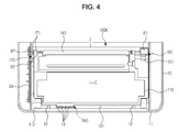
- FIG. 4 is a plan view illustrating a portion of a main body of the image forming apparatus and the developing device. Although only the developing device 100K storing black developer will be described herein, the following description can actually be applied to the other developing devices 100C, 100M and 100Y in a same manner.
- the developing device 100K includes a driving force reception unit 160 to receive a driving force from the main body 10 of the image forming apparatus 1 ( FIG. 2 ), and a power reception unit 170 transmitted with an electric power from the main body 10.
- the driving force reception unit 160 and the power reception unit 170 are disposed opposite to each other with respect to a width direction W of the developing device 100K.
- the driving force reception unit 160 is supplied with the driving force required for operations of the developing roller 140, the supplying roller 130 ( FIG. 2 ) and the agitating member 150 ( FIG. 2 ).
- the driving force reception unit 160 is disposed at one side of a front end of the developing device 100K with respect to the mounting direction A of the developing device 100K.
- the driving force reception unit 160 includes a connecting gear 161 rotatably mounted to the developing device housing 110, and a developing roller driving gear 162 meshed with the connecting gear 161.
- the main body 10 of the image forming apparatus includes a power transmission gear 81 to transmit a driving power to the developing device 100K.
- the connecting gear 161 of the developing device 100K is meshed with the power transmission gear 81 as illustrated in FIG. 4 .
- the power transmission gear 81 is rotated by a driving motor (not illustrated) mounted in the main body 10.
- the connecting gear 161, rotating in mesh with the power transmission gear 81 transmits the driving power to the developing roller driving gear 162 to rotate the developing roller 140.
- the connecting gear 161 transmits the driving power to the supplying roller 130 ( FIG. 2 ) and the agitating member 150 ( FIG. 2 ), thereby rotating the supplying roller 130 and the agitating member 150.
- the power reception unit 170 is applied with the electric power required to electrify the developing roller 140, the supplying roller 130 or the restriction member 111. Therefore, the power reception unit 170 is disposed at an other side of the front end of the developing device 100K.
- the power reception unit 170 includes first electric contact points 171 exposed to a lateral side of the developing device 100K.
- a circuit board 90 is provided at the main body 10 of the image forming apparatus 1, adjoining the power reception unit 170. Additionally, the main body 10 includes second electric contact points 82 arranged corresponding to the first electric contact points 171. The second electric contact points 82 are electrically connected with the circuit board 90.
- the first electric contact points 171 of the developing device 100K are connected to the second electric contact points 82 of the main body 10 as illustrated in FIG. 4 . Accordingly, the electric power applied from the circuit board 90 can be transmitted to the developing device 100K through the second and the first electric contact points 82 and 171.
- the transferring device 50 includes an intermediate transfer belt 51, a first transfer roller 52 and a second transfer roller 53.
- the intermediate transfer belt 51 runs at a same velocity as a linear velocity of the photoconductive medium 40, as being supported by supporting rollers 54 and 55.
- the first transfer roller 52 faces the photoconductive medium 40 with the intermediate transfer belt 51 disposed therebetween, and transfers the visible image formed on the photoconductive medium 40 to the intermediate transfer belt 51.
- the second transfer roller 53 faces the supporting roller 55 with the intermediate transfer belt 51 disposed therebetween. While the visible image is being transferred from the photoconductive medium 40 to the intermediate transfer belt 51, the second transfer roller 53 is distanced away from the intermediate transfer belt 51. Alternatively, after the image of the photoconductive medium 40 is completely transferred to the intermediate transfer belt 51, the second transfer roller 53 is brought into contact with the intermediate transfer belt 51 by a predetermined pressure. When the contact between the second transfer roller 53 and the intermediate transfer belt 51 is achieved, the visible image is transferred from the intermediate transfer belt 51 to the printing medium.
- the fixing device 60 includes a heating roller 61 including a heat source, and a pressing roller 62 mounted opposite to the heating roller 61. As the printing medium passes through between the heating roller 61 and the pressing roller 62, the image is fixed to the printing medium by heat transmitted from the heating roller 61 and pressure exerted between the heating roller 61 and the pressing roller 62.
- the printing medium discharging device 70 including a discharging roller 71 and a backup roller 72, discharges the printing medium passed through the fixing device 60 to the outside of the main body 10.
- the operation of the above-structured image forming apparatus will be briefly described.
- the surface of the photoconductive medium 40 is electrified uniformly by the electrifying roller 42.
- a light corresponding to image information on any one color, for example, information on a yellow image is projected by the laser scanning device 30. Accordingly, an electrostatic latent image corresponding to the yellow image is formed on the photoconductive medium 40.
- the developing bias is applied to the developing roller 140 of the yellow developing device 100Y Accordingly, the yellow developer is attached to the electrostatic latent image, thereby forming a visible image of yellow color on the photoconductive medium 40.
- the visible image is transferred to the intermediate transfer belt 51 through the first transfer roller 52.
- the laser scanning device 30 After transferring of the yellow image for one page is completed, the laser scanning device 30 now projects a light corresponding to image information on another color, for example, information on a magenta image to the photoconductive medium 40, thereby forming an electrostatic latent image corresponding to the magenta image.
- the magenta developing device 100M forms a visible image of magenta color by supplying magenta developer to the electrostatic latent image.
- the magenta visible image formed on the photoconductive medium 40 is transferred to the intermediate transfer belt through the first transfer roller 52. At this time, the magenta visible image is superposed on the yellow visible image previously transferred.
- a full-color image wherein the yellow, magenta, cyan and black images are overlapped is formed on the intermediate transfer belt 51.
- the full-color image is transferred to the printing medium while the printing medium is passing through between the intermediate transfer belt 51 and the second transfer belt 53. Then, the printing medium is passed through the fixing device 60 and the discharging device 70, thereby being discharged out of the main body 10.
- the developers stored in the respective developing devices 100K, 100C, 100M and 100Y are consumed and life of the parts such as the developing roller 140 and the supplying roller 130 is gradually exhausted.
- the user needs to be aware of various information on the developing devices 100K, 100C, 100M and 100Y so as to timely replace the developing devices 100K, 100C, 100M and 100Y.
- the developing devices 100K, 100C, 100M and 100Y each include a memory unit 180 to store various usage information.
- the memory unit 180 may store information on individual operation history of the developing devices 100K, 100C, 100M and 100Y, a residual quantity of the developer and a remaining life span of the component parts such as the developing roller 140 and the supplying roller 130.
- the memory unit 180 includes terminals 181 for electric connection with a power unit provided to the main body 10, for example, the circuit board 90.
- the main body 10 includes terminal contact points 13 for contact with the terminals 181.
- the terminal contact points 13 are formed at the main body cover 11 disposed at the rear portion of the developing devices 100K, 100C, 100M and 100Y, and electrically connected with the circuit board 90 through a harness (not illustrated).
- the terminal contact points 13 may have a predetermined elasticity for efficient contact with the terminals 181.
- the memory unit 180 of the black developing device 100K will be described as an example. However, the following description can actually be applied to the memory units 180 of the other developing devices 100C, 100M and 100Y in the same manner.
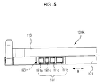
- FIG. 5 illustrates a rear side of the developing device according to an embodiment of the present general inventive concept.
- the memory unit 180 is disposed at a rear end of the developing device 100K with respect to the direction A to mount the developing device 100K to the main body 10.
- the terminals 181 of the memory unit 180 are exposed to the outside through a rear end 101 of the developing device 100K.
- the memory unit 180 When the memory unit 180 is mounted in this way, the memory unit 180 is disposed at a distance from the fixing device 60, the photoconductive medium 40 and the developing roller 140 as illustrated in FIG. 2 . As a result, damage of the memory unit 180 by high heat can be prevented and contamination of the terminals 181 by the developer scattering about can also be prevented. Furthermore, since the terminals 181 of the memory unit 180 are at the rear side of the developing device 100K, interference with other parts is reduced. Therefore, the terminals 181 will not be damaged while mounting and separating the developing device 100K with respect to the main body 10.
- the position of the memory unit 180 is biased to one side from a middle C of a width of the developing device 100K. More specifically, the memory unit 180 is biased to the left in FIG. 4 and FIG. 5 such that the terminals 181 are disposed relatively close to the power reception unit 170 compared with the driving force reception unit 160.
- the memory unit 180 When the memory unit 180 is thus disposed relatively far from the driving force reception unit 160, the memory unit 180 would not be too affected by the vibration generated during transmission of the driving force from the main body 10 to the driving force reception unit 160. Accordingly, the connection between the terminals 181 and the terminal contact points 13 can be stably maintained.
- the memory unit 180 By disposing the memory unit 180 relatively close to the power reception unit 170, the position of the terminal contact points 13 of the main body cover 11 is biased toward the circuit board 90. Therefore, a length of the harness connecting the terminal contact points 13 can be reduced. As a result, cost for the harness can be saved while reducing adverse effects of electromagnetic waves generated around the harness.
- the terminals 181 of the memory unit 180 include first through fourth terminals 181 a, 181 b, 181c and 181d arranged in the width direction W of the developing device 100K.
- the first terminal 181 a is a data communication terminal for information exchange with a control unit (not illustrated) provided at the main body 10 of the image forming apparatus.
- the control unit (not illustrated) of the image forming apparatus reads necessary information from the memory unit 180 or stores new information in the memory unit 180 through the first terminal 181 a.
- the second terminal 181b is a grounding terminal to ground the memory unit 180.
- the third terminal 181c is a power terminal to apply the electric power to the memory unit 180.
- the fourth terminal 181d is a clock terminal to transmit clock signals to the memory unit 180.
- the first terminal 181 a is disposed farthest from the driving force reception unit 160 of the developing device 100K. As illustrated in FIG. 4 , when the driving force reception unit 160 is on the right of the developing device 100K, the first terminal 181a is at a leftmost position among the four terminals.
- the reason of disposing the first terminal 181 a as far as possible from the driving force reception unit 160 is to restrain a data transmission error caused by the vibration from the driving force reception unit 160.
- the second terminal 181 b may be at a closest position to the driving force reception unit 160. That is, when the driving force reception unit 160 is on the right of the developing device 100K as illustrated in FIG. 4 , the second terminal 181b is at a rightmost position among the four terminals.
- the second terminal 181b which is the grounding terminal, contacts the terminal contact point 13 of the main body cover 11 without a function of transceiving certain information or signals. Therefore, although the second terminal 181 b is most affected by the vibration since being disposed close to the driving force reception unit 160, a chance of an operational error by the poor connection would be reduced.
- the second terminal 181 b may have a larger area than other terminals 181 a, 181 c and 181 d.
- the memory unit is disposed at a position subject to less vibration transmitted from a driving force reception unit of the developing device.
- terminals of the memory unit are disposed at proper positions in consideration of a respective function of each terminal so that an operational error caused by poor connection of the terminals can be minimized.
- contact points of terminals connected to a memory unit are disposed near a circuit board that supplies an electric power to a developing device, a length of a harness connecting the contact points with the circuit board can be reduced. As a result, cost of parts can be saved while restraining adverse effects of electromagnetic waves generated around the harness.
- the present general inventive concept is not limited to the color image forming apparatus. That is, the present general inventive concept is also applicable to a black-and-white image forming apparatus having a single developing device.
Priority Applications (8)
| Application Number | Priority Date | Filing Date | Title |
|---|---|---|---|
| PL14166674T PL2762981T3 (pl) | 2007-09-11 | 2008-07-24 | Urządzenie wywołujące, jego zespół pamięci i aparat do tworzenia obrazu |
| PL19171653T PL3540519T3 (pl) | 2007-09-11 | 2008-07-24 | Urządzenie wywołujące i urządzenie do tworzenia obrazów |
| EP11180248.4A EP2397914B2 (fr) | 2007-09-11 | 2008-07-24 | Dispositif de développement et appareil de formation d'image |
| PL11157138T PL2325701T3 (pl) | 2007-09-11 | 2008-07-24 | Urządzenie wywołujące, urządzenie do generowania obrazu i zastosowanie urządzenia wywołującego |
| DK11180248.4T DK2397914T4 (en) | 2007-09-11 | 2008-07-24 | Developer and imaging apparatus |
| EP14166674.3A EP2762981B1 (fr) | 2007-09-11 | 2008-07-24 | Dispositif de développement, son unité mémoire et appareil de formation d'image |
| EP19171653.9A EP3540519B1 (fr) | 2007-09-11 | 2008-07-24 | Dispositif de développement et appareil de formation d'image |
| PL11180248T PL2397914T5 (pl) | 2007-09-11 | 2008-07-24 | Urządzenie do wywoływania oraz przyrząd do generowania obrazu |
Applications Claiming Priority (3)
| Application Number | Priority Date | Filing Date | Title |
|---|---|---|---|
| KR1020070091999A KR20090026916A (ko) | 2007-09-11 | 2007-09-11 | 동력전달유닛과 이를 채용한 현상장치 및 화상형성기기 |
| KR1020080018969A KR100863252B1 (ko) | 2008-02-29 | 2008-02-29 | 현상기와 그 메모리 유닛 및 화상형성장치 |
| EP08161123.8A EP2037327B2 (fr) | 2007-09-11 | 2008-07-24 | Appareil de formation d'image et l'utilisation d' un dispositif de développement |
Related Parent Applications (2)
| Application Number | Title | Priority Date | Filing Date |
|---|---|---|---|
| EP08161123.8A Division-Into EP2037327B2 (fr) | 2007-09-11 | 2008-07-24 | Appareil de formation d'image et l'utilisation d' un dispositif de développement |
| EP08161123.8 Division | 2008-07-24 |
Related Child Applications (4)
| Application Number | Title | Priority Date | Filing Date |
|---|---|---|---|
| EP11180248.4A Division EP2397914B2 (fr) | 2007-09-11 | 2008-07-24 | Dispositif de développement et appareil de formation d'image |
| EP19171653.9A Division EP3540519B1 (fr) | 2007-09-11 | 2008-07-24 | Dispositif de développement et appareil de formation d'image |
| EP14166674.3A Division EP2762981B1 (fr) | 2007-09-11 | 2008-07-24 | Dispositif de développement, son unité mémoire et appareil de formation d'image |
| EP11180248.4 Division-Into | 2011-09-06 |
Publications (2)
| Publication Number | Publication Date |
|---|---|
| EP2325701A1 true EP2325701A1 (fr) | 2011-05-25 |
| EP2325701B1 EP2325701B1 (fr) | 2011-10-19 |
Family
ID=40091393
Family Applications (6)
| Application Number | Title | Priority Date | Filing Date |
|---|---|---|---|
| EP08161123.8A Active EP2037327B2 (fr) | 2007-09-11 | 2008-07-24 | Appareil de formation d'image et l'utilisation d' un dispositif de développement |
| EP19171653.9A Active EP3540519B1 (fr) | 2007-09-11 | 2008-07-24 | Dispositif de développement et appareil de formation d'image |
| EP10174269A Active EP2256559B1 (fr) | 2007-09-11 | 2008-07-24 | Dispositif de développement et appareil de formation d'image |
| EP11180248.4A Active EP2397914B2 (fr) | 2007-09-11 | 2008-07-24 | Dispositif de développement et appareil de formation d'image |
| EP14166674.3A Active EP2762981B1 (fr) | 2007-09-11 | 2008-07-24 | Dispositif de développement, son unité mémoire et appareil de formation d'image |
| EP11157138A Active EP2325701B1 (fr) | 2007-09-11 | 2008-07-24 | Dispositif de développement, appareil de formation d'image et emploi du dispositif de développement |
Family Applications Before (5)
| Application Number | Title | Priority Date | Filing Date |
|---|---|---|---|
| EP08161123.8A Active EP2037327B2 (fr) | 2007-09-11 | 2008-07-24 | Appareil de formation d'image et l'utilisation d' un dispositif de développement |
| EP19171653.9A Active EP3540519B1 (fr) | 2007-09-11 | 2008-07-24 | Dispositif de développement et appareil de formation d'image |
| EP10174269A Active EP2256559B1 (fr) | 2007-09-11 | 2008-07-24 | Dispositif de développement et appareil de formation d'image |
| EP11180248.4A Active EP2397914B2 (fr) | 2007-09-11 | 2008-07-24 | Dispositif de développement et appareil de formation d'image |
| EP14166674.3A Active EP2762981B1 (fr) | 2007-09-11 | 2008-07-24 | Dispositif de développement, son unité mémoire et appareil de formation d'image |
Country Status (11)
| Country | Link |
|---|---|
| US (3) | US7742717B2 (fr) |
| EP (6) | EP2037327B2 (fr) |
| AT (3) | ATE549667T1 (fr) |
| BR (1) | BRPI0805241A2 (fr) |
| DE (1) | DE202008018442U1 (fr) |
| DK (1) | DK2397914T4 (fr) |
| ES (6) | ES2870721T3 (fr) |
| HU (1) | HUE044619T2 (fr) |
| PL (6) | PL2256559T3 (fr) |
| PT (1) | PT2397914E (fr) |
| RU (1) | RU2391690C2 (fr) |
Families Citing this family (16)
| Publication number | Priority date | Publication date | Assignee | Title |
|---|---|---|---|---|
| KR101590336B1 (ko) * | 2008-04-01 | 2016-02-01 | 삼성전자주식회사 | 화상형성장치 및 그 제어방법 |
| CN104076672B (zh) | 2010-06-11 | 2020-10-09 | 株式会社理光 | 信息存储装置、可拆卸装置、显影剂容器和成像设备 |
| JP5779572B2 (ja) * | 2012-12-05 | 2015-09-16 | 京セラドキュメントソリューションズ株式会社 | 支持ユニット、およびこれを備えた画像形成装置 |
| US9104169B2 (en) * | 2013-01-24 | 2015-08-11 | Samsung Electronics Co., Ltd. | Electrophotographic image forming apparatus |
| CN203365924U (zh) * | 2013-01-24 | 2013-12-25 | 三星电子株式会社 | 电子照相图像形成设备及显影盒 |
| US9195165B2 (en) * | 2014-01-06 | 2015-11-24 | Brother Kogyo Kabushiki Kaisha | Developing cartridge and process cartridge |
| JP6493738B2 (ja) * | 2014-12-17 | 2019-04-03 | 株式会社リコー | 防塵カバー、画像形成装置 |
| US9996052B2 (en) * | 2016-02-10 | 2018-06-12 | Canon Kabushiki Kaisha | Cartridge capable of being inserted in an apparatus main body of an image forming apparatus |
| JP6658158B2 (ja) * | 2016-03-18 | 2020-03-04 | ブラザー工業株式会社 | 画像形成装置 |
| JP6859647B2 (ja) * | 2016-09-30 | 2021-04-14 | ブラザー工業株式会社 | ドラムカートリッジ |
| JP6764816B2 (ja) * | 2017-03-24 | 2020-10-07 | 株式会社沖データ | 現像ユニット、画像形成ユニットおよび画像形成装置 |
| JP2019045595A (ja) * | 2017-08-31 | 2019-03-22 | 京セラドキュメントソリューションズ株式会社 | トナー容器、画像形成装置 |
| JP7151106B2 (ja) * | 2018-03-12 | 2022-10-12 | ブラザー工業株式会社 | ドラムカートリッジおよび画像形成装置 |
| JP7224904B2 (ja) * | 2018-12-26 | 2023-02-20 | キヤノン株式会社 | 画像形成装置で用いるカートリッジ |
| JP7306073B2 (ja) * | 2019-06-06 | 2023-07-11 | ブラザー工業株式会社 | 転写ベルトユニットおよび画像形成装置 |
| JP7419065B2 (ja) | 2019-12-27 | 2024-01-22 | キヤノン株式会社 | 画像形成装置 |
Citations (7)
| Publication number | Priority date | Publication date | Assignee | Title |
|---|---|---|---|---|
| US5204713A (en) * | 1990-08-24 | 1993-04-20 | Tokyo Electric Co., Ltd. | Electrophotographic apparatus |
| JP2003195723A (ja) * | 2001-12-28 | 2003-07-09 | Canon Inc | 画像形成装置 |
| JP2003255698A (ja) * | 2002-03-06 | 2003-09-10 | Seiko Epson Corp | コネクタ、現像カートリッジ及び画像形成装置 |
| US20030170042A1 (en) * | 2002-02-19 | 2003-09-11 | Seiko Epson Corporation | Connector, development cartridge, and image forming apparatus |
| US20050078978A1 (en) * | 2003-10-08 | 2005-04-14 | Canon Kabushiki Kaisha | Process cartridge and electrophotographic image forming apparatus |
| US20060024080A1 (en) * | 2004-07-30 | 2006-02-02 | Canon Kabushiki Kaisha | Process cartridge and electrophotographic image forming apparatus |
| US20070189781A1 (en) * | 2006-02-14 | 2007-08-16 | Konica Minolta Business Technologies, Inc. | Consumable cartridge for image forming apparatus and image forming apparatus |
Family Cites Families (45)
| Publication number | Priority date | Publication date | Assignee | Title |
|---|---|---|---|---|
| US5272503A (en) † | 1992-09-02 | 1993-12-21 | Xerox Corporation | Replaceable sub-assemblies for electrostatographic reproducing machines |
| JP3507571B2 (ja) * | 1995-03-06 | 2004-03-15 | シャープ株式会社 | 画像形成装置の現像装置 |
| JP3359245B2 (ja) * | 1995-10-25 | 2002-12-24 | キヤノン株式会社 | プロセスカートリッジ及び電子写真画像形成装置 |
| JPH09213407A (ja) * | 1996-01-31 | 1997-08-15 | Canon Inc | コネクタ及びユニット及びプロセスカートリッジ及び電子写真画像形成装置 |
| JP3715723B2 (ja) * | 1996-07-24 | 2005-11-16 | キヤノン株式会社 | カートリッジコネクタ、プロセスカートリッジ及び電子写真画像形成装置 |
| JP3332818B2 (ja) * | 1996-08-29 | 2002-10-07 | キヤノン株式会社 | プロセスカートリッジ及び電子写真画像形成装置及び接続端子の接続方法 |
| JPH11242371A (ja) * | 1997-10-31 | 1999-09-07 | Canon Inc | コネクタ及びユニット及びプロセスカ―トリッジ及び電子写真画像形成装置 |
| US6157792A (en) * | 1998-03-31 | 2000-12-05 | Canon Kabushiki Kaisha | Electrophotographic apparatus having plural image forming modes, and a process cartridge applied to such electrophotographic apparatus |
| JP3697090B2 (ja) * | 1998-10-26 | 2005-09-21 | キヤノン株式会社 | 電子写真画像形成装置 |
| JP3447595B2 (ja) * | 1998-12-22 | 2003-09-16 | シャープ株式会社 | 画像形成装置 |
| JP2002202698A (ja) | 2000-12-28 | 2002-07-19 | Sharp Corp | 保守安全装置 |
| JP3774691B2 (ja) * | 2001-10-01 | 2006-05-17 | キヤノン株式会社 | 電子写真画像形成装置 |
| CN1262892C (zh) | 2002-04-09 | 2006-07-05 | 佳能株式会社 | 处理盒,用于处理盒的存储介质,成像设备和成像控制系统 |
| JP4194298B2 (ja) * | 2002-05-17 | 2008-12-10 | キヤノン株式会社 | 情報記憶媒体、ユニット、プロセスカートリッジ、現像カートリッジおよび電子写真画像形成装置 |
| KR100484198B1 (ko) † | 2002-06-25 | 2005-04-20 | 삼성전자주식회사 | 전자사진방식 화상형성장치의 현상유닛 및 그를 채용한 전자사진방식 화상형성장치 |
| JP4585746B2 (ja) † | 2002-06-25 | 2010-11-24 | 三星電子株式会社 | 電子写真方式の画像形成装置の現像ユニット及びそれを採用した電子写真方式の画像形成装置 |
| KR100497489B1 (ko) † | 2003-02-06 | 2005-07-01 | 삼성전자주식회사 | 현상유니트 |
| KR100547128B1 (ko) † | 2003-07-04 | 2006-01-26 | 삼성전자주식회사 | 전자사진방식 인쇄기 |
| KR100547131B1 (ko) † | 2003-07-04 | 2006-01-26 | 삼성전자주식회사 | 전자사진방식 인쇄기 |
| KR100553897B1 (ko) * | 2003-10-31 | 2006-02-24 | 삼성전자주식회사 | 메모리를 이용한 화상형성장치의 소모품 관리 장치 |
| US7369783B2 (en) * | 2003-10-31 | 2008-05-06 | Ricoh Company, Limited | Image forming apparatus, process cartridge, and development unit |
| US20050254835A1 (en) * | 2004-05-17 | 2005-11-17 | Fuji Xerox Co., Ltd. | Image formation apparatus to which replacement unit is attached and image formation system |
| JP4766365B2 (ja) * | 2004-05-17 | 2011-09-07 | 富士ゼロックス株式会社 | 交換ユニットが装着された画像形成装置 |
| JP5002120B2 (ja) * | 2004-05-17 | 2012-08-15 | 富士ゼロックス株式会社 | 交換ユニットが装着された画像形成装置及び画像形成システム |
| JP2005338392A (ja) | 2004-05-26 | 2005-12-08 | Canon Inc | 画像形成装置 |
| KR100605356B1 (ko) * | 2004-07-15 | 2006-07-31 | 삼성전자주식회사 | 화상형성장치 |
| JP4110144B2 (ja) * | 2004-09-17 | 2008-07-02 | キヤノン株式会社 | 電子写真画像形成装置 |
| KR100584617B1 (ko) † | 2005-01-20 | 2006-05-30 | 삼성전자주식회사 | 현상카트리지 및 이를 채용한 전자사진방식 화상형성장치 |
| JP4378311B2 (ja) | 2005-04-05 | 2009-12-02 | キヤノン株式会社 | 画像形成装置 |
| KR100677576B1 (ko) † | 2005-04-22 | 2007-02-02 | 삼성전자주식회사 | 전자사진방식 화상형성장치 |
| KR100633097B1 (ko) † | 2005-07-22 | 2006-10-11 | 삼성전자주식회사 | 화상형성 프로세스모듈 및 그것을 구비한 화상형성장치 |
| JP4929671B2 (ja) | 2005-10-19 | 2012-05-09 | 富士ゼロックス株式会社 | 画像形成装置及びその制御方法 |
| KR101041080B1 (ko) † | 2006-10-13 | 2011-06-13 | 삼성전자주식회사 | 현상기용 토너감지 센서의 에러 인식장치 및 그 방법 |
| JP4280772B2 (ja) † | 2006-12-28 | 2009-06-17 | キヤノン株式会社 | プロセスカートリッジ及び電子写真画像形成装置 |
| US7912403B2 (en) * | 2007-01-15 | 2011-03-22 | Samsung Electronics Co., Ltd. | Image forming apparatus with frame and pressing member |
| US8005392B2 (en) * | 2007-02-20 | 2011-08-23 | Brother Kogyo Kabushiki Kaisha | Image forming device with pressing members, process cartridge, and developer cartridge |
| KR100950492B1 (ko) † | 2007-03-15 | 2010-03-31 | 삼성전자주식회사 | 현상기, 이를 구비한 화상형성장치, 및 현상기의 탈착방법 |
| KR100888686B1 (ko) * | 2007-03-15 | 2009-03-13 | 삼성전자주식회사 | 현상기, 화상형성장치 및 현상기 장착방법과 탈착방법 |
| US7321739B1 (en) * | 2007-04-30 | 2008-01-22 | Lexmark International, Inc. | Cartridge with a handle for use with an image forming device |
| KR20090026916A (ko) | 2007-09-11 | 2009-03-16 | 삼성전자주식회사 | 동력전달유닛과 이를 채용한 현상장치 및 화상형성기기 |
| KR100889820B1 (ko) * | 2007-09-19 | 2009-03-20 | 삼성전자주식회사 | 현상장치 및 이를 구비하는 화상형성장치 |
| KR100933290B1 (ko) * | 2008-02-22 | 2009-12-22 | 삼성전자주식회사 | 메모리부, 현상제카트리지, 현상장치 및 이들을 포함하는화상형성장치 |
| KR101590336B1 (ko) * | 2008-04-01 | 2016-02-01 | 삼성전자주식회사 | 화상형성장치 및 그 제어방법 |
| KR101502905B1 (ko) * | 2008-11-26 | 2015-03-17 | 삼성전자주식회사 | 온도센서 내장형 현상기가 채용된 화상형성장치 및 그 제어방법 |
| KR101720185B1 (ko) * | 2009-10-15 | 2017-03-28 | 에스프린팅솔루션 주식회사 | 화상형성장치 |
-
2008
- 2008-07-15 US US12/173,254 patent/US7742717B2/en not_active Ceased
- 2008-07-22 RU RU2008130350/28A patent/RU2391690C2/ru active
- 2008-07-24 PL PL10174269T patent/PL2256559T3/pl unknown
- 2008-07-24 ES ES19171653T patent/ES2870721T3/es active Active
- 2008-07-24 ES ES11157138T patent/ES2375189T3/es active Active
- 2008-07-24 ES ES11180248.4T patent/ES2495665T5/es active Active
- 2008-07-24 PL PL11180248T patent/PL2397914T5/pl unknown
- 2008-07-24 PL PL14166674T patent/PL2762981T3/pl unknown
- 2008-07-24 ES ES10174269T patent/ES2383879T3/es active Active
- 2008-07-24 AT AT10174269T patent/ATE549667T1/de active
- 2008-07-24 AT AT11157138T patent/ATE529783T1/de not_active IP Right Cessation
- 2008-07-24 EP EP08161123.8A patent/EP2037327B2/fr active Active
- 2008-07-24 EP EP19171653.9A patent/EP3540519B1/fr active Active
- 2008-07-24 DE DE202008018442U patent/DE202008018442U1/de not_active Expired - Lifetime
- 2008-07-24 DK DK11180248.4T patent/DK2397914T4/en active
- 2008-07-24 EP EP10174269A patent/EP2256559B1/fr active Active
- 2008-07-24 ES ES14166674T patent/ES2733762T3/es active Active
- 2008-07-24 HU HUE14166674 patent/HUE044619T2/hu unknown
- 2008-07-24 AT AT08161123T patent/ATE523814T1/de not_active IP Right Cessation
- 2008-07-24 EP EP11180248.4A patent/EP2397914B2/fr active Active
- 2008-07-24 EP EP14166674.3A patent/EP2762981B1/fr active Active
- 2008-07-24 PL PL19171653T patent/PL3540519T3/pl unknown
- 2008-07-24 PL PL08161123T patent/PL2037327T5/pl unknown
- 2008-07-24 EP EP11157138A patent/EP2325701B1/fr active Active
- 2008-07-24 PL PL11157138T patent/PL2325701T3/pl unknown
- 2008-07-24 ES ES08161123T patent/ES2373822T5/es active Active
- 2008-07-24 PT PT111802484T patent/PT2397914E/pt unknown
- 2008-07-31 BR BRPI0805241-7A patent/BRPI0805241A2/pt active IP Right Grant
-
2010
- 2010-05-12 US US12/778,416 patent/US8126353B2/en active Active
-
2015
- 2015-03-13 US US14/657,486 patent/USRE46519E1/en active Active
Patent Citations (7)
| Publication number | Priority date | Publication date | Assignee | Title |
|---|---|---|---|---|
| US5204713A (en) * | 1990-08-24 | 1993-04-20 | Tokyo Electric Co., Ltd. | Electrophotographic apparatus |
| JP2003195723A (ja) * | 2001-12-28 | 2003-07-09 | Canon Inc | 画像形成装置 |
| US20030170042A1 (en) * | 2002-02-19 | 2003-09-11 | Seiko Epson Corporation | Connector, development cartridge, and image forming apparatus |
| JP2003255698A (ja) * | 2002-03-06 | 2003-09-10 | Seiko Epson Corp | コネクタ、現像カートリッジ及び画像形成装置 |
| US20050078978A1 (en) * | 2003-10-08 | 2005-04-14 | Canon Kabushiki Kaisha | Process cartridge and electrophotographic image forming apparatus |
| US20060024080A1 (en) * | 2004-07-30 | 2006-02-02 | Canon Kabushiki Kaisha | Process cartridge and electrophotographic image forming apparatus |
| US20070189781A1 (en) * | 2006-02-14 | 2007-08-16 | Konica Minolta Business Technologies, Inc. | Consumable cartridge for image forming apparatus and image forming apparatus |
Also Published As
Similar Documents
| Publication | Publication Date | Title |
|---|---|---|
| EP3540519B1 (fr) | Dispositif de développement et appareil de formation d'image | |
| JP4289375B2 (ja) | 画像形成装置 | |
| US8112011B2 (en) | Image forming apparatus | |
| US7986898B2 (en) | Image forming apparatus with contacts for memory chips | |
| US8023854B2 (en) | Image forming apparatus having power supplying path | |
| US20010016123A1 (en) | Electrophotographic image forming apparatus | |
| EP1705526A1 (fr) | Appareil de generation d'image pouvant afficher une quantite totale restante d'agent de developpement pourvu dans un mode d'impression monochrome | |
| US20220004144A1 (en) | Cartridge, image forming apparatus, and method for manufacturing cartridge | |
| JP2005227712A (ja) | 画像形成装置 | |
| JP2018155777A (ja) | 画像形成装置及び現像ユニット | |
| JP2022052274A (ja) | 基板ユニット、着脱ユニット、及び、画像形成装置 | |
| KR100863252B1 (ko) | 현상기와 그 메모리 유닛 및 화상형성장치 | |
| JP2009205082A (ja) | イメージングカートリッジ及び画像形成装置 | |
| US20220088950A1 (en) | Circuit board unit, attachment unit, and image forming apparatus | |
| JP3778178B2 (ja) | 画像形成装置、及び、画像形成システム | |
| JP2005031441A (ja) | 画像形成装置、及び、画像形成システム |
Legal Events
| Date | Code | Title | Description |
|---|---|---|---|
| PUAI | Public reference made under article 153(3) epc to a published international application that has entered the european phase |
Free format text: ORIGINAL CODE: 0009012 |
|
| 17P | Request for examination filed |
Effective date: 20110307 |
|
| AC | Divisional application: reference to earlier application |
Ref document number: 2037327 Country of ref document: EP Kind code of ref document: P |
|
| AK | Designated contracting states |
Kind code of ref document: A1 Designated state(s): AT BE BG CH CY CZ DE DK EE ES FI FR GB GR HR HU IE IS IT LI LT LU LV MC MT NL NO PL PT RO SE SI SK TR |
|
| GRAP | Despatch of communication of intention to grant a patent |
Free format text: ORIGINAL CODE: EPIDOSNIGR1 |
|
| GRAS | Grant fee paid |
Free format text: ORIGINAL CODE: EPIDOSNIGR3 |
|
| RIC1 | Information provided on ipc code assigned before grant |
Ipc: G03G 15/00 20060101AFI20110803BHEP Ipc: G03G 15/08 20060101ALI20110803BHEP |
|
| RTI1 | Title (correction) |
Free format text: DEVELOPING DEVICE, IMAGE FORMING APPARATUS AND USE OF THE DEVELOPING DEVICE |
|
| GRAA | (expected) grant |
Free format text: ORIGINAL CODE: 0009210 |
|
| AC | Divisional application: reference to earlier application |
Ref document number: 2037327 Country of ref document: EP Kind code of ref document: P |
|
| AK | Designated contracting states |
Kind code of ref document: B1 Designated state(s): AT BE BG CH CY CZ DE DK EE ES FI FR GB GR HR HU IE IS IT LI LT LU LV MC MT NL NO PL PT RO SE SI SK TR |
|
| REG | Reference to a national code |
Ref country code: GB Ref legal event code: FG4D |
|
| REG | Reference to a national code |
Ref country code: CH Ref legal event code: EP |
|
| REG | Reference to a national code |
Ref country code: IE Ref legal event code: FG4D |
|
| REG | Reference to a national code |
Ref country code: DE Ref legal event code: R096 Ref document number: 602008010686 Country of ref document: DE Effective date: 20111229 |
|
| REG | Reference to a national code |
Ref country code: SE Ref legal event code: TRGR |
|
| REG | Reference to a national code |
Ref country code: NL Ref legal event code: T3 |
|
| REG | Reference to a national code |
Ref country code: ES Ref legal event code: FG2A Ref document number: 2375189 Country of ref document: ES Kind code of ref document: T3 Effective date: 20120227 |
|
| LTIE | Lt: invalidation of european patent or patent extension |
Effective date: 20111019 |
|
| REG | Reference to a national code |
Ref country code: PL Ref legal event code: T3 |
|
| REG | Reference to a national code |
Ref country code: AT Ref legal event code: MK05 Ref document number: 529783 Country of ref document: AT Kind code of ref document: T Effective date: 20111019 |
|
| PG25 | Lapsed in a contracting state [announced via postgrant information from national office to epo] |
Ref country code: IS Free format text: LAPSE BECAUSE OF FAILURE TO SUBMIT A TRANSLATION OF THE DESCRIPTION OR TO PAY THE FEE WITHIN THE PRESCRIBED TIME-LIMIT Effective date: 20120219 Ref country code: BE Free format text: LAPSE BECAUSE OF FAILURE TO SUBMIT A TRANSLATION OF THE DESCRIPTION OR TO PAY THE FEE WITHIN THE PRESCRIBED TIME-LIMIT Effective date: 20111019 Ref country code: LT Free format text: LAPSE BECAUSE OF FAILURE TO SUBMIT A TRANSLATION OF THE DESCRIPTION OR TO PAY THE FEE WITHIN THE PRESCRIBED TIME-LIMIT Effective date: 20111019 Ref country code: NO Free format text: LAPSE BECAUSE OF FAILURE TO SUBMIT A TRANSLATION OF THE DESCRIPTION OR TO PAY THE FEE WITHIN THE PRESCRIBED TIME-LIMIT Effective date: 20120119 |
|
| PG25 | Lapsed in a contracting state [announced via postgrant information from national office to epo] |
Ref country code: GR Free format text: LAPSE BECAUSE OF FAILURE TO SUBMIT A TRANSLATION OF THE DESCRIPTION OR TO PAY THE FEE WITHIN THE PRESCRIBED TIME-LIMIT Effective date: 20120120 Ref country code: PT Free format text: LAPSE BECAUSE OF FAILURE TO SUBMIT A TRANSLATION OF THE DESCRIPTION OR TO PAY THE FEE WITHIN THE PRESCRIBED TIME-LIMIT Effective date: 20120220 Ref country code: LV Free format text: LAPSE BECAUSE OF FAILURE TO SUBMIT A TRANSLATION OF THE DESCRIPTION OR TO PAY THE FEE WITHIN THE PRESCRIBED TIME-LIMIT Effective date: 20111019 Ref country code: HR Free format text: LAPSE BECAUSE OF FAILURE TO SUBMIT A TRANSLATION OF THE DESCRIPTION OR TO PAY THE FEE WITHIN THE PRESCRIBED TIME-LIMIT Effective date: 20111019 Ref country code: SI Free format text: LAPSE BECAUSE OF FAILURE TO SUBMIT A TRANSLATION OF THE DESCRIPTION OR TO PAY THE FEE WITHIN THE PRESCRIBED TIME-LIMIT Effective date: 20111019 |
|
| PG25 | Lapsed in a contracting state [announced via postgrant information from national office to epo] |
Ref country code: CY Free format text: LAPSE BECAUSE OF FAILURE TO SUBMIT A TRANSLATION OF THE DESCRIPTION OR TO PAY THE FEE WITHIN THE PRESCRIBED TIME-LIMIT Effective date: 20111019 |
|
| PG25 | Lapsed in a contracting state [announced via postgrant information from national office to epo] |
Ref country code: CZ Free format text: LAPSE BECAUSE OF FAILURE TO SUBMIT A TRANSLATION OF THE DESCRIPTION OR TO PAY THE FEE WITHIN THE PRESCRIBED TIME-LIMIT Effective date: 20111019 Ref country code: SK Free format text: LAPSE BECAUSE OF FAILURE TO SUBMIT A TRANSLATION OF THE DESCRIPTION OR TO PAY THE FEE WITHIN THE PRESCRIBED TIME-LIMIT Effective date: 20111019 Ref country code: DK Free format text: LAPSE BECAUSE OF FAILURE TO SUBMIT A TRANSLATION OF THE DESCRIPTION OR TO PAY THE FEE WITHIN THE PRESCRIBED TIME-LIMIT Effective date: 20111019 Ref country code: EE Free format text: LAPSE BECAUSE OF FAILURE TO SUBMIT A TRANSLATION OF THE DESCRIPTION OR TO PAY THE FEE WITHIN THE PRESCRIBED TIME-LIMIT Effective date: 20111019 Ref country code: BG Free format text: LAPSE BECAUSE OF FAILURE TO SUBMIT A TRANSLATION OF THE DESCRIPTION OR TO PAY THE FEE WITHIN THE PRESCRIBED TIME-LIMIT Effective date: 20120119 |
|
| PLBE | No opposition filed within time limit |
Free format text: ORIGINAL CODE: 0009261 |
|
| STAA | Information on the status of an ep patent application or granted ep patent |
Free format text: STATUS: NO OPPOSITION FILED WITHIN TIME LIMIT |
|
| PG25 | Lapsed in a contracting state [announced via postgrant information from national office to epo] |
Ref country code: RO Free format text: LAPSE BECAUSE OF FAILURE TO SUBMIT A TRANSLATION OF THE DESCRIPTION OR TO PAY THE FEE WITHIN THE PRESCRIBED TIME-LIMIT Effective date: 20111019 |
|
| RAP2 | Party data changed (patent owner data changed or rights of a patent transferred) |
Owner name: SAMSUNG ELECTRONICS CO., LTD. |
|
| 26N | No opposition filed |
Effective date: 20120720 |
|
| REG | Reference to a national code |
Ref country code: DE Ref legal event code: R097 Ref document number: 602008010686 Country of ref document: DE Effective date: 20120720 |
|
| PG25 | Lapsed in a contracting state [announced via postgrant information from national office to epo] |
Ref country code: AT Free format text: LAPSE BECAUSE OF FAILURE TO SUBMIT A TRANSLATION OF THE DESCRIPTION OR TO PAY THE FEE WITHIN THE PRESCRIBED TIME-LIMIT Effective date: 20111019 |
|
| PG25 | Lapsed in a contracting state [announced via postgrant information from national office to epo] |
Ref country code: MC Free format text: LAPSE BECAUSE OF NON-PAYMENT OF DUE FEES Effective date: 20120731 |
|
| REG | Reference to a national code |
Ref country code: IE Ref legal event code: MM4A |
|
| PG25 | Lapsed in a contracting state [announced via postgrant information from national office to epo] |
Ref country code: FI Free format text: LAPSE BECAUSE OF FAILURE TO SUBMIT A TRANSLATION OF THE DESCRIPTION OR TO PAY THE FEE WITHIN THE PRESCRIBED TIME-LIMIT Effective date: 20111019 |
|
| PG25 | Lapsed in a contracting state [announced via postgrant information from national office to epo] |
Ref country code: IE Free format text: LAPSE BECAUSE OF NON-PAYMENT OF DUE FEES Effective date: 20120724 Ref country code: MT Free format text: LAPSE BECAUSE OF FAILURE TO SUBMIT A TRANSLATION OF THE DESCRIPTION OR TO PAY THE FEE WITHIN THE PRESCRIBED TIME-LIMIT Effective date: 20111019 |
|
| PG25 | Lapsed in a contracting state [announced via postgrant information from national office to epo] |
Ref country code: TR Free format text: LAPSE BECAUSE OF FAILURE TO SUBMIT A TRANSLATION OF THE DESCRIPTION OR TO PAY THE FEE WITHIN THE PRESCRIBED TIME-LIMIT Effective date: 20111019 |
|
| PG25 | Lapsed in a contracting state [announced via postgrant information from national office to epo] |
Ref country code: LU Free format text: LAPSE BECAUSE OF NON-PAYMENT OF DUE FEES Effective date: 20120724 |
|
| REG | Reference to a national code |
Ref country code: DE Ref legal event code: R008 Ref document number: 602008010686 Country of ref document: DE Ref country code: DE Ref legal event code: R039 Ref document number: 602008010686 Country of ref document: DE |
|
| PG25 | Lapsed in a contracting state [announced via postgrant information from national office to epo] |
Ref country code: HU Free format text: LAPSE BECAUSE OF FAILURE TO SUBMIT A TRANSLATION OF THE DESCRIPTION OR TO PAY THE FEE WITHIN THE PRESCRIBED TIME-LIMIT Effective date: 20080724 |
|
| REG | Reference to a national code |
Ref country code: DE Ref legal event code: R039 Ref document number: 602008010686 Country of ref document: DE Effective date: 20140715 |
|
| REG | Reference to a national code |
Ref country code: FR Ref legal event code: PLFP Year of fee payment: 8 |
|
| REG | Reference to a national code |
Ref country code: FR Ref legal event code: PLFP Year of fee payment: 9 |
|
| REG | Reference to a national code |
Ref country code: CH Ref legal event code: PUE Owner name: S-PRINTING SOLUTION CO., LTD., KR Free format text: FORMER OWNER: SAMSUNG ELECTRONICS CO., LTD., KR |
|
| REG | Reference to a national code |
Ref country code: NL Ref legal event code: PD Owner name: S-PRINTING SOLUTION CO., LTD.; KO Free format text: DETAILS ASSIGNMENT: CHANGE OF OWNER(S), ASSIGNMENT; FORMER OWNER NAME: SAMSUNG ELECTRONICS CO., LTD. Effective date: 20170221 |
|
| REG | Reference to a national code |
Ref country code: ES Ref legal event code: PC2A Owner name: S-PRINTING SOLUTION CO., LTD. Effective date: 20170410 |
|
| REG | Reference to a national code |
Ref country code: GB Ref legal event code: 732E Free format text: REGISTERED BETWEEN 20170406 AND 20170412 |
|
| REG | Reference to a national code |
Ref country code: FR Ref legal event code: PLFP Year of fee payment: 10 |
|
| REG | Reference to a national code |
Ref country code: DE Ref legal event code: R081 Ref document number: 602008010686 Country of ref document: DE Owner name: HP PRINTING KOREA CO., LTD., SUWON-SI, KR Free format text: FORMER OWNER: SAMSUNG ELECTRONICS CO., LTD., SUWON-SI, GYEONGGI-DO, KR Ref country code: DE Ref legal event code: R081 Ref document number: 602008010686 Country of ref document: DE Owner name: S-PRINTING SOLUTION CO., LTD., SUWON-SI, KR Free format text: FORMER OWNER: SAMSUNG ELECTRONICS CO., LTD., SUWON-SI, GYEONGGI-DO, KR |
|
| REG | Reference to a national code |
Ref country code: FR Ref legal event code: TP Owner name: S-PRINTING SOLUTION CO., LTD., KR Effective date: 20170912 |
|
| REG | Reference to a national code |
Ref country code: FR Ref legal event code: PLFP Year of fee payment: 11 |
|
| REG | Reference to a national code |
Ref country code: ES Ref legal event code: PC2A Owner name: HP PRINTING KOREA CO., LTD Effective date: 20180803 Ref country code: ES Ref legal event code: PC2A Effective date: 20180803 |
|
| REG | Reference to a national code |
Ref country code: NL Ref legal event code: HC Owner name: HP PRINTING KOREA CO., LTD.; KR Free format text: DETAILS ASSIGNMENT: CHANGE OF OWNER(S), CHANGE OF OWNER(S) NAME; FORMER OWNER NAME: S-PRINTING SOLUTION CO., LTD. Effective date: 20180816 |
|
| REG | Reference to a national code |
Ref country code: CH Ref legal event code: PFA Owner name: HP PRINTING KOREA CO., LTD., KR Free format text: FORMER OWNER: S-PRINTING SOLUTION CO., LTD., KR |
|
| REG | Reference to a national code |
Ref country code: DE Ref legal event code: R081 Ref document number: 602008010686 Country of ref document: DE Owner name: HEWLETT-PACKARD DEVELOPMENT COMPANY, L.P., SPR, US Free format text: FORMER OWNER: S-PRINTING SOLUTION CO., LTD., SUWON-SI, GYEONGGI-DO, KR Ref country code: DE Ref legal event code: R081 Ref document number: 602008010686 Country of ref document: DE Owner name: HP PRINTING KOREA CO., LTD., SUWON-SI, KR Free format text: FORMER OWNER: S-PRINTING SOLUTION CO., LTD., SUWON-SI, GYEONGGI-DO, KR |
|
| REG | Reference to a national code |
Ref country code: CH Ref legal event code: NV Representative=s name: RENTSCH PARTNER AG, CH |
|
| REG | Reference to a national code |
Ref country code: DE Ref legal event code: R040 Ref document number: 602008010686 Country of ref document: DE |
|
| REG | Reference to a national code |
Ref country code: ES Ref legal event code: PC2A Owner name: HP PRINTING KOREA CO., LTD. Effective date: 20191112 |
|
| REG | Reference to a national code |
Ref country code: NL Ref legal event code: PD Owner name: HP PRINTING KOREA CO., LTD.; KO Free format text: DETAILS ASSIGNMENT: CHANGE OF OWNER(S), CHANGE OF LEGAL ENTITY; FORMER OWNER NAME: SAMSUNG ELECTRONICS CO., LTD. Effective date: 20191030 |
|
| REG | Reference to a national code |
Ref country code: NL Ref legal event code: MF Free format text: REGISTRATION OF INVALIDITY DECLARATION FINAL DECISION, TOTAL ANNULMENT Effective date: 20211115 |
|
| PG25 | Lapsed in a contracting state [announced via postgrant information from national office to epo] |
Ref country code: NL Free format text: THE PATENT HAS BEEN ANNULLED BY A DECISION OF A NATIONAL AUTHORITY Effective date: 20111019 |
|
| PGFP | Annual fee paid to national office [announced via postgrant information from national office to epo] |
Ref country code: NL Payment date: 20220621 Year of fee payment: 15 |
|
| PGFP | Annual fee paid to national office [announced via postgrant information from national office to epo] |
Ref country code: IT Payment date: 20230620 Year of fee payment: 16 |
|
| PGFP | Annual fee paid to national office [announced via postgrant information from national office to epo] |
Ref country code: SE Payment date: 20230622 Year of fee payment: 16 Ref country code: PL Payment date: 20230627 Year of fee payment: 16 |
|
| REG | Reference to a national code |
Ref country code: GB Ref legal event code: 732E Free format text: REGISTERED BETWEEN 20230914 AND 20230920 |
|
| REG | Reference to a national code |
Ref country code: DE Ref legal event code: R081 Ref document number: 602008010686 Country of ref document: DE Owner name: HEWLETT-PACKARD DEVELOPMENT COMPANY, L.P., SPR, US Free format text: FORMER OWNER: HP PRINTING KOREA CO., LTD., SUWON-SI, GYEONGGI-DO, KR |
|
| PGFP | Annual fee paid to national office [announced via postgrant information from national office to epo] |
Ref country code: GB Payment date: 20230620 Year of fee payment: 16 Ref country code: ES Payment date: 20230801 Year of fee payment: 16 Ref country code: CH Payment date: 20230801 Year of fee payment: 16 |
|
| PGFP | Annual fee paid to national office [announced via postgrant information from national office to epo] |
Ref country code: FR Payment date: 20230724 Year of fee payment: 16 Ref country code: DE Payment date: 20230620 Year of fee payment: 16 |